1
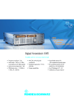
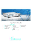
Agilent 8657A/8657B
Signal Generators
Profile
Spectral performance for general-purpose test
Overview
The Agilent Technologies 8657A and 8657B signal generators are designed to test AM, FM, and pulsed receivers
as well as components. With their exceptional analog
modulation, good spectral purity, and superb output
level performance, these signal generators are ideal for
R&D, manufacturing, and support.
In-channel performance
Measurement confidence
The 8657A and B signal generators provide the spectral
purity and modulation versatility needed for RF testing
of communication and navigation equipment.
Low residual FM ensures wide hum and noise test margins
Hum and noise testing requires a signal generator to
have low residual FM to ensure no measurement error.
The residual FM of the 8657A and B provides the test
margins you need for the most demanding hum and
noise tests.
Output level range and accuracy for sensitivity testing
With a dynamic range from +13 to –143.5 dBm, the
8657A and B allow sensitivity measurements to be made
on even the most sensitive receivers. The 8657A and B
couple this with a level accuracy of ±1 dB (typically
0.5 dB) to –127 dBm across the full temperature range of
0 to 55 degrees C, to give you accurate and repeatable
measurements every time.
Low RF leakage eliminates measurement interference
Sensitivity measurements can often be masked by RF
leakage (radiated emissions). With the 8657A and B, RF
leakage is reduced to a level that assures virtually no
measurement interference.
DCFM faithfully reproduces digital signals
For radios with digital squelching, the 8657A and B have
extremely stable dc-coupled FM (dcFM). The dc coupling
of low-rate tones or digital data eliminates droop, and
the exceptional stability and center-frequency accuracy
when in dcFM mode eliminates the need to retune the
signal generator after dcFM is selected.
Pulse modulation with the 8657B
High-performance pulse modulation (available on the
8657B) will give you confidence in your radar or pulsed
carrier measurements. This includes rise/fall times of
<35 ns, rates from dc to 30 MHz, and better than 70 dB
on/off ratios (fc<1030 MHz).
Out-of-channel measurements with the 8657A/B
Automated tests
Low single-sideband phase noise for adjacent channel selectivity
testing
A receiver’s ability to reject unwanted signals is measured using out-of-channel tests. With its good spectral
purity, the 8657A and B make it easy to perform
demanding tests such as adjacent channel selectivity
measurements.
Reliable output attenuators
With production lines requiring ever-faster throughput,
test equipment must be more reliable than ever. Output
level cycling requires electromechanical relays to switch
in and out of different attenuators to produce varying
output levels. The 8657A and B enhance system up-time
by using a very reliable attenuator technology. The
8657A is especially dependable with its electronic attenuator design. Instead of using mechanical relays for
switching the attenuators, the 8657A uses solid-state
components for setting output levels. The patented
design uses PIN-diode switching elements with 3 million
hours mean time between failure rate. This exceptional
reliability is backed with a 5-year warranty against
attenuator failure.
Adjacent channel selectivity measures a receiver’s ability
to pick out a desired signal while rejecting a strong signal one channel away. To measure adjacent channel
selectivity the out-of-channel signal generator must have
low single-sideband (SSB) phase noise and nonharmonic
spurious content at channel spacings, otherwise the inchannel signal is masked. The exceptional phase noise
performance of the 8657A and B provides a cost-effective
solution for many out-of-channel tests.
General purpose and component tests
Output power to drive high-level inputs
For applications requiring high output power, the 8657A
and B can overrange beyond the +13 dBm specified output level to >+16 dBm for most frequencies.
DCFM for VCO simulation
State-of-the-art dcFM and wide FM bandwidth make the
8657A and B ideal sources for many VCO simulation
applications. For example, the 8657A or B can be used to
replace a receiver’s VCO during design.
Phase adjust to characterize phase-sensitive devices
The 8657A and B give you the ability to adjust the phase
of the output signal in one-degree increments with
respect to a source that is locked to the same reference
timebase. This feature makes it easy to characterize
phase-detector or phase-interferometer receivers during
design or manufacturing.
Manual tests
100 nonvolatile store/recall registers save set-up time
The 8657A and B offer as a standard feature the ability
to store 100 complete instrument states. This feature
decreases set-up time when performing repetitive tests
and reduces operator errors.
Register sequencing provides semi-automation
Stepping through the store/recall registers is easy with
the front-panel sequence keys or the rear-panel remotesequence connector. These features allow the user to
sequence through the storage registers in any order.
2
Ordering information
Please contact your Agilent Technologies Sales and
Service Office for more information or visit our website
at www.agilent.com/find/tmdir
Option Description
001
002
003
1BN
1BP
907
908
909
910
915
W30
W32
W34
W50
W52
W54
High-stability timebase
Rear-panel connections
Pulse modulation ( 8657B only)
Mil std 45662A calibration certification
Mil std 45622A calibration with test data
Front handle kit
Rack flange kit
Rack flange kit w/ front handle
Adds operation/calibration manual and two service manuals
Adds service manual
3-year return repair service
3-year return calibration service
3-year standards compliant calibration service
5-year return repair service
5-year return calibration service
5-year standards compliant calibration service
Technical specifications
Output
Specifications describe the instruments warranted performance and apply after a 30-minute warm-up. All
specifications are valid over the signal generator’s entire
operating/environment range unless otherwise noted.
Range (dBm)
8657A
Supplemental characteristics (indicated by italic type) are
intended to provide information useful in estimating
instrument capability in your application by describing
typical, but not warranted, performance.
Note: The upper frequency range of the 8657A is 1.04 GHz.
Specifications above 1.04 GHz apply only to the 8657B.
8657B
Resolution
Absolute level accuracy3
8657A
8657B
Frequency
Range
8657A
8657B
Underrange
100 kHz to 1.04 GHz
100 kHz to 2.6 GHz
To 10 kHz with uncalibrated output and
modulation.
Resolution
8657A
8657B
Accuracy and stability
Switching speed1
Phase offset
10 Hz
1 Hz
Same as timebase
<35 ms.2 (30 ms typical at 25 °C)
Output signal phase is adjustable in
1-degree nominal increments.
Level flatness
100 kHz to 2.06 GHz
Reverse power protection
to maximum output frequency)
Maximum DC voltage
SWR
8657A (fc(400 kHz)
8657B
Output impedance
+13 dBm to –143.5 dBm into 50 Ω,
+10 dBm to –143.5 dBm for frequencies
from 100 kHz to 1 MHz
+13 dBm to –143.5 dBm into 50 Ω,
+10 dBm to –143.5 dBm with pulse
modulation installed at fc<1.03 GHz
0.1 dB
<±1.5 dB (>+7 dBm)
<±1.0 dB (+7 to –127 dBm)
<±1.5 dB (<–127 dBm)
<±1.5 dB (>+3.5 dBm)
<±1.0 dB (+3.5 to –127 dBm)
<±1.5 dB (<–127 dBm)
±0.5 dB, output level setting of 0 dBm
50 watts (from a 50 Ω source)
8657A, 50 V
8657B, 25 V
<1.5 for levels <–3.5 dBm
<2.0 for levels ≤ +13 dBm
<1.5 for levels ≤ –6.5 dBm
<2.0 for levels ≤ +13 dBm
50 Ω nominal
Internal reference oscillator
Aging rate
Std. (typ.)
±2 ppm/yr
Temperature
(0 to 55 °C)
±10 ppm
Line voltage
Frequency
50 MHz
Timebase reference
output (rear panel)
External reference input
(rear panel)
High-stability Option 001
8657A, 1.5 x 10⁻⁸ parts/day after 10 days
1.0 x 10⁻⁹ parts/day after 180 days
8657B, 1.0 x 10⁻⁹ parts/day after 45 days
1. To be within 100 Hz of carrier frequency.
2. Add 5 ms when switching to fc>1.03 GHz for the 8657B.
3. Absolute level accuracy includes allowances for detector linearity, temperature,
flatness, attenuator accuracy and measurement uncertainty.
7 x 10⁻⁹
2 x 10⁻⁹ (+5%, –10%)
10 MHz
Available at a level of >0.15 Vrms into
50 Ω (output of 10, 5, or 1 MHz is selectable via internal jumper). If external reference is used, output will be the same
frequency.
Accepts any 10, 5, or 1 MHz ±0.002%)
Frequency standard at a level
>0.15 Vrms into 50 Ω
3
Spectral purity
SSB phase noise (in CW mode, at 20 kHz offset)
0.1 to 130 MHz
<–124 dBc/Hz
(<–130 dBc/Hz, typical)
130 to 260 MHz
<–136 dBc/Hz
(<–140 dBc/Hz, typical)
260 to 520 MHz
<–130 dBc/Hz
(<–136 dBc/Hz, typical)
520 MHz to 1.04 GHz
<–124 dBc/Hz
(<–130 dBc/Hz, typical)
1.04 to 2.06 GHz
<–118 dBc/Hz
(<–123 dBc/Hz, typical)
Residual FM (CW mode, rms)
Frequency range
Post detection BW
(rms detector)
300 Hz to 3 kHz
0.1 to 130 MHz
130 to 260 MHz
260 to 520 MHz
520 MHz to1.04 GHz
<4 Hz (typical <2 Hz)
<1 Hz (typical <0.5 Hz)
<2 Hz (typical <1 Hz)
8657A, <4 Hz (typical <1 Hz)
8657B, <3 Hz (typical <1 Hz)
1.04 to 2.06 GHz
<6 Hz (typical <2 Hz)
50 Hz to 15 kHz1
<6 Hz (typical <3 Hz)
<1.5 Hz (typical <1 Hz)
<3 Hz (typical <1 Hz)
8657A, <6 Hz
8657B, <4 Hz (typical
<1.5 Hz)
<8 Hz (typical <3 Hz)
1. Typical residual FM specifications for the 50 Hz to 15 kHz post detection bandwidth apply only to the 8657B.
Typical Agilent 8657A SSB phase noise at 500 MHz
Typical Agilent 8657B SSB phase noise at 500 MHz
4
Residual AM (50 Hz to 15 kHz post-detection noise bandwidth, in CW
mode)
<0.04% AM
Frequency modulation
Harmonics (≤+7 dBm output levels)1
8657A
8657B
0.1 to 1.03 GHz
1.03 to 1.8 GHz
1.8 to 2.06 GHz
<–30 dBc
<–30 dBc
<–25 dBc
<–25 dBc
Center frequency
0.1 to 130 MHz
Subharmonics (≤+7 dBm output levels)
8657A, 8657B
0.1 to 1.03 GHz
8657B
1.03 to 1.8 GHz
1.8 to 2.06 GHz
None
<–40 dBc
<–35 dBc
Maximum FM peak deviation3
AC mode (the lesser of)
4000 x rate (Hz) or DC mode
max. deviation
130 to 260 MHz
1000 x rate (Hz) or DC mode
max. deviation
260 to 520 MHz
2000 x rate (Hz) or DC mode
max. deviation
520 MHz to 1.04 GHz 4000 x rate (Hz) or DC mode
max. deviation
1.04 to 2.06 GHz
8000 x rate (Hz) or DC mode
max. deviation
DC mode
8657A, 99 kHz
8657B, 200 kHz
8657A, 50 kHz
8657B, 50 kHz
8657A, 99 kHz
8657B, 100 kHz
8657A, 99 kHz
8657B, 200 kHz
8657B, 400 kHz
Nonharmonics (CW mode)
Frequency range
0.1 to 130 MHz
Offset from carrier
5 kHz to 2 MHz
8657A, <–60 dBc
8657B, <–63 dBc (typical)
130 to 260 MHz
8657A, <–72 dBc
8657B, <–75 dBc (typical)
260 to 520 MHz
8657A, <–66 dBc
8657B, <–66 dBc (typical)
520 MHz to 1.04 GHz2 8657A, <–60 dBc
8657B, <–63 dBc (typical)
1.03 to 2.06 GHz
8657B, <–57 dBc (typical)
>2 MHz
Resolution
8657A
<–60 dBc
8657B
<–60 dBc
<–60 dBc
<–60 dBc
<–54 dBc
100 Hz for deviations < 10 kHz;
1 kHz for deviations ≥ 10 kHz
100 Hz (200 Hz for carrier frequency >1.04 GHz)
for deviations <20 kHz;
200 Hz (400 Hz for carrier frequency >1.04 GHz)
for deviations >20 kHz
FM rate
Internal
400 Hz and 1 kHz, ±2%
External
(referenced to 1kHz) dc/5 Hz to 100 kHz, 3 dB bandwidth; dc/20 Hz to
50 kHz, 1 dB bandwidth
1. Spurious specifications apply for output levels ≤+4 dBm and fc<1.03 GHz when
pulse modulation is installed (8657B) only.
2. 520 MHz to 1.03 GHz for 8657B.
3. FM not specified when peak deviation is >(fc –100 kHz).
5
Center frequency accuracy in dc mode
Amplitude modulation
Carrier frequency
Center frequency accuracy
Range
8657A3
0.1 to 130 MHz
130 to 260 MHz
260 to 520 MHz
520 MHz to 1.04 GHz
1.04 to 2.06 GHz
±500 Hz
±125 Hz
±250 Hz
±500 Hz
±1000 Hz
Center frequency
stability in dc mode
<10 Hz per hour drift (typical <3 Hz per
hour)
Distortion (at internal rates)1
<0.5% THD plus noise (typical <1.5% for
all specified deviations and rates)
Sensitivity
1 Vpeak for indicated accuracy, 1 Vdc
when in dc-FM mode
8657B5
Resolution
Indicator accuracy (internal rates) <±5% of setting
Incidental AM (peak deviations
<20 kHz, internal rates)
fc>500 kHz
fc>1.03 GHz2
0 to 99%, level ≤+7 dBm, fc ≥400 kHz4
0 to 30%, level ≤+10 dBm, fc ≥400 kHz4
0 to 100%, level ≤+7 dBm, fc ≥400 kHz
0 to 30%, level ≤+10 dBm, fc ≥400 kHz
<0.1% AM
<0.5% AM
1%
Rates
Internal
External
400 Hz and 1 kHz, ±2%
20 Hz to 40 kHz (1dB bandwidth);
8657B, typical, 20 Hz to 100 kHz
(3 dB bandwidth)
Distortion (internal rates, level <+7 dBm)
AM depth
0 to 30% AM
31 to 70% AM
71 to 90% AM
fc<1.04 GHz
<1.5%
<3.0%
<4.0%
fc>1.04 GHz
4%
4%
7%
Sensitivity (typical) 1 Vpeak for indicated accuracy
Indicator accuracy (for depths <90%
and internal rates and levels ≤+7 dBm)
Incidental phase modulation
(at 30% AM depth, internal rates)
<±(2% + 6% of setting)
<0.3 radians peak
1. 8657A only. FM distortion only specified for deviations up to 25 kHz for
130<fc<260 MHz, and for 260<fc<520 MHz.
2. 8657B only.
3. AM depth is further limited by indicator accuracy specifications.
4. 8657A only. For fc<400 kHz, AM depths of 0 to 30%, levels ≤+7 dBm.
5. 8657B only. When pulse modulation is installed, maximum specified output level
in AM is reduced by 3 dB when fc<1.03 GHz.
6
External modulation input
Maximum repetition rate
dc to 30 MHz, typical
Front panel BNC, 600 Ω dc-coupled; front panel annunciators indicate 1 V
peak signal ±5%.
Level accuracy
±1.0 dB, typical
Duty cycle
0 to 100%, typical (limited by rise/fall
time)
Pulse modulation input
BNC, high impedance (internally selectable to 50 ohms), can be driven directly
by TTL
Maximum input level
±15 V, typical
Nominal input threshold
1.6 V, typical
Video feedthrough
<15%, typical
Modulating signal output
Internal modulating signal is provided at the front panel BNC connector at
nominally 1 V peak into a 600 Ω resistive load.
Simultaneous modulation
Internal/External
Internal/Internal
External/External
AM/FM, FM/AM, AM/AM, FM/FM,
AM/FM/(Pulse1)
AM/FM
AM/FM
Pulse time delay2
On to off
Off to on
34 ns, typical
47 ns, typical
Pulse modulation (Agilent 8657B only)1
Remote programming
On/off ratio
fc ≥130 MHz
fc ≥1.03 GHz
Rise/fall times
fc ≥130 MHz
fc ≥1.03 GHz
>70 dB
>95 dB
>35 ns
>50 ns
Interface
GPIB (IEEE-488)
IEEE-488 functions
SH0, AH1, T0, L2, SR0, RL1, PP0, DC1,
DT0, C0, E1
1. 8657B only. Pulse modulation specifications apply for carriers >130 MHz and levels ≤+7 dBm (frequency switching speed typically increases by 30 ms with pulse
modulation on). Additionally, AM is unspecified with pulse modulation turned on
at fc≥1.03 GHz.
2. Time delay between a change in input pulse and carrier response.
7
By internet, phone, or fax, get assistance with all your
test and measurement needs.
General
Operating temperature range
0 to 55 °C
Storage temperature range
–40 to +71 °C
Leakage
Conducted and radiated interference is
within the requirements of RE02 (and
CE03 for the 8657B, except broadband
conducted below 70 kHz) of MIL STD
461B, and FTZ 1046 (FTZ 1115 for
8657B). Furthermore, RF leakage of less
than 1.0 µV is induced in a two-turn
loop, 2.5 cm in diameter, held 2.5 cm
away from the front surface. (Typical
leakage for the 8657Bis <0.05 µV for
levels <–40 dBm.)
Online Assistance
www.agilent.com/find/assist
Phone or Fax
United States:
(tel) 1 800 452 4844
Canada:
(tel) 1 877 894 4414
(fax) (905) 206 4120
Europe:
(tel) (31 20) 547 2323
(fax) (31 20) 547 2390
Japan:
(tel) (81) 426 56 7832
(fax) (81) 426 56 7840
Save/recall/sequence
storage registers
100 non-volatile registers are available
to save front panel settings.
Latin America:
(tel) (305) 269 7500
(fax) (305) 269 7599
Rear-panel SEQ input level
TTL low to recall next storage register
contents.
Australia:
(tel) 1 800 629 485
(fax) (61 3) 9272 0749
Power requirements
100 or 120 or 220 or 240 volts (+5%,
–10% for 8657A; ±10% for 8657B) from
48 to 440 Hz; 160 VA maximum for
8657A (200 VA maximum for 8657B).
IEC 1010 compliant.
Weight
Dimensions
8657A, net 18.2 kg (40 lb);
shipping 23.6 kg (52 lb)
8657B, net 20.5 kg (45 lb);
shipping 26.0 kg (57 lb)
133 mm H x 425 mm W x 574 mm D
(5.25 in H x 16.75 in W x 22.6 in D)
New Zealand:
(tel) 0 800 738 378
(fax) (64 4) 495 8950
Asia Pacific:
(tel) (852) 3197 7777
(fax) (852) 2506 9284
Product specifications and descriptions in this
document subject to change without notice.
Copyright © 1998, 2000 Agilent Technologies
Printed in U.S.A. 8/00
5968-2704E