1
SERVICE MANUAL
MULTIPLE OUTPUT LINEAR SYSTEM
DC POWER SUPPLIES
Agilent MODELS 6621A, 6622A,
6623A, 6624A, and 6627A
Agilent Part No 5957-6379
Agilent Model 6621A, Serial 3737A-03086 through 03145
US37370101 and up
Agilent Model 6622A, Serial 3736A-04021 through 04040
US37360101 and up
Agilent Model 6623A, Serial 3736A-05451 through 05530
US37360101 and up
Agilent Model 6624A, Serial 3735A-13801 through 14200
US37350101 and up
Agilent Model 6627A, Serial 3735A-02356 through 02510
US37350101 and up
* For instruments with higher Serial Numbers, a change page may be included.
5
Microfiche Part No. 5957-6380
Printed in Malaysia: September, 2001
CERTIFICATION
Agilent Technologies certifies that this product met its published specifications at time of shipment from the factory. Agilent
Technologies further certifies that its calibration measurements are traceable to the United States National Bureau of
Standards, to the extent allowed by the Bureau’s calibration facility, and to the calibration facilities of other International
Standards Organization members.
WARRANTY
This Agilent Technologies hardware product is warranted against defects in material and workmanship for a period of three
years from date of delivery. Agilent software and firmware products, which are designated by Agilent for use with a
hardware product and when properly installed on that hardware product, are warranted not to fail to execute their
programming instructions due to defects in material and workmanship for a period of 90 days from date of delivery. During
the warranty period Agilent Technologies will, at its option, either repair or replace products which prove to be defective.
Agilent does not warrant that the operation for the software, firmware, or hardware shall be uninterrupted or error free.
For warranty service, with the exception of warranty options, this product must be returned to a service facility designated
by Agilent. Customer shall prepay shipping charges by (and shall pay all duty and taxes) for products returned to Agilent
for warranty service. Except for products returned to Customer from another country, Agilent shall pay for return of
products to Customer.
Warranty services outside the country of initial purchase are included in Agilent’s product price, only if Customer pays
Agilent international prices (defined as destination local currency price, or U.S. or Geneva Export price).
If Agilent is unable, within a reasonable time to repair or replace any product to condition as warranted, the Customer shall
be entitled to a refund of the purchase price upon return of the product to Agilent.
LIMITATION OF WARRANTY
The foregoing warranty shall not apply to defects resulting from improper or inadequate maintenance by the Customer,
Customer-supplied software or interfacing, unauthorized modification or misuse, operation outside of the environmental
specifications for the product, or improper site preparation and maintenance. NO OTHER WARRANTY IS EXPRESSED
OR IMPLIED. AGILENT SPECIFICALLY DISCLAIMS THE IMPLIED WARRANTIES OF MERCHANTABILITY
AND FITNESS FOR A PARTICULAR PURPOSE.
EXCLUSIVE REMEDIES
THE REMEDIES PROVIDED HEREIN ARE THE CUSTOMER’S SOLE AND EXCLUSIVE REMEDIES. AGILENT
SHALL NOT BE LIABLE FOR ANY DIRECT, INDIRECT, SPECIAL, INCIDENTAL, OR CONSEQUENTIAL
DAMAGES, WHETHER BASED ON CONTRACT, TORT, OR ANY OTHER LEGAL THEORY.
ASSISTANCE
The above statements apply only to the standard product warranty. Warranty options, extended support contracts, product
maintenance agreements and customer assistance agreements are also available. Contact your nearest Agilent
Technologies Sales and Service office for further information on Agilent’s full line of Support Programs.
SAFETY SUMMARY
The following general safety precautions must be observed during all phases of operation, service, and repair of this
instrument. Failure to comply with these precautions or with specific warnings elsewhere in this manual violates safety
standards of design, manufacture, and intended use of the instrument. Agilent Technologies assumes no liability for the
customer’s failure to comply with these requirements.
BEFORE APPLYING POWER.
Verify that the product is set to match the available line voltage and the correct fuse is installed.
GROUND THE INSTRUMENT.
This product is a Safety Class 1 instrument (provided with a protective earth terminal). To minimize shock hazard, the instrument chassis
and cabinet must be connected to an electrical ground. The instrument must be connected to the ac power supply mains through a threeconductor power cable, with the third wire firmly connected to an electrical ground (safety ground) at the power outlet. For instruments
designed to be hard-wired to the ac power lines (supply mains), connect the protective earth terminal to a protective conductor before any
other connection is made. Any interruption of the protective (grounding) conductor or disconnection of the protective earth terminal will
cause a potential shock hazard that could result in personal injury. If the instrument is to be energized via an external autotransformer for
voltage reduction, be certain that the autotransformer common terminal is connected to the neutral (earthed pole) of the ac power lines
(supply mains).
FUSES.
Only fuses with the required rated current, voltage, and specified type (normal blow, time delay, etc.) should be used. Do not use repaired
fuses or short circuited fuseholders. To do so could cause a shock or fire hazard.
DO NOT OPERATE IN AN EXPLOSIVE ATMOSPHERE.
Do not operate the instrument in the presence of flammable gases or fumes.
KEEP AWAY FROM LIVE CIRCUITS.
Operating personnel must not remove instrument covers. Component replacement and internal adjustments must be made by qualified
service personnel. Do not replace components with power cable connected. Under certain conditions, dangerous voltages may exist even
with the power cable removed. To avoid injuries, always disconnect power, discharge circuits and remove external voltage sources before
touching components.
DO NOT SERVICE OR ADJUST ALONE.
Do not attempt internal service or adjustment unless another person, capable of rendering first aid and resuscitation, is present.
DO NOT EXCEED INPUT RATINGS.
This instrument may be equipped with a line filter to reduce electromagnetic interference and must be connected to a properly grounded
receptacle to minimize electric shock hazard. Operation at line voltages or frequencies in excess of those stated on the data plate may
cause leakage currents in excess of 5.0 mA peak.
SAFETY SYMBOLS.
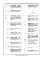
Instruction manual symbol: the product will be marked with this symbol when it is necessary for the user to refer to the
instruction manual (refer to Table of Contents) .
Indicates hazardous voltages.
Indicate earth (ground) terminal.
The WARNING sign denotes a hazard. It calls attention to a procedure, practice, or the like, which, if not correctly
performed or adhered to, could result in personal injury. Do not proceed beyond a WARNING sign until the
indicated conditions are fully understood and met.
The CAUTION sign denotes a hazard. It calls attention to an operating procedure, or the like, which, if not correctly
performed or adhered to, could result in damage to or destruction of part or all of the product. Do not proceed
beyond a CAUTION sign until the indicated conditions are fully understood and met.
DO NOT SUBSTITUTE PARTS OR MODIFY INSTRUMENT.
Because of the danger of introducing additional hazards, do not install substitute parts or perform any unauthorized modification to the
instrument. Return the instrument to an Agilent Technologies Sales and Service Office for service and repair to ensure that safety features
are maintained.
Instruments which appear damaged or defective should be made inoperative and secured against unintended operation until they can be
repaired by qualified service personnel
SAFETY SUMMARY (continued)
GENERAL
Any LEDs used in this product are Class 1 LEDs as per IEC 825-1.
ENVIRONMENTAL CONDITIONS
This instrument is intended for indoor use in an installation category II, pollution degree 2 environment. It is designed to
operate at a maximum relative humidity of 95% and at altitudes of up to 2000 meters. Refer to the specifications tables for the
ac mains voltage requirements and ambient operating temperature range.
SAFETY SYMBOL DEFINITIONS
Symbol
Description
Symbol
Description
Direct current
Terminal for Line conductor on permanently
installed equipment
Alternating current
Caution, risk of electric shock
Both direct and alternating current
Caution, hot surface
Three-phase alternating current
Caution (refer to accompanying documents)
Earth (ground) terminal
In position of a bi-stable push control
Protective earth (ground) terminal
Out position of a bi-stable push control
Frame or chassis terminal
On (supply)
Terminal for Neutral conductor on
permanently installed equipment
Off (supply)
Terminal is at earth potential
(Used for measurement and control
circuits designed to be operated with
one terminal at earth potential.)
Standby (supply)
Units with this symbol are not completely
disconnected from ac mains when this switch is
off. To completely disconnect the unit from ac
mains, either disconnect the power cord or have
a qualified electrician install an external switch.
Herstellerbescheinigung
Diese Information steht im Zusammenhang mit den Anforderungen der
Maschinenläminformationsverordnung vom 18 Januar 1991.
* Schalldruckpegel Lp <70 dB(A)
* Nach EN 27779 (Typprüfung).
* Am Arbeitsplatz
* Normaler Betrieb
Manufacturer’s Declaration
This statement is provided to comply with the requirements of the German Sound Emission Directive,
from 18 January 1991.
* Sound Pressure Lp <70 dB(A) * At Operator Position
* According to EN 27779 (Type Test).
Edition 2
September, 2001
© Copyright 2001 Agilent Technologies, Inc.
* Normal Operation
CONTENTS
Section I
INTRODUCTION
1-1
1-2
1-3
1-4
Section IV
TROUBLESHOOTING
SCOPE …............…..………………...............................1-1
SAFETY CONSIDERATIONS ….............................….1-1
INSTRUMENT AND MANUAL
IDENTIFICATION ..……………….…………….........1-1
FIRMWARE REVISIONS…...……...............................1-2
4-1
4-2
4-3
4-4
4-5
4-6
4-7
4-8
4-9
4-10
4-11
4-12
4-13
4-14
Section II
PRINCIPLES OF OPERATION
2-1
2-2
2-3
2-4
2-5
2-6
2-7
2-8
2-9
2-16
2-20
2-23
2-24
2-25
2-34
INTRODUCTION .………........................................... 2-1
OVERALL BLOCK DIAGRAM DESCRIPTION
(Figure 2-1) …..………………………………………..2-1
AC Input Circuits …………….....................................2-1
GPIB Board ……….......................................................2-1
Front Panel …………………………………………….2-1
Output Board ………………………………………….2-1
GPIB Board (Figure 2-3) …………………………….2-2
GPIB Interface ….……………………………………2-3
System MicroComputer ...……………………………2-4
Output Boards Interface.……..................................... 2-4
Front Panel Interface ……........................................…2-5
Bias Supply and Start Up ……....................................2-5
OUTPUT BOARD ......................................………..…2-7
Secondary Interface Circuits
(Figure 2-4) ……………………………………………2-7
Power Mesh and Control Circuits
(Figure 2-5)……………………………………......…. 2-10
4-15
4-16
4-17
4-18
4-19
4-20
4-21
4-22
4-23
4-24
4-25
4-26
4-27
4-28
4-29
Section III
VERIFICATION
3-1
3-2
3-3
3-4
3-5
3-6
3-10
3-21
3-29
3-30
3-35
3-36
3-37
3-38
INTRODUCTION …………......................................... 3-1
TEST EQUIPMENT REQUIRED …………………….3-1
OPERATION VERIFICATION TESTS……............... 3-1
PERFORMANCE TESTS...............................………....3-1
Introduction .................................................…………..3-1
Measurement Techniques ……………………………3-1
Constant Voltage (CV) Tests …….............................. 3-4
Constant Current (CC) Tests ......………....................3-10
EXTENDED TESTS……………..................................3-13
Output Drift Tests.....................................…………...3-13
TEMPERATURE COEFFICIENT (TC) TESTS ..…...3-14
Output Voltage and Readbauk Voltage TC ......…...3-14
Output Current and Readback Current TC ..……...3-15
Negative Current Limit (-CC) Readback TC .......…3-15
4-30
4-33
4-34
INTRODUCTION ……………………………………..4-1
ELECTROSTATIC PROTECTION ………………..…4-1
REMOVAL AND REPLACEMENT …………………4-2
Top Cover Removal …………………………………..4-2
Gaining Access to Assemblies in the Supply…….…4-2
GPIB Board Removal ………………………………4-2
40 Watt Output Board Removal……………………...4-2
80 Watt Output Board Removal……………………...4-4
Replacing the power Module U338 (U339) …………4-4
Front Panel Removal ………………………………….4-4
Chassis Mounted Components………………………4-5
TEST EQUIPMENT REQUIRED ..…………………4-5
FUSE REPLACEMENT …………………………….…4-5
INITIAL TROUBLESHOOTING AND
BOARD ISOLATION PROCEDURES ……………....4-8
Power-On Self Test ……………………………………4-8
Connector P201 Jumper Positions …………………..4-9
ERROR Codes and Messages ………………………...4-9
GPIB BOARD AND FRONT PANEL
TROUBLESHOOTING PROCEDURES……………4-13
Test Setup ……………………………………………..4-13
Post Repair Calibration ...……................................... 4-13
Setting the Model Number
(MODEL Command) ..……...................................... 4-13
Signature Analysis Testing……….............................4-14
Test Setup for S.A......................................………….. 4-14
Firmware Revisions (ROM? Command) ……..........4-14
OUTPUT BOARD TROUBLESHOOTING
PROCEDURES …………............................................ 4-30
Test Setup ………….................................................... 4-30
Post Repair Calibration ……….................................. 4-30
Self Exercise Routine on the Output Board……......4-30
Troubleshooting Analog Multiplexer U323 and
Readbadk Using VMUX? Command ....……….......4-49
Understanding and Troubleshooting the Signal
Processor (U327) …………..........................................4-50
Power Module Signal …………...............................4-54
Miscellaneous Trouble Symptoms
and Remedies ....................................……………......4-54
Section V
REPLACEABLE PARTS
5-1
5-2
i
INTRODUCTION ……………………………………..5-1
HOW TO ORDER PARTS ………………………….5-1
CONTENTS (Cont.)
Section VI
CIRCUIT DIAGRAMS
6-1
6-2
6-3
Appendix A
LOGIC SYMBOLOGY
INTRODUCTION ………....................…..................... 6-1
FUNCTIONAL SCHEMATIC DIAGRAMS ......……6-1
COMPONENT LOCATION………………………….6-1
ii
LIST OF FIGURES
Figure
2-1
2-2
2-3
2-4
2-5
2-6
2-7
2-8
2-9
3-1
3-2
3-3
3-4
3-5
3-6
3-7
3-8
3-9
3-10
3-11
3-12
4-1
4-2
4-3
4-4
4-5
4-6
4-7
4-8
4-9
4-10
4-11
4-12
4-13
4-14
4-15
4-16
4-17
4-18
4-19
4-20
6-1
6-2
6-2
6-3
6-3
6-4
6-4
6-5
6-5
Page
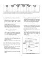
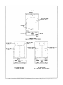
Agilent 6621A-6624 and 6627A Multiple Output Power Supplies, Block Diagram ………………………………………………2-2
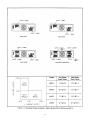
Output Operating Ranges for Agilent Models 6621A-6624A and 6627A ………………………………………………………….2-3
GPIB Board, Block Diagram ……………………………………………………….…………………………………………………2-6
Outpot Board, Secondary Interface Circuits, Block Diagram………………………………………………………………………..2-9
Outpot Board, Power Mesh and Control Circuits, Block …………………………………………………………………………..2-12
Voltage and Current Control Circuits, Simplified Schematic ……………………………………………………………………2-13
Typical Output Range Characteristics ……………………………………………………………………………………………….2-15
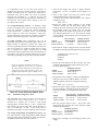
Typical Downprogramming Characteristics Below 2.0 V …………………………………………………………………………2-16
Overvoltage Protection Circuits, Block Diagram……………………………………………………………………………………2-18
Operating Ranges Available in Models 6621A-6624A and 6627A ………………………………………………………………….3-3
Current Monitoring Resistor Setup …………………………………………………………………………………………………….3-4
Basic Test Setup…………………………………………………………………………………………………………………………..3-5
Down Programming Speed Test Setup ………………………………………………………………………………………………..3-7
CV Down Programming Speed Test Waveforms …………………………………………………………………………………….3-7
CV UP Programming Speed Test Setup ……………………………………………………………………………………………….3-7
CV Up Programming Speed Test Waveforms………………………………………………………………………………………...3-8
Transient Recovery Time Test Setup …………………………………………………………………………………………………..3-9
Transient Response Waveform …………………………………………………………………………………………………………3-9
Fixed OV Protection Tea Setup…………………………………………………………………………………………………………3-9
OV External Trip Test Connections…………………………………………………………………………………………………...3-10
Negative Current Limit (-CC) Readback Accuracy …………………………………………………………………………………3-12
Agilent 6621A-6624A and 6627A Multiple Output Supplies, Assembly Locations ………………………………………………4-3
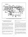
GPIB Board, Fuse and Test Point Locations ………………………………………………………………………………………….4-7
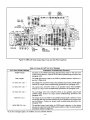
40WLV Output Board, Fuse and Test Point Locations …………………………………………………………………………….4-8
40WHV Output Board, Fuse end Test Point Locations……………………………………………………………………………..4-10
80WLV/80WHV Output Boards, Fuse and Test Point Locations ……………………………………………………………….4-11
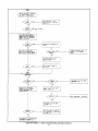
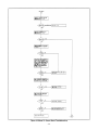
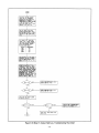
Initial Troubleshooting and Board Isolation…………………………………………………………………………………………4-15
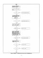
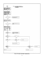
GPIB Board and Front Panel Troubleshooting ……………………………………………………………………………………..4-17
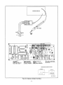
Signature Analysis Test Setup ………………………………………………………………………………………………………...4-19
Output Board Troubleshooting ……………………………………………………………………………………………………….4-31
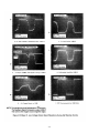
Low Voltage Output Board Waveforms During Self Exercise Routine…………………………………………………………...4-37
High Voltage Output Board Waveforms During Self Exercise Routine…………………………………………………………..4-39
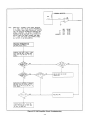
DAC Amplifier Circuit Troubleshooting …………………………………………………………………………………………….4-41
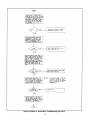
Overvoltage Troubleshooting …………………………………………………………………………………………………………4-42
Output Held Low Troubleshooting…………………………………………………………………………………………………...4-44
Output Held High Troubleshooting ………………………………………………………………………………………………….4-47
OV Circuit Will Not Trip Troubleshooting…………………………………………………………………………………………..4-48
Signal Processor U327, Overvoltage Circuit, Schematic Simplified……………………………………………………………….4-53
Signal Processor U327, Power-On/Start-Up Circuit, Schematic Simplified ……………………………………………………...4-53
Signal Processor U327, Status Monitor Circuit, Simplified Schematic ……………………………………………………………4-57
Status Problems Troubleshooting ………………………………….………………………………………………………………...4-58
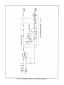
Power Distribution Schematic …………………………………………………………………………………………….……………6-5
GPIB Board, Component Location …...………………………………………………………………………………………………...6-7
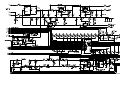
GPIB Board, Schematic Diagram …………………………………………………………………………………………………….....6-8
Output 1 & 2 Board, Component Location ………………………………….………………………………………………………...6-9
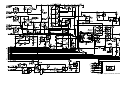
Output 1 & 2 Board, Schematic Diagram …………………………………….……………………………………………………..6-10
Output 3 & 4 Board, Component Location ………………………………….……………………………………………………….6-15
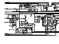
Output 3 & 4 Board, Schematic Diagram …………………………………….…………………………………………………….6-16
Output 1 & 2 80W Board, Component Location …………………………….………………………………………………………6-25
Output 1 & 2 80W Board, Schematic Diagram ……………………………….……………………………………………………...6-26
iii
LIST OF TABLES
Table
3-1
3-2
3-3
3-4
3-5
4-1
4-2
4-3
4-4
4-5
4-6
4-7
4-8
4-9
4-10
4-11
4-12
4-13
4-14
4-15
4-16
4-17
4-18
5-1
5-2
5-3
5-4
5-5
5-6
5-7
Page
Test Equipment Required for Verification ……………………………………………………………………………………………3-2
Low Range Voltage and Current Values ……………………………………………………………………………………………3-5
High Range Voltage and Current Values ……………………………………………………………………………………………3-6
Performance Test Record for 40WLV/80WLV Outputs ……………………………………………………………………………3-16
Performance Test Record for 40WHV/80WHV Outputs …………………………………………………………………………3-17
Test Equipment Required for Troubleshooting
…………………………………………………………………………………4-5
Fuses ………………………………………………………………………………………………………….…………………………...4-6
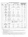
Tests Performed at Power-On …………………………………………………………………………………………………………..4-9
Power-On Self Test Error Messages …………………………………………………………………………………………………4-10
ERROR Codes and Messages ………………………………………………………………………………………………………….4-11
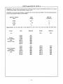
GPIB Board S.A. Test No. 1 …………………………………………………………………………………………………………...4-20
GPIB Board S.A. Test No. 2 …………………………………………………………………………………………………………...4-21
GPIB Board S.A. Test No. 3 …………………………………………………………………………………………………………...4-22
GPIB Board S.A. Test No. 4 …………………………………………………………………………………………………………...4-23
GPIB Board S.A. Test No. 5 …………………………………………………………………………………………………………...4-24
GPIB Board S.A. Test No. 6 …………………………………………………………………………………………………………...4-25
GPIB Board S.A. Test No. 7 …………………………………………………………………………………………………………...4-26
GPIB Board S.A. Test No. 8 …………………………………………………………………………………………………………...4-27
Keyboard Signal Paths …………………………………………………………………………………………………………………4-29
Microcomputer (U312) Signal Measurements During the Self Exercise Routine …………………………………………….4-49
Signal Processor (U327) Signal Levels ………………………………………………………………………………………………..4-51
Typical Power Module Voltage Levels……………………………………………………………………………………………….4-54
Miscellaneous Trouble Symptoms ……………………………………………………………………………………………………4-55
Output Board Configurations ………………………………………………………………………………………………………...5-1
Reference Designators…………………………………………………………………………………………………………………...5-1
Abbreviations …………………………………………………………………………………………………………………………….5-2
Federal Manufacturer Codes……………………………………………………………………………………………………………5-3
Model 6621-6624A and 6627A Multiple Output Power Parts List ………………………………………………………………….5-4
GPIB Board Parts List …………………………………………………………………………………………………………………5-8
Output Board Parts List………………………………………………………………………………………………………………...5-10
iv
Section I
INTRODUCTION
1-1
SCOPE
Replaceable Parts: Section V provides a listing of
replaceable parts for all electronic components and
mechanical assemblies.
This manual contains principles of operation, verification,
and troubleshooting information for the power supply.
Replaceable parts lists and circuit diagrams are also
provided. Installation, operation, programming, and
calibration procedures as well as detailed specifications are
given in a separate Operating Manual, Agilent Part No.
5957-6377.
Circuit Diagrams: Section VI contains functional schematics
and component location diagrams. The names that appear
on the functional schematics also appear on the block
diagrams in Section II. Thus, the descriptions in Section II
can be correlated with both the block diagrams and the
schematics.
Wherever applicable, the service instructions given in this
manual refer to pertinent information provided in the
Operating Manual. The information in each manual covers
all five models, 6621A-6624A and 6627A. The main
differences between the models are the number and type of
outputs each model contains. These differences are specified
in each of the manuals.
Logic Symbology: Appendix A gives a brief description of
the logic symbols used on the functional schematics.
Fault Indicator (FLT) and Remote inhibit (INH): A fault
indicator and remote inhibit circuit, which provide
additional shutdown protection should either the GPIB
and/or controller fail, are available optionally. See a
separate document entitled, "Appendix E Option 750
Operating Instructions" for the Multiple Output Linear
System DC Power Supply Agilent Models 6621A-6624A and
6627A (Agilent P/N 5957-6372).
The following is a listing of the information contained in
this manual with a brief description concerning its scope
and purpose.
Principles of Operation: Section II provides block diagram
level descriptions of the supply's circuits. The GPIB
interface (digital circuits), the power control (analog and
digital circuits), and power output (analog circuits) are
described. These descriptions are intended as an aid in
troubleshooting.
Computer Interface Intermediate Language (CIIL): Control
Interface Intermediate Language (CIIL) programming
capabilities (Option 700) are also available as an option. A
separate document entitled, Supplies Option 700" (Agilent
P/N 5957-6371)" describes the CIIL option.
Verification: Section III contains test procedures that check
the operation of the supply to ensure that it meets the
specifications given in Section I of the Operating manual.
1-2
SAFETY CONSIDERATIONS
This product is a Safety Class 1 instrument, which means
that it is provided with a protective earth terminal. The
instrument and this manual should be reviewed for safety
markings and instructions before operation. Refer to the
Safety Summary page at the beginning of this manual for a
summary of general safety information. Safety information
for specific procedures is located at appropriate places in the
manual.
Troubleshooting: Section IV contains board level
troubleshooting procedures to isolate a malfunction to a
defective board (GPIB or output board) or assembly (front
panel, power transformer, or cable assembly). Additional
troubleshooting procedures are provided to isolate the fault
to a defective component on the board. Board and assembly
level removal and replacement procedures are also given in
this section.
1-3
NOTE
INSTRUMENT AND MANUAL
IDENTIFICATION
Agilent Technologies instruments are identified by a twopart serial number, i.e. 2601A-00101. The first part of the
serial number (the prefix) is a number/letter combination
that denotes either the date of manufacture or the date of a
significant design change. It also indicates the country of
manufacture. The first two digits indicate the year (25
=1985, 26 =1986, etc), the second two digits indicate the
Calibration is generally required after a repair is made.
Software calibration procedures are given in Appendix A
of the Operating Manual. After calibration is completed,
perform the applicable test(s) given in Section III of this
manual to ensure that the supply meets all specifications.
1-1
described in this manual. The yellow change sheet may also
contain information for correcting errors in the manual.
week, and the "A" designates the U.S.A. The second part of
the serial number is a different sequential number assigned
to each instrument.
1-4 FIRMWARE REVISIONS
If the serial number prefix on your power supply differs
from that shown on the title page of this manual, a yellow
Manual Change sheet, supplied with the manual, defines
the differences between your supply and the supply
The Read Only Memory (ROM) chip inside of your supply
is identified with a label that specifies the revision of the
supply's firmware, see paragraph 4-24.
1-2
Section II
PRINCIPLES OF OPERATION
2-1
INTRODUCTION
user and the multiple outputs of the power supply. Each
output board is actually an output channel that can be
individually selected and controlled over the GPIB or from
the supply's front panel. The GPIB board interprets
commands from the GPIB or from the front panel to control
the selected output. The GPIB board also processes
measurement and status data received from the output
boards. This data may be read back to the controller over
the GPIB and/or displayed on the supply's front panel.
Also, each output board can be individually calibrated over
the GPIB using calibration commands (See Appendix A in
Operating Manual). Correction factors are calculated during
calibration and are stored in non-volatile memory on the
GPIB board. The GPIB board is described in greater detail in
paragraph 2-7.
The following paragraphs provide block diagram level
descriptions of the power supply. Differences between the
models are given as required. The descriptions provide a
basic understanding of circuit operation and are intended as
an aid in troubleshooting. It is assumed in the following
discussions that you are familiar with the operating and
programming instructions presented in the Operating
Manual (Agilent Part No. 5957-6377).
2-2
OVERALL BLOCK DIAGRAM
DESCRIPTION (FIGURE 2-1)
Figure 2-1 is a block diagram that illustrates the major
assemblies contained within the power supply. As shown in
the figure, each supply includes ac input circuits, an GPIB
board, front panel display and keyboard, and two or more
output boards.
2-3
2-5
Most of the remote operations that can be performed via the
GPIB can also be performed from the supply's front panel.
In addition to the ON/OFF switch already mentioned, the
front panel contains an LCD display and a keypad. The LCD
display consists of an alphanumeric display and status
annunciators. The LCD normally displays the measured
output voltage and current of the selected output. When
programming an output from the front panel keypad, the
selected output channel, the function being programmed,
and the present value will be displayed. The annunciators
indicate which output channel has been selected and give
GPIB power supply status information. The keypad allows
control of the supply's system functions as well as
individual control of each output channel. Detailed
instructions on using the front panel's display and keypad
are given in the Operating Manual.
AC Input Circuit
The ac input circuit consists of a line module on the rear
panel of the supply, front panel ON/OFF switch S1, power
transformer (T1), located in the front of the chassis, and a
cooling fan located in the rear of the chassis. The line
module contains a voltage selector card that selects the
applicable ac input voltage: 100 Vac, 120 Vac, 220 Vac, or
240 Vac. The voltage card selection must match the nominal
line voltage that is connected to the unit. The line module
also contains the main fuse F1. An 8 A fuse (normal blow)
must be installed for a 100/120 VAC input; a 4 A fuse
(normal blow) must be installed for a 220/240 Vac input.
The ac input is applied to the power transformer when S1 is
ON. Depending on the line module setting, the 120 VAC
cooling fan either runs directly from the line or from the
appropriate transformer tap. The power transformer
provides the main ac inputs to the output boards and also
provides the ac inputs for the bias voltage supplies located
on the GPIB board and each output board. Ac power
distribution is shown in detail in figure 6-1 in the rear of this
manual.
2-4
Front Panel
2-6
Output Boards
Each power supply model contains two or more (up to four)
output boards. The output combinations that correspond to
each model are shown in Figure 2-1. Each isolated output
can supply power in two ranges as shown in Figure 2-2.
This flexibility allows you to use the same output to power
loads with different voltage and current requirements. The
output ranges and operating characteristics of each output
are described in greater detail in Section IV of the Operating
Manual.
GPIB Board
As shown in Figure 2-1, each output board contains a
rectifier/filter, power module, control circuit, secondary
interface circuit, and bias supplies. Note that each 80 W
output board has two power modules connected in parallel.
The GPIB board contains the GPIB interface, system
microcomputer, output boards interface, and front panel
interface. These circuits provide the interface between the
2-1
2-2
The ac input to each output board is rectified, filtered, and
applied to the power module regulator. Each output board
employs series regulation techniques. The regulator element
is connected in series with the load and operates in the
linear region (between saturation and cutoff) of the
transistor characteristic curve. Regulation is achieved by
varying the conduction of the series element in response to
changes in the line voltage or the load. The constant voltage
CV control circuit compares the voltage at the output with a
reference voltage and generates a control signal which
varies the conduction of the series regulator to raise or
lower the output voltage as required. The constant current
CC control circuit compares the voltage at the current
monitor resistor with a reference and likewise varies the
conduction of the series regulator.
The functional names on the block diagram correspond with
those on the schematic so that the diagrams can be
correlated. As shown in Figure 2-3, the major circuits consist
of the GPIB interface, the system micro-computer, the
output boards interface, and the front panel interface circuit.
2-8
These circuits consist of the GPIB bus connector (J201),
transceivers (U203) for the 8 data lines and 8 control lines,
and the GPIB talker/listener chip (U202). All GPIB (IEEE488) functions are implemented by the GPIB chip which
handles data transfer between the microprocessor and the
GPIB, handshake protocol, and talker/listener addressing
procedures. The GPIB talker/listener chip is connected to
the data bus and appears as memory locations to the
microprocessor.
The interface circuit on the output board receives digital
signals from the GPIB board and converts them to analog
signals (reference voltages) which are sent to the control
circuit to program the output voltage and current.
The eight data lines (DI01-DI08) of the GPIB are reserved for
for the transfer of data and other messages in a byte serial,
bit parallel manner. Data and message transfer is
asynchronous, coordinated by the three handshake lines
(DAV, NRFD, and NDAC). The power supply can be a
talker or a listener on the GPIB. The controller dictates the
role of an GPIB device by setting the ATN (attention) line
true and sending talk or listen addresses on the data lines
(DI01-DI08). The power supply's GPIB address is stored in
the EEPROM (electrically erasable programmable memory)
chip along with other system variables. You can find out
your supply's GPIB address by using the front panel ADDR
key as described in the operating manual. As shipped from
the factory, the power supply's address is set to 5. Any
address from 0 through 30 is a valid address.
The output boards can be commanded to send
measurement and status data back to the GPIB controller
and/or to the display on the front panel. The data is sent
back via the secondary interface circuit and the appropriate
circuits on the GPIB board.
The output board is able to sink current as well as source
current. Current sink limits are fixed at values
approximately ten percent higher than the maximum
current source limit for the particular output voltage
operating point. See Figure 2-7 for typical current source
and sink characteristics. The output board circuits are
described in greater detail in paragraph 2-24.
2-7
GPIB Interface
There are five GPIB control lines: ATN, IFC, REN, SRQ, and
EOI (IEEE-488). When the controller sets the ATN line true,
all devices on the bus must "listen" to the addresses and
universal commands placed on the bus. When ATN is false,
only devices that are addressed will actively send or receive
data. All unaddressed devices will ignore the data lines
when ATN is false.
GPIB BOARD (FIGURE 2-3)
Figure 2-3 illustrates the major circuits and signal flow on
the GPIB board. Complete circuit details are shown on the
functional schematic, Figure 6-2, in the rear of this manual.
2-3
2-9
System Micro-Computer
looks like a 16-bit counter that continuously rolls over and
starts at zero. The contents of each address appear
sequentially on the data bus (other side of the break).In
addition, for all signature analysis tests, jumper W201 must
be moved from the NORM RUN position to the SIG
ANALYSIS position (see paragraph 4-23).
The system micro-computer decodes and executes all
instructions, and controls all data transfers. It consists of a
microprocessor, an address decoder, RAM and ROM
memories, data buffers/latches, and a real time clock as
shown in Figure 2-3.
2-13 Address Bus and Address Decoder. The
microprocessor has 16 address lines (A0-A15) allowing it to
address 65,536 locations. The address decoder (U208) allows
each addressable circuit
to look at a shorter address. The
____ ____
chip select signals ( CSO - CS8 )are decoded from the higher
order address lines (A12-A15). When a data buffer's CS is
decoded, it places its data on the data bus lines. When a data
latch's CS is decoded, the output of each latch will be set to
the logic state that is present on the associated data bus line.
If the chip select for the RAM (random access memory),
ROM (read only memory), or talker/listener chip is
decoded, the selected circuit will decode the lower order
address bits supplied to it on the address bus.
2-10 Microprocessor and Clock Circuits. These circuits
contain a high performance 8-bit microprocessor (U201) and
associated clock circuits. The microprocessor operates on a 1
MHz cycle, which it derives from__a 4 MHz ceramic
resonator oscillator(Y201).The 1 MHz Q signal is generated
by the microprocessor for use by the other circuits.
A 4 millisecond (approximately) clock signal, applied to the
microprocessor interrupt input, enables the microprocessor
to keep track of real time. This allows the microprocessor to
perform necessary tasks on a regular basis. The real time
clock signal is also used to keep track of the time that has
elapsed since the output was last changed. This enables the
microprocessor to determine if a CV/CC mode change
occurred
before
the
selected
time
delay
(see
Reprogramming Delay discussion in Section V of the
Operating Manual). The microprocessor inhibits the OCP
function until the delay is over.
2-14 Memory(ROM and RAM). The system microcomputer
contains both ROM (U206) and RAM (U207) devices. The 16
K non-volatile ROM contains the operating program and
parameters. The 2 K static RAM stores variables voltage to
be programmed, output current readback, etc. A third
memory chip, shown in the output boards interface block of
Figure 2-3,is the EEPROM (electrically erasable programmable memory). The EEPROM (U221) stores all of the
system constants including calibration constants, the
supply's GPIB address, and model number (see paragraph
2-19).
The microprocessor also uses the 4 millisecond clock to
determine when to refresh the front panel display and to
perform other regularly scheduled jobs.
__
The R/ W (read/write) output from the microprocessor
indicates the direction of flow on the data
__bus, either to or
from the microprocessor. A low level R/ W signal indicates
that the microprocessor
is writing data onto the data bus. A
__
high level R/ W signal indicates that the microprocessor is
reading data that was placed on the bus by the addressed
circuit. The microprocessor uses the address decoder circuit
and the address bus to specify the data transfer locations.
Addresses are valid on the rising edge of the Q signal.
2-15 Real Time Clock. The real time clock (U209) consists
of a 14-stage ripple counter that divides the 1 MHz Q clock
signal from the microprocessor to produce a pulse every 4
milliseconds. The real-time clock is used by the
microprocessor ______________
to schedule regular jobs as described
previously. The TIMER ENABLE signal resets the counter to
zero.
2-11 Data Bus Latches (U217) and Buffers (U216). The
timing sequence of the microprocessor is such that the
circuits providing data for the microprocessor are deselected (address disappears) before the microprocessor can
read the data. The data bus latches (U217) latch the data to
be read by the microprocessor. The data is updated on every
falling Q pulse. Data put on the data bus by the
microprocessor goes around the latches through buffers
(U216).
2-16 Output Boards Interface This circuit provides the
interface between the system microcomputer and each of
the output boards (up to 4) in the power supply. Data is
transferred serially one bit at a time between latches/buffers
on the GPIB board and opto-isolators on the output boards.
As shown in Figure 2-3, the latches/buffers use data bus
lines D0-D3 to send/receive data from the applicable
output. Data Line D0 is used for output board 1, D1 for
output board 2, D2 for output board 3 (if present), and D3
for output board 4 (if present). A controlled and regulated 5
volt line is also generated on the GPIB board to operate
part of the opto-isolators on the output boards. In addition
to interfacing with the output boards, the latches/buffers
interface with the 1 K bit serial EEPRO in which system
constants are stored.
2-12 Free-Run and Signature Analysis Jumpers. The data
bus is connected to the microprocessor through a jumper
pack (W202). For some signature analysis tests of the
microprocessor kernel (microprocessor, RAM, ROM), the
data bus is broken by moving W202 from the NORMAL
position to the NOP position (see paragraph 4-23). This
connects a NOP (no operation) code (free run) to the
microprocessor data inputs. The NOP code does not contain
an address for the next instruction so the microprocessor
goes to the next highest address. Therefore, the address bus
2-17 Data Buffers. These 3-state buffers (U212) place the
serial data from each output board and the EEPROM on the
supply’s
system microcomputer data bus lines when chip
____
select CS3 is decoded. Serial data from output boards 1-4
2-4
selected output board, the present function being
programmed, a programmed message, or an error message.
The annunciators provide operating and status information.
The microprocessor uses the real time clock to determine
when to update/refresh the display.
appears on data bus lines D0-D3, respectively, and
EEPROM serial output data appears on data bus line D7.
Logic 0's will always appear on data bus lines D4-D6 when
____
CS3 is decoded because these buffer inputs are connected to
COMMON. All buffer
____outputs are held in the high
impedance state when CS3 is not decoded.
Data bus lines D0-D2 are fed to the 3 to 8 line keyboard
decoder (U211). The microprocessor successively drives
each of the eight open collector outputs of the decoder and
monitors the four readback lines from the keyboard to
determine which key was pressed. The readback lines are
held high until a depressed key pulls the line low.
2-18 Data Latches. These stages (U213) are____
edge-triggered
D-type flip-flops. On the rising edge of the CS2 chip select,
the output of each stage will be set to the logic state that is
present on the associated data bus line. Data bus lines D0D3 are the serial data input lines for output
boards 1-4,
______________
respectively. Data bus line D4 controls the TIMER ENABLE
signal line to the real time clock circuit; D5 is the chip select
line for the EEPROM; D6 is the clock signal for the
EEPROM; and D7 is the data input line for the EEPROM.
2-22 Data Buffers. These 3-state buffers place the keyboard
____
readback data on data bus lines D4-D7 when chip select CS4
is decoded. As stated above, the microprocessor will use this
information to determine which key was pressed. In
addition to the keyboard readback data on D4-D7, the front
panel data buffers
____ provide the following data on bus lines
D0-D3 when CS4 is decoded:
D0 - A logic 1 (Jumper W201 is not installed in the
Skip Self Test position)--tells the microprocessor
to perform the self test at power on;
or
a logic 0 (Jumper W201 is installed in the Skip
Self Test position) - tells the microprocessor not
to perform self test at power on.
D1 - A logic 1 (jumper W201 is not installed in the Cal
Lockout position) - tells the microprocessor to
respond to calibration commands;
or
a logic 0 (Jumper W201 is installed in the Cal
Lockout position) - tells the microprocessor to
ignore calibration commands. This jumper
provides
security
against
unauthorized
calibration.
D2 - A logic 1 (this buffer input is hardwired).
D3 - A logic 0 (this buffer input is hardwired).
The data that is transferred between the GPIB board and
the output boards (up to 4) passes through optical isolators
located on each output board.
2-19 EEPROM. This 1 K bit serial EEPROM (electrically
erasable programmable memory) stores the power supply's
GPIB address and model number as well as the constants
used in calibrating the supply. The EEPROM (U221) is nonvolatile allowing it to retain the stored information after
power is cycled off and on.
Because the RAM operates faster than the EEPROM, at
power on, the stored serial data is read into RAM in the
system microcomputer via data bus line D7, the associated
buffer state, and the data output pin of the EEPROM.
The EEPROM's 1024 bits of read/write memory are divided
into 64 registers of 16 bits each. Each register can be serially
read from or written to using data bus line D7. Input data is
received via a data latch and output data is sent via a data
buffer.
All buffer outputs are held in the high
impedance state
____
disconnecting it from the data bus when CS4 is not decoded.
Data written to the EEPROM is stored in a location until it is
updated by an erase and write cycle. The CHIP SELECT and
CLOCK signals are used by the microprocessor to control
the EEPROM’s programming modes. At power on, the
EEPON signal holds the EEPROM's CLOCK signal off to
protect against accidental data writes when power is
initially applied.
2-20
2-23 Bias Supply and Start-Up Circuit
The bias supply (U218) provides + 5 V bias power to operate
the circuits on the GPIB board. The start-up circuit
(U220,U222) generates the OPTO PON signal (delayed + 5
V) which is used to power the optical-isolators on the
output boards. The OPTO PON signal is initially held low
for approximately 100 ms to prevent the erroneous transfer
of data at power on. The start-up circuit also generates
______
PCLR (power clear) and EEPON (EEPROM power on)
signals when power is turned on. The PCLR signal is held
low at power on to initialize the talker/listener and
microprocessor chips. The EEPON signal is held low at
power on to disable the EEPROM clock. Thus, the start up
circuit delays turning on the microprocessor and
optoisolators until the bias voltages have stabilized. If the
line voltage drops after the unit has been turned on, the
start-up circuit will again generate the low level signals to
disable the interface and remove power from the supply's
outputs.
Front Panel Interface
These circuits provide the interface between the supply's
system microcomputer and the front panel (keyboard and
LCD display). The microprocessor uses the data latches
(U210) and data buffers (U214) to transfer data between the
supply's system microcomputer and the front panel.
____
2-21 Data Latches. On the rising edge of the CS5 chip select
these D-type flip-flops will be set to the logic states that are
present on the data bus lines.
Data bus lines D2-D7 are fed directly to the front panel
display to indicate power supply conditions. The LCD
display may indicate the output voltage and current for a
2-5
2-6
2-24 OUTPUT BOARD
2-28 CV DAC. The constant voltage (CV) 12-bit DAC
(U313) and amplifier (U315A) convert the digital input into
an analog signal (CV REF) in the range of 0 to -10 V. This
signal is used as a reference voltage and is sent to the
voltage control circuits (see paragraph 2-43) to set the
output voltage to the programmed value. CV REF is also
sent to the analog multiplexer so that it can be measured
during power on self test.
The following paragraphs provide block diagram level
descriptions of the output board. The descriptions cover the
four output board types (40WLV, 40WHV, 8OWLV, and
80WHV). Differences between the board types are given as
required. Figure 2-1 shows which output board types are
used in each model.
The 12-bit DAC internally formulates the 12-bit DAC data
from the 8-bit (D0-D7) data bus. Bits D4-D7 are transferred
into DAC
__ bit positions 0-3 when the microcomputer sets the
DAC A/B signal low and bits D0-D7 are transferred into
DAC __
bit positions 4-11 when the microcomputer sets the
DAC A/B signal high.
The descriptions that follow are divided into two main
block diagram discussions: Secondary Interface Circuits and
Power Mesh and Control Circuits. The block diagrams
illustrate the major circuits and signal flow on an output
board. Complete circuit details are shown on the output
board functional schematic Figure 6-3 in the rear of the
manual. The functional names on the block diagrams
correspond with those on the functional schematic.
These circuits receive digital signals from the GPIB board
and convert them to analog signals (voltages) which are sent
to the power mesh and control circuits to program the
output voltage, output current, and overvoltage.
2-29 Current and Overvoltage DACs. These DACs__are
contained in a dual 8-bit DAC chip (U314). The DAC A/B
signal determines which DAC receives the data on the data
bus. Bits
__ D0-D7 are transferred into the current DAC when
DAC
__ A/B is low and into the overvoltage DAC when DAC
A /B is high.
Measurement and status signals are sent back to the
secondary interface circuits from the power mesh and
control circuits to be processed before they are sent on to the
GPIB board and then to the GPIB controller and/or the front
panel. The following paragraphs describe the interface
circuits shown in Figure 2-4.
The 8-bit current DAC (part of U314) and amplifier U315B
convert the digital input into an analog signal (CL REF) in
the range of 0 to -10 V. This signal is used as a reference
voltage and is sent to the current control circuit (see
paragraph 2-44) to set the output current to the
programmed value.
2-26 Microcomputer. This 8-bit microcomputer (U312)
contains a CPU, ROM, and RAM. These internal circuits
process all data that is transferred between the GPIB board
and the power mesh and control circuits on the output
board. GPIB board data is transferred serially via optical
isolators which connect incoming data to an input port on
the microcomputer and outgoing data to an output port on
the microcomputer.
The 8-bit overvoltage DAC (part of U314) and amplifier
U315C convert the digital input into an analog signal (OV
REF) in the range of 0 to -10 V. This signal is compared with
the output voltage and will shut down the output when the
output voltage exceeds the programmed OV (see paragraph
2-32).
2-25 Secondary Interface Circuits (Figure 2-4)
The CL REF and OV REF signals are also sent to the analog
multiplexer so that they can be measured during power on
self test.
On the output board side, the microcomputer uses an 8-bit
parallel bidirectional data bus to program DACs which
control the output voltage, output current, and overvoltage
setting. Various status and operating conditions are read
back on the data bus. The microcomputer also generates
address and control signals which are used by other
interface circuits. The interrupt input to the microcomputer
is used in conjunction with analog multiplexer (U323) and
DAC (U321) to perform a succesive approximation A/D
conversion in order to readback output voltage and current
values as well as various test point voltages.
2-30 Analog Multiplexer. The analog multiplexer
(U323)selects one of eight inputs (0 to -10 V) to be applied to
the readback signal comparator for the A/D converter. The
selected signal is determined by address lines (A0-A2)
which are received from the microcomputer. The analog
inputs to the multiplexer indicate the following:
COM
FUSE
2-27 Address Decoder. This circuit (U320) decodes
addresses sent by the microcomputer
and generates the
___ ___
appropriate chip select signal___
(CS0 - CS3) to select which
circuit sends or receives data. CS0 selects the status monitor
(part of U327) to send status data
back to the
________
microcomputer on data bus lines ___
D0-D5. CS1-CS3 determine
which DAC will receive data. CS1 selects the CV 12-bit
___
DAC, CS2 selects the + CC/OV dual 8-bit DAC, and CS3
selects the readback 12-bit DAC.
V READBACK
-I READBACK
+I READBACK
CV REF
CL REF
OV REF
2-7
- hardwired to common to reduce noise
when no signals are being sampled.
- output board's return fuse status
(read back during power-on self test)
- output voltage
- output current (sink)
- output current (source)
- voltage DAC output
- current DAC output
- overvoltage DAC output
flops were reset. The STATUS RESET input line from the
microcomputer resets the flip-flops.
The voltage readback buffer (U319C) provides unity gain for
the V READBACK signal and isolates the multiplexes circuit
from the CV control circuit (see Figure 2-5). The current
readback amplifier (U345) provides a gain of approximately
36 for the I-MON signal (0 to 0.25 V approximately) which
comes from the current sense resistor (see Figure 2-5). The
amplified signal is an input (+ IMON) to the analog
multiplexes and to the current readback inverter (P/O
U319D). The inverter slightly attenuates the signal and
provides the correct polarity to the analog multiplexes so
that the current can be monitored (- IMON) when the
output is sinking current (- current).
_________
The status monitor circuit
also receives OV SENSE and
_______
_______
THERM inputs. The THERM signal is received from the
power module(s) in the power mesh (see Figure 2-5) and
indicates when an overtemperature condition exists. Note
that when the microcomputer senses the overtemperature
(OT) condition via data bus line D4, it shuts down the
output. This circuit resets automatically and restores the
output approximately 30 seconds after the temperature
drops sufficiently for safe operation.
_________
The OV SENSE input signal indicates when the output's
overvoltage detector circuit has been tripped and the output
has been shut-down
overvoltage detector description
_______ (see _________
below). The THERM and OV SENSE inputs control the OT
and OV outputs of the status monitor. Note that the OT and
OV status____
are not____
held in____
flip-flops. All of status
monitor's
_______
outputs (CVO, + CLO, - CLO , OV, OT, and UNREG) are
returned to the ____
microcomputer via data bus lines D0-D5
when chip select CSO is decoded.
2-31 Readback DAC and Signal Comparator. The readback
DAC(U321), amplifier (U315D), readback signal comparator
(U324), and analog multiplexes (U323) along with the
microcomputer (U312) form an analog-to-digital converter
(ADC) which monitors the output board signals sent to the
analog multiplexes.
The readback 12-bit DAC (U321) and amplifier (U315D)
convert the digital input signal from the microcomputer to
an analog signal in the range of 0 to -10 V. The 12-bit DAC
internally formulates the 12-bit DAC data from the 8-bit
(D0-D7) data bus (same as the CV DAC described above).
Overvoltage Detector - This circuit generates the OV DRIVE
signal which shorts the output by firing the SCR crowbar
(within the power module) on the output if any of the
following conditions are present:
1. The output at the + V terminal exceeds the programmed
OV trip point (OV REF). Note that the +I READBACK
signal provides an offset to compensate for the voltage
drop across the current monitor resistor. The POV
DISABLE signal inhibits the programmable OV function
from affecting the OV DRIVE signal.
2. The voltage from the +V output terminal to the +S
terminal or from the -S terminal to the -V output terminal
exceeds 1.5 V (applies to remote sensing only).
3. A trip signal is received on the output's OV terminals.
4. The output's fixed overvoltage circuit is activated.
The output of the DAC and the output of the analog
multiplexes are applied to the signal comparator. The
readback DAC, under the control of the microcomputer,
successively approximates the value of the multiplexer's
output to a 12-bit resolution. Starting from the most
significant bit, each bit is successively compared to the
multiplexer's output and is kept or discarded depending on
whether its value is less than or greater than the
multiplexer's output. Each comparison (successive
approximation) is evaluated by the microcomputer via its
____
INT input. The microcomputer maintains a running total of
the approximations which, when complete, represents the
value of the analog multiplexer's output.
Power-On/Start-Up - __________
At power-on, the output of the turn-on
comparator circuit( BIAS TRIP
input signal to U327) is
______
initially low
which holds the PCLR and ON/OFF signals
______
low. With PCLR low, the microcomputer is held in the reset
state. With ON/ OFF low, the power control circuits are
held off preventing any power from reaching the output
terminals.
2-32 Signal Processor. This special purpose IC (U327)
processes both analog and digital signals to interface the
microcomputer with the power mesh and control circuits.
The circuits can be functionally divided into status monitor,
overvoltage detector and driver, and power-on/start-up
circuits.
The turn-on comparator circuit (part of U325) monitors the
unregulated bias supply to determine if it is high enough to
guarantee regulation by the three-pin regulators. The
medium rail voltage is also monitored to ensure that it is
above the minimum level required for proper operation of
the power module. When these two conditions are met, the
BIAS TRIP line is allowed to go high (approximately 0.7 V).
Then, after a delay of approximately 0.3 ______
seconds (provided
by an external delay capacitor, C346), the PCLR signal goes
high allowing the microcomputer
to complete its itialization
________________
routine and set the OUTPUT ENABLE line low.This allows
ON/OFF signal to go high (+2V) enabling the control circuit
and current sources which allow power
to reach the output
________________
terminals. Note that whenever the OUTPUT ENABLE signal
Status Monitor - This circuit consists of comparators to
monitor the control loops, logic to decode these input lines,
and flip-flops to catch and hold changes. The inputs to____
the
status
____ comparators are the CV LOOP, +CL LOOP, and –CL
LOOP signals from the power control circuits (see Figure 25). The outputs of the comparators are combined in logic
circuits which then
go into____
the set
inputs of_______
flip-flops which
____
____
hold
the
status
of
CVO,
+
CLO,
CLO
,and
UNREG
outputs.
_______
UNREG is decoded if the output is not regulated by a CV or
CL control loop.
The flip-flops are set by any transition into a decoded state.
This generates a record of whether any of the conditions
(CV, + CL, - CL, UNREG) existed since the last time the flip2-8
2-9
2-37 Power Module Reference Voltage. When the current
sources have been turned on, this circuit (P/O U340 and
U337) provides a reference voltage (about 2V above +V) to
the power module REF input. The REF input is used by an
internal control circuit that allows switching between the
low, medium, and high rails. The reference circuit includes a
transistor (P/O U340) that turns on when the current source
apply power, a programmable reference (U337) which
provides the reference voltage, and bypass capacitors C366
and 0367.
is high, the ON/OFF signal is low and turns off the control
circuit thus preventing power from reaching the output
terminals.
If the line voltage drops below a minimum level, the
comparator described above will shut-down the output
(remove power from the output terminals) until normal line
voltage is restored. This resets the microcomputer and sets
the output to the turn-on state.
2-33 Bias Supplies and Precision Reference Voltage. The
bias supplies (U300-U303) generate the voltages required to
operate the circuits on the output board. The precision
reference voltage circuit (U318, U319A/B) operates from the
+ 15 V bias and generates the VREF outputs (10 V ± 0.5%)
which is used by the DAC's and the control circuit.
2-38 Power Module. The power module hybrid U338 (80W
output boards have two hybrids, U338 and U339, connected
in parallel) receives three unregulated DC voltage levels on
its high, medium, and low voltage input rails. The power
module contains series regulator stages, an SCR overvoltage
circuit, a down programmer, a built-in overtemperature
thermistor, and a reverse output voltage protection diode.
2-34 Power Mesh and Control Circuits (Figure 2-5)
The power mesh circuit in the upper half of Figure 2-5
converts the AC from the power transformer to regulated
DC output power. The primary power control element is the
power module hybrid. Note that the main difference
between the 40W and 80W output boards is, the 40W output
boards have one power module (U338), while the 80W
output boards have two power modules (U338, U339)
connected in parallel. The power mesh circuit generates a
constant voltage or constant current output under control of
the control circuits shown in the lower half of Figure 2-5. In
addition to controlling the power mesh circuit, the control
circuits send measurement and status data back to the GPIB
controller and/or front panel via the interface circuits on the
output board and the GPIB board.
Series Regulators - The series regulator stages consist of series
pass transistors which regulate the voltage received from
the selected power rail. The power module automatically
selects the proper input rail depending upon the output
voltage required, For example, if the low rail is supplying
current and the output voltage exceeds the low rail minus
about 2.5 V, the medium rail begins to raise the voltage on
the BYPASS input and supply current. Finally, if the output
voltage exceeds the medium rail minus about 2.5 V, the high
rail will begin to supply current.
As stated previously, the conduction of the series pass
transistors is controlled by the +BASE DRIVE and -DRIVE
inputs. Normally there is about a diode drop between these
two input pins. The current sources drive the series
regulator into conduction via the +BASE DRIVE input. The DRIVE input from the base drive circuit (see paragraph 242) controls the amount of +BASE DRIVE current that
drives the series regulators in order to maintain a regulated
output. Any +BASE DRIVE current from the current source
that is not required by the series pass transistor to regulate
the output is drawn away by the control circuit through the
- DRIVE input via Q335. A level of current through Q335
that exceeds the +BASE DRIVE current can turn on the
power module current sink transistors to sink output
current up to the negative current limit value.
2-35 Rectifier and Filter. These circuits consist of two fullwave bridge rectifier circuits with filter capacitors connected
across the rectifier outputs. The proper ac voltage levels are
applied to the rectifiers via secondary windings of chassis
power transformer T1 (see Figure 2-1). The rectifiers provide
raw dc to the power module at three different levels (high,
medium, and low power rails). The return line for the
rectifier circuits is fuse protected. If this fuse opens, the
power supply will fail self test, all outputs will be disabled,
and the error message "FUSE CH < n > " will be displayed
(where n specifies the particular output board, 1-4).
2-36 Power-On Circuit and Current Sources. The power-on
circuit (U341A and Q319) is used to turn on the current
source transistors and the bleed circuit (see paragraph 2-40)
which is connected across the output of the supply. The
power-on circuit is activated when it receives the ON/OFF
signal (2 V level) from the signal processor (U327).
SCR Overvoltage Circuit - The power module has an internal
SCR whose gate input is capacitively coupled to the OV
GATE pin. The OV GATE signal can fire the SCR for a
number of reasons which are descibed later under the
"Overvoltage Protection Circuit" paragraph. In addition
________to
shorting the output, the fired SCR will cause the OV SENSE
signal to go low signaling the microcomputer to program
the output to zero. The output will remain shorted and
programmed to zero until the circuit is reset. The SCR
circuit is reset when the POV DISABLE signal (OVRST
command) is received by the OV reset circuit (Q320). The
condition that caused the overvoltage must be removed in
order for the circuit to remain reset. If the condition is not
removed, the OV GATE signal will again fire the SCR and
disable the output. Note that in addition to resetting the
The current sources (U336 on 40W boards, Q326-329 on 80W
boards) are a series of transistors connected to the high rail.
When activated by the power-on circuit, the current sources
supply a few milliamps to the +BASE DRIVE of the power
module and to the power module reference voltage circuit.
The +BASE DRIVE, in conjunction with the -DRIVE signal
(see base drive circuit description below), controls the
conduction of the series pass elements in the power module.
2-10
turned off. The bleed circuit is activated via the power-on
circuit when the ON/OFF signal is high. The bleed circuit
maintains stability with large output capacitors under light
loading conditions and helps to keep the output impedance
constant.
SCR, the OVRST command will program the output to the
settings that existed before the OV occurred.
Down Programmer - Separate transistors in the power
module are used to sink output current and are capable of
rapidly downprogramming the output voltage to about 2 V.
An external FET down programmer circuit (see paragraph
2-46), is connected across the output to continue down
programming the output voltage below 2 V.
2-41 Sense Protect Circuit. This circuit (P/O U340 and P/O
U341) monitors the voltage from +V to +S and from -S to –V.
If either of these voltages exceeds 1.5 V, the sense protect
circuit will generate the SENSE PROTECT signal which will
fire the overvoltage protection circuits and shut down the
output (see paragraph 2-47). This circuit prevents the output
voltage from being regulated at a value higher than the
maximum value for which it was designed.
Overtemperature Protection - The power module also
contains an overtemperature circuit that consists of a
negative temperature coefficient thermistor that senses the
power module's temperature. When the power
module's
________
temperature rises enough to reduce the THERM input
resistance to about 8 K ohms, the thermistor drops below 2.5
V(approximately) notifying the signal processor that an
overtemperature (OT) condition has occurred. The signal
processor then relays this information to the microprocessor
which will shutdown the particular output with the
overtemperature condition. The output will be restored 30
seconds after a safe operating temperature is reached.
Notice also that the series combination of R509 and R487
comprise the "positive sense protect resistor" and the series
combination of R512 and R483 comprises the "negative
sense protect resistor". In the case of open sense leads, these
resistors allow the power supply to effectively switch to the
local sensing mode.
____
2-42 Base Drive Circuit. When activated (ON/OFF is at
approximately 2 volts), this circuit (Q335 and U348)
provides the - DRIVE input to the series regulator and
current sink transistors in the power module. The - DRIVE
input determines how much drive current (+BASE DRIVE)
the power module will receive. The - DRIVE input is
controlled by either the voltage control (CV), current control
(+ CL), or negative current limit circuits ( - CL).
Reverse Output Voltage Protection Diode - The power module
contains a diode with its cathode connected to the
COLLECTOR output and its anode connected to the power
module COMMON. This diode is essentially connected
across the power supply's output terminals to protect the
output from having reverse voltages applied.
2-39 Peak Current Limit. This circuit Q321, P/O U340, and
P/O U341 (plus P/O U341 and Q325 on 80W output boards)
quickly limits the amount of current through the series
regulator elements in the power module. It is activated
when the output current exceeds the full scale value + about
75% in either the sourcing or the sinking direction.
The CV or + CL signal controls the base drive circuit via OR
gate diodes CR351 or CR348 to generate the - DRIVE signal
in order to control the conduction of the series regulators in
the power module and provide a regulated output. If the
output is less than the programmed value, the -DRIVE
signal will allow more + BASE DRIVE current causing the
series regulators to conduct more and raise the output. If the
output exceeds the programmed value, the - DRIVE signal
will divert current through Q335 and U348 of the base drive
circuit and away from the + BASE DRIVE power module
input causing the series regulators to conduct less thereby
reducing the output. The voltage control (CV) circuit and
the current control ( + CL) circuit is described in paragraphs
2-43 and 2-44, respectively.
The series pass regulator in power module U338 is
connected in series with an external resistor (R407). For 80W
output boards, the series regulator in the additional power
module U339 is connected in series with external resistor
R416. (see Functional Schematic, Figure 6-3 for details). The
peak current limit circuit for 80W boards includes addtional
transistors P/O U341 and Q325 to monitor the current
through R416. When the voltage across R407 (or R416 for 80
W boards) exceeds a diode drop in either direction, the peak
current limit circuit is activated and limits the conduction of
the series pass transistor element or current sink transistor.
This circuit reacts much faster than the + or- current control
circuits (see paragraph 2-44).
When the output is operating in negative current limit, the CL signal controls the base drive circuit via diode CR354 so
that the - DRIVE signal controls the conduction of the
current sink transistors in the power module. The negative
current limit circuit which generates the - CL signal is
described in paragraph 2-45.
When the peak current limit circuit is activated in the
current source direction, not only will the conduction of the
series regulator be limited, but the current control circuit
(U346) will be quickly activated through P/O U340 and
R405 to take control of the current limiting action.
24-3 Voltage Control Circuit. When the output is operating
in the constant voltage mode, this circuit generates the CV
control and CV LOOP signals. The CV control signal is
applied through OR gate diode CR351 to control the base
drive circuit in order to regulate the output voltage. The CV
LOOP signal is sent back to the secondary interface circuit
to indicate that the output is in the constant voltage mode of
operation. The ON/OFF signal, received from the secondary
2-40 Bleed Circuit. This circuit (Q341, R456, etc.), connected
from + V to - 5.75 V, provides a fixed current of about 15
mA (30mA in 80W boards) through the series pass elements
in the power module so that they are never completely
2-11
2-12
interface circuit, must be on (approximately + 2 V) in order
to activate the voltage control circuit.
secondary interface to indicate the magnitude of the output
voltage.
The voltage control circuit compares the output voltage to
the programmable reference voltage CV REF to produce the
CV signal. As shown in the simplified schematic of Figure 26, the major components in the voltage control circuit are:
unity gain inverter buffer U352B, output sense inverting
differential amplifier U352A, and CV error amplifier U347.
The reference voltage (CV REF, 0 to -10 V) is applied to
U353 which produces a 0 to + 10 V signal feeding into the
summing junction S1. The output voltage is monitored by
U352A which produces a 0 to -10 V signal that represents
the output voltage magnitude which is also fed into S1. The
0 to -10 V signal is also sent back (V READBACK) to the
If the output voltage exceeds the programmed voltage, the
summing junction S1 goes negative causing U347 to
produce a positive going CV control signal. For this
condition, the base drive circuits will conduct more and pull
current away from the power modules + BASE DRIVE input
via the - DRIVE input line. This will cause the power
module's series regulators to conduct less and thus reduce
the output voltage.
If the output voltage is less than the programmed voltage,
S1 goes positive causing U347 to produce a negative going
CV control signal. For this condition, the base drive circuit
2-13
resistor R408 is applied to summing junction S3 along with a
reference voltage. Based on this summing action, error
amplifier U350 generates the - CL control signal which is
applied through diode CR354 to control the base drive
circuit.
will conduct less allowing more current to flow into the +
BASE DRIVE input. This will cause the power module's
series regulators to conduct more and thus increase the
output voltage.
2-44 Current Control Circuit. When the output is operating
in the constant current mode, this circuit generates the + CL
control and the + CL LOOP signals. The + CL control signal
is applied through OR gate diode CR348 to control the base
drive circuit in order to regulate the output current. The +
CL LOOP signal is sent back to the secondary interface
circuits to indicate that the output is in the constant current
mode of operation. The ON/OFF signal, received from the
secondary interface circuit, must be on (about + 2 V) in
order to activate the current control circuit.
Comparator U351 toggles the reference voltage between two
different levels. This is required because the output board
has two fixed ranges: a high voltage/low current range and
a low voltage/high current range. Figure 2-7 illustrates the
output range characteristics for the various output board
types. As you can see in the figure, a 40W low voltage board
can sink up to 2.2 A when its output voltage is above 10 V
and up to 5.5 A when the output is between approximately
2 V and 10 V.
U351 constantly monitors the output voltage in order to
provide the proper reference voltage to the summing
junction of U350. If the output voltage is in the high range,
the open collector output of U351 will be near ground;
thereby dividing down the VREF voltage to summing
junction S3 resulting in a lower sink current limit (- 2.2 A for
a 40 W low voltage board). If the output voltage is in the
low range, the collector output of U351 will be open,
resulting in a higher sink current limit (about - 5.5 A for a 40
W low voltage board). R476 provides a small amount of
positive feedback (hysteresis) to prevent ''jitter" at the switch
point.
The current control circuit compares the output current to a
programmable reference voltage (+ CL REF) that represents
the programmed current value. This comparison produces
the + CL control signal. In order to make this comparison,
the circuit monitors the voltage (I-MON) across current
monitoring resistor R408. This voltage drop represents the
amount of output current. The I-MON and + CL REF signals
are connected through scaling resistors to summing point S2
for application to U346 (CC Error Amplifier) as shown in
Figure 2-6. Based on this summing action, U346 generates
the + CL control signal which is applied to the base drive
circuit via OR gate diode CR348 to control conduction of the
series regulators in the power module in the same way as
described above for the voltage control circuit. The I-MON
signal is also amplified and sent back to the secondary
interface to indicate the magnitude of the output current.
2-46 FET Downprogrammer. When the output is sinking
current and the output voltage drops below 2.0 V
(approximately), the down programming characteristics
(current sinking characteristic) are as shown in Figure 2-8
for each type of output board. The FET Downprogrammer
circuit (Part of U351), connected across the output, senses
when the output falls below 2.5 V (approximately) and
connects a resistor across the output to aid
downprogramming. Notice that in Figure 2-8 on the 40W
low voltage graph, the 0.2 ohm slope relates to the saturated
impedance of the current sink transistors, the 7.5 ohm slope
is due to the resistor R457 in series with FET Q342, and the 0.015 amps at VOUT equals zero volts represents the bleed
current in Q341.
The current control circuit receives an input from the peak
current limit circuit (in the current sourcing mode only) as
shown in Figure 2-5. When the peak current limit circuit (see
paragraph 2-39) is activated, it immediately limits the
conduction of the series regulators in the power module and
also notifies the current control circuit to take control of the
current limiting action.
2-45 Negative Current Limit Circuit. This circuit provides a
limit to the amount of current that the supply can sink. The
circuit may be activated if a current source such as another
power supply (or energy storage capacitor) is connected
across the output terminals and its voltage is greater than
the programmed output voltage.
2-47 Overvoltage Protection Circuits. These circuits
generate the OV GATE signal which fires the SCR in the
power module and shuts down the output. Figure 2-9 is a
simplified schematic of the overvoltage protection circuits
which are comprised mainly of a fixed overvoltage sensing
circuit (U354), signal processor U327, diodes CR356-CR360,
and pulse transformer (T301) that couples the remote trip
signals that are sent/received via the + OV and - OV
terminals.
When the output is in negative current
limit, this circuit
________
generates the - CL control and the - CL LOOP signals. The CL control signal is applied
through diode CR354 to the
________
base drive circuit. The - CL LOOP signal is sent back to the
secondary interface to indicate that the output is in the
negative current limit mode.
As shown in Figure 2-9, the main input to the overvoltage
protection circuits is the OV DRIVE signal which is received
from the overvoltage detector (P/O U327, see paragraph 232). The OV DRIVE signal goes high to activate the OV
GATE signal which is sent via diode CR357 to fire the SCR
in the power module. The conditions which activate OV
DRIVE are described in the following paragraphs.
As shown in the simplified schematic of Figure 2-6, the
negative current limit circuit consist mainly of open
collector toggle comparator (part of U351) and - CL error
amplifier (U350).
The voltage drop (I-MON) across the current monitoring
2-14
Figure 2-7. Typical Output Range Characteristics
2-15
signal can activate the OV DRIVE and shut down the supply
regardless of the state of the POV DISABLE signal. As
shown in Figure 2-9, OV TRIP is the output of a wired OR
signal can gate and can be activated by either the SENSE
PROTECT signal (as described in paragraph 2 - 41) or by the
REMOTE OV TRIP signal. The REMOTE OV TRIP signal
can be generated by the fixed OV sensing circuit or by a
remote signal connected to the output's + OV and - OV
terminals.
If the output voltage from + V to
-V
exceeds
the
programmed overvoltage setting (derived from OV REF),
the overvoltage comparator signal (OV COMP) will activate
OV DRIVE and fire the SCR provided that the POV
DISABLE signal is low. The CURRENT COMP signal is
included in the comparison to compensate for the voltage
drop across the current monitoring resistor and permit an
accurate comparison. The POV DISABLE signal is high only
during power on and for a brief time during an overvoltage
reset.
Note that the OV DRIVE signal is also sent to the ± OV
terminals via diode CR356 and transformer T301 to either
notify a remote circuit that the overvoltage circuit was
tripped or alternatively to fire other output boards (up to
eight) by paralleling the external OV lines. The OV TRIP
Fixed Overvoltage Sensing Circuit - The fixed overvoltage
sensing circuit (U354) continually monitors the voltage
across the output terminals. Because it is biased by the
voltage at the output terminals, it can be activated and
provide protection even when the supply is not connected
to the ac power line.
2-16
Remote Overvoltage Trip - Any output's OV can be triggered
from its ± OV terminals by connection to a remote device
(see Operating Manual) or another output's ± OV terminals.
By connecting the OV terminals of up to 8 outputs together,
an overvoltage shut down on any of the outputs will also
trigger the OV and shutdown the remaining outputs.
The fixed overvoltage sensing circuit will activate when it
senses a voltage that is approximately 120% of the
maximum rated output voltage for the associated output. If
the output voltage exceeds this threshold, the OV GATE
signal is generated via diode CR358 and fires the SCR. Note
that the fixed overvoltage sensing circuit will also activate
the OV DRIVE signal via diode CR359 (REMOTE OV TRIP).
The OV DRIVE signal then transmits the overvoltage
condition to the ± OV terminals via diode CR356, and
transformer T301 as previously described.
As shown in Figure 2-9, the trip signal enters at the ± OV
terminals and is coupled through pulse transformer T301,
diode CR360, and the overvoltage detector circuit to
generate OV GATE through CR357 and shut down the
supply.
2-17
2-18
Section III
VERIFICATION
3-1
a. Perform the turn-on and checkout procedures given in
Section III of the Operating Manual. These procedures
include a power-on self test.
b. Perform the performance tests listed below on each
output of your supply.
INTRODUCTION
This section contains test procedures that check the
operation of the power supply. Four types of procedures are
provided: Operation Verification Tests, Performance Tests,
Extended Tests, and Temperature Coefficient Tests.
Voltage Programming and Readback Accuracy
(paragraph 3-12)
CV Load Effect (paragraph 3-13 )
CV Noise (paragraph 3-15)
Overvoltage Protection Tests (paragraph 3-20)
Current Programming and Readback Accuracy
(paragraph 3-23)
CC Load Effect (paragraph 3-25)
The Operation Verification Tests comprise a short procedure
to verify that the supply is performing properly, without
testing all specified parameters. The Performance Tests
provide a more complete test of the supply by testing most
of the specifications listed in Table 1-1 in the Operating
Manual (Agilent Part No. 5957-6377).
The Extended and Temperature Coefficient tests are similar
to the Performance tests except that they are conducted in a
controlled environment and require a longer period of time
to complete each test.
PERFORMANCE TESTS
3-5
Introduction
The following paragraphs provide test procedures for
verifying the supply's compliance with the specifications
listed in Table 1-1 of the Operating manual. The procedures
cover Agilent Models 6621A through 6624A and 6627A in
the series of Multiple Output Power Supplies. The
performance test procedures must be performed on each
output. Figure 3-1 shows the outputs present and output
ranges on each model.
If failures are encountered or out of specification test results
are observed, refer to the Troubleshooting Procedures in
Section IV in this manual. The troubleshooting procedures
will determine if repair and/or calibration is required.
Calibration procedures are provided in Appendix A of the
Operating Manual.
3-2
3-4
TEST EQUIPMENT REQUIRED
The test procedures that follow give settings and results for
each type of output that may be tested. There are four types
of outputs: 40 Watt Low Voltage (40WLV), 40 Watt High
Voltage (40WHV), 80 Watt Low Voltage (80WLV), and 80
Watt High Voltage (80WHV). Make sure that you use the
test settings and results listed for the particular output being
tested. It is recommended that the tests be performed in the
sequence given, and that all data be recorded on the test
record provided at the end of the test procedures (see
paragraph 3-28).
Table 3-1 lists the equipment required to perform the tests in
this section. The tests are performed by sending commands
to and receiving data from the supply under test via the
GPIB. An Agilent 9825, 85, or series 200 computer is used as
the GPIB controller. Tests that do not verify readback via the
GPIB can also be performed manually from the supply's
front panel and, consequently do not require use of a
controller.
3-6
3-3
Measurement Techniques
The tests should only be performed by qualified
personnel. During the performance o f these tests,
the output o f the supply being tested may reach
voltage levels above safe levels.
3-7 Setup for All Tests. Measure the dc output voltage
directly at the + S and - S terminals of the output under test.
Connect the output for local sensing and use adequate wire
gauge for load leads as described in Section IV of the
Operating Manual.
OPERATION VERIFICATION TESTS
Many of the test procedures require the use of a variable
load resistor capable of dissipating the required power (see
Table 3-1). Using a variable load resistor requires that
switches be used to connect, disconnect, and short the load
resistor. An electronic load, if available, can be used in place
of a variable load resistor and switches. The electronic load
To assure that all outputs of your supply are performing
properly, without testing all specified parameters, perform
the test procedures outlined.
3-1
3-2
3-3
a. Turn off the supply and connect a digital voltmeter
between the + S and - S terminals of the output to be
tested.
b. Turn on the supply and select the desired output
(OUTPUT SELECT key on the front panel).
c. Program the selected output channel to zero volts by
sending the string:
VSET < ch >, 0
d. Record the output voltage readings on the digital
voltmeter (DVM) and the front panel display. The
readings should be within the limits specified below for
the particular output type tested. Also, note that the
display indicates the output current and the CV, RMT,
and ADDR annunciators are on. Note that the output
current reading is approximately zero because there is no
load connected.
Prog. Accuracy
Display Accuracy
Output
(DVM Reading)
(Front Panel LCD)
40WLV/80WLV
0 V ± 19mV
DVM ± 25 mV
40WHV/80WHV
0 V ± 50mV
DVM ± 55 mV
is considerably easier to use than load resistors. It
eliminates the need for connecting resistors or rheostats in
parallel to handle power, it is much more stable than a
carbon-pile load, and it makes easy work of switching
between load conditions as is required for the load
regulation and load transient response tests. Substitution of
the electronic load requires minor changes to the test
procedures in this section.
3-8 Current-Monitoring Resistor. To eliminate output
current measurement error caused by voltage drops in the
leads and connections, connect the current monitoring
resistor between the - V and the load as a four-terminal
device. Figure 3-2 shows the connections. Connect the
current-monitoring leads inside the load-lead connections
directly at the monitoring points on the resistor element.
3-9 GPIB Controller. Most performance tests can be
performed using only the front panel keypad; however, an
GPIB controller is required to perform the voltage and
current programming accuracy and readback accuracy tests.
The test procedures are written assuming that you know
how to program the supply remotely from an GPIB
controller or locally using the control keys and indicators on
the supply's front panel. Complete instructions on remote
and local programming are given in the Operating Manual.
e. Read back the output voltage from the selected channel
the GPIB by entering and running the following program:
10 OUTPUT 705; “VOUT? < ch > “
20 ENTER 705;A
30 DISP A
40 END
NOTE
f. Record the value displayed on the controller. This value
should be within the DVM reading noted in step d and
the limits specified below.
Readback Accuracy
Output
(Controller Display)
40WLV/80WLV
DVM ± 20 mV
40WHV/80WHV
DVM ± 50 mV
In the test programs that follow, the brackets < >
indicate a number to be sent. The < ch > specifies
the output channel number from 1 through 4. The
voltage and current values which are sent to the
specified output channel are given in Tables 3-2 and
3-3.
3-10
g. Program the selected output's voltage to the High Range
Full Scale value (20 V for 40WLV/80WLV or 50 V for
40WHV/80W'HV outputs) by sending the following
string:
VSET < ch >, < 20 or 50 >
h. Record the output voltage readings on the DVM and the
front panel display. The readings should be within the
limits specified below for the particular output type
tested.
Prog. Accuracy Display Accuracy
Output
(DVM Reading) (Front Panel LCD)
40WLV/80WLV
20 V ± 31 mV
DVM ± 35 mV
40WHV/80WHV 50 V ± 80 mV
DVM ± 80 mV
Constant Voltage (CV) Tests
3-11 CV Setup. If more than one meter or a meter and an
oscilloscope are used, connect each to the + S and - S
terminals by a separate pair of leads to avoid mutual
coupling effects. Connect only to + S and - S because the
unit regulates the output voltage that appears between + S
and - S, not between + V and - V. Use coaxial cable or
shielded 2-wire cable to avoid noise pickup on the test leads.
i. Run the program listed in step e - Record the value
displayed by the controller. This value should be within
the limits specified below.
Readback Accuracy
Output
(Controller Display)
4OWLV/80WLV DVM ±30 mV
40WHV/80WHV DVM ±75 mV
3-12 Voltage Programming and Readback Accuracy. This
test verifies that the voltage programming, GPIB readback,
and front panel display functions are within specifications.
An GPIB controller must be used for this test.
j. Repeat steps a through i for each output present in your
supply.
3-4
* An output channel cannot be programmed to 0 amps. If the output channel receives a command to go to 0 amps (or any positive
current below the minimum programmable value), it will set itself to the minimum programmable value.
d. Turn on the supply and select the output to be tested
(OUTPUT SELECT key on the front panel).
e. Program the current of the selected output to the High
Range Maximum Programmable Current value and the
output voltage to the High Range Full Scale Voltage
value (see Table 3-3) by sending the following strings:
3-13 CV Load Effect. This test measures the change in
output voltage resulting from a change in output current
from full to no load.
a. Turn off the supply and connect the output to be tested
as shown in Figure 3-3 with the DVM
connected
between the +S and -S terminals, the Load switch
closed, and the Short switch opened.
b. Turn on the supply and select the output to be tested
(OUTPUT SELECT key on front panel).
c. Program the current of the selected channel to the Low
Range Maximum Programmable current value and the
output voltage to the Low Range Full Scale voltage
value (see Table 3-2) by sending the following strings:
ISET < ch >, < 2.06, 0.824, or 4.12 >
VSET < ch >, < 20 or 50 >
f. Adjust the load for the High Range Full Scale Current
value (see Table 3-3) as indicated on the front panel
display. The CV annunciator on the front panel must be
on. If it is not, adjust the load down slightly.
g. Record the output voltage reading on the DVM.
h. Adjust the transformer to 6% above the nominal line
voltage.
i. Record the output voltage reading on the DVM. The
difference between the DVM readings in steps g and i is
the source effect voltage and should not exceed 3 mV
(40WLV and 80WLV outputs) or 6 mV (40WHV and
80WHV outputs).
j. Repeat steps b through i for each output in your supply.
Be sure to turn off supply before performing step b.
ISET < ch >, < 5.15, 2.06, 10.3, or 4.12 >
VSET < ch >, < 7 or 20 >
d. Adjust the load for the Low Range Full Scale Current
value (see Table 3-2) as indicated on the front panel
display. The CV annunciator on the front panel must be
on. If it is not, adjust the load down slightly.
e. Record the output voltage reading on the DVM
connected to + S and - S.
f. Open the Load switch and again record the DVM
voltage reading. The difference between the DVM
readings in steps e and f is the load effect voltage and
should not exceed 2 mV.
g. Repeat steps a through f for each output in your
supply.
4 CV Source Effect. This test measures the change in
output voltage that results from a change in ac line voltage
from the minimum to maximum value within the line
voltage specifications.
a. Turn off the supply and connect the ac power line
through a variable voltage transformer.
b. Connect the output to be tested as shown in Figure 3-3
with the DVM connected between the + S and - S
terminals, the Load switch closed, and the Short switch
opened.
c. Adjust the transformer to 13% below the nominal line
voltage.
3-5
* An output channel cannot be programmed to 0 amps. If the output channel receives a command to go to 0 amps (or any positive
current below the minimum programmable current), it will set itself to the mum programmable current.
c. First, program the selected output to zero volts by
sending the string:
3-15 CV Noise (PARD). Periodic and random deviations
(PARD) in the output (ripple and noise) combine to produce
a residual ac voltage superimposed on the dc output
voltage. CV PARD is specified as the rms or peak-to-peak
output voltage in a frequency range from 20 Hz to 20 MHz.
This test measures the rms and peak-to-peak noise on the
output.
VSET < ch >, 0
d. Using Channel A on the oscilloscope, set the
volts/division switch to 5 V/div (40WLV/80WLV
outputs) or to 10 V/div (40WHV/80WHV outputs) dc
coupled and position the trace on the bottom horizontal
line. Using Channel B on the oscilloscope, set the
volts/division switch to 50 mV/div dc coupled and
position the trace on the bottom horizontal line.
e. Program the output voltage in a loop which alternately
programs the output voltage between 0 and the High
Range Full Scale Voltage value by running the program
listed below. Refer to Table 3-3 for the High Range Full
Scale Voltage value for the particular output being
tested.
a. Turn off the supply and connect the output to be tested
as shown in Figure 3-3 to an oscilloscope (ac coupled)
between the +S and -S terminals, the Load switch
closed, and the Short switch opened. Be sure to keep
the leads from the 50 ohm impedance matching resistor
and the 50 ohm coaxial cable shield that run to the + S
and - S terminals as short as possible to avoid external
noise pickup.
b. Turn on the supply and select the output to be tested
(OUTPUT SELECT key on the front panel).
c. Program the current to the Low Range Maximum
Programmable Current Value and the output voltage to
the Low Range Full Scale Voltage value (See Table 3-2)
by sending the following strings:
10 OUT 705; “VSET < ch >,0“
20 WAIT 0.05
30 OUT 705; “VSET < ch >, < High
Range F. S. Voltage >“
40 WAIT 0.05
50 GOTO 10
60 END
ISET < ch >, < 5.15, 2.06, 10.3, or 4.12 >
VSET <ch>, <7 or 20>
d. Adjust the load for the Low Range Full Scale Current
value (see Table 3-2) as indicated on the front panel
display. The CV annunciator on the front panel must be
on. If it is not, adjust the load down slightly.
e. Note that the waveform on the oscilloscope should not
exceed 3 mV peak to peak.
f. Disconnect the oscilloscope and connect an rms
voltmeter in its place. The rms voltage reading should
not exceed 500 µV.
g. Repeat steps a through f for each output in your
supply.
NOTE
The tested output's CV annunciator should remain on at all
times while the test is in progress.
f. Observe Channel A on the oscilloscope and adjust for a
stationary waveform by using Channel A as the trigger
source set to trigger on a negative edge. Be sure to
trigger as close as possible to the time when the output
voltage just begins to fall.
g. On Channel A, observe the output voltage transition
from the High Range Full Scale Voltage to the scope's
bottom horizontal line. Look for a smooth exponential
waveform with no "kinks" or aberrations. Perform a
time contstant check by insuring that the output voltage
falls to about 37% of the High Range Full Scale in less
than 250 µsec. (40WLV/80WLV outputs) or 750 µsec.
(40WHV/80WHV outputs). Refer to the Channel A
waveform shown in Figure 3-5.
3-16 CV Down Programming Speed. This test measures
the time required for the output voltage to fall to 37% of the
High Range Full Scale Voltage (time constant). Also
measured is the time an output takes to change from full
scale to zero volts and settle within the specified voltage
settling band (response time).
a. Turn off the supply and connect the output to be tested
as shown in Figure 3-4.
b. Turn on the supply and select the output to be tested
(OUTPUT SELECT key on the front panel).
3-6
3-17 CV Up Programming Speed. This test measures the
time required for the output voltage to rise to 63% of the
High Range Full Scale Voltage (time constant). Also
measured is the time the output takes to change from .4
volts to full scale and settle within the specified settling
band (response time).
h. Now observe Channel B on the oscilloscope while
maintaining the trigger on Channel A as in step f. Note
that the diode clamp, used in the test setup of Figure 34, prevents gross overload of Channel B (which is set at
50 mV/div) allowing examination of the "tail" of the
exponential waveform. The output voltage should be
within 20 mV of its final settling value on the bottom
horizontal line in less than 2 msec for 40WLV/80WLV
outputs and within 50 mV in less than 6 msec for 40
WHV/80 WHV outputs. Refer to the Channel B
waveform shown in Figure 3-5.
a. Turn off the supply and connect the output to be tested
as shown in Figure 3-6.
b. Turn on the supply and select the output to be tested
(OUTPUT SELECT key on the front panel).
c. First, program the selected output's voltage to its High
Range Full Scale value (see Table 3-3) by sending the
following string:
i. Repeat steps a through h for each output in your
supply.
VSET < ch >, < 20 or 50 >
d. Set the vertical sensitivity switch of Channel A on the
oscilloscope to 5 V/div (40WLV/80WLV outputs) or to
10 V/div (40WHV/80WHV outputs). With the
oscilloscope's input switch in the GND position, adjust
the trace to the bottom horizontal line. Then set the
input switch to the dc coupled position. Set the vertical
sensitivity switch of channel B on the oscilloscope to 50
mV/div and the input switch to the GND position.
e. Adjust the Channel B trace to the top horizontal line of
the oscilloscope and move the input switch to the DC
position.
f. Adjust the bucking supply until the Channel B trace is
as close as possible (within 1 division) to the top
horizontal line and then use the scope vertical adjust to
fine adjust the trace to the top horizontal line.
3-7
c. Program the selected output's voltage to the Low Range
Full Scale Voltage value and the current to the Low
Range Maximum Programmable Current value (see
Table 3-2).
d. With R2 disconnected, adjust R1 for 300 mA (for
40WLV/80WLV outputs) or 150 mA (for 40WHV/
80WHV outputs) as indicated on the front panel
display.
g. Program the output voltage in a loop which alternately
programs the output voltage between 0.4 V and the
High Range Full Scale Voltage value (20 .V for
40WLV/80WLV outputs or 50 V for 40WHV/80WHV
outputs) by running the following program:
10 OUTPUT 705;”VSET < ch >, < 20 or 50 >“
20 WAIT 0.05
30 OUTPUT 705;”VSET <ch>, .4”
40 WAIT 0.05
50 GOTO 10
60 END
NOTE
The tested output's CV annunciator should remain on at all
times while the test is in progress.
h. Observe Channel A on the oscilloscope and adjust for a
stationary waveform by using Channel A as the trigger
source set to trigger on a positive edge. Be sure to
trigger as close as possible to the time when the output
voltage just begins to rise.
i. On Channel A, observe the output voltage transition
from the scope's bottom horizontal line to the High
Range Full Scale Voltage. Look for a smooth
exponential waveform with no "kinks" or aberrations.
Perform a time constant check by insuring that the
output voltage rises to about 63% of the High Range
Full Scale Voltage in less than 250 µsec.
(40WLV/80WLV outputs) or 750 µs. (40WHV/80WHV
outputs). Refer to the Channel A waveform shown in
Figure 3-7.
j. Now observe Channel B on the oscilloscope while
maintaining the trigger on Channel A as in step h. Note
the series supply bucks out the Full Scale Output
Voltage and that the waveform is clamped at
approximately -0.6 V and rises to the top horizontal line
when the output voltage is at full scale. The diodes (see
Figure 3-6) prevent gross overload of Channel B (which
is set at 50 mV division) allowing examination of the
"tail" of the exponential waveform. The output voltage
should be within 20 mV of its final settling value on the
top horizontal line is less than 2 msec. for 40WLV
/80WLV outputs and within 50 mV in less than 6 msec.
for 40WHV/80WHV outputs.
k. Repeat steps a through j for each output in your supply.
e. Connect R2 and adjust to read the Low Range Full Scale
current value on the front panel display. Note that the
CV annunciator should be on. If it is not on, readjust R2
until it is on.
f. Set the oscilloscope to 50 mv/div, ac coupled, 10
us/div, internal trigger, normal, and - slope.
g. Turn on the load switch to perform the transient
response test. Alternatively, remove R1 and modulate
an electronic load between 300 mA (40WLV/80WLV
outputs) or 150 mA (40WHV/80WHV outputs) and the
Low Range Full Scale Current value. Note that if an
electronic load is used, the load's current rise time must
be less than 25 µsec to perform an adequate test. If a
load with longer rise time is used, the transient
response recovery time may appear to be out of
specification.
h. Adjust the oscilloscope trigger level for a stationary
waveform as shown in Figure 3-9 and check that the
loading transient is within 75 mV of its final value in
less than 75 , µs.
i. Change the oscilloscope settings to + slope and repeat
steps g and h for the unloading transient (see Figure 39).
j. Repeat steps a through i for each output in your supply.
3-18 Transient Recovery Time. This test measures the time
for the output voltage to recover to within the specified
value following a change from a low current value to the
Low Range Full Scale Current value.
a. Turn off the supply and connect the output to be tested
as shown in Figure 3-8.
b. Turn on the supply and select the output to be tested
(OUTPUT SELECT key on the front panel).
3-8
± 100 mV. Repeat test by observing the scope after
turning off the supply.
d. Repeat the test (steps a through c) for each output in
your supply.
3-20 Overvoltage Protection. The following tests check the
operation and accuracy of the fixed OV, programmable OV,
and the external OV protection circuits.
Fixed OV Test. This test verifies that the fixed OV circuit will
be activated when the output is about 20% above the High
Range Full Scale Voltage value.
a. Turn off the supply and connect an external power
supply to the output to be tested as shown in Figure 310.
b. Do not turn on the supply. This test is performed with
the ac power turned off.
To avoid possible damage to the output under test, the
external supply should be current limited to less than 1 amp.
c. Set the external power supply to 20 V (for
40WLV/80WLV outputs) or to 50 V (for
40WHV/80WHV outputs).
d. Slowly increase the voltage of the external supply until
the overvoltage circuit in the supply under test trips.
This is indicated by a sudden drop in the voltage of the
external supply. The fixed OV circuit should trip
between 22.7 V and 25.7 V (for 4OWLV/80WLV
outputs) or between 56.8 V and 63.5 V (for 40WHV/
80WHV outputs).
e. Repeat steps a through d for each output in your
supply.
3-19 Turn On/Off Overshoot. This test measures the
amplitude of any transients in the output during turn on or
turn off of the supply.
a. Turn off the supply and connect an oscilloscope across
the + V and - V terminals of the output to be tested.
b. Set the oscilloscope to 50 mV/div, dc coupled, 1
sec/div, and + slope.
c. Turn on the supply while observing the oscilloscope.
The maximum transient amplitude should not exceed
3-9
d. Note the display should indicate "OVERVOLTAGE" for
all outputs.
e. Reset all outputs by turning the supply off and on
again.
f. Repeat the above tests until all supply outputs have
been checked.
Programmable OV Accuracy Test. This test checks the
overvoltage (OV) programming accuracy. Taking the OV
programming accuracy and the voltage programming
accuracy into account, the upper and lower limits of the OV
firing range for each output type are as follows:
Output
40WLV/80WLV
40WHV/80WHV
Lower VSET Nominal
Upper VSET
for no OV
OV Setting
to fire OV
18.74 V
48.38 V
19.0 V
49.0 V
19.26 V
49.62 V
a. Turn off the supply and disconnect all loads and test
equipment.
b. Turn on the supply and select the output to be tested
(OUTPUT SELECT key on the front panel).
c. Program the OV to 1 V below the High Range Full Scale
Voltage value: 19 V (40WLV/80WLV outputs) or 49 V
(40WHV/80WHV outputs). Send the following string:
OVSET < ch >, < 19 or 49 >
d. Program the output voltage to the Lower VSET Limit
specified above by sending the following string:
VSET < ch >, < 18.74 or 48.38 >
e. Note that the overvoltage should not trip and the front
panel should display the programmed output voltage
and no current.
f. Program the output voltage to the Upper VSET limit
specified above by sending the following string:
3-21
Constant Current (CC) Tests
3-22 CC Setup. Follow the general setup instructions of
paragraphs 3-5 through 3-9 and the specific instructions
given in the following paragraphs.
VSET < ch >, < 19.26 or 49.62 >
3-23 Current Programming and Readback Accuracy. This
test verifies that the current programming, GPIB readback,
and front panel display functions are within specifications.
An GPIB controller must be used for this test. The accuracy
of the current monitoring resistor must be 0.05% or better.
g. Note that the overvoltage has tripped as indicated by
the display showing "OVERVOLTAGE".
h. Reset the output by setting the OV to the maximum
value (23 V for 40WLV/80WLV or 55V for
40WHV/80WHV) and resetting the OV circuit as
shown below:
a. Turn off the supply and connect a 0.1 ohm current
monitoring resistor across the output and a DVM across
the resistor (see paragraph 3-8).
b. Turn on the supply and select the output to be tested
(OUTPUT SELECT key on the front panel).
c. Program the output voltage to 5 V and the current to
the Minimum Programmable Current value by sending
the following strings:
OVSET < ch >, < 23 or 55 >
OVRST < ch >
i. Check that the front panel again displays the
programmed output voltage and no current.
j. Repeat steps b through i for each output in your
supply.
VSET <ch>,5
ISET < ch >,0
External OV Test. This test checks the operation of the
external OV circuit.
a. Turn off the supply and connect the OV terminals of all
outputs in parallel noting proper polarity. Figure 3-11
shows two outputs connected in parallel.
b. Turn on the supply and select the desired (OUTPUT
SELECT key on the front panel).
c. Program the output voltage to 5 V and the OV to 4 V.
VSET < ch >, 5
OVSET < ch >, 4
NOTE
An output channel cannot be programmed to 0 amps. If
the output channel receives a command to go to 0 amps
(or any positive current below the minimum
programmable current), it will set itself to the minimum
value (see Tables 3-2 and 3-3).
3-10
d. Multiply the voltage drop across the current
monitoring resistor by 10 to convert to amps and record
this value (Io). Note also the current reading on the
front panel display. The readings should be within the
limits specified below for the particular output type
being tested.
Output
Prog. Accuracy
(DVM Reading X10)
40WLV
80WLV
40WHV
80WHV
80 mA ± 50 mA
130 mA ± 100 mA
50 mA ± 20 mA
70 mA ± 40 mA
output is in negative current limit operation. It also checks
that the negative current limit has two different values
depending upon the output voltage.
a. Turn off the supply and connect the output to be tested
as shown in Figure 3-12.
b. Set the external power supply to 5V and its current
limit to 1.5 times (approximately) the Low Range Full
Scale current value (see Table 3-2) of the output under
test. For example, if the Low Range Full Scale current
value is 2 A, set the external supply's current limit to
about 3 A.
c. Turn on the supply and select the output to be tested
(OUTPUT SELECT key on the front panel).
d. Program the selected output channel to 0V by sending
the string:
VSET < ch >, 0
Display Accuracy
(Front Panel LCD)
Io ± 15 mA
lo ± 25 mA
Io ± 4.5 mA
Io ± 8.5 mA
e. Read back the output current from the selected channel
over the GPIB to the controller by running the
following program:
10 OUTPUT 705; “IOUT? < ch > “
20 ENTER 705; A
30 DISP A
40 END
e. Multiply the voltage drop across the current monitoring
resistor by 10 to obtain the current sink value (Is) in
amps and record the value. Record also the current
reading on the display. The readings should be within
the limits specified below for the particular output type
being tested. Note that the CC annunciator must be on.
f. Record the value displayed on the controller. This value
should be within the limits specified below using the Io
reading noted in step d.
Output
40WLV
80WLV
40WHV
80WHV
Readback Accuracy
(Controller Display)
Io ± 10 mA
Io ± 20 mA
Io ± 4 mA
Io ± 8 mA
Output
40WLV
80WLV
40WHV
80WHV
g. Program the selected outputs voltage to 5 V and the
current to the Low Range Full Scale Current value (see
Table 3-2) by sending the strings:
VSET < ch >, 5
ISET < ch >, <5, 2, 10, or 4 >
Output
40WLV
80WLV
40WHV
80WHV
Prog. Accuracy
Display Accuracy
(lo = DVM Reading X 10) (Front Panel LCD)
5 A ± 58 mA
lo ± 20 mA
10 A± 116 mA
lo ± 35 mA
2 A ± 23 mA
Io ± 6.5 mA
4 A± 46 mA
lo ± 12.5 mA
Is ± 42 mA
Is ± 78 mA
Is ± 13.5 mA
Is ± 30 mA
Readback Accuracy
(Controller Display)
Is ± 37 mA
Is ± 73 mA
Is ± 13 rnA
Is ± 29.5 mA
h. Raise the voltage of the external supply up to
approximately 12 V (40WLV or 80WLV outputs) or to
26 V (40WHV or 80WHV outputs) as indicated on your
supply's front panel and note that the sink current (Is)
changes from the previous value to a value within the
range indicated below.
i. Run the program listed in step e. Record the value
displayed by the controller. This value should be within
the limits specified below using the Io reading noted in
step h.
Output
40WLV
80WLV
40WHV
80WHV
Display Accuracy
(Front Panel LCD)
f. Read back the sink current from the selected channel
over the GPIB by entering and running the program
listed in step e of paragraph 3-23.
g. Record the value displayed on the controller. This value
should be within the reading (Is) noted in step e and the
limits specified below.
h. Multiply the voltage drop across the current
monitoring resistor by 10 to convert to amps. Record
this value (Io). Note also the current reading on the
front panel display. The readings should be within the
limits specified below for the particular output type
being tested.
Output
40WLV
80WLV
40WHV
80WHV
Neg. Current Limit
Low Range Output V
(Is= DVM Reading X 10)
5.35 to 5.85 A
10.7 to 11.7 A
2.15 to 2.35 A
4.3 to 4.7 A
Readback Accuracy
(Controller Display)
lo ± 15 mA
Io ± 30 mA
lo ± 6mA
Io ± 12 mA
Output
40WLV
80WLV
40WHV
80WHV
j. Repeat steps a through i for each output in your supply.
3-24 Negative Constant Current (- CC) Operation. This test
verifies the readback and display accuracies when the
Neg. Current Limit
High Range Output V
(DVM Reading X 10)
2.25 to 2.55 A
4.5 to 5.1 A
0.9 to 1.02 A
2.1 to 2.5 A
i. Repeat this test (steps a through h) for each output in
your supply.
3-11
g. Repeat this test (steps a through f) for each output in
your supply.
3-26 CC Source Effect. This test measures the change in
output current that results when the ac line voltage changes
from the minimum to the maximum value within the
specifications.
a. Turn off the supply and connect the ac power line
through a variable voltage transformer.
b. Connect the output to be tested as shown in Figure 3-3
with the DVM connected across the current monitoring
resistor, the load switch closed, and the short switch
opened.
c. Adjust the transformer to 13% below the nominal line
voltage.
d. Turn on the supply and select the output to be tested
(OUTPUT SELECT key on the front panel).
e. Program the current of the selected output to the High
Range Full Scale Current value and the output voltage
to the High Range Maximum Programmable Voltage
value (see Table 3-3) by sending the following strings:
ISET < ch >, < 2, .8, or 4 >
VSET < ch >, <20.2 or 50.5 >
3-25 CC Load Effect. This test measures the change in
output current for a change in the load from High Range
Full Scale Voltage to short circuit.
f. Adjust the load for High Range Full Scale Voltage as
indicated on the front panel display. Check that the CC
annunciator is on. If it is not, adjust the load so that the
output voltage drops slightly.
g. Record the output current reading (DVM reading X 10)
h. Adjust the transformer to 6% above the nominal line
voltage.
i. Record the output current reading again. The difference
in the current readings in steps g and i is the CC source
effect and should not exceed the values listed below for
the particular output being tested.
a. Turn off the supply and connect the output to be tested
as shown in Figure 3-3 with the DVM connected across
the current monitoring resistor, the load switch closed,
and the short switch opened.
b. Turn on the supply and select the output to be tested
(OUTPUT SELECT key on the front panel).
c. Program the current of the selected output to the High
Range Full Scale Current value and the output voltage
to the High Range Maximum Programmable Voltage
value (see Table 3-3) by sending the following strings:
Output
40WLV
80WLV
40WHV
80WHV
ISET < ch >, < 2, .8, or 4 >
VSET < ch >, < 20.2 or 50.5 >
d. Adjust the load for High Range Full Scale Voltage as
indicated on the front panel display. Check that the CC
annunciator is on. If it is not, adjust the load so the
output voltage drops slightly.
e. Record the output current reading (DVM reading X 10).
f. Close the short switch and record the output current
reading. The difference in the current readings in steps
e and f is the load effect and should not exceed the
values listed below for the particular output being
tested.
Output
40WLV
80WLV
40WHV
80WHV
CC Source Effect
2.2 mA
4.4 mA
1.4 mA
3.2 mA
j. Repeat this test (steps a through i) for each output in
your supply.
3-27 CC RMS Noise. This test measures the rms noise in the
output when operating in the constant current mode.
a. Turn off the supply and connect the output to be tested
as shown in Figure 3-3 with an rms voltmeter
connected across the output, the load switch closed,
and the short switch opened.
b. Turn on the supply and select the output to be tested
(OUTPUT SELECT switch on front panel).
CC Load Effect
1 mA
2 mA
0.5 mA
1 mA
3-12
e. Adjust the transformer to 13% below the nominal line
voltage.
f. Wait 30 minutes for the output to stabilize under these
initial conditions and then record the output voltage
value.
g. Adjust the transformer to 6% above the nominal line
voltage.
h. Wait 30 minutes and record the output voltage value
again. The difference in the readings taken in steps f
and h should be less than 5.0 mV for 40WLV/80WLV
outputs and 10.4 mV for 40WHV/80WHV outputs.
i. Open the load switch and immediately record the
output voltage reading.
j. Wait 30 minutes and record the output voltage reading.
The difference in the readings taken in steps i and j
should be less than 5.0 mV for 40WLV/80WLV outputs
and 10.4 mV for 40WHV/ 80WHV outputs.
k. Repeat steps a through j for each output in your supply.
c. Program the current of the selected output to 1.9 amps
and the output voltage to 20.2 volts by sending the
following strings:
ISET < ch >, 1.9
VSET <ch>, 20.2
NOTE
This test must be performed with a resistive load only. The
use of an electronic load will invariably inject extra ripple
and may cause the CC RMS noise to be out of specification.
d. Adjust the load resistor to about 10 ohms so that the
output voltage is close to 19 volts. Check that the CC
annunciator is on.
e. Note that the reading on the rms voltmeter should be
less than 10 mV (equivalent to 1mA RMS).
f. Repeat this test (steps a through e) for each output in
your supply.
3-28
3-32 Short Term Current Drift Test. This test measures the
change in output current within the first 30 minutes of a
change in the line voltage or the load. Place the supply to be
tested in a temperature chamber or in a temperature
controlled environment such as a standards room.
a. Turn off the supply and connect the output to be tested
as shown in Figure 3-3 with the DVM connected across
the current monitoring resistor, the load switch closed,
and the short switch opened. Connect the supply to the
ac power line through a variable voltage transformer
and adjust it for the nominal value.
b. Turn on the supply and select the output to be tested
(OUTPUT SELECT key on front panel).
c. Program the current of the selected output to the Low
Range Full Scale Current value and the output voltage
to the Low Range Maximum Programmable Voltage
value (See Table 3-2).
d. Adjust the load until the output enters the CC mode
with the displayed output voltage slightly less than the
Low Range Full Scale Voltage value. The CC annuciator
must be on.
e. Adjust the transformer to 13% below the nominal line
voltage.
f. Wait 30 minutes for the output to stabilize under these
conditions and record the output current (DVM reading
X 10).
g. Adjust the transformer to 6% above the nominal line
voltage.
h. Wait 30 minutes and record the output current. The
difference in the readings taken in steps f and h should
be less than the values given below for the particular
output type being tested.
Performance Test Record
All of the performance test specifications for the power
supply listed are in Tables 3-4 and/or 3-5. Table 3-4 covers
the 40WLV and 80WLV outputs; Table 3-5 covers the
40WHV and 80WHV outputs.
3-29 EXTENDED TESTS
These tests are similar to the Performance Tests except they
have a much longer duration and are conducted with
controlled temperature conditions.
3-30 Output Drift
The tests are divided into two parts: short term and long
term drift. For all drift tests, place the supply to be tested in
a temperature chamber or in a temperature controlled
environment such as a standards room.
3-31 Short Term Voltage Drift Test. This test measures the
change in output voltage within the first 30 minutes of a
change in the line voltage or the load.
a. Turn off the supply and connect the output to be tested
as shown in Figure 3-3 with the load switch closed and
the short switch opened. Connect the supply to the ac
power line through a variable voltage transformer and
adjust it for the nominal value.
b. Turn on the supply and select the output to be tested
(OUTPUT SELECT key on front panel).
c. Program the current of the selected output to the Low
Range Maximum Programmable Current value and the
output voltage to the Low Range Full Scale value (see
Table 3-2).
d. Adjust the load for slightly less than Low Range Full
Scale Current as read on the display. Check that the CV
annunciator is on.
Output
40WLV
80WLV
40WHV
80WHV
3-13
Drift
9.5 mA
19 mA
6.2 mA
12.4 mA
f. Observe and record the output current reading
periodically over an 8 hour period. The difference
between any two readings should be less than the value
listed below for the particular output type tested.
i. Close the short switch and immediately record the
output current.
j. Wait 30 minutes and again record the output current.
The difference in the readings taken in steps i and j
should be less than the values given in step h for the
particular output type being tested.
k. Repeat steps a through j for each output in the supply.
Output
40WLV
80WLV
40WHV
80WHV
3-33 Long Term Voltage Drift Test. This test measures the
output voltage drift over an 8 hour period. Place the supply
to be tested in a temperature chamber or in a temperature
controlled environment such as a standards room.
Drift
3.6 mA
7.2 mA
2.64 mA
5.28 mA
g. Repeat steps a through f for each output in your
supply.
3-35 TEMPERATURE COEFFICIENT
(TC) TESTS
a. Turn off the supply and connect the output to be tested
as shown in Figure 3-3 with the DVM connected across
the + S and - S terminals, the load switch closed, and
the short switch opened.
b. Turn on the supply and select the output to be tested
(OUTPUT SELECT key on the front panel).
c. Program the current of the selected output to the Low
Range Maximum Programmable Current value and the
output voltage to the Low Range Full Scale value (see
Table 3-2).
d. Adjust the load for slightly less than Low Range Full
Scale Current as read on the display. Check that the CV
annunciator is on.
e. Wait 30 minutes and record the output voltage reading
on the DVM.
f. Observe and record the output voltage reading
periodically over an 8 hour period. The difference
between any two readings should not exceed 1.84 mV
for 40WLV/80WLV outputs or 3.4 mV for
40WHV/80WHV outputs.
g. Repeat steps a through f for each output in your
supply.
These tests check certain temperature coefficient
specifications with the supply placed in a temperature
controlled oven that provides an even temperature
distribution. The temperature is varied over the supply's
operating range and changes in output voltage and current
are measured. The supply is left in the oven for 30 minutes
to ensure stability. Note that the test equipment,. e.g.
current monitor resistor, DVM, load, etc., is located outside
of the oven.
3-36 Output Voltage and Readback
Voltage TC
a. Turn off the supply and connect the output to be tested
as shown in Figure 3-3 with the DVM connected across
the + S and -S terminals, the load switch closed, and the
short switch opened.
b. Turn on the supply and select the output to be tested
(OUTPUT SELECT key on the front panel).
c. Program the current of the selected output to the High
Range Maximum Programmable Current value and the
output voltage to the High Range Full Scale Voltage
value (see Table 3-3).
d. Adjust the load for slightly less than High Range Full
Scale Current as read on the display. Check that the CV
annunciator is on.
e. Set the temperature chamber to 30 degrees C and allow
30 minutes for the output to stabilize.
f. Record the output voltage on the DVM.
g. Readback the output voltage over the GPIB and record
the value.
h. Increase the temperature to 40 degrees C and allow 30
minutes for the output to stabilize.
i. Repeat steps f and g. Note the difference between the
values read before and after the temperature change.
The difference between the output voltage DVM
readings should be less than 16 mV for 40WLV/80WLV
outputs or less than 40 mV for 40WHV/80W`HV
outputs. The difference the readback voltage should be
less than 21 mV for 40WLV/80WLV outputs or less
than 50 mV for 40WHV/80WHV outputs.
3-34 Long Term Current Drift. This test measures the
output current drift over an 8 hour period. Place the supply
to be tested in a temperature chamber or in a temperature
controlled environment such as a standards room.
a. Turn off the supply and connect the output to be tested
as shown in Figure 3-3 with the DVM connected across
the current monitoring resistor, the load switch closed,
and the short switch opened.
b. Turn on the supply and select the output to be tested
(OUTPUT Select key on the front panel).
c. Program the current of the selected output to the Low
Range Full Scale Current value and the output voltage
to the Low Range Maximum Programmable Voltage
value (see Table 3-2).
d. Adjust the load until the output enters the CC mode
with the displayed output voltage slightly less than the
Low Range Full Scale Voltage value as read on the front
panel display. Check that the CC annunciator is on.
e. Wait 30 minutes and record the output current (DVM
reading X 10).
3-14
g. Repeat steps a through f for each output in your
supply.
j. Repeat steps a through i for each output in your supply.
3-37 Output Current and Readback Current TC
3-38 Negative Current Limit (-CC)
Readback TC
a. Repeat steps a through d of paragraph 3-33.
b. Set the temperature chamber to 30 degrees C and allow
30 minutes for the output to stabilize.
c. Record the output current (DVM reading X 10).
d. Readback the output current over the GPIB and record
the value.
e. Increase the temperature to 40 degrees C and wait 30
minutes for the output to stabilize.
f. Repeat steps c and d. Note the difference between the
values read before and after the temperature change.
The differences should not be more than those listed
below for the particular output being tested.
Output
Current
TC Spec.
Current
Readback
TC Spec.
40WLV
80WLV
40WHV
80WHV
10 mA
20 mA
4.2 mA
8.4 mA
6.25 mA
12.5 mA
2.4 mA
4.9 mA
a. Repeat steps a through d of paragraph 3-24.
b. Set the temperature chamber to 30 degrees C and allow
30 minutes for the output to stabilize.
c. Record the negative current limit value (DVM reading x
10).
d. Readback the current over the GPIB and record this
value.
e. Increase the temperature to 40 degrees C and wait 30
minutes for the output to stabilize.
f. Repeat steps c and d. Note the difference between the
values read before and after the temperature change.
The differences should not be more than those listed
below for the particular output being tested.
Output
40WLV
80WLV
40WHV
80WHV
3-15
Negative Current
Limit
Readback TC Spec
11.3 mA
22.6 mA
4.4 mA
8.6 mA
3-16
3-17
Section IV
TROUBLESHOOTING
static charge, even though complete failure may not
occur. The following precautions should be observed
when handling static-sensitive devices.
Most of the maintenance procedures given in this
section are performed with power applied and
protective covers removed. Such maintenance should
be performed only by service-trained personnel who
are aware of the hazards involved (for example, fire
and electrical shock).
4-1
a. Always turn power off before removing or installing
printed circuit boards or components.
b. Always store or transport static-sensitive devices (all
semiconductors and thin-film devices) in conductive
material. Attach warning labels to the container or bag
enclosing the device.
c. Handle static-sensitive devices only at static-free work
stations. These work stations should include special
conductive work surfaces (such as Agilent Part No.
9300-0797) grounded through a one-megohm resistor.
Note that metal table tops and highly conductive
carbon-impregnated plastic surfaces are too conductive;
they can shunt charges too quickly. The work surfaces
should have distributed resistance between 106 and 1012
ohms per square.
d. Ground all conductive equipment or devices that may
come in contact with static-sensitive devices or
assemblies.
e. Where direct grounding of objects in the work area is
impractical, a static neutralizer should be used (ionizedair blower directed at work). Note that this method is
considerably less effective than direct grounding and
provides less protection for static-sensitive devices.
f. While working with equipment on which no point
exceeds 500 volts, use a conductive wrist strap in
contact with skin. The wrist strap should be connected
to ground through a one-megohm resistor. A wrist
strap with insulated cord and built-in resistor is
recommended, such as 3M Co. No. 1066 Agilent Part
No. 9300-0969 (small wrist size) and 9300-0970 (large).
INTRODUCTION
This section provides troubleshooting and repair
information for the power supply. The troubleshooting
technique is to first isolate the problem to an assembly and
then follow the troubleshooting procedure provided for the
faulty assembly. The assembly (GPIB board or output
board) troubleshooting procedures will isolate the problem
to the defective component or circuit on the board.
Before attempting to troubleshoot the supply, ensure that
the fault is with the supply itself and not with an associated
circuit, load, or power line. The verification tests described
in Section III enable this to be determined without having to
remove the covers from the supply.
The most important aspect of troubleshooting is the
formulation of a logical approach to locating the source of
trouble. A good understanding of the principles of
operation is particularly helpful and it is recommended that
Section II of this manual as well as the Operating Manual
(Agilent Part No. 9557-6377 ) be reviewed before attempting
to troubleshoot the unit.
If a component is found to be defective, replace it and reconduct the performance tests given in Section III of this
manual. When the GPIB board or the EEPROM (U221) IC on
the GPIB board is replaced, each output present in the
supply must first be recalibrated as described in Appendix
A of the operating Manual. If an Output board is replaced,
the associated output channel must be recalibrated. If a
component in the output circuits or readback circuits on an
output board is replaced, the output must be calibrated
before you can reconduct the performance tests.
Do not wear a conductive wrist strap when working
with potentials in excess of 500 volts; the one-megohm
resistor will provide insufficient current limiting for
personal safety.
g. All grounding (device being repaired, test equipment,
soldering iron, work surface, wrist strap, etc.) should be
done to the same point.
h. Do not wear synthetic (e.g. nylon) clothing. Keep
clothing of any kind from coming within 12 inches of
static-sensitive devices.
i. Low-impedance test equipment (signal generators, logic
pulsers, etc.) should be connected to static-sensitive
inputs only while the components are powered.
Section V in this manual lists all of the replaceable parts for
the power supply.
4-2
ELECTROSTATIC PROTECTION
This instrument uses components which can be
damaged by static charge. Most semiconductors can
suffer serious performance degradation as a result of
4-1
j. Use a mildly activated rosin core solder (such as Alpha
Metal Reliacor No. 1, Agilent Part No. 8090-0098) for
repair. The flux residue of this type of solder can be left
on the printed-circuit board. Generally, it is safer not to
clean the printed-circuit board after repair. Do not use
Freon or other types of spray cleaners. If necessary, the
printed-circuit board can be brushed using a naturalbristle brush only. Do not use nylon-bristle or other
synthetic-bristle brushes. Do not use high-velocity air
blowers (unless ionized).
k. Keep the work area free of non-conductive objects such
as Styrofoam-type cups, polystyrenefoam, polyethylene bags, and plastic wrappers. Non-conductive
devices that are necessary in the area can be kept from
building up a static charge by spraying them with an
anti-static chemical (Agilent Part No. 8500-3397).
i. Do not allow long hair to come in contact with staticsensitive assemblies.
4-3
b. Spread the bottom rear of the cover slightly and pull
back to disengage it from the front panel.
c. Remove the top cover. Note that you can use the top
cover assembly as a support when you open the top
chassis in the next procedure.
4-5
As shown in Figure 4-1, each power supply model contains
an GPIB board and at least two output boards. The output
boards are mounted on an upper chassis assembly and in
the lower section of the main chassis. The upper chassis
assembly is hinged and its output boards are mounted with
the components facing down. The output board(s) in the
main chassis are mounted with the components facing up.
To gain access to the output boards, the GPIB board, power
transformer, and other components inside the supply,
proceed as follows:
a. Remove four screws located on top of the chassis near
the front.
b. Remove three screws from top left side and two screws
from rear which hold the upper chassis to the main
chassis.
c. Open the hinged upper chassis by lifting it from the left
side. This will give you access to the components on the
output board(s) mounted in the hinged upper chassis as
well as those mounted in the lower main chassis. Be
sure to avoid any cable snag when opening the hinged
chassis.
d. Place the removed top cover assembly under the
opened upper chassis for support.
REMOVAL AND REPLACEMENT
The major assemblies within the power supply are
illustrated in Figure 4-1. The major differences between the
models are the quantity and type of output boards they
contain. the 80 Watt Output boards are about twice the size
of the 40 Watt Output boards. Figure 4-1 shows the board
configuration for each model. Component location diagrams
and functional schematics for the individual assemblies are
given in Section VI. Replaceable electrical and mechanical
parts for all models are listed in Section V. The following
paragraphs provide instructions for removing certain
assemblies and components for which the procedure may
not be obvious upon inspection. Replacement procedures
are essentially the same as the corresponding removal
procedure except that they are performed in the reverse
order.
4-6
GPIB Board Removal
Looking at the unit from the front, the GPIB board is
located on the right side with its components facing to the
left. Most of the components are accessible for test purposes
without removing the board from the unit. However, for
easy access it is best to remove the board from the unit. To
remove the GPIB board, proceed as follows:
a. Disconnect all cables. Note the routing of cables if they
have to be removed since their position may affect the
supply's ripple performance.
b. Remove two hex standoffs from rear which secure the
GPIB connector to the chassis. Retain the lock or flat
washers for reassembly.
c. Remove one ground screw from the top front of the
GPIB board. Retain lock or flat washers for reassembly.
d. Slide board forward approximately 1/4 inch to
disengage the keyed standoffs.
e. Lift board out of chassis.
To avoid the possibility of personal injury, remove the
power supply from operation before removing the covers.
Turn off ac power and disconnect the line cord, G PIB
cable, loads, and remote sense leads before attempting
any repair or replacement.
Most of the attaching hardware is metric. Use of other
types of fasteners will damage threaded inserts. When
removing or installing screws, use a No. 1 or a No. 2
Pozidriv screwdriver.
4-4
Gaining Access to Assemblies in the
Supply
4-7
Top Cover Removal
40 Watt output hoard Removal
Model 6623A has two 40 Watt Output boards located in the
main chassis and Models 6624A and 6627A have four 40
Watt Output boards; two boards are mounted in the upper
chassis assembly and two are mounted in the main chassis.
To remove a 40 Watt Output boards, proceed as follows:
The top cover must be removed to gain access to the
assemblies inside the supply. To remove the cover, proceed
as follows:
a. Remove the four screws which hold the carrying straps.
4-2
4-3
NOTE
40 Watt Output Boards
Before you can remove output 3, located in the main chassis,
you must remove the G PIB board.
a. Remove the output board as described in paragraph 47.
b. Carefully unsolder all 14 power module pins.
c. Remove the power module and heat sink from the
board.
d. Remove four power module screws and retain all
hardware.
e. Wipe the heat sink surface to remove the old layer of
heat sink compound. Apply a thin layer of new
compound to the back surface of the replacement
power module.
f. Reassemble using the reverse of the above procedure.
a. Disconnect all cables. Note the routing of cables if they
must be removed since cable position may affect the
output's ripple performance.
b. Remove one ground screw located at rear of board near
terminal block. Retain the lock or flat washers for
reassembly.
c. Remove one ground screw located at extreme front of
board. Retain the lock or flat washers for reassembly.
d. Remove two screws which hold the heat sink assembly
to the chassis. These must be removed completely.
e. Slide the board slightly forward to disengage the keyed
standoffs.
f. Lift board out of chassis.
4-8
Before soldering the new power module/heat sink assembly to
the board, be sure that the heat sink lies flat and securely
against the board. Use the long heat sink screws and M4
nuts to temporarily hold the assembly to the board while
soldering.
80 Watt Output boards
Models 6621A and 6622A each have two 80 Watt Output
boards; one mounted in the upper chassis and one in the
lower chassis. Model 6623A has one 80 Watt Output board
which is mounted in the upper chassis assembly. To remove
an 80 Watt Output Board, proceed as follows:
80 Watt Output Boards
a. Remove the output board as described in paragraph 48.
b. Use the same procedure outlined above but note that
for 80 Watt boards, U338 and U339 are a matched pair.
Therefore, both power modules must be replaced if
either module fails.
c. Note that if an insulator is present under the heat sink
assembly, be sure to align it properly as outlined in
paragraph 4-8.
NOTE
Before you can remove the output board located in the main chassis (output
1), you must remove the G PIB board.
a. Disconnect all cables. Note the routing of cables if they
must be removed since cable position may affect the
supply's ripple performance.
b. Remove two screws on rear of board.
c. Remove two screws located near the front of the board.
Retain the lock or flat washers for reassembly.
d. Remove four screws which hold the heat sink assembly
to the chassis. These screws must be removed
completely.
4-10 Front Panel Removal
The front panel contains the keypad assembly, LCD display
assembly, and the line switch. You must remove the front
panel in order to gain access to these components. The LCD
display and line switch are replaceable components. On
some units you may have to replace the front panel if the
keypad is defective. To remove the front panel assembly,
proceed as follows:
NOTE
If an insulator is present beneath the heat sink assembly, be sure to align
all four holes in the insulator with the heat sink holes when replacing the
four screws.
a. Disconnect the keypad and display ribbon cables from
P202 and P203 on the GPIB board. Ensure that these
cables are not pinched between the front panel and the
chassis when reassembling.
b. Remove the grounding screw nut located behind the
front panel (upper right corner or below display). This
nut is accessible through cut outs in the chassis.
e. Slide the board forward slightly to disengage the keyed
standoffs.
f. Lift the board out of the chassis.
4-9
Replacing the Power Module U338 (U339)
Use the following procedure when it has been determined
that the power module (U338 on 40 W boards; U338 and
U339 on 80 W boards) is defective and must be replaced:
Do not overtighten the grounding screw nut when
replacing the front panel.
4-4
To remove the AC line module, first disconnect all of the
wires from it (including the RFI capacitor). Then use a
screwdriver inside the unit to press the mounting clip on
one side of the line module and push (from inside the unit)
that side of the module slightly away from the chassis.
Finally, use the screwdriver again to press on the mounting
clip on the other side of the module and push that side out.
The module can be replaced simply by sliding it straight
back into the mounting hole until the mounting clips spring
into position securing the module. The wires can be
replaced according to the AC connections shown in Figure
6-1.
c. Remove the rack ears or vinyl trim from the sides of the
front panel.
d. Remove the two screws on each side of front panel.
e. Slide the panel forward.
4-11 Chassis Mounted Components
The power transformer is fastened to a mounting bracket by
mounting screws, flat washers, and shoulder washers.
Before removing the attaching hardware, disconnect the
power cable leads at the transformer.
4-12 TEST EQUIPMENT REQUIRED
To avoid breaking the transformer tabs (lugs), do not
bend the transformer tabs. When disconnecting a lead,
pull the lead connector straight back from the tab.
When reconnecting a lead, push the connector straight
forward onto the transformer tab. Do not flex the leads
or tabs when making connections or disconnections.
Table 4-1 lists the test equipment required to troubleshoot
the power supply. Recommended models are listed.
4-13 FUSE REPLACEMENT
Table 4-2 gives the rating of the fuses in the supplies. The
clip mounted ac line fuse is located in the line module on
the rear of the supply. The line module also contains a
voltage selection card which must be set to the associated ac
input (100, 120,220, or 240 VAC). Section II in the Operating
Manual (Agilent 5957-6332) explains how to change the line
voltage setting.
When replacing the transformer, refer to the label on the
transformer to ensure you reconnect the leads correctly. You
can also refer to Figure 6-1 which shows all AC connections
schematically for each of the models.
The fan and fan guard are secured to the chassis by
mounting screws, flat washers, and nuts. Remove this
hardware, disconnect the ac connector on the fan assembly,
and lift the fan from the unit.
The GPIB board has one fuse F201 as shown in Figure 4-2.
The 40WLV Output board and 40WHV Output board fuse
locations are shown in Figures 4-3 and 4-4, respectively. The
80WLV Output board and 80WHV Output board fuse
locations are shown in Figure 4-5. The fuses are shown
schematically in Figures 6-1 through 6-3 in the rear of this
manual.
Be sure to remove the AC line cord from the unit before
attempting to work on the AC line module.
4-5
4-6
NOTE:
The GPIB troubleshooting procedures in this section apply only to
earlier through-hole board assemblies. Surface-mount GPIB
assemblies are not repairable to the component level. If defective,
the entire GPIB assembly must be replaced.
4-7
problem to the GPIB board, one of the output boards, or to
cabling.
4-14 INITIAL TROUBLESHOOTING AND
BOARD ISOLATION PROCEDURES
4-15 Power-On Self Test
The power-on self test sequence performs tests on the GPIB
board as well as on each output board in the supply. Table
4-3 lists the tests, the boards tested, and the error message
that appears on the display if a particular test fails. Note
that two of the output board tests (the RAM and ROM tests)
are performed even when jumper W201 is installed in the
SKIP SELF TEST position of connector P201 on the GPIB
board (see paragraph 4-16). The other eight tests are skipped
(not performed) if W201 is installed in the SKIP SELF TEST
position.
Initial troubleshooting procedures for the power supply are
given in the flow chart of Figure 4-6. The procedures first
ensure that an ac input failure is not causing the problem
and that the supply passes the power on self test. The
normal power on self test indications are described in
Section III of the Operating Manual.
If the supply passes self test, the procedures check to see if
each output channel can be programmed from the front
panel and from the GPIB controller and if calibration is
required. If the supply passes all of these tests, you are
referenced to a table at the end of this section that lists
various troubles and remedies not covered by the flow
chart.
If any board fails power-on self test, the OUTPUT ENABLE
line (U312-22) is held high which keeps the ON/OFF line
(U327-25) low. For this condition, the supply will not
respond over the GPIB and none of the output boards will
operate.
If the supply does not pass self test as indicated by a blank
display, the flow chart isolates the problem to either an ac
input problem, a defective GPIB board, or a defective
display.
When W201 is installed in the SKIP SELF TEST position in
service connector P201 on the GPIB board, a circuit problem
that could have been detected with the self test will no
longer cause the GPIB board to prevent the outputs from
operating.
If the supply does not pass self test as indicated by a power
on self test or ERR message, the flow chart isolates the
4-8
this position, error number 18 (CAL
LOCKED) is generated if an attempt
is made to turn on the calibration
mode (see Appendix A, in the
Operating Manual).
Note that error number 22, SKIP SLF TST, is initially
generated when W201 is in the SKIP SELF TEST position.
This error is cleared when read. However, if an output
board fails the output board RAM or ROM tests which are
performed regardless of the W201 position, error number
11, 12, 13, or 14 (HDW ERR CH < ch >) is generated and will
be regenerated after the error is read since the problem still
exists.
Table 4-4 lists all of the self-test error messages that can
appear on the front panel display when power is first
turned on. Each message is explained and a troubleshooting
procedure is recommended. This table is to be used in
conjunction with Figure 4-6 and other troubleshooting flow
charts provided in this section.
4-16
Connector P201 Jumper Positions
The GPIB board contains a connector (P201), see Figure 4-2,
with jumper positions that are used for normal operation of
the power supply or troubleshooting. The following
discussion describes the function of each of four jumper
positions.
+5 V NORM RUN:
CAL. LOCKOUT:
SIG. ANALYSIS:
This position is used to perform
signature analysis on the GPIB board
for troubleshooting the GPIB board
(see para. 4-23).
SKIP SELF TEST:
This position causes the power
supply to skip the power-on self tests
described in paragraph 4-15. This
position allows the GPIB board to
attempt to power on all output
boards in the supply even if one or
more output would not have passed
self test.
Exercise care when using SKIP SELF TEST on a
unit with output boards that are known to fail self
test since the output may operate beyond its rated
parameters. The output voltage may even reach full
scale voltage without being programmed.
This jumper position is used as the
normal running position. The two
pins on P201 that W201 connects in
this position are both tied to the GPIB
board + 5 V bias supply. The jumper
is simply stored in this position when
not used in one of the other positions.
4-17 ERROR Codes and Messages
Table 4-5 lists all of the error codes and messages that can
occur when operating the supply. Each code and the
corresponding message (if applicable) are explained and a
remedy or troubleshooting procedure is recommended. This
table is used in conjunction with Figure 4-6 and other
troubleshooting flow charts provided in this section.
This position is an alternate to the
NORM RUN position and is used to
ensure against accidental calibration
of the power supply. With W201 in
4-9
4-10
4-11
4-12
4-20 Post Repair Calibration
4-18 GPIB BOARD AND FRONT PANEL
TROUBLESHOOTING PROCEDURES
If the GPIB board is replaced or it is repaired by replacing
the EEPROM chip (U211), each output in the supply must
be recalibrated as described in Appendix A of the Operating
Manual. Since the EEPROM provides non-volatile storage of
the supply's Model number and GPIB address, you must
reassign these values before the calibration procedures can
be performed on the new (or repaired) GPIB board. The
GPIB address is set manually using the front panel ADDR
key as described in Section III of the Operating Manual. The
supply's Model number is set as described in the next
paragraph.
NOTE:
The GPIB troubleshooting procedures in this section apply only to
earlier through-hole board assemblies. Surface-mount GPIB
assemblies are not repairable to the component level. If defective,
the entire GPIB assembly must be replaced.
Troubleshooting procedures for the GPIB board and Front
Panel are given in the flow chart of Figure 4-7. The
procedures first ensure that the bias voltages for the GPIB
board circuits and the Front Panel display are correct. The
microprocessor clock, the RAM, and ROM circuits are then
checked. After these preliminary checks are made, signature
analysis tests are performed as described in paragraph 4-22
to determine which component is defective.
4-21 Setting the Model Number
At turn-on, the supply's model number and letter suffix (e.g.
Agilent 6624A) are read out of the EEPROM along with
other constants which are required to program the supply
correctly. The model number constant specifies how many
and what type of outputs (e.g. 40 W or 80 W, etc.) your
supply contains and thus establishes the programming
limits for a particular supply.
4-19 Test Setup
The following test setup allows access to the components on
the GPIB board:
a. Disconnect the line cord.
b. Remove the GPIB board as described in
paragraphs 4-3 through 4-6.
c. Place an insulating material on the chassis and lay
the GPIB board on top of the material.
d. Reconnect all cables in their proper locations.
e. Connect the line cord.
The MODEL command is used to set the model number and
letter suffix of the supply. This was done before your supply
left the factory. However, when you replace a defective
GPIB board or repair an GPIB board by changing its
EEPROM chip (U211), this setting may be lost and you must
set the model number using the MODEL command.
To assign a model number to your supply, the following
short program can be used with BASIC installed in an GPIB
controller. Note that in this programming example, it is
assumed that the GPIB Interface address is 7 and the
supply's GPIB address is 05 and your supply is a Agilent
Model 6624A.
The GPIB board is connected to the chassis ground with one PC
board screw and through the GPIB connector. When checking the
GPIB board with an oscilloscope, be sure that the scope's ground
is connected only to a ground point on the GPIB board itself.
Connecting the scope ground to any other point on the GPIB
board may result in damage to the supply.
4-13
NOTE
4-23 Test Setup for S.A
The MODEL command removes all calibration
constants and substitutes default values. Consequently,
after the MODEL command is sent, you must recalibrate
each output.
Figure 4-8 shows the general test setup for the signature
analysis tests given in Tables 4-6 through 4-13. Note that
jumper pack W202 can be installed in either of two positions
as shown in Figure 4-8. The following is a general
description of the test setup. Specific signature analyzer and
jumper connections for each test are given in the applicable
table.
10 OUTPUT 705; "CMODE 1"
20 OUTPUT 705; "MODEL 6624A"
30 OUTPUT 705; "CMODE 0"
40 OUTPUY 705; "CLR"
50 END
a. Gain access to the GPIB board components as
described in paragraph 4-19. Be sure that the power
supply is turned off before continuing with the
following steps.
b. Connect jumper W201 in the SIG. ANALYSIS position
(across pins 5 and 6) of connector P201 as shown in
Figure 4-8.
c. Short pins 1 and 4 together on connectors P205 through
P208 as shown in Figure 4-8.
d. Check that jumper pack W202 is in the proper position
specified by the particular S.A. test. Figure 4-8 shows
two operating positions: normal run position and NOP
(no operation) position. W202 is a 16-pin jumper pack.
To select the normal run position, W202 is plugged into
16-pin socket J202. To select the NOP position, W202 is
connected between 8-pin socket J203 and pins 1-8 of 16pin socket J202 (see Figure 4-8).
e. Set the signature analyzer START, STOP, CLOCK,
GND, and edge settings as described in the applicable
S.A. Test table.
f. Turn the power supply on and use the signature
analyzer probe to take signatures at the applicable IC
test points (see Table 4-6 through 4-13).
g. Upon completion of the S.A. tests, remove short circuit
connections from pins 1 and 4 on P205-P208 And return
jumpers W201 and W202 to their normal run positions.
After sending the above program, wait at least 3 seconds for
the supply to complete initialization. Next, cycle the ac
power to initiate a power-on self test and initialize the
supply; then perform the calibration procedures outlined in
Appendix A of the Operating Manual.
4-22
Signature Analysis Testing
The easiest and most efficient method of troubleshooting
microprocessor-based instruments is signature analysis
which is similar to signal tracing with an oscilloscope in
linear circuits. Part of the microcomputer memory is
dedicated to signature analysis and a known bit stream is
generated to stimulate as many nodes as possible within the
circuit. However, because it is virtually impossible to
analyze a bit stream with an oscilloscope, a signature
analyzer is used to compress the bit stream into a fourcharacter signature. By comparing signatures of the IC
under test to the correct signatures for each node, faults can
usually be isolated to one or two components.
Signature Analysis (S.A.) Tests 1 through 8 (Tables 4-6
through 4-13, respectively) test most of the circuits on the
GPIB board as well as the keypad and display circuit boards
on the front panel. The tests should be performed in
sequence (i. e. Test No. 1, No. 2, etc.). Note that the
signatures taken for the ROM (S.A. Test No. 2, Table 4-7)
apply only to firmware revision A_02 (date 2629), see
paragraph 4-24.
4-24 Firmware Revisions
The ROM chip (U206) on the GPIB board is identified with a
label that specifies the revision of your supply's firmware.
Alternatively, if the GPIB board is operating properly, the
ROM? command can be used to query the revision date. As
stated in paragraph 4-22, the revision date for firmware
revision A_02 is 2629; where 26 specifies 1986 and 29 is the
week number. The previous firmware revision was 1.01
(2605). To query the revision date of the firmware (ROM) in
your supply, run the short program listed below.
10 OUTPUT 705;”ROM?"
20 ENTER 705;A
30 DISP A
40 END
The general test setup for S.A. tests is given in paragraph 423. The following general notes apply to signature analysis
of the GPIB board.
1. Be certain to use the correct test setup.
2. Note the signatures for Vcc (+ 5 V) and ground on the
IC being examined. If an incorrect signature is the same
as that of Vcc or ground, that point is probably shorted
to Vcc or ground.
3. If two pins have identical signatures, they are probably
shorted together. If two signatures are similar, it is only
a concidence.
4. If a signature is incorrect at an input pin, but is correct
at its source (output of the previous IC), check for
printed circuit and soldering problems.
5. An incorrect signature at an output could be caused by
a faulty component producing that output. It can also
be caused by an input short circuit in another
component on the board.
The computer should display the revision date; e.g. "2629"
Note that the signatures in Table 4-7 (GPIB Board S.A. Test
No. 2) for the ROM are for revision A_02 and will be
different for different revisions. The signatures for the
previous revision (1.01) are given in Appendix A in the back
of this manual.
4-14
4-15
4-16
4-17
4-18
4-19
4-20
Table 4-7. GPIB Board S.A. Test No. 2
Description: This test checks the ROM (U206) and the data bus to the output of the Data Latches (U217) in the system
microcomputer.
Test Setup: Use the test setup described in paragraph 4-23. Connect jumper pack W202 in the NOP and set up the
signature analyzer as shown below.
Signature Analyzer
Input
Edge
Setting
P201 PIN
Connection
START
STOP
CLOCK
GND
9
10
14
4
Measurements: Use the data probe to take signatures for each circuit at the output pins listed below. These signatures
apply to the firmware revsions listed. Refer to Appendix A for previous versions.
Date code -->
Revision #-->
2629
A.00.02
2839
A.00.03
Signatures
Circuit
Output
+5
P201-1
0001
0001
U206-11
U206-12
U206-13
U206-15
U206-16
U206-17
U206-18
U206-19
AH2C
13CC
PUCC
C2A3
HU49
PF79
3856
AHU7
UF2F
9650
4134
164A
3449
A11F
H930
A791
U217-2
U217-5
U217-6
U217-9
U217-12
U217-15
U217-16
U217-19
H694
09HF
77HF
H950
6UA5
U63H
1F2A
H6UA
UP17
4C29
A09C
8C24
9A25
508U
6F99
53F9
ROM U206
Data Bus Lines
System Microcomputer
Data Latches
U217
4-21
4-22
4-23
Table 4-10. GPIB Board S.A. Test No. 5
Description: This test checks the GPIB Talker/Listener chip (U202) bidirectional data bus lines.
Test Setup: Use the test setup described in paragraph 4-23. Connect jumper pack W202 in the normal operating
position and set up the signature analyzer as shown below.
Signature Analyzer
Input
Edge
Setting
P201 PIN
Connection
START
STOP
CLOCK
GND
11
12
15
4
Measurements: Use the data probe to take signatures for each circuit at the input/output pins listed below.
Circuit
Input/Output
Signature
+5
P201-1
7U39
GPIB
Talker/Listener
U202
(Bidirectional Bus)
U202-12
U202-13
U202-14
U202-15
U202-16
U202-17
U202-18
U202-19
60U7
183H
060U
0183
0060
0018
0000
0006
4-24
4-25
4-26
4-27
4-28
4-29
4-25 OUTPUT BOARD TROUBLESHOOTING
PROCEDURES
Immediately following turn-on, the RAM and ROM self
tests on U312 are performed provided that the PCLR signal
from the signal processor (U327) goes High. Then, the self
exercise routine begins. This routine runs independently of
the GPIB board which is ignored by an output board
operating in this mode. During the routine, the display
indicates “HDW ERR CH < ch > " as if that output board
were defective. The self exercise routine is used in the
troubleshooting procedures provided on sheets 5 and 6 of
Figure 4-9.
Overall troubleshooting procedures for an output board are
given in Figure 4-9. This flow chart is used when a fault has
already been isolated to a particular output board using the
board isolation procedures (see paragraph 4-14). The
procedures of Figure 4-9 will isolate the problem to a
component(s) on the defective output board or will refer
you to other troubleshooting charts (Figure 4-11 to 4-16) to
continue troubleshooting. Figures 4-10 and 4-11 illustrate
waveforms on the output card to aid you in
troubleshooting. Figure 4-12 provides troubleshooting
procedures when a problem has been isolated to one to the
DAC/amplifier circuits on the defective output board.
Figures 4-13 through 4-16 provide troubleshooting
procedures for various trouble symptoms which may be
encountered.
The output voltage and current limit are repetitively
programmed to full scale values during the self
exercise routine. Be sure that no load of any kind is
connected to the output terminals when operating in
this mode. Also, note that the POV DISABLE line
(U312 pin 23) is High which disables the
programmable OV the fixed overvoltage circuit can
still operate).
In addition to the troubleshooting flow charts described
above, subsequent paragraphs in this section contain special
troubleshooting information for some of the complex
circuits on an output board. Troubleshooting information is
included for Analog Multiplexer U323, Signal Processor
U327, Power Module (U338/U339), and Microcomputer
U312.
In the self exercise routine, microcomputer U312 repetitively
programs each of the DAC's: U313 (12-bit DAC), U314 (both
8-bit DAC's in this dual DAC), and U321(12-bit DAC). Each
DAC is programmed from zero to full output
(approximately -10 V). This is accomplished by starting with
the LSB and turning on each successive bit leaving the
previous bits on until all bits including the MSB are on. The
DAC output is programmed back to zero in the same
manner also starting with the LSB.
4-26 Test Setup
The following test setup allows you to access the
components on the output board and perform the
troubleshooting procedures.
a. Disconnect the line cord.
b. Gain access to the output board as described in
paragraphs 4-3 through 4-5.
c. Make sure that jumper W201 (P201) and W202 jumper
pack on the GPIB board are installed in their normal
run positions (See Figure 4-2).
d. Check that + S is connected to + V and -S is connected
to - V on the output terminal block.
e. Connect the line cord.
Table 4-15 lists the signals that should be present on pins 1
through 28 of U312 during the self exercise routine. Figures
4-10 and 4-11 illustrate waveforms that should be observed
at various points on the output board during the self
exercise routine. Figure 4-10 illustrates the waveforms for
the low voltage (40WLV and 80WLV) output boards; Figure
4-11 illustrates the waveforms for the high voltage (40WHV
and 80WHV) output boards. The waveforms shown on
these figures are referenced in the troubleshooting
procedures of Figure 4-9.
4-27 Post Repair Calibration
Figures 4-10A and 4-11A show what the output of the CV
DAC (U315 pin 1) and Readback DAC (U315 pin 14) should
look like (12 steps total in waveform). Figures 4-10H and 411H show what the output of the CC DAC (U315 pin 7) and
the OV DAC (U315 pin 8) should look like (8 steps total).
if the output board is replaced, the associated output
channel must be recalibrated as described in Appendix A of
the Operating Manual. If certain components in the output
circuits (DAC'S, voltage control circuit, or current control
circuit) or the readback circuits (e.g. readback buffers, DAC,
amplifiers, signal comparator) on the output board are
replaced, the associated output channel must be recalibrated
as described in Appendix A of the Operating Manual.
The analog multiplexer (U323) is also partially exercised. It
is repeatedly programmed to switch its output (pin 8) from
input 1 (Common, pin 4) to input 3 (V READBACK, pin 6)
resulting in the waveforms shown in Figures 4-10G and 411G. Note that if there is a problem preventing the output
voltage from programming up and down properly, or if the
differential amplifier providing the VOLTAGE READBACK
signal is defective, this waveform will not be correct. Figures
4-10C and 4-11C show the output voltage waveform.
assuming that the control loop and power mesh are working
properly.
4-28 Self Exercise Routine on an Output Board
The output board can be put into a mode that exercises the
microcomputer (U312) and all of the DAC's for ease of
troubleshooting. In order to enter this mode, U312 pin 27
must be tied to common before the supply is turned on.
4-30
4-32
4-33
4-34
4-35
4-36
4-37
4-38
4-39
4-40
4-41
4-42
4-43
4-44
4-45
4-46
4-47
4-48
A complete description of the syntax structure is shown as
C4 in Figure 5-2 (sheet 1) in the Operating Manual. The
response to the VMUX? command is SZD.DDD (see Table 52 in the Operating Manual for an explanation of these
abbreviations). The resolution of the returned voltage
reading is approximately 2 mV.
The analog multiplexer circuit is shown on the functional
schematic of Figure 6-3, Sheet 1 and on the block diagram of
Figure 2-4. The eight input signals to the analog multiplexer
U323 are shown in table below.
The VMUX? command reads back approximately -1.01
times the voltage that appears on the selected input. Its
readback range is limited to approximately - 0.1 to + 10
corresponding to +0.1 V to -10 V on the input pins.
However, any positive voltage from approximately + 0.1 V
to + 10 V on the input pins will readback about - 0.1 V.
After the VMUX? command is processed, the selected input
will remain connected to the multiplexer output (U323, pin
8) as long as no other A/D conversions (voltage
measurements) take place due to readback either over the
GPIB or internally to the front panel. The A/D conversions
on a particular output channel can be stopped by using the
front panel OUTPUT SELECT key to monitor a different
output channel (or, alternatively, simply pressing the front
panel VSET, ISET, etc. keys will stop the internal A/D
conversions).
4-29
For example, if it is desired to measure the multiplexer
output voltage with an external voltmeter when the CV REF
signal (Input No. 6) on output channel 2 is selected, stop the
A/D conversions by pressing the VSET button on the front
panel. Next, use the following program to select input 6 on
channel 2 and to display the value read back to the
computer.
Troubleshooting Analog Multiplexer U323
and Readback Using VMUX? Command
Analog multiplexer U323 directs one of eight inputs to the
readback signal comparator U324 (see paragraph 2-31). The
instruction set for the power supply includes the VMUX?
command which measures the voltage at these inputs. This
command can be used to troubleshoot the analog
multiplexer and the readback circuitry on the output board.
The supply may have to be put into the SKIP SELF-TEST
mode in order to program the output (see paragraph 4-126).
The syntax for the VMUX? command is as follows:
VMUX? < ch >, < input no. >
10 OUTPUT 705; "VMUX? 2,6"
20 ENTER 705;A
30 DISP A
40 END
After the program is run, a voltmeter can be used to confirm
that the multiplexer output (U323, pin 8) and input 6 (U323,
pin 11) measure the same voltage and that the VMUX?
result is valid.
4-49
4-31 Signal Processor (U327) Pin Function Descriptions.
The signal processor's circuits are shown on the functional
schematic of Figure 6-3, sheet 1, and on the block diagram of
Figure 2-4. The 28 signal processor pins are described as
follows:
The next program uses a FOR/NEXT loop to read the 8
analog multiplexer inputs one at a time. The readings and
associated input nos. are printed by the computer (see Input
and Response columns in the table below).
10 FOR X=1 TO 8
20 OUT 705;”VMUX? 2";X
30 ENTER 705;V
40 PRINT X,V
50 NEXT X
60 END
+ 5 V (pin 1): The + 5 V bias voltage can range from 4.72 V
to 5.23 V.
OV COMP (pin 2): The OV COMP (overvoltage
comparator) input signal, when High, causes OV DRIVE
(pin 6) to be High (> 8 V) if POV DISABLE (pin 3) is Low.
The table below shows the 8 measured input voltage values
as well as the VMUX? response for a typical calibrated
40WLV output (no load connected) whose voltage and
current have been programmed to their High Range Full
Scalue values (20V and 2A) and the OV (overvoltage) to 23
V.
POV DISABLE (pin 3): The POV DISABLE (programmed
overvoltage disable) input signal, when High, prevents OV
COMP (pin 2) from causing OV DRIVE (pin 6) to be High. It
does not prevent OV TRIP (pin 4) from causing OV Drive to
be High.
OV TRIP (pin 4): This input signal, when High, causes OV
DRIVE (pin 6) to be High (> 11 V) independent of POV
DISABLE (pin 3).
Common (pin 5): Along with pin 22, this is a common
return for the bias supplies.
OV DRIVE (pin 6): This output signal is a function of
inputs: OV COMP, POV DISABLE, and OV TRIP. When OV
DRIVE goes High, it fires the SCR in the power module. The
OV DRIVE pin voltage will be > 8 V when tripped from OV
COMP and > 11 V when tripped from OV TRIP (see Figure
4-17).
STATUS RESET (pin 7): This input pin, when High, causes
four internal flip-flops to be reset. The four flip-flops are
used to catch and hold the occurrence of four status
conditions: CV, + CC, - CC, and UNR.
If all of the inputs read back by the VMUX? command are
incorrect, the analog multiplexer U323 and/or the readback
circuitry (U321-U324) is probably defective. If only one
input is incorrect, the circuitry associated with that one
input is probably defective (see Figure 6-3).
+ 15 V (pin 8): The + 15 V bias voltage can range from 14 V
to 15.66 V.
4-30 Understanding and Troubleshooting the
Signal Processor U327
_______
_______
_____
_____
UNREG (pin 9): The UNREG (unregulated) output signal
(open collector)
takes on the state of the internal UNR flip______________
flop when STATUS SELECT (pin
11) is Low. The
_______
unregulated mode is indicated when UNREG
is Low. Figure
_______
4-19
shows the conditions that______________
cause UNREG to go Low.
_______
UNREG is open-circuited when STATUS SELECT is High.
This custom IC processes both analog and digital signals to
interface the microcomputer (U312) with the power mesh
and control circuits. The signal processor circuits can be
functionally divided into three areas: overvoltage and
driver, power-on/start-up, and status monitor circuits. A
general description of this IC is provided in paragraph 2-32.
The following information will help you troubleshoot the
three signal processor functions.
- CLO (pin 10): The -CLO (-current limit output) output
signal (open collector)
takes on the state of the internal -CC
______________
flip-flop when STATUS_____
SELECT (pin 11) is Low. The –CC
mode is indicated when_____
-CLO is Low. Figure
4-19 shows the
_____
conditons that______________
cause -CLO to be Low. -CLO is opencircuited when STATUS SELECT is High.
Proper operation of the IC can be verified by measuring the
pin voltages and using Table 4-16 which lists the voltage
levels and defines the low and high states. This information
is used in conjunction with the pin descriptions (paragraph
4-31) and simplified schematics to troubleshoot the signal
processor's overvoltage (Figure 4-17), power-on/start-up
(Figure 4-18), and status monitor circuits (Figure 4-19).
Additional troubleshooting information for the status
monitor circuit is given in paragraph 4-32 and Figure 4-20.
________________
STATUS SELECT (pin 11): This input signal, when Low,
causes the four status conditions held in the flip-flops as
well as the overvoltage and overtemperature signals_____
to be
transferred
to
the
six
output
pins
on
the
data
bus
(CVO,
_____ _____ _______
________
+CLO,
_______-CLO, UNREG, OV, and OT). When STATUS
SELECT is High, the six output pins are open-circuited.
4-50
NOTES:
1. Signal levels are referenced to common.
2. * Indicates that the stated voltage threshold depends upon the value of the - 7 V (nominal) supply. For example, if the value
of the - 7 V supply is actually - 7.1 V (0.1 V lower than - 7 V), then the LOW value given for pin 25 would read < - 6.8 V
(which is 0.1 V lower than - 6.7 V).
3. ** See OV DRIVE (pin 6) description in paragraph 4-30.
4. *** Minus one diode drop.
5. (↑) Indicates that hysteresis
is involved in the trip voltage level and a transition from a lower voltage up to the indicated level
________
must have occurred (e.g., THERM, pin 14, is HIGH only when the voltage increases to a level >2.8 V ±0.3 V).
6. (↓) Indicates that hysteresis is involved
________in the trip voltage level and a transition from a higher voltage down to the indicated
level must have occurred (e.g., THERM, pin 14, is LOW only when the voltage decreases to a level <2.5 V ± 0.15 V).
4-51
Common (pin 22): Along with pin 5, this is a common
return for the bias supplies.
OV (pin 12): This open collector output pin goes
High when
______________
_________
STATUS SELECT (pin 11) is Low and the OV SENSE (pin
13) is Low. The Low state of pin 13 indicates
an overvoltage
______________
condition. OV is open-circuited when STATUS SELECT is
High.
_________
DELAY CAP (pin 23): When BIAS TRIP (pin 27) is High,
this signal causes a slow charge of an external delay
capacitor toward
the DELAY CAP High level which,
when
______
_________
reached, causes PCLR (pin 26) to go High. When BIAS TRIP
is Low, this signal causes a quick discharge of the external
delay capacitor (see Figure 4-18).
________
OV SENSE (pin 13): When an overvoltage occurs (pin 9 on
the power module goes Low), this input pin goes
Low
________
which causes OV (pin 12) to go High when STATUS
________
SELECT (pin 11) is Low.
______________
______
OUTPUT ENABLE (pin 24): After PCLR (pin 26) goes High
and the power supply passes its self test, the
microcomputer
______
U312
causes this pin to go Low. With PCLR High and
______________
OUTPUT ENABLE Low,
ON/OFF (pin 25) goes High
______________
enabling the output. With OUT ENABLE High, ON/OFF is
Low and the output will not supply power.
________
THERM (pin 14): This input signal, when Low (indicating
an overtemperature
condition), causes OT (pin 15) to go
______________
High when STATUS SELECT (pin 11) is Low.
OT (pin 15): This
open collector output signal
goes High
________
______________
when both the STATUS SELECT (pin 11) and THERM (pin
14) inputs are Low indicating an OT______________
(overtemperature)
condition. OT is open-circuited when STATUS SELECT is
High.
______
ON/OFF (pin 25): This
output pin goes High when PCLR
______________
(pin 26) is High and OUTPUT ENABLE (pin 24) is Low (see
Figure 4-18). When High, the ON/OFF line enables the
control circuits and current sources of the output board
which allows power to reach the output terminals.
________
- CL LOOP (pin 16): This input signal, when Low, indicates
that the supply's output is in negative current limit.
Figure
____
4-19 shows how this signal is decoded causing -CLO (pin
10) to go Low.
PCLR (pin 26): This output goes High when
DELAY CAP
______
(pin 23)
goes
High
(see
Figure
4-18).
When
PCLR
is High
______________
and OUTPUT ENABLE (pin 24) is Low, ON/OFF (pin 25)
goes High.
-7.00 V (pin 17): The - 7.00 V bias voltage can range from 7.42 V to - 6.48 V.
_________
BIAS TRIP
(pin 27): See DELAY CAP (pin 23) description.
_________
Note that BIAS TRIP goes High when both the unregulated
bias supply voltage and the medium rail voltage are high
enough.
____
+ CLO (pin 18): This open-collector output signal________
takes on
the
state
of
the
internal
+CC
flip-flop
when
STATUS
________
SELECT (pin
11) is Low. Figure 4-19 shows the conditions
____
that cause
Low. The + CC mode is ________
indicated
____+ CLO to be
____
when + CLO is Low. +CLO is open-circuited when STATUS
________
SELECT is High.
15 V (pin 28): The -15 V bias voltage can range from 15.55 V
to -13.98 V.
4-32 Troubleshooting Status Problems. An output will
report its operating status (CV, + CC, - CC, OV, OT, and
UNR) when queried to do so (see paragraph 5-25 in the
Operating Manual). The front panel also indicates the
present status of the output. When an output appears to
operate properly but incorrect or multiple status is reported,
the problem may be caused by the status monitor circuit
section of U327, microcomputer U312, or a short on the data
lines between these two IC's. Note, however, that certain
load transients can cause a temporary multiple status
condition to exist and this is not to be considered a problem.
CVO (pin 19): This open collector output______________
signal takes on the
state of the internal CV flip-flop when STATUS _____
SELECT is
Low. Figure 4-19 shows the conditions_____
that cause CVO
to go
_____
Low. The CV mode is
indicated
when
CVO
is
Low.
CVO
is
______________
open-circuited when STATUS SELECT is High.
+ CL LOOP (pin 20): This input signal, when High,
indicates that the supply's output is in the positive current
limit.
_____Figure 4-19 shows how this signal is decoded causing
+ CLO (pin 18) to go Low.
CV LOOP (pin 21): When the supply's output is in the CV
mode, the voltage level of this input signal should fall
within the "medium" level (see Table 4-16). A High level at
pin 21 indicates that the output is unregulated. Figure
4-19
_____
shows how the CV LOOP signal is decoded causing CVO
(pin 19) to go Low.
A status decoding table, which indicates the logic
relationship between the five status input lines and the six
status output lines, is included in Figure 4-19. To
troubleshoot status problem, set up an oscilloscope as
4-52
4-53
4-33 Power Module Signals
described below and refer to Figure 4-19 and the
troubleshooting procedures of Figure 4-20.
Table 4-17 gives the function and typical signal levels at
each pin for a properly operating power module(s): U338 on
40W output boards, U338 and U339 on 80W output boards.
As indicated in the table, the voltage levels were measured
with the output voltage set to the maximum programmable
value, with no load connected to the output, and at nominal
line voltage.
a. ______________
Connect oscilloscope Channel A at 2 volts/div to
STATUS SELECT (U327, pin 11).
b. Trigger on Channel A, negative slope. Set time base to
10µS/div.
______________
c. The STATUS SELECT line should go low for about
30µS. During this interval, each of the six TTL
compatible status output lines from U327 can be
checked against the information given in the table on
Figure 4-19 by connecting Channel B of the oscilloscope
to the IC pin in question.
d. The five status input lines to U327 can also be checked
with the scope. The input lines should be relatively
clean dc waveforms (unless there are load transients
occurring). The input lines are not TTL signals. Check
Table 4-16 for the voltage values that correspond to a
particular input line being High or Low.
e. Follow the procedures outline in Figure 4-20.
4-34 Miscellaneous Trouble Symptoms and
Remedies
Table 4-18 lists various trouble symptoms along with
suggested remedies. Most of the trouble symptoms are
concerned with an output not meeting a particular
specification. Verification tests for all specifications are
given in Section III of this manual.
Notes:
1. Conditions:
a. Output voltage set to maximum. programmable value (20 V or 50 V).
b. No load on output
c. Nominal line voltage
2. Voltages are referenced to + V or Common or another power module pin as indicated in the table.
3. Power Module U339 is connected in parallel with U338 on 80WLV and 80WHV boards and has the same voltage levels and
connections as U338 (see Figure 6-3 sheet 3) except that the OV GATE input (pin 11) to U339 is tied to common. U338 and
U339 are matched pairs and should be replaced as such. Agilent Part No. 5080-2111 contains a matched pair of U338/U339
power modules.
4. The Thermistor output (pin 1) level of 4.5 V was measured at a temperature of 25°C. Voltage decreases with a rise in
temperature. OVERTEMP occurs at approximately 2.5 V.
4-54
4-55
4-56
4-57
4-58
Section V
REPLACEABLE PARTS
5-1
INTRODUCTION
5-2
This section contains information on ordering replacement
parts. Tables 5-5 through 5-7 list all of the electrical and
mechanical components for the power supply. Each entry in
these tables includes the following information:
a. Reference designator (Refer to Table 5-2).
b. Agilent Technologies part number.
c. Description of Part (Refer to Table 5-3 for
abbreviations).
d. Manufacturer's federal supply code number (refer to
Table 5-4 for manufacturer's name and address).
e. Manufacturer's Part Number.
HOW TO ORDER PART
You can order parts from your local Agilent Technologies
sales office. Refer to the list of sales offices at the back of the
manual for the office nearest you. When ordering parts
include the following information:
a. The Agilent Technologies part number.
b. A description of the part.
c. The quantity desired.
d. The model number (Agilent 6621A, 6622A, 6623A,
6624A, or 6627A) in which the part is used.
If you wish to order a part directly from the manufacturer,
locate the manufacturer's Federal Supply Code and
corresponding address in Table 5-4.
Table 5-5 lists the circuit board assemblies, cables, and
electrical components within the chassis of the power
supply.
Table 5-6 lists all of the electrical and mechanical
components on the GPIB board. This board is identical in
models 6621A-6624A and 6627A.
Table 5-7 lists all of the electrical and mechanical parts on
the 40 Watt Low Voltage (40WLV), 40 Watt High Voltage
(40WHV), 80 Watt Low Voltage (80WLV), and 80 Watt High
Voltage (80WHV) output board types. The abbreviations
(40WLV, 40WHV, etc.) are used in table 5-7 to show the
differences between the four output board types. The output
board configuration for each model is given in Table 5-1
below.
5-1
Table 5-3 Description of Abbreviations
ANLG
ASSY
AWG
BAR-BLK
BNDPOST
BOT
BRDG
CER
CHAS
COMP
CONN
CORR
CTN
CUSHD
DAC
DBLCHAM
DIO
EEPROM
ELECT
EPROM
FET
FF
FW
FXD
GND
GP
HDR
HS
IC
IMP
INDTR
INSUL
ISO
LCD
LED
LKWR
LS
MACH
METPA
METPOL
MOD
MOS
MPU
MTG
MUXR
NMOS
OSC
PCB
PLSTC
PNL
PROGMD
RAM
RECT
REGIS
RES
RGLTR
ROM
SCR
Analog
Assembly
American Wire Gauge
Barrier Block
Binding Post
Bottom
Bridge
Ceramic
Chassis
Carbon Film Composition
Connector
Corrugated
Container
Cushioned
Digital-to-Analog Converter
Double Chamber
Diode
Electrically Erasable Programmable Read Only Memory
Electrolytic
Erasable Programmable Read Only Memory
Field Effect Transistor
Flip Flop
Full Wave
Fixed
Ground
General Purpose
Header
Heatsink
Integrated Circuit
Impedance
Inductor
Insulator
Isolator
Liquid Crystal Display
Light Emitting Diode
Lockwasher
Low Speed
Machine
Metalized Paper
Metalized Polycarbonate
Module
Metal Oxide Semi-Conductor
Microprocessor Unit
Mounting
Mutliplexer
Negative Channel Metal Oxide Semiconductor
Oscillator
Printed Circuit Board
Plastic
Panel
Programmed
Random Access Memory
Rectifier
Register
Resistor
REGULATOR
Read Only Memory
Screw
5-2
Table 5-3 Description of Abbreviations
SHLD
STDF
TAN
TBAX
VAR
VLTG REG
WASH
WW
XFMR
XSTR
ZNR
Shoulder
Standoff
Tantalum
Tube, Axial
Variable
Voltage Regulator
Washer
Wire Wound
Transformer
Transistor
Zener
Code
Table 5-4. Federal Manufacturer Codes
Manufacturer
01121
16299
07263
28480
80795
81483
19701
04713
27014
17896
56289
01281
01295
Allen Bradley Company
Corning Glass Works
Fairchild Semiconductor Corp.
Hewlett-Packard Company
ITT
International Rectifier
Mepco/Electro Corp.
Motorola Semiconductor products
National Semiconductor Corp.
Siliconxs
Sprague Electric Company
TRW Inc.
Texas Instruments Inc. (Semi Div)
5-3
Milwaukee, Wi
Raleigh, NC
Hicksville, NY
Palo Alto, Ca
New York, NY
Los Angeles, Ca
Mineral Wells, Tx
Phoenix, Az
Santa Clara, Ca
Santa Clara, Ca
North Adams, Mass
Philadelphia, Pa
Dallas, Tx
Desig.
GPIB Board
Table 5-5. Agilent 6621A-6624A Multiple Output Power Supplies, Parts List
Agilent Part
Description
Mfg. Code
No.
06624-60029
GPIB Board Assembly (See Table 5-6)
Output Board 1
(See Table 5-7)
6621
6622
6623,24
6627
06621-60023
06622-60021
06624-60028
06627-60023
80W Low Voltage (80WLV) Bd
80W High Voltage (80WHV) Bd
40W Low Voltage (40WLV) Bd
40W High Voltage (40WHV) Bd
28480
28480
28480
28480
Output Board 2
(See Table 5-7)
6621,23
6622
6624
6627
06621-60023
06622-60021
06624-60028
06627-60023
80W Low Voltage (80WLV) Bd
80W High Voltage (80WHV) Bd
40W Low Voltage (40WLV) Bd
40W High Voltage (40WHV) Bd
28480
28480
28480
28480
Output Board 3
(See Table 5-7)
6621,22
6623,24,27
NOT USED
06627-60022
40W High Voltage (40WHV) Bd
28480
Output Board 4
(See Table 5-7)
6621,22,23
6624,27
NOT USED
06627-60022
40W High Voltage (40WHV) Bd
28480
Front Panel
6621
6622
6623
6624
6627
5040-1660
06621-00004
06622-00004
06623-00004
06624-00007
06627-00002
5063-2304
5063-3472
FRONT FRAME
FRONT PANEL-LTR
FRONT PANEL-LTR
FRONT PANEL-LTR
FRONT PANEL-LTR
FRONT PANEL-LTR
LCD DISPLAY (for through-hole GPIB assemblies)
LCD DISPLAY (for surface-mount GPIB assemblies)
28480
28480
28480
28480
28480
28480
Chassis Electrical
B1
C0
F1
S1
T1
6621
6622
6623
6624
6627
3160-0097
3160-0092
9135-0419
5060-3218
0160-4259
2110-0342
2110-0055
3101-2862
COOLING FAN-TBAX
GUARD (COOLING FAN)
LINE MODULE
.22uF CAP ASSY REF LINE MOD
.22uF CAP REF 5060-3218 (C0)
110V/120V LINE FUSE 8A 250V
220V/240V LINE FUSE 4A 250V
ON/OFF SWITCH
28480
28480
28480
28480
28480
28480
9100-4645
9100-4490
9100-4646
9100-4561
9100-4592
BIAS / POWER TRANSFORMER
BIAS / POWER TRANSFORMER
BIAS / POWER TRANSFORMER
BIAS / POWER TRANSFORMER
BIAS / POWER TRANSFORMER
28480
28480
28480
28480
28480
5-4
Mfg.
Part No.
Desig.
W1
W2
W3
W4
W5
W6
6621,22
6623,24,27
W7
6621,22,23
6624,27
W8
6621,22
6623,24,27
W9
6621,22,23
6624,27
W10
6621,23,24
6622,27
W11
6621
6622
6623,24,27
W12
6621,6622
6623
6624
6627
W13
6621
6622
6623
6624,27
W14
6621
6622
6623
6624,27
W15
6621,22
6623
6624,27
W16
Table 5-5. Agilent 6621A-6624A Multiple Output Power Supplies, Parts List(continued)
Agilent Part
Description
Mfg. Code
Mfg.
Part No.
No.
8120-1348
5060-3272
5060-3110
5060-3264
5060-3271
Chassis Cabling
LINE CORD ASSY
XFMR TO AC SWITCH
FAN WIRE ASSY
XFMR ASSY (PRIMARY)
XFMR - GPIB BIAS
8120-5174
8120-5177
GPIB - OUTPUT BD.
GPIB - OUTPUT BD.
28480
28480
28480
28480
28480
28480
28480
28480
TPPNR-18433
TPPNR-18431
GPIB - OUTPUT BD.
GPIB - OUTPUT BD.
28480
28480
NOT USED
8120-5175
GPIB - OUTPUT BD.
28480
NOT USED
8120-5176
GPIB - OUTPUT BD.
28480
5060-3267
5060-3268
XFMR (POWER 7V/5A)
XFMR (POWER 20V/2A)
28480
28480
5060-3267
5060-3268
5060-3269
XFMR (POWER 7V/5A)
XFMR (POWER 20V/2A)
XFMR BIAS
28480
28480
28480
5060-3269
5060-3273
5060-3265
06627-80006
XFMR BIAS
XFMR (POWER 7V/5A)
XFMR (POWER 7V/5A & BIAS)
XFMR (POWER 20V/2A & BIAS)
28480
28480
28480
28480
5060-3273
5060-3274
5060-3270
5060-3268
XFMR (POWER 7V/5A)
XFMR (POWER 20V/2A)
XFMR (POWER 7V/5A & BIAS)
XFMR (POWER 20V/2A)
28480
28480
28480
28480
5060-3270
5060-3275
5060-3268
5060-3269
XFMR (POWER 7V/5A & BIAS)
XFMR (POWER 20V/2A & BIAS)
XFMR (POWER 20V/2A)
XFMR BIAS
28480
28480
28480
28480
NOT USED
5060-3269
5060-3266
06624-80011
XFMR BIAS
XFMR (POWER 20V/2A & BIAS)
FRONT PANEL HARNESS
28480
28480
28480
Chassis Mechanical
5040-1653
0361-1218
0380-0644
0380-1860
0515-0885
0515-0886
WASHER-HLDR
RIVET
STDF-STUD MTG
STDF
SCR-MACH M4X0.7
REF XFMR
REF CHAS
REF GPIB
REF CHAS & CHAS TOP
REF BAR-BLK
REF XFMR GROUND
SCR-MACH M3X0.5 REF BOARD GROUND
REF GPIB
5-5
Desig.
Table 5-5. Agilent 6621A-6624A Multiple Output Power Supplies, Parts List(continued)
Agilent Part
Description
Mfg.
No.
Code
Chassis Mechanical
6621
6622
6623
6624
6627
6621
6622
6623
6624
6627
0515-0890
0515-0923
0515-0906
0515-0910
0515-0920
0515-0923
0515-0981
0515-1132
0535-0031
0535-0082
0590-1381
0590-1088
06621-80003
06621-80003
06623-80003
06624-80009
06624-80009
06624-80010
06624-00013
06621-60006
06622-60006
06623-60006
06624-60008
06627-60008
06624-00009
06624-00010
1510-0044
2190-0034
2190-0584
2190-0586
2190-0587
2190-0646
3050-0891
3050-0893
3050-0894
3110-0177
5001-0539
5040-5448
5040-1653
5041-8801
5041-8819
5041-8820
5062-3704
5080-2117
1400-0611
06624-20007
0360-2310
SCR-MACH M3X0.5 REF CHAS TOP
SCR-MACH M4X0.7 REF XFMR
SCR-MACH M4X0.7 REF H.SINK
SCR-MACH M4X0.7 REF MOD-HS
SCR-MACH M3X0.5 REF FAN-CHAS
SCR-MACH M4X0.7 REF XFMR-CHAS MT
SCR-MACH M4X0.7 REF U335
SCR-MACH M5X0.8 REF HANDLE MTG
NUT-HEX W/LKWR REF FAN TO CHASS GNDSTD
NUT-HEX REF FTPNL GNDSTD
THREADED INSERT REF CHAS TOP
THREADED INSERT REF CHAS TOP
LABEL, REAR PANEL
LABEL, REAR PANEL
LABEL, REAR PANEL
LABEL, REAR PANEL
LABEL, REAR PANEL
LABEL - COMP PRINTABLE
COVER, OUTER
CHASSIS ASSEMBLY
CHASSIS ASSEMBLY
CHASSIS ASSEMBLY
CHASSIS ASSEMBLY
CHASSIS ASSEMBLY
CHASSIS-MAIN
CHASSIS-TOP ASSEMBLY
BINDING POST
REF REAR PANEL GND
WASHER-LK HCCL REF GPIB STDF
WASHER-LK HLCL REF FRONT FRAME
WASHER-LK HLCL REF HS TO PCB
REF OUTPUT BD
WASHER-LK
REF XFMR
WASHER-LK
REF GND STUD,XFMR GND
WASHER-FL MTLC REF FT FR
WASHER-FL MTLC REF XFMR
WASHER-FLT
REF FLT XFMR
HINGE ASSEMBLY
SIDE TRIM 5 1/4
WINDOW LCD
REF FRONT PANEL
WASHER-SHLD
REF CHASS-MAIN-ASSY
FEET
REF CHASS-ASSY
CAP, STRAP
REF HANDLE
CAP, STRAP
REF HANDLE
STRAP, HANDLE
INSULATOR,NOMEX REF XFMR
CABLE CLAMP
REF FRONT PANEL
BARRIER BLOCK, COVER
BARRIER BLOCK, JUMPER
Chassis Miscellaneous
5080-2120
FOAM PACKING
5957-6377
9211-5869
9222-0456
MANUAL-OPERATION
CTN-CORR (PACKING CARTON)
BAG-CUSHD (PACKING BAG)
5-6
28480
28480
Mfg.
Part No.
Desig.
C201-205
C206
C207-212
C213
C214
C215
C216
C217,218
C219,220
C221
C222
C223-225
CR201-205
F201
J201
J202
J203
P201
P202,203
P204
P205-208
P209
Q201
R201-203
R204
R205
R206
R207
R208
R209
R210
R211
R212
R213
R214
R215,216
R217
R218
R219
R220-222
R223-230
R231-232
R233
R234
R235-241
R242
RT201
U201
U202
U203
U204
U205
U206
U207
U208
U209
U210
U211
Agilent Part
No.
0160-4835
0180-0374
0160-4835
0160-4834
0160-4808
0l80-0405
0160-4835
0l60-4807
0160-4835
0160-4834
0180-3798
0160-4835
1901-0731
2110-0712
1252-0268
1200-0607
1200-0940
1251-5240
1251-8105
1252-0761
1252-2493
1252-1152
1853-0099
0757-0438
0698-0083
0757-0427
0757-0438
0757-0459
0757-0442
0757-0449
0698-4536
0757-0442
0698-4440
0757-0438
0698-3359
0757-0438
0757-0411
0757-0438
1810-0560
0757-0442
0757-0438
0757-0280
0757-0438
0698-4440
NOT USED
8159-0005
0837-0412
1820-2490
1820-2549
1LH4-0001
1820-1730
NOT USED
5080-2093
1818-1845
1820-1216
1820-0935
1820-3848
1820-1427
Table 5-6A. GPIB Through-hole Board Parts List
Description
Mfg.
Code
FXD CER 0.1uf 10% 50VDC
FXD ELECT 10uf 10% 20VDC TAN
FXD CER 0-luf 10% 50VDC
FXD CER 0.047uf 10% 100VDC
FXD CER 470pf 5% 100VDC
FXD ELECT 1.8uf 10% 20VDC
FXD CER 0.1uf 10% 50VDC
FXD CER 33pF 100V 5%
FXD CER 0.1uf 10% 50VDC
FXD CER 0.047uf 10% 100VDC
FXD ELECT 4700uF 10% 25VDC
FXD CER 0.1uf 100 50VDC
DIO-PWR RECT 400V 1A
FUSE 4A 125V
CONNECTOR FEMALE 24-CONT.
IC-SOCKET 16-CONT. REF W202
SOCKET STRIP 8-CONT.
CONN-POST-TYPE-HDR 20 CONT.
CONK-POST-TYPE-HDR 16 CONT.
CONN-POST-TYPE-HDR 2 CONT.
CONN-POST-TYPE-HDR 4 CONT.
CONN
TRANSISTOR PNP SI
FXD FILM 5.11K 1% 1/8W
FXD FILM 1.96K 1% 1/8W
FXD FILM 1.5K 1% 1/8W
FXD FILM 5.11K 1% 1/8W
FXD FILM 56.2K 1% 1/8W
FXD FILM 10K 1% 1/8W
FXD FILM 20K 1% 1/8W
FXD FILM 340K 1% 1/8W
FXD FILM 10K 1% 1/8W
FXD FILM 3.4K 1% 1/8W
FXD FILM 5.11K 1% 1/8W
FXD FILM 12.7K 1% 1/8W
FXD FILM 5.11K 1% 1/8W
FXD FILM 332 1% 1/8W
FXD FILM 5.11K 1% 1/8W
RES-NETWORK 16-DIP 5.6Kx8
FXD FILM 10K 1°% 1/8W
FXD FILM 5.11K 1% 1/8W
FXD FILM 1K 1% 1/8W
FXD FILM 5.11K 1% 1/8W
FXD FILM 3.4K 1% 1/8W
28480
56289
28480
28480
28480
56289
28480
28480
28480
28480
28480
28480
80795
28480
28480
28480
28480
28480
28480
28480
28480
28480
28480
24546
24546
24546
24546
24546
24546
24546
28480
24546
24546
24546
24546
24546
24546
24546
28480
24546
24546
24546
24546
24546
FXD FILM ZERO OHMS
THERMISTOR ROD 2K
IC MPU CLK FREQ=l MHZ
IC 8291A TALKER/LISTENER
IC GPIB TRANSCEIVER
IC OCTAL D-TYPE LATCH
28480
28480
04713
28480
28480
28480
IC PRGMD-EPROM (STANDARD)
IC NMOS (16K) STATIC RAM
IC DCDR TTL LS 3-TO-8 LINE
IC COUNTER CMOS BINARY
IC FF CMOS D-TYPE
IC DCDR TTL LS 2 TO 4 LINE
28480
34335
01295
04713
04713
01295
5-7
Mfg.
Part No.
150D106X9020B2
150D185X9020A2
1N4004G
CT4-1/8-TO-5111F
CT4-1/8-TO-1961
CT4-1/8-TO-1501F
CT4-1/8-TO-5111F
CT4-i/8-TO-5622
CT4-1/8-TO-1002F
CT4-1/8-TO-2002
CT4-1/8-TO-1002F
CT4-1/8-TO-3401
CT4-1/8-TO-5111F
CT4-1/8-TO-1272
CT4-1/8-TO-5111F
CT4-1/8-TO-332R
CT4-1/8-TO-5111F
CT4-1/8-TO-1002F
CT4-1/8-TO-5111F
CT4-1/8-TO-1001F
CT4-1/8-TO-5111F
CT4-1/8-TO-3401F
MC6809P
AM9128-10PC
SN74LS138N
MCl4020BCP
MM74HCT374N
SN74LS156N
Desig.
Table 5-6A. GPIB Through-hole Board Parts List (continued)
Agilent Part
Description
Mfg.
No.
Code
U212
U213
U214
U215
U216
U217
U218
U219
U220
U221
U222
U223-229
VR201
W201
W202
Y201
1820-2024
1820-1997
1820-2024
1820-1208
1820-2024
1820-1997
1820-0430
1820-1199
1826-0412
1818-3921
1858-0032
NOT USED
1902-1377
1258-0189
1251-4782
0410-1627
IC LINE DRIVER TTL LS OCTAL
IC FF TTL LS D-TYPE
IC LINE DRIVER TTL LS OCTAL
IC GATE TTL LS OR QUAD
IC LINE DRIVER TTL LS OCTAL
IC FF TTL LS D-TYPE
IC V REG. 4.8V/5.2V RANGE
IC INVERTER TTL LS HEX
IC COMPARATOR PRCN DUAL
IC EEPROM, 1K
XSTR-ARRAY 14-PIN PLSTC DIP
01295
01295
01295
01295
01295
01295
27014
01295
27014
28480
27014
DIO-ZNR 6.19V 2% PD= .4W MAX
JUMPER REF W201
JUMPER REF J202
CERAMIC RESONATOR
28480
28480
28480
28480
Mfg.
Part No.
SN74LS244N
SN74LS374PC
SN74LS244N
SN74LS32N
SN74LS244N
SN74LS374PC
LM309K
SN74LS04N
LM393N
LM3146
Mechanical Parts GPIB Board
1205-0366
5080-2101
0515-0886
0535-0004
2190-0584
2190-0584
0380-1679
0570-0639
Design.
Table 5-6B. GPIB Board Parts List (surface-mount assembly)
Agilent Part
Description
Mfg.
No.
Code
Electrical Parts
5063-4837
U218
HEAT SINK
REF (U218)
ROM-LABEL
REF U206
SCR-MACH M3X0.5 REF U218
NUT-HEX DBLCHAM REF J201
WASHER-LK HLCL REF U218(2)
WASHER-LK HLCL REF J201(2)
STDF-HEX HEAD
REF U218
STUD-STD-PRS-IN
REF GPIB BD
1853-0567
GPIB Board - tested assembly
(5063-3471 - untested)
Transistor - PNP
Note: All other electrical parts are
surface-mounted and are not field
repairable.
Mechanical Parts
1205-0886
0340-0884
0515-1105
2190-0584
0380-1679
0535-0031
Heatsink U218
Insulator U218
Screw, M3x0.5, U218 (2)
Lockwasher, U218 (2)
Standoff, HEX, U218 (2)
Nut hex w/lockwasher J101 (2)
5-8
Mfg.
Part No.
Desig.
C300
C301
C302
C303-304
C305
C306
C307-308
C309
C310
C311-313
C314
C315
C316-319
C320
C321,322
C323
C324
C325
C326
C327
C328
C329
C330
C331,332
C333,334
C335
C336
C337
C338-340
C341
C342
C343,344
C345
C346
C347-350
C351
C352
C353
C354
C355
C356
C357
C358
40WLV,40WHV
80WLV
80WHV
C359
40WLV,40WHV
80WLV
80WHV
Agilent Part
No.
0160-4833
0180-4141
0180-4141
0l60-4835
0180-0291
0180-0100
0160-4835
0180-0291
0180-0100
0180-0291
0180-0291
0160-4281
NOT USED
0160-4800
0160-4835
0160-4800
0160-4787
0160-4835
0160-4812
NOT USED
0160-4801
0160-4835
0160-4801
NOT USED
0160-4835
NOT USED
0160-4835
0160-4814
NOT USED
0160-4830
0160-4834
0160-4835
0160-4834
0180-2264
0160-4835
0160-4810
0160-4554
0l60-4835
0160-4822
0160-4831
0160-4812
0160-4791
NOT USED
0180-4038
NOT USED
0160-4831
0180-3798
NOT USED
Table 5-7 Output BoardParts List
Description
Mfg.
Code
FXD CER 0.022uF 10% 100V
28480
FXD CER 0.1uF 10% 50V
FXD ELECT 1uF 10% 35VDC TAN
FXD ELECT 4.7uF 10% TAN 35V
FXD CER 0.1uF 10% 50V
FXD ELECT 1uF 10% 35VDC TAN
FXD ELECT 4.7uF 10% TAN 35V
FXD ELECT 1uF 10% 35VDC TAN
FXD ELECT 1uF 10% 35VDC TAN
FXD METPA 2200pF 20% 250VDC
28480
56289
56289
28480
56289
56289
56289
56289
28480
FXD,CER 120PF 5% 100VDC
FXD CER 0.1uF 10% 50v
FXD CER 120pF 5% 100VDC
FXD CER 22pF 5% 100V
FXD CER 0.1uF 10% 50V
FXD CER 220pF 5% 100VDC
28480
28480
28480
28480
28480
28480
FXD CER 100pF 5% 100VDC
FXD CER.0.1uF 10% 50V
FXD CER 100pF 5% 100VDC
28480
28480
28480
FXD CER 0.1uF 10%, 50V
28480
FXD CER 0.1uF 10% 50V
FXD CER 150pF 5% 100V
28480
28480
FXD CER 2200pF 10% 100VDC
FXD CER 0.047uF 10% 100VDC
FXD CER 0.1uF 10% 50V
FXD CER 0.047uF 10% 100VDC
FXD ELECT 3.3uF 15V 5% TAN
FXD CER 0.1uF 10% 50V
FXD CER 330pF 5% 100VDC
FXD CER .01uF 20% 50V
FXD CER 0.1uF 10% 50V
FXD CER 1000pF 5% 100VDC
FXD CER 4700pF 10% 100VDC
FXD CER 220pF 5% 100VDC
FXD CER 10pF 5% 100V
28480
28480
28480
28480
56289
28480
28480
28480
28480
28480
28480
28480
28480
FXD ELECT 27000uF 16V
28480
FXD CER 4700pF 10% 100VDC
FXD ELECT 4700uF 10% 25VDC
28480
28480
5-9
Mfg.
Part No.
150D105X9035A2
150D475X9035B2
150D105X9035A2
150D475X9035B2
150D105X9035A2
150D105X9035A2
150D335X5015A2
Desig.
C360
40WLV,40WHV
80WLV
80WHV
C361
40WLV
40WHV,80WHV
80WLV
C362
40WLV,40WHV
80WLV
80WHV
C363
40WLV
40WHV,80WHV
80WLV
C364
40WHV
40WLV, 80WLV
80WHV
C365
40WLV
80WLV
40WHV,80WHV
C366
C367
C368
40WLV,40WHV
80WLV,80WHV
C369
C370
C371
C372
C373
40WLV,40WHV
80WLV,80WHV
C374
C375
40WLV,40WHV,
80WHV
80WLV
C376
40WLV
40WHV,80WLV,
80WHV
C377
40WLV,40WHV
80WLV,80WHV
C378
40WLV,40WHV,
80WLV
80WHV
C379
40WLV,40WHV
80WLV,80WHV
Agilent Part
No.
Table 5-7 Output BoardParts List (continued)
Description
Mfg.
Code
Mfg.
Part No.
FXD CER 0.022uF 10% 100V
FXD CER 0.1uF 10% 50V
FXD CER 0.047uF 10% 100VDC
28480
28480
28480
FXD CER 0.022uF 10% 100V
FXD CER 0.1uF 10% 50V
FXD CER 0.047uF 10% 100VDC
28480
28480
28480
0180-4137
0180-4037
NOT USED
0180-0374
0160-4832
FXD ELECT 10uF 10% 20VDC TAN
FXD CER 0.01uF 10% 100VDC
56289
28480
150Dl06X9020B2
0180-0393
0180-1838
0160-4833
0180-0393
0160-4835
0160-4830
FXD ELECT 39uF 10V 10% TAN
FXD ELECT 75uF 16V 10% ALUM
FXD CER 0.022uF 10% 100V
FXD ELECT 39uF 10V 10% TAN
FXD CER 0.1uF 10% 50V
FXD CER 2200pF 10% 100VDC
56289
56289
28480
56289
28480
28480
150D396X9010B2
30D756G016CC2
NOT USED
0160-4814
NOT USED
FXD CER 150pF 5% 100V
28480
0180-3804
FXD ELECT 47uF 35V
28480
NOT USED
0180-3804
FXD ELECT 47uF 35V
28480
NOT USED
0180-3804
FXD ELECT 47uF 35V
28480
0180-3804
FXD ELECT 47uF 35V
28480
NOT USED
0160-4281
FXD METPA 2200pF 20% 250VDC
28480
0160-4833
0160-4835
0160-4834
0180-4037
0180-4038
0180-4036
0160-4833
0160-4835
0160-4834
0180-4137
0180-4139
0180-4037
0180-4137
0180-4038
0180-4036
NOT USED
NOT USED
5-10
150D396X9010B2
Desig.
C380
40WLV,40WHV
80WLV
80WHV
C381
C382
40WLV,40WHV
80WLV,80WHV
C383,384
C385
C386
C387
C388
40WLV,80WLV
40WHV,80WHV
C389
C390
C391
C392
C393
40WLV,80WLV
40WHV,80WHV
C394
C395
C396
C397
C398
40WLV,80WLV
40WHV,80WHV
C399
C400
C401
C402
40WLV,80WLV
40WHV,80WHV
C403,404
C405,406
C407
C408
C409,410
40WLV,80WLV
40WHV,80WHV
C411,412
C413
40WLV,80WLV
40WHV,80WHV
C414
40WLV,80WLV
40WHV,80WHV
C415
C416
40WLV,80WLV
40WHV,80WHV
C417
40WLV,80WLV
40WHV,80WHV
C418
Agilent Part
No.
Table 5-7 Output BoardParts List (continued)
Description
Mfg.
Code
NOT USED
0180-4037
0180-4139
0180-0230
FXD ELECT 1uF 50V 10% TAN
56289
NOT USED
0160-4831
0160-4791
0160-4812
0160-4820
0160-4832
FXD CER 4700uF 10% 100VDC
FXD CER 10pF 5% 100V
FXD CER 220pF 5% 100VDC
FXD CER 1800pF 5% 100VDC
FXD CER 0.01uF 10% 100VDC
28480
28480
28480
28480
28480
0160-4813
0160-4801
0160-5098
0160-4820
0160-4812
0160-5166
FXD CER 180pF 5% 100VDC
FXD CER 100pF 5% 100VDC
FXD CER 0.22uF 10% 50VDC
FXD CER 1800pF 5% 100VDC
FXD CER 220pF 5% 100VDC
FXD CER 0.015uF 20% 100VDC
28480
28480
24546
28480
28480
28480
0160-5410
0160-4832
0160-4807
0160-5166
0160-4832
0160-5166
FXD CER 3300pF 5% 50VDC
FXD CER 0.01uF 10%
FXD CER 33pF 5% 100V
FXD CER 0.015uF 20% 100VDC
FXD CER 0.01uF 10% 100VDC
FXD CER 0.015uF 20% 100VDC
28480
28480
28480
28480
28480
28480
0160-4822
0160-5409
0160-4805
0160-4830
0160-4801
FXD CER 1.000pF 5% 100VDC
FXD CER 3000pF 5% 50VDC
FXD CER 47pF 5% 100V
FXD CER 2200pF 10% 100VDC
FXD CER 100pF 5% 100VDC
28480
28480
28480
28480
28480
0160-7320
0160-7319
NOT USED
0180-0291
0160-4801
0160-5422
FXD CER 0.01uF 2.5%
28480
FXD ELECT 1uF 10% 35VDC TAN
FXD CER 100pF 5% 100VDC
FXD CER 0. 047 uF 20% 50VDC
56289
28480
28480
0160-4904
0160-5410
0160-5098
FXD CER 6800pF 5% 50VDC
FXD CER 3300pF 5% 50VDC
FXD CER 0.22uF 100 50VDC
28480
28480
24546
0160-6827
0160-7320
FXD CER 0.01uF 2.5%
28480
0160-4904
0160-5410
0160-4048
FXD CER 6800pF 5% 50VDC
FXD CER 3300pF 5% 50VDC
FXD METPA 0.022uF 20% 250VDC
28480
28480
28480
0180-3805
0180-3803
FXD ELECT 10uF 50V
FXD ELECT 6.8uF 75V
28480
28480
0160-6564
0160-6565
0160-4832
FXD ELECT 1.8uF 50V
FXD ELECT 1uF 100V
FXD CER 0.01uF 10% 100VDC
28480
28480
28480
5-11
Mfg.
Part No.
150D105X0050A2
CAC05XTR224J050
150D105X9035A2
CAC05X7R22
Desig.
C419
C420
C421
C422
C423
C424
40WLV,80WLV
40WHV,80WHV
C426
C427
C428
C429
C430
C431
C432
C433,434
C435
40WLV,80WLV
40WHV,80WHV
C436
40WLV,80WLV
40WHV,80WHV
C439,440
C600
CR300-304
CR305-308
CR309
CR310
CR311,312
CR313-317
CR318
CR319
CR320-323
CR324
CR325
40WLV,40WHV
80WLV,80WHV
CR326
CR327
CR328
CR329
CR330
CR33-,333
CR334,335
40WLV,40WHV
80WLV
80WHV
CR336
40WLV,40WHV
80WLV,80WHV
CR337-338
CR339
40WLV,40WHV
80WLV,80WHV
CR340
40WLV,40WHV
80WLV,80WHV
CR341
Agilent Part
No.
0180-0291
0160-4048
0160-4832
0160-3969
0180-0291
Table 5-7 Output BoardParts List (continued)
Description
Mfg.
Code
56289
FXD ELECT 1uF 10% 35VDC TAN
28480
FXD METPA 0.022uF 20% 250VDC
28480
FXD CER 0.01uF 10% 100VDC
28480
FXD METPA 0.015uF 20% 250VDC
56289
FXD ELECT 1uF 10%, 35VDC TAN
0160-4833
0160-4834
0160-4832
0160-4966
NOT USED
0160-5098
0160-4795
0160-4812
0160-4822
0180-2623
FXD CER 0.022uF 10% 100V
FXD CER 0.047uF 10% 100VDC
FXD CER 0.01uF 10% 100VDC
METPLSTC CER 1uF 10% 100VDC
28480
28480
28480
28480
FXD CER .22uF 10% 50VDC
FXD CER 4.7pF 5%, 100V
FXD CER 220pF 5% 100VDC
FXD CER 1000pF 5% 100VDC
F XD ELECT 12uF 10% 6V ALUM
24546
28480
28480
28480
28480
0160-4789
0160-4807
FXD CER 15pF 5% 100V
FXD CER 33PF 5% 100V
28480
28480
FXD CER 2200pF 10% 100VDC
FXD CER 0.1uF 10% 50V
DIO-PWR RECT 400V 1A
28480
28480
80795
13141
80795
28480
0160-6998
0160-6999
0160-4830
0160-4835
1901-0731
NOT USED
1901-0050
1901-0731
1901-0028
NOT USED
1901-0050
1901-0731
NOT USED
1901-0028
DIO-SW
DIO-PWR RECT 400V 1A
DIO-PWR RECT
Mfg.
Part No.
150D105X9035A2
150D105X9035A2
CAC05X7R224J050A
1N4004G
1N4150
1N4004G
1N4150
1N4004G
DIO-PWR
DIO-PWR RECT 400V 1A
13141
80795
DIO-PWR RECT
28480
1901-0719
1901-0731
1901-0028
1901-0731
1901-0028
1901-0050
1901-0033
1901-0050
DIO-PWR RECT
DIO-PWR RECT
DIO-PWR RECT
DIO-PWR RECT 400V lA
DIO-PWR RECT
DIO-SW
04713
80795
28480
80795
28480
13141
MR854
1N4004G
DIO-SW
13141
1N4150
1901-0028
1901-0050
NOT USED
DIO-PWR RECT
DIO-SW
28480
13141
1N4150
DIO PWR RECT
80795
1N4004G
DIO-SW
13141
1N645
DIO-PWR RECT 400V 1A
DIO-SW
80795
13141
1N4004G
1N645
NOT USED
1901-0731
NOT USED
NOT USED
1901-0033
1901-0731
1901-0033
NOT USED
5-12
1N4004G
1N4150
Desig.
CR342
CR343,344
CR345-349
CR350
CR351
CR352,353
CR354-359
CR360
CR361,362
CR363,364
40WLV,40WHV
80WLV,80WHV
CR365
40WLV,40WHV
80WLV,80WHV
CR366
40WLV,40WHV
80WLV,80WHV
F300
40WLV
40WHV
80WLV,80WHV
F301
40WLV
40WHV
80WLV,80WHV
F302
40WLV,80WLV
40WHV,80WHV
F303
40WLV,40WHV
80WLV
80WHV
F304
40WLV
40WHV
80WLV,80WHV
F305,306
40WLV
40WHV
80WLV
80WHV
F307
40WLV,40WHV
80WLV,80WHV
F308,309
L300
L301
L302
40WLV,80WLV
40WHV,80WHV
L303
40WLV,40WHV
80WLV,80WHV
L304
L305
40WLV,40WHV
80WLV
80WHV
Agilent Part
No.
1901-0033
NOT USED
1901-0050
1901-0033
1901-0050
1901-0033
1901-0050
1901-1080
1901-0731
Table 5-7 Output BoardParts List (continued)
Description
Mfg.
Code
13141
DIO-SW
Mfg.
Part No.
1N645
DIO-SW
DIO-SW
DIO-SW
DIO-SW
DIO-SW
DIO-SCHOTTKY
DIO-PWR RECT 400v 1A
13141
13141
13141
13141
13141
04713
80795
1N4150
1N645
1N4150
1N645
1N4150
1N5817
1N4004G
NOT USED
1901-0731
DIO-PWR RECT 400v 1A
80795
1N4004G
NOT USED
1901-1065
DIO-PWR RECT
28480
NOT USED
1901-0050
DIO-SW
13141
2110-0713
2110-0916
NOT USED
FUSE 10A 125V
FUSE 7A 125V
28480
28480
2110-0713
2110-0685
NOT USED
FUSE 10A 125V
FUSE 7A 125V
28480
28480
2110-0716
2110-0763
FUSE 0.5A
FUSE 0.25A
28480
28480
2110-0685
2110-0767
2110-0383
FUSE 7A 125V
FUSE 20A 250V
FUSE 8A 250V
28480
28480
28480
2110-0916
2110-0916
2110-0383
FUSE 7A 125V
FUSE 7A 125V
FUSE 8A SLO-BLO
28480
28480
28480
2110-0713
2110-0916
2110-0767
2110-0383
FUSE 10A 125V
FUSE 7A 125V
FUSE 20A 250V
FUSE 8A 250V
28480
28480
28480
28480
FUSE 2A 250V
INDTR FXD 220uH 5%
28480
28480
9140-0238
9100-1640
INDTR-FXD 82uH 5%
INDTR-FXD 160uH 5%
28480
28480
NOT USED
9140-0129
NOT USED
INDTR FXD 220uH 5%
28480
INDTR-FXD 82uH 5%
INDTR-FXD 160uH 5%
28480
28480
NOT USED
NOT USED
2110-0303
9140-0129
NOT USED
NOT USED
9100-0238
9100-1640
5-13
1N4150
Desig.
L306,307
40WLV, 40WHV
80WLV,80WHV
P301
P302
P303
40WLV,80WLV
40WHV,80WHV
P304
40WLV,40WHV
80WLV
80WHV
Q300-318
Q319
Q320
Q321
Q322-24
Q325
40WLV,40WHV
80WLV,80WHV
Q326,327
40WLV,40WHV
80WLV,80WHV
Q328
40WLV,40WHV
80WLV,80WHV
Q329
40WLV,40WHV
80WLV,80WHV
Q330-334
Q335
40WLV
40WHV,80WLV,
80WHV
Q336-340
Q341
40WHV,80WHV,
80WLV
40WLV
Q342
Q343
R300,301
R302
R303
R304
R305
R306
R307,308
R309
R310
R311
R312
R313,314
R315
R316,317
R318
R319-323
Agilent Part
No.
Table 5-7 Output BoardParts List (continued)
Description
Mfg.
Code
Mfg.
Part No.
NOT USED
9170-0894
1251-4246
1252-2493
FERRITE BEAD
CONN-POST-TP-HDR
CONN-POST-TYPE-HDR 4 CONT.
28480
28480
28480
1251-6832
1252-1670
CONN-POST-TP
CONN-POST-TP
28480
28480
CONN-POST-TP
CONN-POST-TP
28480
28480
XSTR NPN 2N2222A
XSTR FET N CHAN LOG LEV
XSTR PNP 2N4032
80795
28480
07263
NOT USED
1853-0320
XSTR PNP 2N4032
28480
NOT USED
1853-0423
XSTR PNP SI
28480
NOT USED
1853-0036
XSTR PNP SI
28480
NOT USED
1853-0423
NOT USED
XSTR PNP SI
28480
1854-0404
1854-0585
XSTR NPN SI
XSTR NPN SI
28480
04713
MJE182
5060-3211
XSTR FET ASSEMBLY
28480
IRF512
1855-0665
1855-0549
1854-0477
0686-4725
0811-0610
0698-8911
0757-0403
0698-8672
0698-3700
8159-0005
0698-8672
0698-0085
0698-4123
0757-0402
8159-0005
NOT USED
0699-0208
0757-0284
NOT USED
XSTR FET
XSTR FET (BEAD: 9170-0894)
28480
81483
EB4725
FXD FILM 4.7K 5% 1/2W
FXD FILM 56 5% 5W
FXD FILM 1.3K .1%
FXD FILM 121 1% 1/8W
FXD FILM 243.4K .1%
FXD FILM 715 1% 1/8W
FXD FILM ZERO OHMS
FXD FILM 243.4 .1%
FXD FILM 2.61K 1% 1/8w
FXD FILM 499 1% 1/8w
FXD FILM 110 1% 1/8W
FXD FILM ZERO OHMS
01121
28480
28480
28480
28480
24546
28480
28480
28480
28480
28480
28480
FXD FILM 1 5% 1/4W CF
FXD FILM 150 1% 1/8W
28480
28480
NOT USED
1251-6832
1252-1670
NOT USED
1854-0477
1855-0665
1853-0320
NOT USED
2N2222A
2N4032
NOT USED
5-14
CT4-1/8-T0-715RF
Desig.
R324,325
R326,327
R328
R329
R330-332
R333
R334
R335
R336
R337,338
R339
R340
R341
R342
R343
R344
R345
40WLV
80WLV
40WHV,80WHV
R346
R347
R348
R349
R350
R351
R352
R353,354
40WLV,40WHV
80WLV,80WHV
R355
40WLV,40WHV
80WLV,80WHV
R356
R357
40WLV,80WLV
40WHV,80WHV
R358
40WLV
80WLV
40WHV,80WHV
R359
40WLV,80WLV
40WHV,80WHV
R360
40WLV,80WLV
40WHV,80WHV
R361
R362
R363,364
R365
40WLV,80WLV
40WHV,80WHV
R366
40WLV,80WLV
40WHV,80WHV
Agilent Part
No.
0757-0452
0757-0424
NOT USED
8159-0005
NOT USED
0757-0410
NOT USED
0698-3215
0698-3279
0757 -0438
NOT USED
0698-3279
NOT USED
0699-0118
0698-8494
0757-0442
Table 5-7 Output BoardParts List (continued)
Description
Mfg.
Code
24546
FXD FILM 27.4K 1% 1/8W
28480
FXD FILM 1.1K 1% 1/8W
FXD FILM ZERO OHMS
28480
F XD FILM 301 1% 1/8W
24546
FXD FILM 499K 1% 1/8W
FXD FILM 4.99K 1% 1/8W
FXD FILM 5.11K 1% 1/8W
28480
28480
28480
FXD FILM 4.99K 1% 1/8W
28480
FXD FILM 20K .1% .1W
FXD FILM 23.3K .1%
FXD FILM 10K 1% 1/8W
28480
28480
28480
8159-0005
0698-3265
0699-0070
0698-5579
0698-3329
0698-6533
0698-7929
0757-0283
0698-4493
0757-0439
FM FILM ZERO OHMS
FXD FILM 118K 1% 1/8W
FXD FILM 3.16M 1% 1/8W
FXD FILM 5K .5% 1/8W
FXD FILM 10K .5%
FXD FILM 12.5K .1%
FXD FILM 9.09K .1'%
FXD FILM 2K 1% 1/8W
FXD FILM 34K 1% 1/8w
FXD FILM 6.81K 1% 1/8W
28480
28480
28480
28480
28480
28480
28480
28480
24546
28480
NOT USED
0686-2405
FXD FILM 24 1/2W
28480
0698-3328
0698-3493
0698-8913
FXD FILM 8.25K .5%
FXD FILM 4.12K 1% 1/8W
FXD FILM 1.5M 1% 1/8W
28480
28480
28480
0699-0056
0699-0489
FXD FILM 15K .1% .1W
FXD FILM 16.15K .1%
28480
28480
0699-0088
0698-3215
0698-4539
FXD FILM 1.21M 1% 1/8W
FXD FILM 499K
FXD FILM 402K 1% 1/8W
28480
28480
28480
0699-0934
0699-1211
FXD FILM 35.65K .1% .1W
FXD FILM 95K .1%
28480
28480
0757-0451
0757-0446
8159-0005
0757-0283
0757-0416
FXD FILM 24.3K 1% 1/8W
FXD FILM 15K 1% 1/8W
FXD FILM ZERO OHMS
FXD FILM 2K 1'% 1/8W
FXD FILM 511 1% 1/8W
28480
24546
28480
28480
28480
0698-3329
0699-1212
FXD FILM 10K .5%
FXD FILM 19K .1%
28480
28480
0757-0458
0699-1722
FXD FILM 51.1K 1% 1/8W
FXD FILM 9.75K .1% 1/8W
28480
28480
5-15
Mfg.
Part No.
CT4-1/8-T0-2742F
CT4-1/8-T0-301RF
CT4-1/8-T0-1002F
CT4-1/8-T0-3402F
Desig.
R367
40WLV
40WHV,80WLV,
80WHV
R368
40WLV,80WLV,
80WHV
40WHV
R369
R370
40WLV,40WHV
80WHV
80WLV
R371
40WLV,40WHV
80WHV
80WLV
R372
R373
40WLV,40WHV
80WLV
80WHV
R374
R375
40WLV
80WLV
40WHV
80WHV
R376
40WLV
40WHV
80WLV
80WHV
R377
40WLV,40WHV
80WLV,80WHV
R378
R379
R380
40WLV
40WHV
80WLV
80WHV
R381
40WLV
40WHV
80WLV
80WHV
R382
R383
40WLV,40WHV
80WLV,80WHV
R384
40WLV,40WHV
80WLV,80WHV
Agilent Part
No.
Table 5-7 Output BoardParts List (continued)
Description
Mfg.
Code
Mfg.
Part No.
FXD FILM ZERO OHMS
28480
FXD FILM ZERO OHMS
28480
NOT USED
0683-6805
8159-0005
FXD FILM 68 5% 1/4W
FXD FILM ZERO OHMS
28480
28480
NOT USED
0683-6805
8159-0005
0683-0335
FXD FILM 68 5% 1/4w
FXD FILM ZERO OHMS
FXD FILM 3.3 5% 1/4w
28480
28480
01121
0698-4470
0698-3359
0698-3156
0757-0452
FXD FILM 6.98K 1% 1/8W
FXD FILM 12.7K 1% 1/8W
FXD FILM 14.7K 1% 1/8W
FXD FILM 27.4K 1% 1/8W
16299
28480
28480
28480
CT4-1/8-T0-6981F
0686-5615
0698-3629
0686-2225
0764-0016
FXD FILM 560 5% 1/2W
FXD FILM 270 5% 2W
FXD FILM 2.2K 5% 1/2W
FXD FILM 1K 5% 2W
01121
01121
01121
01121
EB5615
EB2715
EB2225
EB1025
0686-2225
0686-4725
0698-3638
0764-0019
FXD FILM 2.2K 5% 1/2W
FXD FILM 4.7 5% 1/2W
FXD FILM 1.1K 5% 2W
FXD FILM 3.9K 5% 1/2W
01121
01121
01121
01121
EB2225
EB4725
EB2225
EB8225
0698-4446
0758-0404
0757-0438
0698-5347
FXD FILM 267 1% 1/8W
FXD FILM 130 1% 1/8W
FXD FILM 5.11K 1% 1/8W
FXD FILM 495.5 .1%
28480
28480
24546
28480
0698-4416
0698-3510
0698-4397
0757-0282
FXD FILM 169 1% 1/8W
FXD FILM 453 1% 1/8w
FXD FILM 84.5
FXD FILM 221
16299
28480
28480
16299
CT4-1/8-T0-169RF
0698-3486
0698-3510
0698-4406
0757-0282
0757-0465
FXD FILM 232 1% 1/8W
FXD FILM 453 1% 1/8W
FXD FILM 115
FXD FILM 221
FXD FILM 100K
16299
16299
28480
16299
16299
CT4-1/8-T0-232RF
CT4-1/8-T0-453RF
0757-0280
0757-0419
FXD FILM 1K 1% 1/8W
FXD FILM 681 1% 1/8W
16299
28480
CT4-1/8-T0-1001F
0757-0280
NOT USED
FXD FILM 1K 1% 1/8W
16299
CT4-1/8-T0-1001F
8159-0005
NOT USED
NOT USED
8159-0005
NOT USED
5-16
CB33G5
CT4-1/8-T0-5111F
CT4-1/8-T0-221RF
CT4-1/8-T0-211RF
CT4-1/8-T0-1003F
Desig.
R385
40WLV
40WHV
80WLV
80WHV
R386
40WLV
40WHV
80WLV
80WHV
R387
R388
R389
40WLV,40WHV
80WLV,80WHV
R390
40WLV,40WHV
80WLV,80WHV
R391
R392
R393
R394
R395
R396
R397
R398
40WLV,40WHV
80WLV,80WHV
R399
R400
R401
40WLV,80WLV
40WHV,80WHV
R402
R403
R404
R405
R406
40WLV,40WHV,
80WLV
80WHV
R407
40WLV,80WLV
40WHV,80WHV
R408
40WLV
40WHV
80WLV
80WHV
R409
40WLV
80WLV
40WHV
80WHV
Agilent Part
No.
Table 5-7 Output BoardParts List (continued)
Description
Mfg.
Code
Mfg.
Part No.
0811-0098
0811-1217
0811-0941
NOT USED
FXD FILM 135 5% 5W PW
FXD FILM 150 5% 5W PW
FXD FILM 75 5% 5W PW
28480
28480
28480
0686-2225
0686-8225
0698-3638
0764-0019
0698-4123
0683-4715
FXD FILM 2.2K 5% 1/2W
FXD FILM 8.2K 5% 1/2W
FXD FILM 1.1K 5% 2W
FXD FILM 3.9K
FXD FILM 499 1% 1/8W
FXD FILM 470 5% 1/4W
01121
01121
01121
28480
28480
01121
EB2225
EB8225
EB2225
0698-5088
0757-0444
FXD FILM 12K 1% 1/8W
FXD FILM 12.1K 1% 1/8W
16299
16299
CT4-1/8-T0-1202
CT4-1/8-T0-1212F
NOT USED
0757-0404
0757-0442
0757-0282
0698-4435
0757-0473
0757-0431
0757-0200
0757-0481
FXD FILM 130 1% 1/8W
FXD FILM 10K 1% 1/8W
FXD FILM 221 1% 1/8W
FXD FILM 2.49K 1% 1/8W
FXD FILM 221K 1% 1/8W
FXD FILM 2.43K 1% 1/8W
FXD FILM 5.62K 1% 1/8W
FXD FILM 475K 1% 1/8W
28480
16299
16299
28480
16299
28480
16299
80031
0757-0280
0757-0419
0757-0464
0757-0442
FXD FILM 1K l% 1/8W
FXD FILM 681 1% 1/8W
FXD FILM 90.9K 1°% 1/8W
FXD FILM 10K 1% 1/8W
16299
28480
16299
28480
CT4-1/8-T0-1001F
0757-0397
0698-4099
8159-0005
NOT USED
0757-0429
0698-5089
FXD FILM 68.1 1% 1/8W
FXD FILM 139 1% 1/8W
FXD FILM ZERO OHMS
16299
16299
CT4-1/8-T0-68R1F
CT4-1/8-T0-8331F
FXD FILM 1.82K 1% 1/8W
FXD FILM 33K 1% 1/8W
16299
16299
CT4-1/8-T0-1821F
CT4-1/8-T0-3302F
0683-4715
FXD FILM 470 5% 1/4W
01121
CB4715
0683-2025
FXD FILM 2K 5°% 1/4W
28480
0811-3751
0811-3752
FXD RES .07 5% 2W
FXD RES .18 5% 2W
28480
28480
0811-3796
0811-3795
0811-3764
0811-3765
FXD RES .050 7W 2%
FXD RES .125 7W 2%
FXD RES .025 7W 2%
FXD RES .062 7W 2%
28480
28480
28480
28480
2110-0712
8159-0005
0757-0442
0683-1035
FUSE, SUBMIN. 4A
FXD FILM ZERO OHMS
FXD FILM 10K 1% 1/8W
FXD FILM 10K 5% 1/4W
28480
28480
16299
01121
5-17
CB4715
CT4-1/8-T0-1002F
CT4-1/8-T0-221RF
CT4-1/8-T0-2213F
CT4-1/8-T0-5612F
5033R-1/8T04753F
CT4-1/8-T0-9092F
CT4-1/8-T0-1002F
CT4-1/8-T0-1002F
CB1035
Desig.
R410
40WLV
40WHV
80WLV
80WHV
R411
40WLV
40WHV
80WLV
80WHV
R412
40WLV,80WLV
40WHV,80WHV
R413
40WLV,40WHV
80WLV
80WHV
R414,R415
R416
40WLV,40WHV
80WLV
80WHV
R417
R418
R419
R420
R421
R422
R423
R424
R425
R426
40WLV,40WHV,
80WHV
80WLV
R427
40WLV,80WHV
40WHV
80WLV
R428
R429,430
R431
R432
R433
40WLV
40WHV
80WLV
80WHV
R434
R435
R436
R437
R438
R439
R440
R441
R442
Agilent Part
No.
Table 5-7 Output BoardParts List (continued)
Description
Mfg.
Code
Mfg.
Part No.
NOT USED
0757-0442
2110-0712
0683-1035
FXD FILM 10K 1% 1/8W
FUSE, SUBMIN. 4A
FXD FILM 10K 1% 1/8W
28480
28480
28480
0811-1801
0812-0010
0811-1856
0811-1805
FXD FILM 490 5% 3W
FXD FILM 3K 5% 3W PW
FXD FILM 250 5% 5W
FXD FILM 1.5K 5% 3W
28480
28480
28480
28480
0699-1972
0698-4536
FXD FILM 1.74M 1% 1/8W
FXD FILM 340K 1% 1/8W
28480
28480
NOT USED
0683-4715
0683-2025
NOT USED
FXD FILM 470 5% 1/4W
FXD FILM 2K 5% 1/4W
01121
28480
FXD FILM .07 5% 2W
FXD FILM .18 5% 2W
28480
28480
FXD FILM 150K 1% 1/8W
FXD FILM 2.49K 1% 1/8W
FXD FILM 33 5% 1/4W
FXD FILM 28.7K 1% 1/2W
FXD FILM 1M 1% 1/8W
FXD FILM 100 1% 1/8W
16299
28480
01121
16299
28480
16299
CT4-1/8-T0-1530F
FXD FILM 392 1% 1/8W
16299
CT4-1/8-T0-392RF
0757-0427
FXD FILM 1.5K 1% 1/8W
16299
CT4F/8-T0F501F
0757-0422
FXD FILM 909 1% 1/8W
28480
0698-4123
0698-3444
0698-4457
0757-0405
0757-0439
0698-8827
0698-3449
FXD FILM 499 1% 1/8W
FXD FILM 316 1% 1/8W
FXD FILM 576 1% 1/8W
FXD FILM 162 1% 1/8W
FXD FILM 6.81K 1% 1/8W
FXD FILM 1M 1% 1/8W
FXD FILM 28.7K 1% 1/8W
28480
28480
16299
16299
28480
28480
16299
0757-0290
0757-0439
0698-0083
0698-3279
0757-0442
0757-0283
0683-4735
0698-4480
0698-3156
0757-0280
0699-0811
0698-6414
0698-8913
FXD FILM 6.19K 1% 1/8W
FXD FILM 6.81K 1% 1/8W
FXD FILM 1.96K 1% 1/8W
FXD FILM 4.99K 1% 1/8W
FXD FILM 10K 1% 1/8W
FXD FILM 2K 1% 1/8W
FXD FILM 47K 5% 1/4W
FXD FILM 15.8K 1% 1/8W
FXD FILM 14.7 1% 1/8W
FXD FILM 1K 1% 1/8W
FXD FILM 33K .1%
FXD FILM 1K 1% 1/8W
FXD FILM 1.5M 1% 1/8W
28480
28480
16299
28480
16299
16299
01121
16299
16299
16299
28480
28480
28480
NOT USED
0811-3751
0811-3752
NOT USED
0757-0469
0698-4435
0683-3305
0698-3449
0698-8827
0757-0401
NOT USED
0757-0413
5-18
CB4715
CB3305
CT4-1/8-T0-2872F
CT4-1/8-T0-101F
CT4-1/8-T0-576RF
CT4-1/8-T0-162RF
CT4-1/8-T0-2872F
CT4-1/8-T0-1002F
CT4-1/8-T0-2001F
CB4735
CT4-1/8-T0-1582F
CT4-1/8-T0-1472F
CTF-1/8-T0-1001F
Desig.
R443
R444
R445
R446
R447
R448
40WLV,80WLV
40WHV,80WHV
R449
40WLV
40WHV
80WLV
80WHV
R450
R451
R452
R453
R454
R455
R456
40WLV,40WHV
80WLV,80WHV
R457
40WLV,80WLV
40WHV,80WHV
R458
R459
R460
R461
R462
R463
R464
R465
R466,467
R468
R469,470
R471
R472
R473
R474
40WLV,40WHV,
80WLV
80WHV
R475
R476
R477
40WLV,80WLV
40WHV,80WHV
R478
40WLV,80WLV
40WHV,80WHV
R479
R480
40WLV,80WLV
40WHV,80WHV
R481
40WLV,80WLV
40WHV,80WHV
Agilent Part
No.
0698-6414
0699-0934
0757-0280
0698-4480
0757-0440
Table 5-7 Output BoardParts List (continued)
Description
Mfg.
Code
28480
FXD FILM 1K .1% 1/8W
28480
FXD FILM 35.65K .1% .1W
16299
FXD FILM 1K 1% 1/8W
16299
FXD FILM 15.8K 1% 1/8W
16299
FXD FILM 7.5K 1% 1/8W
0757-0462
0757-0469
FXD FILM 75K 1% 1/8W
FXD FILM 150K 1% 1/8W
16299
16299
CT4-1/8-T0-7502F
CT4-1/8-T0-1503F
0757-0282
0698-3447
0757-4406
0698-3486
0698-8827
0757-0280
0757-0283
0698-4480
0699-0953
0698-8827
FXD FILM 221 1% 1/8W
FXD FILM 422 1% 1/8W
FXD FILM 115 1% 1/8W
FXD FILM 232 1% 1/8W
FXD FILM 1M 1% 1/8W
FXD FILM 1K 1% 1/8W
FXD FILM 2K 1% 1/8W
FXD FILM 15.8K 1'% 1/8W
FXD FILM 15.4K .1%
FXD FILM 1M 1% 1/8W
16299
16299
16299
28480
28480
16299
16299
16299
28480
28480
CT4-1/8-T0-221RF
CT4-1/8-T0-422RF
CT4-1/8-T0-562RF
0698-0087
0686-1515
FXD FILM 316 1% 1/4W
FXD COMP 150 5% 1/2W
16299
28480
CT4-1/8-T0-316RF
0811-2553
0698-3609
0757-0442
0757-0446
0698-8913
0683-4735
0757-0288
0698-3279
0757-0455
0757-0464
0699-0118
0757-0442
0699-0118
0699-0070
0699-0388
0757-0124
FXD FILM 7.5 5% 2W
FXD FILM 22 5% 2W
FXD FILM 10K 1% 1/8W
FXD FILM 15K 1% 1/8W
FXD FILM 1.5M 1% 1/8W
FXD FILM 47K 5% 1/4W
FXD FILM 9.09K 1% 1/8W
FXD FILM 4.99K 1% 1/8W
FXD FILM 36.5K 1% 1/4W
FXD FILM 90.9K 1% 1/8W
FXD FILM 20K .1% .1W
FXD FILM 10K 1% 1/8W
FXD FILM 20K .1% .1W
FXD FILM 3.16M 1% 1/8W
FXD FILM 500K .1% 1/8W
FXD FILM 39.2K 1% 1/8W
01281
16299
16299
16299
28480
01121
80031
16299
28480
16299
28480
16299
28480
28480
28480
28480
BWH2-7R5-J
FP42-2-T00-22R0J
CT4-1/8-T0-1002F
CT4-1/8-T0-1502F
0698-7842
FXD FILM 26.1K 1% 1/8W
80031
5033Rl/89T2612B
0757-0123
0683-8235
0699-0088
FXD FILM 34.8K 1%
FXD FILM 82K 5% 1/4W
FXD FILM 1.2M 1% 1/8W
28480
01121
28480
CB8235
0698-5090
0698-3159
FXD FILM 43K 1% 1/8W
FXD FILM 26.1K 1% 1/8W
16299
16299
CT4-1/8-T0-4302F
CT4-1/8-T0-2612F
0698-4477
0757-0451
0699-0118
FXD FILM 10.5K 1% 1/8W
FXD FILM 24.3K 1% 1/8W
FXD FILM 20K .1% .1W
16299
16299
28480
CT4-1/8-T0-1052F
CT4-1
0698-8093
0699-1211
FXD FILM 40K .1% .1W
FXD FILM 95K .1% .1W
01281
28480
MAR5-1/10-T16-40
0698-3449
0757-0460
FXD FILM 28.7K 1% 1/8W
FXD FILM 61.9K 1% 1/8W
16299
16299
CT4-1/8-T0-2872F
CT4-1/8-T0-6192F
5-19
Mfg.
Part No.
CT4-1/8-T0-1001F
CT4-1/8-T0-1002
CT4-1/8-T0-7501F
CT4-1/8-T0-1001F
CT4-1/8-T0-2001F
CT4-1
CB4735
5033-1/8T0-9091F
CT4-1/8T0-4991-F
CT4-1/8-T0-9092F
CT4-1/8-T0-1002F
Desig.
R482
40WLV,80WLV
40WHV,80WHV
R483
40WLV,80WLV
40WHV,80WHV
R484
R485
40WLV,80WLV
40WHV,80WHV
R486
40WLV,80WLV
40WHV,80WHV
R487
40WLV,80WLV
40WHV,80WHV
R488
40WLV,80WLV
40WHV,80WHV
R489,490
R491
R492
R493
R494
R495
R496
R497
R498
R499
40WLV,80WLV
40WHV,80WHV
R500
40WLV,40WHV
80WLV,80WHV
R501
40WLV,40WHV
80WLV,80WHV
R502
R503
40WLV,80WLV
40WHV,80WHV
R504
R505
R506
R507
R508
R509
40WLV,80WLV
40WHV,80WHV
R510
40WLV,80WLV
40WHV,80WHV
R511
40WLV,80WLV
40WHV,80WHV
R512
40WLV,80WLV
40WHV,80WHV
Agilent Part
No.
Table 5-7 Output BoardParts List (continued)
Description
Mfg.
Code
Mfg.
Part No.
0699-0107
0698-6360
FXD FILM 4.75K .1%
FXD FILM 10K .1%
28480
28480
0683-7515
0683-2225
0699-0118
FXD FILM 750 5% 1/4W
FXD FILM 2.2K 5% 1/4W
FXD FILM 20K .1% .1W
01121
80031
28480
CB7515
CR25 1-4-5P-2K
0698-8093
0699-1211
FXD FILM 40K .1% .1W
FXD FILM 95K .1% .1W
01281
28480
MAR5-.1T16-4002B
0699-0107
0698-6360
FXD FILM 4.75K .1%
FXD FILM 10K .1'%
28480
28480
0683-7515
0683-2225
FXD FILM 750 5% 1/4W
FXD FILM 2.2K 5% 1/4W
01121
80031
CB7515
CR25 1-4-5P2K2
0698-3449
0757-0460
0686-1065
0683-0475
0686-2225
0757-0430
0698-3430
0757-0447
0757-0401
0683-3915
0757-0401
FXD FILM 28.7K 1% 1/8W
FXD FILM 61.9K 1% 1/8W
FXD FILM 10M 5% 1/2W
FXD FILM 4.7 5% 1/4W
FXD FILM 2.2K 5% 1/4W
FXD FILM 2.21K 1% 1/8W
FXD FILM 21.5 1% 1/8W
FXD FILM 16.2K 1% 1/8W
FXD FILM 100 1% 1/8W
FXD FILM 390 5% 1/4W
FXD FILM 100 1% 1/4W
16299
16299
01121
80031
01121
16299
28480
16299
16299
80031
28480
CT4-1/8-T0-2872F
CT4-1/8-T0-6192F
EB1065
CR25 1-4-5P4E7
EB2225
CT4-1/8-T0-2211F
0757-0446
0698-4493
FXD FILM 15K 1% 1/8W
FXD FILM 34K 1% 1/8W
16299
16299
CT4-1/8-T0-1502F
CT4-1/8-T0-3402F
0757-0404
0757-0399
FXD FILM 130 1% 1/8W
FXD FILM 82.5 1% 1/8W
16299
16299
CT4-1/B-T0-131-F
CT4-1/8-T0-82R5
0757-0404
0757-0397
0757-0283
FXD FILM 130 1% 1/8W
FXD FILM 68.1 1% 1/8W
FXD FILM 2K 1% 1/8W
16299
28480
28480
CT4-1/8-T0-131-F
FXD FILM 21.5K 1% 1/8W
FXD FILM 10K 5% 1/4W
16299
28480
CT4-1/8-T0-901F
FXD FILM 1K 1% 1/8W
FXD FILM 4.7 5% 1/4W
FXD FILM 10M 5% 1/2W
16299
80031
01121
CT4-1/8-T0-1001F
CR25 1-4-5P4E7
EB1065
0698-5663
0757-0280
FXD FILM 330 1% 1/8W
FXD FILM 1K 1% 1/8W
28480
16299
CT4-1/8-T0-1001F
0757-0441
0757-0199
FXD FILM 8.25K 1% 1/8W
FXD FILM 21.5K 1% 1/8W
16299
16299
CT4-1/8-T0-8251F
CT4-1/8-T0-901F
0683-2725
0698-4480
FXD FILM 2.7K 5% 1/4W
FXD FILM 15.8K 1% 1/8W
80031
16299
CR25 1-4-5P2K7
CT4-1/8-T0-1582F
0698-5663
0757-0280
FXD FILM 330 1% 1/8W
FXD FILM 1K 1% 1/8W
28480
16299
CT4-1/8-T0-1001F
NOT USED
0757-0199
0683-1035
NOT USED
0757-0280
0683-0475
0686-1065
5-20
CT4-1/8-T0-1622F
CT4-1/8-T0-101F
CR25 1-4-5P-390E
Desig.
R513
40WLV,80WLV
40WHV,80WHV
R514
R515
40WLV,80WLV
40WHV,80WHV
R516
R517
40WLV,40WHV
80WLV,80WHV
R518
40WLV,40WHV
80WLV,80WHV
R519
R520
40WLV
40WHV
80WLV,80WHV
R521
40WLV,40WHV
80WLV,80WHV
R522
40WLV, 40WHV
80WLV
80WHV
R523
40WLV,40WHV,
80WLV
80WHV
R524
40WLV,40WHV
80WHV
80WLV
R525
40WLV,40WHV
80WLV,80WHV
R526
40WLV,40WHV,
80WLV
80WHV
R528
40WLV,40WHV
80WLV
80WHV
T301
TB1
U300
U301
U302
U303
U304-309
U310-311
U312
U313
U314
Agilent Part
No.
Table 5-7 Output BoardParts List (continued)
Mfg.
Description
Code
0757-0446
0698-4493
0698-6631
FXD FILM 15K 1% 1/8W
FXD FILM 34K 1% 1/8W
FXD FILM 2.5K
16299
16299
8159-0005
NOT USED
NOT USED
FXD FILM ZERO OHMS
28480
FXD FILM 470 5% 1/4W
01121
CB4715
FXD FILM 12.1K 1% 1/8W
16299
CT4-1/8-T0-1212F
NOT USED
0683-4715
NOT USED
0757-0444
NOT USED
0698-6983
0698-7842
NOT USED
Mfg.
Part No.
CT4-1/8-T0-101F
CT4-1/8-T0-3402F
FXD FILM 20.4K
FXD FILM 21.6K
NOT USED
8159-0005
FXD FILM ZERO OHMS
NOT USED
0757-0397
0698-4099
FXD FILM 68.1 1% 1/8W
FXD FILM 139 1% 1/8W
16299
16299
CT4-1/8-T0-68R1F
CT4-1/8-T0-8331F
FXD FILM 10K 5% 1/4W
01121
CB1035
NOT USED
0683-1035
NOT USED
2110-0712
FUSE, SUBMIN. 4A
NOT USED
0757-0280
FXD FILM 1K 1% 1/8W
NOT USED
0811-0941
NOT USED
0698-6983
0698-7842
06624-80091
0360-2195
5060-3212
5060-3260
5060-2942
1826-0527
NOT USED
1990-0996
1820-4714
1826-1488
1826-1231
FXD FILM 75 5% 10W
28480
FXD FILM 20.4K
FXD FILM 21.6K
XFMR-PULSE
BARRIER BLOCK
ASSY - H.S. & 1826-0393
ASSY REG
ASSY - H.S. & 1826-0393
IC-VTL-REG
IC-OPTO-ISO LED GATE
MICROCOMPUTER
IC-DAC
IC-D/A 8-1/2-BIT
5-21
28480
28480
28480
28480
28480
28480
28480
28480
28480
Table 5-7 Output BoardParts List (continued)
Description
Mfg.
Code
Desig.
Agilent Part
No.
U315
U316,317
U318
U319
U320
U321
U322
U323
U324
U325
U326
U327
U328-U333
U334
40WLV,40WHV
80WLV,80WHV
U335
40WLV,80WLV,
80WHV
40WHV
U336
40WLV,40WHV
80WLV,80WHV
U337
U338*
U339*
40WLV,40WHV
80WLV,80WHV
U340
U341
U342-344
U345-347
U348
U349
U350
U351
U352
U353,354
U355
VR300-304
VR305
VR306
VR307-314
VR315
VR316
40WLV,80WLV
40WHV,80WHV
VR317-389
1826-1553
NOT USED
1826-1369
1826-0315
1820-1216
1826-1488
NOT USED
1826-1021
1826-1475
1826-0412
1810-0639
1826-1842
NOT USED
IC-OPAMP LO-BIAS-H-IMP
28480
IC-VLT-REG
IC-OPAMP GP QUAD 14-DIP
IC-SN74LS138N
IC-DAC
28480
27014
28480
28480
IC-ANLG MUXR
IC-VOLTAGE COMPARATOR
IC COMPARATOR PRCN DUAL
NETWORK-RES DIP-14 20K X 13
IC-SEMI CUSTOM
28480
28480
27014
28480
28480
1906-0349
1906-0348
DIO-FW BRDG 600V 35A
28480
Mfg.
Part No.
LM393N
1906-0348
1906-0349
DIO-FW BRDG 600V 35A
1858-0088
NOT USED
1826-1843
5060-3567
IC-XSTR-ARRAY 14-DIP
NOT USED
5060-3567
1858-0127
1858-0107
NOT USED
1826-0493
1826-0083
NOT USED
1826-0493
1826-0412
1826-1409
NOT USED
1826-1255
NOT USED
1902-1377
1902-0182
NOT USED
1902-0057
NOT USED
1902-1392
NOT USED
04713
MPQ7091
IC-PWR HYBRID
28480
IC-PWR HYBRID MATCHED W/U 338
28480
IC-OPAMP LO-BIAS-H-IMP
IC-OP AMP
27014
28480
LM308AN
IC-OPAMP LO-BIAS-H-IMP
IC COMPARATOR PRCN DUAL
IC-OPAMP LO-BIAS-H-IMP
27014
27014
27014
LM308AN
LM393N
LM308AN
IC-V RGLTR-OV-V-SEN 8-DIP
28480
MC3423P1
DIO-ZNR 6.19V 2% PD=.4mW
DIO-ZNR 20.5V 5% PD=.4mW
28480
28480
DIO-ZNR 6.49V 5% PD=.4mW
28480
DIO-ZNR 30V 2% PD=.4mW
28480
* For the 80WLV and 80WHV boards
U338 and U339 are matched pairs.
The part number listed contains
both U338 and U339.
5-22
Desig.
Agilent Part
No.
VR390
40WLV,80WLV 1902-0766
40WHV,80WHV 1902-3323
0410-1627
Y300
Table 5-7 Output BoardParts List (continued)
Description
DIO-ZEN 18.2V 5% PD= .4mW
DIO-ZEN 42.2V
CERAMIC RESONATOR
Mechanical Parts
0380-1704
0515-0906
0515-0981
0515-0885
0515-0906
0515-0910
0535-0023
1200-0181
1205-0282
1205-0707
1205-0350
1205-0766
2190-0586
2110-0269
3050-0893
2190-0421
5040-1672
7120-8214
STDF-RIVET
SCR-MACH M4X0.7
SCR-MACH M4X0.7
SCR-MACH M4X0.7
REF U334,335
REF HEAT SINK
REF U334,335
REF U338 (MOD TO HS)
REF U339 (MOD TO HS)
SCR-MACH M4X0.7
REF U338 (HS TO PCB)
REF U339 (HS TO PCB)
SCR-MACH M4X0.7
REF MOD/HS M4X8L
NUT-HEX DBL CHAM REF U388 TO PCB
INSUL-XSTR
REF Q321,325
HEAT SINK
REF LM317
REF U302
HEAT SINK
REF U301
REF Q340
REF Q341
HEAT SINK
REF U300
HEAT SINK
REF U335
WASHER-LK
REF U338 (4)
REF HS TO PCB (2)
REF U335 TO HS (1)
REF OUTPUT BD (2 PER)
FUSE CLIP
REF F304,F308,F309
WASHER-FLT
REF U334
REF U338,339
WASHER-FLT
REF U338,339
BUSHING
REF U338,339
WARNING LABEL
5-23
Mfg.
Code
28480
28480
Mfg.
Part No.
Section VI
CIRCUIT DIAGRAMS
6-1
INTRODUCTION
This section contains functional schematic diagrams and
component location diagrams for the power supply.
Figure 6-3 (Sheets 1 through 4) show the following circuits
and cover all 40W output board types. Differences between
the types are indicated on the schematic.
6-2
Sheet 1 - Secondary interface circuits.
Sheet 2 - Bias, Turn-on, and Overvoltage circuits.
Sheet 3 - Control circuit, FET downprogrammer, Bleed and
Sense Protect circuits.
Sheet 4 - Power Mesh circuits.
FUNCTIONAL SCHEMATIC DIAGRAMS
The power supply circuits are shown on Figure 6-1 through
6-5. The schematics consists of one or more foldout sheets
that illustrate the circuits functionally.
Figure 6-4 (Sheets 1 through 4) are similar to Figure 6-3
and cover all 40W output board types. Differences between
the types are indicated on the schematic.
Figure 6-1 shows the ac power input and distribution for all
five models 6621A-6624A and 6627A. Power transformer
connections and cable assembly part numbers for each
model are included on pages 6-2 and 6-3.
Figure 6-5 (Sheets 1 through 4) are similar to Figures 6-3
and 6-4, and cover all 80W output board types. Differences
between the types are indicated on the schematic.
Figure 6-2 illustrates the circuits on the GPIB board. This
board is identical in all five models 6621A-6624A, and
6627A.
6-3
Figure 6-3, 6-4 and 6-5 illustrate the circuits on the 40 Watt
Low Voltage (40WLV), 40 Watt High Voltage (40WHV), 80
Watt Low Voltage (80WLV), and 80 Watt High Voltage
(80WHV) Output board types. The output board
configuration for each model is as follows:
COMPONENT LOCATION
ILLUSTRATIONS
6-4 The component location diagrams show the physical
location of parts mounted on each assembly.
6-1
6-2
6-3
Schematic Notes For Figure 6-1
1.
Fuse F1 is 8A for 100/120 Vac input or 4A for 220/240 Vac input.
2.
Before connecting the supply to the power source, check that the position of the line voltage selector card matches the
nominal line voltage source (100, 120, 220, or 240 Vac). See Section II in the Operating Manual (Agilent Part No. 5957-6377) for
details.
3.
The reference designators (W1, W2, etc.) for the cable assemblies are for schematic reference only. Use the Agilent part
numbers to physically identify cables in the supply. Each cable is marked with the appropriate Agilent Part No. The
illustration below shows the transformer T1 terminal designations. The illustrations on pages 6-2 and 6-3 show the
transformer T1 connections and cable part numbers for each model.
4.
The line module connections are shown below.
6-4
Figure 6-1. Power Distribution Schematic (sheet 1 of 2)
6-5
Figure 6-1. Power Distribution Schematic (sheet 2 of 2)
6-6
NOTES:
This surface-mount GPIB assembly applies to models
starting with the following serial numbers and up:
6621A 3737A03086-up
6622A 3736A04021-up
6623A 3736A05451-up
6624A 3735A13801-up
6627A 3735A02356-up
Electrically and functionally, this assembly differs
somewhat from the previous GPIB assembly. The
surface-mount GPIB assembly is not repairable to the
component level, so a parts lists is not provided.
Signature analysis repair is not available for the
surface-mount GPIB assembly.
Switch 1 - the model function. ON selects models
6621A, 6622A, 6623A, 6624A, and 6627A. OFF
selects models 6625A, 6626A, 6628A, and 6629A.
As-shipped position = ON
Switch 2 - selects calibration lockout. ON locks out
front panel calibration. OFF enables front panel
calibration.
As-shipped position = OFF
Switch 3 - selects skip self test. ON skips self test at
turn on. OFF enables self test at turn on.
As-shipped position = OFF
Switch 4 - not used
This board has a 4-position switch on it (located next
to U206) that replaces the function of connector P201
described on page 4-8 of this manual. The switch
selects the following functions:
Figure 6-2. GPIB Board, Component Location
6-7
+5V
+5V
+5V
9
NRFD
7
NDAC
8
1820-6176
GND
10
SRQ
10
R219
ATN
+5V
24
LOGIC
COM
GND6
1K
C
0699-1318
5
11
23
29
7
8
9
NRFD1
NDAC
NDAC1
DAV
DAV1
EOI
EOI1
ATN
ATN1
SRQ
4
5
SRQ1
1820-6814
GND
10
BIAS_COM
19
32
13
D2
D1
3
12
D1
D2
4
11
D0
D3
5
TE
CONT
RS2
RS1
NC1
RS0
NC2
NC3
INT
NC4
TRIG
ACCGR
REN
DBIN
IFC
NRFD
WE
NDAC
CE
D4
6
9
A2
D5
7
8
A1
D6
8
7
A0
D7
9
10
43
2
3
+5V
D3
Q3
D4
Q4
D5
Q5
D6
Q6
D7
Q7
1820-8461
GND
10
EOI
CLK
ATN
RES
18
DTS
8
VCC
U230
1818-6669
J208
1
P208
1
NL1251-5385
1252-2493
17
16
J208
2
15
14
R220
13
12
J208
3
J208
4
C 10K
0699-1391
B
GND
3
A0
TEST
A1
SCL
A2
SDA
7
20
14
13
12
A0
12
A1
11
A2
10
A3
9
A4
8
A5
7
A6
6
5
A7
A8
27
A9
26
A10
23
A11
25
A12
4
2
A0
I/O1
A1
I/O2
A2
I/O3
A3
I/O4
A4
I/O5
I/O6
A5
A6
I/O7
A7
I/O8
A8
CS1
A9
OE
A10
CS2
A11
WE
DTS
D0
D1
A0
D2
A1
17
D3
IC_OPT
23
25
CE
A2
OE
A3
18
D4
19
D5
A4
20
D6
A5
24
R255
30
+5V
C
1K
0699-1318
29
1
D0
13
D1
14
D2
15
D3
18
D4
A15
A16
1818-5292
GND
16
19
D5
20
D6
21
D7
22
A0
10
A1
10M 5%
.1W 500
0699-3819
7
A2
8
A3
7
A4
12
VCC
GND
ACT04
14
U219
5
6
DQ0
A8
DQ1
A9
DQ2
A10
DQ3
A11
DQ4
A12
DQ5
A13
DQ6
A14
PBRC-8.00BR
44
3
43
0410-4076
30
29
2
28
7
ACT04
GUARD
27
5
A6
4
A7
29
A8
28
A9
14
U219
9
8
VCC
7
GND
+5V
24
A10
27
A11
A12
30
A13
31
A14
26
25
24
23
ACT04
A8
39
A9
38
A10
37
14
U219
11
10
VCC
36
A11
7
GND
2
ACT04
A12
35
A13
34
A14
33
A15
32
SELECTOR
12
A[0:15]
VCC
42
3
N17
74ACT32
1820-5944
GND
31
+5V
14
16
1
A13
2
A14
3
4
5
R261
NL1252-0761
2
2 PIN
POST
C
1K
0699-1318
1
6
D3
Q4
D4
Q5
D5
Q6
D6
Q7
D7
D1
7
D2
8
D3
1
2
3
13
D4
4
14
D5
17
D6
18
D7
5
6
00
A1
01
A2
02
E1
03
E2
04
E3
05
06
07
15
NC
CS0
14
CS1
13
CS2
12
CS3
11
CS4
10
CS5
9
ACT04
A[0:15]
+5V
+5V
+5V
U215
4 14
VCC
5
CS6
74ACT32
1820-5944
13
NC
6
Q222
GND
3
1
8
00
A1
01
A2
02
E1
1
B
XTAL
XIRQ
EXTAL
RXD
TXD
PA0
PA1
PD2
PA2
PD3
PA3
PD4
PA4
PD5
PA5
PA6
RESET
PA7
MODA
A8
MODB
A9
D0
A10
D1
A11
D2
A12
D3
A13
D4
A14
D5
A15
D6
D7
IRQ
R/W
AS
E
NC1
VSS
11
16
17
1K
C
0699-1318
R212
3.48K C
0699-1381
4
Q224
3
1
R232
19
20
21
41
R256
+5V
40
3
C
1K
0699-1318
D0
4
D1
5
D2
6
D3
R211
R229
5.11K C
0699-1385
R227
5.11K C
0699-1385
R226
5.11K C
0699-1385
R225
5.11K C
0699-1385
R224
5.11K C
0699-1385
R216
5.11K C
0699-1385
13
10
9
11
11
4
7
13
3
1
ROWS
E2
04
E3
05
C201
11
10
9
4
6
8
10
12
1820-5612
7
07
2
GND
7
+5V
73ALS1035
1
1A
1Y
3
2A
2Y
5
3A
3Y
9
4A
4Y
11
5A
5Y
13
6A
6Y
1
CS5
11
D0
2
D1
3
D2
4
D3
5
D4
6
D5
7
D6
8
D7
9
20
VCC
U210
2
4
6
8
10
12
1820-5612
74ABT574
OE
GND
7
SCL
D0
Q0
D1
Q1
D2
Q2
D3
Q3
D4
Q4
D5
Q5
D6
Q6
D7
Q7
1820-8461
GND
10
19
18
17
16
NC
4
4
2
NC
6 1251-8105
6
3
NC
2
2
1
3
3
15
SDA
CP
15
15
9
13
13
10
11
16 PIN
9
POST
5 HEADER
11
11
9
12
5
14
1
1
16
8
8
4
NC
10
10
5
NC
12
12
6
NC
14
14
7
NC
7
7
13
16
16
8
15
14
13
12
B
P203
+5V
CONN
TO
DISPLAY
PCLR
7
D4
8
D5
9
D6
10
D7
D[0:7]
13
R247
D0
+5V
D[0:7]
D1
20
VCC
A[0:15]
R248
74ABT573
19
A0
EVSS
1
1UF 10%
16V X7R
0160-7736
A1
18
A2
17
A3
16
A4
15
A5
14
A6
13
A7
12
Q0
D0
Q1
D1
Q2
D2
Q3
D3
Q4
D4
Q5
D5
Q6
D6
Q7
D7
OE
1820-8482
GND
10
MMBT3906
1853-0567
R230
Q201
+5V
R221
10K C
0699-1391
D0
D3
3
D1
4
D2
5
D3
D4
6
D4
7
D5
8
D6
9
D7
D5
D6
R250
R249
2.87K A
0699-3958
1
REL_1
2.87K A
0699-3958
R251
R252
2.87K A
0699-3958
P209
1
1
REL_3
2 1252-1152 2
3
3
REL_4
4
4
DFI
10 PIN
POST
6 HEADER
4
5
5
5
6
6
7
7
7
OPTO_PON
8
8
8
+5V
9
9
9
10
10
10
REL_2
RI
OPT_ID
2
3
CONN
TO
OPTION
700
OR
750
B
2.87K A
0699-3958
R253
2.87K
D7
E
OPTO_PON
5.11K C
0699-1385
2
+5V
2.87K A
0699-3958
2.87K A
0699-3958
D2
U281
2
PCLR
Q225
R228
10K C
0699-1391
8
12
0.1 10%
50V FIX
0160-6222
12
+5V
14
MMBT2222A
1854-1053
2
1K
C
0699-1318
5.11K C
0699-1385
2
16
U283
18
EEPON
R231
7
1826-1572
B
R223
13
03
R222
GND
12
4
15
A
R254 0699-3958
2.87K A
0699-3958
1
2
3
4
5
6
7
8
9
10
11
12
13
14
15
16
REF: PIN * SEQUENSE
P202
P203
P209 (10 PIN)
10K C
0699-1391
VCC
-
9
7
14
VCC
5.11K C
0699-1385
8 LM393
+
11
CONN ON
KEYBOARD
8
1821-1256
R213
6
MMBT2222A
1854-1053
R208
10K C
0699-1391
R207
1.96K C
0699-1375
B
5
R210
R205
R204
1.5K C
0699-1936
C217
0.22 10%
25V X7R
0160-8361
20% 470
AL 25V
0180-3809
4
R217
348
C
0699-1428
5.11K C
0699-1385
R218
14
GND
2
U220
340K C
0699-1335
1
1826-1572
R209
GND
20K
C
0699-2156
VCC
-
C215
+
56.2K C
0699-1409
R206
5.11K C
0699-1385
8 LM393
20% 2.2
TA 35V
0180-3894
3300PF A
0160-7699
2
C239
C218
R233
3
3
1
U220
9.09K B
0699-3050
220UH
9140-2387
R245
CR206
SHDN
SW
MIC4576
1826-6632
4
VIN
FB
GND
3 6
3
L201
2
3.01K B
0699-3530
U284
1901-1366
1
0.22 10%
25V X7R
0160-8361
C238
20% 10
TA 35V
NL0180-4287
C206
R215
5.11K C
0699-1385
C223
UNREG
BIAS_COM
C
1K
0699-1318
U218
LM340AK-5
2
IN
OUT
NL1826-0536
GND1 GND2
3
4
0.1 10%
50V FIX
NL0160-6222
5
6
B
+5V
MMBT2222A
1854-1053
3
50V 4700
0180-5110
NL1205-0886
1
MC2 2
MP5
R262
1
C222
CR204
1901-1375
1901-1375
1901-1375
CR201
1901-1375
CR202
CR203
C221
0.047 10%
50V MON
0160-6734
HS218
6.8V
1902-1574
+5V
1
+5V
VR201
CR205
4A
2110-0936
NL1901-1375
SCREW_M3_P
Q223
+5V
1252-0761
2
2 PIN
POST
5.11K C
0699-1385
R234
15
2
1
12
73ALS1035
1
1A
1Y
3
2A
2Y
5
3A
3Y
9
4A
4Y
11
5A
5Y
13
6A
6Y
F201
P204
9
13
14
VCC
B
GND
7
CS7
16
15
U282
A0
1
7
7
15
1
VCC
NC
11
16 PIN
1
POST
16 HEADER
3
U211
1820-5941
74ACT138
11
VCC
3
16
U215
12 14
74ACT32
1820-5944
NC
+5V
06
C236
CS8
7
A0
A[0:15]
C240
D2
Q3
22
2
VCC
GND
1820-5941
74ACT138
GND
1
3.48K C
0699-1381
3
4
D1
Q2
D0
4
MMBT2222A
1854-1053
C231
100PF C
0160-5967
C230
100PF C
0160-5967
C229
100PF C
NL0160-5967
C228
100PF C
0160-5967
A12
A15
P210
A15
U208
ACT04
19
Q1
3
U219
VCC
+5V
GND
16
VDD
+5V
NC
15
D0
CS6
U201
A5
3
DQ7
A15
1818-5681
GND
16
1
6
VCC
1
+5V
7
4
12
CP
Q0
SA_MODE
15
U215
1 14
7
9
MR
11
1821-0299
GND
10
GND
14
6
REL_4
5
Y201
GND
A7
22
13
11
9
A6
D7
A14
+5V
VCC
REL_3
14
15
4
CAL_LOCKOUT
B
+5V
14
19
D[0:7]
U219
1
8
+5V
EEPON
+5V
13
A13
NC
3
5
VSS
4
A[0:15]
U206
21
NC1
A12
U215
9 14
U219
2
REL_2
ALL 4 CONN
IN ONE PLACE
32
VCC
N10
31
2
REL_1
DFI
CS8
RAM
15
CS1
1
OPTO_PON
+5V
U207
21
22
7
PCLR
6
+5
P208
4
NL1251-5385
1252-2493
C224
0.1 10%
50V FIX
0160-6222
2
P208
3
NL1251-5385
1252-2493
1
DFS
P208
2
NL1251-5385
1252-2493
32
VCC
1821-1721
VSS
17
P207
4
NL1251-5385
CS4
+5V
74ABT273
19
+5V
A[0:15]
4
SRQ
16
+5
2
U204
R242
PCLR
10
Q2
P207
3
NL1251-5385
5
+5V
8
Q1
D2
+5V
2
8
SKIP_SELFTEST
2
20
20
VCC
6
3
VCC
Q0
D1
1252-2493
3
VCC
GND
D[0:7]
28
74ACT32
1820-5944
D0
DAV
18
B
CP
4
OE0
U214
7
NC
N21
6
IFC1
NRFD
31
1
2
11
OE1
1821-0300
+5V
14
NC
N20
REN1
IFC
5
4
1
TE
REN
3
MC1
30
DC
2
26 25
3
26
75ALS161
SHLD
2
25
U280
12
MTG
+5V
18
11
D7
ACCRQ
24
21
19
GND11
28
40
27
20
GND10
18
DIO1
D0
A0
5
5
N19
GND9
1
D6
D3
Y0
3
10
OPT_ID
N18
GND8
33
20
VCC
22
GND7
11
PE
D5
DIO2
D4
14
N7 N8 N9
EOI
23
1
TE
6
DAV
42
D4
DIO3
D5
15
N1
IFC
19
DIO4
16
A1
14
6
6
P202
RI
10K C
0699-1391
17
41
D3
Y1
R260
D1
39
18
D2
DIO5
18
R236
B1
17
DIO6
R235
D2
38
J207
4
1K
C
0699-1318
2
D3
B2
37
16
CS2
1252-2493
R243
1
D4
B3
36
15
74ABT574
OE
1
N24
D101
REN
B4
14
D1
D6
5.11K C
0699-1385
3
D102
D5
DIO7
D7
17
R240
4
2
D103
D6
B5
D0
J207
3
U213
5.11K C
0699-1385
3
D104
B6
DIO8
19
R246
5
9914
17
5
A2
Y2
16
DFS
P207
2
NL1251-5385
1252-2493
C
1K
0699-1318
6
4
D7
35
N2
7
13
B7
13
N6 N5 N4 N3
14
D8
R237
D105
B8
34
1K
C
0699-1318
D106
8
12
C227
1252-2320
D107
15
U202
75ALS160
100PF C
NL0160-5967
J201
D108
9
J207
2
20
VCC
A3
6
1K
C
0699-1318
VCC
+5V
Y3
DTS
P207
1
NL1251-5385
1252-2493
A4
R241
44
U203
16
R238
20
VCC
J207
1
1K
C
0699-1318
+5V
Y4
7
74ABT541
P206
4
NL1251-5385
1252-2493
+5V
A5
8
10K C
0699-1391
U282
Y5
COLS
5
10 1251-8105
14
9
R259
U214
N14
U212
15
D0
B
+5
N15
U283
U203
D3
D2
N16
U280
R203
U202
14
D1
5.11K C
0699-1385
U208
J206
4
10
U219
D4
GND
P206
3
NL1251-5385
1252-2493
13
A6
R244
J206
3
GND
U215
P206
2
NL1251-5385
1252-2493
9
D5
A7
Y6
C
1K
0699-1318
A7
J206
2
8
DFS
4
Y7
R258
Y7
P206
1
NL1251-5385
1252-2493
3
12
1K
C
0699-1318
A6
SCL
2
11
D6
R257
11
D7
Y6
7
J206
1
1
D7
1K
C
0699-1318
12
A5
SDA
ON
DTS
5.11K C
0699-1385
D6
A4
Y5
6
SW1
+5
P205
4
NL1251-5385
1252-2493
5
A3
Y4
J205
4
4
C
1K
0699-1318
13
Y3
P205
3
NL1251-5385
1252-2493
3
R214
D5
A2
1K
C
0699-1318
14
A1
Y2
GND
R201
D4
Y1
INTERCONN CABLE
(RIBBON)
10
D[0:7]
SA_MODE
2
15
SKIP_SELFTEST
N11
16
D3
J205
3
2
N13
17
D2
A0
GND
1
D1
Y0
CAL_LOCKOUT
P205
2
NL1251-5385
1252-2493
N12
C213
0.1 10%
50V FIX
0160-6222
C235
C234
0.1 10%
50V FIX
0160-6222
C203
0.1 10%
50V FIX
0160-6222
U230
U207
0.1 10%
50V FIX
0160-6222
C204
0.1 10%
50V FIX
0160-6222
C233
C232
0.1 10%
50V FIX
0160-6222
U211
0.1 10%
50V FIX
0160-6222
C211
0.1 10%
50V FIX
0160-6222
0.1 10%
50V FIX
0160-6222
C212
C226
0.1 10%
50V FIX
0160-6222
C219
0.1 10%
50V FIX
0160-6222
C225
0.1 10%
50V FIX
0160-6222
C220
0.1 10%
50V FIX
0160-6222
C202
0.1 10%
50V FIX
0160-6222
C210
0.1 10%
50V FIX
0160-6222
C207
U281
18
DFS
8
C208
U201
D0
J205
7
0.1 10%
50V FIX
0160-6222
U206
CS3
74ABT541
SELECTOR
P205
1
NL1251-5385
1252-2493
2
1K
C
0699-1318
6
C209
U204
19
OE1
D[0:7]
R239
1
OE0
5
0.1 10%
50V FIX
0160-6222
U210
U212
1821-0300
D[0:7]
J205
1
3101-3148
U213
0.1 10%
50V FIX
0160-6222
C216
0.1 10%
50V FIX
0160-6222
VCC
1000PF B
0160-7748
20
2
B
Figure 6-2. GPIB Board, Schematic Diagram
6-8
Figure 6-3. Output 1 & 2 Board, Component Location
6-9
Figure 6-3. Output 1 & 2 Board, Schematic Diagram (sheet 1 of 4)
6-10
Figure 6-3. Output 1 & 2 Board, Schematic Diagram (sheet 2 of 4)
6-11
Figure 6-3. Output 1 & 2 Board, Schematic Diagram (sheet 3 of 4)
6-12
Figure 6-3. Output 1 & 2 Board, Schematic Diagram (sheet 4 of 4)
6-13
Figure 6-4. Output 3 & 4 Board, Component Location
6-15
Figure 6-4. Output 3 & 4 Board, Schematic Diagram (sheet 1 of 4)
6-16
Figure 6-4. Output 3 & 4 Board, Schematic Diagram (sheet 2 of 4)
6-17
6-3
Figure 6-4. Output 3 & 4 Board, Schematic Diagram (sheet 3 of 4)
6-18
6-3
Figure 6-4. Output 3 & 4 Board, Schematic Diagram (sheet 4 of 4)
6-19
Figure 6-5. Output 1 & 2 80W Board, Component Location
6-21
Figure 6-5. Output 1 & 2 80W Board, Schematic Diagram (sheet 1 of 4)
6-22
Figure 6-5. Output 1 & 2 80W Board, Schematic Diagram (sheet 2 of 4)
6-23
Figure 6-5. Output 1 & 2 80W Board, Schematic Diagram (sheet 3 of 4)
6-24
Figure 6-5. Output 1 & 2 80W Board, Schematic Diagram (sheet 4 of 4)
6-25
Appendix A
LOGIC SYMBOLOGY
The logic symbols used in this manual are based on
ANSI/IEEE Std 91-1984 (or later), which is a revision of
ANSI Y32.14. The following paragraphs and illustrations
provide a brief description of the symbology to aid in
interpreting the symbols. When referring to the symbols, it
should be remembered that:
1. Power supply and ground connections usually are not
shown on the symbols, but are listed separately on the
schematic.
2. Items in brackets [ ] are not part of the symbol, but are
included to help the user interpret the symbol.
3. Unless arrows indicate otherwise, inputs are on left,
outputs are on right, and signal flow is from left to
right.
4. In an array of two or more identical elements, only the
first (top) element is shown in full detail.
5. When shown individually on a schematic rather than as
part of an array, basic logic gates (AND, OR, buffer) are
shown by distinctive-shape outlines (see Figure A-1).
Qualifier and Functional Labels.FigureA-1 shows qualifiers
and functional labels. Qualifiers denote basic logic function.
For example, "&" denotes the AND function. Functional
labels, such as DEMUX for a demultiplexer, identify
complex devices.
A-1
A-2
A-3
there is always an implied logic connection cross a vertical
line. Notable exceptions to this rule are the horizontal lines
beneath control blocks and between sections of shift
registers and counters.
Contiguous Blocks. Two symbols may share a common
boundary parallel or perpendicular to the direction of signal
flow. Note that in the example shown in Figure A-4 there is
generally no logic connection across a horizontal line, but
Common Control Block. The Control block is used in
conjunction with an array of related symbols in order to
group common logic lines. Figure A-5 shows how the
Control block is usually represented. Figure A-6 shows a
quad D-type flip-flop with reset. This can be redrawn as
shown in Figure A-7. Note that the more complex
representation shown in Figure A-6 can be used when the
flip-flops are functionally scattered around the schematic
(i.e., not used as a quad unit).
A-4
Application of dependency notation is accomplished by:
1. labelling the input affecting other inputs or outputs
with the letter symbol denoting the relationship
involved followed by an appropriately chosen
identifying number, and
2. labelling each input or output affected by the affecting
input with that same number.
If it is the complement of the internal logic state of the
affecting input or output that does the affecting, a bar is
placed over the identifying number at the affected input or
output.
If the affected input or output requires a label to denote its
function, this label shall be prefixed by the identifying
number of the affecting input.
If an input or output is affected by more than one affecting
input, the identifying numbers of each of the affecting
inputs shall appear in the label of the affected one separated
by commas. The left-to-right reading order of these
identifying numbers is the same as the sequence of the
affecting relationships.
Dependency Notation. Dependency notation simplifies
symbols for complex integrated circuit elements by defining
the interdependencies of inputs or outputs without actually
showing all the elements and interconnections involved.
(See Figure A-8 and A-9 for examples of AND dependency
and enable dependency.)
Two affecting inputs labelled with different letters shall not
have the same identifying number, unless one of the letters
is A.
If two affecting inputs have the same letter and the same
identifying number they stand in an OR relationship to each
other.
If the labels denoting the functions of affecting inputs or
outputs must be numbers (e.g., outputs of a coder), the
identifying numbers to be associated with both affecting
inputs and affected input or outputs shall be replaced by
another character selected to avoid ambiguity (e.g., Greek
letters).
An affecting input affects only the corresponding affected
inputs and outputs of the symbol.
Note that dependency notation is usually indicated by
numbers. The numbers themselves have no value; they
simply relate two or more points having the same number.
However, sometimes an input or output has a weighted
value (e.g., 1,2,4,8); in these cases a non-numeric symbol
(e.g., ∝) may be used to avoid confusion between a
weighted value and the dependency notation.
Eleven types of dependencies are listed below:
A-5
A
Address - Identifies the address inputs of a memory.
C
Control - Identifies an input, such as a timing or
clock input, that produces action, and indicates
which other inputs are controlled by it. Used for
sequential elements (flip-flops, registers), and may
imply more than a simple AND relationship.
Miscellaneous Terms and Symbols. Figure A-10 shows
miscellaneous terms and symbols that are used in
conjunction with the logic symbols, function tables, and
truth tables used in this section.
EN Enable - Identifies an input that enables outputs, and
indicates which outputs are affected by it. Acts as a
connect switch when active, and a disconnect switch
when inactive.
G
Gate (AND) - Identifies an input having an AND
relationship with other inputs or outputs having the
same identifier number (or symbol).
M
Mode - Identifies an input that selects the mode of
operation, and indicates which inputs and outputs
depend on that mode.
N
Negate - Identifies an input that when active,
complements other inputs or outputs, and identifies
which inputs and outputs are affected.
R
Reset - When active, causes a flip-flop to reset.
S
Set - When active, causes a flip-flop to reset.
V
OR - Identifies an input having an OR relationship with
other inputs or outputs having the same identifier
number (or symbol).
X
Transmission - Identifies an input that makes or
breaks bidirectional connections between affected
input/output ports.
Z
Interconnection - Identifies a point that is internally
connected to another input, output, internal input, or
internal output having the same identifier number (or
symbol).
A-6
Agilent Sales and Support Office
For more information about Agilent Technologies test and measurement products, applications, services, and for
a current sales office listing, visit our web site: http://www.agilent.com/find/tmdir
You can also contact one of the following centers and ask for a test and measurement sales representative.
United States:
Agilent Technologies
Test and Measurement Call Center
P.O. Box 4026
Englewood, CO 80155-4026
(tel) 1 800 452 4844
Latin America:
Agilent Technologies
Latin American Region Headquarters
5200 Blue Lagoon Drive, Suite #950
Miami, Florida 33126
U.S.A.
(tel) (305) 267 4245
(fax) (305) 267 4286
Canada:
Agilent Technologies Canada Inc.
5150 Spectrum Way
Mississauga, Ontario
L4W 5G1
(tel) 1 877 894 4414
Australia/New Zealand:
Agilent Technologies Australia Pty Ltd
347 Burwood Highway
Forest Hill, Victoria 3131
(tel) 1-800 629 485 (Australia)
(fax) (61 3) 9272 0749
(tel) 0 800 738 378 (New Zealand)
(fax) (64 4) 802 6881
Europe:
Agilent Technologies
Test & Measurement European Marketing Organisation
P.O. Box 999
1180 AZ Amstelveen
The Netherlands
(tel) (31 20) 547 9999
Asia Pacific:
Agilent Technologies
24/F, Cityplaza One, 1111 King’s Road,
Taikoo Shing, Hong Kong
tel: (852)-3197-7777
fax: (852)-2506-9284
Japan:
Agilent Technologies Japan Ltd.
Measurement Assistance Center
9-1, Takakura-Cho, Hachioji-Shi,
Tokyo 192-8510, Japan
(tel) (81) 426 56 7832
(fax) (81) 426 56 7840
Technical data is subject to change.