1
Page
ICE MANUALE RICETRASMITTENTI
Indice del Manuale
I of8
RTxk.nrood (in lingua inglese)
Pagine grafrche in formato .TIF prelevabili singolannente
Prelevando futte le pagine
C
possibile ricostruire il manuale originale
CONTENUTO
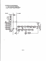
POWER SUPPLY CIRCUIT (Riparazione dei circuiti di alimentazione)
.
l.
Power is Not Turned ON (For models containing an AC power
...............5
supply).
"t"".'"""'
2. Power is Not Turned ON (For models with an external power supply)
3. Power is Not Turned ON (For models with a softnare sense type power switch)
.................8
'
4. Ths Voltage Cannot be Adiusted
9'
5. Example
l0
ll
l12
'.-r-/
6. Models That Can Use Two-wav Power Supplies (TS-71l, TS-81l,
....13
etc.)........
I
RECEPTION
1.
CIRCUIT
\
No Reception (No
Noise)r,........i.........
Thursday, December 25,
1997
.....15
9:57 PM
Page
ICE MANUALE RICETRASMITTENTI
Indice del Manuale
I of8
RTxk.nrood (in lingua inglese)
Pagine grafrche in formato .TIF prelevabili singolannente
Prelevando futte le pagine
C
possibile ricostruire il manuale originale
CONTENUTO
POWER SUPPLY CIRCUIT (Riparazione dei circuiti di alimentazione)
.
l.
Power is Not Turned ON (For models containing an AC power
...............5
supply).
"t"".'"""'
2. Power is Not Turned ON (For models with an external power supply)
3. Power is Not Turned ON (For models with a softnare sense type power switch)
.................8
'
4. Ths Voltage Cannot be Adiusted
9'
5. Example
l0
ll
l12
'.-r-/
6. Models That Can Use Two-wav Power Supplies (TS-71l, TS-81l,
....13
etc.)........
I
RECEPTION
1.
CIRCUIT
\
No Reception (No
Noise)r,........i.........
Thursday, December 25,
1997
.....15
9:57 PM
E INDICE MANUALE RICETRA,SMITTENTI
Page 2
16l17l
rslre
2. Sisnals
of8
af,e
Not Rec€ived (Noise is Output)
I
3. Receiver Sensitivitv is
Low........
...............22
4. The Reception Freque4gy- Fluctuates and The Reoeption Tone is
...........23
Wrons....
2.
'
5. Frequency Shift
25
6. The Reoeption Tone Breaks
.27
7. Receive Tone distortion
.27
8. The sound is low
.28
10. Cross Modulation
.29
Handv
Transceivers
I l. Mobile and
.
.............30
3r
Thursday, December 25, 1997
9:57 PM
"
INDICE IVIANUALE
RICETRA,SMITIENTI
Page 3 of 8
132
TRANSMISSION
CIRCUIT
l.
..................33
Transmission is
Impossible
........34
136
2. No Transmission Pow,er is Output (The ON-AIR Indioator
....37
Lights)....
2. Low Power (The ON-AIR Indicator
i. Lights)....
.......37
?..8
Thursday, Deoember 25, 1997
9:57 PM
(
"
INDICE IVIANUALE
RICETRASMITTENTI
Pase 4 of 8
ll. PRoc
(Processor)
................43
12. Transmission Tone O.ualitv is
Poor.......
................44
13. tlefective
PLL........
...............45
14. Power Fluctuation
45
15. Hiqh
Noise......
v.
......46
16. Mobile and Handv
Transceivers
.47
I
48149
.
DIGITAL CIRCTJIT
1. Display
Error.......
....50
2. How to Check The
Microcomputer
.......50
3. Nothing is Displayed
5l
ffi
.,.........,...
.........s2
5. Meaningless Displav or Displav
Error.......
6. Kevs are Not
Thursday, Dooember 25, 1997
9:57 PM
'
INDICE MANUALE
RICETRASMITTENTI
Page 5 of 8
Accepted
..........53
7. How to Find Missine (holes in a board, broken patterns, capacitors or
coils).....................55
8. Checkins Waveforms With the Power ON
9. Mobile and Handv
Transoeivers
..............57
PLL CIRCI.IIT
l.
PLL..
tv/
.......5
2.
Unlock..
........6D
3. How to Check the PLL Data Lines
. 0.....
............61
4. How to Cheok the PLL Data Lines
@..........
.............61
5. Tips for Repair (For Repairing
PLLs).....
..............62
6. DDS Direct Digital
\-
Slnthesizer)
............63
,.
7. Ts44o PLL
Ch*kp"i"ts-
.......64
8. TS440 Last Loop
Checkpoint............
................65
9. Quick Chart of PLL IC Input/Output
Pins........
Thursday, December
...........66
25,1997
9:57 PM
'
INDICE IvIANUALE
RICETRASMITENTI
Page 6 of 8
10. PLLs of Mobile and Handy
Transoeivers............
................67
AI-IXILTARY CIRCTJITS
l. Noise Blanker
2. Notch
Circuit....
......70
a
J.
Bo*Out
.\
\--r
................71
.............72
_
173
4. RF
Attenuator
5. Filter
, Swithcinq
.......7 5
6. Autbmatic Antenna Tuner
(AD.......
......76
SERVICE N{ANUAL
1. Reading the Servioe
-' )
Manual...
..............................80
2. Rules for Parts
Lists.......
......,........
........81
3.
Adiustnent
.............83
lM
Thursday, December
25,1997
9:57 PM
"<)
c
INDICE MAIIUALE
i
:
:
RICETRA,SMITTEI{TI
Page 7 of 8
T:i::: :i: ::Y :?::': :::
5. Functions
:
of
Commnents
.......85
86
I
87188
6. Rules for Naminii Terminds
......89
7. Reading Level
Diagrams
.........................:....
.........90
-
2. TS-950S/SD Final Transistor
4. TS-940
, Uplock.
....95
TS-790..:
ADDITIONAL INFORN{ATION 2
(Measuremept)
;
1. How to Estimab,the
Voltaei...
Thursday, Deqemb€r 25, 1997
............... ...........,96
l0:08 PM
.t
.
o
INDICE IvIANUALE RICETRA,SMITTENTI
Page 8
of8
2. How to Measure the Radio
Hieher).......;.... 1..... ....96
-Ailab4f
...
;.............. ;.....;.......,...-.... ;.. ;.......96
Spurious-
...........-.,..:............
......97
5. Ch€ok the Chrac$eristicsof-the Band-Pess Filter With the Spectrum Analwer
.
.:
9:57 PM
Thursday, December 25, 1997
wbu,
IJ-at,,n:J',;n
f eur*A,)ko*.&l
,
'
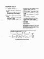
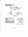
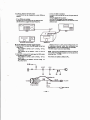
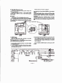
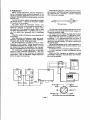
POWER SUPPLY URCUIT (Trouhleshooting the power supply clrcuitl
1,
Powsr is Not Tumed 0N
lFor modelg contriniry rn AC poryff supplyl
Setup ;Connect the AC power cord to the set.
4. Measure the output voltage of the diode bridge.
(DC.VM)
ls the DC voltage prosent? (G, Hl
YES :The diode bridge is
N0 : The bridge
1. Turn the power 0N and OFF quickly.
lf
Did the internal speaker buzz?
YES : The AC primary line is
fie
bddge is
0K.
Go to hem 5.
is defective.
shond, the f use at the AC primary
side blo',rs when the power turns 0N.
0K.
Go
to ttern 5.
N0:The AC line is defective.
Check the fuse at the AC primary side.
2. Open the case and maasure the AC voltage at the
primary side of the transformer with a testsr.
(Measure the voltage between A and B whh the AC
range of th€ tester.)
ls the AC vdhge present?
YES : The power swhch is
0K. Go to ltem 3.
N0 : The wire from the AC conDector to the
.
trans{ormer hes broken.
The power swirch may be defective,
3. Measure the rrolhge at the secon&ry side of the AC
transformer. (Measure the vohage between C and
D and between E and F with the AC range of the
tester.l
ls the vdtage pressnt at the AC secondary skle?
YES : The transforrrs is 0K. Go to ltem 4.
N0 : The wire at the secondary side of the
transforrner has broken.
5. Measure fie output voltage at the ouput terminalof
the AvR board,
Ercmples:TS-980, T$940 28F, TS-950 FHV)
ls the prescriborl rnttage ptessnt?
0K Go to ltem 6.
N0 : The AVR transistor is delective or the lead
connecting the AVR tnnsistorand the AVR board
YES : The AVR transistor is
has poor contact,
6. Measure output voltages, such as 15V, 12V, 8V, and
5V from the AVR board,
Are the correctvoltages output?
:lhe AVR board is 0K.
(The power is not turned 0N due to a problem in
YES
anofier boerd.)
Check l2V and 5V applied to fie conlrol board
and digid board. {ls the voltage applied to the
microoomputer or other lCsT)
N0:Ihe AVR board is defective,
Check the rear side of the AVR board for
soUering defects.
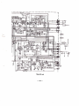
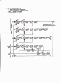
€izcto Dx4!t
tv
j'r
sw untt
llat.tat(Foot
(c,
o
r'
I
I
ai
t'o
POWER SUPFLY UN
0t
3a
130!.!(lt
et-l
Aa
;:
a3tt6rtc,
0
r,2
r5 lY)
0l
3C2att(Ot
03
23C
lr
arcrrallt,
2
IT(X43-I43O- OOI
o.l.a
o?
ol
Check points
(A) AC primary voltage Tl lN
(B) AC secondary wltage TlOUT
(Cll Hish B DIOUT
lC2) Common B
u
09l
xz-t2?
0ro
rsta0a
uz-tre
FOIIFlO-tl
sv-o3"
lDl) 28A 01. 02 emiters
(D2I28B FUSEOUT
03 emitter
(E) 21C
03 collector
TS-gl0 AVR unit
: t?-225
-
2.
Powcr ie Not Turned ON
lFor modrb rvldr an ortcmd powlr supplyf
3, Open the case and msasure \olt€g€s lSB. CB, 8C,
Connect the erternal powsr supply lo the set with a
DC powar cord. (The ponor supply should heve an
arrfilgrer and a currqnt-{imiting circuit.}
The iimit cuilent should be set to 3 to 5A.
8R, 5C. etc )
Are all thc voltages conect?
YES : The po\,ver supply circuir is OK.
NO: Check th€ pourer line.
1. The pointor ol ths ammeter on thc power suppfu
doEs not mon when rhe gollwr swrtch on th€ set is
rurned OFF.
YES : Turn the set ON- Go !o ltcm 2.
Check t:fie wltagcs lnput to ahe lF end RF boards. lf
dny of them eft i/l.caftect, chect th€ line on th'
povwr supply boad. ltthe voltaga Is stlll lrvofiac/,
the powar guppty bosr.t is dafactlvc. f tha voncgc
Is coficct, thero is a problem belwcen tha powe(
suwty board and thc f,rut d'tr,*polnL
revsrsoconnestion prevention diode is broken.
The povrar line mEy b€ dirsctvgrouMed Ou6 to
wire seizure),
4, The poyvar supply circuit F OK, but ths po,wer is not
turned ON.
The <tisplay cirauit is defective and the pilor l6mp is
2. Does the ammeter pointer movs when the pora€r is
broken.
Check the loltsgto et both ends of the pilor lamp.
Check the voltege of the DC-OC @nvener in th€
NO : The final transistor. gower module. or
tumed ON?
YES : The DC cprd fuse is OK. (lf the pilot hmp
lbhB. the vohage has been applied to the set.)
NO : Has the fuse blown?
Conccptual dblram
-? -
dbdrycircuit.
otpowff lha
3, Ponrcr
L Not Tumcd ON
lFormodchwlilt
a
rdrvor crrrclypo powrrrwidtl
Exarnples: Tl+27, TH47,
T
H-77, TH-2A, TH-4E TH-
78, TM-711. TM-742. TM-732, TS.50 lReceivers
3. Open th€ case and check whether the vottiage is
applied to ths microcomputer.
(Measure the voltage betwesn the microcomputer
Vct and GND, using a DC-VM.)
ls the \/olt8ge pGsentT
YES ; Tha SB line. fus€, and F,ower cord arc OK.
Go to ltem 4.
NO r Check tho SB line, fuse, power cord. and
conn€ctor.
contarnang timers, such es B€(XXI)
Setup : Connect the power cord (batter9 to th€ 6ot.
l.
'
B€s€t
How to.eset HF transceivers. includiog TS€0
Hold down the AFB kBy and tum the powe. ON. (All
resetl
Hold down the A/B key and turn th€ polver ON.
4. Check the line from the power switch to the
microcomputer
Does the CPU pon go HIGH whcn tho power switch
is preeeedT
(\trO reser)
.
l-low to r€set nrobile transceivers. such as Ttvt742
l-loH doryn the MR key and turn the power ON. {All
res€t)
Hots down ihs VFO key and lurn the power ON.
\--
(VFO resEd
.
How to r€sst hsndy trsnscaiv€rs
Hokl do\,vn lh€ M l(oy anct turn the power ON. (All
resetl
TH-28, TH48, and TH-78
Hold clcwn tha F koy and turn th6 por,wr
5. Disconnect the lithium battery for microcompwer
backup from the bord to discharge the bactup l;n€
and reset the m'rcrocomputsr. (Hardware r€set)
. Undug lhe povrrer cable.
.@ Ramwe the lithium battery. (Unplug thc pow€r
ON. (VFO
resetl
.
cable.l
-
(p This line does not dlsclnrge soon, Ground the
.
line by using a lead.
Connest the power cable and reset.
TH-27, TH-47, and TH-77
Hob <bwn the ENT key and turn th€ powsr ON.
MFO reset)
This is e 'softwere res€tting' procodure for the
mnrocomputer,
2. Dissonnect rhe power connector (b€ltory), hold
down th€ .ppropriate teset kay snd lhe power
switch. and connect the pour€r clnnoctor batrery).
For mod.b wilh so/fo,pre &a8 tln pow.t ewitr;h,
the mlcrocomputet is sctirn whila the pwar supply
ls connecTed. lf the powar ls tumod OFF whrlc the
microcomputer ia malfunctlonlng,
il
eile'E- ths
D!,ckup moda end romelnc tn !'[,e abno?met etete.
Tlprcfore, ?he mlcrocompu?at doas not t@cpa any
commcnd to turn fia pvter ON,
The chedt in ltam 2 ic aalrformcd to shut down the
powct completcly, tnd to stop tod ta.tct ?hc
microcomputcr.
6. Does th€ microcomputer output clocks?
{Check the microcornputer clock input wavefotm
with an oscillosopa.l
YES : The crystal oscrll€tor is OK. Go to ltem 7.
NO : lsa vohage epdied tethe lead of the crystal
oscilletorT
lf
voltagc is opplied to the lead of the cryslal
oeelllator. but clocke drc not generetod, the
osdllator or microcf.mputct may be faulty.
If no vothge la appliad to tha leed check whother
thc vonegc B agplied lo thc power lnput plf's of the
mtcrocomputer. There are two ar three power
lnput plnt.
ll no vohegc ls prcsont rt tfidsr
microcompnter.
-t-
plos, rcplsce
ahe
Feplace the boerd
As shown in the circuir di6gram. the grouncl pin of
th€ mic.ocomput6. is not directly grounded, but is
grounded through a lOohm r€sisto,. lf the resistor
ig broken, the ground pin is not grounded, so tre
micr@mpuror nelfunctions. Before reDlaciog rhe
board, check this resistor
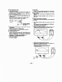
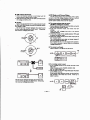
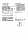
1LTho Voltage Gannot be Adiuctcd
Th3 AVR un[ contains a circuil thst generstes the
refer€nce vohage. which can be a{usted by turning
semi-fixed rrariable resistor (VRl.
The AVR circuit of the TS-940 is shown betorar
Wh6n the voltage€diustiflg variable resisror VRt is
turned. thg bose and collector voltagos of 02 change.
The base oncl collector voltaEes ol 01 chang€. The
baso voltages ol 0101 and 0102 change- The eminer
voltages of 0101 and 0102 are determined.
: ElLrtct
Qt
Ctaa : tlca.lalv)
: e6ctrtttYt
el
: lacttttrot
ca
Or,trn-rl:UOAI
: lz- st9
: rrl ttJC
{ru rlJa
: rata!!
c3.t
D!
oa
oa
a
:
tvotl!
s
Dr : lrtraJc {
rrz Sarl
Dl : rl:t.rJr t
tr: a.aJc
ora : ItlalJo TYT..JI
TS-9/O Al/B unh
_g_
I
I Thc output volt.i. ot th. th?a..tarmanrl
Th. volbgo o[ FB lllnrl Bl b hlgh or low
1. ls the Clz emitter vottage correct2
mgulotor b hlgh or bw
1, ls the input voltage of the three-tsrrninal regulator
YES : Drl, D5, €nd D6 are OK.
NO r D4. D5, or
broken. The
RG
DO
HIGH (orLOW}?
Normol: The lC is d€fec'tiv€
is shorted or a wire has
orth€ load is LOW (or
HlGHl. Goto ltem 2.
Abnormal : A circuil prior to the lC input is
wire is broken.
2, ls the 01 collsctor voltege corroct?
YES : D3 and 01 ere OK.
defective
NO : Check D3 and 01.
2. Firsr, red8ce the lC.
3- fue rhe Rl and R2 resistances conect?
YES : Ql01 0r Or02 is defestive,
NQ : The R'l or R2 wire has broken. (Rl and R2
are tias resistors lor Ol01 6nd 01 02.1
The TS-940 i9 lak€n 8s sn sxamde in the above
dessiption, but lt is the same tor other modeb,
lt the ploblem persists, the
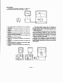
5.Exrmflc
gee the TS€40 AVR circuit cliagrEm again (Page 9).
I
voltage dctorminttion. 6iae dcteminttioo
ancl AV'R
lf th€ voltage becom€s normal when a pin is
tranelston
disconnected, the b6d on the pin is abnormal.
I
Thc voltrgo d zaB, tOA lr hlgh or law
1.ls ths rener diods (D14 or D9) for
ll tho FlOl oulfot la lnconcct
Disconnect CNg flCl01 outputr.
lf the lC orJtput becomeG norrrral. th€ load is wrong.
Discronnecttle 5V output pins of CNO one at a tim€-
Moet mcd,elt can b repalred bv chec*lng the btag
td€'lstanaas of tha AVR transistot zcnor diod. for
trcntistor,
load mey be
0bnormal.
voltage
.
d€t€rmin€tbn shortocl?
lf one of rhe diodes is shorted. the ouiput go€s
L
b broken. th€ output goas HIGH.
In either case, b€ sure lo check the output
ll the diode wire
transistor b€csus€ it rnay be darnaged.
.
lf the voltaeo ls HIGH
Measure the voitros at the pin. (DC-VM)
Normally, the vohage is 0V or less. lf ir is higher than
the lC output it is the caus€ of tho ploble.n
lf tho voltage ls low
Measure th€ tesistanco at th6 pin. lTester. ohm
range)
It must be lower than th€ resistances of the other
pins.
This ls the cBuse of lh€ problem.
-t0-
!
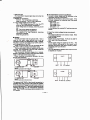
l.
Errmplo t
Disaorin€ct 6ll CN-A connestors.
2. Dbconnect all CN-A pins one at a tirn€.
3. CN-Apin 1 is tound to befaulty. R€conn€c(the pins.
4. Disconnect CN-B pin 1. lf the voltoge becomes
nonnal, this line is defective.
5. Reconnect CN-B pin 1.
6. Disconneet the CN{
7. This indicates tfiat the CN{ board is defective.
th. lloc b !.oundcd, ulr Jr o'ftmrrtr.
ll th. yohlga a. lbnolrnal, usa r D{C.VI,
It
O mst€r
I E[rnpL 2: Ttt-9ilo RF unh
!t!
Remove the co.nponent! on the boord onc
timc
in the same wEy and ch€ck thcm. (So6cr thom tgEin
5. Removc L3 and L4
again.
-r
No change
{
Solder them
after ohecking,)
6. Bcmoc R14:l ard Blil4 -+ The vohcAe becomes
Symptom: l8V is lower than the prescribed value.
7. Solder Rltl3l -r The wltage rcmains nor.nrl.
8. Soklor Rl44 -+ Thc voltlgB drops + This line
nonnel.
Cause: D48 is shorrsd.
1. Remove L85 --r No chaqgo -+ Solder it agoin.
2. Renrove L47 -+ No change + Solder it sgtin,
3. Rernove R60 antl R150 --r No change + Solder
them again.
4
RernovE R24,
Solder them
m7, VFl.
4ain.
and C77
+
No chang€
-)
-tt-
9
defieetive.
b
Removc lcl pin 16, C17E, D48, D25,end R152.
10. Solder the oomponents egain on€ at a time to find
th€ on€ that redrrces the wttaoe.
11. D48 is found to ba shoned.
See th€ circuh disqram on the next page.
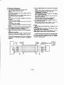
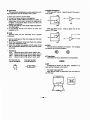
6. Modclr That Crn Urc Two.ryay Porrcr Supplloc
(TS-711,TS€11, ote.l
These models have the follotting configuration:
DC IN
To
I
rlch bolrd
Swltdr by connaolo.s
Powor St t
,\_
1. The AC po,ver is suppli€d. but DC power is not
sudied
The parts enclosed bv
1ff3
seem to be defecriye.
2. The OC pow€r is eepplied. but AC powcr
supdi€d
B not
'
How to idontlfy e defective thermistor
Warm th€ thermistor to th€ temperature at which
the fan moror siarts running,
Thsre ere two t!€€s of motor driv€ circuits
A 1ypc : lf the motor ground voltaga drops, the
datection circuit is OK.
The motor rs considered dafectivo.
tr=
The pene onclosed bV
may b€ defeaiva
See the 'Power is not turned ON' g.ction.
Fora two-waypowdr supply, chdck AC or DC powcr
to isolate the defea.
lf
neithcr AC nor DC power is euwilod. s ctcult
followlng DCJN le euspectcd.
B tyge : Unplug the connoctor end measure the
voltag€ at the positive (+) side ol the motor. tf Vcc is
present, the detection circuit is oK. The rnotof is
considered defecriw.
A type
I
The Al/F gat occerlvely lrot
The AVR transistor normally gats very hor. So it
us€s a h€at sink to dissip€t€ heat. but it rna!'gt€t too
hot to touch the hear sink.
.
Chock the coollng fan opcratlon (lf anyl
Wa,m the th6rrnistor (THl with 6 dryer or sold€rirE
lfon.
lf the fan runs. th€ cooling tan ls OK.
lf not, the rnobror the tempen ture det€ction circuit
is defective.
From lho
lcmparttu,a
datactloa daqrh
B type
F om
th.
ttrnpafduna
datrction citcult
-13-
.
Exrrplc
Touch the lrun8lstors or lcs fo land tho hotlo:t one
lf you find a componcnt thal becomes exogssi\rely
hot, the ]ord on rhe oJrput from th€t component is
ax@ssve. (Ovsrcurr€no See page r0.
AVR ransistor leods of rhe lS€40 (The cornponent
legds are connectcd directty to the leod wir€s.)
Check the mini+onn€ctgrs for p@r contact.
T9940 Olqt threetin c(xrn€ctor
lf e thtee-pin conn€ctor is used to connect
ff the AVn cirauft or the flnal clrcult le repalrad,
choc* tha cootlng ifan. Thic ls an importont ttp fot
mloimbing redundanl
tlangisto{ le9ds. remove tho conngctor€nd solder
rhe lords direotly to the pins.
Redrce ths AVR transistor.
lroigchY,,
I
A trnd3lof ln thr AVR ohoult lrllr
Meny engineers problbly haw experiencing tinding
a detectiw tansBtor and rcdacing it whh a new one.
th€t elso feihd wlun the po!^r€r w6s turned ON.
l.
Measure the l€sasEnce betu€€n lh€ outFUt pettem
lGNDl.
ol the tnrnsistor that failed and th€ ground
(Tester:ohmxl
ls it gulnded?
renge)
2. ls tte zener dbde shorted?
3
Check whalher lhe trensistor fails ctue to rn
abnormal locd or e defective AVR circuit.
Renwe the loeds. lFB. 28C, loc. 8C, 5C, otc.l
lf the tranli3tor fails .g6in, the AVB circuit
is
delective,
lf ft (bes not ta'd plug h rh€ oonnectcs again. one
rt
atime- Seefgq
11
4. lf the AVB circuit sc€ms @ be ctef€ctive, desolder
and solder the AVB boad components rgain.
Pult E ry soldecd leacls.
-
ta-
NECEPT,ON C'NCUIT
Stup;
SOL-VR:
MlN,
I
RF GAIN-VR: MAX,
1. Does rh9 beep sound whsn ttle rnod€ ls changed?
(For models containing the rnodo.announce
lunct'ronl
YES : The AF Power amplifier is OK.
NO : The AF poarer amplilier docs not \,vork, or
i
circuit tollq^ring the AF rmOlifier b dcfectiw
is always
5. The modc changc circuit or AF notch circuit is
defective, (For modols containing .n AF norch
. Apply a lsrge inout l60dBl lrorn the SG to check thg
$
conlact.
4, The muts circuit or squelch circuit
r..rorking-
1.No Rccrpnlon lNo Noisrl
'1
Podblr ourar ln drq{tr rftcr thr dclrction ctrgo
The ext€rnal phone jack or headphona iack has a
poor oont€Ct. A speakor wire has broken.
2. Th6 AF amplifier is dcf€sttve. No bias is applied to
rhe lc.
3. Th€ AF-Vh ls defective. The connecto( has a poor
l.
ANT: To SG, AF-VR: 10:00
meter.
The meter ope(ates: The rsceivgr ci.cuit is
working normally. A circuit lollowing the
detection circuit is d€fective.
The mot€r does not olxr€te: Tho r€c€ivor circuit
iE nor working normally. See page 19.
circuit)
6. Broken D3ttern. poor soldering, ot poot cpnnector
contact is Dr€sent in the ebov€ circuitg.
! It th. rrodvr clrcrrh lr OK rtcck r fallows:
(A drult bllqrfrn tlro drtrdon nrgo b dolralvcl
. Example: T8-4/ro lF unit (SGo next p.g€)
'1. Touch
Jl t -SPK- lThs AF-VF must b€ set to about
l0:ffi.)
2. T@ch J4-SPO.
3. Touch J2-4F2,
4. Touch J2-AF3.
6. Touch the 012 base.
6. Touch lcl pin t.
Cheok lhe eibow poinrs ao
ctoas n6 sound.
lbd c polnt
where e
buz
For exempte,lf a buzzaoundawhenSfr ia touched,
edd
lt
doas not when AF2 ls touched, lhe circuit
betw€8ln thaEc polnti ie
AFgly tha taatar prob. le tho tcu? poirra ghhln tha ghm rr rtlr lxtOOOl io dract
ch€c* thc polnrr ln lhr ordor ahown bclow.
(You crn ure rn ooillorooga to ciack whathat a nolt' lr outgol'l
(D@
@
ll tho rcCclvcr drcult lr OIC drccl rr iollonrs
-
t5-
dcf*tive.
wltcttcr t bu:t 3cund!.
o
I
How to chccl thc SOL cLcuh
1. Check the SOL volume.
lf th6 SOL-VR 's OK, the SOL circuit is do{ective.
I
.
The microcomputer outputs it when one mode
Howto chcck mutlog
The mute signal is output to cur off pop noise when
one mode i3 chaog€d to onother or also 1o turn thc AF
signal OFF during transmisgon.
TS-040, TS+59. T96Sn. TS€50. TS-790, TS5O. etc.
ts
changed to snother,
6
o
The D(B or RL Eignsl is received during transmission.
Check the input to lhe mutng transisror or lC in rh€
AF lina before the AF-VR.
SOL MIN
00-600(r
.
sor MAx
2. Feplace the lC.
3. ls the resismnce of the resistor connected to the
output @rrsct? ls the capecitor shoned?
4, Chock th€ resistors and c€pacitors of the negative
10I(l-1mko
reiurn circuit.
TS€40, TS"950. T$950SDX
-:i
The AF povwr amdmsr do6s not work
1. Check rhe Vcc line voltage with the DC-VM.
5. Check th€ voltage of the input terminal. ll it is
abnormal. desolder all the connected pars and
sold€r them ag€in to locato the defective cirGrit.
fnsoLM,N
V)
I lVlododnngpdrcuh
o{I
There are trwo typ€s of mode*hange circuiB: one
that chcngcs rhe mode with a diode and another that
ch6ng.s h whh an lC switch,
2. Messure the SSO ling,roltaga using the DCI/M, end
turn lhe SOL-VB from MIN to MAX.
Doas the vohogo chenge?
It it doss, thc line is OK.
3. Measure th€ bas6 voltage of the transistgr that
mutes th€ AF lins. and then lurn the SOL-VB from
MIN to MAX.
Doqs the t oltEgg changel
It is OK if the voltags f,owing bcnveon the b6se
snd emitter of the transistor is 0.6 V or less when
the SOL-VB ie sct to MlN. or if it is highor rh6n the
vohage lO.6Vl that con tu(n the transistor ON
wh€n the soL-vR is sct to MAX.
More accurately, if the vottage chengas, ThO AF
mute irentittor mey be defective.
If lt does not change. checr, the vottage of tho
Neceditg clrcult by chenging the SOL-y8.
-17
The TS-14O circuit d-ngom from the detection circuit
to SPOUT ig shown on the nexi 9rge,
The TS-140 SQL is effectivs in FM only, and O58 is
turned ON and OFF by the vdtage at lC6 pin 13.
The mute signal rnak€s CN3 pin 9, MUT, HIGH, and
mssos through D70 to conlrol Q57.
ln transmil mode, CN3 pin '14, BB. and Q43 OUT 9o
HIGH tosonrolDllz and O57. {ln SSB mode. TXB
and O55 input go HIGH, the o{'tput goes LOW, and lC7
(2/4) tums OFF.)
f he mod+changs circuins changed by lC7 in AM {4/
41,
ssB
w4\8N
FM (3/4'.
AM modo: lC7 pln 12 gocr HIGH,
rnd tho odla; prns go LOVi/.
SSB modc; lGl pin 5 gocs t{lGl{,
snd
thr odrir pins go
LcnA,
FM modo: lC7 pln 6 goes HIGX,
rnd the oilr6r Dlnr 90 Ldl,
Circuh rre
lile rhis.
Thc TS.llo cbcuh dlrgnm lrom toro dctrstl'on drcrrit to SPOUT
-
lt-
\l)
I
.
lf r du{t plor to fi. ffion drqdt le d.r.saho
Examplcs of typical probtems
1. CAF is not iflDut ro the detectbn ci.cuir.
No noiss 'rs output i.r SSB onty. OK in FM end Alvl.)
tJse an oscilfoscop€ to chec* thern.
CAR
8AI
8$E drtocdon cfocrrft
2. &YB ls not supplicrt ro the roceiver tF stage. (SSB.
FM. Af,4I
Chcck the
rransigtar,
udt€e of ttre
3. Delactlve AGC
Chcck tho rclreg€ ol th6 durl.gpte FET to whach
AGC i! apdled.
ilfXB
let*€.. i? is
wc
rocaiver circuit FET or
Bir3
7-gV
AGG or
1-2V
MII Fl
lnput
t-2v
2-3rt
Modd ndth common
I
ot gV.
tV or tgv during tnnsmlscion, bul
ll comnrcn
-19-
E ls
tsv, vCC b.r,omcr
lW
o?
highar.
2 Slgndr rre llot
1. lnput a 10OdBg signal from rh€ SSG ro rhe anrennE.
Does the transcailer receiv€ it?
Roodved (Noha ls Outgutl
Set frequeocy: 14.100MH2, USB mode
YES : The signal line is broken or tho mixture level
SSG frequency: 14.101MHz
is wrong.
NO : The mixturc frequcncy
frcquency ie wrgng.
Point LO2 Polft
Pol.lt LOr Folnt
co
AB
Make..iig like this
The capecltor is used for DC cuning.
Uta.
i! incorrcct
Polnl LO3 Polnt
EF
capacitor
with hl$ capeitrnca so th6t it mty be used for HF
to UHF.
Gr{o
ctnnad to GND otlh! !Gt.
ToSSG+
The elligalor clip doas not provide sufficient
grounding. See the ligure below to bensr
undsrstand the connetbn.
-2O-
The pLL
3. Connoct lhe SSG to the jig and input signals to each
poinL (Fix th€ set frequ€nqy to l4.lOOMHZ.)
Thg sot lF frequencies ere as f,olkcws:
l str 73.O5MH!; 2nd: 8.83MHz; 3rd: 456kHz,
Point Ar r4.lOlMH? (SSG frequencl, about
(SSG
ls
fie
outputl
signal
I
lOdB
received?
defective'
Check conneclions from the antenna to point A,
RF amplifis power supply, ond th6 BPF switch.
How to cllculrtc LO-t, LO{, rld LO€ frrcprncl$
SupposE thar lhe lrequencies ar€ as follovvs:
S€t dispby fr€quency : l4.lOMHz
First lF frequenca : 73.05MH2
Secorrd lF frequency: 8.&lMHz
Third lF trequ€ncy:455kHz
1- LO-l
YES : The BF band-pess liher (BPF) is
73 05
73.O5
-
14 10
-
58.95MH2
+ 14.10 = 87.15MH:
LG'l must
be onc of the abovo frequenc'os.
NO i Other circuits are defective.
2. Lo-2
1@B
Point B: 73,05MH2. about
ls the signal
YES : The Lc},l lrequenry is
r€c€ived7
73,05 - 833 = O0.22MHz
73.05 + 8.fX! - E1'88MHz
LO-2 must be one ol the above frequencies.
incorrea.
ls rhe t-O-l frequency cotrect? ls the level
sufficientl
deleotiw.
point C: ?3O5MHa about 25dB
3. LO3
6.83
NO : Other circuits are
-
0-455 = 8.375MH2
8.83 + 0.455 = 9.285M1'lz
LG3 must be one of the ebove irequencies.
ls the signal rec€iv€d?
YES : The tirst boadfass liher (BPF) is
or the first lF amplifier does not
ThEre is a problem b€tween proints B and
Locrt€ it with rhe
NO : Other circuits'.re
defeciiv€ t tr th. lF frrqrnoy b dffttotlt
Sct cl3dtY trequerlcry : 14 175 MHz
wotk.
FirstlFtr€qu€ncY:40.055MH2
C.
jig
S€cood lF fteguencl : 10 7 MHz
dcfcctivc.
I LO1
40.055 - 14.r 75 = 25'88MHz
Polnt O: 8.8ilMHz. about 25cts
40.056 + 14'173 - 54 23tt'llHz
Is th€ s'rgnal receivedT
LO-l mu3t be one of the lbov€ freguencics,
YES : Tha LG2 frequenry'rs iocorrecr.
ls the LO-2 frequency correctl ls the level
2. Lo2
sufficientT
40.055 - 10.7 = 29-355M1{z
NO : Other circuits are defsclir/a.
aO.055 + 10.7 = 50.755M1'lz
LO-2 must be one of the above frequencies.
Point E: E.€tilMHz, about 40dB
ls the signal received?
YES : The second lF tilter or the second lF
ampll{ier is deiedive.
There is a problem between points D snd
E.
Check it with the iig, The NB gate rnay b€ closed
lf so. check the NB circuh.
NO : Other circuits Bre defective
Point F: 455kHz. 40 to 6OdB
ls the signEl received?
YES : Ths LO€ frequencry is anaorecr,
ls th€ LO-3 fraquency correct? ls the lsvel
sufficient?
NO : Other circuils are dafectlve.
Ch€ck th€ lF fiher change crrcuit or tha third lF
amplifier.
--21 -
I
Errrngb:l$SO8Dl(
Supposc that the AF unh or lCl 1 b defective and ttre
H642 frequcncy is incorrect.
t
- tnpur thc 1oOdgr tenal to thc antcnna- --r NG
lnput the aignal from the RX-A tTlN te,minal on the
2
rear
ol thc unir. l2odBd
4
NG
3. lnput th. rignal to RF unit TP-3. + NG
4. Inputtlr3 73-G5MHz. zod8rreignelbthc RF unitCN.
7. MlF. + NG
5. lnput the 3ipal 6lF unit TP€. + NG
6, lnput lhc 8.83MH2. 50dBu spnat to TP€.
Receptlon b€gins ar thb tlmo. lf lha signol is not
reeivcd before being mixed, but 6 received aftcr
mixing. the sign€l is not beiog maxed properly.
7. Check ths H642 frequency with 8 frequenca
counttr.
8. h is fqrld $at tre H042
9. Ihe VFO2 in thc AF unh
10. Sse
'11
Recoivrl S.mithrity 1r low
Us€ a ssnoifvity check ib.
Use another set that can be usecl for corrparison, il
any. to find a problem.
lf the sensitivity is lower than SdB, it is diffrun to fird
thc problsrn without using a set for cornparison.
lf $rch a sst is not avaibbte.
referring to the l€\r€l diagram
by
c€
Manual. lThe tevel diagram shoutd be used for
intonnation only. The manuel sho\,vs the values of the
des'tgn samdes and pr€-ploduced sefs. Th6 des'En
and the lot€l diagrarn may be cheng€d durirlg mass
production,l
Tho levcl diagram is explaincd in dctail in the
'Rccding t'he gcr\racc mlnurl' sec,tion on page 90.
wrong.
taking the TS€6i0 as ao erompto.
tie
, lCl 1 is
3.
PLL roubleshootang s€ction.
iound to bo del€stiv€.
-22-
!-(
j
4.Thc Rocrgalon Fngonoy Errfudot.nd
Thc Reocption Tonc irUlhong
f Thr rrcrfion nooo ftrch,tnr h 3gB
Thor6 is a possibilityol g)% or h[her the PLL bck is
not sta6le.
Eeder to rhe PLL unlock sect'on.
a T.cinh0.lcrfrd&t3 . proUtm
Apfly dtc ccl$oecope p.obe to the adirrsting points
ftr tm
.
PLL lock vohage and obsen c
$o $r!r€idm.
Occillrorcopc sotup
VOLT/DM: f\,lardlrxm scnsitivity.
lnprrt AC. TIME/D|V: Ahout trE
NG
1. ll all the tcsr poirit! are OK:
Check fhc lC UL detgction tcrminet in rhe gsrne way.
-
2. It the UL detection t€rminal is OK:
Th€ terminal can be chccked by using SSGs as
lf only one SSG is availabte:
Connect a dummy lo€d to the set that oan rransmit
lollows:
signals.
Transmit sigrnalg tt low @r^rer.
Use tt€ SSG to supply the bcal f(oquency.
Connect e slmplllled antenna to th€ anrenn! of rh€
delecrive set.
. f t\n o SSGs gre a\railable:
Conncct one to th€ antenna of the defscdve set.
Use the olh€r to slppFy the bcal frequancy.
Daftctiva
f t t Or. dllrctivt r.6lvor rrcolvc rlgmalr
t Remove LGl and input the SSG carier ro th€ first
nixer ckcuit.
2
Tha probbrn is solved ; LO-l is wrong. To PLL
circuit LO.1
Thc problem as not solvod ; LO-2 or LO-3 is
wrong.
lmtall LO-'r, remove LG2. and input th€ SSG carrier
to thg s€cond mixer circuit.
The probbm is solved I LG2 is wrong. To PLL
circuit LG2
The problem is not sohrcd ; LG3 is wrong. To
PLL circuit LO-3
l.l
M€asure the LO-l, LO-2, and LO-3 frequencies with
ar6
disconnact€d. ln$rt the frequencies into th€ SSG.
The SSG outgut must be at least StldBI.
a froquency counter wh€n the connectors
Noic : lf the circuit ls conltgured as follows, k cloes not
work unless the voltage is applied to the hot side of the
shielding wire. fi$7901
This chock can isolato a detective PLL.
To LO lN
To 8V lanc
-2+-
I
1
2.
tr you find c ddcctlvr PLL
Replace the VCO transistor and FET.
Replace U€ varh,ap diod€.
lf thc velua measurcd with the lrequency ct untet
eguals tha calculated vatue wlthin t2kHz, it is OK.
lTha local tregucncics shifr tn some modes-)
:tSto 5 kHz shift: Suspastad. Check it.
xO kHt or more: Chcck the PLL circutt.
circuh.
See the PLL circuit section.
3. lf ths model is designed to adlust the lock voltage
with a trammer, reploce the trirnrngr.
4. Replace the smoothing ceFr€citor in the PLL tPF
5. Replcce ths trarsistor and lC in ths PLL LPF circuit.
6. Replace fic PLL lC.
You can tolvo thc ptla.blcm Jn thlc wey wi?h
ponldffr/ry o( gn tcr then 60%.
tf theVCO la modularized, raprecr
tdi,e
l{olo
: The old rnodels use cry$al oscill€tors. Reacliust
aach frequency as instructed in rhe Service Manual.
a
module.
I
|tthc plobhm riln prrslsrs, do lclolloup
L Apply cold spray to each PLL component
during
rec€gtion.
Cool onlv one component and observe it until it goee
bock to th€ norflrsl temp€ntute.
Continue this proclss until lou lird a component
th6t worsgns or irnprwes the sy'ptqr.
2. Approach a hoi sold€ring iron to e8ch componsnt,
and p€rform a check in the 8€m9 way.
5. Frequency
Shilt
lBoth th. trenrmisrion rnd rcclptlon f?oquancici mu3t bc chccktd bcr. bccoulr ftt ll
ncc.|arry to drternrlno ndfielr her rhlftod, tho
tnn3mhsion or recrption frsqwncy.l
I
Chcck
lhr tr.nrmagrlon ond rcc.ption fr.-
qurndrcfor dlrphy
1. Both lhe transmission and recspt.lon lrequencies
have shifted sgually in the same dir€stion.
The PLL relerence frequency has shiftBd.
2. Only the trensmission fr€quoncy has shifted.
One of the locsl frequencies has shitted.
Cabulate th€ trcel frequencies ILO-I, LO-2, and
LO-3t.
Sct displ€y: 14.0fl1 MHz. Mode: CVV
lF frequenoy: Firstl 73.05MH2; Secondr 8.8€MHz;
Third:455kHz
t
LG1
73.05
LOZ
73.05 +
to3
8.srro4s6
14.(X) = 87.05xxxn
8.83
-
etO0lt
rlo0fr
Each oscillator hag a elight error as ghown abo/e,
but if ii is edded to or doublcd, th€ frequency shift may
b€co.no s[nif-rcant,
I
Th.trtunlrlboficqocncy dtlftr ln Fill modronly
(TS??0, TrSi- ?80, TS-7 t 1 , T$81 I . T$790, otc.l
The old models us€ cry3lal qscillators in HETs for
freguency moduhr'on in FM mode.
1 Veriry that the transmission frequency does not shift
in C1,v mode.
that rh€ r,ansmission frequency shilts in FM
mode onty.
3. Find tho varicap diode lor fieguency moduhton.
llt probauy ts locatcd in tlre lF unit.t
2 Verify
4. Adiust the freqvency
cpnnected to rhe diod€.
f
of th€ crystal oscillator
ffro nnqrnGy b oorilct ln hll modc only
The FM lrequenc.y nray have been adjustsd while
the Orr/ basicl lreguerrca hes shifted. Acljust the CW
fr€guency. then the FM frequency.
I
X
qrb $. roorprum ftr4nnory bs $ift.d h ff{ modt
ln SSB, i{ the fr€qu€nqlos sre cor€ct, only the
reception froquency nwcr shifts.
59.05xruo<
= 81 .99xxs
f
:tA#
Varfy drrt $rr trnrnrhrlon lroguoncy b comct
Check rhe PLL reference frequency.
On€ of th€ lwo values is oorrefi.
Ch€ck which frequsncy has shifted by calculating the
frequencies in this way.
-26)-
Check whether each mix lrequency is oorr€ct.
Thls sho$rs that lhe trensmh frequency is correct,
but the rrceive frequenq/ has shifted.
a Chd( how mudt ft. r.c.ln
fia$roooy hrr
{dftrd
4.
f
an lc 13 us€d tor FM clet€ction:
Redace tho compgnents ln the orcler listect below:
SSG trequcnc.y: 29 SO0OMHz
SSG MOD frequcncy: lkHz; DEV: 3kHz; MOD; ON
tc
Set freguency: 29.5(FOMHz
455 lF fftcr
-r Dircreto
coil
lC oscillator (hs frequency may
1. Shifi tho SSG frequency in lO0Hz units and find the
best SINAD point.
1l it is within +.l kllu, il rarles within the oomponents.
It can be impro\red to sorn€ degree bV foadiusting
ths lF.
2. ll it cannor b€ edjusred to witlrin tlkHz:
Check eacn LO fr@uencl shift during rsception.
(Ref€r to the transmbsion section.l
It each rrrsssured fiequeney equals the theoretical
frequenc"y t2kHz. th€ro is no problem.
lf h is greater. pedorm troubleshoofing as descrabed
in the transmission section
3. Each lrequency is conect.
A comnrn caus€ is a pass band shift of rhe MCF
fiher.
Becausc tlre central lrqu€nc1, of the MGF filter has
shifted. il seems to [re an lF shift in FM mode.
shilt by t2kHz. bur ir
is permisslble.)
lF MCF fihar
5. A sensitMty check i[ mey be useful.
Example: 14.100MH2. MOD€: FM, SSG frequency:
.
'
.
.
.
.
14.1OOMHz: MOD frequenoy: 1 kHz: DEV: 3kHz
ln this case, do as follorw:
Apply the i'tg to pctint A, ard entar the lF frequency.
l455kHz, €OdBFl
Apph the io to point B. ard ent€r the lF frequency.
l465kHz,60ttsd
AppV the j'rg to pornt C. and enter the lF trequency.
(40.055MH2. 60dBB)
Apply the j'S ro poinr D, and enter the lF freguency.
(40 O55MHZ, 2odBFl
Apply th€ jig ro goint E, and 6ntor th€ lF frequsncy.
(40.056MH2, 20dBtr)
AppV th€ iig to pornt F. and enterthe FF frequency.
(14.100MH2, zOdBtd
You can ftrd the (bfectivo poft by checking the pdnt
whcre the fteguenoy begins to shift.
73.05MHr t.SlIUlHz
tt
L,,,i
t
I
t
,
I
I
Ylr?one
Co?7ccl
It thare is a problem p.ior to point D:
6.Thc Rcccptlon Tone Brceks
Does ths carrler or local signal break due to
1. Subject tha s6t to vibrstion.
The raceptbn tons breaks when the s€t is subiect€d
to vibration. -r The compononts have oot b€en
securev soldEred to me board. or conneclors have
poor contact.
2. Connsct an sxternal speaker and subject the sst to
vibrationT Point El
Does the AGC voltage fluctucteT lPoint Fl
Does any recagiliofl voltage. such as ER, ctange?
vrbratioo.
The reception tone breeks whEn the set is subjectod
to vibrarion. -+ Somc circuits before the €rternal
sp€6ke. rney be detective.
3. Subi€ct th€ set to vibration while observirp the Smeter lB€ceive signsls at sbout S-9.)
Poinl
E
The S-meter lndicatlon changes largely due to
vibration. -+ The AGC or powe, supply circuit is
doleaive.
4. Whila subjccting the set to vibration, observe th€
wcvelorm !t €ach point from point A with an
ocilloscop€. (Oscilloscopa VOLTTDM: SOmV; lnputr
AC; Sweep time/div: 2na)
LO
LO
Tone Dbtortlon
7. Rcccivc
Check the pointg A to D in th9 same r,\€y.
a Pordbh
dctosts
1. Poor cootact of an external sp€ak€r End phone
2. Dclcctive AF gowar amdifier or AF.VR.
3. SOL gate, mute gple, or mode chaoge circuit
4. D€tuctivo DET diode or DET lC.
When checking $e diode, remor€ it lrom the bo6rd
and check
it in both lhe forwerd and reverse
directions.
D.f.ctlv!
lC
Defadlva lC
-zt -
Poo?
conttct
8.Thc Sound is Low
9.
1. ls thc sensitivity low?
tf SSG OUT is -6dBt and the VN €tio is todB, th€
sensitivity ic OK. lf the S/N rEtb is not 10dB. go to
the'Low sensrtivity' seotion.
Since lhe S-rn€tsr op€ftltes diflerenrly in SS8, ani.
and FM, the checkpoint depends on th€ rnods.
(Ercept
B€dnl
SSB and AM : The
2. Check the w€veform at tho posiriva sid€ ot the
9meter is operated W rh€ AGC
voltage.
internal speaker (lNT-SPl and GND with an
oecilloscqpe.
Does eny r/vov€torm gDpear at the posftive side?
Does any waveform appear at the GNDT
S-moter
FM : The $meter operat€s when the carrisr is
detscted.
I
Thr $nrrtrr doc not opcrltC
Obserue howthe S-meter pointer mo\res in SSB and
FM rtpdes,
A
,k
rt
eryrlotm .DporTr
lhe GNO whEn lhe
wlrcis oprn.
Chcck rhc AF linc prior to the AF-VR with .n
6cilblcopc.
f,ecdw th€
1. The S-mercr poinrer does not firovs st all in any
rnode.
The meter or the meter+hange circuit is defsave.
The connector has a poor contact.
2. Com€ct lhe tster as follorys;
B€ducs th9 Ohm range ftom xl(no to x1@ to xlo.
lf th€ $rn€r€r polnter rno\res, th€ meter is OK
SSG OUT20dBFeignal.
4. lf th€ AF oLrtput is 0 1 to 0 2Vpp, the line is OK.
A 8ANGE
r'l(Xl < rt0o
5. ls the RF-VR 3ctto MA)(?
6. ls rhe AGC line OK?
S€t th6 AGC line to about 3V when thcre is no
\
3ignal. (lt depends on the rylodel.t Ag the receptbn
signal strengthens. th€ voltage
of this
;N;
line
decraases. lt is linally reduced ro abour lV.
7, ls the CAF or LO s-rgnal lawl conrtT
CAR: 0.5 to 0.8Vep
LO: 0.4 to 1.OVpp
1
lf the rneter polntor doea nol movel
Meggure lhe registance between the positive (+)
side of the meter rnd the chassis.
lf it is zero. the S<ngter line ls grounded.
Rephce the mgtgr.
-n-
Thc S-mctet edjustmenr tn SSA ie E little
ts Instructed in
the Sanice Manuel.
lf the vtttEble resiator (or coil) used for t-l
ddlustment siifis cxcesslvely, the AF output or
2. With the power oN. apply the tesrer probs to points
1 to 5 in th'rs order. (Ohm range x100O)
lf the s-meter pginter does not rnove, this pcint may
complicated. Adjust the S-meter
b€ def€ctivo
Example: It the pointer mo/es at point 3, but does
not mot/e at point 4, th€ part between those points
sensitlvity may decraa*.
!s defective
lO. Cro*s Modulation
1l Remore the CNA and apply the tost€r prclbe ro
Advbe the use. to use the ATf or AIP switch.
The BPF-change ctiod€ for reception may have
the met€r side ol the CNA.
2l lnsrall the CNA. refirwe the CNB. end apgly the
tcster probe to the bo6rd side of rhe CNB.
O lnstall the CNB, retncwe the CND, and appty the
tesler probe to the board side of the CND.
4l lf the $meter pointer movea et this time, th€
falled, Check the diode.
PCB3 board is def€ctive.
I
'l
trtha mat r eo{r3 gff-tcab
lkth.
nF-oAlt{ vR
!.tto
MAxtt
. Change ro FM.
ls the rtreter reading reducedT
YES : Defective in SSB onlvNO : The entire S meter circuit is defective.
2. Tha meter is off-scale in SSB only.
Enter about signals 40dB to the antenna lrom the
lf the BPF3 shown in the €bove figure is rhe current
bsnd, only th€ BPF3 diode ghould turn ON and ths
otheE slDuld turn oFF lf rhe BPFS diode fails, the
signal passes through the BPF3 and BPFS. causing
crog: rnoduldion
SSG.
Are the signals receivedT (SSB)
YES ; Only the S meter circuh is defective.
NO : The AGC or powar suoply circuit is
d€lective.
Check the AGC
vdiage
Most s€ts balance the positive and negative
voltages of the AGC circuits. lf €ith€r rroltage is
absent, rhe meter goes oft€cal€.
3. The metsrgoe6 offscde in botfi modes.
Check tne RXB, common powsr supply voltagca
(such as 8C), and TXB.
lf lXB is ap,pliod during reception. the ALC. S1i/R.
PBOC. or Fr'VR lC meter mey rum ON So check
TXB.
-zg
*
11. lulobilc and Handy Tranrcclvcrc
ltlo round output (Ch.ck whh en ordllocoopcl
1 . Ch6c* whetherth€ lF lC OET ouEut Gonteins nois9.
2. tf ths lF unit is modularized. replace the rnodulb.
I
(lr contains th€ SOL circuit.l
3. lt nobo app€ars in
tFre lC output o. lF module BA,
chect the input and outgut of ths el€ctronic va,iabl6
resistor {VR),
ll the input is OK, but th6 output is NG, the
eleqBon-c variable resistor (Vn) tC
is defective. Data is lnpu to the cont(ol lin€.
Ch€ck the data line while turning rhe AF-VF,
It d.te is pro3ant. the lin€ is OK.
4. ls $c PLL unlocked?
Check the LD line of tho PLL module.
5. The dual-bond rmdels contain an lC thst swnches
the AF 3ignalB {MAIN and SUB}. Does it work
corrocrlyl
6. ls th€ TXB low?
orthe control line
TtU€41 porur ariGhlng clrcoit
f
Poor r.c.ptloo llow*nrhirhll
Perform troubleshooting with a iig. See pego 31.
The FF amplilier .t the first stag,e fuils mo8t often.
(Poor sensitivity of 10 to 20dBl
other,
.
,f O,
Reason whv
oftcn feils
th.
RF ampllfier st the firat
ilage
tronsrnined, forward bias is applierl
totnngmissbn/receptlon swhchirn diode Dl to turn it
ON. Diode D2 Oat protects th6 lirst r6ceptbn stgge
l/Vhen a sEnol
as
ON. Therefore, thc RF signal from th€
module is grounded by D2 and not-applied to RF
also lurns
amptifier O1.
-30 -
lf
no
bits is applied to Dl or D2 tor some rgason or
Dl or D2 is OFF as shown below (the dioOe
gorves as a capcchorl, RF powcr goes ro 01 and
d€stroyg it.
b dan"god, ool&r R egain.
futpld
Iathcfirstclogo mayfail duoto e problem
in dE arrnsmirarion clecuit, so vefitythat ell the lCg
In t.he f,rct etaCe work prcperty by Bpa.todtv
checking trcoamission end reception following
rePalr.
I
I
between goints D and C
Low mix le\€|, Defective MCF.
3, Defec{ susp€cted betwe€n points C and B
2. Detect susoected
Low ruecptlon rcnahlvlty
This input should provrcle SINAD 1zdB'
Def€ot is suspected after point D
lF loqal oscilletor lailure. Low oscillator level
Defective lF lC. Delectivc 455 lF fiher
€d3|r
EMF
l?dBF
EMF
@
Defective RF amplifier or helical BPF
4. Defect suspected betwEen poirns B and A
Defective LPF or switch (EL, aclctitional band, €tc.t
lvrm3 lHlgh-frequency WVMI
eoaEr.
eur
28
+
RF
I
STiP
DET OUT
aPf
Rccrtvrl lraqu.ncv t[ttft
See Paoe 25-
f
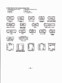
Odoriiv.9OL
See Page 17
I
cor.rTFoL
S-mltrr
lli
rF tN
To
soL
-31 -
PA
AF
VR
I
rnrhlvtty {wlth rn rddrional bcndl
Most rocent lransceivers have additional bandg
Low
(wide+and .€caiv€r circuilst. lf ths!, tail, (he ssnsitivity
d6t€rkyatos.
As shown in the below tigure, many switchlng diodes
aae connocted to the receivgr llne.
1 I D208: Tnnsmission/reception switching diode
21 D2Gl and D210: Recoiver stsge prorectior diodee
3t D21 l: Economiccl ktwgo,wer BF switch
q D214 end D215: Switching bewwen 36(MHz and
430MHz bande
ll any one ol them is short€d or rnaltunctions, the
sensitivity d€t€riorates.
n-nl O4GJatI O{rt
E
GERS
ffi
a
G
Dl{
ENE''I
=EL{_rt?" li
-!a-
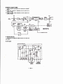
TRANSMISSION C'NCU'T
Setup ; Set En amarour band frequency.
Cooneet the ent€nnB of the s€t to a clummy load.
1. Press tho SEND or PTT swrtch.
Does ths SS line go LOWT
V€rify that the SS line becomes 0V or ths
miqocofiputer input pin.
Exrmplo olT5.o60
2
ls any voltage applied to the TXB on th€ lF or RF
3. Does the ransistor that controls the TXB gensretion
work propeiy?
board?
ll no \oltege is apptl€d to the TX8:
4. Ch€ct tho UL detection cirqrir voltage.
ls the transistor that generates TXB defoc(lve?
The transistors that procl.uca powcr supply vohagce
arc of 2SA or 2SE type. lhcy may lalt e*lly ll the
o,r$ua lc grounded. lJ a transistor hes feltd, chr,*
wheahor its output hes boan grovndcd be(orc
replacing the trenslstor. lf you omh th,s check,
msny tantistoro may feil.
Ouring recqption
TFX
tx59 -368O-Ott
oFF
ON
--
---
aol<!
TRX borrd
opcrdon
_E_
1.
TrenmircSon lr lmposiblc
7. ls any \olt€ge appli€d to the collector of O49?
The 8XB and TXB vollages are the same as tho
8. Ooes the base of O49 go LOWT
corhrnon powersupply volteg€ O$950: tSV, T$890r
8V, TH-28:5V)
8V is taken here bscause it is usd by many rnodels.l
1 Doesrh€
No
Y€s,
9. Q49 is clefective.
+g
TXB changeT
0V TX: 8V
2. Oossthe SSchsng€? RX:8V TX:0V
3. Doesth€ CSSchange? RX:5V TX:0V
RX:
IN-HIGH: Swltch turB OFF
IN'LOW: $ratch lu.ni ON
DTATY?E
4. Does the transistor that genomtes TXB work
properly?
NPN rransistor: Ths base goes HIGH,
PNP rransistor: Tha bas€ goes LOW,
5. Doss tha transistor lhat @nrols rh€ TX8 generation
uork properly?
tl it is modularized, check the CTXB,
6. Does lhe microcomputer issuc
inhibit request? fiXll
7.
r
?
ouT
v
t
transmigsion-
Chcck all th6 voltageB lhat chrnge during
transmission.
I
Trurblchootlng
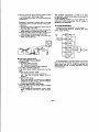
This repair is dilficult unl€ss you have 8ome
Itrput\ronag€
.
knowledge on transistor OwOFF function, NOT and
B
0
0
IANDI D IXANO
1
0
o
o
I
1
I
d
a
b
c tQat
o
0
o
o
1
I
I
.
Exsmplt
d
tNoFt
I
o
o
o
+
t
t6nsmit. D73 b dofsctive,
(See
12. Check pln 18. TXl,
l:
TS€50 does not trensmit sigrnls. O49 in the lF unlt
is defeqtive. (See pag€ 35.1
13. Ch€c*
14. Ch€s*
15. Chcck
16. Chcck
of lC1 1 in th€ digital unh.
ihe UL line in the digital unit,
the CSS lln€ ln rhe dbiral unlt.
the coll€ctor of O50 in the lF unit.
the bose of O5O.
17.D73 is dafecti\€.
l.
Press the SEND button and chec* whether 8T ie
applied to the TXB of the lF b@rd2. Pfess the SEND button end check whelh€r the SS
line
outoutvohcoc
Outoutvohcoc
2. Check th€ SS line. lO52 basel
3. ls the O52 cdlector 8/?
4 ls the CTXB HIGH? (TRX On a
5. ls RLB HIGHT (BKIN pin 3l
6. ls NSS HIGH? {BKIN pin 8}
7. Check lCl 1 pin 10.
8. Check lctl ptn 12,
9. Check Q+9 pin 2.
lo. ch€ct( o49 pin 3,
1l, Ched Qa9 fin 4. (Lowl
o
o
Exemple 2:
TS.[50 does not
page 3e.l
1. ls the TXB presentT {lF unit TRX pin 5)
NAND circuits.
A
+t
OUT
lalb to 0V.
Ch6ck rhe rnhrcomputer Don:i of th6 lF unit and
d'rgital unit.
3. Check the CTXB on the TRX board in the lF unit.
Reception: 0V: Transmission: 5V
4. Check pin 2. FLB, on th€ BKIN board.
Does it go HIGH?
5. ls any voltege applied to the Dl terminal on rhe BKIN
boandT
]s 8V pre3onr?
0 Check pin 10, NSS, on the BKIN
boarcl.
ls any voltage presentT
GND
T-....>a.*ai"Thlr rwfrch lr OFF Thle rif,irch ir Ol{
-3a -
a
i4FT
r__J
EH
lr:
itruJ
IIEf,
.t--:--l
TSGII
lF
-3t -
unit
I
Tnx(x50 -:]580-Ott 23
I
l-;tI'ua-iE-o,Fl',s.-l
ncm
ffiro
T..ff
+f
tcr
;ot
Y*l
*l
tfrB;H
lu
I
rffi-r
Irra.r.rtd
{
tr
dg
a,.l'
lc
ze,.
to.r"iJ
7. lf the curront is rbout 3A: Check th€ DnV OUT
Ponv* lc Odput
(Thc ON-AIR lndicator Llghel
2. No TronenrLsion
terrninal on the BF boerd with en oscilloscope.
E. lt is oK it it is about 2vp-p when the GAR-VR ls ser to
l.
Enter FM or C}r/ mods. CAR-VR: MIN
ln CW mode. eer BK-SW to SEMI or FULL.
2. SENDbrnon: ON
3. Slowly increase the CAR-VR frorn zero.
4. Observ€ the amm€ter on th6 por r€r supdy.
MAx.
9. ll tho drive'rs low, a previous cicuit is defective.
10. ls tho LG1 level oorr€ctl
lf the current exceeds lOA. thi linal unit
is
consid€red to be uorking.
5. Use the SWR meter to measure ths $/VR.
lf itgoes off*cale. a wlre botwesn the final unitand
tho ant€nna is broken.
6. S€t the CAB-VR to sbout 8100, and chec* the level
with an oscilloscope.
Measure ANT. LPF OUT, LFF lN, end FINAL OUT in
th6 order lbred The l€vel increages et some point,
Ch€ck it carefully,
I
3,Low Powcr
lf the power is low, turn the ALC adiusting var'nble
resistor {VBl.
CAF VR: MA(. POWER VR: MA,Y,
ALC adpsting VR: MA)(, Frequency: 14.2d)MHz
l80w or h'lgher can bo output. Reduce the cAR.vR
immediatoly
.fter confirmrtion.
(See page 41,
'Maximurn poruer is low.'l
lf the power is outpul, rhe final unit is OK.
following circult
connectors,
13
11. 13 the lF signal levsl conectT
12. Does the mixer circuit work corr€dly?
t3. ls fie LO-2 lewl ctrrectl
14. b t'te TIF sfnal lewl corrcct?
15. Doos the mixcr circuit 2 ops.ote conectv?
t6. ls 455kHz CAR ourp'.rt? .
A
susp€ctecl. Check rh€ LPF relay and
Or rhe linal unil or a/circuit before the driye is
dEfectiv€.
tor. dltlcrtur frnd
unh (Scc ncxt prgcl
Use an oscillosopo.
CAR VF:8:00
Do not increaaa thc vrtiDble rcsistor (VFt
cxcativary. Otherwiee, the f,nal tnnslstor msy fall
dw ro high-ftqwney utecffing.
1. See the le€l of the predriwr base of the final unit.
2. See the bvel of the pred.iv€r collector of the linel
unit.
ThE collector level ls abqut five times higher then
th6 b€se lowl.
3. See the lEvel of gach bss€ of the drive ransistor ol
the linal unit.
I
How to ohcdr whrllrr thc llnal uhh or r c#auh
bdorc tftr drtv. h rlof*tivo
1 Conn€ct ttie iig sholn bclow to rhe DRV tsrminsl on
the RF boad end mEasurs the @tput level wlth an
oscilloscope.
lf rhe lavel is abo/t A/pp. the circu'rts before the
drlr/e are OK.
2. lf the CAR VR is set
Ch.ck
!o MA)(, the ttrtue waveform's
disto(ed.
lf it is a clear slne wE\6, thc driv€ is insuffbient.
114
MHzl
-3?-
4, Soe ths level of each collector of the drive transistot
of Ure tinal unit.
The collectq level ls sbout foor tirnes higher than
th€ bolarel,
6, $€ tha bvel of each baee of the final transistor.
6. Seo the bvel of eecfi @ll€ctor of the final trtnsistor.
Thc conecnor b\rel 'rs abdrt ten tam€s high€r lhon rhe
b€se le\rel.
ls there 6ny sta€p in which the gain
b lowT
lf therB ls such a stage. ch€ck the bass bias of the
t,onsbtor wirh € DC-VM.
ls itebou 0.6V?
YES : The output bad nny be too h'tgh. Chec* the
ouiput circuit.
NO : The bias circuh or a trsnsislor in it is def€ctive.
f
Ghrcklog lor
lf at lcast 0,6V is applaed to the bEse partern. the bias
circuit is nortn€|. The transi6tor is dgf3ctive.
It at hast 0.6V is not appl[€d !o th6 base pattern. the
ransisbr B OK. Check the bi€3 circuit.
(ll a bhs adiustins variable resistor NB! is provtded,
turn
lf h csn be adiusted to 0.6V or high€r, the tias
circuir is OK.)
[.
r dctccfhn Urrrirtor
r. SwitdthepowerOFF.
2. Fernove the bese of the traneistotr. (For pushfull
3
Wp€. rerno\re both basss,)
Ponrer: ON. Mode: USB, SEND bunon: ON
FIHAL Ur{rT
lX.5-r/r?O-@'
TS-4t0findunh
-tE -
I ll r clrcult brlon {rc &lvc lt ddctlvo
4. ls the LG2 input ro th€ rnixer circuit?
Checktha lewl.
5. lg tfre TIF signel input to the mixer circuit?
SEND: ON
Ch€ck lh€ le\rsl.
6. Check the lqval
l4.ZXlMHz. Mode: Oi/, CASVR: M&\. BKIN: FULL
Connest a 6Gohm jb to DFIV OUT on rhe RF boatd,
t.
LGl
alt€r mixlng as well as the
frequency.
input to th€ mixer circuitT
Ch€ck the level2, ls dre lF signal ingut to the mixer circuit?
10, Ch€ck thc bias voltag€ qf the FET that g6neftttes
Checkttre lewl.
3, Check the level snd the frequency of the mixed
1
ls the
ALC.
1.
ch6ck the cAR hv€I.
signal,
Grnnot Adfurt PorYrr
lThc Domr crnoot bc rdlu$rd by th. ALC
rdlurtm.nt v.d.bil. rolAor lvRl.l
1. Chock ths ALC det€ct'on dirde in tho filter unit with
dcl@rw.
The refermce voltago and po*cr olths ALC sholtld
3. Does fhe dtao€ at rhs middle point of $e ALC
IVSF) variaUa r€si3tor (VR) change when it is
,0.
ln
t{nis aag'a.,
mo*ly tha
ALC lc
bc cdluztcd.
Fkuil squol dn refarcrw voltryla lf h ia incorrsct,
verlous problomc erioc (lw oxamph, tlrc ALC anqtul'
lo alwoys off-scale, thc mater pointar doce oot
move et tll, ot the powst ie too tow ot too highl.
a telrtar (phm rang€I.
2. Ch€ck the VSF line voltage with a DC-VM while
twning tr|o CAR VF. A3 th€ powe( increases, thq
VSF
lrolt{B
increeses.
rrrnedT
4.
ls tho
negEtlv€ volteoe
r-ff ert
l,rrlt
tll.HrSrartllc.trF
!.r{l!rSa.nElhf
_*-+-+J
lLglL--
7rC&r
applied
5. ls thc ALC vdtage corectT lf not. adiust it,
6. ls an approprbte voltnge apliecl to ths transbtor or
FETthrtg€oe(6teg ALC?
ttttlr
for the ALC
cofrectlyT
_J
6attat hrl
T9E50poworcofirol
_Ee _
-
Connect the ffi end powar rnetor Es shoryn below.
Setr 14.2G)MHa Moder USB. CAR VF: MAX.
P\A'RVR:MA( MIC: MIN
5.ALC Mctcr
Tha ALC e type ot fe€dbeck cirq/it. Tho nleter
's th6 te3dbacl tc\,a|,
poinlor indkFtos
lf yor adiust the power of the 18(M/ finat unh to 1 (XlW,
the ALC m€ter rsading corresponds to 8[}W.
lf pu adlust the poursr of the 12Ol'/ linal unit to 1 0OW.
the ALC met€r pointer rnwee less bscause'rts reetling
coresndsio
3., ALC rngFr
varlaue rrirtor (VRI
3. Adiusl ths ALC zono MAX.
varbblo resbtor lVRl
2OW.
It Mtiar : ALC
AG:
l$ffir'
MODE: USB
MICVR: MIN
RF
uct Fafi
Rclr
ANT
RF
vnlt
''trl
fiF
TP6
AG
F|Ull
tflc
AFV.M
hsfid
Flrd
DCV.M
+
A.$rst p.ioJ to
vollsoe Gvlatdr.
lnternal semHixed
o/
rmit\rBtl :lr/lAX
SIAY:
SEND
2lAG: thHalSmV
STEY: SEND
3l
Adiusl the meter to zcro. -+ lnternal semi-fixed
wrbble tosBtor{VRl
2. Adjust th€ mster start point- + Front panel MIC
1.
AS: ltHrrl0nv
SIBY:
fthrsr !o lha ALC
rngt.rql'fflghls
drh Mlr vQ
vn12
ACurt so ilrrt ALC
rnrlrr llghtg to
SEND
M'Y
?on€
-l--r!rtI
-ac-
f Crdon
Adiust the ALC to z€ro at poinr A. f it is inconect. the
ALC rn€ter doss not op€rate pr@€rly, so the ALC rnay
not be adjusted
ForW[6t
Thr yobea bacomsa raro lha nr3l't'[na.
Ylthon
tlr. wrl|bla .rdEtot
lvRl h lu?n.d clochf,lt
ilnL, th. polntr' b.ginr
.navlng,
- {o-
r
Refur to the 'Low Powe/ on page 37.
6.Thc Mcx FoYrrur ir Low
Connect the set diractly to the Dorver mgter from
OUT of the linEl unir.
lncreaee the CAR VR skrwly. lf th6 t00{ , model
outputs 170 to 180W. ir is OK. The TS-950 outputs
about 2001i/
I
Caudon
$is case, ALC end protection do not wo(k.
It rhc ouFut fpvver is too high. tho finat trensislor
fails. Decre€se th€ CAR VR to reduce ths powsr
ln
imncdetely aftor lcrifying $at
ouprjt,
$e
moximum power
c6n be
Pey enendon to lna cufi"/ot capscltr of the pvwr
swP,v.
It the @wl/reupply hes a red zonc of 2i2A aN the
maximum curnant of 264, thc power can be nlsed
to up to about |lOW end currcnt grotection is
actlvttcd,
ll you arc using such a powq suppty, you may
coasldar t
|'l ttc fincl unlt is OK fi th. Emmettr
Na
gops off-'€olo and thc itf,icsfptr charug8 ft!/m
cc
Topolrrnlg+
mtpacdnrarot
T9850
75-ta,lo
7.SUVR
3.
Mstcr
When th€ $A/R meter feils. lhe diode in rhe SWF
d€tgctiorl ciralit tails in mosr casos
Th6 imponant point fo,r troubbrhootirrg SWfi dctods
is the VSR terminal cf the fitter unh.
1. As the @w€r increases slowly, the VSR votiagp
incree€€e gredually.
2. The VSR roltage is edlusted to the minimum widr e
trimm€r and so on when th€ antenna t€rminal
rerrninated with 50 ohms.
iB
-6
lf rhe antcnna ts rminal
65 ohrns, not 50 oh.ng, tho
VSR voltage increasee lor en additional 5 ohms
when crmpared with th€ vohage when fte rerminel
€ 50 ohmo. This voltage is convertad to rhe SWR
meter indicetbn.
Yo.r cen locetc
volt€ge.
I
delective pan by checking the VSF
I
VSRvoltrgor{urtmmt
l. when the antenna re.minal is tenninSt€d with
50
ohrns, pourer ol about 25W'rs output.
2. AppV thc DC-VM prob€ to th€ VSR termin€l end s6t
the voluge to MIN by TCl.
I
Crudoo
Some rnanuals specw that the output po.ver should
be 1O /, but 25W shqlld be outpr,rt to pr€cisely adiust
the \ol0ag€ to MlN.
Do not put any changor betrreen rhe €ntenna gnd
dummy when adjusring rhe SWR NULL. Otherwisa
the minlmum i/ottBg€ point shitrs.
8.RF MGtor and Power Mctcr
The RF mstEr d€t€cta thg trensmifter wath a diodc,
converts h ?o a OC voltage change, amplifies it with €n
ope6donsl amplifler. and operetee the mster
Some recent rnodgls share thaVSF spnals.
I
Th. m.Or polot r do6 not movc
l1i9tE0 or $rbr.$t.nt moddrl
1. Receive about a 4clB signal from lhe SSG, and verily
that the $mgler porntor rnoves.
2. Enter the transmit mode, and ch€ck lhe VSF
voltego.
Do6E the VSF voltage rise when the power
incr€asgs slo,rvly?
Check the voltage of the nriable rcsistor {VR, used
to sdjust th€ po^r€r msiEr.
4. Ch€ck the voltag€ st lha power rneter inBrt port of
th€ mft:.€cornputef,
The m-rcrrcornputer port do€s not scc€pt signals il
tfie innrf wtuge excseds 5Vlf it ls higherrhan 51/, h is thc causs of this problsm.
(Th€ citcuir oontains e zgner diode for Bxcessive
3
rolurgo prevsfitiofl.t
I
Tho mrtrr ir ofi-roelo
Make a dteck in ths gsm€ way as ebove.
fha voltlg.
I! outgut.
! tt.n udog mcnr' li urd
l.
F any volt€ge present at th€ PVVM terminal Of ths
fiher unh?
M€tqr chulgG lwitch; POWER, MOOE: USB
MICVR: Ml,N, SEND: ON
2. Sstthe tGt€r to the ohm ange and apdy the probe
to the fry\,tl ulrminal.
lf rhe power meter pointer mo\r€s. the ci cuitt from
thc termin9l to the rnoter a(e nornrat, Reler tg "SMetcf
Do not Dut any clranger betwe€n the emenna and
dummy when adiusring rhe S1A/R NULL. Otherwise.
rhe minimum voltage point shitts.
-a2-
sect'xrn.
9.Break lN
The TS€50 and suboequent modets are modularir
Gt I t<Qrat
sd. Replecc.nodulcs.
rct
Feplac€ th€ nrodul€$ in the order of BK-S1A,, BK-IN. and
DELAY,
lafal
.
BK-SW
This board sets transrnission conditions. Signals
Gtn be tr€nsminod with a key when the C1A, is FULL.
th€ vox turns ON or OFF, transmbstom outsids tlle
b€nd i$ inhlblted, or the C:w'ts enterld.
DELAY
Scrs Oe delay time for VO( ON or SEMI BK-IN,
BK-IN
.
.
Controls the CTXB terminat on the TRX board
acoording to the oondrdsts of
fie
BK-SW aod D€LAY
boords.
10.
vox
The T9140 and subGeguent s€ts are modularipd.
Fi6r, replaco tha modulss.
.
vxs
Transmlsslon/l€csptton @mrd lin€ wh€n VOX'ls
ON. This line goes lor r in rhe lollowing case;
The mbrophone signal oflteflt rhe Vr(Z lptn g!, but thc
AF sbncl (bGs not ent€r thr AV lph A.
11. PROClhoccscorl
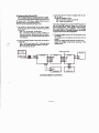
There are turo typ€s of procEssorg-
.AV
ANTI VOX
r
lin€. The receiver AF signal tinc ia
connest€d to this pin through th€ ANT| VOX VR. AE the
AFVR b tum€d, the AF signel bwl changcs.
.YE
ao
RF
tyD. lT8€0O, f$OaO, fS€SOl
Convsrts the transmined AF signal to tho lF sign€l
rnd amplifies lt.
The follodng block diagram shows thg TS-940
processor. Whon the processor is OFF, rhe lF sbnal
p€$cathrough D79. When tha pfoccssoris ON, the lF
sbnol preeos firough O40, lC4. O4il. and DaS.
VOX GAIN line. The AF signal from ths rnicrophooe
conn€at€d to this pin through &e VOX GA|N VB.
--a
Pr€d(trl.OFF ritch
o-#-+,frlcPR€ln L;f-o
Cqnpra-bo bral
,'
stt
,e
arilCAi{?
O37 fitfr
S".
artll
AT'P
T
Clp
&ilb
Alf2
Ai.P
Grln cqluol
2t
CranrE!6.rlt
oqanf clret
o.r.{t oo
-43-
llnlrEf
ATIP
FFC'C OUT
AilP
f AFtyDcoiolhf rett
lncraaso tho microphone amplifiBr gain.
lf the prooessor ls oft, O41 i3 otl. and th€ gein of lG4
dotcrmincd by Rl ard F3.
b
tf thB proc€sso? sl,vitch b ON, EV is apptie<i to rhe bose
of O41. the p€n between C and E ot O41 is shorted.
and tha gpin of rc4 is determined tsy Rl and R2 hrhk*t
are connedcd in perallcll. antl R3. ln eddition, the O42
ALC circuit sterts operdt-ton.
12. Trunrmlslon Tono Quellty
88A
r
L
lr
2. Adiust tfte transmigsion frequenoy charaqterlstics.
Poor
fiunlng[
The 2TONE trBquency is tlifferent from rnodet to
Check the linal bias.
Mode: USB, C.AR VF: MlN. MICVR: MlN.
SEND: ON
rnodel,
Thereforp, the adiustment p.ocedure dapends on
modols. Adiusr the trunsmission frequency
Chack the base voltage of the dfiver rnd porrv€t
traBistor in $e fin€l unit.
lf it is 0.61u or higher. t'le transistor bias is OK.
charactsristics
G
instn ct€d ln the rnanual.
Por^rlr
mdarot
A'{T
Tll8tll.rc
ss tPrn
GNDIME)
re mi.l
-4-
Mrc
M.wltofi
tbo|l!
grrll *tcl
t3. Dcfcstlw PLL
lf the rnodulatlon rcne is not stabl6. suspect th€
PLL. Refer to the 'PLL' section on page 59.
lf the TgfO r€ocpti)n BPF (RFl diode faits. modubtbn
cannot bc cr€cut€d proporv.
11. Powcr Fluctu.tlon
ArC voltego flucilurtlon
f
Oscilloacope: VOLT/DIV; 20mV, SWEEP/DIV: 5rnr,
AC input
Chec* the AC lioe.
I
Porru rupgly volhgr ffuctuetlon
Oscilloscap€: Same as above.
Check the pq,vsr suppli€s fiXB. -C, 8C. etc.l
produce ALC.
I Gtdrr hvolf,uctrrdon
f
Oscilloscope: VOLT/DIV: 0.5V
Check th€ ca(aer input l€l/el and bcal signal level
Do thcy fluctuate?
a Foor llnrl bord prnrnr coniact
The TS-930 and TS€40 linal boad-s have a poor
contect via hdes.
Soldor lhe oomponent and solder€ct sictss of ths
board
apln
I ?mr l.PF ortl(-ix
rolry corn
Gt
lf thc transrnission LPF relay is doiastive, ctange
thc trancmission band and chsck wheth€r tha
syfnpto'Yl still pe6i9t3.
Chock ths 3ign€l line
ol the band at whach the
symgtom existe.
Lightly ttp tho TX-RX change .etqr ce3€ with an
ediusring rod. ll the eyrnptom ie confirrned, the
r€lay Etay be faulty.
-46-
Poor
qrir q locrl.efirl conna!&r
$8t
cortac]
Check the MX FET input l€v€l wirh an oscilhscope.
15. Hlgh
ll
Nolct
16. Mobilc
norse oocurs during rnoduladon. perform the
dreck as tollo/vs:
lA/hile monhori4g wirh another reoeiver.
1. Grcarnd the m'rcrophone input terminal-
t
rnd Htndy Tranrcrfurn
Do narrrtunrhrl3nrlr
Do€s rhs ON.AIR inditetor qn t on the disglay
when pressirD the microphone PTT key?
.
Laeht
The transmission request signal entsrs the
rnicrooor.muter.
Th€ transmissbn r€quest sbnal is thEn converted to
digital detg and is sem to the shift regisrer lC and pLL
rc in the TX.RX unit.
These lCs docode $e ctrta €nd r€verse th€ voltag3 of
tho !€nsrnbsion/rFcaption swibhin0 terminal (TEl.
The T/e line is connsqt€d to the trEnsmission power
lgfl/receptirn power (8Rl switching circuit. So when
p-,ru
2. Ground or unground thc MIC AMP lN brminal.
rho T/B voltage ig reversed, the 8T/88 voltage is
r€wrsed.
't. Chrck
gT prsaant
?!
3. Grcurd or unground tha MIC Ai4P OUT terminal.
YES :
du.ing ronsmission?
ilo transmbsion po,ver is ourpu. Chec* the
dtive ixrtput or lrcO output. (see FItgE 37.1
l,lO ; Check the PLL module LD rerminal or thc shift
register T/B terminEl.
LO + OV when tho PLL ia locked; High whon it is
unlocked.
TIR
This sho!rs Wreth€r rho ndsa occurs when thc AF
signal is iasued or efter CAR conrorsix.
lf the noise occurs after CAR conwrsion: Thc PLL
probably ls defective.
I
lergr nobcfrom
hl
p€ge
nodolr
1. Bepbca the PLL VCO IFET and tflnsistoil
2. Replace the PLL lock voltago adlusting tritnmer,
3. Repleca the PLL vrdcap d'nde.
cepscltor.
in transmissi<rn moOe; High in rcceptbn
6l.l
The tEnsrnissiofr request cleta is ouFut lrorn the
microcompuler immod'rately after the PTT key is
4. Replace the PLL LPF transistor and srnoothlng
5, Rephce the PLL
-r0t,
mods.
2. lf the LD is abnormal. check th6 PLL circuh. {Sce
the descdption of the PLL circuit on paoe 59.1
3. lf thc T/R b abnormsl, check whcther dsta i8 inout ro
rhe data input pin of the shift regiaer (PLL lGl. lsee
pressod.
Modcl or scrbs narne;
Transmiesior{rocqti,on snrithing
€.
At bast 80% of the problerns may be solrr€d by
now.
It tho VCO as rnodularizod, replace the moduls, (lf the
problsm stlll parsasrs, soo p€go 25, 'Defecitue naoaivor
tooa.'l
-46-
saOnal
Terminal rume'
Tn#2Or cnd TM€l 1; Mbro@mDuter outpur pod 'iST
rM-221 : PLL lC'SWl "S/t/2'
TM-e,l ondTtvt-241; Shift register lC'Im'
TM-701 and Tllf,702; Voltaore suppty salect lC Tt'
1M:721 ard Tlvt .?81; PLL rnoduls "TR'
TM-741 artTM-742; Shift registor lC T/R'
TM-732; Shift register lC TX
T&751 and TR€51; 'ST line from the microcornputer
Tf
.
Doas not llght
The transmission request s'rgnsl (bss not enter the
microcomputef.
t. Bedace rhe mioophone.
Transmit : The microphone is defcctive.
tbag not trtnsrnh : The PTT line is defedive.
2. ls any votoge applied to the PTT line?
YES : lf the vohage becorms O\y' when th! PTT
turns ON, the microcomput€r is dct€ctlw,
I
line.
A wire betl/i/€on th€ rnodub OUT and the e ntcnna
NO ; The pull-up resistor ig delcctive.
The microcomput€r port is defealve.
tie
Check
I
shoft€d.
3. Chek tho rnodule voltage (during uansmissbnl.
.
ground line.
G.ution
The MIC conn€ctor has two ground lin€s. One is
ussd for the oudio signal ground line. such es
microphone ehield. ard dssignstsd as ME or MGND.
The orher is usEd for corrtrolllng the UP. DWN, and PTT
end is deslgnated as E or GND,
Thes€ two ground lines are not connect€d at the
MIC side in ord€r tg prevent transmrss'ton rrctse.
They are grouncl€d et different locat'lons €n rhe msin
unlt !ide. (Th€ resistanceg ol th€ turo lines. wlrlcl| E 9
measurod with c t6ster. tre zcro.l
INPUT
The rottago is diflerent from .y€del to model. Refer
bthe SerubB Manual.
o Jlt.APCIDB!
r
S/ (5\R during transmlssion. lt drls pin is used for
APC, roter to the Service Manual.
VCC
Power
.
sryfly roltago 's
applied to the
OUTPT'T
(lt depsnds on models.l
When checklng rha ground, consid.r tho two
ground lincs sufficbntly.
OUTPI'T
LnC O'!l O
k gterldd
IT.RX Url'T
ooNlaor
alrt"??!t
t/EC CillD ir
lo
tln
T!ll3 unt.
uNlT
grtunrtrd
ln ttra
lx.nr( ul{17
acnrol unll.
D(B VCC OUTPUT
The c2<tomrl MIC GND ot the handy trontcetv€r ls
supplled fton the ground ol the encrnal cqeaker.
Sioca tha exlcmal miaophone iodt does not hevc a
graun4 tht erd,€msl PTT atnnot be openatod iusa by
lnwttlng ths plug into the mlcrophone aonnactot
oaly-
The SP GND musa alweys bc connected to
dtc
FTT clrcuit.
-47-
This
Th. 1.AV (DCI Uas is apdied to this output terminal.
noise is minimizcd at thc tlesign stage I
fnrut
VCC
line is directly connected to the power cord.
Rernove tho porver cord belor€ sucking solder.
lOfleffilse. the fuse will blow.l
The connection locations depond on models.
{MGND is grounded at a point whcre the trammisJon
GON'BC UT{T
b
broken.
The capacitor for high-frequency sneaking
as
tnmmbcbo pow* b lnlrllicbnf
l0Wmodel:2.5A
6Wmodcl:1A
lf the vottage do€E nol ohangs. check the ground
proventbn
Thc
1. Conn€st a pour€r suogly wilh an ammeter to the
trenscgfver gnd gter( transmi$9ioo,
2. Obsarve the amr,noter on the power supdy. lf lhe
ammetcr indbates the tollo$ring valu€. the povvat
rnodule's Ol(.
SO\fi/ rnodel :6 A
2514, model :4 A
4 Ses the wavgform at driv€ OUT. lUse
b
an
oecilloscope lor up
144MHz. aM use 8n RF VrVM or spectrum analyzer br 490MHz or higher.)
lf the drive lewl is OK, the npdula is defectiw.
ll the drive levcl is NG, chect the powei supply
voltoge et the drivs stlgc.
5. Chsckthe lewl of ttp driw input tsrminsl.
lf the lewl b sufficiont the driw circuh is rlefectirre.
ll th€ l€vel 'ts low. check theVCO.
I
ll tho drhrr
th. modulc
mrdorar b not rqr rt
ft. lnpf ol
.
Forribleccueec
(be3 not tum Oltl durir€ tanwniesirn. ffhe
grwnd pin of the lC is not grounded I
1. 0.313
See folbwing figure. APC ope(etbn. Thie ligrure
shows thst th€ drivc qrtput do3g nd gntcrthc rnodule
unbss antenn€ diode D4 tums ON.
Since the anode ol D4 ls connoclod to the +B line. it
rec€iv€s th€ porcr sup$ voltage. The cathode of dle
diode is connected to tho output terminal of the
op€ratlonel emplifier. To turn D4 ON. th€ cathode
wltage of D4 must be no fewer then 1.2V bwer th.n
the +B voltag€ duo to the output terminal of the
operadonal amplilier.
It the r,oltsg6 does not ctocrease. onsicler why,
2. Rglil or R3O{ is broksn.
3. O3l5 or 0316 docs
ransmbsion,
not turn ON duting
4. The porror swply volrge'ls notappli€d to the lC.
5. G|11 hasfailedThere are so rnany posshle Gauses like these.
The TH-25G {261 end subsequent handy t raneceirors
have similar circuit configurations. lModsls wirh
oconornicalbw pqpd
It th€ power is not output aftor the final module is
r€placed, check the obot/e i!€ms.
TF78 AFGahcuh
-
aa-
-
.
r &lilrbn lluncbo3
-
l.
qrcss
Fi.st. repbcc thc CTCSIi unit
Verity thlt thr unit ic not 6lccthr€.
Ir th. tonc frcgrrcncy corrcctT
2. The SOL doee not opcn durirrg raclptbn.
Doe. th. AF signsl €iler th€ RD terminrl?
CTC. CTD. lnd CTS lines rrc
Check whethor
fu
lhortad.
b
DTSS
th.r fie DTss ods
I . vo,ify
each lins conncct.d
m-tcrooorngutcr pott?
la 5C gesant?
to thc
3. Iho SOL d thc orhcr trenEc€iwr @ not opdr.
Check the rone ficqrcncy md moduhlbn with
lin€ar dqt€ctor. (88.5H& about 0,4 to 0.8k1.ts1
l.t'lolltts
51'"'u'"t
Trrnrmi$lon
@.recr.
2. The Sc[- does not opln durine ruc.ption.
Do.6 O6 AF slsnd enttl dr€ input 9in ol the DTMF
dccoder lCl
Doas the DTMF ttecodcroccihlor opeirtc?
b thc apprcprbt€ wltrgp apps€d rc th€ lC?
The
3. Chrractcn arc incolrcct fiFl-z8. TH-7E1.
DTlrilF
.pproprhta
i8
elrodcr
lC
+
b drficctire.
.
raerilt
ra{,trul{r
m#'.'. //
TONETAET
crrs8oil
t.a-slllt
9TAE €od.
DTSS 00{
l8
..t,\t'
-
SoLorE'l
-e-
Tnarmbrloo
30Lo?:rir
DIGITAL C'RCU'T
1.
I
Dirplay Error
FUrt chccl actollows
1. Reset
2. Turn up the AF VR and chsck whether noise occurs.
3. Connect the SSG to the antonna and check whether
signals are receivgd. (SSGOUT: '14,001MHz. 60dBX)
I I ignelr
arc rocolvcd
1. The rec€ption circuit and PLL circuit ar€ wwking.
2. The microoornputer PLL data 's @nect.
3. There is a defective pan betwaen th€ display darE
output circuit and tho display circuir In rhe digital
(controll circuit.
I
.
K.y polnls
Models with a dlsplay tubc
Turn the power ON and OFF sevsral timgs.
lf any segment of the displav tube lighrs, the display
tube and DC-DC converter are functioning.
There is
I
dafective part betwoen lhe micro-
computer and the displav drive circuit.
.
Models wlrh an LCD
Replace the LCD assembly. You can see whether
the LCD assembly or the digital circuit is defective,
lf the transceiver does not havg en LCD:
Check the voltage and wavefqrn ol the connectorE
between the LCD and dbital board,
5V, 8ty' (DC-VM), data line bscilloscope)
AppV the oscilloscope probe to the dsts line and
turn the 6nctder. lf the dat€ waveform changes, the
.
digital circuit is considered to bs functioning
properly.
.
'l
f
No dbpby, no recaFtion, no nolse
f
ilo dlcpley, but rccaptlon lr nomal
I
Abnormrl dbphy
t
Abnomrl diQby
The microcom$ltBr does not work at all. There is a
basic problem in the microcomputer op€ration. (For
example. Vcc is not supplied to the mcro@mputer or
lC; No c-locks are genentd; The microcomputer is not
resst; The data line has a break.l
The microoomputer tunctions properry- The display
is &feclive. (The display tube ls defective I
3. ls a voltage applied to the RESET pin
RAM,
of
I
:Eramplc},
+q:
but rccrptlon lc normal
{t7g - -
The microcomputer functions properly. The
microcomputer dbphy output data is wrong. The lr0
or displaydrive lC is dafective. (The microcomputer. l/
O, RA n, or ROM is malfunaioning.|
I
ly'O.
I
Abnormrldhptay (
..
l, no rcccption
malfurctioning.l
. ls the microcompderclock o\rtput?
and ROM?
I EBgggS'.9
no reccpttron, no nolta
The micrcornputer does not work at all. There is a
basic proUem in the microoomputer operation. (For
example. Vcc is not supptied to the microcornputer or
lC: No clocks are generatecl: The microcomputg? is not
reset; The daE line has a breek.)
The rnicrocomputsr lunctions properly. Unlock
display. ffhe microcompute/, t/O. or PLL circuh is
to Chcck The Microoomputcr
2- ls a vohage applied to the microcomputer,
The microcornput€r can be checked in thls way.
You should verify how the microcomputer runs and
where the pogram stops to isolate a fault.
I
Modele wirh diodes (LEGI
ls a voltage present cotrrmon Et lhc LED?
ls a \roltege appliad to the drive E and trans'lstor?
2. How
5, Observe th6 date and address lines with the
oscilloscope.
6. Check the lNT, WF, and FE with the oscilkrscope.
the
microcomputer? -+ 5 V lLorr for sorne mod€ls)
Turn the ps,yer OFF and check the waveiorm with
an oscilloscope,
4. Observe the ROM CS enO CS2 pins wirh the
oscilloscope. lPulses sre output from the pins.)
-50-
DirphV OK thc lrcqucnsy contlnucr lncrrering
ordrcnalng
The microcomput€r functions properly, The
micropfione UP or DOWN key is k€pt pressed. (The
microcomputst or llo circuit is shorted. (MU, MD))
I
IrVrrrcnotecccptcd
The microcomputer functions prop€riy. The key
input [O is defectirre. (The mbrocornputer or l/O is
malfunctionlng.l
3. ls any t oltage applied to th€ tilam€rtt of rhe dbplay
3.
Nothing ir Dlcpleyed
l.
Turn the power ON and OFF several times.
tube?
Does the display light even once?
shorted? (lt th€ about 5V zener diode fails.
ls th€ zener daoda connected lo th€ filament
. YES
SHEBAE
The DC-DC conveiler and the display tube are
fundaoning prwerly.
The display drivcr circuir. disploy data circuit, or
dimmer contolcircuh is defective.
.NO
check the input and o$put volfrtgss of the Dc-Dc
converter.
r There is no input vohage
Check the pow€r supply circuit of the DC-DC
conwlrtgr.
is disptayed.)
Check the vohage at each terminal of the display
tube. Negative rcltagresl
lf the same voltage b applied to the terminals, the
drirc lC is not working.
Check the drive lC input with sn oscilbscope.
Tu.n ths encodsr end ctpck the dst8 line.
lf eny data enter the data line, replace the drive lC.
4. ll no data entd the line:
Check lhe date lina with a
lesler.
iFrom the
micro@mputer output to the driver lC inpul
. There is an input voltage
Has the oscillating transistor of the OC-DC conveftar
failed?
Rsmove the transistor from the boerd and meaSure
its resistanco with fhe ohm range of fie tester.
2. ls the oscilleting transistor functionirg?
Chock the transistor collec'tor with an oscillmope.
.NO
Replace the tra nsistor.
Ch€ck the output diode bdctg€. Renrcve the four
diodes lrom the boarc, and m€asute each of thEm.
The DCDC converters of ths TS-140 and TS€80 are
nrcdularizsd. lf the DC-DC corilrerter is suspected.
replace h.
r
tcD
Neur models use LCD assemblies. Replece the LCD
assemUy
lf th€ model does not have an LGD assembV. check
the data [ne with an oscilloscope.
Check pints A and B with an oscilbscope. OK if a
ct'Eital signal b outprjt rr\rfian turning the encoder.
lf data arrives at tha LCD driver input and 5C and 8C
src input to the board, the driver lC may be defective.
The LCD assembly is regisbred as one unit. Rephce
th€ €ntire LCD assen{cly-
./
r'
\
-5t -
I
Car rrnrccivor
For some car t.ans@ivers, the
fla
cable of the LCO
assembly data line is soldered. Check for defecttus
soldering or shorting. ffF-751, TR€sr, etc.)
soms reflow{ype connectors w€re not soldersd
securely, and solder was separated due to shocks,
(TM-702. etc.l
I
'
Notas for checklng fhe LED
There are two methods ol lighting the LED.
Turn rhe LED ON and OFF bycontrolling the anode
voltage. No rroltage is applied to either end of the LED
when it is OFF-
p
vcc
I
t,
lf th€ display is abnornrl. the zebra rnay b€ insulled
inconectly. Disassembla the dbplay unh. clean the
zebra and terminals. and reassemble them.
(Especially, TH-25 ano TH€6 ser'es)
Turn the LED ON and OFF by grounding the
cathode. Vcc is spplied to both ends of the LED when
ir is oFF.
LCD
a.The Dhplay b Dark
I
Elgclrobc
Eoerd
Type ataehed by heat press (TH-77. TR-501: Both
ends of th€ contact ar€a tend to have poor contact. lf
tho contact becornes For. the dispbv thet should b€
invisible becomeg visible from some angles. (This
oocur lreqlendy in the inital bt of rhe lH-77.1
I
Flst caue
Contlct trea
f
/
-do-*#tl
Handytnnsccbcr
f, rhc dlcpbv rubc 1r uscd
ls the dinrrer circuit kept ON?
ls the heater voltagg lo^r7
Tha dlsday tube may be defective. (lf the vacuum is
low. the display darksns.)
lf the power suppty rroltagE of the DC-DC @nverter
is low. the displsy darkens.
lf lhe (rutput vottage of the DC-DC converter is low,
the dBplay elso da rkens.
lf rn LCD lr uccd
Tha back light is dark. (The DCOC convener is
detective. The fluorescent larnp of tho backlight is
defectiw. The porerguppVvologeis lor, 8C,5C)
An abnormal rottaga is applied to the LCD dtive lC.
The drive lC is defectivE.
ls the dimmercircuit kept ON?
Mod.bwlrh dlodor
ll"EDsl
The Gcent models do not uso any diodes (LEDsl.
(The rrodcls betore th6 TM-211 used thgrn.l
Whcn thc current flows from the anode to rhe cathode
sf rhe LED, it lighrs. check wherh€r the voltage is
I
applled to the anode,
The cathode voltege should be negative if th€ LED
ligrhts dynamically. Check it with an oscilloscope.
-
ll an LED b uc.'d
An abnormal vottagp is applied to the drive lC.
Thc drivo lC b defeoive.
The dlode is clefective. (Brightness is uneven.l
The po^r€rsupdyrcltage is low.
For any dirylav type, chedc as follows:
1. Check the powcr supply. (K, 5C, hcater AC linel
2. Checktl|€ trsplay unitvoltage.
3. Checkthe dhar circuit opdrationg.
52-
5.
I
Mcanlnglccr Dbphy or Display Error
Check whether tha transceiver can receive signals.
Reset rhe microcomputer. -r lt reverts to th6 initial
status.
HF: 14.@0MHz. USB
VHF : 144.000MH2. CW (l45.O00MHz. FM)
UHF : 430.000MHa CW (X tl40.O00MHz)
To receivs these signals, set the SSG freguenc"y as
follows;
HF; 14.0OlMHz.4OrtBp
VHF : 144.000MH2,40d8p
(145.@0MHz, 4OdBlr" MOO ONI
UHF :4!0.000MH2, 40dBp
(K 440.000MHa 40dB* MOD ONI
I
?gwet
is
socket is used to instell the ROM,
rernove the gocket fom the boanl and solder the
ROM directly to the board.
Replace the midocomputer. FAM, and FOM lC
in this order.
6.KryrErc NotAccopted
ls the F. LOCK switch ON? -+ Turn the Bncod€r.
Beset the transceiver.
ll tlrr trarcclvo' b not
ltc.t
1. Unplug the power cable with the po^rer swirch ON.
(Remove the batt6ry.)
2. Hold dovvn the reset key. and plug in thc power
cable. (Reinstall rhe battery.)
3. Resel lhe ransceivsr.
4. Check ths microcompuler or
l0
lf it is not
rnechan'rcslly locked.
it is electrically
locked.
I
TrouUrghooting
The TS€50 keyboard unit
on th€ next psge.
as
prorided as an example
lf the transcgivgr is not recet
Unplug th€ power cable with the
(Bemove fie battery.t
po|er switch ON.
4. Chsck th€ mhreonputer or l0 lCs.
5. lf fiets is a soare boad. use it to leplace the board.
Other boar& rnay be dofective.
ll a ROM
I
3.
3. Fe$t the transceiver.
ll rlgnds.re not rrcrlvod
The microcomputer does not work,
Reset the transceiver. -+ Refer to the
not turned ON 'section on page 8.
The key conesponding to the indicator rnay be kept
pressed mschanically or electncally. Press it again.
2. Hold down the reset key. and plug in the power
caHe. {Reinsralt rhs battery.)
The display deta line is defective.
The display drive lC is defoctivo.
The displey is defectivc.
I
than USB)
l.
are rcoohnd
dee b normal.
lf tho lilnaccilrcr 13 raaat
ls any special function indicator shown on the
display? lExample: RlT, XlT. MHz. e mode oth6r
2. lf such an indicator is displayed:
.
trth. dgnelr
PLL
1.
lCs.
When the Atvl/FM key is preesed. K3 and 52 lines are
connected $rough D3.
.
Kty chccklng procedura I (Tssterl
l.
ffurn the powor swhch on the set OFF.)
Connea the tester to K3 end 52. Press the AM key,
(Ohm xl range)
Does the ohmmeter operate?
l{ not. change th€ polsrity of the tester and nuke a
check again. The ohmmeter should operate this
time. H not the dirde or swnch Ls defective.
2. lf the ohmnEter op€rates an both css€s, rsmove thg
flat cable frorrr the digitel unh and rnske e check
agBin. It the ohmrneter attlop€rstes in both cases,
th€ kEybogfd boad is defective,
3. lf the s€t bocomas normal (1hc ohmmetel opentes
only with one polarity) by remwing the flat cable
fthe ohmrfloter pointer mons only oncel, the drgital
boad is defectiw. ls any l0 lC lead shofted?
Check all
$e other
keys in this way.
Example: lf the MHz key is helcl doarn: K4 and S4
lf rh6r€ is a spare board, use it to replace the board
Other b@rds may be defective.
.
-53 -
are connecled through D5.
--
.
'1
Key checking procedur€ 2 {Oscllloscope)
Suppose that E key is electrically kept pressed.
Observe drs waveforms of S0 to 55 lines and K0 to
K5 lin€s with an oscillosoopg.
The waveform of one llne ot th€ S group differs lrom
the wav€forms of the otlrer lines, and the waveform
. Turn the set ON, and observe th€ waveforms ol the
groups of S0 to S5 linss and K0 to K5 lines.
2. The waveforms ol SO to 55 lines of the S group
must bc thc some when the key switch is OFF.
3. The waveforms of K0 to K5 lines of the K group
rnust b€ the sama when the key switch is OFF.
of one line of the K group differs lrom
These are normal stat6s.
Examplc: Whan the VOICE switch is pressed, S5
data passes throuqh DG and goes to K3. The microcornputer reads it and recognizes tho data from S5
to l(! €s voice.
I
FiE€-l
t...dt
ILS! r.}rt I
I rlAEI
I
r--t
I
I
I
I
t=
I
I
I
I
tr+f
I
I
I
I
I
I
at a
I
I
KEVN'ANDUMT
(:o::,____-_
nrl
IAM KEY PUSI{I
T$8!n kot mrtrk circult
-
the
waveforms o{ the other lines,
Example: lf the waveform of Sl and l€ is abnormal.
the TX-A switch is being kept pressed.
t4-
{lt
7.How to Flnd Mioslng
lThroughout holce in a borrd, brolcn pattcrne,
cepechors or coib Gonn ctad tothc drtr finocl
Analog test€r : xl0 or xl(X) ohm range
Turn the set OFF.
Measure the resistance of the data and address
lf the resistance of a line diff€rs from the others. that
line is defective. The address lines must have similar
resistan€.
Example: A0 to Al5
A0 to A7 (The resistanc€s are alrrpst the sarne.)
1
Resisance diffors slightV
lines in both forward and backwerd directions.
The data lines must have almost the sarne resistarrce.
J
A8 to A15 ffhe res-stances are almost the s€m€.l
You can find defectiw linEs in this way. Then check
the causo of the drflerent r€sistonces,
D1
D2
D3
cPu
AO
AI
A2
I
htr a lowcr rccbilenco then tho othar
Remove lC leads. resistors, and capacitors
@nnected to the line one at a tirne. When the line
resistencs becomes the same as that of th6 other
Onc llnc
lines. the cornponent just rarnovad is defectirra.
I
Onc llnr har a hilhcr rccbil.nc. th.n th. oth.rl
A panem is broken or a compongnt has a p@r
c0ntact,
-55-
I
Conccp'turl dnwing
d
thc dlgitel clrcuh
The resislarrcE between DO and GND is determined
by the sum of the resasGncos ol the CPU. ROM, RAM,
and l/O ports, The resistances b€tween Dl to D7 and
GND are determin€d in the same way.
li the llne has a break ar poinl A, the res'lstance of
the l/o port is not 8dded, so ths loral resistancs of the
line b dilferent from $st of lhe othsr lines. You can
find a defecliw line in th's wey.
The data lines are mosrly pulled up wfth resistors.
Check the leads of the complex resistor with a tester.
llt is difficult to check the leads of the flar package lC I
Extmplo'
Common B is applied to pin I of the complex
regigtor. Pins 2 to 9 are connected lo th€ microcornputer data linas. Measure the resisrcnces with
respoct to ths ground.
Apply one test€r probe to pin 2. and measurg the
resistance of pin 3, pin 4, pin 5, ..-. pin 9,
Apply onB tester probe to pan 3. and rYl€asur€ the
resistarne of pin 4. pin 5, pin 6, ..., pin 9.
Apply ona test6r probs to pin 4, and megsure ths
re.sistance of pin 5. pin 6, pin 7, .... pin g.
Exrtttlry/c
.1.
Measure the data line resistances in this way.
ol tttc bed wcvdomtg
DATA
LINE
Assume thet each date lina runs from one adge to
the other of the dlgltel board, Therefore, Dl may
become adlecenl to D7 In the pattern- Dl and D7
nay be shofted, thoctgh it rarely occunl.
The above procadure checke for this problem.
8.
Chccking UYavcforms UUith thc Pows ON
Waveforms can bE checked whh the power ON.
though it depends on models. lt is €dvised to comparo
the wavetorms with those of anoth€r s€t it av€ilable.
Oscilloscope; DIV 5V or 10V, Sweep Trigger point
1. Remove the ROM.
2. While monitoring the microcomputer data line. turn
the porv€r ON.
lf no waveforfir aggears on the oscilloscop€, turn tho
.9ornc dcte hhrc hllf
lho ours{ lrYll of tha
normll drt!.
. No ovorchooling
'The waveformr are
rounded.
pot/ver OFF ancl ON agrain.
When the power is turned ON and OFF several
tim6s, a waveform is displ8yed.
3. Obsarve the wavetorm height. rising edge. and
overshooting
d
the data and address lines.
4. ll torminals
ar3 Bhorted by mistake during the check,
the wsvefonn disappears.
Turn the gotnrsr OFF and ON again rspe€t€dly untila
wavsform agpears again.
5. Locate the defective line in this way.
lf an lC laad is lifted during the
eheck
by this
method, ?he waveform disagpesrs. The micro-
com putar sto p s ope rat i ng.
This mcthod ls useful if the reslslance chec|fatlsto
lind thc ceu3€ of tfie problem.
- s6-
9.
t
t
Mobile and Handy Tranccclvcrc
lXgital clreult
The digital circuit is comprised of
I
single-chip
mrcrocornputer.
'l
5. Reset the tonsceiver.
rl
6, Check the data line that connects the main CPU and
li
7. Check ths soldered parts of the micr@omputer.
Before soldedng th*n again, tle gure to unplug rhe
poi/er cord of the s6t.
subCPU-
I
Before applying the soldering iron
DISPLAY,
FI,I- DATA
Ths contents of the intemal ROM differ from model
to rnodel. Pary spccial attention to thas when replac-iltg
the microcornputer,
Example:
TM441
Howtochcck
1. ls the power supply \oltago apdied to each lC?
2, Does the rnicrocomputor outDut clocks? (Also
check the sub€PU.l
3, ls the r€set voltage present?
4. A,re the rnsin CPU and sutrCPU grounded with a
bwresistance resistor (about 10 ohmsl?
75116GF-Z2g€BE
TM-702 7s110GF{g-3BE
Thase models contain microcomputers of the same
type. but the three digis in rhe middle of lh€
differ, so they are not compatible wrth eacfi other.
des
tip
Check the voltagE
of thg conneclor and the
waveforrn of ths data line.
When it is checked by orning the encoder, AF VR,
or SQL VR, digital data definitev 'rs orrtgut from Sl
and SO.
The recent multi-functional handy tr€nsc€ivers and
car transceirrers with detachable panels have a sub
' CPU in addition to lho
rn6in CPU, which communicate
with eacfi oth€r to transfer dao.
vcr
PLTDATA
RESET
CLtrT
BACXUP
Cld&flr
Mdrrrli
PocrrON
-57-
to
microcorrputer leads, apply it to the ground once fto
set the potentaal of the iron tip equal to that of the
se0.
L lf an LED stalrs lit:
Check the waveforms of the key outpul end key
retum telminsls vyith an oscilloecope.
9. lf tho cartransceivsr has a detachable panel, replace
the p6nel ass€ntly.
-lcdctcoolJ
Fdor.F. Sft
PLL CNCUIT
5. The DC voltage from P, Dout enters the lot^Fpass
I. PtL
The Pl-L circuit generates fie frequenciEs required
lor transmission and reception whh the transceiver.
I
Oporaion
1. The reference oscillator produces
the reference
frequenoy and sends it to the reference oscillator
INPUT of tha phase comparator tP. D.).
2.The VCO generates free-run frequencies. {lt does
so even if it is unhcked.)
3, Part of the VCO output go€s to the divider (UNl,
Dlvision datE from the microcomputer enters the
divider end the VCO signel is divided according to
th€ microcornputer data.
4. The phasE comparator lP. D.) cornpares the phas€s
of the ref erence
filter (LPFI, through which unwanted
ripple
compongnts are removed. The resuhing signal
enters the VCO,
6. Since th€ VCO uses a wdable capacitor diode. the
change in the DC raohage from the lor,v-pass filrer
indicates the chang€ in the capacitance of the
varicap diode, and it changes the VCO oscill€taon
treguency.
7. R€turn to 3.
8, lf the phases of the reference oscillator and l/N
VCO frequencies match lthe DC voltag€ is always
constant
oscillator and Frequency
clemultiplier outputs. The difference between the
phas€s of the two frequencies is converted to DC
voltage and output ro P. Dout. lf the phase
difference between the h,vo frequencies is zero.
proce€d to 8.
PUW
-59-
+
the VCO frequency is ahtara constant),
ths PLL is locked.
2. Unlock
Check all the bands by setring the BAND swirch UP
or DOWN.
I
Only particrrlar bend frcqucncics
thift
Check which frequencies shift.
.
l.
Tho VCO swirching frequency shlfts
Chsckthe VCO oscillation level of the last PLt bop.
Change
tha band to another ancl check the
oscillarion level. ls thore any band in which the
oscillation level is extremely low? {The output
should be 0.5 to 1Vp-p, though it depends on
models,)
o YES
The VCO ior that band is defective. Check the
oscillating transistor voltage and oscillation level.
The VCOs lor the other bands must stop oscillating.
V€rify thet they stop oscillating.
The VCO rrny not oscillate steedity if band deta is
wrong.
rNO
Does any signal enter the comperison lrequency
input pin of the PLL lC?
See pege 64 and check the comparison flequency
input of the PLL lC.
I
.
A ocrtaln rrngc of hcquendcc la unloc*cd
llhc rrngc b not dc{lrilc a ne rll thr brndc unloclcdl
See the PLL block diagram on page 64.
Example
The D7 voltage is zero. lLock: 5V; Unlock: OVl
lf lC9 is unlocked, do nqt check only this kcop.
Tho comparison frequency of the loop is a combinetion
of thelrequency produced by O18, the lCl PLL output,
and the lC4 PLL ouQul.
lf the lC1 or lC4loop is unbcked, the lC9loop mayalso
be unlocked. f lhe lCg loop is unlocked. the lest loop is
also unbcked
To repair a PLL of a hlgh'freguency (Hfl transceiver
or all+node transceiver, it is a fundamental step to find
the highsst-level unlocked loop.
The highest-level PLL loop of the TS440 is the lC1
and lC4 PLL. The lest loop is the lCtT loop,
The lC18 loop is an independent loop. lf rhis loop is
unbcked, it does not atfecl the other loops.
I
l{ow to flnd unlodcd loopa
The PLL lGs has an unlock d€tect'En pins.
-60-
(Some lCs have
a
reverse logic.l
Check Ell the unlock dotection pins. (Use e oigital
voltmster or oscilloscope.l You can find unlocked
loops
.
an
this vmy.
lf all the loops are unlocked
. Chtrk $e oommon power lines (8C. 5C, and 15C).
2. Check whethar the reference oscilletor is working
and whether the reference frequency is supplied to
1
altthe PLL lcs.
3. While turning the encsder check whether digrtal
pulses are input to thB ddta line of the lC.
.
lf seyeral loope rre unlocked
lf two or mora loops are unlocked, find the highest-
level loop.
1. Check whether any signal is input tro the reference
trequency input pin and comparison fraquency input
pin of the PLL lc.
2. Check the power supply rcltages of the PLL lC. low@ss filter (LPH, and VCO.
3. Check the data line of the UNLOCK lC with an
oscilloscops.
4. Adiust the lock voltage as instrusted in the Service
Manual.
t rl.tt.
T$,aaO RFunh
Low
Locked: High, Unlocked:
tirtqt.rlr
b(lt
.
I lf onlockcd loops rro not drlactcd
dlehel
volhct.t
wlth thc
Check thcm with an oscilloscope (lC UL pin)
VOLT/DIV: ?V Sweep time/DlV: smv to 0.5mV
Gharqe fie SWEEP/DIV in rhls range. lf lhe incornect
waveform shown below appears, the circuit is
unlocked.)
al
b'
3.
Howto Gheck the
PLL Data Llncc
lll
1. Apply rhe oscilloscope proba to the dsta line of the
PLL lC and check whether a digital pulse comes
lrom the digital circuit.
lf a digital signal is present, the deta line is OK,
2. Check ell the cK. DA. tE. SCK, and SO data tines
3. lf no dsla arrive at a data line, c-heck it again wiih an
oscilbscope.
4. Turn the encoder. lf d6te b tound, the lin6 is OK.
5, lt not. change the rnde, lf data is detected st this
tim€. the line is OK.
6. lf no data is found, turn the power OFF and ON again
soversl times. lf data arrive at the line. it is OK.
lf a dlghal signal enters eEch PLL date line, the dam
lines are OK.
bl The VCO oscillation lrequency-s unsubls.
The lowfass filter clres not work properly.
lf
no data enter a tine, lhat lin€ is
defeaive.
The comprison frequencny level is insufficient.
The data output VO is defective or a wirs between
the l/o lc erd PLL lc is broken.
cl The PLL is malfunctions.
The VCO does not work 9op€rty.
tl.llow to chrc* the
PLL Data Llnes
P)
Turn the set OFF-
Set VOLT/DIV to 20mV or 1OmV end mske a ch€ck
Each PLL lC has a data line, a clock line, and an
agarn.
enade line.
rl
.
Examplc: lf lhero are four PLL lCs
DAO to DA3. CKO to CK3. end LEO to LE3 data lines
are connecred wirh the PLL
lcs.
{cK and DA lines may
be shared.l Check rhe r€sistance of these groups
lpositil/e anO negotiw poladties).
The lines of each group must have ahost the sarne
resistsnca. f tre resistancs of one line ditfers from the
others. tlet fine is defectiw.
Check the lines by referring to the digital circuit
section on page 55.
b) The VGO oscillat'ron freguency b fluctuates.
(fhe VCO ransistor makes a loud noise.)
The lowpass fiher uans'rstor makes a loud noise.
The smoothing capacitor diode is defective.
The variable capacitor diode is defective.
cl The waveform is influenced by other PLL loops.
Check the high{evd PLL loops.
-6t-
5.TIpt for Rcpair (For Repalrlng pLtsl
1. The tevels
of input pins 2 and S of the mixer
3. When the TS-7S. TS-81 1, and TM4xx are repaired,
a limited number of p€rts can be checked with an
oscilloso@e, See the measuremgnt seotion on
lC,
SN16913P, must be alrnost the same. lf there is a
large difference between fiins 2 and S (lwo VOLT/
DIV ranges or nrcre). one of the 2 lines is faulty.
4. Before acljusting the lock voltage, read rh€ SeMce
a PLL is unlockgd, does not necessarily
6. You can determlne which circuir iS defective by
chocking the PLL lock voltage.
page 96.
Manualcarefully.
lf the mode or frequency is set inc€rredly during
adjustmenL atl6ther probbm rr6y occur as a result.
5. How to check the VCO operarion
lf tha PLL is unlocked. the VCO keeps oscillating at
free,run frequencies.
connect the freqGnqt oounter to the vco output.
and tum the lock voltage adiustmcnt coil (trimmerl
whilg monitoring the fraqucncy.
lf the trgquonry changes, the VCO is functioning
WW
M@
2. Because
corr€ctv.
lf it is 0.611 -) oither the VCo is not functioning
properly; the reference frequency is not input
mean the PLL unit is dsfEctiw.
The TS€aO has Mro PLL circuirs in the CAF unit,
four PLL circuits in the PLL unit. and the last pLL
VCO in the RF unit. lt is therefore necos3ary to
check the CAR, PLL, and FtF units for repair.
The TS-950 has four PLL circuits in rhe CAR unit,
four PLL circuits in the PLL unit aod the tr^o pl_L
circuits in the AF unit.
The TS440 hes five PLL circuits in the pLL unit. the
last PLL VCO in the RF unir, and a 8.37SMHz
oscillato? circuit in lha lF unit.
Also check the controt ldigitat) unh that is comrnon
cone6ly; the qJrnparison frequency input is wrong;
or the porer supply line is defectirre.
It h is kept high + sith€r data are incorrect, or the
bw-pass filter or the PLL lC is delective
Use this inlormation as e guide lor repak. fThere are
sorne exceptions,)
7. The checkpoints of the T$440 PLL are shown in the
block diagnm. T$940, T9930. snd orher models
with multiple PLL loop basbaily sre checked in the
same w6y.
to all the npdels and power supply tines when
making a repair.
-G2
_
6. DDS lDlrest Digital Syntheslzer)
TS€50 and subsequent models use a DDS lC as
a
rler osci htor circ uit.
The DDS synthssizes sine waves with digital signals
and produces signals with little distortton and a high C/
car
I
N ratb at low cost cornpared with conventional PLL
oscillators. Since rhere is no PLL lockup time ftime
after the frequencl chang€s until the PLL loop ratums
to normal status). end it responds quickly, it
is
advantageous for CW full break-in and AMTOR.
'E
rlar
DDS lC : YM8581
f
l
bbct drgnm rnd dst lormrt
Chtd(proccduro
ls $e power supplyvoltage present at the power pin
of the DDS lC?
2. ls the referenc€ frequenqy input to the CLK pin of
the DDS lC?
3. Are dao input from the CPU to the data input pins of
the lC?
(YM6631 + pins 60 to 6; F71022 + pins 1.42 to
44, See PLL data line checking method I on page
61 for details of data checking.)
4. Replace thE DDS lC.
i!iSilili:irli!::!i
qam{a
tx
tFb
*.i
k-.-
tr
r--^--^
.; iiFitFatStIttEEiii!
-68 -
;
n
7.
T$440
PLL
O
Chcd(polnt3
: Check lh€ lsvelwith an ogcilloscope.
: Check the voltage with a digital voltmeter.
B: Base E: Emitter C: Collector
A
S:
Source Number:
Pin number
a
I
I
I
I
I
I
a
I
a
I
I
I
I
I
I
I
I
I
a
a
a
II
a
I
I
I
I
I
IL
-6f-
8.TS-440 Lr3t Loop Checkpoint
O : Check the levelwhh an ccilloscope.
A : Check the voltage whh a dighel vottm€ter.
B:
AF
Base
E;
Emitter Number:
Pin number
UN'f
PLL
I'I{IT
Aan ,,-r.
-<ttt
A
OUT
I
I
I
I
I
I
I
hqn
f tJf$l
-t5-
9.
Ouick Ghart of PIL lC lnput/Output Pinr
R: Refurence frequency input
U: UL deteaion
C: Comparison frequency input
O: DC OUT
G: Ground
V: Power supply
D: Data line
F.O.: Frequency out
G B
VOU
ls..fi,ts-.ao,
f6-''.t)
vi
c
t
voGuG
ooc
D6
fl'-ta0T9''o
fw4tn.fs.g,
7S-'{0
vo
ooo
DDOi
o
O
TSdr
Vi
UC
ucra$ntP
c
vo6
n9.ca0,
t:97rr.
voouc
f'-9:r0,ls.7ffi,tn-mr
TS-7 I L rS-Et t. lltt.2t t
19.64 1964
MCrSrsrP
uc
71t
iGOg
trt
C ODO
l*21,
f&tto
tlt€tQ t&eil
tFt20,
l
G
G
tn$L7#Or,lM-z1ro
DDO
6GtV C
U
slrllna
vci
o
uc
oDo
t
TkTW
c
rs.$osDr,
+27
ls-tg
!Gem.I5!.r2!l
oaoooo. aoo
lcfltAP
ouv icc
vuooo o
'rn-gru,nB.?ffi
r.ova*o
fHat fH4g
I$Elo
fH65
F€'9
KCI+o', XEH.6s3qa1g
'(Gt+tt,
KcH-t2,tn-r.r
-66-
01:VCO
02 ; Buffer emplifier
10. PLLI of Moblle and HandyTranecclvcnr
I Eramplr lTl+26l
G4 :AVR
G5 ; Amplifier
O24 : BX band-pass filter transistor
A single VCO oscillates transmission and reception
frequencies.
lCl
: PLL fC
lC3 : UL detBct'on lC
D2 : FM d'tode
Dl and D6 : Varbap diodes
D3 : Dioda for swiching the VCO frequency during
transmission
oz
cl
e3crtrt I rt
tt:tta rrltl
ot
rl6aoat
O
I
I
I
I
ol
ttcaoat
I
lscatrt ,rr
I
I
1
I
I
I
I
I
I
I
I
I
I
f|+28 TX-RX unlt
-87-
lB/21
AUXIL'ANY fiNCUITS
l.Nolsc Bbnker
I
Configurdlon
xottc
I
Fcprlr prooodurc
A noise g€nerator is required to repair the noise
blanker.
,
Connect the noise generator to the anlenna of the
set. Vsry ttre noise generstor output so that the Srneter of tha eet indicates about S-9. lf the set 'rs
normal. pulse noise is gliminated aod the 9meler lewl
decreases when the NB (NBl) switch lurns ON.
This is becausc ttre bias of ttre noice btanking gote
diode ie revsrsed if pulse noise occurs, and the signal
line breaks.
IlA{llllo
1. Connect the noise generatoc turn the NB switch
ON, and check whether the NB gate dide outputs a
pulse weveform wrth an oscilloscope. (NGll
2. Gerue the wawform of the base of the transisbr
that controls the NB gote. (O22-B)
3. Check wath an oscilloscoge whether the noise
detectbn output changes aeording to the noise.
.1.
to12al
ls thc AGC amplifier ln the NB circuit working
propedy? lo17l
5, ls the noiso arnplifier functioning correctly? (O1215)
-69-
GA?e
a
I
l.
Fcprlr proccdrrc (NBZI
Does the NB2 switching circuit oulput any pulses?
(NG2I
2. Does the wavgform shaping circuit output any
pulsesT llCE)
3. Does th6 NB2 noise detection circuit output any
pulses? (D&ll
forSl al^xrlNc
,ro.'a oattcT
oauil
I
I
GA?E
ort
oa:t
l=J-"*
auttairp
Notch Circ-git
2.
There are two typ€s of notch circuits: AF notch and
RF
I
ndch.
AF notch
*l
lr
I
I
I
I
I
vna
io(
r6ilTl
- to-
I
Troublcrhooting
The output terrninals of the optical. magnetrc, and
conl8ct-tlrpe gncod€rs are shown below.
3. Chacking procedure
tf the optical encod€r does not output the following
vwveform:
ThE waveform rectir'rcation circurt on the encoder
board may be defective.
vcc lsv, 8Vt
EN1
EN2
GNO
The encoder does not r/^rork
ls the following pulse output from the ENI and EN2
output torminals of the gncod€rwhen it is turned? lf
not the detectaon circuit may be dafective.
lf the 5V power is not supplied or the GND as not
effective. the oulse is not output.
2. Do the ENI and EN2 duty retbs differ much when
tuming the encoder?
Example (Optical)
ENI or EN2
5V
EFTI
4. Some initiel nrcdels of optical encoders may not
work if the encoder pulse phases do not match
SV
Et{2
exactly,
Examples: TS-770. TS-780: The STR lService
Tectnhal Rsport) has been issued. Fead it beiore
staning acljustment,
ln this case, the EN2 duty ratirc is wrong. Adiust h to
50:5O. The adjusting variable reeigtor (VRl usually is
in the encoder unit,
tl
the duty ratio of a magnctic or contrct-type
cncodcr is wrrrng, the encoder mutt be replacad,
-12-
T$770: No. D0-8G1O92, 1081, 1501
TS-780: Market quelity improvemenl r€quest No.
SC4lll lJuly27, 1983)
5. lf the ENI and EN2 waveforms are correct:
The waveform rectafacation circuit, gare lC, or
microcomputer in the control or dbital unit rnay be
de{ective.
w
T&aaO control
6. lf reception or transmission sometimes fuils when
the VFO encoder is turned:
The part of the vFo indicated by the arrow has poor
contact.
Polash
it cleanly.
since tha rotor is not gounded, the capaciranoe
changos and th€ VCO
s@s openting.
-?3 -
unlt
4. RF
Check whether the correct voltage is applied lo the
relay for both vpes of ettenusrors.
lf the r,oltage fror swhching the relay is normal, the relay
Attenuator
There ara two tlDes
models:
of attenuators according to
1. When thg anenuator
appli€d to the relay,
is turned ON, a voltege is
is defective or tha attenuator resistor has e broken
wire.
2, When the att€nuator is turned ON. the voltage to
the relay is cut off.
rRF
UNIT (X44-3130-OOt lAl41
r!
ar
ct
.r
Gtaa.t
02 \g+
o/trtattr
tr!
xto
rrtz
?,tt
T3-6oo RF unlt
tl
UrUT
tXrr4-tl2O.Ootl^lal
a
o i'i
lat I
u4
ol
llL.
JI
-.J
-t
s6
TS-t60 RF unlt
-71-
-
tE
a
o
Ei+ E:+ 3-
ta
a
a
o
5.
Fllter 9witchlng
The TS-450 8.83MHz filter switching is described
below.
1. When ths filtsr switch on the panel is pressed, a
signal is sent to the microcomputer.
2. The microcompuler transfers it to lC3 in the RF unit
lDA. CK LE) as dQitaldata.
3. lC3 decodes the data and controb the output pin
(OFF: High; ON: Lo,vl
E
trlr
I
o
?
a
EI
lc
-75-
f
6.Automadc Antcnne Tuncr (AT)
The automaric antenna tuner is installed betwggn
the set wilh e
.nl.nn
fha tutomatir: antcnnt trncr docr not work
1. check rhe cAB vR in the set.
(lt sufficient powar is not provlded, since the SWR
cannol be cletocteo th€ antenn€ lun€r will ,rot tune
or gtrop tunlng.!
2. Set th€t allows switching beh^reen the internal and
external antenna tuners,
Although the intemal antenna tuner is optional, tha
AT switch is set lo the internal antenna tuner.
output impedance end an
with an irrpedance of mora thsn 50 ohrns to
50 ohm
match their irpedances.
The impedance of the antenns matches es vie$/ed
from ttre set.
The inpedance of the sm also matches as viewed
Afthough the AT swatch is set to the externel
antennS tun€r. th€ gxtarnal 8nt€nna tuner is not
{rom the ant€nna.
The antenna tuner is an impedance converter es
oonnesled. ffs€80, T$450, AT-300)
shom aborre.
The euomaic antenna tun€r matches the antenna and
set autorngticel9. KENWOOD'g autornatic ant€nns
tuner guarenE€s ampedances of 20 to 150 ohrns.
oo
oo
oo
S,VFI botuYtcn lhc
and antcnnr tunal
$t
gWBl b.lrnon tho AToutput
lnd.nlrnna
-76-
I
Thc automctlc rntcnnt tuner docs not stoP
l$Gdorcc rotetlon tvpcl
lf the set of blades of the variable cepecitor rolate
360 degrees, check the rnotors,
Do both the X and R motora run?
lf either of them does not run el ell, check the motor
voltage.
ll
the voltage is correct, the motor is
defective. lf the volragp'rs incorrect, the rnotor drive lC
or a circuit befote il is defeaive. (Volrages applid to
th€ positiv€ and negatiro termanels of the molor: 0V:
(W or 14V: 14V.)
I
.
I
Presetting type
Res€t both the gpod and defecriv€ sets.
2. Set the AUTO/THROUGH switcn on the anTenna
tunBr to AUTO.
3. The variable capacitors will b€ set to the initial
positions. Check the positions of the sets of blades
of rhe var'Bble cepachors of the two sets. li they are
almost the same, thgy are OK.
4. Disconnect the power lines of the two antenna
tuner tnobrs.
5. Press rhe AT TUNE switches on bolh s€ts and
cornpare their vohages and waveforms.
Tror6lcrhootlng tfrc AT board
How to measure the rcltag€s and waveforms of lCs
in the antgnna tuner; lt is difticult to repair the AT board
if another ATboard is unawileble forcomparison.
Note : Connect a dummy to each of the two sets and
st8rt ant€nna-tuning. lf I migrnatch alert tone sounds.
turn the tuner OFF and ON again.
.
TyFe of which the vrriablc crpacitor ht! t cct of
blades thet rotot€ 360 degraes
1. Set the sets of bhdes ofthe variable capachon o{
th€ turc Entonna tungra to al.nost ttr same position
and unph8 the powsr lh€ of th€ rnotor.
2 Start the antenna iuner of tho gpod sst with the
open antenna and unplug ths power line to thG
motor at an eppropriate time.
3. Set the sst of bladss of the var'rable capacitor of the
detEcilve set to the same position as that of the
good set as follouo:
1) Disconnect the motor connector.
2
Apply about lov to the rnotor to activate it. Stop
it if the posation ot the s€t of bhdes of th.e \€dable
capacitorof the defective sgt rn€tches that of the
goodset.
(X, R)
4, Stsrt both of lhe anrenna tunsrs and oompare their
\roltages and waw'orms.
ATUNIT
-79-
This procedure is useful ln d€tecting incorrect
capacitarre of capacitors.
.
Exarnple IAT-5OI
The motor po^,er suppty has baen soldered.
1. Resat the tr'\,o sgts.
2. Desoklerthesol.
3. The vohages and rrraveforms can be checked while
tuning.
2. Rules for Pattg
The gcnoral llst
r
Llsts
The general list shows ths perts numbers in
ascending alphabeticalorder lA to Zl
A20-2634-15 (RZ-1t
Example: A12-345G03 ,
J
.
w02-1453-05
I
Tht lkt of PIC bocrdc
The list of PC boards shows the initial letters of
Examplc:
Thc lnhlaf lcftcrr of partc numbrrr ln thc
fnn lndlcatc a?oups of prrts
_c
D
E
F
G
H
gcncrl
Front panel. Case, ChEssis. etc.
Front glass, SP samn. Nameplate, Meter. Larnp,
etc.. lnstuction manual, Service manual.
Wananty erdllelrct
Capacitor
Extension shaft
Connector, Cable, Grounding fining. etc.
Fuse. Fitting, etc.
Spring, l%cking, Cushion, etc.
Packing rnaterials
I Thr gcnar.l lilt
lnstall.d on borrd!
Example: Lithium batteries
ass€rnbly line in the plantThe psrts listed in the general lisl are ins€lled in the
main unit assernbly line.
The parts l'rstecl in the PC board list are instatled in the
machine instslbton line, insenion line. and PC board
completion line.
The lithium betteries for nrost filodsls ar6 instatled in
the mein unit line. They therefore are listed in the
general list.
Since the lithium betteries for the TS€50, TS-450.
and other models are installed on PC boards in tfie PC
board assembly suge, thery are shown in the PC board
list.
parts list.l
J
Feet, Lesd holder fitting, Wire harness bard.
K
Spocer
Handle and Knob
Transformer, Coil. Filter. Crystal
.
.
M
N
o
I
T
RX unit, but
Resistor
Switch and Relay
Speaker, Microphone, Motor
find the parts number of the encoder.
The encoder board is originally part of rhe control
board, but's separated from it and soldered to ths TX-
U
V
W Asscmbly (Encoder, LCD), Backup battery
Fry rtlenrbn to tpllt boffd3
Examplc: The TH-78 encoder is instolled in the TXF not shown in the perts list of rhe TX-RX
unit. The encoder board is designated as fi53- I as
shown in the circuit diagrem^ See the control board to
o
R
h
Parls ttrt may
shoum in either list
Temperature det€stion th€rmistot
Transistors and lCs installed in rsdi€torg
Lamps
Encoders
Scr€ws and Nuts
P
s
rhows romr cornponents
tf a oomponent Jyrount€d on a PC board is not shorvn
in the parts list see tfte genersl li$. (lf a pan install€d
on a PC boerd is not found in the general list, see the
I
L
change of paro supplier, etc.
The lithium bafieries for the T$790, TS.850. and TS450 are l6t6d in tha list ot bosrds. The lithium baneries
for the other rnod€ts are listed in the general list.
They are difierendsred ss scrne ar€ installed on the
PC boerd lina and othsnr ar€ installed in the rnain unh
Cxx CK73FB|H102K Chip C
J.t
VBxx R12{443-15 Trimrning pot
Sxx S3l€45e05 Switch
Dbcl€
Do( RLS135
lCn NJM2902M lC
Oxx 2SC2712lYl Transi,stor
THxx 157.501€3009 Thermistor
A
B
Reasons for minor changes
lmprove el€ctrical and mechanical pertormance,
reference numberg in asc€rding alphabeticsl ord€r {A
to Z). Semiconduclor3 are listed at thc end of the list.
f
indicates the number of minor changes of the Fnrts.
Old and new parts are besically compatibte with each
Othor, but som€ perts E re not cornp6tible. See the STR
for details.
Examptc; A2S2634-O5
-
RX board,
The s€cond lrom the last digit of the parts number
-61-
There are many such cases. Carefully check on
which boards the psrts are installed,
3.
Adiustmcnt
Before smrting adjustment, read ths 'Preparation'
seqtion thoroughly and set up lhe unit correctly. lf it is
not set up corredly. adlustment ol other irerns may be
affect€d. (The standard is not conformed to, cannot be
When adiusting the drive. rnake the 1ig shown betow
and connect it ro the DFV terminal. Do not connect the
iig to the final OUT. Otherwise. it wiil fail immediately
after the powsr is boosted.
adjusted, etc.)
lf you are not cer€in what is wrong, see rhe voftage
adiustment section. ll shows the important vollages
for operating the set prryerly.
t0OO x 2
lw
The parts (such as band-pass filters) with
slandardized waveforms do not need to be adiusted. A
spectrurn analyzer
is required to adjust
them
accurately. and if the wayeform veries e littl€, it does
not sffect the performance. A problem may occur if
you try to adjust them lespeciaily rhe PLL band-pass
fiher).
Check the mode and frequency when adjusting the
lock vohage.
Whan adjusting the frequency. check the mode,
f requency, frs n srnisston. recept'Dn. WIDE. NARR OW,
CW p[cn, VBT, SLOPE ruNE. end tF shift.
The zero-adiustment procedure of the S meter
the model. Sorne procedures are
complicsted (especialV the TS€50 seriesl. but thera
Ere reesons for them as described in the manuels.
Perform zero€diustment as instructed in the rnanuals.
The lrangmission voltage adjustment is described
before or after rBception adjustment. The ALC
depends on
reference voltage is very important for adiusting
transmissron. See the reference \loltage adiustment
s€ction to repair the transmitter.
The final bi6s rnerhod directly measures the current
by insenion of an emmeter into the power supply line,
(Alrnost all transistor finals)
The cunent can be checked by meesuring the d:.op
ot the vohaga across s rosistor. ffS-950 series, SDX)
Adjust the bias alter the components warm up
sufficiently ll it is adjusted soon after the power is
turned ON. an gxcossive idling current flows and
results in a thermal runewey. lf it occurs, the set rnust
be repaired again
The power adjustment name ig not standardized; it
is called 'power adjustments' in some models or 'ALC
adiustment' in others.
A l5Gohm dummy is requirecl to acljustthe SWR.
It is very impor0ant to check the frequency during
adjustment.
Whan the CAH frequency is adjusted, the SSB
transmbsion frequency characteristics (CAR POINI)
also rnust b€ edjusted.
Powar meter or
GNO
oowN (MDl
fl
SS (PTT}
GND IMIC)
Mlc
i,llc tcffilnrl (vlcnr frorr froot mml $d.l
-82 -
I
ALC mstcr.diustmcnt
AG output increase 6dB
resulting in lOmV.
I
.
-r
5mV increase by 6dB,
A{is316.nt mo&
T9450 and subsequont models send data lo the
microprocessor and hold it in the EEPROM to cut dowrr
on costs and simplify adiustment. The microcomputer
calculates snd displal,s met€r curv€s according to the
dara. Eefore adjusting the unite. r€ad th€'Preparation'
section carefully.
f
.
-
T5-460 and TS{9o
How to erter the adjustmefit modo
'
Press the UP key in menu No 02 once, The
adjustment frequency is automatically read into th€
Hold down the AlP. XlT. and SCAl.l keys and turn the
power switch ON.
To adjust tha S-meter at 28MHz as well
Example 3: S-meter; CH09 €8.800MH2: USB)
Set {requency: 28 800MHz, Model USB
Filter swhching: 8.ff1 -r 6K; 455 + 2.4K
SSG frsquency: 28 801MHa MOD: OFF
Ttrrn the Fwer OFF.
Enter the adjustr ent mode.
Hold down the AlP. XlT, and SCAN keys and turn the
powar switch ON.
Turn the MCH /FO CH and adiust the S meter in
menu @.
2, Write dEta into the EEPROM.
Press tha UP key in menu 17 once. Data wriring is
completed.
Press the CLR key once to lerminaE the edjugtrnent
mode.
t
.
mcrmory channel.
No.10.1.
.
How to adiust without clearing the memory contEnts
1 . Check and adjust the frequency and mode lor items
10 bs adiusted.
Exampla l: CAB POINT: CH39 fla.2OOMHz; USB)
Setth€ s€ttoVFO A or B tospecify 14,200MH2 and
USB.
Switch the fiher from 8.83 to 6K and from 455 to
2.4R.
Turn the power switch OFF.
?. Entet the sdiustment mode.
Hob down the AlP. XlT. and SCAN keys and turn the
power switch ON.
"
To adjust tha S-meter at toMHz as well (TS{90)
Adiust t in $e samg \,vf,y as lor 28MHz (use rnenu
Turn tha MCHi/FO CH and adjust the items in
rnenus 11 and 12.
3. wdte dare into fie EEPROM.
Press the UP key in menu 17 once. Data writing is
completed.
Press ths CLR key once to terminet€ the adjustment
r.
To recall the mamoryfor adjustment
1. Hold donn th6 t and 7 keys and switch the power
oN.
2. TS-9SOSDX entars the adiustrnent mode, and the
adjustment frequency is written into the memory
channel,
.
How to adiust without clearing the memory cont€nts
1. Hold down the 3 and 9 keys and swdch the power
ON. TS€soSDX antors the adiustrnent mode.
2. To chango the trequency. turn the rnain encoder or
pressthe ENTER key.
Use rhe M.CI-WFO CH controlto change tho m€nu,
3. Press the CLB key once to wrate data into the
EEPROtvl.
4.
Be sure lo press tho CLR key aftercompletion of the
adjustment,
r
TS50
The adiustment frequency is not written into
mode.
Example 2: S-rn€ter: CH07l14.1OOMHz: USB)
Set frequency: 14-1O0MHz. Mode: USB
Filter switching: 8.&! +6K; 455 +2.4K
SSG frequency: 14.101 MHz. MOD: OFF
1. Turn the power OFF.
Enter the adjustment mode.
Hold down the AlP. XlT. and SCAN keys and turn the
po\,\rer switch ON.
Turn the MCH,ryFO CH and €diust th6 S rneter in
menu 0E.
2. Writs data into the EEPROM
'rs
Press the UP key in menu 17 once. Data writing
completed
Prass the CLR key orce toierminate the adjustmsnt
rTpda.
-t3-
Ts-lxtosDx
memory.
When the adiustment mode is entered and a nrenu
is
specified, the adiuslment frequerry and rnod€ are set
forcibly.
.
To ant€r ths adlustment mgde:
1. Hold down the NB and MHz keys and switch the
power ON.
2. Press the UP or DOWN kay in menu No. AD.
When'good'is displayed, data writing is completed.
The adjuanant proc€duraa far ncrly modets may
b
changeel. The mein dvantagq of Jhis adiustment
mode Ie that the mdlrl cen be ccaily roedjuated
from the panel wlthoutopaing the crlce,
Press the UP kev $ro€ tirnes: et
91. S€. and S-
FULL for the S meter, or ALC0. ALC zone
ALC FULL for Thg ALC rptor,
MAX and
c
a
o
3c.
!I
E
o
SEiG
The voltages
.t
tho thrse points ara stored in
msnrory bV the microoomputer. f the rec€ived g
rnetervdteo€ becomes one of the three rcltages, the
nfcrocomtnrtcr operrtes rhe S.''Eter b indicets 91,
S-9, or S+ULL. lf the vdtage b between the stored
rolbges, the microcorrrputsr calculttcr and displcys
an ideal 9meter curvs.
c
o
E
!c
.;
o
E
I
The voltages tt the three @ints are stored in
mernory by tho mlcrccomputer, lf the ALC meter
voltage becom€s one of the thre€ voltages, the
microcornputgr oggrat$ the ALC meter lo indicatQ
ALCO. ALC MAI or ALC-FULL. lf the voltage is-\
between the stored voltages, the microcomputer
calcubtes atU displays 8n idosl ALC meter curve.
_84_
ou$ur (dBFl
4.
Reading Clrcuit Diagrams
5. Functions of Componcntg
Diode Used lor
Power supply line -+ Red,
Signal line -+ Black thiclc line,
Local signal+ Black dashed line,
TXB. RXB -+ Red dashad line
switchiog, reverse-flow
prev€ntion, voltage sening, and detecrbn.
Transistor Amplifying and switching element.
Amplifying and constant-current elemenr.
Resistor used to divide the voftage or current.
Capacitor Cut DC current and pass AC current.
FET
When cornparing the volbge ol each part with the
As the capacitance increases,
voftage shown on fre circuit diagrarn:
Check the condhions under which the voltages shown
on the circuit diagram wgrg m€asured.
Example 1: Tho highest voltage RB of the power
amplilier unit, which is shown on lhe circuit diagram in
the TH-78 service rnanual, is E.7V, aod APC is 7V.
Coil
As the capacitancs increases. ths low-
These voltages ar€ m€asured when DC lN is 9V lf DC
lN is 13.8V. BB is about 13V and APC is hBher then
13.€M. Therefore, the @w€r supply voltsge must be
reduced to compare th€ voltages under the same
frequency AC current is suppressed
As the capacitance decreases, only high
fiequencies are suppressod-
conditions.
I
Example 2: For all-rnode models. the frsquency,
L
mode, VOX, BK-IN. etc. must be taken into account.
For HF models, the \oltages usually are measured at
14.000MH2 USB.
low
frequencies pass
As the capacitance decrEases. only high
frequencies pass.
Passes DC current, but does not pass AC
current easily.
How to Gtl.cubt
vohagc b rlroum
vdtrgcr
d
poante wherc no
What is the \dtage 6l poinB A ard B?
A = 5V, B -- 7.5V
10v
r0V
Example 3: The TX power suge, ALC line, VSF, and
VSB line differ much depending on whether they are
measured with full pow€r or with rK, power output.
Check whether circuit rariables have been chenged.
The circuit wrbbles shown in the manual should be
ronsidered as thos6 determined during pre-prduction,
They rnay be changed later, See the STB for details.
Thevoltages shown on the circuit diagrams era very
useful, but if the rules Ere ignored during checking.
they becom€ oonfusing.
lf the actual sst vohags diflers much from th€ voltage
on ths circuit diagram, consider the abow-mentoned
items.
-85-
2. lf point A is 8 V and point
B is 6 V, whet is the voltage
at point C7
What are tho voltages at points D and E?
c=61/.D=5.3V,E=0V
3.
\ /hat is the rroltage
at point A7
The 90K ohm resistor is sufficientf large, End the
resistance of the 10K ohm lesistor is considered to
b€ about 1/10 that ol the 90K ohm resistor. SincE 9/
1O of thc t oliege is apglied to t'he 90K ohm resistor.
the \olEge applied to fis 'l0K ohm resrstor is about
6. What is the voltage at point A?
10V is
output.
DC
curent
is cut by a capacitor.
capecitor is placed in the circuit, thc current doos
not flow diractly, When S turns ON, the vohage 6r A
decraases,
ll
€
1V.
at points B, C, and E. The
100ohm resrstor is ignored here and the collecto{
voltage is 8V, The base vohage is 4V. hatf the
7. Estimatg the vohages
collector voltagp.
4. What is the voltaq€ at point B?
When the NPN tnansisor is ON. the VBE (roltage
betw€en the base and emitterl has a potential
The 1K ohm resistor isquhe srnall as compsred with
the 1@K ohm resistor. Thus. nrcst of the rrolttgp is
applisd to the 1 OOK ohm rosistor, tomling about r 0V.
differance of 0.61/, end the base \roltrge increases
The ernitter voltag€ is obtained by subtracting 0.6V
lrom the base voftage. 4V - 0.6V = 3.4V
0.3 to 0.5V is subtracted from each voltage in
cusideration of tha voltage drop effected by the
1O0
ohm rasisbr. which was €nored et the end.
Base\loltage 3.6V
Collector voltage 7.6V
Emittsr whage 3.0 V
100r)
5. Whet is the voh€gs at point C?
The synthesiled r€sistance of the parallel l00K ohm
reeistors is 50K ohms. The difference b€twson this
resistancs and 47K ohms is 3K ohrns. This
difference may be Qnored, and the rroltage may be
considered to be halved.
ca
-
t6-
Tha voltages w€re estimated as abole- Such rough
lculation prooedures are suff icj ently usaf u l.
I
Trancistorc
Connect thg volt,rrcrter as frollows. lf there is
potental difference of 0.6V. the transistor as ON-
a
0.6v
1. Fix the red probe to the base with the
lh€ test€r.
xt
range of
2. Meesure the resistance betwsen the bage and
collector.
3. Measure thg resistance bEwveen the base and
eminer.
4. Applv the rod grobe to rhe collector while snaching
the b'lack probe to the €mi$er.
5. Measure the resistance between the coll€ctor and
emifier.
6. Fix the black probe to the base.
7. Measure the resistance between the base end
collector.
-8.
Meesure the resistance between the b€6e and
ernitter.
9. While attaching the red probe to the €mittet apply
th€ blsck probe to rhe cotlactor.
10. Measure thg resistance between th€ collector and
emitter.
-E7-
l{ the tester pointer rnovgs twice, tho transistor is
OK. The tester pointar moves twice for ransistors of
alltypcsof .d B, C, ard O (with some e)ceptions, such
as digital rranslsrns).
It the pointer movas only once or thre€ tincs or
rnore, the transislor is defective. Even if the pointor
nnves twicg increase the ohm range ro about x1 00 !o
confirm that thg pointer doas not rnove. ff it do€s not
nrcve. the transistor is OK. lf the pointer mov6s even
shghtly, the transistor is dofgctive.
Remove the transistor from the board before
rneasuring. lf the trarrsistor is inselled on the board, it
is affected by the ambient circuits, and the tester
pclioter mov{rs ct s€\reral points. rcsulting in in€ccur€te
anea9uF,nent.
I
I
Capedtoru
Tha electrolytic capscitors as wellgs capacitors with
high capaciance can be checked with a tester.
Dlghel
tt n l.tolt
NPN rlpe NOT circuit. used to ground th€ oulput
{DTC t},pe)
our
l.
Set an th€ 1 ehm to I K ohm range.
2. Conneo th€ tester probe to the capecircr.
3. The pointer moves briefly end relurns to zero. lt
tak6 longer timE to return to zoro lt the capacitance
is hpher. ll the pcintsr do€s not return to z€ro. th€
copecitor is defective.
4 Chenge the pdarity of the tester probe and perform
the chgck ag6in.
5,
lf the pointer
mov€s and returns to zero, the
capecitor is OK.
I
GND
PNP type NOT circuit. Usecl to applV Vcc to the
ouFut.(DTAtype)
vcc
Goik
Short€d coils can b€ detecred with a digital
multirneter.
1. S€t the muhimeter to the ohm range end rmximize
the sonsitivity.
2. Short th€ multim€tor probe and check the roacling
when thE resistanc€ is zero.
3. When the probs are applied to both ends of tha
coil th€ rosistonce differs lrom that when th€ probe
is shonsd,
.
our
I
FETr
FETscannot be c-ltec*ed with a toster. The voltagos
arc slrown on the circuh diagram.
o
Reglstsnce
lmH About9.0 ohms (102, brown, bbck redl
100FH About4.5 ohms 1101. brovwr. black, brownt
10FH
ltrH
About 0.5 ohm (100, brown. black, black)
About 0.2 ohm (1R0, brorn, black, gold)
lovrr
resisbncs
This typ€ has
internal
I
Th.rmktor
The
rmistor fior circuh temp€nature coffrpensatbn.
This type has high
@
intemal resi*ance
IFT
Conl'gurc<l as shourrn at th€ rbht. Wh€ther
open can be checked with I tester.
.
is
To ln$all a six-lsad IFT
Align the silk rnark on the board with the notch on
the
-68-
it
IFT cese.
I
HandV transccfocr mlorophonr
I
conn.ciot
1. PTTOFF;5V; PTTON:0V
lf this is grounded, the trsnsmission mode
entered.
2. External microphone
input.
is
lf no oxternal
microphone is connected. ths two pins conduct.
3, 5V output for power suppf to capac'rtor microphone
and so on, lf no enernal microphone is c€nnected,
the two pins heve condrrtivity.
Fclays
There are various relays of different shapes and pin
counts. Chack the wiring diagrams in the Service
Msnual.
Pay attention to applicalion of the voltage when
opdrating the relay.
l. When th€ rglay is OFF. the voltage is applied to the
coil
2. When the relay is ON, Vcc is applied to the coil.
:o
@@
[[
I
vGC--..{
[[
Handy trrnrcclvcr rpcakrr trrminel lwiih
rdnotc comrollcrl
1. GND
2. Remote terminal. The clunge in the vohage at this
terminal adivates the external remote control. lf no
external speaker is connected, the two pins have
conductivity,
lf
3. Speaker terminal.
no external speaker is
oonnected, th€ t$E pins have conductivity.
6.
Rubs for Naming TeYminals
The name of eoch terminal is shown on the circuit
diagram. lt i6 helplul for repair to becoms familiar with
the furrctiorE of tie terminals.
The recent manuals sholv the functions of all the
terminals. Look at them when ciecking the lerminals.
The menuals for old models do not show the
tunctions of terrninals. but they are similar to those of
th€ newterminals.
xxti
xxv
xxC
I
Power supply lines (SB, FB, TXB, RXB. etc.)
Power supply lines t15t/, 9V, 5V, etc.; The
initial
nrJ
mbers indicats voltages.l
Power supply lines (15C, 8C, 5C, SSBC,
CWC, common voltagre. control rrchage)
Hrndy tnnrcclvcr rpoekrr tcrmlnal lwlthout
ramolr cofitrollcr)
1. GND
2. Speeker terminal. lf no external speaker is
connected. the two pins have conductivity.
SS
(ST) Standby line. When grounded. transmi$ion
Mxx
stan3.
Microphono linos lMlC, MGND, Ml, MO.
etc.) Marker lines. or ffyain signal lines lor
dual- band
transceivers
UP/DN Microphone UP/DOWN signal. Normally
hbh.
CAR
TIF
BIF
\Dft
l(xx
so
SPx
AFx
-
Eg-
Carrier signel line
Transmission lF signal
Boc€ption lF s$nal
VOX signal, control line
CW KEY control line
Squetch conrrd (FSO. SSO. SCI
Speaker silnals (SPl, SPOI
AF signals lAFl, AFz, Al, AOI
AGx AGC signals AGC, AGS, RFG + RFGAIN VRI
VSx Voice unit
RA RXantenna
DRV Driva OUT (DO)
SM S-meter (FSM, SSMI
ICM lC meter
PVVM Power meter
ALM ALC rnster
PROx Processor line
ATx Antenns runer (ATA, ATT. ATSI
RAT BF attenuator (ATT)
VSF VSF signal line
VSR VSWR signal line
VCO VCO s'rgnal line
CV CW carrier control voltago, VCO control
voltege
VCV VCO oontrol vohago
TOx TONE control, signelline
NBx Noise blanker line
HET Hetero signal (H642, etc.l
LOx Localsignal (LO1. LOzl
DA PLL data signst
CK PLL clock signal
EN PLL enable signal
UL PLL unlock signal{ULU, ULVI
T(l Transmission control line
BZ Buzzer(BP, BEEfl
PRE Preset signel
NXX NOTCH sQnal
DIM Dimrnercontrollire
MON Monitor line
I
Attach thr rcnrittufty r*rccking llg to thc SSG
output and touch ihr tast point
Examplc t: 02 input t€rminal
The AF owput increases or decreases
.
.
lf ths AF output increases:
ReducE the SSG ourpul and s€t the AF outpur to
0 6:lv,
Example 2: Suppose that the AF output increases
from 0.63V (ANT inputl to 0.75V (O2 inputl.
lf the SSG 'ls reduced and the AF outprlt returns to
0.63V at -2.5d8. 2.5dB is lost in the circuit from Q2
toA^lT,
lf the AF output decreaseg:
Increase the SSG output and sst the AF output to
0.63V.
Example 3: Suppose thal th€ AF output decressss
from 0.63V (ANT inpull to 0.36V (Q2 inpinl.
It th€
ssc
is increased and th€ AF ouput returns ro
O.dil/ at 3.3dB, there is a 3.3d8 gain up in the circuit
from 02 toANT.
Nolc : There is no arnplifying element in the circuit
from ANT to 02, but 2 to 3 dB are gained or lost due
to matching ol the impedances of the j'rg and circuit.
I
Ghcck
Cl3
th. dillcrcncc brtrrocn thc Ol2 lnput
output g.in3
C:lculation
s
and
carried out with an example 3.
Wh€n ths SSG signal is inglt to 02 input at 3dB. the
0.63V Connect the jig to O3 output.
lncreasa tho SSG output so that the AF output
becornes 0.63/ at 18dB.
AF output is
7. Reading
Lcvcl Dlagramr
Example; Use the level diagram to solve the
probkrm of low reception sensilivity of the TS50.
Sae the TS€50 reception lweldiagram. (Page 921
I
Sctup
I
SSG frequency:'14.201 MHz,
Output Vary lrom
OdB.
Set freguenry: 14.200MH2,
Moda: USB.
F, LOCK: ON
AGC: OFF signal recept'pn.
Set the AF output to 0-dlVrms
Thc AF output
The gain is 18 - 3 = '15d8.
The level diagram shows that the gain is 13 - 0 = 13d8.
Since the ditference is 2dB. this circuit is OK-
bry
tuming the AF-VR.
Is used a9 refcrence
tor
aubeeguont meaauramcnrr^. Do not touch tlte
AF-VB efter scttlng,
Mirlngloro of lst mlx
Connect the iig to the L56 input snd adiusr the SSG
output sothatthe AF output is 0.63/. Assume rhatthe
gain is 'l4dB.
Set the ssG frequency ro 73.05MH2 (lF frequencyl.
Connect the lg 10 the L59 input- Vary the SSG output
so that ths AF ourput becomes 0.63V.
lf the gein is 21dB: ?1dB - 1 4dB = 7dB
The mixing loss is 18.5- 12 = $.$61$ accorcling
tolhe
levetdiagram, Therefrore, the mixing is OK.
lf tha SSG frequency is changed to the lF fuaquency
to check the lF stage. the received AF tone may
N
if the
frequency is 80OHz to
1.5kHz, continue measutemena If the AF freguancy
change. However,
ls lncorrecli finc-adjust ths SSG frequency so that
ths tonc b the same as thet before mixing.
--90-
t
Ol3 gain
33.2 - 16.5 = 16,7d8 (according to the level
diegraml
Measure the actuel value with a iig.
lf the mcasursd g€in is tTdB 3dB, it is probabty OK.
t
lf thers is a large difference betweeo lho actual
rn€asursmgnt and tho gain shown on thg level
diagram, check the circuit.
FM rransceivers: Tho SSG output wilh 1zdB SINAD
is shown on the level diagrarn.
I
Howto converi lrvclr
The LO-t level corresponds to 0.85vrms at Lgs
OUT. lt corresponds to th€ peak vslue of about 1 .2vtr
p on the oscilloscope. lt b useful to us€ tho Vpp units
whan mersuring it wilh thc osciiloscop€.
(
lVrmsxl.4l
=(
ltvtrpl
range.
When lhe pointer indicates OdBm, this point is
+10dBm (as Ue range changeorer is +lOdBml.
To obtain the value for +SdBm. move the pointer to
the negative sida bV SdBmfrorn +10dBm.
Read the dact scale abore the€ pointoo the dBm
scale, (0.4 end t 251
Since the range changeovcr switch is sct to 1V.
+1OdBm. the full scale wlue is 1V.
Read thE black scale value directly.
-r +5dBm corosponds lo o.4vrms.
S.Optlonr
0.3[r.0dBm range
Here, suppose that the pcrinter indicatos zero on dre
+ lt is 0.71V and
2.24V.
.
Set the range changeover switch to tV, +l0dBrn
lf you ryEster thsse methods, you can obtain data
1. R€Adlh€ RF-VTVM,
2. To conven OdBm to Vrms:
F6ad the scale on the range changeover switch.
Fead the upper ecale lblaakl.
Vnns.
requirad for repeir from the level dlaglams.
Simple conversion method of dBm
50ohm lnrlrr/dBmscslc.
range changsovar switch is +3clBm on rh€ dBm
scals. Therefore, +SdBm cennot be @nvened to
It can be m€asur€d whh an oscilloscope by using an
r 1..11 - Vp-p.
0.43x't.41 =0.806/trp
+
The maximum value of tho 0,3V, OdBm range of the
equatbn: Vrms
Example: lf LG2 is 0.43Vrms:
.
3. To conyert +SdBm toVrms:
Since the range changaover switch is the 0.3V
range, read dre lor,vet line of th€ two bhck lines ffull
scale 3). l2.24vl
Since the ful scde value is 03V in the 0.3V rcnga,
2,24V is 0.24vrrns.
VOLTS
dBm
VOLTS dBm
ff
-91-
The pofts numbers and characteristics of fihers ere
given in the circuh description.
The optbns shown at the end of this manual rnainty are
those whh elsctrical circuits.
ADDITIONAL INFOflMATION
I (To prevent repeated repairesl
1.TS-930, TS.940
I Thc final unit cmltr cmoho rnd trenrrnlrdon
poYvc? ls not oulput
I . Replaca detectivo parts
x4$1400-00
02. 03 : MRF485
R9, RIO : 22 ohms. lW
D5 : BZ-192 or RD20F(B2I
2. He-solder the solderd and component sides of the
bo6rd. lDo so deliberately because the Ol or 6
pattgrn may have poor conmct at through holes.)
3, Chack ffi, 07. and D1 with a test€r.
4. Take special carg not to darnage insulating spoc€rs
wfien insralling 01. O2, Q3. and O7.
5. After installing all the screws, check the colloctor
and grouod of the 01. 02. 03, and 07 transistors
with a tester.
lf it is shofted, the insulating spacer is damaged and
the scra,\, and the collector are shorted.
6. Desolder L7. place an ammstar between the 07
collector and L7 lead, and set as blbws:
14.200MH2, Mode:USB,
MlC, CAR VB: MlN, Transmission
Set tre bias current to 50mA with VR and l€ave itfor
I
Powrr suppty circlit ITS-SIO onlyl
I
Thcrmally Gonn.ct D2 rnd THl ln th. llntl unlt
ll D2 is this type ot diode. the bies current increases
slowly and the maximum current does not exceed
300mA.
lf D2 is this Upe of diode, the bi6s current increases
rapidly. lf the circuit is not modiiied, the current
exceeds 300mA
8n hour.
Check how rnuch the current increases.
"
Observe how the amrnetsr pointer noves.
Normally, the pointer moves slowly. lf it moves
qubkly at intorvals of one or two secands. lCr may
be defEctiveCheck th€ wewform at the Es€ of
@ and 05.
lf the wayetorm shown at the below appears,
replace the lC (MCl723Ctl.
See S.T.R. E51-9'l{83
Hotr: Finally, check the cooling lan.
_s_
I
1. Measure the voltage at CNl pin 18 with digirel
voltmeter.
lf it is 'l8V or fewer. replace ICB in the s[nal unit. li
the rolage applied to this lC flucruates largely, the
final unit lUA7818UC) fails.
I
z.TS-gsOS/SD Final Tnnristor Failutc
I Roplaclng dciraivc prnr
04: MRF429lr4P
'l
removed,
There is no probbm if tne output is about 10uv, bur
the final transistor will fail il tull po,ver is output.
02, 03:2SC3133
08 :2SC2922L8
The problem usually is golved by repl8cing thgse
2. Before installing the shielding plate, swirch the
power OFF,
lf eny meullic obiect strikes the DRV lN of the heat
sink in transmission rnod€. the finel transistor will
p8ns.
06, 07:2SDla06(D. or Ol :2SC1971 may b6
defeclive, Check thern with a tester.
2. Beplece LS with an output tonslormer (L39123&
1.
fail.
3. Do not crash any wires when installing the shielding
plate.
05) for the SDX,
3. Comdetely remov€ the 51 and 52 hear sinks.
lf lh€ swltch rnold cracks as ghown in the figure at
the below. rsplace the thernal switch.
o
f A$.mbh
'1.
Do not lorget to reinstallC23 and C24 in the final
trensistol.
2. Qt has an insulating spacer. lnstall it carefully.
3. Thermally connect Dl. D2. and D3 correctly.
4. Do not use an electric or pneumatic screurdriver to
install thg
G.ufioa
. Oo not output full parer with the shi€lding plate
Sl and 52 screws. Tighten them
rnanually without using any excessit'? forca.
The screurs are special ones that Erc not tttracted
by eny fiEgnets,
Do not us€ screws that ar€ ottracted by rnagnets. or
otherwise the thermal switch may fail.
5. After fightening all the screws lixing the finsl board.
rerrKlve the filt€r board and check the rear side of
the board. Check whether the coil and capecitor
leads are soldsred securely to the filter board.
Resolder them if desired.
lf the filter board b OK, reinsall it.
6. When wiring is comploted, turn tha power switch
oN.
14.20OMH2. Mode: USB. CAR, MlC, PWRVR: MIN
Moniror the voltags across R38 with e digital
vohnpter and flaft transmission.
I
Oprntion conllnnrtioer
1. Close the heat sink of thE linal lransistor and
connect th6 DRV lN and OUT terminals on the rear.
14.200MH2. Mode: CW. CAR VR: MAX
Pl /F VR: MlN, VOX. FULL SW: ON, Transmission.
2. About 10W is output. lf nor, dher perts also are
defective
3. lf power is output. increase the n/VR VB graduelly.
lf the ALC has been adjustsd correctly. 150W is
output snd the ALC merer ativatBs.
4, Turn the F\A/R VR fully clockwise and ediust the
power with th6 CAR vR so rhat the ALC meter
indicates the maximum zone.
f
Chocling thr cooling lrn
- lf th6 50pC swhch is tumed ON. the fan starts.
2. lf the 70"C swhch is tumed ON. the fan noise will
I
increase while transmitting with f ull power for about
30 rninutes. lThg SDX fen starts as soon as
transmasslon slarts.)
I
Powcr-chcct ln cecft lrtntml.Elon brnd
1. Check the pow6r at each ol the 1.EMHZ to 29MHz
afitaleur bands.
I
Turn thc AT rwltch ON, pcrform tuntng, end
chcd< thr pou,ry nrllft thc.nt nnr tun.r
1. Ch€ck the poryer at each of the 1.8MHz to 29MHz
Irnateur bands.
lf there is no problem, the repeir is completed.
I Blr cilrrcnt ldfusnctrt
, Set the wltage to about 1SmV wirh VRz. (l 50mA)
2. Appty the digitll voltmeter probe to TPl and set the
vohege to about 'l60mV with VRl. (1.6A1
3. Leave the set in lransmission rnode for about 30
minut6s. lCheck the voltage across R38 frequentty.
lf it exceeds 30mV, reduce it to 20mv.l
4. Final adiustmont of the bias currenr labout 30
minutes bterl
Set the rrohage across R38 to 2OmV with VRZ, and
set tre vohage ocross TPl to 170mV with vR].
1
-94 -
lf th6 transceiver is repaargd again, it must be
checked ?horoughly to avoU repeated tepairs.
3.
I
T$440 Unlock
(R.6OOO!
lf thc T$'aa{l HET lPlUtl ic unloclGd:
1. Remove ellthe bond on the parts.
Remove OB4, O35. and 036 from the board, and
€liminate bond scraps from the leads as shown in
the figufe at the below.
2
4.TS-9,IO Unlodc
The TS-940 or TS,440 .nini+onn€ctors may have
p@r contact. lf a nrodel ig retqrned lor rcpair to solve
en unlock problem, but the symptom is nor found;
Push in conn€ctor pins.
I
Malnly, chodr
thr tollovlng pcrtr
RF unit
cN7, CN8. CNg
cNs, CNg, CN10, CNl2, CNl3
CN1, CN2. CN3. CN8, CNl7. CN18.
cN20. cNzr
CN4 CNs. CN7. CN13. CN14. CNl5.
cN16
lF unh
Convol
unit
D'rgital A
unit
Keyboard
3. Aftar cleanly removing the bond. secure the pans
with let nteh lor paratfinl.
4- After the Ft meh (or paraffin) coob, rdjust the lock
vohage.
lf thE 51/ lock rottnge is odlustcd while the jat mEh is
warm, th€ loct volfage will becom€ incorrect wlren
the lgt m€hcools. (FM deviat'lon elso shifts.)
CAR
Pl-L
unit
unit
2P-1,7P-1,7P-2
Alperts
Al parts
Check for poor contact of the ground siie of CN8 of
th6 PLL unit.
Symptom; The sensitivity or transmlssion power is
low, + Tighten the part shown in th6 figur€ at the
trelow.
Thla problem oacuns only when hot meh (brownl ts
filled in, lt does not o@ut whan jct melt (whlfc,l is
used.
t
R-tm0 unlodr
1. Remore ths bond in th€ shiald case crntaining 07
and Q8 in the PLL unit.
'f
TSiaaO unlock
'1. some parts ol the vco shisH of the RF unit may be
soldered poorty. lParts near Cl77l
Check these parts to repair.
2. Push in the pins ot the PLL, RF, and lF circuits.
5.TS-790
ll D2ln tlrc {iloilll{z llnal unh
t
lrilr
Excessive po$rer is output.
1. lf the final module and D2 failed, tum tha board orrer,
and chec* the sdder on tha D2 psnem.
lr rnay be as
fdbals:
Chr!si!
2 Soldsr D2 and peripheral pans egain and rein$allthe
board.
Must the power to il2w.
R€-cold.r
-5-
ADDITTONAL INFOflMAflON 2 (Measurementl
The oscilloscope can rnasure hrgh voltages of the
KV order. Apply the high-voltage probe to a digital
vollrneter to measure high voltsges.
lf e high-voltage probe is available. there is no
problem in m€asurernont. lf no h^tgh{ohage probe ls
awilable, pertorm the measurement as follows:
l.
Connect a high-rgsistance resistortoths positiv€ (+)
termin8l of the digital voltmoter in series. (We
connected five 8.?M ohm resistors, wh'rcfi have the
high€st resistance arrxlog the available resistors,)
2. The HV circuit voltage decreases to less than 1 000V,
and the vdtage can be measured.
lf there is another set for comparison, the voltage
can be evaluated by comparing the volteges.
t. Howto Esttmd. thc Voltagc
Find or measure the high voltage rhat can be
measured without attaching any resistors. (Vacuurntube lype final B is appropriate.l
1. Measure the voltage without attaching resistors.
Erample:850V
2. MEasure the volt'age agein with resistors sttsched.
Example:600V
3. Measure th6 HV circuit voltage with resistors
3.
How To Mcasurc
Sgeatrum Analyze
th.
Level Wlth
This section dascribes how to use the spectrum
ana\zer fior oomparlson. (ft is used to check whether
the level is higher or lovrrer than the correct level and
gxaminE the difference of tha levels.l
1. connect th6 oscilloscope probe to RF INPUT of the
sp€ctrum analyzer at e 10:1 ratio.
2.Tvrn the spectrum analyzer ON and s€t the
frequency to zero.
3. Set the peak of tha calibration {CAL} signal to a
horizonul scale of the brown tube by using LOG.
BEF. h rrey be set to any scal€, but it is pr€fereble
to set it to a high scale.
4, Find the f requency ol the signal to be msasured. and
ser it widl the freguency clntrol.
5. Apply the probe to th€ rrFasuring point and search
br the s[nal with the frequency controi knob.
6. Observe the s'Bnal level.
It it is bwer than rhe CAL signal level. continue
checklr€.
lf lt ls hbher lhan ths cAL signal level, reduce h to
lower than rhe CAL signal lavel bV INPUT ATT.
attached. Example: 950V
4. Assume that the ectual l-fv circuit voltage is X;
gS0:600=X:9b0
@0X=950x850
X = E07500 /Sl0 = 1345,8V
The appro<irruts voltago of ths h'gh-voltag€ circuit
is obtained in this way.
Take special c8r€ to avoid electric shocks.
How To Msaslrc t{rc Radio Frequency
Garrier Lavcl {200MHz or Highcrl
Normally use a RF WV[/. The posit'ron of th€ RF
VTVM pointer changes according to the grounding
2.
method, inclination of the probe during measurement.
and application of the probe.
The carriar levol can be measured rnost accurately
by setting the measurement point eg shown in the
figure at the below.
Anach the rnetlllic part of ths prcbe to the chassis
a
CAL
NG
INPUT LEVEL
OVER
OK
lf the input level is higher than the CAL signal level,
Set the scan width to a desired valua. Set it ro ebour
the input amplifier of the spectrum analyzer causes
distortion and signals with incorrect frequencies Bre
lMHz to sea the carriersignal level. Set it to t0, m, or
100MHz to 6s9rve the harrnon-c spur'ous. Set it to
produced,
The unveform of tha bas€ band is easier to observe
if the video {iher is turned ON.
The scan time can be set to a d€sired value, but
should be sei to the highest value in the range in which
the UNCAL LED does not lighr.
The band width should bs about l00KHz,
6 less to see the near@ spurious.
Locate the cause by cornparing the good set whh
the bad one,
It is vary useful in measuring the 200-MHz and
higher levels of the T$790 430MHz PLL, TS€1'l HET
board. TR€5'1, and UT-10.
The peak of the desired signal cen be obraio€d by
I
MHz
edjusting th€ bancl-pass filter following thE mixEr
circuit.
roft
roil
aM
15MHe
4. Observlng tho Harmonlc
Scan width: 50 or 100MHz
Do not cuppQ RF powar
$purlour
?o
thd input termlnal of the
spcctrum analyzar, Otharwlse, the internal
ettenuetor wilt
nput atten uation: 30CB
The spurious cen be obserwd.
I
hil.
be dlrecdy input,
-9?-
Up to the drlve ataga level can
5.Ghcck frc Gharactcristlcr ol thc BandPese Filtcr With th. Spectrum Anelyzrr
A lrccking g€nerator is reguired to observe tho
charaaeflstbs of tha banGpass lilt€r,
iirllr
a,
aa
ta
r--J
I
Tfacung
I
eroftof
ouPur
So6ctrunl'lrlwlr
lf thc ap.ct?um enallzcr rnd tncking goncrlor
r3o notrY.lhb0.
Measuroment can be performed by connecting the
SSG, bonepass fitter. and oscilloscope as folbws.
[-t
Sat the SSG lrequency equal to ths centml
fiequency of the bandpess fiiterto be measured.
Sat ttre SSG output to about 100dBF.
Turn the VOLT/DIV on the oscilloscope so that rhe level
can be observed.
.
To checlr the frequency band of the Y!(88S.1
SSG frecnpncy: 8.&lMHz,
lilldBp
Oscilloacope: 0.1 V. 2US
1. Rsduce the SSG frequency in 'l00Ha units and
observe the oscillogcope level. Meny peaks will
appo€r on the display.l
2. lt the weveform diminishes and the lavel can no
bnger be recognized, return the lrequencv slightly.
and read the trequenry of rhe last p€€k,
3. Record fl.
4. lncrease tha frequerrcyand chock
a\lr
-'aaa--.rt--'$a-.-.-r"
&&lMHr
.,
I
I
I
t
I
t
t,
I
12
in tlre same way.
5. Record f2.
This shorrrs the approximate band width.
Band width = fl - f2
Frequency band width: fl to f2
_gE _
6.
llow To fi{easure SSB Sensitivlty; l0dB
3, Set the
AFWM
pointertoOdB on the red smle
with the AF-VR on the set, {For a digiulmeter, set
$/N [hthod
the display to dBm display, and increase the AF
l.
Enter the
snntrd
sensitivity sigrml {rom the SSG.
(The standard sensitivity is given in the specifi-
outputto 0dBJ
4. Turn the encoder (or press the band switchl to
catnns in the nranual.l
detune.
Example:0.25pV
SSG frequency:
5.
14.lffiMHz
Read the
6, The
2, Make the set receive a signal and check the AF
peak,
sun&d
AF outputs
m0re.
OCIiI AilT EN
ltWM
when noise is emrttd.
is satisfied if the difference between
duilru reception
and detuning is 1OdB
u