1
Colour Television
Chassis
L03.6L
CA
E_14560_000.eps
260204
Contents
1.
2.
3.
4.
5.
6.
7.
8.
9.
10.
11.
Page
Technical Specifications, Connections, and Chassis Overview 2
Safety Instructions, Warnings, and Notes
4
Directions for Use
7
Mechanical Instructions
8
Service Modes, Error Codes, and Fault Finding
9
Block Diagrams, Test Point Overviews, and Waveforms
Block Diagram
13
I2C and Supply Voltage Overview
14
Testpoint Overview Mono Carrier and CRT Panel
15
Circuit Diagrams and PWB Layouts
Diagram
Mono Carrier: Power Supply
(A1)16
Mono Carrier: Deflection
(A2)17
Mono Carrier: Tuner IF
(A3)18
Mono Carrier: Video Processing
(A4)19
Mono Carrier: Audio - BTSC Stereo Decoder
(A5)20
Mono Carrier: Audio Amplifier + Mono Sound Processing (A6)21
Mono Carrier: Front I/O + Front Control + Headphone
(A7)22
CRT Panel
(B1)25
Alignments
27
Circuit Descriptions, List of Abbreviations, and IC Data Sheets34
Abbreviation List
36
Spare Parts List
37
Revision List
37
PWB
23-24
23-24
23-24
23-24
23-24
23-24
23-24
26
©
Copyright 2006 Philips Consumer Electronics B.V. Eindhoven, The Netherlands.
All rights reserved. No part of this publication may be reproduced, stored in a
retrieval system or transmitted, in any form or by any means, electronic,
mechanical, photocopying, or otherwise without the prior permission of Philips.
Published by WS 0667 BG CD Customer Service
Printed in the Netherlands
Subject to modification
EN 3122 785 16560
EN 2
1.
Technical Specifications, Connections, and Chassis Overview
L03.6L CA
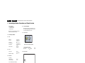
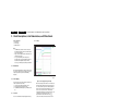
1. Technical Specifications, Connections, and Chassis Overview
1.2
Index of this chapter:
1.1 Technical Specifications
1.2 Connection Overview
1.3 Chassis Overview
Note: The following connector colour abbreviations are used
(acc. to DIN/IEC 757): Bk= Black, Bu= Blue, Gn= Green, Gy=
Grey, Rd= Red, Wh= White, and Ye= Yellow.
Note: Figures below can deviate slightly from the actual
situation, due to the different set executions.
1.1
Technical Specifications
1.1.1
Vision
Display type
Screen size
Tuning system
TV Colour systems
Video playback
Channel selections
1.1.2
Maximum power (WRMS)
1.1.3
:
:
:
:
:
:
:
:
:
1.2.1
CRT, DV, FSQ
14” (36 cm), 4:3
20” (51 cm), 4:3
PLL
NTSC M/N, PAL M
NTSC M/N 3.58, 4.43
PAL B/G
181 presets
Full-Cable
: FM-mono
: BTSC with SAP
: 1x3
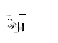
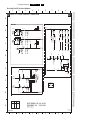
Front Connections
G_16560_006.eps
130706
Figure 1-1 Front connections (to be updated)
Cinch: Video CVBS - In, Audio - In
Ye - Video CVBS
1 VPP / 75 ohm
Wh - Audio
0.2 VRMS / 10 kohm
Sound
Sound systems
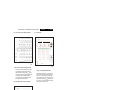
Connection Overview
1.2.2
jq
jq
Rear Connections
Miscellaneous
Power supply:
- Mains voltage (VAC)
- Mains frequency (Hz)
: 100-250
: 50 / 60
75 Ohm ANT.
Power consumption (values are indicative)
- Normal operation (W)
: 36 (14”)
: 46 (20”)
- Stand-by (W)
: <1
E_14560_015.eps
260204
Dimensions (WxHxD cm)
Weight (kg)
Ambient conditions:
- Temperature range (°C)
- Maximum humidity
: 36.2 x 35.0 x 35.4
(14”)
: 49.1 x 44.9 x 46.3
(20”)
: 8.7 (14”)
: 15.6 (20”)
: +5 to +40
: 90% R.H.
Figure 1-2 Rear connections (needs to be checked)
FM Ant
1 - F type
75 ohm, coax
D
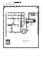
Technical Specifications, Connections, and Chassis Overview
1.3
L03.6L CA
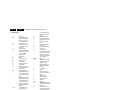
1.
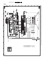
Chassis Overview
B1
CRT PANEL
MONO
CARRIER
POWER SUPPLY
A1
DEFLECTION
A2
TUNER IF
A3
IF, VIDEO PROCESSING, CONTROL,
AND SYNC.
A4
AUDIO BTSC STEREO DECODER
A5
AUDIO AMP + MONO SOUND PROC.
A6
FRONT I/O + FRONT CONTROL
+ HEADPHONE
A7
E_14560_013.eps
240304
Figure 1-3 Chassis overview
EN 3
EN 4
2.
L03.6L CA
Safety Instructions, Warnings, and Notes
2. Safety Instructions, Warnings, and Notes
1. Perform the “general repair instruction” noted above.
2. Clean the power supply and deflection circuitry on the
chassis.
3. Clean the picture tube panel and the neck of the picture
tube.
Index of this chapter:
2.1 Safety Instructions
2.2 Maintenance Instructions
2.3 Warnings
2.4 Notes
2.1
Safety Instructions
2.3
Safety regulations require the following during a repair:
• Connect the set to the Mains/AC Power via an isolation
transformer (> 800 VA).
• Replace safety components, indicated by the symbol h,
only by components identical to the original ones. Any
other component substitution (other than original type) may
increase risk of fire or electrical shock hazard.
• Wear safety goggles when you replace the CRT.
•
Safety regulations require that after a repair, the set must be
returned in its original condition. Pay in particular attention to
the following points:
• General repair instruction: as a strict precaution, we advise
you to re-solder the solder connections through which the
horizontal deflection current flows. In particular this is valid
for the:
1. Pins of the line output transformer (LOT).
2. Fly-back capacitor(s).
3. S-correction capacitor(s).
4. Line output transistor.
5. Pins of the connector with wires to the deflection coil.
6. Other components through which the deflection current
flows.
Note: This re-soldering is advised to prevent bad connections
due to metal fatigue in solder connections, and is therefore only
necessary for television sets more than two years old.
• Route the wire trees and EHT cable correctly and secure
them with the mounted cable clamps.
• Check the insulation of the Mains/AC Power lead for
external damage.
• Check the strain relief of the Mains/AC Power cord for
proper function, to prevent the cord from touching the CRT,
hot components, or heat sinks.
• Check the electrical DC resistance between the Mains/AC
Power plug and the secondary side (only for sets that have
a Mains/AC Power isolated power supply):
1. Unplug the Mains/AC Power cord and connect a wire
between the two pins of the Mains/AC Power plug.
2. Set the Mains/AC Power switch to the "on" position
(keep the Mains/AC Power cord unplugged!).
3. Measure the resistance value between the pins of the
Mains/AC Power plug and the metal shielding of the
tuner or the aerial connection on the set. The reading
should be between 4.5 Mohm and 12 Mohm.
4. Switch "off" the set, and remove the wire between the
two pins of the Mains/AC Power plug.
• Check the cabinet for defects, to prevent touching of any
inner parts by the customer.
2.2
Warnings
V
E_06532_007.eps
250304
Figure 2-1 Discharge picture tube
•
•
•
•
All ICs and many other semiconductors are susceptible to
electrostatic discharges (ESD w). Careless handling
during repair can reduce life drastically. Make sure that,
during repair, you are connected with the same potential as
the mass of the set by a wristband with resistance. Keep
components and tools also at this same potential. Available
ESD protection equipment:
– Complete kit ESD3 (small table mat, wristband,
connection box, extension cable and earth cable) 4822
310 10671.
– Wristband tester 4822 344 13999.
Be careful during measurements in the high voltage
section.
Never replace modules or other components while the unit
is switched "on".
When you align the set, use plastic rather than metal tools.
This will prevent any short circuits and prevents circuits
from becoming unstable.
2.4
Notes
2.4.1
General
•
Maintenance Instructions
We recommend a maintenance inspection carried out by
qualified service personnel. The interval depends on the usage
conditions:
• When a customer uses the set under normal
circumstances, for example in a living room, the
recommended interval is three to five years.
• When a customer uses the set in an environment with
higher dust, grease, or moisture levels, for example in a
kitchen, the recommended interval is one year.
• The maintenance inspection includes the following actions:
In order to prevent damage to ICs and transistors, avoid all
high voltage flashovers. In order to prevent damage to the
picture tube, use the method shown in figure “Discharge
picture tube”, to discharge the picture tube. Use a high
voltage probe and a multi-meter (position VDC). Discharge
until the meter reading is 0 V (after approx. 30 s).
•
•
Measure the voltages and waveforms with regard to the
chassis (= tuner) ground (H), or hot ground (I), depending
on the tested area of circuitry. The voltages and waveforms
shown in the diagrams are indicative. Measure them in the
Service Default Mode (see chapter 5) with a colour bar
signal and stereo sound (L: 3 kHz, R: 1 kHz unless stated
otherwise) and picture carrier at 475.25 MHz for PAL, or
61.25 MHz for NTSC (channel 3).
Where necessary, measure the waveforms and voltages
with (D) and without (E) aerial signal. Measure the
voltages in the power supply section both in normal
operation (G) and in stand-by (F). These values are
indicated by means of the appropriate symbols.
The semiconductors indicated in the circuit diagram and in
the parts lists, are interchangeable per position with the
Safety Instructions, Warnings, and Notes
•
2.4.2
Schematic Notes
•
•
•
•
•
•
2.4.3
semiconductors in the unit, irrespective of the type
indication on these semiconductors.
Manufactured under license from Dolby Laboratories.
“Dolby”, “Pro Logic” and the “double-D symbol”, are
trademarks of Dolby Laboratories.
All resistor values are in ohms, and the value multiplier is
often used to indicate the decimal point location (e.g. 2K2
indicates 2.2 kohm).
Resistor values with no multiplier may be indicated with
either an "E" or an "R" (e.g. 220E or 220R indicates 220
ohm).
All capacitor values are given in micro-farads (μ= x10-6),
nano-farads (n= x10-9), or pico-farads (p= x10-12).
Capacitor values may also use the value multiplier as the
decimal point indication (e.g. 2p2 indicates 2.2 pF).
An "asterisk" (*) indicates component usage varies. Refer
to the diversity tables for the correct values.
The correct component values are listed in the Spare Parts
List. Therefore, always check this list when there is any
doubt.
Rework on BGA (Ball Grid Array) ICs
General
Although (LF)BGA assembly yields are very high, there may
still be a requirement for component rework. By rework, we
mean the process of removing the component from the PWB
and replacing it with a new component. If an (LF)BGA is
removed from a PWB, the solder balls of the component are
deformed drastically so the removed (LF)BGA has to be
discarded.
Device Removal
As is the case with any component that is being removed, it is
essential when removing an (LF)BGA, that the board, tracks,
solder lands, or surrounding components are not damaged. To
remove an (LF)BGA, the board must be uniformly heated to a
temperature close to the reflow soldering temperature. A
uniform temperature reduces the risk of warping the PWB.
To do this, we recommend that the board is heated until it is
certain that all the joints are molten. Then carefully pull the
component off the board with a vacuum nozzle. For the
appropriate temperature profiles, see the IC data sheet.
Area Preparation
When the component has been removed, the vacant IC area
must be cleaned before replacing the (LF)BGA.
Removing an IC often leaves varying amounts of solder on the
mounting lands. This excessive solder can be removed with
either a solder sucker or solder wick. The remaining flux can be
removed with a brush and cleaning agent.
After the board is properly cleaned and inspected, apply flux on
the solder lands and on the connection balls of the (LF)BGA.
Note: Do not apply solder paste, as this has been shown to
result in problems during re-soldering.
Device Replacement
The last step in the repair process is to solder the new
component on the board. Ideally, the (LF)BGA should be
aligned under a microscope or magnifying glass. If this is not
possible, try to align the (LF)BGA with any board markers.
So as not to damage neighbouring components, it may be
necessary to reduce some temperatures and times.
More Information
For more information on how to handle BGA devices, visit this
URL: www.atyourservice.ce.philips.com (needs subscription,
not available for all regions). After login, select “Magazine”,
then go to “Repair downloads”. Here you will find Information
on how to deal with BGA-ICs.
2.4.4
L03.6L CA
2.
EN 5
Lead-free Solder
Philips CE is producing lead-free sets (PBF) from 1.1.2005
onwards.
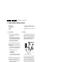
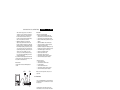
Identification: The bottom line of a type plate gives a 14-digit
serial number. Digits 5 and 6 refer to the production year, digits
7 and 8 refer to production week (in example below it is 1991
week 18).
MODEL
MADE IN BELGIUM
220-240V ~ 50/60Hz
128W
VHF+S+H+UHF
: 32PF9968/10
PROD.NO: AG 1A0617 000001
S
BJ3.0E LA
E_06532_024.eps
130606
Figure 2-2 Serial number example
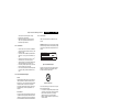
Regardless of the special lead-free logo (which is not always
indicated), one must treat all sets from this date onwards
according to the rules as described below.
P
b
Figure 2-3 Lead-free logo
Due to lead-free technology some rules have to be respected
by the workshop during a repair:
• Use only lead-free soldering tin Philips SAC305 with order
code 0622 149 00106. If lead-free solder paste is required,
please contact the manufacturer of your soldering
equipment. In general, use of solder paste within
workshops should be avoided because paste is not easy to
store and to handle.
• Use only adequate solder tools applicable for lead-free
soldering tin. The solder tool must be able:
– To reach a solder-tip temperature of at least 400°C.
– To stabilise the adjusted temperature at the solder-tip.
– To exchange solder-tips for different applications.
• Adjust your solder tool so that a temperature of around
360°C - 380°C is reached and stabilised at the solder joint.
Heating time of the solder-joint should not exceed ~ 4 sec.
Avoid temperatures above 400°C, otherwise wear-out of
tips will increase drastically and flux-fluid will be destroyed.
To avoid wear-out of tips, switch “off” unused equipment or
reduce heat.
• Mix of lead-free soldering tin/parts with leaded soldering
tin/parts is possible but PHILIPS recommends strongly to
avoid mixed regimes. If this cannot be avoided, carefully
clean the solder-joint from old tin and re-solder with new
tin.
• Use only original spare-parts listed in the Service-Manuals.
Not listed standard material (commodities) has to be
purchased at external companies.
• Special information for lead-free BGA ICs: these ICs will be
delivered in so-called "dry-packaging" to protect the IC
against moisture. This packaging may only be opened
shortly before it is used (soldered). Otherwise the body of
the IC gets "wet" inside and during the heating time the
structure of the IC will be destroyed due to high (steam-)
pressure inside the body. If the packaging was opened
before usage, the IC has to be heated up for some hours
(around 90°C) for drying (think of ESD-protection!).
Do not re-use BGAs at all!
• For sets produced before 1.1.2005, containing leaded
soldering tin and components, all needed spare parts will
be available till the end of the service period. For the repair
of such sets nothing changes.
EN 6
2.
L03.6L CA
Safety Instructions, Warnings, and Notes
In case of doubt whether the board is lead-free or not (or with
mixed technologies), you can use the following method:
• Always use the highest temperature to solder, when using
SAC305 (see also instructions below).
• De-solder thoroughly (clean solder joints to avoid mix of
two alloys).
Caution: For BGA-ICs, you must use the correct temperatureprofile, which is coupled to the 12NC. For an overview of these
profiles, visit the website www.atyourservice.ce.philips.com
(needs subscription, but is not available for all regions)
You will find this and more technical information within the
"Magazine", chapter "Repair downloads".
For additional questions please contact your local repair help
desk.
2.4.5
Alternative BOM identification
In September 2003, Philips CE introduced a change in the way
the serial number (or production number, see Figure 2-2) is
composed. From this date on, the third digit in the serial
number (example: AG2B0335000001) indicates the number of
the alternative BOM (Bill of Materials used for producing the
specific model of TV set). It is possible that the same TV model
on the market is produced with e.g. two different types of
displays, coming from two different O.E.M.s.
By looking at the third digit of the serial number, the service
technician can see if there is more than one type of B.O.M.
used in the production of the TV set he is working with. He can
then consult the At Your Service Web site, where he can type
in the Commercial Type Version Number of the TV set (e.g.
28PW9515/12), after which a screen will appear that gives
information about the number of alternative B.O.M.s used.
If the third digit of the serial number contains the number 1
(example: AG1B033500001), then there is only one B.O.M.
version of the TV set on the market. If the third digit is a 2
(example: AG2B0335000001), then there are two different
B.O.M.s. Information about this is important for ordering
the correct spare parts!
For the third digit, the numbers 1...9 and the characters A...Z
can be used, so in total: 9 plus 26 = 35 different B.O.M.s can
be indicated by the third digit of the serial number.
2.4.6
Practical Service Precautions
•
•
It makes sense to avoid exposure to electrical shock.
While some sources are expected to have a possible
dangerous impact, others of quite high potential are of
limited current and are sometimes held in less regard.
Always respect voltages. While some may not be
dangerous in themselves, they can cause unexpected
reactions that are best avoided. Before reaching into a
powered TV set, it is best to test the high voltage insulation.
It is easy to do, and is a good service precaution.
Directions for Use
3. Directions for Use
You can download this information from the following websites:
http://www.philips.com/support
http://www.p4c.philips.com
L03.6L CA
3.
EN 7
EN 8
4.
Mechanical Instructions
L03.6L CA
4. Mechanical Instructions
4.3
Index of this chapter:
4.1 Rear Cover Removal
4.2 Service Position Main Panel
4.3 Rear Cover Mounting
4.1
Rear Cover Removal
1. Remove all fixation screws of the rear cover.
2. Now pull the rear cover in backward direction to remove it.
4.2
Service Position Main Panel
1. Disconnect the strain relief of the AC power cord.
2. Remove the main panel, by pushing the two centre clips
outward [1]. At the same time pull the panel away from the
CRT [2].
3. If necessary, disconnect the degaussing coil by removing
the cable from the (red) connector 1512.
4. Move the panel somewhat to the left and flip it 90 degrees
[3], with the components towards the CRT.
1
1
2
A
3
B
Figure 4-1 Service Position
G_16560_008.eps
130706
Rear Cover Mounting
Before you mount the rear cover, perform the following checks:
1. Check whether the mains cord is mounted correctly in its
guiding brackets.
2. Re-place the strain relief of the AC power cord into the
cabinet.
3. Check whether all cables are replaced in their original
position
Service Modes, Error Codes, and Fault Finding
L03.6L CA
5.
EN 9
5. Service Modes, Error Codes, and Fault Finding
•
•
Index of this chapter:
5.1 Test Points
5.2 Service Modes
5.3 Problems and Solving Tips
5.4 Service Tools
5.5 Error Codes
5.6 The Blinking LED Procedure
5.7 Protections
5.8 Repair Tips
5.1
Test Points
This chassis is equipped with test points in the service printing.
In the schematics test points are identified with a rectangle box
around Fxxx or Ixxx. On the PCB, test points are specifically
mentioned in the service manual as “half moons” with a dot in
the centre.
Perform measurements under the following conditions:
• Service Default Alignment Mode.
• Video: colour bar signal.
• Audio: 3 kHz left, 1 kHz right.
5.2
Service Modes
Service Default Alignment Mode (SDAM) offers several
features for the service technician.
There is also the option of using ComPair, a hardware interface
between a computer (see requirements below) and the TV
chassis. It offers the ability of structured trouble shooting, test
pattern generation, error code reading, software version readout, and software upgrading.
Minimum Requirements: a Pentium Processor, Windows 95/
98, and a CD-ROM drive (see also paragraph “ComPair”).
•
•
•
•
•
Bass, treble and balance at 50%; volume at 25%.
All service-unfriendly modes (if present) are disabled, like:
– (Sleep) timer,
– Child/parental lock,
– Blue mute,
– Hotel/hospitality mode
– Auto switch-off (when no “IDENT” video signal is
received for 15 minutes),
– Skip / blank of non-favourite presets / channels,
– Auto store of personal presets,
– Auto user menu time-out.
Operation hours counter.
Software version.
Option settings.
Error buffer reading and erasing.
Software alignments.
How to enter SDAM
Use one of the following methods:
• Use a standard customer RC-transmitter and key in the
code 062596 directly followed by the “M” (menu) button or
• Short jumper wires 9448 and pin 4 of 7200 on the mono
carrier (see Fig. 8-1) and apply AC power. Then press the
power button (remove the short after start-up).
Caution: Entering SDAM by shortening wires 9448 and pin
4 of 7200 will override the +8V-protection. Do this only for
a short period. When doing this, the service-technician
must know exactly what he is doing, as it could lead to
damaging the set.
• Or via ComPair.
After entering SDAM, the following screen is visible, with S at
the upper right side for recognition.
L L L L
A A A B C D
X . Y
E R R
X X
X X
X X
X X
X X
X X X
X X X
X X X
X X X
X X X
Table 5-1 SW Cluster
SW
Cluster
Software
name
UOC type
L06SP
L036LM x.y
TDA9370
C
O
A
T
W
G
UOC
Special
Diversity Features
55K
Mono
ROM Size
L
P
K
U
H
E
E
T
B
N
I
O
S
X X X
X X X
A R
I O N S
C L E A R
>
?
E R
T E
T O N E
M E T R Y
>
>
>
Abbreviations in Software name:
U = Nafta, M = Mono, N = Stereo.
5.2.1
G_16560_007.eps
130706
Service Default Alignment Mode (SDAM)
Figure 5-1 SDAM menu (example)
Purpose
• To change option settings.
• To create a predefined setting to get the same
measurement results as given in this manual.
• To display / clear the error code buffer.
• To override SW protections.
• To perform alignments.
• To start the blinking LED procedure.
•
•
Specifications
Table 5-2 SDM default settings
•
Region
Freq. (MHz)
Default
system
Europe, AP-PAL/Multi
475.25
PAL B/G
NAFTA, AP-NTSC, LATAM
61.25 (ch. 3)
NTSC M
•
0
All picture settings at 50% (brightness, colour contrast,
hue).
•
•
•
•
LLLL. This is the operation hours counter. It counts the
normal operation hours, not the stand-by hours.
AAABCD-X.Y. This is the software identification of the
main micro controller:
– A = the project name (L03 2006).
– B = the region: E= Europe, A= Asia Pacific, U= NAFTA,
L= LATAM.
– C = the feature of software diversity: N = stereo nonDBX, S = stereo dBx, M = mono, D = DVD
– D = the language cluster number:
– X = the main software version number.
– Y = the sub software version number.
S. Indication of the actual mode. S= SDAM= Service
Default Alignment mode.
Error buffers. Five errors possible.
Option bytes. Seven codes possible.
Clear. Erase the contents of the error buffer. Select the
CLEAR menu item and press the CURSOR RIGHT key.
The content of the error buffer is cleared.
Options. To set the Option Bytes. See chapter 8.3.1 for a
detailed description.
EN 10
•
•
•
•
5.
L03.6L CA
Service Modes, Error Codes, and Fault Finding
Snowy picture
• No or bad antenna signal. Connect a proper antenna
signal.
• Antenna not connected. Connect the antenna.
• No channel / pre-set is stored at this program number. Go
to the INSTALL menu and store a proper channel at this
program number.
• The tuner is faulty (in this case the CODES line will contain
error number 10). Check the tuner and replace / repair if
necessary.
AKB. Disable (0) or enable (1) the “black current loop”
(AKB = Auto Kine Bias).
Tuner. To align the Tuner. See chapter 8.3.2 for a detailed
description.
White Tone. To align the White Tone. See chapter 8.3.3
for a detailed description.
Geometry. To align the set geometry. See chapter 8.3.4
for a detailed description.
How to navigate
• In SDAM, select menu items with the CURSOR UP/DOWN
key on the remote control transmitter. The selected item
will be highlighted. When not all menu items fit on the
screen, move the CURSOR UP/DOWN key to display the
next / previous menu items.
• With the CURSOR LEFT/RIGHT keys, it is possible to:
– Activate the selected menu item.
– Change the value of the selected menu item.
– Activate the selected submenu.
• When you press the MENU button twice, the set will switch
to the normal user menus (with the SDAM mode still active
in the background). To return to the SDAM menu press the
OSD / STATUS button.
• When you press the MENU key in a submenu, you will
return to the previous menu.
How to store settings
To store settings, leave the SDAM mode with the Stand-by
button on the remote.
Snowy picture and/or unstable picture
• A scrambled or decoded signal is received.
Black and white picture
Increase the COLOR value when:
• The picture improves after you have pressed the “Smart
Picture” button on the remote control.
The new “Personal” preference value is automatically stored.
Menu text not sharp enough
Decrease the CONTRAST value when:
The picture improves after you have pressed the “Smart
Picture” button on the remote control.
The new “Personal” preference value is automatically stored.
5.3.2
No sound or sound too loud (after channel change /
switching on)
Increase / decrease the VOLUME level.
Press the Smart Sound button repeatedly to access 4 different
types of sound settings and choose your desired setting.
How to exit
Switch the set to STANDBY by pressing the power button on
the remote control (if you switch the set 'off' by removing the AC
power, the set will return in SDAM when AC power is reapplied). The error buffer is not cleared.
5.3
Problems and Solving Tips
5.3.1
Picture Problems
Note: Below described problems are all related to the TV
settings. The procedures to change the value (or status) of the
different settings are described.
No colours / noise in picture
1. Press the MENU button on the remote control.
2. Select the INSTALLATION sub menu.
3. Select and change the SYSTEM setting until picture and
sound are correct.
4. Select the STORE menu item.
Colours not correct / unstable picture
1. Press the MENU button on the remote control.
2. Select the INSTALLATION sub menu.
3. Select and change the SYSTEM setting until picture and
sound are correct.
4. Select the STORE menu item.
Picture too dark or too bright
Increase / decrease the BRIGHTNESS and / or the
CONTRAST value when:
• The picture improves after you have pressed the “Smart
Picture” button on the remote control.
• The picture improves after you have switched on the
Customer Service Mode
The new “Personal” preference value is automatically stored.
White line around picture elements and text
Decrease the SHARPNESS value when:
• The picture improves after you have pressed the “Smart
Picture” button on the remote control.
The new “Personal” preference value is automatically stored.
Sound Problems
5.4
Service Tools
5.4.1
ComPair
Introduction
ComPair (Computer Aided Repair) is a service tool for Philips
Consumer Electronics products. ComPair is a further
development on the European DST (service remote control),
which allows faster and more accurate diagnostics. ComPair
has three big advantages:
1. ComPair helps you to quickly get an understanding on how
to repair the chassis in a short time by guiding you
systematically through the repair procedures.
2. ComPair allows very detailed diagnostics (on I2C level) and
is therefore capable of accurately indicating problem areas.
You do not have to know anything about I2C commands
yourself because ComPair takes care of this.
3. ComPair speeds up the repair time since it can
automatically communicate with the chassis (when the
microprocessor is working) and all repair information is
directly available. When ComPair is installed together with
the Force/SearchMan electronic manual of the defective
chassis, schematics and PWBs are only a mouse click
away.
Specifications
ComPair consists of a Windows based fault finding program
and an interface box between PC and the (defective) product.
The ComPair interface box is connected to the PC via a serial
(or RS-232) cable.
For this chassis, the ComPair interface box and the TV
communicate via a bi-directional service cable via the service
connector(s).
The ComPair fault finding program is able to determine the
problem of the defective television. ComPair can gather
diagnostic information in two ways:
• Automatically (by communicating with the television):
ComPair can automatically read out the contents of the
Service Modes, Error Codes, and Fault Finding
entire error buffer. Diagnosis is done on I2C/UART level.
ComPair can access the I2C/UART bus of the television.
ComPair can send and receive I2C/UART commands to
the microcontroller of the television. In this way, it is
possible for ComPair to communicate (read and write) to
devices on the I2C/UART buses of the TV-set.
• Manually (by asking questions to you): Automatic
diagnosis is only possible if the microcontroller of the
television is working correctly and only to a certain extent.
When this is not the case, ComPair will guide you through
the fault finding tree by asking you questions (e.g. Does the
screen give a picture? Click on the correct answer: YES /
NO) and showing you examples (e.g. Measure test-point I7
and click on the correct oscillogram you see on the
oscilloscope). You can answer by clicking on a link (e.g.
text or a waveform picture) that will bring you to the next
step in the fault finding process.
By a combination of automatic diagnostics and an interactive
question / answer procedure, ComPair will enable you to find
most problems in a fast and effective way.
TO
I2C SERVICE
CONNECTOR
VCR
Power
9V DC
EN 11
ComPair order codes (US):
• ComPair Software: ST4191.
• ComPair Interface Box: 4822 727 21631.
• AC Adapter: T405-ND.
• ComPair Quick Start Guide: ST4190.
• ComPair interface extension cable: 3139 131 03791.
• ComPair UART interface cable: 3122 785 90630.
Note: If you encounter any problems, contact your local
support desk.
5.5
PC
5.
How to Order
ComPair order codes (EU/AP/LATAM):
• Starter kit ComPair32/SearchMan32 software and
ComPair interface (excl. transformer): 3122 785 90450.
• ComPair interface (excl. transformer): 4822 727 21631.
• Starter kit ComPair32 software (registration version): 3122
785 60040.
• Starter kit SearchMan32 software: 3122 785 60050.
• ComPair32 CD (update): 3122 785 60070 (year 2002),
3122 785 60110 (year 2003 onwards).
• SearchMan32 CD (update): 3122 785 60080 (year 2002),
3122 785 60120 (year 2003), 3122 785 60130 (year 2004).
• ComPair firmware upgrade IC: 3122 785 90510.
• Transformer (non-UK): 4822 727 21632.
• Transformer (UK): 4822 727 21633.
• ComPair interface cable: 3122 785 90004.
• ComPair interface extension cable: 3139 131 03791.
• ComPair UART interface cable: 3122 785 90630.
How to Connect
This is described in the chassis fault finding database in
ComPair.
TO
UART SERVICE
CONNECTOR
L03.6L CA
Error Codes
In case of non-intermittent faults, clear the error buffer before
you begin the repair. These to ensure that old error codes are
no longer present.
I2C
E_06532_021.eps
180804
If possible, check the entire contents of the error buffer.
In some situations, an error code is only the result of another
error code and not the actual cause (e.g., a fault in the
protection detection circuitry can also lead to a protection).
Figure 5-2 ComPair interface connection
Table 5-3 Error Code Table
ERROR Device
Error description
Check item
Diagram
0
Not applicable
No Error
-
-
1
Not applicable
X-Ray Protection (USA)
7421, 2423, 6421, 6422
A2
2
Not applicable
Horizontal Protection
7421, 7422, 7423
A2
3
Not applicable
Vertical Protection
7461, 7462, 7463, 7464, 7465, 7466
A2
4
TDA9853H
Tone control & Audio processor I2C
identification error
7861 (Stereo/Sap)
A5
5
TDA93XX
POR 3.3V / 8V Protection
7200, 7541, 7491, 7493, 7496
A4, A1
6
I2C bus
General I2C bus error
7200, 3604, 3605
A4
7
Not applicable
-
-
-
8
Not applicable
E/W Protection (Large Screen)
-
-
9
M24C16
NVM I2C identification error
7641, 3641, 3642, 3643
A4
10
Tuner
Tuner I2C identification error
1000, 3003, 3004
A3
11
Not applicable
Black current loop protection
3313, 7307, 7308, 7309, 7310, 7311, 7312, 7313,
7314, 7315, 7316, 7317, 7318, CRT
B1
12
Not applicable
MAP I2C identification error (USA)
-
-
13
Not applicable
VC I2C identification error (EU)
-
-
14
Not applicable
DVD I2C identification error
-
-
Due to system constraints, the error 2 code indication for 14”
and 20” is different. So the error “Horizontal Protection” (error
2 code) is as follows:
• 14” (error code = 2 and 10)
• 20” (error code = 5 and 10)
EN 12
5.6
5.
L03.6L CA
Service Modes, Error Codes, and Fault Finding
The Blinking LED Procedure
Via this procedure, you can make the contents of the error
buffer visible via the front LED. This is especially useful when
there is no picture.
When the SDAM is entered, the LED will blink the contents of
the error-buffer.
• n short blinks (n = 1 - 14),
• When all the error-codes are displayed, the sequence
finishes with a LED blink of 3 s,
• The sequence starts again.
Example of error buffer: 12 9 6 0 0
After entering SDAM:
• 12 short blinks followed by a pause of 3 s,
• 9 short blinks followed by a pause of 3 s,
• 6 short blinks followed by a pause of 3 s,
• 1 long blink of 3 s to finish the sequence,
• the sequence starts again.
5.7
Protections
If a fault situation is detected an error code will be generated
and if necessary the set will be put in the protection mode.
Blinking of the red LED at a frequency of 3 Hz indicates the
protection mode. In some error cases, the microprocessor
does not put the set in the protection mode. The error codes of
the error buffer can be read via the service menu (SDAM), the
blinking LED procedure or via ComPair.
To get a quick diagnosis the chassis has one service modes
implemented:
• The Service Default Alignment Mode (SDAM). Start-up of
the set in a predefined way and adjustment of the set via a
menu and with the help of test patterns.
5.8
Repair Tips
Below some failure symptoms are given, followed by a repair
tip.
• Set is dead and makes hiccupping sound. “Main
Supply” is available. Hiccupping stops when de-soldering
L5563, meaning that problem is in the “Main Supply” line.
No output voltages at LOT, no horizontal deflection.
Reason: line transistor 7421 is defective.
• Set is dead, and makes no sound. Check power supply
IC 7520. Result: voltage at pins 2, 6, 7, 9 and 11 are about
180 V and pin 14 is 0 V. The reason why the voltage on
these pins is so high is because the output driver (pin 11)
has an open load. That is why MOSFET 7521 is not able to
switch. Reason: feedback resistor 3523 is defective.
Caution: be careful measuring on the gate of 7521;
circuitry is very high ohmic and can easily be damaged!
• Set is in hiccup mode and shuts down after 8 s. Blinking
LED (set in SDM mode) indicates error 5. As it is unlikely
that the “POR” and “+8V protection” happen at the same
time, measure the “+8V”. If this voltage is missing, check
transistor 7491 and 7496.
• Set is non-stop in hiccup mode. Set is in over current
mode; check the secondary sensing (opto coupler 7515)
and the “Main Supply” voltage. Signal “Stdby_con” must be
logic low under normal operation conditions and goes to
high (3.3 V) under stand-by and fault conditions.
• Set turns on, but without picture and sound. The screen
shows snow, but OSD and other menus are okay. Blinking
LED procedure indicates error 11, so problem is expected
in the tuner (pos. 1000). Check presence of supply
voltages. As “Vlotaux+5V” at pin 5 and 7 are okay,
“VT_supply” at pin 9 is missing. Conclusion: resistor 3449
and 3450 are defective
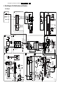
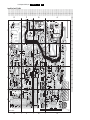
Block Diagrams, Test Point Overviews, and Waveforms
L03.6L CA
6.
13
6. Block Diagrams, Test Point Overviews, and Waveforms
Block Diagram
A7
A5
FRONT I/O
MONO
SY_CVBS_IN
7901 AN7522N (STEREO)
7902 AN7523N (MONO)
1
7861
TDA9853H
V
V
A7
A6 AUDIO AMPLIFIER
AUDIO PROCESSING (BTSC STEREO DECODER)
STEREO
5
L1_IN
L
A5
L1_IN
INPUT
SELECT
A8
R1_IN
R1_IN
R
6
4
8
L-
5
R-
1
F1
IR
IR
+3V3
62
9
L
A4
10
IIC
BUS
A11
1
6909
KEYBOARD
R+ 2
12
LOCAL
KEYBOARD
R
8
FILAMENT
A3
A1
BTSC STEREO
+
DECODER
4
SCL
3866
18
A7
SDA
3865
A2
ERR
4
ROM
RAM
HEADPHONE
L+
L+
L-
L-
R-
R-
R+
R+
4
TELE
TEXT/CC
+
OSD
VOLUME A6
SDAM
9625
CVBS SYNC
57
A4 IF, VIDEO PROCESSING
B1 CRT
6001
BZX79-C33
AM_FM_MONO
1621
12MHz
58
+170V0
IF
1001
23
VIF_1
VIDEO
IF
AGC
11
VIF_2
24
ERR
10
VIDEO
PLL
DEMOD.
VIDEO
AMPLIFIER
38
7201
5
4
3003
AGC
1
3004
SOUND
FM-DEMOD.
DE-EMPH.
TUNER_AGC
A4 SDA
1201
40
4.5MHz
AUDIO
SWITCH
V1
SOUND
AMPL.
+ AVL
+8V
N.C.
VIDEO
FILTERS
43
42
A5 L1_IN
A7
VIDEO
IDENT
SY_CVBS_IN
7202
A4 SCL
Y
Y-DELAY
44
35
1003
1 SDA
RGB
MATRIX
I/O
SWITCHING
PAL/NTSC
DECODER
R-Y
BASE
BAND
DELAY
B-Y
U
V
3203
3
N.C.
A1 POWER SUPPLY
1512
4
1515
R_SC1_IN_V_IN
G_SC1_IN_Y_IN
B_SC1_IN_U_IN
FBL_SC1_IN
OSD/TEXT/CC
INSERT
53
BLACK
STRETCH
BLUE
STRETCH
49
WHITE
STRETCH
WHITE-P.
ADJ
B
3620
V10
1622
1
RED
3621 V11
1
t
1300
1
GREEN
2
2
BLUE
3
3
V13
V14
3305
G
3309
7312
7317
7318
V15
V16
V17
0165
BEAM-LIMIT A2
BLK_IN
3624
4
4
5
5
AQUADAG
R
7
G
9
R
B
3
G
CRT
(9P)
B
4
B
5
6 8
3319
VG2
6
50
FRAME_OUT
7
A2
FOCUS
25kV
EHT
3318
6318
+170V0
FILAMENT
8
A2 DEFLECTION
LINE
Hflybk
RESERVED
7580
ENERGIZING
CIRCUIT
(optional)
3503
2
RGB
INSERT
51
52
46 47 48 45
A4 SYNC.
Degaussing
Coil
G
V9
(MONO)
2 SCL
3
RGB
CONTROL
R
3619
3301
7310
7315
7316
OSD
3205
27
3313
R
7200-D
TDA93XX
-12V
5441
34
EHT
1
3424
-12V
EHT
FOCUS
D3
VIDEO
INTERNAL
5421
7421
BUT11APX
7
2423
TV TUNER
T1
7308
7313
7314
7200-C
TDA93XX
AUDIO CARRIER
FILTER
5201
7200-A
TDA93XX
6422
9
VT
2
V12
+8VD
1000
UV1336
6, 7
VG2
7423
90VAC-130VAC
low range
1511
Std_Con A1
VT_SUPPLY_A A2
+5V
ComPair
CONN.
A3
A5
SCL
1
CPU
VT_SUPPLY
SCL
1/10
PAGES
MEMORY
SPEAKER
2 X 5W
16 Ohm
2 X 3W
8 Ohm
2 X 1W
8 Ohm
A3 TUNER IF
3642
SDA
V7
VST
PWMDAC
POWER (USA only)
38
3604
2
3643
3601
SDA
V8
CHANNEL + / VOLUME + / -
3911
3602
3605
3
I/O
PORTS
+3.3V
EEPROM 8
(NVM)
7
6
ERR
5
9
WP
11
1
A10
VOLUME
A4
1900
L+ 4
2
7641
M24C04
5601 5603 5602
7200-B
TDA93XX 54
61
56
6692
TSOP1836
+5V
A9
2906
+3.3V
Vaudio
3901
A8
2904
A7
Main_OutR
Main_OutR
18
26
A6
Main_OutL
Main_OutL
1
8
L
A4 CONTROL
FRONT CONTROL
2
7422
5502
H
H/V SYNC
SEPERATOR
V
H-OSC
+PLL
1500
6500
6501
5520
P1
1
T4E
6502
2504
6503
2
6562
11
7520
TEA1506
3506
DRIVER
P4
2
Vcc
SENSE
9
3525
S
6520
8
P5
3423
DEMAG
3528
CONTROL
IC
2406
9
5401
3549
3543
FRAME
V-DRVE
+
GEOMETRY
3522
21
V-DRIVE -
3581
EHT0
7540, 6540
6522
4
REFERENCE
CIRCUIT
1
7515
TCET1103
3
2
+3V3A
COLD GROUND
3544
EHT
A2
7451
7541
STANDBY
CIRCUIT
HOT GROUND
A2
Std_Con
A4
7464
5
D7
3463
7461
A4
1400
1
+160VD
D8
+160VD
2
3
6446
D9
3445
VT SUPPLY A3
FILAMENT
-12V
3443
6448
3444
6444
D10
FILAMENT A6
A2
6461
7466
4
3470
7462
7465
36
A4
BEAMLIMIT
3459
D4
V-DRIVE +
6452
3448
3402
8
6
6447
A1
6451
2455
HOR.
DEFL.
COIL
EHT
EHT 0
3410
3451
4
6423
22
CTRL
3403
A1
7523
7
MAINSUPPLY
Vaudio
7
6
0221
1
P3
6560
VG2
3447
Vaudio
A2
5560
5
3526
2521
3425
FILAMENT
3
G
P6
FOCUS
10
D1
2428
MAIN SUPPLY
D
3523
D2
V2
10
7521
11
H-DRIVE
5563
6561
14
DRAIN
33
P2
5562
3527
H-DRIVE
2nd LOOP
H-SHIFT
3446
2460
6463
6462
7463
EW
+
GEOMETRY
2465
1402
1
D5
20
3465
3464
2490
-12V
3474
2
3475
VERT.
DEFL.
COIL
FRAME OUT A4
E_14560_017.eps
240304
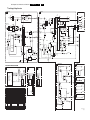
Block Diagrams, Test Point Overviews, and Waveforms
L03.6L CA
6.
14
I2C and Supply Voltage Overview
A1 POWER SUPPLY
A2 DEFLECTION
Degaussing
Coil
4
1515
ENERGIZING
CIRCUIT
(optional)
3503
2
t
RESERVED
7580
1
-12V
H-DRIVE
7421
BUT11APX
FOCUS
7
VG2
VG2
2
7422
1500
6500
5520
6501
6502
2504
6503
2
6562
5563
2
Vcc
SENSE
9
MAINSUPPLY
D
3523
3
G
6560
5560
8
S
3525
1x
2x
Vaudio
5
HOR.
DEFL.
COIL
6
6520
3549
7
FILAMENT
FRAME
7523
CTRL DEMAG 7
+160VD
VT SUPPLY
3463
3528
3581
CONTROL
IC
7461
7515
TCET1103
3444
6444
3446
2460
7465
3x
FILAMENT A6
6463
EHT
A2
7451
2
3
-12V
6448
FILAMENT
2x
6462
7463
3544
1
4
3470
7462
REFERENCE
CIRCUIT
4
1x
A3
6461
7466
V-DRIVE+
7540, 6540
6522
VT SUPPLY
-12V
3443
5
3522
FILAMENT
3445
6446
7464
To VIDEO
OUTPUTS
FILAMENT
3402
V-DRIVE6
8
3459
5401
3543
A4
3
3448
6447
9
EHT 0
2
BEAM- A4
LIMIT
6452
6423
8
3526
2521
2406
3423
A1
3313
6451
2455
10
7521
3451
4
6561
3527
7520
14
TEA1506
DRAIN
11
DRIVER
MAINSUPPLY
3403
EHT
7
3410
3447
0221
1
5562
11
3506
3425
Vaudio
+160VD
10
2428
1
VG2
170 V0
1300
1400
FOCUS
T4E
EHT
EHT
FOCUS
7423
5502
EHT
1
3424
-12V
5421
90VAC-130VAC
low range
1511
CRT
5441
-12V
2423
3
6422
1512
B1
3464
+3V3A
+3V3A
2465
1402
1
3465
2
3475
FRAME OUT A4
VERT.
DEFL.
COIL
3474
7541
Std_Con
STANDBY
CIRCUIT
A4
-12V
HOT GROUND
COLD GROUND
A4
B1
I2C BUS INTERCONNECTION DIAGRAM
Vaudio
A4 VIDEO PROCESSING
A3
PART OF
VIDEOPROCESSOR
TDA93XX
3604
+3.3V
3642
SCL
5
3644
11
WP
SDA
SCL
SCL
3003
2
6
M24C16
7 EEPROM
(NVM)
4491
VT Supply-A
A1
+3V3A
In
TDA9853H
AUDIO
PROC.
A2
FILAMENT
A5
AUDIO PROCESSING
5861
+ 8V
3495
7494
+5V
ERR
4
ERR
10
1x
2x
40
7861
TUNER
UV1336
ERR
9
6001
-/C33
6491
38
5 4
1000
7641
VT supply
+3V3
Vaudio
SDA
3865
3605
+5V
VT supply
3
1
3866
3601
3643
SET
PROCESSOR
SDA
ERR
6
TUNER IF
+5V
3494
7493
DECODER
(economic)
+3.3V
3602
3
A5 AUDIO BTSC STEREO
TUNER IF
3004
+3.3V
7200-B
A3
VIDEO PROCESSING
41 - 7861
1x
1x
A6
AUDIO AMPLIFIER
1 - 7901
or
1 - 7902
Vaudio
3496
ERROR CODE LIST
Error
0
1
2
Device
Not applicable
Not applicable
Not applicable
Error description
No Error
X-Ray Protection (USA)
Horizontal Protection
3
Not applicable
4
TDA9853H
Vertical Protection
Tone control & Audio processor I2C
identification error
Check item
7421, 2423, 6421, 6422
7421, 7422, 7423
7461, 7462, 7463, 7464, 7465,
7466
Diagram
A2
A2
7861 (Stereo/Sap)
A5
A2
3497
1003
1
+ 5V
FOR
COMPAIR
ONLY
3
6492
FILAMENT
FILAMENT
+8V
A7
4379
7496
5
6
7
8
9
10
11
12
13
14
TDA93XX
I2C bus
Not applicable
Not applicable
M24C16
Tuner
Not applicable
Not applicable
Not applicable
Not applicable
POR 3.3V / 8V Protection
General I2C bus error
E/W Protection (Large Screen)
NVM I2C identification error
Tuner I2C identification error
Black current loop protection
MAP I2C identification error (USA)
VC I2C identification error (Eu)
DVD I2C identification error
7200, 7541, 7491, 7493, 7496
7200, 3604, 3605
7641, 3641, 3642, 3643
1000, 3003, 3004
3313, 7307, 7308, 7309, 7310,
7311, 7312, 7313, 7314, 7315,
7316, 7317, 7318, CRT
-
A4, A1
A4
A4
A3
+8V
3493
7491
1x
AUDIO FRONT I/O
+ 3V3A
+3V3A
5482
+8VD
VTSupply-A
B1
-
+ 5V
2
3491
3492
F_15380_001.eps
050405
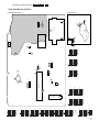
Block Diagrams, Test Point Overviews, and Waveforms
L03.6L CA
6.
15
Testpoint Overview Mono Carrier and CRT Panel
MONO CARRIER TRACK SIDE VIEW
CRT TRACK SIDE VIEW
7521
D
V16
6461
7520
D9
S
V15
G
2
P6
8
3
P4
LOT
2
9
7
D1
10
11
6
8
5441
3
5
V17
4
9
1302
1
6
P1
1
10
1300
6447
3 2 1
D8
1
V14
8
5520
6692
3
T et
CR ock
S
V13
F1
6560
V12
7
11
P3
V12
V13
6561
P2
HOT
1V / div DC
20µs / div.
COLD
V14
1V / div DC
20µs / div.
V15
7421
D2
B
D3
E
C
V8
1V / div DC
20µs / div.
3643
V7
3642
V2
V16
1000
3602
3601
AUDIO
PROC.
33
34
50V / div DC
20µs / div.
23
1
A4
V11
V10
V9
1622
5
4
3
2
1
E B C
7464
D6
B
7200
E
D7
C
VIDEO
PROC.
V2
21
D5
22
D4
0,5V / div DC
20µs / div.
1000
11
64
1
TUNER
D2
A5
D3
D4
D5
V9
32
D6
D7
D8
D9
D10
F1
0.5V / div DC
1ms / div.
0.5V / div DC
20µs / div.
V10
1V / div DC
20µs / div.
P1
V8
0,5V / div DC
20µs / div.
V11
1V / div DC
20µs / div.
P5
P6
T1
P2 97V DC
P3 13V5 DC
P4 17V8 DC
D1 97V DC
0.5V / div DC
1ms / div.
V7
T1
1V / div DC
20µs / div.
A4
50V / div DC
20µs / div.
7463
18
12
V17
3 D10
2
1
1
7861
A5
50V / div DC
20µs / div.
5V / div AC
20µs / div.
100V / div DC
20µs/div.
0.5V / div DC
5ms / div.
0.5V / div DC
5ms / div.
1V / div AC
5ms / div.
20V / div DC
5ms / div.
50V / div DC
20µs / div.
10V / div DC
20µs / div.
2V / div DC
20µs / div.
1V / div AC
2ms / div.
50V / div DC
5µs / div.
100V / div DC
5µs / div.
2V / div DC
5µs / div.
200mV / div AC
20µs / div.
E_14560_019.eps
180304
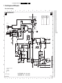
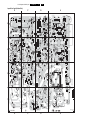
Circuit Diagrams and PWB Layouts
L03.6L CA
7.
16
7. Circuit Diagrams and PWB Layouts
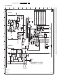
Mono Carrier: Power Supply
1
2
A1
3
4
5
6
7
8
9
10
11
POWER SUPPLY
A1
A
RES
For Relay Cct.
-12V
3
*
4
1515
G5PA-1-2 12VDC
Item
14V
20V
2503
2562
2453
3456
100U
680P
-
150U
470P
2N2
47K
A
2
-T
3
5500
*
BAS316
47K
6580
3580
2515
1520
I505
4R7
RES
1N5062
2507
6503
2503
1N5062
F514
To 1004 of
C
1n5
3508
1M5
2500
V
1
4
2
470n
3505
F505 T4E.250V
4
2
2
1
3
DMF24
1
RE_ADDED1
4
9501
RE_ADDED2
3
2581
6562
14
5515
10
6
5560
6560
50R
SB340
2560
2n2
5520
9509
S-GND
7540
7V4 BC847B
9V1
470n
2540
6520
I521 8V1
I520
HOT
COLD
3454
10K
7541
9V1
PDTC114ET
*
EHT
2453
820K
I527
3456
4n7
47K
A2
*
I526
Std_Con
3V3
A4
F504
..V..
(..V..)
G
+3V3A
3V3
BZX384-C3V3
100K
I522
470R
82n
3452
F444
15n
3541
6564
G
BC857B
8V8
3453
3545
8V0
7451
3546
I519
4n7
3528
15R
2
3
2541
2528
2K2
0R22
2n2
2452
4K7
1
F
I525
15K
3544
4
6V9
3548
7515
TCET1103(G)
I514
UDZS-6V2
6540
2K7
2K7
3582
3530
100n
6V3
2527
470p
F
1R0
3527
3543
3549
3
I523
2524
3526
E
I524
BZX384-C9V1
2583
1K0
6541
3524
6523
7
3542
BZX384-C6V2
6522
6
0V6
BAS316
OCP
BD
50R
AudioSupplyGnd_A
AudioSupplyGnd
15R
2525
1V3
FB
1K0
SS
OLP
47K
1u0
3520
1n0
2526
2523
5
Φ
3525
I506
10u
20V
4
7520
STR-W6753
96V VCC
1
D
5509
3523
I509
Vaudio
220R
1n0
6521
I508
D
1n0
AudioSupplyGnd_A
1K5
6581
BZX79-C22
2521
RGP15D
E
F542
50R
4K7
MainSupply
F541
5
2561
3507 100K
3M3
* 2562
3
3581
5563
F540
27u
13
12
47u
2u2
D
3501
1
BYW76
2m2 16V
3M3
3500
5562
2u2
2582
2564
5501
82K
2
F506
6K8
3547
5
MAINS
90VAC-276VAC
FULL RANGE
1
6
F503
1
6502
3502
150u
DMF28
1531 (RES)
SDKVE30100
2
1
DSP-301N
3509
9500
342V
3510
100V
220R I503
2n2
1501
PFC5000
2502
1500
PFC5000
C
*
F510
F502
1511
1
0V0
1N5062
1N5062
B
F525
-12V0
6501
47u
2n2
2501
2n2
2505
F501
1
2
*
-12V4
I504
6500
1512
*
BC847B
2580
B
7580
2
+T
3503
DEGAUSSING COIL
10R - PTC
F524
Normal Operation in " SERVICE MODE "
Standy Mode
HOT GROUND
COLD GROUND
H
H
MULTIPLE BOARD 11 NC : 3139_123_6168
SINGLE BOARD 11 NC : 3139_123_6169
FUNCTION 11NC : 8239_125_1240
CELL 11NC
: 8239_125_1236
G_16560_012.eps
210706
3139 123 6169.2
1
2
3
4
5
6
7
8
9
10
11
1500 C2
1501 C3
1511 C1
1512 B1
1515 A7
1520 C7
1531 C2
2452 F11
2453 G10
2500 C3
2501 B5
2502 C5
2503 C6
2505 B2
2507 C6
2515 C7
2521 E5
2523 F3
2524 F4
2525 E4
2526 F3
2527 F4
2528 G4
2540 F9
2541 G9
2560 D8
2561 D9
2562 D9
2564 D10
2580 B7
2581 D6
2582 D6
2583 F9
3452 F11
3453 G10
3454 G9
3456 G11
3500 D2
3501 D2
3502 C4
3503 B4
3505 C3
3507 D3
3508 C3
3509 C4
3510 B4
3520 F3
3523 E5
3524 E5
3525 F4
3526 F4
3527 F4
3528 G4
3530 F5
3541 G8
3542 F9
3543 E10
3544 F9
3545 G7
3546 G10
3547 F10
3548 F9
3549 E9
3580 B7
3581 D3
3582 F5
5500 C4
5501 D4
5509 E8
5515 D5
5520 E7
5560 D8
5562 D9
5563 D10
6500 B5
6501 B6
6502 C5
6503 C6
6520 G4
6521 E5
6522 F5
6523 E5
6540 F8
6541 F9
6560 D8
6562 D9
6564 G8
6580 B8
6581 E3
7451 F10
7515 F7
7520 E4
7540 F9
7541 G8
7580 B7
9500 C2
9501 C2
9509 E8
F444 F10
F501 B2
F502 B2
F503 C1
F504 G9
F505 C2
F506 D2
F510 B6
F514 C6
F524 A4
F525 B8
F540 D10
F541 D10
F542 D9
I503 C4
I504 B5
I505 C5
I506 E3
I508 E4
I509 E5
I514 F4
I519 G7
I520 G7
I521 G8
I522 G9
I523 F9
I524 E9
I525 F10
I526 G10
I527 G11
RE_ADDED1 C6
RE_ADDED2 C6
Circuit Diagrams and PWB Layouts
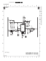
Mono Carrier: Deflection
1
2
A2
3
L03.6L CA
4
7.
17
5
6
7
8
DEFLECTION
Line Deflection
A
Hflybk
3422
I425
A4
46V4
0V0
-12V
100R
2420
820p
13n
EHT
F424
FOCUS
F426
100n
100n
TO PICTURE TUBE
F427
F425
2421
3426
220n
2429
RES
2471
B
LOT
5441
1142.5093D
7421
BUT11APX
I426
3424
* 2424
0V3
* 2423
6422
BY268
470K
F428
TO CRT PANEL
VG2
47R
9
10
Item
14LPD
20LPD
14SDI
20SDI
3456
3473
3474
2423
2424
2441
3403
3404
3441
3442
3443
3444
3447
3451
3455
4R7
4R7
12N
820P
22N
470R
47K
150K
3R3
2R2
220K
680R
470R
47K
3R3
3R9
15N
820P
15N
1K
1K
56K
100K
3R3
2R2
100K
1K8
2K2
4R7
4R7
12N
330P
22N
470R
47K
150K
1R5
1R5
220K
3460
6448
100K
-
47K
-
100K
-
47K
3R3
3R9
15N
15N
1K
1K
56K
100K
0R47
0R47
100K
1K8
2K2
47K
680R
470R
11
A2
A
B
EGP20DL
10
10
1R0 F464
120K
137V0
3410
7440
BF423 3V5
RES
6452
A4
EHT
A1
*
6451
I451
I450
2455
3R3
3440
33K
3439
2M2
150K
BZX79-C33 3457
6453
3459
F443
* 3455
Beam_Limit
A4
2K2
BAS316
MainSupplyGND
* 3460
BAS316 I452
100K
FILAMENT
A4
F446
3445
1R0
Frame Deflection
160VD
TO 1300
OF CRT PANEL
470u
2448
2446
F449
RGP10D
7464
BD135
I438
0V0
I432
2464
7462
BC857B
VDrive+
7465
BD136
0V0
7463
Frame_OUT
15n
A4
10K
1402
F461
-12V5
VERTICAL
DEFLECTION
COIL
1
2
Frame_FB
G
B2P-VH
MULTIPLE BOARD 11 NC : 3139_123_6168
SINGLE BOARD 11 NC : 3139_123_6169
3464
3R3
*
3R3
* 3473
3474
2K2
I434
H
FUNCTION 11NC : 8239_125_1241
CELL 11NC
: 8239_125_1236
G_16560_013.eps
210706
3139 123 6169.2
1
F
8K2
F462
BC546B
-12V5
-12V
E
0V0
-12V0
I436
1K0
2470
I440
1464 OF
1465 OF
3476
I443
470p
3466
3465
0V0
0V0
1R0
3
-11V9
3
-12V6
BAS316
6464
1
1K0
A4
I439
0V9
3478
1M0
3462
1
7461
BC857B
3471
2
0V8
-12V
220R
1V4
2
3472
2
1
2
3
1465 TO
1464 TO
RGP10D
3475
220R
2K2
3461
1
7466
BC847B
1400
WH03D-1
68n
6461
RGP10D
I442
6425
1
BAS316
2R2
2
BAS316 6424
-0V5
3470
A4
100u 50V
BAS316
2463
1n0
6460
2462
2K2
3463
1n0
2461
330R
I455
I456
2460
I444
10u
3468
2465
I437
6462
I441
23V8
160V
A2
G
I454
I453
FILAMENT
VDrive-
F450 1463
6463
D
-12V
F448
3448
C
22n 2441
1R0
2457
1R0
3446
EHTO
68K
140V0
I449
470u
2K2
3402
6444
6446
RGP10D
6447
33u
5401
33K I448
VTSupply
470p
E
H
* 3447
9403 RES
EGP20D
RGP10D
5402
9402 RES
47u
2405
I431
I445
22u
*
1R0
F
6448
* 3444
1K0
33K
3450
*
F463
5
5
3403
F422
I446
2444
1K0
* 3442
* 3443
560n
*
6421
BAS316 3441
4
F404
BAV21WS-V
1K0
D
2
120K
4401
I447
100K
3
4
3405
3449
8K2
9
* 3451
9
10u 16V
6
7
2
6V0
2408
2428
7
3404
MainSupply
6
3
I430
330R
8
10u 250V
2447
5V6
8
470p
6445
1R0
1K0
1K0
3432
3430
BC807-25
1
-7V0 I428
PSD10-204B
1
F406
F405
5
470n
BAS316
Vaudio
3425
1
4
7423
1R0
3423
1
1401
B2P(4-2.3)-VH
6
47u
FILAMENT
A2
5421
F407
2473
I424
6423
3
3V4
HORIZONTAL
DEFLECTION
COIL
*
F429
100n
3421
C
3428
7422
BC817-25
2406
A4
0V0
0V0
220R
6426
2427
HDRIVE
BAS316
1n0
2426
I427
2
3
4
5
6
7
8
9
10
11
1400 E10
1401 C4
1402 G6
1463 E8
1464 E11
1465 E11
2405 D3
2406 D4
2408 D5
2420 B2
2421 B3
2423 A4
2424 A4
2426 B2
2427 B1
2428 D2
2429 B2
2441 C9
2444 E8
2446 E8
2447 E8
2448 E8
2455 D9
2457 E7
2460 E6
2461 F2
2462 F3
2463 F3
2464 F3
2465 F5
2470 F5
2471 B1
2473 C7
3402 D5
3403 D4
3404 D4
3405 D4
3410 C9
3421 C2
3422 A3
3423 C2
3424 B1
3425 C1
3426 B3
3428 B3
3430 C2
3432 C2
3439 D8
3440 D8
3441 C8
3442 D8
3443 D7
3444 D7
3445 D7
3446 E6
3447 C8
3448 E7
3449 C8
3450 C9
3451 C9
3455 C10
3457 C8
3459 D8
3460 D9
3461 F1
3462 G2
3463 F2
3464 G3
3465 G2
3466 G3
3468 F4
3470 F4
3471 F5
3472 G5
3473 H5
3474 H5
3475 F6
3476 F6
3478 G5
4401 D4
5401 E5
5402 E4
5421 C3
5441 B5
6421 D4
6422 A4
6423 C1
6424 F2
6425 F3
6426 B2
6444 D7
6445 C7
6446 D7
6447 D7
6448 D7
6451 C9
6452 D9
6453 D8
6460 F3
6461 F6
6462 E5
6463 E6
6464 F4
7421 B3
7422 B2
7423 C3
7440 C8
7461 F2
7462 F3
7463 G4
7464 E4
7465 G5
7466 F4
9402 E4
9403 C9
F404 D5
F405 C5
F406 C5
F407 C5
F422 D2
F424 B2
F425 B3
F426 B3
F427 B4
F428 B4
F429 C2
F443 C10
F446 D9
F448 D9
F449 E9
F450 E8
F461 G6
F462 G6
F463 D6
F464 D7
I424 C2
I425 A2
I426 B2
I427 B3
I428 C3
I430 C2
I431 D4
I432 F1
I434 G2
I436 G3
I437 E3
I438 E4
I439 F4
I440 F4
I441 E5
I442 F5
I443 F5
I444 E6
I445 C8
I446 C8
I447 C8
I448 C9
I449 C9
I450 C9
I451 C9
I452 D9
I453 E10
I454 E10
I455 E10
I456 E10
Circuit Diagrams and PWB Layouts
L03.6L CA
7.
18
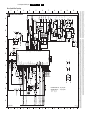
Mono Carrier: Tuner IF
1
A3
2
3
4
5
6
7
8
TUNER IF
A3
A
A
+5V
VTSupply
3005
RES
9003
F001
5003
TUNER_AGC
RES
B
F005
A4
100R
VTSupply_A
+5V
100u
2002
22K
2
3
C
4
1003
3003
5
SDA
VTS
100R
10u
1001
OFWG1984M
TU
AS
TUNER
SCL
IF
11
F003
1
2
SDA
3
GND
10
12
13
NC
14
15
6
I
IGND
O1
O2
5
4
VIF_1
VIF_2
C
A4
A4
GND
F004
38M9
8
22p
B3B-EH-A
220n
9
6001
2005
7
VS
100R
22p
2004
SCL
3004
2003
A4
A4
1
2
3
1
AGC
5001
3002
10n
1000
UV1336
2001
470u 10V
2006
4K7
BZX79-C33
2007
3001
820n
B
5002
F006
I001
D
1004
D
TO 1520 OF
E
E
F
F
FUNCTION 11NC : 8239_125_0987
CELL 11NC
: 8239_125_0980
MULTIPLE BOARD 11 NC : 3139_123_6168
SINGLE CHASSIS 11 NC : 3139_123_6169
G_16560_014.eps
210706
3139 123 6169.2
1
2
3
4
5
6
7
8
1000 C4
1001 C7
1003 C2
1004 D5
2001 C2
2002 C3
2003 D4
2004 D4
2005 C6
2006 C2
2007 C6
3001 B3
3002 C3
3003 C3
3004 C3
3005 B2
5001 C6
5002 B5
5003 B5
6001 C6
9003 B5
F001 B2
F003 C6
F004 C6
F005 B6
F006 B5
I001 D5
470u
+3V3
100R
4K7
3641
3497 390R
SCL
ADR
1
2
SDA
7
2642 F641
3V3
6
3V3
5
3V3
4
2
F643
SCL
A4
2499
LED
34 0V8
33 1V0
10
11
22 1V3
21 1V3
3647
2K7 100p
4 0V8
2v8 3619
2v5 3620
2v6 3621
51
52
53
C
SDA
A4
FBISO
A
B
VDR
HOUT
5
6
P0
RO
GO
BO
IFVO
SVO
IR
IR
VSSC|P
GND
VSSA
+3V3A
+3V3A
DECBG
RESET
0V 60
4V0 19
DECDIG
5499
4662 RES
470n
2601
2u2
2498
4u7
2483
100n
2484
100n
100n
50R
5605
50R
5561
F
3602
+3V3
3601
5u6
+3V3
+3V3
3618
+5V
5604
33K
10K
MULTIPLE BOARD 11NC : 3139_123_6168
SINGLE BOARD 11NC
: 3139_123_6169
3487
3489
1n0
G
EHTO
SCL
SDA
9410
+8VD
FUNCTION 11NC : 8239_125_1242
CELL 11NC
: 8239_125_1237
H
A2
A1
A7
A7
A3,A5
A3,A5
Std_Con
IR
KEYBOARD
F441
2615
BAS316
Beam_Limit
A2
E
5497
2K2
2K2
2489
2488
3604
3605
F204
2K2
5V0 15
VSC
3V8 26
100R 3V3 2
100R 3V3 3
2V0 36
EHTO
P1<0:3>
INT1
T0
INT0
T1
P1<6,7>
SCL
SDA
0V F202
18 0V
30 0V
41
0V
12
F601
1K0
A2
A7
9
27u
H
A3
A3
0V
50R
I612
1203
Frame_OUT F624
SY_CVBS_IN
BAS316
A4
A4
A4
3624
F648
To 1300
of CRT PANEL
VIF_1
VIF_2
6681
RED
GREEN
BLUE
F606
BLK_IN
470R
3209
1
2
3
4
5
6624
2209
220n
470R
62
63
64
1
I618
100R
3607
10u 16V
2201
4n7
2202
820p
3210
75R
3211
2n2
2487
1M0
3483
I606
3V4
0V2
0V2
3V4
5
6
7
3V3 8
F607
1K0
1622
3208
0
1
ADC
2
3
PWM<0:3>
P3<0:3>
BCL
IN
BLK
3v4 49
5v3 50
2V7 47
2V6 46
2V7 48
INSSW2
VIN
R2
YIN
G2
UIN
B2
I611 0V0 45
+8V
2616
I601
560R
3201
3232
3231
I602
2490
2210
100R
1202
REFO 1
4u7
0V 20
5v0 32
SNDPLL
SIFAGC
AUDEEM
AVL
REF0
SNDIF
DECSDEM
AVL
EWD
2V4 31
1V5 43
CVBS1
CVBS
Y
C
PLLIF
2V9 37
I605
3v9 40
220n 3V3 42
3207
I604
100n
I610
G_16560_015.eps
210706
3139 123 6169.2
1
2641
1n0
WC
B
3642
100R
(2Kx8)
EEPROM
0 NVM
100R
2
3
3V4
Φ
3643
1K0
3634
GND
3
OUT
3644
F494
OUT
COM
1
22u 25V
IN
2492
1
IN
1N 6491
3V3 BAV70
8
7641
M24C16-WBN6
10R
10R
3479
3493
7493
LE33CZ-AP
220u 25V
3K3
2494
3492
10K
BZX384-C5V6
A2
A1
10R
6492
5V0
7494
BC337-25
4V1
680R
2481
100p
33R
2493
3V3
+8V
FILAMENT
F493
4491
F492
3494
9V0
3495
I617
7491
BC847B
9V6
3498
+5V
+3V3
+3V3A
+8V
VTSupply_A
56K
I616
11V5
I609
3496
5V6
3491
6481
BAS316
F481
3K3
100R
3490
3488
1n0
2497
1K0
1K0
1n0
2496
3485
I614
6V5
A
F642
2K7
2207
2486
4n7
1u0
390R
1
IFIN
2
IREF
2205
18K
I607
2485
3480
10u
4n7
2206
3481
I608
F
33p
2602
12M
1621
3646
2643
2603
1V8 23
1V8 24
39K 3V9 25
17
16
3V8
3V0
VPE
AUDEEM
1
SIFIN
2
DECSDEM
1
PHLF
2
28
29
2V3 55
33p
G
470u 10V
9476 RES
D
3V2
2V3
1V6 59
1V6 58
0V 57
100n
2605
+3V3
1u0
2608
2482 1u0
39
3V3
54
1M0
220p
2491
470u 10V
E
5601
VDDA VP1 VP2
14
8v2
XTALIN
8v3
10u
F491
2495
F644
P2.0
TPWM
3V3
56
AGCOUT
5u6
AUDOUT
5602
AUDEXT
QSSO
3V3
61
5u6
Vaudio
A2
HDRIVE
Hflybk
A2
A2
A2
VDrive+
2604
2u2 10V
2692
2K2
10K
3606
3603
0V4
I613
10u 16V
+3V3
VDrive-
1K0
8V3
4661
RES
3645
7601
PDTA114ET
8V3
F208
F645
F646
F647
2208
44
35 3V8
38 2V4
3V3
1K0
1u0
3206
220n
2123
2212
13 2V3
5u6
5482
7496
BD135
8V3
11
1n0
IC
100n
5603
+8VD
+8V
10
7200
TDA9370PS/N3/A
VDDC VDDP
100n
2606
2607
GND
9
9V8
3499
27K
+3V3
I619
BAS316
BAS316
BAS316
8
+8V
Φ
+3V3
3205
2
O
TV SIGNAL
PROCESSOR
OSCGND
CLOSED CAPTION
DECODER
XTALOUT
& EMBEDDED uC
C
3
O
6628
6627
6626
270R
1
I615
7
470R
470R
470R
75R
3V3
2612
220u 16V
100n
4u7
1201
TPSRA
4M5
I
2V7
1K0
3204
3203
5201
7202
BC847B
4606
RES
3V3
27 4V2
100n
7201
I603
I
TUNER_AGC
+8V
470u 10V
7V0
100R
BC847B
D
8V3
2204
3202
2203
+8VD
6625
BZX79-C8V2
9200
2V7
F201
6
VOLUME
A5
A5/A7
L1_IN
B
5
AM_FM_MONO
A
19
A6
4
VIDEO PROCESSING
A4
7.
A3
A4
A4
A4
3
RED
GREEN
BLUE
Mono Carrier: Video Processing
1
2
L03.6L CA
3486
Circuit Diagrams and PWB Layouts
2
3
4
5
6
7
8
9
10
11
1201 C1
1202 F4
1203 G5
1621 F2
1622 G4
2123 C3
2201 F4
2202 F4
2203 B2
2204 B4
2205 F3
2206 F2
2207 F3
2208 C4
2209 G2
2210 F3
2212 C3
2481 B7
2482 E1
2483 F7
2484 F7
2485 F2
2486 F3
2487 G3
2488 F6
2489 F6
2490 F4
2491 E1
2492 C9
2493 B9
2494 B7
2495 A10
2496 C6
2497 C6
2498 F7
2499 C5
2601 F7
2602 F2
2603 F2
2604 B6
2605 E2
2606 D1
2607 D1
2608 E1
2612 B5
2615 G5
2616 F5
2641 B11
2642 C10
2643 F1
2692 B6
3201 F4
3202 B2
3203 C4
3204 C2
3205 C2
3206 C4
3207 F3
3208 G2
3209 G2
3210 F3
3211 G3
3231 F4
3232 E5
3479 B8
3480 F3
3481 F2
3483 G2
3485 C6
3486 C6
3487 G6
3488 C6
3489 G6
3490 C6
3491 B7
3492 B7
3493 B8
3494 B9
3495 B9
3496 A10
3497 A10
3498 C7
3499 B7
3601 F6
3602 F6
3603 B5
3604 F6
3605 F6
3606 B6
3607 F5
3618 F6
3619 C4
3620 C4
3621 C4
3624 G5
3634 C8
3641 B11
3642 C11
3643 C11
3644 B11
3645 B5
3646 F1
3647 C5
4491 B9
4606 B4
4661 A5
4662 F7
5201 C2
5482 E1
5497 E10
5499 E10
5561 F10
5601 E1
5602 D1
5603 D1
5604 F10
5605 F10
6481 B7
6491 B9
6492 B10
6624 G5
6625 A5
6626 C5
6627 C5
6628 C5
6681 G5
7200 D2
7201 B2
7202 B4
7491 B7
7493 B9
7494 B10
7496 A8
7601 B5
7641 B10
9200 B4
9410 H6
9476 A10
F201 B2
F202 D7
F204 F6
F208 C4
F441 G6
F481 B7
F491 A8
F492 B9
F493 A9
F494 A9
F601 E7
F606 G4
F607 F5
F624 H5
F641 C10
F642 C11
F643 C11
F644 C9
F645 C4
F646 C4
F647 C4
F648 G4
I601 F4
I602 F4
I603 C3
I604 F3
I605 E3
I606 G2
I607 F2
I608 F3
I609 B7
I610 F2
I611 E4
I612 G5
I613 B5
I614 B5
I615 A5
I616 B8
I617 B7
I618 E6
I619 B5
Circuit Diagrams and PWB Layouts
L03.6L CA
7.
20
Mono Carrier: Audio - BTSC Stereo Decoder
1
A5
2
3
4
5
6
7
8
9
10
AUDIO - BTSC STEREO DECODER (ECONOMIC)
A5
A
A
B
B
2891
R1_IN
A7
100n
4863
3867
COMP
I866
3n3
150p
2u2
2873
23
AUTOMATIC
VOLUME AND
LEVEL CONTROL
INPUT
SELECT
24
21
20
BCR 4V1
44
VIR 4V1
0V0
34
VAR 4V1
29
0V0
22
NC
0V0
17
CAV 6V7
0V0
12
NC
26
0V0
LIR 4V
LOR 4V1
CSS 4V1
0V
4u7
2876
2u2
2u2
2864
NC
25
19
VOLUME
RIGHT
CTRL
TONE OUTR 18 4V1
RIGHT
CTRL
VOLUME
LEFT
CTRL
TONE
LEFT
CTRL
10
13
14
4V1 BCL
11
4V1 TC2L
37
4V1 TC1L
38
4V1 VIL
39
4V1 VAL
40
0V0 DGND
7
3V3 SDA
3V3 SCL
Main_OutR
A6
I871
Main_OutL
OUTL 16 4V1
A6
D
15
2869
2868
4852
3n3
150p
2867
2u2
2866
RES
2881
RES
2882
100K
68n
RES
8
LOGIC
I2C
TRANSC
0V0 MAD
1V1 RFR
9
4V1 LIL
36
4V1 LOL
0V0 AGND
F861
27
3861
4n7
2879
22n
E
4V1 VREF
100u I870
2874
8V1 VCAP
I869
I868
28
100u
41
2875
30
8V2 VCC
31
4V1 TW
32
FIL
AND
REF
SUPPLY
10u
4V1 BPU
1K2
FDO
4V1 CW
DET AND
VOLTAGE
CTRL AMP
4V1 33
100R
3863
3864
L-R
6
DEMATRIX
+ MODE
SELECT
2877
15K
2880
CER 6V6
4V1 35
L+R
1
C
68n
FDI
I867
D
STEREO DECODER
5
1u0
RES
2863
3862
43
2870
I865
TC2R 4V1
4V1 4
2u2
42
I863
2878
A4
3
CPH 4V1
2862
AM_FM_MONO
2
CP1 4V1
7861
TDA9853H
CP2 4V1
220n
CMO 4V1
C
1861
2861
CSBLA 514K5
I862
220n
2865
3K3
2885
2871
2u2
RES
2872
I861
TC1R 4V1
2884
E
5861
+8V
2883
470u
4861
10u
RES
4865
1883
1
2886
L1_IN
A7
100n
3866
SCL
F
A4
SDA
A4
G
100R
5862
3865
10u
F
100R
FUNCTION 11NC : 8239_125_1245
CELL 11NC
: 8239_125_1238
G
MULTIPLE BOARD 11NC : 3139_123_6168
SINGLE CHASSIS 11NC : 3139_123_6169
G_16560_016.eps
210706
3139 123 6169.2
1
2
3
4
5
6
7
8
9
10
1861 C5
1883 F4
2861 C5
2862 C2
2863 D3
2864 C5
2865 C5
2866 E7
2867 E7
2868 E8
2869 D8
2870 C8
2871 C8
2872 C7
2873 C7
2874 E5
2875 E5
2876 C6
2877 E5
2878 E5
2879 E5
2880 E3
2881 E7
2882 E6
2883 E4
2884 B4
2885 C4
2886 F2
2891 B2
3861 E6
3862 D4
3863 D3
3864 D3
3865 F4
3866 F4
3867 B5
4852 E8
4861 E8
4863 B8
4865 F8
5861 E4
5862 F9
7861 C4
F861 D5
I861 B4
I862 C5
I863 C5
I865 C6
I866 D4
I867 D3
I868 E3
I869 D5
I870 D5
I871 D6
Circuit Diagrams and PWB Layouts
L03.6L CA
Mono Carrier: Audio Amplifier + Mono Sound Processing
1
2
3
4
A6
7.
21
5
6
7
8
9
10
11
AUDIO AMPLIFIER + MONO SOUND PROCESSING
A6
A
A
AmpOutR+
5
1
B
CH1+ 2 5V1
1V4 6 CH1-IN
AmpOutL_Neg
820p
CH2- 10 5V1
I905
0V4 9 VOL
VOLUME
820p
3906
3911
100p
100p
2950
2947
C
STEREO OUTPUT
11
100K
1V4
7902
AN7523N
6
7
F914
0V4
10u
3K3
2909
3907
3V8
13V5
*
F913
A4
7
F912
4922
1N4148
10u 16V
3
I901
6909
D
BZX384-C2V7
6908
2908
FILAMENT
2952
1u0
15K
5
4
3
2
1
AmpOutR_Neg
CH2+ 12 5V1
GNDCH2
2906
I902
GNDINP
3905
F903
1n0
Main_OutR
A5
2907
C
GNDCH1
4925
RES
F911
9874 RES
AmpOutR_Pos
*
1900
F909
100p
2949
1V4 8 CH2-IN
F906
AmpOutL_Pos
4927
I904
100p
2948
2905
10K
3904
CH1- 4 5V1
680K
3909
2951
1u0
15K
A7
A7
VCC
STB
2904
3903
1n0
F901
Main_OutL
11V4
7901
AN7522N
3V0
1u
3K3
2903
3902
*
4923
RES
A5
A7
AmpOutR_Pos
1K0
B
A7
AmpOutL_Pos
3901
4924
+5V
AmpOutL+
RES
2901
RES
4921
Vaudio
9
5
1
VCC
CH_IN
9865
CH_OUT+
GND
GND
VOLUME
CH_OUT-
STANDBY
NC
D
5V1
2
9872
3
5V1
4
8
MONO OUTPUT
E
E
F
Item
Mono
Stereo
7901
7902
1900
AN7523
3 PIN
AN7522
5 PIN
MULTIPLE BOARD 11NC : 3139_123_6168
SINGLE CHASSIS 11NC : 3139_123_6169
F
FUNCTION 11NC : 8239_125_1244
CELL 11NC
: 8239_125_1238
G_16560_017.eps
210706
3139 123 6169.2
1
2
3
4
5
6
7
8
9
10
11
1900 B10
2901 A7
2903 B5
2904 B5
2905 B5
2906 C5
2907 C5
2908 C3
2909 E4
2947 C9
2948 C9
2949 C9
2950 C10
2951 B5
2952 C5
3901 B5
3902 B5
3903 B3
3904 B4
3905 C3
3906 C4
3907 E4
3909 C4
3911 C3
4921 A4
4922 C8
4923 B3
4924 B3
4925 C3
4927 B9
6908 D3
6909 D3
7901 B6
7902 D6
9865 D8
9872 D8
9874 C9
F901 B2
F903 C2
F906 B10
F909 B10
F911 C10
F912 C10
F913 D3
F914 D2
I901 D3
I902 C4
I904 B9
I905 C8
Circuit Diagrams and PWB Layouts
Mono Carrier: Front I/O + Front Control + Headphone
1
2
3
A7
L03.6L CA
7.
4
5
22
6
7
8
9
FRONT IO + FRONT CONTROL + HEADPHONE
A7
A
A
FRONT CINCH
1
2
3
5
6
4
L1_IN
4183
RES
47K
3184
330p
*
TS
*3185
I183
R1_IN
1K0
3681
3682
channel-
0R
1603
1602
F683
USA
I685
volume+
volume-
1601
1600
*
47K
3186
330p
F693 6695
100R
100R
3693
LTL-10224WHCR
3694
3696
D
3697
I687
2
HEADPHONE
3
F986
1982
120R
A4
OUT
E
F
120R
F988
1981
100u
4694
F983
470p
3981
2982
2981
4982
RES
4981
RES
A6
VS
For Engg purposes only
F987
AmpOutL+
1
1901
2
4
5
6
RES
9982
F
2984
100u
F692
1
9
8
7
3
F985
3982
I982
470p
2983
AmpOutR+
A6
AmpOutR_Pos
9694
6692
TSOP1836UH1
GND
HEADPHONE
SOCKET
4984
RES
4983
RES
F984
F691
IR
A6
220R
3695
100u
I686
100R
LED
+3V3A
RES
4697
2691
*
2183
RES
RES
4695
D
G
F982
AmpOutL_Pos
A6
G
Mono
MULTIPLE BOARD 11 NC : 3139_123_6168
SINGLE BOARD 11 NC : 3139_123_6169
H
H
FUNCTION 11NC : 8239_125_1246
CELL 11NC
: 8239_125_1239
G_16560_018.eps
210706
3139 123 6169.2
1
C
F684
A5
150R
2186
1101-3
Stereo
2K2
1606
4K7
F183
8
9
7
1183
R
Item
3687
channel+
B3B-EH-A
RED
E
3688
3686
430R
3685
200R
I684
POWER
1
2
3
F185
B
A5,A4
1103
2182
RES
2185
150R
200R
I182
3183
RES
3689
F182
1182
1101-2
*
I683
I682
L
5
6
1100-2 4
RED
3683
RES
4182
22p
75R
A4
*
WHITE
C
F682
A4
BZX79-C6V8
*
6181
F184
100R
3181
1101-1
1181
V
2
3
1100-1 1
WHITE
2
3
1
KEYBOARD
SY_CVBS_IN
B3B-EH-A
3182
120R
F181
YELLOW
2181
MONO SET
B
FRONT CONTROL
1102
2
3
4
5
6
7
8
9
1100-1 B1
1100-2 C1
1101-1 B2
1101-2 C2
1101-3 D2
1102 B5
1103 C5
1181 B2
1182 C2
1183 D2
1600 C9
1601 C9
1602 C9
1603 C8
1606 C7
1901 E5
1981 G3
1982 F3
2181 B3
2182 C3
2183 D3
2185 C2
2186 D2
2691 E9
2981 F2
2982 G3
2983 F2
2984 F3
3181 B2
3182 B3
3183 C3
3184 C3
3185 C3
3186 D3
3681 B9
3682 C9
3683 B7
3685 B8
3686 B9
3687 B9
3688 B9
3689 C7
3693 D9
3694 E8
3695 D7
3696 D7
3697 D8
3981 F3
3982 F3
4182 B7
4183 C4
4694 F7
4695 D7
4697 D8
4981 G2
4982 G2
4983 E2
4984 E2
6181 B3
6692 E9
6695 D8
9694 E8
9982 F2
F181 B3
F182 C3
F183 C3
F184 B2
F185 C2
F682 B7
F683 C9
F684 C7
F691 E7
F692 E8
F693 D7
F982 G5
F983 F3
F984 E5
F985 F3
F986 E4
F987 F7
F988 F7
I182 C3
I183 C3
I682 B7
I683 B8
I684 B8
I685 C9
I686 D7
I687 E9
I982 F3
Circuit Diagrams and PWB Layouts
L03.6L CA
7.
23
Layout Mono Carrier (Top Side)
1000
1001
1003
1004
1100
1101
1102
1103
D4
C4
D4
C4
A4
A4
A3
A3
1201
1202
1203
1400
1401
1402
1463
1464
B4
C4
A3
C3
D3
D3
D3
C3
1465
1500
1501
1511
1512
1515
1520
1531
B2
A1
A1
A1
B2
A2
B2
A1
D
1600
1601
1602
1603
1606
1621
1622
1861
A3
A3
A2
A2
A1
B3
B3
A3
1883
1900
1901
2002
2006
2007
2204
2205
A3
A4
A4
D4
D4
D4
B4
C4
2405
2406
2408
2423
2424
2428
2441
2444
C2
D2
D2
D3
C2
D3
D2
D2
2446
2447
2448
2455
2457
2460
2463
2465
D3
D2
C3
C3
D2
C1
D3
D3
2470
2488
2491
2492
2493
2494
2495
2498
D4
C4
C4
B3
A4
B3
A4
C4
2500
2501
2502
2503
2505
2507
2515
2523
A1
A1
A1
B1
B2
B1
B2
B1
C
2525
2560
2561
2562
2564
2580
2612
2616
B1
B2
B2
B2
C2
A2
A3
B4
2691
2692
2864
2865
2869
2870
2874
2875
A2
A3
A4
A4
A4
A4
A3
A3
2876
2877
2878
2883
2884
2885
2903
2908
A3
A3
A3
A3
A3
A3
A4
A4
2909
2981
2983
3005
3181
3182
3183
3185
A4
A4
A4
C4
A4
A4
A3
A3
3204
3205
3208
3210
3402
3403
3404
3405
B4
B4
B4
B4
D2
D2
D2
C2
3410
3421
3422
3423
3424
3425
3426
3428
B
C3
D4
C2
D3
D3
B2
C2
D3
3439
3442
3443
3444
3445
3446
3448
3449
C2
C3
D3
D3
D2
C1
D2
C3
3450
3459
3464
3468
3470
3471
3472
3473
C3
C3
D3
D3
D3
D3
D3
D3
3474
3475
3478
3479
3485
3486
3488
3491
D3
C3
D4
B3
C4
C4
B4
C4
3493
3494
3495
3496
3497
3498
3500
3501
A3
A3
A4
B4
A4
B4
A2
A2
3502
3503
3505
3507
3508
3509
3510
3523
A1
A2
A1
B1
A1
A2
A2
C1
3524
3526
3527
3528
3543
3549
3581
3604
C1
B1
B1
B1
C2
C2
B1
B3
3605
3618
3619
3620
3621
3624
3634
3693
B3
B3
B4
B3
B3
B4
A3
A2
3865
3866
3901
3982
5001
5002
5003
5201
A3
A3
A4
A4
C4
D4
C4
A4
5401
5402
5421
5441
5482
5497
5499
5500
D2
D2
D3
D1
B4
A2
A3
A2
5501
5509
5515
5520
5560
5561
5562
5563
A2
B2
B1
C2
B2
B2
B2
C2
5601
5602
5603
5604
5605
5861
5862
6001
B3
B3
B3
B2
A4
A3
A3
D4
6181
6422
6444
6446
6447
6448
6453
6461
A4
D3
D2
D1
D2
D3
C3
D1
6462
6463
6500
6501
6502
6503
6521
6560
D1
D1
A1
A1
A1
A1
C1
B2
6562
6581
6625
6692
6695
6909
7200
7421
B2
B1
B3
A2
A1
A4
B4
C3
A
1
1
2
2
3
3
4
4
G_16560_019.eps
210706
3139 123 6169.2
D
C
B
A
7440
7463
7464
7465
7493
7494
7496
7515
7520
7641
7901
7902
9001
9002
9003
9005
9200
9203
9402
9403
9404
9405
9406
9407
9408
9410
9411
9412
9421
9422
9424
9441
9444
9445
9446
9448
9449
9452
9463
9464
9465
9471
9473
9475
9476
9478
9479
9481
9490
9494
9495
9496
9497
9498
9499
9500
9501
9509
9522
9523
9539
9560
9561
9562
9564
9569
9582
9604
9605
9606
9607
9608
9612
9617
9618
9624
9625
9629
9641
9642
9643
9663
9665
9681
9682
9693
9694
9695
9862
9865
9872
9874
9875
9883
9901
9902
9903
9904
9905
9906
9907
9982
9983
C3
C3
D3
D3
A3
A4
B3
C1
B1
B3
A4
A4
D4
C4
C4
C4
B4
A4
D2
C3
D3
C2
C2
C3
C3
C3
C3
C3
D2
C2
D2
C2
D2
C3
D3
C3
C3
C3
C3
C3
A3
D3
D3
C3
B4
D4
D4
B4
A3
A3
A4
A4
A3
A3
A3
A1
A1
B2
C2
B1
C3
B2
A2
B2
B2
A2
C2
B3
B3
B3
A4
B2
A3
B3
B3
B3
B3
B2
B3
B3
B3
B3
B3
B4
A3
A2
A2
A3
A3
A4
A3
A4
A3
A3
A4
A4
A4
A4
A4
A3
A3
A4
A3
Circuit Diagrams and PWB Layouts
L03.6L CA
7.
24
Layout Mono Carrier (Bottom Side)
D
C
B
A
4
3
3
2
2
1
1
G_16560_020.eps
210706
3139 123 6169.2
D
C
B
A
Circuit Diagrams and PWB Layouts
CRT Panel
1
2
3
L03.6L CA
4
7.
5
25
6
7
8
9
10
11
12
CRT PANEL
B1
B1
170V0
170V0
A
68R
3313
A
1303
RES
I313
GREEN
RES
RED
109V0
I302
3302
5
7314
BF423
BF422
33K
180p
3304
7315
F304
GND_CRT
7310
8
I304
6316
104V0
BF422
F306
I305
3306
GND_CRT1
R
I314
106V0
3301
BAS321
9
122V0
1
2V6
4301
P5
P6
I308
D
168V7
P9
3310
120V0
6317
109V0
I316
3309
123V0
1
1K5
5
6
11
7318
BF423
BF422
8
180p
9
3318
220R
2302
3311
220R
7V7
6V3
Heater
CG
10
Heater
CR
H1
CRT
9 Pin
12 Pin
H2
GND
VG1
Pin 1
Pin 6
Pin 1 & 12
Pin 5
Green
Pin 9
Pin 6
VG2
Red
Pin 8
Pin 7
Pin 7
Pin 8
Heater
Heater
Pin 5
Pin 4
Pin 9
Pin 10
Blue
Pin 3
Pin 11
CB
I311
6318
220R
1n0
3320
4307 RES
170V0
GND
1K5
BAS316
3319
BAS316
12
*
6301
2318
GND_CRT
6307
BZX384-C8V2
E
GND_CRT1
GND_CRT1
2303
TO CRT SOCKET
E
1305
EHT
FOCUS
I312
GND_CRT1
47n
2304
VG1 VG2
GND_CRT GND_CRT GND_CRT
680p
F
D
G1
G2
I309 2V7
3V0
7311
RES
Ground
G3
7
418V0
4302
3V0
Red
1K5
7312
220R
GND_CRT
C
Red
1302-A
108V0
3V3
Green
Green
P1
B
BAS321
I307
3305
33K
6V3
I315
CRT
P8
G
7V7
7317
BF422
180p
3308
3V0
Blue
Blue
P7
1K5
170V0
I306
3V0
7309
RES
2301
GND_CRT
B
P4
220R
Filament
D?
TYPE
P3
7316
BF423
3V2
220R
F307
6
7
I317
4308
F305
B8B-EH-A
7V7
168V7
6V3
3307
C
F311
170V0
I303
3V0
7307
RES
3V0
2300
1
2
3
4
5
6
7
8
4
2V6
4300
3303
F303
GND_CRT
3
BAS321
7308
BF422
220R
TO 1622 OF
F302
1300
3V1
220R
4303
*4304
* 4305
** 4306
F301
I301
1301-1
6313
107V6
TO CRT SOCKET
RES
B
1304
Aquadag
168V8
7313
BF422
33K
RES
3300
AND 1400 OF
BLUE
F
FROM MAIN CHASSIS TO LOT
GND_CRT
G
G
Item
14V
20v
3319
4303
4304
JUMP
NO
JUMP
JUMP
JUMP
NO
4305
4306
JUMP
NO
NO
JUMP
L06SP CRT MULTIPLE BOARD 11NC : 3139_123_6172
L06SP CRT SINGLE BOARD 11NC
: 3139_123_6173
H
H
G_16560_021.eps
210706
3139 123 6173.1
1
2
3
4
5
6
7
8
9
10
11
12
D? B9
1300 B1
1301-1 B7
1302-A D7
1303 A7
1304 A8
1305 F10
2300 C4
2301 D4
2302 E5
2303 F3
2304 F2
2318 E5
3300 A4
3301 C6
3302 B3
3303 C4
3304 C4
3305 C6
3306 C3
3307 D4
3308 D5
3309 D6
3310 D3
3311 E4
3313 A5
3318 E5
3319 E6
3320 E5
4300 B3
4301 C3
4302 D3
4303 B2
4304 B2
4305 B2
4306 B2
4307 E3
4308 C2
6301 E4
6307 E3
6313 B5
6316 C5
6317 D5
6318 E5
7307 B3
7308 B4
7309 C3
7310 C4
7311 D3
7312 D5
7313 A4
7314 B4
7315 B4
7316 C4
7317 C5
7318 D5
F301 B2
F302 B2
F303 B2
F304 C2
F305 C2
F306 C2
F307 C2
F311 C2
I301 B3
I302 B4
I303 B4
I304 C4
I305 C3
I306 C4
I307 D3
I308 D4
I309 D4
I311 E4
I312 F5
I313 A5
I314 C5
I315 C6
I316 D6
I317 E7
Circuit Diagrams and PWB Layouts
L03.6L CA
7.
26
Layout CRT Panel (Top Side)
Layout CRT Panel (Bottom Side)
1300
1301
1302
1303
1304
1305
2303
2304
3300
3301
3304
3305
3308
3309
3310
3313
3318
3319
7308
7310
7312
7313
7314
7315
7316
7317
7318
9300
9302
9303
9304
9314
9315
9316
9317
9318
3139 123 6173.1
G_16560_022.eps
170706
2300
2301
2302
2318
3302
3303
3306
3307
3311
3320
4300
4301
4302
4303
4304
4305
4306
4307
4308
6301
6307
6313
6316
6317
6318
7307
7309
7311
A1
B1
B1
B1
B1
B1
A1
A1
A1
A1
A1
B1
A1
B1
A1
A1
B1
B1
A1
A1
A1
A1
A1
A1
A1
A1
A1
A1
A1
A1
A1
A1
A1
A1
A1
A1
3139 123 6173.1
G_16560_023.eps
170706
A1
A1
A1
A1
A1
A1
A1
A1
A1
A1
A1
A1
A1
A1
A1
A1
A1
A1
A1
A1
A1
A1
A1
A1
A1
A1
A1
A1
Alignments
L03.6L CA
8.
EN 27
8. Alignments
Index of this chapter:
8.1 General Alignment Conditions
8.2 Hardware Alignments
8.3 Software Alignments and Settings
Note: The Service Default Alignment Mode (SDAM) is
described in the "Service Modes, Error Codes and Fault
Finding" section. SDAM menu navigation is performed by using
the MENU UP, MENU DOWN, MENU LEFT, and MENU
RIGHT keys of the remote control transmitter.
8.1
General Alignment Conditions
Perform all electrical adjustments under the following
conditions:
• AC voltage and frequency: according to country's
standard.
• Connect the television set to the AC power via an isolation
transformer.
• Allow the television set to warm up for approximately 20
minutes.
• Measure the voltages and waveforms in relation to chassis
ground (with the exception of the voltages on the primary
side of the power supply). Never use heatsinks as ground.
• Test probe: Ri > 10 M ohm; Ci < 2.5 pF.
• Use an isolated trimmer/screwdriver to perform the
alignments.
8.2
Hardware Alignments
1531
5500
7520
1
2503
7200
4
A SDAM
9448
5441
B
1000 (TUNER)
LOT
Focus
Screen
VG2
ComPair
J1003
D
G_16560_024.eps
180706
Figure 8-1 Top view mono carrier
8.2.1
Vg2 Adjustment
1. Activate SDAM by pressing the following key sequence on
the remote control transmitter: 0 6 2 5 9 6 directly followed
by the MENU button (do not allow the display to time out
between entries while keying the sequence).
2. Use the MENU UP/DOWN keys to highlight the WHITE
TONE sub menu.
3. Press the MENU LEFT/RIGHT key to enter the WHITE
TONE sub menu.
4. In the WHITE TONE sub menu, press the MENU UP/
DOWN keys to select NORMAL RED, NORMAL GREEN,
or NORMAL BLUE.
5. Use the MENU LEFT/RIGHT keys to set the values of
NORMAL RED, NORMAL GREEN and NORMAL BLUE to
'40'.
6. Press the MENU button twice to enter the normal user
menu.
7. In the normal user menu, use the MENU UP/DOWN keys
to highlight the PICTURE sub menu (if necessary).
8. Press the MENU LEFT/RIGHT keys to enter the PICTURE
sub menu.
9. Use the MENU UP/DOWN keys to select CONTRAST. Be
sure to record the current value of CONTRAST.
10. Use the MENU LEFT/RIGHT keys to set the value of
CONTRAST to '0'.
11. Use the MENU UP/DOWN keys to select BRIGHTNESS.
Be sure to record the current value of BRIGHTNESS.
12. Use the MENU LEFT/RIGHT keys to set the value of
BRIGHTNESS to minimum (OSD just visible in a dark
room).
13. Press the MENU button twice to return to the top level
SDAM menu.
14. Press the OSD/STATUS button to hide the SDAM onscreen display ("S" indication remains visible). This, to
avoid interferences during the waveform measurements
15. Connect the RF output of a video pattern generator to the
antenna input, and input a 'black picture' test pattern to the
television set.
16. Set the oscilloscope to 50 V/div and the time base to 0.2
milliseconds (external triggering on the positive vertical
pulse with a 10:1 probe).
17. Ground the scope at the CRT panel and connect a 100:1
probe to one of the cathodes of the picture tube socket (pin
7= Red, pin 9= Green, and pin 3= Blue, see also schematic
diagram B1). Measure the level of the black current
measuring pulses. These are the second line (Red), third
line (Green), and fourth line (Blue) directly after the frame
blanking (see figure "Vcut-off"). Remark: This chassis is
using a TDA93XX UOC series. These use two different
measuring pulses at each of the R, G, and B outputs. The
above-mentioned level applies to the pulse with the lowest
level of each gun.
18. Select the cathode with the highest VDC value for the
alignment. Adjust the Vcut-off of this gun with the SCREEN
potentiometer (see figure "Top view family board") on the
LOT to the correct value (see table "Vg2 alignment
values").
19. Press the OSD/STATUS button to display the SDAM onscreen display.
20. Press the MENU button to enter the normal user menu.
21. In the normal user menu, use the MENU UP/DOWN keys
to highlight the PICTURE sub menu (if necessary).
22. Press the MENU LEFT/RIGHT keys to enter the PICTURE
sub menu.
23. Use the MENU UP/DOWN keys to select CONTRAST.
24. Use the MENU LEFT/RIGHT keys to reset the value of
CONTRAST to the original value.
25. Use the MENU UP/DOWN keys to select BRIGHTNESS.
26. Use the MENU LEFT/RIGHT keys to reset the value of
BRIGHTNESS to the original value.
27. Press the MENU button twice to return to the top level
SDAM menu.
28. Use the POWER button on the remote control transmitter
or the POWER button on the television set to turn off the
television set. This will save the changes made in SDAM.
EN 28
8.
L03.6L CA
Alignments
max.
VCUTOFF [VDC]
0V Ref.
E_06532_011.eps
110204
Figure 8-2 V_cutoff
Table 8-1 Vg2 alignment values
8.2.2
Screen Size
Cut-off point (V)
14
+135 V ± 4 V
20
+140 V ± 4 V
Focus Adjustment
1. Connect the RF output of a video pattern generator to the
antenna input.
2. Input a circle or crosshatch test pattern to the television set.
3. Set the BRIGHTNESS level to 100 before adjustment.
4. Press the SMART PICTURE button on the remote control
transmitter repeatedly to choose NATURAL (or MOVIES)
picture mode.
5. Adjust the FOCUS potentiometer (see figure "Top view
family board") until the vertical lines near the left and right
sides of the screen, and near the horizontal centre of the
screen, are at minimum width without visible haze.
8.3
Software Alignments and Settings
The following options are performed in the Service Default
Alignment Mode (SDAM). SDAM is described in the "Service
Modes, Error Codes and Fault Finding" section.
The following alignments are explained:
1. OPTIONS
2. TUNER
3. WHITE TONE
4. GEOMETRY
8.3.1
4. In the OPTIONS sub menu, press the MENU UP/DOWN
keys to select 'OP 1' through 'OP 7'.
5. Use the number keys on the remote control transmitter to
enter a new value for the selected option byte. The value
must be entered as a three-digit value (for example, '4'
would be entered as '0 0 4').
6. The selected value must be between '0' and '255'.
7. When all desired changes to the option bytes are made,
press the MENU button to return to the top level SDAM
menu. This will save changes to the option byte settings.
8. To ensure the option byte changes take effect:
– Turn the television set 'off' by using the 'POWER'
button on the remote control transmitter or the local
keyboard.
– Disconnect the television set from AC power for at
least ten seconds.
– Reconnect the television set to AC power.
– Turn the television set 'on' by using the 'POWER'
button on the remote control transmitter or the local
keyboard.
Leaving the OPTION submenu saves the changes in the
Option Byte settings. Some changes will only take effect after
the set has been switched OFF and ON with the mains switch
(cold start).
How to Calculate the Value of an Option Byte
Calculate an Option Byte value (OP 1 .. OP 7) in the following
way:
1. Check the status of the single option bits (OB): are they
enabled (1) or disabled (0).
2. When an option bit is enabled (1), it represents a certain
value (see first column "value between brackets" in table
below). When an option bit is disabled, its value is 0.
3. The total value of an Option Byte is formed by the sum of
its eight option bits. See second table below for the correct
Option Bytes per type number.
Bi t
(val ue)
0 (1)
1 (2)
2 (4)
3 (8)
4 (16)
5 (32)
6 (64)
7 (128)
Total:
OP1
OP2
OP3
OP4
OP5
OP6
OP7
OB10
OB11
OB12
OB13
OB14
OB15
OB16
OB17
Sum
OB20
OB21
OB22
OB23
OB24
OB25
OB26
OB27
Sum
OB30
OB31
OB32
OB33
OB34
OB35
OB36
OB37
Sum
OB40
OB41
OB42
OB43
OB44
OB45
OB46
OB47
Sum
OB50
OB51
OB52
OB53
OB54
OB55
OB56
OB57
Sum
OB60
OB61
OB62
OB63
OB64
OB65
OB66
OB67
Sum
OB70
OB71
OB72
OB73
OB74
OB75
OB76
OB77
Sum
CL 36532044_037.eps
160603
OPTIONS
Figure 8-3 Option Byte calculation
Options are used to control the presence or absence of certain
features and hardware.
Note: Each option byte controls several features of the
television set; therefore, before changing option byte
information, it is important to record the current option byte
values. This ensures that the television features can be
restored to the original settings, if necessary.
How to Change an Option Byte
An Option Byte represents a number of different options.
Changing these bytes directly makes it possible to set all
options very fast. All options are controlled via seven option
bytes. Select the option byte (OP 1.. OP 7) with the MENU UP/
DOWN keys, and enter the new value.
1. Activate SDAM by pressing the following key sequence on
the remote control transmitter: 0 6 2 5 9 6 directly followed
by the MENU button (do not allow the display to time out
between entries while keying the sequence).
2. Use the MENU UP/DOWN keys to highlight the OPTIONS
sub menu.
3. Press the MENU LEFT or MENU RIGHT key to enter the
OPTIONS sub menu.
Table 8-2 Options settings
Type number
OP1 OP2 OP3 OP4 OP5 OP6 OP7
14PT3336/78
16
71
65
64
194 64
114
20PT3336/78
16
71
65
64
194 64
114
Option Bit Assignment
Following are the option bit assignments for all L03 software
clusters.
Alignments
L03.6L CA
8.
EN 29
Option bit description:
Option Byte
OP #
1
2
3
4
5
6
Option Bit Definition
Assignment
Bit = [0]
Bit = [1]
OBx0
CHINA or NTSC_ONLY
Tuning is not for China set or NTSC only set, or this option bit is
not applicable
Tuning is for China set or NTSC only set
OBx1
VIRGIN_MODE
Virgin mode is disabled or not applicable
Virgin mode is enabled. Plug and Play menu item will be displayed
to perform installation at the initial start-up of the TV when
VIRGIN_MODE is set to 1. After installation is finished, this option
bit will be automatically set to 0
OBx2
UK_PNP
UK's default Plug and Play setting is not available or not applicable UK's default Plug and Play setting is available. When UK_PNP and
VIRGIN_MODE are set to 1 at the initial setup, LANGUAGE =
ENGLISH, COUNTRY = GREAT BRITAIN and after exiting from
menu, VIRGIN_MODE will be set automatically to 0 while
UK_PNP remains 1
OBx3
ACI
ACI feature is disabled or not applicable
ACI feature is enabled
OBx4
ATS (EU), or FINE_TUNING
(NAFTA), or LANGUAGE_MALAY
(AP)
Feature is disabled or not applicable
Feature is enabled
OBx5
LNA
Auto Picture Booster is not available or not applicable
Auto Picture Booster is available
OBx6
FM_RADIO
FM radio feature is disabled or not applicable
FM radio feature is enabled
OBx7
PHILIPS_TUNER
ALPS / MASCO compatible tuner is in use
Philips compatible tuner is in use
OBx0
HUE
Hue/Tint Level is disabled or not applicable
Hue/Tint Level is enabled
OBx1
COLOR_TEMP
Colour Temperature is disabled or not applicable
Colour Temperature is enabled
OBx2
CONTRAST_PLUS
Contrast+ is disabled or not applicable
Contrast+ is enabled
OBx3
TILT
Rotate Picture is disabled or not applicable
Rotate Picture is enabled
OBx4
NOISE_REDUCTION
Noise Reduction (NR) is disabled or not applicable
Noise Reduction (NR) is enabled
OBx5
CHANNEL_NAMING
Name FM Channel is disabled or not applicable
Name FM Channel is enabled
OBx6
SMART_PICTURE
Smart Picture is disabled or not applicable
Smart Picture is enabled
OBx7
SMART_SOUND
Smart Sound is disabled or not applicable
Smart Sound is enabled
OBx0
AVL
AVL is disabled or not applicable
AVL is enabled
OBx1
WSSB (for EU) or HOME_CINEMA WSSB is disabled or not applicable
(for AP)
WSSB is enabled
OBx2
WIDE_SCREEN
Software is used for 4:3 set or not applicable
Software is used for 16:9 set
OBx3
Virtual Dolby
OBx4
MSP34X5_VOL_CTRL
Not applicable
applicable
OBx5
COMPRESS_16_9
COMPRESS 16:9 selection is not applicable. Item should not be in COMPRESS 16:9 selection is applicable. Item should not be in the
the FORMAT menu list
FORMAT menu list
OBx6
EXPAND_4_3
Expand 4:3 selection is not applicable. Item should not be in the
FORMAT menu list,
OBx7
EW_FUNCTION
EW function is disabled. In this case, only Expand 4:3 is allowed, EW function is enabled. In this case, both Expand 4:3 and
Compress 16:9 is not applicable
Compress 16:9 are applicable.
Expand 4:3 selection is applicable. Item should be in the FORMAT
menu list
OBx0
STEREO_NON_DBX
For AP_NTSC, chip TDA 9853 is not present
OBx1
STEREO_DBX
For AP_NTSC, chip MSP 3445 is not present
For AP_NTSC, chip TDA 9853 is present
For AP_NTSC, chip MSP 3445 is present
OBx2
STEREO_PB
For AP_PAL, chip MSP3465 is not present
For AP_PAL, chip MSP3465 is present
OBx3
STEREO_NICAM_2CS
For EU and AP_PAL, chip MSP 3415 is not present
For EU and AP_PAL, chip MSP 3415 is present
OBx4
DELTA_VOLUME
Delta Volume Level is disabled or not applicable
Delta Volume Level is enabled
OBx5
ULTRA_BASS
Ultra Bass is disabled or not applicable
Ultra Bass is enabled
OBx6
VOLUME_LIMITER
Volume Limiter Level is disabled or not applicable
Volume Limiter Level is enabled
OBx7
INCR_SUR
Incredible Surround feature is disabled
Incredible Surround feature is enabled
OBx0
PIP or CLOCK
Feature is disabled or not applicable
Feature is enabled
Hotel mode is enabled
OBx1
HOTEL_MODE
Hotel mode is disabled or not applicable
OBx2
SVHS
SVHS source is not available
SVHS source is available
OBx3
CVI
CVI source is not available
CVI source is available
OBx4
AV3
Side/Front AV3 source is not present
Side/Front AV3 source is present
OBx5
AV2
AV2 source is not present
AV2 source is present
OBx6
AV1
AV1 source is not present
AV1 source is present
OBx7
NTSC_PLAYBACK
NTSC playback feature is not available
NTSC playback feature is available
OBx0
BASS_TREBLE
Feature is not available
Feature is available
OBx1
SMART_TEXT
Smart Text Mode and Favourite Page are disabled or not
applicable
Smart Text Mode and Favourite Page are enabled
OBx2
SMART_LOCK
Child Lock and Lock Channel are disabled or not applicable for EU Child Lock and Lock Channel are enabled for EU
OBx3
VCHIP (LATAM & NAFTA &
NAFTA) / TXT_1PG (EU)
Feature is disabled
Feature is enabled
OBx4
WAKEUP_CLOCK
Wake up clock feature is disabled or not applicable
Wake up clock feature is enabled
OBx5
SMART_CLOCK
Smart Clock Using Teletext and Smart Clock Using PBS is
disabled or not applicable
Smart Clock Using Teletext and Smart Clock Using PBS is
enabled. For NAFTA, menu item AUTOCHRON is present in the
INSTALL submenu
OBx6
SMART_SURF
Smart Surf feature is disabled or not applicable
Smart Surf feature is enabled
OBx7
PERSONAL_ZAPPING
Personal Zapping feature is disabled or not applicable
Personal Zapping feature is enabled
EN 30
8.
L03.6L CA
Option Byte
OP #
7
Alignments
Option Bit Definition
Assignment
Bit = [0]
Bit = [1]
OBx0
SOUND_SYSTEM_AP_3 /
MULTI_STANDARD_EUR /
SYSTEM_LT_2,
OBx1
SOUND_SYSTEM_AP_2 /
WEST_EU /SYSTEM_LT_1,
OB70,OB71: These two option bits are allocated for LATAM
system selection.
(00: NTSC-M; 01: NTSC-M, PAL-M; 10: NTSC-M, PAL-M, and
PAL-N; 11: NTSC-M, PAL-M, PAL-N, and PAL-BG)
OBx2
SOUND_SYSTEM_AP_1
OB70,OB71,OB72;These three option bits are allocated for
AP_PAL sound system selection.
(000: BG; 001: BG / DK; 010: I / DK; 011: BG / I / DK; 100: BG / I /
DK / M)
OBx3
COLOR_SYSTEM_AP (This
option bit is allocated for AP-PAL
colour system selection)
Auto, PAL 4.43, NTSC 4.43, and NTSC 3.58
Auto, PAL 4.43, NTSC 4.43, NTSC 3.58, and SECAM
OBx4
SIGNAL_STRENGTH / DVD
WAKEUP TIMER (DVD COMBI),
3D_COMBFILTER (NAFTA)
OBx5
LNA_PP (for L01 AP cluster),
VOICE_CONTROL
OBx6
ACTIVE_CONTROL
OBx7
TIME_WIN1
The time window is set t 1.2 s.
The time window is set to 2 s
Alignments
8.3.2
IFPLL
This adjustment is auto-aligned. Therefore, no action is
required (default= "30").
AGC (AGC take over point)
1. Connect the RF output of a video pattern generator to the
antenna input.
2. Input a colour bar test pattern to the television set.
3. Set the amplitude of the video pattern generator to 10 mV
and set the frequency to 475.25 mHz (PAL/SECAM) or
61.25 MHz (NTSC).
4. Connect a DC multimeter to pin 1 of the tuner (item 1000
on the main chassis).
5. Activate SDAM by pressing the following key sequence on
the remote control transmitter: 0 6 2 5 9 6 directly followed
by the MENU button (do not allow the display to time out
between entries while keying the sequence).
6. Use the MENU UP/DOWN keys to highlight the TUNER
sub menu.
7. Press the MENU LEFT/RIGHT keys to enter the TUNER
sub menu.
8. Use the MENU UP/DOWN keys to select AGC.
9. Use the MENU LEFT/RIGHT keys to adjust the AGC value
(default value is "32") until the DC-voltage at pin 1 of the
tuner lies is 3.3 V.
10. Press the MENU button to return to the top level SDAM
menu.
11. To ensure the AGC change takes effect:
– Turn the television set 'off' by using the 'POWER'
button on the remote control transmitter or the local
keyboard.
– Disconnect the television set from AC power for at
least ten seconds.
– Reconnect the television set to AC power.
– Turn the television set 'on' by using the 'POWER'
button on the remote control transmitter or the local
keyboard.
SL (Slicing Level)
This adjustment sets the sync slicing level for non-standard
signals. You must turn it 'on' to have no picture instability in
premium decoded cable channels.
• OFF: slicing level dependent on noise level.
• ON: fixed slicing level of 70%.
To adjust SL:
1. Activate SDAM by pressing the following key sequence on
the remote control transmitter: 0 6 2 5 9 6 directly followed
by the MENU button (do not allow the display to time out
between entries while keying the sequence).
2. Use the MENU UP/DOWN keys to highlight the TUNER
sub menu.
3. Press the MENU LEFT/RIGHT keys to enter the TUNER
sub menu.
4. Use the MENU UP/DOWN keys to select SL.
5. Use the MENU LEFT/RIGHT keys to toggle SL 'Off' and
'On'.
6. Press the MENU button to return to the top level SDAM
menu.
7. To ensure the SL setting is saved:
– Turn the television set 'off' by using the 'POWER'
button on the remote control transmitter or the local
keyboard.
– Disconnect the television set from AC power for at
least ten seconds.
– Reconnect the television set to AC power.
– Turn the television set 'on' by using the 'POWER'
button on the remote control transmitter or the local
keyboard.
8.
EN 31
CL (Cathode Drive Level)
Fixed value is "7".
Tuner
Note: Described alignments are only necessary when the NVM
(part reference number 7641) is replaced.
L03.6L CA
8.3.3
White Tone
The values of the 'black cut-off level' can be adjusted in the
'WHITE TONE' sub menu.
Normally, no alignment is needed for 'WHITE TONE', and the
given default values are used.
Default settings for NORMAL (colour temperature= 11500 K):
NORMAL RED = 32 dec. (20 hex)
NORMAL GREEN = 32 dec. (20 hex)
NORMAL BLUE = 32 dec. (20 hex)
To adjust NORMAL RED, NORMAL GREEN, and NORMAL
BLUE:
1. Connect the RF output of a video pattern generator (e.g.
PM5418) to the antenna input.
2. Set the amplitude of the video pattern generator to at least
1 mV and set the frequency to 475.25 MHz (PAL/SECAM)
or 61.25 MHz (NTSC).
3. Input a "100 IRE white" pattern to the television set.
4. Activate SDAM by pressing the following key sequence on
the remote control transmitter: 0 6 2 5 9 6 directly followed
by the MENU button (do not allow the display to time out
between entries while keying the sequence).
5. Use the MENU UP/DOWN keys to highlight the WHITE
TONE sub menu.
6. Press the MENU LEFT/RIGHT keys to enter the WHITE
TONE sub menu.
7. Use the MENU UP/DOWN keys to select NORMAL RED,
NORMAL GREEN, or NORMAL BLUE.
8. Set the Minolta CA100 colour analyser (or equivalent) in
RGB mode, and set all colour temperature settings to their
default values.
9. Place the colour sensor of the meter in the middle of the
screen.
10. Set the meter in "T-dUV-Y" mode, and set CONTRAST to
make the light output "Y" on the meter 90 nit ± 15%
11. Use the MENU LEFT/RIGHT keys to adjust the value of
NORMAL GREEN and/or NORMAL BLUE.
12. When all desired changes to the WHITE TONE sub menu
values are made, press the MENU button to return to the
top level SDAM menu.
13. To ensure the WHITE TONE settings are saved:
– Turn the television set 'off' by using the 'POWER'
button on the remote control transmitter or the local
keyboard.
– Disconnect the television set from AC power for at
least ten seconds.
– Reconnect the television set to AC power.
– Turn the television set 'on' by using the 'POWER'
button on the remote control transmitter or the local
keyboard.
EN 32
8.3.4
8.
L03.6L CA
Alignments
Geometry
Introduction
The geometry alignment menu contains several items for
correct picture geometry alignment.
12. When all desired changes to the HORIZONTAL and
VERTICAL sub menu values are made, press the MENU
button twice to return to the top level SDAM menu.
13. To ensure the GEOMETRY settings are saved:
– Turn the television set 'off' by using the 'POWER'
button on the remote control transmitter or the local
keyboard.
– Disconnect the television set from AC power for at
least ten seconds.
– Reconnect the television set to AC power.
– Turn the television set 'on' by using the 'POWER'
button on the remote control transmitter or the local
keyboard.
1
VERT. SLOPE
2
VERT. SHIFT
3
VERT. AMPLITUDE
The following alignments can be performed in the GEOMETRY
sub menu:
4
V.S-CORRECTION
5
HOR. SHIFT
Horizontal Alignments:
• Horizontal Shift (HSH). Select Horizontal Shift to centre the
picture on the screen.
• Picture Width (PW). Aligns the width of the picture.
6
HOR. AMPLITUDE
7
E/W PARABOLE
8
UPPER E/W CORNER
9
LOWER E/W CORNER
10
E/W TRAPEZIUM
11
HOR. PARALLELOGRAM
12
HOR. BOW
E_06532_010.eps
110204
Figure 8-4 Geometry alignments
1. Connect the RF output of a video pattern generator to the
antenna input.
2. Input a crosshatch test pattern to the television set.
3. Set the amplitude of the video pattern generator to at least
1 mV and set the frequency to 475.25 MHz (PAL/SECAM)
or 61.25 MHz (NTSC).
4. Press the SMART PICTURE button on the remote control
transmitter repeatedly to choose PERSONAL or MOVIES
picture mode.
5. Activate SDAM by pressing the following key sequence on
the remote control transmitter: 0 6 2 5 9 6 directly followed
by the MENU button (do not allow the display to time out
between entries while keying the sequence).
6. Use the MENU UP/DOWN keys to highlight the
GEOMETRY sub menu.
7. Press the MENU LEFT/RIGHT keys to enter the
GEOMETRY sub menu.
8. Use the MENU UP/DOWN keys to highlight either the
HORIZONTAL sub menu or the VERTICAL sub menu.
9. Press the MENU LEFT/RIGHT keys to enter either the
HORIZONTAL sub menu or the VERTICAL sub menu.
10. Use the MENU UP/DOWN keys to select items in the
HORIZONTAL sub menu or the VERTICAL sub menu.
11. Use the MENU LEFT/RIGHT keys to adjust the values of
items in the HORIZONTAL and VERTICAL sub menus.
Vertical Alignments:
• Vertical slope (VSL). Aligns the picture so the proportions
are the same at the top and bottom of the screen. This
alignment must be performed first, before all other vertical
alignments. Turning SBL, 'on' will assist in performing this
alignment.
• Vertical Amplitude (VAM). Aligns the height of the picture
(other vertical alignments are NOT compensated).
• Vertical S-Correction (VSC). Aligns the vertical linearity, so
that the vertical intervals of the grid-patterns are the same
over the entire height of the screen.
• Vertical Shift (VSH). Aligns the vertical centre of the picture
to the vertical centre of the CRT. After performing this
alignment, it may be necessary to perform the VAM
alignment again.
• Service blanking (SBL). Turns the blanking of the lower half
of the screen 'on' or 'off' (to be used in combination with the
vertical slope alignment).
Methods of Adjustment
Vertical Amplitude and Position
1. Select SERVICE BLANKING (SBL) and set it to 1. The
lower half of the picture will be blanked.
2. Press the MENU UP/DOWN buttons to select VERTICAL
SLOPE (VSL).
3. Align VSL to start the blanking exactly at the horizontal
white line at the centre of the test circle (align the bottom of
the screen so that castellations just disappear).
4. Press the MENU UP/DOWN buttons to select SBL and set
it back to 0. The full picture reappears.
5. Select VERTICAL AMPLITUDE (VAM) and align the
picture height to approximately 13.0 - 13.1 blocks (align the
top of the screen so that castellations just disappear).
6. Select VERTICAL SHIFT (VSH) and align for vertical
centring of the picture on the screen.
7. Repeat the last two steps if necessary.
Horizontal Phase
1. Set PW to "0".
2. Select Horizontal Shift (HSH) to centre the picture on the
screen.
Horizontal and Vertical Shift Offset for NTSC (TriNorma and
PAL chassis)
1. Align the set for VSH and HSH (according to above
mentioned procedures) with a PAL system signal.
2. Change the signal to NTSC system and adjust
HORIZONTAL SHIFT OFFSET (H60) and VERTICAL
SHIFT OFFSET (V60) to centre the picture on the screen.
3. Repeat if necessary.
Alignments
The table below lists the default GEOMETRY values for the
different television sets.
Table 8-3 Default geometry values
Alignment Description
14”
20”
PW
Picture Width
0
0
HSH
Horizontal Shift
27
27
VSL
Vertical Slope
35
35
VAM
Vertical Amplitude
35
35
VSC
Vertical S Correction
23
23
VSH
Vertical Shift
40
40
H60
Horizontal Shift Offset (NTSC) 7
7
V60
Vertical Shift Offset (NTSC)
-1
-1
L03.6L CA
8.
EN 33
EN 34
9.
L03.6L CA
Circuit Descriptions, List of Abbreviations, and IC Data Sheets
9. Circuit Descriptions, List of Abbreviations, and IC Data Sheets
Index of this chapter:
9.1 Introduction
9.2 Power Supply
9.3 Abbreviation List
9.2.2
Start-Up
Notes:
• Only new circuits (compared to the L03.2 chassis) are
described in this chapter. For the other circuit descriptions,
see the L03.2L AA manual.
• Figures can deviate slightly from the actual situation, due
to different set executions.
• For a good understanding of the following circuit
descriptions, please use the block diagram in chapter 6,
and/or the electrical diagrams in chapter 7. Where
necessary, you will find a separate drawing for clarification.
9.1
Introduction
Basically all schematic diagrams for both (L03.2L &L03.6L) are
95% the same, except the A1 power supply. The control IC is
replaced by a Sanken IC (Quasi-Resonant Switching
Regulator).
9.2
G_16560_001.eps
130706
Power Supply
Figure 9-1 Power Supply Start-Up (Power-ON)
The topology of the power supply is fly back (or buck boost). It
is able to operate in 3 modes namely:
1. Quasi-Resonant (at high load, full beam current).
2. Bottom Skip (at low load, min beam current).
3. Auto Burst Mode with fixed frequency of 22kHz (at standby).
9.2.1
When the power supply is first switched “on”, the mains elcap
(item 2503) will be charged to the mains supply voltage (Vac x
1.4). At the same time, capacitor 2525 will be charged by the
bleeder resistor 3507 and clamping diode 6581 to Vcc(start) of
18.2V. Once Vcc reaches 18.2V, the IC will soft start by
charging 2526 until it reaches 1V. When 2526 reaches 1V, the
IC will start its normal switching. The voltage of Vcc is
proportional to the emitter current of 7515. Once Vbat is
constant, Iemitter will be constant and Vcc will be constant.
Introduction
The IC 7520 STR-W6753 is a Hybrid Integrated Circuit (HIC)
with a built-in power MOSFET and a control IC designed for
quasi-resonant type switch-mode power supplies (SMPS).
In normal operation, the HIC provides high efficiency and low
EMI noise with bottom-skip quasi-resonant operation during
light output loads. Low power consumption is also achieved by
blocking (intermittent) oscillation during an auto-burst mode,
and reduced even further in a manually triggered (clamping an
output voltage) stand-by mode.
9.2.3
Normal Operation
During normal operation, the IC is constantly adjusting the
peak drain current of the internal MOSFET to match the load
condition which is depending on the Vbat value. The voltage on
pin 6 is “low” during overload and “high” during low load.
The emitter current of 7515 is converted into voltage inside the
IC through a resistor. During light load (low beam), the IC will
switch to bottom-skip quasi resonant mode to reduce the
switching losses of the internal MOSFET.
Circuit Descriptions, List of Abbreviations, and IC Data Sheets
9.2.4
Quasi-resonant Operation to Bottom-skip Operation
9.2.6
L03.6L CA
9.
EN 35
Burst Operation
35.2 V
704 V
G_16560_009.eps
130706
Figure 9-2 Quasi-resonant to bottom-skip operation timing
Quasi-resonance is operated under the absolute condition of
VOCP greater than VOCPBD(BS2). When the load becomes
lighter, and the drain current drops to make VOCP less than
VOCPBD(BS2), the operation is shifted to the bottom-skip mode,
and the reference voltage is automatically changed to
VOCPBD(BS1). Figure above shows shift timing from quasiresonant operation to bottom-skip operation.
9.2.5
Bottom-skip Operation to Quasi-resonant Operation
35.2 V
704 V
G_16560_010.eps
240706
Figure 9-3 Power Supply working in Bottom-skip Quasi resonant
mode
The bottom-skip is operated under the absolute condition of
VOCP less than VOCPBD(BS2). When the load becomes heavier
and the drain current increases to make VOCP greater than
VOCPBD(BS2), the operation is shifted to the quasi-resonant
mode, and the reference voltage is automatically changed to
VOCPBD(BS2). VOCP is the OCP/BD pin voltage at the falling
edge of the MOSFET gate voltage. As described above, the
reference voltage for bottom-skip operation, VOCPBD(BS1) and
VOCPBD(BS2), has hysteresis to make a stable operation shift as
shown in figure below.
G_16560_011.eps
240706
Figure 9-4 Power Supply working in Burst mode
During burst mode, the signal "STD_CON" is pulled “low” by
the UOC, and the emitter current of 7515 is increased which
caused the IC to go into "low load protection and auto burst
mode”. In the burst mode, the value of Vbat and Vaux is lowered
to 65V and 6V respectively. The Vcc(start) during burst mode is
11.2V and Vcc(off) is 9.7V. This is different from normal start-up
where Vcc(start) is 18.2V and Vcc(off) is 9.6V.
EN 36
9.3
9.
L03.6L CA
Circuit Descriptions, List of Abbreviations, and IC Data Sheets
Abbreviation List
2CS
ACI
ADC
AFC
AFT
AGC
AM
AP
AR
ATS
AV
AVL
BCL
B/G
BTSC
CC
ComPair
CRT
CSM
CTI
CVBS
CVI
DAC
DBX
D/K
DFU
DNR
DSP
DST
DVD
EEPROM
EHT
EHT-INFO
2 Carrier Sound
Automatic Channel Installation:
algorithm that installs TV channels
directly from a cable network by
means of a predefined TXT page
Analogue to Digital Converter
Automatic Frequency Control: control
signal used to tune and lock to the
correct frequency
Automatic Fine Tuning
Automatic Gain Control (feedback)
signal to the tuner. This is a circuit with
a constant output amplitude,
regardless of the input
Amplitude Modulation
Asia Pacific
Aspect Ratio: 4 by 3 or 16 by 9
Automatic Tuning System
External Audio Video
Automatic Volume Level control
Beam Current Limiter
Monochrome TV system. Sound
carrier distance is 5.5 MHz. B = VHFband, G = UHF-band
Broadcast Television Standard
Committee. Multiplex FM stereo sound
system, originating from the USA and
used e.g. in LATAM and AP-NTSC
countries
Closed Captioning; This is a digital
addition to analogue TV signals that
contains textual information relevant
to the TV signal. For NTSC, the
information is transmitted with line 21
and 284 during the Vertical Blank
Interval (VBI)
Computer aided rePair. A tool for
diagnosing a TV through a PC
controlled interface
Cathode Ray Tube (or picture tube)
Customer Service Mode
Colour Transient Improvement:
manipulation of the steepness of
chroma transients
Composite Video and Blanking Signal;
A single video signal that contains
luminance, colour, and timing
information
Component Video Input
Digital to Analogue Converter
Dynamic Bass Expander or noise
reduction system in BTSC
Monochrome TV system. Sound
carrier distance is 6.5 MHz. D = VHFband, K = UHF=band
Directions For Use: Owner’s manual
Dynamic Noise Reduction; noise
reduction feature of the set
Digital Signal Processing
Dealer Service Tool: special remote
control designed for dealers to enter
e.g. service mode (a DST-emulator is
is available in ComPair)
Digital Versatile Disc
Electrically Erasable and
Programmable Read Only Memory
Extreme High Tension; the voltage
between the cathode and the shadow
mask that accelerates the electrons
towards the screen (around 25 kV)
Extra High Tension INFOrmation,
used for contrast reduction, vertical
EMI
EPG
EU
EW
EXT
FBL
FILAMENT
FM
H
HP
I
I2 C
IF
IIC
ITV
LATAM
LED
L/L'
LS
MOSFET
M/N
NC
NICAM
NTSC
NVM
OB
OC
OP
OSD
PAL
PCB
PLL
and horizontal amplitude correction,
beam current protection, and flash
detection
Electro Magnetic Interference
Electronic Program Guide; System
used by broadcasters to transmit TV
guide information (= NexTView)
Europe
East West, related to horizontal
deflection of the set
EXTernal (source), entering the set via
SCART or Cinches
Fast BLanking; DC signal
accompanying RGB signals. To blank
the video signal when it is going from
the right side of the screen to the left
side. The video level is brought down
below the black video level
Filament of CRT
Field Memory; A memory chip that is
capable of storing one or more TV
picture fields, or: Frequency
Modulation; A technique that sends
data as frequency variations of a
carrier signal
H_sync to the module
Head phone
Monochrome TV system. Sound
carrier distance is 6.0 MHz. VHF- and
UHF-band
Inter IC bus (also called IIC)
Intermediate Frequency
Inter IC bus (also called I2C)
Institutional TV
LATin AMerica
Light Emitting Diode; A semiconductor
diode that emits light when a current is
passed through it
Monochrome TV system. Sound
carrier distance is 6.5 MHz. L' is Band
I, L is all bands except for Band I
Loudspeaker
Metal Oxide Semiconductor Field
Effect Transistor
Monochrome TV system. Sound
carrier distance is 4.5 MHz. M= 525
lines @ 60 Hz, N= 625 lines @ 50 Hz
Not Connected
Near Instantaneous Companded
Audio Multiplexing. This is a digital
sound system, mainly used in Europe.
National Television Standard
Committee. Colour system mainly
used in North America and Japan.
Colour carrier NTSC M/N = 3.579545
MHz, NTSC 4.43 = 4.433619 MHz
(this is a VCR norm, it is not
transmitted off-air)
Non Volatile Memory: IC containing
data such as alignment values, preset
stations
Option Bit
Open Circuit
OPtion Byte
On Screen Display
Phase Alternating Line. Colour system
mainly used in West Europe (colour
carrier = 4.433619 MHz) and South
America (colour carrier PAL M =
3.575612 MHz and PAL N = 3.582056
MHz)
Printed Circuit board (also called PWB
or CBA)
Phase Locked Loop. Used for e.g.
FST tuning systems. The customer
Spare Parts List
POR
PTP
RAM
RC
RGB
ROM
SAP
SC
S/C
SCL
SDA
SDAM
SECAM
SIF
can give in directly the desired
frequency
Power-On Reset; Signal to reset the
µP
Picture Tube Panel (or CRT-panel)
Random Access Memory
Remote Control transmitter
Red, Green, and Blue colour space;
The primary colour signals for TV. By
mixing levels of R, G, and B, all colours
(Y/C) are reproduced
Read Only Memory
Secondary Audio Program; Generally
used to transmit audio in a second
language
Sandcastle: two-level pulse derived
from sync signals
Short Circuit
Serial Clock I2C
Serial Data I2C
Service Default / Alignment Mode
SÉquence Couleur Avec Mémoire;
Colour system mainly used in France
and East Europe. The chroma is FM
modulated and the R-Y and B-Y
signals are transmitted line
sequentially. Colour carriers=
4.406250 MHz and 4.250000 MHz
Sound Intermediate Frequency
10. Spare Parts List
Not available at the time of publishing
11. Revision List
Manual xxxx xxx xxxx.0
• First release.
SS
SMPS
STBY
SVHS
SW
THD
TriNorma
TXT
µP
UOC
V
V_BAT
V-chip
VCR
WYSIWYR
XTAL
Y/C
L03.6L CA
10.
EN 37
Small Screen
Switch Mode Power Supply
STand-BY
Super Video Home System
Software or Sub woofer of Switch
Total Harmonic Distortion
Video standard. Combination of PAL
N, PAL M, NTSC M
Teletext; TXT is a digital addition to
analogue TV signals that contain
textual and graphical information (25
rows x 40 columns). The information is
transmitted within the first 25 lines
during the Vertical Blank Interval (VBI)
Microprocessor
Ultimate One Chip
V_sync
Main supply voltage for the deflection
stage (mostly 141 V)
Violence chip. Adds content filtering
capabilities to NTSC video
Video Cassette Recorder
What You See Is What You Record:
record selection that follows main
picture and sound
Quartz crystal
Y consists of luminance signal,
blanking level and sync; C consists of
chroma (colour) signal
EN 38
11.
L03.6L CA
Revision List