1
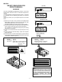
MD-R3H
SERVICE MANUAL
No. S1803MDR3H///
MD-R3H
• In the interests of user-safety the set should be restored to its
original condition and only parts identical to those specified should
be used.
• Note for users in UK
Recording and playback of any material may require consent
which SHARP is unable to give. Please refer particularly to the
provisions of Copyright Act 1956, the Dramatic and Musical
Performers Protection Act 1956, the Perfmers Protection Acts
1963 and 1972 and to any subsequent statutory enactments and
orders.
CONTENTS
Page
SAFETY PRECATION FOR SERVICE MANUAL .................................................................................................................. 2
IMPORTANT SERVICE NOTES (FOR UK ONLY) ................................................................................................................ 3
SPECIFICATIONS ................................................................................................................................................................. 3
NAMES OF PARTS ............................................................................................................................................................... 4
OPERATION MANUAL .......................................................................................................................................................... 5
DISASSEMBLY ...................................................................................................................................................................... 8
REMOVING AND REINSTALLING THE MAIN PARTS ....................................................................................................... 11
ADJUSTMENT ..................................................................................................................................................................... 14
EXPLANATION OF ERROR DISPLAY ................................................................................................................................ 29
EXPLANATION OF MECHANISM ERROR ......................................................................................................................... 30
NOTES ON SCHEMATIC DIAGRAM .................................................................................................................................. 33
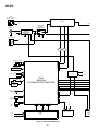
BLOCK DIAGRAM ............................................................................................................................................................... 34
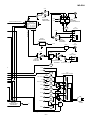
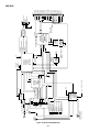
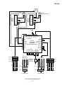
SCHEMATIC DIAGRAM/WIRING SIDE OF P.W.BOARD ................................................................................................... 40
VOLTAGE (MD MAIN PWB) ................................................................................................................................................ 58
WAVEFORMS OF CD CIRCUIT .......................................................................................................................................... 59
WAVEFORMS OF MD CIRCUIT .......................................................................................................................................... 60
TROUBLE SHOOTING ........................................................................................................................................................ 62
FUNCTION TABLE OF IC .................................................................................................................................................... 71
PARTS GUIDE/EXPLODED VIEW
PACKING METHOD (FOR UK ONLY)
SHARP CORPORATION
–1–
This document has been published to be used
for after sales service only.
The contents are subject to change without notice.
MD-R3H
SAFETY PRECATION FOR
SERVICE MANUAL
(For UK)
WARNINGS
The ael (ACCESSIBLE EMMISSION LEVEL) of the laser
power output is less than class 1 but the laser component is
capable
of emitting radiation exceeding the limit for class 1. Therefore
it is important that the following precautions are observer
during
servicing to protect your eyes against exposure to the laser
beam.
(Except for UK)
(1) When the unit case cover is removed and LOADING SW
(SW 1956) is turned on and then PLAY SW (SW 1954
mechanism PWB) is turn on in a few second.
The laser will light for several second to detect a disk.
(2) The laser power output of the pickup unit and replacement
service parts are all factory pre-set before shipment.
Do not attempt to re-adjust the laser pick-up unit during
replacement or servicing.
(3) Under no circumstances stare into the pickup lens at any
time.
(4) If laser optical unit becomes faulty, replace the complete
laser optical unit.
(5) CAUTION-USE of controls or adjustments, or pereformance
of procedures other than those specified herein may result
in hazardous radiation exposure.
LASER KLASSE 1
LUOKAN 1 LASERLAITE
KLASS 1 LASERAPPARAT
Laser Diode Properties
Material:
GaAIAs
Wavelength: 785 nm
Pulse time: Read mode: 0.8 mW Continuous
Write mode: max 10 mW 0.5 S
min cycle 1.5 S
Repetition
Laser Diode Properties
Material:
GaAIAs
Wavelength: 780 nm
Emission Duration: continuous
Laser Output: max. 0.6 mW
CAUTION - INVISIBLE LASER RADIATION WHEN OPEN AND INTERLOCKS
DEFEATED . AVOID EXPOSURE TO BEAM .
VARNING - OSYNLIG LASERSTRALNING NAR DENNA DEL AR OPPNAD OCH
SPARRAR AR URKOPPLADE . STRALEN AR FARLIG.
ADVARSEL - USYNLIG LASERSTRALING NAR DEKSEL APNES OG SIKKERHEDSLAS
BRYTES . UNNGA EKSPONERING FOR STRALEN .
VARO! AVATTAESSA JA SUOJALUKITUS OHITETTAESSA OLET ALTTIINA
NAKYMATON LASERSATEILYLLE . ALA KATSO SATEESEN .
VARNING - OSYNLIG LASERSTRALING NAR DENNA DEL AR OPPNAD OCH SPARREN
AR URKOPPLAD . BETRAKTA EJ STRALEN .
ADVARSEL - USYNLIG LASERSTRALING VED ABNING . NAR SIKKERHEDSAFBRYDERE
ER UDE AF FUNKTION . UNDGA UDSETTELSE FOR STRALING .
CAUTION - INVISIBLE LASER RADIATION WHEN OPEN AND INTERLOCKS DEFEATED
AVOID EXPOSURE TO BEAM .
VARNING - OSYNLIG LASERSTRÅLNING NÄR DENNA DEL ÄR ÖPPNAD OCH SPÄRRAR
ÄR URKOPPLADE. STRÅLEN ÄR FARLIG.
ADVARSEL - USYNLIG LASERSTRÅLING NÅR DEKSEL ÅPNES OG SIKKERHEDSLÅS
BRYTES. UNNGÅ EKSPONERING FOR STRÅLEN.
VARO! AVATTAESSA JA SUOJALUKITUS OHITETTAESSA OLET ALTTIINA
NÄKYMÄTÖN LASERSÄTEILYLLE. ÄLÄ KATSO SÄTEESEN.
VARNING - OSYNLIG LASERSTRÅLING NÄR DENNA DEL ÄR ÖPPNAD OCH SPÄRREN
ÄR URKOPPLAD. BETRAKTA EJ STRÅLEN.
ADVARSEL - USYNLIG LASERSTRÅLING VED ÅBNING NÅR SIKKERHEDSAFBRYDERE
ER UDE AF FUNKTION. UNDGÅ UDSETTELSE FOR STRÅLING.
VAROITUS! LAITTEEN KÄYTTÄMINEN MUULLA KUIN
TÄSSÄ
KÄYTTÖOHJEESSA MAINITULLA TAVALLA SAATTAA
ALTISTAA KÄYTTÄJÄN TURVALLISUUSLUOKAN 1
YLITTÄVÄLLE NÄKYMÄTTÖMÄLLE LASERSÄTEILYLLE.
VARNING - OM APPARATEN ANVÄNDS PÅ ANNAT SÄTT
ÄN I DENNA BRUKSANVISNING SPECIFICERAS. KAN
A NV ÄN DA RE N
UT S ÄT T AS
FÖR
OSY NLI G
LASERSTRÅLNING, SOM ÖVERSKRIDER GRÄNSEN FÖR
LASERKLASS 1.
–2–
MD-R3H
FOR A COMPLETE DESCRIPTION OF THE OPERATION OF THIS UNIT, PLEASE REFER
TO THE OPERATION MANUAL.
IMPORTANT SERVICE NOTES (FOR UK ONLY)
WITHSTANDING
VOLTAGE TESTER
Before returning the unit to the customer after completion of a
repair or adjustment it is necessary for the following withstand
voltage test to be applied to ensure the unit is safe for the
customer to use.
Setting of Withstanding Voltage Tester and set.
Set name
PROBE
+
AC
OUT
-
set value
SHORT-CIRCUIT
AC POWER
SUPPLY CORD
Withstanding Voltage Tester
Test voltage
4,240 VPEAK
3,000 VRMS
Set time
6 secs
Set current(Cutoff current)
4 mA
UNIT
CONNECT THE PROBE
TO GND TERMINAL
OF CHASSIS
OF
PHONO TERMINAL
SCREW
Unit
Judgment
OK: The “GOOD” lamp lights.
NG: The “NG” lamp lights and the buzzor sounds.
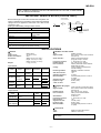
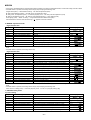
SPECIFICATIONS
General
MiniDisc recorder section
Type:
Power source:
Power consumption:
Dimensions:
Weight:
MD/CD Deck
AC 230 V, 50 Hz
20 W
Width: 430 mm (16-15/16")
Height: 118 mm (4-11/16")
Depth: 302 mm (11-15/16")
5.1 kg (11.3 lbs)
Type:
Signal readout:
Audio channels:
Frequency response:
Rotation speed:
Error correction:
Input sockets
Coding:
Socket
name
LINE IN
Socket
shape
Input
impedance
Pin socket
Reference
input level
Minimum
input level
Over
22 kohms
680 mVrms
170 mVrms
75 ohms
500 mVp-p
600 ohms
6 mVrms
Recording method:
A/D, D/A converter:
Sampling frequency:
Wow and flutter:
OPTICAL Square
IN (Optical) optical
connector
COAXIAL
(Coaxial)
Pin socket
MIC (Micro- Stereo
phone)
socket
Signal/noise ratio:
Dynamic range:
T.H.D. at 1 kHz:
Compact disc player
Type:
Signal readout:
Output sockets
Socket
name
Socket shape
Output
level
Rotation speed:
Error correction:
Load
impedance
PHONES
6.3 mm (1/4") stereo
(Headphones) socket
15 mV
32 ohms
LINE OUT
2 Vrms
50 kohms
Pin socket
MiniDisc recorder
Non-contact, 3-beem semi-conductor
laser pick-up
Stereo 2 channels/monaural
(long-play mode) 1 channel
4 - 20,000 Hz (+0/-1 dB)
400 - 900 rpm CLV, Approx.
ACIRC (Advanced Cross Interleave
Reed-Solomon code)
ATRAC (Adaptive TRansformed
Acoustic Coding)
Magnetic modulation overwrite
methood
1 bit
44.1kHz
Unmeasurable (less than ±0.001%
W. peek)
100 dB (1 kHz)
90 dB (1 kHz)
0.008%
Quantization:
Frequency response:
D/A converter:
Signal/noise ratio:
Dynamic range:
Wow and flutter:
OPTICAL
Square optical connector
OUT (Optical)
3-disc multi-play compact disc player
Non-contact, 3-beem semi-conductor
laser pick-up
200 - 500 rpm CLV, Approx.
CIRC (Cross Interleave ReedSolomon code)
16-bit linear
4 - 20,000 Hz (+0/-1 dB)
1 bit
100 dB (1 kHz)
90 dB (1 kHz)
Unmeasurable (less than ±0.001%
W. peek)
Timer/clock
Type:
Timer:
Digital clock with date function
ON/OFF, once a day
Specifications for this model are subject to change without
prior notice.
–3–
MD-R3H
NAME OF PARTS
Front panel
1
11
2
3
4
5
12
TOC DISC TRACK DATE
12
13
MONO LP PRGM
TOTAL
REMAIN
RANDOM
TIMER REC
14 1516 17 18
21
22
6
19
7
4
0dB
8
OVER
9
10
AM 1 2 3 4 5 6 7
PM 8 9 10 11 12 13 14
CLOCK 15 16 17 18 19 20
20
23 24 25
26 27
28
29
30
31
32
33
34 35
36 37
38 39 40 41 42 43 44 45
46
24. CD Track Select Button
25. Cue/Review Button:
26. Display/Character Button
27. Remote Sensor
28. MD Loading Slot
29. Record Level Control
30. Microphone Socket
31. On/Stand-by Button
32. CD Stop Button:
33. CD Play/Pause Button:
34. Headphone Socket
35. Headphone Level Control
36. CD Edit Button
37. Program Button
38. Jog Dial (Next/Previous)
39. Enter Button
40. Delete/Clear/Timer Button
41. Name/TOC Edit Button
42. Input Select Button
43. Record Button:
44. MD Stop Button:
45. MD Play/Pause Button:
46. MD Eject Button:
1. MD TOC Indicator: TOC
2. Total Time Indicator
3. Disc Name Indicator
4. Track Name Indicator
5. Data Indicator
6. Level Meter/Character Information Display
7. Recording Level indicator
8. Recording Level Too High Indicator
9. Music Calender
10. More Tracks Indcator
11. Pause Indicator:
12. Record Indicator:
13. Play Indicator:
14. Monaural Long-Play Mode Indicator
15. Programme Indicator
16. Repeat Indicator:
17. Remaining Time Indicator
18. Random Play Indicator
19. Timer Playback/Timer Recording Indicator
20. Clock Indicator
21. CD Trays
22. CD Direct Play Buttons and Indicators
23. CD Open/Close Buttons:
Rear panel
1. AC Power Lead
2. Coaxial Input Socket (Digiral)
3. Optical Input/Output Sockets
(Digital)
4. Line Input/Output Sockets
(Analogue)
5. Reset Button
1
2
–4–
3
4
5
CLOCK
–5–
CLOCK
The unit will enter the time setting mode.
Set the “day” repeating steps 4 and 5.
Set the “month” repeating steps 4 and 5.
Press the ENTER button to set the “year”.
When you turn the jog dial and let go, the year will change
up or down by one.
The year 2000 or later is set as follows:
[00] indicates the year 2000.
[01] indicates the year 2001.
The range of dates that can be entered is from January 1,
1997 to December 31, 2099.
Set the “year” using the jog dial.
The unit will enter the date setting mode.
Within 10 seconds, press the ENTER button.
Within 10 seconds, turn the jog dial until “TIME ADJUST”
appears.
Press the ON/STAND-BY button to turn the power on and
press the TIMER button.
2
3
4
5
6
7
8
9
10
11
Time setting mode
DATE
Each time the button is pressed,
the display will change.
5
6
7
4
3
2
1
Setting the date
23
7
TIMER
DELETE/CLEAR
CLOCK
Date setting mode
DATE
ENTER
When recording, the date and time are recorded on the Minidisc.
1. Direct Key Buttons
2. Play Mode Button
3. Music Scan Button
4. Input Select Button
5. Display Button
6. Auto Mark Button
7. Time Button
8. MD Track Up/Cue Button:
9. MD Track Down/Review Button:
10. CD Track Down/Review Button:
11. CD Track Up/Cue Button:
12. Program Button
13. Clear Button
14. Synchro Record Button:
15. Record Cancel Button
16. Record Button:
17. Record Mode Button
18. MD Stop Button:
19. MD Play/Pause Button:
20. CD Play/Pause Button:
21. CD Stop Button:
22. CD Play buttons:
1-3
23. On/Stand-by Button
6
54
3
2
1
ON/
STAND-BY
SETTING THE CLOCK
MD-R3H
Names of controls
1
12
13
14
15
16
17
18
19
20
21
22
OPERATION MANUAL
–6–
DATE
DATE
DATE
DATE
0.2 - 6 m (8" - 20')
REMOTE CONTROL
11
10
9
8
(Continued)
15
ENTER
15
CLOCK
CLOCK
CLOCK
CLOCK
TIMER
DELETE/CLEAR
When you turn the jog dial and let go, the hour will change
up or down by one. When you turn and hold it, the hour will
change continuously.
The clock uses the 24-hour system.
Set the “hour” using the jog dial.
Replace the batteries if the control distance decreases or
operation becomes erratic.
Periodically clean the transmitter window on the remote
control and the sensor on the main unit with a soft cloth.
Exposing the sensor on the main unit to strong light can
interfere with operation. Change the lighting or the direction
of the unit.
Keep the remote control away from moisture, excessive heat,
shock, and vibrations.
The remote control's usable range is between 0.2 m (8") and
6 m (20') away from the sensor.
Notes concerning use:
Aim the remote control at the remote control sensor within 30o
with no obstacles, and operate as shown.
Proper use of the remote control
Once you have set the date and time, “TIME ADJUST” will
not be displayed in step 2. Turn the jog dial to make the date
and time appear.
If you don't need to change the settings, just press the ENTER
button without turning the jog dial again.
See “Setting the clock”.
Resetting the date and time
After pressing the TIMER button, turn the jog dial until the date
and time are displayed.
Checking the date and time
When the ENTER button is pressed, the clock will show the
correct time.
9 Press the ENTER button to set the “hour”.
10 Adjust the “minute” using the jog dial.
11 Press the ENTER button to set the “minute”.
8
After step 7, described in the “Setting the date” section
Setting the time
SYMPTOM
POSSIBLE CAUSE
REMEDY
POSSIBLE CAUSE
REMEDY
Clean the disc.
Load the disc with the correct side up.
SYMPTOM
The power cannot be turned on from the
remote control.
The remote control does not function or
does not operate properly.
Load a disc.
No disc has been loaded.
Connect the AC power lead.
Operate it within a range of 0.2 m (8") to
6 m (20') and within an angle of 15 o to
either side of centre.
The remote control is operated from an
incorrect distance or angle.
Is the AC power lead plugged in?
Replace the batteries.
The batteries inside the remote control
are dead.
REMEDY
Insert properly.
The batteries (polarity) are not inserted
properly.
POSSIBLE CAUSE
Remove the disc and leave the power
turned on. The unit should function properly in about 1 hour.
Has condensation formed inside the unit?
Playback sounds are skipped.
Remote control
Place the unit on a firm, level surface free
from vibration.
Is the unit located near excessive vibrations?
Is the unit located near excessive vibration?
Replace the disc.
Place the unit on a firm, level surface
free from vibration.
Put in another recordable disc with recording space on it.
Can you see the “TOC FULL” message
in the display?
Is the disc scratched?
Replace it with a recordable disc.
Did you try to make recording on a playback-only MiniDisc?
REMEDY
Slide the accidental erase prevention tab
back to its original position.
POSSIBLE CAUSE
Is the MiniDisc protected against accidental erasure?
Playback stops in the middle of a track,
or playback is not performed properly.
Even though a disc has been loaded,
“NO DISC” or “ERROR” is displayed.
A recording cannot be made.
SYMPTOM
MD recording and playback
Load the correct disc.
Playback stops in the middle of a track, The disc does not satisfy the standards.
Is the unit located near excessive vibra- Place the unit on a firm, level surface free
or playback is not performed properly.
tions?
from vibration.
Playback sounds are skipped.
Has condensation formed inside the unit? Remove the disc and leave the power
turned on. The unit should function properly
in about 1 hour.
Even though a disc has been loaded, "NO The disc is loaded up-side down.
DISC" or "ERROR" is displayed.
The disc is very dirty.
SYMPTOM
CD playback
It is recommended that you use an outdoor aerial.
Radios make unusual noise or the picture
on the TV screen is distorted.
Try setting it again.
Turn the power off and on again, and
then retry the operation.
When a radio or TV which uses an indoor aerial is placed near the unit, the
picture on the TV screen may be distorted or the radio may not function properly.
Did a power failure occur?
When a button is pressed, the unit does
not respond.
The clock is wrong.
General
If this unit functions abnormally during operation, first check the following items. If the unit continues to function abnormally,
or if an abnormality appears other than listed below, turn off the player's power and disconnect the AC power plug, then
consult your SHARP dealer or service personnel.
If a problem occurs
TROUBLESHOOTING
MD-R3H
–7–
A track cannot be edited.
Recording cannot be performed correctly due to
vibration.
Since this disc has scratches on it, the
recording operation was skipped.
The CD changer is not working properly.
Incorrect digital signals are input.
The disc is damaged or there is no TOC on the
disc.
The disc is out of recording space.
There is no space left to record the remainder
of the CD.
The proper focus cannot be obtained.
The unit has determined that it is out of order
by performing a self-diagnosis.
There is a mechanical problem and the disc is
not working properly.
The number of characters for the disc name or
track name exceeds 100.
A disc has not been loaded.
The disc data cannot be read.
The data recorded on this disc is not audio data.
You tried to record on a playback-only disc.
The data of disc names and track names are
not able to move from playback-only discs.
The MiniDisc is write protected.
The temperature is too high.
The disc has a large amount of damage.
TOC information cannot be read.
The MD does not meet the specifications for
MDs.
There is no space left for recording character
information (track names, disc names, etc.)
The unit has determined that it is abnormal by
performing a self-diagnosis.
The TOC information on this disc does not
meet the MD specifications or it cannot be read.
The TOC information could not be created
properly due to a mechanical shock or to
scratches on the disc.
The data contains an error.
Music is not being recorded.
Can't EDIT
Can't REC
DEFECT
CH ERROR
Din UNLOCK
DISC ERR
DISC FULL
EDIT OVER
FOCUS ERROR
MD ERROR
MECHA ERR*
NAME FULL
*NO DISC*
NOT AUDIO
PLAYBACK MD
PROTECTED
TEMP OVER
TOC ERR*
TOC FULL*
TOC W ERROR
U TOC ERR*
U TOC W ERR
? DISC
0 0:00
*: Number or symbol
You tried to record from a disc which you are
not allowed to copy.
Can't COPY
Meaning
Nothing is recorded.
(Neither music nor a disc name have been
recorded on this MD.)
BLANK MD
Error messages
When an error message is displayed, proceed as follows:
(Continued)
Remedy
Replace the disc with a recorded disc.
Replace the disc with another disc.
Press the ON/STAND-BY button to enter the
stand-by mode, and try to write the TOC again.
(Remove any source of shock or vibration whilst
writing.)
Replace it with another disc.
Erase all the data, and try recording.
Ask the store where you purchased this unit,
about repairs.
Replace it with another recordable disc.
Replace the disc with another disc.
Press the ON/STAND-BY button to enter the
stand-by mode, and wait for a while.
Move the write protection tab back to its original
position.
Replace it with a recordable MiniDisc.
Edit only the sound.
Select another track.
Replace the disc.
Load a disc.
Reload the disc.
Shorten the disc or track name.
Press the ON/STAND-BY button to enter the
stand-by mode, and press the
button.
Ask the store where you purchased this unit,
about repairs.
Reload the MiniDisc.
Replace the MD with another recordable disc.
Replace the disc with another recordable disc.
Reload the disc or replace it.
Connect correct digital signals.
Use the analogue input socket.
Press the ON/STAND-BY button to enter the
stand-by mode, and disconnect the AC power
lead from the AC socket. Then connect the AC
power lead, and turn on the power again.
Replace the disc with another recordable disc.
Move the unit away from the source of vibration.
Change the stop position of the track and then
try editing it.
Replace it with another disc which you can
copy from (regular CD).
Replace the disc with a recorded disc.
1,4,5
2
TRANSPORTING THE UNIT
2
1
2
3
When the RESET button is pressed, all of the settings
in memory will be erased.
If strange sounds, smells or smoke come out of the unit
or if a foreign object falls into the unit, turn off the power,
unplug the AC power lead from the AC socket, immediately. Contact the shop where you purchased the
unit.
Pen, pencil, etc.
RESET
Unplug the AC power lead from the AC socket.
Wait about 20 - 30 seconds and then plug the AC power
lead back into the AC socket.
Press the RESET button on the back of the unit.
If this product is subjected to strong external interference (mechanical shock, excessive static electricity, abnormal supply voltage due to lightning, etc.) or if it is
operated incorrectly, it may malfunction or the display
may not function correctly. If such a problem occurs,
do the following:
If a problem occurs
5
6
4
1
2
3
Make sure the message on the display has changed from
"GOOD BYE!" to "TIME ADJUST", and then unplug the AC
power lead from the AC socket.
Press the ON/STAND-BY button to enter the stand-by mode.
Make sure "TIME ADJUST" appears in the display, then press
the ON/STAND-BY button to turn the power on again.
When the RESET button is pressed, all of the settings in memory will be erased.
Press the RESET button on the rear of the unit.
Remove all discs CDs/MD from the unit.
Press the ON/STAND-BY button to turn the power on.
When transporting the unit, proceed as follows:
If a power failure occurs or the AC power lead is disconnected for about 10 minutes, when power is restored,
the TOC will be written on the disc.
If the AC power plug is disconnected from the AC socket
or a power failure occurs during recording (before the
TOC information has been recorded on the disc), the
audio portion being recorded at that time will be erased.
When a recording is being added to a MiniDisc which
already has a recording on it, if the TOC is not updated
before the power failure, the added recording will be
erased.
If a power failure occurs during recording
● If this happens, remove the disc, and open the disc tray.
The condensation should evaporate in approximately 1
hour. The unit will then function properly.
When the unit has condensation inside, the disc signals
cannot be read, and the product may not function properly.
Shortly after turning on a heater.
When the unit is placed in a room where there is excessive steam or moisture.
When the unit is moved from a cool place to a warm
place.
In the following cases, condensation may form inside
the unit.
Moisture condensation
(Continued)
MD-R3H
MD-R3H
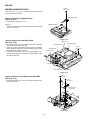
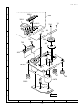
DISASSEMBLY
STEP
REMOVAL
PROCEDURE
FIGURE
8-1
1
Top Cabinet
1. Screw ..................... (A1) x5
2
Rear Panel
1. Screw ..................... (B1) x5
8-2
3
MD Unit
1. Screw .................... (C1) x4
2. Flat Cable ............... (C2) x1
3. Socket .................. (C3) x1
8-2
4
Front Panel
1. Screw .................... (D1) x6
2. Flat Cable ............... (D2) x1
3. Socket ................... (D3) x4
8-3
5
CD Changer Block 1. Screw ...................... (E1) x4
(with CD Servo/
2. Socket ..................... (E2) x4
CD Changer PWB)
8-3
6
Main PWB
1. Screw ..................... (F1) x6
(with Transformer)
8-3
7
Mic PWB
1. Screw ................... (G1) x2
8-4
8
Headphones PWB 1. Screw ....................... (H1) x2
8-4
9
Jog Dial
1. Knob ....................... (J1) x1
2. Nut .......................... (J2) x1
8-4
10
Display PWB/
Switch PWB
1. Knob ....................... (K1) x2
2. Screw ................... (K2) x13
8-4
11
Switch PWB
1. Screw ..................... (L1) x4
8-4
12
CD Servo PWB
(Note1)
1. Screw ................... (M1) x3
2. Socket ................... (M2) x3
9-1
13
CD Changer PWB 1. Screw ....................... (N1) x2
9-1
14
Tray Switch PWB 1. Screw ..................... (P1) x1
9-1
15
CD Mechanism
1.Screw ..................... (Q1) x2
2. Top Board ............. (Q2) x1
3. Disc Holder ............ (Q3) x3
4. Disc Tray ............... (Q4) x3
5. Screw .................... (Q5) x1
6. Mechanism Holder
Guide ..................... (Q6) x1
7. Mechanism Holder . (Q7) x1
8. Screw .................... (Q8) x4
9-2
Top Cabinet
(A1)x1
ø3x10mm
Caution on Disassembly
Follow the below-mentioned notes when disassembling
the unit and reassembling it, to keep it safe and ensure
excellent performance:
1. Take the minidisc out of the unit.
2. When disassembling the machine, be sure to withdraw
the power plug from the socket in advance.
3. When disassemble the parts, remove the nylon band or
wire holder as necessary.
To assemble after repair, be sure to arrange the wires as
they were.
If a screw of different length is fitted to the MD mechanism (the screw of the part to be fitted to the MD
mechanism chassis), it may contact the optical pickup,
resulting in malfunction.
4. When repairing, pay due attention to electrostatic charges
of IC.
(A1)x1
ø3x10mm
(A1)x3
ø3x10mm
Figure 8-1
MD Unit
(C1)x4
ø3x6mm
Front Panel
(C3)x1
(C2)x1
(B1)x5
ø3x10mm
Rear Panel
Figure 8-2
(D1)x1
ø3x8mm
(F1)x2
ø3x10mm
(E2)x1
(F1)x2
ø4x8mm
Washer
Front Panel
(D3)x1
(D2)x1
(F1)x2
ø3x10mm
(E2)x1
Main PWB
(E2)x2
(E1)x1
(D3)x3
ø3x10mm
(E1)x1
ø3x10mm
16
MD Mechanism
Unit
1. Screw .................... (R1) x4
9-3
17
MD Main PWB
1. Screw ..................... (S1) x4
2. Socket .................... (S2) x6
9-4
18
MD Mechanism
1. Screw ..................... (T1) x4
9-5
CD Changer
Block
Mic PWB
(D1)x1
ø3x8mm
(E1)x2
ø3x10mm
Figure 8-3
(K1)x1
Display PWB
(J2)x1
(J1)x1
Washer
(G1)x2
ø2.6x10mm
(K2)x2
ø2.6x10mm
Note 1. After removing the connector for the optical pickup
from the connector wrap the conducitive aluminum
foil around the front end of connector so as to protect
the optical pickup from electrostatic damage.
(D1)x4
ø3x8mm
(K1)x1
Headphones
PWB
Switch PWB
Front Panel
(K2)x11
Switch PWB
ø2.6x10mm
(L1)x4
(H1)x2
ø2.6x10mm ø2.6x10mm
Figure 8-4
–8–
MD-R3H
Shield Case
CD
Servo PWB
CD Changer
Block
(R1) x 2
ø3 x 6mm
Tray
Switch
PWB
(M2)x3
(M1)x3
ø3x10mm
(N2)x2
(P1)x1
ø2x7mm
(R1) x 2
ø3 x 6mm
MD Mechanism
Unit
CD Changer PWB
(N1)x2
ø2.6x10mm
(Remove 4 soldering joints).
Figure 9-1
Figure 9-3
(Q3) x1
(S2) x 1
Push.
(Q1) x2
ø2 x7mm
(Q5) x1
ø2.6 x12mm
Pickup Flexible
PWB (*1)
Pawl
MD Main PWB
(S1) x 4
ø1.7 x 3mm
(Q6) x1
Pull
(Q7) x1
(S2)x1
Spring
CD
Mechanism
(Q2) x1
(Q8) x4
ø2.6 x10mm
Normal state
(*1) After disconnecting the optical
pickup flex PWB from the
connector wrap the front end of
flex PWB in conductive aluminium
foil so as to prevent electrostatic
damage of optical pickup.
(S2) x 1
(S2) x 3
Turn clockwise the
main cam to raise the
CD mechanism up to
the uppermost position.
Disc Tray 1
Frame
Disc Tray 2
Disc Tray 3
(Q4) x3
1
2
3
Figure 9-4
Press in turns the arrow
parts, starting with the
uppermost one, to
withdraw the disc trays
MD Mechanism
Push the pawl of disc tray
with a proper screwdriver.
Back surface
Pawl
Pawl
Disc Tray 1
Disc Tray 2
Disc Tray 3
(After drawing out the disc trays 1, 2, and 3, turn
over the mechanism unit, push two pawls, and
remove successively the three disc trays from the
mechanism unit, starting with the disc tray 3.
Thereby the CD mechanism shown in the right
figure can be removed.)
(T1)x4
ø1.7x8.9mm
Figure 9-2
Figure 9-5
–9–
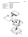
MD-R3H
• Jog knob replacement procedure
NUT
Jog Knob
Jog Decoration
FL Window
Jog Decoration
Front Panel
VOLUME
Display PWB
Jog Knob
Push directly the jog knob with pliers etc.
Figure 10-1
Display PWB
Remove the pawl of jog decoration with fine piece
such as tweezers, press, and remove the jog knob.
Only push out on the jog knob itself.
Figure 10-2
– 10 –
MD-R3H
REMOVING AND REINSTALLING THE MAIN PARTS
(A1) x2
ø2.6 x5mm
CD MECHANISM SECTION
For the procedure to remove the CD mechanism from the
main unit, refer to Disassembling Procedure, Steps 1, 5, 11,
and 14.
How to Remove the optical pickup
(See Fig. 11-1.)
Stop Washer
(A3) x1
Pickup
CD
Mechanism
1. Remove the screws (A1)x 2 pcs., to remove shaft (A2)x 1
pc.
2. Remove stop washer (A3)x 1 pc., to remove gear (A4)x 1 pc.
3. Remove the optical pickup.
Note:
After disconnecting the optical pickup connector wrap the
front end of connector in conductive aluminum foil so as to
prevent damage to the optical pickup by static electricity.
Shaft
Gear (A2) x1
(A4) x1
Figure 11-1
(B2) x2
ø2.6 x4mm
(B2) x2
ø2.6 x4mm
How to Remove the tray motor/main cam motor
(with CD changer PWB)
(See Fig. 11-2.)
Belt
(B1) x1
1. Remove the front cabinet, and remove the CD changer from
the rear cabinet. After that, disassemble as shown in the
figure.
2. Remove the belts (B1)x 2 pcs., from the motor side.
3. Remove the screws (B2)x 4 pc.
4. Remove the tray motor and main cam motor.
Belt
(B1) x1
Main Cam
Motor
Tray Motor
CD Changer PWB
Figure 11-2
Turn the main cam clockwise,
and raise the CD mechanism
and disc holder up to
uppermost position.
How to remove the CD disc
(When CD is in playback state)
(See Fig. 11-3.)
Disc Holder
CD Disc
1. Remove the front cabinet.
2. Remove the CD changer from the rear cabinet.
3. Remove the CD disc as shown in the figure.
CD CHanger
Block
(When CD is in playback state.)
Figure 11-3
Turn the main cam clockwise,
and raise the CD mechanism
and disc holder up to
uppermost position.
How to remove the CD disc
(When CD exists in the tray)
(See Fig. 11-4.)
Disc Holder
CD Mechanism
1. Remove the front cabinet.
2. Remove the CD changer from the rear cabinet.
3. Remove the CD disc from the tray as shown in the figure.
CD Changer
Block
CD Disc
1
2
3
Press in turns the arrow
parts, starting with the
uppermost one, to
Disc Tray 1
withdraw the disc trays
Disc Tray 2
Disc Tray 3
(When CD exists in the tray.)
Figure 11-4
– 11 –
MD-R3H
(A1)x1
ø1.7x5mm
MD MECHANISM SECTION
Perform steps 1, 3, 15 to 17 of the disassembly method to
remove the MD mechanism.
Magnetic Head
How to remove the magnetic head
(See Fig. 12-1)
1. Remove the screws (A1) x 1 pc.
Caution:
Take utmost care so that the magnetic head is not damaged
when it is mounted.
MD Mechanism
Figure 12-1
How to remove the cartridge holder
(See Fig. 12-2)
Slider Lever
1. Open the rpller arm lever in the arrow direction, and lower
the clamper lever to the rear side.
2. Apply +5V to the red line side of blue connector of loading
motor, push the rack gear in the arrow direction to move the
cam plate lever until tick is heard.
3. Remove the screw (B1) x1 pc., and the spring (B2) x1 pc.,
fitted to the holder arm, and shift the cartridge holder to the
left side to remove it.
Roller Arm Lever
Cartridge Holder
(B1) x1
Ø1.7x5mm
Loading Motor
Clampa Lever
Lack Gear
Cam Plate Lever
(B2) x1
Figure 12-2
(C1)x1
Ø1.7x3mm
How to remove the mechanism switch PWB
(See Fig. 12-3)
1. Remove the screws (C1) x 2 pcs., and remove the mechanism switch PWB.
(C1)x1
Ø1.7x9.5mm
MD Mechanism
Switch PWB
Figure 12-3
– 12 –
MD-R3H
How to remove the sled motor/loading motor
(See Fig. 13-1)
1. Remove the screws (D1) x 1 pcs., and remove the sled
motor/loading motor.
(D1)x2
Ø1.7x2mm
(D1)x2
Ø1.7x2mm
Caution:
Be careful so that the gear is not damaged.
(The damaged gear emits noise during searching.)
Loading
Motor
Sled Motor
Figure 13-1
How to remove the spindle motor
(See Fig. 13-2)
1. Remove the screws (E1) x 3 pcs., and remove the spidle
motor.
Caution:
Be careful so that the turntable is not damaged.
Turntable
(E1)x3
Ø1.7x2.5mm
Spindle Motor
Figure 13-2
How to remove the optical pickup
(See Fig. 13-3)
(F1)x3
Ø1.7x9.5mm
1. Remove the screws (F1) x 3 pcs.
Optical Pickup
Caution:
Be careful so that the gear is not damaged.
(The damaged gear emits noise during searching.)
Figure 13-3
– 13 –
MD-R3H
ADJUSTMENT
CD SECTION
Extension cable
When making adjustment or checking operation, use the following extension cable as necessary.
Type
A
Extension cable
Parts No.
For CD PWB (TP751, 6-pin)
QCNWK0043AFZZ
CD SERVO PWB
A
1
TP751
1
6
6
Extension cable for
CD Servo PWB
QCNWK0043AFZZ
CNP700A
BI851/CNS552
CNP751
CNS903
1
10
CNP752
Figure 14
CD circuit adjustment
1. Preparation for adjustment
Setting the CD TEST mode
Test mode
Setting procedure
Remarks
CD test mode 0
Holding down the CD direct play 1
button and the ENTER butto plug in
AC code (or press the RESET
switch).
Without IL
CD test mode 1
IPress the [CD-PLAY] button.
Laser ON
CD test mode 2
Press the [CD-PLAY] button.
(2nd time)
Focus servo ON
Indication
CD test mode 1
CD test mode 2
CD test mode 3
Press the [CD-PLAY] button.
(3rd time)
When the spin servo is on, the disc
motor rotates.
CD test mode 3
CD test mode 4
Press the [CD-PLAY] button.
(4th time)
Tracking servo ON
CD test mode 5
Press the [CD-PLAY] button.
(5th time)
Track No. and time are indicated.
CD test mode 4
CD test mode 5
– 14 –
MD-R3H
Button operation in CD test mode
1. [STOP]
2. [
3. [
]
]
4. [DISP]
6.Hold down [CD-PLAY] for 500 msec
: Specific operation is stopped, resulting in TEST mode waiting state. The pickup slide
is kept in stop state.
: The pickup slides toward the external periphery.
: The pickup slides toward the internal periphery.
When the switch (Pu_IN) is on, the slide is stopped.
: When this switch is pressed in TEST 4 or later, it is accepted, and the mode is changed
directly to TEST 3.
(Tracking servo OFF)
: This button is accepted in the TEST waiting state, and mode is changed directly to
TEST 5.
Caution
1.Even when the sub-code cannot be read during playing, the [STOP] button must be accepted to perform the STOP operation.
2.When the [CD-EJECT] button is pressed, the tray must be opened after normal STOP operation.
2. Adjusting the servo unit
Set all the half-fixed resistors in the mechanical center position.
Adjustment classification
Adjusting object Setting/adjusting procedure
Connection of measuring instrument
Set the CD test mode 0, and shift the pickup to the center.
Set the CD test mode 1. (Make sure that laser lights.)
After loading the disc set the test mode 2.
(Make sure that the focus servo is on. The disc does not rotate but mechanical tone is heard.)
Set the CD test mode 3. (The spin servo is turned on, and the disc turns.)
Tracking error balance adjustment
VR751
*1 (Figure 16-1)
Pin 6 (1/2Vcc) and pin 4 (TG1) of TP751
Get the same waveform on
CH1 and CH2. *2
Pin 4 (TG1), pin 2 (TG2) and pin 6 (1/2Vcc)
of TP751 (Relay circuit is used)
Set the CD test mode 4. (Tracking servo ON)
Tracking gain adjustment
VR752
Set the test mode 5, and make sure that track No. and time are indicated.
Apply a black tape to the disc, and play back this part. (Figure 16-2). (It is allowed to apply any mode in addition to test mode.)
Focus offset adjustment
VR753
*3
Pin 6 (1/2Vcc) and pin 1 (FG1) of TP751 *4
Tracking offset adjustment
VR754
*5
Pin 6 (1/2Vcc) and pin 4 (TG1) of TP751 *6
*1: Taking 1/2Vcc as a reference DC level, make an adjustment to get vertical symmetry of waveform (Figure 16-1) with respect
to the reference DC level.
(Amplitude 0.5 to 1.5 Vp-p) (As the optical pickup has been adjusted before shipping, adjustment is required only when
adjustment disturbance is found.)
*2: Input oscillation frequency 1.5 kHz, 300 mVrms
*3: Make an adjustment so that the error waveform is minimized (Figure 16-3), noise (track jump sound) ceases during audio output
monitoring and clear playback is ensured.
*4: The proper measurement range of oscilloscope is 50 mV, 0.5 ms.
Connect the trigger to the pin 39 (HFD) of IC750, apply coupling on DC (-) slope, and observe waveform in the normal trigger
mode.
*5: Make an adjustment so that the error waveform becomes uniform and is minimized (Figure 16-3), noise (track jump sound)
ceases during audio output monitoring, clear playback is ensured and sound skip and pause state do not occur.
*6: The proper measurement range of oscilloscope is 0.1V, 0.5 ms. The trigger is the same as stated in the note*4 above.
Reference: If the error waveform contains significant noise and is not clear, observe the waveform, using the low-pass filter (Figure
16-4).
– 15 –
MD-R3H
Vertically
symmetrical
waveform
0.5~1.5Vp - p
Reference
CD level
1/2 VCC
Adjust to get uniform and minimized
error waveform.
Figure 16-1 TRACKING ERROR BALANCE
Apply a black tape
(1.2 to 1.5 wide).
Figure 16-3 FOCUS OFFSET/TRACKING OFFSET
FG1
TP751, pin 1
TG1
TP751, pin 4
27kΩ
Waveform
observation
point
820P
1/2 VCC
Figure 16-4 LOW-PASS FILTER
2.2K
TP751,
pin 4
(TG1)
It is allowed use any disc in addition
to test disc.
Do not apply the black tape to the
initialization part (TOC).
0.0082
100K
TP751,
pin 6
(1/2Vcc)
820P
CH - 1
VV
Signal
transmitter
100K
820P
100K
TP751,
pin 2
(TG2)
Figure 16-2 FOCUS OFFSET/TRACKING OFFSET
100K
VV
CH - 2
0.0082
2.2K
Figure 16-5 TRACKING GAIN RELAY CIRCUIT
Do not plug in or unplug the optical pickup
connection cable while power is on.
Otherwise damage may occur.
For your safety do not attempt to adjust
the half-fixed resistor for laser power
adjustment.
1
2
3
4
5
6
CD SERVO PWB
CNP700A
TP751
FG1
FG2
HF
TG1
FG2
1/2Vcc
CNS903
1
6
TP751
VR754
VR753
VR751
VR752
OPTICAL PICKUP PWB
TRACKING
OFFSET
FOCUS
OFFSET
Figure 16-6 ADJUSTMENT POINTS
– 16 –
TRACKING
GAIN
TRACKING
ERROR BALANCE
MD-R3H
TEST MODE
1) Mode there are 5 kinds TEST MODE as below.
MODE
PUSH KEY
A) MD TEST MODE
ENTER
PLAY
B) AUDIO TEST MODE
CUE
REVIEW
C) KEY TEST MODE
CUE
ENTER
D) RECORDING TEST MODE
ENTER
REC
E) MD TEST2 MODE (DATA MONITOR MODE)
ENTER
STOP
2) How to start and quit TEST MODE.
AC Supply On or push RESET KEY after push two keys.
In all TEST MODE. Power Off (POWER KEY) is quit TEST MODE.
3) TEST MODE description.
A) MD TEST MODE (ENTER+PLAY)
Disp. Will be "AUT YOBI". In this mode push PLAY KEY in mean product alignment's auto adjust mode.
(Disp. Will be "AUTO AJST". In this mode push PLAY KEY in mean auto adjust mode by disc condition.
Then push PLAY KEY again. It start play and display will be "a__C__". The 4 digits after "a" are address.
After "C" are error rate.)
PUSH KEY NAME
ACTION
ENTER
Servo adjust mode or menu from adjust mode.
TIMER
REC. and P.B. mode or to menu from REC.mode.
NAME
Other menu select.
REC
Reverse menu select.
PLAY
Selected menu execution.
STOP
Execute stop.
CUE
Slide motor (PIC) move to out-side.
REVIEW
Slide motor (PIC) move to in-side.
JOG. UP *1
Manual alignment +1, loading motor on (OUT).
JOG. DOWN *1
Manual alignment -1, loading motor on (IN).
POWER
Test mode quit and power off.
EJECT
Disc eject.
*1. Jog. Up/Jog. Down key effect for loading motor control when display panel "tsm____e__". (Push STOP KEY some times
to disp. "tsm____e__".)
NOTE. MD test are necessary mode only for MD Unit.
B) Audio test mode (CUE+REVIEW)
This mode is key examination mode for a set with in MD-unit.
Automatically set recording mode.
Digital opt. Digital coax and analog are effective.
Test mode start is REC KEY push after disc toc. Read.
REC KEY push
1) Record form analog function by 3 sec time.
2) Record form digital opt. Function by 3 sec time.
3) Record from digital coax. Function by 3 sec time.
4) Record stop.
Note. 1) If digital function is din unclock. Skip to follwing next function.
2) Digital synchronize level is -50 dB.
Analog synchronize level is -47 dB.
C) Key test mode (CUE+ENTER)
This mode is key examination mode for a set with out MD-unit.
This mode indicate destination as below dot display.
– 17 –
MD-R3H
KEY TEST
KEY NAME
KEY NAME
ILLUMINATE
SEGMENT
ILLUMINATE
SEGMENT
TIMER
10 ROW DOT
INPUT SELECT
DISPLAY
11 ROW DOT
EJECT
TOC
7 ROW DOT
REVIEW
ALL
PLAY
4 ROW DOT
CUE
PM
STOP
5 ROW DOT
ENTER
8 ROW DOT
REC
6 ROW DOT
JOG. UP
17 (M.C.)
NAME
9 ROW DOT
JOG. DOWN
18 (M.C.)
TIME
AM
PROGRAM
PRGM
D) Recording test mode (ENTER+REC)
This mode is auto recording repeat mode.
After disc full. Erase all and rec start again.
MD SECTION
1. Preparation for adjustment
Test disc
Type
1
2
3
Test disc
Part No.
High reflection disc TGYS1 (SONY)
RRCDT0101AFZZ
Low reflection disc Recording minidisc
UDSKM0001AFZZ
Head Adjusting transparent RRCDT0103AFZZ
Extension Cable (See Fig. 28-4)
Type
1
2
3
4
3
Part No.
Extension PWB for servicing
Extension Connector (2 Pin)
Extension Connector (6 Pin)
Extension Cable (5 Pin)
Extension Cable (28 Pin)
RUNTK0457AFZZ
QCNWK0059AFZZ
QCNWK0107AFZZ
QCNWK0109AFZZ
QCNWK0108AFZZ
2. Test mode
Test mode setting method
1. Holding down the ENTER button and MD
(PLAY/PAUSE) button, press the RESET button.
(State A is changed to state B .)
2. Insert the playback disc 1 (high reflection disc) or recording disc 2 (low reflection disc). (State C is set.)
Thus, the test mode state is set.
A tsm
TEST
e
: TEST MODE
STOP state
represents version of MD microcomputer.
(When the MD (STOP) button is ressed in the C state, the indication A
is restored. To restore C again, press the ENTER button.)
B EJECT
TEST
C AUT YOBI
TEST
Entering the specific mode
Whenever the CD
(PLAY/PAUSE) button is pressed, the mode is changed.
AUTO pre-adjustment
AUTO adjustment
RESULT SUB
EEPROM setting
MANUAL adjustment
RESULT
MANUAL pre-adjustment
• Canceling the test mode
• When the RESET button is pressed, the test mode is canceled, and the POWER OFF state is set.
• If you press the POWER button, the test mode will be can celled after writing into EEPROM and the mode without auto adjustment
will be actirated.
– 18 –
MD-R3H
• Test Mode
1. AUTO pre-adjustment mode
• Automatic pre-adjustment is performed. (After adjustment the grating adjustment mode is set.)
• The adjustment value is output with the aid of system controller interface.
2. AUTO adjustment mode
• Automatic adjustment is performed.
• The adjustment value is output with the aid of system controller interface.
• Continuous playback is performed. (Error rate indication, jump test)
3. RESULT sub-mode
• The measurement value, set value and calculated value are indicated.
• The set value is changed manually (in servo OFF state).
4. RESULT mode (final adjustment)
• The set value (after calculation) is indicated.
• The set value is changed manually (in servo OFF state).
5. MANUAL pre-adjustment mode
• RF side manual adjustment is performed.
• Focus and tracking signal ATT manual adjustment is performed.
• Focus and tracking signal offset setting is performed.
6. MANUAL adjustment mode
• Focus and tracking signal ATT manual adjustment is performed.
7. EEPROM setting mode
• Various coefficients of digital servo are changed manually.
• Each servo is set to ON individually.
• Temperature detection terminal voltage is measured, and the reference value is determined.
8. TEST-PLAY mode
• Continuous playback from the specified address is performed.
• C1 error rate measurement, ADIP error rate measurement.
9. TEST-REC mode
• Continuous recording from the specified address is performed.
• Change of record laser output (servo gain is also changed according to laser output)
10. INNER mode
• The position where the INNER switch is turned on is measured.
11. EJECT mode
• TEMP setting (of EEPROM setting)
• CONTROL setting (of EEPROM setting)
• Setting of laser power (record/playback power)
1. AUTO pre-adjustment mode (Low reflection disc only)
Step No.
Step 1
•
Setting Method
Remarks
Testmode STOP state
Display
[tsm
AUTO pre-adjustment menu
]
A U T O
]
Step 2
Press once the ENTER button.
Step 3
Press once the MD PLAY button. The slide moves to the innermost periphery, and automatic
pre-adjustment is started.
• During automatic adjustment
changes as follows.
HAo→RFg→SAg→SBg→PTG→PCH→GTG→GCH→RCG→
SEG→RFG→SAG→HAO→HEO→TCO→LAO
End of adjustment
If adjustment is OK, Step 4.
If adjustment is NG, Step 5.
[
Step 4
Grating adjustment,
adjustment value output
Press once the MD STOP button. STEP 2
[_COMPLETE_]
Step 5
Adjustment value output
Press once the MD STOP button. STEP 2 AUTO pre-adjustment menu
[ Can't _ ADJ. ]
: Adjustment name
– 19 –
[
e
:______]
MD-R3H
2. AUTO adjustment mode
Step No.
•
Setting Method
Remarks
Display
Step 1
Testmode STOP state
[tsm
Step 2
Press the ENTER button two times.
Step 3
Press once the MD PLAY button. The slide moves to the innermost periphery, and automatic
adjustment is started.
• In case of high reflection disc
changes as follows.
PEG→HAG
•In case of low reflection disc
changes as follows.
PEG→LAG→GCG→GEG→LAG
End of adjustment
If adjustment is OK, Step 4.
If adjustment is NG, Step 7.
[
Step 4
Adjustment value output
Press the MD PLAY button.
Press the MD STOP button.
[_COMPLETE_]
AUTO adjustment menu
]
:______]
STEP 5
STEP 2
Step 5
Continuous playback (pit section)
Continuous playback (groove section)
Step 6
Press the DISPLAY button.
Press the MD STOP button.
Continuous playback (groove section)
STEP 2 AUTO adjustment menu
Step 7
Adjustment value output
Press the MD STOP button.
STEP 2 AUTO adjustment menu
: Adjustment name,
e
[AUTO_AJST_]
[s
[a
c
c
]
]
[a
a
]
[ Can't _ ADJ. ]
: Measurement value,
: Address
3. RESULT sub-mode
Step No.
Setting Method
Remarks
Display
Step 1
Testmode STOP state
[tsm
Step 2
Press the ENTER button three times.
Step 3
Press once the MD PLAY button. Indication of set value
[RFG:__ _ _ _
]
Step 4
Press once the ENTER button.
Indication of set value
[RCG:__ _ _ _
]
Step 5
Press once the ENTER button.
Indication of set value
[RTG:__ _ _ _
]
Step 6
Press once the ENTER button.
Indication of set value
[GTG:__ _ _ _
]
Step 7
Press once the ENTER button.
Indication of set value
[PCH:__ _ _
]
Step 8
Press once the ENTER button.
Indication of set value
[GCH:__ _ _
]
Step 9
Press once the ENTER button.
Indication of set value
[SAG:__ _
]
Step 10
Press once the ENTER button.
Indication of set value
[SBG:__ _
]
RESULT sub-menu
e
]
[_RST_YOBI_]
Step 11
Press once the ENTER button.
Indication of set value
[SEG:__ _
]
Step 12
Press once the ENTER button.
Indication of set value
[SFG:__ _
]
Step 13
Press once the ENTER button.
Indication of measurement value
[HAO:
_ _ _]
Step 14
Press once the ENTER button.
Indication of measurement value
[HBO:
_ _ _]
Step 15
Press once the ENTER button.
Indication of measurement value
[HEO:
_ _ _]
Step 16
Press once the ENTER button.
Indication of measurement value
[HFO:
_ _ _]
Step 17
Press once the ENTER button.
Indication of measurement value
[LAO:
_ _ _]
Step 18
Press once the ENTER button.
Indication of measurement value
[LBO:
_ _ _]
Step 19
Press once the ENTER button.
Indication of measurement value
[LEO:
_ _ _]
Step 20
Press once the ENTER button.
Indication of measurement value
[LFO:
_ _ _]
Step 21
Press once the ENTER button.
Indication of measurement value
[TCO:_
_ _ _]
Step 22
Press once the ENTER button.
Indication of adjustment error sequence No.
[YOB:_
_ _ _]
Step 23
Press once the ENTER button.
Indication of adjustment status
[D I F:_
_ _ _]
Step 24
Press once the ENTER button.
Indication of pre-adjustment not completed (00)/completed (4B)
[ADJ:_
_ _ _]
Step 25
Press once the MD STOP button. RESULT sub-menu state
[_RST_YOBI_]
: Measurement value,
: Adjustment value,
: Other various informations
•
• ressing the REC button causes reversing.
• When the jog key is turned upward while the setting is displayed, the setting increases, and a new setting is stored in RAM.
• When the jog key is turned downward while the setting is displayed, the setting increases, and a new setting is stored in RAM.
– 20 –
MD-R3H
3. RESULT mode (final adjustment)
Step No.
Step 1
Setting Method
Remarks
Testmode STOP state
Display
[tsm
RESULT menu
e
]
Step 2
Press the ENTER button four times.
Step 3
Press once the MD PLAY button. Indication of set value
[_RSTULT___]
[HAG:__ _
]
Step 4
Press once the ENTER button.
Indication of set value
[HBG:__ _
]
Step 5
Press once the ENTER button.
Indication of set value
[LAG:__ _
]
Step 6
Press once the ENTER button.
Indication of set value
[LBG:__ _
]
Step 7
Press once the ENTER button.
Indication of set value
[PEG:__ _
]
Step 8
Press once the ENTER button.
Indication of set value
[PFG:__ _
]
Step 9
Press once the ENTER button.
Indication of set value
[GEG:__ _
]
Step 10
Press once the ENTER button.
Indication of set value
[GFG:__ _
]
Step 11
Press once the ENTER button.
Indication of set value
[GCG:__ _ _
]
Step 12
Press once the MD STOP button. RESULT menu state
[_RESULT___]
•
: Set value
• ressing the REC button causes reversing.
• When the jog key is turned upward while the setting is displayed, the setting increases, and a new setting is stored in RAM.
• When the jog key is turned downward while the setting is displayed, the setting increases, and a new setting is stored in RAM.
5. MANUAL auxiliary adjustment mode (only low reflection disc)
Step No.
•
Setting Method
Remarks
Step 1
Testmode STOP state
Step 2
Press the ENTER button five times.
Step 3
Press once the MD PLAY button. Initial setting → Temperature measuring mode
Step 4
Press once the ENTER button.
Step 5
Press once the ENTER button.
Step 6
Press once the ENTER button.
Display
[tsm
MANUAL auxiliary adjustment mode
e
]
[_MNU_YOBI_]
[TMP:_
___]
Offset "0" setting → A signal offset tentative measurement
[HAo:
___]
B signal offset tentative measurement
[HBo:
___]
E signal offset tentative measurement
[HEo:
___]
___]
Step 7
Press once the ENTER button.
F signal offset tentative measurement
[HFo:
Step 8
Press once the ENTER button.
Offset tentative measurement → Laser ON
[LON:______]
Step 9
Press once the ENTER button.
Innermost periphery move → RF side FG rough adjustment
[RFg:
Step 10
Press once the ENTER button.
Focus ATT (A signal) tentative setting
[SAg:
Step 11
Press once the ENTER button.
Focus ATT (B signal) tentative setting
[SBg:
Step 12
Press once the ENTER button.
RF side pit section TG adjustment
[PTG:
__
]
Step 13
Press once the ENTER button.
Pit section COUT level setting
[PCH:
_
]
Step 14
Press once the ENTER button.
Outer periphery move → RF side groove TG adjustment
[GTG:
__
]
Step 15
Press once the ENTER button.
Groove section COUT level setting
[GCH:
_
]
Step 16
Press once the ENTER button.
RF side TCRS adjustment
[RCG:
__
]
Step 17
Press once the ENTER button.
Tracking ATT (A signal) setting
[SEG:
]
Step 18
Press once the ENTER button.
Tracking ATT (B signal) setting
[SFG:
]
Step 19
Press once the ENTER button.
Indication of tracking EFMIO measurement
[gMI:
___]
Step 20
Press once the ENTER button.
RF side pit section FG adjustment
[R F G :
__
Step 21
Press once the ENTER button.
Focus ATT (A signal) setting
[SAG:
]
Step 22
Press once the ENTER button.
Focus ATT (B signal) setting
[SBG:
]
Step 23
Press once the ENTER button.
Offset "0" setting → A signal offset measurement
[HAO:
___]
Step 24
Press once the ENTER button.
B signal offset measurement
[HBO:
___]
Step 25
Press once the ENTER button.
E signal offset measurement
[HEO:
___]
Step 26
Press once the ENTER button.
F signal offset measurement
[HFO:
___]
Step 27
Press once the ENTER button.
TCRS signal offset measurement
[TCO:
___]
Step 28
Press once the ENTER button.
A signal offset measurement
[LAO:
___]
Step 29
Press once the ENTER button.
B signal offset measurement
[LBO:
___]
Step 30
Press once the ENTER button.
E signal offset measurement
[LEO:
___]
Step 31
Press once the ENTER button.
F signal offset measurement
[LFO:
___]
: Measurement value,
: Set value,
: Account value
– 21 –
__
]
]
]
]
MD-R3H
• If the jog key upward/downward is pressed during setting indication, the setting increases/decreases, and the new setting is stored in RAM.
• If the REC button is pressed, the setting returns step by step excepting the following case.
A signal offset (HAO) → Offset tentative setting → RF side FG adjustment (RFG)
RF side TCRS adjustment (RCG) → RF side groove TG adjustment (GTG)
RF side groove TG adjustment (GTG) → Innermost periphery move → RF side pit section adjustment (PTG)
RF side pit TG adjustment (PTG) → RF side FG rough adjustment (RFg) → Laser lighting (LON)
Laser lighting (LON) → Offset "0" setting → A signal offset tentative measurement (HAo)
If the measurement value is within the OK range, " " appears on the 8th character.
6. MANUAL adjustment mode
High reflection disc
Step No.
Setting Method
Remarks
Step 1
Testmode STOP state
Step 2
Press the ENTER button six times.
Step 3
Press once the MD PLAY button. Initial setting → Temperature measuring mode
Display
[tsm
MANUAL adjustment menu
e
]
[_MNU_AJST_]
[TMP:_
___]
Step 4
Press once the ENTER button.
Laser ON
[LON:______]
Step 5
Press once the ENTER button.
Innermost periphery move → Tracking ATT (E signal) setting
[PEG:
]
Step 6
Press once the ENTER button.
Tracking ATT (F signal) setting
[PFG:
]
Step 7
Press once the ENTER button.
Indication of tracking EFMIO measurement
[PMI:
Step 8
Press once the ENTER button.
Focus ATT (A signal) setting
[HAG:
]
Step 9
Press once the ENTER button.
Focus ATT (B signal) setting
[HBG:
]
___]
• If the MD STOP button is pressed while the MANUAL adjustment menu is displayed, the state is changed to the TEST mode STOP
state.
• If the REC button is pressed, the setting returns step.
High reflection disc
Step No.
Step 1
Setting Method
Remarks
Testmode STOP state
Display
[tsm
MANUAL adjustment menu
e
]
Step 2
Press the ENTER button six times.
Step 3
Press once the MD PLAY button. Initial setting → Temperature measuring mode
[_MNU_AJST_]
[TMP:_
Step 4
Press once the ENTER button.
Laser ON
[LON:______]
Step 5
Press once the ENTER button.
Innermost periphery move → Tracking ATT (E signal) setting
[PEG:
]
Step 6
Press once the ENTER button.
Tracking ATT (F signal) setting
[PFG:
]
Step 7
Press once the ENTER button.
Indication of tracking EFMIO measurement (pit section)
[PMI:
___]
Step 8
Press once the ENTER button.
Focus ATT (A signal) setting
[LAg:
]
Step 9
Press once the ENTER button.
Focus ATT (B signal) setting
[LBg:
]
Step 10
Press once the ENTER button.
Outside periphery move → Track closs setting
[GCG:
Step 11
Press once the ENTER button.
Tracking ATT (E signal) setting
[GEG:
]
Step 12
Press once the ENTER button.
Tracking ATT (F signal) setting
[PFG:
]
Step 13
Press once the ENTER button.
Indication of tracking EFMIO measurement (groove section)
[GMI:
___]
Step 14
Press once the ENTER button.
Focus ATT (A signal) setting
[LAG:
]
Step 15
Press once the ENTER button.
Focus ATT (B signal) setting
[LBG:
]
___]
]
• If the MD STOP button is pressed while the MANUAL adjustment menu is displayed, the state is changed to the TEST mode STOP
state.
• If the REC button is pressed, the setting returns step by step excepting the following case.
Track closs ATT setting (GTG) → Innermost periphery move → Focus ATT (B signal) setting (LBg)
7. EEPROM setting mode
a) Focus setting
Step No.
Step 1
Setting Method
Remarks
Testmode STOP state
Display
[tsm
EEPROM setting menu
e
]
Step 2
Press the ENTER button seventimes.
Step 3
Press once the MD PLAY button. Focus setting menu
[__Focus___]
Step 4
Press once the ENTER button.
Focus system loop filter gain constant setting
[FG______
]
Step 5
Press once the ENTER button.
Focus system loop filter f characteristic constant 1 setting
[FF1_____
]
Step 6
Press once the ENTER button.
Focus system loop filter f characteristic constant 2 setting
[FF2_____
]
Step 7
Press once the ENTER button.
FZC oscillation histerisis level setting a
[FZHLEV__
]
Step 8
Press once the ENTER button.
Comparison level setting (normal) in case of FOK generation
[FOKLEVn_
]
– 22 –
[E E P R O M _ S E T]
MD-R3H
Setting Method
Step No.
Remarks
Display
Step 9
Press once the ENTER button.
Comparison level setting in case of FOK generation
(when focus is "ON")
[FOKLEV f_
]
Step 10
Press once the ENTER button.
LPF coefficient setting (normal) in case of FOK generation
[FOKLPFn_
]
Step 11
Press once the ENTER button.
LPF coefficient setting in case of FOK generation
(when focus is "ON")
[FOKLPFf_
]
Step 12
Press once the ENTER button.
Waiting time setting in case of auto-focus retraction
[ W A I T f_ _ _
]
: Setting volue
•
• Pressing the REC button causes reversing.
• When the jog key is turned upward while the setting is displayed, the setting increases, and a new setting is stored in LSI.
• When the jog key is turned downward while the setting is displayed, the setting increases, and a new setting is stored in LSI.
b) Spindle setting
Setting Method
Step No.
Remarks
Display
Step 1
Testmode STOP state
Step 2
Press the ENTER button seven times.
[tsm
Step 3
Press once the MD PLAY button. Focus setting menu
Step 4
Press once the ENTER button.
Spindle setting menu
[_Spindle__]
Step 5
Press once the ENTER button.
Spindle system loop filter gain constant setting
(Until tracking servo ON)
[SPG_____
Step 6
Press once the ENTER button.
Spindle system loop filter gain constant setting
(After tracking servo ON, inner periphery)
[SPG_in__
]
Step 7
Press once the ENTER button.
Spindle system loop filter gain constant setting
(After tracking servo ON, center)
[SPG_mid_
]
Step 8
Press once the ENTER button.
Spindle system loop filter gain constant setting
(After tracking servo ON, outside periphery)
[SPG_out_
]
Step 9
Press once the ENTER button.
Spindle system loop filter f characteristic constant 1 setting
[SP1_____
]
Step 10
Press once the ENTER button.
Spindle system loop filter f characteristic constant 2 setting
[SP2_____
]
Step 11
Press once the ENTER button.
Spindle system loop filter f characteristic constant 3 setting
[SP3_____
]
Step 12
Press once the ENTER button.
Spindle system loop filter f characteristic constant 4 setting
[SP4_____
]
Step 13
Press once the ENTER button.
Spindle system loop filter f characteristic constant 5 setting
[SP5_____
]
Step 14
Press once the ENTER button.
Spindle drive output limitter setting
[SPDLIM__
]
EEPROM setting menu
e
]
[E E P R O M _ S E T]
[__Focus___]
]
•
: Setting volue
• Pressing the REC button causes reversing.
• When the jog key is turned upward while the setting is displayed, the setting increases, and a new setting is stored in LSI.
• When the jog key is turned downward while the setting is displayed, the setting increases, and a new setting is stored in LSI.
c) Tracking setting
Step No.
Setting Method
Remarks
Display
Step 1
Testmode STOP state
[tsm
Step 2
Press the ENTER button seven times.
Step 3
Press once the MD PLAY button. Focus setting menu
[__Focus___]
Step 4
Press the ENTER button two times.
[_Tracking_]
Step 5
Press once the MD PLAY button. Tracking system loop filter gain constant setting
[TG______
]
Step 6
Press once the ENTER button.
Spindle system loop filter f characteristic constant 1 setting
[TF1_____
]
Step 7
Press once the ENTER button.
Spindle system loop filter f characteristic constant 2 setting
[TF2_____
]
Step 8
Press once the ENTER button.
Setting of tracking system servo mode 4
[SVCNT4__
EEPROM setting menu
Tracking setting menu
e
]
[E E P R O M _ S E T]
]
Step 9
Press once the ENTER button.
Tracking deceleration pulse level setting (for one line jump)
[TRBLV0__
Step 10
Press once the ENTER button.
Tracking deceleration pulse level setting (for 10 line jump)
[TRBLVt__
Step 11
Press once the ENTER button.
Tracking kick pulse level setting (for one line jump)
[TRKLV0__
Step 12
Press once the ENTER button.
Tracking kick pulse level setting (for 10 line jump)
[TRKLVt__
Step 13
Press once the ENTER button.
Tracking drive pulse width setting (for one line jump)
[TDPWo___
]
Step 14
Press once the ENTER button.
Tracking drive pulse width setting (for 10 line jump)
[TDPWt___
]
Step 15
Press once the ENTER button.
Tracking slip stop time setting (for one line jump)
[SLCT0___
]
Step 16
Press once the ENTER button.
Tracking slip stop time setting (for 10 line jump)
[SLCTt___
Step 17
Press once the ENTER button.
Tracking slip stop time setting (move)
[SLCTm__
– 23 –
]
]
]
]
]
]
MD-R3H
Setting Method
Step No.
Remarks
Display
Step 18
Press once the ENTER button.
TCRS comparison level 1 for high reflection
[TCRSCIP_
]
Step 19
Press once the ENTER button.
Comparison level in case of COUT generation (playback)
[COTLVp__
]
Step 20
Press once the ENTER button.
Comparison level in case of COUT generation (pecord)
[COTLVr__
]
Step 21
Press once the ENTER button.
Auto-move waiting time setting
[ W A I T m_ _ _
]
•
: Setting volue
• Pressing the REC button causes reversing.
• When the jog key is turned upward while the setting is displayed, the setting increases, and a new setting is stored in LSI.
• When the jog key is turned downward while the setting is displayed, the setting increases, and a new setting is stored in LSI.
d) Sled setting
Step No.
Setting Method
Remarks
Step 1
Testmode STOP state
Step 2
Press the ENTER button seven times.
Step 3
Press once the MD PLAY button. Focus setting menu
Display
[tsm
EEPROM setting menu
e
]
[E E P R O M _ S E T]
[__Focus___]
Step 4
Press the ENTER button three times.
Step 5
Press once the MD PLAY button. Slide system loop filter gain constant setting
Sled setting menu
[SLG_____
[___Sled___]
]
Step 6
Press once the ENTER button.
Slide system loop filter f characteristic constant 2 setting
[SL2_____
]
Step 7
Press once the ENTER button.
Sled output limitter setting
[SLDLIM__
]
Step 8
Press once the ENTER button.
Slide servo output dead zone level setting
[SLDLEV__
]
Step 9
Press once the ENTER button.
Slide kick pulse level setting (forced move)
[SLKLVk__
]
Step 10
Press once the ENTER button.
Slide kick pulse level setting (for 10 lines jump auxiliary use)
[SLKLVt__
]
Step 11
Press once the ENTER button.
Slide kick pulse level setting (move)
[SLKLVm__
•
: Setting volue
• Pressing the REC button causes reversing.
• When the jog key is turned upward while the setting is displayed, the setting increases, and a new setting is stored in LSI.
• When the jog key is turned downward while the setting is displayed, the setting increases, and a new setting is stored in LSI.
TEMP • Input temperature correction.
• Correct the TEMP. data according to the PWB ambient temperature, and input it.
• Since the temperature rise causes error of temperature sensing part (RF IC), the following requirements must be observed.
Perform the TEST mode without mechanical connection.
This operation must be performed quickly after power is supplied.
1
2
Data correction table
Ambient temperature (°C)
Temperature correction
12.2 ~ 15.8
-3
15.9 ~ 19.6
-2
19.7 ~ 23.2
-1
23.2 ~ 26.8
0
26.9 ~ 30.7
+1
30.8 ~ 34.3
+2
34.4 ~ 37.9
+3
EEPROM record value = Microcomputer measurement value +
Correction
* EEPROM record value
Value to be measured by the microcomputer at +25°C
* Microcomputer measurement value
Value to be measured by the microcomputer at specific
temperature
* Correction value
Correction value for conversion to measurement value at
+25°C (see the table shown left)
– 24 –
]
MD-R3H
e) TEMP setting
Setting Method
Step No.
Remarks
Display
Step 1
Testmode STOP state
Step 2
Press the ENTER button seven times.
[tsm
Step 3
Press once the MD PLAY button. Focus setting menu
[__Focus___]
Step 4
Press the ENTER button four times.
[___Temp___]
Step 5
Press once the MD PLAY button. TEMP reference value setting
EEPROM setting menu
TEMP setting menu
Setting Method
Step No.
e
]
[E E P R O M _ S E T]
[TEMP_
Remarks
_
]
Display
Step 1
EJECT state (or mechanism-less state)
[__EJECT___]
Step 2
Press the DELETE/CLEAR button. TEMP reference value setting
[TEMP_
_
]
e
]
•
: Setting volue,
: Measurement value
• When the jog key is turned upward while the setting is displayed, the setting increases, and a new setting is stored in LSI.
• When the jog key is turned downward while the setting is displayed, the setting increases, and a new setting is stored in LSI.
f) CONTROL setting
Step No.
Setting Method
Remarks
Step 1
Testmode STOP state
Step 2
Press the ENTER button seven times.
Step 3
Press once the MD PLAY button. Focus setting menu
Display
[tsm
EEPROM setting menu
[E E P R O M _ S E T]
[__Focus___]
Step 4
Press the ENTER button five times.
Step 5
Press once the MD PLAY button. CONTROL 1 setting
[ C O N T R L 1_
]
Step 6
Press once the ENTER button.
CONTROL 2 setting
[ C O N T R L 2_
]
Step 7
Press once the ENTER button.
Setting of spin kick level in MOVE state
[ S P K L E V m_
]
Step 8
Press once the ENTER button.
Setting of readjustment interval time (minutes)
[ A D J T T M_ _
]
Step 9
Press once the ENTER button.
Setting of equalizer coefficients A and D (high reflection)
[ H D E Q A D_ _
]
Step 10
Press once the ENTER button.
Setting of equalizer coefficients A and D (low reflection pit)
[ L D E Q A D_ _
]
Step 11
Press once the ENTER button.
Setting of equalizer coefficients A and D (low reflection groove)
[ G D E Q A D_ _
]
Step 12
Press once the ENTER button.
Setting of equalizer coefficients B and C (high reflection)
[ H D E Q B C_ _
]
Step 13
Press once the ENTER button.
Setting of equalizer coefficients B and C (low reflection pit)
[ L D E Q B C_ _
]
Step 14
Press once the ENTER button.
Setting of equalizer coefficients B and C (low reflection groove)
[ G D E Q B C_ _
Step 15
Press once the ENTER button.
Setting of autolevel slicer gain (high reflection)
[ H A L S G_ _ _
]
Step 16
Press once the ENTER button.
Setting of autolevel slicer gain (low reflection pit)
[ L A L S G_ _ _
]
Step 17
Press once the ENTER button.
Setting of autolevel slicer gain (low reflection groove)
[ G A L S G_ _ _
]
Step 18
Press once the ENTER button.
Setting of autolevel slicer offset (high reflection)
[ H A L S O F_ _
]
Step 19
Press once the ENTER button.
Setting of autolevel slicer offset (low reflection pit)
[ L A L S O F S_
]
Step 20
Press once the ENTER button.
Setting of autolevel slicer offset (low reflection groove)
[ G A L S O F S_
]
Step No.
CONTROL setting menu
Setting Method
[_Control__]
Remarks
]
Display
Step 1
EJECT state (or mechanism-less state)
[__EJECT___]
Step 2
Press the NAME/TOC EDIT button. CONTROL 1 setting
[ C O N T R L 1_
]
Step 3
Press once the ENTER button.
[ C O N T R L 1_
]
CONTROL 2 setting
•
: Setting volue
• When the jog key is turned upward while the setting is displayed, the setting increases, and a new setting is stored in LSI.
• When the jog key is turned downward while the setting is displayed, the setting increases, and a new setting is stored in LSI.
• CONTROL 1
Pit 7
: High frequency superposition ON/OFF in record mode (0:OFF, 1:IN)
Pit 6~4
: Play start SD number (30 to 100 sector, 10 sector step)
Pit 2~0
: High speed jump over-run (384 to 830 lines, 64 lines step)
• CONTROL 2
Pit 4~0
: EEPROM version (a~)
– 25 –
MD-R3H
8. TEST-PLAY mode
Setting Method
Step No.
Remarks
Display
Step 1
Testmode STOP state
[tsm
Step 2
Press the DELETE/CLEAR button. TEST-PLAY menu
[TEST_PLAY_]
Step 3
Press once the DISPLAY button. ADRES setting (Target address initial value is indicated)
Press once the MD PLAY button. During search the search output is set to "H", and it is
returned to "L" when continuous playback is started.
[ADRES_0050]
Step 4
Continuous playback (pit section) (Address + C1 error indication)
Continuous playback (groove section) (Address + C1 error indication)
[s
[a
c
c
]
]
Step 5
Press once the DISPLAY/
CHARACTER button.
[a
a
]
Step 6
Press once the MD STOP button. TEST-PLAY menu
(Address + ADIP error indication)
e
]
[TEST_PLAY_]
• If the MD STOP button is pressed while the TEST-PLAY menu is displayed, TEST mode STOP state is set.
• If the MD PLAY button is pressed while the TEST-PLAY menu is displayed, continuous playback is started from the current pickup position.
• Whenever the DELETE/CLEAR button is pressed in the address setting mode, the address changes as follows.
0 0 5 0 → 0 3 C 0 → 0 7 0 0 → 0 8 A 0 → 0 0 5 0 → …………
/
+ changes
• Whenever the DISPLAY/CHARACTER button is pressed in the address setting mode, the digit which is changed with as follows.
0 0 5 0 → 0 0 5 0 → 0 0 5 0 → 0 0 5 0 → …………
• The digit of address which has been specified with /
+ and DISPLAY/CHARACTER button in the address setting mode is set to +01H/
-01H.
* If the /
+ button is held down, the setting changes continuously with 100 ms cycle.
• If the TRACK EDIT button is pressed in the continuous playback mode, the number of jump lines changes as follows.
1 line → 10 line → 400 line → 1 line → …………
TR_JUMP]
* After the number of jump lines is indicated for one second, the address indication is restored.
[
• If the /
+ button is pressed in the continuous playback mode, the specified number of lines is jumped in the FWD/REV
direction.
* If the /
+ button is held down, the setting changes with 100 ms cycle.
• Whenever the CD STOP button is pressed in the continuous playback mode, the indication changes as follows.
* Pit section Continuous playback (SUBQ address indication + C1 error indication) remains.
* Groove section
Continuous playback (ADIP address indication + C1 error indication) remains.
↓
Continuous playback (ADIP address indication + ADIP error indication) remains.
↓
Continuous playback (ADIP address indication + C1 error indication) remains.
↓
………
•
: Adress,
: Error late,
: Jump lines
9. TEST-REC mode
Step No.
Setting Method
Remarks
Display
Step 1
Testmode STOP state
[tsm
Step 2
Press the DELETE/CLEAR button. TEST-REC menu
[TEST_REC__]
Step 3
Press once the DISPLAY/
CHARACTER button.
[a0050_pw
]
Step 4
Press once the MD PLAY button. During search the search output pin 11 is set to "H", and it is
(returned on "L" when continuous playback is started.Address +
C1 error indication) Continuous recording
[a
]
Press once the MD STOP button. TEST-REC menu
[TEST_REC__]
Step 5
ADRES setting (indication of address initial value)
e
pw
]
• If the MD STOP button is pressed while the TEST-PLAY menu is displayed, TEST mode STOP state is set.
• If the MD PLAY button is pressed while the TEST-REC menu is displayed, continuous record is started from the current pickup position.
• Whenever the DELETE/CLEAR button is pressed in the address setting mode, the address changes as follows.
0 0 5 0 → 0 3 C 0 → 0 7 0 0 → 0 8 A 0 → 0 0 5 0 → …………
• Whenever the DISPLAY/CHARACTER button is pressed in the address setting mode, the digit which is changed with /
+ changes
as follows.
0 0 5 0 → 0 0 5 0 → 0 0 5 0 → 0 0 5 0 → …………
• The digit of address which has been specified with /
+ and DISPLAY/CHARACTER button in the address setting mode is set to +01H/
-01H.
* If the /
+ button is held down, the setting changes continuously with 100 ms cycle.
• If the JOG button is pressed in TEST-REC mode and continuous record mode, the laser record power changes.
(Servo gain changes also according to the record power.)
•
: Adress,
: Laser power cord
– 26 –
MD-R3H
10. INNER mode
Setting Method
Step No.
Remarks
Display
Step 1
Testmode STOP state
[tsm
Step 2
Press the NAME/TOC EDIT button. INNER menu
[__INNER__]
e
Step 3
Press once the MD PLAY button. INNER switch position measurement
(SUBQ address and C1 error are also indicated.)
[s
Step 4
Press once the MD STOP button. INNER menu
[__INNER__]
c
]
]
: Adress
•
• Press the MD STOP button while the INNER menu is displayed, to shift to the TEST mode STOP state.
11. EJECT mode
Step No.
Setting Method
Remarks
Display
Step 1
Testmode EJECT state
[__EJECT___]
Step 2
Press oncethe DISPLAY/
CHARACTER button.
Max. power output state
[xpw_______]
Step 3
Press once the DISPLAY/
CHARACTER button.
Record power output state
[rpw_______]
Step 4
Press once the DISPLAY
CHARACTER button.
Playback power output state
[ppw_______]
Step 5
Press the DELETE/CLEAR button. TEMP setting of EEPROM setting
(Refer to TEMP setting of EEPROM)
Step 6
Press the NAME/TOC EDIT button. CONTROL setting of EEPROM setting
(Refer to CONTROL setting of EEPROM)
Lead-in switch position measurement mode
Note: Adjust the lead-in switch position to 5FF85 to FFD2.
1. Loosen the screw (A) x 3 pcs. which fix the mechanism switch PWB.
2. Retighten the screw, pressing the mechanism switch PWB in the arrow direction, and then measure the lead-in switch position again.
After position adjustment fix with the three screws (A). (See Fig. 27.)
Note: After tightening the two screws on the PWB apply Screw Lock.
Loosen the
three screws (A).
Lead-In Switch
Mechanism Switch PWB
Figure 27
Forced rotation of loading motor
While the display indication is test mode STOP state or EJECT state,
the loading motor can be forcibly rotated by press theVOL UP/DOWN
button.
– 27 –
MD-R3H
Mechanism Adjustment
1. Optical pickup grating inspecting method
1
3
2
42 pin of IC 1101
GND (TP1131)
26 pin of IC 1101
EOUT (TP1133)
OSILLOSCOPE
470p
GND CH1
CH2
470p
25 pin of IC 1101
FOUT (TP1132)
a
100K
X
100K
b
Y
Spindle Motor
LISSAJOUS'S WAVEFORM
Less thana:b = 3:1
Figure 28-1 Optical Pickup Grating Deviation
Measuring Method
After the automatic adjustment is performed in the AUTO
mode (test mode) with the aid of high refection MD disc
("COMPLATE" is displayed), the Lissajous's waveform (x-y) is
adjusted.
1. Slightly loosen the 3 screws of spindle moto, and maken an
adjustment, observing the Lissajous's waveform.
2. After adjustment tighten the screw in arder of 1 , 2 , 3 .
Adjusting hole
3
Spindle motor
1
2. Jitter adjustment and checking method
adjusting
hole
jitter Meter
Check the Lissajou's waveform,
shifting the mounting position with
a screwdriver (to be fitted into the
disc motor adjusting hole).
2
Figure 28-2
1pin of IC 1201 (TP1274)
EFMMON
88 pin of IC 1201 (TP1275)
GND
Figure 28-3 Jitter connection diagram
After performing automatic adjustment in AUTO mode of
TEST mode using the low reflection MD disc, check this jitter
in pit continuous playback and groove continuous playback
mode.
2P extension connector
QCNWK0059AFZZ
5P extension flat cable
QCNWK0109AFZZ
From Magnetic Head
CNP1252
From
motor
From mechanism switch
PWB
CNP1601(Bottom side)
From Optical
Pickup Unit
CNP1602
CNP1603
CNP1604(Bottom side)
CNP1101
MD Main PWB
28Pextension flat cable
QCNWK0108AFZZ
6P-2P extension connector
QCNWK0107AFZZ
Figure 28-4
– 28 –
Extension PWB for service
(RUNTK0457AFZZ)
Fit the extension PWB for service to the mechanism
MD-R3H
EXPLANATION OF ERROR DISPLAY
Error display
Corrective action
Errors
Can't REC
• Defect occurred successively 10 times during REC-PLAY.
• Check that the disc is free from flaw, dust
• As a result of occurrence of defect during REC-PLAY the
and fingerprint.
recordable cluster became zero.
Check whether there is any black spot.
• Adress is unreadable. REC state connot be set for 20 seconds
Check for disc disalignment and run-out.
although retry is repeated.
Can't COPY
• The following judgement is made according to the channel
status of digital signal which was input from D-IN during RECPAUSE or REC-PLAY.
(1) Other than audio signal
(2) Other than signals of home-use appliances
(3) Copy NG due to inversion of copy bit in CD.
• Check whether CD is copy-inhibited one.
(An exabple: CD-R)
Din UNLOCK
• The digital signal which was input from D-IN during RECPAUSE, REC-PLAY or CD FUNC playback caused the
following.
(1) PLL of digital IN was unlocked.
(2) Locking occurred in condition other than FS = 44.1 kHz
• Check whether there is any abnormality
in the D-IN signal line.
TOC FULL
• There were no areas to record music or character
infomation.(music name, disc name, etc.) during REC-PLAY.
• When an attempt to start is made, recordable area does not
remain.
• Replace the disc with a recording/
playback disc in which an area to register
UTOC remains.
UTOC ERR R
• ETNO > LTNO
• FTNO ≠ 0 or 1
• UTOC recorded on disc could not be read.
• UTOC data is not normal. Replace the
disc with other disc.
UTOC ERR A
• Start address > End address
• UTOC data is not normal. Replace the
disc with other disc.
UTOC ERR L0~4
• Any data of UTOC 0 to 4 looped.
• UTOC data is not normal. Replace the
disc with other disc.
NOT AUDIO
• Nonaudio data was recorded in the track mode of currently
selected TNO.
• Select other TNO or replace the disc with
other disc.
? DISC
• Data "MINI" of system ID which has been written in TOC with
ASCII code is not correct.
• The disc type written i TOC does not correcpond to pre/
mastered MD, recording MD and hybrid MD.
• The loaded disc is not applicable.
Replace the disc, and check.
DISC FULL
• When an attempt to set REC-PAUSE was made, there were no • Replace the disc with other recording disc
recordable areas.
in which recording area remains.
PLAYBACK MD
• An attempt to set REC-PAUSE or to start editing was made on • The loaded disc is a Playback-only disc.
the playback-only disc.
Replace the disc with a recording disc.
PROTECTED
• An attempt to record or edit was made on the record/playback
disc with its careless rease preventing tab being in rease
preventing state.
• An attempt was made t oedit the track which was writeprotected by information written in UTOC.
• Return the careless erase preventing tab
to its initial position, and redo.
• The track on which an attempt to edit was
made is a write-protected track. Redo on
another track.
Can't EDIT
• Specific editing conditions were not satisfied.
• The applied operation procedure is not
proper. Redo, applying the ocrrect
procedure.
TEMP OVER
• Owing to occurrence of some trouble internal temperature of
set (MD unit) rose excessively.
• Check by troubleshooting.
• Check whether the ambient temperature
is too high.
DISC ERR RD
PA
WR
• Read data was not correct or data could not be read correctly.
• Trouble occurred during recording if music data, resulting in
record failure.
• Data of TOC or UTOC is not normal or
disc las flaw. Replace the disc with other
disc.
TOC ERR S
TOC ERR R
TOC ERR T
• TOC was read but data was not correct.
• TOC could not be rad.
• The TOC information recorded on disc
does not conform to the MD standard.
Replace the disc with other disc.
• The disc has flaw. Replace the disc with
other disc.
UTOC W ERR
• Trouble occurred during rewriting of UTOC, resulting in UTOC
rewriting failure.
• The disc has flaw. Replace the disc with
other disc.
FOCUS ERROR
• After the disc was loaded, focusing failure occurred.
• Check that the disc is free from flaw,
dust, fingerprint and black spot.
Check for disc disalignment and run-out.
– 29 –
MD-R3H
Error display
Corrective action
Errors
BLANK MD
• UTOC was read but total TNO and the number of characters of • Perform recording to check that the disc
is recordable disc.
NAME was 0?
DEFECT
• Focusing error was caused by shock during REC-PLAY.
• Check that the disc is free from flaw,
dust, fingerprint and black spot. Check
for disc disalignment and run-out.
TOC W ERROR
• Although UTOC can be read but UTOC cannot be rewritten.
• Check that the record head contact is
normal. Check that there is no broken
wire between PWB and the recording
head.
MD ERROR
• Data of EEPROOM is not correct.
• Once reset, and redo. If error occurs
persistently, replace EEPROM.
EXPLANATION OF MECHANISM ERROR
Errors
Error display
MECHA_ERR1_*
MECHA_ERR2_*
MECHA_ERR3_*
Ejection failure
Head-up failure
Head-down failure
* = E Ejection completion position
* = MHorizontal midway position
* = L Load completed position
* = D Head-down position
HINF (IC1401 97 PIN)
< 1.3 V
> 3.06 V
1.853~2.48 V
1.3~1.853 V
E2-PROM (IC402) writing procedure
1. Procedure to replace E2-PROM and to write the initial
value of microcomputer in E2-PROM
2. Temperature reference value setting procedure
(to be executed at room temperature within 21 to 29°C)
(1) Replace E2-PROM.
(2) Refer to the latest E2-PROM data list.
(3) Holding down the ENTER button and MD PLAY button,RESET
button, and start up the test mode.
(4) Indication of version.
[tsm
e
]
E2-PROM version (c to z)
Microcomputer ROM version
Model code
(5) Press the ENTER button 7 times.
[EEPROM SET]
(6) Perform the operation shown in the "E2-PROM setting mode
chart", compare the indication with the E2-PROM data list, and
make a setting according to the E2-PROM data list, using JOG
key.
(7) Set the temperature reference value.
(Refer to "Temperature reference setting procedure".)
(8) The setting must conform to the E2-PROM data list.
(9) Turn off power supply to write in E2-PROM.
(1) Test mode stop state.
e
]
[tsm
(2) Crrect temperature depending on ambient temperature according
to the following table.
Ambient temperature (°C)
Temperature correction
12.2 ~ 15.8
-3
15.9 ~ 19.6
-2
19.7 ~ 23.2
-1
23.2 ~ 26.8
0
26.9 ~ 30.7
+1
30.8 ~ 34.3
+2
34.4 ~ 37.9
+3
An example: When ambient temperature is 22°C and meadured
temperature is 73H
Temperature setting = 73 H - 01 H
= 72 H
* When the measured temperature fluctuates between
two values, take lower one (if temperature fluctuates
between 73H and 72H, take 72H).
(3) Press the ENTER button 7 times.
[EEPROM SET]
(4) Press the MD PLAY button.
[
FOCUS
]
(5) Press the ENTER button 4 times.
[
Temp
]
(6) Press once the MD PLAY button.
[TEMP
]
: Measured temperature,
: Temperature setting
(7) Set temperature to the value determined above, using the
JOG button.
(8) Press the MD STOP button.
[
Temp
]
– 30 –
MD-R3H
E2-PROM Data List
Slide setting
Focus setting
Item indication
Item indication
Initial Setting
Initial Setting
FG
97
H
SLG
35
H
FF1
9E
H
SL2
27
H
FF2
E0
H
SLDLIM
65
H
FZHLEV
ED
H
SLDLEV
16
H
FOKLEVn
08
H
SLKLVk
55
H
FOKLEVf
08
H
SLKLVt
3A
H
FOKLPFn
00
H
SLKLVm
55
H
FOKLPFf
88
H
WAITf
90
H
Control setting
Item indication
Spin setting
Item indication
SPG
Initial Setting
20
SPG—in
B8
H
H
SPG—mid
76
H
SPG—out
50
H
SP1
10
H
SP2
87
H
SP3
E3
H
SP4
E3
H
SP5
10
H
SPDLIM
78
H
Tracking setting
Item indication
TG
Initial Setting
45
H
TF1
70
H
TF2
E0
H
SVCNT4
01
H
TRBLVo
53
H
TRBLVt
60
H
TRKLVo
4C
H
TRKLVt
38
H
TDPWo
89
H
TDPWt
1A
H
SLCTo
00
H
SLCTt
40
H
SLCTm
53
H
TCRSCIP
16
H
COTLVP
14
H
COTLVr
28
H
WAITm
FF
H
– 31 –
Initial Setting
CONTRL1
80
H
CONTRL2
02
H
SPKLEVm
26
H
ADJTTM
14
H
HDEQAD
90
H
LDEQAD
8F
H
GDEQAD
91
H
MDEQBC
90
H
LDEQBC
8F
H
GDEQBC
8A
H
HALSG
21
H
LALSG
21
H
GALSG
21
H
HALSOFS
FE
H
LALSOFS
00
H
GALSOFS
00
H
REC
REC
REC
– 32 –
Figure 32
REC
REC
WAITf___
ENTER
FOKLPFf_
ENTER
REC
REC
FOKLPFn_
ENTER
FOKLEVf_
ENTER
FOKLEVn_
ENTER
F Z C L E V_ _
ENTER
FF2_____
ENTER
ENTER
ENTER
ENTER
ENTER
ENTER
SPDLIM__
WAITm___
ENTER
COTLVr__
ENTER
COTLVp__
ENTER
SLCTm___
ENTER
SLCTt___
ENTER
SLCTo___
ENTER
TDPWt___
ENTER
ENTER
REC
TDPWo___
SP5_____
REC
TRKLVt__
ENTER
ENTER
SP4_____
TRKLVo__
SP3_____
REC
REC
ENTER
ENTER
TRBLVt__
REC
SP2_____
ENTER
TRBLVo__
ENTER
ENTER
REC
SPG_out_
SP1_____
SVCNY4__
REC
TF2_____
ENTER
REC
ENTER
SPG_mid_
TF1_____
ENTER
REC
SPG_in__
ENTER
ENTER
MD PLAY
TG _ _ _ _ _ _
FF1_____
Test mode STOP state
REC
REC
REC
REC
REC
REC
REC
REC
REC
REC
REC
REC
REC
REC
REC
_Tracking_
ENTER X2
SPG_____
MD PLAY
_Spindle__
ENTER
MD PLAY
FG _ _ _ _ _ _
REC
_ _ Focus _ _ _
MD PLAY
e
ENTER X7
REC
REC
REC
REC
REC
REC
SLKLVm__
ENTER
SLKLVt__
ENTER
SLKLVk__
ENTER
SLDLEV__
ENTER
SLDLIM__
ENTER
SL2_____
ENTER
SLG_____
MD PLAY
___Sled___
ENTER X3
E E P R O M _ S E T EEPROM setting menu
tms
TEMP_
MD PLAY
_
_ _ _ Temp _ _ _
ENTER X4
DELETE/
CLEAR
NAME/
TOC EDIT
EJECT state
GALSOFS_
ENTER
LALSOFS_
ENTER
HALSOFS_
ENTER
GALSG___
ENTER
LALSEG__
ENTER
HALSEG__
ENTER
GDEQBC__
ENTER
LDEQBC__
ENTER
HDEQBC__
ENTER
GDEQAD__
ENTER
LDEQAD__
ENTER
HDEQAD__
ENTER
ADJTTM__
ENTER
SPKLEVm_
ENTER
CONTRL2_
ENTER
CONTRL1_
MD PLAY
REC
REC
REC
REC
REC
REC
REC
REC
REC
REC
REC
REC
REC
REC
REC
_Control__
ENTER X5
_ _EJECT _ _ _
MD-R3H
E2-PROM Setting Mode Chart
MD-R3H
NOTES ON SCHEMATIC DIAGRAM
• Resistor:
To differentiate the units of resistors, such symbol as K and
M are used: the symbol K means 1000 ohm and the symbol
M means 1000 kohm and the resistor without any symbol is
ohm-type resistor. Besides, the one with “Fusible” is a fuse
type.
• Capacitor:
To indicate the unit of capacitor, a symbol P is used: this
symbol P means micro-micro-farad and the unit of the
capacitor without such a symbol is microfarad. As to electrolytic capacitor, the expression “capacitance/withstand voltage” is used.
(CH), (TH), (RH), (UJ): Temperature compensation
(ML): Mylar type
(P.P.): Polypropylene type
• Schematic diagram and Wiring Side of P.W.Board for this
model are subject to change for improvement without prior
notice.
REF. NO
DESCRIPTION
• The indicated voltage in each section is the one measured by
Digital Multimeter between such a section and the chassis
with no signal given.
1. In the tuner section,
( ) indicates AM
< > indicates FM stereo
2. In the main section, a tape is being played back.
3. In the deck section, a tape is being played back.
( ) indicates the record state.
4. In the power section, a tape is being played back.
5. In the CD section, the CD is stopped.
• Parts marked with “
”(
) are important for
maintaining the safety of the set. Be sure to replace these
parts with specified ones for maintaining the safety and
performance of the set.
POSITION
REF. NO
DESCRIPTION
POSITION
SW501
RESET
ON—OFF
SW984
DISC 3
ON—OFF
SW702
PICKUP IN
ON—OFF
SW985
DISC 1 OPEN/CLOSE
ON—OFF
SW901
JOG
ON—OFF
SW986
DISC 2 OPEN/CLOSE
ON—OFF
SW950
POWER
ON—OFF
SW987
DISC 3 OPEN/CLOSE
ON—OFF
SW951
MD-PLAY
ON—OFF
SW988
START
ON—OFF
SW952
MD-STOP
ON—OFF
SW989
TOC • EDIT
ON—OFF
SW953
MD-REC
ON—OFF
SW1952
DIRECT
ON—OFF
SW954
CUE
ON—OFF
SW1953
LEAD IN
ON—OFF
SW955
MD-EJECT
ON—OFF
SW1954
PLAY
ON—OFF
SW956
ENTER
ON—OFF
SW1955
REC
ON—OFF
SW957
NAME
ON—OFF
SW1956
LOADING
ON—OFF
SW958
TIMER
ON—OFF
SWB101
CAM 1
ON—OFF
SW959
DISP
ON—OFF
SWB102
CAM 2
ON—OFF
SW960
REVIEW
ON—OFF
SWB103
CAM 3
ON—OFF
SW961
AUX
ON—OFF
SWB104
CAM 4
ON—OFF
SW962
UND
ON—OFF
SWB105
CD EJECT
ON—OFF
SW980
CD-PLAY
ON—OFF
SWB106
CD TRAY CLOSE
ON—OFF
SW981
CD-STOP
ON—OFF
SWB107
CD IN
ON—OFF
SW982
DISC 1
ON—OFF
SWB108
CD SET
ON—OFF
SW983
DISC 2
ON—OFF
FRONT
VIEW
ECB
(S)(G)(D)
(1)(2)(3)
KRC107 M
KTA1266 GR
2SA1015 GR
2SB562 C
2SC2878 B
2SD468 C
FRONT
VIEW
ECB
2SD2394 F
TOP VIEW
B
(G)
(3)
E
(S)
(1)
TOP
VIEW
KRA102 S
KRC102 S
KTC3875 GR
2SK2909
RN2404
RNC1404
C
(D)
(2)
RNC1407
RN1406
2SA1162G
2SC2412KR
KRA103 S
DA118
SB0209 CP
TOP VIEW
FRONT
VIEW
G D S
2SK1473
FRONT
VIEW
FRONT
VIEW
B C E
2SA1314 C
SLR325MG
Figure 33 TYPES OF TRANSISTOR AND LED
– 33 –
TOP VIEW
SB0209CP
1SS372
ISS372
MD-R3H
CH1-INA
FOCUS COIL
4
3
3
2
2
1
1
5
5
6
6
7
7
8
8
D. BUF
3
CH1-INB 4
TRACKING COIL
TR-B 5
CD+5V
+
– +
VREG OUT 6
VOLTAGE
REGULATOR
Q701
MD
–
2
6.65K
4
D. BUF
LEVEL
SHIFT
CH1-OUTB
1
10K
CH1-OUTA
OPTICAL PICKUP UNIT
MUTE
7
IC700
BA5914FP
FOCUS/TRACKING/
SPIN/SLIDE DRIVER
LASER DRIVER
GND
Q751
8
LD
CH2-OUTA
1
2
2
3
3
4
4
5
5
6
6
7
7
GND
IC750
M62472FP
OP OUT
SERVO CONTROL
A+C
1
B+D
2
E
– 48K 11K
+
22K
10K
40
HFD
39
15P
72K 72K
38
330K
MRC
+ –
APC OUT
MR
6
SERVO
+5V
HFO
41
10K
TE AMP
VR751
37
5P
Vcc
100K
36
APC IN
7
VR753
FE OUT
FOCUS
OFFSET
8
FS+
9
APC
35
C-FSR
FZC
33K
34
MCK
TC IN
10
TRACKING
OFFSET
33
–
+
TC DET
TE
VR754
11
TE+
12
TE–
CD+5V
IREF
CURRENT
REFERENCE
1K 47K
SERVO
+5V
14
HFC
50K
7.7K
5
TRACKING
ERROR
BALANCE
MLA
32
MSD
FOCUS
SEARCH
TE2 AMP
+
–
CD+5V
31
VDD1
1
ACLR
I/F
DIGITAL
VDD
30
13
82K
DOUT
TE OUT
29
14
VR752
JP1
22K
TG
TS–
22K
APC SW
27
– +
10UA
10K VCC/2
TS OUT
26
10K
SS FIL
VREF
+
–
22K
18
25
GND
SS–
24
19
10
11
12
CNP800
JP1
D-OUT
PU-IN
LD-ON
– +
20
FS–
FSR IN
FSR
20UA
SS OUT
21
23
10K
FS AMP
+
–
SS AMP
IREF
16
LPF
18
HFD
17
PHASE
RESET
17
6
7
8
2
1
3
4
5
9
EFM
SYNC
PROT
40
22K
16
1/2Vcc
EFFK
SYCLK 3
28
15
TRACKING
GAIN
+
–
42
+ –
4
EF BAL
13
HFI
10K
15P
F
+ –
HFOK
3
–
+
12
HF–
10K
HF AMP
48K 11K
–
+
60K
11
D. BUF
1
CH2-OUTB
D. BUF
10
CD+5V
– +
LEVEL
SHIFT
10K
6.65K
CH2-INB 9
CH2-INA
FS OUT
22
MLAS
MCK
MLAD
MSD
MOD0
SBQS
HF
TLC
SCCK
HF
19
20
41
SBCO 39
SCAND 5
EMP 2
CRCF 6
7
SBQS
S
ANALOG
VDD
15
VDD2
CD+5V
MOD1
LOCK/DRD
Figure 34 BLOCK DIAGRAM (1/4)
– 34 –
MD-R3H
D. BUF
28
–
2
+
+
–
27
D. BUF
LEVEL
SHIFT
CH1-INA
1
LEVEL
SHIFT
CH1-OUTA
CH1-OUTB
3
GND
CH4-OUTA
D. BUF
26
6.65K
+ –
– +
10K
10K
6.65K
TR-B 5
5V
25
VREG OUT 6
MUTE
CH4-INA
24
CH4-INB
23
BIAS IN
M
5
6
5
6
M
2
1
2
1
M702
SLED
MOTOR
M701
SPINDLE
MOTOR
SW702
PICKUP IN
VCC
7
22
IC700
BA5914FP
VCC
+
FOCUS/TRACKING/
SPIN/SLIDE DRIVER
19
CH3-INA
10K
6.65K
D. BUF
–
CH3-INB
18
D. BUF
LEVEL
SHIFT
+
VCC
20
17
CH3-OUTB
CH3-OUTA
OP IN (+)
16
+
–
14
OP IN (–)
15
1
2
3
4
BI851
CNS502
GND
1
CD +5V
2
GND
3
CD +7V
4
IC800
M65821FP
SERVO/SIGNAL
CONTROL
CD+5V
VDD1
1
42
DIGITAL
VDD
VSS1
DIGITAL
GND
18K SRAM
(8BITX2400WORD)
EFM TIMING GEN.
SYNC DET. EFM
PROTECT DEMOD.
40
SYCLK 3
DIGITAL AUDIO
INTERFACE
INTERPOLATION
MUTE CONTROL
MEMORY CONTROL
DC-EMPHASIS
FILTER
16
LPF
18
HFD
17
ERROR MONITOR
PHASE
FREQ.
CONTROL CONTROL
CLV SERVO CONTROL
CKSEL
2/3 DET.
HF COMPARATOR
19
20
CLOCK
GENERATOR
PWM MOD.
29
30
DO1
DO2
25
24
EST1
EST2
26
27
1
2
XI
XO
X801
8.46MHz
31
X'TAL TIMING
GENERATOR
CD+5V
41
34
SUBCODE DEMOD.
SUBCODE Q CRC
SUBCODE Q REGISTER
21
38
37
8
10
11
12
13
14
Figure 35 BLOCK DIAGRAM (2/4)
– 35 –
23
22
RESET
MOD2
15
CD+5V
33
32
SEL
ALCR
ANALOG ANALOG
VDD
GND
VDD2
35
36
CLV SERVO CONTROL STATUS CONTROL
ATT CONTROL
SUBCODE Q CONTROL
RESERVED
RESERVED
SLP CONTROL
TEST CONTROL
MCU INTERFACE
MOD1
SBCO 39
SCAND 5
EMP 2
CRCF 6
7
SBQS
MOD0
SCCK
DAC
INTERFACE
MLA
HF
TLC
VCO
PHASE DET. FREQ. DET.
DOTX
4FS DIGITAL
FILTER
CIRC DECODER
IREF
28
9
4
LOCK/
DRD
EFFK
MCK
13
+
–
PWM2
OP OUT
12
21
PWM1
GND
11
D. BUF
CH2-OUTA
D. BUF
10
CH2-OUTB
VCC
+ –
– +
LEVEL
SHIFT
10K
6.65K
CH2-INB 9
CH2-INA
50K
50K
8
VSS2
GND
POWER+7V
–
MSD
VOLTAGE
REGULATOR
1
3
4
CH4-OUTB
D. BUF
CH1-INB 4
3
4
LRCK1
LRCK2
LRCK3
WDCK
DSCK
C432
C846
DIGITAL OUT
GND
MD-R3H
TX301
DIGITAL OUTPUT
MD UNIT
5V
SYSC
74HC10AP
IC302
NAND GATE
J301
COAXIAL IN
13
14
5V
6
IC301
INVERTER
74HCU04
7
9
9
6
1
2
7
1
14
RX301
DIGITAL INPUT
5V
5V
Q930
BUTTON BLOCK
19
22
18
20
21
41
1
2
3
6
~
JOG VOLUME
SW901
Q935
44
5V
100
BACK UP 5V
91
FL VP
98
SW501
RESET
35
IC902
PST9127
RESET
CD5V
CD UNIT
CD7.5V
IC901
IX0220AW
SYSTEM MICROCOMPUTER
33
24
29
14
15
16
17
32
UN940
REMOCON
~
34
23
13
36
37
7
X902
32.768kHz
38
39
25
45
~
56
58
~
90
92
~
97
5V
X901
8kHz
CH9V
~
28
6 7 8 5
FL+B
CHANGER UNIT
FL901
FL
FL+B
Figure 36 BLOCK DIAGRAM (3/4)
– 36 –
B
INPU
EX
MD-R3H
A–9V
4
1
7
13 L3MODE
14 L3CLK
15 L3DATA
26 24
VDD0
AVDD
VDDD
VADCP
VDDA
~
19
IC201
1
UDA1340
6
AD/DA CONVERTER 11
25 23 10
1
11
A+9V
IC101
NJU4560D
LINE IN AMP
5 3
12
17
8
VR101
REC VOL
VINL,VINR
SYSCLK,WS,DATA0,DATA1
3
5
A–9V
7
A+9V
14
10
2 9 4 8 3
J101
LINE IN
IC380
MC14066B
ANALOG SWITCH
6 5
13 12
22
27
J351
MIC JACK
Q380
7 2
VOUTR,VOUTL
A–9V
4
1
7
3
5
8
IC501
S81233YX
REGULATOR
1
IC351
MIC AMP
NJM4560D
A+9V
A+9V
2
J101
LINE OUT
MUTE
3
Q451
Q452
A–9V
A–9V
MUTE
4
3
5
Q601
Q602
1
7
4
3
5
J651
HEADPHONES
1
7
8
8
IC601
A+9V
LINE AMP
NJM4580D
A+9V
IC651
HEADPHONE AMP
NJM4560D
VR651
HEADPHONE VOL
Q653
FL+B
5V
FL+B
Q505
MD 7.5V/5V
5V
MD+
POWER
CIRCUIT
T551
POWER TRANS FORMER
Q506
5V SYSTEM
POWER
CIRCUIT
Q504
BACK UP 5V
A+9V
A–9V
A+9V
POWER
CIRCUIT
A–9V
POWER
CIRCUIT
Q503
Q502
F551
T1A L
250V
F552
T1A L
250V
D508
6 7 8 5 4 3 2
15
IC9904
BU2092F
INPUT/OUTPUT
EXPANDER
18
FL VP
Q501
CH9V
Q507
CD7.5V
Q508
D555
F553
T1A L
250V
Q510
Q511
5V
Q509
CD5V
Figure 37 BLOCK DIAGRAM (4/4)
– 37 –
AC 230V
50Hz
Figure 38 BLOCK DIAGRAM (5/6)
– 38 –
M
M903
LOADING MOTOR
HEAD UP/DOWN
M
M902
SLED MOTOR
M
DIRECT SWITCH
SW1952
LEAD INSWITCH
SW1953
PLAYSWITCH
SW1954
RECSWITCH
SW1955
LOADING SWITCH
SW1956
WRITE PRO
LIGHT
RECEIVING
SECTION
RF
LIGHT
RECEIVING
SECTION
ERROR
SIGNAL
MD
Q1251~Q1254
D4.3V
IC1601
M56758FP
5-CH
MOTOR
DRIVER
MONITOR DIODE
LASER DIODE
IC1101
IR3R55
RF
SIGNAL
PROCESSOR
D3.2V
D6.5/4.75 ~ 5.25V
D4.3V
TRACKING
F
E–FSIGNAL A–BSIGNAL
A
B
E
RF1
RF1 ~ RF4SIGNAL
RF2
RF3
RF4
FOCUS
PICK UP UNIT
M901
SPINDLE MOTOR
RECORDING HEAD
HEAD DRIVE
SIGNAL
IC1251
D3.2V
D3.2V
D3.2V
DIGITAL
3.2V
4M
DRAM
IC1202
IX2474AF
ENDEC
ATRAC
IC1201
LR376481
OSCILLATOR
XL1201
(33.8688MHz)
D4.3V
VOLTAGE
REGULATOR
POWER
IC1402
S29294A
E2PROM
D3.2V
MECHAN1SM
6.5/4.75~5.25V
BACKUP
IC1916
AND GATE
74VHC08F
IC1401
IX0232AW
MD SYSTEM
MICRO
COMPUTER
MD MICRO COMPUTER
IC1906
AND GATE TC7ST08F
IC1907
CLOCK GENERATOR TC9246F
IC1990
INVERTOR 74AC04FS
3
4
1
2
CN1904
GND
DIGIN(EIAJ)
1
2
3
4
5
6
7
8
9
10
11
12
13
14
15
16
17
18
19
20
21
22
23
24
CN1902
DIGOUT(EIAJ)
GND
DFS1
DFS0
MUTE
KDATA
MDDATA
DSTB
D.GND
D.GND
D.GND
D.GND
DVDD
DVDD
SYSCLK
ADDATA
LRCLK
BCLK
DADATA
PDOWN
BACKUP
LOAD IN
RESET
MD-ST
DSCK
SERCH
MD-R3H
MD-R3H
SWITCHING
TRAY MOTOR DRIVER
ICB102
TA7291S
TRAY MOTOR
MOB2
IN1
VREF
OUT1
VS
GND
NC
OUT2
VCC
IN2
9
8
7
6
5
4
3
2
1
M
+
–
M GND
M +9V
MAIN CAM MOTOR DRIVER
ICB103
TA7291S
QB102
M
IN1 9
8
7
6
5
4
3
2
1
+
VREF
OUT1
VS
GND
NC
OUT2
VCC
IN2
MOB1
MAIN CAM MOTOR
–
M GND
M +9V
MICOM
+5V
37
1
2
3
4
SW-B
SW-C
SW-D
M-CONT1
M-CONT2
M-CONT3
M-CONT4
V-SEL
SW-1 33
IKISUGI 32
CLOCK 31
ICB101
MODE DATA 30
IX0177AW COMAND DATA 29
CHANGER
READY 28
MICROCOMPUTER KEY OUT4 27
KEY IN0
KEY IN1
KEY IN2
KEY
IN3
NC
D-GND
D-GND
D-GND
TRAY TIME
D-GND
XT1
XT2
RESET
CLOCK
IN
CLOCK
OUT
5
6
7
8
9 LED3
10 LED2
11 LED1
D+5V
D+5V
SW-4
SW-3
SW-2
NC
SW-A
KEY OUT0
KEY OUT1
KEY OUT2
KEY OUT3
44 43 42 41 40 39 38 37 36 35
26
25
24
23
2
+5V
BIB102 1 2 3 4 5
1 2 3 4 5 6
CNPB1
1 2 3 4 5 6
CNSB1
SWB107
SWB104
3
GND
SWB101
SWB102
LB103
GND
SWB105
SWB106
SWB107
SWB108
BIB104 1 2 3 4 5
1
RESET IC
ICB104
PST9127
GND
COMAND DATA
CLOCK
READY
MODE DATA
1 2 3 4 5
XB101
3MHz
LB105
CNSB2
1 2 3 4 5
LB102
CNPB2
MICOM+5V
D. GND
D. GND
M. GND
M+9V
12 13 14 15 16 17 18 19 20 21 22
BIB101 1 2 3 4 5 6
CNS505 1 2 3 4
CNS504 1 2 3 4 5
TRAY
SWITCH
MAIN CAM SWITCH
TO MAIN PWB
TO MAIN PWB
Figure 39 BLOCK DIAGRAM (6/6)
– 39 –
MD-R3H
VR1A
(1K)
R792 120K
A
R790 120K
B
R791
120K
F
C
R794
68K
CNP752
R795
68K
GND
FO–
F–
FO+
F+
TR+
T+
T–
PICKUP UNIT
TRACKING ERROR
APC IN
BALANCE
7
GND
FE OUT
FO–
R757
1K
FO+
CNP751
1
2
3
4
5
6
TP751
SW702
PU-IN
Current
Reference
8
FZC
33K
9
SS FIL
SS–
R774
47K
R775
1K
R776
22K
SS OUT
C761
0.022
FS–
–
+
TC Det
10
11
TE2 AMP.
+
–
12
13
14
15
22K
16
–+
17
10µA
TS AMP.
F–
1
2
3
4
5
6
7
28
27
6
5
4
3
2
1
6
5
4
3
2
1
6.65K
50K
–
+
+
–
LEVEL SHIFT
+
–
–+
12
13
14
50K
+–
6
5
4
3
2
1
10
11
26
25
24
23
22
18
19
20µA
SS AMP.
19
18
17
16
1/2Vcc
R701
10K
SPIN –
SPIN +
15
SP+
SP–
SL+
SL–
PU–IN
R811
10K
GND
CNP700A
G
CD MOTOR PWB-G
H
The numbers 1 to 10 are waveform numbers shown in page 59.
1
2
3
4
Figure 40 SCHEMATIC DIAGRAM (1/10)
– 40 –
5
10K
+
–
21
T–
21
20
1
+
–
FSR
–+
20
T+
C701
100/10
C702
0.1
RESET
1
22K
IC700
BA5914FP
FOCUS/TRACKING/SPIN
/SLIDE DRIVER
F+
I/F
22K
R778
220K
R777
33K
Focus
Search
82K
C762
0.1
CNS700A
6
5
4
3
2
1
R772
82K
C760
0.1
Q701
KRA103 S
CNS700B
+
–
VR753
47K
R771
27K
R773
5.6K
):PLAYBACK
:STOP
CNP700B
M
TS OUT
C759
10/16
C756
0.0082
SL–
M701
SLED
MOTOR
VR754
47K
FOCUS
OFFSET
F
+
–
R764
47K
R769
27K
TRACKING
OFFSET
TG2
HF
TG1
FG2
1/2Vcc
TE+
R765 R767
TE–
10K 2.2K
C758
0.33 TE OUT
R766
C757
TG
220
0.15
R768
39K TS–
R770
27K
VR752
M0999
10K
6.65K
3.5V(3.1V)
3.5V(3.9V)
2.3V(2.6V)
2.3V
0V
1.6V
5V(0V)
0V
2.3V
2.3V
3.5V
3.5V
0V
2.3V(2.2V)
2V(2.2V)
2V(2.2V)
3.5V(3.8V)
3.5V(3.2V)
2.3V(2.2V)
2.3V
7.5V
7.5V
2.3V
2.3V
2.3V
3.5V
3.5V
0V
SL+
M
TRACKING
GAIN
R762
15K
8
9
M702
SPINDLE
MOTOR
TE
– +
LEVEL SHIFT
1
2
3
4
5
6
7
8
9
10
11
12
13
14
15
16
17
18
19
20
21
22
23
24
25
26
27
28
(
C755
0.0033 TC IN
R761
1K
10K
):PLAYBACK
:STOP
VOLTAGE
100K
TE1 AMP.
APC
1K 47K
R763
270K
PIN
NO.
FS+
TR+
TR–
IC700
2.3V
2.3V(2.6V)
2.3V(2.4V)
0V
2.3V
2.3V
0V(5V)
5V(5V)
0V(5V)
5V(5V)
5V(130mA)
5V(5V)
5V(4.7V)
2.3V
0.7V
5V
1.7V(2.8V)
1.7V(3.5V)
5V(0V)
2.3V
2.4V(3.5V)
2.3V
3
6
R754
47
PD
6.65K
(
E
VR
–
+
D
1
2
3
4
5
6
7
8
9
10
11
12
13
14
15
16
17
18
19
20
8
7
6
5
4
3
2
1
10K
6.65K
PIN
NO.
IC750
21
VOLTAGE
22
2.3V
23
2.3V
24
2.3V
25
2.3V
26
27
2.3V
28
5V(3.2V)
0V(0.2V)
29
2.3V
30
2.3V
31
2.3V
32
33
2.3V
2.3V
34
2.3V
35
2.3V
36
2.3V
37
2.3V
38
2.3V
39
2.3V
40
2.3V
41
2.3V
42
8
7
6
5
4
3
2
1
FG1
C
CNS751B
TR–
8
7
6
5
4
3
2
1
LEVEL SHIFT
+
–
ACTUATOR
8
7
6
5
4
3
2
1
2
E
R756
F
22K
4
C752
R750
180K EF BAL
120P
(CH)
5
VR751 APC OUT
180K
+B
+
–
VR
MON
LD
+
–
LEVEL SHIFT
HOE-LD-PD
CNS751A
LD
48K
10K
–
+–
+ I/V AMP.
10K
48K
HF AMP.
–
+
60K
HFOK
10K
–
+
+–
7.7K
50K
72K 72K 330K
FE AMP.
+–
MR
5P
1
B+D
R755
22K
C753
120P
(CH)
LD GND
LTOH41M
A+C
IC750
M62472FP
SERVO CONTRO
10K
15P
LD
MON
R793 120K
E
15P
C
1/2VCC
22K
–
+
7
6
5
4
3
2
1
C704
0.022
F
7
6
5
4
3
2
1
C703
0.022
–
+
7
6
5
4
3
2
1
R703
82K
B
–
+
B
7
6
5
4
3
2
1
10K
A
C751
4.7/25
C750
0.1
VCC
VCC
–
+
R753
18
VCC
E
Q751
2SA1015 GR
10K
–
+
+B
R702
82K
1/2VCC
CNS752A
CNS752B
VCC
A
6
FS AM
MD-R3H
+B
IC750
M62472FP
VO CONTROL
10K
HF AMP.
10K
42
C773
0.001
HFI
39 HFD
+–
38
72K 72K
FE AMP.
MR
CD SIGNAL
C811
100/10
HFC
37 MRC
+B
C780
0.001
Det
31 MSD
I/F
C817
10P
(CH)
E
R808 560K
R809 560K
30 ACLR
29
2K
28
DOUT
L
JP1
F
C823
10P
(CH)
C822
10P
(CH)
1
2
DIGITALOUT
VSS1
SCCK
EFFK
SBCO
PWM1
PWM2
LRCK3
LRCK2
LRCK1
WDCK
DSCK
CKSEL
DO2
DO1
DOTX
XO
XI
EST1
EST2
C423
24 GND
C766 R751 C765
100K 10/16
23 0.1
FSR IN
10K
R779
12K
+
22
–
FS AMP.
C763
FS OUT
10/16
FSR
P46 3 - H
CNS801
TO MAIN PWB
IC800
M65821FP
SERVO/SIGNAL CONTROL
SIGNAL PROCESSOR
1 2 3 4 5 6 7 8 9 10 11 12 13 14 15 16 17 18 19 20 21
C764
0.1
DIGITAL 5V
R813
1K
20µA
AMP.
C801
1
+
–
27 APC SW
C767
10K
2.2/50
26 Vcc/2
10K
VREF
25
C802
100/10
22K
X801
8.46MHz
42 41 40 39 38 37 36 35 34 33 32 31 30 29 28 27 26 25 24 23 22
22K
RESET
R883
330
C846
Focus
Search
D
C
32 MLA
CNP801
C768
22/16
33 MCK
47K
C806
0.001
R805
33K
D803
DA118
R802
180K
C803
270P
C819
0.01
R803
3.3M
C810
0.0022
C804
470P
R804
2.2K
+B
C808
0.1
C809
47/10
C807
0.022
C805
0.56
+B
0.022
IC800
R812
100K
+B
L/DRD
MOD1
SBQS
MOD0
PU–IN
D–OUT
JP1
MSD
MLAD
MCK
LD–ON
MLAS
R811
10K
PIN
NO.
VOLTAGE
1
2
3
4
5
6
7
8
9
10
11
12
13
14
15
16
17
18
19
20
5V
0V
0V(5V)
0V(5V)
0V(0V)
0V(5V)
5V
5V(0.2V)
5V
5V
5V
0.8V(4.3V)
0.8V(4.3V)
0V
5V
1.2V
5V(0V)
0.2V(2.3V)
0.1V(2.8V)
0.1V(2.8V)
(
12 11 10
9 8 7 6 5 4 3 2 1
21
22
23
24
25
26
27
28
29
30
31
32
33
34
35
36
37
38
39
40
41
42
0V
2.3V
2.5V
5V(0V)
2.3V(0V)
2.2V
2.5V
2.5V
0V(2.5V)
2.5V
5V
2.3V
2.5V
2.5V
2.5V
2.5V
0V(2.3V)
0V(1.6V)
0V(0.1V)
2.5V
0V
0V
CD SERVO PWB-C
):PLAYBACK
:STOP
CNP800
CNS903
P45 8 - H
TO DISPLAY PWB
NOTES ON SCHEMATIC DIAGRAM can be found on page 33.
7
P47 8 - H
CNP502
TO MAIN PWB
POWER GND
POWER 7V
C770
10/16
R807
100
IREF
34 C–FSR
FZC
C769
0.1
R801
1K
35
R780
47K
CNS502
1
2
3
4
VDD1
EMP
SYCLK
LOCK/DRD
SCAND
CRCF
SBQS
MSD
ALCR
MCK
MLA
MOD0
MOD1
MOD2
VDD2
IREF
HFD
LPF
HF
TLC
VSS2
Current
Reference
10µA
AMP.
1
2
3
4
CD 5V
CD GND
+B
C771
0.068
36 Vcc
00K
E1 AMP.
AMP.
R781
1.2K
C772
0.033
330K
5P
C774
9P
(CH)
R759
47K
41 HFO
HFOK
10K
15P
K
15P
42 HF–
+–
AMP.
48K
R760
4.7K
R758
12K
BI851
10K
8
9
10
Figure 41 SCHEMATIC DIAGRAM (2/10)
– 41 –
11
12
MD-R3H
+B
RB161
220K
ICB104
RESET
4.9V
A
CB140
0.1 (ML)
M.GND
5.08V
2
1
M+9V
+B
3 CB141
0.1 (ML)
XB101
3MHz
0V
CB103
470P
CB104
100P
CB105
470P
D.GND
+B
CAM1
SWB101
CB106
100/16
CB107
100P
CB108
100P
CB109
100P
CB110
100P
CB111
100P
CB112
100P
CB113
100P
CB114
100P
RB122 1K
CD EJECT
SWB105
CD IN
SWB107
G
G
A
B
C
D
1
2
3
4
5
1
2
3
4
5
CNSB2
CD TRAY CLOSE
SWB106
RB124
1K
1
2
3
4
5
RB125 1K
RB126 1K
RB127 1K
RB128
1K
CNPB2
BIB104
CD SET
SWB108
H
CD CHANGER PWB-D
NOTES ON SCHEMATIC DIAGRAM can be found on page 33.
1
2
3
4
Figure 42 SCHEMATIC DIAGRAM (3/10)
– 42 –
5
5.06V
SW-D
CLOCK
30 31
RB123 1K
TRAY SWITCH PWB-H
5.06V
29
RB120 5.6K
RB119 5.6K
RB118 5.6K
RB121
1K
RB117 5.6K
3
4
+B
RB116 5.6K
F
1
2
3
4
5
6
RB115 5.6K
CAM4
SWB104
G
1
2
G
RB114 5.6K
1
2
3
4
5
6
RB113 5.6K
CNSB1
CNPB1
CAM2
SWB102
M-CONT1
28
5.07V
+B
+5V
E
5.06V
26 27
3.5V
+B
M-CONT2
5.06V
25
D
CAM3
SWB103
M-CONT3
5.06V
V-SEL
M-CONT4
0V
3.0V
0V
23 24
6
4.8V
CLOCK
MODE DATA
RB112 1K
RESET
CLOCK
IN
CLOCK
OUT
0.1V
MODE DATA
COMAND DATA
RB111 1K
XT2
4.7V
COMAND DATA
READY
RB110 1K
18
5.07V
19
4.9V
20
2.2V
21
2.4V
22
3
KEY OUT4
READY
4
5
KEY IN0
17
0V
6
ICB101
IX0177AW
RH-IX
AWZZ
TRAY TIME
µPD750008GB
D-GND
CHANGER
MICROCOMPUTER
XT1
0V
16
7
KEY IN1
0V
LED3
0V
15 D-GND
LED2
LED1
OV
0V
RB106
220K
14 D-GND
0V
+B
RB109 1K
CNP504
P47 9 - H
TO MAIN PWB
13 D-GND
0V
8
KEY IN3
KEY IN2
MODE DATA
0V
0V
C
1
2
3
4
5
9
12 NC
+B
RB105
100K
(CH KEY)
(CH CLK)
(CH STB)
(CH DATA)
1
2
3
4
5
6
GND
COMAND DATA
CLOCK
READY
10
+B
+B
+B
BIB101
CNS504
LB105
10µH
11
D.GND
LB102
10µH
0V
M.GND
+9V
RB108
220K
CNP505
TO MAIN PWB
RB103
1K
+B
CB102
100P
B
LB103
100µH
1
2
3
4
5
+5V
D.GND
RB107
100K
1
2
3
4
P47 9 - H
BIB102
CNS505
+B
MD-R3H
ND
+B
Vs
OUT1
Vref
IN1
7
8
9
0.8V
RB140
1K
KEY OUT0 43 5.07V
RB142
560
KEY OUT1 42 5.07V
CB123
0.047
(ML)
KEY OUT2 41
KEY OUT3 40 5.07V
+B
5.07V
D+5V 39
D+5V 38
CB134
0.1
(ML)
5.07V
0.8V
MODE DATA
30 31
SW-1
IKISUGI
–
NC 34
+
M
MOB2
TORAY
MOTOR
32 33
CB153
0.1
0.8V
Vref
IN1
6
7
8
9
CB152
470P
+B
8.37V
0.6V
RB149
1 (1/2W)
CB127
100P
RB147
1K
RB148
1K
2.8V
OUT1
5
3
QB102
KRC107 M
1 0V
2
0V
RB152
RD5.1JS1
Vs
4
CB132 5.07V
100P
5.07V
GND
3
0.6V
NC
2
+B
0V
OUT2
1
8.37V
5.07V
Vcc
ICB103
TA7291S
LOADING MOTOR DRIVER
IN2
4.8V
0.1V
V
4.7V
0V
CLOCK
0.8V
M.GND
COMAND DATA
29
SW-2 53
CB151
270P
READY
SW-3 36
M.+9V
SW-4 37
28
5.07V
0V
8.37V
CB121
100/16
SW-A 44
01
AW
WZZ
08GB
GER
MPUTER
CB125
100P
RB141
1 (1/2W)
CB126
100P
+B
RB146
1K
GND
6
4.37V
NC
5
0.6V
OUT2
4
8.37V
Vcc
3
0.6V
IN2
2
CB120
100P
+B
0.8V
1
SW-B
2
SW-C
3
1
5.07V
RB139
1K +B
5.06V
SW-D
M-CONT3
5.06V
5.06V
4
5
M-CONT1
6
M-CONT2
5.06V
5.06V
RB133
10K
ICB102
TA7291S
LOADING MOTOR DRIVER
RB144
MTZJ4.3B
V
RB150
470
CB130
0.047
(ML)
CB133
0.1
(ML)
–
+
M
7
8
9
10
Figure 43 SCHEMATIC DIAGRAM (4/10)
– 43 –
MOB1
MAIN CAM
MOTOR
11
12
MD-R3H
P46 1 - C
TO MAIN PWB
CNP351
A
1 2 3 4 5 6 CNS351
CNS101 1 2 3 4 5 6
3 2 1
CNS652
HEAD
BI351
1 2 3 4 5 6
MIC PWB-B3
P47 11 - B
TO MAIN PWB
CNP652
P46 4 - A
TO MAIN PWB
CNP101
VR651-1
1K(C)
HEADPHONES
VOLUME
0V
5 +
C355
220P
R350
100
B
C353
0.1
C351
100P
(CH)
J351
MIC
R351
100K
R354
4.7K
R352
100K
R356
1K
C354
0.1
C370
0.1
–8.2V
C359
680P
C356
220P
R358
820
CNS651
CNP651
R361
47K
REC
VOLUME.
8
1
(1/2)
2 –
0V
C659
0.022
VR651-2
1K(C)
1
2
3
C357
100/10
8.23V
3 +
1
2
3
VR101-2
5K(B)
IC351-1
NJM4560D
MIC AMP.
R359
100K
0V
C361
10/16
1.2V
7
0V
R357
820
VR101-1
5K(B)
4
(1/2)
6 –
R355
1K
R353
4.7K
C358
100/10
R360
100K
1.2V
IC351-2
NJM4560D
C362
10/16
R362
47K
+B
–B
C360
680P
+B
R962
10K
R964
10K
R963
10K
FILMNT 1-
21
µ-COM GND-
20
–31VDFS-
19
+B
C907
1/50
SW986
DISC2
OPEN/CLOSE
SW987
DISC3
OPEN/CLOSE
–B
18
17
16
15
MD DATA-
14
MD LO/EJ-
13
P-IN-
12
MD P-OUT-
11
P MUTE-
10
RESET SW-
9
8
7
6
5
4
3
2
1
MD LOADMD S-IDMD RESETDAC CLKDAC DATADAC MODEDIG-SW-
SW988
START
SW989
TOC-EDIT
R954
1K
SW960
REVIEW
+B
C910
10/16
R955
1.2K
R952
1.5K
SW959
DISP
SW961
INPUT
R972
10K
MD DSTBMD DSCKMD K-DATA-
MD SYN-
E
+B
R958
2.7K
22
B
R959
3.9K
5V-
C906
1
SW958
TIMER
R946
6.8K
R960
33K
23
SW954
CUE
R970
3.9K
24
FILMNT 2-
R969
2.7K
L901
22µH
BACK UP 5V-
SW957
NAME
SW962
PROGRAM
R973
18K
CNP402
P46 6 - H
TO MAIN PWB
D
SW985
DISC1
OPEN/CLOSE
SW953
MD-REC
R971
5.6K
FC402
SW956
ENTER
R953
1.8K
SW952
MD-STOP
SW955
MD-EJECT
R956
1.5K
R951
1.2K
SW951
MD-PLAY
R957
1.8K
R950
1K
C
CNP901
F
+B
R966
1.2K
SW981
CD-STOP
4
4
SW984
DISC3
D952
SLR325MG
D951
SLR325MG
R967
1.5K
D950
SLR325MG
0.4V
7
D-3
D-2
D-1
7
+B
R977 220
R976 220
R975 220
JP908 1K
0.03V
JP918 1K
0.03V
JP917 1K
0.03V
0.09V
0V
4.6V
SWITCH PWB-B4
1
C992
100P
(CH)
0V
D-1
D-2 10
LD ON
D-3 11
MOD1
MOD0
CD
LCK
CLK
DATA
VSS
DIG-SW
HS
OE
VDD
0.4V
0.4V
12 0.02V
13 0.02V
14 0.02V
0.03V
15
16 0.01V
0V
17
5.09V
18
C991
100P (CH)
C990
100P (CH)
1
FW951
0V
9
8
7
6
5
4
3
2
1
SWITCH PWB-B5
NOTES ON SCHEMATIC DIAGRAM can be found on page 33.
2
3
4
Figure 44 SCHEMATIC DIAGRAM (5/10)
– 44 –
5
+B
C980
0.1
H
1
R998
10K
R997
2.2K
SW982
DISC1
1
SW983
DISC2
R965
1K
G
1
IC990
BU2092F
INPUT/OUTPUT EXPANDER
R968
1.8K
SW980
CD-PLAY
FW950
SW950
POWER
6
MD-R3H
FILMNT2
FILMNT1
IC
USEG30
USEG29
USEG28
USEG27
USEG26
USEG01
USEG02
USEG03
USEG04
USEG05
USEG06
USEG07
USEG08
USEG09
USEG10
USEG11
USEG12
USEG13
USEG14
USEG15
USEG16
USEG17
USEG18
USEG19
USEG20
USEG21
USEG22
USEG23
USEG24
USEG25
94 93 92 91 90 89 88 87 86 85 84 83 82 81 80 79 78 77 76 75 74 73 72 71 70 69 68 67 66 65 64 63 62 61 60 59 58 57 56 55 54 53 52 51 50 49 48
HEADPHONES PWB-B2
C925
0.001
C927
0.001
J651
C663
0.1
CNW655
FILMNT2
HEADPHONES
C662
0.001
CNP651
FL901
C926
0.001
IC
USEG31
USEG32
USEG33
USEG34
USEG35
USEG36
UDIG16
UDIG15
UDIG14
UDIG13
UDIG11
UDIG10
UDIG09
UDIG08
UDIG07
UDIG06
UDIG05
UDIG04
UDIG03
UDIG02
UDIG01
CNS651
1
2
3
FILMNT1
1
2
3
C928
0.001
C661
0.001
1 2 3 4 5 6 7 8 9 10 11 12 13 14 15 16 17 18 19 20 21 22 23 24 25 26 27 28 29 30 31 32 33 34 35 36 37 38 39 40 41 42 43 44 45 46 47
+B
5V
R935
10K
R954
1K
RA903 1K
5
RA904 1K
R955
1.2K
RA905 1K
R947
12K
B
RA906 1K
RA907 1K
A
RA908 1K
R956
1.5K
SW901
JOG
R907 47K
R908 47K
R909 47K
R910 47K
R911 47K
R912 47K
R913 47K
R914 47K
R915 47K
R916 47K
R918 47K
R919 47K
R920 47K
R921 47K
R917 47K
–18V USEG09
–14V USEG10
–24V USEG11
–25V USEG12
–31V USEG13
–14V USEG14
–12V USEG15
5.08V Vcc
–23V USEG16
KEY 4 0V
–16V USEG17
KEY 3 5.03V
4
–22V USEG18
3
–18V USEG19
KEY 2 5.03V
–16V USEG20
KEY 1 5.03V
2
–25V USEG21
1
–29V USEG22
RA902 1K
–16V USEG24
–22V USEG23
RA901 1K
VEE
H OPEN
R946
6.8K
–31V
100 99 98 97 96 95 94 93 92 91 90 89 88 87 86 85 84 83 82 81
VREF
R931
10K
AVSS
R945
12K
–31V
R901
10K
R963
10K
0V
5.09V
5V
R922 47K
-B
C902
0.1
C903
0.1
+B
C901
0.1
USEG07 79
INI/MUTE IN 5.05V
6
JOG AD 5.05V
7
MLAS 0V
8
MCK 0V
9
MLAD 0V
11 JP1 0V
12 PU IN 0V
R957
1.8K
13 LOCK/DRD 0.1V
RA912 1K
14 DAC MODE 5.05V
RA913 1K
R958
2.7K
RA915 1K
R959
3.9K
RA919 1K
IC901
IX0220AW
SYSTEM
MICROCOMPUTER
15 DAC CLK/EX SCK 0V
RA914 1K
16 DAC DATA/EXT DATA 5.05V
17 EXT LCK 0V
18 DFSO/DFS1 0V
19 (MD) DSTB 0.8V
20 (MD) DSCK 2.9V
RA920 1K
21 (MD) K-DATA 4.1V
22 (MD) MD DATA 0V
RA922 1K
23 D-OUT 0V
RA923 1K
24 (MD) LO/EJ 5.01V
25 CH CMND 4.6V
C911 RA924 1K
0.1
RA925 1K
UDIG05 –29V
UDIG04 –29V
UDIG03 –29V
UDIG02 –29V
UDIG01 –29V
UDIG00 –29V
MD RESET 0V
(MD) S-ID 0V
(MD) LOAD 0V
(MD) SYN 2.3V
VSS
XOUT
P OUT 5.0V
RX-IN 4.8V
22 P-IN 1.8V
30 P-CNT 5.05
XIN
28 CH CLK 4.8V
XCOUT
27 CH RDY 3.5V
RA927 1K
XCIN
RA926 1K
RESET 5.05V
26 CH DATA 0.1V
P MUTE 5.03V
SBQS 0.1V
R960
33K
RA921 1K
–27V
–27V
–29V
USEG06 78
–18V
USEG05 77
–23V
USEG04 76
–25V
USEG03 75
–25V
74
USEG02
–23V
USEG01 73
–14V
72
USEG00
–29V
USEG25 71
–25V
70
USEG26
–27V
USEG27 69
–18V
68
USEG28
–0.6V
USEG29 67
–16V
USEG30 66
–23V
USEG31 65
–25V
USEG32 64
–23V
USEG33 63
–23V
USEG34 62
–16V
USEG35 61
–25V
UDIG15 60
–29V
UDIG14 59
–29V
UDIG13 58
10 MSD 0V
RA911 1K
USEG08 80
UDIG12 57 –29V
–29V
UDIG11 56
–29V
UDIG10 55
–29V
UDIG09 54
–29V
3
UDIG08
–29V
UDIG07 552
–29V
51
UDIG06
RA937 1K
RA936 1K
RA935 1K
0V
2.3V
RA934 1K
2.1V
2.3V
2.0V
RA933 1K
0V
3
2
1 5.07V
C909
1
C908
0.1
R906
1K
+B
R905
1M
5.07V
RA931 1K
RA932 1K
IC902
PST9127
RESET
RA929 1K
R923
220K
RA930 1K
31 32 33 34 35 36 37 38 39 40 41 42 43 44 45 46 47 48 49 50
ANALOG RECORD SIGNAL
R904
4.7M
R998
10K
R903
1.8K
ANALOG PLAYBACK SIGNAL
DER
4V
C905
12P
(CH)
4V
X902
32.768kHz
X901
4.19MHz
C904
68P
(CH)
MIC SIGNAL
02V
02V
02V
03V
R940
1K
01V
V
UN940
REMOCON
R941
100
1
+B
3
2
C940
100P
(CH)
C980
0.1
C941
10/16
DISPLAY PWB-B1
CNP800
P41 7 - H
TO CD SERVO PWB
7
8
CNS902
CH CLK
CH RDY
CH DATA
CH CMND
5 4 3 2 1
CD(FUNC)
MCK
MLAS
LD ON
JP1
MSD
MLAD
PU IN
D-OUT
SBQS
MOD0
1 2 3 4 5 6 7 8 9 10 11 12
MOD1
CNS903
LOCK DRD
.09V
CNP503
P47 9 - H
TO MAIN PWB
9
10
Figure 45 SCHEMATIC DIAGRAM (6/10)
– 45 –
11
12
MD-R3H
P44 4 - A
TO DISPLAY PWB
CNS101
A
L-CH
C101
0.022
IC101-1
NJM4560D
OPE AMP.
0V
L-CH
GND
R-CH
L-CH
GND
R-CH
R109
1K
1 2 3 4 5 6
3 +
C103
100P
(CH)
C104
100P
(CH)
C109
220P
R105
100K
R119
100K
L101
0.22µH
J101
LINE IN
R102
1K
C107
1/50
R103
1K
R101
1K
C105
220P
R120
100K
R111
1.5K
R-CH
CNP101
L-CH
7.8V
R113
1K
C117
100/10
C113
47P (CH)
+B
R115
100
R607
1K
R601
470
C601
47/10
(MUSE)
C108
1/50
8 9 11 10 3 4 1
5 +
R112
1.5K
2
5
C116
47/10
R114
1K
R-CH
–B
R116
100
R608
1K
C118
100/10
IC
N
0V
3 +
R602
470
C602
47/10
(MUSE)
C608
220P
C604
220P
(2/2
2 _
R606
22K
R6
1.
0V
R610
1K
7
13
7.95V
C6
47
(CH
–8.2V
–8.07V
7.95V
C380
0.1
12
–8.07V
6
14
7.93V
R
1.
C611
47P
(CH)
4
–7.8V
–
C114
47P
(CH)
IC380
MC14066B
ANALOGUE
SWITCH
B
(1/2
0V
R609
1K
0V
7
(2/2)
6
0V
R108
100K
5 +
6 _
R605
22K
IC101-2
NJM4560D
0V
C110
220P
C106
220P
0V
0V
0V
0V
0V
0V
0V
0V
R106
100K
R110
1K
0V
C607
220P
C603
220P
C385
0.022
R104
1K
IC
N
L
8
2 –
0V
R107
100K
C115
47/10
0V
1
(1/2)
R380
10K
R381
10K
R382
180
R383
180
Q380
KRC102 S
–8.1V
2
7.9V
1 –8.2V
–B
3
–B
+B
+B
C
CNP351
1
2
3
4
5
6
+B
+B
–B
-B
C203
47/10
C202
47/10
D
R203
1M
0V VSSA
1.6V VINL
3.3V VDDA
VSSO 0V
1.6V VINR
0V VADCN
1.6V VREFA
VOUTL 1.6V
3.3V VADCP
0.01V TEST1
3.3V VDDD
0.01V OVERFL
9 8 7 6 5 4 3 2 1
TEST2 0.01V
0V VSSD
2.9V L3CLK
1.3V SYSCLK
C205
4.7/25
VREFD 1.6V
VDDO 3.3V
VOUTR 1.6V
AVDD 3.3V
AVSS 0V
DATA1 0.02V
DATA0 1.0V
BCK 1.6V
L3DATA 0V
DIGITAL PLAYBACK SIGNAL
WS 1.6V
IC201 µ
UDA1340
AD/DA CONVERTER
CD SIGNAL
C458
0.022
2.9V L3MODE
14 13 12 11 10
DIGITAL RECORD SIGNAL
TEST3 0.01V
MIC SIGNAL
C535
0.022
C204
1/50
R202
680K
ANALOG RECORD SIGNAL
C212
3.3/16
R205
1K
R206
1K
C201
100/10
ANALOG PLAYBACK SIGNAL
L201
10µH
JA543
10µH
SW
+B
L
G
R
–B
P44 3 - A
CNS351
TO MIC PWB
C20
3.3
15 16 17 18 19 20 21 22 23 24 25 26 27 28
C209
4.7/25
C301
0.01
R302
330
5.05V
3.8V
5
R415 8.2K
R416 8.2K
6
GND
C302
0.1
IC301
74HCU04
INVERTER
8
7
DSTB
0V
9
5.1V
2
0V
1
5.1V
4
5.1V
3
Q930
KTC3875 GR
R406 220K
R311
10K
R403 560
R404 560
R405 560
5.1V
C303
0.1
C519
0.022
3.8V
R410 220K
R402 560
VDD
2 14
12
R409 220K
C307
0.022
0.03V
0.03V
5.09V
5.09V
3
5.1V
4
5.1V
5
R408 220K
R401 560
R312
82K
5.09V
5.03V
6
0V
R407 220K
+B
9 10 11 13 1
GND
0V
IC302
74HC10AP
NAND GATE
5.04V
0V
0V
8
7
F
R936
10K
R937
470K
R313
1K
C224
0.022
0V
Q935
KTC3875 GR
4.2V
0.1V
MD DATA
D302
1SS133
2.9V
0.1V
R932
10K
R930
470K
C312
0.022
C310
0.022
R412
4.7K
10
R413
4.7K
11
R411
4.7K
12
2.5V
2.6V
13
VDD
R301
82
0.03V
D301
MTZJ5.1B
14
1.1V
2.6V
R414 8.2K
5.1V
E
R304
2.7K R305
56K
R303
220K
0.1V
J301
COAXIAL
DIGITAL IN2
L302
10µH
R309
10K
C304
0.1
R307
22
+B
R308
22
C305
0.1
L301
10µH
C308
0.1
R310
3.3K
RX301
R419 68K
G
TX301
+B
R306
100K
DIGITAL IN-1 DIGITAL OUT
(OPTICAL JACK)
R417 39K
3 2 1
R418 68K
3 2 1
H
FC401
4 3 2 1
CNS1904
1 2
CN1904
P49 11 - C
TO MD MAIN PWB
CNP801
P41 12 - C
TO CD SERVO PWB
CN1902
CNP901
P49 12 - F
TO MD MAIN PWB
P44 1 - E
TO DISPLAY PWB
NOTES ON SCHEMATIC DIAGRAM can be found on page 33.
1
2
3
4
Figure 46 SCHEMATIC DIAGRAM (7/10)
– 46 –
5
6
5V
FIL 2
BACK UP 5V
FIL 1
–31V
DFS1
U-CON GND
MD DSTB
MD DATA
10 11 12 13 14 15 16 17 18 19 20 21 22 23 24
MD DSCK
9
MD LO/EJ
8
MD K-DATA
7
P-IN
6
P MUTE
5
MD P-OUT
4
RESET SW
3
MD SYN
2
MD S-ID
1
MD LOAD
CNP402
MD RESET
CNP401
DAC CLK
1
DAC DATA
2
DIG-SW
3
PDOWN
4
BUCKUP
DSCK
5
MD-ST
6
RESET
7
LOAD SW
DSTB
KDATA
8
SERCH
D GND
MDDATA
D GND
D GND
D GND
D 7.5/5V
LRCLK
D 7.5/5V
SYSCLK
BLCK
DFS1
DFS0
ADDATA
CNS301
DADATA
D OUT
GND
GND
D IN
GND
CD DIG_OUT
6 5 4 3 2 1
CNS801
24 23 22 21 20 19 18 17 16 15 14 13 12 11 10 9
MUTE
CNP301
DAC MODE
SW501
RESET
6 5 4 3 2 1
MD-R3H
IC601-1
NJM4580D
LINE AMP.
+
0.01V
R608
1K
7.8V
R611
1.5K
+B
+
2
_
0.01V
1
(2/2)
4
R612
1.5K
0V
R610
1K
0V
R613
100
R457
10K
–6.3V
(0.6V)
C456
820P
J101
LINE OUT
R458
10K
C460
470P
C454
470P
0V
R-CH
R452
330
Q452
2SC2878 B
MUTE
R456
100
–6.3V
(0.6V)
R620
0V 10K
R653
1K
–B
R614
100
R663
1K
C651
10/16
C616
100/10
C612
47P
(CH)
R454
33K
C452
47/10
R616
47K
–7.8V
C453
470P
)...MUTE ON
R619
10K
C614
47/10
R618
330
L-CH
C459
470P
L451
0.22µH
Q601
2SC2878 B
MUTE
–6.3V(0.6V)
C615
100/10
IC601-2
NJM4580
3
C608
220P
R606
22K
R615
47K
8
_
C611
47P
(CH)
0V
R453
33K
R455
100
0V
0V
+
6
–
0V
2
–
0V
3
+
C655
27P
(CH)
R651
100K
C654
150P
R652
100K
C656
27P
(CH)
C652
10/16
R664
1K
R654
1K
0V
(1/2)
0V
C653
150P
IC651-1
NJM4560D
OPE AMP.
5
7
C657
220/10
R659
10
C658
220/10
R660
10
L-CH
GND
R-CH
P44 5 - A
CNS652
TO DISPLAY PWB
1
2
3
0V
(2/2)
1
4
IC651-2
NJM4560D
8
R668
82
R667
82
C659
100/10
CNP652
6
0V
R609
1K
(
–6.3V(0.6V)
7
(1/2)
)...MUTE ON
Q451
2SC2878 B
MUTE
–7.9V
C607
220P
C613
47/10
R617
330
7.9V
0V
5
R605
22K
C455
820P
Q602
2SC2878 B
MUTE
R607
1K
R451
330
C457
0.022
(
C451
47/10
(MUSE)
C660
100/10
+B
+B
–B
)...MUTE ON
–6.3V
(8.0V)
(
C203
47/10
D651
MTZJ9.1B
R205
1K
R669
2.7K
–6.3V
C212
3.3/16
R670
330
C204
1/50
L202
10µH
C205
4.7/25
R203
1M
C667
0.1
Q653
KRC102 S
–3.4V
C207
100/10
0V VSSA
–13.0V
–8.8V
R506
100
C509
47/25
D503
MTZJ9.1B
8.9V
8.2V
C514
10/16
1
3.32V
3
2
8.25V
C527
100/10
12.1V
Q503
2SD468 C
R510
100
Q504
2SD2012 Y (FIN)
+B
+B
D517
RL104A
+B
D501
MTZJ6.8B
C528
1000/6.3
–31V
–31V
Q501
KTA1266 GR
–32V
R503
1.8K
–38V
R504
33K
D502
MTZJ33B
GND
[
]...MD EJECT
5.22V
[6.2V]
+B
5.84V
[6.8V]
0V<5.0V>
C508
100/10
C505
10/50
D559
RL104A
LUG551
LUG552
11.5V
8.37V
C504
220/50
D556
RL104A
POSISTOR
R519
0.9
Q507
2SD2394 F
(FIN)
R520
270
8.96V
220/10
C506
D511
RD9.1JS1
C517
100/10
Q509
2SD468 C
0V<5.6V>
D513
MTZJ5.6C
R512
470
R511 0.8
POSISTOR
+B
12.3V
Q506
2SD2394 F
+B
0V
(FIN) <7.5V>
Q508
2SD2394 F
0V<7.5V>
100/10
+B
C524
D506
MTZJ7.5B
C519
0.022
C518
100/16
+B
D557
RL104A
D558
RL104A
0V
D507
RD5.6JS2
0.08V
T.F
R551
8.2
POSISTOR
C507
33/50
4.58V
F552
T1.0A 250V
+B
R509
820
+B
Q505
KRC102 S
D553
RL104A
D555
RL104A
+B
R502
2.2
POSISTOR
C513
47/25
12.0V
5.83V
+B
IC501
S81233YX
REGULATOR
C529
1000/6.3
6.46V
C502
4700/25
R522
0V
C224
0.022
D552
RL104A
F551
T1.0A 250V
R507
680
D505
MTZJ6.8A
D516
1SS133
C515
10/16
C516
10/16
D554
RL104A
R518
220
+B
C503
4700/25
4700/25
R508
100
D551
RL104A
+B
R517
220
C209
4.7/25
C511
47/25
D504
MTZJ9.1B
C512
1/50
T551
POWER TRANSFORMER
GND
C526
4700/25
4700/25
VREFD 1.6V
VSSO 0V
VOUTL 1.6V
C501
1000/25
C208
3.3/16
25 26 27 28
–B
+B
C510
1/50
(–)
R505
680
POSISTOR
0.9
ER
VDDO 3.3V
POSISTOR
R501
8.2
Q502
2SB562 C
–8.2V
–B
R526
680
C523
220/10
R523
0V<8.2V> 220
C521
220/10
0.1V
D510
1SS133
D509
1SS133
F553
T1.0A 250V
11.6V
AC POWER
SUPPLY CORD
AC
When Servicing,pay attention as the area
enclosed by this line (
) is directly
connected with AC main voltage.
Q510
KRA102 S
R524 11.6V
33K
2 11.6V
3
1
Q511
KRC102 S
+B
+B
R514
100K
R516
220K
0V
<11.6V>
< >...CD FUNCTION
C525
0.01
C520
0.001
+B
+B
11.6V
C522
100/10
D512
MTZJ8.2C
1.6V VINL
3.3V VDDA
1.6V VREFA
4 3 2 1
D508
MTZJ27D
+B
+B
+B
+B
CNS502
P41 12 - B
TO CD SERVO
PWB
B
7
8
CNS902
P45 9 - H
TO DISPLAY
PWB
CNS504
P42 1 - D
TO CD CHANGER
PWB
9
CNP505
MAIN PWB-A
1 2 3 4
CH 5V
M-G
D-G
CH 9V
5 4 3 2 1
CNP504
CH DATA
CH RDY
CH CLK
CH CMND
5 4 3 2 1
CH CMND
CH DATA
CH RDY
CH CLK
1 2 3 4
CNP503
CD (FUNC)
CNP502
FC402
P.GND
CD 5V
S.GND
CD 7.5V
5V
FIL 2
BACK UP 5V
FIL 1
–31V
DFS1
U-CON GND
MD DSTB
MD DSCK
MD K-DATA
15 16 17 18 19 20 21 22 23 24
CNS505
P42 1 - B
TO CD CHANGER
PWB
10
Figure 47 SCHEMATIC DIAGRAM (8/10)
– 47 –
11
12
MD-R3H
A
SYRS
SYRD
SYWR
SYD7
SYD6
SYD5
SYD4
SYD3
1
28
BOUT
EOUT
LOGIC
DTEMP
LATCH
CLOCK
DATA
DVCC
17
18
19
20
21
22
23
24
25
11
C1211
1
TP1136 R1154
22K
TP1135 R1153
22K
TP1134 R1152
22K
TP1133 R1151
22K
TP1132 R1150
22K
12
13
14
15
TP1220
FODRF
FODRR
TRDRF
TRDRR
SLDRF
SLDRR
SPDRF
SPDRR
16
R1653
100K
R1651
R1657
R1655
R1661
R1659
R1665
17
100K
120K
120K
82K
82K
62K
18
19
20
21
22
23
24
25
R1663
62K
SYD7
SYD6
SYD5
SYD4
SYRS
SYRDX
SYWRX
X176KO
FODRF
FODRR
TRDRF
TRDRR
SLDRF
SLDRR
SPDRF
SPDRR
26 27 28
26 27 28 29 30 31 32
DATA
11
10
TP1129
TP1130
A4
A5
LATCH
C1105
10
CLOCK
DGND
16
DTEMP
15
SGAIN
14
AGND
13
26
FOUT
10
WBO-I
C1210
1
EIN
FIN
27
TCG
BOUT-IN
FOUT-IN
99 98
100
RAA0
RAA10
VDD2
RAA4
BIN
29
TCG
BOUT-IN
FOUT-IN
99 98 97 96 95 94
EFMMON
AVCC
EFMI
AGND
AIN
EIN
TCG
BIN
FIN
VBAT
WBI
VDD1
DGND
TEST0
TEST1
TEST2
RAA3
RAA2
RAA1
AOUT
R1102 TP1137
560
1
2
3
4
5
6
7
8
9
C1202
1
AOUT-IN
EOUT-IN
WBO-I
30
AIN
EFMO-I
EFMO-I
AOUT-IN
EOUT-IN
5
31
HPF
TCGO
C
4
32
22KI
TCGI
RF2
12
TP1274
TP1138
LPF
DISC
11
C1119
330P
33
22KO
ADIP
AGC
BIAS
STBY
10
ADIPO
TP1140
R1155
56K
TP1139
WBO
RFADD
AVCC
8
ADIPI
A3
A2
A1
A0
RF2-1
ADAGI
ADAGC
C1109
1
EFMO
AVCC
100
36
ADLPFO
BIAS
7
9
RF1
FIN
EIN
RF3
RF4
37
34
IC1101
IR3R55
SIGNAL
PROSESSOR
REFO
TP1275
TP1142
C1106
0.47
38
DIFF
6
AIN
39
35
REFI
5
BIN
40
EFMI
EFM
AGC
C1103
1
R1105
390K
EFMAGC
TP1131
C1107
0.0047
41
DIFF
4
C1102
1
C1104
0.027
42
&
SW
3
RF3
43
C1116
C1115270P(CH)
C1114 270P(CH)
C1113 270P(CH)
C1112 270P(CH)
270P(CH)
2
44
EFMAGI
R
RF1
RF4
B
45
AGND
1
C1110
0.47
46
ATTR
RF2
47
GOUT
48
C1117
0.0033
POUT
C1118
0.033
TP1141
TP1150
TP1
L1101
10µH
L1102
0.47µH
C1121
1
C12
R/P
R/P
R1166
1.2K
C1145
0.033
R1100
27
FN
TP
FP
TN
9 8 7 6 5 4 3 2 1
DTEMP
R1415
1K
18
19
C1401
0.047
20
SERCH
C1412
680P
TP1616
21
MD PLAY BACK
SW1954
R1904
820
23
C1605
100/10
C1610
10
R1609
1.5K
R1617
47K
C1604
56P(CH)
R1610
30K
R1613
27K
R1413
3.3K
R1903
820
Q1601
2SA1314C
R1614
18K
24
25
R1407
3.3K
LD+
LD–
R1611
12K
26
27
28
CIN
29
INNSW
1
–
2
M901
MD SPINDLE
+
M
+
M903
MD LOADING
M
2
CN1603
1 SP+
2 SP–
1
2
TP1610
CN1604
TRY+
1
TRY–
2
1
–
–
TP1607
TP1606
TP1608
TP1609
R1652
10K
FODRR
FODRF
30
15
IN2+
17 MUTE1
R1650
10K
29
18 MUTE2
21
VREFO
IN4–
3
C1424
0.022
TP1455
TP1456
TP1457
R1430
10K
TP1404
TP1458
R1422
10K
R1424
10K
60
58
AVCC
VREF
HINF
GND
TESTK2
TESTK1
MINF
DTEMP
AVCK1
AVCK2
AVCK3
TEST0
TEST1
TEST2
DOUTMT
MUTE
DAMUT
EMPH
ADMUT
56
55
SYSD0
SYSD1
SYSD2
SYSD3
49 50
VM4+
VM4–
SLP
SLN
DATA
LATCH
CLOCK
1
2
2
3
Q1403
RN2404
SLDRR
Q1402
RNC1404
3
2
2
3
1
Q1401
RN2404
Q1404
RNC1404
1
R1416
10K
R1667
22K R1666
22K
R1669
6.8K
4
Figure 48 SCHEMATIC DIAGRAM (9/10)
– 48 –
IC1402
S29294A
5
6
7
8
DI
SK
DATA CS
GND VCC
PRTCT
4
3
2
1
E2-PROM
SLDRF
23
22
IC1601
M56758FP
5ch MOTOR DRIVER
3
1
TP1612
C1661
100/10
L1601
1µH
NOTES ON SCHEMATIC DIAGRAM can be found on page 33.
2
61
59
57
H
1
62
54
53
52
51
STID
C1657
0.0056
SPN
SPP
IN5+ 25
IN4+ 24
OUT4
R/P
R1664
10K
C1602
1
VM3+
VM5+
28
OUT5 27 VM5–
IN5–
26
19 SS.GND
VREF
20
C1631
1
VM3–
32
31
16
R1662
10K
R/P
C1651
820P(J)
M
36
34
33
13
VM2–
OUT2
IN2–
63
VCC
EEPK
EEPD
EPCS
EEPRO
SPDRF
37 IN3+
12
14
TP1611
C1609
1
SPN
SPP
SLP
SLN
M902
MD SLED
CN1602
SLD+
1
SLD–
2
C1650
820P(J)
+
GND
VM2+
J1405
10K
R1412
100K
11
FP F+
FN F–
72
39
38
35
VM1+
73
70
31 32 33 34 35 36 37 38 39 40 41 42 43 44 45 46 47 48 49 50
SPDRR
R1658 15K
C1655 0.015
R1660 15K
LD+
LD–
10
74
71
L3DATA 65
GND 64
DINT
DSENSE
ST-ID
SERCH
MDRSW
FSW
VARI-P SW
P-DOWN
HDON
LD+
LD–
31 32
CIN
INNER
VREF
15
VBS2
Vm2
C1656
0.0056
C1654
0.015
TN T– C1652
TP T+ 820P(J)
G
42
OUT3
41
IN3–
40
VREF
C1601
1
CH3IN
R1668
6.8K
TRDRF
TRDRR
1
REGB
+
2
–
1.25V
3 IN1+
4 VBS1
Vm1
5
IN1–
6
OUT1
7
VM1–
8
9
GND
16
REG+
R1654
6.8K
MD SWITCH PWB-G
C1653
820P(J)
R1656
6.8K
LOADING
SW1956
R1409
1K
R1612
56K
MD RECORD
SW1955
30
75
69
17
22
READ IN
SW1953
R1429
10K
R1428
1K
MINF
HINF
15
DINT
DSENSE
LOADIN
78
76
5
6
EEPK
EPCS
CW1901
C1422
0.022
VSS
MCCK
16 VCC
14
SYSD5
SYSD4
C1421
0.022
C1403
680P
LOADING
MINF
R1408
100K
LEAD IN
HINF
TP1602
TP1601
79
77
68
IC1401
L3CLK 67
IX0232AW
MD SYSTEM MICROCOMPUTER L3MODE 66
13
MCCK
S2
S1
SYRS
SYRD
SYWR
SYSD7
SYSD6
CN1901
TP1605
TP1604
RESET
80
SYRS
SYRD
SYWR
SYD7
SYD6
SYD5
SYD4
R1901
470
SW1952
LEAD IN
HINF
GND
LOADING
MINF
1
2
3
4
5
R1425
2.7K
LOADING
CN1601
DIRECT
F
LEAD IN
1
HINF
2
GND
3
LOADING
4
MINF
5
R1902
1.8K
LOAD IN
ERROR
BYTE
CNVSS
10 STID OUT
11 SEACH OUT
12 RESET
HDON
S
S Q1253
2SK1473
WRITE
PRO
R1420
1K
XRST
DIGCD
DIGEX
DFS1
DFS0
DAPON
ADPON
A/B
LDON
PCNT1
PCNT0
82 81
R1414 PRO
10K EEPD
1 2 3 4 5 6 7
LDVAR
ADJS
R1471
FOK 10K
Q1254
D 2SK1473
G
LDVAR
R1406
3.3K
C1407
0.022
D
9 8
R1423
10K
99 98 97 96 95 94 93 92 91 90 89 88 87 86 85 84 83 82 81
DATA
LATCH
S
14 13 12 11 10
1
2
3
4
5
6
7
8
9
VREF3.2V
CLOCK
DSTB
MDDATA
KDATA
DSCK
4M/16M
R/P
FOK
S
R1472
47K
C1423
0.022
Q1252
2SK2909
D1252
SB0209CP
R1404
1K
C1402
0.047
HDON
G
PICKUP UNIT
G
GND
L.DVAR
D
IC1251
74ACT02F TP1255
HEAD DRIVER
LVV
D
R1427
4.7K
L.DON
Q1251
2SK2909
G
TP1405
100
EFMO TP1260
VCC
APC
R1223
680
C1251
0.027
C1254
10
C1255
4.7
GND
MAGNETIC
HEAD
8
7
6
5
L1251
47uH
C1252
120P
(CH)
D1251
SB0209CP
EXT.C
VCC
R1426
1K
R1251
10
CN1252
TP1251
LDOUT
CNS1252
1
2
3
4
1
2
TP1252
E
1
2
R1401
1K
MINF
HINF
DSTB
MDDATA
KDATA
DSCK
F.COOL
2 12
I/V
I/V
I/V
I/V
3
9 8 7 6 5 4 3 2 1
T.COOL
28 27 26 25 24 23 22 21 20 19 18 17 16 15 14 13 12 11 10
LDVAR
LDON
28 27 26 25 24 23 22 21 20 19 18 17 16 15 14 13 12 11 10
TP1109
TP1108
TP1107
TP1106
TP1105
TP1104
TP1103
TP1102
TP1101
TP1116
TP1115
TP1114
TP1113
TP1112
TP1111
R1106
10K
A4
A5
A6
A7
A8
SW
+2.8V
B
LVVOUT
APCOUT
LDVCC
DGNG
DGND
LDON
LDVAR
A
COM
RF1
F
E
RF3
RF4
VCC
AGND
MP/R
RF2
APCIN
DGND
LVVIN
FT+
F+
T-
CNP1101
TP1120
TP1119
TP1118
TP1128
TP1127
TP1126
D
TP1123
C1101 R1107
1
1
C14
0.1
MD-R3H
MD MAIN PWB-E
6
R1211
220
21
22
23
24
25
R1663
62K
SYD7
SYD6
SYD5
SYD4
SYD3
SYD2
SYD1
SYD0
RSTX
DGND
VDD1
DINTX
MCCK
COUT
SENSE
FOK
SFSY
SBSY
SBO
SBCK
TEMON
TOTMON
48 49 50
26 27 28
TP1214
65
64
C1203
1
63
62
R1202
1M
R1201
150
XL1201
C0001AW
C1204
12P(CH)
C1205
12P
(CH)
61
60
59
58
57
R1269
00
56
TP1273
55
53
52
8
1
2
3
4
5
6
7
8
R1962
220K
C1953
0.47
A9
A3
A2
A1
A0
11
12
C1958
0.047
14
R1969
56
CLOCK GENERATOR
C1954
15P
(CH) R1963
1.5K
R1221
220
10
VDD 16 C1957
REF
100/6.3
LOCK 15
PD
S2 14
VDDA
S1 13
AMPI
M2 12
AMPO
M1 11
VSSA
CKO 10
XI
R1968
NC
VSS 9
220
Vcc
R1927
22 DOUTO TP1901
GND 7
6
5
4
3
2
1
TP1902
TP1904
R1974
220
1
2
3
4
CN1904
DIGOUT
GND
GND
DIGIN
TO MAIN PWB
CNP301
P46 3 - H
R1973
6.8K
C1927
0.047
IC1907
TC9246F
OE
CAS
I/O3
I/O4
GND
11 12 13 14 15
16 17 18 19 20
A4
A5
A6
A7
A8
L1203
4.7µH
C1992
0.1
Vcc 14
1
2
3
4
5
6
7 GND
13
12
D1990
1SS372
11
10
9
8
C1991
10
C1990
1
IC1990
74AC04FS
INVERTER
L1201
0.47µH
A4
A5
A6
A7
A8
IC1202
IX2474AF
4M BIT-D-RAM
A9
RAS
WE
I/O2
I/O1
5 4 3 2 1
VCC
A3
A2
A1
A0
9 8 7 6
C1951
0.047
R1967
47
C1952
0.01
10
8
9
13
R1266
10K
51
AND GATE
IC1916
74VHC08F
TP1911
Vcc 5
1
2
3 GND
4
R1263
10K
R1261
10K
TP1215
C1206
1
AND GATE
IC1906
TC7ST08F
TP1279
54
A9
A4
A5
A6
A7
A8
A3
A2
A1
A0
11
0
66
R1961
100
C1210
1
TP1212
TP1213
26 27 28 29 30 31 32 33 34 35 36 37 38 39 40 41 42 43 44 45 46 47 48 49 50
23 22
R1254
220
(CH)
20
X176KO
FODRF
FODRR
TRDRF
TRDRR
SLDRF
SLDRR
SPDRF
SPDRR
67
C1913
22P
19
C1207
1
69
68
R1964
6.8K
18
70
R1965
10K
17
100K
120K
120K
82K
82K
62K
71
C1964
0.001
16
R1653
100K
R1651
R1657
R1655
R1661
R1659
R1665
DADATA
ADDATA
DFCK
BCLK
LRCK
RC120
220
72
TP1278
15
IC1201
LR376481
ENDEC
73
C1955
0.047
C1956
47/6.3
14
18
19
21
20
17
ADDATA
DFCK
BCLK
LRCK
DGND
VDD3
DOUT
DIN
XO
XI
DGND
VDD1
VPD
VXI
CDBCLK
CDLRCK
CDDATA
TEST4
TEST3
TESO1
EXPORT1
EXPORT0
X700KO
R1262
10K
13
9
TP1216
FEMON 75
DADATA 74
R1281
47
12
13 14
ACRCER
PLCK
EFMO
11
1211
1
78 77 76
99 98
100
RAA0
RAA10
VDD2
RAA4
RAA5
RAA6
RAA7
RAA8
RAOEX
DGND
RACASX
RAD2
RAD3
RAA9
RARASX
RAWEX
RAD1
RAD0
TCRS
10
TP1218
TP1217
XRST
C1209 DINT
1
MCCK
CIN
R1210
100 DSENSE
FOK
SYRS
SYRD
SYWR
SYD7
SYD6
SYD5
SYD4
SYD3
SYD2
SYD1
SYD0
TP1204
C1202
1
EFMMON
AVCC
EFMI
AGND
AIN
EIN
TCG
BIN
FIN
VBAT
WBI
VDD1
DGND
TEST0
TEST1
TEST2
SYRS
SYRDX
SYWRX
1
2
3
4
5
6
7
8
9
TP1210
99 98 97 96 95 94 93 92 91 90 89 88 87 86 85 84 83 82 81 80 79 78 77 76
RAA3
RAA2
RAA1
P1274
7
C1208
0.047
TP1275
100
ANALOG PLAY BACK SIGNAL
DIGITAL RECORD SIGNAL
DIGITAL PLAYBACK SIGNAL
R1423
10K
R1418
47K
XRST
80
79
78
77
76
75
74
73
R1477
10K
LDON
TP1416
69
68
C1401
L3CLK 67
232AW
MICROCOMPUTER L3MODE 66
61
µCON 3.2V
60
59
58
EEPD
EPCS
R1474 PRO
1K
R1947
47
S2
S1
SYRS
SYRD
SYWR
SYSD7
SYSD6
FOK
49 50
Q1820
2SA1162G
56
55
54
53
52
51
40 41 42 43 44 45 46 47 48 49 50
VREF3.2V
TP1802
C1807
220/4
SYD0
SYD1
SYD2
SYD3
Q1821
RNC1407
3
2
TP1454
SYSD5
SYSD4
57
SYSD0
SYSD1
SYSD2
SYSD3
BACKUP
BACKUP
Q1807
2SA1314C
R1821
1
R1827
270
R1820
1
PDOWN
4
1
R1939
1K
R1456
1K
LOADIN
RESET Q1451
RNC1407
2
R1452
3
3.3K
1
TP1505
STID
DSCK
TP1506
SERCH
TP1507
KDATA
TP1508
MDDATA
TP1509
DSTB
TP1510
3
IC1801
XC62EP32
REGULATOR
PCNT0
EEPK
EPCS
R1463
10K
Q1801
2SA1314C
TP1801
E2-PROM
R1805
100K
C1802
100/10
R1804
220K
R1473
100K
C1405
0.1
R1801
1.8K
SK
C1803
2.2
R1414 PRO
10K EEPD
C1407
0.022
R1416
10K
4
DATA CS 3
GND VCC 2
1
PRTCT
DI
1
5
3
5
6
7
8
C1805
1
Q1822
RNC1407 2
1
SYRS
SYRD
SYWR
SYD7
SYD6
SYD5
SYD4
FOK
2
IC1402
S29294A
P46 4 - H
TO MAIN PWB
CNP401
R1808
27K
R1809
390
R1802
270
DFCK
AD
LRCK
BCLK
DADATA
PCNT0
3
Q1803
RN1406
2
1
2
1
3
Q1802
RN1406
LR190
22
TP1511
TP1512
JC196
22P
TP1518
TP1516
TP1517
TP1519
TP1520
TP1521
R1994
47
R1733
1K
CN1902
1
2
3
4
5
6
7
8
9
10
11
12
13
TP1515
C1917
68P
14
15
16
17
18
19
20
21
TP1522
TP1523
TP1524
R1759
1K
R1708
6.8K
TP1502
TP1503
TP1504
R1454 1K
R1458 6.8K
R1460 6.8K
R1462 6.8K
R1464 220
R1466 220
D.GND
L1950
1µH
C1801
2.2
P.GND
C1425
0.047
TP1501
62
R1476
1K EEPK
BACKUP
VCC
EEPK
EEPD
EPCS
EEPRO
R1475
1K
C1406
1
63
TP1412
L3DATA 65
GND 64
R1461 10K
R1459 10K
72
71
70
C1806
10
EMPH
ADMUT
82 81
XRST
DIGCD
DIGEX
DFS1
DFS0
DAPON
ADPON
A/B
LDON
PCNT1
PCNT0
VREF3.2V
AVCK1
AVCK2
AVCK3
TEST0
TEST1
TEST2
DOUTMT
MUTE
DAMUT
91 90 89 88 87 86 85 84 83 82 81
PCNT0
R1422
10K
R1424
10K
TP1455
TP1456
TP1457
VREF3.2V
C1724
22P
22
23
24
PDOWN
BACKUP
LOAD SW
RESET
MD-ST
DSCK
SERCH
KDATA
MDDATA
DSTB
D.GND
D.GND
D.GND
D.GND
DVDD
DVDD
SYSCLK
ADDATA
LRCLK
BLCK
DADATA
DFS1
DFS0
MUTE
JC171
22P
AA.GND
R1758
1K
The numbers 1 to 23 are waveform numbers shown in page 60, 61.
7
8
9
10
Figure 49 SCHEMATIC DIAGRAM (10/10)
– 49 –
11
12
MD-R3H
P56 3 - A
TO MD MAIN PWB
P52 5 - A
TO DISPLAY PWB
CN1902
CNP901
A
FC402
FC401
1
24
1
P54 2 - E
TO CD SERVO PW
24
C510
B
IC501
C516
C515
CNS502
1
2
3
R418
R417
D651
C227
2422201816141210 8 6 4 2
3 1
23211917151311 9 7
CNP401
CNP402
5
G
R411
C542
R412
R458
B C E Q452
CNP652
R457
R660
3 2 1
E C B
L451
Q653 C667
Q451
R102
C453
R456
L101
R455
C104
R120
C103
R119
R101
C454
C101 C457
CNP505
C207
C201
Q509
R203
C224
Q508
CNP503
R313
R206
C458
8
9
10
11 R304
12
13 R303
14
R306
6
5
4
3
2
1
R301
C30
C308
3 2 1
3 2 1
RX301
DIGITAL
IN-1
TX301
DIGITAL
OUT
C460
C535
C459
CNS351
SW501
RESET
P52 2 - D
TO MIC PWB
L-CH
R-CH L-CH
R-CH
LINE IN
LINE OUT
J101
ANALOG
H
1
2
3
OPTICAL
CNS902
CNS504
P52 2 - E
TO DISPLAY PWB
P53 9 - A
TO CD CHANGER PWB
4
Figure 50 WIRIMG SIDE OF P.W.BOARD (1/8)
– 50 –
5
E
Q5
R302
R454
R452
7
6
5
4
3
2
1
CNP504
R413
C455
R
C312
6
C655
7
8
R453
C657
R451
R670
R659
C658
R523
R310
R663
5
1
2
3
4
5
CNP301
R668
3
2
1
R667
R524
C525
R308
CNP351
4
Q511
5
4
3
2
1
L301
1 2 3 4 5 6
C456
C659
1
2 R312
3
4
5
6
7
B
C
E
Q510
C305
R382
R380
R651
14
13
12
11
10
9
8
C307
R654
R664
C656
R619
Q601
CNP502
L302
CNS652
TO DISPLAY PWB
C653
E C B
C380
R381
Q380
C654
R652
C660
C204
E C B
R311
P52 1 - H
8
9
10
11
12
13
14
C212
C203
R620
Q602
R653
Q507
1 2 3 4
R202
C651
IC651
F
IC380
7
6
5
4
3
2
1
C208
C202
R616 R615
C543
C205
C613
C652
E
1
E
C
B
E C B
R104
R669
25 5
28
4
3
2
1
R205
C614
20 10
C602 C209
R617
C385
R103
R383
L201
L202
C228
14
C303
6
7
8
15
R305
3
2
1
R607
C607
C611
R611
5
R410
R416
C302
R613
4
IC601
R610
R608
C608
R612
C612
R618
R106
C105
C601
D
Q930
C508
IC301
C615
C106 R614
R415
R307
R105
C616
R414
R408
R407
IC302
C108
R609
R601
R110
C603
R108
R403
R52
R932
R930
R309
C115
C604
R937
C528
IC201
C116
R419
Q935
R936
D302
R107
R109
C107
C226
R401
R402
R404
R409
R406
3
CNS101
TO DISPLAY PWB
6
5
4
3
2
1
R115
1 3 5 7 9 11 13 15 17 19 21 23
2 4 6 8 10 12 14 16 18 20 22 24
C529
JA54
C117
C225
R405
C452
P52 2 - A
R112
C110
R114
C114
6
7
8
R606
R605 R602
C
5
C451
3
2
1
CNP101
4
C109
R111
C113
R113
IC101
R116
C304
C118
6
MD-R3H
D502
R503
C504
C505
C507
R504
R516
C520
R511
D501
D557
D558
D556
C502
R522
D555
R502
R514 D508
Q503
D504
R551
C503
B
C
E
D510
D552
D551
D509
R507
R508
C511
C512
R419
Q501
E C B
D553
C544
1 23
22 24
D554
F551
T1A L 250V
C501
E
C
B
R501
C509
Q502
MAIN PWB-A
F552
T1A L 250V
CNS505
R505
R506
CNS502
D503
P53 11 - A
TO CD CHANGER PWB
C510
P54 2 - E
TO CD SERVO PWB
R519
C508
F553
T1A L 250V
D511
E
C
B
Q507
R517
C506
D513
B
C
E
R518
C523
C524
C312
R510
C527
D516
C519
D507
D517
Q505
R302
C513
E C B
D301
R301
C301
2 1
BL
Q504
Q506
R306
R310
D506
E C B
T551
POWER TRANSFORMER
D505
R526
R509
R512
R523
C514
C521
5
CNP504
C518
D512
R524
R308
T.F
C522
C517
E C B
Q508
D559
C526
R520
BR
C310
AC POWER
SUPPLY CORD
AC230V50Hz
CNS301
X301
GITAL
OUT
CNS801
P54 3 - D
6
5
4
3
2
1
J301
DIGITAL
COAXIAL
CAL
1
2
4
3
2
1
CNP801
TO CD SERVO PWB
CN1904
When Serving pay attention as
the area enclosed by this (
) is
directly connected with AC main voltage.
P57 8 - B
TO MD MAIN PWB
CNS1904
7
8
9
10
Figure 51 WIRIMG SIDE OF P.W.BOARD (2/8)
– 51 –
11
12
MD-R3H
DISPLAY PWB-B1
Rec.
Volume
VR101
COLOR TABLE
BR
A
P50 5 - A
1
CNP402
CNS101
TO MAIN PWB
J351
MIC
IC902
6
1
C908
R905
R998
R963
IC990
C940
R940
GY
GRAY
WH(W)
WHITE
BK
BLACK
PK
PINK
GY
GY
GY
GY
GY
BL
CNP351
15
19
21
R931
23
SW950
POWER
1 2 3
RA920
C907
C941
12
RA911
1
RA908
45
5
RA926
SW956
ENTER
SW954
CUE
90
85
75
20
IC901 70
25
35
65
40
60
45 55
30
31
R904
35
48
49
50 R918
53 R920
RA934
RA935
RA936
R946
R965
55 R919
SW980
CD-PLAY
R917
60 R916
4
50 51
1
FW950
R915
30
65
25
70
20
75
FL901
HEADPHONES PWB-B2
SW981
CD-STOP
C925
X901
X902
R954
95
15
C906
L901
R922
C902
10
RA921
1
E
1 100
47
RA904
RA923
RA924
RA925
C903
SW959
DISP
8180
GY
GY
GY
GY
BL
RA907
RA905
RA906
R901
RA929
CNP503
TO MAIN PWB
5
4
3
2
1
C910
RA931
SW957
NAME
5
P50 5 - H
SWITCH
PWB-B4
R935
C901
CNS902
TO CD SERVO PWB
17
RA901
SW958
TIMER
P54 6 - A
CNP800
13
RA927
P50 2 - H
TO MAIN PWB
1
2
3
4
5
6
7
8
9
10
11
12
R941
RA913
RA914
RA903
RA902
D
18
24
RA912
CNS351
16
11
RA922
RA933
6 5 4 3 2 1
14
C926
SW961
AUX
VIOLET
RA919
RA915
1
BI351
12
22
C905 RA932
6
R350
10
20
SW953
MD-REC
BLUE
VL
UN940
C361
R361
1
3
5
7
9
2
4
6
8
C904
R903
C362
C911 CNP901
R952
C357
R359
R953
R362
C358
C991
SW952
MD-STOP
C353
R357
C355
R355
C359
C360
R360
1
18
C980
C990
RA929
R358
IC351
C356
C
R997
C992
R950
R951
C351
R353
R351
BL
GY
GY
GY
GY
GY
GY
GY
GY
GY
GY
GY
24
9
5
15
5
6
7
8
GREEN
BL
CNS903
10
4
3
2
1
YELLOW
SW951
MD-PLAY
TO MAIN CHASSIS
C354 R356
YL
GR
R923
R906
C909
C370
C352
R354
R352
ORANGE
3
2
1
SW955
MD-EJECT
B
RED
OR
TO MAIN PWB
R921
MIC PWB-B3
GY
GY
GY
GY
GY
BL
6
5
4
3
2
1
P50 1 - C
CNP101
BROWN
RD(R)
R947
SW984
RA937
J651
HEADPHONES
R945
SW901
C661
1
2
3
C662
D952
R955
JOG
CNP651
R957
R956
DISC-3
R968
80
15
SW983
R959
10
R958
SW960
REVIEW
R972
TO MAIN CHASSIS
6
R962
SW962
UND
R973
G
R907
R908
R909
R910
R911
R912
R913
R914
R960
R964
BL 1
GY 2
GY 3
C663
CNS651
F
83
D951
DISC-2
R967
SW982
C927
3
R977
R976
1
92
C928
DISC-1
D950
94
P50 1 - F
CNP652
TO MAIN PWB
R969
R966
R970
1
3
3 GY
2 GY
1 BL
1
FW951
7
1
CNS652
R971
R975
SW989
TOC-EDIT
SW988
START
VR651
3
1
FW950
1
4
SW986
DISC2
OPEN/
CLOSE
SW987
DISC3
OPEN/
CLOSE
SW985
DISC1
OPEN/
CLOSE
1
FW951
7
SWITCH
PWB-B5
H
1
2
3
4
Figure 52 WIRIMG SIDE OF P.W.BOARD (3/8)
– 52 –
5
6
P50 5 - H
TO MAIN PWB
P51 8 - B
TO MAIN PWB
CNP504
CNP505
CNS504
CNS505
5 4 3 2 1
BR
RD
OR
YL
YL
OR
RD
BR
BK
1 2 3 4
1
LB102
6
RB106
RB105
RB107
1
RB161
LB105
LB103
3
2
1
SWB106
CD TRAY
CLOSE
CB106
RB139
RB144
1
2
3
4
5
6
7
8
9
CB121
ICB102
CB123
CB133
1
2
3
RB133
CB134
RB146
CB109
CB111
CB112
CB113
CB114
CB152
12
11
44 1
RB147
RB148 CB153
1
2
3
4
5
6
7
8
9
CB127
RB128
CB110
RB119
RB120
CB132
SWB108
CD SET
RB118
RB127
RB150
ICB103
CB130
SWB107
CD IN
RB117
RB126
15
35 ICB101 10
40
5
34
RB151
RB125
1
2
3
4
5
CNPB2
RB149
5
BIB104
RB103
25 20
30
33
RB152
1
23 22
RB140
RB116
CNPB1
CB126
RB115
RB124
RB141
RB114
RB142
RB122
RB123
CB140
XB101
CB104
CB105
CB120
4
BK
BR
RD
OR
YL
RB113
CB141
ICB104
CB107
CNSB2
1 2 3 4 5
RB121
CB102
CB103
CB108
1
2
3
4
5
6
5
BIB102
RB110
6 5 4 3 2 1
RB112
RB109
RB111
CNSB1
BL
GR
YL
OR
RD
BR
RB108
BIB101
CB125
SWB101 CAM 1
SWB102 CAM 2
SWB104 CAM 4
SWB103 CAM 3
MD-R3H
QB102
CD EJECT
SWB105
MOB1
MAIN CAM MOTOR
MOB2
TRAY MOTOR
TRAY SWITCH PWB-H
7
8
CD CHANGER PWB-D
9
10
Figure 53 WIRIMG SIDE OF P.W.BOARD (4/8)
– 53 –
11
12
MD-R3H
A
CD MOTOR PWB-G
P52 6 - B
TO DISPLAY PWB
5
CD SERVO PWB-C
CNS903
R757
R761
4
-
GY
WH
GY
WH
GY
BL
6
5
4
3
2
1
+
CNS700B
VR754
6
5
4
3
2
1
1 2 3 4 5 6
TP751
6
5
4
3
2
1
CNS700A
SLIDE MOTOR
M702
R809
R808
R703
C704
R701
TRACKING
ERROR
BALANCE
R811
VR751
6
5
4
3
2
1
R702
C703
VR753
R763
VR752
TRACKING
R762 R764
OFFSET
C756
CNP700A
CNP700B
SPIN MOTOR
M701
SW702
PICKUP IN
B
FOCUS
OFFSET TRACKING
GAIN
R812
+
15
14
21
8
12 11 10 9 8 7 6 5 4 3 2 1
CNP800
C808
7
28
Q701
C809
R804
C805
C701
C804
C807
X801 R805
CNP801
1 2
22
30
35
C802
C801
21
20
25
C817
R807
D803
8
R802
C810
15
C819
C822
C823
R883
CNS801
9
7
R803
IC800
P51 10 - H
D
1
1
C702
TO MAIN PWB
R801
22
C803
2
IC700
C840
C
10
10
5
40
42
1
C806
R781
C768
BI851
P50 6 - A
E
4
3
2
1
R777
C811
CNP502
4
YL
OR
RD
BR
1
R778
R775
C761
R776
R773
R771
C762
C763
R779
R813
R774
C774
30
35
40
42
C760
R769
R768
C757
R766
R765
R770
15
C758
10
C755
R750
1
R790
Q751
CNP751
1 2 3 4 56 7 8
R755
R791
7 6 5 4 3 2 1
CNP752
R754
C750
F
C759
R772
3
5
C751
R759
20
25
R780
C770
R760
C773 R758
E C B
21
22
R767
R753
C772
C764
R792
C767
C780
C769
C771
PICK UP UNIT
C765
IC750
R751
C766
R795
CNS502
TO MAIN PWB
R756
C753
R793
C752
R794
7 6 5 4 3 2 1
CNS751B
8 7 6 5 4 3 2 1
G
CNS751A
1
2
3
4
5
6
7
8
RD
GY
WH
GY
WH
GY
WH
GY
1
2
3
4
5
6
7
8
1
2
3
4
5
6
7
RD
GY
WH
GY
WH
GY
WH
1
2
3
4
5
6
7
CNS752B
CNS752A
H
The numbers 1 to 10 are waveform numbers shown in page 58.
1
2
3
4
Figure 54 WIRIMG SIDE OF P.W.BOARD (5/8)
– 54 –
5
6
MD-R3H
MD SPINDLE
M901
COLOR TABLE
BR
TO MD MAIN PWB
CN1603
P56 1 - F
RD 1
BK 2
MD SLED
M902
BROWN
RD(R)
RED
OR
ORANGE
YL
YELLOW
GR
GREEN
BL
BLUE
VL
VIOLET
GY
GRAY
WH(W)
WHITE
BK
BLACK
PK
PINK
MD LOADING
M903
TO MD MAIN PWB
CN1602
P56 1 -E
RD 1
BK 2
P57 12 - E
TO MD MAIN PWB
CN1601
RD 1
BK 2
SW1955
RECORD
SW1954
PLAY
R1904
1
3
5
2
4
CN1901
CW1901
TO MD MAIN PWB
CN1604
P57 12 - G
SW1953
LEAD IN
R1903
R1902
R1901
SW1956
LOADING
SW1952
DIRECT
MD MECHANISM SWITCH PWB-F
MD PICKUP UNIT
MAGNETIC
HEAD (40)
FLEXIBLE PWB
CN1101
P56 6 - F
TO MD MAIN PWB
VL
VL
7
8
1
2
TO MD MAIN PWB
CN1252
P56 6 - B
9
10
Figure 55 WIRIMG SIDE OF P.W.BOARD (6/8)
– 55 –
11
12
MD-R3H
A
P50 4 - A
TO MAIN PWB
CNP401
L1251
CN1902
Q1820
R1456
R1460
R1458
R1454
R1452
Q1822
R1464
L1950
R1462
R1466
C1724
LR190
R1994
TO MAGNETIC
HEAD
P55 9 - H
C1252
R1251
1
C1425
Q1253
Q1254
7
1
C1254
C1255
IC1251
C1927
R1940
Q1403
Q1404 Q1451
C
Q1821
R1461
R1708
R1733
R1463
C1251
R1827
R1939
R1459
CN1252
2 1
D1251
1
24
Q1251
B
D1252
MD MAIN PWB - E (TOP VIEW)
1
Q1252
24
R1223
14
8
8
16
9
4
R1471
L1203 C1210
50
26
51
45
40
30
35
R1963
10
R1266
R1263
8
R1962
8
1
25
C1145 R1166
75
85
90
95
1
100
76
RC120
CN1603
R1210
2
C1202
C1208
C1101
5
80
R1107
C1207
R1609
70
R1211
C1204
10
11
3
12
2
FLEXIBLE
PWB
P55 9 - G
TO MD PICKUP
UNIT
CNP1101
R1202
XL1201
R1612
1
10
C1209
17
R1617
R1669
TO MD SLED
MOTOR
P55 9 - C
IC1201
65
R1106
R1614
R1611
23
15
C1205
R1201
F
20
60
C1604
R1613
R1610
Q1601
55
R1261
C1203
C1211
R1262
14 C1992
D1990
7
C1610
22
C1952
C1955
C1424
16
1
IC1990
6
5
2
R1409
1
1
R1221
TO MD SPINDLE
PWB
CN1602
P55 9 - B
E
1
IC1907
R1961
IC1906
3
C1206
IC1202
R1971
5
1
15
C1954 C1951 C1964
11
15
16
R1965
D
C1990
7
C1953
C1958
1
20
R1968
R1964
IC1916
R1967
R1969
J1921
14
28
L1102
R1668
L1601
R1100
L1201
G
20 21 19
H
18 14 13
:Through-hole where the top, bottom and +B patterns are connected.
:Through-hole where the top, bottom and ground patterns are connected.
:Through-hole where the top and bottom patterns are connected.
The numbers 1 to 23 are waveform numbers shown in page 60, 61.
1
2
3
4
Figure 56 WIRIMG SIDE OF P.W.BOARD (7/8)
– 56 –
5
6
MD-R3H
P51 10 - H
TO MAIN PWB
CNP301
MD MAIN PWB - E (BOTTOM VIEW)
TP1504 TP1516 TP1518
TP1502
TP1501
TP1907
R1805
Q1807
C1806 R1809
TP1802
R1808
C1913
R1927
CN1904
R1973
4
Q1801
R1759
TP1521
TP1523
R1758
COLOR TABLE
JC196 R1953
BR
TP1801
J1601
TP1511
R1801
R1802
R1820
TP1909
TP1251
C1917
C1802
C1801
TP1505
1
TP1515
Q1803
TP1260
TP1904
TP1509
TP1507
TP1902
TP1508
TP1405
TP1455TP1456
R1430
C1402
TP1510
R1423
TP1803
TP1506
R1424
R1404
R1401
R1422
R1429
C1957
TP1713
TP1416
TP1457
TP1278
81
R1472
100
TP1412
R1412 1
TP1702
TP1415
R1474
55
5
8 TP1454
TP1280
45
40
51
30
31
50
TP1122
R1659
TP1126TP1114
25
24
C1105
7
BLACK
PK
PINK
C1653
TP1612
C1657
R1664
C1654
R1658
IC1601
30
TP1610
C1655
25
TP1611
R1660
20
22
TP1102
C1661
TP1218
8
C1605
C1601
C1651
15
C1631 21
R1151
TP1605 TP1616
C1602
TP1608
TP1135
2
1
TP1104
TP1103
P55 11 - C
TO MD LOADING
MOTOR
TP1217
TP1128
5
8
R1281
C1116
TP1274
TP1106
R1152 C1114
TP1133
TP1130
TP1131
TP1132 C1112
4
R1662
CNP1604
13
R1154
TP1134
20
15
12
TP1127
TP1115
R1105
10
5
4
3
2
1
C1656 TP1609
35
TP1216
TP1220
TP1111
IC1101 30
TP1118
C1104
BK
CW1901
10
R1254
TP1275
TP1204
TP1136
5
C1115
R1153
TP1138
C1113
40 36
35
45
TP1139
TP1123
C1119
TP1140
R1102
37
R1150
C1102
R1155 TP1120
TP1137
C1118
TP1142
42
40
R1650
R1657
C1650
TP1210
TP1141
48
GRAY
WHITE
5
R1652
C1110
C1107 C1106
R1656
R1655
C1652
TP1109
R1665
R1654
R1653
R1651
C1109
TP1116
C1103
R1666
1
C1117
GY
WH (W)
R1663
R1661
TP1107
TP1105
TP1108
1
TP1213
R1667
TP1607
TP1606
C1609
C1121
L1101
TP1150
TP1113
TP1212
R1416
TP1214R1414
TP1279
TP1215
TP1273
TP1458
R1427
TP1601
R1426
R1475
25
35
C1405
IC1402
C1403
TP1112
VIOLET
P55 8 - D
TO MECHANISM
SWITCH PWB
CN1901
TP1990
C1421 C1422
R1476
60
TP1711
TP1414
1
4
TP1604 TP1602 TP1603
C1406
65
20
R1407
BLUE
VL
CNP1601
R1473
IC1401
15
R1425
70
R1428
10
C1412
R1408 J1405
Q1401
GREEN
BL
TP1710
TP1413
R1413
C1407
YELLOW
R1477
75
C1401
R1412
YL
GR
TP1701
TP1712
R1418
R1420
85
90
5
R1415
C1991
Q1402
ORANGE
80
95
C1423
TP1119
R1406
C1956
RED
OR
TP1404
TP1255
R1974
TP1911
BROWN
R D (R )
C1807
Q1802
TP1901
IC1801
5
C1805
TP1906
R1821
TP1910
3
R1804
4
TP1524
TP1522
C1803
TP1503
TP1905
TP1519 TP1520
TP1512 TP1517
R1952 JC171
R1947
TP1252 TP1908
TP1129
1
9
TP1101
6 7 9
10
Figure 57 WIRIMG SIDE OF P.W.BOARD (8/8)
– 57 –
11
12
MD-R3H
VOLTAGE (MD MAIN PWB)
Q1801
PIN VOLTAGE
NO.
E 5V
C 5V
B 43V
Q1802
PIN VOLTAGE
NO.
E 0V
C 0V
B 0.15V
Q1803
PIN VOLTAGE
NO.
E 0V
C 0V
B 3.1V
Q1807
PIN VOLTAGE
NO.
E 3.95V
C 3.2V
B 3.3V
Q1820
PIN VOLTAGE
NO.
E 3.2V
C 3.18V
B 2.4V
Q1821
PIN VOLTAGE
NO.
E 0V
C 0V
B 3.08V
Q1822
PIN VOLTAGE
NO.
E 0V
C 0V
B 0.1V
Q1451
PIN VOLTAGE
NO.
E 0V
C 3.18V
B 0.1V
Q1401
PIN VOLTAGE
NO.
E 3.2V
C 3.2V
B 0V
Q1402
PIN VOLTAGE
NO.
E 0V
C 0V
B 2.3V
Q1403
PIN VOLTAGE
NO.
E 3.18V
C 0V
B 3.15V
Q1404
PIN VOLTAGE
NO.
E 0V
C 3.15V
B 2.1V
Q1601
PIN VOLTAGE
NO.
E 5.45V
C 4.4V
B 4.8V
IC1801
PIN VOLTAGE
NO.
1 0V
2 44V
3 3.2V
4 3.1V
5 0V
IC1907
PIN VOLTAGE
NO.
2.8V
1
2.6V
2
4.9V
3
2.6V
4
1.6V
5
0V
6
0V
7
4.9V
8
0V
9
10 2.2V
11 5V
12 5V
13 0V
14 3.2V
15 3.1V
16 5V
IC1990
PIN VOLTAGE
NO.
1.45V
1
1.7V
2
1.45V
3
1.7V
4
1.45V
5
1.7V
6
0V
7
1.7V
8
1.45V
9
10 1.37V
11 1.7V
12 1.37V
13 1.7V
14 3.17V
IC1101
PIN VOLTAGE
NO.
1 0.7V
2 0.7V
3 0.7V
4 0.7V
5 1.6V
6 1.6V
7 0.7V
8 1.6V
9 1.6V
10 1.6V
11 1.6V
12 1.6V
13 3.2V
14 3.2V
15 0V
16 Groove:3.2V
17
18
19
20
21
22
23
24
25
26
27
28
29
30
31
32
33
34
35
36
37
38
39
40
41
42
43
44
45
46
47
48
Pit:0V
Low reflection:0V
High reflection:3.2V
0V
0V
1.45V
3.2V
0V
0V
3.2V
1.78V
1.78V
1.35V
1.36V
1.6V
1.6V
1.6V
1.6V
1.6V
0V
1.6V
1.6V
0.3V
1.6V
1.6V
1.6V
1.6V
3.2V
0V
1V
1.6V
1.6V
0.7V
0.7V
IC1202
PIN VOLTAGE
NO.
1.1V
1
1.1V
2
3V
3
2V
4
1.5V
5
1.8V
6
0.8V
7
2.4V
8
1.2V
9
10 3.2V
11 1.2V
12 2.5V
13 1.3V
14 1.7V
15 1.3V
16 2.2V
17 2.4V
18 1.2V
19 1.1V
20 0V
IC1201
PIN VOLTAGE
NO.
1 1.48V
2 0V
3 1.6V
4 0V
5 1.36V
6 1.77V
7 1.6V
8 1.36V
9 1.77V
10 1.25V
11 1.6V
12 3.17V
13 0V
14 0V
15 0V
16 0V
17 1.45V
18 1.56V
19 1.62V
20 1.7V
21 1.5V
22 1.63V
23 1.53V
24 1.8V
25 1.4V
26 1.2V
27 2.5V
28 0.8V
29 1.8V
30 1.4V
31 3.2V
32 1.2V
33 2.5V
34 1.3V
35 1.7V
36 1.3V
37 2.2V
38 0V
39 2.4V
40 1.2V
41 1.1V
42 1.5V
43 2V
44 3V
45 1.1V
46 1.1V
47 0V
48 3V
49 1.56V
50 PLAY:0V
51
52
53
54
55
56
57
58
59
60
61
62
63
64
65
66
67
68
69
70
71
72
73
74
75
76
77
78
79
80
81
82
83
84
85
86
87
88
89
90
91
92
93
94
95
96
97
98
99
100
REC:1.5V
58V
0V
0V
58V
0V
0V
3.2V
3.2V
3.2V
3.17V
0V
3.17V
0V
1.3V
1.3V
DIC input:1.58V
Other:0V
1.58V
3.17V
0V
1.5V
1.55V
1.5V
0V
1V
1.55V
1.8V
1.56V
0V
0V
3.16V
0V
0V
0V
1.5V
1.5V
3.1V
3.17V
0V
3.17V
0.5V
0.6V
0.4V
0.4V
0.4V
0.9V
0.7V
0.8V
3.16V
3.15V
0V
– 58 –
IC1401
PIN
NO.
1
2
3
4
5
6
7
8
9
10
11
12
13
14
15
16
17
18
19
20
21
22
23
24
25
26
27
28
29
30
31
32
33
34
35
36
37
38
39
40
41
42
43
44
45
46
47
48
49
50
51
52
53
54
55
56
57
58
59
60
61
62
63
64
65
66
67
68
69
70
71
72
73
74
75
76
77
78
79
80
81
82
83
84
85
86
87
88
89
90
91
92
93
94
95
96
97
98
99
100
VOLTAGE
0V
0V
0.2V
3.2V
0V
0V
3.1V
0V
0V
0V
0V
3.18V
144V
0V
1.5V
3.2V
3.2V
3.1V
0V
0V
0V
3.15V
3.2V
0V
3.2V
3.2V
0V
0V
2V
3.2V
0V
3.2V
0V
0.8V
2.2V
0.2V
2.3V
0V
PLAY:3.15V
REC:0V
0V
0V
0V
3.2V
0V
0V
3.15V
0V
0V
0V
0V
0V
0V
0V
0V
0V
0V
0V
0V
3.2V
0V
3.2V
3.2V
0V
0V
3.2V
3.2V
3.2V
0V
0V
3.1V
0V
3.1V
97A:0V
97B:3.2V
0V
3.2V
3.2V
0V
0V
0V
3.15V
0V
0V
3.2V
3.2V
3.2V
3.2V
3.2V
3.2V
1.7V
1.8V
1.8V
1.4V
Low reflectio:2.2V
High reflection:0.1V
3.2V
3.2V
0V
2V
3.2V
3.2V
0V
IC1601
PIN VOLTAGE
NO.
1 1.25V
2 4V
3 1.5V
4 5.5V
5 5.5V
6 1.5V
7 5V
8 2.7V
9 2.8V
10 0V
11 0V
12 2.7V
13 2.76V
14 1.6V
15 1.6V
16 1.6V
17 3.15V
18 3.15V
19 0V
20 1.6V
21 1.6V
22 1.6V
23 1.23V
24 1.23V
25 1.6V
26 1.6V
27 1.62V
28 2.7V
29 2.8V
30 2.7V
31 2.7V
32 0V
33 0V
34 3.0V
35 2.4V
36 0V
37 1.64V
38 5.5V
39 5.5V
40 1.64V
41 1.68V
42 1.68V
IC1251
PIN VOLTAGE
NO.
2.6V
1
2.6V
2
0.1V
3
2.6V
4
2.6V
5
0.1V
6
0V
7
1.56V
8
0.1V
9
10 2.6V
11 1.56V
12 0.1V
13 2.6V
14 5.2V
Q1251
PIN VOLTAGE
NO.
D 4.4V
S 1.4V
G 2.6V
Q1252
PIN VOLTAGE
NO.
D 4.4V
S 1.4V
G 2.6V
Q1253
PIN VOLTAGE
NO.
D 15V
S 0V
G 2.6V
Q1254
PIN VOLTAGE
NO.
D 15V
S 0V
G 2.6V
IC1916
PIN VOLTAGE
NO.
1.58V
1
3.2V
2
1.58V
3
3.2V
4
DIC input:2.2V
5
6
7
8
9
10
11
12
Other:0V
DIC input:1.58V
Other:0V
1.55V
2.2V
3.2V
3.2V
97A:3.2V
97B:1V
97A:3.2V
97A:0.9V
IC1402
PIN VOLTAGE
NO.
1 0V
2 3.2V
3 3.2V
4 3.2V
5 0V
6 0V
7 0V
8 0V
IC1906
PIN VOLTAGE
NO.
1 5.5V
2 1.6V
3 0V
4 2.8V
5 5.5V
MD-R3H
WAVEFORMS OF CD CIRCUIT
0.2V/1mS (DC range)
[Disc playback mode]
1, 2
IC700
100
2V/1mS (DC range) 90
[Disc playback mode]
Potential difference 0V
100
90
1/2VCC
Disc free from flaw
10
10
0%
0%
TRIG
Disc having flaw
(the same as above)
IC750
100
100
90
In test mode 2
(disc is not loaded.
Lens is moved up and down.)
1/2VCC
200mV/0.5S (DC range)
* Observation with the aid 10
of storage oscilloscope
0%
Only the triangular wave
and luminous dot shown
right are observed on oscillograph.
90
Potential difference 0V
If a flaw exists, pulse-like
noise appears as shown
right.
10
0%
Noise appears also in
output of
and TE or
FE signal.
IC700 11 , 12
0.5V/0.5mS
(Dc range)
[Disc playback mode]
Potential difference 0V
22
IC800 37 , 38
Disc motor
PWM1
PWM output
0.2V/10µS
(DC range)
100
90
100
90
GND
[Disc playback mode]
(Use the 10:1
PWM2
probe.)
10
10
0%
0%
GND
IC800 19
20mV/0.5µS
(AC range)
[Disc playback mode]
(Use the 10:1 probe.)
9
IC750
100
90
50mV/2mS
[Disc playback mode]
1/2VCC
100
90
10
10
0%
0%
IC800 28
2V/0.1µS (DC range)
[Disc playback mode]
TP751 3
100
90
0.2V/0.5µS
(AC range)
[Disc playback mode]
100
90
GND
10
10
0%
TP751 4
0.2V/1mS
(DC range)
In test mode 3
0%
4
IC800
2Vdiv (DC range)
100
90
* If disc has flaw or during track
search pulse-like "L" level appears
as shown below.
100
Playback mode, 4.8V
90
1/2VCC
Stop mode, 0V
When the disc rotates and
the HF signal is
synchronized with the IC
internal signal, H level is
set.
10
0%
– 59 –
10
0%
MD-R3H
WAVEFORMS OF MD CIRCUIT
PLAY STATE
Stopped
NORM: 100M S/s
CH1 500mV
AC 10:1
CH1 2V
DC 10:1
500ns/div
1
Offset
TP1274
(EFMMON)
CH1
CH2
CH3
CH4
T
--0.000V
0.000V
0.000V
6
Record Len
Main
500
Zoom
10
1
1997 / 08 / 04 13:35:24
T
Filter
SMOOTH OFF
BW FULL
1
PIT PLAY
Stopped
NORM: 1M S/s
1997 / 08 / 04 09:30:15
T
CH2 2V
DC 10:1
CH3 200mV
AC 10:1
CH4 5V
DC 10:1
1ms/div
Filter
SMOOTH OFF
BW FULL
TP1274
1
TP1218
(TEMON)
T
Record Len
Main
10K
Zoom
100
2
Detay
0.000 000 000s
Detay
0.000 00s
7
Hold Off
MIN
Trigger
NORMAL
EDGE
CH1
Stopped
NORM: 2M S/s
CH1 500mV
AC 10:1
8
CH2 500mV
AC 10:1
TP1212
(TCRS)
4
Stopped
NORM: 1M S/s
CH1 2V
DC 10:1
CH1
CH2
CH3
CH4
1
GROOVE PLAY
1994 / 08 / 04 13:37:11
T
1
Offset
2
Trigger
AUTO
EDGE
CH2
500us/div
T
MIN
3
1997 / 08 / 04 11:43:05
Filter
SMOOTH OFF
BW FULL
TP1103
(T+)
Hold Off
TP1217
(TOTMON)
GROOVE PLAY
T
----0.000V
0.000V
6
CH2 2V
DC 10:1
CH3 200mV
AC 10:1
CH4 5V
DC 10:1
1ms/div
Filter
SMOOTH OFF
BW FULL
TP1274
1
TP1218
Record Len
Main
10K
Zoom
100
3
T
Record Len
Main
10K
Zoom
100
2
Detay
0.000 00s
7
Hold Off
MIN
2
Offset
0.000V
0.000V
--0.000V
CH1
CH2
CH3
CH4
Detay
0.000 000s
TP1101
(T-)
Offset
0.000V
0.000V
--0.000V
CH1
CH2
CH3
CH4
Trigger
NORMAL
EDGE
CH1
8
Hold Off
TP1217
MIN
3
Trigger
AUTO
EDGE
CH2
TP1212
4
PIT PLAY
Stopped
NORM: 50M S/s
CH1 1V
DC 10:1
4
TP1138
(ADLPFO)
Stopped
NORM: 500 S/s
1997 / 08 / 04 11:56:15
T
POWER OFF→STAND-BY
1997 / 08 / 04 12:58:01
T
CH2 2V
DC 10:1
20us/div
CH1 2V
DC 10:1
CH2 2V
DC 10:1
CH3 2V
DC 10:1
CH4 2V
DC 10:1
2s/div
Filter
SMOOTH OFF
BW FULL
T
CH1
CH2
CH3
CH4
9
Offset
0.000V
0.000V
0.000V
0.000V
6
Record Len
Main
10K
Zoom
100
1
TP1216
(FEMON)
Filter
SMOOTH OFF
BW FULL
T
1
TP1218
Record Len
Main
10K
Zoom
100
2
Detay
0.000 000 0s
5
Hold Off
TP1137
(WBO)
MIN
2
Offset
0.000V
0.000V
0.000V
0.000V
CH1
CH2
CH3
CH4
Detay
0.00s
10
Trigger
NORMAL
EDGE
CH1
11
Hold Off
SPDRR
MIN
3
Trigger
AUTO
EDGE
CH1
SPDRF
4
POWER ON
Stopped
NORM: 50M S/s
GROOVE PLAY
1997 / 08 / 04 11:55:38
T
CH1 1V
DC 10:1
4
TP1138
T
CH2 2V
DC 10:1
Stopped
NORM: 1k S/s
20us/div
CH1 2V
AC 10:1
Filter
SMOOTH OFF
BW FULL
CH1
CH2
CH3
CH4
1
Offset
0.000V
0.000V
0.000V
0.000V
Record Len
Main
10K
Zoom
100
9
12
MIN
Trigger
NORMAL
EDGE
CH1
CH4 5V
DC 10:1
1s/div
TP1102
(F+)
Offset
CH1
CH2
CH3
CH4
T
------0.000V
Record Len
Main
10K
Zoom
100
Detay
Hold Off
TP1137
CH3 5V
AC 10:1
1
2
2
1997 / 08 / 04 13:57:22
CH2 2V
AC 10:1
Filter
SMOOTH OFF
BW FULL
TP1216
Detay
0.000 000 0s
5
POWER OFF→STAND-BY
T
0.00s
13
14
Hold Off
DSENSE
MIN
3
Trigger
AUTO
EDGE
CH2
FOK
4
POWER ON
– 60 –
MD-R3H
Stopped
NORM: 1k S/s
CH1 2V
DC 10:1
9
CH2 2V
DC 10:1
CH3 5V
DC 10:1
CH4 5V
DC 10:1
1997 / 08 / 04 11:23:12
T
CH1 5V
DC 10:1
1s/div
CH2 5V
DC 10:1
CH3 52V
DC 10:1
2us/div
Filter
SMOOTH OFF
BW FULL
TP1216
1
6
PLAY
Stopped
NORM: 100M S/s
1997 / 08 / 04 14:19:52
T
Offset
0.000V
0.000V
0.000V
0.000V
CH1
CH2
CH3
CH4
TP1218
T
Filter
SMOOTH OFF
BW FULL
T
Record Len
Main
10K
Zoom
100
2
Detay
18
DADATA
20
BCLK
CH1
CH2
CH3
CH4
1
Record Len
Main
2K
Zoom
20
Detay
0.000 000 00s
2
0.00s
15
16
TP1607
(SLD+)
TP1606
(SLD-)
Hold Off
MIN
Trigger
AUTO
EDGE
CH2
17
Trigger
NORMAL
EDGE
CH1
LRCK
3
4
CH2 1V
DC 10:1
CH3 200mV
AC 10:1
CH4 200mV
DC 10:1
CH1 2V
DC 10:1
5s/div
2
500ns/div
T
Offset
0.000V
0.000V
--25.000V
CH1
CH2
CH3
CH4
CH2 2V
DC 10:1
Filter
SMOOTH OFF
BW FULL
Filter
SMOOTH ON
BW FULL
TP1218
1997 / 08 / 04 10:35:14
T
1997 / 08 / 04 14:44:01
T
T
PLAY
Stopped
NORM: 100M S/s
Stopped
NORM: 200 S/s
6
Hold Off
MIN
3
21 DFCK
CH1
CH2
CH3
CH4
1
TP1607
Detay
0.000 000 000s
Detay
3
0.00s
Hold Off
Hold Off
20
MIN
16
MIN
BCLK
Trigger
AUTO
EDGE
CH2
TP1606
Offset
0.000V
0.000V
0.000V
0.000V
Record Len
Main
500
Zoom
10
Record Len
Main
10K
Zoom
20
15
Offset
0.000V
0.000V
0.000V
0.000V
Trigger
NORMAL
EDGE
CH1
2
4
Stopped
NORM: 100M S/s
D/A CONVERSION
PLAY
DIGITAL REC
Stopped
NORM: 100M S/s
1997 / 08 / 04 10:03:45
T
1997 / 08 / 04 16:59:39
T
CH1 2V
DC 10:1
CH2 2V
DC 10:1
5us/div
CH1 2V
DC 10:1
Filter
SMOOTH OFF
BW FULL
17
LRCK
T
22
Record Len
Main
5K
Zoom
50
DiN
T
1
Detay
0.000 000 00s
18
DADATA
Record Len
Main
500
Zoom
50
Hold Off
A/DCONVERSION
CH1 2V
DC 10:1
2
ANALOG REC (NO SIGNAL)
1997 / 08 / 04 10:12:30
CH2 2V
DC 10:1
5us/div
Filter
SMOOTH OFF
BW FULL
LRCK
T
1
CH1
CH2
CH3
CH4
Offset
0.000V
0.000V
0.000V
0.000V
Record Len
Main
5K
Zoom
50
Detay
0.000 000 00s
Hold Off
ADDATA
MIN
2
MIN
23 DOUT
Trigger
NORMAL
EDGE
CH1
T
Offset
0.000V
0.000V
0.000V
0.000V
Detay
0.000 000 000s
MIN
Stopped
NORM: 100M S/s
19
CH1
CH2
CH3
CH4
Hold Off
2
17
500ns/div
Filter
SMOOTH OFF
BW FULL
Offset
0.000V
0.000V
0.000V
0.000V
CH1
CH2
CH3
CH4
1
CH2 2V
DC 10:1
Trigger
NORMAL
EDGE
CH1
– 61 –
Trigger
NORMAL
EDGE
CH1
MD-R3H
TROUBLE SHOOTING (CD SECTION)
CD fails to operate
If the objective lens of optical pickup is contaminated, CD may fail to operate. At first clean the objective lens, and check playback
operation. If CD does not operate persistently, check as follows.
If dust or foreign substance is accumulated on the pickup lens, playback is disturbed and TOC (content of item) is not displayed.
Before adjusting check whether the lens is clean. If the lens is contaminated, treat it as follows.
Turn off power supply, impregnate the lens cleaning paper with a small quantity of isopropyl alcohol, and gently wipe the lens with
it with due care so that the lens is not damaged.
At this time do not contact directly the lens with our finger.
Set disc, turn on power supply, press the CD (stop) button, and check voltage of BI851/CNS552A/B.
Check the main unit side power circuit.
Is voltage specified in wiring diagram applied?
No
Yes
Check as stated in item "Laser does not light".
Does laser light in the CD TEST mode 1?
No
Yes
Check as stated in item "Focusing failure".
Does process proceed from the CD TEST mode 1 to 2?
No
Yes
Does the disc motor rotate normally when the mode is
changed from the CD TEST mode 2 to 3?
Check as stated in item "Disc motor CLV servo failure".
No
Yes
Is output of pin 3 (HF) of TP751 flat in the CD TEST mode 4?
Check as stated in item "HF trouble"
No
Yes
Is sound output when the CD TEST mode 5 is set and the optical
pickup is moved to the track existing position
with
(skip)
(skip)?
Check as stated in item "Slide
motor fails to run"
No
Is the optical pickup In
switch in OFF state?
Check as stated in item
"Sound is not output".
Yes
Is initialization performed when power is once turned off and then
turned on?
No
Yes
Does the optical pickup
return to the inner position?
Yes
The optical pickup IN switch
is defective (ON state).
Are tracks played back sequentially with
No
Does the slide motor run?
No
(skip)?
OFF
The optical
Check
microcomputer pickup In
switch is
PWB.
defective.
Check as stated in item "Track search is disabled."
No
Yes
Is playback performed for several tens seconds after playback is
started?
Check as stated in item "Slide servo fails to run"
No
Yes
Normal
– 62 –
ON
MD-R3H
• Laser does not light
Is 5V applied to the pin 13 CD LD ON terminal of IC901?
IC901 is defective.
No
Yes
Is +4.0V applied to the emitter of Q751?
No
Yes
Is +5V applied to the C751 side of
No
R753?
R753 is defective.
Yes
Check the pin 2 of BI851/CNS552A/B, and check +5V line of
SERVO.
Is +1.8V applied to the collector of Q701.
No
Yes
Is +3.2V applied to the base of
Q751?
Yes
No
Check between the
base of Q751 and
the pin 6 of IC750.
Q751 is defective.
Is +1.8V applied to the pin 8 of CNP751?
No
PWB pattern breakage between Q751 and pin 8 of CNP751
Yes
Check CNP751. If it is normal, the optical pickup is defective.
• Focusing failure
Remove disc, and check whether the optical pickup lens
moves up and down.
No
Check as stated in item "Triangular wave for focus servo is
not output".
No
Set disc, and check whether the following waveform appears
on the pin 8 of IC750.
Yes
Set disc, and check whether the following waveform appears
on the pin 8 of IC750.
8 PIN
(FE OUT)
22 PIN
(FS OUT)
Yes
IC750 is defective.
• HF trouble
Does output (tracking error signal) appear on the pin 4 of
TP751 in the CD TEST mode 3?
Check CNP751. If it is normal, the optical pickup is defective.
Abnormal
Normal
Adjust again tracking gain.
Is the tracking gain adjusting VR752 set to minimum?
Yes
No
Does tracking output appear on the pin 17 of IC750 in the CD
TEST mode 4?
No
Check the peripheral parts of IC750. If it is normal, IC750 is
defective.
No
Check the peripheral parts of IC700. If it is normal, IC700 is
defective.
Yes
Does output appear between the pins 26 and 27 of IC700?
Yes
Check connection of optical pickup wire between IC700 and CNP751. If it is normal, the optical pickup is defective.
– 63 –
MD-R3H
• Track search failure
Set the TEST mode, and check whether the slide motor is
started with
(skip)
(skip).
Check as stated in item "Slide motor fails to run".
No
Yes
Is the following waveform output to the pin 29 of IC750 in track
jump state?
IC750 is defective.
No
Yes
* The sate where the following waveform is output to the pin 17
of IC750 is referred to as track jump state.
Kick Pluse
Is the following waveform output to the pin 17 of IC750 in track
search mode?
Synchronization is set on
the pin 28 (JPI) of IC750.
IC750 is defective.
No
TG
Yes
17 PIN
(TSOUT)
Check the display PWB.
This state must be set
after kick pulse is given.
• Triangular wave for focus servo is not output.
Is +5V applied to the pin 36 of IC750?
+5V line of IC750 is defective.
No
Yes
Is triangular wave observed on the pin 22 of IC750?
No
Yes
1~2 sec.
Is the following triangular waveform
observed?
No
Yes (the wave swings once to +
side.)
Check the pins 34
and 35 of IC750,
R780 and C769. If
OK, IC750 is
defective. (Check
also the line of pins
30, 31, and 33 of
IC901.)
Check the periphery of pin 23 of IC750. If it is normal, IC750 is
defective.
Is triangular wave input into the pin 3 of IC700? (Waveform
shown above)
No
Signal line connection failure between pin 22 of IC750 and pin
3 of IC700
No
Check the peripheral parts of IC700 and power line. If they are
normal, IC700 is defective.
Yes
Does saw-toothed wave appear between pins 1 and 2 of
IC700?
Yes
Saw-toothed waveform
Does saw-toothed wave appear between pins 3 and 4 of
CNP751?
CNP751 connection failure or optical pickup failure
Yes
No
PWB pattern breakage
• Sound is not output.
IIs digital signal output from the pin 6 (digital OUT) of CNP301?
Check the pin 28 of IC800.
No
Yes
Is digital signal sent to the MD PWB and CN1904 pin 4?
Check Main and MD connection.
No
Yes
Is audio signal output from the pins 24 an 26 of IC201?
No
Yes
OK
– 64 –
Check connection of IC1201 and IC201.
MD-R3H
• Spindle motor CLV servo failure
Does the spindle motor run in the CD TEST mode3?
No
Yes
(Extremely high speed
rotation)
Is voltage generated for about 0.3 to
1.5 sec between the pins 17 and 18
of IC700 when the mode is changed Yes
from the CD TEST mode 2 to 3?
Spindle motor failure
or wire breakage.
0.3~1.5 sec.
No
Is the pin 37 of IC800 in High state
for 0.3 to 1.5 sec when the CD
TEST mode 2 is changed to 3?
Does pulse appear subsequently?
Yes
IC800 is defective.
No
5V
0.3~1.5 sec.
IC700 failure or wire breakage.
Does eye pattern appear on the pin 3 of TEST point TP751?
(Unclear waveform is allowable.)
No
Yes
Is eye pattern Vp-p 1.5V input into the pin 19 of IC800?
Check again for contamination of objective lens of optical
pickup. If it is contaminated, clean.
Check connection between the pin 41 of IC750 and the pin 19
of IC800. If it is normal, the optical pickup is defective.
Check the PWB pattern and C806.
No
Yes
IC800 failure. (check the peripheral parts and then replace)
• Slide motor fails to run.
S et the CD TEST mode, press the
(skip)
(skip)
button, and check whether slide feed signal is output between
the pin 20 of IC750 and 1/2VCC.
No
Check connection of peripheral parts of IC750. If it is normal,
IC750 is defective.
No
Check connection between the pin 25 of IC700 and the pin 20
of IC750.
Yes
Is slide feed signal output between the pins 11 and 12 of
IC700?
Yes
Is slide feed voltage applied to both ends of slide motor?
No
Check the PWB pattern.
Yes
Check the slide motor. Apply DC2.0V to the slide motor terminal. If the slide motor fails to run, it is defective.
• Slide servo fails to operate.
Is slide control voltage waveform (shown right) input into the
pin 18 of IC750 during playback?
No
Check connection of parts between the pins 17 and 18 of IC750
and the PWB pattern.
Yes
IC750 is defective.
Is waveform shown right output to the pin 20 of IC750?
Rotation cycle of motor
No
Yes
The slide servo system is not defective. Redo check.
Voltage varies depending
on eccentricity.
Slide control voltage waveform
– 65 –
MD-R3H
TROUBLE SHOOTING (MD SECTION)
When MD fails operate
If the objective lens of optical pickup is contaminated, MD may fail to operate. At first, clean the objective lens to check playback
operation. If MD fails persistently to operate, perform checks as follows.
If dust or foreign substance is accumulated on the pickup lens, playback is disturbed and indication of TOC (content of tracks) may
be disabled. Before adjusting check that the lens is clean. If the lens is contaminated, treat it as follows.
Turn off power supply, impregnate the lens cleaning paper with a small quantity of isopropyl alcohol, and gently wipe the lens with
it with due care so that the lens is not damaged. At this time do not touch the lens directly with your finger.
Is power turned on when the remote control or main unit
POWER button is pressed?
No
Check as stated in item "POWER turning-on failure".
Yes
Is disc loading normal?
No
Check as stated in "Disc Loading is nor normal".
Yes
Is playback state set when the PLAY/PAUSE button is
pressed?
No
Check as stated in item "Playback state cannot be set".
Yes
Is audio output normal?
No
Check as stated in item "Audion playback circuit".
Yes
Is record and playback operations normal?
Yes
No
Check as stated in item "Record playback operations".
OK
• Power turning-on failure.
Is normal operation performed when the main unit POWER is
pressed?
Yes
Check the remote controller and display PWB.
No
Is +5V applied to the pins 15 and 16 of CNP471?
No
Check the main PWB and CNP471.
Yes
Is pulse given to the pin 5 of CNP471?
Check the display PWB, main PWB and CNP471.
No
Yes
Is +3.2V applied to the pin 62 of IC1401?
Check the periphery of IC1401.
No
Yes
Is 8.4672 MHz pulse applied to the pin 15 of IC1401?
No
Check IC1201.
Yes
Is pulse output from the pin 34 of IC1401?
No
Yes
Check CNP471 and system PWB.
– 66 –
Check IC1401.
MD-R3H
• Disc loading is not normal.
Yes
Is disc loaded when it is inserted?
No
Check CNP1601 and SW1956.
Is the pin 4 of CNP1601 set to L state?
No
Yes
Is change observed on the pin 23 or 24 of IC1601?
Check IC1401.
No
No
Yes
Is change observed on the pin 30 or 31 of IC1601?
Check CNP1604 and IC1601.
No
Yes
Check CNP1604 and CN1604
Yes
Is ejection performed when the MD taking-out button is
pressed?
No
Yes
Disc retracts soon after completion of disc ejection.
Yes
Check CNP1601 and SW1956.
• Playback state cannot be set.
Is it impossible to set both high reflection disc and low
reflection disc to playback state?
Check as stated in item "TEST mode check".
No
No
Yes
Only the high reflection disc cannot be played back.
Only the low reflection disc cannot be played back.
Yes
Yes
Is 1.02V±0.3V (high reflection disc) applied to the pin 93 of
IC1401 in the TEST mode where the high reflection disc has
been inserted?
Yes
Is 3.2V±0.3V(record enabied) or 2.06V± 0.3V (record disabled)
applied to the IC1401 pin 93 after the low reflection disc has been
set?
No
Yes
No
Check SW1951A/B, mechanism switch PWB, and CNP1601.
After adjustment check as stated in item "Normal playback".
– 67 –
MD-R3H
• Normal playback
When it has been confirmed that EEPROM value is normal in the TEST mode
Is initialization performed normally when high reflection disc is
played back?
Does the playback time display advance?
Yes
No
No
Check IC1201
Does disc rotate normally?
No
Is lead-in switch turned on in the TEST mode when the pickup is on
the innermost periphery (Is the pin 6 of OC1401 on L level?)
No
Yes
Is an attempt to read repeatedly the TOC section of low reflection
disc made?
Check SW1953, mechanism switch PWB soldering joint, and
CNP1601 pin 1 periphery.
No
Since the TOC section has not been recorded on the new disc,
replace it with recorded low reflection disc.
Yes
Check the position as stated in item "lead-in switch position
measurement mode" (high reflection disc adjustment).
• Audio playback circuit
When sound is not output although the playback time display advances during playback in the normal mode.
Is audio output waveform observed on the pins 24 to 26 of
IC1701?
No
Check the pins 70, 71, 72 and 74 of IC1201, and the pins
12, 16, 17, and 19 of IC1701.
Yes
Is audio output waveform observed on the pins 22 and 24 of
CNS1901?
Check connection between IC1701 and CNS1901.
No
Yes
Check the main PWB.
– 68 –
MD-R3H
• Record and playback operation
Insert the low reflection disc, and after verifying the audio output in the normal mode playback set the record/playback TEST mode
Recording from start address cannot be performed.
Yes
Is RF waveform output to the pin 1 IC1201 or TP1274 when
playback is performed after recording?
Check whether the disc is record-prohibited.
No
Yes
No
Does the level of pins 3 and 26,39 of IC1401 and the pins 9
and 19 of CNS1101 in record state differ from that in
playback state?
Check periphery of IC1401 and CNS1101.
No
Yes
Check for IC1201 soldering failure.
Does RF pattern appear on the pin 50 of IC1201?
Yes
No
Check the IC1251, Q1251 to 1254 and CNS1252.
Is input waveform given to the pins 18 and 20 of CNS1902 in
AUX input record in the NORMAl mode?
Check the system PWB.
No
No
Check connection between IC1701 and CNS1902.
Is input waveform given to the pins 3 to 5 of IC1701?
No
Yes
Check the periphery of IC1701, check the pins 70, 71, 72,
and 73 of IC1201.
• Focus servo failure
Is waveform on the pins 27 and 28 of IC1101 normal in the TEST
mode focus gain coarse adjustment step?
No
Check waveform on the pins 9 and 10 of IC1101 and soldering joint.
Yes
Is level of pin 81 of IC1201 changed from H to L?
Is pulse waveform output to the pin 82 of IC1201?
No
Check waveform on the pins 8 and 9 of IC1201 and soldering joint.
Yes
Does the pulse waveform duty of pins 18 and 19 of IC1201
change? Does waveform of pin 7 of IC1602 change?
No
Check soldering joint and part of IC1201.
Yes
Does waveform change on the pins 12 to 15 of IC1601?
No
Check soldering joint and part of IC1601.
Yes
Does waveform change on the pins 2 and 4 of CNS1101?
No
Yes
OK
– 69 –
Check CNS1101 and pickup.
MD-R3H
• Disc motor fails to run
Does waveform appear on the pins 24 and 25 of IC1201 in the
TEST mode focus gain coarse adjustment step?
No
Check soldering joint and parts of pins 24 and 25 of IC1201, and
peripheral circuit.
No
Check soldering joint of PWB of completed IC1601 and CNP1601
disc motor.
No
Check the soldering joint of pins 20 and 21 of IC1201, IC1601,
IC1601, CNS1101.
Yes
Check the waveform on the pins 22 and 23 of IC1201, check the
peripheral parts and soldering joint.
No
Check the waveform on the pins 22 and 23 of IC1201, check the
peripheral parts and soldering joint.
Yes
Does waveform appear on the pins 34 and 35 of IC1601, pins
1 and 2 of CNP1603?
Yes
Replace the completed disc motor.
• Tracking servo failure
Does waveform appear on the pins 8 and 9 of IC1601, and pins
1 and 3 of CNS1101 in the TEST mode focus gain adjustment
step?
Yes
Replace the optical pickup.
• Slide servo failure
Does the pickup move to external and internal periphery when
the
or
button is pressed in the TEST mode?
No
Is there any change on the pins 22 and 23 of IC1201 when the
or
button is pressed?
Yes
Is there any change on the pins 28 and 29 of IC1601, and the
pins 1 and 2 of CNP1602 when the
or
button is
pressed?
No
Check the soldering joint of IC1601 and CNP1602.
Yes
Does voltage on the positive and negative terminals of slide
motor change when the
or
button is pressed?
No
Yes
Replace the slide motor.
– 70 –
Check the soldering joint connected to the slide motor to see
whether there is wire breakage.
MD-R3H
FUNCTION TABLE OF IC
IC901 RH-iX0220AWZZ: System Control Microcomputer (IX0220AW) (1/2)
Port Name
Pin No.
Terminal Name
Input/Output
Input
Function
1
P77/AN7-P75/AN5
KEY1-KEY3
4*
P74/AN4
—
Input
Not used
5
P73/AN3
INI
Input
Initial setting read-in
6
P72/AN2
JOG_AD
Input
Jog dial read-in
7
P71/AN1
MLAS
Output
CD_SRV interface latch signal
8
P70/AN0
MCK
Output
CD_DSP serial interface clock signal
9
PB3
MLAD
Output
CD_DSP interface latch signal
10
PB2/DA
MSD/DIG SEL
Output
Also used for CD_DSP serial interface command data/Q codes
and digital signal selector switching signals
11
P57/SRDY3/AN15
JP1
Output
SRV_IC jump brake control signal for the CD
12
P56/SCLK3/AN14
PUIN
Input
CD pick-up position detection
13
P55/SOUT3/AN13
LOCKDRD
Input
Read-in the frame synchronous signal/disc rotary state signal
from the CD DSP
14
P54/SIN3/AN12
DAC_MODE
Output
External DAC/ADC serial interface mode signal
15
P53/SRDY2/AN11
DAC_CLK/EX_SCK
Output
Also used for the external DAC/ADC serial interface clock signal
and the serial/parallel IC serial interface clock signal
16
P52/SCLK2/AN10
DAC_DATA/EX_DATA
Output
Also used for the external DAC/ADC serial interface clock signal
and the serial/parallel IC serial interface data signal
17
P51/SOUT2/AN9
EX_LCK
Output
Also used for the serial/parallel IC serial interface latch signal
18
P50/SIN2/AN8
DFS0/DFS1
Input
EMPHASIS information from the MD
19
P67/SRDY1/CS/
SCLK12
DSTRB
Input
Serial interface strobe signal for the MD
20
P66/SCLK1
DSCK
Output
Serial interface clock signal for the MD
21
P65/SOUT1
K-DATA
Output
Serial interface transmission data for the MD
22
P64/SIN1
MD-DATA
Input
23
P63/CNTR1
MD-LO/EJ
Output
24
P62/CNTR0
D-OUT
25
P61/PWM
CH CMND
Output
26
P60
CH DATA
Input
27
P47/T3OUT
CH RDY
Input
Serial interface ready signal for the CD changer
28
P46/T1OUT
CH CLK
Output
Serial interface clock signal for the CD changer
29
P45/INT1/2CR
P IN
30*
P44/INT4
PCNT
Output
Power control signal
31
P43/INT3
P-OUT
Output
Power failure detection signal to the MD
32
P42/INT2
RX IN
Input
Remote control optical reception signal
33
P41
P-MUTE
34
P40/INT0
SBQS
Input
CD sub-code Q read-out interrupt signal
35
RESET
RESET
Input
Read-in for the RESET signal
36
PB1/Xcin
Xcin
Input
Sub clock IN connection (32.7k)
37
PB0/Xcout
Xcout
38
Xin
Xin
39
Xout
Xout
Output
40
VSS
VSS
Input
41
P27
SERCH
42
P26
LOAD
43
P25
S-ID
Output
CD-to-MD start ID signal
44
P24
MD RESET
Output
RESET signal to the MD
45-54
P23/DIG19P12/DIG10
UDIG0-UDIG9
Output
Digit for FL drive
55,56
P11/SEG41/DIG9,
P10/SEG40/DIG8
UDIG10,UDIG11
Output
Digit for FL drive
57-60
P07/SEG39/DIG7P04/SEG36/DIG4
UDIG12-UDIG15
Output
Digit for FL drive
61-64
P05/SEG35/DIG3P00/SEG33/DIG0
S35-S32
Output
Segment for FL drive
Input
Input
Output
Output
Input
Output
Input
Key input
Serial interface reception data for the MD
MD loading supply voltage switching signal
Track count signal/FSOK signal from the CD SRV_IC
Serial interface transmission data for the CD changer
Serial interface reception data for the CD changer
Power failure detection
Audio mute control signal
Sub clock OUT connection (32.7k)
Main clock IN connection (8M)
Main clock OUT connection (8M)
GND
CD-to-MD SEARCH monitor signal
MD loading detection
In this unit, the terminal with asterisk mark (*) is (open) terminal which is not connected to the outside.
– 71 –
MD-R3H
IC901 RH-iX0220AWZZ: System Control Microcomputer (IX0220AW) (2/2)
Pin No.
65-71
Port Name
Terminal Name Input/Output
Function
P37/SEG31P31/SEG25
S31-S25
Output
Segment for FL drive
72
P30/SEG24
S0
Output
Segment for FL drive
73-80
P97/SEG23P90/SEG16
S0-S8
Output
Segment for FL drive
81-88
P87/SEG15P80/SEG8
S9-S16
Output
Segment for FL drive
89,90
PA7/SEG7,
PA6/SEG6
S17,S18
Output
Segment for FL drive
91
VCC
VCC
92-97
PA5/SEG5PA0/SEG0
S19-S24
98
VEE
VEE
Input
-30V
99
AVSS
AVSS
Input
GND
100
VREF
VREF
Input
+5V
Input
Output
+5V
Segment for FL drive
USEG09
USEG10
USEG11
USEG12
USEG13
USEG14
USEG15
USEG16
USEG17
USEG18
Vcc
USEG19
USEG20
USEG21
USEG22
USEG23
USEG24
VEE
AVSS
VREF
SEG15
SEG14
SEG13
SEG12
SEG11
SEG10
SEG9
SEG8
SEG7
SEG6
Vcc
SEG5
SEG4
SEG3
SEG2
SEG1
SEG0
Vee
AVss
Vref
100 99 98 97 96 95 94 93 92 91 90 89 88 87 86 85 84 83 82 81
AN3
AN2
P71
P70
PB3
PB2
P57
P56
P55
P54
P53
P52
P51
AN8
SRDY1
SCLK1
SOUT1
SIN1
P63
CNTR0
P61
P60
P47
P46
INT1
P44
1
2
3
4
5
6
7
8
9
10
11
12
13
14
15
16
17
18
19
20
21
22
23
24
25
26
27
28
29
30
IC901
IX0220AW
SYSTEM
MICROCOMPUTER
31 32 33 34 35 36 37 38 39 40 41 42 43 44 45 46 47 48 49 50
P43
INT2
P41
INT0
RESET
XCIN
XCOUT
X IN
X OUT
Vss
P27
P26
P25
P24
DIG19
DIG18
DIG17
DIG16
DIG15
DIG14
AN7
AN6
AN5
P OUT
RX IN
P MUTE
SBQS
RESET
XCIN
XC OUT
XIN
XOUT
VSS
(MD) SYN
(MD) LOAD
(MD) S-ID
MD RESET
UDIG00
UDIG01
UDIG02
UDIG03
UDIG04
UDIG05
KEY 1
KEY 2
KEY 3
NC
INI
JOG AD
MLAS
MICK
MKAD
MSD/DIGSEL
JP1
PUIN
LOCK/DRD
DAC MODE
DAC CLK/EX SCK
DAC DATA/EX DATA
EX-LCK
DFS0/DFS1
(MD) DSTB
(MD) DSCK
(MD) K-DATA
(MD) MD DATA
MD LO/EJ
(CD) D OUT
CH CMND
CH DATA
CH RDY
CH CLK
P IN
PCONT
Figure 72 BLOCK DIAGRAM OF IC
– 72 –
80
79
78
77
76
75
74
73
72
71
70
69
68
67
66
65
64
63
62
61
60
59
58
57
56
55
54
53
52
51
SEG16
SEG17
SEG18
SEG19
SEG20
SEG21
SEG22
SEG23
SEG24
SEG25
SEG26
SEG27
SEG28
SEG29
SEG30
SEG31
SEG32
SEG33
SEG34
SEG35
DIG4
DIG5
DIG6
DIG7
DIG8
DIG9
DIG10
DIG11
DIG12
DIG13
USEG08
USEG07
USEG06
USEG05
USEG04
USEG03
USEG02
USEG01
USEG00
USEG25
USEG26
USEG27
USEG28
USEG29
USEG30
USEG31
USEG32
USEG33
USEG34
USEG35
UDIG15
UDIG14
UDIG13
UDIG12
UDIG11
UDIG10
UDIG09
UDIG08
UDIG07
UDIG06
MD-R3H
IC1101 VHiiR3R55//-1:RF Signal Control (IR3R55)
Pin No.
Function
Terminal Name
1
RF1
RF signal input terminal 1 Input of RF signal output of pickup
2
RF2
RF signal input terminal 2 Input of RF signal output of pickup
3
RF3
RF signal input terminal 3 Input of RF signal output of pickup
4
RF4
RF signal input terminal 4 Input of RF signal output of pickup
5
REFI
Reference voltage amp. input terminal
6
REFO
Reference voltage amp. output terminal
7
RFADD
RF1 to 4 resistance addition output terminal
8
TCGI
Track cross detection signal amp. input terminal for groove
9
AIN
Servo signal amp. (focus servo system) inversion input terminal
10
BIN
Servo signal amp. (focus servo system) inversion input terminal
11
EIN
Servo signal amp. (tracking servo system) inversion input terminal
12
FIN
Servo signal amp. (tracking servo system) inversion input terminal
13
BIAS
Bias input terminal
14
AVCC
Analog section power terminal
15*
VSTBY
Logic signal output terminal (STBY signal inversion signal is output.)
16*
XDISC
Logic signal output terminal (DISC signal inversion signal is output.)
17*
XSGAIN
Logic signal output terminal (SGAIN signal inversion signal is output.)
18
AGND
Analog section GND terminal
19
DGND
Digital section GND terminal
20
DTEMP
Chip temperature detection terminal
21
LATCH
Latch signal input terminal
22
CLOCK
Clock signal input terminal
23
DATA
Serial data input terminal
24
DVCC
Digital section power terminal
25
FOUT
Servo signal amp. (tracking servo system) output terminal
26
EOUT
Servo signal amp. (tracking servo system) output terminal
27
BOUT
Servo signal amp. (focus servo system) output terminal
28
AOUT
Servo signal amp. (focus servo system) output terminal
29
TCGO
Track cross detection signal amp. output terminal for groove
30
WBO
Comparator output terminal for ADIP signal binary-coding
31
22KI
Comparator input terminal for ADIP signal binary-coding
32
22KO
ADIP signal HPF amp. output terminal
33
ADLPFO
ADIP signal LPF amp. output terminal
34*
NC
NC
35
ADIPO
ADIP signal preamp. output terminal
36
ADIPI
ADIP signal AGC amp. output terminal
37
ADAGC
ADIP signal AGC smoothing capacitor connection terminal
38
ADAGI
ADIP signal AGC amp. input terminal
39
RF2-1
RF1 and RF2 difference signal
40
EFMO
RF signal preamp. output terminal
41*
WFMI
RF signal AGC amp. output terminal
42
AVCC
Analog section power terminal
43
AGND
Analog section GND terminal
44
EFMAGC
EFM signal AGC smoothing capacitor connection terminal
45
EFMAGI
EFM signal AGC amp. output terminal
46*
ATTR
Pins 47 and 48 output signal attenuation terminal
47
GOUT
Output of signal of RF1+RF2-RF3-RF4 for groove
48
POUT
Rf1 to 4 resistance addition output for pit
In this unit, the terminal with asterisk mark (*) is (open) terminal which is not connected to the outside.
– 73 –
MD-R3H
IC1201 VHiLR376481-1:ENDEC/ATRAC (LR376481) (1/2)
Pin No.
Function
Terminal Name Input/Output
1*
EFMMON
2
AVCC
Output
—
3
EFMI
Input
4
AGND
5
AIN
Input
Focus error signal A
6
EIN
Input
Tracking error signal E
7
TCG
Input
Track cross signal
8
BIN
Input
Focus error signal B
9
FIN
Input
Tracking error signal F
—
EFM monitor output
Analog power
EFM signal input from RF amp.
Analog GND
10
VBAT
Input
Power voltage detection signal for constant voltage servo
11
WBI
Input
ADIP wobble signal
12
VDD1
13
DGND
14,15
TEST0,TEST1
Input
Input for test. Connection to GND in case of normal use
16
TEST2
Input
Input for test. Endecode/servo mode and ATRAC mode selection
17
X176KO
Output
18
FODRF
Output
Focus servo forward output. PWM
19
FODRR
Output
Focus servo reverse output. PWM
20
TRDRF
Output
Tracking servo forward output. PWM
21
LATCH
Output
Tracking servo reverse output. PWM
22
CLOCK
Output
Slide servo forward output. PWM
23
DATA
Output
Slide servo reverse output. PWM
24
DVCC
Output
Spindle servo forward output or spindle servo output. PWM
25
FOUT
Output
Spindle servo reverse output or spindle rotation (forward/reverse)selection
26
EOUT
Output
Address output to external D-RAM. ADR3
27
BOUT
Output
Address output to external D-RAM. ADR2
28
AOUT
Output
Address output to external D-RAM. ADR1
29
TCGO
Output
Address output to external D-RAM. ADR0 (LSB)
30*
WBO
Output
31
22KI
—
32
22KO
Output
33
ADLPFO
Output
Address output to external D-RAM. ADR5
34
NC
Output
Address output to external D-RAM. ADR6
35
ADIPO
Output
Address output to external D-RAM. ADR7
36
ADIPI
Output
Address output to external D-RAM. ADR8
37
ADAGC
Output
38
ADAGI
—
39
RF2-1
Output
40
EFMO
In/Output
Data input/output from and to external D-RAM. D2
41
WFMI
In/Output
Data input/output from and to external D-RAM. D3 (MSB)
42
AVCC
Output
Data input/output from and to external D-RAM. ADR9
43
AGND
Output
Low address strobe signal output to external D-RAM
44
EFMAGC
Output
Data write enable signal output to external D-RAM
45
EFMAGI
In/Output
Data input/output from and to external D-RAM. D1
46
ATTR
In/Output
Data input/output from and to external D-RAM. D0 (LSB)
47*
GOUT
Output
Track cross signal
48*
POUT
Output
ADIP CRC error flag monitor output
—
Digital power
—
Digital GND
Clock output. f=176.4 kHz (4fs)
Address output to external D-RAM. ADR10 (MSB)
Power supply for DRAM interface
Address output to external D-RAM. ADR4
Data output enable signal output to external D-RAM
Digital GND
Column address strobe signal output to external D-RAM
49*
PLCK
Output
EFM PLL clock output in playback mode
50
EFM0
Output
EFM signal output in record mode. C1F (C1 error flag) monitor output in playback mode
51*
X700KO
Output
Clock output. f = 705.6 kHz. Clock output is not performed when RSTX = 0.
52*
EXPORT0
Output
Microcomputer extension output port 0
53*
EXPORT1
Output
Microcomputer extension output port 1
In this unit, the terminal with asterisk mark (*) is (open) terminal which is not connected to the outside.
– 74 –
MD-R3H
IC1201 VHiLR376481-1:ENDEC/ATRAC (LR376481) (2/2)
Pin No.
Function
Terminal Name Input/Output
54
TESO1
Output
55
TESO3
In/Output
PLLOSC. Microcomputer extension output port 3 in case of selection
56
TEST4
In/Output
EXTCLK. Microcomputer extension output port 4 in case of selection
57
CDDATA
In/Output
High speed dubbing CD data input. Microcomputer extension output port 5 in case of selection
58
CDLRCK
In/Output
High speed dubbing CD LR data input. Microcomputer extension output port 6 in case of selection
59
CDBCLK
In/Output
High speed dubbing CD bit data input. Microcomputer extension output port 7 in case of selection
60
VXI
Input
61
VPO
Output
62
VDD1
—
Digital power
63
DGND
—
Digital GND
64
XI
Input
Oscillation circuit input. 33.8688 MHz
65
XO
Output
Oscillation circuit input. 33.8688 MHz
66
DIN
67
DOUT
Output
68
VDD3
—
69
DGND
—
70
LRCK
Output
Music data Lch/Rch selection output
71
BLCK
Output
Music data shift clock
72
DFCK
Output
73
ADDATA
Input
74
DADATA
Output
Audio data output
75*
FEMON
Output
Focus error signal monitor output
76*
TOTMON
Output
Total signal monitor output
77*
TEMON
Output
Tracking error signal monitor output
78
SBCK
79*
SBO
Output
DIN subcode serial data. EIAJ CP-309 Format
80*
SBSY
Output
DIN subcode block sync signal. EIAJ CP-309 Format
81
SFSY
Output
DIN subcode frame sync signal. EIAJ CP-309 Format
82
FOK
Output
Focus OK detection signal. "0" : Focus OK
83
SENSE
Output
Servo status detection signal. "1": Auto-move, auto-jump, auto-focus retraction
84
COUT
Output
Track cross signal output
85
MCCK
Output
Microcomputer clock output. Clock output is performed also when RSTX = 0.
86
DINTX
Output
87
VDD1
—
Digital power
88
DGND
—
Digital GND
89
RSTX
Input
90
SYD0
In/Output
System controller interface data bus terminal (LSB)
91~96
SYD1~SYD6
In/Output
System controller interface data bus terminal
97
SYD7
In/Output
System controller interface data bus terminal (MSB)
98
SYWRX
Input
System controller interface register writing pulse input
99
SYRDX
Input
System controller register read pulse input
100
SYRS
Input
System controller interface register selection input
Input
Input
PLLLR. Microcomputer extension output port 2 in case of selection
Vari-pitch PLL clock input
Vari-pitch PLL phase error output
Digital input signal
Digital output signal
Power for internal PLL
Digital GND
AD/DA converter digital filter clock. 256 Fs
Audio data input
DIN subcode read clock. EIAJ CP-309 Format
System controller interface interruption request output terminal
Chip reset input. "L": Reset
In this unit, the terminal with asterisk mark (*) is (open) terminal which is not connected to the outside.
– 75 –
MD-R3H
IC1401 RX-iX0232AWZZ:MD System Microcomputer (IX0232AW) (1/2)
Pin No.
Function
Terminal Name Input/Output
1*
P96/ANEX1
Output
2*
P95/ANEX0
Output
Not used
3
P94/DA1
Output
LDVAR (laser power adjustment output)
4*
P93/DA0
Output
ADJS (for automatic adjustment step check)
5*
P92/TB2IN
Output
6
P91/TB1IN
Input
LD SW CK input (interruption input only in single state)
7
P90/TB0IN
Input
ERR input (monitor PLL UNLOCK)
8
BYTE
Input
GND
9
CNVss
Input
GND
10*
P87/XCIN
Output
11*
P86/XOUT
Output
12
RESET
Input
Not used
Not used
ST-ID Output
MD search output
RESETInput
13*
XOUT
—
Extal clock output
14
Vss
—
GND
15
XIN
Input
16
Vcc
17
P85/NMI
Input
Connect +B
18
P84/INT2
Input
DINT (interruption input from MD LSI)
19
P83/INT1
Input
DSENSE (servo sense input from MD LSI)
20
P82/INT0
Input
ST-ID Input (MD-ON)
21
P81/TA4IN
Input
CD search input (syncro REC suspension input from MD LSI)
22
P80/TA4OUT
—
Output
Input
EXTAL (8.4672 MHz)
+ 3.15V
MD RSW Output
23*
P77/TA3IN
24
P76/TA3OUT
25
P75/TA2IN
26
P74/TA2OUT
Output
HDON (magnetic head current ON/OFF output)
27
P73/TA1IN
Output
LD+ (loading motor + control output)
28
P72/TA1OUT
Output
LD- (loading motor + control output)
29
P71/TA0IN
Input
CIN (track count signal input)
30
P70/TA0OUT
Input
INN SW (inner SW detection input)
31
P67/TXD1
32
P66/RXD1
Output
R-LATCH
33
P65/CLK1
Output
R-CLK
34
P64/CTS1/RTS1/
CTS0/CLKS1
Output
DSTB (system controller communication enable and communication beingexecuted)
35
P63/TXD0
Output
36
P62/RXD0
Input
K DATA (system controller data input)
37
P61/CLK0
Input
DSCK (system controller communication clock input)
38
P60/CTS0/RTS0
Input
4M/16M DRAM selection input
39
P57/RDY/CLKOUT
Output
40
P56/ALE
41*
WFMI
Input/Output
Not used
42
AVCC
Output
S2 Ouput
43
AGND
Output
S1 Output
44
EFMAGC
Output
SYRS (MD-LSI register selection signal output)
45
EFMAGI
Output
SYRD (MD-LSI read signal output)
46
ATTR
Output
SYWR (MD-LSI right signal output)
47
GOUT
In/Output
48
POUT
In/Output
SYS D6 (data bus 6)
49
PLCK
In/Output
SYS D5 (data bus 5)
50
EFM0
In/Output
SYS D4 (data bus 4)
51
X700KO
In/Output
SYS D3 (data bus 3)
Output
Input
Output
Input
FSW1 (SW power frequency selection)
Vari-pitch correspondence given (H)/not given (L)
P-DOWN (power failure detection)
R-DATA
MD DATA (MD Data Output)
R/P output (REC/PLAY selection)
FOK (focus servo status monitor input)
SYS D7 (data bus 7)
In this unit, the terminal with asterisk mark (*) is (open) terminal which is not connected to the outside.
– 76 –
MD-R3H
IC1401 RX-iX0232AWZZ:MD System Microcomputer (IX0232AW) (2/2)
Pin No.
Function
Terminal Name Input/Output
52
P42/A18
In/Output
SYS D2 (data bus 2)
53
P41/A17
In/Output
SYS D1 (data bus 1)
54
P40/A16
In/Output
SYS D0 (data bus 0)
55*
P37/A15
Output
Not used
56*
P36/A14
Output
Not used
57*
P35/A13
Output
Not used
58
P34/A12
Output
EEPRO (EEPROM protection cancel)
59
P33/A11
Output
60
P32/A10
In/Output
EEPD (EEPROM sirial data output)
61
P31A9
Output
EEPK (EEPROM sirial colck output)
62
Vcc
63*
P30/A8
EPCS (EEPROM chip selector output)
Input
+ 3.15V
Output
Not used
64
Vss
65*
P27/A7
Output
—
L3 DATA (soft serial communication, 2 modes provided, LSB fast)
GND
66*
P26/A6
Output
L3 MODE (soft serial communication, 2 modes provided, LSB fast)
67*
P25/A5
Output
L3 CLK (soft serial communication, 2 modes provided, LSB fast)
68*
P24/A4
Output
Not used
69*
P23/A3
Output
Not used
70
P22/A2
Output
PCNT0 output
71*
P21/A1
Output
Not used
72
P20/A0
Output
LDON output (H: ON)
73
P17/D15
Output
ANLPTR output
74*
P16/D14
Output
ADPON output (for CK)
75*
P15/D13
Output
DAPON output (for CK)
76
P14/D12
Output
DFS0 output
77
P13/D11
Output
DFS1 output
78*
P12/D10
Output
DIG EX output (for CK)
79*
P11/D9
Output
DIG CD output (for CK)
80
P10/D8
Output
XRST (system reset output)
81*
P07/D7
Output
AD MUTE output (for CK)
82*
P06/D6
Output
EMPHA output (for CK)
83*
P05/D5
Output
DA MUTE output (for CK)
84
P04/D4
Output
MUTE output
85*
P03/D3
Output
DOUTM output (for CK)
86
P02/D2
Input
TEST2 (special mode selection 2)
87
P01/D1
Input
TEST1 (special mode selection 1)
88
P00/D0
Input
TEST0 (special mode selection 0)
89
P107/AN7/KI3
Input
AVCK3 (special mode monitor input)
90
P106/AN6/KI2
Input
AVCK2 (AD/DA section 3.1V monitor input)
91
P105/AN5/KI1
Input
AVCK1 (DOUT section 5V monitor input)
92
P104/AN4/KI0
Input
DTEMP (temperature detection input)
93
P103/AN3
Input
MINF (disc type/REC input)
94
P102/AN2
Input
TEST K1 (test key input 1)
95
P101/AN1
Input
TEST K2 (test key input 2)
96
AVss
97
P100/AN0
98
VREF
99
AVcc
100
P97/ADTRG
—
Input
—
—
Input
GND
HINF (mechanism position/HEAD position)
+ 3.15V
+ 3.15V
Connect +B
In this unit, the terminal with asterisk mark (*) is (open) terminal which is not connected to the outside.
– 77 –
MD-R3H
1
RF2
2
3
RF3
GOUT
ATTR
EFMAGI
EFMAGC
AGND
AVCC
EFMI
EFMO
RF2-1
ADAGI
ADAGC
48
47
46
45
44
43
42
41
40
39
38
37
EFM
AGC
RESISTOR & SW
RF1
POUT
IC1101 VHiiR3R55//-1:RF Signal Control (IR3R55)
36 ADIPI
35 ADIPO
DIFF
34 NC
DIFF
RF4
4
REFI
5
REFO
6
RFADD
7
TCGI
8
29 TCGO
AIN
9
28 AOUT
BIN 10
27 BOUT
33 ADLPFO
ADIP
AGC
32 22KO
31 22KI
BIAS
EIN 11
30 WBO
HPF
LPF
26 EOUT
LOGIC
13
14
15
16
17
18
19
20
21
22
23
24
AVCC
XSTBY
XDISC
XSGAIN
AGND
DGND
DTEMP
LATCH
CLOCK
DATA
DVCC
25 FOUT
BAIS
FIN 12
Figure 78-1 BLOCK DIAGRAM OF IC
FEMON
DADATA
ADDATA
DFCK
BCLK
LRCK
DGND
VDD3
DOUT
DIN
XO
XI
DGND
VDD1
VPO
VXI
CDBCLK
CDLRCK
CDDATA
TEST4
TEST3
TESO1
EXPORT1
EXPORT0
X700KO
IC1201 VHiLR376481-1:ENDEC/ATRAC (LR376481)
75 74 73 72 71 70 69 68 67 66 65 64 63 62 61 60 59 58 57 56 55 54 53 52 51
76
77
78
79
80
81
82
83
84
85
86
87
88
89
90
91
92
93
94
95
96
97
98
99
100
LR376481
1 2 3 4 5 6 7 8 9 10 11 12 13 14 15 16 17 18 19 20 21 22 23 24 25
EFMMON
AVCC
EFMI
AGND
AIN
EIN
TCG
BIN
FIN
VBAT
WBI
VDD1
DGND
TEST0
TEST1
TEST2
X176KO
FODRF
FODRR
TRDRF
TRDRR
SLDRF
SLDRR
SPDRF
SPDRR
TOTMON
TEMON
SBCK
SBO
SBSY
SFSY
FOK
SENSE
COUT
MCCK
DINTX
VDD1
DGND
RSTX
SYD0
SYD1
SYD2
SYD3
SYD4
SYD5
SYD6
SYD7
SYWRX
SYRDX
SYRS
Figure 78-2 BLOCK DIAGRAM OF IC
– 78 –
50
49
48
47
46
45
44
43
42
41
40
39
38
37
36
35
34
33
32
31
30
29
28
27
26
EFMO
PLCK
ACRCER
TCRS
RAD0
RAD1
RAWEX
RARASX
RAA9
RAD3
RAD2
RACASX
DGND
RAOEX
RAA8
RAA7
RAA6
RAA5
RAA4
VDD2
RAA10
RAA0
RAA1
RAA2
RAA3
MD-R3H
PARTS GUIDE
MODEL
MD-R3H
“HOW TO ORDER REPLACEMENT PARTS”
To have your order filled promptly and correctly, please furnish the
following information.
1. MODEL NUMBER
2. REF. No.
3. PART NO.
4. DESCRIPTION
For U.S.A. only
Contact your nearest SHARP Parts Distributor to order.
For location of SHARP Parts Distributor,
Please call Toll-Free;
1-800-BE-SHARP
MARK: SPARE PARTS-DELIVERY SECTION
Explanation of capacitors/resistors parts codes
Capacitors
Resistors
VCC ....................... Ceramic type
VCK ........................ Ceramic type
VCT ........................ Semiconductor type
VC • • MF ............... Cylindrical type (without lead wire)
VC • • MN ............... Cylindrical type (without lead wire)
VC • • TV ................ Square type (without lead wire)
VC • • TQ ............... Square type (without lead wire)
VC • • CY ............... Square type (without lead wire)
VC • • CZ ............... Square type (without lead wire)
VC • • • • • • • • • J .. The 13th character represents capacity difference.
("J" ±5%, "K" ±10%, "M" ±20%, "N" ±30%,
"C" ±0.25 pF, "D" ±0.5 pF, "Z" +80-20%.)
VRD ....................... Carbon-film type
VRS ........................ Carbon-film type
VRN ....................... Metal-film type
VR • • MF ............... Cylindrical type (without lead wire)
VR • • MN ............... Cylindrical type (without lead wire)
VR • • TV ................ Square type (without lead wire)
VR • • TQ ............... Square type (without lead wire)
VR • • CY ............... Square type (without lead wire)
VR • • CZ ............... Square type (without lead wire)
VR • • • • • • • • • J .. The 13th character represents error.
("J" ±5%, "F" ±1%, "D" ±0.5%.)
If there are no indications for the electrolytic capacitors, error is ±20%.
If there are no indications for other parts, the resistors are ±5%
carbon-film type.
NOTE:
Parts marked with “
” are important for maintaining the safety of the set.
Be sure to replace parts with specified ones for maintaining the safety and performance of the set.
– 79 –
MD-R3H
NO.
PRICE
RANK
PART CODE
DESCRIPTION
NO.
INTEGRATED CIRCUITS
IC101
IC201
IC301
IC302
IC351
IC380
IC501
IC601
IC651
IC700
VHINJM4560D-1
VHIUDA1340/-1
VHI74HCU04/-1
VHI74HC10AP-1
VHINJM4560D-1
VHIMC14066B-1
VHIS81233YX-1
VHINJM4580D-1
VHINJM4560D-1
VHIBA5914FP-1
J
J
J
J
J
J
J
J
J
J
AH
BA
AF
AF
AH
AD
AG
AG
AH
AN
IC750
IC800
IC901
VHIM62472FP-1
VHIM65821FP-1
RH-IX0220AWZZ
J
J
J
AV
BA
BE
IC902
IC990
VHIPST9127/-1
VHIBU2092F/-1
J
J
AG
AM
IC1101
IC1201
IC1202
IC1251
IC1401
VHIIR3R55//-1
VHILR376481-1
RH-IX2474AFZZ
VHI74ACT02F-1
RH-IX0232AWZZ
J
J
J
J
J
AQ
BD
BF
AF
BA
IC1402
IC1601
IC1801
IC1906
IC1907
IC1916
IC1990
ICB101
VHIS29294A/-1
VHIM56758FP-1
VHIXC62EP32-1
VHITC7ST08F-1
VHITC9246F/-1
VHI74VHC08FT1
VHI74AC04FS-1
RH-IX0177AWZZ
J
J
J
J
J
J
J
J
AH
AM
AE
AE
AM
AF
AF
AR
ICB102,103
ICB104
VHITA7291S/-1
VHIPST9127/-1
J
J
AH
AG
Ope Amp.,NJM4560D
AD/DA Converter,UDA1340
Inverter,74HCU04
NAND Gate,74HC10AP
Mic Amp.,NJM4560D
Analogue Switch,MC14066B
Regulator,S81233YX
Line Amp.,NJM4580D
Ope Amp.,NJM4560D
Focus/Tracking/Spin/Slide
Driver,BA5914FP
Servo Control,M62472FP
Servo/Signal Control,M65821FP
System Microcomputer,
IX0220AW
Reset,PST9127
Input/Output Expander,
BU2092F
RF Signal,Processor,IR3R55
ENDEC,LR376481
4Mbit D-RAM,IX2474AF
Head Driver,74ACT02F
MD System Microcomputer,
IX0232AW
E2-PROM,S29294A
5-CH Motor Driver,M56758FP
Regulator,XC62EP32
Invertor,TC7ST08F
Invertor,TC9246F
AND Gate,74VHC08FT
µP Converter,74AC04FS
Changer Microcomputer,
IX0177AW
Loading Motor Driver, TA7291S
Reset,PST9127
VSKRC104S//-1
VS2SC2878B/-1
VSKTA1266GR-1
VS2SB562-C/-1
VS2SD468-C/-1
VS2SD2012Y/-1
VSKRC102S//-1
VS2SD2394F/-1
VS2SD468-C/-1
VSKRA102S//-1
VSKRC102S//-1
VS2SC2878B/-1
VSKRC102S//-1
VSKRA103S//-1
VS2SA1015GR-1
VSKTC3875GR-1
VSKTC3875GR-1
VS2SK2909//-1
VS2SK1473//-1
VSRN2404///-1
VSRNC1404//-1
VSRN2404///-1
VSRNC1404//-1
VSRNC1407//-1
VS2SA1314C/-1
VS2SA1314C/-1
VSRN1406///-1
VS2SA1314C/-1
VS2SA1162G/-1
VSRNC1407//-1
VSKRC107M//-1
J
J
J
J
J
J
J
J
J
J
J
J
J
J
J
J
J
J
J
J
J
J
J
J
J
J
J
J
J
J
J
AC
AC
AB
AD
AD
AF
AB
AE
AD
AB
AB
AC
AB
AB
AB
AB
AB
AE
AF
AC
AB
AC
AB
AC
AD
AD
AB
AD
AB
AC
AC
Digital,NPN,KRC104 S
Silicon,NPN,2SC2878 B
Silicon,PNP,KTA1266 GR
Silicon,PNP,2SB562 C
Silicon,NPN,2SD468 C
Silicon,NPN,2SD2012 Y
Digital,NPN,KRC102 S
Silicon,NPN,2SD2394 F
Silicon,NPN,2SD468 C
Digital,PNP,KRA102 S
Digital,NPN,KRC102 S
Silicon,NPN,2SC2878 B
Digital,NPN,KRC102 S
Silicon,PNP,KRA103 S
Silicon,PNP,2SA1015 GR
Silicon,NPN,KTC3875 GR
Silicon,NPN,KTC3875 GR
FET,2SK2909
FET,2SK1473
Digital,PNP,RN2404
Digital,NPN,RNC1404
Digital,PNP,RN2404
Digital,NPN,RNC1404
Digital,NPN,RNC1407
Silicon,PNP,2SA1314 C
Silicon,PNP,2SA1314 C
Digital,NPN,RN1406
Silicon,PNP,2SA1314 C
Silicon,PNP,2SA1162 G
Digital,NPN,RNC1407
Digital,NPN,KRC107 M
VHEMTZJ5R1B-1
VHD1SS133//-1
VHEMTZJ6R8B-1
VHEMTZJ330B-1
VHEMTZJ9R1B-1
VHEMTZJ6R8A-1
VHEMTZJ7R5B-1
VHERD5R6JS2-1
J
J
J
J
J
J
J
J
AC
AA
AC
AB
AB
AA
AA
AB
Zener,5.1V,MTZJ5.1B
Silicon,1SS133
Zener,6.8V,MTZJ6.8B
Zener,33V,MTZJ33B
Zener,9.1V,MTZJ9.1B
Zener,6.8V,MTZJ6.8A
Zener,7.5V,MTZJ7.5B
Zener,5.6V,RD5.6JS2
TRANSISTORS
Q380
Q451,452
Q501
Q502
Q503
Q504
Q505
Q506~508
Q509
Q510
Q511
Q601,602
Q653
Q701
Q751
Q930
Q935
Q1251,1252
Q1253,1254
Q1401
Q1402
Q1403
Q1404
Q1451
Q1601
Q1801
Q1802,1803
Q1807
Q1820
Q1821,1822
QB102
DIODES
D301
D302
D501
D502
D503,504
D505
D506
D507
!
D508
D509,510
D511
D512
D513
D516
D517
D551~554
D555~559
D651
D803
D950~952
D1251,1252
D1990
RB144
RB152
PRICE
RANK
PARTS CODE
VHEMTZJ270D-1
VHD1SS133//-1
VHERD9R1JS1-1
VHEMTZJ8R2C-1
VHEMTZJ5R6C-1
VHD1SS133//-1
VHDRL104A//-1
VHDRL104A//-1
VHDRL104A//-1
VHEMTZJ9R1B-1
VHDDA118///-1
VHPSLR325MG-1
VHDSB0209CP-1
VHD1SS372//-1
VHEMTZJ4R3B-1
VHERD5R1JS1-1
J
J
J
J
J
J
J
J
J
J
J
J
J
J
J
J
AA
AA
AA
AB
AB
AA
AB
AB
AB
AB
AB
AE
AC
AD
AC
AA
DESCRIPTION
Zener,27V,MTZJ27D
Silicon,1SS133
Zener,9.1V,RD9.1JS1
Zener,8.2V,MTZJ8.2C
Zener,5.6V,MTZJ5.6C
Silicon,1SS133
Silicon,RL104A
Silicon,RL104A
Silicon,RL104A
Zener,9.1V,MTZJ9.1B
Silicon,DA118
LED,Green,SLR325MG
Silicon,SB0209CP
Silicon,1SS372
Zener,4.3V,MTZJ4.3B
Zener,5.1V,RD5.1JS1
TRANSFORMER
!
T551
RTRNP0180AWZZ J
BA Power
VP-DH100K0000
VP-DHR22K0000
VP-DH100K0000
VP-DH100K0000
VP-DHR22K0000
VP-MK220K0000
VPBNN100K0000
VPBNNR47K0000
VPBNNR47K0000
VPBNN4R7K0000
VP-NM470K0000
RCILZ0016AWZZ
RCILZ0016AWZZ
VP-MK100K0000
VP-DH101K0000
VP-MK100K0000
J
J
J
J
J
J
J
J
J
J
J
J
J
J
J
J
AB
AB
AB
AB
AB
AB
AC
AC
AC
AC
AC
AD
AD
AB
AB
AB
AH 5 kohms (B),Volume
[Rec.Volume]
AH 1 kohm (C),Volume
[Headphones Volume]
AC 47 kohms (B),Semi-VR
[Tracking Error Balance]
AC 10 kohm (B),Semi-VR
[Tracking Gain]
AC 47 kohms (B),Semi-VR
[Focus Offset]
AC 47 kohms (B),Semi-VR
[Tracking Offset]
COILS
JA543
L101
L201,202
L301,302
L451
L901
L1101
L1102
L1201
L1203
L1251
L1601
L1950
LB102
LB103
LB105
10 µH,Choke
0.22 µH
10 µH,Choke
10 µH,Choke
0.22 µH
22 µH,Choke
10 µH
0.47 µH
0.47 µH
4.7 µH
47 µH
1 µH
1 µH
10 µH,Choke
100 µH,Choke
10 µH,Choke
VARIABLE RESISTORS
VR101
RVR-B0016AWZZ
J
VR651
RVR-C0002AWZZ
J
VR751
92LVRS473NBMT
J
VR752
92LVRS103NBMT
J
VR753
92LVRS473NBMT
J
VR754
92LVRS473NBMT
J
VIBRATORS
X801
X901
X902
XB101
XL1201
RCRSP0004AWZZ
RCRM-0012AWZZ
RCRSP0051AFZZ
RCRM-0110AFZZ
RCRSC0001AWZZ
J
J
J
J
J
AF
AF
AK
AC
AL
Crystal,8.46 MHz
Ceramic,4.19 MHz
Crystal,32.768 kHz
Ceramic,3 MHz
Crystal,33.8688 MHz
J
J
J
J
J
J
J
J
J
J
J
J
J
J
J
J
J
AA
AA
AA
AA
AB
AA
AA
AB
AB
AB
AB
AB
AB
AB
AD
AB
AD
0.022 µF,50V
100 pF (CH),50V
220 pF,50V
220 pF,50V
1 µF,50V,Electrolytic
220 pF,50V
47 pF (CH),50V
47 µF,10V,Electrolytic
100 µF,10V,Electrolytic
100 µF,10V,Electrolytic
47 µF,10V,Electrolytic
1 µF,50V,Electrolytic
4.7 µF,25V,Electrolytic
100 µF,10V,Electrolytic
100 µF,10V,Electrolytic
4.7 µF,25V,Electrolytic
100 µF,10V,Electrolytic
CAPACITORS
C101
C103,104
C105
C106
C107,108
C109,110
C113,114
C115,116
C117,118
C201
C202,203
C204
C205
C207
C208
C209
C212
–1–
VCKYTV1HF223Z
VCCCTV1HH101J
VCKYPU1HB221K
VCKYTV1HB221K
RC-GZA105AF1H
VCKYTV1HB221K
VCCCTV1HH470J
RC-GZA476AF1A
RC-GZA107AF1A
RC-GZA107AF1A
RC-GZA476AF1A
RC-GZA105AF1H
RC-GZA475AF1E
RC-GZA107AF1A
RC-EZ0004AWZZ
RC-GZA475AF1E
RC-EZ0004AWZZ
MD-R3H
NO.
C224
C225,226
C227
C228
C301
C302
C303~305
C307
C308
C310
C312
C351,352
C353,354
C355,356
C357,358
C359,360
C361,362
C370
C380
C385
C451,452
C453,454
C455,456
C457,458
C459,460
C501
C502,503
C504
C505
C506
C507
C508
C509
C510
C511
C512
C513
C514~516
C517
C518
C519
C520
C521
C522
C523
C524
C525
C526
C527
C528,529
C535
C542
C543
C601,602
C603,604
C607,608
C611,612
C613,614
C615,616
C651,652
C653,654
C655,656
C657,658
C659,660
C661,662
C663
C667
C701
C702
C703,704
C750
C751
C752,753
C755
C756
C757
C758
C759
C760
C761
C762
C763
PRICE
RANK
PART CODE
VCKYTV1HF223Z
VCKYPU1HB101K
VCTYPA1EF104Z
VCKZPU1HF223Z
VCTYPU1EX103K
VCKYTQ1EF104Z
VCKYTV1EF104Z
VCKYTV1HB223K
VCKYTV1EF104Z
VCKYTV1HF223Z
VCTYBT1EF223Z
VCCCTV1HH101J
VCKYTV1CB104K
VCKYTV1HB221K
RC-GZA107AF1A
VCKYTV1HB681K
RC-GZA106AF1C
VCKYTV1EF104Z
VCKYTQ1EF104Z
VCKYTV1HF223Z
RC-EZ0024AWZZ
VCKYTV1HB471K
VCKYTV1HB821K
VCKYTV1HF223Z
VCKYTV1HB471K
RC-GZV108AF1E
RC-GZ0059AFZZ
RC-GZV227AF1H
RC-GZA106AF1H
RC-GZA227AF1A
RC-GZA336AF1H
RC-GZA107AF1A
RC-GZA476AF1E
RC-GZA105AF1H
RC-GZA476AF1E
RC-GZA105AF1H
RC-GZA476AF1E
RC-GZA106AF1C
RC-GZA107AF1A
RC-GZA107AF1C
VCKYTV1HF223Z
VCKYTV1HB102K
RC-GZA227AF1A
RC-GZA107AF1A
RC-GZA227AF1A
RC-GZA107AF1A
VCKYTV1HB103K
RC-GZ0059AFZZ
RC-GZA107AF1A
RC-GZA108AF0J
VCKYTV1HF223Z
RC-GZA107AF1A
VCTYPA1EF104Z
RC-EZ0024AWZZ
VCKYTV1HB221K
VCKYTV1HB221K
VCCCTV1HH470J
RC-GZA476AF1A
RC-GZA107AF1A
RC-GZA106AF1C
VCKYPU1HB151K
VCCCTV1HH270J
RC-GZA227AF1A
RC-GZA107AF1A
VCKYTV1HB102K
VCKYTV1EF104Z
VCKYTV1EF104Z
RC-GZA107AF1A
VCKYTV1EF104Z
VCKYTV1HB223K
VCKYTV1EF104Z
RC-GZA475AF1E
VCCCTV1HH121J
VCKYTV1HB332K
VCKYTV1HB822K
VCKYTV1CE154M
VCKYTV1CE334M
RC-GZA106AF1C
VCKYTV1CB104K
VCKYTV1HB223K
VCKYTV1CB104K
RC-GZA106AF1C
J
J
J
J
J
J
J
J
J
J
J
J
J
J
J
J
J
J
J
J
J
J
J
J
J
J
J
J
J
J
J
J
J
J
J
J
J
J
J
J
J
J
J
J
J
J
J
J
J
J
J
J
J
J
J
J
J
J
J
J
J
J
J
J
J
J
J
J
J
J
J
J
J
J
J
J
J
J
J
J
J
J
AA
AA
AA
AA
AA
AA
AA
AA
AA
AA
AA
AA
AA
AA
AB
AA
AB
AA
AA
AA
AD
AA
AA
AA
AA
AD
AF
AC
AB
AB
AB
AB
AB
AB
AB
AB
AB
AB
AB
AB
AA
AA
AB
AB
AB
AB
AA
AF
AB
AC
AA
AB
AA
AD
AA
AA
AA
AB
AB
AB
AA
AA
AB
AB
AA
AA
AA
AB
AA
AA
AA
AB
AA
AA
AA
AA
AA
AB
AA
AA
AA
AB
DESCRIPTION
NO.
0.022 µF,50V
100 pF,50V
0.1 µF,25V
0.022 µF,50V
0.01 µF,25V
0.1 µF,25V
0.1 µF,25V
0.022 µF,50V
0.1 µF,25V
0.022 µF,50V
0.022 µF,25V
100 pF (CH),50V
0.1 µF,16V
220 pF,50V
100 µF,10V,Electrolytic
680 pF,50V
10 µF,16V,Electrolytic
0.1 µF,25V
0.1 µF,25V
0.022 µF,50V
47 µF,10V,Electrolytic
470 pF,50V
820 pF,50V
0.022 µF,50V
470 pF,50V
1000 µF,25V,Electrolytic
4700 µF,25V,Electrolytic
220 µF,50V,Electrolytic
10 µF,50V,Electrolytic
220 µF,10V,Electrolytic
33 µF,50V,Electrolytic
100 µF,10V,Electrolytic
47 µF,25V,Electrolytic
1 µF,50V,Electrolytic
47 µF,25V,Electrolytic
1 µF,50V,Electrolytic
47 µF,25V,Electrolytic
10 µF,16V,Electrolytic
100 µF,10V,Electrolytic
100 µF,16V,Electrolytic
0.022 µF,50V
0.001 µF,50V
220 µF,10V,Electrolytic
100 µF,10V,Electrolytic
220 µF,10V,Electrolytic
100 µF,10V,Electrolytic
0.01 µF,50V
4700 µF,25V,Electrolytic
100 µF,10V,Electrolytic
1000 µF,6.3V,Electrolytic
0.022 µF,50V
100 µF,10V,Electrolytic
0.1 µF,25V
47 µF,10V,Electrolytic
220 pF,50V
220 pF,50V
47 pF (CH),50V
47 µF,10V,Electrolytic
100 µF,10V,Electrolytic
10 µF,16V,Electrolytic
150 pF,50V
27 pF (CH),50V
220 µF,10V,Electrolytic
100 µF,10V,Electrolytic
0.001 µF,50V
0.1 µF,25V
0.1 µF,25V
100 µF,10V,Electrolytic
0.1 µF,25V
0.022 µF,50V
0.1 µF,25V
4.7 µF,25V,Electrolytic
120 pF (CH),50V
0.0033 µF,50V
0.0082 µF,50V
0.15 µF,16V
0.33 µF,16V
10 µF,16V,Electrolytic
0.1 µF,16V
0.022 µF,50V
0.1 µF,16V
10 µF,16V,Electrolytic
C764
C765
C766
C767
C768
C769
C770
C771
C772
C773
C774
C780
C801
C802
C803
C804
C805
C806
C807
C808
C809
C810
C811
C817
C819
C822,823
C840
C901
C902
C903
C904
C905
C906
C907
C908
C909
C910
C911
C925~928
C940
C941
C980
C990~992
C1101,1102
C1103
C1104
C1105
C1106
C1107
C1109
C1110
C1112~1116
C1117
C1118
C1119
C1121
C1145
C1202,1203
C1204,1205
C1206,1207
C1208
C1209~1211
C1251
C1252
C1254
C1255
C1401,1402
C1403
C1405
C1406
C1407
C1412
C1421~1424
C1425
C1601,1602
C1604
C1605
C1609
C1610
C1631
C1650~1653
C1654,1655
–2–
PRICE
RANK
PARTS CODE
VCKYTV1EF104Z
RC-GZA106AF1C
VCKYTV1EF104Z
RC-GZA225AF1H
RC-GZA226AF1C
VCKYTV1EF104Z
RC-GZA106AF1C
VCKYTV1CB683K
VCKYTV1HB333K
VCKYTV1HB102K
VCCCTV1HH9R0D
VCKYTV1HB102K
VCKYTV1CF105Z
RC-GZA107AF1A
VCKYPA1HB271K
VCKYTV1HB471K
VCFYDA1HA564J
VCKYTV1HB102K
VCKYTV1HB223K
VCKYTV1EF104Z
RC-GZA476AF1A
VCKYTV1HB222K
RC-GZA107AF1A
VCCCTV1HH100D
VCTYPA1CX103K
VCCCTV1HH100D
VCKYBT1HB121K
VCKYTV1EF104Z
VCKYTV1HF104Z
VCKYTV1EF104Z
VCCCTV1HH680J
VCCCTV1HH120J
VCKYTV1CF105Z
RC-EZY105AF1H
VCKYTV1EF104Z
VCKYTV1CF105Z
RC-EZD106AF1C
VCKYTV1EF104Z
VCKYTV1HB102K
VCCCTV1HH101J
RC-GZA106AF1C
VCKYTV1EF104Z
VCCCTV1HH101J
VCKYTV0JB105K
VCKYTV1CF105Z
VCKYTV1HB273K
RC-KZ0002AWZZ
VCKYTV1CB474K
VCKYTV1HB472K
VCKYTV0JB105K
VCKYTV1CB474K
VCCCCY1HH271J
VCKYCY1HB332K
VCKYTV1HB333K
VCCCCY1HH331J
VCKYTV1CF105Z
VCKYCY1CB333K
VCKYTV1CF105Z
VCCCCY1HH120J
VCKYTV1CF105Z
VCKYCY1CB473K
VCKYTV1CF105Z
VCKYCY1CB273K
VCCCTV1HH121J
RC-KZ0002AWZZ
RC-KZ0003AWZZ
VCKYCY1CB473K
VCKYCY1HB681K
VCKYCY1EF104Z
VCKYTV1CF105Z
VCKYCY1CB223K
VCKYCY1HB681K
VCKYCY1CB223K
VCKYCY1CB473K
VCKYTV1CF105Z
VCCCCY1HH560J
VCEAPS107AF1A
VCKYTQ1CF105Z
RC-KZ0002AWZZ
VCKYTV1CF105Z
VCCSCY1HL821J
VCKYCY1EB153K
J
J
J
J
J
J
J
J
J
J
J
J
J
J
J
J
J
J
J
J
J
J
J
J
J
J
J
J
J
J
J
J
J
J
J
J
J
J
J
J
J
J
J
J
J
J
J
J
J
J
J
J
J
J
J
J
J
J
J
J
J
J
J
J
J
J
J
J
J
J
J
J
J
J
J
J
J
J
J
J
J
J
AA
AB
AA
AB
AB
AA
AB
AB
AA
AA
AA
AA
AB
AB
AA
AA
AE
AA
AA
AA
AB
AA
AB
AA
AA
AA
AA
AA
AA
AA
AA
AA
AB
AB
AA
AB
AB
AA
AA
AA
AB
AA
AA
AD
AB
AA
AE
AC
AA
AD
AC
AA
AA
AA
AA
AB
AA
AB
AA
AB
AA
AB
AA
AA
AE
AE
AA
AA
AA
AB
AA
AA
AA
AA
AB
AA
AD
AC
AE
AB
AA
AA
DESCRIPTION
0.1 µF,25V
10 µF,16V,Electrolytic
0.1 µF,25V
2.2 µF,50V,Electrolytic
22 µF,16V,Electrolytic
0.1 µF,25V
10 µF,16V,Electrolytic
0.068 µF,16V
0.033 µF,50V
0.001 µF,50V
9 pF (CH),50V
0.001 µF,50V
1 µF,16V
100 µF,10V,Electrolytic
270 pF,50V
470 pF,50V
0.56 µF,50V,Thin Film
0.001 µF,50V
0.022 µF,50V
0.1 µF,25V
47 µF,10V,Electrolytic
0.0022 µF,50V
100 µF,10V,Electrolytic
10 pF (CH),50V
0.01 µF,16V
10 pF (CH),50V
120 pF,50V
0.1 µF,25V
0.1 µF,50V
0.1 µF,25V
68 pF (CH),50V
12 pF (CH),50V
1 µF,16V
1 µF,50V,Electrolytic
0.1 µF,25V
1 µF,16V
10 µF,16V,Electrolytic
0.1 µF,25V
0.001 µF,50V
100 pF (CH),50V
10 µF,16V,Electrolytic
0.1 µF,25V
100 pF (CH),50V
1 µF,6.3V
1 µF,16V
0.027 µF,50V
10 µF,10V
0.47 µF,16V
0.0047 µF,50V
1 µF,6.3V
0.47 µF,16V
270 pF (CH),50V
0.0033 µF,50V
0.033 µF,50V
330 pF (CH),50V
1 µF,16V
0.033 µF,16V
1 µF,16V
12 pF (CH),50V
1 µF,16V
0.047 µF,16V
1 µF,16V
0.027 µF,16V
120 pF (CH),50V
10 µF,10V
4.7 µF,10V
0.047 µF,16V
680 pF,50V
0.1 µF,25V
1 µF,16V
0.022 µF,16V
680 pF,50V
0.022 µF,16V
0.047 µF,16V
1 µF,16V
56 pF (CH),50V
100 µF,10V,Electrolytic
1 µF,16V
10 µF,10V
1 µF,16V
820 pF,50V
0.015 µF,25V
MD-R3H
NO.
C1656,1657
C1661
C1724
C1801
C1802
C1803
C1805
C1806
C1807
C1913
C1917
C1927
C1951
C1952
C1953
C1954
C1955
C1956
C1957
C1958
C1964
C1990
C1991
C1992
CB102
CB103
CB104
CB105
CB106
CB107~114
CB120
CB121
CB123
CB125~127
CB130
CB132
CB133,134
CB140,141
CB151
CB152
CB153
JC171
JC196
PRICE
RANK
PART CODE
VCKYCY1HB562K
VCEAPS107AF1A
VCCCCY1HH220J
VCKYTQ1CF225Z
VCEAPS107AF1A
VCKYTQ1CF225Z
VCKYTV1CF105Z
RC-KZ0002AWZZ
VCEAPS227AF0G
VCCCCY1HH220J
VCCCCY1HH680J
VCKYCY1CB473K
VCKYCY1CB473K
VCKYCY1CB103K
VCKYTV1CB474K
VCCCCY1HH150J
VCKYCY1CB473K
VCEAPS476AF0J
VCEAPS107AF0J
VCKYCY1CB473K
VCKYCY1HB102K
VCKYTV0JB105K
RC-KZ0002AWZZ
VCKYCY1EF104Z
VCCSPU1HL101J
VCKYPA1HB471K
VCCSPU1HL101J
VCKYPA1HB471K
RC-GZA107AF1C
VCCSPU1HL101J
VCCSPU1HL101J
RC-GZA107AF1C
RC-QZA473AFYJ
VCCSPU1HL101J
RC-QZA473AFYJ
VCCSPU1HL101J
RC-QZA104AFYJ
RC-QZA104AFYJ
VCKYPU1HB271K
VCKYPU1HB471K
VCTYPA1CX104K
VCCCTV1HH220J
VCCCTV1HH220J
DESCRIPTION
0.0056 µF,50V
100 µF,10V,Electrolytic
22 pF (CH),50V
2.2 µF,16V
100 µF,10V,Electrolytic
2.2 µF,16V
1 µF,16V
10 µF,10V
220 µF,4V,Electrolytic
22 pF (CH),50V
68 pF (CH),50V
0.047 µF,16V
0.047 µF,16V
0.01 µF,16V
0.47 µF,16V
15 pF (CH),50V
0.047 µF,16V
47 µF,6.3V,Electrolytic
100 µF,6.3V,Electrolytic
0.047 µF,16V
1000 pF,50V
1 µF,6.3V
10 µF,10V
0.1 µF,25V
100 pF,50V
470 pF,50V
100 pF,50V
470 pF,50V
100 µF,16V,Electrolytic
100 pF,50V
100 pF,50V
100 µF,16V,Electrolytic
0.047 µF,50V,Mylar
100 pF,50V
0.047 µF,50V,Mylar
100 pF,50V
0.1 µF,50V,Mylar
0.1 µF,50V,Mylar
270 pF,50V
470 pF,50V
0.1 µF,16V
22 pF (CH),50V
22 pF (CH),50V
J
J
J
J
J
J
J
J
J
J
J
J
J
J
J
J
J
J
J
J
J
J
J
J
J
J
J
J
J
J
J
J
J
J
J
J
J
J
J
J
J
J
J
AA
AD
AA
AB
AD
AB
AB
AE
AC
AA
AA
AA
AA
AA
AC
AA
AA
AC
AC
AA
AA
AD
AE
AA
AA
AA
AA
AA
AB
AA
AA
AB
AB
AA
AB
AA
AC
AC
AA
AA
AB
AA
AA
VRD-SA2CD0R0J
VRS-CY1JB000J
J
J
VRS-TQ2BB000J
J
VRS-TV2AB000J
VRS-CY1JB103J
VRD-ST2CD102J
VRD-ST2CD102J
VRS-TV2AB220J
VRS-TV2AB102J
VRD-ST2CD104J
VRS-TV2AB104J
VRD-ST2CD102J
VRS-TV2AB152J
VRS-TV2AB102J
VRD-ST2CD101J
VRS-TV2AB104J
VRS-TV2AB684J
VRS-TV2AB105J
VRD-ST2CD102J
VRD-ST2CD820J
VRD-ST2CD331J
VRS-TV2AB224J
VRS-TV2AB272J
VRS-TV2AB563J
VRS-TV2AB104J
VRS-TV2AB220J
VRD-ST2CD220J
VRS-TV2AB103J
VRD-ST2CD332J
VRS-TV2AB103J
VRS-TV2AB823J
VRD-ST2CD102J
VRS-TV2AB101J
VRS-TV2AB104J
J
J
J
J
J
J
J
J
J
J
J
J
J
J
J
J
J
J
J
J
J
J
J
J
J
J
J
J
J
J
J
AB 0 ohm,Jumper,ø1.9×3.4mm,Red
AA 0 ohm,Jumper,0.8×1.55mm,
Green
AA 0 ohm,Jumper,1.55×3.1mm,
Green
AA 0 ohm,Jumper,1.25×2mm,Green
AA 10 kohm,1/16W
AA 1 kohm,1/6W
AA 1 kohm,1/6W
AA 22 ohms,1/10W
AA 1 kohm,1/10W
AA 100 kohm,1/6W
AA 100 kohm,1/10W
AA 1 kohm,1/6W
AA 1.5 kohms,1/10W
AA 1 kohm,1/10W
AA 100 ohm,1/6W
AA 100 kohm,1/10W
AA 680 kohms,1/10W
AA 1 Mohm,1/10W
AA 1 kohm,1/6W
AA 82 ohms,1/6W
AA 330 ohms,1/6W
AA 220 kohms,1/10W
AA 2.7 kohms,1/10W
AA 56 kohms,1/10W
AA 100 kohm,1/10W
AA 22 ohms,1/10W
AA 22 ohms,1/6W
AA 10 kohm,1/10W
AA 3.3 kohms,1/6W
AA 10 kohm,1/10W
AA 82 kohms,1/10W
AA 1 kohm,1/6W
AA 100 ohm,1/10W
AA 100 kohm,1/10W
RESISTORS
J1405
JP908
JP917,918
LR190
R101~104
R105,106
R107,108
R109,110
R111,112
R113,114
R115,116
R119,120
R202
R203
R205,206
R301
R302
R303
R304
R305
R306
R307
R308
R309
R310
R311
R312
R313
R350
R351,352
NO.
!
!
!
!
!
!
R353,354
R355,356
R357,358
R359,360
R361,362
R380
R381
R382,383
R401~404
R405
R406~410
R411~413
R414~416
R417
R418
R419
R451,452
R453,454
R455,456
R457
R458
R501
R502
R503
R504
R505
R506
R507
R508
R509
R510
R511
R512
R514
R516
R517,518
R519
R520
R522
R523
R524
R526
R551
R601,602
R605,606
R607,608
R609,610
R611,612
R613,614
R615,616
R617,618
R619,620
R651,652
R653,654
R659,660
R663,664
R667,668
R669
R670
R701
R702,703
R750
R751
R753
R754
R755,756
R757
R758
R759
R760
R761
R762
R763
R764
R765
R766
R767
R768
R769~771
R772
R773
R774
–3–
PRICE
RANK
PARTS CODE
VRS-TV2AB472J
VRS-TV2AB102J
VRS-TV2AB821J
VRS-TV2AB104J
VRS-TV2AB473J
VRS-TV2AB103J
VRD-ST2CD103J
VRS-TV2AB181J
VRS-TV2AB561J
VRS-TV2AB331J
VRS-TV2AB224J
VRD-ST2CD472J
VRS-TV2AB822J
VRD-ST2CD393J
VRD-ST2CD683J
VRS-TV2AB683J
VRS-TV2AB331J
VRS-TV2AB333J
VRS-TV2AB101J
VRS-TV2AB103J
VRD-ST2CD103J
RH-QX1067AFZZ
RH-QX0003AWZZ
VRS-TV2AB182J
VRS-TV2AB333J
VRD-ST2CD681J
VRD-ST2CD101J
VRD-ST2CD681J
VRD-ST2CD101J
VRD-ST2CD821J
VRD-ST2CD101J
RH-QX1066AFZZ
VRD-ST2CD471J
VRS-TV2AB104J
VRS-TV2AB224J
VRD-ST2EE221J
RH-QX0008AWZZ
VRD-ST2CD271J
RH-QX0008AWZZ
VRD-ST2CD221J
VRS-TV2AB333J
VRD-ST2CD681J
RH-QX1067AFZZ
VRS-TV2AB471J
VRS-TV2AB223J
VRS-TV2AB102J
VRD-ST2CD102J
VRS-TV2AB152J
VRD-ST2CD101J
VRS-TV2AB473J
VRS-TV2AB331J
VRS-TV2AB103J
VRD-ST2CD104J
VRS-TV2AB102J
VRD-ST2CD100J
VRS-TV2AB102J
VRD-ST2EE820J
VRS-TV2AB272J
VRS-TV2AB331J
VRS-TV2AB103J
VRS-TV2AB823J
VRD-ST2EE184J
VRS-TV2AB104J
VRD-ST2EE180J
VRS-TV2AB470J
VRS-TV2AB223J
VRS-TV2AB102J
VRS-TV2AB123J
VRS-TV2AB473J
VRS-TV2AB472J
VRS-TV2AB102J
VRS-TV2AB153J
VRS-TV2AB274J
VRS-TV2AB473J
VRS-TV2AB103J
VRS-TV2AB221J
VRS-TV2AB222J
VRS-TV2AB393J
VRS-TV2AB273J
VRS-TV2AB823J
VRS-TV2AB562J
VRS-TV2AB473J
J
J
J
J
J
J
J
J
J
J
J
J
J
J
J
J
J
J
J
J
J
J
J
J
J
J
J
J
J
J
J
J
J
J
J
J
J
J
J
J
J
J
J
J
J
J
J
J
J
J
J
J
J
J
J
J
J
J
J
J
J
J
J
J
J
J
J
J
J
J
J
J
J
J
J
J
J
J
J
J
J
J
AA
AA
AA
AA
AA
AA
AA
AA
AA
AA
AA
AA
AA
AA
AA
AA
AA
AA
AA
AA
AA
AE
AK
AA
AA
AA
AA
AA
AA
AA
AA
AE
AA
AA
AA
AA
AF
AA
AF
AA
AA
AA
AE
AA
AA
AA
AA
AA
AA
AA
AA
AA
AA
AA
AA
AA
AA
AA
AA
AA
AA
AA
AA
AA
AA
AA
AA
AA
AA
AA
AA
AA
AA
AA
AA
AA
AA
AA
AA
AA
AA
AA
DESCRIPTION
4.7 kohms,1/10W
1 kohm,1/10W
820 ohms,1/10W
100 kohm,1/10W
47 kohms,1/10W
10 kohm,1/10W
10 kohm,1/6W
180 ohms,1/10W
560 ohms,1/10W
330 ohms,1/10W
220 kohms,1/10W
4.7 kohms,1/6W
8.2 kohms,1/10W
39 kohms,1/6W
68 kohms,1/6W
68 kohms,1/10W
330 ohms,1/10W
33 kohms,1/10W
100 ohm,1/10W
10 kohm,1/10W
10 kohm,1/6W
Posistor,8.2 ohms
Posistor,2.2 ohms
1.8 kohms,1/10W
33 kohms,1/10W
680 ohms,1/6W
100 ohm,1/6W
680 ohms,1/6W
100 ohm,1/6W
820 ohms,1/6W
100 ohm,1/6W
0.8 ohms,Posistor
470 ohms,1/6W
100 kohm,1/10W
220 kohms,1/10W
220 ohms,1/4W
Posistor,0.9 ohms
270 ohms,1/6W
Posistor,0.9 ohms
220 ohms,1/6W
33 kohms,1/10W
680 ohms,1/6W
Posistor,8.2 ohms
470 ohms,1/10W
22 kohms,1/10W
1 kohm,1/10W
1 kohm,1/6W
1.5 kohms,1/10W
100 ohm,1/6W
47 kohms,1/10W
330 ohms,1/10W
10 kohm,1/10W
100 kohm,1/6W
1 kohm,1/10W
10 ohm,1/6W
1 kohm,1/10W
82 ohms,1/4W
2.7 kohms,1/10W
330 ohms,1/10W
10 kohm,1/10W
82 kohms,1/10W
180 kohms,1/4W
100 kohm,1/10W
18 ohms,1/4W
47 ohms,1/10W
22 kohms,1/10W
1 kohm,1/10W
12 kohms,1/10W
47 kohms,1/10W
4.7 kohms,1/10W
1 kohm,1/10W
15 kohms,1/10W
270 kohms,1/10W
47 kohms,1/10W
10 kohm,1/10W
220 ohms,1/10W
2.2 kohms,1/10W
39 kohms,1/10W
27 kohms,1/10W
82 kohms,1/10W
5.6 kohms,1/10W
47 kohms,1/10W
MD-R3H
NO.
PART CODE
R775
R776
R777
R778
R779
R780
R781
R790~793
R794,795
R801
R802
R803
R804
R805
R807
R808,809
R811
R812
R813
R883
R901
R903
R904
R905
R906
R907~922
R923
R930
R931
R932
R935
R936
R937
R940
R941
R945
R946
R947
R950
R951
R952
R953
R954
R955
R956
R957
R958
R959
R960
R962
R963
R964
R965
R966
R967
R968
R969
R970
R971
R972
R973
R975~977
R997
R998
R1100
R1102
R1105
R1106
R1107
R1150~1154
R1155
R1166
R1201
R1202
R1210
R1211
R1221
R1223
R1251
R1254
R1261~1263
R1266
VRS-TV2AB102J
VRS-TV2AB223J
VRS-TV2AB333J
VRS-TV2AB224J
VRS-TV2AB123J
VRS-TV2AB473J
VRD-ST2CD122J
VRS-TV2AB124J
VRS-TV2AB683J
VRS-TV2AB102J
VRS-TV2AB184J
VRS-TV2AB335J
VRS-TV2AB222J
VRS-TV2AB333J
VRS-TV2AB101J
VRD-ST2CD564J
VRS-TV2AB103J
VRS-TV2AB104J
VRD-ST2CD102J
VRS-TV2AB331J
VRS-TV2AB103J
VRS-TV2AB182J
VRS-TV2AB475J
VRS-TV2AB105J
VRS-TV2AB102J
VRS-TV2AB473J
VRS-TV2AB224J
VRD-ST2CD474J
VRS-TV2AB103J
VRD-ST2CD103J
VRS-TV2AB103J
VRD-ST2CD103J
VRD-ST2CD474J
VRS-TV2AB102J
VRD-ST2CD101J
VRS-TV2AB123J
VRS-TV2AB682J
VRS-TV2AB123J
VRS-TV2AB102J
VRS-TV2AB122J
VRS-TV2AB152J
VRS-TV2AB182J
VRS-TV2AB102J
VRD-ST2CD122J
VRD-ST2CD152J
VRD-ST2CD182J
VRD-ST2CD272J
VRD-ST2CD392J
VRD-ST2CD333J
VRS-TV2AB103J
VRD-ST2CD103J
VRS-TV2AB103J
VRD-ST2CD102J
VRD-ST2CD122J
VRS-TV2AB152J
VRS-TV2AB182J
VRD-ST2CD272J
VRD-ST2CD392J
VRD-ST2CD562J
VRD-ST2CD103J
VRD-ST2CD183J
VRD-ST2CD221J
VRD-ST2CD222J
VRS-TV2AB103J
VRS-TQ2BB270J
VRS-CY1JB561J
VRS-CY1JB394J
VRS-CY1JB103J
VRS-CY1JB1R0J
VRS-CY1JB223J
VRS-CY1JB563J
VRS-CY1JB122J
VRS-CY1JB151J
VRS-CY1JB105J
VRS-CY1JB101J
VRS-CY1JB221J
VRS-CY1JB221J
VRS-TV2AB681J
VRS-CY1JB100J
VRS-TV2AB221J
VRS-CY1JB103J
VRS-CY1JB103J
PRICE
RANK
J
J
J
J
J
J
J
J
J
J
J
J
J
J
J
J
J
J
J
J
J
J
J
J
J
J
J
J
J
J
J
J
J
J
J
J
J
J
J
J
J
J
J
J
J
J
J
J
J
J
J
J
J
J
J
J
J
J
J
J
J
J
J
J
J
J
J
J
J
J
J
J
J
J
J
J
J
J
J
J
J
J
AA
AA
AA
AA
AA
AA
AA
AA
AA
AA
AA
AA
AA
AA
AA
AA
AA
AA
AA
AA
AA
AA
AA
AA
AA
AA
AA
AA
AA
AA
AA
AA
AA
AA
AA
AA
AA
AA
AA
AA
AA
AA
AA
AA
AA
AA
AA
AA
AA
AA
AA
AA
AA
AA
AA
AA
AA
AA
AA
AA
AA
AA
AA
AA
AA
AA
AA
AA
AA
AA
AA
AA
AA
AA
AA
AA
AA
AA
AA
AA
AA
AA
DESCRIPTION
1 kohm,1/10W
22 kohms,1/10W
33 kohms,1/10W
220 kohms,1/10W
12 kohms,1/10W
47 kohms,1/10W
1.2 kohms,1/6W
120 kohms,1/10W
68 kohms,1/10W
1 kohm,1/10W
180 kohms,1/10W
3.3 Mohms,1/10W
2.2 kohms,1/10W
33 kohms,1/10W
100 ohm,1/10W
560 kohms,1/6W
10 kohm,1/10W
100 kohm,1/10W
1 kohm,1/6W
330 ohms,1/10W
10 kohm,1/10W
1.8 kohms,1/10W
4.7 Mohms,10W
1 Mohm,1/10W
1 kohm,1/10W
47 kohms,1/10W
220 kohms,1/10W
470 kohms,1/6W
10 kohm,1/10W
10 kohm,1/6W
10 kohm,1/10W
10 kohm,1/6W
470 kohms,1/6W
1 kohm,1/10W
100 ohm,1/6W
12 kohms,1/10W
6.8 kohms,1/10W
12 kohms,1/10W
1 kohm,1/10W
1.2 kohms,1/10W
1.5 kohms,1/10W
1.8 kohms,1/10W
1 kohm,1/10W
1.2 kohms,1/6W
1.5 kohms,1/6W
1.8 kohms,1/6W
2.7 kohms,1/6W
3.9 kohms,1/6W
33 kohms,1/6W
10 kohm,1/10W
10 kohm,1/6W
10 kohm,1/10W
1 kohm,1/6W
1.2 kohms,1/6W
1.5 kohms,1/10W
1.8 kohms,1/10W
2.7 kohms,1/6W
3.9 kohms,1/6W
5.6 kohms,1/6W
10 kohm,1/6W
18 kohms,1/6W
220 ohms,1/6W
2.2 kohms,1/6W
10 kohm,1/10W
27 ohms,1/8W
560 ohms,1/16W
390 kohms,1/16W
10 kohm,1/16W
1 ohm,1/16W
22 kohms,1/16W
56 kohms,1/16W
1.2 kohms,1/16W
150 ohms,1/16W
1 Mohm,1/16W
100 ohm,1/16W
220 ohms,1/16W
220 ohms,1/16W
680 ohms,1/10W
10 ohm,1/16W
220 ohms,1/10W
10 kohm,1/16W
10 kohm,1/16W
–4–
NO.
PARTS CODE
R1281
R1401
R1404
R1406,1407
R1408
R1409
R1412
R1413
R1414
R1415
R1416
R1418
R1420
R1422~1424
R1425
R1426
R1427
R1428
R1429,1430
R1452
R1454
R1456
R1458
R1459
R1460
R1461
R1462
R1463
R1464
R1466
R1471
R1472
R1473
R1474~1476
R1477
R1609
R1610
R1611
R1612
R1613
R1614
R1617
R1650
R1651
R1652
R1653
R1654
R1655
R1656
R1657
R1658
R1659
R1660
R1661
R1662
R1663
R1664
R1665
R1666,1667
R1668,1669
R1708
R1733
R1758,1759
R1801
R1802
R1804
R1805
R1808
R1809
R1820,1821
R1827
R1901
R1902
R1903,1904
R1927
R1939
R1940
R1947
R1952,1953
R1961
R1962
R1963
VRS-CY1JB470J
VRS-CY1JB102J
VRS-CY1JB102J
VRS-CY1JB332J
VRS-CY1JB104J
VRS-CY1JB102J
VRS-CY1JB104J
VRS-CY1JB332J
VRS-CY1JB103J
VRS-CY1JB102J
VRS-CY1JB103J
VRS-CY1JB473J
VRS-CY1JB102J
VRS-CY1JB103J
VRS-CY1JB272J
VRS-CY1JB102J
VRS-CY1JB472J
VRS-CY1JB102J
VRS-CY1JB103J
VRS-CY1JB332J
VRS-CY1JB102J
VRS-CY1JB102J
VRS-CY1JB682J
VRS-CY1JB103J
VRS-CY1JB682J
VRS-CY1JB103J
VRS-CY1JB682J
VRS-CY1JB103J
VRS-CY1JB221J
VRS-CY1JB221J
VRS-CY1JB103J
VRS-CY1JB473J
VRS-CY1JB104J
VRS-CY1JB102J
VRS-CY1JB103J
VRS-CY1JB152J
VRS-CY1JB303D
VRS-CY1JB123D
VRS-CY1JB563J
VRS-CY1JB273J
VRS-CY1JB183D
VRS-CY1JB473J
VRS-CY1JB103J
VRS-CY1JB104J
VRS-CY1JB103J
VRS-CY1JB104J
VRS-CY1JB682J
VRS-CY1JB124J
VRS-CY1JB682J
VRS-CY1JB124J
VRS-CY1JB153J
VRS-CY1JB823J
VRS-CY1JB153J
VRS-CY1JB823J
VRS-CY1JB103J
VRS-CY1JB623J
VRS-CY1JB103J
VRS-CY1JB623J
VRS-CY1JB223J
VRS-CY1JB682J
VRS-CY1JB682J
VRS-CY1JB102J
VRS-CY1JB102J
VRS-CY1JB182J
VRS-CY1JB271J
VRS-CY1JB224D
VRS-CY1JB104D
VRS-CY1JB273J
VRS-CY1JB391J
VRS-TV2AB1R0J
VRS-CY1JB271J
VRS-TV2AB471J
VRS-TV2AB182J
VRS-TV2AB821J
VRS-TV2AB220J
VRS-CY1JB102J
VRS-CY1JB221J
VRS-TV2AB470J
VRS-CY1JB470J
VRS-CY1JB101J
VRS-CY1JB224J
VRS-CY1JB152J
PRICE
RANK
J
J
J
J
J
J
J
J
J
J
J
J
J
J
J
J
J
J
J
J
J
J
J
J
J
J
J
J
J
J
J
J
J
J
J
J
J
J
J
J
J
J
J
J
J
J
J
J
J
J
J
J
J
J
J
J
J
J
J
J
J
J
J
J
J
J
J
J
J
J
J
J
J
J
J
J
J
J
J
J
J
J
AA
AA
AA
AA
AA
AA
AA
AA
AA
AA
AA
AA
AA
AA
AA
AA
AA
AA
AA
AA
AA
AA
AA
AA
AA
AA
AA
AA
AA
AA
AA
AA
AA
AA
AA
AA
AA
AA
AA
AA
AA
AA
AA
AA
AA
AA
AA
AA
AA
AA
AA
AA
AA
AA
AA
AA
AA
AA
AA
AA
AA
AA
AA
AA
AA
AA
AA
AA
AA
AA
AA
AA
AA
AA
AA
AA
AA
AA
AA
AA
AA
AA
DESCRIPTION
47 ohms,1/16W
1 kohm,1/16W
1 kohm,1/16W
3.3 kohms,1/16W
100 kohm,1/16W
1 kohm,1/16W
100 kohm,1/16W
3.3 kohms,1/16W
10 kohm,1/16W
1 kohm,1/16W
10 kohm,1/16W
47 kohms,1/16W
1 kohm,1/16W
10 kohm,1/16W
2.7 kohms,1/16W
1 kohm,1/16W
4.7 kohms,1/16W
1 kohm,1/16W
10 kohm,1/16W
3.3 kohms,1/16W
1 kohm,1/16W
1 kohm,1/16W
6.8 kohms,1/16W
10 kohm,1/16W
6.8 kohms,1/16W
10 kohm,1/16W
6.8 kohms,1/16W
10 kohm,1/16W
220 ohms,1/16W
220 ohms,1/16W
10 kohm,1/16W
47 kohms,1/16W
100 kohm,1/16W
1 kohm,1/16W
10 kohm,1/16W
1.5 kohms,1/16W
30 kohms,1/16W
12 kohms,1/16W
56 kohms,1/16W
27 kohms,1/16W
18 kohms,1/16W
47 kohms,1/16W
10 kohm,1/16W
100 kohm,1/16W
10 kohm,1/16W
100 kohm,1/16W
6.8 kohms,1/16W
120 kohms,1/16W
6.8 kohms,1/16W
120 kohms,1/16W
15 kohms,1/16W
82 kohms,1/16W
15 kohms,1/16W
82 kohms,1/16W
10 kohm,1/16W
62 kohms,1/16W
10 kohm,1/16W
62 kohms,1/16W
22 kohms,1/16W
6.8 kohms,1/16W
6.8 kohms,1/16W
1 kohm,1/16W
1 kohm,1/16W
1.8 kohms,1/16W
270 ohms,1/16W
220 kohms,1/16W
100 kohm,1/16W
27 kohms,1/16W
390 ohms,1/16W
1 ohm,1/10W
270 ohms,1/16W
470 ohms,1/10W
1.8 kohms,1/10W
820 ohms,1/10W
22 ohms,1/10W
1 kohm,1/16W
220 ohms,1/16W
47 ohms,1/10W
47 ohms,1/16W
100 ohm,1/16W
220 kohms,1/16W
1.5 kohms,1/16W
MD-R3H
NO.
R1964
R1965
R1967
R1968
R1969
R1973
R1974
R1994
RA901~904
RA905~908
RA911
RA912~915
RA919,920
RA921
RA922
RA923~926
RA927
RA929
RA930
RA931
RA932
RA933~936
RA937
RB103
RB105
RB106
RB107
RB108
RB109~112
RB113~120
RB121~128
RB133
RB139,140
RB141
RB142
RB146~148
RB149
RB150
RB161
PRICE
RANK
PART CODE
VRS-CY1JB682J
VRS-CY1JB103J
VRS-CY1JB470J
VRS-CY1JB221J
VRS-TQ2BB560J
VRS-CY1JB682J
VRS-CY1JB221J
VRS-CY1JB470J
VRD-ST2CD102J
VRS-TV2AB102J
VRS-TV2AB102J
VRD-ST2CD102J
VRS-TV2AB102J
VRD-ST2CD102J
VRS-TV2AB102J
VRD-ST2CD102J
VRS-TV2AB102J
VRS-TV2AB102J
VRD-ST2CD102J
VRS-TV2AB102J
VRD-ST2CD102J
VRS-TV2AB102J
VRS-TQ2BB102J
VRD-ST2CD102J
VRD-ST2CD104J
VRD-ST2CD224J
VRD-ST2CD104J
VRD-ST2CD224J
VRD-ST2CD102J
VRD-ST2CD562J
VRD-ST2CD102J
VRD-ST2CD103J
VRD-ST2CD102J
VRD-RT2HD1R0J
VRD-ST2CD561J
VRD-ST2CD102J
VRD-RT2HD1R0J
VRD-ST2CD471J
VRD-ST2CD224J
J
J
J
J
J
J
J
J
J
J
J
J
J
J
J
J
J
J
J
J
J
J
J
J
J
J
J
J
J
J
J
J
J
J
J
J
J
J
J
DESCRIPTION
AA
AA
AA
AA
AA
AA
AA
AA
AA
AA
AA
AA
AA
AA
AA
AA
AA
AA
AA
AA
AA
AA
AA
AA
AA
AA
AA
AA
AA
AA
AA
AA
AA
AA
AA
AA
AA
AA
AA
6.8 kohms,1/16W
10 kohm,1/16W
47 ohms,1/16W
220 ohms,1/16W
56 ohms,1/8W
6.8 kohms,1/16W
220 ohms,1/16W
47 ohms,1/16W
1 kohm,1/6W
1 kohm,1/10W
1 kohm,1/10W
1 kohm,1/6W
1 kohm,1/10W
1 kohm,1/6W
1 kohm,1/10W
1 kohm,1/6W
1 kohm,1/10W
1 kohm,1/10W
1 kohm,1/6W
1 kohm,1/10W
1 kohm,1/6W
1 kohm,1/10W
1 kohm,1/8W
1 kohm,1/6W
100 kohm,1/6W
220 kohms,1/6W
100 kohm,1/6W
220 kohms,1/6W
1 kohm,1/6W
5.6 kohms,1/6W
1 kohm,1/6W
10 kohm,1/6W
1 kohm,1/6W
1 ohm,1/2W
560 ohms,1/6W
1 kohm,1/6W
1 ohm,1/2W
470 ohms,1/6W
220 kohms,1/6W
AK
AG
AE
AE
AF
AE
AC
AC
AD
AC
AD
AH
AH
AD
AB
AC
AC
AE
AH
AC
AC
AB
AB
AB
AC
AC
AC
AC
AD
AB
AE
AC
AB
AH
AN
AH
AK
AC
AB
AB
Connector Ass’y,6/6Pin
Connector Ass’y,4/2Pin
Connector Ass’y,6/5Pin
Connector Ass’y,5/4Pin
Connector Ass’y,5/5Pin
Plug,23Pin
Plug,2Pin
Plug,5Pin
Plug,2Pin
Plug,2Pin
Plug,2Pin
Socket,5Pin
Socket,24Pin
Plug,4Pin
Plug,6Pin
Plug,6Pin
Plug,6Pin
Plug,24Pin
Socket,24Pin
Plug,4Pin
Plug,5Pin
Plug,5Pin
Plug,4Pin
Plug,3Pin
Plug,6Pin
Plug,6Pin
Plug,8Pin
Plug,7Pin
Plug,12Pin
Plug,2Pin
Plug,24Pin
Plug,6Pin
Plug,5Pin
Connector Ass’y,6Pin
Connector Ass’y,6/2/4Pin
Connector Ass’y,3Pin
Connector Ass’y,3Pin
Connector Ass’y,6/6Pin
Connector Ass’y,8/8Pin
Connector Ass’y,7/7Pin
OTHER CIRCUITRY PARTS
BI351/CNS351
BI851/CNS502
BIB101/CNS504
BIB102/CNS505
BIB104/CNSB2
CN1101
CN1252
CN1601
CN1602
CN1603
CN1604
CN1901
CN1902
CN1904
CNP101
CNP301
CNP351
CNP401
CNP402
CNP502
CNP503
CNP504
CNP505
CNP651,652
CNP700A
CNP700B
CNP751
CNP752
CNP800
CNP801
CNP901
CNPB1
CNPB2
CNS101
QCNWN1164AWZZ J
QCNWN1180AWZZ J
QCNWN0850AWZZ J
QCNWN0851AWZZ J
QCNWN0853AWZZ J
QCNCWY028AFZZ J
QCNCM891BAFZZ J
QCNCWXC05AFZZ J
QCNCM890BAF02 J
QCNCM890BAFZZ J
QCNCM890BAF06 J
QCNCW037EAWZZ J
QCNCWZC24AWZZ J
QCNCM891DAFZZ J
92LCONPB6BPHK J
92LCONE6P53014 J
92LCONE6P53253 J
QCNCWYZ24AWZZ J
QCNCWZM24AWZZ J
92LCONE4P53014 J
92LCONPB5BPHK J
92LCONE5P53253 J
92LCONE4P53253 J
92LCONPB3BPHK J
92LCONE6P53253 J
92LCONE6P53254 J
92LCONPB8BPHK J
92LCONPB7BPHK J
92LCONPB12BPHK J
92LCONE2P53253 J
QCNCWZK24AWZZ J
92LCONE6P53253 J
92LCONE5P53253 J
QCNWN1163AWZZ J
CNS301/CNS801/CNS1904 QCNWN1175AWZZ J
CNS651
QCNWN1165AWZZ J
CNS652
QCNWN1166AWZZ J
CNS700A/B
92LCONE6P53253 J
CNS751A/B
QCNCM705HAFZZ J
CNS752A/B
QCNCM705GAFZZ J
NO.
!
PRICE
RANK
PARTS CODE
DESCRIPTION
CNS902
CNS903
CNS1252
CNSB1
CW1901
F551~553
FC401
FC402
FL901
FW950
FW951
J101
J301
J351
J651
M701
M702
M901
M902
M903
MOB1
MOB2
RX301
QCNWN1167AWZZ
QCNWN1168AWZZ
QCNWN1044AWZZ
QCNWN0852AWZZ
QCNWN1042AWZZ
92LFUSET102E
QCNWN1176AWZZ
QCNWN1177AWZZ
VVK15BT37G/-1
QCNWN1169AWZZ
QCNWN1170AWZZ
92LJACKL1779A
QJAKZ0011AWZZ
QJAKK0001AWZZ
QJAKJ0006AWZZ
92LMTR1854CASY
92LMTR1854BASY
RMOTV0012AWZZ
RMOTV0013AWM1
RMOTV0014AWM1
RMOTV0373AFM1
RMOTV0373AFM1
VHPGP1F32R/-1
J
J
J
J
J
J
J
J
J
J
J
J
J
J
J
J
J
J
J
J
J
J
J
AH
AL
AG
AE
AD
AD
AK
AH
BD
AD
AE
AG
AE
AG
AG
AS
AP
AV
AQ
AQ
AQ
AQ
AP
SW501
SW702
SW901
SW950
SW951
SW952
SW953
SW954
SW955
SW956
SW957
SW958
SW959
SW960
SW961
SW962
SW980
SW981
SW982
SW983
SW984
SW985
92LSWICH-1385A
QSW-F9001AWZZ
QSW-Z0003AWZZ
QSW-K0006AWZZ
QSW-K0006AWZZ
QSW-K0006AWZZ
QSW-K0006AWZZ
QSW-K0006AWZZ
QSW-K0006AWZZ
QSW-K0006AWZZ
QSW-K0006AWZZ
QSW-K0006AWZZ
QSW-K0006AWZZ
QSW-K0006AWZZ
QSW-K0006AWZZ
QSW-K0006AWZZ
QSW-K0006AWZZ
QSW-K0006AWZZ
QSW-K0006AWZZ
QSW-K0006AWZZ
QSW-K0006AWZZ
QSW-K0006AWZZ
J
J
J
J
J
J
J
J
J
J
J
J
J
J
J
J
J
J
J
J
J
J
AC
AE
AH
AC
AC
AC
AC
AC
AC
AC
AC
AC
AC
AC
AC
AC
AC
AC
AC
AC
AC
AC
SW986
QSW-K0006AWZZ
J
AC
SW987
QSW-K0006AWZZ
J
AC
SW988
SW989
SW1952
SW1953
SW1954
SW1955
SW1956
SWB101,102
SWB103,104
SWB105
SWB106
QSW-K0006AWZZ
QSW-K0006AWZZ
QSW-P0006AWZZ
QSW-M0157AFZZ
QSW-M0002AWZZ
QSW-M0002AWZZ
QSW-M0001AWZZ
QSW-F0353AFZZ
QSW-F0353AFZZ
QSW-P0920AFZZ
QSW-P0920AFZZ
J
J
J
J
J
J
J
J
J
J
J
AC
AC
AG
AD
AD
AD
AD
AD
AD
AC
AC
SWB107
SWB108
TP751
TX301
QSW-P0920AFZZ
QSW-P0920AFZZ
92LCONE6P5267X
VHPGP1F32T/-1
J
J
J
J
AC
AC
AC
AP
UN940
VHLN63H380A-1
J
AK
Connector Ass’y,5Pin
Connector Ass’y,12Pin
Connector Ass’y,2Pin
Connector Ass’y,6Pin
Flat Cable,5Pin
Fuse,1A L 250V
Flat Cable,24Pin
Flat Cable,24Pin
FL Display
Flat Wire,4Pin
Flat Wire,7Pin
Jack,AUX/LINE OUT
Jack,Digital 2 Coaxial
Jack,Mic
Jack,Headphones
Motor with Chassis [Spindle]
Motor with Gear [Sled]
MD Spindle Motor Ass’y
MD Sled Motor Ass’y
MD Loading Motor Ass’y
Main Cam Motor Ass’y
Tray Motor Ass’y
Optical Fiber Data Link,
GP1F32R
Switch,Key Type [RESET]
Switch,Push Type [Pickup In]
Switch,Push Type [JOG]
Switch,Key Type [POWER]
Switch,Key Type [MD-PLAY]
Switch,Key Type [MD-STOP]
Switch,Key Type [MD-REC]
Switch,Key Type [CUE]
Switch,Key Type [MD-EJECT]
Switch,Key Type [ENTER]
Switch,Key Type [NAME]
Switch,Key Type [TIMER]
Switch,Key Type [DISP]
Switch,Key Type [REVIEW]
Switch,Key Type [AUX]
Switch,Key Type [UND]
Switch,Key Type [CD-PLAY]
Switch,Key Type [CD-STOP]
Switch,Key Type [DISC 1]
Switch,Key Type [DISC 2]
Switch,Key Type [DISC 3]
Switch,Key Type
[DISC 1 OPEN/CLOSE]
Switch,Key Type
[DISC 2 OPEN/CLOSE]
Switch,Key Type
[DISC 3 OPEN/CLOSE]
Switch,Key Type [START]
Switch,Key Type [TOC•EDIT]
Switch,Push Type [Direct]
Switch,Slide Type [Lead In]
Switch,Push Type [Play]
Switch,Push Type [Rec]
Switch,Push Type [Loading]
Switch,Leaf Type [Cam 1,2]
Switch,Leaf Type [Cam 3,4]
Switch,Push Type [CD Eject]
Switch,Push Type
[CD Tray Close]
Switch,Push Type [CD In]
Switch,Push Type [CD Set]
Plug,6Pin,Test Point
Optical Fiber Data Link,
GP1F32T
Remote Sensor,N63H380A
AD
AD
AM
AP
AP
AF
AD
AF
AL
AD
Bracket,MD Guide (A)
Bracket,MD Guide (B)
Frame
Chassis,Drive
Holder,Cartridge Ass'y
Lever,Cam Plate Ass’y
Lever,H/A Shift
Lever,Holder Arm
Lever,Roller Arm Sub Ass’y
Lever,Clampa
MD MECHANICAL PARTS
1
2
3
4
5
6
7
8
9
10
–5–
LANGF0033AWZZ
LANGF0034AWZZ
LANGK0092AWFW
LCHSM0060AWM1
LHLDX3001AWM1
MLEVF0024AWM1
MLEVF0025AWZZ
MLEVF0026AWZZ
MLEVF0029AWM1
MLEVP0075AWZZ
J
J
J
J
J
J
J
J
J
J
MD-R3H
NO.
!
11
12
13
14
15
16
17
18
19
20
21
22
23
24
25
26
29
30
31
32
33
34
35
37
38
39
40
41
42
43
45
46
47
48
49
50
601
602
603
604
605
606
607
608
609
610
611
612
613
M901
M902
M903
SW1952
SW1953
SW1954
SW1955
SW1956
PRICE
RANK
PART CODE
MLEVP0076AWZZ
MLEVP0077AWZZ
MSPRD0103AWFJ
MSPRD0105AWFJ
MSPRD1318AFFJ
MSPRD1319AFFJ
MSPRD1321AFFJ
MSPRD1334AFFJ
MSPRP0015AWFJ
MSPRP0017AWFJ
MSPRT1566AFFJ
NGERH0066AWZZ
NGERH0067AWZZ
NGERH0068AWZZ
NGERH0069AWZZ
NGERR0002AWZZ
NROLP0010AWZZ
NROLR0001AWZZ
NSFTD0005AWFT
NSFTM0017AWFW
NSFTM0277AFFW
NSFTM0278AFFW
PCOVS3021AWFW
PCUSG0531AFSA
PCUSG0531AFSB
PCUSS0041AWZZ
RCILH0108AFZZ
RCTRH8173AFZZ
QCNWN6715AFM1
QCNWN1050AWZZ
PSHEP0024AWZZ
MLEVP0078AWZZ
MLEVP0079AWZZ
LANGF0036AWZZ
MSPRT0020AWFJ
PSHEP0026AWZZ
LX-BZ0030AWZZ
LX-BZ0031AWZZ
LX-BZ0032AWZZ
LX-BZ0804AFFF
LX-BZ0846AFZZ
LX-BZ0851AFZZ
LX-BZ0852AFFD
LX-BZ0883AFZZ
LX-WZ9268AFZZ
LX-WZ9269AFZZ
XBPSD20P04K00
XSPSN17P03K00
LX-BZ0034AWZZ
RMOTV0012AWZZ
RMOTV0013AWM1
RMOTV0014AWM1
QSW-P0006AWZZ
QSW-M0157AFZZ
QSW-M0002AWZZ
QSW-M0002AWZZ
QSW-M0001AWZZ
J
J
J
J
J
J
J
J
J
J
J
J
J
J
J
J
J
J
J
J
J
J
J
J
J
J
J
J
J
J
J
J
J
J
J
J
J
J
J
J
J
J
J
J
J
J
J
J
J
J
J
J
J
J
J
J
J
AC
AC
AB
AB
AB
AB
AB
AC
AB
AB
AB
AC
AC
AC
AC
AC
AC
AC
AF
AC
AC
AC
AL
AD
AD
AC
AP
BN
AM
AH
AC
AC
AC
AC
AB
AC
AB
AB
AB
AA
AB
AB
AC
AB
AA
AA
AA
AB
AC
AV
AQ
AQ
AG
AD
AD
AD
AD
DESCRIPTION
NO.
Lever,Catch
Lever,Slider
Spring,Roller Holder
Spring,Spindle
Spring,Shift Arm
Spring,Holder Arm
Spring,Lack
Spring,Catch
Spring,Plate (A)
Spring,Drive Shaft
Spring,Roller Arm
Gear,Loading (B)
Gear,Drive
Gear,Loading (A)
Gear,Roller
Gear,Lack
Holder,Roller
Transfer Roller
Shaft,Drive
Shaft,Loading Gear
Shaft,Pickup Slide
Shaft,Pickup Guide
Cover,Shield Top
Cushion (A)
Cushion (B)
Cushion,Head
Magnetic Head
Optical Pickup Unit
MD Flat Cable,24Pin
Connector Ass'y,2Pin
Sheet,Head
Arm (A)
Arm (B)
Bracket,Cartridge
Spring,Arm
Sheet,Head Lead Wire
Screw,ø1.7×9.5mm
Screw,ø1.7×7.5mm
Screw,ø1.7×2mm
Screw,ø1.4×2.2mm
Screw,ø1.7×3mm
Screw,ø1.7×2.5mm
Screw,ø1.7×8.9mm
Screw,ø1.7×5mm
Washer,ø1.5×ø3.2×0.5mm
Washer,ø1.2×ø3×0.25mm
Screw,ø2×4mm with Washer
Screw,ø1.7×3mm
Screw,Special Type
MD Spindle Motor Ass’y
MD Sled Motor Ass’y
MD Loading Motor Ass’y
Switch,Push Type [Direct]
Switch,Slide Type [Lead In]
Switch,Push Type [Play]
Switch,Push Type [Rec.]
Switch,Push Type [Loading]
!
NGERH0011AWZZ
NGERH0012AWZZ
MLEVP0010AWZZ
NSFTM0002AWFW
PCUSG0427AFSC
RCTRH8164AFZZ
————
J
J
J
J
J
J
AC
AC
AC
AE
AC
BF
—
306- 2
306- 3
701
702
703
704
M701
M702
SW702
NGERR0043AFZZ
MSPRC0961AFZZ
92L2R6S+6CZ
92L2TTS+5BB
92L2S+3PZ
92L1R5WC3R8R25
92LMTR1858CASY
92LMTR1854BASY
QSW-F9001AWZZ
J
J
J
J
J
J
J
J
J
AC
AA
AB
AB
AA
AA
AS
AP
AE
Gear,Middle
Gear,Drive
Rail,Guide
Shaft,Guide
Cushion
Pickup Unit Ass’y
Pickup Unit
(Not Replacement Item)
Gear,Rack
Spring,Rack
Screw,ø2.6×6mm
Screw,ø2×5mm
Screw,ø2×3mm
Washer,ø1.5×ø3.8×0.25mm
Motor with Chassis [Spin]
Motor with Gear [Slide]
Switch,Push Type [Pickup In]
!
!
!
CD CHANGER MECHANISM
101
102
LCHSM0037AWZZ J
LANGF0024AWZZ J
103
104
105
106
107
108
109
110
111
112
113
114
115
116
119
120
121
122
123
124
125
126
127
128
129
130
131
132
133
134
135
136
137
138
139
801
802
803
804
805
806
807
MOB1
MOB2
SWB101,102
SWB103,104
SWB105
SWB106
NROLP0007AWZZ
NPLYR0004AWZZ
NGERH0052AWZZ
NGERH0053AWZZ
NGERH0054AWZZ
NGERH0057AWZZ
MCAMP0127AFZZ
MLEVP0056AWZZ
MLEVP0057AWM1
MLEVP0058AWZZ
PGIDM0018AWZZ
PGIDM0019AWZZ
LHLDM1008AWZZ
PGIDM0017AWZZ
GCOVA1126AWZZ
GCOVA1127AWZZ
LANGF0025AWZZ
NSFTL0001AWZZ
MSPRD0078AWFJ
MSPRD0080AWFJ
MSPRD0079AWFJ
NBLTK0028AWZZ
NBLTK0027AWZZ
PMAGF0001AWZZ
92LN-BAND1318A
PGUMS0012AWZZ
LANGF0028AWZZ
LCHSM0038AWZZ
NGERH0055AWZZ
NGERH0056AWZZ
NGERH0058AWZZ
MLEVP0052AWZZ
MLEVP0053AWZZ
MLEVP0054AWZZ
MLEVP0055AWZZ
XBPSD26P04000
XEBSD20P07000
XEBSD20P06000
XEBSD26P12000
LX-EZ0005AWFD
XEBSD26P10000
XEBSD20P06000
RMOTV0373AFM1
RMOTV0373AFM1
QSW-F0353AFZZ
QSW-F0353AFZZ
QSW-P0920AFZZ
QSW-P0920AFZZ
J
J
J
J
J
J
J
J
J
J
J
J
J
J
J
J
J
J
J
J
J
J
J
J
J
J
J
J
J
J
J
J
J
J
J
J
J
J
J
J
J
J
J
J
J
J
J
J
SWB107
SWB108
QSW-P0920AFZZ
QSW-P0920AFZZ
J
J
DESCRIPTION
AB
AC
AC
AB
AB
AB
AR
AC
AC
AB
AF
AE
AD
AC
AL
AF
AB
AB
AB
AB
AB
AB
AB
AF
AA
AB
AB
AK
AC
AB
AB
AC
AC
AC
AC
AA
AB
AA
AA
AA
AA
AA
AQ
AQ
AD
AD
AC
AC
Rollar,Cam Guide
Pulley,Drive
Gear,Idler
Gear,Cam
Gear,Midle
Gear,Tray Idler
Main Cam
Lever,Front Switch
Lever,Rear Switch Ass’y
Lever,Tray Lock
Holder Mecha
Stabilizer Holder
Stabilizer
Guide,Mecha Holder
Tray,Guide
Tray,Disc
Bracket,Switch
Shaft,Tray Change
Spring,Tray Switch
Spring,Tray Lock Lever
Spring,Disc Top
Belt,Tray Drive
Belt,Cam Drive
Magnet
Nylon Band,80mm
Tray Rover
Bracket,Mecha Holder
Changer Box
Gear,Center
Gear,Center Tray
Gear,Tray Drive
Lever,Tray Change
Lever,Top Joint
Lever,Midle Joint
Lever,Bottom Joint
Screw,ø2.6×4mm
Screw,ø2×7mm
Screw,ø2×6mm
Screw,ø2.6×12mm
Screw,Spechal
Screw,ø2.6×10mm
Screw,ø2×6mm
Main Cam Motor Ass’y
Tray Motor Ass’y
Switch,Leaf Type [Cam 1,2]
Switch,Leaf Type [Cam 3,4]
Switch,Push Type [CD Eject]
Switch,Push Type
[CD Tray Close]
AC Switch,Push Type [CD In]
AC Switch,Push Type [CD Set]
CABINET PARTS
CD MECHANISM PARTS
301
302
303
304
305
306
306- 1
PRICE
RANK
PARTS CODE
AP Main Base
AE Top Board
!
–6–
201
201- 1
92LCAB2630AS1
————
J
201- 2
203
204
205
206
207
208
209
210
211
214
215
216
216
92LBADGE1692A
HDECQ0277AWSA
JKNBK0050AWSA
JKNBK0051AWSA
HDECQ0274AWSA
HDECQ0275AWSA
GDORF0048AWSA
MSPRT0021AWZZ
JKNBZ0440AWSA
JKNBZ0439AWSA
LHLDZ1168AWZZ1
GITAR0278AWSA
QACCB0003AW00
QACCE0008AW00
J
J
J
J
J
J
J
J
J
J
J
J
J
J
217
218
219
220
221
222
223
224
225
226
LBSHC0002AWZZ
92LN-BAND1318A
LCHSM0062AWFW
LANGZ0019AWFW
GLEGP0006AWSA
GLEGP0006AWSB
PFLT-0036AWZZ
PCUSG0029AWZZ
92LCAB2630CS1
92LFSHOLD1652T
J
J
J
J
J
J
J
J
J
J
AV Front Panel Ass’y
— Front Panel
(Not Replacement Item)
AC Badge,SHARP
AG FL Panel
AC Knob,Jog Volume
AC Knob,Rec Volume
AK Decoration,Jog
AK Decoration,MD
AF MD Door
AB Spring,MD Door
AE Knob,Power
AF Knob,Operation
AE FL Holder
AR Back Panel
BA AC Power Supply Cord [For UK]
AG AC Power Supply Cord
[Except for UK]
AD Bushing,AC Power Supply Cord
AA Nylon Band,80mm
AW Main Chassis
AM Bracket,MD Support
AE Insulator
AG Insulator
Felt
AC Cushion,PWB
BA Cabinet
AB Holder,Fuse
MD-R3H
NO.
!
227
228
229
230
231
232
233
234
235
236
237
238
239
240
241
243
602
603
605
606
607
608
609
610
611
613
614
615
PRICE
RANK
PART CODE
92LLUG1746A
TCAUS0028AWZZ
GCOVA1163AWSA
GCOVA1164AWSA
GCOVA1165AWSA
HDECP0042AWSA
JKNBZ0444AWSA
JKNBZ0442AWSA
JKNBZ0443AWSA
JKNBZ0445AWSA
PRDAR0102AWFW
92LCAUT1706A1
92LCAUT1706B
QCNWN1266AWZZ
92LCAUT1451A
92LLABL1420A1
XEBSD26P10000
XJBSD30P08000
LX-JZ0010AFFD
XJBSF30P10000
XHBSD40P08000
XWSSD40-11000
XJBSD30P06000
XJSSD30P08000
XWSSJ30-07000
XEBSD30P10000
XEBSF26P10000
XWSSJ30-0700
J
J
J
J
J
J
J
J
J
J
J
J
J
J
J
J
J
J
J
J
J
J
J
J
J
J
J
J
AA
AB
AL
AL
AL
AE
AH
AG
AH
AH
AG
AC
AA
AC
AB
AC
AA
AA
AA
AA
AA
AA
AA
AA
AA
AA
AA
DESCRIPTION
NO.
Lug,Terminal
Caution Label,Class 3B
Cover,CD Tray 1
Cover,CD Tray 2
Cover,CD Tray 3
Filter,Remote Control
Knob,Edit
Knob,CD Edit
Knob,MD
Knob,Disc Select
Heat Sink
Label,Class 3
Label,Laser
Tip with Wire
Label,Warning [For UK Only]
Label,Class 1
Screw,ø2.6×10mm
Screw,ø3×8mm
Screw,ø3×10mm
Screw,ø3×10mm
Screw,ø4×8mm
Washer,ø4mm
Screw,ø3×6mm
Screw,ø3×8mm
Washer,ø3×ø10×0.7mm
Screw,ø3×10mm
Screw,ø2.6×10mm
ACCESSORIES/PACKING PARTS
1
2
2- 1
3
4
4
5
6
7
8
8
QCNWG0003AWZZ
RRMCG0114AWSA
92LLID1782A
SPAKA0164AWZZ
SPAKC0604AWZZ
SPAKC0605AWZZ
SPAKZ0361AWZZ
SSAKH0025AWZZ
SSAKP0056AWZZ
TINSE0194AWZZ
TINSZ0287AWZZ
J
J
J
J
J
J
J
J
J
J
J
9
10
11
TLABE0209AWZZ
TLABM0055AWZZ
92LBAG667B
J
J
J
AN
AY
AQ
AH
AS
AS
AG
AC
AE
AG
AU
Analog Connecting Cable×2
Remote Control
Battery Lid,Remote Control
Packing Add.,Left/Right
Packing Case [Except for UK]
Packing Case [For UK]
Pad,AC Power Supply Cord
Polyethylene Bag,Accessories
Polyethylene Bag,Unit
Operation Manual [For UK]
Operation Manual
[Except for UK]
AB Bar Cord Label
Feature Label
AC Polyethylene Bag,Warranty
P.W.B. ASSEMBLY (Not Replacement Item)
PWB-A
PWB-B1~5
92LPWB2630MANS J
92LPWB2630DPLS J
PWB-C
PWB-D
PWB-E
PWB-F
92LPWB2630CDUS
92LPWB2630CHGS
92LPWB2604MDSS
QPWBF0400AWZZ
PWB-G
PWB-H
QPWBF0027AWZZ J
QPWBF0322AWZZ J
J
J
J
J
—
—
Main [UK Only]
Display/Headphones/Mic/Switch/
Switch (Combined Ass’y)
[UK Only]
— CD Servo [UK Only]
— CD Changer [UK Only]
— MD Main [UK Only]
AC MD Mechanism Switch
(PWB Only) [UK Only]
AD CD Motor (PWB Only) [UK Only]
AC Tray Switch (PWB Only)
[UK Only]
OTHER SERVICE PARTS
QCNWK0043AFZZ
QCNWK0059AFZZ
QCNWK0107AFZZ
QCNWK0108AFZZ
QCNWK0109AFZZ
RRCDT0101AFZZ
RRCDT0103AFZZ
J
J
J
J
J
J
J
AG
AF
AH
AL
AH
CB
BK
RUNTK0457AFZZ
UDSKM0001AFZZ
J
J
AZ
Extension Cable, TP751 (6Pin)
Extension Cable (2Pin)
Extension Cable (6Pin)
Extension Flat Cable (28Pin)
Extension Flat Cable (5Pin)
Test Disc,Low Reflection
Head Adjusting Transparend
Disc
Extension PWB
Recording Mini Disc
–7–
PARTS CODE
PRICE
RANK
DESCRIPTION
MD-R3H
306-2
A
306
306-1
306-3
701
704
B
701
304
C
702
302
702
301
D
303
703x2
E
M701
F
307
308
M702
305x2
G
SW702
PWB-G
H
1
2
3
4
Figure 8 CD MECHANISM EXPLODED VIEW
8 ––
––87
5
6
MD-R3H
804
120
120
116
A
113
112
112
119
124
119
124
B
CD Mechanism
114
805x4
803x2
120
109
C
131
128
802
112
115
125
119
124
101
802
122
D
804x3
127
126
104
103
E
111x2
132
106
108
801
x2
801x2
139
138
137
103
130
107
110x2
102
104 105
133
103
134
108x3
101
F
G
108
135
135
136
108
134 135
108x3
121
SWB
108 SWB
107
SWB
106
PWB-H
SWB
105
SWB101
~104
803
135
136
108
134 135
108x3
MOB1
802
129
123x4
135
136
PWB-D
MOB2
80mm
H
806x2
1
2
3
4
Figure 9 CD CHANGER MECHANISM EXPLODED VIEW
9 ––
–– 88
5
6
MD-R3H
608
8
48
16
35
A
45
611x2
12
10
5
B
11
18
609
608
CNS1252
29
C
611x2
39
30
40
B1
609
13
37
A1
607
B2
41
25
3
9
33
A
22
21
D
A2
19
610
38
601
610
23
26
601
604
31
37
20
601
SW1956
17
601
38
607
605
607
42
607
E
PWB-F
6
SW
1952
SW1955
CFW1901
603x2
SW1953
SW1954
1
15
50
43
32
14
7
24
F
603x2
PWB-E
602
612x4
34
602
4
A1
B2
A
G
A2 B1
2
46
49
613
47
613
M902
M903
M901
H
606x3
1
2
3
4
Figure 10 MD MECHANISM EXPLODED VIEW
– 10
89 –
5
6
MD-R3H
241
UK ONLY
225
606x3
A
242
606
606x5
CD Changer
Unit
B
239
238
215
603
606
C
PWB-B2
613x3
PWB-C
PWB-B5
602x2
602x6
229
PWB-B4
230
228
214
231
609x3
614x3
FL901
602x11
220
223
D
210
610
609
602x2
234
236
201-1
611
233
240
PWB-B1
201-2
211
235
201
E
PWB-B3
MD Unit
610x4
205
Silicon
Grease
603x2
603x2
209
607x2
608x2
610
232
208
205
F
237
609
611
207
240
605x4
PWB-A
606
203
227x2
206
204
with
SW901
G
217
226x6
216
218
219
222x2
H
221x2
606x2
609x2
1
2
224
3
4
Figure 11 CABINET EXPLODED VIEW
– 11
90 –
5
609x2
6
MD-R3H
PACKING METHOD (FOR UK ONLY)
1. Analog Connecting Cablex2
2. Remote Control
3. Packing Add., Left/Right
4. Packing Case
5. Pad, AC Power Supply Cord
6. Polyethylene Bag, Accessories
7. Polyethylene Bag, Unit
8. Operation Manual
9. Bar Cord Label
10. Feature Label
11. Polyethylene Bag, Warranty
QCNWG0003AWZZ
RRMCG0114AWSA
SPAKA0164AWZZ
SPAKC0605AWZZ
SPAKZ0361AWZZ
SSAKH0025AWZZ
SSAKP0056AWZZ
TiNSE0194AWZZ
TLABE0209AWZZ
TLABM0055AWZZ
P2LBAG667B
10
7
6,8
2
11
1
5
FR
ON
T
3
4
9
– 91
12 –
MD-R3H
COPYRIGHT
©
1997 BY SHARP COPORATION
ALL RIGHTS RESERVED.
No part of this publication may be reproduced,
stored in a retrieval system, or transmitted in
any from or by any means, electronic, mechanical,
photocopying, recording, or otherwise, without
prior written permission of the publisher.
SHARP CORPORATION
Audio-Visual Systems Group
Quality & Reliability Control Center
Higashihiroshima, Hiroshima 739-01, Japan
Printed in U.K.
A9712-3123NS•HA•M
SG • SK
– 92 –