1
HT-CT180
SA-CT180
SERVICE MANUAL
US Model
Canadian Model
AEP Model
UK Model
Australian Model
Ver. 1.0 2015.02
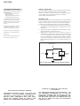
• All of the units included in the HT-CT180
(SA-CT180/SA-WCT180/Remote control)
are required to confirming operation
of SA-CT180. Check in advance that
you have all of the units.
Photo: SA-CT180
Note:
Be sure to keep your PC used for service and
checking of this unit always updated with the
latest version of your anti-virus software.
In case a virus affected unit was found during
service, contact your Service Headquarters.
COMPONENT MODEL NAME
HT-CT180
Bar Speaker (Active Speaker System)
Subwoofer (Active Subwoofer)
SA-CT180
SA-WCT180
• Please refer to service manual separately issued for Subwoofer.
SPECIFICATIONS
BLUETOOTH section
Amplifier section
U.S. models:
POWER OUTPUT AND TOTAL HARMONIC
DISTORTION:
(FTC)
Front L + Front R:
With 4 ohms loads, both channels
driven, from 200 Hz - 20,000 Hz; rated
13 Watts per channel minimum RMS
power, with no more than 1% total
harmonic distortion from
250 milliwatts to rated output.
POWER OUTPUT (reference)
Front L/Front R speaker:
25 Watts (per channel at 4 ohms,
1 kHz)
Except US models:
POWER OUTPUT (rated)
Front L + Front R:
13 W + 13 W (at 4 ohms, 1 kHz, 1% THD)
POWER OUTPUT (reference)
Front L/Front R speaker:
25 Watts (per channel at 4 ohms,
1 kHz)
Communication system
BLUETOOTH Specification version 4.0
Output
BLUETOOTH Specification Power Class
2
Maximum communication range
Line of sight approx. 10 m (33 ft) 1)
Maximum number of devices to be
registered
8 devices
Frequency band
2.4 GHz band (2.4000 GHz 2.4835 GHz)
Modulation method
FHSS (Freq Hopping Spread Spectrum)
Compatible BLUETOOTH profiles 2)
A2DP (Advanced Audio Distribution
Profile)
Supported Codecs 3)
SBC 4)
Transmission range (A2DP)
20 Hz - 20,000 Hz (Sampling frequency
44.1 kHz)
Inputs
OPTICAL
ANALOG
1)
The actual range will vary depending on
factors such as obstacles between
devices, magnetic fields around a
microwave oven, static electricity,
cordless phone, reception sensitivity,
operating system, software application,
etc.
2)
BLUETOOTH standard profiles indicate
the purpose of BLUETOOTH
communication between devices.
3)
Codec: Audio signal compression and
conversion format
4) Subband Codec
Speakers
Front L/Front R speaker section
Speaker system
2-way speaker system, Acoustic
suspension
Speaker
Tweeter: 14 mm - 25 mm ( 9 / 16 in - 1 in)
balance dome type
Woofer: 40 mm × 120 mm (1 5 / 8 in ×
4 3/ 4 in) cone type
General
Power requirements
120 V AC, 60 Hz (US and Canadian models)
220 V - 240 V AC, 50 Hz/60 Hz
(AEP, UK and Australian models)
Power consumption
On: 17 W
Standby mode: 0.5 W or less
BLUETOOTH Standby mode: 3 W or
less
Dimensions (approx.) (w/h/d)
901 mm × 52 mm × 84 mm
(35 1/ 2 in × 2 1/ 8 in × 3 3/ 8 in)
Mass (approx.)
2 kg (4 lb 7 oz)
Wireless transmitter
Frequency band
2.4 GHz band (2.404 GHz - 2.476 GHz)
Modulation method
GFSK
Supplied accessories
Remote control (1)
R03 (size AAA) batteries (2)
Optical digital cable (1)
Speaker pads for the subwoofer (4)
Design and specifications are subject to
change without notice.
HT-CT180
SOUND BAR
SA-CT180
ACTIVE SPEAKER SYSTEM
9-896-127-01
2015B33-1
© 2015.02
Sony Corporation
Published by Sony Techno Create Corporation
HT-CT180
Copyrights and Trademarks
This system incorporates Dolby* Digital
Surround System.
* Manufactured under license from
Dolby Laboratories.
Dolby, and the double-D symbol are
trademarks of Dolby Laboratories.
The BLUETOOTH® word mark and logos
are registered trademarks owned by
Bluetooth SIG, Inc. and any use of such
marks by Sony Corporation is under
license.
The N Mark is a trademark or registered
trademark of NFC Forum, Inc. in the
United States and in other countries.
Android™ is a trademark of Google Inc.
“ClearAudio+” is a trademark of Sony
Corporation.
Other trademarks and trade names are
those of their respective owners.
SAFETY CHECK-OUT
After correcting the original service problem, perform the following safety check before releasing the set to the customer:
Check the antenna terminals, metal trim, “metallized” knobs,
screws, and all other exposed metal parts for AC leakage.
Check leakage as described below.
LEAKAGE TEST
The AC leakage from any exposed metal part to earth ground and
from all exposed metal parts to any exposed metal part having a
return to chassis, must not exceed 0.5 mA (500 microamperes.).
Leakage current can be measured by any one of three methods.
1. A commercial leakage tester, such as the Simpson 229 or RCA
WT-540A. Follow the manufacturers’ instructions to use these
instruments.
2. A battery-operated AC milliammeter. The Data Precision 245
digital multimeter is suitable for this job.
3. Measuring the voltage drop across a resistor by means of a
VOM or battery-operated AC voltmeter. The “limit” indication
is 0.75 V, so analog meters must have an accurate low-voltage
scale. The Simpson 250 and Sanwa SH-63Trd are examples
of a passive VOM that is suitable. Nearly all battery operated
digital multimeters that have a 2 V AC range are suitable. (See
Fig. A)
To Exposed Metal
Parts on Set
0.15 μF
1.5 kΩ
AC
voltmeter
(0.75 V)
Earth Ground
Fig. A. Using an AC voltmeter to check AC leakage.
SAFETY-RELATED COMPONENT WARNING!
COMPONENTS IDENTIFIED BY MARK 0 OR DOTTED LINE
WITH MARK 0 ON THE SCHEMATIC DIAGRAMS AND IN
THE PARTS LIST ARE CRITICAL TO SAFE OPERATION.
REPLACE THESE COMPONENTS WITH SONY PARTS
WHOSE PART NUMBERS APPEAR AS SHOWN IN THIS
MANUAL OR IN SUPPLEMENTS PUBLISHED BY SONY.
2
ATTENTION AU COMPOSANT AYANT RAPPORT
À LA SÉCURITÉ!
LES COMPOSANTS IDENTIFIÉS PAR UNE MARQUE 0 SUR
LES DIAGRAMMES SCHÉMATIQUES ET LA LISTE DES
PIÈCES SONT CRITIQUES POUR LA SÉCURITÉ DE FONCTIONNEMENT. NE REMPLACER CES COMPOSANTS QUE
PAR DES PIÈCES SONY DONT LES NUMÉROS SONT DONNÉS DANS CE MANUEL OU DANS LES SUPPLÉMENTS
PUBLIÉS PAR SONY.
HT-CT180
SECTION 1
SERVICING NOTES
TABLE OF CONTENTS
1.
SERVICING NOTES .............................................
3
2.
DISASSEMBLY
2-1.
2-2.
2-3.
2-4.
2-5.
2-6.
2-7.
2-8.
2-9.
2-10.
2-11.
Disassembly Flow ...........................................................
Rear Cabinet Block .........................................................
AC Cord (AC1) ...............................................................
MAIN Board Block ........................................................
MAIN Board ...................................................................
NFC Module ...................................................................
LED Board ......................................................................
Antenna (ANT1) .............................................................
Loudspeaker (SP1, SP3) (L-ch) ......................................
BT NFC Board ................................................................
Loudspeaker (SP2, SP4) (R-ch) ......................................
3.
TEST MODE ............................................................ 16
4.
DIAGRAMS
4-1.
4-2.
4-3.
4-4.
4-5.
4-6.
4-7.
4-8.
4-9.
4-10.
4-11.
4-12.
4-13.
4-14.
Block Diagram ................................................................
Printed Wiring Board - MAIN Board - ...........................
Schematic Diagram - MAIN Board (1/6) - .....................
Schematic Diagram - MAIN Board (2/6) - .....................
Schematic Diagram - MAIN Board (3/6) - .....................
Schematic Diagram - MAIN Board (4/6) - .....................
Schematic Diagram - MAIN Board (5/6) - .....................
Schematic Diagram - MAIN Board (6/6) - .....................
Printed Wiring Board - KEY Board -..............................
Schematic Diagram - KEY Board - ................................
Schematic Diagram - BT NFC Board -...........................
Printed Wiring Board - BT NFC Board - ........................
Printed Wiring Board - LED Board - ..............................
Schematic Diagram - LED Board -.................................
5.
EXPLODED VIEWS
6
7
8
9
10
11
11
12
13
14
15
17
19
20
21
22
23
24
25
25
25
26
27
27
27
5-1. Rear Cabinet Section ...................................................... 32
5-2. Front Cabinet Section ..................................................... 33
6.
ACCESSORIES ....................................................... 34
The SERVICING NOTES contains important information for
servicing. Be sure to read this section before repairing the
unit.
UNLEADED SOLDER
Boards requiring use of unleaded solder are printed with the leadfree mark (LF) indicating the solder contains no lead.
(Caution: Some printed circuit boards may not come printed with
the lead free mark due to their particular size)
: LEAD FREE MARK
Unleaded solder has the following characteristics.
• Unleaded solder melts at a temperature about 40 °C higher
than ordinary solder.
Ordinary soldering irons can be used but the iron tip has to be
applied to the solder joint for a slightly longer time.
Soldering irons using a temperature regulator should be set to
about 350 °C.
Caution: The printed pattern (copper foil) may peel away if
the heated tip is applied for too long, so be careful!
• Strong viscosity
Unleaded solder is more viscous (sticky, less prone to flow)
than ordinary solder so use caution not to let solder bridges
occur such as on IC pins, etc.
• Usable with ordinary solder
It is best to use only unleaded solder but unleaded solder may
also be added to ordinary solder.
ADVANCE PREPARATION WHEN CONFIRMING OPERATION
All of the units included in the HT-CT180 (SA-CT180/SAWCT180/Remote control) are required to confirming operation of
SA-CT180. Check in advance that you have all of the units.
DESTINATION ABBREVIATIONS
The following abbreviations for model destinations are used in this
service manual.
• Abbreviations
AUS : Australian model
CND : Canadian model
3
HT-CT180
MODEL IDENTIFICATION
Distinguish by Part No. on the bottom side of a main unit.
Note: The printed contents of following figure model number label may be different from the model number label of a main unit.
MODEL NUMBER LABEL
US and Canadian models
4-559-553-0[]
AEP model
4-559-554-0[]
UK model
4-559-555-0[]
Australian model
4-562-621-0[]
– Bottom view –
4
HT-CT180
ABOUT PARTS REPAIR OF EACH BOARDS
When each boards installed in this unit are defective, individual
electrical parts that the mount is done cannot be replaced. When
each boards are defective, replace the mounted board or the whole
parts including an applicable board.
Printed wiring board and schematic diagram that have been described on this service manual are for reference.
(Printed wiring board and schematic diagram of WIERLESS board
have not described)
NOTE OF REPLACING THE BT NFC BOARD OR THE
NFC MODULE
When replacing the BT NFC board or the NFC module, be sure to
replace both at the same time.
The BT NFC board or the NFC module cannot replace with single.
METHOD OF RESET
If the system still does not operate
properly, reset the system as follows:
1
2
While holding down the @/1 (on/
standby) button on the system,
hold down the INPUT and VOL –
buttons simultaneously for 5
seconds.
All 5 indicators on the Bar Speaker
flash 3 times, and the settings
return to their initial status.
Disconnect the AC power cord
(mains lead).
WHAT TO DO IF PROTECT
If all of the LEDs are lit, it is state in the protect. This state shows
an abnormality of the AMP circuit.
In this case, there is a possibility that the MAIN board is defective.
Please replace the MAIN board.
NOTE OF REPLACING THE WIRELESS BOARD
When replaced the WIRELESS board, link of SA-CT180 and SAWCT180 will be disconnected.
Before you return repaired unit to customers, please link the SACT180 and SA-WCT180 by the following procedure.
If, in a state in which only one of SA-CT180 or SA-WCT180 is
brought into service field, and replaced the WIRELESS board of
SA-CT180 or SA-WCT180, when returning the repaired unit, be
sure to inform the customers that it is necessary to link the following procedure.
Enabling the Secure Link
function
You can specify the wireless connection
to link the Bar Speaker to the subwoofer
using the Secure Link function. This
function can help prevent interference if
you use multiple wireless products or
your neighbors use wireless products.
1
2
Press LINK on the rear of the
subwoofer.
You will hear beeps from the
subwoofer.
Hold down PAIRING on the Bar
Speaker for 5 seconds, then VOL –
for 5 seconds.
The OPTICAL and ANALOG
indicators flash alternately.
When the Bar Speaker is linked to
the subwoofer, the indicators stop
flashing.
If it failed, the indicators light up for
5 seconds. Try again the above
operation.
5
HT-CT180
SECTION 2
DISASSEMBLY
•
This set can be disassembled in the order shown below.
2-1.
DISASSEMBLY FLOW
SET
2-2. REAR CABINET BLOCK
(Page 7)
2-3. AC CORD (AC1)
(Page 8)
2-4. MAIN BOARD BLOCK
(Page 9)
2-6. NFC MODULE
(Page 11)
2-5. MAIN BOARD
(Page 10)
2-7. LED BOARD
(Page 11)
2-10. BT NFC BOARD
(Page 14)
2-8. ANTENNA (ANT1)
(Page 12)
2-11. LOUDSPEAKER (SP2, SP4) (R-CH)
(Page 15)
2-9. LOUDSPEAKER (SP1, SP3) (L-CH)
(Page 13)
6
HT-CT180
Note: Follow the disassembly procedure in the numerical order given.
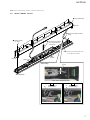
2-2.
REAR CABINET BLOCK
4 rear cabinet block
Right side
3 KEY board cable connector
(XP3)
1 thirteen screws
(3 u 10 B)
2 Lift up the rear cabinet
block in the direction
of the arrow.
Note: Please spread a sheet under a unit
not to injure front cabinet.
Left side
Top side
Bottom side
:LUHVHWWLQJ
groove
– Rear top view –
–5HDUFDELQHWEORFNIURQWYLHZ–
rib
wire
OK
The wire and rib
are separated.
rib
NG
The wire and rib
are overlapping.
wire
7
HT-CT180
2-3.
AC CORD (AC1)
cord bush
2 claw
2 claw
– Front cabinet rear view –
1 AC cord connector
(CN501)
Bottom side
Left side
Top side
4 AC cord block
Note 1: Please spread a sheet under a unit
not to injure front cabinet.
– Rear top view –
hole
7 AC cord (AC1)
3 Draw the AC cord block
out of the hole in rear
cabinet block.
5 claw
6 cord bush
How to install the cord bush
Note 2: When installing the cord bush to the AC cord (AC1),
check the directions of the white line of the AC cord (AC1)
and the claw of the cord bush, and install correctly.
AC cord (AC1)
[white line]
claw
cord bush
Installation direction for the cord bush
cord bush
claw
65 ± 5 mm
Note 3: Make sure that the white line is at the bottom.
– Front cabinet rear view –
8
HT-CT180
2-4.
MAIN BOARD BLOCK
7 antenna wire terminal
3 two screws
(3 u 8 S)
Right side
5 FFC 22P (FFC2)
(XS1)
9 MAIN board block
6 R-ch speaker cable connector
(XP11)
8 L-ch speaker cable connector
(XP10)
2 NFC cable
connector
(XP12)
Bottom side
1 FFC 10P (FFC1)
(XP20)
Top side
4 Lift up the MAIN board
block in the direction
of the arrow.
Left side
–)URQWFDELQHWEORFNUHDUWRSYLHZ–
front side
Install the antenna wire
straight from the front side.
groove
groove
groove
connector
colored line
connector
:LUHVHWWLQJ
FFC 22P (FFC2)
OK
Insert straight into the interior.
flexible flat
cable
colored line
NG
Insert at a slant.
flexible flat
cable
Note: Please spread a sheet under a unit
not to injure front cabinet.
speaker wire
How to install the flexible flat cable
When installing the flexible flat cable,
ensure that the colored line is parallel
to the connector after insertion.
speaker wire
WIRELESS board
–)URQWFDELQHWEORFNUHDUYLHZ–
NG
OK
The FFC is goes around the parts.
–7RSYLHZ–
FFC 10P (FFC1)
The FFC goes in between the parts.
–7RSYLHZ–
FFC 10P (FFC1)
9
HT-CT180
2-5.
MAIN BOARD
2 WIRELESS board
Note 1: When WIRELESS board is replaced, refer to
“NOTE OF REPLACING THE WIRELESS
BOARD” on page 5.
4 cushion (A)
(See Fig. A)
7 four screws
(3 u 6 B)
5 cushion (B)
(See Fig. A)
0 MAIN board
6 cushion (EVA)
(See Fig. B)
1 connector
(XP7)
7 two screws
(3 u 6 B)
3 cushion (C)
(See Fig. A)
9 sheet (IC)
(See Fig. C)
8 Remove the MAIN board block
in the direction of the arrow.
3 cushion (C)
(See Fig. A)
–0$,1ERDUGEORFNIURQWYLHZ–
3DVWLQJSRVLWLRQRIFXVKLRQV
Note 2: When replacing the MAIN board, make sure to affix these cushions and the sheet.
The cushions and the sheet are supplied as a set.
< Fig. A>
cushion (C)
MAIN board
MAIN board
screw
(3 u 6 B)
1 ± 0.5 mm
MAIN board
cushion (C)
cushion (A)
1 ± 0.5 mm
guide line
cushion (B)
MAIN board –7RSYLHZ– cushion (B)
cushion (C)
cushion (B)
cushion (A)
guide line
cushion (C)
–0$,1ERDUGEORFNUHDUYLHZ–
< Fig. B>
< Fig. C>
sheet (IC)
IR602
guide line
guide line
cushion (EVA)
MAIN board
guide line
–)URQWYLHZ–
10
cushion (EVA)
metal panel
–0HWDOSDQHOWRSYLHZ–
HT-CT180
2-6.
NFC MODULE
Note 1: When replacing the BT NFC board or the NFC module, be sure to
replace both at the same time.
The BT NFC board or the NFC module cannot replace with single.
2 screw
(3 u 8 S)
1 connector
(XP12)
5 NFC module
4 NFC bracket
+RZWRLQVWDOOWKH1)&PRGXOH
Note 3: When installing the NFC module
to the NFC bracket, install so that
the solder portion of the wire is
positioned as shown in the figure
below.
3 Peel off the adhesive sheet.
NFC bracket
solder portion
Bottom side
Left side
Note 2: Please spread a sheet
under a unit not to
injure front cabinet.
Top side
– Front cabinet block rear top view –
2-7.
NFC module
– NFC module block bottom view –
LED BOARD
1 FFC 10P (FFC1)
(XP5)
How to install the flexible flat cable
When installing the flexible flat cable,
ensure that the colored line is parallel
to the connector after insertion.
terminal side
2 two screws
(3 u 8 S)
Right side
3 LED board
OK
Insert straight into the interior.
flexible flat
cable
colored line
connector
NG
Insert at a slant.
flexible flat
cable
colored line
connector
Note: Please spread a sheet under a unit
not to injure front cabinet.
Bottom side
– Front cabinet block rear bottom view –
Left side
11
HT-CT180
2-8.
ANTENNA (ANT1)
:LUHVHWWLQJ
three grooves
three grooves
antenna wire
groove
Note 2: Pass the antenna wire between the loudspeaker
and the front cabinet block.
woofer
(L-ch)
tweeter
(L-ch)
Right side
1 Peel off the
adhesive sheet.
Note 1: Please spread a sheet under a unit
not to injure front cabinet.
2 antenna
(ANT1)
Bottom side
Left side
–)URQWFDELQHWEORFNUHDUERWWRPYLHZ–
12
HT-CT180
2-9.
LOUDSPEAKER (SP1, SP3) (L-CH)
6SHDNHUFRUGVHWWLQJ/FK
terminal
(wide side)
[red]
Note 2: Pass the speaker cord
over the top of the
loudspeaker (SP2).
terminal
(narrow side)
[black]
2 speaker cord
1 terminal
(narrow side)
[black]
1 terminal
(wide side)
[red]
3 four screws
(3 u 8 S)
loudspeaker
(SP1)
4 loudspeaker
(4.3 u 12 cm)
(SP1)
terminal
(narrow side)
[black]
terminal
(wide side)
[red]
loudspeaker
(SP3)
1 terminal
(narrow side)
[black]
5 screw
(2.6 u 8 S)
1 terminal (wide side)
[red]
5 screw
(2.6 u 8 S)
6 loudspeaker
(1.4 u 2.5 cm)
(SP3)
Right side
Note 1: Please spread a sheet under a unit
not to injure front cabinet.
Bottom side
– Front cabinet block rear bottom view –
Left side
,QVWDOODWLRQGLUHFWLRQIRUWKHORXGVSHDNHU4.3 × 12 FP63
terminal (wide side)
[red]
top side
terminal (narrow side)
[white]
How to install the speaker terminal
Insert the speaker terminal straight into the interior.
There is a possibility that using this unit without the
speaker terminal correctly installed will damage it.
OK
Insert straight into the interior.
speaker cord speaker terminal
loudspeaker
(SP1)
– Front cabinet block rear view –
NG
nsert only part way.
speaker cord speaker terminal
13
HT-CT180
2-10. BT NFC BOARD
Note 1: When replacing the BT NFC board or the NFC module, be sure to
replace both at the same time.
The BT NFC board or the NFC module cannot replace with single.
:LUHVHWWLQJ
Right side
Top side
tweeter
(R-ch)
BT NFC board
Bottom side
+RZWRLQVWDOOWKHIOH[LEOHIODWFDEOH
When installing the flexible flat cable,
ensure that the colored line is parallel
to the connector after insertion.
Note 3: Pass the FFC 22P (FFC2) between
the loudspeaker and the front cabinet block.
Left side
2 FFC 22P (FFC2)
(XP19)
terminal
side
Left side
3 BT NFC board
NG
Insert at a slant.
flexible flat
cable
Bottom side
colored line
connector
Note 2: Please spread a sheet under a unit
not to injure front cabinet.
Right side
–)URQWFDELQHWEORFNUHDUERWWRPYLHZ–
14
FFC 22P (FFC2)
1 Remove the BT NFC board block
straightly in the direction of the arrow.
OK
Insert straight into the interior.
flexible flat
cable
colored line
connector
woofer
(R-ch)
HT-CT180
2-11. LOUDSPEAKER (SP2, SP4) (R-CH)
6SHDNHUFRUGVHWWLQJ5FK
terminal
(narrow side)
[black]
loudspeaker
(SP4)
terminal
(narrow side)
[black]
terminal
(wide side)
[red]
Note 2: Pass the speaker cord
over the top of the
loudspeaker (SP2).
loudspeaker
(SP2)
terminal
(wide side)
[red]
+RZWRLQVWDOOWKHVSHDNHUWHUPLQDO
Insert the speaker terminal straight into the interior.
There is a possibility that using this unit without the
speaker terminal correctly installed will damage it.
OK
Insert straight into the interior.
speaker cord speaker terminal
2 speaker cord
1 terminal (wide side)
[red]
3 screw
(3 u 8 S)
1 terminal (narrow side)
[black]
3 three screws
(3 u 8 S)
1 terminal
(narrow side)
[black]
4 loudspeaker
(4.3 u 12 cm)
(SP2)
NG
nsert only part way.
speaker cord speaker terminal
1 terminal
(wide side)
[red]
5 screw
(2.6 u 8 S)
5 screw
(2.6 u 8 S)
Left side
6 loudspeaker
(1.4 u 2.5 cm)
(SP4)
Note 1: Please spread a sheet under a unit
not to injure front cabinet.
,QVWDOODWLRQGLUHFWLRQIRUWKHORXGVSHDNHU×FP63
top side
Right side
Bottom side
terminal (narrow side)
[white]
terminal (wide side)
[red]
–)URQWFDELQHWEORFNUHDUERWWRPYLHZ–
loudspeaker
(SP2)
–)URQWFDELQHWEORFNUHDUYLHZ–
15
HT-CT180
SECTION 3
TEST MODE
VERSION DISPLAY
The check of the software version can be performed.
Procedure:
1. Press the [@/1] button to turn the power on.
2. Press three buttons of the [INPUT], [VOL+] and [VOL−] simultaneously for 2 seconds.
3. When enter the version display mode, the software version is
shown by the frequency of blinking of each LED.
LED showing the software version
DEMO MODE
The demo mode can be performed.
(This mode is used by shop front)
Procedure:
1. Press the [@/1] button to turn the power on.
2. Press two buttons of the [INPUT] and [VOL−] simultaneously
for 5 seconds.
3. When enter the demo mode, ANALOG function LED is blink
twice quickly, then changed to the setting of initial value for
demo mode.
blink twice quickly
Software version
X.XX
Minor version (Lower) (BLUETOOTH function LED)
Minor version (Upper) (ANALOG function LED)
Major version (OPTICAL function LED)
Example: When the software version is “1.02”
OPTICAL function LED is blink once.
ANALOG function LED is not blink.
BLUETOOTH function LED is blink twice.
4. When the version display is finished, return to the normal
mode.
FACTORY RESET
It can clear all settings and the Bluetooth pairing history to initial
conditions. Execute this mode when returning this unit to the customer.
Procedure:
1. Press the [@/1] button to turn the power on.
2. Press three buttons of the [INPUT], [VOL−] and [@/1] simultaneously for 5 seconds.
3. Blink three times all LEDs, then lights up all LEDs. When the
reset is complete, all LEDs light off and becomes the standby
status.
16
Initial value for demo mode:
Function
: OPTICAL
Volume
: 25
Muting
: OFF
Sound field
: CLEAR AUDIO+
Night mode
: OFF
Voice
: OFF
Subwoofer volume : 10
Dual mono
: MAIN
Note 1: When demo mode is “ON”, the operation of the [@/1] button on
the unit, and the operation of the [@/1] and [INPUT] buttons on
the remote commander is invalid.
Note 2: When the non-operation and no sound for five minutes is followed, setting will return to the initial value for demo mode.
Releasing method:
Perform the “FACTORY RESET”.
Note: The demo mode does not release by unplug the AC cord.
HT-CT180
SECTION 4
DIAGRAMS
4-1.
BLOCK DIAGRAM
Wireless Module
IA2S4M
Optical In
AUDIO_IN
ADC
AK5358
TAS3157*2
TBMC830
DATA3
MCLK
BCLK
LRCLK
I/O
BCLK1
MCLK LRCLK1
I/O
NFC
NFC-FS2
SPI FLASH
16M
DATA0
MTK8301
BTL
IIC2
REST
BCLK2
LRCLK2
DATA1
4ɏ 25W THD 30%
Audio
Processor
STA339BW
IIC1
SPI1
BTL
SDRAM
IR
27M
01U0IRR
CV-102
crystall
DC-DC
16.5V
STB_3.3V
STB 3 3V
STB_3.3V
16.5V
DC-DC
EUP3482A
16.5V
HT-CT180
5V
For IA2S4M
ˈAK5358,
TAS3157*2,
F4558*1,
power
LED *5
5
signal
)RUMTK8301Ƚ)ODVKȽSDRAMǃIRǃ
NFCǃ TBM-C830
EUP3482A
POWER
SUPPLY
KEY *5
5
STB_3.3V
4ɏ 25W THD 30%
LDO
CW1117
Switch
G9012M
1 25V
1.25V
3.3V
)RU 67$%:
)RU67$%:
17
17
)RU07.
)RU67$%:Ƚ/('
Ƚ237
HT-CT180
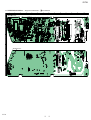
THIS NOTE IS COMMON FOR PRINTED WIRING BOARDS AND SCHEMATIC DIAGRAMS.
(In addition to this, the necessary note is printed in each block.)
For Printed Wiring Boards.
For Schematic Diagrams.
Note:
•
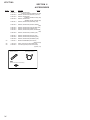
: Pattern from the side which enables seeing.
(The other layers’ patterns are not indicated.)
Note:
• All capacitors are in μF unless otherwise noted. (p: pF) 50
WV or less are not indicated except for electrolytics and
tantalums.
• All resistors are in Ω and 1/4 W or less unless otherwise
specified.
Caution:
Pattern face side:
(Conductor Side)
Parts face side:
(Component Side)
Parts on the pattern face side seen
from the pattern face are indicated.
Parts on the parts face side seen from
the parts face are indicated.
Note:
The components identified by mark 0 or dotted
line with mark 0 are critical for safety.
Replace only with part
number specified.
• Circuit Boards Location
LED board
Note:
Les composants identifiés
par une marque 0 sont
critiques pour la sécurité.
Ne les remplacer que par
une pièce portant le numéro spécifié.
NFC module
WIRELESS board
MAIN board
BT NFC board
KEY board
HT-CT180
18
18
HT-CT180
4-2.
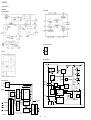
PRINTED WIRING BOARD - MAIN Board 1
2
3
• See page 18 for Circuit Boards Location.
4
5
6
•
: Uses unleaded solder.
7
8
MAIN BOARD (COMPONENT SIDE)
A
B
C
D
MAIN BOARD (CONDUCTOR SIDE)
E
F
HT-CT180
19
19
9
10
11
12
13
14
HT-CT180
SCHEMATIC DIAGRAM - MAIN Board (1/6) -
1
3
4
5
6
7
8
MAIN BOARD (1/6)
HV
1M
LIF501
2
1M
RV501
CN501
FB502
2PIN/7.92mm
F501
T3.15AL250V
TR501
FB90@100MHz
CE502
4 -
VDR/620VR502B R502D
470pF/250VAC
CY501
1M 1M
+
+ 1
82uF/450V
3
1
2
1
2
KBP306
BD1
LIF4-22-15
470pF/250VAC
CY502
2
FB504
FB90@100MHz
R502C
4
R502A
1
A
2
• See page 28 for IC Block Diagrams.
3
4-3.
C537
NC/1500pF/1KV
FB501
CX501
FB90@100MHz
NTC/3ohm/5A
0.33uF/250VAC
B
CY507
HV
220pF/250VAC
CY506
220pF/250VAC
C533
1500pF/1KV
R569 0
R570 0
T502
EF25
HV
VDD
1
VDD
D533
A9
A122
MUR420/4A/200V
8
9
C531
1500pF/1KV
C
MUR420/4A/200V
3
R572
R565
22
2M
R571
150K
+
R566
22
D
7
R510
NC
U531
D
D
A12
A13
11
12
6
ZD536
NC
V
R544
68.1K/1%
P-GND
R541
1.5K
0.1uF/50V/X7R
CE532
+
ZD535
47uF/35V
100
NC/BZX79C27
* CAUTION :
ARE IMPORTANT PARTS ON THE SAFETY.
PLEASE USE THE PARTS HAVING THE DESIGNATED PARTS NUMBER WITHOUT FAIL.
HT-CT180
20
20
C534
0.1uF/50V/X7R
U533
1
ZD531
BZX79C12
3
R533
0
R543 100K
2
3
CE531
+
47uF/35V
C532
C535 220pF/50V/X7R
U532
LTV-817S
R539
E
R542
3.3K
R538
5.6
4
X F
C549
0.1uF/50V/X7R
FR104/1A/400V
C
100pF/1KV
THE PARTS MARKED WITH
+
GND
FB
R540 D532
15
C536
F
CE533
470uF/35V
FB
CONTROL
TOP256EN S
4
CE535
470uF/25V
D531
FR207/2A/1000V
R537
2M
D
R567
150K
R568
150K
2
150K
N.C
1
R536
+18V
AS431
R557
12.1k/1%
R546
100K
ZD533
NC
HT-CT180
4-4.
SCHEMATIC DIAGRAM - MAIN Board (2/6) -
1
A
2
• See page 28 for IC Block Diagrams.
3
4
5
6
7
8
MAIN BOARD (2/6)
STB_3V3
R3
10K
POWER_18V
Vout=0.923(R1+R2/R2)
600/2A
input
Vout
FB
EUP3482ADIR1
3
5
100pF
FB=0.923V
C11
3300pF//50V/X7R
C152
R10
150 ohm
39.2K/1%
CE25
+
C236
SW
R96
7.5K/1%
R97
7.5K/1%
7.5K
2
4
1
NC/10uF/10V/X7R
0.1uF/25V/Y5V
R19
C80
NC/120/1%
10uF/10V/X7R
1uF
1.25V
C24
C79
Out
0
0.1uF
SS
NC
EN
100UF/25V
22K
8
D542
C7
1V2
R18
C23
C199 4.7uF/16V/Y5V
ADJ/GND
3
R16
10uH/2A
10uF/10V/X7R
C
L1
1
2
7
R6
0.1uF/25V/Y5V
U4
AS1117
0.01uF
R57
C10
STB_3V3
STB_3V3
R99
IN
220uF35V
C6
U2
C75
330pF/50V/NP0
NC/0.1uF
1uF/50V/X7R
56
C4
C200
+
BS
C3
R5
47K
COMP
10K
R1
CE7
GND
FB19
0.1uF/25V/Y5V
4
POWER_ON
0.1uF
10K
C12
C234
R9
B
Rate : 2A 30V 160m 340KHz
In Range: 4-30V
Out Range: 0.923V-12V
0.1uF
R8
AMP_VCC
TP43
Close to U2_EUP3482A
Q1
NPN_3DG3904M
EN2
6
POWER_18V
EN2
C16 0.01uF
HT-CT180
R21
560
0.1uF/25V/Y5V
C25
EN2
0.1uF/25V/Y5V
R81
100pF
FB=0.923V
3300pF//50V/X7R
C162
R95
150 ohm
CE27
+
51K/1%
C255
D543
5
R120
1K/1%
R121
7.5K
21
10K/1%
0.1uF
3
100UF/25V
C19
NC
1
BS
COMP
FB
6
IN
GND
2
21
SW
SS
4
0.1uF
100
EN
EUP3482ADIR1
0.1uF/25V/Y5V
E
22K
8
C18
C755
POWER_ON
R122
10uH/1A
R123
10uF/10V/X7R
7
C20
Q3
PNP_3CG9012M
R774
L2
R115
U3
C82
330pF/50V/NP0
10UF/25V/X7R
10UF/25V/X7R
SYS_3V3
C17
SYS_5V
C237
56
STB_3V3
Vout=0.923(R1+R2/R2)
C15
0.1uF
D
Close to U2_EUP3482A
0
R25
C116
0
HT-CT180
SCHEMATIC DIAGRAM - MAIN Board (3/6) -
1
2
3
4
5
7
8
9
MAIN BOARD (3/6)
A_1V2
A_1V2
Mute
AMP_FAULT
AMP_SCL
AMP_SDA
LED3
LED4
LED1
LED4
MTK_DATA1
A_3V3
TX2+
A_3V3
R202
R201
SUB_SDA
SUB_SCL
A_3V3
33
33
33
33
129
E-PAD/GND
MTK_DATA0 R59
MTK_DATA1 R61
D_1V2
TX1+
TX1-
TXC+
TXCR51
0
R52
1.5K/1%
R53
D_1V2
R82
D_1V2
M_A3
M_A2
M_A1
M_A0
M_A10
BA1
BA0
D_3V3
RAS
CAS
RWE
M_A4
M_A5
M_A6
1K
BT_Pairing
POWER_ON
10K
D_3V3
M_A7
M_A8
22pF/50V/NP0
SDCLK
AMP_RST1
Mute
R73
R74
R75
R76
10PF/50V/NP0
10PF/50V/NP0
4
C61
2
33
33
33
33
AMCLK
ABCLK
ALRCLK
ADATA
AMCLK
ABCLK
ALRCLK
ADATA
4.7K
SUB_SDA
SUB_SCL
SUB_IIC_BUSY
22
22
R119
1/2power_control
AMP_FAULT
R125
AMP_SCL
AMP_SDA
33
AMP_RST
Mute
NC/33
1/2power-control
AMP_FAULT
R101
4.7K
SUB_SDA
SUB_SCL
SUB_IIC_BUSY
TP1
TXC+
TXC+
TP2
TXC-
TXC-
TP3
TX0+
TX0+
TX0-
TX0-
TX1+
TX1+
TX1-
TX1-
TP4
TP5
TP6
TX2+
TP7
TX2-
TP8
TP9
TP10
NC/0
HT-CT180
C62
Put these Compnonents as
closer as possible to
MT8307
R90
4.7K
SF_3V3
SF_CK
R28
0
SF_DI
R30
0.1uF/25V/Y5V
8
CE# VDD 7
SO HOLD# 6
WP# SCK 5
VSS
SI
SPI_16Mb_EN25T160
C64
10PF/50V/NPO
4.7K
4.7K
0.1uF/25V/Y5V
XO
AMP_SCL
AMP_SDA
AMP_SCL
AMP_SDA
10PF/50V/NP0
R88
R89
C65
F
C66
U7
33
27pF/50V/NP0
SF_3V3
1
2
3
4
R84
C63
0
SF_CS
SF_DO
1
BT_RESET
BT_STATUS2
BT_FN
BT_POWER_CONTROL
BT_PIO7
BT_STATUS1
TP12 TP13
33
C59
25mA
27pF/50V/NP0
R34
SF_3V3
IR
NFC_INT
MP3_BT_SW
R72
C60
STB_3V3
LED3
LED1
BT_RESET
BT_STATUS2
BT_FN
BT_POWER_CONTROL
BT_PIO7
BT_STATUS1
AD_MCLK
AD_BCLK
AD_LRCK
AD_DATA
1M
VOL+
VOLFUNCTION
LED3
LED1
NFC_INT
MP3_BT_SW
E
3
10K
VOL+
VOL-
IR
R94
R83
AMP_DATA0
AMP_DATA1
R381 R380
SYS_3V3
XI
AMP_DATA0
AMP_DATA1
33
33
SYS_3V3
M_A11
M_A9
DQ13
DQ12
DQ11
DQ10
DQ9
DQ8
UDQM
DQ0
DQ1
DQ2
DQ3
DQ4
DQ5
DQ6
DQ7
LDQM
DQ15
DQ14
D_3V3
4PIN/2.0mm
SDCLK
SD_3V3
M_A11
M_A9
M_A8
M_A7
M_A6
M_A5
M_A4
D_3V3
1K/1%
MT8301_OQE
LQFP128-630630-0.4-88D5100
C72
TP18
UDQM
SD_CLK
R42
4.7K
R370
10K
TX0+
TX0-
DV_C1
DV_C2
DV_C3
SD_MS_D2
SD_MS_D3
GPIO13
GPIO9
GPIO8
GPIO7/CKE_
DVDD33
RD0
RD1
RD2
RD3
RD4
RD5
RD6
RD7
DQM0
RD15
RD14
DVDD12
RD13
RD12
RD11
RD10
RD9
RD8
DQM1
RCLK
RA11
RA9
33
34
35
36
37
38
39
40
41
42
43
44
45
46
47
48
49
50
51
52
53
54
55
56
57
58
59
60
61
62
63
64
BT_RESET
BT_STATUS2
BT_POWER_CONTROL
BT_PIO7
33
R93
AMP_RST1
BT_STATUS1
BT_FN
MP3_BT_SW
NC/0.1uF/25V/Y5V
1
2
3
4
SD_3V3
DQ8
NC/15pF/50V/NP0
DSP_RXD
DSP_TXD
XP2
DQ10
DQ9
C33
1
2
3
4
SD_3V3
DQ12
DQ11
10PF/50V/NP0
TP14TP15TP16 TP17
STB_3V3
DQ14
DQ13
10PF/50V/NP0
STB_3V3
DQ15
C50
10K
54
53
52
51
50
49
48
47
46
45
44
43
42
41
40
39
38
37
36
35
34
33
32
31
30
29
28
C51
10K
STB_3V3
100pF/50V/NP0
R371 R369
R64
100pF/50V/NP0
0.1uF/25V/Y5V
R63
1K
1K
4.7K
C273
0.1uF/25V/Y5V
4.7K
33
VSS
DQ15
VSSQ
DQ14
DQ13
VDDQ
DQ12
DQ11
VSSQ
DQ10
DQ9
VDDQ
DQ8
VSS
NC
UDQM
CLK
CKE
NC
A11
A9
A8
A7
A6
A5
A4
VSS
C77 0.1uF/25V/Y5V
IR
R70
NFC_INT
R963
FUNCTION
R962
POWER
V1.0
U5
VDD
DQ0
VDDQ
DQ1
DQ2
VSSQ
DQ3
DQ4
VDDQ
DQ5
DQ6
VSSQ
DQ7
VDD
LDQM
WE
CAS
RAS
CS
BA0
BA1
A10/AP
A0
A1
A2
A3
VDD
SYS_3V3
TX2-
0.1uF/25V/Y5V
1.2K/1%
1.2K/1%
C274
C58
0.1uF/25V/Y5V
0.1uF/25V/Y5V
C57
500/500mA
C78
C56
0.1uF/25V/Y5V
0.1uF/25V/Y5V
0.1uF/25V/Y5V
C54
4.7uF/16V/Y5V
C55
FB8
R67
R68
LQFP 128
96
95
94
93
92
91
90
89
88
87
86
85
84
83
82
81
80
79
78
77
76
75
74
73
72
71
70
69
68
67
66
65
4.7uF/16V/Y5V
1K
SF_CK
TX2N
AVDD12_D
TX1P
TX1N
AVSS12
TX0P
TX0N
AVDD12_C
TXCP
TXCN
AVDD33_12
EXT_RES
GPIO10/HPLG
SPDIF/GPIO12
DVDD12
RA3
RA2
RA1
RA0
RA10
BA1
BA0
DVDD33
RAS_
CAS_
RWE_
RA4
RA5
RA6
DVDD33
RA7
RA8
MT8307
1
2
3
4
5
6
7
8
9
10
11
12
13
14
15
16
17
18
19
20
21
22
23
24
25
26
27
SDRAM_64Mb_M12L64164A-7T
C44
D_3V3
AVDD12_2
AVDD33_1
XTALI
XTALO
V14
GPO5
AVDD33_2
NC
NC
GPIO2
USB_DP
USB_DM
VDD33_USB
PAD_VRT
VDD12_USB
DV_Y2
DV_Y3
DV_Y4
SF_CS
SF_DO
SF_DI
DVDD33
SF_CK
UP1_6/SCL
UP1_7/SDA
GPIO11
GPIO6
PRST_
IR_
GPIO3/INT_
GPIO4
DV_C0
LDQM
R40
0
R47
0
R48
0
R43
4.7K
R44
0
R45
0
M_A10
M_A0
M_A1
M_A2
M_A3
SD_3V3
C45
100pF/50V/NP0
DQ5
DQ6
BA0
BA1
100pF/50V/NP0
C279
SD_3V3
C275
SF_CS
SF_DO
SF_DI
DQ3
DQ4
33
33
33
C278
DQ1
DQ2
100pF/50V/NP0
RWE
CAS
RAS
560
100pF/50V/NP0
5.1K/1%
D_1V2
1K
C28
C53
C52
D
R55
SPDIF_OPT
DQ0
SD_3V3
R36
STB_3V3
USB_DP
USB_DM
USB_DP
USB_DM
1K
STB_SD_3V3
500/200mA
LED2R199
33
A_3V3
1/2power_control
33
33
FB7
SD_3V3
XI
XO
LED2
HDMI_SCL
HDMI_SDA
DSP_RXD
DSP_TXD
8301_RST R49
STB_SD_3V3
R964
10uF/10V/Y5V
VOL+
R965
0.1uF/25V/Y5V
4.7uF/16V/Y5V
0.1uF/25V/Y5V
0.1uF/25V/Y5V
0.1uF/25V/Y5V
0.1uF/25V/Y5V
0.1uF/25V/Y5V
C37
C38
C36
C35
C41
22uF/6.3V/X5R
22uF/6.3V/X5R
4.7uF/16V/Y5V
VOL-
C40
D_3V3
500/200mA
C43
C42
STB_SD_3V3
D_3V3
C39
C159 0.1uF/25V/Y5V
C157 0.1uF/25V/Y5V
0.1uF/25V/Y5V
C158 0.1uF/25V/Y5V
C31
4.7uF/16V/Y5V
C156 0.1uF/25V/Y5V
C32
D_3V3
1
2
3
4
5
6
7
8
9
10
11
12
13
14
15
16
17
18
19
20
21
22
23
24
25
26
27
28
29
30
31
32
A_1V2
A_3V3
A_1V2
A_3V3
10uF/10V/X7R
A_3V3
500/200mA
R38
R37
A_1V2
A_3V3
FB5
D_3V3
C30
1K
0.1uF/25V/Y5V
R33
C117
0
R39
R69
R54
C29
C809
22uF/6.3V/X5R
NPN_3DG3904M
R112
SD_3V3
DQ7
R204
R203
22K
0.1uF/25V/Y5V
STB_SD_3V3
C807 C806
10PF/50V/NP0
33
33
R24
10K
0.1uF/25V/Y5V
Q5
Q4
NPN_3DG3904M
4.7K/1%
C49
0.1uF/25V/Y5V
3.9K/1%
R27
C48
0.1uF/25V/Y5V
C160 0.1uF/25V/Y5V
C47
R26
close to IC pin
U6
FB4
C179
TP19
MTK_DATA0
ALRCLK
R77
R205 SUB_IIC_BUSY
R23
15K
8301_RST
D_1V2
C46
B
R22
D_1V2
500/500mA
10PF/50V/NP0
STB_3V3
1V2
FB6
150mA
C177
D_1V2
0.1uF/25V/Y5V
0.1uF/25V/Y5V
22uF/6.3V/X5R
22uF/6.3V/X5R
MTK_DATA0 => L, R
MTK_DATA1 => Wireless SUB
ADATA
C27
500/500mA
C26
FB9
ABCLK
AMCLK
1V2
C808 C805
C
6
128
127
126
125
124
123
122
121
120
119
118
117
116
115
114
113
112
111
110
109
108
107
106
105
104
103
102
101
100
99
98
97
A
• See page 28 for IC Block Diagrams. • See page 29 for IC Pin Function Description.
NC
AVDD12
ADACVDD2
ADACVDD1
ASDATA0
ALRCK
AL/GPIO
AVCM
AR/GPIO0
ABCK
LFE/GPIO
ADACVSS
APLLCAP/GPIO35
APLLVDD_GPIO/GPIO34
AADVDD
AKIN1/GPIO21
ADVCM/GPIO20
AKIN2/GPIO19
NC
NC
AGND12
AVDD33
NC
FS
VREF/GPIO14
AVDD33
GPIO33
GPIO32
GPIO31
GPIO30
GPIO29
TX2P
4-5.
HDMI_SDA
HDMI_SCL
TX2+
TX2BT_LED1
BT_LED2
HT-CT180
SCHEMATIC DIAGRAM - MAIN Board (4/6) -
1
3
4
5
6
7
8
P5V
MP3_L
500/200mA
IR
7.5K
C801
AGND
MP3-R 1
4.7UF/10V/X5R
2
ESD10
1
1
2
C619
C620
47pF/50V/NP0
VCC
GND
R133
B1
A
R13
6
1K
MP3_BT_SW
5
4
C802
100pF/50V/NP0
C96
MP3_L
C74
SYS_3V3
AGND
AGND
10PIN/0.5mm
NC/2200pF//50V/X7R
R118
7.5K
C803
AGND
MP3-L 1
4.7UF/10V/X5R
2
U22
3
R134
BT_L
GND
VCC
B1
A
1
2
3
4
5
6
7
8
9
10
11
12
13
14
6
5
4
C804
10uFADC_INL
C100
74LVC1G3157GV
MP3&BT Switch Circuit
5.6K/1%
C
S
B2
AGND
SYS_5V
1
2
3
4
5
6
7
8
9
10
11
12
13
14
R80
R387 R386 R385R388R373R375
0
10K
XP20
SYS_3V3
AMCLK
SUB_IIC_BUSY
500/200mA
10uF/10V/Y5V
10PF/50V/NPO
0.1uF/25V/Y5V
33
SUB_SDA
R151
33
SUB_SCL
U11
1
2
3
4
5
6
7
8
AINR
AINL
CKS1
VCOM
AGND
VA
VD
DGND
CKS0
CKS2
DIF
PDN
SCLK
MCLK
LRCK
SDTO
16
15
14
13
12
11
10
9
AD_BCLK
AD_MCLK
AD_LRCK
AD_DATA
AD_BCLK
AD_MCLK
AD_LRCK
AD_DATA
ADC_AK5358A
Slave
0.1uF/25V/Y5V
R919
R152
C301
C81
100pF/50V/NP0
15PF
C299
C306
C300
15PF
15PF
15PF
0
2.2
AGND
C108
10uF/10V/X7R
0 0 0
R35
C109
FB12
ADC_INR
ADC_INL
R127
R128
R129
AMP_DATA1
ALRCLK
ABCLK
NC/33
10mA
4.7K
4.7K
4.7K
33
33
33
R149
100uF/16V/SMD
R146
R148
R147
SYS_5V
C303
XP7
20pin/2.0mm
1
2
3
4
5
6
7
8
9
10
11
12
13
14
15
16
17
18
19
20
R912
R913
R914
1
2
3
4
5
6
7
8
9
10
11
12
13
14
15
16
17
18
19
20
+
C103
4.7
CE11
R124
0.1uF/25V/Y5V
R915
R916
R917
R918
SYS_3V3
2.2uH/30mA
AGND
23
23
100pF/50V/NP0
L5
0 0 0 0
C304
HT-CT180
SYS_5V
R150
4.7K
C302
F
1.5V
2.NC
3.NC
4.GND
5.GPIO 33
6.GPIO 26
7.GPIO 17
8.I2C_DAT
9.GND
10.I2C_CLK
11.I2S_DATI
12.I2S_LRCK
13.I2S_BCK
14.GPIO 31
15.I2S_MCLK
16.GND
17.GPIO 1
18.GPIO 2
19.GPIO 3
20.I2C_Busy
100pF/50V/NP0
20mA
SYS_3V3
11
12
13
14
15
16
17
18
19
20
1
2
3
4
5
6
7
8
9
10
C91
C812
4.7UF/10V/X5R
C88
0.1uF/25V/Y5V
100pF/50V/NP0
100pF/50V/NP0
100pF/50V/NP0
100pF/50V/NP0
C262
100pF/50V/NP0
C258
100pF/50V/NP0
C261
C250
100pF/50V/NP0
100pF/50V/NP0
C249
100pF/50V/NP0
C256
C247
100pF/50V/NP0
100pF/50V/NP0
C248
100pF/50V/NP0
C246
C251
C245
33pF/50V/NP0
100pF/50V/NP0
C257
C252
33pF/50V/NP0
C253
AGND
C621
POWER
FUNCTION
BT_Pairing
VOL+
VOL-
100pF/50V/NP0
POWER
INPUT
BT_Pairing
VOL+
VOL-
100pF/50V/NP0
AGND
BT_NFC
100pF/50V/NP0
500/200mASTB_SD_3V3
BT_NFC
NC/33
C86
FB21
SYS_5V
BT_FN
BT_STATUS1
BT_RESET
BT_PIO7
BT_POWER_CONTROL
BT_STATUS2
C85
BT_FN
BT_STATUS1
BT_RESET
BT_PIO7
BT_POWER_CONTROL
BT_STATUS2
C87
0
33
33
33
33
33
33
C89
2.2uF
R911
R98
R100
R103
R104
R105
R106
BT_R
BT_L
100pF/50V/NP0
33
33
R107
C254
XS1
R109
R108
C90
D
22
21
20
19
18
17
16
15
14
13
12
11
10
9
8
7
6
5
4
3
2
1
0.1uF/25V/Y5V
22
21
20
19
18
17
16
15
14
13
12
11
10
9
8
7
6
5
4
3
2
1
C22
AGND
10K
10K 10K 10K 10K
LED1
LED2
BT_LED1
BT_LED2
LED3
LED4
AGND
22PIN/0.5mm
C811 C810
C98
C99
74LVC1G3157GV
AGND
SYS_3V3
100
10uF ADC_INR
5.6K/1%
SPDIF_OPT
4
P5V
10
10K
10uF/16V/X7R
SPDIF_OPT
10
S
B2
3
BT_R
C925
10uF/10V/Y5V
R640
1
2
3
IR
R11
U21
NC/2200pF//50V/X7R
R46
C227
C111 0.1uF
+5V
SPDIF_IN
10
IR
GND
VCC
100pF/50V/NP0
C95
MP3_R
R778
R138
MP3-L
IR602
U12
1
BT_L
SYS_5V
AGND AGND
2
MP3-R
AGND
AGND
3
STB_3V3
R137
IRM
BT_R
22uF/6.3V/X5R
2
CE363
47uF/SMD
R78 +
100K
IR
1M
22uF/6.3V/X5R
C183
1M
1M
R410
0.1uF/25V/Y5V
C182
100pF/50V/NP0
B
1M
MP3_R
500/200mA
100pF/50V/NP0
ESD7
FB616
GND
R411
R406 R405
P4
5PIN/CKX-3.5-29
OPTI
Vref2v5
0.1uF/25V/Y5V
FB615
Vref2v5
R50 Vref2v5
100K
100pF/50V/NP0
4
5
3
2
1
4
5
3
2
1
E
9
MAIN BOARD (4/6)
NC/LVSL10180Z020/18V/2pF
A
• See page 28 for IC Block Diagrams.
2
NC/LVSL10180Z020/18V/2pF
4-6.
LED1
LED2
BT_LED1
BT_LED2
LED3
LED4
HT-CT180
4-7.
SCHEMATIC DIAGRAM - MAIN Board (5/6) -
1
A
2
• See page 29 for IC Pin Function Description.
3
4
5
MAIN BOARD (5/6)
D5
9
LL4148
+ CE13
47uF/SMD
NC/500/500mA
BT_PIO7 R166
NC/33
TP41
+3.3VD
R160
4.7K
BT_PIO7
8
R159
STB_3V3
SYS_3V3
7
+3.3VD
Q8
PNP_MMBT8550C
FB33
6
47K
AMP_MUTE
AMP_MUTE
D6
C235
C207
+
100uF/16V
0.1uF
Q9
NPN_3DG3904M
LL4148
47K
B
R126
Mute
10K
R162
CE14
8
R161
4.7K
500/500mA
100pF/50V/NP0
FB32
AMP_VCC
8
6
AMP_DATA0
6,9
ALRCLK
6,9
ABCLK
33
R214
33
32
31
AMP_RST
C125 1000pF/50V/X7R
R167
33
30
AMP_LRCK
R191
33
29
AMP_BCLK
R198
33
28
AMP_MCLK
R200
33
27
C76
AMP_DATA0
10PF/50V/NP0
C130 10PF/50V/NPO
AMCLK
33
26
+3.3VD
25
R172
24
2.2
AMP_MUTE
R173
0
+3.3VD
23
22
0
C145
C146 0.1uF/50V/X7R
4700pF/50V/X7R
R177
0.1uF/50V/X7R
C144
680pF/50V/X7R
D
R176
2.2K
C143
21
20
19
SCL
TEST_MODE
SDA
VSS
INT_LINE
VCC_REG
RESET
OUT2B
SDI
GND2
LRCKI
VCC2
BICKI
OUT2A
XTI
OUT1B
GND_PLL
VCC1
FILTER_PLL
GND1
VDD_PLL
OUT1A
GND_REG
PWRDN
GND_DIG
VDD
VDD_DIG
CONFIG
TWARN / OUT4A
OUT3B / FFX3B
EAPD / OUT4BOUT3A / FFX3A
C154
C153
0.22UF
0.22ȝF
C118
2
3
L6
4
5
6
FR-
10uH
330pF/50V/X7R
6.2
R165
C122
0.1uF/50V/X7R
C121
C123
C124
C155 3.3UF
0.1uF/50V/X7R
C128
C127
0.1uF/50V/X7R
R169
C126
R168
6.2
0.1uF/50V/X7R
22
8
L7
C129
XP10
C161 3.3UF
FR+
10uH
L8
R171
C136
C132
330pF/50V/X7R
0.1uF/50V/X7R
12
13
R174
14
R175
0.1uF/50V/X7R
15 C141 0.1uF
L9
16
22
6.2
C131 0.1uF/50V/X7R
C140
C133
C134
0.47uF
0.01uF/50V/X7R
6.2
25W*2/30%/4/BTL
FL+
10uH
AMP_18V
18
5-26V
3.3V: 70mA
PVDD: 2.5A
FR+
2.4K =>1.8K
8
+
R185
NC/33
R775
220K
R779
220K
R780
220K
1
CE17
NC/4.7uF/50V
R178
NC/750
C530
10uF/16V/X7R
Q756
PNP_3CG3906M
FR+
Q757
PNP_3CG3906M
R782
100
NC/BAT54C
2
R186
NC/3.9K/1%
10 => 56
1.2K=>3.9K
C149
NC/0.1uF/25V/Y5V
R182
NC/7.5K
R187
NC/4.7K/1%
+ CE19
NC/100uF/16V/SMD
R783
R188
NC/8.2K
C150
0.1uF/25V/Y5V
100K
C769
0.22UF/50V/Y5V
AMP_FAULT
Q24
NPN_3DG3904M
Power Derating Circuit
HT-CT180
3
3
4V => 2.7V
6mA
F
D7
R180
NC/1.8K
4
-
SYS_5V
NC/10uF/16V/SMD
220K
+
CE20
+
R781
R776
220K
E
R184
NC/4.7K
4PIN/2.5mm
C142 0.1uF/50V/X7R
FL-
1/2power-control
FL
17
STA339BW
2
4PIN/2.5mm
1
2
3
4
XP11
FL-
10uH
11
FL+
NC/F4558
U15A
NC/1.8K
1
1
2
3
4
0.1uF/50V/X7R
9
10
FR
1
2
3
4
0.01uF/50V/X7R
0.47uF
7
FR-
R179
1
2
3
4
C139
AMP_FAULT
34
33
R164
0.22ȝF
AMP_SDA
R163
1
C138
8
AMP_SCL
AMP_SDA
SA
C137
C
AMP_SCL
GND_SUB
GND_DIG
C135
8
VDD_DIG
0.22ȝF
35
U14
GND
0.22ȝF
36
70/3A
0.22UF
C120
0.1uF/50V/X7R
C259
37
NC/4.7K
1uF/50V/X7R
4.7K
FB17
+
C260
R32
4.7K
70/3A
1uF/50V/X7R
R31
4.7K
0.1uF/50V/X7R C147
R91
R29
FB16
470uF/35V
+3.3VD
CE15
+3.3VD
0.1uF/50V/X7R
AMP_18V
24
24
HT-CT180
4-8.
SCHEMATIC DIAGRAM - MAIN Board (6/6) -
1
A
2
3
4
5
6
7
MAIN BOARD (6/6)
STB_3V3
C277 "18PF/5%"
3
STB_3V3
D21
R217
4.7K
1
2
1
2
BAT54S
R139
NC/15PF
D20
3
1
2
1000pF/50V/X7R
NFC_INT
NFC_INT
C289
NFC
R135
NPN_3DG3904M
Q13
100K
47pF/50V/NP0
C281 "18PF/5%"
C292
XP12
NC/100K
NFC_INT
R140
100K
100pF/50V/NP0
B
R102
BT_NFC
BT_NFC
NC/10K
C188 NC/0.1uF/25V/Y5V
1
2
TP60
R136
20K
C286
BAT54S
2PIN/2.0mm
R143
20K
C458
Q10
NC/NPN_3DG3904M
NFC Module (NFC-FS2) APPLICATION
4-9.
PRINTED WIRING BOARD - KEY Board -
• See page 18 for Circuit Boards Location.
1
•
2
4-10. SCHEMATIC DIAGRAM - KEY Board -
1
: Uses unleaded solder.
2
3
4
5
3
KEY BOARD (COMPONENT SIDE)
A
6PIN/1.25mm
XP4
1
2
3
4
5
6
1
2
3
4
5
6
POWER
INPUT
BT_Pairing
VOL+
VOL-
POWER
R86
33
INPUT
R102
33
BT_Pairing
R116
33
VOL+
R85
33
VOL-
R87
33
K2
POWER
K3
INPUT
8
7
GND
GND
A
KEY BOARD
C92
100pF/50V/NP0
100pF/50V/NP0
100pF/50V/NP0
25
100pF/50V/NP0
25
C84
HT-CT180
C83
C
100pF/50V/NP0
KEY BOARD (CONDUCTOR SIDE)
C34
B
C21
B
K4
PAIR
K5
VOL+
K6
VOL-
HT-CT180
4-11. SCHEMATIC DIAGRAM - BT NFC Board -
1
3
4
5
6
7
8
BT NFC BOARD
R938
10K/1%
R945
C793
R937
15K
2
4.7UF/10V/X5R
3
5.6nH
NC/0
A
R955
R954
BT_BT3V3
1000pF/50V/X7R
BT_5V
R944
20K
R940
4.7UF/10V/X5R
R941
A
15K
5
15K
6
4.7UF/10V/X5R
+
7
-
U604B
F4558
C796
10uF
R223
BT_L1
470
C282
1000pF/50V/X7R
A
A
R942
MIC_BIAS
GND
PIO31_LED2
PIO18
PIO21
PIO6
PIO7
PIO8/UART_RTS
PIO1/UART_TX
PIO0/UART_RX
PIO9/UART_CTS
GND
USB_DP
USB_DN
GND
3V3_OUT
VDD
1V8_OUT
48
47
46
45
44
43
42
41
40
39
38
37
36
35
34
33
32
31
R614
R647
BT_NFC1
BT_PIO7_1
BT_PIO8_1
PIO8
BT_TX
BT_RX
0
R1527
NC/0
R613
NC/10uF/10V/X7R
BTVDD
R1533
A
+5V_D_A
BT_FN1
1K
20K
BT_BT3V3
BT1V8
BT_GND
BT_5V
33
A
BT_REFM
47K
C798
0.1uF/25V/Y5V
CE613
10uF/10V/Y5V
R611
51K
BT_GND
A
A
6
5
4
3
2
1
6
5
4
3
2
1
R957
R958
R959
R960
R961
BT_STATUS2
19
20
21
22
23
24
25
26
27
28
29
30
R15
10uF/10V/Y5V
0.1uF/25V/Y5V
100pF/50V/NP0
BT_GND
C272
BT_GND
BT_STATUS1
BT_GND
100pF/50V/NP0
C71
100pF/50V/NP0
0.1uF/25V/Y5V
R111
1K
C270
R17
1K
100pF/50V/NP0
C67
C271
BT_BT3V3
C70
BT_BT3V3
C268
BT_RST
BT_RESET1
100pF/50V/NP0
XP3
6PIN/1.25mm
BT_GND
POWER1
INPUT1
BT_Pairing1
VOL+1
VOL-1
33
33
33
33
33
C269
BT_GND
TP33
R79
100K
C794
10uF/10V/X7R
NC/1K
SPI_MISO
SPI_MISI
SPI_CLK
SPI_CSB
GND
BLUETOOTH
FIRMWARE UPDATE
C283
8
7
R12
C
BT_R1
470
GND
GND
1K
R224
10K/1%
C188
R7
GND
AIO0
PIO14
PIO15
PIO16
PIO17
PIO10
SCL
PIO11
PIO12
PIO13
SPI/PCM
GND
PIO3/PCM_OUT/MISO
PIO2/PCM_IN/MISI
PIO5/PCM_CLK/CLK
PIO4/PCM_SYNC/CSB
GND
GND
RESET
GND
PIO30/LED1
PIO29/LED0
VREGENABLE
GND
VBUS
CHG_EXT
VBAT_SENSE
VBAT
GND
BTVDD
A
C795
A
10uF
BT_REFM
C73
1
2
3
4
5
6
7
8
9
10
11
12
13
14
15
16
17
18
10K/1%
10K/1%
GND
RF
GND
SPR_LP
SPR_LN
SPR_RP
SPR_RN
AGNG
LINE_BP
LINE_BN
LINE_AP
LINE_AN
U10
4.7UF/10V/X5R
C797
U604A
F4558
4
BT_BM830
R943
20K
10K/1%
R953
1
15K
R952
60
59
58
57
56
55
54
53
52
51
50
49
NC/0.1uF/25V/Y5V
B
R950
10K/1%
C69
NC/0.1uF/25V/Y5V
BT_GND
R951
R939
8
R956
C68
C791
10K/1%
8
R949
TP32
20K
4
10K/1%
-
R946
+
Bluetooth
D
9
A
A
2
BT_GND
BT_GND
BT_GND
BT_POWER_CONTROL1
4.7K
E
GND
GND
24
23
A
BT_GND
22
21
20
19
18
17
16
15
14
13
12
11
10
9
8
7
6
5
4
3
2
1
22
21
20
19
18
17
16
15
14
13
12
11
10
9
8
7
6
5
4
3
2
1
BT_R1
BT_L1
+5V_D_A
BT_FN1
BT_STATUS1
BT_RESET1
BT_PIO7_1
BT_POWER_CONTROL1
BT_STATUS2
BT_BT3V3
BT_NFC1
POWER1
INPUT1
BT_Pairing1
VOL+1
VOL-1
C267
100pF/50V/NP0
100pF/50V/NP0
100pF/50V/NP0
100pF/50V/NP0
C266
100pF/50V/NP0
100pF/50V/NP0
100pF/50V/NP0
100pF/50V/NP0
C244
100pF/50V/NP0
C265
C243
100pF/50V/NP0
C263
C242
100pF/50V/NP0
C264
C241
26
100pF/50V/NP0
26
C240
HT-CT180
BT_GND
C239
F
C238
XP19
22PIN/0.5mm
HT-CT180
4-12. PRINTED WIRING BOARD - BT NFC Board -
4-13. PRINTED WIRING BOARD - LED Board -
• See page 18 for Circuit Boards Location.
• See page 18 for Circuit Boards Location.
1
•
: Uses unleaded solder.
2
3
1
BT NFC BOARD
BT NFC BOARD
(COMPONENT SIDE)
(CONDUCTOR SIDE)
2
LED BOARD (COMPONENT SIDE)
A
A
B
LED BOARD (CONDUCTOR SIDE)
B
C
4-14. SCHEMATIC DIAGRAM - LED Board -
1
A
2
4
3
5
7
6
8
LED BOARD
+5V
+5V
XP5
14
13
12
11
10
9
8
7
6
5
4
3
2
1
14
13
12
11
10
9
8
7
6
5
4
3
2
1
R71
180
+5V
R154
180
LED2
LED_amber
LED1
LED2
BT_LED1
BT_LED2
LED3
LED4
LED1
R41
Q10
4.7K
C110 100pF/50V/NP0
C106 100pF/50V/NP0
C102 100pF/50V/NP0
C105 100pF/50V/NP0
2.2uF
C104 100pF/50V/NP0
0.1UF
C101 100pF/50V/NP0
C97
B
R114
0.1UF
Q12
4.7K
C113
0.1UF
NPN_3DG3904M
C112
C94
LED2
NPN_3DG3904M
10PIN/0.5mm
LED3
LED_amber
ANALOG
OPTICAL
+5V
+5V
C
R155
180
R56
180
LED5
LED_amber
LED4
LED_amber
+5V
+5V
R117
Q15
4.7K
C114
0.1UF
Q16
4.7K
C115
0.1UF
SURROUND
4
2
LED_4P_2PARTA
LED6
NPN_3DG3904M
BT_LED1 R142
4.7K
4.7K
Q11
0.1UF
NPN_3DG3904M
C5
R143
CLEAR AUDIO+
BT_LED2
Q14
C107
0.1UF
BLUETOOTH
HT-CT180
R156
3
180
LED4
NPN_3DG3904M
1
R58
NPN_3DG3904M
180
D
LED3
R144
27
27
•
: Uses unleaded solder.
3
HT-CT180
• IC Block Diagrams
– MAIN Board –
U2, 3 EUP3482ADIR1
U11 AK5358A
U21, 22 74LVC1G3157GV
S 6
1 B1
A 4
3 B0
U4 AS1117
U531 TOP256EN
9 &
&21752/&
'5$,1'
= &
9
9
U5 M12L64164A-7T
(;7(51$/ &855(17
/,0,7;
HT-CT180
Bank A
Column
Address
Buffer
&
Refresh
Counter
6+87'2:1
$8725(67$57
293 29 89
'& 0$;
&855(17/,0,7
&203$5$725
+<67(5(7,&
7+(50$/ 6+87'2:1
6285&(6
&21752//('
785121
*$7('5,9(5
6723 62)7
67$57 '& 0$;
26&,//$725
:,7+-,77(5
NN
)5('8&7,21
' 0$;
&/2&.
6
5
4
/($',1*
('*(
%/$1.,1*
)5('8&7,21
. 36833(5
. 36/2:(5
L(U)DQM
. 36/2:(5
¹
)5(48(1&< )
62)767$57
,)%
,36833(5
,36/2:(5
3:0
2))
Column Decoder
6285&(6
Data Control Circuit
Latch Circuit
Control Logic
WE
Command Decoder
CAS
9
/,1(
6(16(
9 ,/,0,7
6723/2*,&
9
Sense Amplifier
RAS
. 36833(5
9 %* 9 7
92/7$*(
021,7 259
Input & Output
Buffer
Mode
Register
Row
Address
Buffer
&
Refresh
Counter
Row Decoder
Address
CS
212))
Bank D
Bank C
Bank B
62)767$57
,17(51$/89
&203$5$725
&855(17
/,0,7
$'-867
CKE
9
,)%
Clock
Generator
6+8175(*8/$725 (5525$03/,),(5
CLK
,17(51$/
6833/<
DQ
28
28
HT-CT180
• IC Pin Function Description
MAIN BOARD U6 MT8301_OQE (SYSTEM CONTROLLER)
Pin No.
1
2
3
4
5
6
7
8, 9
10
11
12
13
14
15
16
17
18
19
20
21
22
23
24
25
26
27
28
29
30
31
32
33
34
35
36
37
38
39
40
41
42
43 to 50
51
52, 53
54
55 to 60
61
62
63 to 66
67
68 to 70
71
72
73
74
75, 76
Pin Name
AVDD12_2
AVDD33_1
XTALI
XTALO
V14
GPO5
AVDD33_2
NC
GPIO2
USB_DP
USB_DM
VDD33_USB
PAD_VRT
VDD12_USB
DV_Y2
DV_Y3
DV_Y4
SF_CS
SF_DO
SF_DI
DVDD33
SF_CK
UP1_6/SCL
UP1_7/SDA
GPIO11
GPIO6
PRST_
IR_
GPIO3/INT_
GPIO4
DV_C0
DV_C1
DV_C2
DV_C3
SD_MS_D2
SD_MS_D3
GPIO13
GPIO9
GPIO8
GPIO7/CKE_
DVDD33
RD0 to RD7
DQM0
RD15, RD14
DVDD12
RD13 to RD8
DQM1
RCLK
RA11, RA9 to RA7
DVDD33
RA6 to RA4
RWE_
CAS_
RAS_
DVDD33
BA0, BA1
I/O
I
O
I
O
I
I/O
I/O
I
I
I
I
O
O
I
O
O
O
I
O
I
I
I
I
I
O
I
O
I
O
I
O
O
I/O
I/O
O
I/O
I/O
O
O
O
O
O
O
O
O
Description
Power supply terminal (+1.2V)
Power supply terminal (+3.3V)
System clock input terminal (27 MHz)
System clock output terminal (27 MHz)
Reference voltage (+1.4V) input terminal
LED drive signal output terminal (for analog indicator)
Power supply terminal (+3.3V)
Not used
Power control signal input terminal
Two-way USB data (+) bus terminal Not used
Two-way USB data (–) bus terminal Not used
Power supply terminal (+3.3V)
USB generating reference current input terminal
Power supply terminal (+1.2V)
Volume (–) key input terminal
SPDIF signal input terminal (for optical)
Volume (+) key input terminal
Chip select signal output terminal (for serial flash)
Data output terminal (for serial flash)
Data input terminal (for serial flash)
Power supply terminal (+3.3V)
Clock signal output terminal (for serial flash)
LED drive signal output terminal (for Bluetooth indicator)
LED drive signal output terminal (for Bluetooth indicator)
Serial data input terminal (for DSP)
Serial data output terminal (for DSP)
Reset signal input terminal “L”: reset
IR control signal input terminal
Interrupt request signal input terminal (for NFC)
Input key input terminal
Power key input terminal
Reset signal output terminal (for Bluetooth)
Status signal input terminal (for Bluetooth)
Power control signal output terminal (for Bluetooth)
Audio enable signal input terminal (for Bluetooth)
Reset signal output terminal (for AMP)
Status signal input terminal (for Bluetooth)
FN signal output terminal (for Bluetooth)
Audio selection signal output terminal
Not used
Power supply terminal (+3.3V)
Two-way data bus terminal (for SDRAM)
Data mask signal output terminal (for SDRAM)
Two-way data bus terminal (for SDRAM)
Power supply terminal (+1.2V)
Two-way data bus terminal (for SDRAM)
Data mask signal output terminal (for SDRAM)
Clock signal output terminal (for SDRAM)
Address signal output terminal (for SDRAM)
Power supply terminal (+3.3V)
Address signal output terminal (for SDRAM)
Write enable signal output terminal (for SDRAM)
Column address strobe signal output terminal (for SDRAM)
Row address strobe signal output terminal (for SDRAM)
Power supply terminal (+3.3V)
Bank address signal output terminal (for SDRAM)
29
HT-CT180
Pin No.
77 to 81
82
83
84
85
86
87
88
89
90
91
92
93
94
95
96
97
98
99
100
101
102
103
104
105
106
107, 108
109, 110
111
112
113
114
115
116
117
118
119
120
121
122
123
124
125, 126
127
128
129
30
Pin Name
RA10, RA0 to RA3
DVDD12
SPDIF/GPIO12
GPIO10/HPLG
EXT_RES
AVDD33_12
TXCN
TXCP
AVDD12_C
TX0N
TX0P
AVSS12
TX1N
TX1P
AVDD12_D
TX2N
TX2P
GPIO29
GPIO30
GPIO31
GPIO32
GPIO33
AVDD33
VREF/GPIO14
FS
NC
AVDD33, AGND12
NC
AKIN2/GPIO19
ADVCM/GPIO20
AKIN1/GPIO21
AADVDD
APLLVDD_GPIO/
GPIO34
APLLCAP/GPIO35
ADACVSS
LFE/GPIO
ABCK
AR/GPIO0
AVCM
AL/GPIO
ALRCK
ASDATA0
ADACVDD1,
ADACVDD2
AVDD12
NC
E-PAD/GND
I/O
O
O
I
I
O
O
O
O
O
O
O
O
O
O
O
I
I/O
O
I
I
O
O
-
Description
Address signal output terminal (for SDRAM)
Power supply terminal (+1.2V)
Power on/off control signal output terminal
Bluetooth pairing key input terminal
External resistor connection terminal
Power supply terminal (+3.3V)
TMDS clock (negative) signal output terminal Not used
TMDS clock (positive) signal output terminal Not used
Power supply terminal (+1.2V)
TMDS data (negative) output terminal Not used
TMDS data (positive) output terminal Not used
Ground terminal
TMDS data (negative) output terminal Not used
TMDS data (positive) output terminal Not used
Power supply terminal (+1.2V)
TMDS data (negative) output terminal Not used
TMDS data (positive) output terminal Not used
LED drive signal output terminal (for surround indicator)
Serial data output terminal (for AMP)
Clock signal output terminal (for AMP)
Fault signal input terminal (for AMP)
Not used
Power supply terminal (+3.3V)
Muting signal output terminal (for AMP)
Full scale adjustment terminal
Not used
Power supply terminal (+3.3V)
Not used
Audio data input terminal
LED drive signal output terminal (for clear audio+ indicator)
LED drive signal output terminal (for optical indicator)
Power supply terminal (+3.3V)
O
Clock signal output terminal (for subwoofer)
O
O
I
O
I
I
I
O
Serial data output terminal (for subwoofer)
Ground terminal
Master clock signal output terminal
Bit clock signal input terminal (for DAC)
Audio data (subwoofer) output terminal (for AMP)
Reference voltage input terminal (for DAC)
I2C busy signal input terminal (for subwoofer)
L/R sampling clock signal input terminal (for DAC)
Audio data (L-ch/R-ch) output terminal (for AMP)
-
Power supply terminal (+3.3V)
-
Power supply terminal (+1.2V)
Not used
Ground terminal
HT-CT180
MAIN BOARD U14 STA339BW (DIGITAL AMP)
Pin No.
1
2
3
4
5
6
7
8
9
10
11
12
13
14
15
16
17
18
19
20
21
22
23
24
25
26
27
28
29
30
31
32
33
34
35
36
37
Pin Name
GND_SUB
SA
TEST_MODE
VSS
VCC_REG
OUT2B
GND2
VCC2
OUT2A
OUT1B
VCC1
GND1
OUT1A
GND_REG
VDD
CONFIG
OUT3B/FFX3B
OUT3A/FFX3A
EPAD/OUT4B
TWARN/OUT4A
VDD_DIG
GND_DIG
PWRDN
VDD_PLL
FILTER_PLL
GND_PLL
XTI
BICKI
LRCKI
SDI
RESET
INT_LINE
SDA
SCL
GND_DIG
VDD_DIG
GND
I/O
I
I
I/O
I/O
O
O
O
O
I
I
O
O
O
I/O
I
I
I
I
I
I
I
O
I
I
-
Description
Ground terminal
I2C select address signal input terminal Fixed at “L” in this unit
Fixed at “L” in this unit
Internal reference voltage (–3.3V) input/output terminal
Internal reference voltage input/output terminal
Audio signal (R-ch) output terminal
Ground terminal
Power supply terminal
Audio signal (R-ch) output terminal
Audio signal (L-ch) output terminal
Power supply terminal
Ground terminal
Audio signal (L-ch) output terminal
Internal reference ground terminal
Internal reference voltage (+3.3V) input terminal
Parallel mode command signal input terminal Fixed at “L” in this unit
Not used
Not used
Not used
Not used
Power supply terminal (+3.3V)
Ground terminal
Muting signal input terminal
Power supply terminal (+3.3V) (for PLL)
Connection to PLL filter terminal
Ground terminal (for PLL)
Master clock signal input terminal
Bit clock signal input terminal
L/R sampling clock signal input terminal
Audio data (L-ch/R-ch) input terminal
Reset signal input terminal
Fault signal output terminal
Serial data input terminal
Clock signal input terminal
Ground terminal
Power supply terminal (+3.3V)
Ground terminal
31
HT-CT180
SECTION 5
EXPLODED VIEWS
Note:
• -XX and -X mean standardized parts, so
they may have some difference from the
original one.
• Items marked “*” are not stocked since
they are seldom required for routine service. Some delay should be anticipated
when ordering these items.
5-1.
• The mechanical parts with no reference
number in the exploded views are not supplied.
• Color Indication of Appearance Parts Example:
KNOB, BALANCE (WHITE) . . . (RED)
Parts Color Cabinet’s Color
The components identified by mark 0
or dotted line with mark 0 are critical for
safety.
Replace only with part number specified.
Les composants identifiés par une marque
0 sont critiques pour la sécurité.
Ne les remplacer que par une pièce portant le numéro spécifié.
REAR CABINET SECTION
AC1
7
5
7
7
8
7
7
7
6
7
7
7
7
6
7
7
not supplied
front cabinet section
6
not supplied
3
4
4
Ref. No.
Part No.
Description
1
2
3
4
5
4-564-845-01
9-885-199-20
4-566-000-01
4-565-998-01
X-2591-065-1
KEY (@/1, INPUT, PAIRING, − VOL, + VOL)
KEY BOARD, COMPLETE (Including Cushion)
SCREW (2.6X6 S)
SCREW (3X8 S)
REAR CABINET ASSY
6
4-564-837-01
FOOT CUSHION
32
Remark
Ref. No.
7
3
2
1
Part No.
Description
7
08
0 AC1
0 AC1
4-565-999-01
4-472-176-01
9-885-199-69
9-885-199-70
SCREW (3X10 B)
CORD BUSH
AC CORD U (US, CND)
AC CORD EURO (AEP)
0 AC1
0 AC1
9-885-199-71
9-885-199-73
AC CORD 13A (UK)
AC CORD AU (AUS)
Remark
HT-CT180
5-2.
FRONT CABINET SECTION
56
D
57
56
A
57
58
(CUSHION (A))
(CUSHION (B))
57
56
(CUSHION (EVA))
E
F
57
57
C
56
57
(CUSHION (C))
B
not supplied
ANT1
54
53
SP3
54
54
A
53
55
54
(SHEET (IC))
56
(CUSHION (C))
FFC1
54
not supplied
54
E
54
54
52
59
56
NFC module
not supplied
SP1
54
D
54 54
F
B
C
not supplied
FFC2
SP2
54
51
53
54
53
SP4
BT NFC
board
60
52
Note 1: When replacing the BT NFC board or the NFC module, be sure
to replace both at the same time.
The BT NFC board or the NFC module cannot replace with
single.
Note 2: Ref. No. 56 is a part that bundles the cushions necessary when
replacing the MAIN board.
Select cushions that are the same as the cushions installed on
the MAIN board before replacement, and then affix them to the
MAIN board.
CUSHION (EVA)
: 1 piece, size 350 mm x 8 mm
SHEET (IC)
: 1 piece, size 10 mm x 10 mm
CUSHION (A)
: 1 piece, size 126 mm x 13 mm
CUSHION (B)
: 1 piece, size 183 mm x 15 mm
CUSHION (C)
: 2 pieces, size 32 mm x 10 mm
Note 3: When WIRELESS board is replaced, refer to “NOTE OF REPLACING THE WIRELESS BOARD” on page 5.
Ref. No.
Ref. No.
Part No.
Description
Remark
51
52
53
54
55
X-2591-064-1
4-564-837-01
4-565-989-01
4-565-998-01
9-885-199-12
FRONT CABINET ASSY
FOOT CUSHION
SCREW (2.6X8 S)
SCREW (3X8 S)
LED BOARD, COMPLETE
56
A-2070-034-A
57
58
4-565-990-01
9-885-199-14
59
59
9-885-199-10
9-885-201-21
SERVICE (FOR MAIN PWB) (Cushions, 1 set)
(See Note 2)
SCREW (3X6 B)
WIRELESS BOARD, COMPLETE
(Including Cushion) (See Note 3)
MAIN BOARD, COMPLETE (US, CND)
MAIN BOARD, COMPLETE (AEP, UK, AUS)
Part No.
Description
Remark
60
9-885-199-13
ANT1
FFC1
FFC2
SP1
9-885-199-11
9-885-199-22
9-885-199-21
9-885-199-93
BT NFC BOARD, COMPLETE (Including NFC
module, Cushion, Double sided tape) (See Note 1)
ANTENNA (Including Wire, Double sided tape)
FFC 10P/0.5/M-LED (Including Cushion)
FFC 22P/0.5/M-BT (Including Cushion)
LOUDSPEAKER (4.3X12 cm) (Including Cushion)
(Woofer: L-ch)
SP2
9-885-199-93
SP3
SP4
9-885-199-65
9-885-199-65
LOUDSPEAKER (4.3X12 cm) (Including Cushion)
(Woofer: R-ch)
LOUDSPEAKER (1.4X2.5 cm) (Tweeter: L-ch)
LOUDSPEAKER (1.4X2.5 cm) (Tweeter: R-ch)
33
HT-CT180
SECTION 6
ACCESSORIES
Ref. No.
Part No.
Description
4-559-026-11
MANUAL, INSTRUCTION
(ENGLISH, FRENCH, SPANISH) (US, CND)
MANUAL, INSTRUCTION (ENGLISH) (UK, AUS)
MANUAL, INSTRUCTION
(FRENCH, SPANISH, DUTCH) (AEP)
MANUAL, INSTRUCTION
(GERMAN, POLISH, ITALIAN) (AEP)
MANUAL, INSTRUCTION (SWEDISH) (AEP)
4-559-026-21
4-559-026-31
4-559-026-41
4-569-356-11
4-569-356-21
Remark
4-569-356-61
MANUAL, INSTRUCTION (DANISH, FINNISH)
(AEP)
MANUAL, INSTRUCTION (PORTUGUESE) (AEP)
MANUAL, INSTRUCTION (GREEK) (AEP)
MANUAL, INSTRUCTION (CZECH, HUNGARIAN)
(AEP)
MANUAL, INSTRUCTION (TURKISH) (AEP)
4-569-356-71
4-569-356-81
4-569-356-91
MANUAL, INSTRUCTION (SLOVAK) (AEP)
MANUAL, INSTRUCTION (ESTONIAN) (AEP)
MANUAL, INSTRUCTION (ROMANIAN) (AEP)
501
1-492-930-11
502
503
1-783-327-61
4-564-836-01
REMOTE COMMANDER (RMT-AH100U)
(Remote control)
CABLE, LIGHT PLUG (Optical digital cable)
FOOT SET (Speaker pads for the subwoofer)
(4 pieces, 1 set)
4-569-356-31
4-569-356-41
4-569-356-51
501
Remote control (1)
503
Speaker pads for the subwoofer (4)
34
502
Optical digital cable (1)
HT-CT180
MEMO
35
HT-CT180
REVISION HISTORY
Ver.
Date
1.0
2015.02
Description of Revision
New