1
Service Manual
N-20/N-20P Portable Pulse Oximeter
Caution: Federal law (U.S.A.) restricts this device to sale by or on the order of a physician.
To contact Nellcor’s representative: In the United States, call 1.800.635.5267 or 314.654.2000; outside the United States, call your local
Nellcor representative.
2001, 2003 Nellcor Puritan Bennett Inc. All rights reserved. 062397E-0703
0123
Tyco Healthcare Group LP
Nellcor Puritan Bennett Division
4280 Hacienda Drive
Pleasanton, CA 94588 USA
Toll Free 1.800.NELLCOR
Authorized Representative
Tyco Healthcare UK LTD
154 Fareham Road
Gosport PO13 0AS, U.K.
Nellcor Puritan Bennett Inc. is an affiliate of Tyco Healthcare. Nellcor, Nellcor Puritan Bennett, Durasensor, Oxisensor II,
Oxinet, Dura-Y, Oxiband, and Oxicliq are trademarks of Nellcor Puritan Bennett Inc.
To obtain information about a warranty, if any, for this product, contact Nellcor's Technical Services Department, or your local
representative.
Purchase of this instrument confers no expressed or implied license under any Nellcor Puritan Bennett patent to use the
instrument with any sensor that is not manufactured or licensed by Nellcor Puritan Bennett.
Covered by one or more of the following U.S. Patents and foreign equivalents: 4,621,643; 4,700,708; and 4,770,179.
CONTENTS
1
2
3
4
5
6
Introduction .......................................................................................................................................... 1-1
1.1
Manual Overview ................................................................................................................................ 1-1
1.2
Warnings and Cautions ...................................................................................................................... 1-1
1.3
Description of N-20 Portable Pulse Oximeter .................................................................................. 1-1
Routine Maintenance ...................................................................................................................... 2-1
2.1
Overview .............................................................................................................................................. 2-1
2.2
Cleaning............................................................................................................................................... 2-1
2.3
Periodic Safety and Functional Checks ............................................................................................ 2-1
2.4
Battery.................................................................................................................................................. 2-1
Performance Verification ............................................................................................................. 3-1
3.1
Introduction ......................................................................................................................................... 3-1
3.2
Required Materials ............................................................................................................................. 3-1
3.3
Performance Tests .............................................................................................................................. 3-1
Troubleshooting.................................................................................................................................. 4-1
4.1
How to Use this Section ...................................................................................................................... 4-1
4.2
Who Should Perform Repairs............................................................................................................. 4-1
4.3
Replacement Level Supported ............................................................................................................ 4-1
4.4
Obtaining Replacement Parts ............................................................................................................ 4-1
4.5
Troubleshooting Guide ....................................................................................................................... 4-2
4.6
Service Procedures ............................................................................................................................. 4-4
4.7
Error Codes ......................................................................................................................................... 4-7
Disassembly Guide ............................................................................................................................ 5-1
5.1
Introduction ......................................................................................................................................... 5-1
5.2
Required Equipment/Tools ................................................................................................................. 5-1
Spare Parts ............................................................................................................................................ 6-1
6.1
7
N-20/N-20P Spare Parts..................................................................................................................... 6-1
Packing for Shipment ..................................................................................................................... 7-1
iii
CONTENTS
8
9
7.1
General Instructions ........................................................................................................................... 7-1
7.2
Repacking in Original Carton............................................................................................................ 7-1
Specifications ........................................................................................................................................ 8-1
8.1
Readout ................................................................................................................................................ 8-1
8.2
Controls ............................................................................................................................................... 8-1
8.3
Operating Modes................................................................................................................................. 8-1
8.4
Printer Output ..................................................................................................................................... 8-2
8.5
N-20/N-20P Performance................................................................................................................... 8-2
8.6
Sensor Types ........................................................................................................................................ 8-3
8.7
Electrical Specifications ..................................................................................................................... 8-3
8.8
Environmental Specifications ............................................................................................................ 8-3
8.9
Physical Specifications ....................................................................................................................... 8-4
Technical Supplement .................................................................................................................... 9-1
9.1
Overview .............................................................................................................................................. 9-1
9.2
Functional versus Fractional Saturation .......................................................................................... 9-1
9.3
Measured versus Calculated Saturation ........................................................................................... 9-1
9.4
Circuit Analysis ................................................................................................................................... 9-2
9.5
Functional Overview .......................................................................................................................... 9-2
9.6
SpO2 Analog Circuitry Block Diagram (Figure 9-3) ....................................................................... 9-3
9.7
Definition of Terms ............................................................................................................................. 9-5
9.8
Overall Block Diagram ...................................................................................................................... 9-6
9.9
SpO2 Analog Circuitry ........................................................................................................................ 9-7
9.10
Digital Circuitry ................................................................................................................................ 9-11
9.11
Support Illustrations ......................................................................................................................... 9-30
FIGURES
Page Number
Figure 5-1: Sensor Lock, and Printer, Paper, and Battery Access Doors ........................................................ 5-2
Figure 5-2: N-20 Covers with the PCB and Display Assembly ......................................................................... 5-3
Figure 5-3: Main, Auxiliary, and Display PCB Assembly ................................................................................. 5-4
Figure 5-4: Printer and Flex Circuit Installation ............................................................................................... 5-5
Figure 9-1: Oxyhemoglobin Dissociation Curve................................................................................................ 9-2
Figure 9-2: Overall Block Diagram ..................................................................................................................... 9-3
Figure 9-3: SpO2 Analog Circuitry Block Diagram........................................................................................... 9-3
Figure 9-4: Digital Circuitry Block Diagram...................................................................................................... 9-4
Figure 9-5: Power Supply Block Diagram ......................................................................................................... 9-4
Figure 9-6: Display Control Block Diagram ...................................................................................................... 9-5
iv
CONTENTS
Figure 9-7: Printer Control Block Diagram....................................................................................................... 9-5
Figure 9-11: Variable Gain Circuit.................................................................................................................... 9-9
Figure 9-12: Filtering Circuit ............................................................................................................................ 9-10
Figure 9-4: Digital Circuitry Block Diagram.................................................................................................... 9-12
Figure 9-14: N-20 Hardware Block Diagram................................................................................................... 9-14
Figure 9-15: Address Demultiplexing Circuit.................................................................................................. 9-15
Figure 9-16: Address Decoding Circuit ............................................................................................................ 9-16
Figure 9-17: CPU Memory Circuit ................................................................................................................... 9-17
Figure 9-18: Input Port Circuit......................................................................................................................... 9-18
Figure 9-20: Real-Time Clock Circuit .............................................................................................................. 9-19
Figure 9-21: Audio Output Circuit ................................................................................................................... 9-20
Figure 9-6: Display Control Block Diagram .................................................................................................... 9-20
Figure 9-23: User Controls Circuit ................................................................................................................... 9-22
Figure 9-26: Analog Reference Voltage Circuit............................................................................................... 9-25
Figure 9-27: Ambient Light Circuit.................................................................................................................. 9-25
Figure 9-28: Ambient Temperature Circuit..................................................................................................... 9-26
Figure 9-29: Battery Voltage Circuit ................................................................................................................ 9-26
Figure 9-30: Battery Type Circuit .................................................................................................................... 9-26
Figure 9-32: Printer Flex Circuit ...................................................................................................................... 9-28
Figure 9-8: LED Drive Circuit ......................................................................................................................... 9-31
Figure 9-9: Differential Synchronous Demodulation Circuit ........................................................................ 9-33
Figure 9-10 N-20 HSO Timing Diagram ......................................................................................................... 9-35
Figure 9-13: AC Variable Gain Control Circuits ............................................................................................ 9-37
Figure 9-19: Output Port Circuit ...................................................................................................................... 9-39
Figure 9-22: Display Control Circuit................................................................................................................ 9-41
Figure 9-24: Power Supply Circuit ................................................................................................................... 9-43
Figure 9-25: Power Control Circuit.................................................................................................................. 9-45
Figure 9-31: Printer Interface Circuit .............................................................................................................. 9-47
Figure 9-33: N-20 SpO2 Analog Block Diagram ............................................................................................. 9-49
Figure 9-34: CPU Circuit................................................................................................................................... 9-51
Figure 9-35: N-20 Main PCB Schematic Diagram .......................................................................................... 9-53
Figure 9-36: N-20 Auxiliary PCB Schematic Diagram ................................................................................... 9-55
Figure 9-37: N-20 Flex Circuit Schematic Diagram........................................................................................ 9-57
TABLES
Table 4-1: Microprocessor Error Codes ............................................................................................................ 4-7
Table 8-1: Sensors................................................................................................................................................. 8-3
v
1
INTRODUCTION
1.1 Manual Overview
1.2 Warnings and Cautions
1.3 Description of the N-20 Portable Pulse Oximeter
1.1
Manual Overview
This manual contains service information for the Nellcor® portable pulse oximeter, models
N-20/N-20P, that is necessary to maintain and repair the N-20/N-20P by qualified service personnel.
Note that models designated for sale in Europe differ from models designated for sale in the USA
only in that the user control buttons and display use icons rather than alphabetical characters, and that
the product labels reflect the appropriate European certifications and company addresses.
1.2
Warnings and Cautions
"WARNING" is used to call attention to procedures that could result in an error in calibration or
performance, and/or precautions that are important to ensure the safety of both service personnel and
patients.
"CAUTION" is used to call attention to procedures that should be carefully followed to prevent
damage to the instrument.
1.3
Description of N-20 Portable Pulse Oximeter
The Nellcor portable pulse oximeters model N-20 (without printer) and N-20P (with printer) provide
noninvasive and continuous information about the percent of oxygen that is combined with
hemoglobin (SpO2) and pulse rate. A pulse amplitude indicator provides a qualitative indication of
pulse activity and patient perfusion. These instruments can be operated in either spot-check mode
(single-measurement), or extended-measurement mode (30 minutes of data). Patients are connected
to the instrument by a Nellcor oximeter sensor. The sensor LEDs are driven by the SpO2 analog
section, which also conditions the incoming signals, and provides CPU adjustable gains stages. The
CPU measures the sensor's analog outputs, continually controls the gain stages, and calculates SpO2.
The N-20/N-20P is automatically calibrated each time it is switched on, and whenever a new sensor is
connected; it sets sensor-specific calibration coefficients by reading a calibration resistor in the
sensor. Also, the intensity of the sensor's light sources is adjusted automatically to compensate for
differences in tissue thickness and skin color.
Standard user controls consist of a Measure button and a Check-Battery button. The Measure button
signals the power control circuit to switch on the power supply. The power supply then provides
regulated power to the unit. Once power is on, the CPU reads both the Measure and Check-Battery
buttons for user commands.
The N-20P printer provides a hard copy of acquired patient measurements. The printer circuit
includes three user control buttons: ON (on/off), ADV (advance), and D/D (day/date). In addition, an
ambient temperature sensor is used with the battery voltage input to control printout quality.
1-1
2
ROUTINE MAINTENANCE
2.1 Overview
2.2 Cleaning
2.3 Periodic Safety and Functional Checks
2.4 Battery
2.1
Overview
The N-20/N-20P requires no routine maintenance, routine service, or calibration. If service is
necessary, contact qualified service personnel or Nellcor’s representative. Use only Nellcor-approved
test equipment when running a performance test on the N-20/N-20P. The user's institution and/or
local or national agencies may require testing.
2.2
Cleaning
Dampen a cloth with a commercial, nonabrasive cleaner, and lightly wipe the surfaces of the
N-20/N-20P. Do not spray or pour liquid on the instrument or accessories. Do not allow liquid to
contact connectors, switches, or openings in the chassis.
2.3
Periodic Safety and Functional Checks
The following checks should be performed at least every 2 years by a qualified service technician.
Inspect the exterior of the N-20/N-20P for damage.
Inspect safety labels for legibility. If the labels are not legible, contact Nellcor Technical Services
Department or your local Nellcor representative.
2.4
Battery
When the N-20/N-20P is going to be stored for 3 months or more, remove the battery prior to storage.
To replace or remove the battery, refer to Section 5, Disassembly Guide.
2-1
3
PERFORMANCE VERIFICATION
3.1 Introduction
3.2 Required Materials
3.3 Performance Tests
Caution: Adhere to all testing instructions; failure to do so may damage the N-20/N-20P.
3.1
Introduction
This section describes performance verification for the N-20 and N-20P pulse oximeters (hereafter
called the “monitor”), following repairs. The N-20/N-20P are powered by alkaline batteries. The
N-20/N-20P design includes built-in electrical insulation; no ground resistance or electromagnetic
leakage testing is required.
The tests can be performed without removing the monitor cover. If the monitor fails to perform as
specified in any test, repairs must correct the discrepancy before the monitor is returned to the user.
3.2
3.3
Required Materials
Durasensor
Nellcor DS-100A
Tester, Pulse Oximeter
Nellcor SRC-2
Performance Tests
The N-20/N-20P will operate in conjunction with the Nellcor® pulse oximetry tester, model SRC-2,
to test instrument performance. The SRC-2 plugs into the DB-9 sensor connector and uses the
instrument's power supply and diagnostic software to test the display and the operation of the
instrument. Refer to the operator's manuals for the SRC-2 for details on performance testing with the
SRC-2.
Other tests, which are outlined below, include the display backlight test, the low battery indicator test,
the power-up self-test, and the thermal printer test (printer test applies only to N-20P).
3.3.1
Backlight Test
The electroluminescent backlight illuminates the display in three sections: (1) the main section, i.e.,
the Oxygen Saturation and Pulse Rate display fields, and the 14-segment pulse rate amplitude
indicator; (2) the Low Battery indicator, and (3) Pulse Search indicators each have their own
backlight. All backlights flash once during Power-On Self-Test.
The ambient light detector is located underneath a small circular window in the top right corner of the
N-20/N-20P display. Under low light conditions, the main section backlight is switched on. If a Low
Battery and Pulse Search indicator are lit, the monitor’s backlight is also lit.
To test for proper operation of the display backlight, observe the N-20/N-20P in a darkened room. If
any backlight section is not working correctly, contact Nellcor's Technical Services Department or
Nellcor's local representative for assistance.
3.3.2
Battery Performance
This test is provided to verify that the monitor will operate for the period specified.
The monitor is specified to operate on battery power as follows:
3-1
Performance Verification
N-20 (no printer)
37 hours with Alkaline batteries.
N-20/P (with printer)
32 hours with Alkaline batteries.
This test requires a new set of batteries. The new batteries must be installed after the test.
Connect the Nellcor SRC-2 pulse oximeter tester to the monitor.
Set the switches on the SRC-2 as follows:
Switch
Setting
RATE
38
LIGHT
LOW
MODULATION
LOW
RCAL/MODE
RCAL 63/LOCAL
Momentarily press the MEASURE button, and verify the following power-up sequence:
All indicators—OXYGEN SATURATION, PULSE RATE, PULSE SEARCH, LOW BATTERY, and
the PULSE BARS—light for a few seconds. Verify the OXYGEN SATURATION, and PULSE
RATE displays indicate "888.”
The OXYGEN SATURATION display momentarily indicates the monitor 3-digit software version.
The other displays are not lit.
Software versions may vary depending on the type of monitor and the date of manufacture.
The N-20P will display printer status immediately after displaying the software version. The
OXYGEN SATURATION display will indicate “Pr”and the PULSE RATE display will indicate
either “On” or “OFF.”
The OXYGEN SATURATION display momentarily indicates the letters ”tSt” and the monitor sounds
a single tone. The other displays are not lit. “tSt” verifies that the monitor recognizes that a tester is
connected.
The OXYGEN SATURATION and PULSE RATE displays indicate “0,” the PULSE SEARCH
indicator is flashing, and the PULSE BAR will start to register the simulated pulse.
After a few beats a pulse tone will be heard, and the PULSE SEARCH indicator will turn off. The
OXYGEN SATURATION display indicates between 79 and 83, and the PULSE RATE display
indicates between 37 and 39.
The monitor must operate for at least 37 hours if the printer is not turned on.
Verify that the LOW BATTERY indicator lights steadily sometime after 30 hours of operation.
Verify that the monitor turns off approximately 1 hour after the LOW BATTERY indicator starts
flashing.
Allow the monitor to continue operation until power-down due to low battery.
3.3.3
Power-Up Performance
Monitors with the same software must demonstrate identical startup routines. The power-up tests
verify the self-test function.
When an N-20/N-20P is switched on, a sequence of diagnostic tests is run that examines the
instrument electronics and display functions. This power-on self-test consists of the following events:
Immediately after power is switched on, the instrument simultaneously:
•
•
•
•
3-2
Displays the number "8" in all six Oxygen Saturation and Pulse Rate display field segments;
Illuminates all 14 pulse rate amplitude indicator segments;
Illuminates the Pulse Search and Low Battery indicators; and
Illuminates the display backlight.
Performance Verification
During the next few seconds, the instrument:
•
•
Switches off the display backlight;
Displays three digits in the Oxygen Saturation display field representing the software version (for
example, 123 is software version 1.2.3).
• Only the N-20P displays the printer status in the display fields; that is, either "Pr On" or "Pr
OFF."
If a sensor is attached to the instrument, a zero ("0") appears in first position of the display fields. The
Pulse Search indicator flashes; if no sensor is attached to the instrument, horizontal dashes appear in
all six Oxygen Saturation and Pulse Rate display fields, and the Pulse Search indicator flashes.
After approximately 1 minute, a short beep occurs and the instrument automatically switches off.
If at any time during the test sequence "Err" followed by a code number is displayed, make a note of
the error code and refer to Section 4.7, Error Codes, for a description.
3.3.3.1 How To Run the Self-Test
Place a new set of batteries in the monitor.
Do not connect a sensor or SRC-2 to the monitor.
Momentarily press the MEASURE button, verify the following power-up sequence:
All indicators—OXYGEN SATURATION, PULSE RATE, PULSE SEARCH, LOW BATTERY, and
the PULSE BARS—light for a few seconds. Verify that the OXYGEN SATURATION and PULSE
RATE displays indicate "888."
The OXYGEN SATURATION display momentarily indicates the monitor 3-digit software version.
The other displays are not lit.
Software versions may vary depending on the type of monitor and the date of manufacture.
The N-20P will display printer status immediately after it displays software version. The OXYGEN
SATURATION display will indicate “Pr” and the PULSE RATE display will indicate either “On”or
“OFF.”
OXYGEN SATURATION and PULSE RATE display dashes (– – –) in each window, the monitor
sounds a single tone, and the PULSE SEARCH indicator is flashing. The other displays are not lit.
Verify that the monitor automatically turns off after 60 seconds.
If the Measure button was held down for more than 3 seconds (extended mode), the monitor will not
turn off after 60 seconds but will operate for approximately 3 minutes before automatically turning
off.
3.3.4
Printer Test
The following procedure applies to the N-20P only.
The SRC-2 must be used to test the operation of the N-20P printer and the printer's user-control
buttons. When an SRC-2 is plugged into the DB-9 connector, the N-20P does not respond to button
presses during Power-On Self-Test; however, it does acknowledge any button press after the self-test
with an immediate beep and the following display codes:
Button Press
Measure
battery check
ON
Display
9O
bAt
On
3-3
Performance Verification
ADV
D/D
combinations
Ad
dd
Err
1.
2.
Press the Measure button: "9O" appears in the Oxygen Saturation display.
Press the Battery-Check button: "bAt" appears in the Oxygen Saturation display.
3.
Press the printer ON button: "On" appears in the Oxygen Saturation display. A
printer test pattern prints out; the following is an approximate example of the test
pattern:
Examine the test pattern to verify that all dots print with a uniform darkness. Overall printout
darkness can be adjusted; to adjust printer darkness, see paragraph 4.6.7. If printout darkness is
either irregular or dots are missing, contact Nellcor's Technical Services Department or Nellcor's local
representative for assistance.
1. Press the printer ADV button. “Ad” appears in the Oxygen Saturation display. Paper advances
one line for each button press.
2. Press the printer D/D button: "dd" appears in the Oxygen Saturation display.
3. End SRC-2 printer test.
3.3.5
Hardware and Software Tests
Hardware and software tests include the following:
Operation with a Pulse Oximeter Tester
Normal Operation
3.3.5.1 Pulse Oximeter Tester
1. Connect the Nellcor SRC-2 pulse oximeter tester to the monitor.
2. Set the switches on the SRC-2 as follows:
Switch
RATE
LIGHT
MODULATION
RCAL/MODE
Setting
38
LOW
LOW
RCAL 63/LOCAL
3. Momentarily press the MEASURE button, and verify the following power-up sequence:
3-4
Performance Verification
4. All indicators—OXYGEN SATURATION, PULSE RATE, PULSE SEARCH, LOW BATTERY,
and the PULSE BARS—light for a few seconds. Verify that the OXYGEN SATURATION and
PULSE RATE displays indicate "888.”
5. The OXYGEN SATURATION display momentarily indicates the monitor 3 digit software
version. The other displays are not lit.
6. Software versions may vary depending on the type of monitor and the date of manufacture.
The N-20P will display printer status immediately after software version display. The OXYGEN
SATURATION display will indicate “Pr,” and the PULSE RATE display will indicate either “On” or
“OFF.”
The OXYGEN SATURATION display momentarily indicates the letters ”tSt” and the monitor sounds
a single tone. The other displays are not lit. “tSt” verifies that the monitor recognizes that a tester is
connected.
The OXYGEN SATURATION and PULSE RATE displays indicate “0,” the PULSE SEARCH
indicator is flashing, and the PULSE BAR will start to register the simulated pulse.
After a few beats a pulse tone will be heard, and the PULSE SEARCH indicator will turn off. The
OXYGEN SATURATION display indicates between 79 and 83 and the PULSE RATE display
indicates between 37 and 39.
3.3.6.2 Normal Operation
These tests are an overall qualitative check of the system and require connecting a live subject to the
monitor:
Connect a DS-100A Sensor to monitor.
Place the DS-100A Sensor on the subject as recommended in the monitor Operator's Manual.
Press the Measure button for at least 5 seconds to turn on the monitor.
The monitor should stabilize on the subject's physiological signal in about 10 to 15 seconds. Verify
that the saturation value and pulse rate are acceptable.
3-5
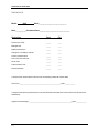
Performance Verification
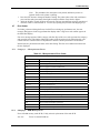
TEST RESULTS
Model:
N-20
Serial:_____________________________
Date:___________Customer Name:________________________________
Description
Pass
Fail
Performance Tests
_____
____
Backlight Test
_____
____
Battery Performance
_____
____
Testing the Low Battery Indicator
_____
____
Power-Up Performance
_____
____
How to Run the Self-Test
_____
____
Printer Test
_____
____
Pulse Oximeter Test
_____
____
Normal Operation
_____
____
I certify that the monitor listed in this form has successfully passed all of these tests.
Technician:_________________________________________________Date:____________
I certify that the above signed technician has performed the tests listed on this form and the monitor performs
satisfactorily.
Support Center Manager:___________________________________________________Date:____________
3-6
4
TROUBLESHOOTING
4.1 How to Use This Section
4.2 Who Should Perform Repairs
4.3 Replacement Level Supported
4.4 Obtaining Replacement Parts
4.5 Troubleshooting Guide
4.6 Service Procedures
4.7 Error Codes
WARNING: Disassembly of the instrument exposes hazardous voltages. To avoid
injury or instrument damage, disassembly or maintenance must be attempted only by
qualified service personnel.
4.1
How to Use this Section
This section explains how to identify and correct monitor difficulties and provides procedures for
common service-related activities, such as battery replacement, clearing paper jams, and adjusting
printer darkness.
Use this section in conjunction with Section 3, Performance Verification, and Section 6, Spare Parts.
To remove and replace a part you suspect is defective, follow the instructions in Section 5,
Disassembly Guide. The functional circuit analysis, located in the Technical Supplement at the end of
this manual, offers information on how the device functions, as well as part locator diagrams and
detailed schematic diagrams.
4.2
Who Should Perform Repairs
Only qualified service personnel should open the device housing, remove and replace components, or
make adjustments. If your medical facility does not have qualified service personnel, contact Nellcor
Technical Services.
4.3
Replacement Level Supported
The replacement level supported for this product is to the printed circuit board (PCB) and major
subassembly level. Once you isolate a suspected PCB, replace the PCB with a known good PCB.
Check to see that the trouble symptom disappears and the device passes all performance tests. If the
trouble symptom persists, swap the replacement PCB and the suspected malfunctioning PCB (the
original PCB that was installed when you started troubleshooting) and continue troubleshooting as
directed.
4.4
Obtaining Replacement Parts
Nellcor Technical Services provides technical assistance information and replacement parts. To obtain
replacement parts, contact Nellcor. Refer to parts by the part names and part numbers listed in Section
6, Spare Parts.
4-1
Troubleshooting
4.5
Troubleshooting Guide
This section discusses potential symptoms, possible causes, and actions for their resolution. Should
this troubleshooting guide fail to address the symptoms evident in a particular N-20/N-20P, please
contact Nellcor's Technical Services Department or a local Nellcor representative for assistance.
If the N-20/N-20P does not perform as expected:
•
•
Check for proper sensor placement.
Depending on concentration, indocyanine green, methylene blue, and other intravascular dyes
may affect the accuracy of a measurement.
• These instruments are calibrated to read oxygen saturation of functional arterial hemoglobin
(saturation of hemoglobin functionally capable of transporting oxygen in the arteries), and
significant levels of dysfunctional hemoglobins such as carboxyhemoglobin or methemoglobin
may affect the accuracy of a measurement.
If the electronics and/or display functions require testing, refer to Section 3, Performance
Verification.
Symptom 1: No response to Measure button.
Cause
4-2
Action
Battery access door may not be properly latched.
Check access door and ensure it is properly
latched.
Batteries may be discharged.
Exchange them for a new set.
Batteries may be incorrectly installed.
Ensure that batteries are oriented according
to the polarity indicator.
Batteries may not be making proper electrical contact.
Inspect contacts for deformity; clean contacts
to remove oxidization.
Fuse F1 on the auxiliary PCB may be open.
See paragraph 4.6.5, Fuse Replacement.
Dust may have accumulated under Measure button causing
loss of electrical contact.
Clean contact points under Measure button
(see Section 5.3, N-20 Disassembly Guide).
Troubleshooting
Symptom 2: Pulse Search indicator appears for more than 5-10
seconds.
Cause
Action
Sensor may be improperly positioned.
Ensure the sensor is correctly applied (see
sensor directions for use).
Incorrect sensor may be in use.
See sensor directions for use to ensure that
the patient's weight and sensor application is
correct. Test the sensor on another person to
verify proper operation.
Perfusion may be too low.
Check patient status. Test the instrument on
someone else, or try another type of sensor.
The N-20/N-20P will not make a
measurement if perfusion is inadequate.
Foreign material on the sensor LEDs or photodetector may be
affecting performance.
Clean the test area and ensure that nothing
blocks the sensor site.
Patient motion may be interfering with the instrument's ability
to find a pulse pattern.
If possible, ask the patient to remain still.
Verify that the sensor is securely applied and
replace it if necessary, move it to a new site,
or use a sensor that tolerates patient
movement, such as an appropriate adhesive
sensor.
Environmental motion may be interfering with the
instrument's ability to track a pulse
The sensor may be too tight, there may be excessive
illumination (e.g., a surgical or bilirubin lamp or direct
sunlight), or the sensor may be placed on an extremity with a
blood pressure cuff, arterial catheter, or intravascular line.
The DB-9 sensor connector on the N-20/N-20P may be
broken.
Symptom 3:
Replace the DB-9 connector (Section 4.6.6).
Pulse Search indicator appears after successful
measurements have been made.
Cause
Action
Patient perfusion may be too low.
Check patient status. Test the instrument on
someone else, or try another type of sensor.
The N-20/N-20P will not make a
measurement if perfusion is inadequate.
Patient motion may be interfering with the instrument's ability
to find a pulse pattern.
If possible, ask the patient to remain still.
Verify that the sensor is securely applied and
replace it if necessary, move it to a new site,
or use a sensor that tolerates patient
movement, such as an appropriate adhesive
sensor.
Environmental motion may be interfering with the
instrument's ability to track a pulse.
The sensor may be too tight, there may be excessive
illumination (e.g., a surgical or bilirubin lamp or direct
sunlight), or the sensor may be placed on an extremity with a
blood pressure cuff, arterial catheter, or intravascular line.
Symptom 4:
Dashes (– – –) appear in the display.
Cause
The sensor is not connected to the instrument.
Symptom 5:
Action
Check all sensor connections; try substituting
another sensor. Check all extension cables. If
an extension cable is in use, remove it and
plug the sensor directly into the instrument.
Pr Err is displayed during the Power-On Self-Test (N-20P only).
4-3
Troubleshooting
Cause
The printer is not operational, but the N-20P continues to
obtain patient measurements.
Symptom 6:
Action
Check to see if the paper is jammed.
Examine the print head and ensure that it has
returned to the home position.
Err followed by a number appears on the display.
Cause
See Section 4.7 for error codes.
Symptom 7:
Action
Record the number that is displayed.
Time or date is incorrect (N-20P only).
Cause
The real-time clock (RTC) battery may be exhausted.
Action
Replace the RTC battery (see Section 4.6.4).
Reset the time and date (see Section 4.6.3).
Symptom 8:
Printer fails to operate (N-20P only).
Cause
Fuse F2 on the auxiliary PCB may be open.
Symptom 9:
only).
Action
See paragraph 4.6.5 for information about
fuses.
Printer paper advances but instrument does not print (N-20P
Cause
The thermal paper may be improperly loaded; characters can
be printed on only one side of the thermal paper roll.
Action
Ensure that the thermal paper is properly
loaded; if needed, remove the roll of printer
paper and reload the printer paper.
Symptom 10: Paper mechanism jams (N-20P only).
Cause
Action
Note: If a printer paper jam is detected during Power-On Self-Test, Pr Err may appear on the display.
Switch off the N-20P. Then check to see if
the print head is at the home position; if so,
attempt to pull the paper out by pulling
gently—do not force it.
If the print head is not at the home position,
and the paper cannot be easily pulled out
from the printer, then the printer may need to
be disassembled to remove the paper jam
(see Sections 5.3, N-20 Disassembly
Procedure, and 4.6.2, Loading/Clearing
Printer Paper).
4.6
Service Procedures
The following service procedures are most likely to be encountered by the service technician. The
PCB designation for a component appears in parentheses, for example, (BT1) or (U15).
4-4
Troubleshooting
4.6.1
Installing Batteries
1. Remove the battery cover access door by pressing the battery compartment access door latch.
2. Install four alkaline "C" cell batteries. Be sure to observe the polarity indicator
sticker.
3. Replace the battery cover access door.
4.6.2
Loading/Clearing Printer Paper
The N-20P uses a thermal paper that can show printed characters on one side only. Make sure that the
paper roll is correctly installed; always refer to the graphical instruction label found on the paper roll.
1. Press down and outward on the top of the paper compartment door to remove it.
2. Feed the paper into the paper compartment slot; refer to the graphic label for orientation.
3. Press and hold the ADV button until the end of the paper appears at the paper exit slot.
4. Replace the paper compartment door.
If the paper jams either during the loading process or during printing, proceed as follows:
1.
Remove both the paper door and the printer-head access cover.
2.
Firmly grab and pull the paper roll backward—out and away from the print head—observe
the access to the print head to determine whether or not the paper escaped from the jammed
position.
3.
If paper remains jammed between the print head and printer, press the ADV button; the
jammed paper may work its way out. If the paper remains jammed, and the printer drive does
not advance the paper, manually advance the drive gear on the side of the printer to free the
paper.
4.
If these attempts fail to free the jammed paper, remove the printer from the unit to gain full
access (see paragraph 5.3, N-20 Disassembly Procedure).
4.6.3
Setting Date and Time
The following procedure applies to the N-20P only.
The following code letters and numbers appear in both Oxygen Saturation and Pulse Rate display
fields. The symbol "xx" represents information in the Oxygen Saturation display field and "yy"
represents information in the Pulse Rate display field.
Begin this procedure by first removing any sensor from the instrument.
1.
2.
3.
4.
5.
6.
7.
8.
9.
10.
11.
12.
Turn on the monitor without the sensor connected. Switch on the N-20P and allow the
unit to run the Power-On Self-Test.
When dashes appear in the Oxygen Saturation and Pulse Rate displays, press the D/D
(day/date) button once. At this point, the Oxygen Saturation display field shows "txx", with
"t" representing time; "xx" representing hours, and "yy" representing minutes. Note that "xx"
(hours) is flashing.
Press the ADV (advance) button repeatedly until the correct hour is displayed.
Press the D/D button once. Note that "yy" (minutes) is now flashing.
Press the ADV button repeatedly until the correct minute is displayed.
At this point, the Oxygen Saturation display field shows "dxx", with "d" representing date;
"xx" representing the month, and "yy" representing the date. Note that "xx" (month) is
flashing.
Press the ADV button repeatedly until the correct month is displayed.
Press the D/D button once. Note that "yy" (date) is flashing.
Press the ADV button repeatedly until the correct date is displayed.
Press the D/D button. At this point, the Oxygen Saturation display field shows "Yxx", with
"Y" representing "year.” Note that "xx" (year number) is flashing.
Press the ADV button repeatedly until the correct year number is displayed.
Press the D/D button once. The N-20P turns itself off within 5 seconds.
4-5
Troubleshooting
13.
4.6.4
Date and time are now correct. Check by switching on the N-20P with the printer enabled.
After the N-20P executes its Power-On Self-Test, the printer prints the spot check mode
header with the correct date and time.
Replacing the Real-Time Clock (RTC) Battery
The socket for the RTC battery (BT1) is located on the auxiliary PCB at grid location 5D. Typical
life of the clock battery is 5 years.
1.
Disassemble the N-20 (see Section 5.3, N-20, Disassembly Procedure).
2.
Using a thin flathead screwdriver, gently pry the RTC battery from its socket.
3.
Insert a new battery into the socket, observing the polarity indication (socket's clip and
battery's flat side are positive).
4.
Reassemble the unit.
5.
Reset the clock (see paragraph 4.6.3, Setting Date and Time).
4.6.5
Replacing Fuses
Two fuses (F1 and F2) are located on the auxiliary PCB. Fuse F1 may open to protect the CPU and its
associated components from damage if the power supply malfunctions. Fuse F2 may open to protect
the printer from damage due to excessive voltage if the printer head jams or has been physically
damaged. Refer to the auxiliary PCB schematic for the locations of F1 and F2.
4.6.6
Replacing the DB-9 Connector
1. Disassemble the N-20 (see Section 5.2); the connector is on the main PCB at grid location 3A.
2. Using a low-power soldering iron, unsolder the connector from the PCB and remove it. Save all
Teflon tubing, ferrite blocks, and insulating materials for the replacement connector.
3. Install ferrite blocks between plastic lead spacer on the connector and the PCB.
4. Insulate connector pin numbers 2, 3, and 5 with Teflon tubing, and insert inside ferrite block.
5. Add insulating material between each end of ferrite block and PCB, and secure with Loctite glue.
6. Solder new connector to PCB and visually check PCB for stray drops of solder before
reassembling.
7. Switch on the N-20/N-20P and test the connector with a patient sensor.
4.6.7
Adjusting Printer Darkness
Caution: Adjust the printer darkness setting until the lightest legible print is visible.
Setting the print darker than this could reduce the life of the printer-head. Although the N-20P is
designed to automatically compensate for conditions that might influence the quality of the printout,
the user may want to adjust the print darkness. The normal darkness setting is set at the factory; this
setting maximizes both readability and life of the printer-head.
1. Switch on the N-20P in spot check mode. (Depressing the instrument Measure button once starts
Spot-check mode.)
2. Simultaneously press and hold the ADV and ON buttons for 2 seconds. If these buttons are not
pressed at the same time, two audible beeps will sound and the N-20P either advances the paper
or switches off, depending on which button press is first sensed. If the buttons are pressed at the
same time, a single audible beep will sound, Pr SEt is displayed, and the printer prints one of the
following 6 lines:
PRINTING LIGHTER
PRINTING LIGHT
PRINTING NORMAL
PRINTING DARK
PRINTING DARKER
PRINTING DARKEST
4-6
(10% lighter than normal darkness)
(5% lighter than normal)
(normal darkness)
(5% darker than normal)
(10% darker than normal)
(15% darker than normal)
Troubleshooting
Note: The parenthetic line description is not printed, and button presses are
ignored whenever the printer is printing.
1. Press the ADV button to change the darkness setting. The printer prints a line with each button
press, and the setting increments from lighter to darkest and then wraps back to lighter.
2. Allow the N-20P to switch off (about 30 seconds). The last print darkness setting is remembered
when the N-20P is switched back on. Test this by repeating the procedure and skipping step 3.
4.7
Error Codes
If a failure is detected during the Power-On Self-Test or during any performance test, the error
message (Err) appears in the Oxygen Saturation display and a 3-digit error code number appears in
the Pulse Rate display.
If an error message appears, find its category (the first digit of the error code represents the category)
and record the error code number. Match the number to the description in the following table, and
contact Nellcor's Technical Services Department or Nellcor's local representative for assistance.
Internal tests are performed in the order of the table listing. The first error condition encountered is
the one displayed.
4.7.1
Category 1 — Microprocessor Errors
Table 4-1: Microprocessor Error Codes
Errors in the CPU (main PCB). Likely action is replacement of the CPU.
4.7.2
101
Error in internal RAM registers test
102
Error in zero register test
103
Error in register contents clearing test
104
Error in register contents increment test
105
Error in register contents decrement test
106–109
Errors in logical operations test
110
Error in exchange test
111
Error in timer tests
112
Error in window select register test
113, 114
Errors in stack manipulation test
115–117
Errors in CPU flags test
118
Error in interrupt pending register test
119
Error in program counter test
120
Error in CPU serial port test
121
Error in pulse width modulation register test
122
Error in A/D register test
123
Error in addressing modes test
124
Error in high speed input register test
125
Error in content addressable memory test
126–129
Errors in arithmetic operations test
Category 2 — RAM Memory Errors
Errors in RAM memory (main PCB). Likely action is replacement of the main PCB.
201–203
Errors in external RAM test
4-7
Troubleshooting
4.7.3
Category 3 — PROM Errors
Errors in PROM memory (main PCB). Likely action is replacement of the PROM.
301
4.7.4
Error in PROM test
Category 4 — I/O Port Errors
Errors in the CPU's internal I/O port (main PCB). Likely action is replacement of either the CPU or
the main PCB.
401–409
Errors in I/O port test
4.7.5
Category 5 — Reserved
4.7.6
Category 6 — Clock Errors
Failure of the real-time clock (auxiliary PCB), or timing differences between the CPU’s clock and the
real-time clock. Likely action is replacement of the main or auxiliary PCB.
4.7.7
601
Failure of real-time clock
602, 603
Errors in real-time clock
Category 7 — Watchdog-Timer Errors
Error in the watchdog-timer circuit of the CPU (main PCB). Likely action is replacement of the CPU.
701, 702
4.7.8
Errors in watchdog-timer
Category 8 — Printer Errors
Error in the printer (see Section 5.1, Troubleshooting).
If a printer error condition occurs, no error code number will display, rather the display reads Pr Err.
4-8
5
DISASSEMBLY GUIDE
5.1 Introduction
5.2 Required Equipment/Tools
5.3 N-20 Disassembly Procedure
5.4 N-20P Disassembly Procedure
WARNING: Only qualified service personnel must perform repair and testing. Improper
repair and/or adjustment may compromise patient safety or the accuracy of the instrument.
5.1
Introduction
The N-20/N-20P can be disassembled down to all major component parts, including:
•
•
•
•
PCBs
battery
cables
chassis enclosures
WARNING: Before attempting to open or disassemble the N-20/N-20P, disconnect the
power cord.
Caution: Observe ESD (electrostatic discharge) precautions when working within the unit.
Note: Some spare parts have a business reply card attached. When you receive these
spare parts, please fill out and return the card.
5.2
Required Equipment/Tools
•
•
•
•
•
•
•
5.2.1
Screwdriver, Phillips-head, small
Screwdriver, Phillips-head, medium
Pliers, long nose
Screwdriver, small flathead
Soldering iron, low-power
Screwdriver, small blade
Needle-nose pliers
N-20 Disassembly Procedure
Whenever repair or disassembly is required, always wear a ground strap connected to active ground.
Before any disassembly or service procedure, switch instrument power off.
5-1
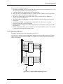
Disassembly Guide
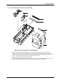
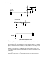
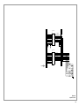
20
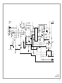
21
34
19
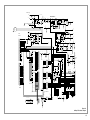
Figure 5-1: Sensor Lock, and Printer, Paper, and Battery Access Doors
1. Remove the battery door (19) and batteries.
2. Remove the sensor lock (34) by lightly pressing in on its ears and pulling out from the sensor
shroud.
3. Remove the paper door (20) and paper roll, and the printer door (21).
5-2
Disassembly Guide
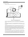
5.2.2
Removing the Covers
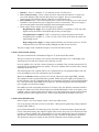
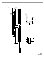
16
18
27
26
15
31
30
Figure 5-2: N-20 Covers with the PCB and Display Assembly
1. Remove screw cap (30), and loosen the captive screw (31), which secures the rear cover (15).
2. Separate the front cover (16) from the rear cover by wedging a thin flathead screw driver between
the covers at the base of the instrument and slowly prying them apart.
Note: The covers are hinged at the top end in a different way; do not attempt to
separate the covers using this technique at the top of the instrument. Once the covers
are separated at the bottom end, lift away the bottom end of the front cover first,
allowing the tabs at the top end to act as a hinge.
5-3
Disassembly Guide
5.2.3
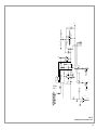
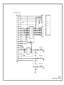
Removing the PCBs and Display Assembly
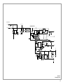
Tab #1
Tab #3
18
Detail B
Flex #1
6
Tab #4
Tab #2
Flex #3
Flex #2
Detail A
5
27
11
12
13
26
Figure 5-3: Main, Auxiliary, and Display PCB Assembly
1. Remove the Measure button (6) from the main PCB.
2. Remove the entire PCB/Taliq display assembly from the rear cover by tilting opposite the
Battery-Check button (5).
3. Raise the locking tabs on the connectors (11, 12, and 13) to release the cable, on the auxiliary
PCB (26), and remove the three flex display circuits.
4. Separate the auxiliary PCB from the main PCB (27) by pulling the PCB headers apart at the base.
5. Remove the display assembly (18) from the main PCB by unsoldering the four tabs that are
physically bent around the main PCB. These tabs are bent to ensure contact with the ground
plane of the main PCB.
6. Using a long-nose plier, remove the display assembly by untwisting the four tabs (see Detail A
and B).
5.2.4
N-20P Disassembly Procedure
1. Remove the paper door (20) and any printer paper by firmly grasping the paper roll, and pulling
the roll outward from the printer.
2. See paragraphs 5.2.1 and 5.2.2, N-20 Disassembly Procedure, for removal of covers, PCBs, and
the display assembly.
5-4
Disassembly Guide
5.2.5
Disassembling the Printer/Flex Circuit Assembly
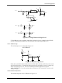
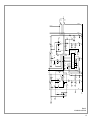
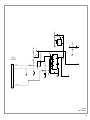
29
32
4
7
37
28
24
Figure 5-4: Printer and Flex Circuit Installation
1. Remove the printer button retaining plate (37) by sliding it away from the case assembly.
2. Disconnect the two flex-circuit headers of the printer (29) from the connectors on the printer flex
circuit (28) by slowly pulling outward from side to side at alternating ends of the connectors.
3. Remove the printer button strip (7) from the printer flex-circuit.
4. Remove the printer flex-circuit insulator (24).
5. Remove printer hold-down bracket (4) from the back cover by removing the Phillips screw (32).
6. Press the printer hold-down bracket into the back cover and remove the printer.
5-5
6
SPARE PARTS
6.1 N-20/N-20P Spare Parts
6.1
N-20/N-20P Spare Parts
To order replacement parts, contact Nellcor's Technical Services Department and order by part
number. Item numbers correspond to the callout numbers in the figures.
Item
Designator
Description
P/N
1
SW1
Battery switch (auxiliary PCB)
630106
2
BT1
Battery holder (auxiliary PCB)
901582
3
BT1
Battery, lithium (auxiliary PCB)
640112
4
Bracket, printer, hold-down
023133
5
Button, battery-check
023301
Button, measure
022948
6
S2
7
9
Button, measure (European version)
026386
Buttons, printer, strip
022947
Buttons, printer, strip (European version)
026387
Connector shield, DB-9
023467
10
P1
Connector, DB-9
463103
11
JP17, JP18
Connector, pin header 10x2, low profile (auxiliary PCB)
491244
12
JP5
Connector, ZIF, flex, 7-pin (auxiliary PCB)
491242
13
JP9
Connector, ZIF, flex, 22-pin (auxiliary PCB)
491250
14
JP2,3
Connector, ZIF, flex, 32-pin (auxiliary PCB)
491243
15
16
17
D8
18
Cover, rear (non-printer model)
022929
Cover, rear (printer model)
026339
Cover, front, with gasket assembly
022921
Diode, photo, 8440 (main PCB)
591017
Display, Taliq, analog shield assembly
024466
Display, Taliq, analog shield assembly (European version)
026765
19
Door, battery
022924
20
Door, paper.
022938
21
Door, printer
026338
22
F2
Fuse, micro, 1 amp (auxiliary PCB)
691236
23
F1
Fuse, micro, 1.5 amp (auxiliary PCB)
691239
Insulator, printer
026139
25
Nut, keps,SS, 4-40
851101
26
PCB, auxiliary
024472
27
PCB, main
024468
28
Printer flex circuit
024464
29
Printer
024462
30
Screw cap
023451
24
6-1
Spare Parts
Item
Description
P/N
31
Screw, captive
891324
32
Screw, Phillips, 4-40 ×1/4
801025
33
Screw, plastite
871031
34
Sensor lock
022943
35
Sensor shroud
022944
36
Spacer
023452
37
Stiffener, printer button
023131
38
Tape, foam (.88" ×.38")
023300
Transducer, audio, piezo ceramic
691230
39
6-2
Designator
BZ1
7
PACKING FOR SHIPMENT
7.1 General Instructions
7.2 Repacking in Original Carton
7.3 Repacking in a Different Carton
Should you need to ship the N-20/N-20P monitor for any reason, follow the instructions in this
section.
7.1
General Instructions
Pack the monitor or printer carefully. Failure to follow the instructions in this section may result in
loss or damage not covered by the Nellcor warranty. If the original shipping carton is not available,
use another suitable carton or call Nellcor Technical Services to obtain a shipping carton.
Prior to shipping the device, contact Nellcor Technical Services for a returned goods authorization
(RGA) number. Mark the shipping carton and any shipping forms with the RGA number.
7.2
Repacking in Original Carton
If available, use the original carton and packing materials. Pack the monitor or printer as follows:
Place the monitor, or printer, and, if necessary, accessory items in original packaging.
Place in shipping carton and seal carton with packing tape.
Label carton with shipping address, return address, and RGA number.
7.3
Repacking in a Different Carton
If the original carton is not available:
1. Place the monitor or printer in plastic bag.
2. Locate a corrugated cardboard shipping carton with at least 200 pounds per square inch (psi)
bursting strength.
3. Fill the bottom of the carton with at least 2 inches of packing material.
4. Place the bagged unit on the layer of packing material and fill the box completely with packing
material.
5. Seal the carton with packing tape.
6. Label carton with shipping address, return address, and RGA number.
7-1
8
SPECIFICATIONS
8.1 Readout
8.2 Controls
8.3 Operating Modes
8.4 Printer Output
8.5 N-20/N-20P Performance
8.6 Sensor Types
8.7 Electrical Specifications
8.8 Environmental Specifications
8.9 Physical Specifications
8.10 Quality Information
8.1
Readout
Display shows SpO2 (saturation of arterial hemoglobin oxygen), pulse rate, and pulse amplitude; also
included are a Pulse Search and Low Battery indicator, and an electroluminescent backlight.
8.2
Controls
8.2.1
N-20
The Measure button switches the instrument on and off, and initiates the measurement cycle.
The Battery-Check button is used to check battery condition and switches beeper on and off.
8.2.2
N-20P
The Measure button switches the instrument on, initiates the measurement cycle, and switches
instrument off.
The Battery-Check button is used to check battery condition and switches beeper on and off.
ON button switches the printer on and off.
D/D sets display date and time.
ADV advances paper and increments time and date.
8.3
Operating Modes
8.3.1
Spot Check Mode
Pressing the instrument Measure button once for less than 2 seconds starts the spot check mode. Spot
check mode computes SpO2 averaged over five valid pulses and displays SpO2 and pulse rate at the
end of the measurement interval. If the printer is activated, the printout shows the displayed SpO2 and
pulse rate.
8.3.2
Extended Mode
Extended mode is started by holding down the instrument Measure button for approximately 3
seconds, plus any time required to complete the power-on self-test. The N-20/N-20P displays updated
SpO2 and pulse rate with every pulse (after five valid pulses have been detected). The N-20/N-20P
remains active until 3 minutes after the sensor is removed, or until the instrument is turned off.
8-1
Specifications
For the N-20, a 2% or greater decrease in SpO2 is indicated by two brief, low-pitched tones.
The N-20P printout shows SpO2 and pulse rate at 30-second intervals. For the N-20P, a 2% or greater
decrease in SpO2 is indicated by two brief, low-pitched tones and an asterisk (*) on the printout. At
the end of the measurement period, a header and statistical summary values (minimum, maximum,
and mean of both pulse rate and oxygen saturation) are printed.
8.4
Printer Output
When activated by the printer ON button, the N-20P output shows date, time, SpO2, and pulse rate (in
spot check mode), with space provided for writing in patient identification. The thermal paper
printout measures roughly 40 mm (1.6 in.) by 100 mm (4.0 in.) in size.
If the N-20P is in spot check mode and the printer is turned on any time during a measurement or after
a measurement is taken and before the N-20P powers down, the printer will catch up and print a
complete record of the measurements recorded up to the current moment.
8.5
N-20/N-20P Performance
8.5.1
Range
8.5.2
8.5.3
Saturation:
0–100%
Pulse Rate:
20–250 beats per minute (bpm) ± 1 standard deviation
SpO2 Accuracy 1
Adults:
70–100%
± 2 digits 2
Neonates:
70–100%
± 3 digits 2
Pulse Rate:
20 –250 bpm
± 3 digits 2
Response
In spot check mode, the measurement cycle (from button press to display of data) is five valid pulses.
In extended mode, the instrument measures for a period of up to 30 minutes and continuously displays
updated SpO2 and pulse rate.
1
Accuracies are expressed as plus or minus “X” digits (saturation percentage points) between saturations of
70-100%. This variation equals plus or minus one standard deviation (1SD), which encompasses 68% of the population.
All accuracy specifications are based on testing the subject monitor on healthy adult volunteers in induced hypoxia studies
across the specified range. Adult accuracy is determined with Oxisensor II D-25 sensor. Neonatal accuracy is determined
with Oxisensor II N-25 sensor.
2
This variation equals one SD.
8-2
Specifications
8.6
Sensor Types
Table 8-1: Sensors
Sensor
Model
Patient Size
Oxisensor II oxygen transducers (sterile, single-use only)
N-25/N-25LF
I-20/I-20LF
D-20
D-25/D-25L
R-15
<3 or >40 kg
3 to 20 kg
10 to 50 kg
>30 kg
>50 kg
Oxiband oxygen transducer (reusable with disposable
nonsterile adhesive)
OXI-A/N
OXI-P/I
<3 or >40 kg
3 to 40 kg
Durasensor oxygen transducer (reusable, nonsterile)
DS-100A
>40 kg
Nellcor reflectance oxygen transducer (reusable, nonsterile)
RS-10
>40 kg
Dura-Y multisite oxygen transducer (reusable, nonsterile)
D-YS
>1 kg
D-YSE
>30 kg
D-YSPD
3 to 40 kg
P
N
I
A
10 to 50 kg
<3 or >40 kg
3 to 20 kg
>30 kg
For use with the Dura-Y sensor:
Ear clip (Reusable, nonsterile)
Pedi-Checkpediatric spot-check clip (reusable,
nonsterile)
OxiCliq oxygen transducers (sterile, single-use only)
8.7
Electrical Specifications
8.7.1
Battery
Type:
four 1.5-V alkaline "C" cell batteries
Battery Capacity:
typically 37 hours for N-20
typically 32 hours for N-20P
8.7.2
Instrument
Power Requirements:
4–6 VDC, supplied by battery only
Leakage Current:
Meets applicable IEC- 601 and AAMI/ANSI standards;
the N-20/N-20P has no power or ground connections
Patient Isolation:No electrical connection to patient (inherently insulated)
8.8
Environmental Specifications
8.8.1
Operating Temperature
Instrument:
0 to 40 °C (32 to 104 °F)
8-3
Specifications
8.8.2
Storage Temperature
-20 to 50 °C (4 to 122 °F)
8.9
Humidity:
Any humidity/temperature combination without condensation
Altitude:
0 to 6200 meters (0 to 20,000 ft)
Physical Specifications
Physical specifications are based on product without the protective boot.
8.9.1
8.9.2
Weight (with batteries installed)
N-20:
0.6 kg (1.3 lb)
N-20P:
0.62 kg (1.4 lb)
Dimensions
N-20:
19.0 cm high ×7.6 cm wide ×5.08 cm deep
(7.5 in. ×3.0 in. ×2.0 in.)
N-20P:
19.0 cm high ×7.6 cm wide ×6.35 cm deep
(7.5 in. ×3.0 in. ×2.5 in.)
8.10 Qualifying Information
The Nellcor N-20/N-20P is calibrated to measure arterial hemoglobin oxygen saturation of functional
hemoglobin. The specified accuracy of this measurement is based on statistical analysis of arterial
blood samples as measured on an IL282 CO-Oximeter.
Indocyanine green, methylene blue, and other intravascular dyes, depending on concentration, may
interfere with the accuracy of data obtained from the instrument. Carboxyhemoglobin or other
dyshemoglobins may also interfere with the accuracy of the data if present in significant
concentration.
8-4
9
TECHNICAL SUPPLEMENT
9.1 Overview
9.2 Functional versus Fractional Saturation
9.3 Measured versus Calculated Saturation
9.4 Circuit Analysis
9.5 Functional Overview
9.6 Definition of Terms
9.7 Overall Block Diagram
9.8 SpO2 Analog Circuit
9.9 Digital Circuitry
9.10 Circuit Illustrations
9.1
Overview
The N-20/N-20P is based on the principles of spectrophotometry and optical plethysmography.
Optical plethysmography uses light absorption technology to reproduce wave forms produced by
pulsatile blood. The changes that occur in the absorption of light due to vascular bed changes are
reproduced by the pulse oximeter as plethysmographic wave form.
Spectrophotometry uses various wavelengths of light to qualitatively measure light absorption
through given substances. Many times each second, the N-20/N-20P passes red and infrared light into
the sensor site and determines absorption. The measurements, which are taken during the arterial
pulse, reflect absorption by arterial blood, nonpulsatile blood, and tissue. The measurements that are
obtained between arterial pulses reflect absorption by nonpulsatile blood and tissue.
By correcting "during pulse" absorption for "between pulse" absorption, the N-20/N-20P determines
red and infrared absorption by pulsatile arterial blood. Because oxyhemoglobin and
deoxyhemoglobin differ in red and infrared absorption, this corrected measurement can be used to
determine the percent of oxyhemoglobin in arterial blood: SpO2 is the ratio of corrected absorption at
each wavelength.
9.2
Functional versus Fractional Saturation
The N-20/N-20P measures functional saturation, that is, oxygenated hemoglobin expressed as a
percentage of the hemoglobin that is capable of transporting oxygen. It does not detect significant
levels of dyshemoglobins. In contrast, some instruments such as the IL282 Co-oximeter measure
fractional saturation, that is, oxygenated hemoglobin expressed as a percentage of all measured
hemoglobin, including dyshemoglobins.
Consequently, before comparing N-20/N-20P measurements with those obtained by an instrument that
measures fractional saturation, measurements must be converted as follows:
functional saturation =
9.3
fractional saturation
x100
100 - (% carboxyhemoglobin + % methemoglobin)
Measured versus Calculated Saturation
When saturation is calculated from a blood gas measurement of the partial pressure of arterial oxygen
(PaO2), the calculated value may differ from the N-20/N-20P SpO2 measurement. This is because the
calculated saturation may not have been corrected for the effects of variables that can shift the
relationship between PaO2 and saturation.
9-1
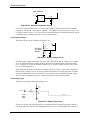
Technical Supplement
Figure 9-1 illustrates the effect that variations in pH, temperature, partial pressure of carbon dioxide
(PCO2), and concentrations of 2,3-DPG and fetal hemoglobin may have on the oxyhemoglobin
dissociation curve.
Saturation (%)
100
50
0
pH
Temperature
PCO2
2,3-DPG
Fetal Hb
pH
Temperature
PCO2
2,3-DPG
50
PO2 (mmHg)
100
Figure 9-1: Oxyhemoglobin Dissociation Curve
9.4
Circuit Analysis
The following paragraphs discuss the circuits of the N-20/N-20P.
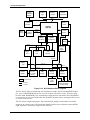
9.5
Functional Overview
This section provides a detailed explanation of N-20/N-20P operation using block diagrams and
circuit schematics.
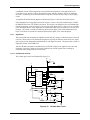
The relationship between these components and their interconnection is illustrated in the overall block
diagram (Figure 9-2). The main component circuitry has been divided into the following subsections:
9-2
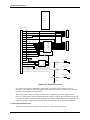
Technical Supplement
Main PCB
Patient
sensor
SpO2 analog
Microprocessor
Memory
Display control
Sensors: temperature
ambient light
battery voltage
Measure
button
PROM
20-pin headers
Auxiliary PCB
Power supply
Printer interface
Display control
Audio beeper
Batteries
4-6 VDC
Flex
connectors
Check
battery
button
Realtime
clock
Display
backlight
Printer
flex circuit
Printer
N-20P only
Figure 9-2: Overall Block Diagram
9.6
SpO2 Analog Circuitry Block Diagram (Figure 9-3)
Analog circuitry has high signal sensitivity and reduced susceptibility to noise. Its design allows for a
wide range of input signal levels and a broad range of pulsatile modulation. The SpO2 analog circuit
(Figure 9-3) consists of four subsections:
1. Sensor output/LED control, where the CPU controls the gain of both LEDs so that signals
received at the input amplifier are in its acceptable dynamic range
2. Input signal conditioning, where sensor output current is converted to voltage
3. Signal gain, where the separated LED signals are amplified so their current levels are within the
A/D converter's acceptable range; and
4. AC ranging, where DC offset is eliminated from each LED signal.
Patient
sensor
LEDs
Input signal
conditioning
photocurrent
to voltage
conversion
demutiplexed
to 2 channels
Main PCB
Signal gain
AC Ranging
variable gain,
filtered for
each LED
channel
offset
substraction;
additional gain
and filtering
Main PCB
Main PCB
Microprocessor
Main PCB
LED drivers
(red & IR)
Main PCB
Control
To digital section
Figure 9-3: SpO2 Analog Circuitry Block Diagram
9-3
Technical Supplement
9.6.1
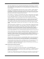
Digital Circuitry Block Diagram (Figure 9-4)
Figure 9-4 shows the N-20/N-20P hardware and circuits, which include the CPU and system memory,
the power supply and power control circuitry, user controls, display and ambient light sensors, audio
output, thermal printer (N-20P only) and ambient temperature sensor, and the real-time clock.
Measure
Check Battery
Power supply
& control
N-20/N-20P Control buttons
AUX
PCB
Ambient
light sensor
Main
PCB
AUX PCB
CPU
Display
drivers
Main PCB
Display
Audio beeper
Memory
&
software
AUX PCB
(N-20 only)
Printer
To analog section
Real-time
clock
AUX
PCB
Ambient
temp. sensor
Main
PCB
ON
ADV
Printer Control button
D/D
Figure 9-4: Digital Circuitry Block Diagram
9.6.2
Power Supply Block Diagram (Figure 9-5)
Power supply circuitry (Figure 9-5) is located on the auxiliary PCB and consists of four subsections:
1. Four "C" size batteries that provide 4-6 VDC
2. Power control circuitry that senses a press of the Measure button and switches power on
3. Power shutoff circuit that controls power to all circuits except the power control circuit
4. Power supply circuits include a regulated power supply at 5 VDC, unregulated power supplies of
-5 VDC, 10 VDC, and 12 VDC, and a high voltage power supply of 70 VDC.
Measure
button
AUX PCB
Disposable
batteries
4-6 VDC
Power
control
circuits
AUX PCB
Main PCB
+5 VDC
Power
shutoff
circuits
(fuse,
EMI protect,
ESD protect)
Power
supply
circuits
+70 VDC
Microprocessor
Display drivers
AUX PCB
Display backlight
-5
VDC
+10
VDC
+12
VDC
SpO2
Analog
section
(main board)
Figure 9-5: Power Supply Block Diagram
9-4
Technical Supplement
9.6.3
Display Control Block Diagram (Figure 9-6)
The N-20/N-20P display is controlled by the display control circuitry (see Figure 9-6). A sensor is
used to measure ambient light. During low light conditions, the display backlight, an
electroluminescent device, is automatically switched on.
Main PCB
Microprocessor
Main PCB
AUX PCB
Control
conditioning
circuit
(generates
timing
signals)
Display driver
(1)
Display
Display driver
(2)
Display
backlight
AUX PCB
High voltage
control circuit
(enables
+70 VDC
to display)
70 volts
Figure 9-6: Display Control Block Diagram
9.6.4
Printer Control Block Diagram (Figure 9-7)
Printer circuitry (Figure 9-7) is divided into two subsections: the printer interface and the printer flex
circuit. The printer interface circuitry is present on all models, but is disabled by software in the
N-20. The printer flex circuit is added when a printer is present.
Main PCB
Microprocessor
N-20 only
AUX PCB
Printer
interface
Printer
flex
circuit
(N-20P only)
PCB
On
ADV D/D
Printer
(N-20 only)
User push buttons
Figure 9-7: Printer Control Block Diagram
9.7
Definition of Terms
9.7.1
Analog to Digital (A/D) converter
The CPU has a 10-bit A/D converter on board. Up to eight different analog inputs can be provided to
the A/D for measurement.
9.7.2
Central Processing Unit (CPU)
An Intel 80C196KC 16-bit microcontroller. The CPU sends and receives control signals to the SpO2
analog section, display, and optional printer.
9.7.3
Content Addressable Memory (CAM)
The CPU controls the HSO lines with the CAM. CAM is software controlled and programmed with
events scheduled relative to one of two internal timers.
9-5
Technical Supplement
9.7.4
High Speed Outputs (HSO)
The 6 HSO lines control most of the timing of the LED signal pulse and the demodulation of the
received signal.
9.7.5
Input and Output (I/O)
Input and Output (I/O) are digital lines that are used by the CPU to read in data and output data.
9.7.6
Light-Emitting Diodes (LEDs)
Two LEDs are used in Nellcor oximetry sensors. Light is transmitted through body tissue and
received by a photodetector circuit that converts it to photocurrent. The two wavelengths, which are
used for calculation of pulse rate and oxygen saturation in blood, are transmitted at the following
frequencies:
•
•
9.7.7
infrared (IR) light at approximately 915 microns
red light at approximately 660 microns
Pulse Width Modulation (PWM)
The three 8-bit PWM outputs can be software controlled; their duty cycle can be changed from
0-255/256 of the total pulse duration. PWM frequency is the crystal frequency of the CPU, which is
10 MHz divided by 1024. The PWMs control the gains within the analog circuit.
9.7.8
RCal
Sensor RCal value is a resistance value specific to an individual sensor. This value is used by the
software during oxygen saturation computations to maximize accuracy.
9.7.9
Real-Time Clock (RTC)
The RTC is used with the optional printer to track time and date for printouts.
9.8
Overall Block Diagram
Exclusive of covers, buttons, and external connectors, the N-20/N-20P consists of three main
components: the main PCB, the auxiliary PCB, and the display assembly and analog shield.
9.8.1
Main PCB
Contains the SpO2 analog circuitry; the CPU; support memory circuits; sensor circuits for ambient
light, temperature, and battery voltage; the check battery circuit; a serial data port; and some display
control circuits.
9.8.2
Auxiliary PCB
Contains the power supply circuitry; the display driver circuits; the real-time clock; the interface
circuitry for the printer flex circuit board (which is not used unless a printer is present); and audio
output hardware.
9.8.3
Display and Analog Shield Assembly
This assembly connects to the main PCB by flex circuits. A metal shield shrouds the SpO2 analog
circuits on the main PCB to protect them from EMI. An integrated electroluminescent backlight
illuminates the display under low light conditions.
The N-20P has an additional printer control board (printer flex circuit) and printer hardware. The
following block diagram shows the relationship between these components.
9-6
Technical Supplement
9.9
SpO2 Analog Circuitry
This subsection describes the SpO2 analog hardware. The analog circuitry has high signal sensitivity
and reduced susceptibility to noise. Its design allows for a wide range of input signal levels and a
broad range of pulsatile modulation. The SpO2 analog block diagram (Figure 9-3) consists of four
subsections:
9.9.1
Sensor Output/LED Control
The CPU controls the gain of both LEDs so that signals received at the input amplifier are within an
acceptable dynamic range. Signal channel gain may also need to be increased. The CPU uses PWM
lines to control LED current level or to amplify the signal channel.
9.9.2
Input Conditioning
Sensor output current is converted to voltage. A demodulation circuit minimizes the effects of other
light sources and stray frequency inputs. Because the IR and RED signals are at different current
levels, the two LED signals are demultiplexed and separately amplified, so they can be compared with
each other. Two circuits handle the demultiplexing by alternately selecting LED signals using
switches. Filters then remove noise and smooth the signals before sending them to the amplifiers.
9.9.3
Signal Gain
The separated LED signals are amplified so that their current levels are within the A/D converter's
acceptable range. The signals are filtered to improve the signal-to-noise ratio, and clamped to a
reference voltage.
9.9.4
AC Ranging
DC offset is eliminated from each LED signal. An analog switch sets the mean signal value to the
mean of the A/D converter range, and the AC modulation is superimposed on that DC level. Then,
each AC signal is amplified and filtered to eliminate residual effects of the PWM modulations.
Finally, these two signals are input to the CPU A/D converter.
The relationship between these subsections is shown in the following block diagram.
9.9.5
Sensor Output/LED Control
The SpO2 analog circuitry provides control of the red and IR LEDs such that the received signals are
within the dynamic range of the input amplifier. Because excessive current to the LEDs will induce
changes in their spectral output, it is sometimes necessary to increase the received signal channel
gain. To that point, the CPU controls both the current to the LEDs, and the amplification in the signal
channel.
At initialization of transmission, the LEDs' intensity level is based on previous running conditions,
and the transmission intensity is adjusted until the received signals match the range of the A/D
converter. If the LEDs reach maximum output without the necessary signal strength, the PWMs will
increase the channel gain. The PWM lines will select either a change in the LED current or signal
gain, but will not do both simultaneously.
The LED circuit switches between red and IR transmission and disables both for a time between
transmissions in order to provide a no-transmission reference. To prevent excessive heat build-up and
prolong battery life, each LED is on for only a small portion of the duty cycle. Also, the frequency of
switching is well above that of motion artifact and not a harmonic of known AC transmissions. The
LED switching frequency is 1.485 kHz. The IR transmission alone, and the red transmission alone
will each be on for about one-fifth of the duty cycle; this cycle is controlled by the HSOs of the CPU.
9-7
Technical Supplement
9.9.5.1 LED Drive Circuit
The LED drive circuit is illustrated in Figure 9-8 (at the end of this section).
The IR and red LEDs are separately controlled with their drives’ currents multiplexed over two shared
wires. Current to the IR LED is in the range of 4.3-50.0 mA; and, current to the red LED is in the
range of 6.5-75.0 mA. Currents are limited to less than 100 mA for two reasons: (1) slight excess
current can potentially change the emission characteristics of the LEDs, and (2) large excess current
could create excessive heat at the sensor site.
The IR/red LED transmission signal (HSO1 of the CPU) is fed into the select inputs of the triple
single-pole-double-throw (SPDT) analog multiplexing switch U10, causing either the IR or the red
LED transmission to be enabled.
PWM1, which is filtered by the network of R44, C37, R52, and C38, is input to the LED drive
circuit switch U10, and controls the magnitude of the IR LED current supply.
PWM2, which is filtered by the network of R43, C36, R53, and C39, is also input to U10, and
controls the red LED current magnitude.
Two NPN transistors (Q1 and Q2) act as current sources for the IR and red LED outputs. Two PNP
transistors (Q3 and Q4) act as switches between the IR and red LED output lines. Transistor Q5 acts
as an LED drive current limiter; it clamps output of the current regulator circuit to the required level.
If any resistor in the LED drive circuit fails, current to the LED will still be limited to a safe level.
The RSENS line senses the RCal value and enables the CPU to make the proper calculations based on
the type of sensor being used.
9.9.6
Input Conditioning
Input to the SpO2 analog circuit is the current output of the sensor photodiode. In order to condition
the signal current, it is necessary to convert the current to voltage.
A differential synchronous demodulation circuit is used to reduce the effects of other light sources
and stray frequency inputs to the system. Because the IR and red signals are absorbed differently by
body tissue, their received signal intensities are at different levels. Therefore, the IR and red signals
must be demodulated and then amplified separately in order to compare them to each other.
Demultiplexing is accomplished by means of two circuits that alternately select the IR and red signal.
Two switches that are coordinated with the IR and red transmissions control selection of the circuits.
A filter with a large time constant follows to smooth the signal and remove noise before amplification.
9.9.6.1 Differential Synchronous Demodulation Circuit
The differential synchronous demodulation circuit is illustrated in Figure 9-9 (at the end of this
section).
Before the current from the photodetector is converted to voltage, any high frequency noise is filtered
by C40 and R17. The op-amp U1A is used in parallel with the current-to-voltage converter U1D to
cancel any DC voltage, effectively AC coupling the output of U1D. The average value of the SpO2
analog reference voltage (VREF) of U1D, 5 V, is measured at pin 14 of test point 49.
The same line that controls the on/off pulsing of the LEDs controls U6D, a single-pole-single-throw
(SPST) analog switch. When either of the LEDs are on (the line is low and the switch is closed), U35
is used as a non-inverting amplifier. When the LEDs are both off, U35 is used as an inverting
amplifier. The signal at the output of amplifier U35 is then demultiplexed.
The CPU HSO lines SAMPRED and SAMPIR, which are both active low, control SPST analog
switches U6A and U6B, respectively. Switch U6A is closed to sample the red signal; switch U6B is
closed to sample the IR signal. The sampling rate for both switches is 10 kHz. Switching is
9-8
Technical Supplement
coordinated with the LED transmission so that the IR and red signals are each sampled twice per
cycle; that is, once when the LED is off (signal inverted), and once when the LED is on (signal not
inverted). The filtering circuit that follows has a long time constant, thereby acting as an averaging
circuit.
A simplified N-20 HSO timing diagram is illustrated in Figure 9-10 (at the end of this section).
If the instantaneous average photocurrent (DC offset) is excessive and U1D cannot bring it to VREF,
the PHOTOI line to the CPU (HSI0) is activated. This action is an indication of excess ambient light
into the photosensor, or the occurrence of excess noise in the input circuit. It also serves as a warning
to the instrument that the sensor signal may be contaminated and causes the software to send an error
message. After about 3 seconds of continuous photocurrent signal, pulse search annunciation will
begin. After about 10 seconds of continuous photocurrent signal, zeros will be displayed.
9.9.7
Signal Gain
The separated IR and red signals are amplified so that their DC values are within the range of the A/D
converter. Because the received IR and red signals are typically at different current levels, the signal
gain circuits provide independent amplification for each signal as needed. The gain in these circuits is
adjusted by means of the PWM lines.
After the IR and red signals are amplified, they are filtered to improve the signal-to-noise ratio and
clamped to a reference voltage to prevent the combined AC and DC signal from exceeding an
acceptable input voltage from the A/D converter.
9.9.7.1 Variable Gain Circuits
The variable gain circuits are illustrated in Figure 9-11.
VREF
C122
.1UF
-5V
To LED control
PWM2
OFF/ON
U2
VCC
16
C35
.1UF
7
8
VDD
C
B
A
INH
VEE
VSS
Z1
Z0
4
15
14
Z
Y1
Y0
Y
X1
X0
X
4053
RED
PWM1
IR LED/AV
9
10
11
6
R39
47.5K
3
5
RED
1
2
Q6
C33
13
12
1NF
VREF
2N3906
9
10
LF444
TP51
3.32K
C24
.47UF
Q7
C34
R24
82.5K
C127
220PF
IR
VREF
VREF
IR
U1C
8
R25
82.5K
R26
C126
220PF
1NF
2N3906
6
U1B
7
5
LF444
TP52
Figure 9-11: Variable Gain Circuit
9-9
Technical Supplement
The two variable gain circuits are functionally equivalent. The gain of each circuit is contingent upon
the signals received level and is controlled to bring each signal to approximately 3.5 V. Each circuit
uses an amplifier and one switch in the triple SPDT analog multiplexing unit U2.
The gain in each of the circuits is accomplished by means of a feedback loop, which includes one of
the SPDT switches in U2. The PWMs control whether the feedback loop is connected to ground or to
the amplifier output. The feedback is then averaged by C33/R25 (red), and C34/R24 (IR). The higher
the value of PWM2, the greater the IR gain; the higher the value of PWM1, the greater the red gain.
9.9.7.2 Filtering Circuits
The filtering circuits are illustrated in Figure 9-12.
These circuits consist of two cascaded second-order filters with a break frequency of 10 Hz. Pairs of
diodes (D1/D3 and D2/D4), that are located between VREF and ground at the positive inputs of the
second amplifiers, maintain the voltage output within the range of the A/D converter.
C13
REDDC
TP81
.12UF
RED
R6
C16
100K
U4D
15
R7
U4C
11
.12UF
16
14
OP490SO
100K
R9
R8
100K
C14
10
12
OP490SO
100K
TP89
VREF
CR1
C15
.068UF
1N914
.068UF
TP82
CR3
1N914
+12V
IR
R11
C18
R13
100K
4
.12UF
U4A
2
R10
1
3
OP490SO
100K
C17
.068UF
100K
R12
C19
.12UF
100K
1
3
-5V
U4B
6
7
IRDC
5
OP490SO
VREF
CR2
1N914
TP90
.068UF
C20
CR4
1N914
Figure 9-12: Filtering Circuit
9.9.8
AC Ranging
In order to measure a specified level of oxygen saturation and to still use a standard-type combined
CPU and A/D converter, the DC offset is subtracted from each signal. Because the DC portion of the
signal can be on the order of one thousand times the AC modulation, 16 bits of A/D conversion would
9-10
Technical Supplement
otherwise be required to accurately compare the IR and red modulations between the combined AC
and DC signals. The DC offsets are subtracted by using an analog switch to set the mean signal value
to the mean of the range of the A/D converter whenever necessary. The AC modulation is then
superimposed upon that DC level. This is also known as AC ranging.
Each AC signal is subsequently amplified such that its peak-to-peak values span one-fifth of the range
of the A/D converter. The amplified AC signals are then filtered to remove the residual effects of the
PWM modulations and, finally, are input to the CPU. The combined AC and DC signals for both IR
and red signals are separately input to the A/D converter.
9.9.8.1 Offset Subtraction Circuits
The AC variable gain control circuit is illustrated in Figure 9-13 (at the end of this section). Voltage
dividers R22 and R41 (red), and R31 and R5 (IR), which are located between VREF and ground,
establish a baseline voltage of 2.75 V at the input of the unity gain amplifiers U7C (red) and U7D
(IR).
Whenever SPST analog switches U11A and U11D are closed by HSO0 (active low), the DC portions
of the IR and red signals create a charge, which is stored on C29 and C89, respectively. These
capacitors hold this charge even after the switches are opened and the resulting voltage is subtracted
from the combined signal— leaving only the AC modulation output. This AC signal is superimposed
on the baseline voltage output by U7C and U7D. The IRDC and REDDC are then filtered and input
to the CPU, and can be measured at TP58 and TP54, respectively.
9.9.8.2 AC Variable Gain Control Circuits
The AC variable gain control circuit is illustrated in Figure 9-13 (at the end of this section).
The AC modulations are amplified by U7A (red) and U7B (IR) and superimposed on the baseline
voltages present at the output of U7D (IR) and U7C (red). The amplification is handled by means of
the SPDT analog multiplexing switch U3 within the feedback loop, which increases gain as PWM0 is
increased. The IRAC and REDAC are then filtered and input to the CPU, and can be measured at
TP55 and TP59, respectively.
9.10
Digital Circuitry
The digital hardware and related circuitry, which is illustrated in the following block diagram (Figure
9-4), includes the following subsystems:
9-11
Technical Supplement
Measure
Check Battery
Power supply
& control
N-20/N-20P Control buttons
AUX
PCB
Ambient
light sensor
Main
PCB
AUX PCB
CPU
Display
drivers
Main PCB
Memory
&
software
Display
Audio beeper
AUX PCB
(N-20 only)
Printer
To analog section
Real-time
clock
AUX
PCB
Ambient
temp. sensor
Main
PCB
ON
ADV
D/D
Printer Control button
Figure 9-4: Digital Circuitry Block Diagram
9.10.1
CPU
A 16-bit microcontroller that includes a serial port, watchdog timer, A/D converter with an 8-input
analog multiplexer, 3-pulse width modulators, and a high-speed I/O subsystem.
9.10.2
System Memory
External to the CPU and consists of an 8K ×8 static RAM and a 64K ×16 EPROM.
9.10.3
Real-Time Clock (RTC)
The RTC keeps track of date and time, which is printed on each printout. The RTC is powered by a
lithium battery designed to last up to 5 years before needing replacement.
9.10.4
Audio Output
A piezoelectric ceramic beeper is used for audio output.
9.10.5
Display Control
A high-visibility display provides oxygen saturation and pulse rate values. An ambient light sensor
responds to low-light conditions and turns on the display backlight.
9.10.6
User Controls
A Measure button and a Battery-Check button. The Measure button signals the power control
circuit to switch on the power supply. Press and hold the Battery-Check button to display a
percentage of useful life remaining in the batteries.
9.10.7
Power Supply/Power Control Circuitry
The N-20/N-20P receives power from 4 "C" cell batteries. The power control circuitry discontinues
power to the unit when the batteries are no longer reliable.
9-12
Technical Supplement
9.10.8
Thermal Printer (N-20P only)
Generates a hard copy of oxygen saturation and pulse rate values. A sensor monitors ambient
temperature and adjusts printer output to ensure consistent print quality.
9.10.9
CPU
The CPU circuit is illustrated in Figure 9-14.
The Intel 80C196KC CPU is a 16-bit microcontroller with built-in peripherals including: a serial port,
watchdog timer, A/D converter with an 8-input analog multiplexer, three pulse width modulators, two
16-bit counter/timers, up to 48 I/O lines, and a high-speed I/O subsystem.
The CPU is capable of running up to 16 MHz, but it is run at 10 MHz for decreased power
consumption. All unused inputs are tied to either Vcc or ground through resistors—this prevents
unused inputs floating to any voltage and causing excess power drain. The READY input pin is tied
high, thereby disabling wait-state generation; all bus accesses are zero-wait state. The EA pin is tied
low to enable addressing of the external EPROM.
When the power supply is first switched on by the power control circuit, the reset generation circuit
holds the CPU RESET pin low for at least 20 ms, then allows the internal pull-up resistor to bring it
high; this assures a good CPU reset.
An internal watchdog timer is enabled and runs continuously. The watchdog timer provides a means
of recovering from a software upset caused by ESD, EMI, etc. If the software does not clear the timer
at least every 64K state-times (13.1 ms), the CPU will drive RESET low, resetting the entire unit.
The reset output by the CPU is only 16 state-times long (3.2 µs). Q22 provides isolation from C65 so
the CPU can drive a good reset to the display control circuit.
9-13
Technical Supplement
Analog
Reference
Voltage
Ambient
Light
Battery
Voltage
Ambient
Temperature
Analog
Battery
Power
Serial
Interface
CPU
Power
Off
Control
Analog
Control
AD Bus
Address
Demultiplexing
Address
Address
Decoding
AD Bus
Enables
Output
Port
Input
Port
Power
Control
Power
Control
Power On
SpO2
Analog
Section
Patient
Sensor
Power
Supply
Standard
User
Supply
CPU
Memory
Digital I/O
Battery
Type
Input Port
Digital I/O
Lithium
Battery
Real Time
Clock and
Non-Volatile
Memory
Audio
Output
Display
Control
Printer
Interface
Power Control
Output Port
User
Controls
External to Board
BUSSES
SIGNALS
User
Display
Optional Printer
Flex Circuit with
User Controls
Figure 9-14: N-20 Hardware Block Diagram
The CPU has the ability to dynamically switch the data bus width—based on the BUSWIDTH input
pin. A low on BUSWIDTH tells the CPU to access memory only 8 bits at a time. When accessing
the static RAM, BUSWIDTH is low, automatically reading the 8-bit wide RAM. Since BUSWIDTH
is connected to the active low RAM enable line (RAMEN), all other memory and mapped I/O are read
or written 16 bits at a time.
The CPU measures eight analog inputs. Input from the SpO2 analog section includes AC and DC
signals for the oximeter sensor red and infrared channels, and the sensor calibration resistor RSENS.
Light, temperature, and battery voltage are also measured.
9-14
Technical Supplement
The N-20 CPU is configured as follows:
•
•
•
•
•
•
•
•
Decoded AD0 and BHE generate separate WR write strobes for the low and high bytes of a word.
The signal WR (pin WRL) is the low-byte write strobe.
A standard address latch enable (ALE) is generated and used.
HSO pins 4 and 5 are configured as outputs. The HSO is used to generate stable timing control
signals to the SpO2 analog section, display, and printer.
The timer-2 external control pins T2CLK, T2RST, T2U-D, and T2CAPT are disabled via
software and used as standard I/O.
The HOLD, HLDA, and BREQ bus accessing is disabled via software and the pins are used as
standard I/O.
Pins HSI0 and EXTINT are configured for interrupt input. The CPU receives 2 external
interrupts (signals PR_TACH and PHOTOI).
RXD and TXD are configured as a standard asynchronous serial transmitter and receiver for the
serial interface.
PWM0, PWM1, and PWM2 pins are configured as pulse width modulator outputs. They are used
to control gains within the SpO2 analog section.
9.10.9.1 Address Demultiplexing
The address demultiplexing circuit is illustrated in Figure 9-15.
U13 and U33 are transparent latches that latch the address portion of the AD bus data on the falling
edge of ALE; the outputs are always enabled. The outputs of U13 and U33 are always the address
portion of the AD bus.
ADDRESS DEMUX
U13
AD0
AD1
AD2
AD3
AD4
AD5
AD6
AD7
ALE
2
3
4
5
6
7
8
9
11
1
TP39
D1
D2
D3
D4
D5
D6
D7
D8
Q1
Q2
Q3
Q4
Q5
Q6
Q7
Q8
19
18
17
16
15
14
13
12
A0
A1
A2
A3
A4
A5
A6
A7
19
18
17
16
15
14
13
12
A8
A9
A10
A11
A12
A13
A14
A15
C
OC
74HC573
R108
10K
U33
AD8
AD9
AD10
AD11
AD12
AD13
AD14
AD15
ALE
2
3
4
5
6
7
8
9
11
1
TP40
D1
D2
D3
D4
D5
D6
D7
D8
Q1
Q2
Q3
Q4
Q5
Q6
Q7
Q8
C
OC
74HC573
R109
10K
Figure 9-15: Address Demultiplexing Circuit
9-15
Technical Supplement
9.10.9.2 Address Decoding
The address decoding circuit is illustrated in Figure 9-16.
EXINEN
EXOUTEN
TO: N-20
AUX PCB
U28
WR
RD
A10
Y0
Y1
Y2
Y3
Y4
Y5
Y6
Y7
A
B
C
6
4
5
G1
G2A
G2B
20
20 HDR
ADDRESS DECODING
1
2
3
19
15
14
13
12
11
10
9
7
DC00-DFFF
74HC138
A12
A13
A14
A15
U30A
1
2
13
12
E000-FFFF
RAMEN
74HC10
TP74
U30B
A14
A15
A11
3
4
5
U30C
9
10
11
6
8
0000-DBFF
ROMEN
74HC10
74HC10
TP71
10K
R134
VCC
Figure 9-16: Address Decoding Circuit
The CPU has a 64 Kbyte address range of 0-FFFF. RAM, EPROM, and I/O ports share this space.
The address decoding circuit splits up this space and output enable lines to the RAM, EPROM, and
I/O ports.
U30A generates the static RAMs active low enable signal, RAMEN. When address lines A13, A14,
A15 are all high, U30As output goes low, enabling the RAM. This occurs for the 8K address range of
E000-FFFF.
U30B and U28 are used to generate the input port and output port active low enable signals EXINEN
and EXOUTEN. When address lines A15, A14, A11, and A10 are high, and A13 is low, U28
becomes enabled. With U28 enabled, one of the 8 outputs is set low. The output to go low is selected
by pins A, B, and C. They form a 3-bit binary number with pin C being the most significant bit. So
when address line A12 is high, WR active (low), and RD inactive (high), a binary 5 is produced on
pins A, B, and C, forcing output Y5 (EXOUTEN) low. This enables the output port for writing.
When address line A12 is high, WR inactive, and RD active, a binary 3 is produced on pins A, B, and
C, forcing output Y3 (EXINEN) low. Note that in both previous conditions, A15, A14, A12, A11,
and A10 are high and A13 is low.
The input port and the output port both share the same 1 Kbyte address space of DC00-DFFF. When
data are written to that address, the output port enable signal EXOUTEN is activated. But when data
are read from the same address, EXINEN is activated. Because the CPU is configured to use a 16-bit
bus, except for RAM, any even address in the DC00-DFF range could be used for external port
access. In other words, reading or writing address DC00, DC02, DC04, etc., will all produce the same
9-16
Technical Supplement
results. Due to the CPU configuration, the write strobe WR (WRL pin) is only active for low-byte
writes; therefore, both bytes of the external output port must be written to at the same time. The upper
byte of the output port cannot be written to alone, no write strobe and, therefore, no EXOUTEN signal
will be generated.
U30C generates the EPROMs active low enable signal, ROMEN. The active low signals RAMEN
and EXINEN are basically used as EPROM disable signals. When RAMEN or EXINEN or test point
TP71 are low, the output of U30C, ROMEN, is forced high, disabling the ROM. Therefore, the
EPROM is disabled for the range DC00-FFFF and enabled for the 55 Kbyte address range of
0h-DBFF. TP71 is used during board testing to disable the EPROM.
9.10.10 CPU Memory
The CPU memory circuit is illustrated in Figure 9-17.
8K X 8 SRAM
U14
A0
A1
A2
A3
A4
A5
A6
A7
A8
A9
A10
A11
A12
10
9
8
7
6
5
4
3
25
24
21
23
2
20
26
27
22
RAMEN
WR
RD
A0
A1
A2
A3
A4
A5
A6
A7
A8
A9
A10
A11
A12
D0
D1
D2
D3
D4
D5
D6
D7
11
12
13
15
16
17
18
19
AD0
AD1
AD2
AD3
AD4
AD5
AD6
AD7
VCC
CS1
CS2
WE
OE
R133
10K
TP43
64K X 16 EPROM
U15
A1
A2
A3
A4
A5
A6
A7
A8
A9
A10
A11
A12
A13
A14
A15
ROMEN
RD
VCC
VCC
24
25
26
27
28
29
30
31
32
35
36
37
38
39
40
41
3
22
2
43
A0
A1
A2
A3
A4
A5
A6
A7
A8
A9
A10
A11
A12
A13
A14
A15
O0
O1
O2
O3
O4
O5
O6
O7
O8
O9
O10
O11
O12
O13
O14
O15
21
20
19
18
17
16
15
14
11
10
9
8
7
6
5
4
AD0
AD1
AD2
AD3
AD4
AD5
AD6
AD7
AD8
AD9
AD10
AD11
AD12
AD13
AD14
AD15
CE
OE
VPP
PGM
27C1024L
Figure 9-17: CPU Memory Circuit
The memory system external to the CPU consists of an 8 K ×8 static RAM (U14) and a 64 K ×16
EPROM (U15). The EPROM is 16 bits wide to enhance CPU performance. Because RAM is
infrequently accessed, it is only 8 bits wide.
9-17
Technical Supplement
U14 is a standard 8K ×8 static RAM. Test point TP 43 is used during testing to disable the output.
The program that the CPU runs is stored in U15. U15 is a 16-bit wide output, one-time programmable
(OTP) EPROM. During 16-bit wide bus accesses, the CPU uses address line A0 for low/high byte
selection, and address line A0 is not used as a normal address line. The CPU can address only 64K ×8
bytes or 32K ×16 bytes. Pin A15 of U15 is tied low, always selecting the lower half of the EPROM.
Signal ROMEN is then used to enable the EPROM for the proper memory area.
9.10.10.1
Input Port
The input port circuit is illustrated in Figure 9-18.
EX_IN INPUT PORT
U16
AD0
AD1
AD2
AD3
AD4
AD5
AD6
AD7
19
18
17
16
15
14
13
12
Q1
Q2
Q3
Q4
Q5
Q6
Q7
Q8
D1
D2
D3
D4
D5
D6
D7
D8
C
OC
EXINEN
2
3
4
5
6
7
8
9
11
1
GO_BTN
ON_OFF_BTN
DD_BTN
ADV_BTN
PR_HOME
BAT_TYPE
RTC_IO
VCC
74HC573
Figure 9-18: Input Port Circuit
U16 is the input port external to the CPU. The logic levels on the inputs (pins D1-D8) are output to
the CPU via the AD bus while EXINEN is strobed low. All of the user control buttons are input via
U16. Also, the battery type is sensed via U16; a high on signal BAT_TYPE signifies to the CPU that
rechargeable batteries are being used. If the optional printer head is in the home position, PR_HOME
will be a logic high.
Pin D8 (RTC_IO) and an output bit of the external output port are connected. They work as a pair to
create a bidirectional bit for communicating with the RTC (see Section 3.5.3, Real-Time Clock and
Non-Volatile Memory).
9.10.10.2
Output Port
The output port circuit is illustrated in Figure 9-19 (at the end of this section).
The output port external to the CPU consists of 2 octal D latches , U18 and U17; they function as a
single 16-bit output port. U18 is the lower byte (LSB) and U17 is the upper byte (MSB). The output
of U18 is always enabled. The output bits of U18 control: audio output, optional printer, RTC, and
display.
The signal PR_STROBE controls U17s output drivers. Under normal operation, the outputs are
tristated and resistors R148-R154 pull the outputs low. PR_STROBE is driven low to turn on the
output drivers of U17. Signals PR_DOT0-PR_DOT6 (pins Q1-Q7) drive the 7 print dots of the
optional printer. PR_STROBE pulses all 7 of the dot lines for a specific time period (see also "Printer
Interface"). When the CPU is first powered on, PR_STROBE is in a tristate condition. R123 assures
that U17 does not accidentally turn on the printer head dots until required to. Pin Q8 (RTC_IO) and
an input bit of the external input port are connected. They work as a pair to create a bidirectional bit
for communicating with the RTC (see also "Real-Time Clock and Non-Volatile Memory").
Both bytes of external output port (i.e., U18 and U17) must be written to at the same time. The upper
byte of the output port (U17) cannot be written to independently (see also "Address Decoding").
9-18
Technical Supplement
9.10.11 Real-Time Clock (RTC) and Non-Volatile Memory
The real-time clock circuit is illustrated in Figure 9-20.
The RTC has two functions: (1) it provides non-volatile memory that is used to remember whether the
printer should be enabled at power on, and (2) to keep track of time and date for the N-20P printer.
The N-20 does not require or use the RTC; it is disabled via software.
REAL TIME CLOCK
VCC
CR22
1N914
TP86
TEST
U29
TP76
16
3
5
8
TEST
CR23
C114
.1uF
1N914
R163
3.32K
VCC
X1
X2
GND
SCLK
I/O
RST
14
12
RTC_CLK
RTC_IO
9
RTC_RST
TP85
TEST
TP87
TEST
DS1202S
Y1
32.768KHz
BT1
3V
Figure 9-20: Real-Time Clock Circuit
The RTC chip U29 uses a 3-wire synchronous serial interface to communicate with the CPU. The
CPU brings signal RTC_RST high to activate communication with the RTC. RTC_CLK clocks data
into and out of the RTC chip. RTC_IO is the bidirectional communication data bit. The CPU drives
RTC_IO when writing data and commands to the RTC. The CPU tristates RTC_IO and then reads
data back on it from the RTC.
Crystal Y1 provides an accurate 32.768 KHz clock input whenever the time keeping circuitry of U29
is activated. The CPU enables the timekeeping function only when an optional printer is installed. If
no printer is installed, the CPU switches off timekeeping, thereby extending battery life. Also, with no
printer installed, the RTC clock is used only during diagnostic testing to verify the CPU clock timing.
The lithium battery BT1 and diodes CR22 and CR23 provide the power switch over and constant
power needed to keep the time and RAM data while the unit is not in use. Whenever the unit is
powered on, Vcc is at 5 V and U29 is powered via CR22. CR 23 is reverse biased because BT1 at 3 V
is at a lower potential than Vcc. Whenever the unit is powered off, the potential between Vcc and
switched ground is 0 V, CR23 is forward biased, and U29 is powered by BT1. CR22 is reverse
biased, isolating BT1 from Vcc. This circuit design allows BT1 life of up to 5 years, typically,
without the unit being powered on.
U29 holds 24 bytes of RAM, which is used for non-volatile storage of CPU data.
9.10.12 Audio Output
The audio output circuit is illustrated in Figure 9-21.
9-19
Technical Supplement
BEEP_1
BEEP_2
BZ1
TP74
TP75
TEST
TEST
AT17
BEEPER
Figure 9-21: Audio Output Circuit
BZ1, a piezo ceramic sounder, is the audio output device. Due to its low drive current of 2 mA
maximum, no drive circuitry is needed, and the audio output device is driven directly from the
external output port. It is differentially driven with 2 square waves 180 degrees out of phase. The
drive frequency is approximately 1480 Hz or 740 Hz and is generated by the CPU. BZ1 is
differentially driven to obtain maximum audible volume.
9.10.13 Display Control Circuitry
The display control circuit is illustrated in Figure 9-22, at the end of this section.
The Taliq display is controlled by the display control circuitry. A photosensor measures ambient light
and automatically switches on the electroluminescent display backlight during low light conditions.
The display control circuitry is divided into the following subsections:
9.10.13.1 Control Conditioning Circuit
The control conditioning circuit, located on the main PCB (Figure 9-6), processes signals generated
by the CPU to produce timing signals for the display drivers.
9.10.13.2 Display Driver ICs
The display driver ICs are located on the auxiliary PCB (Figure 9-6). Each of the two display driver
ICs have 32 high-voltage outputs that enable individual segments of the display to be turned on or off.
9.10.13.3 High Voltage Control Circuit
The high voltage control circuit is located on the auxiliary PCB (Figure 9-6). The high voltage
control circuit allows the CPU to switch on or off the display's high voltage input.
Main PCB
Microprocessor
Main PCB
AUX PCB
Control
conditioning
circuit
(generates
timing
signals)
Display driver
(1)
Display
Display driver
(2)
Display
backlight
AUX PCB
High voltage
control circuit
(enables
+70 VDC
to display)
70 volts
Figure 9-6: Display Control Block Diagram
9-20
Technical Supplement
9.10.13.4 Control Conditioning Circuit
The CPU generates a 400-µs low-pulse train at a 160 Hz rate on signal DISP_PHASE. Half of U34
takes DISP_PHASE as an input and creates DISP_POL as an 80 Hz 50% duty cycle square wave. A
CPU reset initializes DISP_POL low when any CPU reset occurs so the software knows the initial
state. The other half of U34 is used to synchronize the rising edge of the DISP_DL with the rising
edge of DISP_POL. The CPU brings DISP_LATCH signal high before the rising edge of
DISP_PHASE; this allows the high to be clocked out to DISP_DL on the rising edge of
DISP_PHASE. About 100 µs after the rising edge of DISP_PHASE, the CPU brings DISP_LATCH
low, asynchronously resetting DISP_DL low.
9.10.13.5 Display Driver Control Circuits
U19 and U20 are the display segment driver chips. Each chip has 32 high-voltage outputs and a
display common marked BP (backplane). The display data are input to U19 and U20 by the CPU via a
serial shift register input. U19 and U20 are daisy-chained together, forming a 64-bit serial shift
register. Display data are loaded and shifted down via the DISP_DATA and DISP_CLK signals.
When all 64 bits of the shift register are loaded, a high pulse on DISP_DL updates the display, all 64
bits at the same time. The display is clocked with an 80 Hz 50% duty cycle waveform by signal
DISP_POL. The display cannot be driven by DC voltages or display damage will result. Display
segments are illuminated by creating a 180-degree phase shift between the segment pin and the BP
common pin. Segments are left dark by making the waveform on the segment pin be in phase with
the BP pin. The display has an electroluminescent (EL) backlight, and is driven the same as the
display segments. Connectors JP2, JP3, and JP5 connect the display and EL backlight to the drive
electronics.
9.10.13.6 High Voltage Control Circuit
The cold switch circuit performs two basic functions: (1) it allows the CPU to enable and disable the
display high voltage VDISP, and (2) it slows the edge slew rate of the segment drivers as it switches
the high voltage. When the signal DISP_PHASE is low, Q14 is disabled, pulling VDISP low.
Whenever the CPU is powered on, DISP_PHASE is tristated. The base emitter junction of Q12 pulls
DISP_PHASE low, disabling the high voltage. This assures that the high voltage is only enabled to
the display when controlled by the CPU.
The Taliq display is similar to an LCD in that the load of a segment is mainly capacitive. A cold
switch circuit provides a current-limited 70 V to VDISP. R93, R95, Q21, and Q14 do the on/off
switching and current limiting. As the driver chips' output waveforms and DISP_PHASE change
states, the capacitive loads of the display cause VDISP to current limit until the capacitance is fully
charged. This constant output current is integrated into the display capacitive loads, causing a highly
linear rising and falling voltage ramp on VDISP. Because the high voltage to the drive chips (VDISP)
is ramped, the outputs of the driver chips U19 and U20 are also ramped at the same controlled rate.
This design is used to reduce current spikes on the 70 V power supply, and, in addition, reduces the
EMI generated by the display due to the lower slew rates of the high voltage switching signals.
9.10.14 Standard User Controls
The user controls circuit is illustrated in Figure 9-23.
9-21
Technical Supplement
VCC
TP72
GO BTN
R102
15K
TEST
VCON
To U21
pin 4
GO_BTN
TO: N-20
MAIN PCB
R79
3.32K
C66
.01UF
JP18
1
R78
150K
L11
GO_SW
2
C123
TP71
TEST
100PF
VCC
CHECK BATTERY
R71
150K
TP88
R74
TEST
1K
L12
BAT_BTN
TP81
TEST
C126
100PF
SW1
C64
.01UF
TO: N-20
AUX PCB
JP8
R80
GO_SW
1
221
2
MEASURE
BUTTON
S2
Figure 9-23: User Controls Circuit
The standard user controls consist of two momentary push-button switches (measure and
check-battery). The Measure button is an elastomeric contact switch, and the Check-Battery button is
a mechanical momentary switch.
The CPU input lines BAT_BTN and GO_BTN are normally pulled to the high state by R71 and R78.
Whenever a button is depressed, the CPU input line is pulled low through R74 and R80. The switch
contacts are debounced with C64 and C66. L11, L12, C126, and C123 provide a current path for
ESD protection.
In addition to being read by the CPU, the Measure button also activates the power supply via the
power control circuit. Note that the Measure button has circuitry on both the main PCB as well as the
auxiliary PCB.
9.10.15 Power Supply/Power Control Circuitry
Power supply circuitry is located on the auxiliary PCB and consists of the following subsections:
9-22
Technical Supplement
•
•
•
•
Batteries—Four 1.5-V alkaline "C" size batteries provide 4-6 VDC power.
Power control circuitry—Power control circuitry is connected to the batteries. It senses any
press of the Measure button and switches on the power supplies. Reverse current limiting
protects the N-20/N-20P from damage if batteries are inserted incorrectly.
Power shutoff circuit—This circuit controls power to all circuits except the power control circuit.
In addition, a fuse protects the power supply from excessive current draw. The power supply is
also protected against electrostatic discharge and electromagnetic interference.
Power supply circuits consists of the following power supplies:
Regulated power supply: Power supplied by the batteries is regulated at 5 VDC. All of the
digital circuitry and some of the SpO2 analog circuitry use this supply.
Unregulated power supplies: 5 VDC is converted by a switched capacitor network into
unregulated power supplies of –5 VDC, 10 VDC, and 12 VDC, all of which are used in the
SpO2 analog circuits.
High voltage power supply: A voltage regulator/doubler converts battery power to 70 VDC;
the display drivers as well as the display backlight need this increase in power.
The power supply circuit is illustrated in Figure 9-24, at the end of this section.
9.10.15.1 Power Control Circuitry
The power control circuit is illustrated in Figure 9-25, at the end of this section.
The power control circuit consists of U21 and its associated components. U21 is a D flip/flop with
asynchronous preset and clear; only the preset and clear are used.
Power is applied to U21 via CR11 whenever batteries are installed. CR11 provides protection for U21
if the batteries are installed with reverse polarity. This error condition will reverse bias CR11, thereby
disabling current flow to U21.
The much larger RC time constant of R110, C67 compared to R78, C66 guarantees that the unit will
not be accidentally powered on when batteries are first installed.
Whenever the Measure button is pressed, a low on GO_SW sets the output signal PWR_ON high.
This condition connects switched and battery grounds, enables the power supplies, and switches on
the unit. Whenever the CPU determines that the power should be switched off, it forces PWR_DOWN
low. This action clears output PWR_ON to a logic low, disconnecting ground, and switching off the
power supplies (see also Power Supply).
R79 and R81 provide current limit protection to U21 inputs. They also limit the current that will flow
through U21 inputs to the CPU when the batteries are installed backwards. In the reverse battery error
condition, massive current can flow from the inputs of U21 through the input protection diodes and/or
substrate inside the CPUs integrated circuit. These resistors limit that current path to safe levels.
9.10.15.2 Power Shutoff Circuit
Refer to Figure 9-24, "Power Supply Circuit" (at the end of this section).
Fuse F1 protects the unit from excessive current draw. CR24 protects against large voltage transients
caused by ESD, EMI, etc.
Q15 is a dual-channel FET; the drain of Q15 part 2 (pin D2) is connected to battery ground; the gate
(G2) is connected to battery plus; and R155 applies a bias to the source (S2) so it will switch on when
a positive voltage is applied to G2. When batteries are correctly installed, Q15 part 2 is switched on
and conducts. If batteries are installed backward, Q15 part 2 switches off and disables current flow.
This protects the units power supply circuitry from an accidental reversal of battery potential.
9-23
Technical Supplement
Q15 part 1 controls the power supplies. When a logic high is placed on the gate (pin G1) signal,
PWR_ON battery ground is connected to the circuit and switched to ground via Q15 parts 1 and 2.
When the power control circuitry pulls PWR_ON low, switched ground switches to a high impedance
state. This action switches off the power supply and, therefore the unit, except for the power control
circuit.
9.10.15.3 Vcc Power Supply
Refer to Figure 9-24, "Power Supply Circuit,” at the end of this section.
The Vcc power supply is a switched inductor voltage regulator operating in boost mode (U22). The
power input is provided by the batteries (VBAT). NFET (Q17) operates as a linear post regulator.
The 1 M resistor (R77) operates as a static bleed device across the switched regulator when the
regulator is switched down. The regulated output is Vcc (5 V ± 5%).
9.10.15.4 Raw Power Supplies
Refer to Figure 9-24, "Power Supply Circuit,” at the end of this section.
The input to the raw power supplies is Vcc, which is a switched-capacitor voltage converter operating
in separate multiply and invert modes in conjunction with supporting circuitry. U23 inverts Vcc and
outputs raw –5 V. Raw 10 V is derived by voltage doubling Vcc with CR14, CR19, CR20, and
CR78. Raw 12 V is derived by voltage tripling Vcc with CR15, Q8, Q9, C96, C81, R119, and R120.
The raw power supplies are used as bias supplies for the SpO2 analog section and are not tightly
regulated. The normal operating range of the raw power supplies are:
raw –5.0 V
=
–6.0 V to
–4.0 V
raw 10.0 V
=
7.5 V
to
11.0 V
raw 12.0 V
=
12.0 V to
15.0 V
9.10.15.5 High Voltage Supply
Refer to Figure 9-24, "Power Supply Circuit,” at the end of this section.
The input power for the high voltage supply is provided by the batteries (VBAT). The high voltage
supply is a switched-inductor voltage regulator (U26) that operates in conjunction with a capacitive
voltage doubler to output 72 VDC ± 5%. To protect against a runaway voltage condition, CR25
clamps U26's output to a safe level.
9.10.16 Analog Reference Voltage
The analog reference voltage circuit is illustrated in Figure 9-26.
9-24
Technical Supplement
VREF
TP60
U32
R123
2
4
RAW10V
182
VIN
GND
C95
22UF
VOUT
TRIM
R124
6
5
1
C12
22UF
C6
0.1UF
LT1021
TP70
GND
R161
Q23
2N3904
10K
+5.7
Q24
2N3904
VREF
+12V
R121
TP61
RAW12V
221
C91
22UF
C80
0.1UF
-5V
R122
TP62
RAW-5V
221
C93
22UF
C94
0.1UF
Figure 9-26: Analog Reference Voltage Circuit
U32 provides an accurate, regulated voltage that is used as the reference voltage for the A/D inside
the CPU. Filtering is provided by C6, C12, and R124. The voltage output VREF is 5 V.
9.10.17 Ambient Light
The ambient light circuit is illustrated in Figure 9-27.
LIGHT SENSOR
VCC
VCC
D8
VTB8442B
Q8
MMBTA13L
TP72
R68
2.2M
R136
33.2K
C63
.01UF
Ambient
Light
Figure 9-27: Ambient Light Circuit
Diode D8 is a photodiode that is used to measure ambient light. Q8, R68, and R136 provide current
gain for D8 photocurrent. The amplified photocurrent flowing through R136 creates a voltage drop,
which is measured by the CPU. The CPU continually monitors the light source output at
AMB_LIGHT (TP72). Under low ambient light conditions, the CPU automatically switches on the
display backlight.
9.10.18 Ambient Temperature
The ambient temperature circuit is illustrated in Figure 9-28.
9-25
Technical Supplement
TEMP SENSOR
U5
VCC
1
VCC
2
TEMP
3
PR_TEMP
GND
C115
0.1uF
LM35
Figure 9-28: Ambient Temperature Circuit
U5 is a precision-temperature sensor. It outputs (PR_TEMP) a voltage proportional to the ambient
temperature, which is 10 mV per degree centigrade. For example, at a room temperature of 25 °C, the
U5 output would be 250 mV. U5 is used whenever an optional printer is installed. Because the printer
is a thermal printer, ambient temperature must be compensated for.
9.10.19 Battery Voltage
The battery voltage circuit is illustrated in Figure 9-29.
VBAT
BATTERY
VOLTAGE
SENSE
TP73
R69
15.8K
1%
BAT_VOLT
R70
47.5K
1%
C62
.01UF
Figure 9-29: Battery Voltage Circuit
The analog input voltage range of the CPU is 0-5 VDC. Because the battery voltage may be as high
as 6.2 V, R69 and R70 form a voltage divider to decrease the measured battery voltage to a usable
level. The gain is 0.75; thus, if the battery voltage was 6 V, then the voltage of BAT_VOLT would
be 6 ×0.75 which equals 4.5 V.
The software has the ability to determine when battery power is too low. If the software determines
that the battery voltage is too low to provide accurate information, the software generates an audible
signal and automatically switches the unit off. If an optional printer is installed, the battery voltage
data are used to compensate for battery voltage changes that can affect printout quality.
9.10.20 Battery Type
The battery type circuit is illustrated in Figure 9-30.
VCC
CR27
1N914
TP2
R100
TEST
15K
VRECHARGE
R101
150K
BAT_TYPE
N-20
AUX
PCB
Figure 9-30: Battery Type Circuit
The unit can operate with either disposable or rechargeable batteries. Battery type input is digital; a
high input informs the CPU that rechargeable batteries are in use. If rechargeable batteries are used,
9-26
Technical Supplement
the battery and the VRECHARGE terminals are mechanically connected. This applies the battery
voltage to VRECHARGE, pulling BAT_TYPE high. R100 and CR27 are a current-limiting resistor
and a voltage-clamping diode that are used to protect the input port from excessive battery voltage. If
disposable batteries are used, VRECHARGE is electrically isolated, which allows R101 to pull
BAT_TYPE input low.
The nominal voltages and voltage discharge curves are significantly different between rechargeable
and disposable batteries. In order for the CPU to predict how much "battery life" remains, the nominal
voltage and discharge curves must be known; the BAT_TYPE signal provides that information.
9.10.21 Printer Control
Printer circuitry is divided into two subsections: the printer interface and the printer flex circuit.
Printer interface circuitry is present on both models, but is disabled by software in the N-20.
•
•
Printer interface circuit (auxiliary PCB)—This circuit detects the presence of the flex circuit,
and supplies power to the print heads and paper-advance motor. Noise generated by the printer
motor is filtered. The circuitry is protected from excessive battery currents by a fuse. The printer
interface circuit is illustrated in Figure 9-31 (at the end of this section).
Printer flex circuit (N-20P only)—The printer flex circuit is added when the printer is present.
The printer generates a timing signal that is read by the CPU and sent to the flex circuit. This
circuit signals the CPU that a printer is present by connecting one CPU input to ground. Power
and power control signals from the auxiliary PCB generate an output load for a resistor array;
heat from this process produces a dot matrix pattern on thermal paper. The printer flex circuit is
illustrated in Figure 9-32.
9-27
Technical Supplement
SEIKO
MTP102-16
PRINTER
TO N-20 AUX BOARD
JP9
VPRN
JP10
TG
M+
MTG
HM
HM
1
2
3
4
5
HEADER 6
DOT4
8
9
10
11
12
13
14
JP11
U1
6
7
1
2
3
4
5
6
PR_DOT3
8
1
2
3
4
5
6
7
PR_DOT2
10
PR_DOT6
PR_DOT5
PR_DOT4
PR_DOT1
INM
IN0
IN1
IN2
IN3
IN4
IN5
IN6
OUTM
OUT0
OUT1
OUT2
OUT3
OUT4
OUT5
OUT6
VCC
GND
11
18
17
16
15
14
13
12
DOT6
DOT5
DOT4
DOT3
DOT2
DOT1
DOT0
8
7
6
5
4
3
2
1
HEADER 8
9
LB1256
PR_DOT0
C3
PR_MOTOR
3300UF
15
Q1
16
17
PWR_ON
3
4
18
19
20
21
22
1
2
PR_PRESENT
S1
G1
D1
D1
S2
G2
D2
D2
8
7
6
5
R1
ON OFF BUTTON
S1
1K
C4
0.01uF
SI9956DY
ON_OFF
ADV
DD
R2
ADVANCE BUTTON
S2
1K
C5
0.01uF
22 HDR
R3
DAY/DATE BUTTON
S3
1K
C6
0.01uF
Figure 9-32: Printer Flex Circuit
User control is provided by momentary push buttons: ON (on/off), ADV (advance), and D/D
(day/date). ON enables or disables the printer, ADV controls the advance of printer paper, and D/D
sets date, time, and other clock parameters.
When a low battery voltage condition is present, the N-20 adjusts power to the printer's head;
however, a weak battery voltage condition causes the printer to shut off, thereby allowing the N-20P
to continue to display oxygen saturation and pulse rate readings until the batteries are exhausted. An
ambient temperature sensor adjusts printout quality to compensate for environmental conditions.
9.10.22 Printer Interface Circuit
The printer interface circuit is illustrated in Figure 9-31, at the end of this section.
9-28
Technical Supplement
The N-20 is configured in two ways, with printer and without printer. The following is a description
of the printer interface circuitry found on all N-20 auxiliary PCBs. The printer interface circuitry is
there regardless of the unit configuration; however, if the optional printer is not installed, this circuitry
serves no function.
The CPU reads the PR_PRESENT signal to determine if a printer is installed. With PR_PRESENT
left floating, it is pulled high by the weak pull-up resistor inside the CPU. If a printer is installed,
PR_PRESENT is connected to switched ground, which causes a low input to the CPU. The optional
printer circuit is protected from excessive battery currents by fuse F2. CR28 is used to block noise
generated by the printer motor being injected onto the batteries.
The N-20 printer is a 16-character–wide thermal dot matrix printer, which generates a CPU interrupt
for every dot column. The thermal energy given to the print head is controlled by the pulse width of
the active high signals PR_DOTx. In order to provide consistent print quality, the ambient
temperature, print drive voltage, and print head resistance must be measured and accounted for.
Inside the print head are seven resistors that heat up when power is applied, and in turn create dark
dots on the thermal paper. One lead of the print-head resistors is connected to the printer supply
voltage VPRN; the other lead is connected to the driver chip (see Optional Printer Flex Circuit with
User Controls). One of the print dot resistor leads (DOT4) is also fed back to the printer interface
circuitry. The DOT4 signal is a print dot resistor with a range of 11–16 ohms, which is connected to
VPRN.
The print head resistance is measured by U36. A two-level resistor bridge is formed by R143, R144,
R145, R146, and head resistor DOT4. The resistor bridge is switched on when PR_MEAS is pulled
high, pulling TP77 low and biasing the resistor bridge. The logic outputs of PR_HEAD1 and
PR_HEAD2 are read in by the CPU to determine which of the three head resistance categories this
particular head is R156, ensuring that Q20 does not switch on when the batteries are installed
backward. Due to the large current draw of the resistor bridge and the fact that the head resistance
does not change significantly over time, the head resistance is measured only once at every power-on.
The CPU starts the printer motor running by setting PR_MOTOR high. A single motor drives both
the print head and paper-advance mechanisms. The printer provides a printer timing generator (TG)
signal, which is an AC waveform of about 4 Vpp. Q19, R106, R142, and CR29 convert the AC
waveform to a CMOS level square wave; this signal (PR_TACH) is then used as a CPU interrupt line.
An interrupt routine services the printer, thereby producing the required dot patterns to create the
characters. C127 is used to filter noise.
The position of the print head is sensed by the signal PR_HOME. Whenever the print head is not in
the home position, a switch in the printer closes, shorting PR_HOME to switched ground. Whenever
the print head is in the home position, the switch opens, allowing R118 to pull PR_HOME high.
The print head dot pattern and pulse width are controlled by the CPU. The proper printer dot values
are loaded into the output port, then the proper pulse width is loaded into the CPU CAM for
PR_STROBE. The signal PR_STROBE enables the outputs for the specified pulse width. When the
PR_DOTX lines are high, a dot will be printed.
9.10.23 Printer Flex Circuit and User Controls
The printer flex circuit is illustrated in Figure 9-32.
The thermal printer is plugged in via connectors JP10 and JP11. The PR_PRESENT signal is
connected to switched ground to tell the CPU that a printer is installed. U1 is a Darlington pair driver
chip that is used to drive the printer dots and motor. When an input is high, the output is shorted to
ground, driving the output load.
Constant power (VPRN) and a power control line (PWR_ON) are provided by the auxiliary PCB. Q1
is used as a power control FET. Both halves are used in parallel to reduce the on resistance. When
9-29
Technical Supplement
PWR_ON is high, the sources (S1, S2) short to the drains (D1, D2), connecting ground to U1 and C3.
PWR_ON also controls the regulated power supplies; thus, Q1 and the power supplies are both
enabled and disabled at the same time.
The large bulk capacitor C3 is required due to the large current spikes that are required by the printer
and the large internal series resistance of disposable batteries. Bulk capacitance is required to lessen
the drop in battery voltage caused by the current spikes.
The N-20P has three additional user-control buttons. L8, L9, L10, C120, C121, and C122 provide
ESD protection. R103, R104, and R105 provide pull-ups when the user buttons are open. These
pull-up resistors are in the printer interface circuit to ensure that the buttons (ON, ADV, and D/D) are
never left floating, regardless of whether an optional printer flex circuit is installed or not.
The optional user controls consist of three momentary push-button elastomeric contact switches.
Pull-up resistors are provided by the printer interface circuitry. R1, R2, and R3 help protect the input
port by providing some current-limiting capability. C4, C5, and C6 debounce the switch contacts.
9.11
Support Illustrations
These illustrations, at the end of this section, support the descriptions within this manual.
Figure 9-8: LED Drive Circuit
Figure 9-9: Differential Synchronous Demodulation Circuit
Figure 9-10 N-20 HSO Timing Diagram
Figure 9-13: AC Variable Gain Control Circuits
Figure 9-19: Output Port Circuit
Figure 9-22: Display Control Circuit
Figure 9-24: Power Supply Circuit
Figure 9-25: Power Control Circuit
Figure 9-31: Printer Interface Circuit
Figure 9-33: N-20 SpO2 Analog Block Diagram
Figure 9-34: CPU Circuit
Figure 9-35: N-20 Main PCB Schematic Diagram
Figure 9-36: N-20 Auxiliary PCB Schematic Diagram
Figure 9-37: N-20 Flex Circuit Schematic Diagram
9-30
VCC
SENSOR
INPUT
LED DRIVE
C55
P1
R46
10K
.1UF
VREF
5
9
4
8
3
7
2
6
1
PWM2
PWM1
TP45
VCC
R45
Q3
MMBTA56
L3
12
13
10K
Q4
MMBTA56
2
1
L4
L5
R64
C116
C117
C118
100PF
100PF
100PF
5
3
10K
DB9F
Q1
TP46
TP47
MMBTA06
R48
10K
6
11
10
9
TP50
C119
X0
X1
X
Y
Y0
Y1
Z
Z0
Z1
VSS
INH
A
B
C
VEE
VDD
14
15
4
R135
3.74K
6
U9A
1
R42
280K
4.7PF
7
8
LT1013
TP83
2
R53
100K
8
7
C53
16
.1UF
C36
.1UF
R43
20K
C39
4053
R51
VREF
C60
U10
VCC
R50
182K
.022UF
TP84
R52
100PF
TP48
22.1K
R54
6.8
100K
C37
.1UF
Q2
R18
6.04K
MMBTA06
RSENS
R44
20K
C38
R47
10K
Q5
2N3904
TO CENTER MTG. HOLE
TP77
.022UF
C5
.01UF
C123
22PF
PHOTOI
IR/RED
IR/RED
R49
100K
CR12
OFF/ON
1N914
R162
CR18
100K
1N914
LED DIS
RSENS
Figure 9-8
LED Drive Circuit
9-31
TP78
R159
VREF
88.7K
.1%
+12V
R63
2.0K
7
R160
5
2
U35
6
3
LT1097
51.1K
R23
R158
88.7K
.1%
SAMPRED
SAMPIR
OFF/ON
4 1 8
-5V
1M
8
6
7
U6D
LTC201
U1D
14
12
VREF
13
LF444
C40
390PF
R2
1M
R17
3.32K
C1
1
TP49
3
18PF
U6A
LTC201
+12V
R1
182K
3
U1A
9
R58
3.32K
11
C24
.47UF
VREF
10
1
1
VREF
1
6
R157
511K
C22
.047UF
14
15
U6B
LTC201
R27
IR
3.32K
C25
.47UF
TP44
VREF
VREF
R57
40.2K
P1
5
9
4
8
3
7
2
6
1
RED
C59
.047UF
2
-5V
SENSOR
INPUT
82.5K
3.32K
1
LF444
U6C
LTC201
R19
280K
4
R26
2
L1
U9B
R56
3
5
15.8K
4
PHOTOI
LT1013
TP79
DB9F
Figure 9-9
Differential Synchronous Demodulation Circuit
9-33
OFF/ON
(HSO.1)
/SAMPIR
(HSO.2)
/SAMPRED
(HSO.0)
IR/RED
(P1.1)
-60µS
-60µS
µS
0
105.6
State Time
0
66
158.4 177.6
99
111
283.2
177
336.0 337.2
210
211
443.2
277
496.0 515.2
310
322
620.8
673.6
388
421
Figure 9-10
N-20 HSO Timing Diagram
9-35
VCC
LTC201
5 U11B
LTC201
2 U11A
1
16
From U2 pin 3
REDLED/AV
3
1
4
IRLED/AV
R20
REDDC
3.32K
+5.7
R67
4
U7A
REDAC
+
3.32K
LMC6044
C9
.015UF
TP54
R29
1
2
RED
C61
.01UF
3.32K
3
C7
.01UF
C26
.1UF
C28
1NF
1
1
C27
.47UF
TP55
R30
100K
11
U11C
LTC201
9
10
R22
C56
.01UF
U3
R28
R60
34.8K
3.32K
12
13
2
1
VREF
12.1K
U7C
10
5
3
8
9
R41
15K
6
11
10
9
R40
47.5K
LMC6044
TP85
X
X0
X1
Y
Y0
Y1
Z
Z0
Z1
14
15
4
PWM1
TP56
VSS
INH
A
B
C
VEE
VDD
8
7
C58
16
.1UF
TP57
4053
VCC
R36
REDLED/AV
PWM0
100K
IR
R21
C111
.01UF
C29
.015UF
R33
7
8
6
U11D
LTC201
6
3.32K
LMC6044
VREF
TP58
IRAC
+
C31
C30
.1UF
C57
.01UF
C32
7
R31
C8
.01UF
R66
3.32K
U7B
5
IRDC
3.32K
.47UF
TP59
R61
3.32K
1NF
12.1K
/ZERO
R37
13
TP76
U7D
BUS
TO CPU
14
34.8K
12
LMC6044
R5
15K
TP86
Figure 9-13
AC Variable Gain Control Circuit
9-37
EX_OUT LSB
U18
AD0
AD1
AD2
AD3
AD4
AD5
AD6
AD7
2
3
4
5
6
7
8
9
EXOUTEN
11
1
R132
150K
D1
D2
D3
D4
D5
D6
D7
D8
Q1
Q2
Q3
Q4
Q5
Q6
Q7
Q8
19
18
17
16
15
14
13
12
DISP_DATA
DISP_CLK
RTC_CLK
RTC_RST
PR_MOTOR
PR_MEAS
BEEP_1
BEEP_2
CLK
OC
74HC574
TP82
TEST
EX_OUT MSB
U17
AD8
AD9
AD10
AD11
AD12
AD13
AD14
AD15
EXOUTEN
PR_STROBE
R123
2
3
4
5
6
7
8
9
11
1
D1
D2
D3
D4
D5
D6
D7
D8
Q1
Q2
Q3
Q4
Q5
Q6
Q7
Q8
CLK
OC
74HC574
19
18
17
16
15
14
13
12
PR_DOT6
PR_DOT5
PR_DOT4
PR_DOT3
PR_DOT2
PR_DOT1
PR_DOT0
RTC_IO
R148
150K
R149
R150
150K
150K
R151
VCC
150K
R152
150K
150K
R153
R154
150K
150K
Figure 9-19
Output Port Circuit
9-39
DISP_POL
DISPLAY DRIVERS
VCC
DISP_DL
JP2
U19
24
VDISP
28
VDD
VPP
TP80
TEST
DISP_DATA
27
DISP_CLK
25
23
22
18
26
VCC
20
21
DIN
CLK
LATCH
POL
DOUT
SL
OSCIN
OSCOUT
O1
O2
O3
O4
O5
O6
O7
O8
O9
O10
O11
O12
O13
O14
O15
O16
O17
O18
O19
O20
O21
O22
O23
O24
O25
O26
O27
O28
O29
O30
O31
O32
17
16
15
14
13
12
11
10
9
8
7
6
5
4
3
2
1
44
43
42
41
40
39
38
37
36
35
34
33
32
31
30
1
2
3
4
5
6
7
8
9
10
11
12
13
14
15
16
17
18
19
20
21
22
23
24
25
26
27
28
29
30
31
32
+70V
DISP_PHASE
R93
182
1%
+70V
TALIQ COLD SWITCH
Q14
MMBT5401L
R113
4.75K
VCC
C87
VDISP
R116
10K
390PF
C83
Q12
MMBT5551L
R115
Q13
2N3904
475K
R117
6.19K
390PF
Q21
MMBT5551L
R114
12.1K
19
GND
BP
29
HDR 32
R95
182
1%
SI9530
JP3
VCC
U20
24
28
27
25
23
22
18
VCC
26
20
21
19
VDD
VPP
DIN
CLK
LATCH
POL
DOUT
SL
OSCIN
OSCOUT
GND
O1
O2
O3
O4
O5
O6
O7
O8
O9
O10
O11
O12
O13
O14
O15
O16
O17
O18
O19
O20
O21
O22
O23
O24
O25
O26
O27
O28
O29
O30
O31
O32
BP
17
16
15
14
13
12
11
10
9
8
7
6
5
4
3
2
1
44
43
42
41
40
39
38
37
36
35
34
33
32
31
30
1
2
3
4
5
6
7
8
9
10
11
12
13
14
15
16
17
18
19
20
21
22
23
24
25
26
27
28
29
30
31
32
DISPLAY PS CTRL
U34
RST
10
12
11
13
HDR 32
29
VCC
SI9530
4
2
3
1
14
SET1
D1
CLK1
RST1
Q1
Q1
SET2
D2
CLK2
RST2
Q2
Q2
VCC
GND
5
6
DISP_POL
9
8
DISP_DL
7
74HC74
EL DRIVE
JP5
1
2
3
4
5
6
7
HDR 7
Figure 9-22
Display Control Circuit
9-41
BATTERY INPUT
TP3
BATT GND
TO CENTER MOUNTING HOLE
TEST
R155
10K
TP1
F1
TEST
1.5A
POWER SUPPLY
VBAT
R77
BATT PLUS
Q17
1M
Q15
2
1
G2
S2
G1
S1
D2
D2
D1
D1
5
6
7
8
CR24
TRANZORB
C73
0.1UF
C116
22UF
C117
22UF
C74
22UF
L1
150
U22
1
2
120UH
10V
3
4
SI9956DY
CR13
ILIM
FB
VIN
SET
SW1
AO
SW2
GND
2
3
8
R84
10K
R82
100K
7
4
6
SRC
SRC
8
7
6
5
DRN
DRN
DRN
DRN
GATE
C76
100PF
VCC
R85
100K
SI9405DY
C71
22UF
C72
.1UF
5
LT1173
C70
C75
0.1UF
R86
31.6K
C119
C118
130T3
R83
28.7K
22UF
22UF
RAW-5V
22UF
CR19
130T3
C78
CR20
+
4
3
R134
U23
14
13
12
11
C82
22UF
R120
V+
FB/SD
OSC
CAP +
VREF
GND
VOUT
CAP -
3
.47UF
22.1K
RAW10V
C125
22UF
130T3
CR14
130T3
2N3906
4
Q9
C81
Q8
.1UF
CR15
C96
2.2UF
5
6
LT1054CS
R119
RAW12V
C79
22UF
130T3
2N3904
C90
TP38
TEST
C112
22UF
CR31
MURS110
+70V
U26
5
L2
120UH
6
7
8
1UF
50V
CR30
MURS110
VIN
E1
VSW
E2
FB
VC
GND
CR16
3
2
1
C85
LT1172
R125
390K
1%
MURS110
R96
3.32K
C92
2.2UF
50V
CR25
5367A
43V 10%
5W
C113
4.7UF
50V
C95
2.2UF
50V
R126
390K
1%
C124
.1UF
100V
0.1UF
R127
14K
1%
Figure 9-24
Power Supply Circuit
9-43
Q15
2
3
6
8
VCON
LT1046
CR11
TP84
VCC
VBAT
TEST
TP72
R102
15K
TEST
1N914
C68
0.1UF
VCON
VCON
U21
GO_BTN
TO: N-20
MAIN PCB
R79
3.32K
JP18
1
L11
R78
150K
4
2
3
1
C66
.01UF
10
12
11
13
VCON
GO_SW
R110
475K
2
C123
3
100PF
4
TP71
TEST
Q1
Q1
SET2
D2
CLK2
RST2
Q2
Q2
5
6
PWR_ON
TP83
TEST
VCC
GND
9
8
GO BTN
7
R81
74HC74
3.32K
C110
C67
0.1UF
5
14
SET1
D1
CLK1
RST1
TP73
TEST
0.1UF
JP9
PIN 17
6
7
8
9
PWR_DOWN
Figure 9-25
Power Control Circuit
9-45
ON BTN
DD BTN
ADV BTN
PR_PRESENT
VPRN
11
U36B
13
PR_HEAD1
R143
14.0K
12
LT1017CS
TP78
TEST
VPRN
R144
1.24K
R146
1
4
PR_HEAD2
U36A
3
5
LT1017CS
4
VPRN
VCC
R106
150K
PR_TACH
VCC
TP79
TEST
R145
60.4K
TP77
TEST
6
Q20
2N3904
R142
150K
Q19
TO PRINTER PCB
TP35
TEST
TP36
TEST
TP37
TEST
JP9
VPRN
CR29
C127
TG
100pf
HM
1N914
2N3904
R118
150K
1
2
3
4
R141
PR_HOME
PR_MEAS
59
DOT4
5
1K
R147
VPRN
3.32K
PR_DOT6
R156
1K
PR_DOT5
6
7
8
PR_DOT4
9
PR_DOT3
10
PR_DOT2
11
PR_DOT1
12
PR_DOT0
PR_MOTOR
13
14
15
TP24
TEST
TP27
TEST
TP23
TEST
TP30
TEST
TP26
TEST
TP29
TEST
TP25
TEST
VPRN
16
PWR_ON
17
TP28
TEST
18
PR_PRESENT
L8
R104
VCC
150K
R103
L9
150K
L10
VCC
R105
VCC
ON_OFF
19
20
ADV
21
DD
22
150K
22 HDR
TP31
TEST
CR28
F2
130T3
1A
VBAT
VPRN
C122
C121
C120
100PF
100PF
100PF
TP32
TEST
TP34
TEST
TP33
TEST
C115
0.1UF
Figure 9-31
Printer Interface Circuit
9-47
SAMPIR
SAMPRED
PWM1
AC + DC
Input Signal
Conditioning
Signal Gain
AC Ranging
/ZERO
PWM0
RED
Inverter
Zeroing
and
Current to
Voltage
Conversion
Offset
Subtraction
Variable Gain
and Filter
REDAC
PWM2
DMUX
CPU
PWM0
IR
Sensor
Variable Gain
and Filter
Variable Gain
and Filter
Offset
Subtraction
Variable Gain
and Filter
IRAC
AC + DC
RSENS
/ZERO
IR/RED
RED
IR
LED Drive
OFF/ON
LED DIS
PWM0, PMW1, PWM2
Output
Figure 9-33
N-20 SpO2 Analog Block Diagram
9-49
CPU
VREF
U31
REDDC
REDAC
IRDC
IRAC
RSENS
AMB_LIGHT
BAT_VOLT
PR_TEMP
PR_TACH
ALE
RD
WR
AD15
AD14
AD13
AD12
AD11
AD10
AD9
AD8
AD7
AD6
AD5
AD4
AD3
AD2
AD1
AD0
13
12
6
5
7
4
11
10
8
9
15
14
VCC
37
62
61
40
41
45
46
47
48
49
50
51
52
53
54
55
56
57
58
59
60
VREF
ANGND
ACH0/P0.0
ACH1/P0.1
ACH2/P0.2
ACH3/P0.3
ACH4/P0.4
ACH5/P0.5
ACH6/P0.6
ACH7/P0.7
EXTINT/P2.2
GND
VPP
ALE/ADV
RD
WRL/WR
WRH/BHE
AD15/P4.7
AD14/P4.6
AD13/P4.5
AD12/P4.4
AD11/P4.3
AD10/P4.2
AD9/P4.1
AD8/P4.0
AD7/P3.7
AD6/P3.6
AD5/P3.5
AD4/P3.4
AD3/P3.3
AD2/P3.2
AD1/P3.1
AD0/P3.0
T2CLK/P2.3
T2RST/P2.4
P2.6/T2U-D
P2.7/T2CAPT
HSI0
HSI1
HSI2/HSO4
HSI3/HSO5
HSO0
HSO1
HSO2
HSO3
P2.5/PWM0
P1.7/HOLD
P1.6/HLDA
P1.5/BREQ
P1.4/PWM2
P1.3/PWM1
P1.2
P1.1
P1.0
44
42
33
38
24
25
26
27
28
29
34
35
39
32
31
30
23
22
21
20
19
PR_HEAD1
PR_HEAD2
REDLED/AV
/ZERO
PHOTOI
DISP_PHASE
PR_STROBE
SAMPRED
OFF/ON
SAMPIR
PWM0
PR_PRESENT
IRLED/AV
PWR_DOWN
PWM2
PWM1
DISP_LATCH
IR/RED
LEDDIS
10K
READY
INST
BUSWIDTH
NMI
CLKOUT
RXD/P2.1
TXD/P2.0
EA
RESET
XTAL2
XTAL1
43
63
64
3
65
17
18
2
16
66
67
80C196KC
RST
VCC
R131
RAMEN
NMI
TP4
RXD
TXD
EA
RST
R76
10K
C88
22PF
C89
R137
10K
R75
10K
Y2
10MHz
22PF
RESET GENERATION
VCC
VCC
R72
100K
TP41
C65
.1UF
TP42
R73
15K
RST
CR10
1N914
Q22
2N3904
R156
15K
Figure 9-34
CPU Circuit
9-51
LIGHT SENSOR
TO: N-20
VCC
SpO2 ANALOG
DIGITAL SECTION
VCC
D8
VTB8442B
AUX PCB
JP8
R80
GO_SW
Q8
MMBTA13L
TP78
88.7K
.1%
+12V
VREF
R63
2.0K
7
C124
U35
3
R23
.1UF
R158
88.7K
.1%
-5V
7
U6D
LTC201
C35
7
.1UF
8
C1
18PF
1M
TP49
U1A
R58
3.32K
C33
1NF
C22
.047UF
14
TP45
C24
.47UF
100PF
CR3
1N914
4
OP490SO
C17
.068UF
12
13
5
3
6
11
10
9
R48
10K
X0
X1
X
Y
Y0
Y1
Z
Z0
Z1
VSS
INH
A
B
C
VEE
VDD
15
U4B
6
4
6
1
2
R42
280K
4.7PF
C29
.015UF
.068UF
100K
C53
C36
.1UF
C39
C20
R43
20K
6
6
TP56
VEE
VDD
7
C58
16
.1UF
TP57
7
R31
C57
.01UF
VREF
C37
.1UF
R5
15K
13
U7D
182
C95
22UF
VIN
GND
VOUT
TRIM
6
5
1
C12
22UF
C6
.1UF
LT1021
AD0
AD1
AD2
AD3
AD4
AD5
AD6
AD7
TP76
U9B
R56
2
3
4
5
6
7
8
9
3
5
ALE
PHOTOI
4
11
1
LT1013
TP39
TP70
GND
1N914
CR18
LEDDIS
1N914
TP63
RSENS
ALE
10K
Q24
2N3904
VREF
C11
22UF
C50
C51
C52
.1UF
.1UF
.1UF
C48
22UF
C49
22UF
C102
C105
C106
C107
C108
C109
.1UF
.1UF
.1UF
.1UF
.1UF
.1UF
R69
15.8K
1%
BAT_VOLT
BATTERY
VOLTAGE
SENSE
R70
47.5K
1%
TP40
C62
.01UF
TP64
RAW12V
TP61
221
C91
22UF
C80
.1UF
TEMP SENSOR
VCC
R122
RAW-5V
1
VCC
TEMP
TP62
221
C94
.1UF
C93
22UF
Q1
Q2
Q3
Q4
Q5
Q6
Q7
Q8
19
18
17
16
15
14
13
12
TP66
JP1
VCC
RST
L6
TXD
RXD
TP65
BEAD
L7
R75
10K
R128
10K
1
2
3
4
BEAD
C121
C120
SERIAL DATA
PORT
4 HDR
100PF
100PF
JP7
A0
A1
A2
A3
A4
A5
A6
A7
A8
A9
A10
A11
A12
A0
A1
A2
A3
A4
A5
A6
A7
C
OC
RAMEN
3
GND
LM35
11
1
D1
D2
D3
D4
D5
D6
D7
D8
C
OC
74HC573
Q1
Q2
Q3
Q4
Q5
Q6
Q7
Q8
19
18
17
16
15
14
13
12
TP5
TP6
TP7
TP8
TP9
TP10
TP11
TP12
TP13
TP14
TP15
TP16
TP17
TP18
TP19
TP20
2
A8
A9
A10
A11
A12
A13
A14
A15
10
9
8
7
6
5
4
3
25
24
21
23
2
20
26
27
22
WR
RD
TP21
TP22
U5
-5V
D1
D2
D3
D4
D5
D6
D7
D8
R109
10K
+12V
R121
2
3
4
5
6
7
8
9
TP73
VCC
Q23
2N3904
+5.7
20 HDR
AD15
VCC
VCC
3
4
AD13
5
U14
U33
AD8
AD9
AD10
AD11
AD12
AD13
AD14
AD15
VBAT
R161
7
GND
TP4
RXD
TXD
EA
8K X 8 SRAM
74HC573
R108
10K
OFF/ON
100K
19
20
VCC
Y2
10MHz
ADDRESS DEMUX
22PF
R162
18
DISP_DL
2
CR12
R124
Q2
Q2
RAMEN
NMI
R76
10K
IR/RED
100K
U32
2
4
17
1
TP80
R123
9
8
RESET GENERATION
IR/RED
RAW10V
16
VCC
22PF
LMC6044
TP86
15.8K
R49
15
DISP_POL
IRAC
TP79
TP60
SET2
D2
CLK2
RST2
14
VCC
14
RAW-5V
VBAT
10
12
11
13
VCC
5
6
Q1
Q1
13
RAW12V
TP59
.47UF
R57
40.2K
14
TO CENTER MTG. HOLE
VREF
SET1
D1
CLK1
RST1
12
RAW10V
TP58
12
.022UF
C123
4
2
3
1
RST
R61
3.32K
TP77
C5
.01UF
TALIQ PS CTRL
C+31
C30
VREF
R37
R44
20K
R137
10K
74HC74
U13
C38
11
DISP_DL
PWM0
PR_PRESENT
IRLED/AV
PWR_DOWN
PWM2
PWM1
DISP_LATCH
IR/RED
LEDDIS
R131
10
DISP_POL
U34
43
63
64
3
65
17
18
2
16
66
67
READY
INST
BUSWIDTH
NMI
CLKOUT
RXD/P2.1
TXD/P2.0
EA
RESET
XTAL2
XTAL1
22PF
C89
/ZERO
TP84
Q2
9
DISP_PHASE
DISP_PHASE
PR_STROBE
SAMPRED
OFF/ON
SAMPIR
10K
IRDC
1NF
R50
182K
.022UF
PR_HEAD1
PR_HEAD2
REDLED/AV
/ZERO
PHOTOI
AD14
CR4
12.1K
.1UF
VPP
ALE/ADV
RD
WRL/WR
C88
.1UF
C32
HSI0
HSI1
HSI2/HSO4
HSI3/HSO5
HSO0
HSO1
HSO2
HSO3
P2.5/PWM0
P1.7/HOLD
P1.6/HLDA
P1.5/BREQ
P1.4/PWM2
P1.3/PWM1
P1.2
P1.1
P1.0
REDLED/AV
PWM0
C8
.01UF
44
42
33
38
24
25
26
27
28
29
34
35
39
32
31
30
23
22
21
20
19
T2CLK/P2.3
T2RST/P2.4
P2.6/T2U-D
P2.7/T2CAPT
VREF
ANGND
ACH0/P0.0
ACH1/P0.1
ACH2/P0.2
ACH3/P0.3
ACH4/P0.4
ACH5/P0.5
ACH6/P0.6
ACH7/P0.7
EXTINT/P2.2
GND
VCC
1N914
VCC
Q5
2N3904
PWM1
8
VSS
INH
A
B
C
LMC6044
34.8K
R47
10K
Z0
Z1
3.32K
U11D
LTC201
1N914
TP90
100K
MMBTA06
4
Z
R33
7
8
R52
RSENS
Y0
Y1
AD15
AD14
AD13
AD12
AD11
AD10
AD9
AD8
AD7
AD6
AD5
AD4
AD3
AD2
AD1
AD0
15
Y
3.32K
R66
3.32K
U7B
5
CR2
22.1K
R18
6.04K
0.1%
X
R21
C111
.01UF
VREF
TP83
R53
8
16
R40
47.5K
X0
X1
100K
OP490SO
LT1013
7
6
11
10
9
5
7
ALE
C56
.01UF
14
R36
8
4053
R51
U9A
2
1
5
3
LMC6044
-5V
OFF/ON
14
U3
12
13
U7C
TP85
R12
100K
C60
TP55
RD
4053
Q25
2N3906
C27
.47UF
WR
8
1
3
+
C26
.1UF
R41
15K
C19
.12UF
VCC
Q1
R54
6.8
3.32K
12.1K
100K
1
3
100K
U10
10K
MMBTA06
TP48
R60
34.8K
7
VREF
100PF
VREF
R28
U4A
2
R10
R135
3.57K
10
R22
.12UF
5
C25
.47UF
TP50
C119
100K
U1B
TP54
REDAC
100K
11
U11C
LTC201
9
13
12
6
5
7
4
11
10
8
9
15
14
VCC
37
62
61
40
41
45
46
47
48
49
50
51
52
53
54
55
56
57
58
59
60
REDDC
REDAC
IRDC
IRAC
RSENS
AMB_LIGHT
BAT_VOLT
PR_TEMP
PR_TACH
R30
1N914
7
PWR_DOWN
U31
.01UF
C28
1NF
1
1
VREF
C18
R11
C7
.01UF
3.32K
LMC6044
C9
.015UF
OP490SO
CR1
+12V
VREF
TP46
TP47
C14 TP89
TP52
C127
220PF
VREF
LF444
R64
100PF
OP490SO
2
12
100K
.068UF
7
3.32K
L4
C118
6
82.5K
2
1
C117
R8
100K
10
6
8
CPU
VREF
REDDC
R29
1
C15
.068UF
2N3906
1NF
R24
15
U6B
LTC201
Q4
MMBTA56
L5
R9
14
100K
LF444
R45
Q3
MMBTA56
L3
100PF
U1C
10
R46
10K
.1UF
U4D
16
R7
9
U4C
5
PR_PRESENT
TP53
3.32K
C61
3.32K
U7A
3
3.32K
R27
+5.7
11
15
LED DRIVE
C55
VREF
TP87
R67
4
.12UF
8
VCC
L1
L2
100K
2N3906
82.5K
1
6
10K
DB9F
Q6
C34
VREF
TP44
C116
C126
220PF
VREF
Q7
R157
511K
1
1
P1
TP88
R20
.12UF
VREF
2
LF444
INPUT
3
1
4
C16
TP51
C59
.047UF
3
-5V
L-8
R26
2
U6A
LTC201
1
10
REDLED/AV
TP81
R6
R25
1
R19
280K
4
11
1
16
C13
47.5K
13
12
X1
X0
X
R39
1
2
Y
4
PR_TACH
IRLED/AV
3
5
Y1
Y0
4053
+12V
5
9
4
8
3
7
2
6
1
Z
14
R2
R1
182K
SENSOR
VSS
15
3
U6C
LTC201
INH
4
LF444
9
VEE
Z1
Z0
13
C40
390PF
R17
3.32K
9
10
11
6
C
B
A
3
PR_HEAD2
C63
.01UF
PWM2
SAMPRED
SAMPIR
OFF/ON
VDD
14
GO BUTTON
PR_HEAD1
TP75
OFF/ON
U2
U1D
12
VREF
LTC201
2 U11A
4 1 8
8
6
LTC201
5 U11B
C23
22UF
TANT
ACROSS U11
SUPPLY
-5V
16
2
S2
PR_STROBE
C122
VCC
1
221
VREF
-5V
-5V
C21
22UF
TANT
ACROSS U6
SUPPLY
R136
33.2K
VCC
.1UF
LT1097
1M
-5V
+12V
6
51.1K
TP72
R68
2.2M
C125
.1UF
TANT
ACROSS U35
-5V
SUPPLY
5
2
R160
+12V
+12V
+12V
R159
A0
A1
A2
A3
A4
A5
A6
A7
A8
A9
A10
A11
A12
D0
D1
D2
D3
D4
D5
D6
D7
11
12
13
15
16
17
18
19
AD0
AD1
AD2
AD3
AD4
AD5
AD6
AD7
TP41
AD12
C65
R72
100K
6
AD11
7
.1UF
AD10
TP42
R73
475K
RST
8
AD9
9
AD8
CR10
1N914
Q22
2N3904
VCC
10
AD7
R156
475K
11
AD6
12
AD5
CS1
CS2
WE
OE
R133
10K
13
AD4
14
AD3
15
AD2
16
AD1
17
TP43
AD0
64K X 16 EPROM
A0
A1
A2
A3
A4
A5
A6
A7
A8
A9
A10
A11
A12
A13
A14
A15
ROMEN
RD
18
EXINEN
U15
A1
A2
A3
A4
A5
A6
A7
A8
A9
A10
A11
A12
A13
A14
A15
ROMEN
RD
VCC
VCC
24
25
26
27
28
29
30
31
32
35
36
37
38
39
40
41
3
22
2
43
A0
A1
A2
A3
A4
A5
A6
A7
A8
A9
A10
A11
A12
A13
A14
A15
CE
OE
VPP
PGM
O0
O1
O2
O3
O4
O5
O6
O7
O8
O9
O10
O11
O12
O13
O14
O15
21
20
19
18
17
16
15
14
11
10
9
8
7
6
5
4
AD0
AD1
AD2
AD3
AD4
AD5
AD6
AD7
AD8
AD9
AD10
AD11
AD12
AD13
AD14
AD15
EXOUTEN
ADDRESS DECODING
A
B
C
6
4
5
A10
G1
G2A
G2B
20
TO: N-20
U28
1
2
3
WR
RD
19
20 HDR
15
14
13
12
11
10
9
7
Y0
Y1
Y2
Y3
Y4
Y5
Y6
Y7
AUX PCB
DC00-DFFF
74HC138
U30A
A12
A13
A14
A15
1
2
13
12
E000-FFFF
RAMEN
8
0000-DBFF
ROMEN
27C1024L
PR_TEMP
74HC10
TP74
U30B
C115
.1uF
A14
A15
A11
3
4
5
U30C
6
9
10
11
74HC10
74HC10
TP71
NOTES:
1. ALL RESISTORS 1/8W 1% UNLESS OTHERWISE SPECIFIED.
10K
R134
VCC
Figure 9-35
Main PCB Schematic Diagram
9-53
BATTERY INPUT
TP3
BATT GND
TO CENTER MOUNTING HOLE
R155
10K
TEST
POWER SUPPLY
VBAT
TP1
F1
TEST
1.5A
R77
BATT PLUS
Q17
1M
Q15
4
3
VCC
CR27
1N914
TP2
R100
TEST
15K
2
1
G2
S2
D2
D2
G1
S1
D1
D1
5
6
C73
.1UF
CR24
TRANZORB
10V
7
8
C116
22UF
C117
22UF
C74
22UF
U22
R134
L1
1
150
2
120UH
4
VRECHARGE
SW1
AO
SW2
GND
R84
10K
SRC
SRC
4
8
7
6
5
DRN
DRN
DRN
DRN
GATE
6
R85
100K
SI9405DY
VCC
C76
100PF
C71
22UF
C72
.1UF
5
LT1173
R101
150K
6
R82
100K
7
SET
VIN
3
SI9956DY
2
3
8
FB
ILIM
BAT_TYPE
VCON
C75
.1UF
TP84
2
3
C70
C118
C119
22UF
22UF
22UF
R86
31.6K
R83
28.7K
TEST
RAW-5V
C68
.1UF
8
VCC
TP72
R102
15K
C78
VCON
TEST
VCON
4
2
3
1
R78
150K
GO_BTN
MAIN PCB
R79
3.32K
JP18
L11
10
12
11
13
VCON
C66
.01UF
GO_SW
R110
475K
2
Q1
Q1
SET2
D2
CLK2
RST2
Q2
Q2
5
6
14
PWR_ON
13
TP83
TEST
VCC
12
9
8
FB/SD
OSC
CAP +
VREF
11
22.1K
4
C81
5
C96
2.2UF
LT1054CS
C79
22UF
R119
C90
22.1K
TP38
TEST
C112
1UF
50V
22UF
JP9
PIN 17
.1UF
TP73
TEST
RAW12V
.1UF
6
CAP -
+70V
5
PR_PRESENT
7
L2
120UH
8
PWR_DOWN
8
DISP_PHASE
10
TALIQ DRIVERS
DISP_POL
11
U19
24
13
RAW10V
14
RAW12V
15
RAW-5V
16
VDISP
28
VPP
TP80
VCC
TEST
17
VBAT
18
VDD
DISP_DATA
27
DISP_CLK
25
23
19
22
20
18
20 HDR
26
VCC
JP17
DIN
CLK
LATCH
POL
DOUT
SL
1
2
3
4
AD15
20
AD14
21
OSCIN
OSCOUT
AD13
5
AD12
6
19
AD11
7
9
VCC
AD8
24
O1
O2
O3
O4
O5
O6
O7
O8
O9
O10
O11
O12
O13
O14
O15
O16
O17
O18
O19
O20
O21
O22
O23
O24
O25
O26
O27
O28
O29
O30
O31
O32
BP
29
VDD
AD7
11
28
AD6
12
VPP
AD5
13
AD4
14
27
AD3
15
25
AD2
16
23
AD1
17
22
AD0
18
18
EXINEN
19
VCC
EXOUTEN
20
26
DIN
CLK
LATCH
POL
DOUT
SL
20 HDR
TO: N-20
20
21
MAIN PCB
19
OSCIN
OSCOUT
GND
3
R96
2
1
2
3
4
5
6
7
8
9
10
11
12
13
14
15
16
17
18
19
20
21
22
23
24
25
26
27
28
29
30
31
32
TP88
R74
C85
.1UF
LT1172
O1
O2
O3
O4
O5
O6
O7
O8
O9
O10
O11
O12
O13
O14
O15
O16
O17
O18
O19
O20
O21
O22
O23
O24
O25
O26
O27
O28
O29
O30
O31
O32
BP
17
16
15
14
13
12
11
10
9
8
7
6
5
4
3
2
1
44
43
42
41
40
39
38
37
36
35
34
33
32
31
30
TEST
1K
TALIQ COLD SWITCH
R113
4.75K
U36B
U16
19
18
17
16
15
14
13
12
AD0
AD1
AD2
AD3
AD4
AD5
AD6
AD7
Q1
Q2
Q3
Q4
Q5
Q6
Q7
Q8
D1
D2
D3
D4
D5
D6
D7
D8
C
OC
2
3
4
5
6
7
8
9
11
1
TP78
TEST
12
R115
R144
1.24K
R146
1
4
U36A
VCC
59
4
VPRN
R106
150K
PR_TACH
2
3
4
5
6
7
8
9
EXOUTEN
D1
D2
D3
D4
D5
D6
D7
D8
11
1
Q1
Q2
Q3
Q4
Q5
Q6
Q7
Q8
19
18
17
16
15
14
13
12
DISP_DATA
DISP_CLK
RTC_CLK
RTC_RST
PR_MOTOR
PR_MEAS
BEEP_1
BEEP_2
VCC
6
TP77
TEST
R142
TO PRINTER PCB
Q20
2N3904
150K
C99
C100
C101
.1UF
.1UF
.1UF
C49
22UF
TP37
TEST
JP9
VPRN
HM
2N3904
DOT4
VPRN
R156
1K
PR_DOT6
PR_DOT5
TP74
TP82
TEST
PR_DOT4
TP75
TEST
AD8
AD9
AD10
AD11
AD12
AD13
AD14
AD15
EXOUTEN
PR_STROBE
2
3
4
5
6
7
8
9
D1
D2
D3
D4
D5
D6
D7
D8
11
1
Q1
Q2
Q3
Q4
Q5
Q6
Q7
Q8
19
18
17
16
15
14
13
12
TEST
PR_DOT3
AT17
BEEPER
PR_DOT2
PR_DOT6
PR_DOT5
PR_DOT4
PR_DOT3
PR_DOT2
PR_DOT1
PR_DOT0
RTC_IO
PR_DOT1
PR_DOT0
PR_MOTOR
TP24
TEST
R148
74HC574
150K
R149
R150
150K
150K
R151
R152
150K
150K
R153
TP23
TEST
REAL TIME CLOCK
TEST
16
3
5
8
CR23
C114
1N914
.1uF
R163
3.32K
Y1
VCC
X1
X2
GND
DS1202S
SCLK
I/O
RST
TP27
TEST
TP26
TEST
14
12
RTC_CLK
RTC_IO
9
RTC_RST
5
6
7
8
9
10
11
12
13
14
TEST
TEST
17
18
L8
R104
150K
VCC
R105
ON_OFF
ADV
21
L10
150K
19
20
L9
R103
DD
22
150K
150K
22 HDR
TP31
TEST
TP85
16
PWR_ON
PR_PRESENT
VCC
TP87
VPRN
TP28
TEST
VCC
R154
TP30
TEST
TP29
TEST
TP25
TEST
VCC
TP76
3
15
CLK
OC
R123
2
1K
R147
BZ1
EX_OUT MSB
U17
1
4
R141
3.32K
U29
C98
TP36
TEST
TG
PR_HOME
74HC574
TP35
TEST
C127
R118
150K
CLK
OC
R132
150K
R95
182
1%
R145
60.4K
Q19
100pf
PR_MEAS
Q21
MMBT5551L
R114
12.1K
TP79
TEST
5
LT1017CS
VCC
AD0
AD1
AD2
AD3
AD4
AD5
AD6
AD7
R117
6.19K
3
PR_HEAD2
U18
C83
390PF
Q13
2N3904
475K
VPRN
150K
.1UF
VDISP
R116
10K
Q12
MMBT5551L
LT1017CS
74HC573
EXINEN
R143
14.0K
11
13
PR_HEAD1
GO_BTN
ON_OFF_BTN
DD_BTN
ADV_BTN
PR_HOME
BAT_TYPE
RTC_IO
TEST
C97
C87
390PF
VPRN
VCC
1
2
3
4
5
6
7
Q14
MMBT5401L
VCC
EX_IN INPUT PORT
150K
JP5
R93
182
1%
C64
.01UF
PR_PRESENT
29
EL DRIVE
+70V
+70V
TEST
C126
100PF
SW1
1
2
3
4
5
6
7
8
9
10
11
12
13
14
15
16
17
18
19
20
21
22
23
24
25
26
27
28
29
30
31
32
DIGITAL IC'S BYPASS CAPS
R127
14K
1%
BAT_BTN
HDR 32
HDR 32
C124
.1UF
100V
TP81
TP86
.1UF
R126
390K
1%
C95
2.2UF
50V
C113
4.7UF
50V
DISP_PHASE
L12
SI9530
VCC
CR25
5367A
43V 10%
5W
3.32K
1
GND
EX_OUT LSB
U20
10
VC
R71
150K
JP3
AD9
FB
VSW
JP2
17
16
15
14
13
12
11
10
9
8
7
6
5
4
3
2
1
44
43
42
41
40
39
38
37
36
35
34
33
32
31
30
SI9530
AD10
8
GND
VCC
CHECK BATTERY
VCC
DISP_DL
12
E1
E2
C92
2.2UF
50V
CR30
MURS110
VIN
6
7
9
R125
390K
1%
U26
PR_TACH
6
C125
22UF
3
GND
VOUT
C82
22UF
7
GND
V+
C110
C67
.1UF
RAW10V
R120
.47UF
SET1
D1
CLK1
RST1
74HC74
PR_STROBE
5
14
R81
3.32K
100PF
PR_HEAD2
4
TP71
TEST
C123
PR_HEAD1
3
U23
U21
TO: N-20
1
+
LT1046
F2
VBAT
VPRN
C122
C121
C120
100PF
100PF
100PF
TP32
TEST
TP34
TEST
TP33
TEST
1A
C115
.1UF
32.768KHz
HDR 7
BT1
3V
Figure 9-36
Auxiliary PCB Schematic Diagram
9-55
TO N-20 POWER SUPPLY BOARD
JP9
JP10
VPRN
TG
M+
MTG
HM
HM
1
2
3
4
5
8
9
10
11
12
13
14
SEIKO
HEADER 6
MTP102-16
DOT4
JP11
U1
6
7
1
2
3
4
5
6
8
1
2
3
4
5
6
7
PR_DOT6
PR_DOT5
PR_DOT4
PR_DOT3
10
PR_DOT2
INM
IN0
IN1
IN2
IN3
IN4
IN5
IN6
OUTM
OUT0
OUT1
OUT2
OUT3
OUT4
OUT5
OUT6
VCC
GND
11
18
17
16
15
14
13
12
DOT6
DOT5
DOT4
DOT3
DOT2
DOT1
DOT0
9
PRINTER
8
7
6
5
4
3
2
1
HEADER 8
LB1256
PR_DOT1
PR_DOT0
C3
PR_MOTOR
3300UF
15
Q1
16
17
PWR_ON
3
4
18
19
20
21
22
22 HDR
1
2
PR_PRESENT
S1
G1
D1
D1
S2
G2
D2
D2
8
7
R1
6
5
1K
C4
0.01uF
ON OFF BUTTON
S1
SI9956DY
ON_OFF
R2
ADVANCE BUTTON
S2
ADV
DD
1K
C5
0.01uF
R3
DAY/DATE BUTTON
S3
1K
C6
0.01uF
Figure 9-37
N-20 Flex Circuit Schematic Diagram
9-57