1
OEM
UP~RATING
AND
S~RVICE
MANUAL
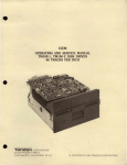
TM5U-l AND TM5U-2 THINLIN~TM
5-1/4-INCH fLEXIHLE DISK DRIV~S
48 TRACKS PER INCH
TAN DON CORPURATIUN
2U320 PRAIRIE STREET
CHATSWURTH, CALIfURNIA 91311
~CUPYRIGHT 1983 TANDUN CURPURATIUN
NOTICE
This document, and the information contained
herein, is copydC)ht by
Tandon
Corporation and may not be duplicated or repr.oduced, in whole
or in part, without the prior written approval of Tandon Corporation.
cletailec]
This
document
1S
intended
to provide
tilE:
user with
and
information adequate for the efficient installation, operation,
service of the equipment involved.
However,
while
every effort has
been made to keep the informati,on
contained herein
current and accurate as of the date of publication,
no C)uarantee
is given or implied as to its accuracy.
CONTENTS
Section
Number
'Ii tle
SECTION 1
GENERAL DESCRIPTION
Page
Number
1.4
1.5
Introduction •
Scope Of The Document
Purpose Of The Drive
Major Features
Write Protect
Daisy Chain Capability
Internal Trim Erase
Industry Standard Interface Compatibility
Track 0 Sensor •
Index Sensor . • .
Activity Indicator
Compact Size • •
Functional Description
Physical Description
SECTION 2
PRODUCT SPECI!"ICATIONS
2.1
2.2
2.3
2.4
Introduction .
...•..•.
Mechanical Specifications • . •
Electrical and Operational Specifications
Reliability Specifications
Environmental Specifications
SECTION 3
OPERATION
1.1
1.2
1.3
3.1
3.2
3.3
3.4
3.5
3.6
Introduction •
Unpacking The Drive
Preinstallation Checkout
Mounting The Drive
Dust Cover . • • •
Cooling
Interface Connections
Input Control Lines
Output Control Lines
Typical Interface Characteristics
D. C. Power .
. . . . .
Drive Address and Option Patching
DSO Through DS3 Jumpers
MX Jumper
. • • .
i
1-1
1-1
1-1
1-1
1-1
1-2
1-2
1-2
1-2
1-2
1-2
1-2
1-2
1-3
2-1
2-1
2-1
2-1
2-1
3-1
3-1
3-1
3-2
3-2
3-2
3-3
3-4
3-6
3-7
3-7
3-8
3-8
3-8
CONTI<;NTS
Section
Number
3.7
SECTION 4
4.1
4.2
4.3
Paye
Number
'Ii tle
Motor Select ,Jumper
Write Protect (WI)
Head Type (W2, W3)
W4 Through W8
Side Select (W9)
Motor On (WI)
Diskettes • • •
Loadiny The Diskette
Write Protect Tab
Diskette Handling and Storage
THEORY Of OPERATION
Introduction
Data Recording .
Components Of The Drive
Generate and Interpret Control Signals
Index Sensor
4.4
4.5
4.6
SECT ruN 5
5. 1
5.2
5.3
5.4
5.5
3-11
3-11
3-11
3-11
3-11
3-12
3-12
3-12
3-13
3-13
Write Protect Switch
Track 0 Sensor
Drive Select
Read/Write Head Positioner
Step and Direction
Stepper Motor Control
Stepper Motor.
Read/Write Data
Read/Write Head Assembly
Side Select Circuits
Write/Erase Circuits
Read Data Circuits
Spindle Control
. . • .
Spindle Motor and spindle Assembly
Spindle Motor Enable Circuit
Spindle Motor Control Circuit
Diskette Enabled Switch (Door Lever)
4-1
4-1
4-4
4-4
4-4
4-5
4-5
4-6
4-7
4-7
4-8
4-8
4-8
4-8
4-8
4-9
4-12
4-12
4-13
4-13
4-14
4-14
MAINTENANCE CHECKS AND ADJUSTMI<;NTS
Introduction
Visual Inspection
Equipment Required
Power Drive Select Check
Write Protect Switch Check and Adjustment
write Protect switch Check
Write Protect switch Adjustment • .
Drive Motor Speed Check and Adjustment
Drive Motor Check .
Drive Motor Adjustment
ii
5-1
5-1
5-2
5-3
5-4
5-4
5-4
5-4
5-4
5-5
Section
Number
5.6
5.7
5.8
5.9
5.10
5.11
5.12
5.13
SECTION 6
Title
Numbc} r
Radial Track Aliunment Check and Aejjustment
Radial Track Aliynment Check .
Radial Traok Aliynment Ad]ustmerlt
Index Checks and Adjustment
Index-To-J)ata Pulse Ctlecks
Index Sensor Adjuslment
Az i mu th Check .
Track 0 Sensor Check and Adjustment
Track 0 Sensor Check •
Track 0 Sensor Adjustment
Track 0 Stop Adjustment
Head Output Check .
Cone Centeriny Check
Compliance Check and Adjustment
(Single-Sided Drives)
Compliance Check .
Compliance Adjustment
5-6
5-7
5- i U
5-10
5- 11
5-13
5-13
5- l5
5-[5
';-16
5-l6
5- 17
5-1',)
5-2U
5- 2U
5- 2.l
REMOVAL AND INSTALLATION
Control and Data Circuit Board •
Servo Circuit Board
Chassis Shield, Control and Data Circuit Board
Diskette Lever Assembly
Front Panel
Power Input Fluy and Hracket
Write Protect Switch
Write Protect Sensor
Stepper Band .
Stepper Motor
Upper Plate Assembly
Track 0 Sensor and Track 0 stop \Ilock
Head Module
Drive Helt .
Drive Motor
6-2
6-2
6-3
6-3
6-)
6-5
6- 6
6-7
6-(j
6-1 U
6-12
6-14
6-16
6-17
6-18
APPENDIX A
Recommended Spare Parts and Major Assemblies
A-I
APPENDIX B
Circuit Board Schematics and Drawings
B-1
iii
ILLUSTRATIONS
Fi(:J ure
Number
1-1
2-1
3-1
3-2
3-3
3-4
3-5
3-6
4-1
4-2
4-3
4-4
4-5
4-6
4-7
4-8
4-9
4-10
5-1
5-2
5-3
5-4
5-5
5-6
5-7
5-8
5-9
5-10
5-11
5-12
5-13
5-14
6-1
6-2
6-3
6-4
6-5
6-6
6-7
6-8
6-9
Pagl~
Ti tle
Number
Disk Drive
Disk Drive Outline Drawing.
81ectrical Interface Characteristics
Control and Data Timing Requirements
Logic Board With Prograrrunable Shunts
and Option Patching Locations
Recording Media
Write Protect Tab • . • .
Diskette Care and Handling
81ectromagnetic Core .
PM Recording Magnetization Profiles
Read Timing Diagram
Interconnect Block Diagram
Soft Sectored Index Pulse
Track 0 Timing •
Write Data Circuit Block Diagram
Write Operation Timing Diagram
Read Circuit Block Diagram • • .
Servo Circuit Board
••
Logic Circuit Board With Test Points
Write Protect Switch Adjustment
Location Of R15 Speed Control Potentiometer
Bottom View Of Drive • • . .
Hub Center Line and Track Location . • • •
Cats Eye Patterns
Stepper Motor Retaining Screws and Camming Bars
Index-To-Data Pulse
••••
Index Sensor's Retaining Screw and Adjustment
uptimum Head Azimuth Alignment
Head Azimuth Alignment Of Acceptable
Lower Limits • .
. ..••.
Head Azimuth Alignment Of Acceptable
Upper Limits .
• •••
Track 0 stop .
• • •
Upper Arm and Compliance Spring
Control and Data Circuit Board
Servo Circuit Board
Diskette Lever Assembly
Power Input Plug and Bracket
Stepper Band •
Stepper Motor
• . • .
Upper Plate Assembly • • • •
Track 0 Sensor and Stop Block
Drive Motor
• • •
iv
1-4
2-2
3-7
3-')
3-10
3-12
3-13
3-14
4-1
4-2
4-2
4-3
4-5
4-6
4-10
4-11
4-13
4-14
5-2
5-5
5-6
5-6
5-7
5-8
5-10
5-11
5-12
5-14
5-14
5-15
5-18
5-21
6-4
6-4
6-4
6-5
6-10
6-11
6-13
6-15
6-19
TAHLES
Table
Number
2-1
2-2
2-3
3-1
3-2
Paye
Number
Title
Electrical and Operational Specifications
Reliability Specifications.
Environmental Specifications •
Drive Interface Lines and Pin Assiynments
D. C. Power Connector Pin Assignments
v
2-3
2-4
2-5
3-3
3-8
SECTION 1
GENERAL DESCRIPTION
INTRODUCTION
This document provides
required information
in order
and incorporate Tandon's disk drive into a system.
to
evaluate
Tandon Corporation's Model Number TMSO-l
and TMSO-2,
S-1/4-inch
flexible drives are compact, low profile drives that may be installed
in only one-half the space normally required.
They are compact data
storaye devices that use an ANSI-compatible, industry standard, 5-1/4inch diskette.
Model Number TMSO-l and TMSO-2 drives each 48 tracks per inch.
TM50-2 is a double-sided recording device.
The
Both drives
are
capable of
reading and writing in single-density
format on a diskette, using a proprietry read/write head patented by
Tandon.
The drives have a double density capability when a t10dified
Frequency Modulated (MFM) or other appropriate recording technique is
used.
Encoding
and
decoding
of
the
data
is
done by the
user's controller.
1.1
SCOPE OF THE DOCUMENT
This document
contains
the major features, physical and functional
specifications,
mounting and power requirements, the interface, and
typical timing characteristics of the TMSO-l and TMSO-2 drives.
In addition,
there
is a theory of operation, checks and adjustment
procedures, replacement procedures, assembly drawing~ and schematics.
1.2
PURPOSE OF THE DRIVE
The TMSO-l and TMSO-2 drives are rotating disk memories designed for
random
access
data entry,
storage, and retrieval applications.
Typical
applications
include
intelligent
terminal
controllers,
microcomputers,
word processing systems, data communication systems,
error logging, program loading, and point-of-sale terminals.
1.3
MAJOR FEATURES
write Protect
When a write protected diskette is inserted into the drive,
electronics are disabled.
1-1
the write
Daisy Chain Capability
The drive
provides
the address selection and gating functions
necessary to daisy chain a maximum of four units at the user's option.'
The last drive of the daisy chain terminates the interface.
The
terminations are accomplished by a resistor array plugged into a DIP
socket.
Internal Trim Erase
The drive provides
erasure of data.
the
control
signals
necessary for proper trim
Industry Standard Interface Compatibility
The drive is compatible with controllers that use an industry standard
interface.
Track 0 Sensor
The Track 0 sensor is provided to generate a logic level at the drive
interface,
indicating that the read/write head is positioned at the
outermost track.
Index Sensor
An index sensor is provided to generate electrical pulses at the drive
interface coincident with sensing Index/Sector holes on the diskette.
Activity Indicator
An activity indicator,
located on the front panel,
illuminated when the drive is selected.
is automatically
Compact Size
The reduced height of the drive enables it to occupy only one-half the
mounting space required for a conventional drive.
1.4
FUNCTIONAL DESCRIPTION
The drives are fUlly self-contained, and require no operator intervention during normal operation.
Each drive consists of a spindle drive
system, a head positioning system, and a read/write system.
1-2
When the front
latch is opened, access is provided for insertion of
a diskette.
The diskette is held in place by plastic guide rails.
Its
location is ensured when the diskette is inserted until a back
stop is encountered and the eJection mechanism latches.
Closing the
front
latch activates the cone clamping mechanism,
resulting in accurate centering and clamping of the diskette. The
drive hub is held at a constant speed of 300 RPM by a servo-controlled
D. C. motor.
The head(s) remain in contact with the recording media
until the front latch is opened.
The heads are positioned over the desired track by means of a fourphase stepper motor/band assembly and
its associated electronics.
This
positioner uses a one-step rotation to cause a one track linear
movement.
Data
recovery
electronics
include a
low-level read amplifier,
differentiator, zero crossover detector, and digitizing circuits.
No
data decoding capabilities are provided.
The drive has the following sensors:
1.5
°
1.
A Track
sensor detects when the head/carriage assembly is
positioned at Track O.
2.
An index sensor is positioned to generate a digital signal
when an index hole on the diskette is detected.
The index
sensor distinguishes index and sector holes in a hardsectored diskette.
3.
A write protect sensor disables the write electronics when
a write protect tab is applied to the diskette.
4.
A motor control switch.
PHYSICAL DESCRIPTION
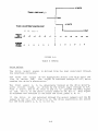
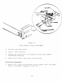
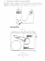
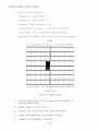
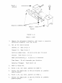
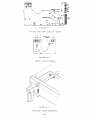
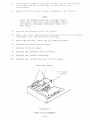
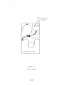
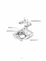
A representative drive is shown in Figure 1-1.
The drive can be
mounted in a vertical or horizontal plane.
However, the logic circuit
board
must be on the uppermost side when the drive is mounted
horizontally.
The spindle
is belt driven by a D.
tachometer.
The servo control circuit
speed of the spindle.
motor with an integral
C.
and tachometer control the
The read/write head assembly is positioned by a split band positioner
mounted to a stepper motor. The read/write heads are glass-bonded,
ferrite/ceramic structures with a life expectancy of 20,000 operating
hours.
Operator access for diskette loading is provided via a horizontal slot
located at the front of the drive.
The electronic components of
the drive are mounted on two printed
circuit boards.
The logic circuit board is mounted above the chassis.
The motorcontrol circuit board is mounted on the bottom of the
chassis.
Power and interface signals are routed through connectors
plugging directly into the logic circuit board.
1-3
FIGURE 1-1
D1SK DRIVe
I
I
I
I
I
I
I
I
I
I
I
I
I
I
I
I
I
I
I
I
I
I
I
I
I
I
I
I
I
I
I
I
I
I
I
I
I
I
I
I
I
I
I
I
I
I
I
SE:CTION 2
PRODUCT SPECIfICATIONS
INTRODUCTION
This section contains
the mechanical,
electrical and operational,
reliability, and environmental specifications
for the TM50-1 and
TM50-2 drives.
2.1
MECHANICAL SPECIfICATIONS
The physical dimensions of the drive are located in
Figure 2-1.
2.2
ELECTRICAL AND OPERATIONAL SPECIFICATIONS
The electrical and operational specifications are located
in Table 2-1.
2.3
RELIABILITY SPECIFICATIONS
The reliability specifications are located in Table 2-2.
2.4
ENVIRONMENTAL SPECIfICATIONS
The environmental specifications are located in Table 2-3.
TAN DON CORPORATION, CHATSWORTH, CALI fORNIA 91311
2-1
I
179[)[)[) 001
REV. A
!.6"f
"
(41.27MM)
m
~DI
•
8_00
."
1--
(203. 20 MM)
6-32
TAPPED
MOUNTlI'G
7.69
(l95.33MM)
HOLES
(2 PlCS
EACH SIDE)
J.i2!DI
3J2±..D1
l.e7~
Ul75
I ---_ e:=:======;::;:::::":j__ J
-_ .. _ - - - - - - - -
I
1.625
(4'1.27 MM)
- j
7.53
o
VIEW A (PC SA)
NOTES: 1. DIMENSIONS ARE GIVEN IN INCHES. METRIC EQUIVALENTS ARE IN PARENTHESES.
2. TOLERANCE ON ALL DIMENSIONS IS ±0.020 INCH, UNLESS OTHERWISE SPECIFIED.
3. WEIGHTIS APPROXIMATELY 3 POUNDS.
DISK DRIVE OUTLINE DRAWING
TAN DON CORPORATION, CHATSWORTH, CALIfORNIA 91311
2-2
17 ':1000-0 0 I
REV. A
TABLE 2 1
ELECTRICAL AND OPERATIONAL SPECIfICATIONS
Med ia
ANSI-compatible,
5-1/4-inch diskette
Media Life (for reference only)
4 X 10 6 passes per track
Tracks Per Inch
48 TPI, both drives
Tracks Per Drive
TM50-1
40 Tracks
TM50-2
80 Tracks
Track Spacing
0.529 millimeters,
20.8 milinches
Head Life
20,000 media contact hours
Disk Rotational Speed
300 RPM
Average Rotational Latency
100 milliseconds
Instantaneous Speed Variation (ISV)
~
Motor Start Time
One second, maximum
Seek Time, track to track
20 milliseconds
Fast Step Motor (Optional)
~
1.5 percent
3 percent
6 mi 11 iseconds
Head Settling Time
20 milliseconds
fast Step Motor (Optional)
15 milliseconds
Average Track Access Time,
including head settling time
287 millisecorlds
Fast Step Motor (Optional)
95 milliseconds
Typical Recording Modes
FM, MFM, MMfM
Data Transfer Rate
250,000 bits per second
double density
TAN DON CORPORATION, CHATSWORTH, CALIfORNIA 91311
2-3
I
179000-001
REV. A
TABLE 2-1 (CONTINUED)
ELECTRICAL AND OPERATIONAL SPECH'ICATIONS
Flux Reversals Per Inch (FRPI),
inside track
Both models, Side 0
5,535 FFPI
TM50-2, Side 1
5,877 FRPI
Unformatted Recording Capacity
TM50-1
250 kilobytes per disk
TM50-2
500 kilobytes per disk
D. C. Voltage and
Current Requirements
+5 volts D. C. Power
+5 volts + 0.25 volt at 800
milliamperes, maximum, with
less than 100 millivolts
peak-to-peak ripple.
+12 volts D. C. Power
+12 volts
~
0.6 volt, 1.3
amperes, maximum,
surge for
50 milliseconds, 800
milliamperes average.
Shipment
When prepared for shipment by
Tandon, the drive meets the
requirements of NSTA preshipment test procedure
Project lAo
TABLE 2-2
RELIABILITY SPECIFICATIONS
Error Rates, exclusive of
external sources, e. g.:
electronics, defective and
contaminated diskettes
Soft Errors (Recoverable)
One in 10 9 bits
Hard Errors (Nonrecoverable)
One in 10 12 bits
Seek Errors
One in 10 6 seeks
Mean Time Between Failures
Cl,OOO hours,
25 percent duty cycle
Mean Time To Repair
30 minutes
TANDON CORPORATION, CHATSWORTH, CALIFORNIA 91311
2-4
I
179DDD-001
REV. A
TABLE 2-3
ENVIRONMENTAL SPECIfICATIONS
Temperature
Operating, media dependent
Nonoperating
Relative Humidity
Operating, noncondensing,
media dependent
20-to-80 percent
Nonoperating, noncondensing
5-to-95 percent
Altitude
Operating or Nonoperating
152.4 meters, 500 feet, below sea level,
to 15,240 meters, 50,000 feet, above
sea level
TANVON CORPORATION, CHATSWORTH, CALIfORNIA 91311
2-5
I
179VDD 001
REV. A
SECTIUN 3
UPERATION
INTRODUCTION
This section contains
information on how to unpack,
stall, and operate the TM50-1 and TM50-2 drives.
3.1
check out,
in-
UNPACKING THE DRIVE
The drives are shipped
in
protective containers to
minimize
the
possibility of
damage during shipment.
The following list is the
recommended procedure for unpacking the drive.
1.
Place the container on a flat work surf ace,
top side up.
2.
Cut the tape that holds the tab in the slot on the front side
of the container.
CAUTION
Container may spri ng open when the tape
is cut.
3.
Remove the drive from its plastic bag.
4.
Inspect the drive for possible damage.
5.
Notify the carrier immediately if any damage is found.
6.
Save the shipping container for future use.
3.2
PREINSTALLATION CHECKOUT
Before applying
be conducted:
1.
power
to the drive,
the following inspection should
It
Check to ensure the front latch rotates easily.
should remain in the open position when rotated fully
counterclockwise (horizontal to front panel).
NOTE
When the latch is moved to an open position,
the head arm raises.
2.
Remove the cardboard shipping insert,
future shipment.
3.
Ensure the front panel is secure.
3-1
and retain for
4.
Ensu re the dr i ve be 1 t
5.
Manually rotate the drive hub.
6.
Ensure both circuit boards are secure.
7.
Ensure the connectors are firmly seated.
3.3
is 1n place.
It should rotate freely.
MOUNTING THE DRIVE
The drive has been designerl to be mounted horizontally or vertically.
When mounterl
horizontally, the logic circuit board side of the rlrive
must be the top side.
Tapped mounting holes are providerl on each side and the bottom of the
drive
for attachment to user-supplied mounting brackets (figure 2-11.
When
installed
in either plane,
horizontal
or vertical, only two
mounting screws are required to securely hold the drive in place.
Two drives may be mounted
in a single, full-size drive enclosure,
3.25-inches high.
A two-hole mounting scheme per drive is recommended
for mounting in a two rlrive configuration.
Any mounting
scheme
in which
the drive is part of the structural
integrity of the enclosure is not permitted.
Mounting schemes should
allow for adjustable
brackets or
incorporate resilient members to
accommodate
tolerances.
In arldition, it is recommended that mounting
schemes inclurle no more than two mounting surfaces.
The
testerl with some critical internal
rlrive
is manufactured and
alignments
that must be maintained.
Hence,
it is important that
mounting hardware not introduce significant stress on the chassis.
Dust Cover
The
design of
an enclosure should incorporate a means to prevent
contamination from
loose
items,
e. g.,
dust, lint, and paper chad
since the drive does not have a dust cover.
Cooling
Heat
dissipation from a single drive is normally 15 watts, 51 BTU per
When the drive is mounted so the
hour,
under high load conditions.
components
have
access
to a
free
flow of air, normal convection
cooling allows operation within the specified temperature range.
When
forced
ai r
is used, air flow must be directed outward from the
drive.
Do not intake air through the drive or ~eads and diskettes.
The
use of forced air flow is recommended when two drives are mounted
within a single enclosure.
3-2
3.4
INTERFACE CONNECTIONS
Interface connections
tor the TM50-1 and TM50-2 drives are made Vla
a user-supplied,
thirty-four pin, flat
ribbon connector,
3M Part
Number
3463-0001 or AMP
Part
Number
583717-5, using contact ParL
Number 1-583616-1
for
twisted
pair
or
its equivalent.
This
connector mates
directly
with the
circuit board connector at trw
rear of
the drive.
The D. C. power connector has four pins and is
located at
the rear of the drive.
The
interface description of
the connectors,
and the location of each one, is contained in this
section.
Interface
lines are
located
In Table 3-1.
I). C. power
connector pin assignments arc located in Table 3-2.
The signal wire harness should be of the flat ribbon or twisted pair
type,
26-to-28 gauge conductor, compatible with the connector to be
used.
The recommended cable length is ten feet maximum.
TABLE 3-1
DRIVE INTERFACE LINES AND PIN ASSIGNMENTS
Input Control Lines:
Controller-To-Disk Drive
Ground
I
3
5
9
11
13
15
17
19
21
23
31
Pin
-
Signal
2
4
6
10
12
14
16
18
20
22
24
32
Connector Clamp
Spare
Dri ve Select 3
Drive Select 0
Drive Select 1
Drive Select 2
Motor On
Direction Select
Step
Compos i te write Data
write Enable
Side Select
Output Control Lines:
Disk Drive-To-Controller
Ground
7
25
27
29
33
Pin
-
Signal
8
26
28
30
34
IndeX/Sector
Track 0
Write Protect
Composite Read Data
Connector Clamp
3-3
Input Control Lines
Drive select Lines
The Drive Select lines provide a means of selecting and deselecting a
drive.
These four lines select one of the four drives attached to the
controller.
When
the signal logic level is true (low), the drive electronics are
activated,
and
the drive is conditioned to respond to Step or Read/
Write
commands.
A Drive Select line must remain stable in the true
(low)
state until a Step or Read/write command is completed. When
the si<Jnal
line logic level is false (hiCJh), the input control lines
and output status lines are disabled.
The drive address is determined by a select shunt on the logic circuit
board.
Drive Select lines 0 through
3 provide a means of daisy
chaining
a maximum of four drives to a controller.
Only one can be
true
(low)
at a
time.
An undefined operation results if two or
more drives
are
assigned the
same address or if two or more Drive
Select lines are in the true (low) state simultaneously.
Motor On
When this signal
is
true (low), the drive motor accelerates to its
nominal speed of
300 RPM, and stabilizes at this speed in less than
one second.
When the signal line logic level goes false (high), the
drive
decelerates
to
a
stop.
This signal is not gated with
Drive Select.
Direction Select and Step Lines (Two Lines)
When
the
drive
is selected, a true (low) pulse on the Step line,
with a time duration greater than
200 nanoseconds, initiates
the
access
motion.
The direction of motion is determined by the logic
state of
the
Direction Select
line when a step pulse is issued.
The motion is toward the center of the disk if the Direction Select
line is in the true (low) state. The direction of motion is away from
the center of
the disk if the Direction Select line is in the false
(high) state.
the Direction Select line should be
ensu re
proper positioning,
stable at least 100 nanoseconds prior to issuing a corresponding step
pulse, and remain true (low) 100 nanoseconds after it.
To
The access motion is initiated on the trailing edge of the step pulse.
The time period between consecutive trailing edges of step pulses
should be at least 20 milliseconds.
3-4
The
drive electronics
conditions exists:
write enable
iynore
is true
step
pulses
1.
~he
2.
The direction select is false (high),
positioned at Track O.
3.
The drive is not selecterj.
when
one
of
three
(low).
and the head is
Composite Write Data
When
the
drive
is
selected,
this
interface line provides the bit
serial composite write
data pulses that control the switching of the
write
current
in
the
selected head.
The write electronics must be
conditioned for writing by the Write Enable line.
For each high-to-Iow transition on the Composite Write Data line, a
'[his causes a flux
flux change
is produced at the write head gap.
change to be recorded on the media.
When a
single-density
(FM) type encoding technique is used in which
data and clock form the combined Write Data signal, it is recommended
that
the repetition of the high-to-Iow transitions, while writing all
zeros,
be equal to one-half percent, and the repetition of the highto-low transitions,
when writing
all ones, be equal to the maximum
data rate, 250 kilohertz ~ 0.1 percent.
Host
controllers may
implement write precompensation circuits that
recognize worst
case patterns and adjust the write data waveform.
Al though a value cannot be spec i f ied for wri te precompensat ion, Tandon
suggests a value of
250
nanoseconds
for systems using MFM double
density recording format.
Write Enable
When this signal is true (low), the write electronics are prepared for
writing data and the read electronics are disabled.
This signal turns
on write
current
in
the selected read/write head.
Data is written
under the control of the Composite Write Data and Side Select input
lines.
When
the write
Enable
line
is
false
(high), all write
electronics are disabled.
When a write protected diskette is installed in a drive, the wri te
irrespective of
the
state of the Write
electronics are disabled,
Enable or Side Select lines.
Side Select, TM50-2
The Side Select
interface
line defines
diskette is used for information transfer.
3-5
which side of a two-sided
A fa Iso (hiljhl level on this line selects the read/wrile head on side
zero,
the
lower head, of the driv(~.
A true (low) level on this line
selects
the
read/write
head
on
side
one, the
upper hea.d, of
the drivG.
Output Control Lines
Index/Sector
'Lhe
index/seCl,)r
sector siiJnals.
signal
is
composite
of
the
index pulse and
index
pulse
is
provided once every revolution, 2UU millisecond~
nominal,
to indicate the heginning uf a trClck to the contcoller-.
Th(~
leadin!j
pdlJc
of
this
si.gnal
must
always he used to t?rlSLlre Liminid
accuracy_
'ftIP irldex/sector line remains in the true (low) state [c)r
the duration of ttle index pulse, which is nominally f()ur nlillisec()nds.
i\n
The sec lor
siljnal
sectored diskettes.
portion
appears
only
when
using
hard
Track 0
When
the
drive
is selected. the Track 0 interface siynal. when true
(low).
indicates
to
the
controller that the read/write head(s) are
positioned
at
Track
O.
This
siljnal remains true (low) until the
heads are moved from Track O.
Write Protect
When
the
Write
Protect
line goes true (low). the diskette is write
protected
and
the write electronics are disabled.
It is recommended
the controller not issue a Write command when the Write Protect siljnal
is true (low).
When
the
Write
are enabled.
Protect
line
is false
(high).
the
write electronics
Composite Read Data
This interface line transmits the readback data to the controller when
the
drive
is selected.
It provides a pulse for each flux transition
detected from the diskette.
The Composite Read Data output line
goes
true
(low)
for
a
duration
of
1 + 0.25 microseconds for each flux
chanlje detected from the diskette.
The
the
leadinlj
edlje
of the Composite Read Data output pulse represents
true
position of the flux transitions on the diskette's surface.
3-6
Typical Interface Characteristics
Lines
between
the
controller
and
the
drive
have
the
following
characte~istics:
+ 0.4 volt maximum at lout
Vout True
=
48 milliamperes,
maximum
Vout False
=
+2.4 volts minimum open collector at lout
250 microamperes, maximum
Figure 3-1 contains
Figure 3-2 contains
the
the
characteristics of the electrical interface.
control and data timing requirements.
+5 VOLTS
150 OHMS
,-------l
1
74LS040R
EQUIVALENT
+ TRUE
1
----1)c>-1'~=t±========~=;_1---q
+ TRUE _ _
'-I
~
I
I I
: 7438 OR
L ~~VALEN",:-
__
TRANSMISSION
LINE'" 1 0 FEET
J
RECEIVER
DRIVER
fIGURE 3-1
ELECTRICAL INTERFACE CHARACTERISTICS
3.5
D. C. POWER
D. C. power is supplied to this drive via a four-pin AMP connector,
J7, connected
to the
rear of the drive.
The mating connector, not
supplied, is AMP Part Number 1-480424-0, using At1P contact Part Number
606191-1.
Pin assignments are found in Table 3-2.
The
chassis
should
proper operation.
be
connected
3-7
to
earth
ground to ensure
TABLE 3-2
O. C. POWER CONNECTOR PIN
ASSIGNMENTS
Pin
1
2
3
4
Pin
Ground lug
3j16-inch
quick
disconnect
3.6
SUDDlv Voltaae
+ 12 volts O. C.
12 volts return
5 volts return
+5 volts o. C.
sillnal
Chassis ground from
controller
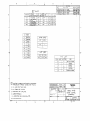
DRIVE ADDRESS AND OPTION PATCHING
The drive
address
and
option
patching
is
determined by the
programmable shunt, located at U19
on the logic circuit board.
The
DSO through TIS3 Jumpers determine the drive address.
The MX jumper is
used only in single drive systems.
Drive address and option patching
jumpers are located in Figure 3-3.
The
program shunt is AMP Part Number 435704-7.
The shunt positions
can be
cut using AMP's
tool, Part Number 435705.
The shunt is installed
in a DIP socket.
At the user's option, it can be removed and
replaced by a DIP switch.
OSO Through OS3 Jumpers
When daisy chaining
two or more drives to a controller, the Drive
Select
(DS) jumpers patch
the drive select control signal to enable
the logic of the proper drive.
Normally, all the shunt jumpers would
be cut, except for the DS jumper that addresses each individual drive
in
the
daisy
chain.
The
terminator pack, 2F, located on the
logic circuit
board should be
installed
in the last drive of the
daisy chain.
MX Jumper
The Multiplex
(MX) jumper
is
used only
in single drive systems
when the user
requires the drive logics to be enabled at all times.
I f the drive is not
selected through the OS jumper, and the MX jumper
is
not
cut,
the
drive
logics are enabled but the front panel
L. E. D. is
not
on.
The MX
Jumper must
be
cut
in
a multiple
drive system.
3-e
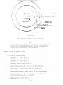
r - - - - - - - - - - - - - - . . . , ' , ...-,.- - POWER ON
--j
I
DRIVE SELECT
1 SECON 0
MINIMUM
- - - - - - - - -.......,
---
...-.
MOTOR ON
! :3-----------1
MILLISECONDS
I
r------2QO
250 MILLISECONDS---j
MAXIMUM
1
I
--.::.:=.::....----U
INOE':
f--4
~
TRACK
¢
I
500 NANOSECONDS
r- MAXI
MUM
I
r- 500 NANOSECONDS
WRITE PROTECT---------...:..-
DIRECT ION
MILLiSECONDS
-...,',.......
"
_"_A_X_'"_U_"
I
------------.;-'II
MIN IMUM
I
r-
NANOSECONDS
MINIMUM
i'~
~
I
I
NANOSECONDS~
MINIMUM
I
l-
::f-=-
..-' ..., , - - u
~
~
I
40MILL1SECONOS
I
MAX/MUM . . . --
-----------;-r-----~r-5-0-"-'-L-L-'-SE-C-O-N-D-S
~
.
MIN IMUM
I
200 NANOSECONDS -MINIMUM
390
-------!----.---
r- r-4
1-1
ui.riJ u -
Io-~ 4 MICROSECONDS
r
--1
8 MICROSECONDS
MICROSECONDS
--uuu~"
250 MILLISECONDS~
MINIMUM
}
B MICROSECONDS
NOTES,
I
"'=j., L~
12100 NANOSECONDS
MINIMUM
READ DATA
M(CROSECONOS~
MICROSECONOS~ I
-----------+:"'M"A:;,X""M"'U"M"-100 MICROSECONDS "I
Jr-----
•
900
I
WR 11£ DATA
l-
100 NANOSECONDS~
"'N'"U"
L.JU
100
ERASE GATE
(TUNNEL ERASE)
_
,J
1100
200 'NANOSECONDS
STEP
_
...... '.1
1L
20MILLISECONDS--1
MINIMUM*,,,
WR ITE GATE
.,
_ _ _ _ _ _ _ _ _...:..--,
Ll
SlOE SELECT
,
~
l
~ ~1
MICROSECOND
NANOSECONDS
FOR REFERENCE ONLY
6 MILLISECONDS FOR FAST STEP MOTOR (OPTIONAL)
21 MILLISECONDS FOR FAST STEP MOTOR (OPTIONAL)
FIGURE 3-2
CONTROL AND DATA TIMING REQUIREMENTS
3-9
±
250
o
-- -.,
3!!_e_1
----,
!....
, .,
$"
3
U19
NOT USED
-"
3
0
16
2
DSO
15
3
OS I
14
4
DS2
13
5
OS 3
12
6
MX
11
7
NOT USED
10
8
MTR SEL
9
~
FIGURE 3-3
LOGIC BOARD WITH PROGRAMMABLE SHUNTS AND OPTION PATCHING LOCATIONS
3-10
Motor Select Jumper
The Motor Select jumper, MTl' Sf~L, should be connected when the spindle
motor is to be turned on using Drive Select or Motor On Control
lines.
NOTE
The following jumpers are located on the read/write
can t ro 1 boa rd.
x
=
=
Connected
Not Connected
Write Protect (Wl)
The standard write protect feature
control is inhibited with Wl installed.
is
wl removed.
Write protect
write Protect
wl
wri te Protect control, in response to a wri te
protected diskette, inhibits Write Gate, thus
disallowing the flow of write data to the
read/write heads.
x
write Protect Control is inhibited.
Head Type (W2, W3)
This option selects the type of head used.
w2
W3
Head Type
x
Tunnel erase.
x
Straddle erase (optional).
W4 Through W8
W4 through W8 are not used.
Side Select (W9)
For use in double-sided drives.
W9
Side Select
x
For use in single-sided drives, TM5U-l.
For use in double-sided drives, TM50-2.
NOTE
The following jumper is located on the motor control board.
3-11
Motor Un (WI)
The standard
motor.
The
is installed.
3.7
operation has
a Motor Un signal controlling the drive
drive motor can be controlled by Drive Select when WI
WI
Motor Is Controlled By
x
Motor Un J8-16.
Motor Un or Drive Selected.
DISKETTES
The TM50-1 and TM50-2 drives use an ANSI-compatible
5-1/4-inch
diskette.
Diskettes are available with a single
index hole or
with multiple (index and sector) holes.
Diskettes
with
a
single hole are used when soft sector format
is
required.
Multiple hole diskettes provide sector information
through the use of an
index sensor and electronics.
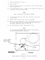
Figure
3-4 contains the diskette used with the drive.
This recording
media is a flexible diskette enclosed in a protective jacket.
The
protected diskette, free to rotate within the jacket, is continuously
cleaned by its soft fabric lining during normal operation.
Loading The Diskette
The
drive
is
loaded by inserting the diskette,
head aperture
forward,
into the front slot of the drive.
Access to the diskette
loading slot is obtained by opening the front latch.
The diskette should be carefully inserted until it is solidly against
the back stop.
3.S6 MM
(0.14 INCH)
~
I,
r-
I
i
I
i"--c---+l, =4
I,
1 33,4 MM
(5.25lNCHl
L
-1--«
o
I
I
l-
SEALED
):1--+
r
6.30 - 0.25 MM
(0.25 ,- 0.01 INCH)
96,5 , 0.25 MM
(3.BO ~ 0.01 lNOH
rL..'±'..-l'---J~
I
13J,4MM
(5.25 INCH)
133.4 MM
(525INCH)
~
--1
II
PROTECTIVE
JACKET
SPINDLE
ACCESS HOLE
HEAD
APERTURE
FIGURe; 3-4
RECORDING MEDIA
3-12
CAUTION
Damage to the center of the diskette may result if the door
is closed when the diskette is not properly inserted.
This prevents reliable recovery of recorded data.
write Protect Tab
The drive
is equipped with a write protect sensor assembly.
This
sensor operates
in conjunction with a diskette that has a slot cut in
the protective jacket.
When the slot
is covered with an optically opaque, self-adhesive
tab,
the diskette
is write protected.
The tab must be removed to
write on
the diskette.
Figure 3-5 contains information on how to
install a tab to cover the slot.
Diskette Handling and
~torage
It
is
important the diskette be handled and stored correctly so the
A damaged or contaminaintegrity of the recorded data is maintained.
ted diskette
can
impair or prevent recovery of data, and can result
in damage to the read/write heads.
Figure 3-5 contains an
illustration of the physical configuration of
the diskette.
The
5.125-inch diskette is oxide-coated,
flexible
mylar.
It is enclosed in a
5-1/4-inch square protective jacket.
In addition,
openings
for
the
drive hub and diskette index
hole are provided.
WRITE PROTECT TAS
\
~
@
o
'-
0
FOLD OVER BACK OF DISKETTE
r
3.56 MM
(O.14INCH)
6,30 MM
,-----+i~(O.25INCH)
r
r;:=:::,
Q;
o
0\
~_-y
98.5MM
(3.B08INCHES)
l
INDEX ACCESS HOLE"":'
FIGURE 3-5
WRITE PROTECT TAB
3-13
WRITE PROTECT TAS
figure 3-6 provides
some helpful
hints
on the care ann handling of
the
drive .and diskettes.
In addition,
to ensure
trouble-free
operation and to enhance the service life (yE the di.c;kett_8, the f()L Lo\..;in<J han i Litli] prucedu res ShOll ld be observed.
DO NOT WRITE ON THE
JACKET WITH PEN OR
PENCil. USE A FELT
TIPPED PEN.
TO AVOID DAMAGE TO
THE DISKETTE AND TO
YOUR DRIVE, INSERT
DISKETTE CAREFULLY
UNTIL THE BACKSTOP
is ENCOUNTERED.
DO NOT TOUCH PRECISiON SURFACE WiTH
YOUR FINGERS.
KEEP THE DiSKETTE
AWAY
FROM
MAGNETIC FiELDS.
DISKETTES SHOULD
BE STORED AT
1 O"C to S2'G
50"F to 1 25°F
RETURN THE DISKETTE
TO ITS JACKET WHEN
NOT iN USE
HANDLE WITH CARE;
BENDING AND FOLD,
ING
MAY
DAMAGE
DISKETTE.
FIGUNE 3-6
DISK":TTE CARE AND HANDLING
1.
Return the diskette to the protective jacket when not in use.
2.
Avoid exposing the diskette to any magnetizing force in
excess of 50 oersted.
Note
The 50-oersted level magnetizing force is reach=d at a
distance of approximately three inches from a typical source,
e. g., motors, generators, or transformers.
3.
To avoid warping, do not store the diskette in
direct sunlight.
4.
])0
not use a lead pencil or a ballpoint pen to wri te on the
Use a felt tipped pen, and mark lightly on the label.
labe 1.
3-14
SI'CTION 4
THEORY OF OPERATION
INTRODUCTION
This section contains a description on the theory of operation of the
drive.
The discussion begins with a general suwnary of magnetic data
recording,
followed by a description of each major function of the
drive.
Circuit block diagrams and schematics are located in the appendices.
They are useful to show the interconnections between the electronic
circuits and the mechanical components.
4.1
DATA RECORDING
Digital
information is
represented by a sequence of bits:
either
o or 1. Small areas of the medium in which such binary information is
stored,
for example the iron oxide coating of a magnetic disk, must
be put in one state or the other to represent the data.
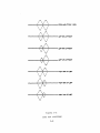
Recording of data on a magnetic medium is based on the principles
of electromagnetics.
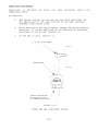
When current flows in a coil of wire it produces
a magnetic field.
The field is confined
in a core of magnetic
material around which the wire is wound. A narrow slot, called the
air
gap,
is placed in the core located closest to the media.
It
is the magnetic field in the vicinity of the air gap that magnetizes
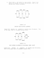
the magnetic medium (Figure 4-1). When the current is reversed, the
polarity of magnetization is reversed.
Information can be recorded on the diskette by using a doublefrequency
code.
The magnetization profiles in each bit cell for the
number sequence shown for FM recording are shown in Figure 4-2.
The
When data is read, the same head that writes the data is used.
In each bit cell,
data stored is a digital bit representing a a or 1.
the first flux
reversal represents a clock bit. A second reversal
stored
bit
1.
The absence pf a second reversal
represents a
represents a bit O.
/ " " " - - - - ELECTROMAGNETIC CORE
MAGNETIC FIELD OF HEAD
ELECTRIC
CURRENT
----~...:::_-4..J
MAGNETIC FIELD OF MEDIA
~
•
ROTATION OF MEDIA
FIGURE 4-1
ELECTROMAGNETIC CORE
4-1
--lIlT caulIITPATTPN
I
I
I
I
I
I
I
I
I
I
I
I
I
I
f
I
I
WIIITBDATA
I
I
I
I
I
I
I
I
I
I
1
I
I
I
I,
I
I
I
I
I
I
I,
,I
HHlfl~nl;jIYo
j
IIIAGNrnzATlON:::::A
I
IIIAGNETlC .......NT8
U
I
U
I fI
NN 55 NIN
5
I
I
I
I
I
I
I
I
I
I
I
I
,
I
01
~
I
h
I
I
I
,
I
I
I
5~N
I
I
I
I
I
I
I
I
I
I
I
q
55 N ' B S J ' ; r N
I
I
I
I
I
I
I
I
I
1
I
I
I
I
IL
I
I
:
53U
I
I
,
I
I
,
I
I
I
FIGURE 4-2
FM RECORDING MAGNETIZATION PROFILES
As the disk spins,
the magnetic fields of
the stored data pass
successively under the head.
The changing fields induce, in the head,
an A.
C.
voltage signal which
is
then amplified and filtered,
differentiated, and digitized (Figure 4-3).
The comparator and the digitizer circuitry generate a one microsecond
Read Data pulse, corresponding to each peak of the Read signal.
Then,
the composite read data signal is sent to the user system via the Read
Data interface line.
UN.... OUTPUT 1'110101 PlLTIJI
OUTl'UT 1'110101 DII'PIIIINnATO"
I
I
II
I,
u---u-
liDO DATA INTIJIL"ACI
I
I
fIGURE 4-3
READ TIMING DIAGRAM
4-2
I
I
HEJI.D 0
P6
HEAD 1
36
P5
CON":POL AND
READ/WRITE
CIRCUIT BOARD
INDEX
SENSOR
INDEX
EMITTER
P12
312
(1-4)
Pll
nl
( 1-2)
~ PI0
310
(1-6\
WRITE
PROTECT
A,
I~
a(1.~
,
.: .,
.."
,
:-'r::Tr'::,Q,
Cll;.JTROL
lNTP<F.'\CF
La-
0
0
/0)
...L
I--
INDEX
P9
TRACK
ZERO
DETECTOR
I/O
INTF:RFACE
38
11-3")
,T9
(l-4 )
D.C. DRIVE
MOTOR
P
~ '"~I+-
.... -+
P7
37
(1-4 )
?O\,<'E!"
':2NNETTOR
11-4 )
SPINDLE
MOTOR
-+
STEPPER MOTOR
CONTROL
4
DISKETTE LOADED
Pl
31
(1-4 )
P2
32
(1-4)
P3
33
(1-6)
P~
34
(1-6)
P5
J5
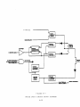
FIGURE 4-4
INTERCONNECT BLOCK DIAGRA11
4-3
ACTIVITY::
IeI'D
DRIVE MOTOR
SERVO
CIRCUIT
BOARD
(1-2)
t::::t..1
-- - - - - - - - - - - - -
4.2
CUMPUNENTS Uf THE DRIVE
The drive contains the electrical and mechanical components required
to perform four major functions:
1.
(;enerate and interpret control signals.
2.
Position the read/write head(s)
3.
Write and read data.
4.
Control the spindle.
to the desired track.
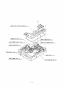
The electrical and mechanical components of the drive are connected
together via multiple pin connectors.
This allows the individual
assemblies to be removed (figure 4-4).
4.3
GENERATE AND INTERPRET CONTROL SIGNALS
The components
of
control signal are:
the
drive required to generate and interpret the
1.
Index Sensor
2.
Write Protect Switch
3.
Track 0 Sensor
4.
Drive Select
Index Sensor
The
Index signal
is derived from an infrared L. E. D. and phototransistor detector.
When the
index/sector hole
in the diskette
passes
through the
index sensor,
the
light
from the L. E. D. is
allowed to turn on the index detector, producing a positive pulse on
J12, Pin 4 (Figure 4-5).
This signal is shaped by an input buffer, U9, and supplied LO inverter
IC U17.
Then
it
is gated with Drive Select for an output control
signal at the interface J8, Pin 8.
4-4
nsTPo,NT7-nl....------1L
1.-4 MIWaCONDS AV!IIAGI
~-------200MILUaCONDS--------I-l
FIGURE 4-5
SOfT SECTORED
INIJEX PIJLSE
Write Protect Switch
The
Write
Protect
signal
is
derived
from
a
mechanical
switch
integrated
into
the drive, the switch is deactivated, causing a high
signal
on
,Jll,
Pin 5.
Then, it is buffered and inverted to disable
the
Write
Enable
signal.
It
is
also gated
with
drive select,
producing an output signal on the interface.
Track 0 Sensor
The Track
0
sensor
signal is derived from an infrared L. E. D. and
phototransistor
internal
to
the
drive.
As the head carriage moves
back toward Track 0, the sensor is activated between Tracks 0 and 2.
This
low active
signal
comes
in via J~, Pin 4.
It is inverted by
IC
U~.
The combination of the Track 0 sensor being activated and the
proper stepper motor phase (Phase 0) produces a low output at IC UH,
Pin 6 (Test Point 10).
This signal is buffered through IC U17, Pins ~
and H, to be gated with drive select at IC UlH, Pins ~ and 10, to give
a
Track
0 output
to Pin 26 of the interface.
After IC U17, Pin R,
this
signal is gated with direction (IC U7, Pin 12) at Ie U6, Pins 12
and 13.
IC U6,
Pin II,
when true low inhibits stepping to Track 0 mInus 1.
4-5
r - - - - - - - - - + I VOLTS
'nIACK 0, TaT I"OIMT
10
_ _ _...J 0 VOLT
I
I
I
I
Tl\AC:K 0 AD.JUSTHIINT MONITQR POINT
- - - - - - - - - 0 VOLT
Ie U8, PIN 4
TltACKS
ON
1liSKITT1!
-.
-I
--
-3
0
1
-2
-1
0
1
o
+1
+2
+3+4+1+1
1
o
1
I
I
I
,TIPPeR
MarcH
PHAAS
+5 VOLTS
0
o
1
a
1
a
FIGURE 4-6
TRACK 0 TIMING
Drive Select
The Drive Select signal is derived from the host controller through
the interface connector.
R39 holds
the output of the appropriate select line high until the
line
is driven
low.
The
signal is buffered through IC U17, which
enables the drive's electronics.
front
panel
L.
E. D., physically located on the drive motor's,
The
is driven by the select logic through IC U17,
servo circuit board,
Pins 5 and 6, and Ie U7, Pins 11 and 10, to provide the NSEL signal
pin 5, to the servo circuit board on J4, Pin 5.
This signal
at JIO,
is buffered and inverted to activate the front panel L. E. D.
If
the drive
is
not selected through the select jumpers and the MX
jumper is not cut, U19, Pins 6 to 11, the drive electronics are active
but the front panel L. E. D. is not on.
4-6
4.4
READ/WRITE HEAD PUSITIONER
The components of the drive required to position the read/write
head(s) at the desired track are:
1.
Step and direction circuits
2.
Stepper motor control circuits
3.
Stepper motor
Step and Direction
The Step and Direction signals are derived from the host controller
via interface connector J8, Pin 20, and J8, Pin 18, respectively.
The
direction line is buffered and inverted on the control and
read/write circuit board and sent to the motor control circuit board
via JIO, Pin 1. On the motor control circuit board, it is used as the
D input of IC U6, Pin 12, the direction flip-flop;
The
step
pulses
are buffered by IC U17, Pins 1 and 2, and gated
with Drive Select at IC U8, Pins" and 10.
IC U8, Pin 8, is inverted
by IC U7, Pins 1 and 2. Test Point 11 can be used to monitor the step
input, which is output at JIO, Pin 3, to the motor control circuit
board.
On the motor control circuit board, the step pulses are used to clock
the direction flip flop IC U6 at Pin 11 and the step one shot flip
flop (time is two microseconds) at IC U8, Pin 10.
Generation of controlling signals for correct stepping phases is
accomplished via IC U7.
The direction flip flop controls the up or
down counting of
the step pulses (two pulses per track) used by IC
U7.
IC U8,
Pin 12, when clocked by a step pulse will clock IC U7 at Pin
14,
thus Pin 3 of IC U7 wi 11 trigger a 10-mi 11 isecond one shot at IC
U8, Pin 2, which retriggers the two microsecond step flip flop IC U8,
Pin 9.
IC U7 is clocked again to complete a single phase rotation of
the stepper motor through logic driver IC's Ul and U2.
NOTES
THE TIMES IN THE ABOVE DESCRIPTIUN ARE fUR THE
20-MILLISECOND STEPPER MOTOR.
FOR ADDITIONAL
INFORMATION, SEE TABLE 1, SHEET 1 OF 3, MUTOR
CONTROL SCHEMATICS FOR COMPONENT VALUES AND
CHANGES fOR SIX-MILLISECOND STEPPER MUTORS.
PHASE 0 Of THE STEPPER MOTOR IS ACTIVE ON ALL
EVEN TRACKS: 0, 2, 4, 6.
4-7
Stepper Motor Control
The stepper motor control circuits generate the two phases of tile step
se4Llence
based
on
information
from
tho step and direction inputs.
These
tVJO
f:Jhases are fed to the stepp(~r motor drivers, which IH-oduce
the current through the motor's coils.
Stepper Motor
The stepper motor is a sinyle phase motor, which rotates 3.6 degrees
for each phase.
The capstan and split band translates this rotation
to a one track linear movement of the head carria(je assembly.
4.5
READ/WRITE DATA
The components of the drive required to read and write data are:
1.
Read/Write Head Assembly
2.
Side Select circuits
3.
Write/Erase circuits
4.
Read Data circuits
Read/Write Head Assembly
The
read/write head(s) are 'llass bonded, ferrite cores mounted
in
a ceramic structure.
The lower head structure is mounted in a fixed
position to a
plastic carriage.
The
upper
head is mounted to a
'limballed flexure to conform to the diskette.
The head carriage assembly is attached to the chassis on 'luide rails.
It is positioned by a split band attached to the stepper motor.
Side Select Circuits
The Side Select si'lnal
is derived from the host controller via the
interface connector J8,
Pin
32.
This si'lnal is buffered.
I f the
signal is
high
at
the
interface, Side U is selected by applyin'l
on the center tap of Head U, and allows current
a
volta'le potential
to
flow in
the
coils of Head U.
If the signal at the interface is
low, Side I 1S selected by applying a volta'le potential on the center
tap of Head 1, allowin'l current to flow in the coils of Head 1.
4-8
In the
read mode,
a potential of +5 volts D. C. is applied to the
selected head diode matrix.
The write mode increases the voltage
applied LO the
selected head diode matrix to +12 volts D. C. from
the beginning of Write Enable until the end of Internal Write Busy.
write/Erase Circuits
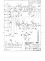
The
write
waveform
electronics
generator,
consist
an
of
a
write current source, a write
erase current source,
the trim erase control
logic, and the side select logic (Figure 4-7).
The signals required
host controller are:
1.
Drive Select
2.
Wri te Enable
3.
\vrite Data
4.
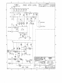
Side Select
to control the data electronics provided by the
The winding on
the head is center tapped.
During a write operation,
current from the write current Source flows in alternate halves of the
winding, under control of the write waveform generator.
When the drive is selected and write protect is false, N Write Enable
initiates the write
logic.
Seven events that occur are (Figures 4-7
and 4-8):
1.
The pre-erase delay one shot is started, 390 microseconds.
2.
The post-erase delay one shot is started, 900 microseconds.
3.
The post-erase delay one shot outputs a signal:
N Internal
Write Busy.
It is used to disable the Read Data output
circuit, NWRT to increase the read/write diode matrix voltage
from 5 volts D. C. to 12 volts D. C. via the side select
logic during a write operation.
4.
The write current source is enabled via U4.
5.
The write waveform generator has its preset and clear inputs
set to +5 volts D. C. instead of ground (optional).
6.
Input diodes to the read amplifier are reverse biased by
N write to protect the read amplifier during the
write operation.
7.
The write data input is inverted and used to clock the
waveform generator which selects a write driver, thus
providing a ground to forward bias a diode, allowing current
to flow through the coil.
4-9
N WRITE
L
I
SIDI
SlLICT
LOGIC
SIDISlLeCT
aU1'P1Il
NWIl.,.. DATA
~
_'--....
C
,....
Iwll.,..
~:YIJlOll~Il
INIIlATO
/
~
-
WIl.,..
DIlIV1Il1
~
wIlm
DIlIYIIl2
r"'II
)IlIADI
WIlITII
COiLa
-<
,r......
-<J
.....
,-
NWIl.,.. INAaLI
NWIl.,.. PllonCTr_
DIlIYI SILeCTf _
IN WRITII)
J
-< 11IM
-
,
-< COIL
-<
....
WIl.,..
CUIllllHT
SOUIlCI
-... ~
r
IIlASl
CUIlRINT
SOUIlCI
IIlASl
DILAY
LOGIC
IN INTIIlNAL _
WIlmausy)
FIGURE 4-7
WRITE DATA CIRCUIT BLOCK DIAGRAM
4-10
RIADDISAa LII
H01'I! 1
I
I
I
WIlITW IIIAILa
1
I
I
I
I
I
NOT1I21
I
I
I
I
I
I
I
310'
I
MICIlOSlCONDI...-j
TIlIM IRAII
I
I
I
IOD MICIlOSlCONDI--t
I
I--
-1--_.....:..---4~1
I
I
I
I
I
I
I
r'------i'--;.-..,...---..l.'---..,...--...l'----l--.J
I
I
I
I
I
I
:
I
INTIRNAL
WIIITWIUIV
I
1
NWIlITW DAT.\--t----i .----1
_-+
I
I
---r
I
I
I
I
NOTII2
WIlITW
WAVI!J'OIIM
QDIRATOIl
I
I
I
~
---6---"';"'-
----I
WIIITW CUIlIlIHT
IU--~
I
I
I
I
I
NOTII4
I-
I
I
IIOT'!S: 1. I- 0 - UO MIWSlCONDI AI"TD DillY. MOTOIl STAIITS 011 20 MIUISICONDI AI"TD LAST lTV PU.....
WHICHIVIR.I TH. LArlSTTl..L
2. UNSVNCHIIONID"
3. La MIWA....1R E S III!AK TO ..lAIC. •
4. 4 MICIlOSlCONDI MINI..UM, • MICIlOSlCONDI MAXIMUM
FIGURE 4-8
WRITE OPERATION TIMING DIAGRAM
4-11
When there
is a pre-erase delay 390-microsecond time out, the erase
current source is turned on.
The clocking of the waveform generator during write operation provides
a trigger to the post-erase delay one shot, and does not allow it to
time out until all data is written.
N Internal Write Busy is active until the end of the post-erase delay,
and keeps +12 volts D. C. on the read/write diode matrix during the
erase time.
The duration of a write operation is from the true going edge of write
Enable to the false going edge of Trim Erase. This is indicated by
the Internal Write Busy waveform (figure 4-8).
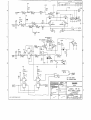
Read Data circuits
The read electronics consist of:
1.
Read Only and Side Select circuits
2.
Read Amplifier and Linear Phase Filter
3.
Differentiator
4.
Comparator, Time Domain Filter, and Digitizer
The Read Only circuits are used to isolate the read amplifier from the
voltage
excursion
across the head during a write operation. The
side select is used to enable one of the read/write head(s).
The drive must be selected by the user's system before reading can
begin.
In addition to the requirements established in this section, a
100 microsecond delay must exist from the trailing edge of the Trim
Erase signal to allow the read
amplifier to settle after the
transient caused by the Read Only circuit returning to the Read
mode.
The output signal from the read/write head is amplified by a read
amplifier, and filtered by a linear phase filter to remove noise.
The linear output from the filter is passed to the differentiator,
which
generates
a waveform whose zero crossovers correspond to
the peaks of the Read signal.
Then,
this signal is fed to the
comparator, time domain filter, and digitizer circuitry (Figure 4-9).
4.6
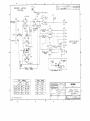
SPINDLE CUNTROL
The components of the drive required to control the spindle are:
1.
Spindle Motor and Spindle Assembly
2.
Spindle Motor Enable circuit
3.
Spindle Motor Control circuit
4.
Diskette Enable Switch
4-12
Spindle Motor ana Spindle Assembly
The Spindle Assembly is driven by a belt attached between two pulleys.
The
drive motor pulley
is turned by a D. C. motor with a built in
integra~ tachometer.
The spindle pulley connects to a hub that
rotates a clamped diskette.
Spindle Motor Enable Circuit
The Motor On signal is derived from the host
face connector via J8, Pin 16. This signal
to the servo circuit board, which uses it to
circuit of the spindle motor control via JIO,
U....mfHDD
TM50-2,
OfILY
-
->..
_
LOWmf
HDD
RDD OfILY
AND SIDI SlLlCT
CIRCUITS
.....
TOTJIOINT
,.
Dll'l'IRlHTlAlOR
TUTJIOIHT
4
%lRO CROSSOYmf
DInClOR
(COM..ARATOR'
.
4
DIGITlDR
r
~tTlSTJIOIHT
...
RDD AM"Ul'lmf
ANDUNDR
"NASI! I'lLTmt
..
~
...
TlMIDOMAIN
"'LUR
7
TEST POINT 9
.
•
~ TUTPOIHT
.~
6
f ...
~
controller to the interis buffered and supplied
enable the motor current
Pin 6.
DATA OUTJlUT
•,..
DRIVISlUCT
FIGURE 4-9
READ CIRCUIT BLOCK DIAGRAM
4-13
r--
4
5
Spindle Motor Control Circuit
The Spindle Motor Enable signal is input via J4, Pin 6, of the motor
control circuit board to gate the spindle motor current (Figure 4-10).
This current is controlled by an integrated regulator circuit when the
spindle motor is enabled.
The potentiator provides an adjustable
D. C.
voltage reference to the regulator circuit for spindle speed
adjustment.
The tachometer signal provides feedback from the motor
via Pins 3 and 4 of Jl of the motor control circuit board to maintain
a constant speed of 300 RPM.
This signal is 12 volts A. C.
Diskette Enabled Switch (Door Lever)
with power applied to the drive unit and the motor enable false,
inserting a diskette into the drive and closing the door lever turns
on the
motor for five seconds.
This feature ensures the proper
clamping of the diskette to the spindle hub and the centering cone.
Motor control can be accomplished by drive select with WI installed.
\
/
/
ZZ
H
H
P< P<
SPINDLE SPEED CONTROL
FIGURE 4-10
SERVO CIRCUIT BOARD
4-14
Itn;;J[~
PIN 6
SIo:CTION 5
MAINTENANCE CHIo:CKS AND ADJUSTMENTS
INTRODUCTION
This section is for the use of the OEM Repair and Service Departments.
It contains the maintenance checks and adjustments used during the
normal
life of the drive.
The purpose of this section is to outline
the steps necessary to verify the operation of the drive during
troubleshooting, or after replacing a part or assembly.
If a fault
is suspected with a drive,
following the checks and
adjustments
in the order presented will help to isolate the problem
area.
However,
if a specific check and adjustment is required, the
preceding checks do not necessarily need to be performed.
The values and tolerances stated in the checks and adjustments are
typical values for working drives.
If the values measured are within
tolerances or close to the limits, the suspected fault is normally
caused by some other problem.
Completing other checks and adjustments
may disclose the actual problem.
Refer to the schematics in the appendices and the theory of operation
in Section 4 for circuit descriptions.
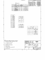
Test point location is
illustrated in Figure 5-1.
5.1
VISUAL INSPECTION
Before
applying power to the drive,
adjustments, visually inspect the drive:
or
doing
any
checks
or
1.
Check for loose or missing hardware.
2.
Ensure the front latch opens and closes.
when the door is opened.
3.
Ensure the front panel is secure.
4.
Manually rotate the drive hub.
5.
Ensure the circuit boards are secure.
6.
Ensure the connectors are firmly seated, and
installed correctly.
7.
Check for damaged or missing components on the circuit boards.
8.
Ensure that a diskette can be inserted and removed easily.
5-1
The head arm raises
It should rotate freely.
TM50 TEST POl NTS
12.
3.
4.
5.
6.
7.
B.
+12 volts D. C.
Write Protect Switch
Motor On (From Interface)
Read (A. C.)
Read (A. C.)
Read (Differential)
Read (Differential)
Ground
Read Data To Interface
Track Zero
Step
Index
Select
Ground
9.
10.
11.
12.
13.
14.
o
tnxDl.nClf WU'tOI
,.-a:
0
WI
;_1
-
rll-
rI'
rl2
PIOiOlMGIAILl S1IDIIT
rI'•
rI'
•
• rl7
• riO
.~
W2
w.;,
• rI.
0
1:4
l!_t
rl14
.-,
;.:
W?~t !Pll
rll'
.- rl12
riD
•
~~.
•••
:.'
W1'
0
I'"
r'IGURE 5-1
LOGIC CIRCUIT HOARD WITH TEST POINTS
5.2
EQUIPMENT REQUIRED
The following equipment is required for checks and adjustments.
1.
A duaL-channel, wideband oscilloscope, Hewlett Packard Model
1740A or equivalent.
2.
An exerciser, AVA Model 103C or equivalent, or a software
routine capable of stepping the drive to any track, selecting
the upper or lower head, and writing a IF, all zeros in FM,
or 2F, all ones in FM, pattern.
5-2
3.
A power supply.
4.
A certified alignment diskette, Dysan Model 224/2A
or equivalent.
5.
A certified output diskette, write protected,
104/2D with tab or equivalent.
6.
A certified output diskette,
Model 104/2U or equivalent.
7.
Associated power and interface cables.
8.
A number 1 Phillips screwdriver.
9.
Jeweler Screwdriver (speed adJust)
Dysan Model
nonwrite protected,
10.
Spring inserter/remover
11.
A flat blade screwdriver 3/16-inch tip.
Uysan
Test equipment must be in calibration.
This may be verified by
observing the calibration due date on the calibration sticker affixed
to the equipment.
5.3
POWER/DRIVE SELECT CHECK
The drive select check verifies the activity L.
E.
D. can be
illuminated,
and power is supplied to the drive.
If the check fails,
measure the power supply voltages to ensure they are correct.
1.
Turn off power to the drive.
2.
Connect the interface cable that goes from the exerciser to
the drive.
3.
Apply power to the drive.
4.
Verify power supply voltages are within tolerances.
5.
Ensure a drive select jumper is in place.
6.
Select the drive.
7.
Verify the front panel L. E. D.
8.
Deselect the drive.
9.
Ensure the front panel L. E. D. extinguishes.
5-3
is illuminated.
5.4
WRITE PROTECT SWITCH CHECK AND ADJUSTMENT
The writ& protect switch check and adjustment establishes the correct
operation of the write protect switch, i. e. the write electronics are
disabled when a write protected diskette is used.
write Protect Switch Check
1.
Connect the drive to an exerciser or computer with a direct
monitor of the write protect output (J8, Pin 28) or, with no
power to the drive, disconnect Plug 11, and check the
continuity with an ohmeter.
2.
With a nonwrite protected diskette inserted, verify there is
continuity between the two wires of Plug 11 or there is a
nonwrite protected output to the exerciser, i. e., a high at
J8, Pin 28.
3.
With a write protected diskette inserted, verify there
is no continuity between the two wires of Plug 11 or that
there is a write protect true output to the controller or
exerciser, i. e., a low at J8, Pin 28.
NOTE
A DEFECTIVE CIRCUIT BOARD CAN BE RESPONSIBLE FOR A WRITE
PROTECT PROBLEM. TEST POINT 2 SHOULD BE LOW FOR A WRITE
PROTECTED DISKETTE, HIGH FOR A NONWRITE PROTECTED
DISKETTE.
Write Protect Switch Adjustment
5.5
1.
Loosen the screws holding it to the bracket on the side
nearest to the front of the drive (Figure 5-2).
2.
Move the switch up or down, as required, and recheck it.
DRIVE MOTOR SPEED CHECK AND ADJUSTMENT
The long-term drive motor's speed adjustment ensures the speed is
within the specified tolerance. The motor speed tolerance is 300 RPM
~ 1.5 percent.
Drive Motor Check
1.
Verify power:
+12 volts D. C. + .6 volt
+5 volts D. C. + .25 volt
2.
Apply power to the drive.
5-4
nGUR~
5-2
WRITE PROTECT SWITCH ADJUSTMENT
3.
Activate the drive motor.
4.
Insert a work diskette.
5.
Observe the speed disk on the spindle pulley under ambient
flourescent lighting.
6.
Verify the 60 Hertz outer ring is stationary.
Drive Motor Adjustment
1.
Adjust R15, located on the Servo circuit board, until the speed
disk is stationary (figures 5-3 and 5-4).
5-5
5.6
RADIAL TRACK ALIGNMENT CHECK AND ADJUSTMENT
The Radial Track
aliynment ~rocedure locates the read/write head at
the ~roper radial distance on the hub center line, ensuriny the track
location is accurate (Fiyure 5-5).
Adjustm,'nt is ne"<'C;~~H~y only after
servicinCJ Ol~ if Ijiskette interchan\j() pr-tjblc,r-ns dce :;uSL)I:~Ct.L_:',i.
..,.., ..,
_
N
'"'
• TP3
!PI
!P2
••
1" IGURE
LOCATION OF
5-3
IUS SPEED CONTkOL pOn;NTIUM,:n;R
,11IIINQ lllSle
'''''D LiIlS QN
TIMING alsx
TlMIIlG Il1HG
nGURE
5-4
1:l0TTOM VIEW OF
5-6
U~ ~ ..
DRIVE
50 Hz
--i--_\~--:-\""''''''''-~
I
J
.
1
C:nl'T'ml UN.
1....,I~--nlAcx'
INOD: 10 QATA
'-r-- c:.a.n
~AC( '8
!'f11'~N
- - , . . - - ~ACX ~6
AZlMUTM
FIGU R,c 5-5
KUrl CENTER LINE AND TRACK LOCATION
NOTE
TKE ALIGNMENT DISKETTE AND DRIVE MUST BE ALLOWED TO
STABILIZE AT ROOM TEMPERATURE FOR ONE KOUR BEFORE
CKECKS AND ADJUSTMENTS ARE PERFORMED.
Radial Track Alignment Check
1.
Set up oscilloscope
Channel A:
Test Point 4
Channel B:
Test Point 5
Ground:
e
Test Point
Read Differentially:
Time Base:
or 14
A plus B, B inverted
20 milliseconds per division
External Trigger:
Test Point 12, positive edge
Adjust amplitude for at least four divisions on
the oscilloscope, A. C. coupled.
2.
Apply power to the drive.
5-7
-
+-_-!:...._+
!VIM A,.PUT1JOI (1 OO'Aol
----~-~:_-+_----'.D'T' 1I0'A0 0l'1I1GHT
-----~«)-~-~----
'.D'T' 1I0'A0 Ol'lI'GHT
------f-3f--+---- '.D'T' -
01' lIlGHT
- - - - * O O - - f - - + - - - - - l I 1 G H T 1I0'A0 01' '.D'T'
----+--f-+------ ,,'aHT 1IO'Ao 01' '.D'T'
----+---f~------
"'GHT
FIGURE 5-6
CATS EYE PATTERNS
5-8
40" 01' Ul"T
NOTE
THE TRACK 16 RADIUS IS 1.9167 INCHES FROM THE CENTER Of THE
H\.JB.
OTHER TRACK LOCATIONS ARE COMPUTED BASED UPON 48 TPI.
3.
Select the drive.
4.
Insert a certified alignment diskette, Dysan Number 224/2A,
into the drive.
5.
Select Head 0, the lower head.
6.
Read Track 16 for Radial Track alignment of the lower head.
7.
Adjust the oscilloscope to observe a Cats Eye pattern
(Figure 5-6).
8.
Verify the smaller of the two Cats Eye patterns is not less
than 75 percent in amplitude of the other one.
NOTE
THE 75 PERCENT FIGURE IS FOR USE WITH AN ALIGNMENT DISKETTE
VERIFIED AGAINST A STANDARD ALIGNMENT DISKETTE.
9.
Ste'p the drive to Track 0; then, step it back to Track 16.
10.
Verify the Cats Eye pattern.
11.
Step the drive to Track 26 or higher; then, step it back
to Track 16.
12.
Verify the Cats Eye pattern.
13.
Switch to Head 1, the upper head.
14.
Read Track 16 to verify the alignment of the upper head,
if applicable.
15.
Verify the Cats Eye pattern.
16.
step the drive to Track 0; then, step it back to Track 16.
17.
Verify the Cats Eye pattern.
18.
step the drive to Track 26 or higher; then, step it back to
Track 16.
19.
Verify the Cats Eye pattern.
20.
If all the checks verify, the radial track alignment
is acceptable.
21.
If any check does not ver i fy,
be adjusted.
5-9
the stepper motor must
~adial
1.
Track Alignment Adjustment
Loosen the two Number 1 Phillips retaining screws on
_stepper motor (see Figure 5-7).
2.
Using a flat blade screwdriver between the chassis carruninlJ
bar and the stepper moto~, ~ota te the stepper moto~.
3.
Observe the Cats Eye
of alignment.
4.
Adjust until the Cats Eye
(Figure 5-6).
patte~ns
5.
Tigh te n the ste pper motor
~e
6.
Recheck the RadL 1 Track ali'lnment.
of the head farthest out
patte~n
a~e
equal in amplitude
ta i n i ng screws.
STEPPER
MOTOR
#1 PHILLIPS
RETAINING
SCREWS
I
I
,
t
1(\1V
I
~
BOTTOM OF DRIVE
u
u
fIGURE 5-7
STEPPER MOTOR RETAINING SCREWS AND CAMMING BARS
5.7
INDEX CHECKS AND ADJUSTMENT
The
index
the start
should be
interchange
adjustment changes the time period from the index pulse to
of
the data
in hard sectored diskettes.
The adjustment
checked after the drive has been aligned or when diskette
errors are suspected.
5-10
Index-To-Data Pulse Checks
1.
Set up oscilloscope
Channel A:
Test Point 4
Channel Il:
Test Point 5
(;round:
~
Test Point
Read Differentially:
Time Base:
or 14
A plus H, H inverted
50 microseconds per division
External Trigger:
Test Point 12,
negative edge
NOTl::
THI:: TULERANCf: I:-i 200 + LOO MICRUSf:CUNDS.
---•
--•
---
.--
•
lli1r:
SCALF::
50 MICROSECONDS PER DIVISLUN
nGURE 5-8
INDEX-TO-DATA PULSE
2.
Adjust amplitude for at least two divisions on
the oscilloscope.
3.
Apply power to the drive.
4.
Select the drive with the control logic.
5.
Check the speed of the drive's motor.
6.
Insert an alignment diskette.
5-11
7.
Seek the carriage to Track 1.
8.
Select Head O.
9.
Read the trigger point to the start of the first data pulse
width (Figure 5-8).
10.
For double-sided drives, if Head 0, the lower head, meets the
tolerance, check the upper head.
NOTE
HEAD 1 SHOULD MEET THE SAME TOLERANCE.
11.
If either head does not meet the tolerance, adjust the
index sensor.
12.
Recheck both indexes after they are adJusted.
13.
when both index measurements on a double-sided drive or the
one index measurement on a single-sided drive meet the
tolerance, check the index on Track 34.
14.
For double-sided drives, check Heads 0 and 1.
NOTE
Ir' ANY INDEX MEASUREMENT DOES NOT MEET THE TOLERANCE,
THE INDEX SENSOR MUST BE ADJUSTED.
INDEX ASSEMBLY
BELOW SERVO
CIRCUIT BOARD
FIGURE 5-9
INDEX SENSOR'S RETAINING SCREW AND ADJUSTMENT
5-12
15.
Recheck all indexes after each adjustment.
Index Sensor Adjustment
5.8
1.
From the bottom of the chassis, loosen the index
sensor's retaining screw counterclockwise one-quarter
turn (Figure 5-9), through the access hole in the Servo
circuit board.
2.
Adjust the index sensor with a flat blade screwdriver until
the data pulse begins 200 microseconds + 100 microseconds
from the trigger point, through the access hole in the servo
circuit board.
3.
Tighten the index sensor's retaining screw.
4.
Recheck the index-to-data pulse.
AZIMUTH CHECK
Azimuth checks the read/write head's relative angle to the center
line of
the diskette.
The Dysan 224/20 alignment diskette has
three azimuth
bursts,
the first one having acceptable limits of 12
minutes; the second one,
15 minutes;
and the third one, 18 minutes.
The third burst of 18 minutes should be used for the check.
The head's azimuth is not adjustable.
If the head(s) fail the azimuth
check, replace the head carriage assembly.
1.
Set up the oscilloscope
Channel A:
Test Point 4
Channel B:
Test Point 5
Ground:
Test point 8 or 14
Read Differentially:
Time Base:
A plus B, R inverted
0.5 millisecond per division
External Trigger:
Test Point 12, positive edge
Adjust the amplitude for at least four divisions on
the oscilloscope.
2.
Seek to Track 34.
3.
Select Head 0, and observe the third pulse burst on
the oscilloscope.
4.
Verify the head azimuth is no greater than + 18 minutes by
comparing the third set of pulse burst to those in
Figures 5-10, 5-11, and 5-12.
5-13
5.
Select Head I, and verify the head azimuth.
depicts an azimuth of exactly zero minutes.
optimum head azimuth alignment.
2
Figure 5-10
This is the
3
r-ul Jl
U ULJ
FIGURE 5-10
OPTIMUM HEAD AZIMUTH ALIGNMENT
Figure 5-11 depicts an
azimuth of exactly minus 18 minutes.
is the lower limit of allowable azimuth error.
This
3
1
- u~
2
...,
-
FIGURE 5-11
HEAD AZIMUTH ALIGNMENT OF ACCEPTABLE LOWER LIMITS
Figure 5-12
depicts
an
alignment
of exactly plus 18 minutes.
This is the upper limit of allowable azimuth error.
5-14
2
FI(;URE 5-12
HEAD AZIMUTH ALIGNMENT UF ACCEPTABLE UPPER J.IMITS
5.9
TRACK 0 SENSUR CHECK AND ADJUSTMENT
The Track
the
logic
when Track
controller
0 sensor circuitry ~rovides a signal identifying Track 0 to
electronics.
The electronics disable the ste~-out function
0 is reached.
In addition, a Track 0 signal is sent to the
on Pin 26 of the interface.
Track 0 Sensor Check
1.
Set
the oscilloscope
u~
A:
Test Point 4
Channel B:
Test Point 5
C~lanne 1
Ground:
Test Point 8 or 14
Read Differentially:
Time Base:
A plus B, B inverted
20 milliseconds per division
External Trigger:
Test Point 12, positive edge
Vertical Display:
0.1 volt per division
2.
Ap~ly
power to the drive.
3.
Insert a certified alignment diskette into the drive.
4.
Close the front latch.
5.
Step the carriage to the radial alignment track.
5-15
6.
Confirm the position by observing the Cats Eye pattern.
7.
Set up the oscilloscope to monitor the TTL signal at IC U8,
Pin 4.
8.
Step the carriage back to Track 1.
9.
Ensure the signal at Track 1 is at least 2.5 volts.
10.
Step the carriage out to the radial alignment track.
11.
Step the carriage back to Track 2.
12.
Verify the logic level at IC U8,
Pin 4,
is less than
0.8 vol t.
13.
If all of these checks are satisfactory,
is required.
14.
If any of these checks is unsatisfactory, adjust the
Track a Sensor.
Track
5.10
a
no adjustment
Sensor Adjustment
1.
Loosen the retaining screws on the base of the
Track 0 sensor.
2.
Retighten the scr~w on the spindle side of the sensor to
provide some friction on it.
The screw at the rear of the
sensor is for the Track a stop (see Figure 5-13).
3.
Move the sensor to the rear of drive as far as it will go.
4.
Step the carriage back from the radial alignment track to
Track I, but do not restore it to Track O.
5.
Slide the Track 0 sensor toward the spindle very slowly
until the signal at IC U8, Pin 4, is at least 2.5 volts at
Track 1 and less than 0.8 volt at Track 2.
Chassis camming
bars are located at the front and the rear of the sensor.
6.
Retighten .the screw on the spindle side of the sensor.
7.
Repeat the Track 0 sensor check to ensure the correct
setting has been attained.
TRACK 0 STOP ADJUSTMENT
The Track o stop screw should be adjusted after the Cats Eye pattern
or when the carriage seeks to a track lower than
has been adjusted,
Track O.
5-16
1.
Set up the oscilloscope
Channel A:
Test Point 4
Channel B:
Test Point 5
Ground:
Test Point 8 Or 14
Read Differentially:
Time Base:
20 milliseconds per division
External Trigger:
5.11
A plus B, B inverted
Test Point 12
2.
Apply power to the drive.
3.
Select the drive.
4.
Insert an alignment diskette.
5.
Loosen Number 1 Phillips screw at rear of Track 0 sensor.
Track 0 stop block slides inside of Tra~k 0 sensor. See
Figure 5-13.
6.
Step the carriage to Track 0, and observe the waveform.
7.
Slowly push the Track 0 stop block into Track 0 sensor until
the output amplitude begins to decrease on the oscilloscope.
8.
Slowly retract the Track 0 stop block until amplitude stops
increasing.
Retract it an additional 1/32 of an inch.
Tighten the Track 0 stop block screw.
HEAD OUTPUT CHECK
The
head output check measures the head's output amplitude relative
to the diskette being used.
When using certified, quality media,
typical values
will be 200 millivolts peak-to-peak or greater.
However, values may be significantly less, 100 millivolts peak-to-peak
typical, if inferior or defective media is used, and does not indicate
a faulty head.
Head amplitude can be verified by establishing a nominal value of
amplitude for the diskette on a known working drive.
In all cases,
amplitudes greater than 200 millivolts peak-to-peak are acceptable.
5-17
TRACK
CJ
SE~SOR
\
CHAS SIS CAK"1D1G _ RS
1'RACK 0
STOP~
BLOCK
FIGURE 5-13
TRACK 0 STOP
1.
Remove the alignment diskette, and insert a nonwrite
protected diskette into the drive.
2.
Set up the oscilloscope
Channel A:
Test point 4
Channel B:
Test Point 5
50 millivolts per division
vertical Amplitude:
Ground:
Test Point 8 or 14
Read Differentially:
Time Base:
A
plus B, B inverted
20 milliseconds per division
External Trigger:
Test Point 12
3.
Seek to Track 39.
4.
Write a 2F, all ones, pattern on Head O.
5.
Verify the amplitude is 200 millivolts or greater,
peak-to-peak.
6.
Write a 2F, all ones, pattern on Head 1.
7.
Verify the amplitude is 200 millivolts or greater,
peak-to-peak.
5-18
5.12
CONE CENTERING CHECK
Cone centering is the ability of the cone clamping mechanism to center
the diskette on
the hub, causing it to rotate concentrically.
This
check
and adjustment should be made whenever the upper plate assembly
has been
removed or replaced.
It
the cone centering cannot be
aOJusted, verify the measurement with a second diskette.
1.
Set up the oscilloscope:
Channel A:
Test Point 4
Channel B:
Test Point 5
Vertical Amplitude:
Ciround:
100 millivolts per division
Test Point 8 or 14
Read Differentially:
Time Base:
A and H, B inverted
20 microseconds per division
External Trigger:
Test Point 12, positive edge
2.
Apply power to the drive.
3.
Select the drive.
4.
Seek to Track O.
5.
Write a 2F pattern on Head O.
6.
Measure the amplitude of the signal by positioning the
deepest dip in the signal on the center vertical graticule.
7.
Release the front latch, and remove the diskette.
8.
Reinsert the diskette, and close the front
9.
Repeat Steps 7 and 8 until the deepest dip in the waveform
is produced.
latch.
10.
Measure the amplitude of the deepest dip.
11.
Divide this measurement by the measurement in Step 6, and
multiply it by 100.
This result should be above 85 percent.
12.
The signal amplitude should not decrease below 85 percent of
the average amplitude at any point on the track.
5-19
5.13
COMPLIANCE CHECK AND ADJUSTMENT (SINGLE-SIDED DRIVES)
Compliance is the maximized output of the head when the pressure of
the felt pad is centered over the read/write gap.
For double-sided
drives,
a compliance check and adjustment must be made at the
factory.
Compliance Check
1.
Set up the oscilloscope:
Channel A:
Test Point 4
Channel B:
Test Point 5
Vertical Amplitude:
Ground:
100 millivolts per division
Test Point 8 or 14
Read Differentially:
Time Base:
A and B, B inverted
10 microseconds per division
External Trigger:
Test Point 12, positive edge
2.
Apply power to the drive.
3.
Select the drive.
4.
Insert a nonwrite protected diskette.
5.
Write a IF pattern on Track 34.
6.
Observe the output waveform voltage.
7.
With a gram gauge, carefully apply fifteen grams pressure to
the upper arm.
NOTE
FIFTEEN GRAMS IS ABOUT THE WEIGHT OF A QUARTER.
8.
If the output shown on the oscilloscope increases by more
than ten percent, adjust the compliance.
5-20
Compliance Adjustment
Compliance is adjusted
compliance check.
by
usiny
the
same
procedure
used in the
In addition:
1.
The spring tension for the pad arm has three positions for
the spring end in the lower portion on the head carriage
assembly (see Figure 5-14).
2.
While monitoring the oscilloscope, change the spring tension
position.
If output amplitude is not affected by different
positions of the spring, replace it.
3.
If the pad is worn, replace it.
COl'll'LlANCE SPRING
'~OMP:':)flCE
SPRING liAS 7ciREE
TE:-ls:aN POSI!IONS, ANGLE OF
5;..0: JETI:RMINES SPRING TENSION
PIGLJRl:: 5-14
UPPER ARM AND COMPLIANCE SPRING
5-21
SECTION 6
REMOVAL AND INSTALLATIUN
Removal and installation instructions are included in this section.
1.
Control and Data Circuit Hoard
2.
Servo Circuit Hoard
3.
Chassis Shield
4.
Diskette Lever Assembly
5.
Front Panel
6.
Power Input Plug and Bracket
7.'
Write Protect switch
8.
Write Protect Sensor
9.
Stepper Hand
10.
Stepper Motor
II.
Upper Plate Assembly
12.
Track 0 Sensor and Stop Block
13.
Head Module
14.
Drive Belt
15.
Drive Motor
6-1
CONTROL AND DATA CIRCUIT BOARD
Removal
1.
Disconnect all cable
on to~ of the drive.
2.
Remove two Number 1 Phillips screws at the rear of the
circuit board.
3.
Lift off the drive.
~lu~s
from the circuit board located
Installation
1.
position the circuit board on top of the drive.
2.
Secure the circuit board with the two previously
saved screws.
3.
Connect all cable plugs (figure 6-1).
SERVO CIRCUIT BOARD
Removal
1.
position drive with drive belt on top; disconnect all cable
plugs from the circuit board.
2.
Remove the Number 1 Phillips screw at the left front and the
Number 1 Phillips screw going through the heat sink on the
circuit board.
NOTE
THIS IS LONGER THAN THE OTHER SCREW REMOVED.
3.
When removing the circuit board, do not break off
the L. E. D. attached to the edge of it, and do not stretch
the drive belt.
NOTE
IF THE WRITE PROTECT CIRCUIT IS A SENSOR
ATTACHED TO THE CIRCUIT BOARD, USE CARE WHEN
REMOVING IT.
Installation
1.
position the circuit board with the L. E. D. lined up to
the retaining cavity on the front panel.
Insert the
L. E. D. and move the belt slightly to position the
circuit board.
6-2
2.
Secure the circuit board using the short Number 1 Phillips
screw through the mounting hole at the front.
The longer
Number I
Phillips screw is used through the heat sink
on the circuit board.
3.
Connect all cable plugs (Figure 6-2).
CHASSIS SHIELD, CONTROL AND DATA CIRCUIT BOARD
Removal
1.
Remove the control and data circuit board.
2.
Remove the Number 1 Phillips screw's retaining shield.
NOTE
HEAD CABLING IS AT THE FRONT OF THE DRIVE.
3.
Lift the shield from the chassis.
Installation
1.
Position the head cables along the chassis to exit the slot
of the shield at the front of the drive.
2.
position the shield, securing it with a Number 1 Phillips
screw through the mounting hole.
3.
Replace the circuit board.
DISKETTE LEVER ASSEMBLY
Removal
1.
Using a flat blade screwdriver. pry off the plastic door
handle (Figure 6-3).
2.
Remove the stud from the door shaft.
Installation
1.
Replace the stud in the door shaft.
2.
Position the door handle over the shaft and stud.
3.
Press in until the stud is covered by the door handle.
6-3
o
:~
..
L
•
'"
PU'.GUICIU.IlZ SIIUJT
'"•
'"•
'" •.W">
W,
•
U..
'"
'"
w••
• to.
• to,
-2----.r
•
""
0".
",.
W7' toll
to,"
00
toll
toll
• •
.W'
fIGUl'E 6-1
CONTROL AND DATA CIRCUIT HOAl'D
fP 1
!P2
•
•
FIGURE 6-2
SERVO CIl'CUIT BOARD
fIGURE 6-3
DISKETTE LEVER ASSEMBLY
6-4
.~
!
!
=
'or
J1.3
FRONT PANEL
Removal
1.
Remove the diskette lever assembly.
2.
The front panel is held in place by small plastic ridges.
To
remove them from the bottom, pull down and out.
To reloove
them from the top, upper plate assembly, pull up and out, and
slide them off of the door shaft.
Installation
1.
Position the front panel over the door shaft and activity
L. E. D., and push it hard.
The front panel snaps onto the
chassis and upper plate assembly.
POWER INPUT PLUG AND BRACKET
Removal
1.
Remove the control and data circuit board.
2.
Remove the chassis shield.
3.
Remove the Number 1 Phillips screw from the power input
retaining bracket (Figure 6-4).
f
,
,
I
I
,I
,
FIGURE 6-4
POWER INPUT PLUG AND BRACKET
6-5
4.
Push the bracket to the front of the drive, and remove it.
5.
The power input pluU has
Number 2 is to the servo
drive; PluU Number 7, on
and data circuit board.
them from the drive.
two cables runninu from it:
pluU
circuit board on the bottom of
top of the drive, is to the control
Disconnect both pluus and remove
Installation
1.
Position the power input plug on the chassis with rounded
corners to the top and next to the chassis retaining forms.
2.
Route cable pluU Number 2 through the hole in the chassis to
the bottom of drive.
Cable plug Number 7 remains on the same
side as the power input pluU.
CAUTION
CABLE PLUGS CANNOT BE REVERSElJ.
POWER
APPLIED IS NOT THE SAME PIN OUTS ON THE
CIR.CUIT BOARD.
TH~S~
3.
Put the bracket over the hole in the chassis, and line it up
with the power input plug.
The bracket must engage with the
chassis through the hole.
The power input plug goes against
the chassis retaining forms.
4.
Secure the bracket with a Number I Phillips screw into the
chassis standoff.
5.
Replace the chassis shield.
6.
Replace the control and data circuit board.
WRITE PROTECT SWITCH
Removal
1.
Remove Pil from the control and data circuit board.
2.
Cut the tie wraps, as required, to route Plug Pll through the
hole in the chassis to the bottom of the drive.
3.
Remove the servo circuit board.
6-6
4.
At the lower left front side of the drive, loosen the two
Number 1 Phillips screws retaining the write protect switch,
actuating arm, and screw retaining plate.
5.
Slide the assembly off of the chassis.
Installation
1.
After positioning the write protect switch and actuating
arm, screw the retaining plate into the chassis slot.
2.
After ensuring the actuating arm is in the chassis' slot,
tighten the two screws.
3.
Route cable plug Pll through the hole in the chassis toward
the rear of the drive, around the outside of the drive motor
to the control and data circuit board.
4.
Replace the tie wrap.
5.
Replace the servo circuit board.
WRITE PROTECT SENSOR
Removal
1.
Remove the servo circuit board.
NOTE
ONE-HALF OF THE SENSOR IS ATTACHED TO
THE PHOTOTRANSISTOR.
2.
At the top left-hand front of the drive, the write protect
sensor's diode mounting block is retained by a Number 1
Phillips screw.
Remove the screw and cut the tie wraps, as
required, to remove Plug Pll from the control and data
circuit board.
3.
Remove the sensor's diode.
Installation
1.
Replace the servo circuit board.
6-7
2.
Align the mounting block with the sensor over the hole on the
top, left-hand front of the drive, and secure it with a
Number 1 Phillips screw.
3.
Route the cables and plug Pll into the connector on the
control and data circuit board.
4.
Wrap the cables, as required.
STEPPER BAND
Removal
1.
Remove the control and data circuit board.
2.
Remove the chassis shield.
3.
Remove the power input plug.
4.
Loosen the Number 1 Phillips screw on the stepper motor shaft
(Figure 6-5).
CAUTION
WHILE HOLDING THE HEAD ASSEMBLY DURING REMOVAL
OF THE STEPPER BAND, TAKE CARE TO PROTECT THE
UPPER HEAD ASSEMBLY.
5.
Hold ing the head assembly toward the rear of the dr i ve,
depress the spring tension plate at the rear of the head
assembly toward the stepper shaft to the front of the drive.
The stepper band will detach from the clip portion of the
tension plate.
CAUTION
DO NOT BEND THE STEPPER BAND.
6.
Remove the tension plate and the spring from the head
assembly.
7.
Remove the screw from the stepper motor shaft.
CAUTION
DO NOT BEND THE STEPPER BAND.
8.
Lift the stepper band from the stud at the front of the head
assembly and from the stepper shaft.
6-8
Installation
1.
Place the stepper band with its single part toward the
front of the head assembly.
2.
Place a loop around the stepper shaft with its dual portion
toward the rear of the drive.
J.
Place the stepper band on the stud of the head assembly.
4.
Rotate the stepper motor until the center hole in the stepper
band and the hole in the shaft line up together.
5.
Install the screw and washer into the stepper shaft but do
not tighten the screw.
6.
Install the spring and tension plate onto the
head assembly.
7.
Holding the head assembly toward the rear of the dr i ve,
depress the tension plate toward the front of the drive.
8.
After setting the end of the stepper band onto the tension
pIa te, remOVe the pressu re from the plate.
The· stepper band
seats itself around the stepper motor shaft.
9.
Move the head assembly to obtain the maximum length of travel
while watching the stepper band on the stepper motor shaft.
If it maintains a straight path, it is o. k.
If not, relax
the tension plate, and try to smooth out the stepper band.
CAUTION
TIGHTENING THE SCREW T()() TIGHT WILL BEND THE
STEPPER BAND, CAUSING IT TO NEe:)) REPLACING.
10.
When satisfied with stepper band operation, snug up the
stepper motor shaft Screw to four-inch ounces of torque.
11.
Replace the power input plug.
12.
Replace the chassis shield.
13.
Replace the control and data circuit board.
6-9
FIGURE 6-5
STEPPER BAND
STEPPER MOTOR
Removal
1-
Remove the control and data circuit board.
2.
Remove the chassis shield.
3.
Remove the stepper band.
4.
Remove the stepper motor cable plug, P3,
circuit board.
5.
Remove the two Number 1 Phillips screws on the bottom of the
drive, one at each end of the stepper motor.
6.
The screw toward the front of drive has a wire wrap covered
with shrink tight and two tie wraps.
Cut the two tie wraps.
7.
Remove the stepper motor from the chass is.
from the servo
Installation
1.
Position the stepper motor shaft through the hole in
the chassis.
2.
Insert retaining screws and washers.
The retaining screw
toward the front of the drive has a wire wrap covered with
shrink tight.
3.
Route excess wiring from the stepper motor to the side of
the chassis.
6-10
4.
Insert stepper motor cable plug P3 into the servo
circuit board.
5.
Jie wrap the cables.
6.
Replace the stepper band.
7.
Replace the chassis shield.
8.
Replace the control and data circuit board.
o
STEPPER
U PHILLIPS
RETAINING
~MOTOR
SC~
BOTTOM OF DRIVE
FIGURE 6-6
STEPPER MOTOR
6-11
UPPER PLATE
ASS~MBLY
The upper- plate assembly
includes the door switch, the upper index
sensor, the cone lever assembly, the diskette eJector, the lift plate,
and the diskette lever assembly, as well as the write protect sensor,
if applicable.
Removal
l.
Remove the control and data circuit board.
2.
Remove the chassis shield.
3.
Remove the diskette lever assembly.
4.
Remove the front pane 1.
5.
Remove the servo circuit board.
6.
Remove the bottom index sensor.
7.
Cut the tie wraps on the cables for the door switch,
Plug 5, the index assembly, Plug 12, and write protect,
Plug 11, if the sensor is mounted on the upper
plate assembly (Figure 6-7).
NOTE
ONE-HAL.' OF THE INDEX ASS~MBLY IS ON THE BOTTOM OF
THE DRIV~.
THE INDEX ASSEMBLY SHOULD BE ROUTED THROUGH
A HOLE IN THE CHASSIS BEFORE REMOVING THE UPPER
PLATE ASSEMBLY.
8.
Remove the spring from the lift plate.
9.
Remove three Number 1 Phillips screws from the upper plate
assembly.
Two are at the front of the drive, and one is on
the drive motor side of the chassis.
CAUTION
WHEN REMOVING THE UPPER PLATE ASSEMBLY, 00 NOT BEND THE
UPPER ARM OF THE HEAD ASSEMBLY SINCE DAMAGE CAN ~~SULT.
Installation
1.
position the upper plate assembly with the lift plate under
the upper arm of the head assembly, and the mounting holes
lined up to the chassis.
6-12
2.
Insert three Number 1 Phillips screws, two at I:he front of
the drive, and one at the rear of the drive by the
drive motor.
3.
Apply four-inch pounds torque, maximum,
to the screws.
NOTE
LEAVE THE MOUNTING HOLE ON TilE POWER INPUT
PLUG SID,: OF Tlif: UPPEI, PLAn: ASSEMbLY ,;r~PTY.
THE CHASSIS SHIELDING RETA1NINl; SCREW USES
TKIS KOLE.
3.
Replace the spring on the lift plate.
4.
Route the lower index assembly through a hole in the chassis,
and mount it on the bottom of the drive.
5.
Route the cabling,
6.
Replace the servo circuit board.
7.
Replace the front panel.
using the tie wraps provided.
Replace the diskette lever assembly.
9.
10.
Replace the chassis shielding.
Replace the control and data circuit board.
MOUNTING SCREWS
LIFT PLATE
SPRING
fIGURE 6-7
UPPER PLATE ASSEMBLY
6-13
TRACK () ::iE:NSOR AND TRACK () ::iTOP !jLOCK
Removal
1.
Remove cable Plug P9 from the control and data
circuit board.
2.
Remove the tie wraps,
the sensor.
3.
Move the head assembly toward the spindle.
4.
Remove two Number 1 Phillips screws from the Track 0 sensor
(Figure 6-8).
as required,
to free
the cable to
NOTE:
THE: ::iCREW TOWARD THE: REAR OF THE: DRIVE: IS GOING
THROUGH TI'iO PIECE:S, ONE: IS THE: TI<ACK 0 SE:NSOI<,
THE: ::iE:COND ONE IS THE TRACK 0 STOP BLOCK.
Installation
L
Position the Track () sensor over the retaining holes in
the chassis.
2.
Insert the retaining screw into the sensor toward the
front of the drive.
3.
Insert the screw through the Track 0 stop block and into the
rear retaining slot of the Track () sensor.
4.
Slide the Track 0 stop block toward the rear before
tightening the screw.
5.
Route the cable for the Track 0 sensor back to the control
and data circuit board.
6.
Apply tie wraps,
as required.
6-14
TRACK 0
SENSOR
CHASSIS CA!'.MUIG
TRACK 0
BLOCK
FIGURE 6-8
TRACK 0 SENSOR AND STOP BLOCK
6-15
HEAD MODULE
Removal
1.
Remove the data and control circuit board.
2.
Remove the chassis shielding.
3.
Remove the power input plug.
4.
Remove the stepper band.
5.
Remove the Track 0 sensor.
6.
At the rear of the drive,
grooved rails.
7.
Raise the head assembly slightly, removing it toward the rear
of the drive.
remove the V spring which holds two
NOTE
FROM THE REAR OF THE DRIVE, THE RAIL ON THE LEr'THAND SIDE IS ENCASED BY THE HEAD ASSEMBLY CASTING,
THE RAIL-HAND SIDE ON THE RIGHT IS RIDING ON
THE GUIDE.
Installation
1.
Position the head assembly to slide over and around the guide
rails if the V spring clip still has the front of the guide
rails attached to the chassis.
2.
Insert the clip into the grooves of the rails and the
retaining block on the chassis.
3.
Slide the head assembly several times on its rails to ensure
it does not bind.
4.
Replace the Track 0 sensor.
5.
Replace the stepper band.
6.
Replace the power input plug.
7.
Replace the chassis shielding.
8.
Replace the data and control circuit board.
6-16
DRIVIO BELT
Removal
1.
Remove the control and data circuit board.
2.
Remove the chassis shield.
3.
Remove the diskette lever assembly.
4.
Remove the front panel.
5.
Remove the servo circuit board.
6.
Remove the bottom index sensor.
7•
Remove the upper plate assembly.
8.
Unloop the drive belt from the drive motor pulley.
9.
Lift out the drive belt throuyh the slot in the chassis.
Installation
1.
Twist the belt so the shiny side is
2.
Push the new belt through the slot in the chassis,
the belt around the spindle pulley.
3.
While turning the spindle pulley, loop the other end of the
belt around the drive motor pu lley.
4.
Ensure the spindle pulley, drive belt, and drive motor
rotate freely.
5.
Replace the upper plate assembly.
6.
Replace the bottom index sensor.
7.
Replace the servo circuit board.
8.
Replace the front panel.
9.
Replace the diskette lever assembly.
inward.
10.
Replace the chassis shield.
11.
Replace the control and data circuit board.
6-17
loopiny
DRIVE .MOTOR
Removal
1.
On the servo circuit board,
remove cable Plug Pl.
2.
Cut the tie wrap at the front of the stepper motor
(Figure 6-9).
3.
Cut the tie wraps by the drive motor on the bottom of the
drive, one in the corner of the chassis.
4.
Route cable Plug PI through the hole in the chassis.
5.
Remove the belt from the motor pulley.
6.
Remove the two Number 1 Phillips screws from the bottom of
the drive below the motor.
7.
Lift out the motor.
Installation
1.
Insert the new dr i ve motor through the hole in the chass is.
2.
Line up the retaining screw holes.
3.
The wires from the motor go to the rear of the chassis.
4.
Insert and tighten the two retaining screws.
5.
Route drive motor cable Plug PI through the hole in the
chassis to the servo circuit board.
6.
Connect. the cable to the circuit board.
7.
Install the tie wraps, as required.
B.
Attach the drive belt to the drive motor pulley.
9.
Ensure the drive motor, drive belt, and spindle pUlley are
rotating freely.
6-lB
MOTOR
/
f
:.
\
~-,--~
$
\,
0 •
)
.J-
--:::::;;;;:;~t':t-.......C
,
TIE WRAPS I
BOTTOM OF DRIVE
FIGURE 6- 9
DRIVE MOTOR
6-19
MOUNTING
SCREWS
APPENDIX A
~ECOMMENDED
SPARE PARTS AND MAJOR ASSEMBLIES
This
appendix contains the recommended spare parts list and the major
assemblies.
Part numbers on this list should be used for ordering. A
spare
parts list with prices for parts and services is available from
Tandon Corporation.
Part Number
Description
210375-001
210309-001
211019-001
210586
210372-001
210440-001
210533-001
210382-001
210340-001
210384-001
210446-001
210380-001
210534-001
211004-001
210334
210437-002
210437-003
210399
Front Panel Assembly
Diskette Lever
Write Protect Assembly
Write Protect Assembly (Fast Seek)
Upper Plate Assembly
Read write PCBA 48 TPI
Drive Motor Assembly
Track 00 Sensor Assembly
Band Assembly
Head Carriage Assembly SSR
Head Carriage Assembly DSR
Index Sensor Assembly
Stepper Assembly
Stepper Assembly (Fast Seek)
Drive Belt
Motor Control PCBA
Motor Control PCBA (Fast Seek)
Drive Hub Assembly
A-l
IUAD/WRITE CONTROL BOARD
UPPER PLATE
ASSY
(E)
(DI
DRIVE
WRITE PROTECT SWITCH
ASSY
(C)
MOTOR ASlY (F)
TRACK 00 SENSOR ASlY ( G)
DISKETTE LEVER ASlY (, 1
fRONT BEZEL ASSY (Al
lAND ASlY
INDEX SENSOR
(K 1
ASlY (J)
I:UAD CARRIAGE
A-2
ASS!
MOTOR CONTROL 80ARO (H)
DRIVE BELT (L)
STEPPER
MOTOR
ASSY
(K)
DIlVI RUB
A-3
A
(to
APPENDIX B
CIRCUIT BOARD SCHEMATICS AND DRAWINGS
This appendix contains
schematics and circuit
drives.
a listing of the current circuit board
board drawings for the TM50-1 and TM50-2
Drawing Number
Title
210441,·Revision J
Read/Write Logic Circuit
Board Schematic
210439, Revision H
Page Number
Motor Control Circuit Board
Schematic
B-1
B-1, B- 2 , B- 3 ,
B-4
B-5, B-6, B-7
REVISIONS
REV
5E£
J6
+IZVF
"""'0 [
01
(eLK) R WI
B
I
-=-
Cl:2
,--11
CTI17IU~-I(4/C'/)
ts
47 f'-F
RP9
,,,.
f
+6V
TP8
TP6
1
6 IK
1::
-=-
9
(RED) ERA S£ I
(6LK) I?W¢
cl
(BW i
YEL)
C Tfi
..
5
.3
I
II
CR4
•
CR3
~ + I Z V F.68,...+
8.2.1<
-=
270)-11'.
+SV
+5V
~ U.3 -7 )
(4/C-2.
-.
Ir:
CR'
R32
l:,,'J sec.
10K
CZ9
(RED)
RW
UASE
¢
¢
C28
J5
7 470,1 (,
Q. 13
Q 5
2 D
74221
Q4
4
C25
1
470pF
-=-
SH/ELD
3
Gl,IS
UI4
RPIO
7474
3'0
CLK Q
"
U/5
I
B
/ ,,'J Sec.
1'.31
3.0'K,
1'7.
CRZ
(WHT)
c
+SV
+/ZVF
Z
o
8 IK
A.75K
Ii>
T~
Z.~V~
'7
RP9
CI
RI
CR 7
(WilT) RW I
5HT
+IZVF
Cf?"JD
RZ
Al~.K
(SLU(
YEL)
DESCRIPTION
10
9
QI12
C24
I'ZOOpf
I
30 \NREAD
DATA
UI5
74221
..l
Y
II
.J.1l,
I
1
.3
NINTWRTBSY
NWRT
(z/U)
U.3
+5V
"1/C2 )
NEKASE
(4/8-1 )
754-6/
Nez)
II
MPOI. Z'J07
.3 RPIO
~
B
5
7
9
(4/A-3 )
13
15
17
"
ZI
2.
6
(2/52) HI
§~~
~
-i-IZV
1
CG
GND,
2M
27
29
.31
Z.21::
133
~i[~.¥if.tff:i;t;~;t;11~
,,,,~,",.,,.,",,",",,••,,,,."_,.,~ ~;;::~L--I
'"oooo ....ooo.e''''>'OIO..n'''''
7.
+SV
C7
CIS
C.Z6
4.7)35V
.01
./
CZ7
C30
./
./
C33
./
ell
QATE
lanCliii'i
MOf/£L
"'NGIll"R
i'
IIREA", All SHMIP CORNERS
APPRO~
---:-
~
TITLE
o,,,,E"SIONS ARE 'N'P«;HES
TOLERANCES
.1
3
~
25
GN~TURES
-i-1'2VF
lOOp},
.01
4
TPf +
L I
C5
4.7,.35V
+SV
A
+
s
~f
R30
IK
~ liPS
+12VS
J
1),1)
SIZE
MATl
FINISH:
NOTES: UNLESS OTHERWISE SPECIFIED
-------
TM -50
A
READ/WRITE BOARD
SCHEMATIC
DOUBLE - SIDED
-------
c
21044/
DO NOT SCALE OWG
ISHEET
3
IN
-~4
REVISIONS
~
+sv
+12VS
+12VS
I
DESCAIPTiON
5HT
5£E
+6V
RP4
390
01
(;
'"c./c~T
750
+5V
ONE
II<.
&"
2
32
II
W9
CRI9
I'l
5 RP4 (;
RP3
750 I
5
tC34~R351c4~
3!10
390
R24
JB
/0
U3
MPQ2"J07
9
3 RP4 4
+5V
NSIDE
10
2
RP3 4
.3
U3
,MPQl907
U3
I
MPQ 2907 \ /1 J
"::'
7
6
CTI
RP3
750
C-R13
6.l? V
/N5Z348
II< TOI!'(
.01,.1
R21
CT
J6-7
(3/D'4)
J6-2 (3/C-4)
B.lK
4~+SV
"::'
"::'
T<P9
IK
el
Ie
CK9- CATHODE
CRB-CATHODE
(3/C-4)
1'-y
51
+5V
JB
i 4RP6
61. RPII
3 IK
NWRr 122
/2
/I
Q
3
B
DATA
U5
2.2K
R/4
7'8, I?..
4
1'"
4.7~5%
/N5Z30B
NWRT
+12VS
(2/C3)
"::'
9 W7
-+sy
NWRT
.,
7
Il
9
C\
~
l
I
1'.32
.1
GI'3
.
VI6
74/23 I
Q 4
3
51
6
UG
W3< TUNNEL ~SE:
wz~ STRADDLE £I?AS£
..
,~~_"~<~,_ro~.,~
,~~ ~::;
...
~ToOf''''''''''''CCh'II'I)IIA100N..o_T_0I
,....O.'
.~'
L..
~
lanCion
A~Lf"St"D_D<S<:I.OSfO.usEO.""
uSE ,..... oc.-.....,. 01\ .........__1-..t_>C._'n.....
DUO'LlCAno
N lNTWRT;BSY
~
_TANOOtoCO_,,,,,,,·
UNLESS
OTHE~WISE
"
..._ox
SPECIFIED
010
CORPOR....TION
_
DIMENSIONS ARE IN INCHfS
TOlERANCeS
ANGULAR
:UXl
11/1"
llAEAIIALlSH...RPCOflNEAS
r_
I
J
MAll:
FINISH
NOTES. UNLESS OTHERWISE SPECIfiED
7400
I
(3 8-1)
1/
I B
I
.....
"::'
(2/('3)
A
~A"'
4-
6
_ Is
~
R34
213.7K, I"}.
rL~C3J
T ./
/0
-=
IK
LJl
CRIB
I
-=-
5
+5V
2
3.9K
I'.P6
270
R33
13.3K,17.
!'
9
1'.11
CRI4-
Rle.
+sv
RPG
IK
Re3
UK,I'?
RI3
76B.I").
13
I
vl'-
ru Z
7406
BI
2.2K
+12VS
Rle
47K
U4
CA 3/46
(;
U5
7406
Q.9
UI4
7474
(3/0-4)
I RP5 24 RP5:3
~
------
I TITlE
MODEL
TM-5D
READ/WRITE BOARD
SCHEMATIC
c
,CALE
A
DDUBLE- SIDED
if)'
__
DO NOT SCALE OWG
SHEET
...
OF
q.
•
REVISIONS
REV
~
v'E~SION
E
vERSION
?-2-4-
Clrs::D1 -00
'5O.n..
>-aWl
5""/.. .
0:::373000-151
C2\
ClIO
-001
STANDARD
OM\T
OMIT
1 UF
14.3K 1%
IMIT
-0<:>'2
-NjWT2T
P«o-n::-<:j
LED
uSE;
uSE
IUF
14-.'3K
17.
OViIT
uSE
USE
.47 UF
11.0 K
fr. OMIT
U~E.
usc.
FA~TSEEK
OO~
-004
SiEH='EfOi.
M~
w/WRT PRoTEc'T
LI:O/ACCE55,1o1AT1?IX
flJF
DR
CHK
''''''
APPA
-?lA
2\rr\Bl E;'" I3'i
1319"6
131,
REV\'" 1"'0 PEl< EO 1320G
PER. EO " 3O,Bb
REVISEr'
H
l( IB
PER E
REV ISF
e
CR?,
CHA'RA~lsnC
EO 130Q4-
o.EVISED PtR
-r:-
TABLE I.
DATE
DESCRIPTION
~
Ii';i.b>
'!4.
J
14.~K 1% .47LJF
I.e. TA8LE
UI
LJON5712.M
U2.
LJPN57I2.M
U3
•
SPARE GATES
QTY
I.C.
lM2!311
u4-
740"
us
7404
UG
7474-
Ll7
741'31
Ll8
742.2.1
ug
lS~4-
LAST
UIO
lM5S5
UIO
I
U6
Q'2.
USED
C.R3
i<l
T I< H
LiS,
PIN
C2.4-1 TP3
CONN NAME
*
use
OFPINS
J I
+
J 2.
J 3
4-
'F'Ow€I<
10>
STEPPER
J
4-
G
CONTROL
J 5
"2-
DISKET1E LDADED
SPINDLE
McrmR
-
~ <==
AJ=FGCTED
USAGe- OF c.cM~EN'TS
p:oo,RT f-<UMBER I VAU,lE' ,
S.
CI2. USED
BY VERSION
=
TEMP COMP.
4. PILL DIQt:ES "'QE
,
IN
4-4 ........
3. CAF!\Cr1OR'5 !\QE IN,..LIF,
2..
I
NUMBER I SEE -rABLE
± '2.o'Y
o
% RESI'5~<;' J..B \N
I. i',LL RE'5IS-roRS ARE IN ~MS, Y4-W, sr.,
NOTES
::r:
T~' '~'C."'~T'O~
c""..,~.c ~'"'O" '. l~' ~.O
...rYO.T"..OO<oCOO""'."O.. "O.",ot,OfjO'
T~ .. OATA ....lCM.'lE."'OO'SClO1;'OU'£DO"
OU...'CAHO.oouSl'...... OC""........ M ..A..U
.. C' .... ,..C ..>TMOUTS••C"'C .... ""M .....'SS'Ofj
'.0.. UMOO" cOl'f"C.'''o"
UNLESS OTHERW'SE SPEClf'ED
OI... ENSIONS ARE IN INCHES
TOLERANCES
ANGULAR
.. x",
",112'
'"
,'
.j
SIGNATURES
"'
-l+-~
,"(J~KY2_~
",( \
lanaon
CORPORATION
TITLE
,Jo,y,.
PROJ ENG"
DATE
,,,,.;;
I'/",Ie
7
MODEL TM-SO
C.ON'T'RDL
z/I/a
MOIDI<
8REAK A,lSHARP CO"NE"S
APPROx .010
FINISH
SC.HEMAllC.
MATL
S c rODE IDENTN01DWGND2.10
SCA.LE
fr>"."""'_'''A'
4--39
UNLESS OTHERWISE SPECIFIED
~\ONE
DO NOT SCA.LE DWG
..
~"""r
n.
SHEET
,"v
f1
o,~
I
4
f
HI
7~
Ll2
+5V
Utl-IO,I!
SPINDLf
UB -II, 3
(zt!0-4,C-3,B-3)
r7I 1 u.. 1
1
1 ceo 1 ca 1 c.ez
14.'7 1-. 1-. 1-. T-.'C3
o
1
2
MOTOR
CONTROL
3
Co/3
1-
.01
I 4 ,
TPZ
:.r
+/2V
T
GND: _
T 47
.E&-
R7
470
5
~ I MOTOR. RET(BW)
U3
LM
I e
I
I
I
3
CIZ
I.{)I
-+
~/~
.oze
r
..L C9
.I-:oI
r------~;-
-1----
I
RI'
lOOK
B
--
+
CIID
-=
7
8
1
13
9~
I
C/8
-=
RES~
I
I~
15D
//AcnVITY
"~E.D.
.3
~. j
~~)('------------ I
744,
SPIN
4
I
DATE
r......o
3
TO~:;;:~~~~::~:~:~NS~:~~E'~O
±112'
SH"'~P
..._0' 0'0
B:E"': ALl
CO,""EFlS
J
R"
MATl
FINISH
lanaon
~+-+T"'To:"l"O"E--------------~
MOOR TM-SO
MOTOR
CONTROL
SC.I-l£MATIC
"'JWGUL"'~
.u,
eR Z
6
I
'$
~~~~}i)E;~~~:f@£ I-·h~--==----i,;~·;";"
+sv
L...J
I--
1
U7-il (2/0-3)
'''< I~'''''''.'''''' c"" .....o M.~"'"
(GRN) NS£L
(VIC)
I
I
I
7RIG
147
B
I
1 1
v
@J
NMOTOR ON
I
I
I
LM555~
U10
Z
SWITCH
-l
.m
IK
.BEJ
IK
VCC
7
~
I
I
I
I
1
,
e
~IJAKg[[£
c
,----------------------
29/7
•• I
12
+ MOTOR (RED)
Z.ZK
IK,I'7.
19
~
(GRV) -TACH I .3
:01
A
I-
JI
10
(VEL) oj.TACH ~I
IDATE I OR ~""PPR
1
Rb
4-
C.14
SHe€l
Ii(
Ii<
Z ~
1.78K,
l"l.
SE8'
C7 ~RI
14-
R4
~
LI I
..---
c
C8
c.2
~
IJYzW
I
DESCRIPTION
.1.
Q.I
R3
I I
RIV1610N6
I
o
VTIPIIO
~ 1+
R'Z.
Y.:i.
REY
+sv
T
3.31-/#
.l. C5
470
m
~
oj.
I
1-
1-
LJ
+/2V
I
I
H
TIMER
t
2
I
A
'I'
REVISIONS
5 TEPPER
MOTOR.
CONTR.OL
NDIR.CTlON
(HI' STEP IN)
1
12
s
D
Q
U6
7474
r - f>CLK Q
N5TEPEN
.3
4
13J
~
~I (I/D-4)
~
ORN
t--
/0
~
r--
~
•
I
.3
U9
t
A
ZA
1 US
6
UDN
5712M
I
5
I
r---
'--
7
5
R£D
<J
6
RED
-I-12V
1 £4 +.l cz
b
REFER
TO MOTOR
WIRING.
L-
I=-J
i'4
97
-
(I/D-4)
I
5
=
1---------1
I +SV ~
, / WT<r ~6"'C.T I
RI9
3=0
4
US;;;"Oq
'1zW
l..;I
UDN
10 ms
.3'L HI
Bu<
4-:1:-
A742t1Q~
+SV
BRN
ORN
7404
GlE-
VB
47
U2
57/2N1
~'2AI
2
.3
~
+ I
RI
5
2
I-!/ (I/D-4)
YEL
NOTE' COLORS
-1-5 V
r--
f
4
-
IB
~B
.3
7
U8
,51 "J'4
t
~
.3
UI
4J-
Cil [§]
(§]
2
7404
Q
APPR
¢YEL
2
18
~
-
7422/_ 12
I
+5V
lOB
7404
2,US
CHK
754'-4
QC~
4
I
J4
2~
a.~
RIB
-I- 5V
R20
IK
79164
U7
ISlID
DR
I
5
ID U9
74/91
~ j>CLK QB2
RP2
27K
SJl£l:T
+5V
7
QA3
ON
UP
4
ilL
,
.3
C/9
7404
BR
U
5
I DATE I
DESCRIPTION
(I/A-3)
UIO-4
C24
I'
-1-5 V
C
STEP
-\oJ
II
P
II
I
5££
blo
WHT
REV
RP2
27K
(1/0-4)
HI
~
I
+SV- 6
us
I
~4
I
\SO
®'
l
[fJ
I------------~
Cf<3
-
t;
'</04
I
-.J
ONL.Y
-C02. vER':>ION
-
TWO
PHA5£5
(cw)
\
STEP
our
¢/ON
VEL
¢ 2
ON
¢ .3
ON
51 NGL£ PHASE
(ccw)
(cw)
(ccw)
STEP OUT
STEP IN
;~. '~''''''''''ON CO.. tA,NEO ~,"")..
IN
BLI<
VEL
8RN
YEL
YEL
ORN
BLK
oRN
8RN
BLK
BRN
ORN
BRN
DRN
BLK
ORN
ORN
,.
,u·
BLK
BREAK
VS£O.".
ev"UC"'C"'''vs< ....OCv.......'OOl ......v
"C''''''''G "''',""Vf S',C'"C "'."" .. ..,...,.."""
,.""' ....oo.. co••a··""..
YEL
l3RN
VEL
I3LK
BRN
..
TOlE~~~~~~'ONSA~£ 'N INCt1ES
'
....NGUlAR
,"1'
"l~ S:<'~P
APPRO' 010
FINISH
EOC"",,1·.,I,
T~,,,,O
SIGNATURES
T"'S""""~"e.~"'~"CO'SCLOS£C
UNlESSOTHERWIHSPEC""ED
¢ 'ION
NOTES
,,
.,.TVO't."'OONC""""'·"()NNO,"",''''''OF
.5TG:P
CORNERS
J
DATE
lanaon
/
"'
CO~PORATION
'""
CC,
/
TilLE
MODEL TM-50
/
ENGII
MOTOR
"0' " " /
/
1/
MAlL
CONTROL
SCHEMATIC
S c rODE IDENT N°IOWG NO.c.
J 0439
UNLESSOlHERWISE SPECIFIED
...
SCAlE
NONE
00 NOT SCAlE OWG
SHEET
V
"3
IH
OF
,:,
REVISIONS
DES C R 1 PT ION
REV
~
vC::RlSION
E
l="
TABLE I.
vERSION
CR3
Cf.4Ill~IS1lL Cr~l~oo
P-2.p;,*1-'" 5"/.
'SO,n..
I UF
14-.?>K
IUF
\4.3K Iii O!o'lIT
OMIT
OMlr
-00'2
~WRr PI'<Oot:-q
use;
uSE
USE
USe:
USE.
USE.
-004
w/WR,T PROTEC.T
LeO/AUESS ,Io1AT!i:Il(
I~
H
CI~
G2\
S""P\NDARD
LED
FAST SEEK
"5\ EPPE'.... M01tIR
~ I~
'!"13000 -I!\ I
-001
00'3
G
__
.... ,--- .. __
DR
,
'i"""
,1.
AP""
- 'fLJ
1""lOt. ' t< "If
3\"
._ ..._._._- ---_ .._-
CHK
E"./l,<
2\rt
REV Si:.
131Y">8
PER E
Re.tI'5ED PER. EO 132.0G
~E:VI5ED
PER. ED \3~Bb
P~DfJ\J[fiDlJ k'mA~f IdJ 4-fJ486
.J --_._--.-------_.
~
.
DATE
I,,"
QEVISED PER EO 130Q4-
~.
"'= 1.'IiL.
JI:;
, ,t!J!/l
'f' "tt'
ClAIT
.41 OF /I.oK I" OMIT
1UF
14.3K 1% .41 UF
I.e. TABLE
VI
UDN5712.M
V2.
UDN57t2.M
U3
lM 2'311
U4-
74°"
vS
7404
UG
7474-
U7
74\'3\
ue
742.2.1
ug
""J 54-64-
VIO
lM555
SPARE GATES'
QTY
I.C.
UG
I
LAST
VIO
Q'2.
USED
r-
I R 24C '2.4-1 TP3
C.R3
'#-
NAME
JI
~
-==. ~RT
r-<UMBER I VALUE ~. USAGe- OF CCMRONEN"T'S
Af::::+=EcTED BY 'vERSION NUMBER 1 SEE "'TABLE I.
5.
CI2 U'=ED FOR TEMP =fJlP.
4.
PILL DIOCE<;;
THE I... OfWoOAT>OIO COHTAINEO HfAION ,. 'HE ""0
O't'AT< OF 'ANooo. Cooo-..."ON ""'_TTON 00'
T.... DATA ...AUIlE ••UAHOOl.ClOsE" ....loOfi
OU.. "'AHD • .".uSE ... """"'''''....N'.". .....U
.AC"....,.." ...
C.. "' ...A'n ... I'£A.... S'ON
."""' ...."""COfl_A ..ON
""OU' ....
UNLESS OTHERWISE SPECifiED
,o,QE
IN
4-4-4-'"
3. CAFllCilOR'5 ARE IN)Jf,
TD.lE~:~~;IONSARE IN INCHES
ANGULAR
± 201'".
.XXI
i'
2.. 1% RESIS-n::.«S!.a \N
8REAA AU SHARP COfINERS
APPRO~ tllD
l. i>.LL RE'SIS'TORS ARE IN O>-\MS, Y'4W, '5~
NOTES
EOC--OOl--l"l
FINISH
UNLESS OTHERWISE SPECIFIED
...
LiST
PIN
CONN
'112'
J
use-
OI=PINS
44-
SPINDLE
MOTOR
J 2.
J 3
J 4
G
CONTROL
J 5
'2..
DISKETn= WADED
S1EPPER
G
SIGNATURES
~
POJvEl<
-11-~
DATE
lanaDi'i
[,,,,Ii·
CORPORATiON
'"()~'K\-2.... 1'.h~/c·
",f \
TITLE
,.... >:>..
PROJ ENGR
MATL
MODEL TM-50
Z/I/U
;0'
MOIDR
C.ONTROL
SC-HEMAIlC
CrOD"D'.T TWG N02. I 0 4-39
SCALE
~IONE
00 NOT SCALE OWG
................
<JrorCl ..
SHEET
I
Of
"'V
::r
3
t
..
HI
t-5V
~
~
IK
U6-IO,15
SPINDLE
UB -II, 3
D - 4 • C - 3 ,B-3)
(zt
t
I
~
.01
of
C3
4.7
t
of C~O
of C~3
.1
.1
CI3
.1
Tr
GND
C5
+12VJ .j.
.3
-=;LL
R9
2·~
'"10
2
12
470
/K,/7.
9
•
~
2",4124
I
RP.3
>-
CII
I~~
1M
.1
C9
I--
G
U4
3
7406
.j.5V
-
/
RP.3
1(,17
.+1
7
J-:oI
Z
G
Ii("
<l
I
I
I
I
I
I
I
/K
8
9 U4 13
3
74D6
TRIG
.j.
C/8
147
-=-
!b-
~
U7-11
I
(2/0-3 )
I
"'0-..""'.
5
U4
~
I U4 2
74fX.
I>
r
~
7406 WI
THE
eOlO'~MO "':~(OOIIS THE """"
...NnOf'.....,.,..cOII-..'IQHMOI'OOO1KlNOf
' .... OA'''_c •••Hf..MO.PtKl-OlllD.USfO,QIO
__1CA'.ll.QOluH ....... OCUIIf ..( ..'llOI_""
••C 1 _ .... >oOU.S"leoroe_'u..... _ . _
.j.5V
1"5 RPI
150
3
4
~
rf(ACnVITY
ID
L.£. D.
~Z
'_'''''''''''''C''''~.T'''''
l/MLESS OTHEAwISE SPECIF.EO
OIlll£NSIONS ARE IN INCHES
TOlERANCES
ANGul.AI'I
X.XI
'"
,,/2'
1£.. :
-I
ALL SHARP CORNERS
APPROX .0'0
U4
EDC·OU-""
MOTOR RET (BLU)
I
~ I
7
VCC
UIO
/
I>
-
Z
--1
RESET
RI7
39K
CIt;,
RP3
LM555
I
~
Ii<
~O
U4
740E>
'0)
+MOTOR (RED)
I
I
CIO
1,8
RP2
Z7K
Ii<
Z
~Z
,---11.
t
I
Z.ZK
I
I
I
.OZ2
2
RP3
TK
J5
NMC(f,0R ON
CHK lAPPA
I
I
(G/m)
I
R7
B
RIG
lOOK
J4
OR
CRI
'--
+1 v
=...:....
N5EL
5
I
~
--------------------------~--- f-
..NO
~z
OATE
I-----------------~----
RI3
~
I
I
1.
~~
L-
5
4
/1"0
ENAB 1~
5WITCfj
'SHEE:T
RID
29/7
3
CI~
~
50,c
U.3
LM
.01
015KE[lf
-:T
/
4
I
I
-
eOK
C/4
-
C7
.j.
II
7SI
(YEL) "TACH
RI2..
/D
RIO
.3
RJ4.
I RI5 3
1.78K,
1M
Tf'
-TACH
.j.
RI3
DESCRIPTION
Ii(
~
IK
I
II
Z.2
I,YtW
R5
R3
f----
.fJ2.-
I
R4
2
L..-
(GRY)
~~TIPIIO
+
4f7
47D
REV
Q.I
3.3,tJH
C6
R'l.
47
REVISIONS
I
CONTROL
+SV
C~2
.1
L I
4
+12V
I
MOTOR
FINISH
SPIN
TIMER
'Ir;'iNATURES
DATE
~
~~.:w'(i;{'~-'---
lanaiiii
COAPORATION
TITLE
'N.' r,(i. ?/1.,~,,,,Ir... t/i4/1l
PIlOJ
If;
ENGI'l~
MAll:
MODEL TM-50
CONTROL
MOTOR
SC.H£MATIC
i<Iz~",
Sc roo< 'O<NHlOrGNO z. J0439
SCALE
NONE
00 NOT SCALE DWG
SHEET?
l:r
OF
"3
5 TEPPER
MOTOR
CONTROL
NOIRECrJON
(HI' STEP IN)
I
P
12 0
+-:1
11
/I
.-- I>CLK
Q
N5TEPEN
.3
~
BRN
13y
C/':l
~
'--
~
11~ro
4
/
J~
U9
Q
~'OB
A It;>..
l§J ,51
UI
zii
UDN
5712M
4J-
U5
7404
U
YEL
1..3
+
'1z.W
+
Ij;
12V
I
Y£"L
2
BRN
.3
ORN
4
8U<
5
RED
6
RED
NOTE' COLORS REFER
TO MOTOR
WIRING.
=
I '-
.l £1 +.1
..
CZ
~97
4J--
1---------,
I +SV ~
wRT
I
b
/
<-ED
I
I·
~4
I
I
ISO
rf:j
l
6
PROTECT
E)
(I/D-4)
5
740Q
47
UDN
57/2M
~/2AI
RI9
4
we
RI
5
U2.
7
Q~
.3'L HI
330
18
e-.5.
10 ms
74221
I
~
I
-
Gl~
fA
6
+5V
1,4-
¢
~
3
12
U8
.3
+I~
2
[;77404
~
~B
J4
2
7
HI (I/D-4)
C.~!
RZO
TK
.3
754"4
U8
RIB
+SV
2
7404
Q~
ilL
-I- 5V
5
4
74221
+SV
~
o
U9
QC~
6~~MS
q ~
..
74/91
~ I>CLK QB 2
RPZ
27K
HI (1/0-4)
9 US 6
7404
L...-
.3
QA3
ON
I
(IIA -3)
UIO-4
75464
UP U7
-1-5 V
C
STEP
5
I
_8
7474
czq
/I
Q~
U6
SHEET
SEE
5
Io.TE I DR I CHK I.p....
DESCRIPTION
RP2
Z7K
~/O
WHT
Rf:VISIONS
I REV I
HI (1/0-4)
~
I
+5V~"
I-
6
"'704
CR3
=~
--- ---------~CD2.
ONLY
vER'=>ION
-
TWO
(cw)
STEP
PHASES
(ccw)
OUT
.5T~P
IN
5/ NGLE PHASE
(cw)
(ccw)
STEP OUT
STEP IN
,... ,.."......"01< """'TA,"'" "'AU... OS ,.., ~"O
~, .. ,. Of ' .... 1>00< C""~OA""'" N(l " " " " " "
¢
ION
YEL
BLK
YEL
8RN
YEL
YEL
ORN
BLK
ORN
8RN
BLK
8RN
¢
ORN
BRN
ORN
BLK
ORN
ORN
¢
.3 ON
40N
,.c'....''''' ... r..''''' ...EC'..C .. ~.'T....." ..... 'O~
'.0" ,....."" Co<lPOR"'ON
lJ"l(.~SS OTH~RWIS~ SP~C'F.EO
¢ 2 ON
YEL
8RN
YEL
BLK
BRN
BLK
TOlEAO~~~~~IO"lS ARE
i'
BREAK All SHARP CORNEAS
API'RDX 010
FINISH
NOTES
'''I '''lCHES
Ul,
..NG\ll·R
l rI~'
J
SIGNATURES
or
''''5CAU'~ALL8'~''tA
.. O 0""'0><0 " •• cO"
'~""OCV.'''''~T "" ....."
ouP"CAHC 'M""
DATE
lancon
/
DR
CORPORATION
'"'
/
'"
TiTlE
/
ENGfI
PflDJ ENGR /
/
1/
MAll
Sc
rODE IOEN1
UNLESS OTHERWISE SPECIFIED
SCALE
"n"'.n.a'.~18'
MODEL TM-50
MOTOF<. CO/\JTROL
SCI-lEN/AT! C
NONE.
~IDWG NO.
2
I 0439
00 NOT SCALE OWG
SHEET
'3
IT3
OF
__
I
4
j
3
I
2
1
I
i
Rev
DESC,qIPTION
A
eo
PIN
I. C.TABLE
o
UI
NES92
U2
74-010
U.3
U4
--
MPQZ907
--.
7406
J
.JID
7404
7400
U9
LM.393
754"3
UII
NES92
U/2
LM3/1
U/3
7486
POWER
4
"
IZ
TKOO
7=474ZZ1
UI6
74/23
UI7
74/4-
UIB
7438
U/9
SIIUNT
~:
~
2.
WPRT
4-
INDEJ<
u19
C37
I
R39
RPI/
I
I
I
I
REV PE"R eo /304&
REV PeR cO 1323/3
REV PER EO 13254-
o:EeV 'PEe"- ~301
12fV PER
EO 4o~,:;
L
INCORP EO. "0381
/VI
I INCOR? EO. "03,Y'J
CR20
c
L3
W9
I
[iPPUCA8LE P. CB REV. LEVEL
DIP
RI:V PI:R. EO 129s-0
R.EV P££R I;O /2'1JO
LAST USED
G.TY
I
PR£LlMINItRV RE' c",e~
~~~:":~~----,,~--8'~""'-r-+--mJi:=P -'£-PROD, I ;;~=A$c Pc-k ~. . I L , [
PRE -PROD, ReLeASE: P£R ££.0. 12810
MOlD/( CNTL .INTIAC£
SPARE GATES
1. C.
J 1
H
r/o
TPI3
UIS
PIN
HEAD
6
U2
UI4
8
9
..J
J
U/O
*
4-
34-
7400
US£.
10
.J 7
U6
C
D I
I: I
F I
~I
H
LIST
Of: PINS
JB
US
US
#
.J 6
CA3146
U7
c
CONN. NAME
i
REVISIONS
APPLICABLE ASSY REv. Ll;VEL
I
I
14--
]
B
B
--
f--6.
5.
4.
a.
Z.
m
COLORS REP£R
HARNESS WIRING.
ALL
DIODES ARE
lN4446.
CAPACITORS
Ali'£. IN -"'''j % 10 "lD.
ALL 1'7. RESISTORS
ARE 'I B W.
ALL RE5/5TDR5 AKEIN OHMSI 1/4 W, S'Y-.
;;:..-.;-;-.::;;.=:::':::,;;:,.-;
t~=
DATE
~:m~"~~~",,:
.:7.
OO'c~-..oo.
DIIoIENS'ONS.REI..
TG'l£I'U.J<K:ES
A
&
ALL DOD NUMBERED
PINS
ARE
CONNECTED
ro
1
3
~J
~
x.o
~
,
GROUND.
~
c"'o:C L
...-.
COAPOR"T'ON
j7/ak1:
TITLE
....c~ES
MODEL TM-50
READ I WRITE BOARD
SCI-I£MATIC
_G\.ILO,R
:c
liT
,j
""" ·-£&z........"",I~tJ&
~"'USH.o.RPCOR!'tERS
FI.':---Af"'AO...o,o
NOTES: UNLESS OTHERWISE SPECIFIED
4
I anCien
ml.
•........- ..·"""'"' . .
_ ' _ _ oc-<:>ooAT.,.,
i
2
DOUBLE
SIZE
MATL
-------I
C
""'...
5/D£D
RFV
t1
A
2
3
4
REVISIONS
+5V
JIE
REVn
o
I
INDEX ,
:,:"Q.3
54
~
BLU
REV 1
3~ RP2
5££
4
TPIi::
~~3.7",'
8
:z
r
VDP
3
I~L5D4
21'> 1 NWRTPROT
LO:WRITE PROTECT
8
3
WI
-!
_
261 NTRZERO
7400
JIG
CI
C
NSTEPEN
(ORN)
4-
'rJ"
+5V
RED
TR 00* :.:..
SENSOR
~
.3
GRY
Bill
7400
J}''"'
I
YEL
2
~NWRT
(318-3)
.3
('1!A-'I)
("1/0-'1)
150
+SV
2: I
SEL-HI
RP2
RP2
5 ••• 5
/50
150
3
!
.3
NWRTGAuf"
RP /I
/50
/0
7414
4-
14
/"
8
•
HI(3/A-"1)
+SV
5~+5V
.----J
6
TP3
RP7
4.7K
~
71
6
I
UIO
~l- - - - - 1 : : - 1iu7:::df
LO~
):5~:~mRON
RI7
IK
J
)
NDse
/0
NDS I
12
NDS Z
NDS
.3
14
6
;;~'~~=c:;:.-=:~.;~~
~~~~;-s=.£:.:
15
1413
U/9
SHUNT
3
OIIolE~ AAE
TP 13
TOU'I'.,a,"'CES
U:
UI9
5HUNT 1.1
IZ
-=
DATE
6
N¥OIDR ON
(VIO.)
N5EL
(GRN)
MODEL TM -50
READ/WRITE BOARD
5UIEMATIC
DOUBLE
5JDED
TITLE
1---
I
A_Ox .0'0
?
I
lanaon
lEA:AUSHAM'~ J
FINIS~
~
I I
.. ..:HES
:1
NOTES: UNLESS OTHERWISE SPECIFIED
4
-
Sl)iN~TURES
/~
__
xxx:
4-
I
JIG
I5
74L504
IB
YELLOW
(YEL)
+5V
&JI3
DIR
1-11: STEP OUT
¢
VDP
+5V
sn (3)8-1)
R2S
470K
~VDP
22K
ZD
(BRN)
~WHT)
1':P7
4.7K
4-
NSTEP
STEP
NDIR£CTION
(418-1)
Z
N INUSE
N MOTOR ON
I
(4/8-2)
81
Al
1 N INDEX
+5V
~RI6
•
:z.oK
I
COM
o
JB
2
J II
(BLK) NC
I
,zoom"
I--+SV
22K
(BW)
SliT
'50
5 .I':P.' 6
W"",
,"OITa
SWITCH
DES C A I P T ION
MATL_ _ _ _ _ _ _
A
SIZE
c
2/0441
t-1
:L
OF
4
2
3
r=
REVISIONS
DESCF:ltPTION
RE\'
SHr
~ +IZVF
+/2V~
/
+IZV~
8l
RPB
L2
<'.13
RIB~
• •
390",,1,
T.P~
"'4-
IK
.~vr&J
1'.22
OJ 2.5V
.47
7
ell.
B
~pr
5
6
RP9
IK
RP8
II(
-
10K
+sv
~2"" sec.
1'.29
750
3
Q.
RPIO
2
-'
~
NE~SE
(4/6-1 )
7546/
L
l ~NWRT(~='
1/C2)
I
0
U 15
7422'
Q 4
7486
0590
2
3
1:25
470pF
QI S
D
Q
VIS
RPIO
j
-I•
30\NREAD
DATA
(;jIll.
1'.24
I'ZOO"f
SEL- HI
1/
(2/8-3)
-=-
-=-
(37~4)
JE>
15
74221
QL~
-=-
-=-
,~\
.1
,
I~o
Ul4
74 74
eLK
3
1'.28
7 470~ 6
4
7
' ,;AI Sec.
R3I
3.~~1(>
(3~)
111
I
c
-1-5 V
R32
B
oJ.§.,
rIZV/=
/
3
NINTWI'.TBSY
(4/A-3)
9
1/3
+5V
/I
MPtlZ907
3 RPIO
~
13
/5
f7
19
Z/
23
-f-12VS
,
+SY
A
2
3
TPI4-
h
+
T
/001'11
.D/
1'.7
4.7}35V
+SV
CIS
.01
1'.26
./
C.27
C.30
./
.1
1'.33
./
C8
./
1-=-
L-NOTES: UNLESS OTHERWISE SPECIFIED
4
='I
Z7
Z9
31
5
__
~
~
.
~
::':'"':::'.:::::,'~;;;;;;.'.';:'~'::';''':.
"'g,1 i2liJ~
_
+-J2VF
C5
1'.6
4.7,3SV
4-
,
GND
+
L I
u
1
100
~
+12V
fl
II(
Z!S
6. RP5
2.2k
R37
_
,.::....:..
I B
"7 I
(1/C2)
(2/B2) 1-11
(2)
B2)
R30
-=-
2-70",,/;
+5V
SII/£LD
I
1::
i
aeK
4
7PB
TP6
9
I~+IZYF .68",,-1'
+J2VF
+6V
RP9
1K
2
D
:.....:::=-~..:.::::::
t-
.I
u
SI-I....AP COfINEAS
?
CORPQRATI
MODEL
.j
MATL
----
lani:liin
TM-50
I A
READ/WRITE BOARD
SCHEMATIC
DOUBLE - 51 OED
0'0
FINISH
33
L
TITLE
= liT
J~ . .
""_OJ<
I DATE I
".hN;;j
0 .... £ .. 5100.15 ... ~£ '''lltK:HES
TOLERANCES
U ~
AHCULAP
JlU=
~
------
ct"DE~'·tGNO2/0441
DO NOT SCAlE DWG
ISHEET .3
1M
OF
4
4
,,~,~,-~=
3
I
scszz.;;&!,
",JW!3Jl'R",
.._
r~.:e:","*<
2
-~
REV
+SV
APPR
~
SEE
-+-12VS
+/2VS
I
RP9
01
3
NW!<T
6
.3
2/C3
2
RP34-
.f-SV
&/0
J8
N 5/DE
ONE
3Z
150
/
W9
360
10
2
e
5 RP4 (;
Z
US
5
740..
I
6
. l..R 13
U3
/ofPQZ907
U3
MPQZ907
.~,.f
~
B.ZK
4~+5V
!?P9
IN5Z'j48
TOlfE
~
~J6.7 (3/D-4)
CT r2
')6-Z (3/C'4-)
R20
~K
_
IK
7
RPB
750
-::-
I
lK
Cl
C
C.K9- CATIIDD} ~
,.Da_
".ti""'u""",~
D
C34~R35 -LC41fr' 6,2 V
390
RP3
750 1
I
CR/9
390
RPI/
+12VS
~
U3
HPQZ'107
9
3 RP4 4
750
7
+6V
RP4
390
lK
(~/D-~ __
I
-+-IZVS
9
U4
b
5 U5
740b
JB
NWfi(T
~~
I
ZZ
~
!~P5
+5V
6).RPII
CA 3/46
Z
ru
RI3
7£.8,/7.
15
Q. 9
fi(P6
IK
UJ4
~ 7 -4.37
48
1/
G
-,
- U 7406
1~
CRltJ
4.7\',5%
IN 5230B
B
NWRT
I
8'
+12VS
I
+sv
+5V
RP6
II<
~'
Z
NWRT
(2/C-3)
•
I
-::-
R34
13.3K ,'7.
"ll3.7K.17.
6
T
4
C3Z
~,.,
.1
_ Is
Z
~ N INTWRjBSY
(38-/)
q
:I
II
5'1
I
7400
WB
0
_
.... _ n o.. coonA.oom ...Ae"""'A ....
-..
01"_
'AWRES
""'O
COIOf'QIU1000< NO - - . _ ...
1 DATE
lanciiii
•_
"fLE.OSf.Dl><SCl.OOol... . - . . ....
............T£D"'
__
• _ _ ...."O</TII"H;fF"'-.-.E>o _
~
~
_
._-_.~
lINLESS OTHERWiSE SPECIFll':D
DIMENSIONS #IRE IN ''''CHES
""D<ANC~
~
2~
L'
I
ANGl)LAR
.x.Xl<.
:<1t7"
lU.L SHAFlP COf'lHEAS
.j
I TITLE
MODEL
TM-5D
RE.AD/ WRITE BOARD
5CHEMAnC
4
~
A
DOUBL£- 510£0
..._Ok .010
FINISH
NOTES: UNLESS OTHERWISE SPECIFIED
TUNN£L e;;q5E:
WZ. STRADDLE EKA5£
:U
A
,;
U(;
Gl1/3
V/6
74123
12
9
B
+SV
K33
p'"
7
/D
(2/C3)
-::-
MATL
----?
------
C
...,.,
~
-- .. _-
M
.-.-------
'''uCI:'T
~
Of'
4
REVISIONS
REV
DESCRIPTION
IA I
PIN
L. C .TABLE
o
UI
NE592
U2
74-0"
U3
U4
--
..J 6
MPQZ907
CA3/4G
"
OF PINS
10
..J 7
4
...J8
34
~
POWER.
H
L15,~
TKOO
rLTINCORP. EO. '/0381
/011 I INCOR? £0. -9036g
..J 9
4-
..J 10
6
U7
7404
J
II
2
WPRT
J
12
4-
INDEX
7400
LM393
UIO
75463
UII
NE592
L/VI311
7486
U/4
7474
UI5
74221
UI6
74-123
U/7
7414-
U/S
7438
UI9
S/JUNT
*'
8
PIN
DIP
SPARE:. GATES
LAST USED
I . C.
QTY.
u/9
C37
U2
I
R39
RPII
U4
1
US
I
UI3
1
APPLlCA8LE P.C.B REV. LEVEL
I
I
APPLlC.A8LE ASSY. REV. LEV€[
CR20
PEl<
DATE
DR
CHK
APPA
1~n1
i1A"'.
0
'/hnJ
1~.ln.1<4.OIJp\
£0 4055b
I N I PRODUCTION 12aE115c
MOTVR. CN TL .lNT. FAC£
TPI3
I
J
REV PER EO 1304&
REV P6R eo 13238
REV FER EO 13254REV PEl<. eo 13301
r/o
7406
U9
IF' I
HEAD
7400
U8
I REV PER EO 1:2 9!>0
REV PER EO 12'l..Z0
-------
L£-.l
US€.
U5
UI3
---.
#
RELEAS-E--~-
+~ ~~~~~~~, ~*~-l"!/o~iR ;.~: ?2~ljo
LIST
U6
UIZ
c
CONN. NAME
PR£LlMINAR'r'
~
l"IlUj JI'1 l.Jf'r!::Wi__ . ._-./~m~J~LlJ,M:.L-
c
L3
W9
k-
I
I
I
I
B
B
--
I--6.
S.
4.
3.
2.
A
CDLORS I?EF£R
7D HARNESS WIRING.
ALL
0100£5
ARE
lN4446.
CAPACITORS
Ali'E IN ,;'41", r 10"/•.
ALL 1"1. RESISTORS ARE '/8 W.
ALL RE51STDR5 AK£.
IN OHMSI 1/4 WI Sr..
:.r":,':":~::::'C~~~~~,:'~~~
~ ;~Rg,
'MlOO':::;s:::~:~:sesPECIfl£o
fOle~~~~~~'O~SARE IN INCHES
'"
&
ALL 000 NUM8ERED
PIN5
ARE
CONNECTED
TO
GROUND.
i
SRl,," ALl S""RP CORNERS
APP!'lOX 0'0
DATE
TITLE
OES
11/2·
J
lanaDii
7.- :::eU,~. _ I~
(,HKC-~" ,ilUlY l/)kl
-
.NGUlAA
FIN1SH~
NOTES: UNLESS OTHERWISE SPECIFIED
~ATURES
::::;;:.~;~~:"~~":':~':'.:~~~:~Il~S~~': I
.~.~,~~._"."""
..",,".._..,,~.
.eo,
""?&l::#""-I/;Vtqt,
MATl
------
MODEL
TM-50
READ / WRI TE BOARD
5CJ.J/;.MATIC
DOU8LE
SIDED
Ztl 04 4/
SciIDENiDWG
DO NOT SCALE OWG
I SHEET
I
IN
OF
4-
A
ReVISIONS
+5'1
REV
3
4
RE.O
o
SEE
RP2
150
Jil
+5'1
~
GRN
~
4
BLU
'7K
."bh
+sv
.3
RP7
7
LM393
4
I
TPle
I
7414
n '-7
I
--r-l.-~
'- 3.7."
JII
lO'WRI:re PROTECT
7400
~
-=-
'pI!
7400
~/RP2
J9
SEt.- HI
B
5
RPI/
150
4
16
UI7
/I
U
'0
7414
..
RPII
150
we
14
6
1-11: 5TEPci:j:
IB
NDSe
10
N DS
I
I
12
NDS Z 1/4
NDS .3
I'
20
150
I
I 6
NOTES: UNLESS OTHERWISE SPECIFIED
150
TP 3
RP7
4.71<
5
-
RP II
z.jC-J
61NMDTDR ON
{v 10.)
5
.3
'~-- ..~'~'_O~··~"'~~·I~TURES
_"~".~_H~~~'~~
._D.T.........
ItE_U.KD,I;>ISCl.OSED.tlVD()I<
OUI'\ICA'o.D fDlO uK ... ""0<:.......... DOl .......,.
.,,'_,~.,,_'~~._m.~_"~
\0
._._,00'
l1'Ol'l....,.
-
OIMfHSIOl'iS
TOLER"'NCES
TP 13
A~E
DR
~#-4J'"
I
I.oATE
lani:liii'i
MODEL TM -SO
READ/WRIT£ BOARD
5UJENlATIC
DOUBLE
SIDED
IN INCHES
TITLE
"'''IGUl'''''
1315HUNT
/2
N5EL
(GRN)
R3'I
ISO
Z
UI9
JIO
MOTOR ON
150
15
B
R/7
IK
LD'
75461
/I
+5'1
z./C-Z
/4 I
5 ••• 6
150
-
15
I
RP2
+5V
2.
N5T£P
RP2
HI (3/A -1)
+SV
RP 1/
YELLOW
(YEL)
-=
I
3
ep
VDP
+5V
(3)B-I)
.3
+5V
RPI/
150
!1
SH
~VDP
elK
+5V
NWRTGAT~124
N INUSE
z
R25
470K
+5'1
N MDTORON
(SRN)
(WHT)
/
z
&JB
ST£P
NDIRECTION
RP7
4.7K
B
1
(4/8-1)
4
BLU
.3
(1IA-'1)
+sv
.3
GRY
CORN)
I-(3/8-3
NWRT
)
('1ID-1)
2
YEL
c
N5TEP~N
(418-2)
150
RED
JIG
4
+SV
A
I N TRZE.RO
3
WI
COM I 2.
c
~
26
Z.OK
(BLK) NC
TROD
1 N IND£X
z81 NWRTPROT
UK
RI6
5W/TC.H
SENSOR
8
+5'1
PRDTT;:CT
(BW)
~I
----1
,
'~VDP
5
o
-JB
470K·
WRITE
1
I
=============
/3 u
VI7
'Z
Reo;
2
SUT
r- ZOO",.---j
+5'1
3
(!16
INDEX
YEL
DESCRIPTION
0-----4------- Pi
~l
U /9 I'
SHUNT ./
5
-=-
l1l2"
~
II:""': "ll SH"RP CORNERS
"'Pf'RO~ 0'0
/
FINISH
----------
MATL~
SIZE
c
ZJ044f
DO NOT SCALE DWG
I SHEeT 'L
OF
A
N
4