1
HCD-CZ1/NAS-CZ1
SERVICE MANUAL
US Model
AEP Model
UK Model
Ver. 1.1 2005.08
• HCD-CZ1 is the amplifier, CD player
and tuner section in NAS-CZ1.
Model Name Using Similar Mechanism
NEW
CD Base Unit Name
BU-K7BD81B
Optical Pick-up Block Name
KSM-213EDP
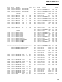
SPECIFICATIONS
Main unit
Tuner section
Amplifier section
FM stereo, FM/AM superheterodyne tuner
For the U.S.A. model
FM tuner section
Tuning range
U.S.A. model:
AUDIO POWER SPECIFICATIONS
POWER OUTPUT AND TOTAL HARMONIC
DISTORTION:
With 6-ohm loads, both channels driven, from
120 – 10,000 Hz; rated 10 watts per channel
minimum RMS power, with no more than 10%
total harmonic distortion from 250 milli watts to
rated output.
European model:
DIN power output (rated): 7.5 + 7.5 watts
(6 ohms at 1 kHz, DIN)
Continuous RMS power output (reference):
10 + 10 watts
(6 ohms at 1 kHz, 10%
THD)
Inputs
ANALOG IN (mini jack): Sensitivity 450 mV,
impedance 10 kilohms
Outputs
PHONES (mini jack):
accepts headphones with
an impedance of 8 ohms or
more
European models:
Antenna
Antenna terminals
Intermediate frequency
AM tuner section
Tuning range
U.S.A. model:
European model:
Antenna
Antenna terminals
Intermediate frequency
Speaker system
System
Laser
Frequency response
9-879-721-02
2005H05-1
© 2005.08
87.5 – 108.0 MHz
(100-kHz step)
87.5 – 108.0 MHz
(50-kHz step)
FM lead antenna
75 ohms unbalanced
10.7 MHz
530 – 1,710 kHz
(with the tuning interval
set at 10 kHz)
531 – 1,710 kHz
(with the tuning interval
set at 9 kHz)
531 – 1,602 kHz
(with the tuning interval
set at 9 kHz)
AM loop antenna
External antenna terminal
450 kHz
Speaker section
CD player section
Compact disc and digital
audio system
Semiconductor laser
(λ=770 – 810 nm)
Emission duration:
continuous
2 Hz – 20 kHz (±0.5 dB)
Sony Corporation
Audio Group
Published by Sony Engineering Corporation
Speaker units
Woofer:
Tweeter:
2-way, Acoustic
Suspension type
Nominal impedance
9 cm dia., cone type
2.5 cm dia., balanceddome-type
6 ohms
General
Power requirements
U.S.A. model:
European model:
Power consumption
U.S.A. model:
European model:
120 V AC, 60 Hz
230 V AC, 50/60 Hz
40 watts
40 watts
0.3 watts (in Power Saving
mode)
Dimensions (w/h/d) incl. projecting parts and controls
Approx. 460 × 175 ×
190 mm
Mass
Approx. 5.3 kg
Supplied accessories
Remote Commander with
battery (1)
AM loop antenna (1)
FM lead antenna (1)
Network cable (1)
M-crew Server CD-ROM
(1)
Design and specifications are subject to change
without notice.
NETWORK AUDIO SYSTEM
HCD-CZ1/NAS-CZ1
Notes on chip component replacement
• Never reuse a disconnected chip component.
• Notice that the minus side of a tantalum capacitor may be
damaged by heat.
Flexible Circuit Board Repairing
• Keep the temperature of the soldering iron around 270 ˚C
during repairing.
• Do not touch the soldering iron on the same conductor of the
circuit board (within 3 times).
• Be careful not to apply force on the conductor when soldering
or unsoldering.
CAUTION
Use of controls or adjustments or performance of procedures
other than those specified herein may result in hazardous radiation
exposure.
The following caution label is located inside the unit.
This appliance is
classified as a CLASS 1
LASER product. This
marking is located on the
bottom exterior.
SAFETY CHECK-OUT
After correcting the original service problem, perform the following
safety check before releasing the set to the customer:
Check the antenna terminals, metal trim, “metallized” knobs, screws,
and all other exposed metal parts for AC leakage.
Check leakage as described below.
LEAKAGE TEST
The AC leakage from any exposed metal part to earth ground and
from all exposed metal parts to any exposed metal part having a
return to chassis, must not exceed 0.5 mA (500 microamperes.).
Leakage current can be measured by any one of three methods.
1. A commercial leakage tester, such as the Simpson 229 or RCA
WT-540A. Follow the manufacturers’ instructions to use these
instruments.
2. A battery-operated AC milliammeter. The Data Precision 245
digital multimeter is suitable for this job.
3. Measuring the voltage drop across a resistor by means of a
VOM or battery-operated AC voltmeter. The “limit” indication
is 0.75 V, so analog meters must have an accurate low-voltage
scale. The Simpson 250 and Sanwa SH-63Trd are examples
of a passive VOM that is suitable. Nearly all battery operated
digital multimeters that have a 2 V AC range are suitable. (See
Fig. A)
To Exposed Metal
Parts on Set
0.15 µF
1.5 kΩ
AC
voltmeter
(0.75 V)
Earth Ground
Fig. A. Using an AC voltmeter to check AC leakage.
SAFETY-RELATED COMPONENT WARNING!!
COMPONENTS IDENTIFIED BY MARK 0 OR DOTTED LINE
WITH MARK 0 ON THE SCHEMATIC DIAGRAMS AND IN
THE PARTS LIST ARE CRITICAL TO SAFE OPERATION.
REPLACE THESE COMPONENTS WITH SONY PARTS WHOSE
PART NUMBERS APPEAR AS SHOWN IN THIS MANUAL OR
IN SUPPLEMENTS PUBLISHED BY SONY.
2
HCD-CZ1/NAS-CZ1
TABLE OF CONTENTS
1. SERVICE NOTE ................................................................. 4
2. GENERAL .......................................................................... 15
3. DISASSEMBLY
3-1.
3-2.
3-3.
3-4.
3-5.
3-6.
3-7.
3-8.
3-9.
Disassembly Flow ............................................................ 17
Speaker Grill (F/R) Assy, Top Panel Assy ........................ 18
Cover Bottom Assy ........................................................... 18
Rear Panel Section ............................................................ 19
Front Panel Section .......................................................... 20
Top Panel Section ............................................................. 20
Base Unit (BU-K7BD81B) .............................................. 21
MAIN Board Section ........................................................ 21
ETHER Board, MAIN Board ........................................... 22
7. EXPLODED VIEWS
7-1.
7-2.
7-3.
7-4.
7-5.
7-6.
7-7.
Speaker Grill, Top Panel Section ...................................... 54
Front Panel Section .......................................................... 55
Rear Panel Section ............................................................ 56
CD Panel Section .............................................................. 57
PSAMP Board Section ..................................................... 58
MAIN Board Section ........................................................ 59
Base Unit (BU-K7BD81B) .............................................. 60
8. ELECTRICAL PARTS LIST ......................................... 61
4. TEST MODE ...................................................................... 23
5. ELECTRICAL ADJUSTMENTS ................................. 26
6. DIAGRAMS
6-1.
6-2.
6-3.
6-4.
6-5.
6-6.
6-7.
6-8.
6-9.
6-10.
6-11.
6-12.
6-13.
6-14.
6-15.
6-16.
6-17.
Block Diagram – SERVO Section – ................................ 27
Block Diagram – Ethernet Section – ............................... 28
Block Diagram – MAIN Section – .................................. 29
Printed Wiring Board – CD Board – .............................. 31
Schematic Diagram – CD Board – .................................. 32
Printed Wiring Board – ETHER Board – ........................ 33
Schematic Diagram – ETHER Board – ........................... 34
Printed Wiring Board
– MAIN Board (Component Side) – ................................ 35
Printed Wiring Board
– MAIN Board (Conductor Side) – .................................. 36
Schematic Diagram – MAIN Board (1/2) – .................... 37
Schematic Diagram – MAIN Board (2/2) – .................... 38
Printed Wiring Boards – Power Section – ....................... 39
Schematic Diagram – Power Section – ........................... 40
Printed Wiring Boards – Panel Section – ........................ 41
Schematic Diagram – Panel Section – ............................ 42
Printed Wiring Board – FL Board – ................................ 43
Schematic Diagram – FL Board – ................................... 44
3
HCD-CZ1/NAS-CZ1
SECTION 1
SERVICING NOTES
NOTES ON HANDLING THE OPTICAL PICK-UP
BLOCK OR BASE UNIT
The laser diode in the optical pick-up block may suffer electrostatic
break-down because of the potential difference generated by the
charged electrostatic load, etc. on clothing and the human body.
During repair, pay attention to electrostatic break-down and also
use the procedure in the printed matter which is included in the
repair parts.
The flexible board is easily damaged and should be handled with
care.
: LEAD FREE MARK
Unleaded solder has the following characteristics.
• Unleaded solder melts at a temperature about 40 ˚C higher
than ordinary solder.
Ordinary soldering irons can be used but the iron tip has to be
applied to the solder joint for a slightly longer time.
Soldering irons using a temperature regulator should be set to
about 350 ˚C.
Caution: The printed pattern (copper foil) may peel away if
the heated tip is applied for too long, so be careful!
• Strong viscosity
Unleaded solder is more viscou-s (sticky, less prone to flow)
than ordinary solder so use caution not to let solder bridges
occur such as on IC pins, etc.
• Usable with ordinary solder
It is best to use only unleaded solder but unleaded solder may
also be added to ordinary solder.
LASER DIODE AND FOCUS SEARCH OPERATION
CHECK
During normal operation of the equipment, emission of the laser
diode is prohibited unless the upper lid is closed while turning ON
the S601. (push switch type)
The following checking method for the laser diode is operable.
• Method
Emission of the laser diode is visually checked.
1. Open the upper lid.
2. Push the S601 as shown in Fig.1.
Note: Do not push the detection lever strongly, or it may be bent or damaged.
3. Press the B button.
4. Check the object lens for confirming normal emission of the
laser diode. If not emitting, there is a trouble in the automatic
power control circuit or the optical pick-up.
In this operation, the object lens will move up and down 2
times along with inward motion for the focus search.
S601
Fig.1 Method to push the S601
4
NOTES ON LASER DIODE EMISSION CHECK
The laser beam on this model is concentrated so as to be focused on
the disc reflective surface by the objective lens in the optical pickup block. Therefore, when checking the laser diode emission,
observe from more than 30 cm away from the objective lens.
UNLEADED SOLDER
Boards requiring use of unleaded solder are printed with the leadfree mark (LF) indicating the solder contains no lead.
(Caution: Some printed circuit boards may not come printed with
the lead free mark due to their particular size)
MODEL IDENTIFICATION
Power voltage indication
– Bottom View –
MODEL
US model
AEP, UK models
Power Voltage Incdication
AC: 120 V 60 Hz 25 W
AC: 230 V - 50/60 Hz 25 W
HCD-CZ1/NAS-CZ1
NETWORK CHECK
1. Apparatuses And Materials Prepared
(1) Personal computer with OS “Windows XP” (must satisfy the
conditions mentioned on pages 5 and 6 of Installation
Instructions for M-crew Server ver 1.1 (refer to page 9 of this
service manual))
(2) M-crew Server CD-ROM (for install)
(3) LAN cable
- Must comply with Category 5;
- If the set is directly connected to a personal computer:
Use a cross cable;
- If the set is connected to a personal computer via router of
hub;
- Use the LAN cable attached (part No. 1-827-478-11, 5m,
straight) or LAN cable that complies with the Category 5.
3.1 Errors In The Midway Of Server Connection
3.1.1 NETWORK function does not start
If the NETWORK function does not start though the [NETWORK]
and USER PROFILE [1] to [5] buttons on the set is pressed.
(1) Faulty connection between CN651 of MAIN board and CN501
of ETHER board
t Check if the connector is inserted obliquely of
disconnected.
(2) Faulty circuits of ETHER board
t Replace the ETHER board and check the operation.
If the board is faulty, check the soldering of power line,
communication line, etc.
- CN501
- FB505, FB508-511, FB515-521
- IC506
- R530, 537
2. Network Connection Check
2.1 Installing the M-crew Server
- Install the M-crew Server from the CD-ROM.(for the
procedure, see pages 8 to 10 of the Installation Instructions
for M-crew Server ver1.1 (refer to page 9 to 10 of this service
Section manual)
- Use a sample music file created during the installation, if
listening to the music.
2.2 Connecting the set to server, and operation check
(1) Start the personal computer in which the M-crew Server was
installed.
(2) Connect the set to the Ethernet connector of personal computer
with the LAN cable.
(3) Following “Selecting a server” on pages 13 and 14 of the
Operating Instructions for NAS-CZ1 (refer to page 11 of this
service manual), connect the set to the server.
2.3 Operation check
Following the pages 15-17 of the Operating Instructions for NASCZ1 (refer to page 11 to 12 of this service manual), check that a
music file in the server can be played with the set.
If it cannot be played normally, see“3. Remedies in Case of
Problems” in the next section.
3. Remedies In Case Of Problems
If a problem occurred in “2 Network Connection Check” mentioned
above, first check the following two items:
(1) Problem and remedies (see pages 31 and 32 of the Operating
Instructions for NAS-CZ1)
(2) Messages (see page 33 of the Operating Instructions for NASCZ1 (refer to page 8 of this service manual))
If the above two items cannot cope with the problem, take the
following procedure for checking
3.1.2 NETWORK function starts but access to network failed or
server is not found
(1) “Check Network” is displayed
t Replace the ETHER board and check the operation.
If the board is faulty, the PHY IC (IC501) on the ETHER
board may be defective.
3.1.3 “Configuring” is displayed for a long time
(1) Check if the connectable serve has started.
t If the server has not started yet, start it.
(2) It will take 1 to 2 minutes for Windows to automatically get IP
address if the set is connected to a personal computer directly
and IP address acquisition method is set to “automatic”. For
this reason, “Configuring” may be displayed for a long time.
t The use of a router with DHCP, for instance, can shorten
the time.
(3) Communication with the server is disabled and “Configuring”
will be displayed for a long time, if network setting of the set
is different from that of personal computer.
t Make correct network setting.
Example:
- Set the IP address acquisition of both the set and
personal computer to “automatic”.
- If the IP address acquisition of either the set or personal
computer or both of them is set to “static”, check that
the input field of IP address where the subnet mask”255"
is set is same between the set and personal computer.
If the subnet mask is “255.255.255.0”, three input fields
from the top must be same between the set and personal
computer.
3.1.4 “No Server” is displayed
(1) If the network setting is different between the set and personal
computer, “Configuring” is displayed for a long time and then
finally “No Server” is displayed.
t See the item of 3.1.3(3).
5
HCD-CZ1/NAS-CZ1
3.2 Errors After Serve Connection
3.2.1 “Loading” is displayed for a long time
(1) When the set is connected to the M-crew Server for the first
time, the M-crew Server identifies the HCD-CZ1 individually
and creates the profile information in the personal computer,
and therefore it will take time for “Loading”
t wait for a while as it is until “loading” finishes.
(2) When the set is connected to a DLNA server other than Mcrew server, if many contents have been stored in that server,
it will take time for “loading”.
t Though “Loading” will finish after a while, it is
recommended that the music be imported with the Mcrew Server and the M-crew Server be used as a server.
3.2.2 “Server Error” is displayed
(1) If the load on personal computer is large, the communication
with the set will not finish within the specified time, resulting
in “Serve Error” Display.
t Reduce the load on personal computer, and then retry.
(2) “Server Error” will be displayed if the server information is
refreshed (addition or deletion of music) when you are listening
to the music with the set.
t Reconnect the set to the server.
3.3 Errors When You Are Listening To The Music
3.3.1 Sounds are interrupted
(1) The baud rate will be reduced in the wireless connection
t Cable connection is recommended.
(2) Check if the music itself registered to the server is interrupted.
t Certain ripping software may not be able to encode the
music-to-music joints continuously.
3.3.2 Some functions cannot be used
(1) If a server other than M-crew Server is used, the following
functions cannot be used. Following the pages 13 and 14 of
the Operating Instructions for NAS-CZ1 (refer to page 11 of
this service manual), select the M-crew Server.
- Web Radio
- Library Mode switching
- Library Search
- Favorite
- User Profile
3.3.3 “Cannot Play” is displayed
(1) If the server does not convert the music into LPCM format for
streaming, the set cannot play that music.
t You can play the contents supported by the M-crew Server,
if the set is connected to the M-crew Server.
(2) The contents with DRM may not be processed for streaming.
t The contents with DRM are not supported.
(3) “Cannot Play” will be displayed if the contents themselves
are deleted though the music contents are registered to the
server.
3.3.4 Operation becomes slow
(1) If it takes time to communicate with the server, the operation
of the set may become slow according to that time.
6
HCD-CZ1/NAS-CZ1
• Operating Instrution for NAS-CZ1 (extract)
Connecting power cord
Connect the power cord to a wall outlet.
The demonstration appears in the display. When
you press ?/1, the system turns on and the
demonstration automatically ends.
To turn off the demonstration
display
Press DISPLAY while the system is off
(page 28).
Enjoying NETWORK function
When selecting the M-crew
Server as a media server
Checking the network status
network lamp
The following marks appears in the display.
You can listen to music stored on the connected
media server with this system.
Selecting a server
The server selected now*
You can select your desired Media server to be
your default server. Doing so prevents you from
having to make the selection each time you use
NETWORK function.
4
5
Network lamp System status
Press ?/1 to turn on the system.
Press NETWORK.
Tip
Tip
While “Configuring” is flashing in the
display, the display is automatically setting.
Do not turn off the power during this time.
You can redo the default server selection to select a
different server (page 19).
When the network lamp flashes quickly, a message
also appears in the display at this time (see page 33).
To check the message again, press ENTER or another
button while [NET] appears in the display.
You can listen to music stored on DLNA-compliant
servers with this system.
2
3
Note
You can use the following functions only when using
the M-crew Server as a media server.
– MUSIC LIBRARY
– LIBRARY SEARCH
– PLAYLIST MODE
– FAVORITE PLAYLIST
– User Profile
– WEB RADIO
Tip
1
* These marks also appear when using a server other
than M-crew Server.
Start up your desired Media server on
your computer.
flashes slowly
The system is communicating with
the server.
lights up
The NETWORK function is being
used.
An error has occurred.
flashes quickly
“MEDIA SERVERS?” appears, then
press ENTER.
Press . or > repeatedly to select
the desired Media server, then press
ENTER.
The selected server is set to the default
server.
2
MUSIC LIBRARY
Press LIBRARY MODE repeatedly until
the mode you want appears.
Select
To play
Listening to music stored
on your computer
(Disc mode)
Mode for listening to
albums sorted according to
the disc information of the
tracks
You can listen to music stored on your computer
through the system’s speaker. Make sure you
have registered audio data to the media server.
(Artist mode)
Mode for listening to
albums sorted according to
the artist information of the
tracks
(Playlist mode) Mode for listening to
playlists created by M-crew
Server and the favorite
playlists registered on the
M-crew Server.
1
3
2
3
X
1
2
3
Press NETWORK repeatedly to switch
the function to MUSIC LIBRARY.
Press LIBRARY MODE repeatedly until
“
(Disc mode) ” or “ (Artist mode)”
appears.
Press LIBRARY SEARCH.
“LIBRARY SEARCH” appears about a
second, then “SEARCH” lights up.
4
Repeat the following to search for the
album.
To do
Press
Change the character
at the cursor position
(flashing character)
./> repeatedly
x
Some time may be required before playback starts
depending on the number of tracks registered to the
server.
./>
Other operations
m/M
To
Do this
Move the cursor
position
CURSORT or
CURSORt
repeatedly
Stop play
Press x.
Press X. Press again to resume
play.
Display albums with
titles that match the
characters from the
start to the cursor
position
ALBUM +/– repeatedly
Pause
REPEAT
Press NETWORK repeatedly to switch
the function to MUSIC LIBRARY.
Select an album Press ALBUM +/– repeatedly.
Select a track
Press . or > repeatedly.
Find a point in a Keep pressing m or M during
track
playback and release it at the
desired point.
(Disc mode)
You can search for an album in either DISC
MODE or ARTIST MODE.
Note
ALBUM +/–
1/ALL
1
Press N.
Searching for an album
– L IBRARY SEARCH
Play repeatedly
(Repeat Play)
(Artist mode)
(Playlist mode)
Play all tracks
only in the
selected album
Press REPEAT repeatedly during
playback until “REP” or “REP1”
appears.
REP: For all registered tracks.
REP1: For a single track only.
To cancel Repeat Play, press
REPEAT repeatedly until both
“REP” and “REP1” disappear.
5
Listening to music in a
play list
– P LAYLIST
You can listen to tracks registered in the
PLAYLIST album on your computer.
1
2
3
4
Press NETWORK repeatedly to switch
the function to MUSIC LIBRARY.
Press LIBRARY MODE repeatedly until
“ (Playlist mode)” appears.
Press ALBUM +/– repeatedly to select a
desired playlist.
Press N.
Note
Some time you may not be able to use the Playlist
library function with a media server other than the
supplied M-crew Server.
Press ENTER or N.
Playback starts from the first track in the
selected album.
Notes
Y ou cannot use the Library Search function with a
media server other than the supplied M-crew Server.
Y ou cannot search for an album in PLAYLIST
MODE.
Press 1/ALL repeatedly until
“1ALBM” appears.
To play all registered tracks, press
1/ALL repeatedly until “ALL
ALBM” appears.
Note
The X and m/M buttons may not work for some
tracks when using a server other than M-crew Server.
7
HCD-CZ1/NAS-CZ1
Listening to music in a
favorite list
1
2
What is a FAVORITE PLAYLIST?
Tip
FAVORITE
CALL
FAVORITE
DELETE
ENTER
To register tracks to a favorite
playlist and playing
1
During the playback or play pause of the
desired track, press FAVORITE ADD.
“FAVORITE” appears.
2
After “FAVORITE” disappears, repeat step 1
to register the desired tracks.
Problems and remedies
Press FAVORITE CALL.
Play starts.
You can also play the favorite playlist through the
following procedure:
1. Press LIBRARY MODE repeatedly until “
(Playlist mode)” appears.
2. Press ALBUM +/– repeatedly until “FAVORITE”
appears.
To delete tracks from a favorite
list
1
Troubleshooting
Press NETWORK repeatedly to switch
the function to MUSIC LIBRARY.
– FAVORITE PLAYLIST Registration/
FAVORITE PLAYLIST Play
By registering tracks on your computer to a
favorite list using this system, you can play back
only the tracks you want to listen to. One
favorite playlist can be created for each profile,
and each favorite playlist can contain up to 100
tracks.
Network
Playing favorite playlist
1
Press N or X to play or pause the track you
want to delete from a favorite playlist.
2
Press FAVORITE DELETE.
“DELETE?” appears.
3
Press ENTER.
“Deleting” appears, then “Complete!”
appears.
Notes
• If you edit a track in an album that is registered to a
FAVORITE PLAYLIST on your computer, the track
is erased from the FAVORITE PLAYLIST
automatically. (except when you changed the track
name)
• During the playback of a track in a favorite playlist,
you cannot press FAVORITE ADD to register the
track to a favorite playlist.
• When you press FAVORITE DELETE, the track is
erased from the FAVORITE PLAYLIST but remains
in the Music Library.
Should you encounter a problem with your
system, do the following:
1
Make sure the power cord is correctly and
firmly connected.
2
Find your problem in the troubleshooting
checklist below and take the indicated
corrective action.
If the problem persists after doing all of the
above, consult your nearest Sony dealer.
General
The display starts flashing as soon as you
plug in the power cord even though you have
not turned on the system (see step 2 of
“Connecting power cord” (page 13)).
Press ?/1 while the system is off. The
demonstration disappears.
The radio presetting is canceled.
Redo “Presetting radio stations” (page 24).
There is no sound.
Press VOL + or VOLUME + on the system.
Make sure the headphones are not connected.
There is severe hum or noise.
Move the system away from the source of noise.
Connect the system to a different wall outlet.
I nstall a noise filter (commercially available) to
the power cord.
The remote does not function.
Remove the obstacle.
M ove the remote closer to the system.
P oint the remote at the system’s sensor.
Replace the CR2025 battery.
L ocate the system away from the fluorescent light.
The system can not be turned on even though
you have pressed ?/1.
Make sure the power cord is connected to a wall
outlet.
The desired server cannot be found.
• Check the network settings on your computer.
• Start up the server you want to use on your
computer.
• Check the network settings.
• Set the broadband router or hub again correctly.
For details, see the instruction manual of the
broadband router or hub.
• When setting a firewall other than that provided
with the OS, refer to Troubleshooting in the
Installation Manual included on the supplied
CD-ROM.
• Reduce the number of servers that can be
connected to 10 servers or less (page 21).
• Replace the Ethernet cable with a new one.
• Follow the procedure below and reconnect to the
server.
1. Select “MEDIA SERVERS?” in the network
menu (page 19), then press ENTER.
2. Press ./> repeatedly to select the
desired media server, then press ENTER.
Tracks registered to a server cannot be
selected by the system.
• Track selection, playback and other operations on
the system side may not be possible for servers
other than M-crew Server (page 13).
The sound skips.
S ound skipping may occur in the following cases:
– When music is being recorded onto the server
– When the computer is running many
applications
– When the network status is crowded
– When multiple systems are performing
playback simultaneously
Track names are not displayed.
• Some types of input characters cannot be
displayed by the system, even if they can be
registered and displayed on the server.
Operation commands take time.
• Depending on the condition of the server, it may
take a while until operation proceeds. For
example, when there is no response after pressing
m/M, keep pressing m/M for a while.
Afterwards, operation sould begin.
The color irregularity on a TV screen appears.
T urn off the TV set once, then turn it on after 15
to 30 minutes. If the color irregularity still
persists, place the speakers farther away from the
TV set.
CD/MP3 player
• Find a place and an orientation that provide good
reception, then set up the antenna again. If you
cannot obtain good reception, we recommend you
connect a commercially available external
antenna.
• The supplied FM lead antenna receives signals
along its entire length, so make sure you extend it
fully.
• Locate the antennas as far away from the speaker
cords as possible.
• Consult your nearest Sony dealer if the supplied
AM antenna has come off the plastic stand.
• Try turning off surrounding electrical equipment.
Abnormal noise is produced.
• Check whether a disc that the system cannot play
is loaded.
Play does not start.
• Check whether a disc is loaded. The disc indicator
lights when a disc is loaded.
• Wipe the disc clean (page 34).
• Replace the disc.
• Place a disc that this system can play.
• Place the disc correctly.
• Remove the disc and wipe away the moisture on
the disc, then leave the system turned on for a few
hours until the moisture evaporates.
• Press N to start play.
The sound skips.
• Wipe the disc clean (page 34).
• Replace the disc.
• Try moving the system to a place without
vibration (e.g., on top of a stable stand).
MP3 audio track cannot be played back.
• Recording was not performed according to the
ISO9660 level 1 or level 2 format, or Joliet in the
expansion format.
• The MP3 audio track does not have the extension
“.MP3”.
• The data is not stored in MP3 format.
• Discs containing files other than MPEG1, 2, 2.5
Audio Layer-3 files cannot be played.
MP3 audio tracks take longer to play back than
others.
• After the system reads all tracks on the discs,
playback may take more time than usual if:
– the number of albums or tracks on the disc is
very large.
– the album and track organization structure is
very complex.
The album title, track title and ID3 tag do not
appear correctly.
• Use a disc that conforms with ISO9660 level 1,
level 2, or Joliet in the expansion format.
• The disc ID3 tag is not ver. 1 or ver. 2.
A stereo FM program cannot be received in
stereo.
• Press FM MODE until “MONO” disappears.
Optional components
There is no sound.
• Refer to General items “There is no sound.” and
check the condition of the system.
• Connect the component properly (page 30) while
checking:
– if the cords are connected properly.
– if the cord plugs are firmly inserted all the way.
• Turn on the connected component.
• Refer to the operating instructions supplied with
the connected component and start playing.
• Press FUNCTION repeatedly to select
“ANALOG IN” (page 30).
The sound is distorted.
• Set the volume of the connected component
lower.
If the system still does not
operate properly after performing
the above measures, reset the
system as follows:
Tuner
1
2
3
4
Severe hum or noise.
Stations cannot be received.
• Set the proper band and frequency (page 24).
• Connect the antenna properly (page 11).
The system is reset to the factory settings. You
should set the settings you made, such as the
preset stations.
8
Disconnect the power cord.
Reconnect the power cord.
Press ?/1 to turn on the system.
Press x, USER PROFILE 5 and POWER,
on the system at the same time.
Messages
If a message appears while using the system,
follow the procedures below to correct the
problem.
Network
Cannot Play
• The track cannot be played in the following cases:
– Sampling Rate is other than 32 kHz, 44.1 kHz,
48 kHz.
– The track is not being streamed by linear PCM.
– The track is other than one channel or two
channel.
– The track sampling bits are other than 16 bits.
– The server status is busy.
Check Network
• Check t hat the Ethernet cable between the system
and the hub or router is firmly connected.
• Check that the hub or router is turned on.
IP Conflict
• Set the IP addresses of the system and other
devices on the network so that there is no
duplication (page 20).
No album
• Register the track as instructed by the operation
manual of the connected server.
• Follow the procedure below and reconnect to the
server.
1. Select “MEDIA SERVERS?” in the network
menu (page 19), then press ENTER.
2. Press ./> repeatedly to select the
desired media server, then press ENTER.
No Server
• Start up the server. M-crew Server can be started
up by the following method:
Right-click the task tray icon, then click “Start
Music Service” in the menu.
• M-crew Server may not be recognizing the
system. Follow the procedure below and check
whether M-crew Server is recognizing the system:
1. Click [Start] – [All Programs] – [M-crew
Server] – [TOOLS] – [EQUIPMENT LIST] in
that order.
2. If the server name is not present in the list that
appears in step 1, device registration must be
performed. For details, see the Help or Install
Manual within M-crew Server.
• When setting a firewall other than that provided
with the OS, refer to Troubleshooting in the
Installation Manual included on the supplied
CD-ROM.
• Perform the TCP/IP settings correctly for the
system and the computer (page 20).
Select Server
• Follow the procedure below and reconnect to the
server.
1. Select “MEDIA SERVERS?” in the network
menu (page 19), then press ENTER.
2. Press ./> repeatedly to select the
desired media server, then press ENTER.
Server Error
• Follow the procedure below and reconnect to the
server.
1. Select “MEDIA SERVERS?” in the network
menu (page 19), then press ENTER.
2. Press ./> repeatedly to select the
desired media server, then press ENTER.
Server Close
• Start up the server. M-crew Server can be started
up by the following method:
Right-click the task tray icon, then click “Start
Music Service” in the menu.
• When you want to change the computer’s network
settings, restart the server on this system. This
message disappears after a short time.
WebRadio Error
• Register a station that can be played back on Mcrew Server.
• Connection may be difficult depending on the
internet line status. Wait a bit and then perform the
operation again.
CD/MP3
No Disc
• There is no disc in the player.
HCD-CZ1/NAS-CZ1
• Installation Instrution for M-crew Server ver1.1 (extract)
System Requirements
The following software and hardware are required in order to be able
to run M-crew Server.
s A PC/AT compatible that satisfies the
performance requirements described below.
M-crew Server does not run in an Apple Macintosh environment.
– CPU*: Intel Pentium III 600 MHz (1 GHz or more is
recommended) or Celeron 600 MHz (1 GHz or more is
recommended) or better
– RAM: 256 MB or more is recommended
– Video board and display driver: Must be capable of XGA (1024
× 768 pixels) display with at least 65,536 colors.
– Free hard disk space required for installation: At least 20 MB
(includes M-crew Server and the help, etc.)
– CD-ROM or DVD drive (for software installation and CD
recording)
– Available LAN jack: At least one
– Sound board
s Used Language: English/German/French
* Operation is guaranteed only with Intel Pentium and Celeron CPUs.
Notes
• Operations are not guaranteed for all the recommended computer environments
mentioned above.
• Operation is not assured in personally constructed PCs or operating systems and
an environment upgraded to the other operating systems.
• Original brand and home_made personal computers do not apply.
s OS: Windows XP Home Edition/Windows XP
Professional/Windows XP Media Center Edition
2004/Windows XP Media Center Edition 2005
M-crew Server does not run in a Microsoft Windows 3.1, Windows
95, Windows 98, Windows ME, Windows NT or Windows 2000
Professional environment.
When installing, log on as the administrator.
s Internet access (for Gracenote access and WEB
RADIO)
s Display: XGA (1024 × 768 pixels)
Must be able to display at least 65,536 colors.
Before installing the software
Do not connect the system to your computer before
the installation is completed!
Close down all applications running on the computer
before installing the software!
Installing
Installing M-crew Server
1
Turn on your computer and allow Windows to load.
2
Insert the supplied CD-ROM into the CD-ROM drive of
your computer.
Be sure to log on through a user name which
belongs to the computer's administrator to install the
software.
The “M-crew Server SETUP” dialog box appears.
Note
If the dialog box does not open,
double-click CD-ROM
(Setup.exe) icon.
3
Select the language to be used.
4
Click [M-crew Server setup].
The installation starts.
Note
If “.Net Framework” is not installed on your computer, “.NET Framework
Installer” dialog box appears. Click [Install] to install “.Net Framework 1.1”
and follow the displayed instructions.
5
Follow the on-screen messages.
9
HCD-CZ1/NAS-CZ1
6
After the installation is completed, click [Reboot] to restart
your computer.
Be sure to restart your computer only after the installation has
been completed.
After restarting your computer, the “AUTO LINK FOLDER
SETUP” window appears.
For Windows XP SP2
The “Windows Security Alert” dialog box appears.
Click [Unblock] to unblock the program.
Check that [Name] is “M-crew Server task tray icon”, then click
the [Unblock] button. If you click the [Keep Blocking] button,
you will be unable to use M-crew Server (page 20).
9
Turn on the system. The system is registered automatically
on your computer. To register the system on your computer
manually, see “Registering the system on your computer
manually” on page 14.
Notes
• When SP2 has not been applied to Windows XP, M-crew Server may not operate
properly unless the latest Windows Security Update is applied. In these cases,
apply the latest Windows Update (KB885835) or check the contents noted at the
following website and take the necessary measures.
http://www.sony.net/Products/OpenMG/support/840987/
• The M-crew Server software uses the installed folders, so do not delete, move, or
edit any of the installed folders. Managing these folders like general files on
Windows Explorer could cause the contents to become unstable or corrupted.
• While the installation is still in progress, do not interrupt the operation or take the
CD-ROM out of the CD-ROM drive. Doing so may render it impossible to install
the software thereafter.
Tip
The following modules are installed.
Microsoft Module1) .Net Framework Version1.1
Microsoft Data Access Components (MDAC) 2.8 (as
necessary)
Windows MediaFormatSDK9 Runtime
7
OpenMG SDK
Click [NEXT].
The contents located on the path set to ON by the checkbox are
loaded automatically. When not making this setting, click the
[Skip] button.
The connection manual appears automatically.
For Windows XP SP2
See “Making the ICF Settings” on page 12 when the “ICF
Setting” dialog opens.
OpenMG SDK 3.4.01
OpenMG Limited Patch
Other related modules
CDDB22)
CDDB2 Module
Music Server
Mcrew Music Server
Other related modules
M-crew Server
M-crew Server
Other related modules
1) Refer
to the Microsoft home page and other materials for a detailed description
of these Microsoft Modules.
to www.gracenote.com for a detailed description of CDDB2.
2) Refer
8
Confirm the optimum connection method, and connect the
system to your computer.
Other Information
Starting up M-crew Server
Click [Start] – [All Programs] – [M-crew Server] – [M-crew
Server] in that order.
Or, double-click the M-crew Server icon on the taskbar.
Or, right-click the M-crew Server icon on the taskbar, and
select “M-crew Server”.
Making the ICF Settings
When the M-crew Server icon in the taskbar appears as
ICF (Internet Connection Firewall) settings.
1
, make the
Click [Start] – [All Programs] – [M-crew Server] –
[TOOLS] – [ICF Settings] in that order.
“ICF SETTINGS” window appears.
2
Click the port with NG status.
A dropdown menu with port numbers appears.
If “OK” appears for all server status items, there is no need to
make the ICF settings. Click [Close] to close the window.
3
Select any different port number.
4
Click [Apply].
“OK” or “NG” appears.
10
5
Repeat steps 2 to 4 until “OK” appears for all status items.
6
Click [Close].
HCD-CZ1/NAS-CZ1
Tips
• Windows XP and later versions have a simple firewall function as a standard
feature. This firewall function is called “ICF”, and lets users limit
communications between home networks or small-scale office networks and the
internet. When this firewall is enabled, the firewall must be set to allow
communication of specific ports and programs in order to perform
communication between M-crew Server and this system. These settings are made
at the ICF SETTINGS window. However, note that making these settings may
expose your computer to illicit access.
• When communication is limited by firewall software other than the OS
functions, enable the following .exe files. For a detailed description of the setting
method, see the operation manual of the firewall software used.
– McrewServer.exe
– McTaskTray.exe
– McService.exe
– McFolderWatcher.exe
– McrewHttpService.exe
– McrewUPnPService.exe
Registering the system on your computer
manually
When the system is connected to your computer after installing the Mcrew Server, the system is registered automatically on your computer.
Register the system on your computer manually for higher security.
1
Turn on the system.
2
Press NETWORK on the remote repeatedly to switch the
function to MUSIC LIBRARY or WEB RADIO.
3
Press NETWORK MENU on the remote.
4
Press . or > on the remote repeatedly until
“REGISTRATION?” appears, then press ENTER on the
remote.
The count down display appears in the display of the system.
5
Click [Start] – [All Programs] – [M-crew Server] –
[TOOLS] – [EQUIPMENT LIST] in that order.
“M-crew Server EQUIPMENT LIST” dialog box appears on
your computer screen.
For Windows XP SP2
The “Windows Security Alert” dialog box appears.
Check that [Name] is “MCMachineRegist.exe”, then click the
[Unblock] button. If you click the [Keep Blocking] button, you
will be unable to use M-crew Server (page 20).
Uninstalling the M-crew Server software
Log on through a user name which belongs to the computer’s
administrator and follow the procedures below.
Refer to the operating instructions of your computer for details on
logging on as a user name which belongs to the computer’s
administrator.
1
Stop the service from the task tray icon.
Right-click the task tray icon, then click [Stop Music
Service] in the menu.
The task tray icon display becomes dim.
2
Hide the task tray icon.
Right-click the task tray icon, then click [Hide task tray
icon] in the menu.
The task tray icon display disappears.
6
3
When Windows XP is in Classic View, switch to Category
View, then click [Start] – [Control Panel] – [Add or
Remove Programs] in that order.
4
Select [M-crew Server], and click [Change/Remove].
5
Select [Mcrew Music Server], and click [Change/Remove].
6
Reboot the computer.
Set “Equipment selection mode:” to “Manual”, and click
[Add] on your computer.
The registration starts.
“Complete!” appears in the display of the system when the
registration is complete.
11
HCD-CZ1/NAS-CZ1
Notes
• When uninstalling M-crew Server, a command prompt window appears.
Command prompt processing may take some time. However, the uninstall work
is proceeding during this time, so do not click the [Cancel] button in the
“Installsheild” dialog.
• “OpenMG Limited Patch ***” and “OpenMG Secure Module ***” may be used
by other software (SonicStage, VAIO Media, etc.). If Open MG SDK is not
being used, uninstall “OpenMG Limited Patch ***” and “OpenMG Secure
Module ***” in the “Add or Remove Programs” window.
Troubleshooting
Should you encounter a problem while installing or uninstalling Mcrew Server, use the following troubleshooting to remedy the problem.
If the problem persists after checking all the below items, fill in the
following table and then consult your nearest Sony dealer.
In case an error message appears, it is recommended that you write it
down.
Computer
• Manufacturer:
• Model:
• Type: Desktop type / Laptop type
Name of operating system:
RAM:
Hard disk drive (containing M-crew Server and audio data)
• Capacity of the drive:
• Free space:
Installed folder containing M-crew Server (if other than the default folder)1)
• Location of the installed folder:
Version of the software (M-crew Server Ver.1.0)2):
Error Message (if one appeared):
If an externally connected CD-ROM drive is used
• Manufacturer:
• Model:
• Type: CD-ROM / CD-R/RW / DVD-ROM / Other (
• Type of connection to the computer: PC card / USB / IEEE1394 / Other
(
)
)
If another device with USB connection is used
• Name of the device (or devices):
1)
2)
M-crew Server does not start up
• Server ports do not open.
1 Click [Start] – [All Programs] – [M-crew Server] – [TOOLS] –
[ICF Settings] in that order.
“ICF SETTINGS” window appears.
2 Click the port with NG status.
A dropdown menu with port numbers appears.
3 Select any different port number.
4 Click [Apply].
“OK” or “NG” appears.
5 Repeat steps 2 to 4 until “OK” appears for all status items.
If you do not specify the destination, the software is installed at C:\Program
Files\Mcrewserver.
To check the M-crew Server software version, right-click in the M-crew Server
window and select “About M-crew Server”, or see the version information on the
supplied CD-ROM.
Installation was not successful
• Be sure to close down all applications before installing
the software.
If you start the installation while other programs are running, a
malfunction may occur. This is especially true for programs that
require large amounts of system resources, such as virus-check
software.
• Make sure your computer has enough hard disk drive
space.
150 MB of free space or more on the hard disk drive is required. If
your computer does not have enough space, the installation may
not be possible.
• The [Keep Blocking] button was clicked at the
“Windows Security Alert” dialog box when using
Windows XP SP2.
6 Click [Close].
1 Click [Start] – [Control Panel] in that order.
“Control Panel” window appears.
2 When Windows XP is in Category view, switch to Classic view,
then click [Network Connections].
3 Click “Change Window Firewall Settings” on the left edge.
“Windows Firewall” dialog appears.
4 Click the [Exceptions] tab.
5 Click [Add Program].
“Add a program” dialog appears.
12
HCD-CZ1/NAS-CZ1
6 Select “M-crew Server task tray icon” from the “Programs” list,
then click the [OK] button.
Make sure that the M-crew Server task tray icon appears and is
checked in the “Program and service” list in the “Exceptions”
tab of the “Windows Firewall” dialog.
7 Click [OK].
• If the installation is still unsuccessful after all that you
have done.
1 Click [Start] – [Control Panel] in that order.
“Control Panel” window appears.
2 When Windows XP is in Classic View, switch to Category View,
then click [Add or Remove Programs].
“Add or Remove Programs” window appears.
3 Select and click “M-crew Server” in the “Currently Installed
Programs” list.
When “M-crew Server” does not appear in the “Currently
Installed Programs” list, click [Change/Remove] and proceed to
step 6.
• The progress bar on the display is not moving. The
access lamp has not lit for a few minutes.
The installation is progressing normally. Please wait.
“No Server” appears on the NAS-CZ1.
• M-crew Server may not be recognizing the system.
When communication is limited by firewall software other than
the OS functions, enable the following .exe files. For a detailed
description of the setting method, see the operation manual of the
firewall software used.
– McrewServer.exe
– McTaskTray.exe
– McService.exe
– McFolderWatcher.exe
– McrewHttpService.exe
– McrewUPnPService.exe
4 Click [Change/Remove].
5 Follow the on-screen messages and restart your computer.
6 When the computer restarts, installation again. (See “Installing
M-crew Server” on page 8.)
• If the installation seems to be stopped
The installation may take 10 minutes or more depending on your
computer or CD-ROM drive. During the installation, watch out for
the occurrence of any of the following problems.
There is no sound from the system
Task tray icon not present
• This M-crew Server is not selected by the server
selection on the system side.
For details, refer to the operating instructions provided with the system.
• Follow the procedure below to display the icon again.
Click [Start] – [All Programs] – [M-crew Server] –
[TOOLS] – [M-crew Server task tray icon] in that order.
• The server side system registration is not correct.
• Uninstall M-crew Server and re-install it.
1 Check the connection between the system and your computer.
To check the optimum connection method, click [Start] – [All
Programs] – [M-crew Server] – [MANUAL] – [Connection
Manual] in that order.
Task tray icon darkened
The service is not active. Troubleshoot it by checking the following
items.
2 Turn on the system.
The system is registered automatically on your computer.
• Right-click the task tray icon. Click [Start Music
Service].
The server side must also be set when performing system
registration manually. See “Registering the system on your
computer manually” on page 14.
• Click [Start] – [All Programs] – [M-crew Server] –
[TOOLS] – [ICF Settings] in that order and check the
port.
• Make sure the system is properly connected. (Refer to
the connection manual. Also check your computer's
network settings.)
• Check for the M-crew Server task tray icon.
Refer to the startup instructions. Also refer to “Task tray icon not
present” on page 24.
• Make sure the M-crew Server task tray icon is lighting.
Refer to the update instructions. Also refer to “Task tray icon
darkened” on page 24.
• Make sure the system is registered in M-crew Server.
Refer to the instructions for confirming registration.
• Restart your computer.
• Cannot listen to Web Radio
Make sure that the computer’s internet access is correct.
If using a proxy server, make sure that the proxy server is set
correctly in the “PROXY SETTING” dialog box.
• Uninstall M-crew Server and re-install it.
Cannot uninstall M-crew Server
1 Stop the service from the task tray icon.
Right-click the task tray icon, then click “Stop Music Service”
in the menu.
2 Hide the task tray icon.
Right-click the task tray icon, then click [Hide Task Tray icon]
in the menu.
3 When Windows XP is in Classic View, switch to Category View,
then click [Start] – [Control Panel] – [Add or Remove
Programs] in that order.
Select the desired program and remove it.
13
HCD-CZ1/NAS-CZ1
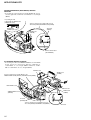
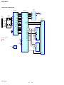
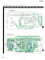
CD MECHANISM DECK (BU-K7BD81B) SERVICE
POSITION
• In checking the CD mechanism deck (BU-K7BD81B), prepare
extension jig (Part No. J-2501-248-A: 1mm Pitch, 27 cores, Length
300mm).
If operating the CD,
solder-bridge the MAIN board
(CN603 1pin, 2pin).
Connect extension jig (J-2501-248-A) to the
CD board (CN201) and MAIN board (CN700).
CD board
(CN201)
MAIN board
(CN603 1pin, 2pin)
MAIN board
(CN700)
CD mechanism deck
(BU-K7BD81B)
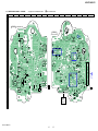
ALL BOARDS SERVICE POSITION
• In checking the FL board FRONT PANEL board and MAIN
boards, prepare two extension jigs (Part No. J-2501-077-A:
1.25mm Pitch, 13 cores, Length 300mm and Part No. J-2501009-A: 1.25mm Pitch, 15 cores, Length 300mm).
PSAMP board
MAIN board
(CN602)
Connect extension jig (J-2501-009-A) to the
FRONT PANEL board (CN1201) and MAIN board (CN601).
TOP PANEL board
SUBPS board
FRONT PANEL board
(CN1201)
ETHER board
MAIN board
(CN601)
FL board
(CN1001)
Connect extension jig (J-2501-077-A) to the
FL board (CN1001) and MAIN board (CN602).
14
CD board
HCD-CZ1/NAS-CZ1
SECTION 2
GENERAL
This section is extracted from
instruction manual.
• Location of controlls
Main unit
BUTTON DESCRIPTIONS
ALPHABETICAL ORDER
A–O
P–Z
Display window 9
FUNCTION 2
NETWORK 5
NETWORK lamp 5
PHONES jack q;
Remote sensor 8
USER PROFILE 1 – 5 3
VOL +/– 7
?/1 (On/Standby) 1
Z PUSH OPEN 4
N (play) 6
x (stop) 6
4
5
3
6
2
7
1
q;
9
8
15
HCD-CZ1/NAS-CZ1
Remote control
BUTTON DESCRIPTIONS
ALPHABETICAL ORDER
A–M
N–Z
ALBUM +/– 9
DISPLAY 2
DSGX qf
ENTER 8
FAVORITE
ADD q;
CALL q;
DELETE q;
FM MODE qj
FUNCTION wd
LIBRARY
MODE wa
SEARCH wa
NETWORK qa
MENU 7
PRESET EQ 3
REPEAT qj
SCROLL qd
SLEEP qs
TUNER BAND qg
TUNER MEMORY 5
TUNING MODE qh
TUNING +/– ql
USER PROFILE ws
VOL +/– 4
?/1 (On/Standby) 1
1/ALL 6
m/M (rewind/fast forward)
qk
TCURSOR/CURSORt qk
./> (go back/go forward)*
ql
N (play)* w;
X (pause) w;
x (stop) w;
* The N and . buttons have
tactile dots. Use the tactile dots
as a reference when operating
the system.
wd
qa
ws
1
qs
2
qd
0
wa
3
qf
9
w;
ql
16
4
6
5
qg
qk
qj
8
7
qh
HCD-CZ1/NAS-CZ1
SECTION 3
DISASSEMBLY
• This set can be disassembled in the order shown below.
3-1. DISASSEMBLY FLOW
SET
3-2. SPEAKER GRILL (F/R) ASSY,
TOP PANEL ASSY
(Page 18)
3-3. COVER BOTTOM ASSY
(Page 18)
3-4. REAR PANEL SECTION
(Page 19)
3-5. FRONT PANEL SECTION
(Page 20)
3-6. TOP PANEL SECTION
(Page 20)
3-7. BASE UNIT (BU-K7BD81B)
(Page 21)
3-8. MAIN BOARD SECTION
(Page 21)
3-9. ETHER BOARD, MAIN BOARD
(Page 22)
17
HCD-CZ1/NAS-CZ1
Note: Follow the disassembly procedure in the numerical order given.
3-2. SPEAKER GRILL (F/R) ASSY, TOP PANEL ASSY
6 top panel assy
4 speaker grill-R assy
5 three screws
(BVTP 3 × 8)
3 six bosses
3 six bosses
5 three screws
(BVTP 3 × 8)
5 three screws
(BVTP 3 × 8)
1 six bosses
1 six bosses
5 three screws
(BVTP 3 × 8)
2 speaker grill-F assy
3-3. COVER BOTTOM ASSY
2 cover bottom assy
1 five screws
(BVTP 3 × 6)
1 four screws
(BVTP 3 × 6)
18
HCD-CZ1/NAS-CZ1
3-4. REAR PANEL SECTION
1 five screws
(BVTP 3 × 16)
5 two speaker terminals (SP101)
6 rear panel section
2 four screws
(BVTP 3 × 8)
4 acoustic absorbent
cushion
1 five screws
(BVTP 3 × 16)
3
5 two speaker terminals (SP201)
4 acoustic absorbent
cushion
Note: Be sure to replace the Cushion (Part No. 2-586-851-01)
when the Rear Panel section was removed from the
Front Panel section.
front panel section
NOTE WHEN ASSEMBLING THE REAR PANEL
FRONT PANEL REAR VIEW
speaker lead wires
speaker lead wires
Note: Assemble the Rear Panel, taking care whether the
Speaker lead wires are pinched in the panel and the screws.
slot
front panel
rear panel
speaker lead wires
Note: Arrange the wires by putting the
Speaker lead wires in the slot
of the Front Panel.
front panel
19
HCD-CZ1/NAS-CZ1
3-5. FRONT PANEL SECTION
5 three speaker terminals
(SP102, SP103)
4 FFC 15P
(CN601)
2
3 FFC 13P
(CN602)
1 four screws
(BVTP 3 × 8)
5 three speaker terminals
(SP202, SP203)
6 front panel section
3-6. TOP PANEL SECTION
7 top panel section
NOTE WHEN REMOVING THE TOP PANEL
3 two screws
(BVTP 2.6)
3 two screws
(BVTP 2.6)
2 connector
(S601)
4 springFL-L
5
6 spring-F
20
1 FFC 27P
(CN201)
4 springFL-R
HCD-CZ1/NAS-CZ1
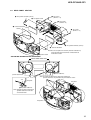
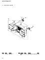
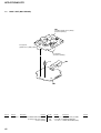
3-7. BASE UNIT (BU-K7BD81B)
7 four claws
8 CD cover
6
3 two screws
(PTPWH M2.6 × 6)
5 two vibration proof rubbers (red)
9 base unit
(BU-K7BD81B)
2 difuser
3 two screws
(PTPWH M2.6 × 6)
4 two vibration proof rubbers (green)
1 three screws
(BVTP 2.6)
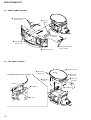
3-8. MAIN BOARD SECTION
qs two screws
(BTTP M2.6)
qj MAIN board section
qh screw
(BVTP 3 × 6)
qd bracket IC
6 FFC 15P
(CN650)
qa connector
(CN600)
2
3 connector
(CN5)
5 SUBPS board
qh screw
(BVTP 3 × 6)
4 connector
(CN603)
q; tuner pack
(TM-10CE: AEP, UK models)
(TM-10U: US model)
qh two screws
(BVTP 3 × 6)
7 two screws
(BVTP 3 × 6)
9 FFC 9P (US model)
FFC11P (AEP, UK models)
qf four screws
(BVTP 3 × 8)
8
1 four screws
(BVTP 3 × 6)
qg two screws
(BVTP 3 × 10)
21
HCD-CZ1/NAS-CZ1
3-9. ETHER BOARD, MAIN BOARD
1 two screws
(BVTP 3 × 6)
5 MAIN board
4 two screws
(BVTP 3 × 6)
3 ETHER board
22
4 two screws
(BVTP 3 × 6)
2 connector
(CN501)
HCD-CZ1/NAS-CZ1
SECTION 4
TEST MODE
FORCED RESET
* The cold reset clears all data including preset data stored in
the RAM to initial conditions. Execute this mode when
returning the set to the customer.
Procedure:
1. Press the I/1 button to turn the power on.
2. Press three buttons of I/1 , x and [5] simultaneously.
3. The message “COLD RESET” is displayed on the fluorescent
indicator tube momentarily after “See you!” is displayed, then
becomes standby states.
AMP TEST MODE
Procedure:
1. Press the I/1 button to turn the power on
2. Press three buttons of VOL – , N and [2] simultaneously.
3. In this mode, change the display as “MIN” y “21” y
“MAX” by pressing the VOL – / VOL + buttons.
4. To release this mode, press the I/1 button to execute the cold
reset and becomes standby status.
DISPLAY CHECK MODE
This mode is used to check the fluorescent indicator tube and LEDs.
Procedure:
1. Press the I/1 button to turn the power on.
2. Press three buttons of VOL – , N and [3] simultaneously.
3. When this mode is activated, the fluorescent indicator tube
and LEDs are all turned on.
4. In this mode, change the display as follows by pressing the
[NETWORK] button.
All on t FL all off t FL pattern 1 t FL pattern 2 t LED
all off t [1] LED on t [2] LED on t [3] LED on t [4]
LED on t [5] LED on t I/1 LED on t [NETWORK]
LED on t All on t...
5. To release this mode. press the I/1 button to execute the cold
reset and becomes standby status.
KEY CHECK MODE
Procedure:
1. Press the I/1 button to turn the power on.
2. Press three buttons of VOL – , N and [4] simultaneously.
3. If this mode is activated, “KEY-00/12” is displayed on the
fluorescent indicator tube.
4. In this mode, each time any key is pressed, it increment the
number of display until “KEY-12/12”
5. To release this mode, press three buttons of VOL – , N and
[4] simultaneously again.
VERSION CHECK MODE
* This mode is used to check the version of model, destination
and software.
Procedure:
1. Press the I/1 button to turn the power on.
2. Press three buttons of VOL + , [NETWORK] and [1]
simultaneously.
3. when this mode is activated, model and destination is displayed
on the fluorescent indicator tube.
4. In this mode, change the version display as model/destination
t CD-STR t Ethernet system t model/destination t ...
5. To release this mode, press the I/1 button to execute the cold
reset and becomes standby status.
CD ERROR HISTORY DISPLAY MODE
* This mode can be used for error code display of CD section.
Procedure:
1. Press the I/1 button to turn the power on.
2. Press the [FUNCTION] button to select “CD”.
3. Press three buttons of VOL + , N and [3] simultaneously.
4. When this mode is activated, it displays as follows.
Error count display:
Em 0Ed##
Em0 : Not used
Ed## : Error count of BD section
5. In this mode, change the display as error count y “MO”
display (not used) y error detail by pressing the [ALBUM -]/
[ALBUM +] keys on remote commander (RM-ANP002).
6. In the error detail display mode, change the error number and
that error detail by pressing the . or > keys on remote
commander (RM-ANP002).
Error detail display:
0***********
* : Hexadecimal number (refer to following table for detail)
7. To release this mode, press the I/1 button to turn the power
off or press the [FUNCTION] button to change the function.
CHANGE-OVER THE AM TUNING INTERVAL
(EXCEPT AEP, UK models)
The AM tuning interval can be changed over 9kHz or 10kHz
Procedure:
1. Press the I/1 button to turn the power on.
2. Press the [FUNCTION] button to select “AM”.
3. Press the I/1 button again to turn the power off (standby).
4. While pressing the [FUNCTION] button, press the I/1 button.
5. It turns power on and display “STEP 9kHz” or “STEP 10kHz”,
and thus the tuning interval is changed over.
23
HCD-CZ1/NAS-CZ1
Error detail:
Digit
Contents
Value
Detail
1st
Error number
2nd and 3rd
Kind of error
0 to 9
01
02
03
04
05
06
07
01
02
03
04
05
06
07
08
09
0a
0b
0c
0d
0e
0f
“0” is latest error
Focus error
GFS error
Time out of wake up
Defocused continuously
Q code error
Can not tracking on
Blank disc
Shipping
Power off in progress
Power on in progress
Initializing
Oscillation stop status
Starting up the oscillation
Stop status
Stopping in progress
Starting up in progress
TOC reading
Searching
Playback in progress
Pause in progress
Playback manual searching
Pause manual searching
4th and 5th
Process when an
error occurred
6th and 7th
Step number
when an error
occurred
8th and 9th
Disc speed
when an error
occurred
10th an 11th
Not used
XX
Step number
01
Normal speed
02
04
00
Double speed
4 times speed
Fixed at “00”
CD SERVICE MODE
1. Press the I/1 button to turn the power on.
2. Press the [FUNCTION] button to select “CD”.
3. Press three buttons of [VOL +], N and [1] simultaneously.
4. If this mode is activated, “SERVICE MODE” is displayed on
the fluorescent indicator tube. (Goes off that display when
release three buttons)
5. In this mode, it operation as following table.
Buttons
. *1
> *1
N
Display
SLED OUT
SLED IN
LD ON or LD OF
Operation
Move the sled to outer side
Move the sled to inner side
Laser diode on / off
*1) Use the remote commander (RM-ANP002)
6. To release this mode, press the
off.
I/1
button to turn the power
CD SERVO TEST MODE
1. Press the I/1 button to turn the power on.
2. Press the [FUNCTION] button to select “CD”
3. Press three buttons of VOL + , N and 2 simultaneously.
4. In this mode, it the display changes as follows (Servo test
menu mode) by pressing the . or > keys on remote
commander (RM-ANP002).
5. To release this mode, press the I/1 button to turn the power
off.
Servo test menu:
r
bdt S CURVE
r
bdt RAM READ
r
bdt RAM WRITE
r
bdt COMOUT
r
bdt ERR RATE
1. bdt S CURVE mode
* This mode is use the S-curve check.
1. In the servo test menu mode, press the . or > keys on
remote commander (RM-ANP002) to select “<bdt S
CURVE>”.
2. Press the [ENTER] key to enter the S-curve mode.
3. To back to the servo test menu mode, press the x key on
remote commander (RM-ANP002)
2. bdt RAM READ made
1. In the servo test menu mode, press the . or > keys on
remote commander (RM-ANP002) to select “<bdt RAM
READ>”.
2. Press the [ENTER] key to enter the RAM read mode.
3. In this mode, the display cyclic changes as follow by pressing
the [ALBUM -] or [ALBUM+] key.
Display
DISC SIZE
RFDoffset
RFAoffset
FE offset
TE offset
RF gain_2
TE gain_2
EFBALgain
EQ BOOT
Item
00:no disc, 01:8cm disc,02:12cm disc
RFDC offset value
RFAC offset value
FE offset value
TE offset value
RF AMP secondly gain value
TE secondly gain value
EF balance gain value
EQ boot setting value
4. To back to the servo test menu mode, press the
remote commander (RM-ANP002)
24
x
key on
HCD-CZ1/NAS-CZ1
Ver. 1.1
3. bdt RAM WRITE mode
Not used in servicing
4. bdt COMOUT mode
Not used in servicing
5. bdt ERR RATE mode
In bdt ERR RATE mode, N , . and > keys on the main
unit don't work as its normally key function.
1. Press the I/1 button to turn the power on.
2. Insert a CD disc and press the [FUNCTION] button to select
“CD”.
3. Press the N key and select any track with the . / >
keys to play a sample track.
Press the [REPEAT] key on remote commander to set REPEAT
1 mode if you need.
4. Press three buttons of N , [VOL+] and [2] simultaneously.
5. Change the display by pressing the . / > keys to show
“bdt ERR RATE”.
6. Press the [ENTER] key on remote commander (RM-ANP002).
7. It displays the error rate as follows.
Error rate display:
****####$$&&%%
**** : C1 error rate
#### : C2 error rate
$$ : Track number
&& : Minutes
%% : Seconds
Note: If “C2” value is not “0000” while playing a track, there is
a possibility that sound skipping happens. By comparing
the playability of a track, you can check the disc condition.
To back to the servo test menu mode, press the x key on remote
commander.
To release the servo test mode, press the I/1 button to turn the
power off.
25
HCD-CZ1/NAS-CZ1
SECTION 5
ELECTRICAL ADJUSTMENTS
Checking Location:
CD SECTION
Note:
1. CD Block is basically constructed to operate without adjustment.
2. Use YEDS-18 disc (3-702-101-01) unless otherwise indicated.
3. Use an oscilloscope with more than 10 MΩ impedance.
4. Clean the object lens by an applicator with neutral detergent when the
signal level is low than specified value with the following checks.
5. Check the focus bias check when optical block is replaced.
– CD BOARD (Conductor Side) –
FOCUS BIAS CHECK
oscilloscope
(DC range)
CD board
TP (RFACO)
TP (VC)
+
–
TP (VC)
Procedure :
1. Connect the oscilloscope to TP (RFACO) and TP (VC) on the
CD board.
2. Insert the disc (YEDS-18). (Part No. : 3-702-101-01)
3. Press the CD u button.
4. Confirm that the oscilloscope waveform is as shown in the
figure below. (eye pattern)
A good eye pattern means that the diamond shape (◊) in the
center of the waveform can be clearly distinguished.
• RF signal reference waveform (eye pattern)
VOLT/DIV: 0.2 V (with the 10: 1 probe in use.)
TIME/DIV: 500 ns
1.1
0.2 Vp-p
When observing the eye pattern, set the oscilloscope
for AC range and raise vertical sensitivity.
26
TP
(RFACO)
HCD-CZ1/NAS-CZ1
SECTION 6
DIAGRAMS
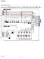
6-1. BLOCK DIAGRAM – SERVO SECTION –
117
CD DSP
IC101 (1/2)
XTAO
B
27
C
28
D
I-V AMP
29
RF
SUMMING
AMP
B
C
34
35
EQ_
IN
RFAC
VCA
EQ
RFACO
41
42
45
FOCUS
ERROR
AMP
D
AC_
SUM
FEO
46
24
RFACI
ASYMMETRY
CORRECTOR
XTAI
XTACN
EFM
DEMODULATOR
DIGITAL PLL
ASYI
ASYO
AOUT1
INTERNAL BUS
FILO
PCO
CLTV
FILI
26
A
CLOCK
GENERATOR
51 53 50 52 112
D +3.3V
A
XTSL
XPCK
DETECTOR
93
C4M
FILTER
D/A
CONVERTER
32K
RAM
ERROR
CORRECTOR
AOUT2
D/A
DIGITAL
INTERFACE
77
X171
16.9344MHz
78
95
CD-L
81
86
R-CH
A
(Page 29)
SELECTOR
TO SERVO AUTO
SEQUENCER
DIGITAL
CLV
PROCESSOR
102 105 104 107 115 98 99 96 97
LRCKI
BCKI
PCMDI
LRCK
BCK
PCMD
110 111 113 68
63 66 65
62 60 61
19 18 16 15 14
11
SDO0
100
SFSY/LRCKIB
SBSY/BCKIB
LRCKIA
BCKIA
SDI0
6
WFCK
XUGF
GFS
EMPH
OPTICAL PICK-UP
BLOCK
(KSM-213EDP)
CPU INTERFACE
SBSO
EXCK
SQSO
SQCK
22
SCOR
TEO
SENS
TRACKING
ERROR AMP
E
MDP
19
DATA
CLOCK
XLAT
20
E
SUBCODE
PROCESSOR
F
XRST
F
LASER DIODE
LD
PD
AUTOMATIC
POWER
CONTROL
Q10
36
LD
PD
APC LD
AMP
37
MP3 DECODER
IC301
I-SCOR
I-SENS
O-DATA
O-CLOCK
O-XLT
53 54 69 52 58
MOTOR/COIL DRIVE
IC251
M101
(SPINDLE)
M
16
15
CH4OUTF
CH4OUTR
MOTOR
DRIVE
CH4IN
24
27
OPOUT
OPIN+
2
I-MP3DATA
O-MP3DATA
O-MP3CLK
O-MICS
O-MILP
I-MP3_ACK
I-MP3_REQ
I-MP3_STBY
O-MP3RST
55
56
57
85
84
83
82
81
86
6
7
4
5
8
36
3
2
MIDIO
MICK
MICS
MILP
MIACK
PO11/BUCK/AD14
STANDBY
RESET
21 23
CH3FIN
MOTOR
CH3OUTR DRIVE
18
CH3RIN
SYSTEM CONTROLLER
IC601 (1/3)
23
A/D
CONVERTER
21
9
10
2-AXIS
DEVICE
(FOCUS) (TRACKING)
14
13
CH1OUTF
CH1OUTR
CH1FIN
COIL
DRIVE
CH1RIN
4
11
5
12
13
14
12
11
CH2OUTF
CH2OUTR
CH2FIN
COIL
DRIVE
CH2RIN
SFDR
SRDR
TFDR
TRDR
FFDR
FRDR
FOCUS/
TRACKING/SLED
SERVO DSP
MIRR,
DFCT, FOK
DETECTOR
FOK
MIRR
DFCT
COUT
SERVO
INTERFACE
SCLK
3
1
2
CD_OPEN_CLOSE 75
S601
DISC LID
OPEN DETECT
119
108
SERVO AUTO
SEQUENCER
6
7
O-XRST
CH3OUTF
SSTP
M
17
FOCUS/TRACKING/SLED
PWM GENERATOR
M102
(SLED)
O-XTCN 70
TEI
FEI
CD DSP
IC101 (2/2)
MUTE
TO CPU INTERFACE
20
• R-ch is omitted due to same as L-ch.
• SIGNAL PATH
73
7
S101
(LIMIT)
: CD PLAY
HCD-CZ1/NAS-CZ1
27
27
HCD-CZ1/NAS-CZ1
6-2. BLOCK DIAGRAM – ETHERNET SECTION –
J501
(ETHERNET)
TXD+
1
TXD–
2
NC
4, 5
3
6
7, 8
PULSE
TRANSFORMER
T501
16
14
15
RXD+
11
RXD–
NC
9
10
VDDRCV
38
(2.5V SUPPLY)
1
2
3
6
7
8
41 TX+
40 TX–
33 RX+
32 RX–
45 XO
X501
25MHz
D/A CONVERTER
IC505
ETHERNET CONTROLLER
IC502
ETHERNET INTERFACE
IC501
108
109
110
107
TXD0
TXD1
TXD2
TXD3
17
18
19
20
79
78
77
76
TXD0
TXD1
TXD2
TXD3
DOUT
BCLK
MCLK
LRCK
TXEN
TXC/REF_CLK
TXER
COL/RMII
CRS/RMII_LPBK
16
15
14
21
22
80
82
83
75
74
TXEN_N
TXCLK_N
TXER_N
COL_N
CRS_N
PIOC7 127
PIOC0 1
RXD0/PHYAD4
RXD1/PHYAD3
RXD2/PHYAD2
RXD3/PHYAD1
6
5
4
3
89
91
92
93
RXD0
RXD1
RXD2
RXD3
RXDV/PCS_LPBK
RXC
RXER/ISO
MDC
MDIO
9
10
11
2
1
87
86
84
94
95
RXDV_N
RXCLK_N
RXER_N
MDC
MDIO
2
3
4
1
DIN
BCKIN
MCLK
LRCK
VOUTR 8
PD# 30
RST# 48
2 PIOC1
3 PIOC2
• R-ch is omitted due to same as L-ch.
114 OSC1
• SIGNAL PATH
: ETHERNET
X502
24.576MHz
115 OSC1N
R-CH
SYSTEM CONTROLLER
IC601(2/3)
PDOWN
IICDATA
IICCLK
PIOC8 128
PIOC4/SDA/SDI1 102
PIOC5/SCL/SCLK1 101
XD0-15
8-14,16,26,
25,23-20,
18,17
2,3,5,6,8,9,
11,12,39,40,42, DQ0-15
43,45,46,48,49
MD0-15
53-56,42-37, MA1-19
50,48,47,45,
44,27,29,30,35
RAS
XRASN 68
CAS
XCASN 67
LDQM
XDQM0 73
UDQM
XDQM1 72
CLK
XSDCLK 69
CKE
XSDCKE 71
WE
XWEN 58
CS
XSDCSN 70
XOEN 57
21-24,
27-32,
20,19
MA1-12
RAS
CAS
LDQM
UDQM
CLK
CKE
WE
CS
17
16
14
36
35
34
15
18
A0-11
RAS
CAS
LDQM
UDQM
CLK
CKE
WE
CS
OE
FLASH MEMORY
IC504
X503
11.2896MHz
MD0-15
125 OSC0N
MA1-19
+2.5V REGULATOR
IC506
77 ETHER-PDOWN
37 I2C_DATA
38 I2C_CLK
SD-RAM
IC503
124 OSC0
EVER+3.3V
B
(Page 29)
17 MUTEB
18 SDIDEM
XA1-19
46 XI
E-LOUT
VOUTL 11
29-36,
38-45
DQ0-15
24-16,
8-1
A0-15
+2.5V
11 WE
28 OE
12 RST
RESETN 122
NRESET
HCD-CZ1/NAS-CZ1
28
28
76 ETHER-NRESET
HCD-CZ1/NAS-CZ1
6-3. BLOCK DIAGRAM – MAIN SECTION –
INPUT SELECT,
ELECTRICAL VOLUME
IC701
J201
6
16
R-CH
MUTING
Q761
E-LOUT
4
FM/AM
TUNER PACK
TU-L
TU-R
L-CH
R-CH
13
MUTING
Q731,831
MUTE CONTROL
Q860,862
OUTB
6 11
9 14
1
SP203
(WOOFER)
SP202
(FRONT TWEETER) R-CH
OVER LOAD
DETECT
Q261,262
SP201
(BACK TWEETER)
RELAY DRIVER
Q263
RY201
MUTE SWITCH
Q600
R-CH
J202
22
21
PHONES
MUTING SWITCH
Q607
RDS DATA
RDS CLK
RDS DATA
RDS CLK
SP103
(WOOFER)
MCU
I/F
5
TUNED
DI
DO
CK
CE
TUNED
DI
DO
CK
CE
AM
R-CH
+INB
STANDBYA
STANDBYB
R-CH
FM 75Ω
COAXIAL
3
+
SURROUND OR DPL BUFF
3
(Page 27)
(Page 28) B
OUTA
-1
CD-L
A
+INA
8
SP102
(FRONT TWEETER) L-CH
MUTEA
MUTEB
ANALOG IN
SP101
(BACK TWEETER)
POWER AMP
IC201
14 15
MAIN POWER
TRANSFORMER
T1
(AEP, UK)
F101
21
68 63 64 62 65
61 60
87
45
46
44 33 34 41 32
RDS_DATA
RDS_CLK
O-AMTE
GEQ_CLK
GEQ_DATA
LINE_MUTE
AMP_MUTING
AMP_STBY
SPK_RELAY
HP_IN
28 SIRCS
TUNED
PLL-DI
PLL-DO
PLL-CLK
PLL-CE
REMOTE CONTROL
RECEIVER
IC1011
A+3.3V
CD AVDD
CD DVDD
FL_DATA
FL_CLK
FL_CS
FL_RESET
MP3+1.5V
19 SELF_PROG
NETWORK
SDATA
SCK
CS
RST
51-25,
23-16
20-6
2G-16G
21-55
P1-35
FLUORESCENT
INDICATOR TUBE
FL1001
+7V
REGULATOR
IC112
D650
RECT
D111-114
+4V
REGULATOR
IC113
39 LED7
D135
D1251
D1201-1205
(PROFILE)
S1201-1205,1251,
S1252,1256,1257,
S1261,1263,1271
FRONT PANEL
KEYS
–30V
REGULATOR
Q131
FL–30V
8 STBY_LED
I/1
+4V
REGULATOR
IC114
ETHER+4V
RECT
D131-134
X1 14
LED DRIVE
Q1201-1205
X600
5MHz
97 LED1
|
|
93 LED5
X2 15
VF1
F1
VF2
RELAY DRIVE
Q1
POWER_RELAY 42
RY1
D606
100 KEY0
99 KEY1
98 KEY2
+3.3V
AC.CUT
5
1G
LED DRIVE
Q1272
20 KEY_INT
GRID DRIVE
Q1001
M+7V
D651
SYSTEM CONTROLLER
IC601(3/3)
RESET
DIG0
4
3-1,
64-53
+1.5V
REGULATOR
IC303
+9V
REGULATOR
IC111
ETHER+3.3V
D1271
8 7 6 5
AMP B-
A+9V
D+4V
27 29 30 31
FL DRIVER
IC1001
RECT
D101
+3.3V
REGULATOR
IC650
10 FLASHO
MODE CONTROL
Q603,604
AMP B+
F102
RM_INT
BUFFER
Q601,602
TO
POWER AMP
RDS DATA
RDS CLK
TUNED
DI
DO
CK
CE
(AEP, UK)
16
23
D605
D607
+3.8V
4 REGULATOR 5
IC604
D608
RESET
SWITCH
Q605, 606
VOLTAGE
DETECT
IC602
IC603
HCD-CZ1/NAS-CZ1
29
29
(AC IN)
SUB POWER
TRANSFORMER
T2
B-UP+3.3V
EVER4V
RECT
D613
• R-ch is omitted due to same as L-ch.
• SIGNAL PATH
: TUNER
: AUX IN
: CD PLAY
: ETHERNET
HCD-CZ1/NAS-CZ1
• Note for Printed Wiring Boards and Schematic Diagrams
Note on Printed Wiring Board:
• X : parts extracted from the component side.
• Y : parts extracted from the conductor side.
f
•
: internal component.
•
: Pattern from the side which enables seeing.
(The other layers' patterns are not indicated.)
Caution:
Pattern face side:
(Conductor Side)
Parts face side:
(Component Side)
Parts on the pattern face side seen from
the pattern face are indicated.
Parts on the parts face side seen from
the parts face are indicated.
Caution:
Pattern face side:
(Side B)
Parts face side:
(Side A)
Parts on the pattern face side seen from
the pattern face are indicated.
Parts on the parts face side seen from
the parts face are indicated.
• Indication of transistor
C
Q
These are omitted.
B E
Q
B
C
E
These are omitted.
• Circuit Boards Location
Note on Schematic Diagram:
• All capacitors are in µF unless otherwise noted. (p: pF)
50 WV or less are not indicated except for electrolytics
and tantalums.
• All resistors are in Ω and 1/4 W or less unless otherwise
specified.
•
f
: internal component.
• 2 : nonflammable resistor.
• 5 : fusible resistor.
• C : panel designation.
CD board
TUNER UNIT
ETHER board
MAIN board
Note:
The components identified by mark 0 or dotted line with
mark 0 are critical for safety.
Replace only with part number specified.
TOP PANEL board
SUBPS board
• A : B+ Line.
• B : B– Line.
• Voltages and waveforms are dc with respect to ground
under no-signal (detuned) conditions.
– CD Board –
no mark : CD PLAY
– Other Section –
no mark : TUNER
(
) : CD PLAY
〈〈
〉〉 : TAPE PLAY
{
} : REC
• Voltages are taken with a VOM (Input impedance 10 MΩ).
Voltage variations may be noted due to normal production tolerances.
• Waveforms are taken with a oscilloscope.
Voltage variations may be noted due to normal production tolerances.
• Circled numbers refer to waveforms.
• Signal path.
F : TUNER
J : CD PLAY
f : AUX IN
d : ETHERNET
FRONT PANEL board
FL board
PSAMP board
HCD-CZ1/NAS-CZ1
30
30
HCD-CZ1/NAS-CZ1
• See page 30 for Circuit Boards Location.
6-4. PRINTED WIRING BOARD – CD BOARD –
1
2
3
4
5
: Uses unleaded solder.
6
7
8
9
10
11
12
13
14
15
A
CD BOARD (COMPONENT SIDE)
M
B
M101
(SPINDLE)
CD BOARD
(CONDUCTOR SIDE)
3
1
4
5
IC303
C302
S101
(LIMIT)
R167
C305
C255
R405
R313
R404
C260
R351
28
C257
C315
C316
22
21
15
IC251
R302
R353
R354
17
R306
C258
C320
R253
1
7
8
14
IC301
R307
32
C308
C116
33
C14
R411
C211
C163
R163
C196
C182
C194
91
1
C172
C201
R166
120
C113
R113
R114
C114
R173
C174
R401
C213
R251
R407
R409
R191
F
R201
TP
(VC)
C251
R205
R162
R165
CN201
1
R303 C310
C184
C183
R402
48
R252
R410
C318
C317
R305
49
C309
FB301
C311
C307
R408
C259
C312
C210
R301
64
C314
E
M102
(SLED)
M
1 C313
16
R412
R406
D
R403
R419
C306
R352
C212
C
C252
C303
90
A
R182
MAIN
BOARD
CN700
(Page 36)
C115
C181
R172
X171
C112
C111
C17
R171
R112
R161
C161
30
CN101
R121
E
31
60
C124
C143
C133
C123
TP
(RFACO)
OPTICAL
PICK-UP
BLOCK
(KSM-213EDP)
I
HCD-CZ1/NAS-CZ1
31
31
21
1-861-619-
C122
C134
27
R151
(21)
R10
Q10
R132
R133
R131
R142
C141
1-861-619-
C151
R181
R204
61
C132
R143 R141
21
C16
C131
C125
C15
C185
C11
R13
C209
H
C186
C162
C18
R11
R12
C203
R111
C10
C171
G
IC101
C195
C142
R203
(21)
HCD-CZ1/NAS-CZ1
• See page 45 for Waveforms.
6-5. SCHEMATIC DIAGRAM – CD BOARD –
• See page 46, 47, 48 for IC Block Diagrams.
C131
100p
R151
0
TP125
RFACI
C133
0.01
C141
0.1
R133
180k
R141
4.7k
R132
10k
C15
0.1
R121
15k
C17
220
4V
R12
100k
C123
0.1
C122
0.1
JPO10
APC
C16
1
R10
3.3
VCC
TP424
IOP2
C11
10
Q10
2SA2119K
R11
0
AUTOMATIC
IC301
TC94A34FG-002
MIDIO
MIACK
MICK
MIDIO
MILP
R419 100
MILP
AD8
R403 100
MICS
R402 100
MP3STB
C161
0.1
MP3RST
C171
R171
X171
22p 16.9344MHz 470
R173 0
C181
0.1
AVDD4
RFDCO
PDSENS
LD
EG_IN
PD
NC
RFC
AVSS4
RFACI
RFACO
BIAS
AVDD3
VCTL
ASYI
ASYO
VPCO
AVSS3
CLTV
FILI
PCO
FILO
AVDD5
EMPHI
TEO
IOVDD2
TEI
DOUT
F
TEST
E
C174
0.1
IOVSS2
AVSS0
NC
AVDD0
TP18 T-
F-
TP19 F-
TFCN101
16P
3300p
3300p
C114 470p
F
C115
0.1
CD DSP
XTAO
IC101
CXD3059AR
TP428 FRDR
FRDR
TP429 FFDR
FFDR
TP430 TRDR
TRDR
TP431 TFDR
TFDR
FRDR
FFDR
XVDD
TRDR
AVDD1
TFDR
AOUT1
SRDR
VREFL
SFDR
AVSS1
IOVSS1
SFDR
C183
22
6.3V
TP426
SW-
C195
0.1
TP425 SW+
C316
0.0022
SSTP
AVSS2
C186
470p
AOUT2
R182
100
TP432 MDP
C184
22
6.3V
VREFR
MDP
AOUT2
LOCK
(LIMIT)
FOK
COUT
MIRR
NC
C4M
WDCK
VDD
SCOR
C2PO
GFS
XPCK
XUGF
ATSK
WFCK
SCLK
SENS
DFCT
VDD
CLOCK
XLAT
VSS
DATA
SYSM
XRST
EXCK
SBSO
SQCK
SQSO
XTACN
XTSL
LMUT
NC
RMUT
IOVSS0
IOVDD0
C203
100
10V
S101
MDP
VSS
NC
C162
0.1
+1.5V REGULATOR
VIN
IC303
BH15FB1WG
C210
0.1
C194
0.1
R165
0
TP422
MP3GND
C163 0.1
TP433
MP3VDD
C196
0.1
SCOR
SENS
CLOCK
XLT
XRST
DATA
R191
0
XTACN
C303
0.1
R166
1k
R162
47k
R163 100
GND
T-
IOVDD1
XVSS
AVDD2
STBY
T+
C116
100
10V
SRDR
R181
100
C201
100
10V
NC
F+
TP17 F-
C112 470p
C113
NC
XTAI
C182
0.1
VOUT
C111
AOUT1
C308
47
4V
TP16 F+
T+
E
R172
1M
C172
27p
C185
470p
R313
220
F+
FEI
TEST1
VCOI
VSSP
MIMD
TEST
VSSX
XI
VDDX
FEO
R114 15k
R161
100
C317
0.01
C315
0.1
VDD
JPO103 TEI
VDDP
R306
0
VC
DOUT
C318
0.01
C14
0.1
A
BCK
R113 1k
RESET
XO
CKO/PO13/AD16
VDD
VSS
AD0/PO00
AD1/PO01
AD2/PO02
AD4/PO04
AD3/PO03
B
R111 1k R112 15k
R305
100k
C302
0.1
D
JPO102 FEI
R301
100k
FB301
NC
C
EMPH
STANBY
R401 100
PD
A
MICS
C305
220
4V
F
AGND
TP177
VC
MICK
R302 10k
MP3 DECODER
AD9
C309
0.1
C
TP105 BCK
R353
100
MIACK
C312
0.1
B
TP14 C
VR
C
PCMD
C306 0.1
R404 100
C311
0.1
A
TP13 B
C
TP15 PD
TP104 PCMD
VSS
R405 100
C313
0.1
TP12 A
B
TP102 F
B
VDDT
SRMSTB
C314
47
4V
A
D
LRCK
VSS
PO10/CCE/AD13
PO05
AD5/
AC_SUM
LRCKI
TP103 LRCK
R351
100
PO11/BUCK/AD14
VDDM
PO06/AD6
DDVRSEN
PCMDI
DDVROUT
SDI0
SDO0
PO07/AD7
NC
TP427 PCMDI
R352
100
DDCR
TXO
SBSY/BCKIB
SFSY/LRCKIB
VDD
VSS
IRQ/FIO
CKI/CLOCK/
PIO0/SDI2/IO0
PIO2/IO2
PIO3/IO3
PIO1/SDI3/IO1
BCKI
BCKIA
PO08/AD11
C310
0.1
D
F
R354
100
LRCKIA
PO9/AD12
AD10
TP11 D
C18
1000p
LRCKO
VDDT
E
D
LD
DATA
BCKO
R303
100k
TP10 E
SDI1/
AVSS5
MP3REQ
PIO4/FI1/BUS0/IO4
SDO3/OE
PIO7/BUS3/IO7
PO12
PIO5/FI2/BUS1/IO5
CS/RAS/
AD15/CAS/
PIO6/FI3/BUS2/IO7
SDO2
E
POWER
CONTROL
WE/SDO1
VC
R13 1
TP124
RFACO
C143
0.1
R131
1M
C125
0.1
C124 330p
R307
10k
R142 1k
R203
0
C307
0.1
C134
0.1
R143
3.3k
C132 0.47
C151
100
10V
C10
10
TP423
IOP1
C142 1500p
CN201
27P
M+7V
TP186 MVDD
MIDIO
TP405 MIDIO
MIDIO
MILP
TP406 MILP
MILP
MICS
TP407 MICS
MICS
TP408 MP3RST
MDP
R251
10k
R252
22k
C251
6800p
JPO004
MDP
TP418
GAIN_SW
R253
10k
C259
0.1
C213
22p
MP3(3.3V)
MP3RST
R167
100
T-
MICK
T+
MIACK
TP404 MICK
F+
TP403 MIACK
MICK
F-
MIACK
FRDR
MP3REQ
FFDR
TP402 MP3REQ
TRDR
MP3STB
MP3REQ
TFDR
TP401 MP3STB
TP421 DGND
TP187 MGND
MP3STB
TP420 AGND
MGND
TP436 AVDD
MGND
C258
0.1
MP3RST
C320
0
MP3GND
R205 0
SCOR
TP417 SCOR
R411 100
SCOR
SENS
TP416 SENS
R410 100
SENS
CLK
TP415 CLK
R409 100
CLOCK
XLT
TP414 XLT
R408 100
DATA
TP413 DATA
R407 100
DATA
XRST
TP412 XRST
R406 100
XRST
XTCN
TP419 XTCN
R412 100
XTACN
AVDD(3.3V)
TP434 AVDD
ROUT
TP410 ROUT
AOUT2
TP411 LOUT
AOUT1
TP409 DOUT
DOUT
C209
0.01
C257
0.1
CH1OUTF
CH1OUTR
POWVCC
CH2OUTF
CH2OUTR
GND
CNF4
CH2RIN
CH2FIN
CH1FIN
CH1RIN
SW
OPIN+
XLT
C252
0.1
MOTOR/COIL
C211
220p
CH4OUTR
CH4OUTF
CH3OUTF
CH3OUTR
POWVCC
GND
MUTE
CH3RIN
CH3FIN
CH4CAPA
CH4IN
OUTVREF
IC251
BA5947FM
OPOUT
DRIVE
PREVCC
(Page 37)
OPIN-
R201
C212
22p
C255
0.1
C260
220
10V
LOUT
DOUT
DVDD(3.3V)
SFDR
DGND
TP435
DVDD
R204
SRDR
AGND
TP250 SPTP251 SP+
M101
(SPINDLE)
TP252 SL+
TP253 SL-
M102
(SLED)
HCD-CZ1/NAS-CZ1
32
32
HCD-CZ1/NAS-CZ1
• See page 30 for Circuit Boards Location.
6-6. PRINTED WIRING BOARD – ETHER BOARD –
2
3
4
5
6
8
9
ETHER BOARD (SIDE A)
97
FB507
FB512
FB513
FB508
R530
48
C520
C519
C521
C517
R510
K
A
A
K
K
A/K
R506
R505
C503
R507
R508
R501
R502
C501
R503
R504
C514
C504
C511
K
A
A/K
C516
A
A/K
C522
R553
1
J501
(ETHERNET)
C515
R515
R516
R534
R511
R529
R514
A/K
R552
R554
T501
PULSE
TRANSCEIVER
24
C523
R551
12
37
C525
D514
13
36
1
R527
IC501
R512
C546
C527
C529 C528
D513
R513
C532
R531
R521
C533
C535
FB503
24
25
FB505
C536
C518
E
C548
C549
X502
R546
R526
R532 C539
R517
C565
96
C558
IC504
D512
65
1
R522
R523
R524
R525
R518
R533
FB504
R561
C567
C530
D511
64
R559
C538
C566
20
FB506
R548
C568
C564
R542
C534
C531
C544
C541
R539
R538
C537
R537
C540
C550
10
25
C552
C543
X503
11
C557
48
C510
C551
C569
IC505
128
IC502
FB510
IC506
D503
C563
1
26
C507
1
R519
D504
R541
C547
C542
R528
IC503
32
FB509
3
C509
FB511
R540
33
F
15
C559
FB518
50
25
14
C508
FB517
C554
D
13
C556
FB502
D502
FB516
FB520
FB519
FB515
D501
1
C555
12
15
CN501
FB521
1
D505
B
C
11
ETHER BOARD (SIDE B)
D506
C553
10
MAIN BOARD
CN651
(Page 36)
B
A
7
R545
1
: Uses unleaded solder.
C505
R574
R571
R572
R573
X501
R509
C524
C545
C513
C512
EP501
G
11
11
1-866-454-
1-866-454-
(11)
(CHASSIS)
• Semiconductor Location
HCD-CZ1/NAS-CZ1
33
33
Ref. No. Location
Ref. No. Location
D501
D502
D503
D504
D505
D506
D511
D512
D513
D514
E-12
IC501
IC502
IC503
IC504
IC505
IC506
E-5
D-5
C-3
C-14
D-7
C-11
B-4
B-4
B-9
B-9
B-4
B-4
F-12
F-12
E-12
(11)
HCD-CZ1/NAS-CZ1
• See page 45 for Waveforms.
TP506
TP505
MA1
OE
ROMCS
MD0
MD9
MD8
MD2
MD1
MD10
0.1
MD3
MD11
C559
MD5
MD4
MD13
MD12
MD7
MD6
MD14
MA17
MD15
MD1
MD0
0.1
MD2
MD4
MD3
0.1
MD5
C554
MD6
MD7
WE
C555
MA12
MA2
MA1
C550
0.1
C514
0.001
2kV
R571
75
C553
0.1
C558
47
6.3V
C556
10
16V
R519
10k
TP507
A0
CE
FB510
0
A2
A1
OE
DQ0
DQ8
VSS
A3
A4
A5
A6
DQ9
DQ1
A7
A17
DQ10
DQ2
A18
RY/BY
DQ3
NC
DQ4
VDD
DQ11
RST
NC
WE
DQ5
DQ12
NC
DQ6
DQ13
A8
A9
DQ14
NC
A12
A13
A14
A15
A10
VSS
VSS
DQ0
DQ15
DQ7
DQ1
VDD
DQ14
DQ15/A-1
VSSQ
VSSQ
FLASH MEMORY
IC504
MBM29LV800BA-70P
A11
DQ2
DQ13
A16
DQ3
DQ12
IC503
MSM56V16160F-8TK
-FM1
BYTE
DQ4
DQ5
DQ10
VDDQ
VSSQ
VSSQ
VDDQ
DQ6
DQ9
DQ11
DQ7
DQ8
WE
VDDQ
VDDQ
CAS
NC/RFU LDQM
CLK
UDQM
CS
RAS
CKE
A10/AP
A11-BA
NC
A9
A8
A1
A0
A7
A6
A3
VDD
VSS
A4
C545
0.1
A5
R574
75
A2
SD-RAM
R573
75
EP501
• See page 50 for IC Pin Function Description.
TP509
TP502
TP504
MA11
MA4
TP508
R572
75
MA3
LED2-
LED2+
(ETHERNET)
• See page 49 for IC Block Diagrams.
CHASSIS_GND
NC
LED1-
LED1+
NC
NC
NC
RXD-
TXD-
TXD+
J501
8P
RXD+
6-7. SCHEMATIC DIAGRAM – ETHER BOARD –
C503
0.1
R506
100
MA2
MA3
MA4
MA5
MA6
MA7
MA8
MA18
MA19
WE
MA9
MA10
MA11
MA13
MA12
MA14
MA16
MA9
MA8
MA10
MA7
MA6
MA5
MA15
MA14
MA15
MD14
MA13
MA12
MD15
R530
100
MA19
C527
0.1
TP513
R505
100
R508
100
TP515
R507
100
C548
0.1
C546
0.1
TP514
R501
100
R502
100
R561 47
R504
100
R559 47
R503
100
D513
DAN217
-T14
MD13
MA11
C549
0.1
R529
10k
D512
DAN217
-T14
MD12
C552 0.1
MD11
MD10
MA2
MA1
MD9
MA3
OE
MA4
RXRD-
ROMCS
WE
MD8
MA10
CT
C501
0.1
MA9
RX+
RD+
RCT
C504
0.1
MA8
NC
NC
D511
DAN217
-T14
C518
0.1
MA7
NC
NC
C505
100
6.3V
MA6
TXTD-
FB508
0
C551
0.1
MA5
TX+
CMT
TRANSFORMER
TD+
T501
H1260
PULSE
TCT
(CHASSIS)
TP512
TP511
XCASN
XRASN
R514
10k
C519
0.1
TP503
INT#/PHYAD0
LED0/TEST
GND
XSDCKE
XA23
XD8
XDQM1
XA18
XD9
XA17
XDQM0
C525
0.1
VDDIO
XA21
XA20
XA19
VDD_IO
XA9
XA10
XA7
XA8
XA6
XA5
XA15
XA14
VDDCORE
GND
GND
XA12
XA13
XA11
XA0
XA1
XA2
XA3
XA4
XOEN
XWEN
XA16
XD10
XD11
XD12
CRS/RMII_LPBK
TXD2
XD13
COL/RMII
TXD1
GND
TXD3
TXD0
TXD2
IC501
KSZ8721BL
ETHERNET CONTROLLER
XD14
IC502
ML7201
XD15
TXEN_N
C528
0.1
TXD1
MD8
MD9
C544
0.1
MD10
MD11
MD12
MD13
MD14
MD7
TXD0
TXCLK_N
TXEN
TXER_N
XD6
RXER_N
XD5
VDD_CORE
XD4
SDO1
RXD1
PIOC6
GND
ETHER-GND
MD0
FB515
ETHER+3.3V
R528
10k
FB516
D-GND
PLLGND
C543 47 6.3V
D-GND
IICCLK
C542
0.1
TEST2
PIOB5/DATAIN
IICDATA
C547
0.001
PIOC1
OSC0N
GND
OSC0
TDO
RESETN
TDI
TMS
TCK
NTRST
GND
OSC1N
VDD_IO
OSC1
PIOC2
TEST0
MCLK
BCLK
PIOA6/RXD
DOUT
SAICLK
LRCK
MDIO
PIOA7/TXD
VDD_CORE
MDC
TP517
CN501
15P
MD1
PLLVDD
RXD3
C521
0.1
D501
1SS355
MD2
PLLMODE
RXD2
C524
10
16V
MD3
XD0
PIOC7
C523
0.1
MD4
XD1
VDD_IO
FB503
0
D502
1SS355
MD5
XD2
RXD0
C517
10
16V
(CHASSIS)
MD6
XD3
SDA/SDI1
SCL/SCLK1
GND
MCS
GND
RXDV_N
MSK/SCLK0
RXCLK_N
C522
100
6.3V
MDI/SDI0
VDDC
MDO/SDO0
C529
0.1
TXER
RXER/ISO
RXDV/PCS_LPBK
GND
VDDIO
MDIO
MDC
RST#
RXD0/PHYAD4
VDDPLL
RXD1/PHYAD3
0
RXD2/PHYAD2
FB502
C516 0.1
R510
10k
RXD3/PHYAD1
XI
RXC
XO
X501 25MHz
C513
10p
D505
1SS355
TEST1
R509 680
C512
10p
D506
1SS355
MD15
XD7
VDD_IO
TXC/REF_CLK
GND
MA16
VDD_IO
CRS_N
TXD3
ETHERNET INTERFACE
GND
XA22
COL_N
TX+
VDDTX
MA17
GND
XSDCSN
GND
TX-
C511
0.1
MA18
XSDCLK
TP501
LED1/SPD100
LED2/DUPLEX
VDDRCV(2.5V Supply)
LED3/NWAYEN
VDDRX
PD#
RX-
RX+
FXSD/FXEN
GND
GND
REXT
VDD_IO
VDD_IO
R534
13k
XROMCSN
GND
R513
10k
PIOA0/XIOCSN
XBSN0
C520
0.1
C515
100
6.3V
PIOB6/XRAMCSN
R511
13k
PIOB7/XWAIT
D514
DAN217-T14
XBSN1
TP516
R512
10k
PDOWN
NRESET
PIOC0
FB517
FB511
D-GND
FB518
IC506
BA25BC0FP-E2
TP521
TP520
(Page 38)
A-GND
R539
100
TP518
R515
10k
TP519
R516
10k
A3.3V
FB519
+2.5V REGULATOR
LOUT
FB520
DA-GND
TP522
TP523
C541
0.1
TP525
C532
0.1
R538
100
ROUT
FB521
FB509
0
O
G
DA-GND
I
R541
100
R548
10k
C537 0.1
FB506
FB507
C535
10p
R533 560
C534
0.1
C536
10p
R537
1k
FB505
0
R518
1M
R532
1k
X503
11.2896MHz
C538
18p
C539
18p
R531
0
R540 100
C568 0.1
C530
0.1
C531
10
16V
C510
0.1
C509
100
6.3V
C540
0.1
C508
0.1
C507
100
6.3V
R542 10
R517
1M
TP524
FB513
R546
4.7k
R527
47
X502
24.576MHz
C557
0.1
R526
47
FB512
R545
4.7k
C569
10
16V
C567
0.1
C533
100
6.3V
C571
0.1
FB504
0
VMID
VOUTL
AGND
C563
10
16V
AVDD
VOUTR VREFN
MODE
VREFP
DVDD
MUTEB
CSB-WL
DGND
ZERO
MCLK
LATI2S
SCKDSD
SDIDEM
BCKIN
LRCIN
IC505
WM8728
C572
0.1
R552
10k
DIN
R553
10k
R551
0
C564
0.1
D/A CONVERTER
R554
0
R525
100
TP531
R524 100
R523 100
R522 100
R521
0
C565
10
16V
C566
0.1
HCD-CZ1/NAS-CZ1
34
34
C562
0.1
D504
D503
1SS355 1SS355
HCD-CZ1/NAS-CZ1
6-8. PRINTED WIRING BOARD – MAIN BOARD (COMPONENT SIDE) –
1
A
2
3
4
5
• See page 30 for Circuit Boards Location.
6
7
8
: Uses unleaded solder.
9
10
11
12
MAIN BOARD (COMPONENT SIDE)
B
C
D
E
F
G
H
I
J
K
11
1-866-455-
HCD-CZ1/NAS-CZ1
35
35
(11)
HCD-CZ1/NAS-CZ1
• See page 30 for Circuit Boards Location.
6-9. PRINTED WIRING BOARD – MAIN BOARD (CONDUCTOR SIDE) –
1
2
3
4
5
6
A
7
8
FL BOARD
CN1001
(Page 43)
F
MAIN BOARD (CONDUCTOR SIDE)
: Uses unleaded solder.
9
10
FRONT PANEL
BOARD
CN1201
(Page 41)
E
11
12
13
14
PSAMP BOARD
CN103
(Page 39)
D
• Semiconductor
Location
C717
CN601
FB602
R632
R633
E
R611
R615
R687
R691
R689
R685
R677
R690
R688
R686
R684
C622
R676
R721
R722
C661
R712
C651
R667
R711
R670
C614
R661
R663
R710
R662
R660
R659
R653
R640
R644
51
R637
50
(AEP, UK)
R631
4
R622 R623
C620
CN651
R620
3
C606
C602
5
Q602
IC602 1
D601
CD BOARD
CN201
(Page 31)
R628
E
C604
NC
R672
31
R626
B
E
E
R730
Q761
Q861
R651
R654
R649
R646
R639
ETHER BOARD
CN501
(Page 33)
(US)
E
R612
R613
R731
C600
C601
R734
R614
R733
Q600
C710
C707
R609
R610
R735
R635
R606
R732
G
R629
R605
C605
AM
CN650
H
R851
R852
J
C907
L751
C805
C815
C911
C808
C913
42
1
C810
R953
R952
R903
E
C812
C860
C813
C811
C908
K
R950
SUPPLIED WITH THE
ASSEMBLED BLOCK
R862
C809
C912
E
FM/AM
TUNER PACK
E
R750
C807
R753
R804
Q860
C904
R900
Q731
Q831
C910
FM 75Ω
COAXIAL
(AEP, UK)
R802
C806
IC701
CN751
R751
C816
C801
C818
C803
Q862
R901
E
21
C804
C905
R854
R853
22
R752
C909
C900
C906
FB750
FB751
C814
PSAMP BOARD
CN202
(Page 39)
C752
C802
C817
C902
C903
C
C800
R800
C901
R803
I
R902
FB802
R801
FB803
FB801
R860
R951
11
1-866-455-
HCD-CZ1/NAS-CZ1
36
36
IC601
IC602
IC603
IC604
IC650
IC701
E-8
F-4
E-6
D-4
C-11
I-7
Q600
Q601
Q602
Q603
Q604
Q605
Q606
Q607
Q731
Q761
Q831
Q860
Q861
Q862
G-7
F-6
F-6
D-6
C-6
D-6
D-6
C-9
J-3
G-6
J-3
J-10
G-6
J-10
C623
R675
30
R624
D600
C608
81
R627
R645
A
D602
C610
R666
Q603
R652
R642
R630
D603
Q601
CN605
IC601
80
R604
C607
R702
D651
R638
R618
R698
R700
R701
R634
C611
C609
R697
R699
C603
D604
3
R607
D608
C629
R703
X600
R636
C631
E
100
1
R647
4
1 3
1
C630
FB603
Q604
5
C632
Q607
FB600
R619
D606
R641
IC603
IC650
R668
R603
D607
E
Q606
E
D605
R681
C612
Q605
C713
R707
E
R705
R704
R602
CN700
E
C616
FB705
R669
D609
C618
FB707
FB704
FB706
C712
FB703
3
R674
IC6041
C615
R673
C708
FB702
R665
R680
4
R679
E
C613
C624
5
C706
FB701
D
C640
C617
C705
C634
D650
C633
R664
C626
C621
C703
1
R706
C700
1
FB700
F
FB612
FB611
C704
C635
CN600
14
D621
S601
DISC LID
OPEN DETECT
C701
C
C702
CN603
G
FB613
4
FB614
SUBPS BOARD
CN115
(Page 39)
FB615
B
Ref. No. Location
D600
F-5
D601
F-5
D602
F-5
D603
E-5
D604
E-5
D605
E-5
D606
E-4
D607
E-4
D608
E-4
D609
D-5
D613
B-4
D621
C-5
D650
C-10
D651
E-11
FB601
R650
EPT701
(CHASSIS)
FB616
CN602
D613
R648
C628
C714
(11)
HCD-CZ1/NAS-CZ1
6-10. SCHEMATIC DIAGRAM – MAIN BOARD (1/2) –
L751 100µH
6
(1/2)
R753
1k
10
7
R752
100k
5
9
IC701
M61529FP-D60G
C752
100
16V
1
C813
100
10V
C908
0.047
2
3
R903
10k
CN751
9P(US)
C913 10 50V
11P(AEP,UK)
C912 10 50V
C811
10 50V
C911 10 50V
C810
10 50V
C910 10 50V
C809
10 50V
65
CE
64
DO
62
FM 75Ω
4
C812
10
50V
(Page 38)
8
R750
100k
CK
63
COAXIAL
DI
FM/AM
TUNER PACK
L-CH
FB751
SUPPLIED WITH
+B(+9V)
THE ASSEMBLED
R-CH
0
R751 1k
BLOCK
FB750
0
R901
2.2k
GND
AM
68
C808
0.022
C907
0.022
R803
2.2k
TUNER
DATA
RDS DATA
C900
10
50V
CLK
RDS CLK
(AEP,UK)
CN700
27P
C807
0.022
C906
0.022
R804
10k
C806
0.047
R900
10k
C904
0.0047
FB700
0
C815
10
50V
C805
0.0047
C905
0.047
M+7V
MGND
FB701
0
MGND
MP3STB
81
C700
100
10V
C701
0.1
MP3REQ
56
MIDIO
C816
0.1
C802
0.022
R902 47k
R802
47k
84
MILP
85
MICS
FB702
C814
10
50V
0
MP3(+3.3V)
INPUT SELECT,
86
MP3RST
FB703
46
C901
10
50V
58
SCOR
52
SENS
C800
100p
54
CLK
C817
470
16V
ELECTRICAL VOLUME
0
MP3GND
(Page 32)
C803
0.022
C902
0.022
57
MICK
C818
0.1
C903
0.022
83
MIACK
C804
10
50V
C909
10 50V
82
C801
100p
R800
100
R801
1k
45
11
69
XLT
53
DATA
73
XRST
R854
1k
70
XTCN
R862
0
12
Q731,831
MUTING
FB704
13
AVDD(+3.3V)
FB705
AGND
R951
1k
Q831
2SC3624
LOUT
DGND
R707 100
DOUT
Q860
DTA114EKA
R953
10k
ROUT
FB706
R851
10k
C707
2.2
50V
DVDD(+3.3V)
R860
100k
FB707
R950
1k
FB803
0
R952
10k
R852
10k
0
FB801
0
Q761
2SC3624
C708
0.1
C706
100
10V
Q860,862
Q861
2SC3624
R734
10k
R853
1k
R731
4.7k
R733
4.7k
R-CH
FB802
MUTING
Q862
DTC114EKA
MUTING CONTROL
R730
1k
CN650
15P
R735
10k
Q761,861
C860
1
50V
Q731
2SC3624
AGND
R732
1k
L-CH
32
HP IN
43
C710
2.2
50V
NC(HP MUTE)
33
(Page 38)
C705
100p
AMP MUTE
34
AMP STANDBY
41
PROTECTOR
42
C703 100
10V
POWER RELAY
C704 0.1
(Page 40)
EVER+4V
14
UNREG-SUB
SUB-GND
15
AUX-R
AGND
C702
100p
AUX-L
16
17
C717
0.1
EPT701
C714
0.1
(CHASSIS)
HCD-CZ1/NAS-CZ1
37
37
C712
0.1
C713
100
10V
HCD-CZ1/NAS-CZ1
• See page 45 for Waveforms.
6-11. SCHEMATIC DIAGRAM – MAIN BOARD (2/2) –
• See page 48 for IC Block Diagrams.
• See page 52 for IC Pin Function Description.
(2/2)
1
D651 EC10DS2
D650 EC10DS2
2
3
4
5
6
7
O
G
I
8
C634
1000
16V
C630
0.1
64
65
68
R659
1k
77
76
75
70
69
63
R653 100
R654 100
61
62
58
R651 1k
57
R640 1k
60
56
R631 100
R637 100
53
R629 100
R639 100
52
54
R627 1k
61
60
C651
1000p
DATA
C661
1000p
IC650
TA78033LS
CLK
(Page 37)
C629
220
10V
73
9
R668
10k
C614
0.01
R646
1k
DA-GND
C620 0.001
C623 0.001
R672 100
R676 10k
R670
100
R675 100
CN651
15P
R650 100
R649
1k
10
R667
100
R663 10k
R710
4.7k
(AEP,UK)
R660 10k
R711
100
R644
1k
R635 100
R721
100
R648
1k
R662 100
R712
100k
R661 100
+3.3V REGULATOR
R722
100k
CN600
14P
VF
VF
FL-30V
(US)
ROUT
FL-GND
DA-GND
LED6
NO_
USE12
NO_
USE13
FLASH1
ETHER-PDOWN
ETHER-NRESET
O-CD_ON
BVDD
O-XRST
BVSS
O-XTCN
O-XTL
TUNED
NO_USE11
NO_USE10
PLL-CE
PLL-DI
PLL-DO
PLL-CLK
RDS_CLK
RDS_DATA
NO_USE9
I-SCOR
O-MP3CLK
I-MP3DATA
NO_USE5
R615 100
O-MP3-STBY
81
UCOM-GND
R702 1k
82
ETHER+4V
R701 1k
83
D+4V
R700 100
84
MGND
R699 100
85
M+7V
R698 100
86
AGND
I-MP3-REQ
I-MP3-ACK
GEQ_DATA
IICDATA
O-MICS
R613 100
GEQ_CLK
O-MP3RST
LINE_MUTE
ETHER+3.3V
MUTING
42
R610 100
41
R609 1k
HP_MUTE
DEVICE_ON_OFF
SYSTEM CONTROLLER
POWER_RELAY
ST-GND
NO_USE14
IC601
µPD703261YGF-S06
-JBT-A
SPK_RELAY
SWITCH
ETHER-GND
O-AMUTE
C631
0.001
NO_USE15
NO_USE3
NO_USE16
LED7
NO_USE17
R607 1k
39
R691 100
R620 47
12C_CLK
LED5
12C_DATA
LED4
R619 47
R602
10k
C600
22p
EVDD
34
R606 100
33
R605 100
C604
0.1
SO
FLMD0
25
MODEL
DEST
AVREF0
AVSS
NO_USE1
SOFT-CHECK
AVREF1
STBY_LED
NO_USE2
FLASH0
VDD
REGC
VSS
X1
X2
RESET
XT1
XT2
SELF_PROG
KEY_INT
RM_INT
(CAN'T_USE)
AC_CUT
FLASH_CLK
99
100
KEY0
R684
1k
C602
0.001
*R679
R704
10k
22k(US)
Q601
2SC1623
24
R618
470k
Q602
2SC1623
4.7k(AEP,UK)
CN601
15P
R622
47k
97
R642
10k
R665 100
R638 1k
R634 100
R623
47k
R626
100
R636 100
R624
100
R628
1k
R630 100
RESET
FB600
R652
100k
LED2
95
LED3
94
(US)
R664
10k
C622
0.1
LED4
LED5
GND
R681
47k
FB601
0
FB602
98
KEY2
99
RESET SWITCH
X600
5MHz
KEY1
100
FB603
Q603
DTC114EKA
R633
220
IC603
D604
1SS355
IC602
PST3629
STBY-LED
Q603,604
MODE CONTROL
LED6
39
SN74AHC1GU04DCKR
LED7
Q605
DTC114EKAQ606
T146
2SC1623
CN602
13P
FB611
D603
1SS355
C616
0.1
DGND
R669
47k
FB612
0
EVER+3.3V
Q604
DTA114EKA
(Page 37)
D GND
47
R645 4.7k
D602
1SS355
0
R666
470
R680
47k
D601
1SS355
28
R632
10k
C605
10
50V
C617
0.22
C606
0.1
C608
0.22
C610
0.1
C611
0.1
R674
100k
D609
1SS355
C624
0.1
SITCS
31
C626
1000
6.3V
FL-RESET
30
FL-CS
FB613
29
0
FL-CLK
27
FL-DATA
FB614
DGND
FL-30V
GND
CTL
D607
1SS355
D621
1SS355
VF
GND
14
15
VF
IN
INVERTER
FB615
R673
100k
OUT
VOLTAGE DETECT
FB616
D606
1SS355
+3.8V REGULATOR
D605
1SS355
16
17
C615
0.01
C618
47
10V
C621
0.1
C640
220
16V
C627
C628
0.1
GND
CD_OPEN_CLOSE
SUBAC
C609
0.22F
5.5V
SUBAC
C607
0.1
CN603
4P
S601
DISC LID
OPEN DETECT
HCD-CZ1/NAS-CZ1
38
38
0
D+3.3V
D613
EC10DS2
IC604
NJM2870F38(TE2)
D608
1SS355
(Page 42)
KEY0
13
D600
RB501V-40TE-17
GND
0
LED+7V
Q605,606
24
25
26
10
75
LED1
96
C612
0.1
R677
47k
R641
47k
27
29
BUFFER
30
28
Q601,602
R647
1k
93
C613
4.7
50V
11
12
98
R685 1k
26
10
97
KEY1
R679 *
SCK
FLASH_DI
FL_DATA
FL_
CS
FL_
CLK
GND
SIRCS
FL_RESET
R603
100
FLASH_DO
HP_IN
SI
96
R687 100
KEY2
R604 1k
VDD
95
R688 100
R686 1k
31
NC
94
R689 100
LED1
AMP_MUTING
CN605
7P
93
R690 100
LED2
AMP_STBY
32
Q607
DTA114EKA
MUTING SWICTH
LED3
C603 0.1
EVSS
C601
22p
C633 0.001
Q600
DTA114EKA
D-GND
R611 100
A+9V
R697 100
R612 100
43
C632 0.001
45
IICCLK
D-GND
(Page 40)
O-MILP
R614 100
46
R706 10k
47
DGND
R703
100
R705 10k
77
PDOWN
CD_OPEN_CLOSE
76
NRESET
O-MP3DATA
O-CLOCK
NO_USE6
D-GND
(Page 34)
O-DATA
NO_USE7
A+3.3V
NO_USE8
A-GND
I-SENS
MP3-GND
LOUT
(Page 40)
C635
100
10V
(Page 44)
HCD-CZ1/NAS-CZ1
6-12. PRINTED WIRING BOARDS – POWER SECTION – • See page 30 for Circuit Boards Location.
5
6
7
8
R–CH
BLK
BLU
SP202
(FRONT TWEETER)
BLK
BLK
RED
RED
SP203
(WOFFER)
RED/BLK
RED/BLK
4
2
RED
C243
JW130
(CHASSIS)
JW122
R152
C117
JW153
JW129
R153
C118
EP202
C119
R823
R151
C115
IC111
C103
C104
JW160
C203
JW161
4
C204
C114
FB241
JW121
C229
C343
JW132
R329
C330
JW135
R228
C232
C231
C230
R227
JW154
R229
C116
R328
FB341
JW131
Q261
RY201
JW139
JW140
JW148
JW141
C224
Q262
1
D821
(CHASSIS)
JW133
R262
C202
JW136
C261
C201
JW138
Q263
JW146
C226
C325
R325
C324
JW152
JW155
R327
R226 R326
R225
C225
C266
EP201
R261
1
JW147
C321
JW158
JW159
C262
JW145
C221
C
JW137
C223
C326
JW144
JW142
R321
R223
R224
JW151
R221
JW149
R322
D261 R263
C263
1
15
R324
EP101
R264
CN202
1
R222
C323
C268
C265
C264
JW150
C251
R251
R252
2
J202
PHONES
(CHASSIS)
2
14
JW143
R352 R351
R323
JW156
C351
Q1
R3
E
CN1
(AC IN)
1
IC201
JW162
B
3
SP103
(WOFFER)
C329
LF1
LINE FILTER
SP102
(FRONT TWEETER)
RED/BLK
PSAMP BOARD
RED/BLK
C
12
SP101
(BACK TWEETER)
BLK
BLU
MAIN BOARD
CN650
(Page 36)
11
YEL
RED
J201
ANALOG IN
10
L–CH
YEL
SP201
(BACK TWEETER)
A
9
C331
4
C332
3
JW134
2
CN201
1
: Uses unleaded solder.
IC112
D
MAIN BOARD
CN600
(Page 36)
CN103
C121
JW157
1
JW125
1
R134
R135
R157
D136
JW124
R131
IC114
CN102
1
3
CN101
C267
C126
C132
C134
C124
C113
R132
(US)
C125
FB111
R2
D112
R111
2
1
EP1
CN3
2
D111
B
C
E
Q131
D132
1
F1
D131
D133
1
C131
C1
3
R1
D134
D1
RY1
E
R158
C133
C101
C122
R155
R156
JW126
D135
C102
F101
F102
2
IC113
JW127
R133
T1
MAIN POWER
TRANSFORMER
CN2
JW120
JW128
D101
1
C123
D
D114
6
D113
C111
C112
11
F
1-866-457-
(11)
(CHASSIS)
6
SUBPS BOARD
T2
SUB POWER
TRANSFORMER
G
• Semiconductor Location
G
MAIN BOARD
CN603
(Page 36)
1
2
CN115
1
CN5
2
H
11
1-866-458-
(11)
HCD-CZ1/NAS-CZ1
39
39
Ref. No. Location
Ref. No. Location
D1
D101
D111
D112
D113
D114
D131
D132
D133
D134
D135
D136
D261
D821
C-6
IC111
IC112
IC113
IC114
IC201
C-10
D-10
D-10
E-10
B-L
Q1
Q131
Q261
Q262
Q263
B-3
E-12
C-7
C-7
C-7
E-3
D-4
F-7
E-10
F-9
F-10
E-11
E-11
E-11
E-11
E-11
E-17
C-4
HCD-CZ1/NAS-CZ1
VCCB
STANDBYB
+INB
-INB
MUTEB
GNDB
+INA
-INA
MUTEA
GNDA
VEE
OUTA
POWER AMP
VCCA
OUTB
IC201
LM1876TF
STANDBYA
6-13. SCHEMATIC DIAGRAM – POWER SECTION –
C321
4.7
50V
R321
1k
CN202
15P
R-CH
AGND
R221 1k
C221 4.7
50V
L-CH
J202
C343
0.001
FB341
PHONES
HP IN
R327
220
1/2W
R263
4.7k
NC(HP MUTE)
AMP MUTE
FB241
AMP STANDBY
C202
1
C263
47
50V
C262
100
16V
R261
56k
R262
100k
SP201
(BACK TWEETER)
C204
0.1
EP202
R3 4.7k
POWER RELAY
C261 0.1
C243
0.001
C203
0.1
PROTECTOR
EVER+4V
C265
22
25V
R264
22k
(Page 37)
D261 1SS355
C264
1000
6.3V
UNREG-SUB
SUB-GND
AUX-R
R-CH
AGND
SP202
(FRONT TWEETER)
(CHASSIS)
RELAY
EP201
C232
0.1
DRIVE
SP203
(WOOFER)
C331
0.1
(CHASSIS)
C231
0.1
C332
0.1
Q262
2SC1623
Q263
2SC1623
SP101
(BACK TWEETER)
C223
180p
R224
27k
Q261
2SC1623
R351
1k
RELAY
DRIVE
L-CH
AUX-L
Q1
2SC1623
C201
1
R329
10
SP_R+
SP102
(FRONT TWEETER)
R325
10
R326
47k
Q261,262
C325
0.1
OVER LOAD DETECT
D821
1SS355
C330
0.1
SP_R-
C326
0.1
C329
0.1
RY201
C230
0.1
C229
0.1
CN201
4P
O
CN103
14P
R151
0
ST-GND
C116
0.1
G
O
MGND
D+4V
R152
0
C119
0.1
UCOM-GND
R155 0
DGND
R156 0
MP3-GND
R157 0
C266
0.1
(CHASSIS)
∗F101,102
C111
0.1
(CHASSIS)
2A 125V(US)
F102
C102
0.1
∗
T1.6A 250V(AEP,UK)
C101
0.1
F101
T2
∗
TA7804LS
G
R352
3.3k
EP101
C104
2200
35V
D111
21DQ04
D112
21DQ04
ETHER+4V
O
R252
3.3k
D101
D3SBA20
FB111
1.1UH
C117
47
25V
IC113
C251
220p
R823
180
1/2W
I
C118
22
16V
R153 0
R227
220
1/2W
R228
C103
2200
35V
+7V REGULATOR
TA7807S
G
C351
220p
C268
0.1
+9V REGULATOR
A+9V
M+7V
R322
33k
R222
33k
C114
47
25V
AGND
C324
47
25V
R251 1k
I
C115
22
16V
IC112
C224
47
25V
J201
ANALOG IN
C323
180p
R225
10
R226
56k
R229
10
IC111
TA7809LS
R323
1k
C225
0.1
R328
SP_L-
R223
1k
C226
0.1
SP_L+
SP103
(WOOFER)
R324
27k
D113
21DQ04
I
+4V REGULATOR
SUB POWER
CN2
2P
R111
0.33
NEUTRAL
CN115
2P
TRANSFORMER
SUB-AC
NEUTRAL
SUB-AC
(Page 38)
C123
0.1
C122
22
16V
C121
47
25V
IC114
FL-GND
D114
21DQ04
120/230V
120/230V
C112
0.1
R1
CN5
2P
TA7804LS
FL-30V
O G I
VF
VF
C126
0.1
C125
22
16V
+4V REGULATOR
C124
47
25V
MAIN POWER
TRANSFORMER
D135
UDZ-TE-17
30B
R158
0
D1
1SS355
T1
C113
4700
25V
R133
10k
D131
10EDB40
C133
0.1
D132
10EDB40
RY1
C131
0.1
R132
2.2k
C267
0.1
CN101
3P
CN3
2P
F1
CN1
2P
LF1
LINE FILTER
∗
(AC IN)
LIVE
D136
UDZ-TE-17
4.7B
C134
10
50V
C132
100
50V
Q131
2SB1375
D133
10EDB40
R131
4.7
C1
0.01
250V
NEUTRAL
(CHASSIS)
D134
10EDB40
∗F1
3.15A 125V(US)
-30V REGULATOR
(US)
R2
3.3M
T3.15A 250V(AEP,UK)
EP1
R135
470
R134
470
(CHASSIS)
CN102
6P
HCD-CZ1/NAS-CZ1
40
40
(Page 38)
HCD-CZ1/NAS-CZ1
• See page 30 for Circuit Boards Location.
6-14. PRINTED WIRING BOARDS – PANEL SECTION –
1
A
2
3
4
5
6
: Uses unleaded solder.
7
8
9
10
11
12
13
14
15
TOP PANEL BOARD
CN1271
B
E
R1277 C1275
Q1272
S1271
JL1272
C
C1272
D1272
11
R1275
1-866-460-
(11)
S1201 –1205, 1251, 1252,
S1256, 1257, 1261, 1263, 1271
D
MAIN BOARD
CN601
(Page 36)
E
FRONT PANEL BOARD
E
CN1202
CN1201
JR1206
5
C1202
R1221
R1222
R1223
R1224
S1201
FUNCTION
H
D1251, S1251
S1202
D1251
D1201
D1202
S1203
S1204
D1203
C1252
S1205
Q1204
E
Q1203
E
Q1202 Q1201
E
E
JR1205
D1205, S1205
4
JR1204
D1204, S1204
3
C1211
R1216
S1252
S1251
D1203, S1203
2
C1215
R1220
R1262
D1202, S1202
1
C1214
R1219
C1251
D1201, S1201
C1213
R1218
G
Q1205
E
C1212
R1217
JR1201
JR1202
JR1203
F
R1261
R1251
R1252
S1256
S1257
S1261
S1263
N
x
VOL. –
VOL. +
D1205
D1204
11
1-866-459-
• Semiconductor Location
HCD-CZ1/NAS-CZ1
41
41
Ref. No. Location
Ref. No. Location
D1201
D1202
D1203
D1204
D1205
D1251
D1272
Q1201
Q1202
Q1203
Q1204
Q1205
Q1272
H-4
H-6
H-7
H-8
H-9
H-2
C-3
G-13
G-13
G-13
G-12
G-12
B-4
(11)
HCD-CZ1/NAS-CZ1
6-15. SCHEMATIC DIAGRAM – PANEL SECTION –
NC
KEY2
DGND
NC(LED7)
LED6
GND
LED+7V
D1251
SML-310LTT86
CN1202
7P
CN1201
15P
LED7
R1262 2.2k
R1251
1k
R1252
2.2k
LED6
STBY-LED
R1221
1k
R1222
2.2k
R1223
2.2k
R1224
4.7k
R1261
1k
DGND
KEY0
KEY1
KEY2
C1251
0.01
S1251
S1252
C1202
0.01
FUNCTION
S1201
S1202
1
S1203
2
3
S1204
S1205
4
S1256
C1252
0.01
5
S1257
S1261
S1263
LED+7V
GND
GND
VOL.-
VOL.+
LED5
LED4
LED3
LED2
LED1
Q1201-1205
LED DRIVE
CN1271
7P
+LED7V
Q1201
DTC114EKA
D1272
QSMN-C186
Q1272
DTC114EKA
JL1272
0
LED DRIVE
NETWORK
Q1202
DTC114EKA
Q1203
DTC114EKA
Q1204
DTC114EKA
Q1205
DTC114EKA
R1275
820
GND
C1272
0.01
LED6
NC(LED7)
DGND
KEY2
NC
C1275
0.01
D1201
QSMN-C186
D1202
QSMN-C186
D1203
QSMN-C186
D1204
QSMN-C186
1
2
3
4
S1271
C1211
0.01
R1277
2.2k
NETWORK
C1212
0.01
R1216
820
R1217
820
HCD-CZ1/NAS-CZ1
42
42
5
C1213
0.01
R1218
820
D1205
QSMN-C186
C1214
0.01
R1219
820
C1215
0.01
R1220
820
(Page 38)
HCD-CZ1/NAS-CZ1
• See page 30 for Circuit Boards Location.
6-16. PRINTED WIRING BOARD – FL BOARD –
1
2
3
A
4
: Uses unleaded solder.
5
6
7
8
9
10
11
12
13
FL BOARD (COMPONENT SIDE)
B
C
11
D
1-866-456-
(11)
1-866-456-
(11)
E
FL BOARD
(CONDUCTOR SIDE)
F
Q1001
E
33
1
32
C1003
C1037
C1036
C1034
64
C1002
48
C1001
49
R1001
C1038
C1035
C1031
C1032
C1033
C1029
IC1001
C1026
R1003
C1011
3
FL1001
FLUORESCENT
INDICATOR
TUBE
R1008
C1028
C1025
IC1011
C1024
C1023
F
MAIN BOARD
CN602
(Page 36)
H
C1027
R1007
G
C1006
C1007
C1030
CN1001
R1002
11
1
R1005
R1004
16
R1006
C1008
HCD-CZ1/NAS-CZ1
43
43
17
HCD-CZ1/NAS-CZ1
• See page 45 for Waveforms.
6-17. SCHEMATIC DIAGRAM – FL BOARD –
C1006
10
50V
C1003
100p
C1002
100p
C1001
0.01
R1001
100k
C1007 22 6.3V
C1008
220p
R1006
10k
R1005
1k
R1004 1k
R1003 1k
R1002 1k
SEG34
R1008
1k
Q1001
2SC3052EF
GRID
DIG2
DIG3
DIG1
DRIVE
R1007
100k
VP.
IC1001
M66005-0151AHP
DIG11
DIG12
SEG25
DIG13
SEG24
DIG14
SEG23
DIG15
SEG22
Vcc 2
SEG21
SEG0
SEG20
SEG1
SEG19
SEG2
DIG5
DIG6
DIG7
DIG8
DIG9
DIG10
DIG11
DIG12
DIG13
DIG14
DIG15
SEG0
SEG1
SEG2
DIG1
DIG2
DIG4
DIG3
DIG5
DIG6
DIG7
DIG8
DIG9
DIG11
DIG10
DIG12
DIG13
DIG14
SEG0
DIG15
SEG1
SEG19
SEG2
SEG3
SEG5
SEG20
SEG26
SEG4
SEG21
DIG10
SEG7
SEG22
FL DRIVER
SEG6
SEG23
SEG27
SEG9
SEG24
DIG9
SEG8
SEG25
SEG28
SEG11
SEG26
DIG8
SEG10
SEG28
SEG29
SEG13
SEG27
DIG7
SEG12
SEG29
SEG30
SEG15
SEG30
DIG6
SEG14
SEG31
SEG31
SEG17
SEG32
DIG5
SEG16
SEG34
DIG4
DIG4
SEG32
SEG18
SEG33
DIG3
DIG1
SEG19
DIG2
SEG20
RST
SEG21
DIG0
SEG22
CS
SEG23
SCK
SEG24
SDATA
SEG25
P1
SEG26
Vcc
SEG27
P OFF
SEG28
XIN
SEG29
XOUT
SEG30
Vss
SEG31
SEG35
SEG33
SEG32
SEG34
SEG33
CN1001
13P
C1023 220p
C1024 220p
GND
C1025 220p
VF
C1026 220p
VF
C1027 220p
FL-30V
C1028 220p
DGND
C1029 220p
D+3.3V
C1030 220p
FL-DATA
C1031 220p
FL-CLK
C1032 220p
FL-CS
C1033 220p
FL-RESET
C1034 220p
SIRCS
C1035 220p
EVER+3.3V
C1036 220p
DGND
C1037 220p
C1011
0.01
C1038 220p
F1
F1
NP
NP
1G
15G
16G
14G
13G
12G
11G
10G
9G
8G
7G
6G
5G
3G
4G
2G
P1
P2
P3
P4
P5
P7
P6
P8
P9
P10
P11
P12
P13
P15
P14
P16
P17
P18
P19
P20
P21
P22
P23
P24
P25
P26
P27
P28
P29
P30
P31
P32
P33
P34
NP
P35
NP
F2
F2
IC1011
RPM7240-H8
REMOTE CONTROL
RECEIVER
FL1001
FLUORECSENT
INDICATOR TUBE
1G
2G
3G
4G
5G
6G
7G
8G
9G
10G
11G
12G
13G
14G
15G
16G
HCD-CZ1/NAS-CZ1
44
44
(Page 38)
HCD-CZ1/NAS-CZ1
• Waveforms
– CD Board –
1
– ETHER Board –
IC101 yd (LRCK)
(CD PLAY mode)
qa
– MAIN Board –
IC501 rg (XO)
wa
2.4 Vp-p
4.4 Vp-p
22.8 µs
2.9 Vp-p
40.1 ns
1 V/DIV, 10 µs/DIV
2
IC101 yh (BCK)
(CD PLAY mode)
IC601 qg (X2)
0.2 µs
1 V/DIV, 0.1 µs/DIV
1 V/DIV, 20 ns/DIV
qs
IC502 <zzb (OSC1N)
– FL Board –
ws
4.5 Vp-p
IC1001 qs (XOUT)
4 Vp-p
472 ns
40.5 ns
1 V/DIV, 200 ns/DIV
1 V/DIV, 20 ns/DIV
3 Vp-p
3
IC101 uj (XTAO)
(CD PLAY mode)
qd
1 V/DIV, 1 µs/DIV
3 Vp-p
4.5 Vp-p
88.6 ns
59 ns
1 V/DIV, 20 ns/DIV
4
1.95 µs
IC502 <zxb (OSC0N)
IC101 ra (RFACO)
(CD PLAY mode)
1 V/DIV, 50 ns/DIV
qf
IC505 1 (LRCIN)
3.2 Vp-p
Approx.
800 mVp-p
200 mV/DIV, 500 ns/DIV
20.7 µs
1 V/DIV, 10 µs/DIV
qg
IC505 3 (BCKIN)
3.2 Vp-p
0.35 µs
1 V/DIV, 0.2 µs/DIV
qh
IC505 4 (MCLK)
3.2 Vp-p
88.6 ns
1 V/DIV, 50 ns/DIV
45
HCD-CZ1/NAS-CZ1
• IC Block Diagrams
– CD Board –
XTACN
IOVSS0
XTSL
NC
LMUT
92
91
XRST
SYSM
93
DATA
94
VSS
95
CLOK
XLAT
EXCK
SBSO
SQCK
SQSO
120 119 118 117 116 115 114 113 112 111 110 109 108
VDD
107 106 105 104 103 102 101 100 99 98 97 96
SENS
ATCK
SCLK
WFCK
XUGF
XPCK
C2PO
GFS
SCOR
VDD
C4M
WDCK
NC
COUT
IC101 CXD3059AR
CPU INTERFACE
SERVO
INTERFACE
90 RMUT
89 IOVDD0
88 NC
87 AVDD2
D/A
COVERTER
MIRR 1
DFCT 2
FOK 3
86 AOUT2
85 VREFR
LPF
MIRR
DFCT
FOK
84 AVSS2
83 AVSS1
VSS 4
82 VREFL
81 AOUT1
LPF
LOCK 5
MDP 6
80 AVDD1
SSTP 7
79 XVDD
IOVSS1 8
SFDR
SRDR
TFDR
TRDR
FFDR
FRDR
78 XTAI
77 XTAO
CLOCK
GENERATOR
9
10
11
12
13
14
76 XVSS
PWM
GENERATOR
75 NC
SERVO
AUTO
SEQUENCER
DIGITAL
CLV
74 IOVSS2
73 TES1
72 TEST
IOVDD1 15
AVDD0 16
SERVO
DSP
AVSS0 17
71 DOUT
DIGITAL OUT
70 IOVDD2
NC 18
A/D
CONVERTER
69 EMPHI
68 EMPH
E
F
TEI
TEO
67 VDD
19
20
21
22
D/A
INTERFACE
TE
SELECTOR
ERROR
CORRECTOR
FEI 23
FEO 24
VC 25
66 BCK
65 PCMD
64 VSS
32k
RAM
63 LRCK
FE
VC
EFM
DEMODULATOR
A
B
C
D
26
27
28
29
SUM
SUB CODE
PROCESSOR
NC 30
ASYNMMETRY
CORRECTOR
ATT
EQ
DIGITAL
PLL
AMP
DC/DC
CONVERTER
62 LRCKI
61 PCMDI
46
BCKI
NC
DDVROUT
DDVRSEN
DDCR
AVDD5
AVSS5
CLTV
FILO
FILI
PCO
AVSS3
60
VPCO
VCTL
55 56 57 58 59
BIAS
ASYI
ASYO
54
AVDD3
42 43 44 45 46 47 48 49 50 51 52 53
RFACI
RFACO
RFC
PD
AVSS4
37 38 39 40 41
NC
35 36
LD
AC_SUM
PDSENS
RFDCO
AVDD4
31 32 33 34
EQ_IN
APC
17
18
19
20
21
22
23
24
25
26
27
28
29
30
31
32
SBSY/
BCKIB
SFSY/
LRCKIB
TXO
VDD
CKI/CLCK/
IRQ/FI0
VSS
PIO0/
SDI2/IO0
PIO1/
SDI3/IO1
PIO2/
IO2
PIO3/
IO3
BUS3/FI1/
PIO4/IO4
BUS2/FI2/
PIO5/IO5
BUS1/FI3/
PIO6/IO6
BUS0/
PIO7/IO7
SDO1//WE
LRCKO 13
BCKO 12
BCKIA 15
SDI0 14
AX
Interrupt
Control
CRAM
4k word
/MICK 7
ERAM
4k word
x1
2k word
x1
MX
A0
YRAM
4k word
MIDIO 6
Timer
DIT
JTAG
I/F
CROM
4k word
x9
MY
MAC
register
XO/X1/X2
Y0/Y1/Y2
A1
MZ
VDDT 9
X-Pointer
register
AY
ALU
A2
XRAM
4k word
X-Bus
Y-Bus
Program
Control
SRAM I/F
1k bit
SRAM
/RESET 2
SRAM/DRAM
I/F
PROM
4k word
x5
PRAM
4k word
40 bit
Timing
Generator
CDP
Control
I/F
SDO0 11
A3
/MIACK/
8
AD16
round & limit
STANDBY 3
Instruction
Decoder
1
Address Calc.
2sets
Y-Pointer
register
VSS 10
round & limit
MCU I/F
/MILP 5
C-Pointer
register
Audio I/F
VDDP
DATA/
SDI1
VCOI
VSSP
MIMD
TEST
VSSX
XI
XO
VDDX
CKO/
PO13/
AD16
VDD
VSS
PO0/
AD0
PO1/
AD1
PO2/
AD2
PO3/
AD3
PO4/
AD4
HCD-CZ1/NAS-CZ1
IC301 TC94A34FG-002
64
63
62
61
60
59
58
57
56
55
54
53
52
51
50
49
VCO
48 PO5/AD5
/MICS 4
Bus
Switch
Flag
General
Input/
Output
Port
LRCKIA 16
47 PO6/AD6
46 PO7AD7
45 AD8
44 AD9
43 AD10
42 VDDT
41 SRMSTB
40 VDDM
39 PO8/AD11
38 PO9/AD12
/CCE/
37 PO10/
AD13
BUCK/
36 PO11/
AD14
SDO3/
35 /OE
PO12/
34 AD15/
/CAS
SDO2/
33 /CS/
/RAS
Sub Code I/F
47
HCD-CZ1/NAS-CZ1
PREVCC
OPOUT
OUTVREF
CH4CAPA
CH4IN
CH3FIN
CH3RIN
GND
MUTE
POWVCC
CH3OUTF
CH3OUTR
CH4OUTF
CH4OUTR
IC251 BA5947FM-E2
28
27
26
25
24
23
22
21
20
19
18
17
16
15
MUTING
D
D
D
D
+ –
INTERFACE
LEVEL SHIFT
INTERFACE
INTERFACE
14
CH1OUTR
9
10
11
CH1OUTF
13
8
CH2OUTR
12
7
POWVCC
D
VREFIN
D
GND
D
CH2RIN
SW
6
CH2FIN
OPIN–
OPIN+
5
4
CH1RIN
3
CH1FIN
1 2
D
CH2OUTF
+ –
VREF
IC303 BH15FB1WG
THERMAL
PROTECTION
+
−
OVER CURRENT
PROTECTION
1
2
3
4
5
GND
STBY
NC
VOUT
CONTROL
BLOCK
VIN
VOLTAGE
REFERENCE
– MAIN Board –
VOUT
IC604 NJM2870F38 (TE2)
VIN
IC602 PST3629NR
5
4
OUT 1
5 CD
VDD 2
THERMAL
PROTECTION
–
+
BANDGAP
REFERENCE
48
1
2
3
GND
NOISE
BYPASS
GND 3
4 NC
CONTROL
VREF
HCD-CZ1/NAS-CZ1
– ETHER Board –
LATI2S
SCK
SDIDEM
MUTEB
MODE
CSBIWL
VREFP
VREFN
VMID
VOUTL
IC505 WM8726SEDS/R
20 19 18 17 16 15
14
13
12
11
CONTROL INTERFACE
MUTING/
ATTENUATOR
D/A
CONVERTER
LOW-PASS
FILTER
SIGMA-DELTA
MODULATOR
D/A
CONVERTER
LOW-PASS
FILTER
7
8
9
10
AVDD
6
AGND
5
VOUTR
4
ZERO
LRCIN
DIN
BCKIN
1 2 3
MCLK
MUTING/
ATTENUATOR
DVDD
DIGITAL
FILTERS
DGND
SERIAL
INTERFACE
SIGMA-DELTA
MODULATOR
RST#
VDDPLL
XI
XO
GND
GND
VDDTX
TX+
TX–
GND
VDDRCV
REXT
IC501 KSZ8721BL
48
47
46 45
44
43
42
41
40
39
38
37
PLL
MDIO 1
MDC 2
TRANSMITTER
4B/5B ENCODER
SCRAMBLER
PARALLEL/SERIAL
RXD3
RXD2
RXD1
RXD0
3
4
5
6
NRZ/NRZI
MLT3 ENCODER
36 GND
10/100
PULSE
SHAPER
35 GND
PARALLEL/SERIAL
MANCHESTER ENCODER
MII/RMII
REGISTERS
AND
CONTROLLER
INTERFACE
VDDIO 7
4B/5B DECODER
DESCRAMBLER
SERIAL/PARALLEL
34 FXSD/FXEN
ADAPTIVE EQ
BASE LINE
WANDER CORRECTION
MLT3 DECODER
NRZI/NRZ
CLOCK
RECOVERY
GND 8
AUTO
NEGOTIATION
RXDV 9
RXC 10
RXER 11
MANCHESTER DECODER
SERIAL/PARALLEL
10BASE-T
RECEIVER
33 RX+
32 RX–
31 VDDRX
GND 12
POWER DOWN
OR SAVING
LED
DRIVER
30 PD#
29
28
27
26
LED3
LED2
LED1
LED0
21 22
TXER
TXC
TXEN
TXD0
TXD1
TXD2
TXD3
COL/RMII
CRS/RMII_BTB
23
24
GND
17 18 19 20
VDDIO
14 15 16
VDDC
25 INT#/PHYAD0
13
49
HCD-CZ1/NAS-CZ1
• IC Pin Function Description
ETHER BOARD IC502 ML7201TB (ETHERNET CONTROLLER)
Pin No.
Pin Name
I/O
1
2
3
4
5
6
7
8 to 14
15
16
17, 18
19
20 to 23
24
25, 26
27
28
29, 30
31 to 34
35
36
37 to 42
43
44, 45
46
46
46
49
50
51
52
53 to 56
57
58
59
60
61
62
63, 64
65
66
67
68
69
70
71
72
73
74
75
76 to 79
80
81
82
PIOC0
PIOC1
PIOC2
TEST2
PLLVDD
PLLGND
PLLMODE
XD0 to XD6
TEST1
XD7
XD15, 14
GND
XD13 to XD10
VDD_IO
XD9, XD8
XA16
GND
XA17, XA18
XA23 to XA20
XA19
VDD_IO
XA10 to XA5
VDDCORE
XA15, XA14
GND
XA13
XA12
GND
XA11
VDD_IO
XA0
XA1 to XA4
XOEN
XWEN
PIOB6/XRAMCSN
XROMCS_N
PIOA0/XIOCSN
PIOB7/XWAIT
XBSN1, XBSN0
GND
VDD_IO
XCASN
XRASN
XSDCLK
XSDCSN
XSDCKE
XDQM1
XDQM0
CRS_N
COL_N
TXD3 to TXD0
TXEN_N
VDD_IO
TXCLK_N
O
O
O
I
I
I/O
I
I/O
I/O
I/O
I/O
O
O
O
O
O
O
O
O
O
O
O
O
O
I/O
O
O
O
O
O
O
O
O
O
O
O
I
I
O
O
I/O
50
Pin Description
Serial control data output to the D/A converter
Power down signal output to the Ethernet interface
Reset signal output to the Ethernet interface
Test mode setting terminal
Power supply terminal (+2.5V)
Ground terminal
PLL mode setting terminal
Two-way data bus with the SD-RAM and flash memory
Test mode setting terminal
Two-way data bus with the SD-RAM and flash memory
Two-way data bus with the SD-RAM and flash memory
Ground terminal
Two-way data bus with the SD-RAM and flash memory
Power supply terminal (+3.3V)
Two-way data bus with the SD-RAM and flash memory
Address signal output terminal Not used
Ground terminal
Address signal output terminal Not used
Address signal output terminal Not used
Address signal output to the SD-RAM and flash memory
Power supply terminal (+3.3V)
Address signal output to the SD-RAM and flash memory
Power supply terminal (+2.5V)
Address signal output to the flash memory
Ground terminal
Address signal output to the flash memory
Address signal output to the SD-RAM and flash memory
Ground terminal
Address signal output to the SD-RAM and flash memory
Power supply terminal (+3.3V)
Address signal output terminal Not used
Address signal output to the SD-RAM and flash memory
Output enable signal output to the flash memory
Write enable signal output to the SD-RAM and flash memory
Not used
Chip select signal output to the flash memory
Chip select signal output terminal Not used
Wait signal output terminal Not used
Byte select signal output for external memory Not used
Ground terminal
Power supply terminal (+3.3V)
Column address strobe signal output to the SD-RAM
Row address strobe signal output to the SD-RAM
Serial data transfer clock signal output to the SD-RAM
Chip select signal output to the SD-RAM
Clock enable signal output to the SD-RAM
Write mask signal output to the SD-RAM (upper byte)
Write mask signal output to the SD-RAM (lower byte)
Career sense signal input terminal
Collision detection signal input terminal
Ethernet transmit data output terminal
Ethernet transmit data enable signal output terminal
Power supply terminal (+3.3V)
Ethernet transmit data transfer clock signal input/output terminal
HCD-CZ1/NAS-CZ1
Pin No.
Pin Name
I/O
83
84
85
86
87
88
89
90
91 to 93
94
95
96
97
98
99
100
101
102
103
104
105
106
107
108
109
110
111
112
113
114
115
116
117
118
119
120
121
122
123
124
125
126
127
128
TXER_N
RXER_N
VDD_CORE
RXCLK_N
RXDV_N
GND
RXD0
GND
RXD1 to RXD3
MDC
MDIO
SAICLK
MDO/SDO0
MDI/SDI0
MSK/SCLK0
MCS
SCL/SCLK1
SDA/SDI1
SDO1
VDD_CORE
PIOA7/TXD
PIOA6/RXD
LRCK
DOUT
BCLK
MCLK
PIOB5/DATAIN
TEST0
VDD_IO
OSC1
OSC1N
GND
NTRST
TCK
TMS
TDI
TDO
RESETN
GND
OSC0
OSC0N
VDD_IO
PIOC7
PIOC6
O
I
I
I
I
I
O
I/O
I/O
I/O
I/O
I/O
I/O
I/O
I/O
I/O
I/O
I/O
O
O
O
O
I/O
I
I
O
I
I
I
I
O
I
I
O
I/O
I
Pin Description
Ethernet transmit error signal output terminal
Ethernet receive error signal input terminal
Power supply terminal (+3.3V)
Ethernet receive data transfer clock signal input terminal
Receive data valid input terminal
Ground terminal
Ethernet receive data input terminal
Ground terminal
Ethernet receive data input terminal
Serial data output to the Ethernet interface
Serial data transfer clock signal input/output terminal with the Ethernet interface
Not used
Not used
Not used
Not used
Not used
IIC bus clock signal input/output terminal with the system controller
IIC two-way data bus with the system controller
Not used
Power supply terminal (+3.3V)
Not used
Not used
L/R sampling clock signal output to the D/A converter
Serial audio data output to the D/A converter
Bit clock signal output to the D/A converter
Serial audio data transfer clock signal output to the D/A converter
Not used
Test mode setting terminal
Power supply terminal (+3.3V)
System clock input terminal (24.576 MHz)
System clock output terminal (24.576 MHz)
Ground terminal
Reset signal input for JTAG Not used
Clock signal input terminal for JTAG Not used
Mode select signal input terminal for JTAG Not used
Data input terminal for JTAG Not used
Data output terminal for JTAG Not used
System reset signal input from the system controller
Ground terminal
System clock input terminal (11.2896 MHz)
System clock output terminal (11.2896 MHz)
Power supply terminal (+3.3V)
Muting on/off control signal input/output to the D/A converter
Power down signal input to the system controller
51
HCD-CZ1/NAS-CZ1
MAIN BOARD IC601 µPD703261YGF-S06-JBT-A (SYSTEM CONTROLLER)
Pin No.
Pin Name
I/O
1
2
3
4
5
6
7
8
9
10
11
12
13
14
15
16
17
18
19
20
21
22
23
24
25
26
27
28
29
30
31
32
33
34
35
36
37
38
39
40
41
42
43
44
45
46
47
48 to 51
52
53
54
55
56
57
58
MODEL
DEST
AVREF0
AVSS
NO_USE1
SOFT-CHECK
AVREF1
STBY_LED
NO_USE2
FLASH0
VDD
REGC
VSS
X1
X2
RESET
XT1
XT2
SELF_PROG
KEY_INT
RM_INT
(CAN’T USE)
AC_CUT
FLASH_DI
FLASH_DO
FLASH_CLK
FL_DATA
SIRCS
FL_CLK
FL_CS
FL_RESET
HP_IN
AMP_MUTING
AMP_STBY
EVSS
EVDD
I2C_DATA
I2C_CLK
LED7
NO_USE3
SPK_RELAY
POWER_RELAY
HP_MUTE
LINE_MUTE
GEQ_CLK
GEQ_DATA
LED6
NO_USE5 to NO_USE8
I-SENS
O-DATA
O-CLOCK
I-MP3DATA
O-MP3DATA
O-MP3CLK
I-SCOR
I
I
I
O
O
I
O
O
I
I
O
I
I
O
O
I
I
I
I
I
O
O
O
I
O
O
O
I
O
O
I/O
I/O
O
O
O
O
O
O
O
O
O
O
I
O
O
I
O
O
I
52
Pin Description
Setting terminal for model discrimination
Setting terminal for the destination
Reference voltage (+3.3V) input terminal
Ground terminal
Not used
Soft check terminal
Reference voltage (+3.3V) input terminal
Standby LED drive signal output terminal
Not used
Internal flash memory data write control signal input terminal
Power supply terminal (+3.3V)
Regulator control terminal
Ground terminal
Main system clock input terminal (5 MHz)
Main system clock output terminal (5 MHz)
System reset signal input from the reset signal generator
Sub system clock input terminal Not used
Sub system clock output terminal Not used
For self programming terminal Normally not used
System wake up signal input by key input
System wake up signal input by SIRCS input
Not used
AC off detection signal input terminal “L”: AC off
Internal flash memory data writing signal input terminal Normally not used
Internal flash memory data reading signal output terminal Normally not used
Clock signal output for internal flash memory data writing Normally not used
Serial data output to the fluorescent display tube driver
SIRCS signal input terminal
Serial data transfer clock signal output to the fluorescent display tube driver
Chip select signal output to the fluorescent display tube driver
System reset signal output to the fluorescent display tube driver
Detection input for headphone plug
Muting signal output to the power amplifier
Standby on/off control signal output to the power amplifier
Ground terminal
Power supply terminal (+3.3V)
I2C two-way data bus with the EEPROM
I2C data transfer clock signal input and output
LED drive signal output terminal
Not used
Speaker relay drive signal output terminal
Power on/off relay drive signal output terminal
Headphone muting on/off control signal output terminal
Line muting on/off control signal output terminal
Serial data transfer clock signal output to the electrical volume
Serial data output to the electrical volume
LED drive signal output terminal Not used
Not used
Internal status (SENSE) input from the CD DSP
Serial data output to the CD DSP
Serial data transfer clock signal output to the CD DSP
Serial data input from the CD DSP
Serial data output to the MP3 decoder
Serial data transfer clock signal output to the MP3 decoder
Subcode Q sync (SCOR) input from the CD DSP
HCD-CZ1/NAS-CZ1
Pin No.
Pin Name
I/O
Pin Description
59
NO_USE9
O
60
RDS_CLK
I
Not used
RDS serial data transfer clock signal input from the RDS decoder (AEP, UK models
only)
RDS serial data input from the RDS decoder (AEP, UK models only)
PLL serial data transfer clock signal output to the tuner unit
PLL serial data output to the tuner unit
PLL serial data input from the tuner unit
PLL serial chip enable signal output to the tuner unit
Not used
Tuning detection signal input from the tuner unit
Latch signal output to the CD DSP
OSC control signal output to the CD DSP
Ground terminal
Power supply terminal (+3.3V)
System reset signal output to the CD DSP
Power on/off control signal output for the CD mechanism deck section Not used
CD lid open/close detection switch input terminal “L” is input when the lid is closed
System reset signal output to the Ethernet block
Power down signal output to the Ethernet controller
Internal flash memory data writing signal output terminal
Not used
Standby on/off control signal output to the MP3 decoder
Data transfer request signal input from the MP3 decoder
Acknowledge signal input from the MP3 decoder
Serial data latch pulse output to the MP3 decoder
Chip select signal output to the MP3 decoder
System reset signal output to the MP3 decoder
CD muting on/off control signal output terminal
Power control signal output for peripheral device Not used
Not used
LED drive signal output terminal
Front panel key input terminal (A/D input)
61
RDS_DATA
62
PLL-CLK
63
PLL-DO
64
PLL-DI
65
PLL-CE
66, 67
NO_USE10, NO_USE11
68
TUNED
69
O-XLT
70
O-XTCN
71
BVSS
72
BVDD
73
O-XRST
74
O-CD_ON
75
CD_OPEN_CLOSE
76
ETHER-NRESET
77
ETHER-PDOWN
78
FLASH1
79, 80
NO_USE12, NO_USE13
81
O-MP3_STBY
82
I-MP3_REQ
83
I-MP3_ACK
84
O-MILP
85
O-MICS
86
O-MP3RST
87
O-AMUTE
88
DEVICE_ON_OFF
89 to 92 NO_USE14 to NO_USE17
93 to 97
LED5 to LED1
98 to 100
KEY2 to KEY0
I
O
O
I
O
O
I
O
O
O
O
I
O
O
O
O
O
I
I
O
O
O
O
O
O
O
I
53
HCD-CZ1/NAS-CZ1
SECTION 7
EXPLODED VIEWS
NOTE:
• -XX and -X mean standardized parts, so they
may have some difference from the original
one.
• Color Indication of Appearance Parts
Example:
KNOB, BALANCE (WHITE) . . . (RED)
↑
↑
Parts Color Cabinet's Color
7-1.
• Items marked “*” are not stocked since they
are seldom required for routine service. Some
delay should be anticipated when ordering
these items.
• The mechanical parts with no reference
number in the exploded views are not supplied.
• Accessories are given in the last of the
electrical parts list.
The components identified by mark
0 or dotted line with mark 0 are
critical for safety.
Replace only with part number
specified.
SPEAKER GRILL, TOP PANEL SECTION
3
4
2
CD panel section
#2
#4
#2
#2
2
#4
front panel section
not supplied
#2
not supplied
rear panel section
PSAMP board section
#2
#2
#2
not supplied
1
5
#1
Ref. No.
1
2
3
4
5
54
Part No.
Description
X-2050-964-1
3-087-053-01
X-2050-989-1
X-2050-965-1
2-586-863-01
SPEAKER GRILL-F ASSY
+BVTP2.6 (3CR)
TOP PANEL ASSY
SPEAKER GRILL-R ASSY
FOOT, RUBBER
Remark
#1
Ref. No.
#1
#2
#4
5
Part No.
Description
7-685-645-79 SCREW +BVTP 3X6 TYPE2 IT-3
7-685-646-79 SCREW +BVTP 3X8 TYPE2 IT-3
7-685-650-79 SCREW +BVTP 3X16 TYPE2 IT-3 (US)
Remark
HCD-CZ1/NAS-CZ1
7-2.
FRONT PANEL SECTION
not supplied
(TOP PANEL board)
55
53
not supplied
(FRONT PANEL board)
53
not supplied
52
53
SP103
53
51
not supplied
not supplied
51
not
supplied
52
SP102
SP202
54
not supplied
not supplied
53
not supplied
57
SP203
not supplied
51
51
Ref. No.
Part No.
Description
51
52
53
54
55
4-986-971-01
2-586-851-01
3-087-053-01
A-1099-012-A
X-2050-962-1
SCREW (3.5)
CUSHION
+BVTP2.6 (3CR)
FL BOARD, COMPLETE
FRONT PANEL ASSY (AEP, UK)
55
X-2059-957-1 FRONT PANEL ASSY (US)
Remark
Ref. No.
Part No.
Description
57
SP102
SP103
SP202
2-586-844-01
1-826-071-11
1-826-072-11
1-826-071-11
FILTER
LOUDSPEAKER (9 cm) (Woofer) (L-CH)
LOUDSPEAKER (2.5 cm) (Front Tweeter) (L-CH)
LOUDSPEAKER (9 cm) (Woofer) (R-CH)
Remark
SP203
1-826-072-11 LOUDSPEAKER (2.5 cm) (Front Tweeter) (R-CH)
55
HCD-CZ1/NAS-CZ1
7-3.
REAR PANEL SECTION
SP101
102
101
not supplied
not supplied
102
not supplied
SP201
not supplied
Ref. No.
101
102
56
Part No.
Description
X-2050-963-1 REAR PANEL ASSY
4-986-971-01 SCREW (3.5)
Remark
Ref. No.
SP101
SP201
Part No.
Description
Remark
1-826-072-11 LOUDSPEAKER (2.5 cm) (Rear Tweeter) (L-CH)
1-826-072-11 LOUDSPEAKER (2.5 cm) (Rear Tweeter) (R-CH)
HCD-CZ1/NAS-CZ1
7-4.
CD PANEL SECTION
155
not supplied
156
157
158
169
162
159
160
154
base unit
(BU-K7BD81B)
161
not
supplied
not
supplied
154
153
163
153
152
160
170
S601
152
166
171
167
164
168
not supplied
163
151
166
not supplied
not supplied
160
165
160
#3
not supplied
Ref. No.
Part No.
Description
151
152
153
154
155
3-087-053-01
4-933-134-01
3-931-379-31
3-931-379-21
X-2050-961-1
+BVTP2.6 (3CR)
SCREW (+PTPWH M2.6X6)
RUBBER, VIBRATION PROOF (GREEN)
RUBBER, VIBRATION PROOF (RED)
LID CD ASSY
156
157
158
159
160
4-246-193-01
4-246-191-11
4-249-238-01
4-246-192-01
4-239-618-02
HOLDER, CHUCK A
PLATE, MAGNET
MAGNET (18-30-5)
BASE, CHUCK N
SCREW (+PWH, 2X6), STEP TAPPING
161
162
2-560-374-01 ARM (CD DOOR-F)
4-247-493-01 COVER, CD
Remark
Ref. No.
Part No.
Description
Remark
163
164
165
4-989-494-12 SCREW (SLIDER), STEP
2-560-378-01 CHASSIS CD
3-712-786-12 DAMPER, OIL
166
167
168
169
170
4-218-253-22
2-595-409-01
2-595-413-01
4-218-253-32
2-639-268-01
171
S601
2-639-269-01 SPRING FL-R
1-692-960-11 SWITCH, PUSH (1 KEY)
(DISC LID OPEN DETECT)
7-685-852-04 SCREW +BVTT 2X5 (S)
#3
SCREW (M2.6), +BTTP
SLIDER
SPRING SLIDER
SCREW (M2.6), +BTTP
SPRING FL-L
57
HCD-CZ1/NAS-CZ1
7-5.
PSAMP BOARD SECTION
not supplied
206
#1
MAIN board section
#1
#1
#1
not supplied
not supplied
#5
204
not supplied
#1
205
#2
#2
F102
#1
201
F101
#1
not supplied
(PSAMP board)
F1
(US)
not supplied
#1
not supplied
203
#2
T1
not supplied
#2
202
Ref. No.
Part No.
Description
Ref. No.
Part No.
201
* 202
0 203
0 203
204
1-500-386-11
3-703-244-00
1-777-071-83
1-783-820-11
1-693-669-11
FILTER, CLAMP (FERRITE CORE)
BUSHING (2104), CORD
CORD, POWER (AEP, UK)
CORD, POWER (US)
TUNER PACK (TM-10CE) (AEP, UK)
0 F101
0 F101
204
205
206
0 F1
0 F1
1-693-672-11
3-655-653-11
4-218-253-32
1-533-451-12
1-533-470-12
TUNER PACK (TM-10U) (US)
BAND (TAITON), BINDING
SCREW (M2.6), +BTTP
FUSE, GLASS TUBE (DIA. 5) (3.15A/125V) (US)
FUSE, GLASS TUBE (DIA. 5) (T3.15A/250V)
(AEP, UK)
0 T1
1-533-449-12 FUSE, GLASS TUBE (DIA. 5) (2A/125V) (US)
1-533-467-12 FUSE, GLASS TUBE (DIA. 5) (T1.6A/250V)
(AEP, UK)
1-533-449-12 FUSE, GLASS TUBE (DIA. 5) (2A/125V) (US)
1-533-467-12 FUSE, GLASS TUBE (DIA. 5) (T1.6A/250V)
(AEP, UK)
1-443-694-11 TRANSFORMER, POWER (AEP, UK)
0 T1
#1
#2
#5
1-443-695-11
7-685-645-79
7-685-646-79
7-685-647-79
58
Remark
0 F102
0 F102
Description
TRANSFORMER, POWER (US)
SCREW +BVTP 3X6 TYPE2 IT-3
SCREW +BVTP 3X8 TYPE2 IT-3
SCREW +BVTP 3X10 TYPE2 IT-3
Remark
HCD-CZ1/NAS-CZ1
7-6.
MAIN BOARD SECTION
not supplied
#1
not supplied
not supplied
not supplied
not supplied
(SUBPS board)
not supplied
not supplied
#1
251
#1
not supplied
#1
253
not supplied
not supplied
(AEP, UK)
252
Ref. No.
251
251
252
Part No.
Description
A-1099-011-A MAIN BOARD, COMPLETE (AEP, UK)
A-1106-721-A MAIN BOARD, COMPLETE (US)
A-1099-020-A ETHER BOARD, COMPLETE
Remark
Ref. No.
253
#1
Part No.
Description
Remark
1-469-854-11 CORE, FERRITE (AEP, UK)
7-685-645-79 SCREW +BVTP 3X6 TYPE2 IT-3
59
HCD-CZ1/NAS-CZ1
7-7.
BASE UNIT (BU-K7BD81B)
301
(including spindle motor (M101),
sled motor (M102))
not supplied
(spindle motor (M101))
not supplied
(sled motor (M102))
302
S101
303
Ref. No.
Part No.
0 301
8-820-221-01 OPTICAL PICK-UP BLOCK KSM-213EDP/C2NP
(Including spindle motor (M101),
sled motor (M102))
60
Description
Remark
Ref. No.
302
303
S101
Part No.
Description
1-827-992-11 WIRE (FLAT TYPE) (16 CORE)
A-1124-405-A CD BOARD, COMPLETE
1-771-853-11 SWITCH, DETECTION (LIMIT)
Remark
HCD-CZ1/NAS-CZ1
SECTION 8
ELECTRICAL PARTS LIST
NOTE:
• Due to standardization, replacements in the
parts list may be different from the parts
specified in the diagrams or the components
used on the set.
• -XX and -X mean standardized parts, so they
may have some difference from the original
one.
• RESISTORS
All resistors are in ohms.
METAL: Metal-film resistor.
METAL OXIDE: Metal oxide-film resistor.
F: nonflammable
Ref. No.
Part No.
CD
• Items marked “*” are not stocked since they
are seldom required for routine service.
Some delay should be anticipated when
ordering these items.
• SEMICONDUCTORS
In each case, u: µ, for example:
uA... : µA...
uPA... : µPA...
uPB... : µPB...
uPC... : µPC...
uPD... : µPD...
• CAPACITORS
uF: µF
• COILS
uH: µH
Description
Remark
A-1124-405-A CD BOARD, COMPLETE
*********
< CAPACITOR >
C10
C11
C14
C15
C16
1-165-989-11
1-165-989-11
1-164-360-11
1-164-360-11
1-115-156-11
CERAMIC CHIP
CERAMIC CHIP
CERAMIC CHIP
CERAMIC CHIP
CERAMIC CHIP
10uF
10uF
0.1uF
0.1uF
1uF
10%
10%
C17
C18
C111
C112
C113
1-126-246-11
1-162-964-11
1-162-967-11
1-164-315-11
1-162-967-11
ELECT CHIP
CERAMIC CHIP
CERAMIC CHIP
CERAMIC CHIP
CERAMIC CHIP
220uF
0.001uF
0.0033uF
470PF
0.0033uF
20%
10%
10%
5%
10%
4V
50V
50V
50V
50V
C114
C115
C116
C122
C123
1-164-315-11
1-164-360-11
1-128-995-21
1-107-826-11
1-107-826-11
CERAMIC CHIP
CERAMIC CHIP
ELECT CHIP
CERAMIC CHIP
CERAMIC CHIP
470PF
0.1uF
100uF
0.1uF
0.1uF
5%
50V
16V
10V
16V
16V
C124
C125
C131
C132
C133
1-162-959-11
1-164-360-11
1-162-927-11
1-117-863-11
1-162-970-11
CERAMIC CHIP
CERAMIC CHIP
CERAMIC CHIP
CERAMIC CHIP
CERAMIC CHIP
330PF
0.1uF
100PF
0.47uF
0.01uF
5%
10%
10%
50V
16V
50V
6.3V
25V
C134
C141
C142
C143
C151
1-164-360-11
1-107-826-11
1-162-965-11
1-164-360-11
1-128-995-21
CERAMIC CHIP
CERAMIC CHIP
CERAMIC CHIP
CERAMIC CHIP
ELECT CHIP
0.1uF
0.1uF
10%
0.0015uF 10%
0.1uF
100uF
20%
16V
16V
50V
16V
10V
C161
C162
C163
C171
C172
1-164-360-11
1-164-360-11
1-164-360-11
1-162-919-11
1-162-920-11
CERAMIC CHIP
CERAMIC CHIP
CERAMIC CHIP
CERAMIC CHIP
CERAMIC CHIP
0.1uF
0.1uF
0.1uF
22PF
27PF
5%
5%
16V
16V
16V
50V
50V
C174
C181
C182
C183
C184
1-164-360-11
1-164-360-11
1-164-360-11
1-124-778-00
1-124-778-00
CERAMIC CHIP
CERAMIC CHIP
CERAMIC CHIP
ELECT CHIP
ELECT CHIP
0.1uF
0.1uF
0.1uF
22uF
22uF
20%
20%
16V
16V
16V
6.3V
6.3V
C185
C186
C194
C195
C196
1-164-315-11
1-164-315-11
1-164-360-11
1-164-360-11
1-164-360-11
CERAMIC CHIP
CERAMIC CHIP
CERAMIC CHIP
CERAMIC CHIP
CERAMIC CHIP
470PF
470PF
0.1uF
0.1uF
0.1uF
20%
10%
10%
5%
6.3V
6.3V
16V
16V
10V
Ref. No.
50V
50V
16V
16V
16V
When indicating parts by reference
number, please include the board.
Part No.
Description
C201
C203
C209
C210
C211
1-128-995-21
1-128-995-21
1-162-970-11
1-107-826-11
1-164-230-11
ELECT CHIP
ELECT CHIP
CERAMIC CHIP
CERAMIC CHIP
CERAMIC CHIP
100uF
100uF
0.01uF
0.1uF
220PF
20%
20%
10%
10%
5%
10V
10V
25V
16V
50V
C212
C213
C251
C252
C255
1-162-919-11
1-162-919-11
1-162-969-11
1-164-360-11
1-164-360-11
CERAMIC CHIP
CERAMIC CHIP
CERAMIC CHIP
CERAMIC CHIP
CERAMIC CHIP
22PF
5%
22PF
5%
0.0068uF 10%
0.1uF
0.1uF
50V
50V
25V
16V
16V
C257
C258
C259
C260
C302
1-164-360-11
1-164-360-11
1-164-360-11
1-128-394-11
1-164-360-11
CERAMIC CHIP
CERAMIC CHIP
CERAMIC CHIP
ELECT CHIP
CERAMIC CHIP
0.1uF
0.1uF
0.1uF
220uF
0.1uF
16V
16V
16V
10V
16V
C303
C305
C306
C307
C308
1-164-360-11
1-126-246-11
1-164-360-11
1-164-360-11
1-126-208-21
CERAMIC CHIP
ELECT CHIP
CERAMIC CHIP
CERAMIC CHIP
ELECT CHIP
0.1uF
220uF
0.1uF
0.1uF
47uF
C309
C310
C311
C312
C313
1-164-360-11
1-164-360-11
1-164-360-11
1-164-360-11
1-164-360-11
CERAMIC CHIP
CERAMIC CHIP
CERAMIC CHIP
CERAMIC CHIP
CERAMIC CHIP
0.1uF
0.1uF
0.1uF
0.1uF
0.1uF
C314
C315
C316
C317
C318
1-126-208-21
1-107-826-11
1-162-966-11
1-162-970-11
1-162-970-11
ELECT CHIP
CERAMIC CHIP
CERAMIC CHIP
CERAMIC CHIP
CERAMIC CHIP
47uF
0.1uF
0.0022uF
0.01uF
0.01uF
C320
1-216-864-11 SHORT CHIP
Remark
20%
20%
20%
16V
4V
16V
16V
4V
16V
16V
16V
16V
16V
20%
10%
10%
10%
10%
4V
16V
50V
25V
25V
0
< CONNECTOR >
CN101
CN201
1-770-425-11 CONNECTOR, FFC/FPC 16P
1-818-350-11 CONNECTOR (FFC) 27P
< FERRITE BEAD >
FB301
5%
5%
The components identified by mark
0 or dotted line with mark 0 are
critical for safety.
Replace only with part number
specified.
1-500-445-21 FERRITE, EMI (SMD) (2012)
< IC >
IC101
IC251
8-752-425-12 IC CXD3059AR
6-705-808-01 IC BA5947FM-E2
61
HCD-CZ1/NAS-CZ1
CD
Ref. No.
IC301
IC303
ETHER
Part No.
Description
Remark
6-705-365-01 IC TC94A34FG-002
6-705-807-01 IC BH15FB1WG
< TRANSISTOR >
Q10
6-551-120-01 TRANSISTOR
Ref. No.
Part No.
Description
R405
R406
R407
R408
R409
1-216-809-11
1-216-809-11
1-216-809-11
1-216-809-11
1-216-809-11
METAL CHIP
METAL CHIP
METAL CHIP
METAL CHIP
METAL CHIP
100
100
100
100
100
5%
5%
5%
5%
5%
Remark
1/10W
1/10W
1/10W
1/10W
1/10W
R410
R411
R412
R419
1-216-809-11
1-216-809-11
1-216-809-11
1-216-809-11
METAL CHIP
METAL CHIP
METAL CHIP
METAL CHIP
100
100
100
100
5%
5%
5%
5%
1/10W
1/10W
1/10W
1/10W
2SA2119K
< RESISTOR/FERRITE BEAD >
R10
R11
R12
R13
R111
1-216-791-11
1-216-864-11
1-216-845-11
1-218-446-11
1-216-821-11
METAL CHIP
SHORT CHIP
METAL CHIP
METAL CHIP
METAL CHIP
3.3
0
100K
1
1K
5%
1/10W
5%
5%
5%
1/10W
1/10W
1/10W
R112
R113
R114
R121
R131
1-216-835-11
1-216-821-11
1-216-835-11
1-216-835-11
1-216-857-11
METAL CHIP
METAL CHIP
METAL CHIP
METAL CHIP
METAL CHIP
15K
1K
15K
15K
1M
5%
5%
5%
5%
5%
1/10W
1/10W
1/10W
1/10W
1/10W
R132
R133
R141
R142
R143
1-216-833-11
1-216-848-11
1-216-829-11
1-216-821-11
1-216-827-11
METAL CHIP
METAL CHIP
METAL CHIP
METAL CHIP
METAL CHIP
10K
180K
4.7K
1K
3.3K
5%
5%
5%
5%
5%
1/10W
1/10W
1/10W
1/10W
1/10W
C501
C503
C504
C505
C507
1-107-826-11
1-107-826-11
1-164-360-11
1-126-206-11
1-126-206-11
CERAMIC CHIP
CERAMIC CHIP
CERAMIC CHIP
ELECT CHIP
ELECT CHIP
0.1uF
0.1uF
0.1uF
100uF
100uF
R151
R161
R162
R163
R165
1-216-864-11
1-216-809-11
1-216-841-11
1-216-809-11
1-216-864-11
SHORT CHIP
METAL CHIP
METAL CHIP
METAL CHIP
SHORT CHIP
0
100
47K
100
0
5%
5%
5%
1/10W
1/10W
1/10W
C508
C509
C510
C511
C512
1-164-360-11
1-126-206-11
1-164-360-11
1-164-360-11
1-162-915-11
CERAMIC CHIP
ELECT CHIP
CERAMIC CHIP
CERAMIC CHIP
CERAMIC CHIP
0.1uF
100uF
0.1uF
0.1uF
10PF
R166
R167
R171
R172
R173
1-216-821-11
1-216-809-11
1-216-817-11
1-216-857-11
1-216-295-00
METAL CHIP
METAL CHIP
METAL CHIP
METAL CHIP
SHORT CHIP
1K
100
470
1M
0
C513
C514
C515
C516
C517
1-162-915-11
1-135-787-11
1-126-206-11
1-164-360-11
1-124-779-00
CERAMIC CHIP
CERAMIC CHIP
ELECT CHIP
CERAMIC CHIP
ELECT CHIP
10PF
0.001uF
100uF
0.1uF
10uF
0.5PF
10%
20%
R181
R182
R191
R201
R203
1-216-809-11
1-216-809-11
1-216-864-11
1-500-445-21
1-216-864-11
METAL CHIP
100
5%
METAL CHIP
100
5%
SHORT CHIP
0
FERRITE, EMI (SMD) (2012)
SHORT CHIP
0
C518
C519
C520
C521
C522
1-107-826-11
1-164-360-11
1-164-360-11
1-164-360-11
1-126-206-11
CERAMIC CHIP
CERAMIC CHIP
CERAMIC CHIP
CERAMIC CHIP
ELECT CHIP
0.1uF
0.1uF
0.1uF
0.1uF
100uF
10%
R204
R205
R251
R252
R253
1-500-445-21
1-216-864-11
1-216-833-11
1-216-837-11
1-216-833-11
FERRITE, EMI (SMD) (2012)
SHORT CHIP
0
METAL CHIP
10K
5%
METAL CHIP
22K
5%
METAL CHIP
10K
5%
C523
C524
C525
C527
C528
1-164-360-11
1-124-779-00
1-164-360-11
1-164-360-11
1-164-360-11
CERAMIC CHIP
ELECT CHIP
CERAMIC CHIP
CERAMIC CHIP
CERAMIC CHIP
0.1uF
10uF
0.1uF
0.1uF
0.1uF
R301
R302
R303
R305
R306
1-216-845-11
1-216-833-11
1-216-845-11
1-216-845-11
1-216-864-11
METAL CHIP
METAL CHIP
METAL CHIP
METAL CHIP
SHORT CHIP
100K
10K
100K
100K
0
5%
5%
5%
5%
C529
C530
C531
C532
C533
1-164-360-11
1-164-360-11
1-124-779-00
1-164-360-11
1-126-206-11
CERAMIC CHIP
CERAMIC CHIP
ELECT CHIP
CERAMIC CHIP
ELECT CHIP
0.1uF
0.1uF
10uF
0.1uF
100uF
R307
R313
R351
R352
R353
1-216-833-11
1-216-813-11
1-216-809-11
1-216-809-11
1-216-809-11
METAL CHIP
METAL CHIP
METAL CHIP
METAL CHIP
METAL CHIP
10K
220
100
100
100
5%
5%
5%
5%
5%
1/10W
1/10W
1/10W
1/10W
1/10W
C534
C535
C536
C537
C538
1-164-360-11
1-162-915-11
1-162-915-11
1-107-826-11
1-162-918-11
CERAMIC CHIP
CERAMIC CHIP
CERAMIC CHIP
CERAMIC CHIP
CERAMIC CHIP
0.1uF
10PF
10PF
0.1uF
18PF
R354
R401
R402
R403
R404
1-216-809-11
1-216-809-11
1-216-809-11
1-216-809-11
1-216-809-11
METAL CHIP
METAL CHIP
METAL CHIP
METAL CHIP
METAL CHIP
100
100
100
100
100
5%
5%
5%
5%
5%
1/10W
1/10W
1/10W
1/10W
1/10W
C539
C540
C541
C542
C543
1-162-918-11
1-164-360-11
1-164-360-11
1-164-360-11
1-126-205-11
CERAMIC CHIP
CERAMIC CHIP
CERAMIC CHIP
CERAMIC CHIP
ELECT CHIP
18PF
0.1uF
0.1uF
0.1uF
47uF
62
5%
5%
5%
5%
1/10W
1/10W
1/10W
1/10W
1/10W
1/10W
1/10W
1/10W
1/10W
1/10W
1/10W
1/10W
1/10W
< VIBRATOR >
X171
1-767-408-21 VIBRATOR, CRYSTAL (16.9344MHz)
************************************************************
A-1099-020-A ETHER BOARD, COMPLETE
***********************
< CAPACITOR >
10%
10%
20%
20%
20%
0.5PF
20%
20%
20%
16V
16V
16V
6.3V
6.3V
16V
6.3V
16V
16V
50V
50V
2KV
6.3V
16V
16V
16V
16V
16V
16V
6.3V
16V
16V
16V
16V
16V
20%
16V
16V
16V
16V
6.3V
0.5PF
0.5PF
10%
5%
16V
50V
50V
16V
50V
20%
5%
20%
50V
16V
16V
16V
6.3V
HCD-CZ1/NAS-CZ1
ETHER
Ref. No.
Part No.
Description
C544
C545
C546
C547
C548
1-164-360-11
1-164-360-11
1-164-360-11
1-115-416-11
1-164-360-11
CERAMIC CHIP
CERAMIC CHIP
CERAMIC CHIP
CERAMIC CHIP
CERAMIC CHIP
0.1uF
0.1uF
0.1uF
0.001uF
0.1uF
Remark
C549
C550
C551
C552
C553
1-164-360-11
1-164-360-11
1-164-360-11
1-164-360-11
1-164-360-11
CERAMIC CHIP
CERAMIC CHIP
CERAMIC CHIP
CERAMIC CHIP
CERAMIC CHIP
0.1uF
0.1uF
0.1uF
0.1uF
0.1uF
16V
16V
16V
16V
16V
C554
C555
C556
C557
C558
1-164-360-11
1-164-360-11
1-124-779-00
1-164-360-11
1-126-205-11
CERAMIC CHIP
CERAMIC CHIP
ELECT CHIP
CERAMIC CHIP
ELECT CHIP
0.1uF
0.1uF
10uF
0.1uF
47uF
16V
16V
16V
16V
6.3V
IC501
IC502
IC503
IC504
IC505
6-706-606-01
6-706-610-01
6-703-791-01
(Not supplied)
6-706-604-01
C559
C562
C563
C564
C565
1-164-360-11
1-107-826-11
1-124-779-00
1-164-360-11
1-124-779-00
CERAMIC CHIP
CERAMIC CHIP
ELECT CHIP
CERAMIC CHIP
ELECT CHIP
0.1uF
0.1uF
10uF
0.1uF
10uF
IC506
6-700-394-01 IC BA25BC0FP-E2
20%
16V
16V
16V
16V
16V
C566
C567
C568
C569
C571
1-164-360-11
1-164-360-11
1-164-360-11
1-124-779-00
1-107-826-11
CERAMIC CHIP
CERAMIC CHIP
CERAMIC CHIP
ELECT CHIP
CERAMIC CHIP
0.1uF
0.1uF
0.1uF
10uF
0.1uF
20%
10%
16V
16V
16V
16V
16V
C572
1-107-826-11 CERAMIC CHIP
0.1uF
10%
16V
5%
20%
20%
10%
20%
16V
16V
16V
25V
16V
Part No.
Description
FB513
FB515
FB516
FB517
1-500-245-11
1-500-245-11
1-500-245-11
1-500-245-11
FERRITE, EMI (SMD) (2012)
FERRITE, EMI (SMD) (2012)
FERRITE, EMI (SMD) (2012)
FERRITE, EMI (SMD) (2012)
Remark
FB518
FB519
FB520
FB521
1-500-245-11
1-500-245-11
1-500-245-11
1-500-245-11
FERRITE, EMI (SMD) (2012)
FERRITE, EMI (SMD) (2012)
FERRITE, EMI (SMD) (2012)
FERRITE, EMI (SMD) (2012)
< IC >
IC
IC
IC
IC
IC
KSZ8721BL
ML7201TB
MSM56V16160F-8T3FM1
MBM29LV800TA-CZ1
WM8728SEDS/R
< JACK >
J501
1-815-920-11 JACK, MODULAR (ETHERNET)
< RESISTOR >
R501
R502
R503
R504
R505
1-218-823-11
1-218-823-11
1-218-823-11
1-218-823-11
1-218-823-11
METAL CHIP
METAL CHIP
METAL CHIP
METAL CHIP
METAL CHIP
100
100
100
100
100
0.5%
0.5%
0.5%
0.5%
0.5%
1/10W
1/10W
1/10W
1/10W
1/10W
< DIODE >
R506
R507
R508
R509
R510
1-218-823-11
1-218-823-11
1-218-823-11
1-216-819-11
1-216-833-11
METAL CHIP
METAL CHIP
METAL CHIP
METAL CHIP
METAL CHIP
100
100
100
680
10K
0.5%
0.5%
0.5%
5%
5%
1/10W
1/10W
1/10W
1/10W
1/10W
< CONNECTOR >
CN501
Ref. No.
1-573-829-11 CONNECTOR, BOARD TO BOARD 15P
D501
D502
D503
D504
D505
8-719-988-61
8-719-988-61
8-719-988-61
8-719-988-61
8-719-988-61
DIODE
DIODE
DIODE
DIODE
DIODE
1SS355TE-17
1SS355TE-17
1SS355TE-17
1SS355TE-17
1SS355TE-17
R511
R512
R513
R514
R515
1-218-874-11
1-216-833-11
1-216-833-11
1-216-833-11
1-216-833-11
METAL CHIP
METAL CHIP
METAL CHIP
METAL CHIP
METAL CHIP
13K
10K
10K
10K
10K
0.5%
5%
5%
5%
5%
1/10W
1/10W
1/10W
1/10W
1/10W
D506
D511
D512
D513
D514
8-719-988-61
8-719-987-69
8-719-987-69
8-719-987-69
8-719-987-69
DIODE
DIODE
DIODE
DIODE
DIODE
1SS355TE-17
DAN217
DAN217
DAN217
DAN217
R516
R517
R518
R519
R521
1-216-833-11
1-216-857-11
1-216-857-11
1-216-833-11
1-216-864-11
METAL CHIP
METAL CHIP
METAL CHIP
METAL CHIP
SHORT CHIP
10K
1M
1M
10K
0
5%
5%
5%
5%
1/10W
1/10W
1/10W
1/10W
< EARTH TERMINAL >
< FERRITE BEAD/JUMPER RESISTOR >
R522
R523
R524
R525
R526
1-216-809-11
1-216-809-11
1-216-809-11
1-216-809-11
1-216-805-11
METAL CHIP
METAL CHIP
METAL CHIP
METAL CHIP
METAL CHIP
100
100
100
100
47
5%
5%
5%
5%
5%
1/10W
1/10W
1/10W
1/10W
1/10W
EP501
1-537-738-21 TERMINAL, GROUND
FB502
FB503
FB504
FB505
FB506
1-216-864-11
1-216-864-11
1-216-864-11
1-216-864-11
1-414-618-21
SHORT CHIP
0
SHORT CHIP
0
SHORT CHIP
0
SHORT CHIP
0
FERRITE, EMI (SMD) (2012)
R527
R528
R529
R530
R531
1-216-805-11
1-216-833-11
1-216-833-11
1-216-809-11
1-216-864-11
METAL CHIP
METAL CHIP
METAL CHIP
METAL CHIP
SHORT CHIP
47
10K
10K
100
0
5%
5%
5%
5%
1/10W
1/10W
1/10W
1/10W
FB507
FB508
FB509
FB510
FB511
1-500-245-11
1-216-864-11
1-216-864-11
1-216-864-11
1-414-618-21
FERRITE, EMI (SMD) (2012)
SHORT CHIP
0
SHORT CHIP
0
SHORT CHIP
0
FERRITE, EMI (SMD) (2012)
R532
R533
R534
R537
R538
1-216-821-11
1-216-818-11
1-218-874-11
1-216-821-11
1-216-809-11
METAL CHIP
METAL CHIP
METAL CHIP
METAL CHIP
METAL CHIP
1K
560
13K
1K
100
5%
5%
0.5%
5%
5%
1/10W
1/10W
1/10W
1/10W
1/10W
FB512
1-500-245-11 FERRITE, EMI (SMD) (2012)
R539
1-216-809-11 METAL CHIP
100
5%
1/10W
63
HCD-CZ1/NAS-CZ1
ETHER
Ref. No.
FL
FRONT PANEL
Part No.
Description
R540
R541
R542
R545
1-216-809-11
1-216-809-11
1-216-797-11
1-216-829-11
METAL CHIP
METAL CHIP
METAL CHIP
METAL CHIP
100
100
10
4.7K
5%
5%
5%
5%
Remark
1/10W
1/10W
1/10W
1/10W
R546
R548
R551
R552
R553
1-216-829-11
1-216-833-11
1-216-864-11
1-216-833-11
1-216-833-11
METAL CHIP
METAL CHIP
SHORT CHIP
METAL CHIP
METAL CHIP
4.7K
10K
0
10K
10K
5%
5%
1/10W
1/10W
5%
5%
1/10W
1/10W
R554
R559
R561
R571
R572
1-216-864-11
1-216-805-11
1-216-805-11
1-218-285-11
1-218-285-11
SHORT CHIP
METAL CHIP
METAL CHIP
METAL CHIP
METAL CHIP
0
47
47
75
75
5%
5%
5%
5%
1/10W
1/10W
1/10W
1/10W
R573
R574
1-218-285-11 METAL CHIP
1-218-285-11 METAL CHIP
75
75
5%
5%
1/10W
1/10W
Ref. No.
Part No.
Description
Remark
< FLUORESCENT INDICATOR TUBE >
FL1001 1-519-765-11 INDICATOR TUBE, FLUORESCENT
< IC >
IC1001
IC1011
6-706-605-01 IC M66005-0151AHP
6-600-309-01 IC RPM7240-H9
< TRANSISTOR >
Q1001
8-729-120-28 TRANSISTOR
2SC1623-L5L6
< RESISTOR >
R1001
R1002
R1003
R1004
R1005
1-249-441-11
1-216-821-11
1-216-821-11
1-216-821-11
1-216-821-11
CARBON
METAL CHIP
METAL CHIP
METAL CHIP
METAL CHIP
100K
1K
1K
1K
1K
5%
5%
5%
5%
5%
1/4W
1/10W
1/10W
1/10W
1/10W
< TRANSFORMER >
T501
R1006 1-216-833-11 METAL CHIP
10K
5%
1/10W
R1007 1-249-441-11 CARBON
100K
5%
1/4W
R1008 1-249-417-11 CARBON
1K
5%
1/4W
************************************************************
1-443-224-11 TRANSFORMER, PULSE
< VIBRATOR >
FRONT PANEL BOARD
******************
X501
1-795-807-11 VIBRATOR, CRYSTAL (25MHz)
X502
1-795-692-11 QUARTZ CRYSTAL UNIT (24.576MHz)
X503
1-795-535-21 VIBRATOR, CRYSTAL (11.2896Hz)
************************************************************
A-1099-012-A FL BOARD, COMPLETE
*********
< CAPACITOR >
< CAPACITOR >
C1202
C1211
C1212
C1213
C1214
1-107-726-91
1-107-726-91
1-107-726-91
1-107-726-91
1-107-726-91
CERAMIC CHIP
CERAMIC CHIP
CERAMIC CHIP
CERAMIC CHIP
CERAMIC CHIP
0.01uF
0.01uF
0.01uF
0.01uF
0.01uF
10%
10%
10%
10%
10%
16V
16V
16V
16V
16V
C1215
C1251
C1252
1-107-726-91 CERAMIC CHIP
1-107-726-91 CERAMIC CHIP
1-107-726-91 CERAMIC CHIP
0.01uF
0.01uF
0.01uF
10%
10%
10%
16V
16V
16V
C1001
C1002
C1003
C1006
C1007
1-162-306-11
1-162-282-31
1-162-282-31
1-124-261-00
1-124-222-91
CERAMIC
CERAMIC
CERAMIC
ELECT
ELECT
0.01uF
100PF
100PF
10uF
22uF
20%
10%
10%
20%
20%
16V
50V
50V
50V
6.3V
C1008
C1011
C1023
C1024
C1025
1-162-960-11
1-162-306-11
1-162-286-31
1-162-286-31
1-162-286-31
CERAMIC CHIP
CERAMIC
CERAMIC
CERAMIC
CERAMIC
220PF
0.01uF
220PF
220PF
220PF
10%
20%
10%
10%
10%
50V
16V
50V
50V
50V
C1026
C1027
C1028
C1029
C1030
1-162-286-31
1-162-286-31
1-162-286-31
1-162-286-31
1-162-286-31
CERAMIC
CERAMIC
CERAMIC
CERAMIC
CERAMIC
220PF
220PF
220PF
220PF
220PF
10%
10%
10%
10%
10%
50V
50V
50V
50V
50V
D1201
D1202
D1203
D1204
D1205
6-501-146-01
6-501-146-01
6-501-146-01
6-501-146-01
6-501-146-01
C1031
C1032
C1033
C1034
C1035
1-162-286-31
1-162-286-31
1-162-286-31
1-162-286-31
1-162-286-31
CERAMIC
CERAMIC
CERAMIC
CERAMIC
CERAMIC
220PF
220PF
220PF
220PF
220PF
10%
10%
10%
10%
10%
50V
50V
50V
50V
50V
D1251
8-719-064-07 LED SML-310LTT86 (I/1)
C1036
C1037
C1038
1-162-286-31 CERAMIC
1-162-286-31 CERAMIC
1-162-286-31 CERAMIC
220PF
220PF
220PF
10%
10%
10%
50V
50V
50V
< CONNECTOR >
< CONNECTOR >
CN1201 1-793-580-11 CONNECTOR, FFC (LIF (NON-Z1F)) 15P
CN1202 1-784-859-21 CONNECTOR, FFC (LIF (NON-ZIF)) 7P
< LED >
QSMN-C186 (1)
QSMN-C186 (2)
QSMN-C186 (3)
QSMN-C186 (4)
QSMN-C186 (5)
< JUMPER RESISTOR >
JR1201
JR1202
JR1203
JR1204
JR1205
SHORT CHIP
SHORT CHIP
SHORT CHIP
SHORT CHIP
SHORT CHIP
0
0
0
0
0
JR1206 1-216-296-11 SHORT CHIP
0
CN1001 1-784-735-11 CONNECTOR, FFC 13P
1-216-296-11
1-216-296-11
1-216-296-11
1-216-296-11
1-216-296-11
< TRANSISTOR >
Q1201
64
LED
LED
LED
LED
LED
8-729-027-43 TRANSISTOR
DTC114EKA-T146
HCD-CZ1/NAS-CZ1
FRONT PANEL
Ref. No.
Q1202
Q1203
Q1204
Q1205
Part No.
Description
8-729-027-43
8-729-027-43
8-729-027-43
8-729-027-43
TRANSISTOR
TRANSISTOR
TRANSISTOR
TRANSISTOR
Remark
DTC114EKA-T146
DTC114EKA-T146
DTC114EKA-T146
DTC114EKA-T146
< RESISTOR >
Ref. No.
MAIN
Part No.
Description
Remark
C621
C622
C623
C624
C626
1-107-826-11
1-107-826-11
1-162-964-11
1-164-156-11
1-126-916-11
CERAMIC CHIP
CERAMIC CHIP
CERAMIC CHIP
CERAMIC CHIP
ELECT
0.1uF
0.1uF
0.001uF
0.1uF
1000uF
20%
16V
16V
50V
25V
6.3V
10%
10%
10%
R1216
R1217
R1218
R1219
R1220
1-216-820-11
1-216-820-11
1-216-820-11
1-216-820-11
1-216-820-11
METAL CHIP
METAL CHIP
METAL CHIP
METAL CHIP
METAL CHIP
820
820
820
820
820
5%
5%
5%
5%
5%
1/10W
1/10W
1/10W
1/10W
1/10W
C628
C629
C630
C631
C632
1-136-497-81
1-126-934-11
1-107-826-11
1-162-964-11
1-162-964-11
FILM
ELECT
CERAMIC CHIP
CERAMIC CHIP
CERAMIC CHIP
0.1uF
220uF
0.1uF
0.001uF
0.001uF
5%
20%
10%
10%
10%
50V
16V
16V
50V
50V
R1221
R1222
R1223
R1224
R1251
1-216-821-11
1-216-825-11
1-216-825-11
1-216-829-11
1-216-821-11
METAL CHIP
METAL CHIP
METAL CHIP
METAL CHIP
METAL CHIP
1K
2.2K
2.2K
4.7K
1K
5%
5%
5%
5%
5%
1/10W
1/10W
1/10W
1/10W
1/10W
C633
C634
C635
C640
C651
1-162-964-11
1-126-767-11
1-104-665-11
1-126-934-11
1-162-964-11
CERAMIC CHIP
ELECT
ELECT
ELECT
CERAMIC CHIP
0.001uF
1000uF
100uF
220uF
0.001uF
10%
20%
20%
20%
10%
50V
16V
25V
16V
50V
R1252
R1261
R1262
1-216-825-11 METAL CHIP
1-216-821-11 METAL CHIP
1-216-825-11 METAL CHIP
2.2K
1K
2.2K
5%
5%
5%
1/10W
1/10W
1/10W
< SWITCH >
C661
C700
C701
C702
C703
1-162-964-11
1-104-665-11
1-107-826-11
1-162-927-11
1-104-665-11
CERAMIC CHIP
ELECT
CERAMIC CHIP
CERAMIC CHIP
ELECT
0.001uF
100uF
0.1uF
100PF
100uF
10%
20%
10%
5%
20%
50V
25V
16V
50V
25V
S1201
S1202
S1203
S1204
S1205
1-771-105-11
1-771-105-11
1-771-105-11
1-771-105-11
1-771-105-11
SWITCH, TACTILE (1)
SWITCH, TACTILE (2)
SWITCH, TACTILE (3)
SWITCH, TACTILE (4)
SWITCH, TACTILE (5)
C704
C705
C706
C707
C708
1-107-826-11
1-162-927-11
1-104-665-11
1-112-097-11
1-107-826-11
CERAMIC CHIP
CERAMIC CHIP
ELECT
ELECT
CERAMIC CHIP
0.1uF
100PF
100uF
2.2uF
0.1uF
10%
5%
20%
20%
10%
16V
50V
25V
50V
16V
S1251
S1252
S1256
S1257
S1261
1-771-105-11
1-771-105-11
1-771-105-11
1-771-105-11
1-771-105-11
SWITCH, TACTILE (I/1)
SWITCH, TACTILE (FUNCTION)
SWITCH, TACTILE (N)
SWITCH, TACTILE (x)
SWITCH, TACTILE (VOL.+)
C710
C712
C713
C714
C717
1-112-097-11
1-107-826-11
1-104-665-11
1-107-826-11
1-107-826-11
ELECT
CERAMIC CHIP
ELECT
CERAMIC CHIP
CERAMIC CHIP
2.2uF
0.1uF
100uF
0.1uF
0.1uF
20%
10%
20%
10%
10%
50V
16V
25V
16V
16V
C752
C800
C801
C802
C803
1-126-933-11
1-162-927-11
1-162-927-11
1-136-157-00
1-136-157-00
ELECT
CERAMIC CHIP
CERAMIC CHIP
FILM
FILM
100uF
100PF
100PF
0.022uF
0.022uF
20%
5%
5%
5%
5%
16V
50V
50V
50V
50V
C804
C805
C806
C807
C808
1-126-964-11
1-130-479-00
1-136-161-00
1-136-157-00
1-136-157-00
ELECT
MYLAR
FILM
FILM
FILM
10uF
0.0047uF
0.047uF
0.022uF
0.022uF
20%
5%
5%
5%
5%
50V
50V
50V
50V
50V
C809
C810
C811
C812
C813
1-124-261-00
1-124-261-00
1-124-261-00
1-124-261-00
1-124-584-00
ELECT
ELECT
ELECT
ELECT
ELECT
10uF
10uF
10uF
10uF
100uF
20%
20%
20%
20%
20%
50V
50V
50V
50V
10V
C814
C815
C816
C817
C818
1-124-261-00
1-126-964-11
1-107-826-11
1-112-084-11
1-107-826-11
ELECT
ELECT
CERAMIC CHIP
ELECT
CERAMIC CHIP
10uF
10uF
0.1uF
470uF
0.1uF
20%
20%
10%
20%
10%
50V
50V
16V
16V
16V
C860
C900
C901
C902
C903
1-126-160-11
1-126-964-11
1-124-261-00
1-136-157-00
1-136-157-00
ELECT
ELECT
ELECT
FILM
FILM
1uF
10uF
10uF
0.022uF
0.022uF
20%
20%
20%
5%
5%
50V
50V
50V
50V
50V
C904
C905
1-130-479-00 MYLAR
1-136-161-00 FILM
S1263 1-771-105-11 SWITCH, TACTILE (VOL.–)
************************************************************
A-1099-011-A MAIN BOARD, COMPLETE (AEP, UK)
A-1106-721-A MAIN BOARD, COMPLETE (US)
***********
< CAPACITOR >
C600
C601
C602
C603
C604
1-162-919-11
1-162-919-11
1-162-964-11
1-107-826-11
1-107-826-11
CERAMIC CHIP
CERAMIC CHIP
CERAMIC CHIP
CERAMIC CHIP
CERAMIC CHIP
22PF
22PF
0.001uF
0.1uF
0.1uF
5%
5%
10%
10%
10%
50V
50V
50V
16V
16V
C605
C606
C607
C608
C609
1-124-261-00
1-164-156-11
1-164-156-11
1-115-467-11
1-115-456-21
ELECT
CERAMIC CHIP
CERAMIC CHIP
CERAMIC CHIP
DOUBLE LAYER
10uF
0.1uF
0.1uF
0.22uF
0.22F
20%
50V
25V
25V
10V
5.5V
C610
C611
C612
C613
C614
1-164-156-11
1-164-156-11
1-107-826-11
1-126-963-11
1-162-970-11
CERAMIC CHIP
CERAMIC CHIP
CERAMIC CHIP
ELECT
CERAMIC CHIP
0.1uF
0.1uF
0.1uF
4.7uF
0.01uF
C615
C616
C617
C618
C620
1-162-970-11
1-164-156-11
1-115-467-11
1-124-589-11
1-162-964-11
CERAMIC CHIP
CERAMIC CHIP
CERAMIC CHIP
ELECT
CERAMIC CHIP
0.01uF
0.1uF
0.22uF
47uF
0.001uF
10%
10%
20%
10%
10%
10%
20%
10%
25V
25V
16V
50V
25V
25V
25V
10V
16V
50V
0.0047uF 5%
0.047uF 5%
50V
50V
65
HCD-CZ1/NAS-CZ1
MAIN
Ref. No.
Part No.
Description
Remark
C906
C907
C908
1-136-157-00 FILM
1-136-157-00 FILM
1-136-161-00 FILM
0.022uF
0.022uF
0.047uF
5%
5%
5%
50V
50V
50V
C909
C910
C911
C912
C913
1-126-964-11
1-124-261-00
1-124-261-00
1-124-261-00
1-124-261-00
10uF
10uF
10uF
10uF
10uF
20%
20%
20%
20%
20%
50V
50V
50V
50V
50V
ELECT
ELECT
ELECT
ELECT
ELECT
< CONNECTOR >
CN600
CN601
CN602
CN605
CN650
1-784-929-11
1-784-776-11
1-784-774-11
1-779-275-11
1-784-737-11
PIN, CONNECTOR 14P
CONNECTOR, FFC 15P
CONNECTOR, FFC 13P
CONNECTOR, FFC (LIF (NON-ZIF)) 7P
CONNECTOR, FFC 15P
CN651
CN700
CN751
CN751
1-573-847-11
1-779-564-21
1-568-828-11
1-568-830-11
CONNECTOR, BOARD TO BOARD 15P
CONNECTOR, FFC (LIF (NON-ZIF)) 27P
CONNECTOR SOCKET 9P (US)
CONNECTOR SOCKET 11P (AEP, UK)
Ref. No.
Part No.
Description
Remark
FB750
FB751
1-216-864-11 SHORT CHIP
1-216-864-11 SHORT CHIP
0
0
FB801
FB802
FB803
1-216-864-11 SHORT CHIP
1-216-864-11 SHORT CHIP
1-216-864-11 SHORT CHIP
0
0
0
< IC >
IC601
IC602
IC603
* IC604
IC650
IC701
6-804-471-01
6-701-680-01
8-759-649-50
6-702-184-01
6-702-771-01
IC
IC
IC
IC
IC
uPD703261YGF-S06-JBT-A
PST3629NR
SN74AHC1GU04DCKR
NJM2870F38 (TE2)
TA78033LS
6-703-650-11 IC M61529FP-D60G
< COIL >
< DIODE >
D600
D601
D602
D603
D604
8-719-058-24
8-719-988-61
8-719-988-61
8-719-988-61
8-719-988-61
DIODE
DIODE
DIODE
DIODE
DIODE
RB501V-40TE-17
1SS355TE-17
1SS355TE-17
1SS355TE-17
1SS355TE-17
D605
D606
D607
D608
D609
8-719-988-61
8-719-988-61
8-719-988-61
8-719-988-61
8-719-988-61
DIODE
DIODE
DIODE
DIODE
DIODE
1SS355TE-17
1SS355TE-17
1SS355TE-17
1SS355TE-17
1SS355TE-17
D613
D621
D650
D651
8-719-210-33
8-719-988-61
8-719-210-33
8-719-210-33
DIODE
DIODE
DIODE
DIODE
EC10DS2
1SS355TE-17
EC10DS2
EC10DS2
< EARTH TERMINAL >
L751
1-412-537-31 INDUCTOR
100uH
< TRANSISTOR >
Q600
Q601
Q602
Q603
Q604
8-729-027-23
8-729-120-28
8-729-120-28
8-729-027-43
8-729-027-23
TRANSISTOR
TRANSISTOR
TRANSISTOR
TRANSISTOR
TRANSISTOR
DTA114EKA-T146
2SC1623-L5L6
2SC1623-L5L6
DTC114EKA-T146
DTA114EKA-T146
Q605
Q606
Q607
Q731
Q761
8-729-027-43
8-729-120-28
8-729-027-23
8-729-107-43
8-729-107-43
TRANSISTOR
TRANSISTOR
TRANSISTOR
TRANSISTOR
TRANSISTOR
DTC114EKA-T146
2SC1623-L5L6
DTA114EKA-T146
2SC3624-L18
2SC3624-L18
Q831
Q860
Q861
Q862
8-729-107-43
8-729-027-23
8-729-107-43
8-729-027-43
TRANSISTOR
TRANSISTOR
TRANSISTOR
TRANSISTOR
2SC3624-L18
DTA114EKA-T146
2SC3624-L18
DTC114EKA-T146
< RESISTOR >
< FERRITE BEAD/JUMPER RESISTOR >
R602
R603
R604
R605
R606
1-216-833-11
1-216-809-11
1-216-821-11
1-216-809-11
1-216-809-11
METAL CHIP
METAL CHIP
METAL CHIP
METAL CHIP
METAL CHIP
10K
100
1K
100
100
5%
5%
5%
5%
5%
1/10W
1/10W
1/10W
1/10W
1/10W
EPT701 1-537-738-21 TERMINAL, GROUND
FB600
FB601
FB602
FB603
FB611
1-414-813-11
1-216-295-00
1-216-295-00
1-216-295-00
1-500-245-11
FERRITE, EMI (SMD) (2012)
SHORT CHIP
0
SHORT CHIP
0
SHORT CHIP
0
FERRITE, EMI (SMD) (2012)
R607
R609
R610
R611
R612
1-216-821-11
1-216-821-11
1-216-809-11
1-216-809-11
1-216-809-11
METAL CHIP
METAL CHIP
METAL CHIP
METAL CHIP
METAL CHIP
1K
1K
100
100
100
5%
5%
5%
5%
5%
1/10W
1/10W
1/10W
1/10W
1/10W
FB612
FB613
FB614
FB615
FB616
1-216-295-00
1-216-295-00
1-216-295-00
1-500-245-11
1-500-245-11
SHORT CHIP
0
SHORT CHIP
0
SHORT CHIP
0
FERRITE, EMI (SMD) (2012)
FERRITE, EMI (SMD) (2012)
R613
R614
R615
R618
R619
1-216-809-11
1-216-809-11
1-216-809-11
1-216-853-11
1-216-805-11
METAL CHIP
METAL CHIP
METAL CHIP
METAL CHIP
METAL CHIP
100
100
100
470K
47
5%
5%
5%
5%
5%
1/10W
1/10W
1/10W
1/10W
1/10W
FB700
FB701
FB702
FB703
FB704
1-216-864-11
1-216-864-11
1-216-864-11
1-216-864-11
1-414-813-11
SHORT CHIP
0
SHORT CHIP
0
SHORT CHIP
0
SHORT CHIP
0
FERRITE, EMI (SMD) (2012)
R620
R622
R623
R624
R626
1-216-805-11
1-216-841-11
1-216-841-11
1-216-809-11
1-216-809-11
METAL CHIP
METAL CHIP
METAL CHIP
METAL CHIP
METAL CHIP
47
47K
47K
100
100
5%
5%
5%
5%
5%
1/10W
1/10W
1/10W
1/10W
1/10W
FB705
FB706
FB707
1-414-813-11 FERRITE, EMI (SMD) (2012)
1-414-813-11 FERRITE, EMI (SMD) (2012)
1-414-813-11 FERRITE, EMI (SMD) (2012)
R627
R628
R629
1-216-821-11 METAL CHIP
1-216-821-11 METAL CHIP
1-216-809-11 METAL CHIP
1K
1K
100
5%
5%
5%
1/10W
1/10W
1/10W
66
HCD-CZ1/NAS-CZ1
MAIN
Ref. No.
Part No.
Description
Remark
Part No.
Description
R690
R691
R697
R698
R699
1-216-809-11
1-216-809-11
1-216-809-11
1-216-809-11
1-216-809-11
METAL CHIP
METAL CHIP
METAL CHIP
METAL CHIP
METAL CHIP
100
100
100
100
100
5%
5%
5%
5%
5%
1/10W
1/10W
1/10W
1/10W
1/10W
R700
R701
R702
R703
R704
1-216-809-11
1-216-821-11
1-216-821-11
1-216-809-11
1-216-833-11
METAL CHIP
METAL CHIP
METAL CHIP
METAL CHIP
METAL CHIP
100
1K
1K
100
10K
5%
5%
5%
5%
5%
1/10W
1/10W
1/10W
1/10W
1/10W
R705
R706
R707
R710
R711
1-216-833-11
1-216-833-11
1-216-809-11
1-216-829-11
1-216-809-11
METAL CHIP
METAL CHIP
METAL CHIP
METAL CHIP
METAL CHIP
10K
10K
100
4.7K
100
5%
5%
5%
5%
5%
1/10W
1/10W
1/10W
1/10W
1/10W
R712
R721
R722
R730
R731
1-216-845-11
1-216-809-11
1-216-845-11
1-216-821-11
1-216-829-11
METAL CHIP
METAL CHIP
METAL CHIP
METAL CHIP
METAL CHIP
100K
100
100K
1K
4.7K
5%
5%
5%
5%
5%
1/10W
1/10W
1/10W
1/10W
1/10W
R732
R733
R734
R735
R750
1-216-821-11
1-216-829-11
1-216-833-11
1-216-833-11
1-216-845-11
METAL CHIP
METAL CHIP
METAL CHIP
METAL CHIP
METAL CHIP
1K
4.7K
10K
10K
100K
5%
5%
5%
5%
5%
1/10W
1/10W
1/10W
1/10W
1/10W
1/10W
1/10W
1/10W
1/10W
1/10W
R751
R752
R753
R800
R801
1-216-821-11
1-216-845-11
1-216-821-11
1-216-809-11
1-216-821-11
METAL CHIP
METAL CHIP
METAL CHIP
METAL CHIP
METAL CHIP
1K
100K
1K
100
1K
5%
5%
5%
5%
5%
1/10W
1/10W
1/10W
1/10W
1/10W
5%
5%
5%
5%
5%
1/10W
1/10W
1/10W
1/10W
1/10W
R802
R803
R804
R851
R852
1-216-841-11
1-216-825-11
1-216-833-11
1-216-833-11
1-216-833-11
METAL CHIP
METAL CHIP
METAL CHIP
METAL CHIP
METAL CHIP
47K
2.2K
10K
10K
10K
5%
5%
5%
5%
5%
1/10W
1/10W
1/10W
1/10W
1/10W
100
10K
47K
100
100
5%
5%
5%
5%
5%
1/10W
1/10W
1/10W
1/10W
1/10W
R853
R854
R860
R862
R900
1-216-821-11
1-216-821-11
1-216-845-11
1-216-864-11
1-216-833-11
METAL CHIP
METAL CHIP
METAL CHIP
SHORT CHIP
METAL CHIP
1K
1K
100K
0
10K
5%
5%
5%
1/10W
1/10W
1/10W
5%
1/10W
METAL CHIP
METAL CHIP
METAL CHIP
METAL CHIP
METAL CHIP
100K
100K
100
10K
47K
5%
5%
5%
5%
5%
1/10W
1/10W
1/10W
1/10W
1/10W
(US)
R901
R902
R903
R950
R951
1-216-825-11
1-216-841-11
1-216-833-11
1-216-821-11
1-216-821-11
METAL CHIP
METAL CHIP
METAL CHIP
METAL CHIP
METAL CHIP
2.2K
47K
10K
1K
1K
5%
5%
5%
5%
5%
1/10W
1/10W
1/10W
1/10W
1/10W
R679
1-216-829-11 METAL CHIP
4.7K
5%
R952
R953
1-216-833-11 METAL CHIP
1-216-833-11 METAL CHIP
10K
10K
5%
5%
1/10W
1/10W
R679
1-216-837-11 METAL CHIP
22K
5%
R680
R681
R684
1-216-841-11 METAL CHIP
1-216-841-11 METAL CHIP
1-216-821-11 METAL CHIP
47K
47K
1K
5%
5%
5%
1/10W
(AEP, UK)
1/10W
(US)
1/10W
1/10W
1/10W
R685
R686
R687
R688
R689
1-216-821-11
1-216-821-11
1-216-809-11
1-216-809-11
1-216-809-11
1K
1K
100
100
100
5%
5%
5%
5%
5%
1/10W
1/10W
1/10W
1/10W
1/10W
R630
R631
1-216-809-11 METAL CHIP
1-216-809-11 METAL CHIP
100
100
5%
5%
1/10W
1/10W
R632
R633
R634
R635
R636
1-216-833-11
1-216-813-11
1-216-809-11
1-216-809-11
1-216-809-11
METAL CHIP
METAL CHIP
METAL CHIP
METAL CHIP
METAL CHIP
10K
220
100
100
100
5%
5%
5%
5%
5%
1/10W
1/10W
1/10W
1/10W
1/10W
R637
R638
R639
R640
R641
1-216-809-11
1-216-821-11
1-216-809-11
1-216-821-11
1-216-841-11
METAL CHIP
METAL CHIP
METAL CHIP
METAL CHIP
METAL CHIP
100
1K
100
1K
47K
5%
5%
5%
5%
5%
1/10W
1/10W
1/10W
1/10W
1/10W
R642
R644
1-216-833-11 METAL CHIP
1-216-821-11 METAL CHIP
10K
1K
5%
5%
R645
R646
1-216-829-11 METAL CHIP
1-216-821-11 METAL CHIP
4.7K
1K
5%
5%
R647
1-216-821-11 METAL CHIP
1K
5%
1/10W
1/10W
(AEP, UK)
1/10W
1/10W
(US)
1/10W
R648
1-216-821-11 METAL CHIP
1K
5%
R649
1-216-821-11 METAL CHIP
1K
5%
R650
R651
R652
1-216-809-11 METAL CHIP
1-216-821-11 METAL CHIP
1-216-845-11 METAL CHIP
100
1K
100K
5%
5%
5%
1/10W
(AEP, UK)
1/10W
(US)
1/10W
1/10W
1/10W
R653
R654
R659
R660
R661
1-216-809-11
1-216-809-11
1-216-821-11
1-216-833-11
1-216-809-11
METAL CHIP
METAL CHIP
METAL CHIP
METAL CHIP
METAL CHIP
100
100
1K
10K
100
5%
5%
5%
5%
5%
R662
R663
R664
R665
R666
1-216-809-11
1-216-833-11
1-216-833-11
1-216-809-11
1-216-817-11
METAL CHIP
METAL CHIP
METAL CHIP
METAL CHIP
METAL CHIP
100
10K
10K
100
470
R667
R668
R669
R670
R672
1-216-809-11
1-216-833-11
1-216-841-11
1-216-809-11
1-216-809-11
METAL CHIP
METAL CHIP
METAL CHIP
METAL CHIP
METAL CHIP
R673
R674
R675
R676
R677
1-216-845-11
1-216-845-11
1-216-809-11
1-216-833-11
1-216-841-11
METAL CHIP
METAL CHIP
METAL CHIP
METAL CHIP
METAL CHIP
Ref. No.
Remark
< VIBRATOR >
X600
1-795-058-21 VIBRATOR, CERAMIC (5MHz)
************************************************************
67
HCD-CZ1/NAS-CZ1
PSAMP
Ref. No.
Part No.
Description
Remark
PSAMP BOARD
*************
Ref. No.
Part No.
Description
Remark
C329
C330
C331
1-164-156-11 CERAMIC CHIP
1-164-156-11 CERAMIC CHIP
1-165-319-11 CERAMIC CHIP
0.1uF
0.1uF
0.1uF
C332
C343
C351
1-165-319-11 CERAMIC CHIP
1-162-964-11 CERAMIC CHIP
1-162-960-11 CERAMIC CHIP
0.1uF
0.001uF
220PF
25V
25V
50V
1-533-217-41 HOLDER, FUSE
< CAPACITOR >
0 C1
C101
C102
C103
C104
1-113-925-11
1-136-165-00
1-136-165-00
1-112-094-11
1-112-094-11
CERAMIC
FILM
FILM
ELECT
ELECT
0.01uF
0.1uF
0.1uF
2200uF
2200uF
20%
5%
5%
20%
20%
250V
50V
50V
35V
35V
C111
C112
C113
C114
C115
1-136-165-00
1-136-165-00
1-112-424-11
1-119-772-11
1-124-234-00
FILM
FILM
ELECT
ELECT
ELECT
0.1uF
0.1uF
4700uF
47uF
22uF
5%
5%
20%
20%
20%
50V
50V
25V
35V
16V
C116
C117
C118
C119
C121
1-107-826-11
1-119-772-11
1-124-234-00
1-107-826-11
1-119-772-11
CERAMIC CHIP
ELECT
ELECT
CERAMIC CHIP
ELECT
0.1uF
47uF
22uF
0.1uF
47uF
10%
20%
20%
10%
20%
16V
35V
16V
16V
35V
C122
C123
C124
C125
C126
1-124-234-00
1-107-826-11
1-119-772-11
1-124-234-00
1-107-826-11
ELECT
CERAMIC CHIP
ELECT
ELECT
CERAMIC CHIP
22uF
0.1uF
47uF
22uF
0.1uF
20%
10%
20%
20%
10%
16V
16V
35V
16V
16V
C131
C132
C133
C134
C201
1-165-319-11
1-126-968-11
1-165-319-11
1-124-261-00
1-131-704-31
CERAMIC CHIP
ELECT
CERAMIC CHIP
ELECT
FILM
0.1uF
100uF
0.1uF
10uF
1uF
C202
C203
C204
C221
C223
1-131-704-31
1-165-319-11
1-165-319-11
1-126-963-11
1-162-956-11
FILM
CERAMIC CHIP
CERAMIC CHIP
ELECT
CERAMIC CHIP
1uF
0.1uF
0.1uF
4.7uF
180PF
5%
C224
C225
C226
C229
C230
1-126-947-11
1-164-156-11
1-164-156-11
1-164-156-11
1-164-156-11
ELECT
CERAMIC CHIP
CERAMIC CHIP
CERAMIC CHIP
CERAMIC CHIP
47uF
0.1uF
0.1uF
0.1uF
0.1uF
20%
C231
C232
C243
C251
C261
1-165-319-11
1-165-319-11
1-162-964-11
1-162-960-11
1-164-156-11
CERAMIC CHIP
CERAMIC CHIP
CERAMIC CHIP
CERAMIC CHIP
CERAMIC CHIP
0.1uF
0.1uF
0.001uF
220PF
0.1uF
C262
C263
C264
C265
C266
1-126-933-11
1-126-967-11
1-126-916-11
1-104-662-91
1-164-156-11
ELECT
ELECT
ELECT
ELECT
CERAMIC CHIP
100uF
47uF
1000uF
22uF
0.1uF
C267
C268
C321
C323
C324
1-165-319-11
1-165-319-11
1-126-963-11
1-162-956-11
1-126-947-11
CERAMIC CHIP
CERAMIC CHIP
ELECT
CERAMIC CHIP
ELECT
0.1uF
0.1uF
4.7uF
180PF
47uF
C325
C326
1-164-156-11 CERAMIC CHIP
1-164-156-11 CERAMIC CHIP
20%
20%
5%
20%
5%
10%
10%
20%
20%
20%
20%
20%
5%
20%
50V
50V
50V
50V
50V
50V
50V
50V
50V
50V
35V
25V
25V
25V
25V
50V
50V
50V
50V
25V
16V
50V
6.3V
25V
25V
50V
50V
50V
50V
35V
68
25V
25V
50V
50V
50V
< CONNECTOR >
CN1
* CN3
CN101
CN102
CN103
CN201
CN202
1-564-321-00
1-564-321-21
1-691-765-11
1-691-768-11
1-784-929-11
PIN, CONNECTOR (3.96mm PITCH) 2P
PIN, CONNECTOR (3.96mm PITCH) 2P
PLUG (MICRO CONNECTOR) 3P
PLUG (MICRO CONNECTOR) 6P
PIN, CONNECTOR 14P
1-691-766-11 PLUG (MICRO CONNECTOR) 4P
1-784-776-11 CONNECTOR, FFC 15P
< DIODE >
D1
D101
D111
D112
D113
8-719-988-61
8-719-500-56
8-719-975-85
8-719-975-85
8-719-975-85
DIODE
DIODE
DIODE
DIODE
DIODE
1SS355TE-17
D3SBA20
ERB83-004
ERB83-004
ERB83-004
D114
D131
D132
D133
D134
8-719-975-85
6-500-522-11
6-500-522-11
6-500-522-11
6-500-522-11
DIODE
DIODE
DIODE
DIODE
DIODE
ERB83-004
10EDB40-TA2B5
10EDB40-TA2B5
10EDB40-TA2B5
10EDB40-TA2B5
D135
D136
D261
D821
8-719-083-71
8-719-083-60
8-719-988-61
8-719-988-61
DIODE
DIODE
DIODE
DIODE
UDZSTE-1730B
UDZSTE-174.7B
1SS355TE-17
1SS355TE-17
< EARTH TERMINAL >
EP1
EP101
EP201
EP202
1-537-738-21
1-537-738-21
1-537-738-21
1-537-738-21
TERMINAL, GROUND (US)
TERMINAL, GROUND
TERMINAL, GROUND
TERMINAL, GROUND
< FERRITE BEAD/JUMPER RESISTOR >
FB111
FB241
FB341
1-410-397-21 FERRITE
1.1uH
1-469-324-21 FERRITE, EMI (SMD) (2012)
1-469-324-21 FERRITE, EMI (SMD) (2012)
< IC >
IC111
IC112
IC113
IC114
IC201
6-703-550-01
8-759-071-48
6-703-546-01
6-703-546-01
8-759-333-24
IC
IC
IC
IC
IC
TA7809LS
TA7807S
TA7804LS
TA7804LS
LM1876TF
< JACK >
J201
J202
1-794-702-11 JACK, HEADPHONE (ANALOG IN)
1-794-702-11 JACK, HEADPHONE (PHONES)
< LINE FILTER >
0 LF1
0.1uF
0.1uF
10%
10%
1-419-625-11 COIL, LINE FILTER
HCD-CZ1/NAS-CZ1
PSAMP
Ref. No.
Part No.
Description
Remark
Ref. No.
8-729-120-28
8-729-209-60
8-729-120-28
8-729-120-28
8-729-120-28
TRANSISTOR
TRANSISTOR
TRANSISTOR
TRANSISTOR
TRANSISTOR
TOP PANEL
Description
Remark
SUBPS BOARD
************
< TRANSISTOR >
Q1
Q131
Q261
Q262
Q263
Part No.
SUBPS
2SC1623-L5L6
2SB1375
2SC1623-L5L6
2SC1623-L5L6
2SC1623-L5L6
< CONNECTOR >
CN5
CN115
1-564-321-00 PIN, CONNECTOR (3.96mm PITCH) 2P
1-564-704-11 PIN, CONNECTOR (SMALL TYPE) 2P
< TRANSFORMER >
< RESISTOR >
0 R2
1-219-237-11 SOLID
3.3M
20%
R3
0 R111
0 R131
R132
1-216-829-11
1-219-122-11
1-217-641-00
1-249-421-11
METAL CHIP
FUSIBLE
FUSIBLE
CARBON
4.7K
0.33
4.7
2.2K
5%
5%
5%
5%
1/2W
(US)
1/10W
1/4W
1/4W
1/4W
R133
R134
R135
R151
R152
1-216-833-11
1-249-413-11
1-249-413-11
1-216-864-11
1-216-864-11
METAL CHIP
CARBON
CARBON
SHORT CHIP
SHORT CHIP
10K
470
470
0
0
5%
5%
5%
1/10W
1/4W
1/4W
R153
R155
R156
R157
R158
1-216-864-11
1-216-864-11
1-216-864-11
1-216-864-11
1-216-864-11
SHORT CHIP
SHORT CHIP
SHORT CHIP
SHORT CHIP
SHORT CHIP
0
0
0
0
0
R221
R222
R223
R224
R225
1-216-821-11
1-216-839-11
1-216-821-11
1-216-838-11
1-216-797-11
METAL CHIP
METAL CHIP
METAL CHIP
METAL CHIP
METAL CHIP
1K
33K
1K
27K
10
5%
5%
5%
5%
5%
1/10W
1/10W
1/10W
1/10W
1/10W
R226
R227
R229
R251
R252
1-216-842-11
1-260-320-11
1-216-797-11
1-216-821-11
1-216-827-11
METAL CHIP
CARBON
METAL CHIP
METAL CHIP
METAL CHIP
56K
220
10
1K
3.3K
5%
5%
5%
5%
5%
1/10W
1/2W
1/10W
1/10W
1/10W
R261
R262
R263
R264
R321
1-216-842-11
1-216-845-11
1-216-829-11
1-216-837-11
1-216-821-11
METAL CHIP
METAL CHIP
METAL CHIP
METAL CHIP
METAL CHIP
56K
100K
4.7K
22K
1K
5%
5%
5%
5%
5%
1/10W
1/10W
1/10W
1/10W
1/10W
R322
R323
R324
R325
R326
1-216-839-11
1-216-821-11
1-216-838-11
1-216-797-11
1-216-841-11
METAL CHIP
METAL CHIP
METAL CHIP
METAL CHIP
METAL CHIP
33K
1K
27K
10
47K
5%
5%
5%
5%
5%
1/10W
1/10W
1/10W
1/10W
1/10W
R327
R329
R351
R352
R823
1-260-320-11
1-216-797-11
1-216-821-11
1-216-827-11
1-260-319-51
CARBON
METAL CHIP
METAL CHIP
METAL CHIP
CARBON
220
10
1K
3.3K
180
5%
5%
5%
5%
5%
1/2W
1/10W
1/10W
1/10W
1/2W
0 T2
1-437-672-21 TRANSFORMER, POWER (US)
0 T2
1-437-673-21 TRANSFORMER, POWER (AEP, UK)
************************************************************
TOP PANEL BOARD
****************
< CAPACITOR >
C1272
C1275
1-107-726-91 CERAMIC CHIP
1-107-726-91 CERAMIC CHIP
0.01uF
0.01uF
10%
10%
16V
16V
< CONNECTOR >
CN1271 1-784-859-21 CONNECTOR, FFC (LIF (NON-ZIF)) 7P
< LED >
D1272
6-501-146-01 LED QSMN-C186 (NETWORK)
< JUMPER RESISTOR >
JL1272 1-216-864-11 SHORT CHIP
0
< TRANSISTOR >
Q1272
8-729-027-43 TRANSISTOR
DTC114EKA-T146
< RESISTOR >
R1275
R1277
1-216-820-11 METAL CHIP
1-216-825-11 METAL CHIP
820
2.2K
5%
5%
1/10W
1/10W
< SWITCH >
S1271 1-771-105-11 SWITCH, TACTILE (NETWORK)
************************************************************
< RELAY >
0 RY1
1-755-467-11 RELAY (POWER)
RY201 1-755-170-11 RELAY
************************************************************
69
HCD-CZ1/NAS-CZ1
Ref. No.
Part No.
Description
Remark
MISCELLANEOUS
**************
201
0 203
0 203
204
204
1-500-386-11
1-777-071-83
1-783-820-11
1-693-669-11
1-693-672-11
253
0 301
1-469-854-11 CORE, FERRITE (AEP, UK)
8-820-221-01 OPTICAL PICK-UP BLOCK KSM-213EDP/C2NP
(Including spindle motor (M101),
sled motor (M102))
1-827-992-11 WIRE (FLAT TYPE) (16 CORE)
1-533-451-12 FUSE, GLASS TUBE (DIA. 5) (3.15A/125V) (US)
1-533-470-12 FUSE, GLASS TUBE (DIA. 5) (T3.15A/250V)
(AEP, UK)
302
0 F1
0 F1
0 F101
0 F101
0 F102
0 F102
S101
S601
SP101
SP102
SP103
SP201
FILTER, CLAMP (FERRITE CORE)
CORD, POWER (AEP, UK)
CORD, POWER (US)
TUNER PACK (TM-10CE) (AEP, UK)
TUNER PACK (TM-10U) (US)
1-533-449-12 FUSE, GLASS TUBE (DIA. 5) (2A/125V) (US)
1-533-467-12 FUSE, GLASS TUBE (DIA. 5) (T1.6A/250V)
(AEP, UK)
1-533-449-12 FUSE, GLASS TUBE (DIA. 5) (2A/125V) (US)
1-533-467-12 FUSE, GLASS TUBE (DIA. 5) (T1.6A/250V)
(AEP, UK)
1-771-853-11 SWITCH, DETECTION (LIMIT)
1-692-960-11 SWITCH, PUSH (1 KEY)
(DISC LID OPEN DETECT)
1-826-072-11 LOUDSPEAKER (2.5 cm) (Rear Tweeter) (L-CH)
1-826-071-11 LOUDSPEAKER (9 cm) (Woofer) (L-CH)
1-826-072-11 LOUDSPEAKER (2.5 cm) (Front Tweeter) (L-CH)
1-826-072-11 LOUDSPEAKER (2.5 cm) (Rear Tweeter) (R-CH)
SP202 1-826-071-11 LOUDSPEAKER (9 cm) (Woofer) (R-CH)
SP203 1-826-072-11 LOUDSPEAKER (2.5 cm) (Front Tweeter) (R-CH)
0 T1
1-443-694-11 TRANSFORMER, POWER (AEP, UK)
0 T1
1-443-695-11 TRANSFORMER, POWER (US)
*************************************************************
ACCESSORIES
************
0
1-478-814-11
1-754-059-12
1-770-019-51
1-793-184-23
1-827-478-11
COMMANDER, STANDARD (RM-ANP002)
ANTENNA, LOOP (AM)
ADAPTOR, CONVERSION PLUG (UK)
CONNECTOR (F TYPE ADAPTOR) (FM)
CORD, CONNECTION (LAN CABLE)
2-318-581-11 MANUAL, INSTRUCTION (ENGLISH)
2-318-581-21 MANUAL, INSTRUCTION (FRENCH, SPANISH)
(AEP)
2-318-581-31 MANUAL, INSTRUCTION
(GERMAN, DUTCH, ITALIAN) (AEP)
2-318-581-41 MANUAL, INSTRUCTION (SWEDISH, POLISH)
(AEP)
2-592-381-11 MANUAL, INSTRUCTION (DANISH, FINNISH)
(AEP)
2-592-381-21 MANUAL, INSTRUCTION (PORTUGUESE) (AEP)
2-592-381-31 MANUAL, INSTRUCTION (GREEK) (AEP)
2-592-381-41 MANUAL, INSTRUCTION
(HUNGARIAN, CZECH) (AEP)
2-592-381-51 MANUAL, INSTRUCTION (SLOVAKIAN) (AEP)
X-2059-876-1 CD-ROM ASSY (M-crew Server)
70
HCD-CZ1/NAS-CZ1
MEMO
71
HCD-CZ1/NAS-CZ1
REVISION HISTORY
Clicking the version allows you to jump to the revised page.
Also, clicking the version at the upper right on the revised page allows you to jump to the next revised
page.
2
Ver.
Date
Description of Revision
1.0
2005.05
New
1.1
2005.08
Addition of detail of “5.bdt ERR RATE mode” in the Test Mode
(SPM-05056)