1
12/05/2015
Hickok 1890M Tester
Page 1 of 3
1. Summary
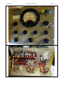
Hickok Model 1890M In-circuit Transistor Tester, S.N. 60947-3.
Original condition is good. Chassis marked 5941 0092.
NSN 6625-00-993-3389. TEST SET, SEMICONDUCTOR DEVICE
NIIN: 00-993-3389
DESIGN CONTROL REFERENCE: 902-353
MANUFACTURERS CODE: 28569
Instruction/service manual is T.O. 33A1-3-206-1 (air force)
Similar unit built under AF contract AF 36(600)-13288. Stock number 6625-731-5716
Meter 50uA
UTC HVC-4 Variductor 0.1H -70/+200%, 30mADC
UTC TF4RX13YY
UTC DO-T11 transistor transformer 10K:2K CT
Industrial transformer corp 3250-84 10Hy 10mA 135Ω DCR
Astron ED-100uF 50V 6418
EKC RN7 resistors
Electrolytic marked 6304
Bourns trimpot
Powering: 14 pins. 5 pins not used.
BT1: Red-J (+), Purple-K (-) = 22.5V (eg. ER763 or Burgess 4156 battery). Red & purple twisted
pair to 100uF 50V can to battery switch S1 (pur to wafer 6; red to wafer 1,2).
BT2: White/yell-C (+0V), White/Orange-B (-3V), Yellow/black-A (-4.5) (eg. ER 761-T or Burgess
2370). 0V yel/blk to battery switch S1 wafer 5. Wh/or to circuit impedance S5 wafer 1. Wh/yel to
battery switch S1 wafer 4.
BT3: White/red-D (+0), Brown-E (-1.5V), Orange-F (-3V), Yellow-H (-4.5V) (eg. ER 761-T or
Burgess 2370). Used for Collector Volts selection circuit. -4.5V yel to collector volts switch S3. 3V or to collector volts switch S3. -1.5V br to collector volts switch S3. +0 yel/rd to collector volts
switch S3 and battery switch S1 wafer 4. Collector volts switch output to battery test S1 wafer 3
(operate to collector EUT terminal).
Some circuitry differences to the Hickok 890.
Defence search:
https://www.logsa.army.mil/etms/
http://www.ebaman.com/index.php/remo...t-Equipment/Hickok/Hickok-890/
Issues:
3 isolated batteries with multiple voltage taps. BT1 uses a 3k3Ω test (7mA, 150mW), and use 1x
LM317L and ~26-30VDC supply. BT2 can use 2x LM317L, and ~7VDC supply. BT3 collector
current supply has 100mA range, so need to use 3x LM317 regs, and ~7VDC supply.
12/05/2015
Hickok 1890M Tester
Page 2 of 3
12/05/2015
Hickok 1890M Tester
Page 3 of 3
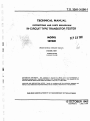
T.0.33A1-3-206 ..1
-
..~.....
TECHNICAL MANUAL
INSTRUCTIONS
AND
PARTS BREAKDOWN
IN-C~RCUITTYPE TRANSISTOR.,. TESTER
."
MODEL
1890M
,
SEP 2.81988
.•.....
(HICICOIC ElKTRICAL
/
10
INSTRUMENT COMPANY)
AF36(600)-13288
'F41608-84.o-A384
~41606-67-D-A28e
DISTFlIBUTION STATEMENT - This .publicationis required fo~ officialuse':or
fot Administr!ltive or
Operational purposes only. Distribution is limited to U.S. Governin~/lt agenc)es,· Other requests for ,this
document shall be referreq to San Antonio ALC/MMEDT. Kelly AFB. TX 7~241-500D,
.,'
HANDLING ANP DESTRUCTION NOTICE -iiandlein
compliance with 'tile distril!lution statement and
de~troy by any method that will prevent disclosure of the cont~ntspr reconstruction of t!le document.
Pt.fBLIIHED
UNDER
AUTHORITY
OF THESECRETARV
OF THE AIR FQRCE
15' OCTOBER
C~NGE
12
1962
1JULY 1988
1":-;
!.:'." ..
T.O.
33Al-3-206-l
INSERT LATEST CHANGED PAGES.
LIST OF EFFECTIVE PAGES
NOTE:
DESTROY SUPERSEDED
PAGES.
The portion of the text affected by the changes is indicated by a
vertical line in the outer margins of the page. Changes to illustrations are indicated by miniature pointing hands. Changes to
wiring diagrams are indicated by shaded areas.
Dates of issue for original and changed pages are:
Original ••• O
lS
Change •..•• l
30
Change .•••• 2 •.• lS
Change ..•.• 3 ..• l5
Change .•••• 4 .... 1
Change ..•.. S ••• 13
Chanqe • .; ••• 6:••• 30
Oct 62
Sep 63
Apr 64
Nov 64
Mar 65
Jun 69
Oct 69
Change
Change
Change
Change
Change
Change
••••. 7..•l5 Oct
••••• 8~..•lSep
••••• 9 •••• l Apr
..•. IO ....l Jul
•... ll •..lS Dec
•.•. 12 •.•• 1 Ju1
TOTAL NUMBER OF PAGES IN THIS PUBLICATION IS
Page
No.
"Change
No.
Page
No.
84
"Change
No.
Title .•......•... 12
39 •....••..•••••••
A•••••••••••.•••.
12
i
S
ii Blank •.•.•••... 5
40 Blank ..•.•.•••• O
1
2 -
74
76
r
t.
82
82
85
88
CONSISTING OF THE FOLLOWING:
Page
No.
0
"Change
No.
f~
[gj
II':Ul,
1
3 •••••••••••••
0
4 Blank ......•.... O
5 - 8 •.••••••••••.
9 .....••••••••••••
0
3
10 - 17....••.•••.0
18 ..•.•..•..••••.
11
19 - 20 •••••••••••
0
21 ••••.•
'••••••••••
~
7
22 - 23 •••••.••.•. 0
24 ..•..•.•.•.•••••
1
25 ..••..••.•••••..
26 ..••......•.....
26A .•..•••••...•..
26B Blank •........
26C .•..•.•.••.••••
26D ....•.•........
26E •••.•••••••••••
4
0
6
6
6
5
8
I
I'--'" ,
r·.···;~'~
u
26F - 26G ••••••••• S
26H ••••••••••••••• 8
26I - 26Z •••••••••
5
26AA - 26AL •••••.• 5
26AM.
• ••••••••
6
26
- 26AZ
Deleted. •• •.... 5
~A - 26BP
Delete¢ ••••.•.• 5
2
•••••••••••
a
38 .........•.....
12
L
* Zero
A
Change
in this column indicates an original page.
12
I
t~_.
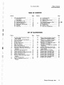
Table of Contents
List of illustrations
T. O. 33AI-3-206-1
TABLE OF CONTENTS
Page
Section
I
I
I
Section
1
USE AND MAINTENANCE
1. Introduction . • . . •
5. Description
• • • • • •
21. Preparation
for Use •
22. Operating Instructions
36. Tester Limitations
..
43. Maintenance Instructions.
45. Cleaning. •
46. Inspection.
. • • . • • • •
1
1
9
9
16
18
18
18
II
Page
47. Troubleshooting.
• • • •
49. Disassembly
•••.••
51. Repair or Replacement.
52. Calibration
. • • . • • ••
••
61A. Transistor Reference Charr • ~. ~ •
PARTS BREAKDOWN.
•
62. Introduction.
. • . . . •
65. Vendor's Code •.•••
67. Reference Designations.
18
18
21
,21
26MB.
27
27
27
27
~:
'~~
LIST OF ILLUSTRATIONS
Figure
1
I
,.;;-,.-
I
,.!,
2
3
4
5
6
7
8
9
10
11
12
13
14
15
16
17
18
Page
In-Circuit Type Transistor
Tester
Model 1890M
Tester Schematic Wiring Diagram
leBO Test Circuit.
•
le Test Circuit
Z Ohms Test Circuit
RIN Test Circuit.
. •
Diode Test Circuit.
•
Battery Wlring Diagram
Operating Controls and Indicators
Functions of Operating COI.1trols and
Indicators
Transistor
Lead Identification
Typical Detector Circuit
Typical Transformer Diode Gate Circuit
Typical Switching Circuit • • • • ••
Schmitt Trigger Circuit.
. • • • • .
Directly Coupled Monostable Multivibrator
Troubleshooting
Chart ..
Table of Switching Circuit D-C
Voltages
...
...
.....
.
....
Figure
2
19
3
6
6
7
8
8
9
10
11
2Q
13
16
17
21
22
23
24
25
26
27
28
17
29
17
18
30
31
32
19
22
33
Page
Table of Audio Oscillator Circuit's .
Voltage and Resistance Values
Table of A. C. Amplifier Circuit's
Voltage and Resistance Values
Calibration Test Equipment.
. • •
Voltmeter D-C Voltages for Audio
Oscillator Transistors
Voltmeter D-C Voltages for Amplifier
Transistors
Amplifier Calibration Test Set Up
In-Circuit Type Transistor
Tester
Model 1890M
Panel and Chassis Assembly
Terminal Board Assembly TB6 .
Terminal Board Assembly TB2 .
Terminal Board Assembly TBI .
Terminal Board Assembly TB5 .
Terminal Board Assembly TB4 •
Terminal Board Assembly TB3 .
Portable Case Assembly .•.•.
..
Changed 15 December 1964
23
23
24
24
24
25
30
31
33
34
35
36
:rr
38
39
i/ii
Section I
Paragraphs 1 to 7
T.O. 33A1-3-206-1
SECTION I
USE AND MAINTENANCE
Transistor
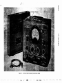
1. INTRODUCTION.
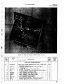
2. SCOPE OF MANUAL. . This technical manual
. covers installation, operation, maintenance andparts
breakdown of In-Circuit Type Transistor Tester
~o~e1-J.B9PM. (figure 1), Federal stock Number
6625~993-3389, hereafter referred to as tester.
The
tester is manufactured by The Hickok' Electrical Instrument Company, Cleveland, Ohio.
I
11
it
I
3. PURPOSE AND FEATURES OF EQUIPMENT.
The tester is designed to test all small and medium power transistors and diodes. directly in or out
of their circuits.
A portable aluminum case. houses
the complete equipment. Access
the control panel
is provided by the detachable top case. in which the
test lead assembly is stored.
to
4. SPECIFICATIONS. Principle features and characteristics of the tester are listed below.
Batteries required •
(not supplied) .
. 1 - 22.5-volt
Eveready
No. 763
2 - 4.5-volt
ST Burgess
No. 2370
Type
Function
Q1, Q2
2N651A
1000 cp.s Oscillator·
Q3
2N650A
A.C. Meter Amplifier 1st Stage
Q4,Q5'
2N651A
A.C. Meter Amplifier 2nd Stage and 3rd Stage
5. DESCRIPTION~
6. GENERAL; Six major circuits are incorporated
in the tester to provide the means to accomplish the
basic tests listed below. Ifhe circuits are briefly
described in paragraphs 7 through 20.
a.
ICBO (collector leakage current):
b.
Ie (collector .cur-rent) .
. c.
I
Meter scales
lCBO Ranges
·0-50 ua,
0-500Ua. and :
complement
Z ohms (external input impedance).
.
.
.
d. RIN (dynamic inptrtimpedance).
e. Beta (current gain of a transistor
emitter configuration).
inthe common
0-5 ma
7.
IC Ranges.
.0-1.0 ma, 0-10 ma and
0-100 ma
Beta Ranges . . . .
.0-50, 0-100, 0-200 and
0-400
Beta Test Accuracy
Meter sensitivity
.....
.....
±
5% for Circuit Impedances above 25 ohms ..
on the 0:"100Beta
.50 ua, 100 mv
AC test signal
Signal
....
.1000 cps sine wave, with
a variable amplitude
Calibration setting
·5 ua Base Current for
the 0-100 Beta Range
Transistor input resistance IWnge
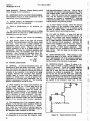
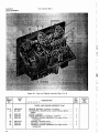
POWERSUPPLY CIRCUIT. (See figure 2).
a. .The tester and its associated circuitry for testing a transistor is energized in the OPERATE position of theBattery
switch 81. The BATT. TEST
position of this switch will be explained in conjunction with the FUNCTIONSELECTOR switch S4 (paragraph 12) because they are interrelated.
The Battery switch is a three-position, momentary contact,
center OFF spring return in both directions - that
is, to the left and right.
The switch always returns
to the center position after it has been released.
. b. The internal power requirements of the audio
oscillator, the A. C. amplifier and meter circuit are
supplied by a 22. 5-volt battery BTl..
c. The collector voltage for the transistor under
test ·is obtained from a tapped 4.5 -volt battery BT3.
. The collector voltage can be varied from 0 to 4. 5·
. volts in 1. 5-volt steps by changing the position of
the COLLECTOR VOLTS switch S3 .
.50-10,000 ohms
Circuit input impedance Range
.25-100,000 ohms
Collector voltages
.0, 1. 5V, 3V, 4.5V
.
d. The collector current can.be varied from 0 - 1
ma, 0 - 10 ma and 0 - 100 ma, depending upon external circuitry conditions, by varying the current
into the base of the transistor under test.
This is
accomplished by using IC potentiometer (R24) across
Changed 30 september
1963
1
.#<\
'l'
iL
'>,
"'"
m
N
it•..
§
w
w
...
>
I
W
I
N
g,
...
Figure 1.
In-Circuit Type Transistor
Tester Model 1890M
T.O. 33Al-3-206-1
the 1. 5-volt tap of battery BT2 when the cmcUIT
IMPEDANCE switch S5 is in the NORMALposition,
and across the 4. 5-volt tap of battery BT2 when the
CmCUIT IMPEDANCE switch S5 is in the LOW position.
This arrangement gives a variable biasing
network for the base to emitter circuit of the transistor under test.
8. AUDIO OSCILLATOR. (See figure 2). A 1000
cps Colpitts Oscillator consisting of a tuned circuit,
transistor
Ql and its associated biasing and feedback networks, is used to generate the A. C. test
signal.
The output of the oscillator is A. C. coupled
into an emitter follower Q2 whose output is then
coupled into the step-down transformer T1 by means
of the BETA CAL potentiometer R8 located in the
emitter circuit of the amplifier.
The output of T1
is connected to the variable resistance bridge (paragraph 9) through the FUNCTION SELECTOR switch
S4. The amplitude of the test signal is controlled
by the BETA CAL potentiometer R8.
9. VARIABLE RESISTANCE BRIOOE
(See figure 2).
I:.;".'
tlfi
CmCUIT.
a. One leg of the bridge circuit is the base to
emitter input impedance of the transistor under test.
This input impedance can be the parallel combination
of the external circuitry impedance of the transistor
under test and its dynamic input resistance.
The
balancing leg is provided by the tester; it consists
of one dual potentiometer Z OHMS CmCUIT (R9 and
R11) and a single potentiometer RIN TRANSISTOR
R10 which is connected in parallel with the dual
potentiometer in the last three positions of the
FUNCTION SELECTOR switch S4. The dual potentiometer is used to null out the external circuit
impedance of the transistor under test.
If an "out
of circuit" test is performed, this dual potentiometer
must be removed from the circuit.
A SPST switch,
which is an integral part of potentiometer R9, is
provided to accomplish this condition. The single
potentiometer (RIN TRANSISTORR10) is used to null
out the dynamic input resistance of the transistor.
b. The functions of the CmCUIT IMPEDANCE
switch 85 are to change the circuit constants in the
bridge and also to change the applied battery voltages to the forward biasing network which is used
to adjust the collector current of the transistor under
test.
In the LOW position, the circuit constants are
given low resistance values in order to present a
low driving impedance to the external circuitry and
transistor
under test.
However, in the NORMAL
position, the circuit constants are given nominal
values, thus presenting a normal driving impedance
to the external circuitry and transistor under test.
The setting of the CIRCUIT INIPEDANCE switch 85
to LOW or NORMAL will depend upon the impedance of the external circuitry and transistor under
Section I
Paragraphs B to 15
RF-IF and audio amplifiers where the external circuitry and transistor impedances areabove 5000hms,
the NORMALposition is selected.
d. When estimating the external circuit impedance
at 1000 cps, only the circuitry between the base and
emitter is considered.
If there is any doubt as to
which position to use, the NORMAL position is selected.
In either position of the CIRCUIT IMPEDANCE
switch, the transistor must be tested below its
maximum collector dissipation.
10. A. C. VOLTMETER CIRCUIT. (See figure 2).
The A. C. voltmeter circuit consists of a three-stage
amplifier (Q3, Q4, Q5) which is highly degenerative
to provide excellent stability, and a crystal diode
bridge detector.
The input sensitivity of the amplifier is 0.5 uv P-P or 0.176 uv RMS for full scale
deflection of the meter.
11. TYPE SELECTOR SWITCH CIRCUIT. (See
figure 2). The TYPE selector switch 82 is a threeposition switch which changes the polarity of the
applied voltages to the transistor or diode under
test.
The three positions of the switch are PNP,
NPN and DIODE. The position of the switch is determined by the circuit element to be tested, that
is, an NPN or PNP transistor, or a diode.
12. TEST CIRCUITS. The various test circuits are
set up by the FUNCTION SELECTOR switch.
Following is an explanation of these circuits.
13. ICBO TEST CIRCUIT. (See figure 3). In the
ICBO test, a reverse voltage is applied across the
collector-base diode of the transistor.
The emitter
is open-circuited.
(The transistor must be removed
from its circuit for this test.]
The collector cutoff
current is read directly on the 0-50 ua scale of the
meter and the appropriate multiplier of the CIRCUIT
IMPEDANCE' switch S5 is used, that is, Xl, X10,
or X100. The meter Ml is connected in series with
a limiting resistor (R17 in this case) to the applied
voltage (battery BT2) and the transistor under test.
14. BATTERY TEST CIRCUlT #1. (See figure 2).
By placing the Battery switch 81 to the BATT. TEST
position, the tester and its associated circuitry is
de-energized and the 22. 5-volt battery BTl is tested
under a fixed load of 3.3K. The quality of the battery is read from the meter scale, which is in two
colors, red and green.
The red portion of the scale
indicates that the battery is low, while the green
portion of the scale indicates that the battery is good.
test.
c. In transistor
power amplifiers where the external circuitry and transistor impedances are normally low or in any circuit where the impedance is
under 500 ohms, the LOW position of CIRCUIT IMPEDANCE switch S5 is selected.
In small signal
15. IC TEST CIRCUIT. (See figure 4).
The IC
control adjustment is made in the following manner
when testing transistors
"in circuit":
The IC potentiometer R24 is set to "zero" or its minimum
position. Note the shunt leakage current on the 0-1. 0
ma scale of the meter and the appropriate multi,5
T.O. 33Al-3-206-1
Section I
Paragraph 16
R22
20.2J\.
\....
--_n
XIOO·
R21
R15
ZZZ.ZJ\.
\ ..•..
---OXIO
47J\.
\J'"'--....(') XIOO
R16
XI
S4
54
470J\.
\ ..•..
--~
XIO
S5
+
,.)-:-~:O---""''''''--''
Ml
(USED AS
MICROAMMETER)
54
Figure 3. ICBO Test Circuit
plier of the Current Range switch S5A and S5B should
be used, that is, Xl, XlO or XlOO. Under these
circumstances the meter is reading the stray leakage current flowing in the external circuitry due to
the collector supply voltage.
The IC potentiometer
is then adjusted for one additional milliampere over
the previously noted reading.
With this setting one
milliampere of collector current will flow through
the transistor which is considered standard for a
small signal beta test.
If a larger collector current
is desired, the IC potentiometer can be adjusted to
the desired value.
16. BATTERY TEST CmCUIT #2. (See figure 2).
When the Battery Switch S1 is placed in the BATT.
TEST position, the quality of the two 4.5-volt batteries BT2 and BT3 is determined by reading the
dual colored scale of the meter.
If the pointer of
the meter is in the red portion of the scale the
batteries are low; if it is in the green portion of
the scale the batteries are good.
~~~A~ji
R31
IJ\.
fro;
f .'
t
I~<
COLLECTOR
VOLTAGE
SUPPLY
54
L2I1
f --~-
R30
10
SlE
6
Figure 4.
IC Test Circuit
T. O. 33Al-3- 206-1
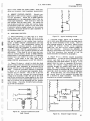
17. Z OHMSCIRCUIT: (See figure 5).
a. To determine the Z ohms circuit input impedance, it is necessary to separate the external
input circuit impedance from the transistor input resistance.
This is accomplished by reversing the bias
on the transistor so that it is cut off, thus separating
the external input circuit impedance from the transistor input resistance.
Paragraphs
Section I
17 to 20
potentiometers R9 and Rll are retained.
The value
of the dynamic input resistance is determined by
varying the RIN TRANSISTORpotentiometer RIO until
a null is indicated on the meter Ml.
The value of
the dynamic input resistance can be read directly
from the calibrated dial of the RIN TRANSISTOR
potentiometer.
c. If the transistor is "out of circuit" the external
input impedance is almost infinite.
Therefore the
Z OHMS CIRCUIT potentiometers must be removed
from the bridge circuit.
This is accomplished with
a SPST switch (an integral part of R9) which is
ganged to the shaft of the small knob of the Z OHMS
CIRCUIT potentiometer. This switch must be placed
to the OUT OF CIRCUIT position to remove the Z
OHMS CIRCUIT potentiometers from the bridge circuit.
19. BETA CAL ANDBETA READ CIRCUITS. Circuits set up by the BETA CAL and BETA READ
positions of FUNCTION SELECTOR switch S4 are
the same as that shown in figure 6, except for location of the meter Ml.
Beta is the current gain
of a transistor in the common emitter configuration
which is the ratio of the a-c collector current to
the a-c base current.
To measure both of these
currents, a monitoring resistor of 49. 9 ohms (R12)
is placed in the bridge circuit and another monitoring
resistor of 1 ohm (R3l) in the collector circuit.
The meter Ml monitors the voltage drops across
these resistors and the AC Beta can be determined.
Placing the FUNCTION SELECTOR switch S4 to the
BETA CAL position, meter Ml monitors the voltage drop across the 49.9-ohm resistor; the BETA
CAL potentiometer R8 is adjusted until the meter
reads- 1/2 scale or CAL SET. Under this condition
there is 5 ua of current flowing in the base circuit.
The FUNCTION SELECTOR switch is then placed to
the BETA position.
This switches the meter across
the I-ohm monitoring resistor and the meter reads
AC Beta directly.
18. RINTRANSISTOR CIRCUIT. (See figure 6). The
dynamic input resistance of the transistor
is determined by using the same technique used in determining the external input circuit impedance (paragraph 17). However, in this test the transistor is
biased in the forward direction, and the previous
settings (paragraph 17) of the Z OHMS CIRCUIT
20. DIODE TEST CmCUIT.
(See figure 7). The
circuitry used to perform the diode tests is essentially the same as that used for the transistor tests.
The only difference between the circuitry is the
functions performed by the TYPE selector switch 82.
This switch performs three different functions, the
first of which is to reverse the meter Ml in the IC
b. The external input circuit impedance forms one
leg of the bridge circuit and its value is determined
by varying the Z OHMS CIRCUIT potentiometers R9
and Rll until a null is indicated on the sensitive a-c
voltmeter tied across the bridge.
The value of this
external input circuit impedance can be read directly
from the calibrated dials of the Z OHMS CIRCUIT
potentiometers.
This null must be made very carefully because it can affect the next test, which is
the RIN of the transistor.
T1
COLLECTOR
VOLTAGE
BETA~II
SUPPLY
eAl
R8
l211
SlC
R24
MI
(USED AS A-C
VOLTMETER)
IcADJ•
SlE
R30
10
S4H
Figure 5.
Z Ohms Test Circuit
7
T.O. 33Al-3-206-1
Section I
!
--,':
L
Tlll
BETA
CAL
RS
COLLECTOR
VOLTAGE
SUPPLY
~
l21
R30
10
SlE
Figure 6. RIN Test Circuit
position of the FUNCTION SELECTOR switch S4, so
that the total current drawn by the diode and its external circuitry can be measured. Secondly it shorts
out the current limiting resistors (R21 and R22) in
the collector circuit, which are used to protect the
meter if a shorted transistor is tested and lastly it
removes the collector voltage supply in the last 5
posttrons ofthe FUNCTIONSELECTOR switch. Compare figure 7 with figure 4 and note the differences.
R31
I~
~OUTOF
CIRCUIT
R9
500
B
DIODE
UNDER
TEST
r
I,.R30
I·
10
i
1_-
SlE
Figure 7. Diode Test Circuit
8
f
l._.
T.O. 33Al-3-206-1
Paragraphs
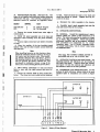
21. PREPARATION FOR USE. (See figure 8). The
tester is not supplied with batteries because batteries
deteriorate with age. The following complement of
batteries should be installed as explained below.
to lugs.
Figure 8 shows the color of the leads and
where they should be placed.
Tighten each lug securely to its stud.
g.
Symbol
Section I
21 to 25
Reconnect the cable assembly to the chassis.
Quantity
BT2 and BT3
BTI
2
1
h. Carefully insert panel assembly back into the
case and secure with the ten screws.
No. 2370 ST Burgess
No. 763 Eveready
22. OPERATING INSTRUCTIONS.
a. Remove ten screws located near outer edge. of
control panel.
•
'
•.'
....
.
I
23. GENERAL. Consult the manufacturer's specification sheets for values of the transistors to be
tested. The tests performed by the tester are rcso,
IC, Z ohms, Rm, and BETA. These tests must be
performed carefully and in the sequence indicated.
Test procedures are categorized by "in circuit"
transistor
tests, "out of circuit" transistor tests,
"in circuit" diode tests, "out of circuit" diode tests,
and additonal tests .
b. Gebtiy lift panel assembly out of its case and
disconnect cable assembly from the panel assembly
chassis.
c. Remove eight screws that hold battery brackets
to case.
d. Place the smaller of the two brackets around
battery BTI and the other bracket around batteries
BT2 and BT3.
Note
Note
When installing batteries in their brackets, there
.should be sufficient clearance between the lip of
the bracket and the battery studs. When installing Military Batteries BA-2 and BA-27, reverse
the mounting brackets so that the bracket flanges
will be opposite the battery terminal end. Use
pressboard or cardboard to insure a snug fit for
battery BT-1 when installing Military Battery BA-2.
The leBO test (collector leakage current) is
performed only as an "out of circuit" test.
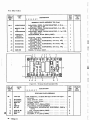
24. OPERATING CONTROLS AND INDICATORS.
The
operating' controls and indicators are all located on
the front of the tester.
Figure 9 shows the location
and figure 10 lists the controls and indicators and
the function of each one of their positions.
e. Place battery assemblies in case and secure
them to case with the eight screws that were removed.
f. Connect the various leads to their proper -batteries.
The wires are color-coded and are soldered
25. TRANSISTORLEAD IDENTIFICATION. For the
purpose of quick reference, bottom views of the most
common types of transistors
are shown in f~re
11.
BATTERY B2
-4.S
---
BATTERY
srt
..,-
-3
-L5
C?
0
+
e
BATIERY 813
-~
-
-
+~2.5
-3
9
Y
+
4)
I
·z
..,~. .
oli
elL
alo
•••
~
''':
.J%
.,:
•
%
~:. :.
0
•••
II:
. . z •.
~~lI:i
>011I
I
I
I I I
A B
C
H FED
I
I I
( J K
I
..i
xII::
Figure 8.
I
)
Jl
Battery Wiring Diagram
Changed 15 November 1964
9
Section I
paragraphs 26 to 27
T.O. 33Al-3-206-1
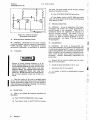
Figure 9. Ope~ting, Controls and Indicators.
26. PRELIMINARYADJUSTMENTSANDCONTROL
SETTINGS. Before attempting to test. any transistor
or diode do the following.
27. "IN CmCUIT" TRANSISTORTESTS. The test
procedure for the "in circuit" transistor test is as
follows.
a. 'Place FuNCTIoN SELECTORswitch to leBO.
Rotate Battery switch to BATT. TEST andimonftorthe meter; meter should 'read on green. portion
a. 'Connectthe three colored banana plugs ofthe test '
lead assembly to their respective binding posts (E,
B and C) located on the tester control panel. Then
connect the other' end of the test leads to transistor
to be tested. The,yellow lead is connected to emitter,
green lead to base and blue lead to collector.
(GOOD).
b.:place FUNCTIONSELECTORswitch to IC:. notate Batt~ry switch to BATT. TEST and monitor the
meter; meteJ.:,~hould r~ad on green portion (GOOD).
c.Rotate the IC and BETA tAL potentiometers
to their mimmum positions.
b. Set the TYPE selector switch to either the PNP
or NPN position, dependingupon which type of transistor is to be tested.
'
c. Turn IC and BETA CAL potentiometers to
"zero", or minimum, postttons,
.,
If the IC and' BETA CAL potentiometers are
not set at their minimum positions, possible
damage could be incurred to the transistor or
diode to be tested.
d. Using a screwdriver on the Zero Adjustment,
zero the meter.
10
d. Set CmCUlT IMPEDANCEswitch' to NORMAL
circuit impedance is above 500 ohms or to LOW
if circuit impedance is below 500 ohms.
if
e. Set the ,COLLECTORVOLTS switch to the
collector voltage desired for testmg. the transistor
(1.5, 3, ~. 5).
Section I
T.O. 33AI-3-206-1
CONTROL or INDICATOR
POSITION
or SCALE-
FUNCTION
Battery switch SI
OPERATE
Energizes tester circuitry for
testing a transistor.
BATT. _TEST
With FUNCTION SELECTOR switch
84 in position 1 (ICBO), the tester
and its associated circuitry is deenergized and the 22. 5-volt battery BTI
is tested under a fixed load of 3. 3K.
With FUNCTION SELECTOR switch
84 in position 2 (IC), the two 4. 5-volt
batteries BT2 and BT3 are tested.
TYPE selector
switch S2
OFF
De-energizes
PNP
Sets the correct polarity of the applied
voltages to the PNP transistor under
test.
NPN
Sets the correct polarity of the applied
voltages to the NPN transistor under
test.
DIODE
With FUNCTION SELECTOR switch 54
at Ie, meter Ml is reversed.
I.·
II
the tester.
Shorts out current limiting resistors
R14, R15 and R16.
Removes collector voltage supply in
positions 2 to 6 of FUNCTION SELECTOR
switch 84.
COLLECTOR VOLTS switch S3
FUNCTION SELECTOR switch 84
0
De-energizes the 4. 5-volt battery BT3
potential to the collector of the transistor
under test.
1. 5, 3,4.5
Applies voltage to collector of the
transistor from battery BTS in 1. 5-volt
steps.
1 - leBO
With the Battery switch 81 to BATT.
TEST position, the tester and its
associated circuitry is de-energized
and the 22. 5-volt battery BTI is tested
under a fixed load of 3. 3K.
In the leBO test (Battery switch 81 in
OPERATE position), a reverse voltage
Is applied acrose the collector-base
diode and the emitter is open-circuited
in this test. Meter Ml and the appropriate limiting resistor are placed in
series with the circuit.
2 - Ie
With the Battery switch 81 to BATT.
TE8T position, the two 4. 5-volt
batteries BT2 and BT3 are tested.
Figure 10. Functions of Operating Controls and Indicators
(Sheet 1 of 3)
11
T.O. 33Al-3-206-1
Section I
CONTROL or INDICATOR
POSITION
or SCALE
FUNCTION
In the Ie test (Battery switch Sl in
OPERA TE position), the Ie potentiometer
R24 is energized, meter M1 and
appropriate limiting resistor are switched
into the collector circuit and the variable
resistance bridge into the circuit.
3 - Z OHMS
CmCUIT
Reverses bias on the transistor under
test and switches meter M1 across the
bridge circuit.
4 - RrnOHMS
TRANSISTOR
Switches Rrn OHMS TRANSISTOR potentiometer R10 into the bridge circuit.
Forward biases on the transistor under
test and retains meter M1 across the
bridge.
5 - BETA
CAL
Places meter M1 across monitoring
resistor R12 (49.9 ohms) in the bridge
circuit.
6 - BETA
READ
Places meter M1 across monitoring
resistor RS1 (1 ohm) in the collector
circuit for a Beta reading on meter Ml.
LOW
Places Ie potentiometer R24 across
4. 5-volt tap of battery BT2.
I·····
CIRCUIT IMPEDANCE
switch S5C and S5D
the
Switches the two 10-ohm resistors (R28
and RSO) into the bridge circuit and
shorts out resistor Rll.
NORMAL
Places Ie potentiometer R24 across
1. 5-volt tap of battery BT2.
Places resistors
bridge circuit.
CURRENT RANGE
switch S5A and S5B
xi, X10,
X100
R24
Z OHMS CIRCUIT
potentiometers R9 and
Rll
---
Any position
except OUT
OF
CIRCUIT
L.
' -,
, <,J
fC.....:
the
R27 and R29 into the
Connects the appropriate meter shunt
resistor into the circuit which determines
the multiplier used when reading meter
Ml.
Inserts a limiting resistor
with the meter.
IC potentiometer
j
in series
With the FUNCTION SELECTOR switch
S4 in position 2, the Ie potentiometer R24
is used to adjust collector current flow
of the transistor under test.
With the FUNCTION SELECTOR switch
S4 in position 3, the Z OHMS CIRCUIT
potentiometers are adjusted to provide
the balancing leg of the bridge circuit.
It also provides direct reading of the
external input impedance.
I'
I'---
\
I
t.·~
Figure 10.
12
Functions of Operating Controls and Indicators
(Sheet 2 of 3)
T.O. 33A1-3-206-1
CONTROL or INDICATOR
I
Section I
POSITION
or SCALE
FUNCTION
OUT OF
CmCUlT
Removes Z OHMSCIRCUIT potentiometers
R9 and Rll from the bridge circuit
during "out of circuit" transistor tests.
RIN TRANSISTOR
potentiometer R10
---
With the FUNCTION SELECTOR switch
S4 in position 4, the RIN TRANSISTOR
potentiometer is used to balance the
bridge circuit and provide direct reading
of the dynamic input resistance of the
transistor under test.
BETA CAL
potentiometer
---
R8
Meter M1
With the FUNCTION SELECTOR switch
S4 in posttlon 5, the BETA CAL potentiometer R8 is used to adjust meter
Ml to read CAL SET permitting 5 ua
of current to flow in the base circuit
of the transistor under test.
BATTERY
LOW-GOOD
With the Battery switch Sl at BATT.
TEST and the FUNCTION SELECTOR
switch S4 in position 1, condition of
battery BT1 is indicated.
With the Battery switch S1 at BATT.
TEST and the FUNCTION SELECTOR
switch S4 in position 2, condition of the
two 4. 5-volt batteries BT2 and BT3
is indicated.
Ie 0-1 MA.
Indicates collector current flow when the
potentiometer R24 is used to forward
bias the transistor under test.
ICBO
0-50 UA.
Indicates Beta of transistor under test
for full scale calibration of the meter.
0-100
Indicates Beta of transistor under test
for 1/2, 1/4 and 1/8 scale calibration
of the meter.
Binding Posts
El, E2, E3
E,B,C
Connects to respectively colored banana
plugs of lead assembly for "in circuit"
transistor tests.
Socket J2
---
Zero ADJUSTMENT
---
I
Figure 10.
!-c
Provides connection to transistor
"out of circuit" tests.
for
Used to "zero" meter Ml.
Functions of Operating Controls and Indicators
(Sheet 3 of 3)
TRANSISTOR
HOUSING
RED DOT
0
~
EB e
EBe
Figure 11. Transistor
eBE
e
Lead Identification
13
Section I
Paragraphs 28 to 29
T.O. 33Al-3-206-1
f. Place FUNCTIONSELECTORswitch to Ie position and Current Range switch to XIO. Turn Bat.•
tery switch to OPERATE. This energizes the tester.
g. Observe the shunt leakage current on the 0-1
MA. scale of the meter and apply its proper multiplier (XIO in this case) to determine current flow.
Under these circumstances the meter is reading the stray leakage current flowing in the external circuitry due to the collector supply
voltage.
h. Adjust the collector current with IC potentiometer for one additional milliampere over the
previously noted reading. If the stray leakage CUrrent is high (3, 4 or 5 MA), set collector current
to at least twice the noted stray leakage current,
by adjusting Ie potentiometer.
Power type transistors, used in the final
audio output stages of transistor radios, should
be checkedwith 5 or 10 MA. of collector current.
. switch to the BETA READand read Beta directly on
the meter. If the Beta of the transistor is higher
than 100, recalibrate meter to 1/4 scale and multiply meter reading by 2. If Beta of the transistor
is higher than 200, recalibrate meter to 1/8 scale
and multiply meter reading by 4. If the beta of the
transistor is below 50, and an accurate value of
Beta is required, recalibrate meter to full scale
and read Beta directly on 0-50 scale of meter.
28. ''OUTOF CIRCUIT"TRANSISTOR
TESTS. The
test procedure for the "out of circuit" test condition
is almost identical to that of the "in circuit" test
procedure. The only difference is that the ICBOtest
is performed and the Z Ohms test is omitted. When
omitting the Z Ohms test, the Z OHMSCIRCurr
potentiometer must be switchedto the OUT OF CIRCUIT poSition. The test procedure for the "out of
Circuit" transistor test is as follows.
a. Remove transistor which is to be tested from
its circuit. Either plug it into socket located on
control panel (identified as EB C) or perform step
a of paragraph 27.
b. Switch Z OHMSCmCUIT potentiometer to OUT
OF CIRCUITposition.
c. Perform steps b through e, paragraph 27.
d. Place FUNCTIONSELECTOR switch to leBO
and Current Range switch to Xloo.
Do not change current multipliers while the
tester is energized.
i. Rotate the VERNIER of the Z OHMSpotentiometer to approximately 250 ohms, or mid position.
j. Place FUNCTIONSELECTOR switch to the Z
OHMSCIRCUITposition and turn the Battery switch
to the right.
k. Increase amplitude of audio oscillator by turning
BETA CALpotentiometer until meter reads approximately half scale. Balance the bridge by first varying
the large control of Z OHMSCIRCUITpotentiometer
to obtain an approximate null; adjust VERNIERto
obtain a precise null as indicated on meter. Value
of external input impedance can nowbe read directly
from the calibrated dials of Z OHMSCIRCUITpotentiometers.
1. Place FUNCTION SELECTOR switch to RIN
TRANSISTOR;turn Battery switch to the right and
increase amplitude of audio oscillator. Adjust RIN
TRANSISTORpotentiometer to balance the bridge
circuit. A null will be indicated on the meter when
the bridge' is balanced. The value of the dynamic
input resistance of the transistor is read directly
from the calibrated dial of the RIN TRANSISTOR
potentiometer.
m. Place FUNCTIONSELECTORswitch to BETA
CAL. Turn Battery switch to the right and adjust
BETA CALpotentiometer until meter reads 1/2 scale
or CAL SET. Then place FUNCTIONSELECTOR
14
e. Turn Battery switch to the right and monitor
the leBO scale of the meter for leakage current.
If current reading is low, release Battery switch
and place Current Range switch to XIO or Xl, dependingupon what current is measured.
f. Perform steps f, g, h, 1, and m, paragraph
27.
29. ''IN CIRCUIT" DIODE TESTS. Perform the
following procedure for the "in circuit" diode test.
a. Connect the three colored banana plugs of the
test lead assembly to their respective colored binding
posts (E, B and C) on the tester. Then connect
the other end of the test leads to the diode to be
tested. The green lead is connected to cathode end,
. blue lead to anode and the yellow lead is left opencircuited.
b. Set the TYPE selector switch to DIODEand set
the IC and BETA CAL potentiometers to their minimum positions.
c. Place CIRCUITIMPEDANCEswitch to LOWor
NORMAL,dependingoncircuit impedance;set Current
Range switch to Xl0.
The setting of the COLLECTORVOLTS switch
is immaterial in this test because this supply
is not used in an "in circuit" diode test.
i
T.O. 33Al-3-206-1
Paragraphs
..I '·····'
·~
-:-'{£
{]
d. Place the FUNCTION SELECTOR switch to
IC, and turn Battery switch to the right, energizing
the tester.
e. Adjust IC potentiometer until the meter reads
o. 1 MA. Under this condition the meter is actually
reading 1 MA.
f. Turn FUNCTION SELECTOR switch to Z OHMS
CIRCUIT and increase the amplitude of the audio oscillator by turning BET A CAL potentiometer until
meter reads half scale.
Then vary the Z'OHMS
CIRCUIT potentiometers
until null is obtained on
the meter.
Read the value of external impedance
from calibrated dial of the Z OHMS CIRCUIT potentiometers.
If null occurs near zero or some low
value, the diode can be assumed to be shorted or
leaky.
I
I
g. Place the FUNCTION SELECTOR switch to Rrn
TRANSISTOR and increase amplitude of the audio
oscillator until meter reads half scale.
Then balance the bridge by varying Rrn TRANSISTOR potentiometer
until· null is indicated on the meter.
Read the value of the diode's dynamic forward resistance from the dial of the RIN TRANSISTOR
potentiometer.
Normal values of 50-500 ohms can
be expected.
If a high value of resistance is obtained, the diode can be assumed to be open circuited or the external circuitry which shunts the
diode is extremely low. If the external circuitry
is low, adjust the IC potentiometer until the meter
reads 2 to 5 MA. and then null the diode's dynamic
resistance.
Variations in the dynamic forward resistance of a diode is a function of the d-e current
flowing through the diode.
30. "OUT OF CIRCUIT" DIODE TESTS. The test
porcedure for the "out of circuit" diode test is as
follows.
a. Connect the three colored banana plugs of the
test lead assembly to their respective colored binding
posts (E, B and C) on the tester.
Then connect
the other end of the test leads to the diode to be
tested. The green lead is connected to the cathode
end, blue lead to anode and the yellow lead is left
open-circuited.
b. Set the TYPE selector switch to DIODE and set
the IC and BET A CAL potentiometers to their minimum positions.
c. Place CIRCUIT IMPEDANCE switch to NORMAL
and Current Range switch to XIO.
d.
Set COLLECTOR VOLTS switch to 1. 5.
e. Place FUNCTION SELECTOR switch to lCBO
and turn Battery switch to the right.
Now read the
leakage current of the diode on the meter; then release the Battery switch.
If the meter reading is
high the diode is shorted or very leaky.
f. Place FlJNCTION SELECTOR switch to IC and
turn Battery switch to the right.
Adjust the IC potentiometer until the meter reads O.1 MA. Under
this
Section I
30 to 34
condition the meter is actually reading 1 MA.
g. Place Z OHMS CIRCUIT potentiometers
OUT OF CIRCUIT position.
to their
.
h. Place FUNCTION SELECTOR switch to Rrn
TRANSISTOR and turn Battery switch to the right
Increase the amplitude' of the audio oscillator by
varying the BETA CAL potentiometer until the meter
reads half scale. Then balance the bridge by varying
the Rrn TRANSISTOR potentiometer until null is indicated on the mete r. The value of the diode's dynamic forward resistance is read from the dial of
the RIN TRANSISTOR potentiometer.
31.
ADDITIONALTESTS.
32. GENERAL. The tester is also capable of performing certain other less common tests.
Procedures for these additional tests are explained be.
low.
.
33. "OUT OF CIRCUIT" ICEO TEST FOR SMALL
SIGNAL TYPES.
ICEO is the collector leakage
current with the collector reverse-biased
and the
base open-circuited.
In general the ICEO leakage
current is considerably larger than lCBO. The test
is performed in the following manner.
a. Place TYPE selector switch to either NPN or
PNP, depending upon the type of transistor.
b.
Place COLLECTOR VOLTS switch to 1. 5.
c.
Place
FUNCTION SELECTOR switch to ICBO.
d. Connect collector to the blue lead and emitter
to green lead of lead assembly and leave the base
open -circuited.
e. Place the Current Range Switch to XlOO and
then turn Battery switch to the right.
Read the
leakage current on the 0-50 ua scale of the meter.
If reading is low, place the CUrrent Range switch to
XlO or Xl, depending upon how much leakage current
is being measured.
34. "OUT OF CIRCUIT" lEBO TEST FOR SMALL
SIGNAL TYPES. lEBO is the emitter leakage current with reverse-bias applied to the emitter and the
collector open circuited.
The test is as follows.
a.
Place
TYPE selector
switch to NPN or PNP.
b.
PlaceCOLi..ECTOR VOLTS switch to 1. 5.
c.
Place
FUNCTION SELECTOR switch to ICBO;
d.' Connect base to the green lead, emitter to blue
lead of the lead assembly; the collector is left opencircuited.
e. Place Current Range switch to XlOOand then
turn Battery switch to the right.
Read the leakage
current on the 0-50 ua scale of the meter.
If the
reading is low, place Current Range switch to Xl0
or Xl, depending upon how much leakage current is
15
Section I
ParagIC\phs 35 to 40
T.O. 33Al-3-206-1
being measured.
However, release
when changing current multipliers.
Battery switch
35. IMPEDANCE RATIO OF AUDIOTRANSFORMER.
The impedance ratio of an audio transformer
dete rmtned in the following manner.'
. a. Connect primary of transformer
and green leads of the lead assembly.
; b. Place
~ition.
IC potentiometer
to
its
can be
to the yellow
minimum
po-
: c. Place FUNCTIONSELECTOR switch to Z OHMS
CIRCUIT and be sure that the Z OHMS CIRCUIT potentiometers are in the circuit.
d.
Place
a resistive
load across
the secondary.
e. TuJ:"nBattery switch to the right and increase
the BETA CAL potentiometer until the meter reads
full scale.
Then vary the Z OHMS CIRCUIT potentiometers until null is indicated on the meter.
Release the Battery switch.
Read the value of reflected impedance on dial of Z OHMS CIRCUIT potentiometer.
Knowing the reflected impedance and
the secondary load, the impedance ratio can be determined.
Also, knowing the impedance ratio, the
turns ratio can also be determined.
The turns ratio
is the square root of the impedance ratio.
The
formula is as follows:
TR =\
rz;
Vii-
test when performing a Z ohm test.
This. is due to
extremely low values of self-biasing networks. When
this condition exists, reduce the collector voltage to
zero.
This will reverse bias the transistor under
test, and the external circuitry impedance can be
measured as outlined in paragraph 27. After the
Z Ohm test has been made, return the COLLECTOR
VOLTS switch to its previous position.
d. In some special circuits, where the external
input circuitry of the transistor being tested exhibits a large capacitance (0.5 uf or larger) across
its base to emitter leads, disconnect one side of
this capacitor before performing the tests.
38. R-F AND I-F STAGE. In some R-F and I-F
AVC stages, which have both the base and the low
side of the collector tank heavily bypassed, it is
possible, even under these adverse conditions that
the Z OHM CIRCUIT potentiometers can still null
out the external circuit impedance. However, the
value of this impedance will be very low, almost a
short .crrcuit,
When these circumstances
exist,
open one side of these bypass capacitors.
This
will remove the low impedance from the emitterbase circuit.
Then the stage can be tested in the
usual manner.
39. AUDIODRIVER STAGE. When testing an audio
ouput driver stage of a radio, set the volume control to approximately 1/2 of its maximum resistance.
This will eliminate an a-c short between the base
and the emitter of the transistor being tested.
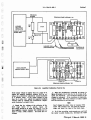
36. TESTER LIMITATIONS.
37. GENERAL. As with all instruments, there are
limitations to which this tester can be used.
Therefore, this section will help the user of the tester to
overcome some of its pitfalls by altering the external
circuitry of the transistor to be tested or by using
a slightly different test procedure when required.
VlLrious .types of circuits with their specifiC difficulties in testing them, as well as special techniques used to overcome these difficulties, are explained in paragraphs 38 through 42. The following
general considerations should be noted.
40. DETECTOR STAGE. Figure 12 shows a detector stage in which a slightly different test procedure is required.
Place the Z OHMS CIRCUIT
potentiometer to the OUT OF CIRCUIT position,
omit the Z Ohm test and then proceed to test the
transistor as outlined in paragraph 27. From figure 12 one can see that the diode isn't conducting
when the transistor is forward biased by the tester.
Therefore the Z Ohm test should be omitted because
the Z Ohm test reverses the forward biasing voltage applied to the transistor under test,
In this
a. While following the regular test procedure for
an "in circuit" test on a circuit which has a low
external input impedance, it is possible that the
transistor
input resistance cannot be nulled out.
Under these circumstances,
it is necessary to increase the collector current of the transistor under
test to decrease its input resistance.
The limitations to the above solution are the collector dissipation of the transistor under test and the shunting
~ffects of the external input ch'cuitry impedance.
b. The maximum ratio of the transistor input resistance to the external input impedance which can
be detected by the bridge circuit is 10 to 1. Therefore, under the lowest limit of external input impedance (25 ohms), the maximum detectable value of
the transistor input resistance is 250 ohms.
_.
c. There are external circuit conditions under which
it is impossible to reverse bias the transistor under
16
Figure 12. Typical Detector Circuit
T.O. 33Al-3-206-1
Section I
Paragraphs 41 to 42
case it also makes the diode conduct, which produces an erroneous input impedance measurement.
B+
B-
41. DIRECT COUPLED CmCUIT.
Directly coupled PNP to NPN circuits require a slightly different test procedure.
Preset the Z OHMS CIRCUIT
potentiometers to the approximate value of the external input impedance. Then omit the Z Ohm test
and continue with the other tests.
The reason for
this deviation is that the Z Ohm test reverse biases
the transistor under test, however at the same time
it acts as a collector supply voltage for the previous
transistor, which then shunts the input impedance of
the transistor under test.
42. SWITCHINGCIRCUITS.
a. When performing a Z Ohm test on a transformer diode gate circuit (figure 13) or on a circuit which uses a diode to limit the reverse bias
that can be applied to the emitter base junction,
preset Z OHMS CIRCUIT potentiometers and omit
the Z Ohm test.
The potentiometer setting will
depend upon the circuitry involved. If the diode is
conducting when the transistor is forward biased,
set the Z OHMS CIRCUIT potentiometers to the
approximate value of the impedance between the base
and emitter.
If the diode is cut off when the transistor is forward biased, set the Z OHMS CIRCUIT
potentiometer to the approximate value of impedance
between base and emitter (in some cases an open
circuit).
If the latter is the case, place the Z
OHMS CIRCUIT potentiometer to OUT OF CIRCUIT.
I
b. Figure 14 shows a circuit in which the diode
doesn't conduct when the transistor is forward biased;
the external input impedance is determined by its
biasing network and the impedance of the previous
stage.
Follow the procedure outlined in paragraph
a, above, or an erroneous input impedance measurement will be obtained. This is due to the fact
that the Z Ohm test reverses the forward biasing
voltage of the transistor under test and at the same
time it also reverses the voltage applied to the diode
in the external circuitry which might cause it to conduct or to become cut off depending upon the polarity
of the voltage.
Check the circuitry before attempting to test the transistor.
Figure 14. Typical Switching Circuit
c. A Schmitt trigger (figure 15) is another circuit in which some difficulties may arise when checking the second transistor of the circuit.
The forward biasing network of the tester, which is used
to adjust the collector current of the transistor
under test, can also act as a collector supply for
the first transistor.
Eliminate this difficulty by
placing a short between the collector and the emitter
of the first transistor; then proceed to test the
second transistor as outlined in paragraph a.
d. Figure 16 is a directly coupled monostable
multivibrator.
To test the three transistors of the
circuit, open lead A for all of the tests and test
transistor Q3 in the usual manner. If lead A is not
opened when the tests on transistor Q3 are performed, the collector voltage supply will be short
circuited through the emitter base diode of transistor Q2. When testing transistor Ql, short the
emitter and base of transistor Q2; when testing transistor Q2, short the emitter and base of transistor
Q1. If this isn't done, one could mistake the leakage current ICEO of the transistor not under test
for a shorted or leaky transistor.
Then test the
transistors as outlined in paragraph a.
B-
1st.
TRANSISTOR
B-
VE
Figure 13. Typical Transformer Diode
Gate Circuit
Figure 15. Schmitt Trigger Circuit
17
Section I
Paragraphs
T. O. 33Al-3-206-1
43 to 50
the meter. The meter should read in the green (GOOD)
portion of the battery test scale.
(3) Place FUNCTION SELECTOR switch to IC.
(4) Turn Battery switch to BAIT. TEST and monitor
meter. The meter should read in the green (GOOD) portion
of the battery test scale.
47.
LEAD A
Figure 16. Directly Coupled
Monostable Multivibrator
43.
MAINTENANCE
INSTRUCTIONS.
44. GENERAL.
Maintenance of the tester consists
of periodic cleaning, periodic inspection, disassembly,
trouble
shooting,
repair
or replacement
of parts,
and periodic calibration.
No lubrication
is required.
45.
CLEANING.
I WARNING
I
Perform all solvent cleaning operations in an approved cleaning cabinet or in a well ventilated area.
Avoid prolonged breathing of vapors. Avoid eye and
repeated skin contact.
Keep solvents away from
sparks and flames. Use approved personal protective
equipment (goggles/face shield) when using compressed air. Provide protection from flying particles.
Do not direct airstream towards self or other personnel.
a. Clean the exterior of the tester as required, using 3
lint-free cloth soaked with cleaning solvent conforming to
Federal Specification P-D-6BO, Type II. Exercise catuion to
avoid removing any identification markings. Dry with compressed air at not more than 30 psi.
I
46.
INSPECTION.
a. Prior to use, perform the inspection procedure outlined below.
(1) Place FUNCTION SELECTOR switch to ICBO.
(2) Turn Battery switch to BATT. TEST and monitor
18
Change 11
TROUBLE SHOOTING.
48. GENERAL.
Incase of malfunction of the tester,
investigate
and remedy the trouble immediately
to
prevent damage to the equipment.
Under no circumstances
should the equipment be operated if it
does not function properly.
See figure 17 for indication of trouble,
probable causes,
and remedial
action to be taken to restore equipment to the required standards.
See figure 2 for the schematic
wiring diagram.
49.
DISASSEMBLY.
50. GENERAL.
The tester
is disassembled
only
to the extent necessary for inspection (paragraph 46),
troubleshooting
(paragraph 47), repair or replacement
of parts (paragraph 51), and calibration (paragraph 52).
Refer to section II of this manual for the parts breakdown, which includes parts location and parts descriptions.
General
disassembly
instructions
are
given below.
a. Remove the ten screws
edge of the control panel.
b.
Gently lift panel assembly
c.
Disconnect
d. To remove
as follows:
located
near
the outer
out of its case.
jack Jl from plug P1.
a switch
or potentiometer
proceed
T. O. 33AI-3-206-1
PROBABLE
CAUSE
TROUBLE
V
Section I
No deflection of meter when
all batteries are tested.
No deflection of meter when 22. 5volt battery BTI is tested.
I
All three batteries
completely dead
Meter deflects to the extreme
right when 22. 5-volt battery
BTI is tested.
are
Replace defective
batteries.
Open circuit
Check continuity and
repair defective
wiring.
Shorted crystal CRI
Replace defective
crystal.
Defective meter Ml
Replace meter.
Defective Battery
switch SI
Replace defective
switch.
Defective FUNCTION
SELECTOR switch 84
Replace defective
switch.
Dead battery BTl
Replace defective
battery.
Shorted capacitor C6
Replace defective
capacitor.
Open circuit
Check continuity and
repair defective
wiring.
Defective Battery
switch SI
Replace defective
switch.
Defective FUNCTION
SELECTOR switch S4
Replace defective
switch.
Shorted resistor
Replace defective
resistor.
Open resistor
No deflection of meter when the
two 4. 5-volt batteries BT2 and
BT3 are tested.
REMEDIAL
ACTION
R25
R26
Replace resistor.
Both batteries are
completely dead
Replace defective
batteries.
Open circuit
Check continuity and
repair defective
wiring.
Defective Battery
switch SI
Replace defective
switch.
Defective FUNCTION
SELECTOR switch S4
Replace defective
switch.
Open resistor
R32
Replace defective
resistor.
Open resistor
R26 shorted
R25 or
Replace defective
resistor.
Figure 17. Troubleshooting
Chart (Sheet 1 of 3)
19
T. O. 33A1-3-206-1
secnon I
REMEDIAL
ACTION
PROBABLE
. CAUSE
TROUBLE
Shorted resistor
No power, or defective power
to audio oscillator.
Defective battery BT1
Replace defective
battery.
Open circuit
Check continuity
and repair defective
wiring.
Defective Battery
switch 81
Replace defective
switch.
Defective battery BT1
Replace defective
battery.
No power, or defective power
to A. C. amplifier.
R32
Open circuit
No power, or defective
collector voltage.
Defective base current.
Figure 17.
20
Replace defective
resistor.
Meter deflects to the extreme
right when the two 4. 5-volt
batteries BT2 and BT3 are
tested.
Check continuity and
repair defective
wiring.
Defective Battery
switch S1
Replace defective
switch.
Defective battery BT3
Replace defective
battery
Open circuit
Check continuity and
repair defective
wiring.
Defective COLLECTOR
VOLTS switch S3
Replace defective
switch.
Defective Battery
switch 81
Replace defective
switch.
Defective TYPE
selector switch S2
Replace defective
switch.
Defective battery BT2
Replace defective
battery.
Open circuit
Check continuity and
repair defective
wiring.
Defective battery
switch 81
Replace defective
switch.
Defective CmCUIT
IMPEDANCE switch
S5
Replace defective
switch.
Defective Ie potentiometer
R24
Replace defective
potentiometer.
Defective FUNCTION
SELECTOR switch S4
Replace defective
switch.
Troubleshooting
Chart (Sheet 2 of 3)
•
(I
~
I
I
..•
J
~]
'r-it
T.O. 33A1-3-206-1
PROBABLE
CAUSE
TROUBLE
Refer to figure 18 and check voltages at the binding posts.
When an incorrect reading is obtained, isolate the trouble
to the defective component in the circuit set up by the
particular combination of switch settings. Then replace
the defective component and calibrate the tester as outlined in paragraph 52.
Power checks out but audio
oscillator is malfunct ioning
Refer to figure 19 and perform voltage and resistance
measurements at the points indicated. If an incorrect
reading is obtained, isolate the trouble and replace defective component. If this fails to correct the malfunction,
calibrate the audio oscillator as outlined in paragraph 52.
In either case, re-calibration of the audio oscillator
will be necessary.
Power checks out but
amplifier is malfunctioning
Refer to figure 20 and perform voltage and resistance
measurements at the points indicated. If an incorrect
reading is obtained, isolate the trouble and replace defective component. If this fails to correct the malfunction, calibrate the amplifier as outlined in paragraph
52. In either case, re-calibration of the amplifier will be
necessary.
Troubleshooting Chart (Sheet 3 of 3)
(1) Unsolder or cut leads from terminals.
Tag leads.
(3) Remove knob and locking nut from front of
control panel.
I
gives removal instructions for the replaceable
items.
Section II (Parts Breakdown) gives information to facilitate ordering of replacement parts.
Repair should consist only of routine maintenance
such as repairing defective wiring, connecttons, etc.
49
52.
(4)
REMEDIAL
ACTION
Power circuits check out
but switching circuit is
manfunctioning
Figure 17.
(2)
Section I
Paragraphs 51 to 56
Remove switch or potentiometer
CALIBRATION.
from inside.
e. To remove meter Ml, unsolder leads from crystal CRI at rear of meter.
Unscrew nuts from
mounting studs at rear, and extract meter from the
front of the control panel.
f. To remove binding posts, unscrew nuts from
mounting studs at rear, disconnect terminals and
extract binding post from the front of the control
panel.
g. To remove bracket mounted capacitors or chokes,
unsolder and tag leads.
Remove attaching parts and
lift out the component.
h. When removing or replacing a transistor,
or a
component near a transistor,
observe the following.
53. GENERAL. This section contains step-by-step
procedures which will enable the operator to check
definitely the reliability of the indications or readings
provided by the tester.
These instructions further
outline the steps required to restore the original
accuracy of such indications or readings.
Calibration procedures which are explained in the following paragraphs are audio oscillator calibration,
amplifier calibration, Z OHMS CIRCUIT potentiometer knobs, RIN TRANSISTOR knob, and final
check.
54. FREQUENCY OF CALIBRATION CHECKS. Perform calibration only when the tester is suspected of being
defective/repaired.
.
55. TEST EQUIPMENT. Test equipment required
for calibration of the tester is listed in figure 21.
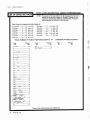
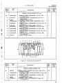
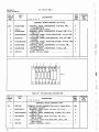
56. AUDIOOSCILLATORCALIBRATION. Calibrate
the audio oscillator as follows:
Do not apply excessive heat to the transistors,
or they will be damaged. Use an adequate heat
sink to the leads when soldering or unsoldering.
Cut leads II necessary.
51. REPAIR OR REPLACEMENT. Individual components of the tester are not to be repaired if defective; replace defective components.
Paragraph
a. Remove the ten screws located near outer edge
of control panel and gently lift panel assembly out
of its case.
Leave the cable assembly connected
to the case.
b. Turn Battery switch to the right and rotate
BETA CAL potentiometer to its maximum position.
Change7
21
I
N
N
CIJ
FUNCTION SELECTOR SWITCH
TYPE
Selector
Switch
PNP
CIRCUIT
IMPEDANCE
Switch
Position
COLLECTOR
VOLTS
Switch
Position
IC
Pot.
Position
NORMAL
0
Min.
0
NORMAL
1.5
Min.
NORMAL
3.0
NORMAL
ICBO
+
E-C
ZOHMS
IC
rI>
BETA READ
BETA CAL
RIN
+
E-B
+
B-C
+
E-C
+
E-B
+
B-C
+
E-C
+
E-B
+
B-C
+
E-C
+
E-B
+
B-C
+
E-C
+
E-B
+
B-C
+
E-C
+
E-B
0
0
0
0
0
0
0
0
0
0
0
0
0
0
()
0
0
+1. 5
0
0
+1. 5
+1. 5
0
+1. 5 +1. 5
0
+1. 5
+1. 5 0
+1. 5
+1. 5
0
+1. 5
+1.5
0
Min.
+3.0
0
0
+3.0
+3.0
0
+3.0 +3.0
0
+3.0
+3.0
0
+3.0
+3.0
0
+3.0
+3.0
0
4.5
Min.
+4.5
0
0
+4.5
+4.5
0
+4.5 +4.5
0
+4.5
+4.5
0
+4.5
+4.5
0
+4.5
+4.5
0
NORMAL
0
Min. -Max
0
0
0
-1. 5
0
+1. 5
,\,,1.5 0
-1. 5
-1. 5
0
+1. 5
-1. 5
0
+1. 5 -1. 5
0
+1. 5
LOW
0
Min. -Max
0
0
0
-4.5
0
+4.5
+4.5 0
-4.5
-4.5
0
+4.5
-4.5
0
+4.5
-4.5
0
+4.5
+
B-C
~
•...
o
::s
.....
"
NPN
+
B-C
+
+
E-C E-B
+
B-C
+
E-C
+
E-B
+
B-C
+
E-C
+
E-B
+
B-C
+
E-C
+
E-B
+
B-C
+
E-C
+
E-B
+
B-C
+
E-C
E-B
0
0
0
0
0
0
0
0
0
0
0
+
NORMAL
0
Min.
0
0
0
0
0
0
0
NORMAL
1.5
Min.
+1. 5
0
0
+1. 5
+1. 5
0
+1. 5 +1. 5
0
+1.5
+1.5
0
+1. 5
+1.5
0
+1. 5
+1. 5
0
!-3
NORMAL
3.0
Min.
+3.0
0
0
+3.0
+3.0
0
+3.0 +3.0
0
+3.0
+3.0
0
+3.0
+3.0
0
+3.0
+3.0
0
P
NORMAL
4.5
Min.
+4.5
0
0
+4.5
+4.5
0
+4.5 +4.5
0
+4.5
+4.5
0
+4.5
+4.5
0
+4.5
+4.5
0
w
w
NORMAL
0
Mill. -Max
0
0
0
-1. 5
0
+1. 5
+1. 5 0
-1. 5
-1. 5
0
+1. 5
-1. 5
0
+1.5
-1. 5
0
+1.5
I
W
LOW
0
Min. -Max
0
0
0
-4.5
0
+4.5
+4.5 0
-4.5
-4.5
0
+4.5
-4.5
0
+4.5
-4.5
0
+4.5
+
B-C
+
E-C
+
E-B
+
B-C
+
E-C
+
E-B
+
B-C
+
E-C
+
E-B
+
B-C
+
E-C
+
E-B
+
B-C
+
E-C
+
E-B
+
B-C
+
E-C
+
E-B
>
....
I
DIODE
NOTE:
NORMAL
0
Min.
0
0
0
0
0
0
0
0
0
0
0
0
0
0
0
0
0
0
NORMAL
1.5
Min.
+1. 5
0
0
0
0
0
0
0
0
0
0
0
0
0
0
0
0
0
NORMAL
3.0
Min.
+3.0
0
0
0
0
0
0
0
0
0
0
0
0
0
0
0
0
0
NORMAL
4.5
Min.
+4.5
0
0
0
0
0
0
0
0
0
0
0
0
0
0
0
0
0
NORMAL
0
Min. -Max
0
0
0
-1. 5
0
+1. 5
+1. 5 0
-1. 5
-1.5
0
+1. 5
-1.5
0
+1. 5 -1.5
0
+1. 5
LOW
0
Min. -Max
0
0
0
-4.5
0
+4.5
+4.5 0
-4.5
-4.5
0
+4.5
-4.5
0
+4.5
0
+4.5
-4.5
N
o
0)
....
I
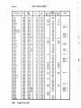
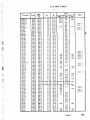
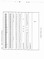
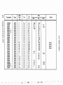
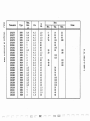
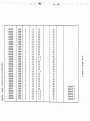
This table shows where the various switches should be placed and what voltages are to be read at the
binding posts of E-C, E-B and B-C. The plus lead of the d-e voltmeter Is indicated by a +slgn over
the pair of binding posts being measured.
Figure 18. Table of Switching Circuit D-C Voltages
r-------i
.
r-'--
r---I
!--...,--
c-·-~
.1
..
t.~;'fi~~J [.- -.
till;:
,..-:-----.
r-~
~a
~
m.~l>lf;I
"""--,j
I .
---:--:--J
.:..1
~J
.; .,' J
Section I
T. O. 33Al-3-206-1
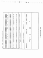
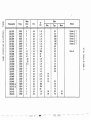
TRANSISTOR
Q1
Q2
Note:
I
·
I
,Xi
L
BASE
COLLECTOR
10K
1800
3800 ohms
4.2V DC
3.9V DC
20.9V DC
0.75V P-P
---
nv
10K
2700 ohms
3800 ohms
4V DC
4.1V DC
20.9V DC
3.1V P-P
3. IV p-p
---
P-P
Place the
Perform all measurements with respect to ground.
positive lead of the ohmmeter to ground.
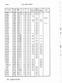
Figure 19. Table of Audio Oscillator Circuit's Voltage and
Resistance Values
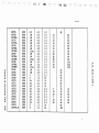
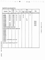
TRANSISTOR
Q3
I
EMITTER
Q4
Q5
Note:
EMITTER
BASE
COLLECTOR
100 ohms
300 ohms
1600 ohms
0.15V DC
0.3V DC
2.9V DC
---
---
0.018V P-P
3000 ohms
1600 ohms
3800 ohms
2. BV DC
2.9V DC
22.5V DC
O.012V p-p
O. oisv p-p
0.13V p-p
900 ohms
1100 ohms
12K
0.92V DC
0.92V DC
12.5V DC
0.025V P-P
0.094V P-P
14.5V P-P
Perform all measurements with respect to ground.
positive lead of the ohmmeter to ground.
Place the
Figure 20. Table of A. C. Amplifier Circuit's
Voltage and Resistance Values
c. Using Multimeter Hickok Model 456, check the
d-e voltages of transistors Ql and Q2 with respect to
ground.
See figure 22 for nominal voltage values.
oscillator is not properly tuned vary the slug of
choke Ll (figure 26) until a single Lissajous pattern is obtained.
d. Using the Oscilloscope Model 1805A, observe
the output waveform of the audio oscillator at the
top of choke L1 (figure 26); it should be a sine wave.
To check the frequency, connect Oscillator Model
202C (set to 1000 cps) to the External sweep circuit of the oscilloscope; make sure the OSCilloscope's
Horizontal display switch is in the External position
and the magnifier is in the 5X posttion.
If the audio
oscillator of the tester is tuned to 1000 cps, a single
Lissajous pattern will be obtained.
If the audio
e. An alternate method of testing the audio oscillator is to connect Electronic Counter Model 523B
to the vertical signal output jack of the oscilloscope.
The oscilloscope's Horizontal display switch should
be in the Main sweep normal position and the magnifier on 1X position.
The input signal to the oscilloscope should be from the top of choke Ll.
Then measure the frequency directly with the electronic counter.
If the audio oscillator needs adjustment, vary the slug of choke Ll until the electronic
23
T.O. 33Al-3-206-1
Section I
PART NUMBER
,OR MODEL
APPLICATION
RANGE
ACCURACY
08cllloscope
'HickokModel
1805Aor 1805
Peak to peak
voltage measurement
dc to
30 mc
Vertical frame
3 db downat .
30mc.
Electroilic Counter.
Hewlett-Packard
Model 523B
Frequency
measurement
10 cps to
1.1 mc
:1:1couut
Hickok Model
1602
Calibration of
amplifier. Measures input voltage across
divider
Imvto
300v
1%between
50cpe and
500kc
Hickok Model
456
'D-c measurement
and resistance
measurement
0-3, 15 .
and 60v .
:1:3%
CaUbrat10n
source
1 cpa 100 kc
:1:2%
NOMENCLATURE
Vacuum Tube
. Voltmeter
.
Multilneter
. Hewlett-Packard
Model202C
Osclllator
Figure 21. Calibration Test Equipment
D-CVOLTAGE
TRANSlS1OR.
EMITTER BASE COLLECTOR
Ql
4.2
3.9
20~9
Q2'
4
4.1
20.9
FJgure 22. Voltmeter D-C Voltages for
Audio Oscillator Transistors
counter reads 1000 cps.
f. Place the oscilloscopeis Horizontal display
Inritch to the Main sweep .normal position and measure the output voltage at the collector of transistor
Q1 (fJPre 32);
The voltage should be 11 volts
P-P : 1. 3 volts. Then measure the voltage across
-the seconclarywinding of transformer Tl (figure 32);
the voltagf/ should be 1. 4 volts P-P :I: O.2 volts.
If·the voltage 18low, .decrease the value of resistor
R4 by paralleling it with a resistor which Is larger
in value than R4; recheck the voltage across the
secondary wind1ngof transformer Tl.
nect ~e1nput of the amplifier across the 10-obm
resistor.. Set the freqUency of the oscillator to 1000
cps and then using the VTVM or oscillosCope, adjust the voltage across' the precision dlvlder to 1
volt P-P. This will give' the amplifie.r a 0.5 my
inPut signaL
d. Rotate the Battery switch to the right. MonitOr
meter of the. tester and vary the frequency do the
variable frequency oscillator.
If the meter doean't
.'peak at 1000 cpa adj\lst the slug of choke 1.3 (figure
26) untU it does. peak at 1000 cps. Then check the
.frequency response of the amplifier from 20 cpa to
approximately 200 kc,
There should be onq ODe
peak and this should occur at 1000cps. If the .amplifier peaks at a low frequency (150 to 400 cpa). replace transistor Q4(figure 29)with a different ZN65lA
transistor.
e. Connect the output of the third stage of the amplifier to the osci11oscope, as shown in figure 24, and
-.measure the a-e voltage. The peak to peak voJtaie
should be witllin 14.5 volts p-p to 15.5 voltll p-p
wblch is sufficient to drive the meter to full lJCale~
set "Fuoctioo Selector to pOsition 13.
D-CVOLTAGE
57. AMPLIFIER CALIBRATION.Calibrate the ampp1ifieras follOws:
.
TRANSISTOR
EMITTER BASE COLLECTOR
a. Turn Battery switch' to .the OPERATEpositiQn.
QS
0.15
0.3
..2.8
b. Using Multimeter .Model 456, check the d-e
voltages of transistors Q3, Q4 andQ5 with respect
to ground.' See figure 23 for DOUdnaI voltage values.
Q4
2.8
2.9
22.5
Q5
0.92
0.92
12.5
c. Disconnect the sbleldedwtre (figure a4) from the
input of the amplifier and connect a precision divider
CODs1stillgof a 20K, 1% resistor and a 10-ohm 1%
resistor to a 'variable frequency oscillator.
Con-
24
Changed 30 September 1963
fc,
Figure 23. Voltmeter D-C Voltages for
Amplifier Transistors
L
L.
L
section I
T.O. 33~1-3-206-1
PRECISION
DIVIDER
TERMINAL BOARD ASSEMSl Y TS1
o
VARIABLE
FREQUENCY
OSCILLATOR
HEWlETI -PACKARD
MODEL 202C
VTVM
w
U
RESISTORS
.0
U
o
\
\
\
\
I,...Ool....-R-3J-e.•••.h.
SHIELDED WIRE
(DISCONNECTED)X$?SXS§I
~
SCREWDRIVER
ADJUSTMENT
~
o
o
:Q
u
OSCILLOSCOPE
HICKOK MODEL 180SA
o
o
POINT B
TERMINAL BOARD ASSEMBLY TB2
Figure 24. Amplifier Calibration Test Set Up
If the output voltage is higher than 15. 5 volts P-P,
adjust the negative feedback resistor R33 by. rotatiDg the screwdriver adjustment counterclockwise
to a smaller value. If the output voltage is less
than 14.5 volts P-P, adjust the negative feedback
resistor R33 bY rotating the screwdriver adjustment clockwise to a higher value.
f. Check the d-e voltage at the collector of the
third
stage
(point
B
is
8round,
figUre
24)'
the voltage should be at least -10 volts de, If it is
less negative, remove resistor R41 (220K)and replace it with a 270K resistor.
Re-check the d-e
voltage.
g. With the oscilloscope connected as shown in
figure 24 (outputof 14.5 volts p-p to 15.5 volts p.P),
check the waveform. The waveform should not be
clipped or bottomed. If the waveform is distorted;
replace resistor R41 with resistors of other values
until the waveform is not distorted.
Note
Don't change the ohmic value of resistor R42
below 10K because this will load the second
stage and shunt the input of the third stage.
h. If all the preceding requirements are met and
the meter is still reading low, decrease the value
Changed 1 March 1965 25
Section I
Paragraphs 58 to 61
T. O. 33A1-3-206-1
of R46 (figure 24) in the detector circuit by paralleling it with another resistor; the total parallel
resistance should not be less than 86K. If the meter
Still reads low, check the diodes (CR3 to CR6) in
the bridge circuit.
After adjusting the value of
resistor R46, the meter should be within ± 2% of
full scale.
58. LARGE KNOB OF Z OHMS CIRCUIT POTENTIOMETER (Rll).
Calibrate the large knob 1K to
lOOK} .of the Z OHMS CIRCUIT potentiometer as
follows:
a. Place a 10K, 1% resistor between the Binding
Posts E and B, using the test lead assembly.
b. Set FUNCTION SELECTOR switch toZ
CIRCUIT.
OHMS
c. Switch the smaller knob (R9) of the Z OHMS
CIRCUIT potentiometer to In Circuit and then rotate
it counterclockwise to its minimum position.
d. Place the CIRCUIT IMPEDANCE switch to NORMAL.
e. Turn the Battery switch to the right and increase the signal by turning BETACALpotentiometer
until the meter reads approximately 1/2 scale.
f. Vary the Z OHMSCIRCUIT potentiometer
knob only) until a null is indicated.
(large
g. Release the Battery switch.
Loosen setscrews
of large know and set the indicator line of the knob
to the 10K point on the inner dial of the Z OHMS
CIRCUIT potentiometers.
Then tighten the setscrews.
59. SMALLKNOBOF Z OHMS CmCUIT POTENTIOMETER (R9). Calibrate the small knob (50 to
500 ohms) of the Z OHMS CIRCUIT potentiometer
as follows:
a. Set the large knob the Z OHMS CIRCUIT potentiometer to its minimum position.
b. Place a 200-ohm, 1% resistor between Binding
Posts E and H, using the test lead assembly.
26
.
c. Place FUNCTIONSELECTOR switch to Z OHMS
CIRCUIT.
d. Turn Battery switch to the right and increase
the stgnal by turning BETA CAL potentiometer until
the meter reads approximately 1/2 scale.
e. Vary the small knob of the Z OHMS CIRCUIT
potentiometer until null is indicated on the meter.
f. Release the Battery switch.
Loosen set screw
of small knob and set the indicator line of the knob
to the 200-ohm point on the outer dial of the Z OHMS
CIRCUIT potentiometer.
Then tighten the setscrew.
60. KNOBOF RIN TRANSISTOR POTENTIOMETER
(RI0). Calibrate the knob (100 ohms to 10K) of the
RIN TRANSISTORpotentiometer as follows:
a. Place FUNCTION SELECTOR switch
TRANSISTOR.
to RIN
b. Switch Z OHMSCmCUIT potentiometer
OF CmCUIT position.
to OUT
c. Place a lK, 1% resistor between the Binding
Posts E and B, using the test lead assembly.
d. Turn Battery switch to the right and increase
the signal by turning BETA CAL potentiometer until
the meter reads approximately 1/2 scale.
e. Vary the Rrn TRANSISTOR potentiometer
null is indicated on the meter.
f. Release
and set the
point on dial
Then tighten
until
the Battery switch.
Loosen setscrews
indicator line of the knob to the 1K
of the RIN TRANSISTOR potentiometer.
the setscrews.
61. FINAL TEST. Perform an "out of circuit"
transistor
test as explained in paragraph 28 and
note its Beta.
Place the same transistor
in a
functionable circuit and perform an "in circuit"
transistor test as explained in paragraph 27 and
note its Beta.
Compare these Beta readings to
the listed Betas in the transistor
manufacturer's
literature.
If this test is' satisfactory, it can be
assumed that the tester is working properly.
,
Section I
T.0.33Al-3-206-1
61A. USE OF'TRANSISTOR REFERENCE CHART
The transistor Reference Chart is to be used a.e a guide in evaluating the quality of transistors.
In an effort to
simplify the Chart as much as po88ible, only the pertinent Information necessary for testing is given. For any
additional information the transistor manufacturer's literature should be consulted.
To explain the use of the Transistor Reference Chart each colum of the chart is described. as follows:
This column specifies the type of transistor
PNP or NPN. The Type Selector switch should be set accordingly.
Max. lebo
'Ibis column specifies the maximum allowable' Jeabte cunent. U the leakap cunent of the transistor under test
exceeds this value it can be conIidend out of to1eruce. ex defectift. The Collectcx Voltage used for this test should
be 4.5V, unlea othenrile noted. 'l1lia test mUll be perfonued out of circuit. see leBO teat procedure in the manual
of operatinl inBtructiona for the Model 890.
~
This is the Collector to Emitter voltage specified for tile Beta test In or Out of Circuit.
Selector Switch should be set accordingly.
The Collector Voltage
Ic
This column gives the Ic current in milliamperes.
The Beta Test should be made at or near this level. The Ie
control adjusts this level when the Function Selector 111 set to the Ic poSition. This adjustment can be made In
or Out of Circuit.
Beta values are given in three columns -- Minimum, Typical, and Maximum, In some cases only Typical Values
are listed. This is because the Transistor Manufacturel' only lists the Typical Value in his specification sheets.
Notes
Nota 1 tbroulb 9 are lilted on pqe 26C.·Tbeae DOt. are aelf-explanatory and u.ed in specific cases·where demtion from CODWDtiOnal
teat proeedure is required,
a..g.d
30~
1969
26A/(26B blank)
T.O.33Al-3-206-1
Section I
MODEL 1890M
TRANSISTOR REFERENCE CHART
NOTES:
I
Note 1:
Perform "leer" test. Reverse the emitter and base leads. Connect a 30 ohm resistor between the emitter
and bue terininals.
Note 2:
Perform "leer" test. Reverse the emitter and base leads. Connect a 200 ohm resistor between the emitter
and bue terminals.
Note 3:
Perform "leer" test. Reverse the emitter and base leads. Connect a 10K ohm resistor between the emitter
and base terminals.
Note 4:
Connect B1 and B2 to the bue terminal and test as triode.
Note 5:
Perform "leer" test. Short emitter and base binding posts and test as for "lebo". Remove jumper for
"Beta" test.
Note 6:
Indicated value for "lebo" is typical, not maximum.
Note 7:
Set Collector Volts (Veb) to 1.5.
Note 8.
Set Collector Volts (Veb) to 3.0.
Note 9.
No "Beta" condition listed.
I
Changed 30 October 1969
26C
T. O. 33Al-3-2Q6-'1
Section I
Transistor
Type
Max.
lebo
Vce
!La
2N2'1
211I34
2N3'5
2"143
2N43A
,2N44,A
2N45
'211I47
211I49
'2N59
2N59A,B.C
2N60,A.t:I.C
2N61,A.M,(
2N63
211I64
2Nh5
2N6B
2N76
2N77
2N7A,A
2 1\1
I:!
1
211194,A
2N'1,)
211I'-17
,A
2N':IH.A
211I':19
2N101
2NI02
2NI04
2NI05
2NI06
2NI07
2NI09
2Nll1
2Nl12
2N113
2N114
2Nl11
2NIIH
2N118A
2N 11 'I
2N120
2"1123
2""125
2N12b
2N128
2N129
lN130.A
2N131,A
2N132.A
2N133
2N135
2N13b
2N137
2N136
2"1139
2N140
2N141
2N142
2N143
2N144
2N145
2N146
2N147
2"1156
2N158
2N158A
26D
NI'N
005.0
PNjJ
016.0
III!)III 016.0
PNP
005.0
PllljJ
005.0
PNP
005.0
PNP
005.0
PNP
003.0
PNP
003.0
PNP
007.0
PiliP
007.0
JJNjJ
007.0
PiliP
007.0
PNP
006.0
JJNjJ
006.0
PiliP
006.0
1'11I1' 002. 5 1'1
A
PiliP
010.0
I'NI'
006.0
NPN
001.5
I'NI'
006.0
11I1'11I 014.0
NI'III
002.5"'A
IIII'N
002.0
III!)III OlD.O
NI'N
010.0
002.51'1A
PNI'
IIII'N
002.,MA
I'NP
006.0
PiliI'
003.0
I'NI'
012.0
1'11I1' OOb.O
PiliP
006.0
PiliP
001.0
PNP
001.0
1'''11' 001.0
PNP
001.0
NPN
000.8
NPN
OOU.R
N •.•
N
OOO.I:!
NPN
000.8
000. I:!
NPN
PNP
003.0
(J02.0
NI'N
NI'N
002.0
,)03.0
PNI'
PNP
003.0
PNP
006.0
006.0
PNP
PNP
006.0
PNP
012.0
PNP
005.0
PiliI'
005.0
PNI'
005.0
PN;'
006.0
PNP
004.0
I'NP
004.0
PNP
002.0M.A
002.0fillA
NPN
PNP
002.0MA
NPN
002.0MA
NPN
003.0
NjJN
003.0
NPN
003.0
.400.0
PNP
PNP
300.0
PNP
250.0
Changed 13 June 1969
4.5
4.5
4.5
4.5
4.5
4.5
4.5
4.5
4.5
4.5
4.5
4.5
4.5
4.5
4.5
4.5
4.5
4.-5
4.5
4.'S
4.5
4.5
4.5
4.5
4.5
4.S
4.5
4.5
4.,)
4.,)
1.5
4.5
1.5
4.5
4.5
4.5
4.5
4.5
4.5
4.5
4.5
4.5
4.5
4.5
4.5
3.0
3.0
4.5
4.1)
4.5
1.5
4.5
4.5
4.5
4.5
4.5
4.5
1.5
1.5
1.5
1.5
4.,>
4.5
4.5
1.5
1.5
1.5
Beta
Ie
ma
01.0
01.0
01.0
01.0
01.0
01.0
01.0
01.0
01.0
10.0
10.0
10.0
10.U
01.0
01.0
01.0
99.9
01.0
00.7
01.0
01.0
01.0
99.9
OO.'S
01.0
01.0
9<J.'1
9<J.9
01.0
00.7
00.5
01 .0
50.()
01. u
01.0
01.0
01.0
01.0
01.(;
01.0
01.0
01.0
01.0
01.0
01.0
00.5
00.5
01.0
01.0
01.0
00.5
01.0
01.0
01.0
01.0
01.0
01.0
99.9
99.9
Min.
99.'9
Notes
04'-J
025
030
030
009
009
032
020
020
125
042
042
025
012
039
039
110
110
090
065
022
04'>
090
035
019
055
051::1
066
01f>
200
060
0110
025
OO<J
01t1
018
036
076
031
019
012
020
060
040
040
045
065
012
024
03'1
04'1
099
090
036
074
040
021
022
045
090
NUTE
NUTE
6
6
NUTE
NIITE
NUT,E
NlITE
6
6
6
2
NUTE
NOTE
3
2
NOTE
NUTE
2
2
NUTE
8
NOTE
NlITE
NUTE
NUTE
6
6
6
6
NOn:
6
NOTE
6
NOTE
NOTE
NelTE
NOTE
2
2
2
2
0'1'1
035
013
040
040
035
035
044
055
020
040
090
0'10
332
066
039
025
022
022
99.'1
'i9.9
99.9
Max.
075
99.9
01.0
01.0
01.0
Typ.
020
040
060
140
048
048
015
015
015
015
030
033
036
055
04!>
()45
110
110
.
Ii
~
T. O. 33Al-3-206-1-
Tra'lsistor
Max.
Type
lebo
Ie
ma
Vee
j..la
'2N160,A
:2N161,A
;2N162"A
.2N163,A
1N164A
\ 2N165
i 2111167,A
211I168
:2N169
;2111169A
711I170
r2N"17.&.A
I
,211I175
21111115
2/11186
'2/11186A
211I1117
l/11l117A
7/111118
21111118A
211I189
2/11190
,211I191
, 211I192
. 7.11I193
2111194A
,2",195
211I200
211I204
,21112U5
211I206
211I207
2111207A,"
211I211
211I212
211I213
2111213A
2111214A
.211I215
211I216
211I217
211I218
2N219
211I220
211I223
2N21.4
211I225
2N226
,211I227
2N228
211I229
2N232
'7.N233A
::'l
-211I233
ZN23A
I
ZN240
211I241
2111241A
ZN243
2N244
2N247
2N248
211I264
211I265
2N269
,2N274
J
ZN279
.:211I280
NI'N
NP/II
N!JN
NPN
/IIPN
NPN
NP/II
NPIII
IIIPN
IIIPN
N•.•
N
iPNP
002.0
002.0
002.0
002.0
000.5
002.5
00U.8
000.5
000.5
002.5
003.0
008.0
01.0
01.0
01.0
01.0
01.0
01.0
01.0
01.0
01.0
4.5
4.5
4.5
4.5
4.5
4.5
4.5
4.5
1.5
(H.O
4.5
4.5- , 01.0
01.2
2.0
Beta
Min.
Typ. ,
Max.
009
, 019
039
039
013
024 \
019
039
r
;
099 I
040 i
050 ,
200
066
040
072
050
OZO
055
065
040
030
030
045 ,['
045
060
060
032 ,
042 i
020
'
00.5
PN...
005.0
4.5
02.0
PN...
007.0
4.5
50.0·
1.5
PNP
006.0
50.0
1.5
PNP
006.U
50.0
1.5
PNP
OU6.0
50.0
1.5
P/IIP
006.0
50.u
1.5
PNP
006.0
10.0
1.5
PNP
UQ7-.0
01.0
4.5
PNP
006.5
01.0
4.5
PNI'
006.5
01.0
4.5
PiliP
006.5
Ul.0
4.5
PiliP
006.5
01.0
4.5
NPN
015.0
01.0
4.5
NPN
015.0
100
01.0
4.5
PiliP
003.0
030
01.0
4.5
PNI'
002.0
050
01.0
4.5
PNP
002.0
015
01.0
4.5
PNP
OOZ.O
•.•
IIIP
004.0
01.0
4.5
035
01.0
4.,5
PNP
009.0
035
01.0
4.5
PNP
006.0
010
4.5
01.0
NPN
013.0
4.5
01.0
NPN
015.0
070
01.0
4.5
NPN
016.0
100
01.0
4.5
NPN
016.0
10.0
1.5
PNP
006.5
-tr.'j01.0
PNP
006.0
01.0
4.5
NPN
025.0
050
01.U
4.5
PNP
002.5
022
01.0
PNP
004.0
4.5
022
01.0
4.5
PNP
004.0
00.5
4.5
I'NP
007.0
070
01.0
4.5
PNP
014.0
10.0
4.5
PNP
015.0
ATCHED
PNP
PAIR OF 2N224 WI H RETA
l'iIIP 010.0
10.0
~.5
ATCHED
PNP
PAIR OF 2N226 WI H BETA
4-:-SN•.•
N
054.0
055
10.0
025
4.5
01.0
N"'N
065.0
PiliP
006.0
009
00.5
3.0
NPIII
015.0
4.5
010
01.0
010
01.0
4.5
NPN
033.0
PNP""-010.0
OZ.o
4.5
016
PNP
010.0
00.5
3.0
PNP
006.0
50.0
1.5
50.0
.1.5
PNP
006.0
4.5
NPN
000.4
05.0
05.0
4.5
NPN
000.4
4.5
PNP
004.0
01.0
00.5
4.5
PNP
010.0
4.5
NPN
000.5
020
10.0
4.5'
PiliP
006.5
01.0
4.5
PNP
003.0
01.0
PiliP
007.0
4.~
01.0
"00.5
020
PNP
012.0
1.5
~1.5
PiliP
012.0
030
03.0
Notes
NOTF
6
!'fUH-
h
IIIOTE
NOTE
h
h
i
~~~I
040
040
NIITE 3
I
I
NUT!:
lau i
045
I
080
:
025·
047
100
100
I
300
060
lZO
035
020
3
NOTE H
NUTE: 6
NUTE
NuTE
6
6
NOTF
3
NOTE
3
NUTE
3
250
250
080
044
045
o
o
048
048 ,
065 i
110 i
080 i
WITHt
070
WITH)
100
110
110
150
20""
20%
100
075
NOTE
3
NOTE
3
NOTE
3
039
040
030
070
070
016
031
060 '
020
055
110
135
060
030
041
Change 8
040
015
26E
,
r. O.
Section I
33Al-3-206-1
I
t
Transistor
Type
Max.
lebo
l1a
2N281
2N282
2N283
2N284A
2N284
2N292
2N293
2N299
2N300
2N306
2N311
2N312
2N315A
2N316
2N317
2N316A
2N317A
2N319
2N320
2N321
2N322
2N323
2N324
2N327A
2N327
2N327A
2N328A
2N328
2N328fl
2N329A
2N329
2N3298
2N330A
2N330
2N331
2N33lA
2N332
2N333A
2N333
2N334A
2N334
2N335A,B
2N335
'2N336A
2N336
2N337A
2N337
2N338A
2N338
2N339A
2N339
2N340A
i 2N340
!
2N341A
, 2N341
c
2N342,A,H
2N343.B
2N344
2N345
2N346
2N354
2N355
2N356A
2N356
2"<357A
2"'357
?N358A
PNP
PNP
PNP
PNP
PNP
NPN
NPN
PNP
PNP
Nf.'N
PNP
NPN
PNP
PNP
PNP
PNP
PNP
PNP
PNP
PNf.'
PNP
PNP
PNP
PNP
PNI-'
PNI-'
PNP
PNP
PNP
PNP
PNP
PNP
flNP
Pi'll-'
PNfJ
NI-'N
NPN
NPN
Nf.'N
NPN
NI-'N
NflN
NPN
NPN
NPN
NPN
NPN
NPN
NPN
NPN
NPN
NPN
NPN
NPN
NPN
NPN
NPN
PNP
PNI-'
PNP
PNP
PNP
NI-'N
NPN
NPN
NPN
NPN
26 F
Changed 13 June 1969
I
i
"
Vce
Ie
ma
006.0
4.5
10.0
PAIR OF 2N281 WI H BETA
006.0
4.5
00.5
006.0
4.5
10.0
006.0
4.5
10.0
000.5
1.5
01.0
000.5
1.5
01.0
003.0
3.0
00.5
003.0
3.0
00.5
009.0
4.5
01.0
025.0
1.5
10.0
003.0
1.5
01.0
002.0
4.5
01.0
002.0
1.5
50.0
002.0
1.5
50.0
002.0
4.5
01.0
002.0
4.S
01.0
006.5
I.S
20.0
006.5
1.5
20.0
00b.5
I.S
20.0
008.0
4.5
01.0
008.0
4.5
01.0
008.0
4.5
01.0
040.0NA
4.S
03.0
050.0NA
4.5
01.0
000.4NA
1.5
01.0
040.0NA
4.5
03.0
050.0NA
4.5
01.0
000.4NA
01.0
1.5
040.0NA
4.5
03.0
050.0NA
4.5
01.0
000.4NA
1.5
01.0
000.4
4.5
03.0
O,)O.ONA
·4.5
01.0
006.0
4.S
01.0
002.0NA
4.5
01.0
000.8
4.5
01.0
OOl.ONA
4.5
01.0
000.8
4.5
01.0
002.0NA
4.5
01.0
000.8
4.5
01.0
002.0NA
4.5
01.0
000.8
4.5
01.0
002.0NA
4.5
01.0
000.8
4.5
01.0
040.0NA
4.5
01.0
000.5
4.5
01.0
040.0NA
4.5
01.0
000.5
4.5
01.0
000.4
4.5
01.0
000.4
4.5
05.0
000.4
4.5
01.0
000.4
4.5
05.0
000.4
4.5
01.0
000.4
4.5
OS.O
4.5
000.4
05.0
000.4
4.5
05.0
003.0
3.0
00.5
003.0
00.5
3.0
003.0
3.0
00.5
070.0NA
4.5
01.0
070.0NA
4.5
01.0
005.0
4.5
01.0
005.0
4.5
01.0
005.0
4.5
01.0
005.0
4.5
01.0
005.0
4.5
01.0
Beta
Min.
Typ.
Notes
Max.
070
ATCHED
0 WITHI
30~
040
045
045
050
050
025
040
009
006
025
025
065
065
050
050
070
050
120
130
180
034
050
080
045
068
085
014
0·14
NOTE 6
NOTE 6
090
090
125
NOTE 7
o lI'l
02A
018
009
036
014
009
030
009
009
018
018
018
018
037
037
07&
076
015
009
01S
009
015
009
009
028
011
02S
010
009
009
024
036
060
050
072
025
030
05"0
016
015
030
030
038
039
052
060
095
120
050
OSO
080
080
072
070
022
022
044
044
090
090
090
090
333
333
090
090
022
035
035
018
090
090
090
090
031
090
033
110
1-'
I
t._...:.
ois
060
030
090
04')
120
/ ..
T. o. 33Al-3-206-1
Transistor
Type
Max.
lebo
Vce
Ila
2N35B
2,...359
2N360
2N361
2N362
2N363
211I364
2N365
2N366
2N367
2N368
2N369
2N370
2N371
2N372
2N373
2N374
2N377
2N381
2N382
2N383
2N384
2N385
2N3854
2N3884
2N388
2N393
2N394
2N395
2·N396,4
2N397
2N398A
2N3988
2N402
2N403
2N404,4
2N405
2N406
2N407
2N408
2N409
2N410
2N411
2N412
2N413A
2N413
2N414A
2N414
2N416
2N417
2N422
2N425
2N426
2N427
2N428
2N438,A
2N439,A
2N440,A
2N444A
2N444
2N445A
2N445
2N446A
2N446
2N447A
2N447
2N4418
-
"
,
NPN
PNP
PNP
PNP
PNI'
PNP
NPN
NPN
NPN
PNP
PNP
PNP
PNP
PNP
PNP
PNP
I>NP
NPN
PNP
PNP
PNP
PIIlP
NPN
NI>N
NI'N
NPN
PNP
PNP
PNP
PNP
I>NI>
PNP
I>NP
PNI>
PNI'
PNP
PNP
PNP
PfooIP
PNP
PNI>
PNP
PNI>
PNP
I>NP
I>NI'
PNI'
PNP
PNP
PNP
PNP
PNP
PNP
PNP
PNP
NPN
NPN
NPN
NPN
NPN
NPN
NPN
NPN
NPN
NPN
NPN
NPN
005.0
009.0
009.0
Q09.0
009.0
009.0
004.0
004.0
004.0
008.0
008.0
008.0
012.0
012.0
012.0
005.0
005.0
004.0
006.0
006.0
006.0
007.0
004.0
004.0
013.0
004.0
005.0
004.0
003.0
003:.0
004.0
014.0
006.0
007.0
007.0
003.0
008.0
008.0
008.0
008.0
008.0
003.0
003.0
003.0
003.0
003.0
003.0
003 •.
0
003.0
003.0
007.0
004.0
004.0
004.0
004.0
004.0
004.0
004.0
004.0
004.0
004.0
004.0
004.0
004.0
004.0
004.0
004.0
4.5
4.5
4.5
4.5
4.5
4.5
4.5
4.5
4.5
4.5
4.5
4.5
4.5
4.5
'4.5
4.5
4.•5
1.5
4.5
4.5
4.5
4.5
1.5
1.5
4.5
4.5
3.e
1.s
1.5
4.5
1.5
4.5
4.5
4 •.
5
4.5
4.5
4.5
4.5·
1.5
1.5
4.5
4.5
4.5
4.5
4.5
4.5
4.5
4.5
4.5
4.5
4.5
1.5
1.5
1.5
1.5
4.5
4.5
4.5
4.5
4.5
4.5
4.5
4.5
4.5
4.5
4.5
4.5
Beta
Ie
ma
01.0
01.0
01.0
01.0
01.0
01.0
01.0
01.0
01.0
01.0
01.0
01.0
01~0
01.0
01.-0
01.0
01.0
30.0
10.0
10.0
10.0
01.5·
30.0
30.:>
01.0
01.0
OQ.5
10.0
'10.0
01.0
10·.0·
01.0
01.0
01.0
01.0
01.0
01.0
01.0
50.0
50.0
01.0
01.0
01.0
01.0
01.0
01.0
01.0
01.0
01.0
01.0
01.0
30.0
40.0
55.0
04.0
01.0
01.0
01..0
01.0
01.0·
01.0
01.0
01.0
01.0
01.0
·01.0
01.0
Section I
Notes
Min.
019
049
035
070
090
040
Typ.
060
150
100
070
090
O~O
015
026
065
015
036
055
055
055
055
055
055
030
060
090
115
060
060
060
125
125
155
070
060
070
085
Max.
-
049
142
085
135
'155
NOTE A
NOTE II
020
040
J20
022
022
022
020
010
030
030
025
015
015
015
015
010
035
020
060
030
085 .
050.150
020
'032
135
035
035
060
060
04Q
048
048
050
030
060
080
110
110
110
080
050
090
090
080
140
050
030
040
055
100
025
035
065
025
NOTE
NOTE
NOTE
NOTE
7
7
7
7
070
120
150
250
atanged 13 June 1969
26G
T. O. 33Al-3-206-1
.
Transistor
Type
Max.
lebo
Vce
~a
2N44B
NPN
2N449
NPN
2N450
2.N460
PNP
PNP
PNP
PNP
PNP
PNP
PNP
NPN
NPN
NPN
NPN
NPN
NPN
NPN
NPN
NPN
NPN
NPN
NPN
NPN
NPN
NPN
NPN
NPN
PNP
PNP
PNP
PNP
PNP
PNP
PNP
PNP
NPN
NPN
PNP
PNP
PNP
PNP
PNP
PNP
PNP
PNP
PNP
NPN
NPN
NPN
PNP
PNP
PNP
PNP
PNP
PNP
PNP
PNP
PNP
PNP
PNP
PNP
PNP
PNP
PNP
PNP
PNP
PNP
2N461
2N464
2N465
2N466
ZN467
ZN470
ZN411A
2N411
2N472A
2N472
2N473
2N474A
ZN474
2N475A
2N415
2N416
2N411
2N418
2N479A
2N419
2N480A
2N480
2N48l
2N482
2N483
2N484
2N485
2N486
2N495
2N496
2N497.A
2N498.A
2N499
2N501,A
2N502A
2N502
2N503
2N504
2N508A
2N508
ZN509
2N515
2N51b
•
2N517
2N518
2N519,A
2N520A
2N520
2N5Z1
2N521A
2N5Z2
ZN5ZZA
2N5Z3
2N52~.
2N52~
2N5Z5
2N5Z6,A
ZN527,A
2N534
ZN535,A,8
2N536
2N537
. ~'_~~~!8iA'
26B
;~.
ChangeS
000.5
000.5
004.0
005.0
005.0
009.0
009.0
009.0
009.0
003.0NA
000.2
000.2
l50.0NA
l50.0NA
003.0NA
000.2
000.2
150.0NA
150.0NA
003.0NA
000.2
003.0NA
000.2
000.2
l50.0NA
150.0NA
006.0
006.0
006.0
006.0
006.0
006.0
000.4
060.0NA
004.0
004.0
005.0
005.0
003.0
003.0
003.0
006.0
003.0
003.0
002.5
002.0
002.0
002.0
004.0
002.0
002.0
002.0
002.0
002.0
002.C
002.0
002.0
OOZ.O
004.0
004.0
004.0
004.0
006.0
002.5
1.5
1.5
4.5
4.5
4.5
4.5
4.5
4.5
4.5
4.5
4.5
4.5
4.5
4.5
4.5
4.5
4.S
4.5
4.5
4.5
4.5
4.5
4.5
4.5
4.5
4.5
4.5
4.5
4.5
4.5
4.5
4.5
4.5
1.5
4.5
4.5
4.5
4.5
4.5
4.5
4.5
4.5
4.5
4.5
4.5
4.5
4.5
4.5
1.5
4.5
4.5
4.5
4.5
4.5
4.5
4.5
4.5
4.5
4.5
4.5
4.5
4.5
4.5
4.5
1.5
4.5
_ 6~J;~
__~{~5
oo~.o
OOb.O
I -
c.
ma
01.0
01.0
01.0
01.0
01.0
01.0
01.0
01.0
01.0
01.0
01.0
01.0
01.0
01.0
01.0
01.0
01.0
01.0
01.0
01.0
01.0
01.0
01.0
01.0
01.0
01.0
01.0
01.0
01.0
01.0
01.0
01.0
01.0
15.0
30.0
30.0
02.0
02.0
02.Q
02.0
02.0
01.0
01.0
01.0
01~0
01.0
01.0
01.0
10.0
01.0
01.0
01.0
01.0
01.0
01.0
01.0
01.0
01.0
01.0
01.0
01.0
01.0
01.0
01.0
10.0
10.0
Beta
Min.
008
016
032
014
027
054
110
010
010
010
010
010
020
020
020
020
020
030
030
040
040
040
040
040
015
015
009
009
016
015
060
015
040
020
035
070
060
100
080
125
018
030
044
060
035
035
009.
Notes
Typ.
Max.
025
072
130
051
035
017
017
017
035
035
035
045
045
060
060
060
050
050
060
090
050
100
030
012
030
030
035
040
065
065
045
110
110
049
028
033
033
066
130
260
025
025
025
025
025
050
050
050
050
050
060
060
100
100
100
100
100
(
I
NOTE 6
NOTE 6
.
t.-
r:~
!
(
<~~
\1/
I~
(~
1':1;1
,"1
/:t~
i
t.
rti.;
lIi
180
r;~
L-"l
025
100
040
070
150
1Z0
200
ZOO
300
030
044
.064
080
100
100
150
I
\
041
064
088
120
200
200
of~_ -08~ i '~~~~
200
..
'lilt
••
I
o
iiS
~
CD
Q.
....•
~
'1
I::
....•
co
0)
0)
N
CJ)
1-4
2N232
2N233
2N233A
2N238
2N240
2N241
2N241A
--
;PNP
NPN
NPN
PNP
PNP
PNP
PNP
2N242
I>NP
2N243
2N244
2N247
2N248
2N265
2N269
2N274
2N279
2N280
2N281
2N282
2N28:3
2N284
2N284A
2N292
2N29:3
2N299
2N300
2N306
2N311
2N312
2N315
NPN
NPN
PNP
PNP
;PNP
PNP
PNP
PNP
PNP
PNP
PNP
PNP
PNP
PNP
NPN
NPN
PNP
PNP
NPN
PNP
NPN
PNP
6
33
25
10
10
6
6
0.15MA
0.4
0.4
f)
:10
6.5
3
3.0
4.5
4.5
4.
5
0.5
1.0
1.0
2.0
p. 5
50
50
9
~O
10
40
30
70
70
O.lA
55
10
~5
10
40
1.0
,55
4. 5
4.5
0.5
20
4.5
110
~.0
1.5
24
24
7
1.0
60
~.5
1.5
12
O.5
20
30
1.0
12
4.5
47
30
'6
4.5
10
70
'Pairof 2N281 withBeta matched to within30%
1.0
6
4.5
40
6
4.5
10
47
6
4.5
10
47
1.0
0.5
4.5
25
1.0
0.5
4.5
25
:3
3.0
O. 5
11
18
:3
3.0
O. 5
18
1.0
25
4.5
16
75
1.5
25
10
50
1.5
3
10
50
1.5
2
50
25
3.0
1.5
1.5
4.5
4.5
~.5
39
Note 4
Note 4
16
Note 7
.1-3
.ow
40
82
w
>
•...
I
W
I
~
o
CJ)
I
•....
Note 6
Note 6
33
Note 7
'~.>
~~:,
'''''~,;,w;1I
!:S~~
i~)
.:i~.~
••
I
~
~
t'D
Q.
•....
~
"1
1=
•....
co
0)
0)
N
(J)
I-t
"
2N232
2N233
2N233A
2N238
2N240
2N241
2N241A
2N242
2N243
2N244
2N247
2N248
2N265
2N269
2N274
2N279
2N280
2N281
2N282
2N283
2N284
2N284A
2N292
2N293
2N299
2N300
2N306
2N311
2N312
2N315
PNP
NPN
NPN
PNP
PNP
PNP
~-~P
PNP
NPN
NPN
PNP
PNP
PNP
PNP
PNP
'PNP
PNP
PNP
PNP
PNP
PNP
PNP
NPN
NPN
PNP
PNP
NPN
PNP
NPN
PNP
6
3.0
0.5
9
1.0
33
4.5
10
1.0
25
4.5
10
10
4. 5
2.0
40
10
3.0
0.5
16
30
6
1.5
50
70
1.5
6
~O
70
O.15MA
4.5
O.lA
55
0.4
4.5
10
~5
0.4
10
40
~. 5
1.0
6
4.5
.55
~10
4.5
0.5
20
6.5
4.5
110
1.0
1.5
3
24
24
'7
1.0
4.5
60
1.5
12
0.5
20
30
1.0
12
4.5
30
47
'6
4.5
10
70
'Pairof 2N281 with Beta matched to within30%
1.0
6
4.5
·40
6
4.5
10
47
6
4.5
10
47
1.0
O.5
4.5
25
O.5
4.5
1.0
25
3
3.0
O.5
11
18
3
3.0
0.5
18
1.0
25
4.5
16
75
1.5
25
10
50
1.5
3
10
50
1.5
2
50
25
39
Note 4
Note 4
I
Note 7
.o
.
t-i
Co)
Co)
40
82
>
•..•
I
Co)
I
~
o
(J)
I
•..•
Note 6
Note 6
33
Note 7
2N335A, B
2N336
2N336A
2N337
2N337A
2N338
2N338A
2N339
2N339A
2N340
2N340A
2N341
2N341A
2N342
2N342A
2N342B
2N343
2N343B
2N344
2N345
2N346
2N354
2N355
2N356
2N356A
2N357
2N357A
2N358
2N358A
NPN
NPN
NPN
NPN
NPN
NPN
NPN
NPN
NPN
NPN
NPN
NPN
NPN
NPN
NPN
NPN
NPN
NPN
PNP
PNP
PNP
PNP
PNP
NPN
NPN
NPN
NPN
NPN
NPN
0.2
0.8
0.2
0.5
.04
O.5
.04
0.4
0.4
0.4
0.4
0.4
0.4
0.4
0.4
0.4
0.4
0.4
3
3
3
O.1
O.1
5
5
5
5
5
5
4.5
4.5
4.5
4..5
4.5
4.5
4.5
4.5
4.5
4.5
4.5
4.5
4.5
4.5
4.5
4.5
4.5
4.5
3.0
3.0
3.0
4.5
4.5
4.5
4.5
4.5
4.5
4.5
4.5
1.0
1.0
1.0
1.0
1.0
1.0
1.0
10
5.0
10
5.0
10
1.0
10
10
1.0
10
1.0
O.5
O.5
O.5
1.0
1.0
1.0
1.0
1.0
1.0
1.0
1.0
37
76
76
19
19
39
19
10
25
10
25
10
25
10
10
7
25
20
11
25
10
9
9
52
120
95
55
55
99
55
90
90
90
90
.~
p
w
w
32
>I-"
I
22
35
20
18
18
30
60
45
90
60
120
90
33
110
35
W
I
N
o
C1)
I
I-"
N
(j)
r-
j
('D
~
~
en
~
(")
('D
~
('D
"1
~
<0
(j)
~
rr-·'----.',
Transistor
2N359
2N360
2N361
2N362
2N363
2N364
2N365
2N366
2N367
2N368
2N369
2N370
2N371
2N372
2N373
2N374
2N377
2N381
2N382
2N383
2N384
2N385
2N385A
2N388
2N388A
2N393
Type
PNP
PNP
PNP
PNP
PNP
NPN
NPN
NPN
PNP
PNP
PNP
PNP
PNP
PNP
PNP
PNP
NPN
PNP
PNP
PNP
PNP
NPN
NPN
NPN
NPN
PNP
r++:
Max.
lebo
lJ.a
9
9
9
9
9
4
4
4
8
8
8
12
12
12
5
5
4
6
6
6
7
4
4
5
5
5
;".,,-::----.
{f;t25~
Beta
Ie
Vee
ma
4.5
4.5
4.5
4.5
4.5
4.5
4.5
4.5
4.5
4.5
4.5
4.5
4.5
4.5
4.5
4.5
1.5
4.5
4.5
4.5
4.5
1.5
1.5
1.5
1.5
3.0
1.0
1.0
1.0
1.0
1.0
1.0
1.0
1.0
1.0
1.0
1.0
1.0
1.0
1.0
1.0
1.0
30
10
10
10
1.5
30
30
30
30
O.5
Min.
~-'".---~
~'"
~;~.f'ji~l~t;:i.
35
70
90
20
40
Typ.
150
100
70
120
50
15
26
65
15
36
55
55
55
55
55
55
30
60
90
115
60
60
60
100
100
155
~~'1' ~
Notes
Max.
.ot-:I
.c,..,.
c,..,
>
••••
c,..,I
I
N
o
(j)
I
•....
85
135
135
175
Note 7
Note 7
[-1'
~~~~
••.•.••.••
---~'7
l.
l
t '
I.:
f~.~~
~~
o
I
~
•...
C1I
~
(")
g.
<t>
<t>
"1
•...
CD
en
.a:o.
N
c:n
==
2N394
2N395
2N396,A
2N397
2N398
2N398A
2N402
2N403
2N404,A
2N405
2N406
2N407
2N408
2N409
2N410
2N411
2N412
2N413
2N413A
2N414
2N414A
2N416
2N417
2N~22
2N425
2N426
2N427
2N428
2N438
PNP
PNP
PNP
PNP
PNP
PNP
PNP
PNP
PNP
PNP
PNP
PNP
PNP
PNP
PNP
PNP
PNP
PNP
PNP
PNP
PNP
PNP
PNP
PNP
PNP
PNP
PNP
PNP
NPN
.~ ••
'),
4
3
3
4
14
14
7
7
3
8
8
8
8
6
6
6
6
3
3
3
3
3
3
7
4
4
4
4
4
1.5
1.5
1.5
1.5
1.5
1.5
4.5
4.5
4.5
4.5
4.5
1.5
1.5
4.5
4.5
4.5
4.5
4.5
4.5
4.5
4.5
4.5
4.5
4.5
1.5
1.5
1.5
1.5
4.5
10
10
10
10
5.0
5.0
1.0
1.0
1.0
1.0
1.0
50
50
1.0
1.0
0.6
0.6
1.0
1.0
1.0
1.0
1.0
1.0
1.0
30
40
55
4.0
1.0
t~""
20
30
50
70
15
70
60
80
85
60
60
20
32
135
35
35
60
60
48
48
75
75
30
25
60
60
80
140
50
30
40
55
100
25 ~_
Note 8
.~
.o
Co)
Co)
>•....
I
Co)
I
N
o
C7)
120
I
•....
200
-
Note 7
Note 7
Note 7
Note 7
N
0)
Z
~
'J&
(1)
Po
~
tJ1
t:1
(1)
(")
(1)
~
.,
(1)
~
co
0)
~
~~--.~,;.---.-:..
Transistor
2N438A
2N439
2N439A
2N440
2N440A
2N444
2N444A
2N445
2N445A
2N446
2N446A
2N447
2N447A
2N448
2N449
2N450
2N460
2N461
2N464
2N465
2N466
2N467
2N470
2N471
2N471A
2N472,A
Type
NPN
NPN
NPN
NPN
NPN
NPN
NPN
NPN
NPN
NPN
NPN
NPN
NPN
NPN
NPN
PNP
PNP
PNP
PNP
PNP
PNP
PNP
NPN
NPN
NPN
NPN
Max.
lebo
Jla
Vce
Ie
ma
4
4
4
4
4
4
4
4
4
4
4
4
4
0.5
O. 5
4
3
3
7
7
7
7
5na
5na
5na
5na
4. 5
4. 5
4.5
4. 5
4. 5
4.5
4.5
4.5
4.5
4.5
4.5
4.5
4.5
1.5
1.5
4.5
4.5
4.5
4.5
4.5
4.5
4.5
4.5
4.5
' 4.5
4.5
1.0
1.0
1.0
1.0
1.0
1.0
1.0
1.0
1.0
1.0
1.0
1.0
1.0
1.0
1.0
1.0
1.0
1.0
1.0
1.0
1.0
1.0
1.0
1.0
1.0
1.0
~.,!-
;~a,.&'
Beta
Min.
15
15
15
15
15
10
15
20
35
30
60
50
85
8
14
27
56
112
10
10
10
10
Typ.
Max.
25
35
35
65
65
15
25
35
70
60
120
125
150
25
72
130
24
49
26
45
90
180
16
16
16
16
Notes
.•~
p
Co)
Co)
>~
I
51
Co)
Note 6
'Note 6
I
N
o
0)
I
~
25
25
25
25
i~tI)
"~"~""'~"""~'\'
~
o
~
~
(1)
0..
•....
U1
tj
<"D
t~
ro
S
IS'
.,
('!J
•....
(0
0')
~
~
0')
o
2N473
2N474
2N474A
2N475,A
2N476
2N477
2N478
2N479
2N479A
2N480
2N480A
2N481
2N482
2N483
2N484
2N485
2N486
2N495
2N496
2N497,A
2N498, A
2N499
2N501
2N50lA
2N502
2N502A
2N503
2N504
2N508
NPN
NPN
NPN
NPN
NPN
NPN
NPN
NPN
NPN
NPN
NPN
PNP
PNP
PNP
PNP
PNP
PNP
PNP
PNP
NPN
NPN
PNP
PNP
PNP
PNP
PNP
PNP
PNP
PNP
5na
5na
5na
5na
5na
5na
5na
5na
5na
5na
5na
6
6
6
6
6
6
0.4
.06
4
4
5
5
5
3
3
3
10
8
~
~
4.5
4.5
4.5
4.5
4.5
4.5
4.5
4.5
4.5
4.5
4.5
4.5
4.5
4.5
4.5
4.5
4. 5
4. 5
1.5
4.5
4.5
4.5
4.5
4.5
4.5
4.5
4.5
4.5
4.5
1.0
1.0
1.0
1.0
1.0
1.0
1.0
1.0
1.0
1.0
1.0
1.0
1.0
1.0
1.0
1.0
1.0
1.0
15
30
30
2.0
2.0
2.0
2.0
2.0
2.0
1.0
1.0
20
20
20
20
30
30
40
40
40
40
40
15
9
15
9
.&ii
30
30
30
30
45
45
60
60
60
60
60
50
50
60
90
50
100
30
12
30
30
35
40
40
65
65
45
16
112
50
50
50
50
60
60
100
100
100
100
100
.,
.p.
,
w
w
>•....
I
W
I
~
o
0')
•....
I
Type
Max.
Icbo
ua
Vee
Ic
ma
PNP
N?N
NPN
NPN
PNP
PNP
PNP
PNP
PNP
PNP
PNP
PNP
PNP
PNP
PNP
PNP
PNP
PNP
PNP
PNP
PNP
PNP
PNP
PNP
PNP
NPN
2.5
25
25
25
4
2.5
2
2
2
10
2
10
2
10
2
4
4
4
4
5
6
6
6
6
2.5
5na
4.5
4.5
4.5
4.5
1.5
4.5
4.5
4.5
4.5
4.5
4.5
4.5
4.5
4.5
4.5
4.5
4.5
4.5
4.5
4.5
4. 5
4.5
4.5
1.5
4.5
4.5
1.0
0.5
0.5
0.5
10
1.0
1.0
1.0
1.0
1.0
1.0
1.0
1.0
1.0
1.0
1.0
1.0
1.0
1.0
1.0
1.0
1.0
1.0
10
10
1.0
N
0)
Transistor
'"d
o
I
~
•...
C1I
~
n
en
~
.,
en
....
to
0)
~
"
r:-~---'
2N509
2N515
2N516
2N517
2N518
2N519
2N519A
2N520
2N520A
2N521
2N521A
2N522
2N522A
2N523
2N523A
2N524,A
2N525,A
2N526,A
2N527,A
2N534
2N535
2N535A
2N535B
2N536 .
2N537
2N541
r-"""-:'
t.~M~
~
.Beta
Min.
Max.
Typ.
Notes
49
10
10
10
20
40
70
100
125
16
30
44
60
35
35
35
35
Note 4
Note 4
Note 4
60
25
25
40
100
70
150
120
200
200
Note 7
.pJ-l
CI.)
CI.)
>
•....
I
CI.)
I
N
o
'C"'""';;'!
.J •.
200
200
130
!ik~
~\JJi1~
~
'."'
I
200
200
200
9
80
0)
•...
41
64
88
120
30
44
64
80
100
100
100
100
150
"'/'",
r----:-'--':;
}':
~
~I
--.~".
r- __
~
L...~;,-...,:J
t-.:)
0')
D
2N542,A
2N543,A
2N544
2N545
2N546
2N547
2N548
2N549
2N550
2N551
2N552
2N559
2N560
2N563
2N564
2N565
2N566
2N567
2N568
2N569
2N570
2N571
2N572
2N576
2N576A
2N578
2N579
2N580
2N581
NPN
NPN
PNP
NPN
NPN
NPN
NPN
NPN
NPN
NPN
NPN
PNP
NPN
PNP
PNP
PNP
PNP
PNP
PNP
PNP
PNP
PNP
PNP
NPN
NPN
PNP
PNP
PNP
PNP
5na
5na
2.5
4
4
4
4
4
4
4
6
3
.05
3
3
3
3
3
3
3
3
3
3
5
5
3
3
3
5
4.5
4.5
4.5
1.5
1.5
1.5
1.5
1.5
1.5
4.5
4.5
4.5
4.5
4.5
4.5
4.5
4.5
4.5
4.5
4.5
4.5
4.5
4.5
4.5
4.5
1.5
1.5
1.5
1.5
1.0
1.0
1.0
100
100
100
100
100
100
50
50
10
10
1.0
1.0
1.0
1.0
1.0
1.0
1.0
1.0
1.0
1.0
1.0
1.0
50
50
50
20
80
80
20
20
130
130
55
20
20
20
20
20
20
30
30
50
50
25
25
55
55
100
100
150
150
200
200
80
80
50
105
120
30
200
200
80
80
.t-i
.o
Note 7
Note 7
~
~
l:\:j
j
a
••••
U1
~
(')
~
('I)
t1
••••
co
~
.r:a.
~;;..-.
.\
.
Transistor
Type
2N582
2N583
2N584
2N585
2N587
2N591
2N592
2N593
2N594
2N595
2N596
2N597
2N598
2N599
2N600
2N60l
2N602
2N602A
2N603
2N603A
2N604 .
2N604A
·2N609
2N610
2N6ll
2N612
PNP
PNP
PNP
NPN
NPN
PNP
PNP
PNP
NPN
NPN
NPN
PNP
PNP
PNP
PNP
PNP
PNP
PNP
PNP
PNP
PNP
PNP
PNP
PNP
PNP
PNP
r---~'-'.
,
..
;
' ..'
:
Max.
lebo
ua
3
5
3
7
3
7
5
5
5
5
5
5
5
5
5
5
5
3
5
3
5
3
. 12
12
12
12
':'!f~7f''''
'~~~~'1
Vee
Ie
ma
1.5
1.5
1.5
1.5
1.5
4.5
4.5
4.54.5
4.5
4.5
4.5
4. 5
4.5
4.5
4.5
4.5
1.5
4.5
1.5
4.5
1.5
4.5
4.5
4.5
4.5
20
20
20
20
50
2.0
1.0
1.0
1.0
1.0
1.0
3.0
3.0
3.0
3.0
3.0
1.0
0.5
1.0
0.5
1.0
0.5
10
10
10
1.0
:~~
'8b
Beta
Min.
Typ.
Notes
Max.
60
30
60
40
60
70
25
35
50
75
100
70
125
175
125
175
25
Note 7
.o
~
..
Note
Note
Note
Note
Note
20
w
w
7
7
7
7
7
>•....
,
W
I
N
o
Q)
I
•....
80
50
30
100
100
120
40
110
90
65
20
[;;~fi
,
~
~;-'-l
..
..
~
(~---
,
i
2N613
2N619
2N620
2N621
2N623
2N624
2N625
2N631
2N632
2N633
2N634
2N634A
2N635
2N635A
2N636
2N636A
2N640
2N641
2N642
2N643
2N644
2N645
2N647
2N649
2N650
2N650A
2N651
2N651A
2N652
-
PNP
NPN
NPN
NPN
PNP
PNP
NPN
PNP
PNP
PNP
NPN
NPN
NPN
NPN
NPN
NPN
PNP
PNP
PNP
PNP
PNP
PNP
NPN
NPN
PNP
PNP
PNP
PNP
PNP
12
.04
.04
.04
5
10
50
9
9
9
5
4
5
4
5
4
3
4
4
10
10
10
6
9
4
4
4
4
4
I
/
I
4.5
1.5
4.5
4.5
4.5
4.5
1.5
4.5
4.5
4.5
1.5
1.5
1.5
1.5
1.5
1.5
4.5
4.5
4.5
4.5
4.5
4.5
1.5
1.5
4.5
4.5
4.5
4.5
4.5
.#
1.0
0.5
1.0
1.0
2.0
1.0
50
1.0
10
10
10
10
10
10
10
10
1.0
1.0
1.0
5.0
5.0
5.0
50
50
1.0
1.0
1.0
1.0
1.0
10
32
15
30
60
35
30
50
150
175
60
Note 7
15
.
55
t-j
25
100
35
30
30
50
50
100
190
55
55
55
45
45
45
80
80
49
60
80
100
130
,
p
70
70
120
120
225
l\:)
0')
~
j
a
~
c.n
~
(")
~
('I)
'1
~
co
0')
•
Transistor
Type
2N652A
2N653
2N654
2N655
2N656,A
2N657,A
2N658
2N659
2N660
2N661
2N662
2N670
2N671
2N672
2N673
2N674
2N679
2N69~
2N695
2N696
2N697
2N698
2N699
2N699B
.2N700,A
2N702
PNP
PNP
PNP
PNP
NPN
NPN
PNP
PNP
PNP
PNP
PNP
PNP
PNP
PNP
PNP
PNP
NPN
PNP
PNP
NPN
NPN
NPN
NPN
NPN
PNP
NPN
r-----:-~
, t';;
Max.
lebo
ua
4
6
6
6
4
4
3
3
3
3
3
25
25
25
25
27
10
3
3
0.4
0.4
0.7
0.7
2na
2
0.3
Vee
Ie
ma
4.5
4.5
4.5
4.5
4.5
4.5
4.5
4.5
4.5
4.5
4.5
1.5
1.5
1.5
1.5
1.5
1.5
4.5
1.5
1.5
1.5
4.5
4.5
4.5
4.5
4.5
1.0
1.0
1.0
1.0
30
30
1.0
1.0
1.0
1.0
1.0
100
100
100
100
100
30
2.0
10
50
50
1.0
1.0
1.0
2.0
10
~;
'~"j
•.
Beta
Min.
100
30
50
100
20
9
15
35
35
4
Notes
Max.
Typ.
150
49
80
130
60
60
55
75
110
160
65
100
100
100
100
190
70
125
~
..
o
.. .
ww-
>
••••
Note 7
Note 7
Note 7
Note 7
I
wI
N-
o
0)I
••••
19
40
30
60
200
100
100
10
50
~lB
tJ·,~~
'",,',J£f;i.'1'O,
...------,
. - ~
,
-----1
r:,-::1
;-:---"""""--1
_._-------;
.,...-..•.~
,,-..,.. .
.-
N
0')
c::
2N703
2N705,A
2N706
2N706A,B
2N706C
2N707
2N707A
2N708
2N709
2N710,A
2N711
2N711A
2N711B
2N715
2N716
2N717
2N718
2N718A
2N719
2N719A
2N720
2N720A
2N721
2N722
2N725
2N726
2N728
2N729
2N730
NPN
PNP
NPN
NPN
NPN
NPN
NPN
NPN
NPN
PNP
PNP
PNP
PNP
NPN
NPN
NPN
NPN
NPN
NPN
NPN
NPN
NPN
PNP
PNP
PNP
PNP
NPN
NPN
NPN
0.3
3
0.3
0.3
10na
2.5
0.4
Una
50na
3
3
1.5
1.0
0.4
. O.4
O.4
O. 4
3na
0.5
.24
O.5
.21
0.4
0.4
3
4
2. 5
2
0.4
4.5
1.5
1.5
1.5
1.5
4.5
1.5
4.5
1..5
1.5
1.5
1.5
1.5
4.5
4.5
1.5
4.5
4.5
4.5
4.5
4.5
4.5
4.5
4.5
1.5
1.5
4.5
4.5
4.5
10
30
10
10
10
10
10
10
10
10
10
10
10
10
10
50
1.0
1.0
1.0
1.0
1.0
1.0
1.0
1.0
10
10
10
10
50
70
80
40
40
40
12
9
50
50
50
25
20
25
35
30
30
15
15
30
30
15
25
20
150
150
30
24
30
70
100
90
10,0
50
75
30
40
40
35
1-3
~
..o
,
Max.
lebo
ua
Transistor
Type
2N731
2N734
2N735
2N735A
2N736
2N736A
2N736B
2N738
2N739
2N739A
2N740
2N740A
2N741,A
2N742
2N743
2N744
2N745
2N746
2N747
2N748
2N749
2N750
2N751
2N752
2N753
2N754
NPN
NPN
NPN
NPN
NPN
NPN
NPN
NPN
NPN
NPN
NPN
NPN
0.4
0.3
0.3
1.5na
0.3
.16
1.5na
0.3
0.3
1.1na
0.3
1.1na
PNP
3
NPN
NPN
NPN
NPN
NPN
NPN
NPN
NPN
NPN
NPN
NPN
NPN
NPN
.05
0.5
0.5
0.5
0.5
O.1
O.1
.25
.25
0.8
.04
0.3
0.3
Beta
Ie
Vee
ma
4.5
4.5
4.5
4.5
4.5
4.5
4.5
4.5
4.5
4.5
4.5
4.5
4.5
1.5
1.5
1.5
4.5
4.5
4.5
4.5
4.5
4.5
4.5
4.5
1.5
4.5
50
5.a
5.0
1.0
5.0
5.0
1.0
5.0
5.0
1.0
5.0
1.0
5.0
10
10
10
1.0
1.0
10
10
1.0
1.0
1.0
1.0
10
1.0
Min.
Typ.
Max.
Notes
70
50
100
100
200
200
150
50
100
100
200
200
20
40
30
80
80
60
20
40
30
80
60
20
25
40
80
55
99
50
25
15
15
15
40
..o
~
..
Note 1
Note 1
120
80
40
r-------~
~
.
~
,.w.
.
••
~
~ ".
'--'-"
~
::s
aq
(1)
Q..
•.....
CJ1
t:I
(1)
~
g.
CD
('!)
~
•...•
~
0')
~
N
0')
:El
2N755
2N756
2N756A
2N757
2N757A
2N758
2N758A
2N758B
2N759
2N759A
2N759B
2N760
2N760A
2N760B
2N761
2N762
2N768
2N769
2N770
2N771
2N772
2N773
2N774
2N775
2N776
2N777
2N778
2N779
2N779A, B
NPN
NPN
NPN
NPN
NPN
NPN
NPN
NPN
NPN
NPN
NPN
NPN
NPN
NPN
NPN
NPN
PNP
PNP
NPN
NPN
NPN
NPN
NPN
NPN
NPN
NPN
NPN
PNP
PNP
-
0.2
.08
.04
.08
.04
.08
.04
1.5na
.08
.04
1.5na
.08
.04
1.5na
.09
.09
3
3
0.4
0.4
0.3
0.4
0.4
0.4
0.4
0.4
0.4
3
3
4. 5
4. 5
4. 5
4.5
4.5
4.5
4.5
4.5
4.5
4.5
4.5
4.5
4.5
4.5
4.5
4.5
1.5
1.5
4.5
4.5
4.5
4.5
4.5
4.5
4.5
4.5
4.5
- 1.5
1.5
1.0
1.0
1.0
1.0
1.0
1.0
1.0
1.0
1.0
1.0
1.0
1.0
1.0
. 1.0
1.0
1.0
2.0
10
10
10
10
2.0
2.0
2.0
2.0
2.0
2.0
10
10
40
12
12
18
18
18
18
18
36
~6
36
76
76
76
5
10
25
5
10
25
22
22
40
40
90
90
90
90
90
90
333
333
333
35
70
60
70
30
60
25
10
18
44
10
18
44
80
130
.o
~
.
,
,
(..)
(..)
>•...•
I
(..)
I
t.:>
o
0')
•....
I
16
32
80
16
32
80
•.,
N
><
Transistor
Type
2N780
2N781
2N782
2N783
2N784
2N784A
2N789
2N790
2N791
2N792
2N793
2N794
2N795
2N796
2N797
2N799
2N799A,B
2N800
2N801
2N802
2N803
2N804
2N805
2N806
2N807
2N808
NPN
PNP
PNP
NPN
NPN
NPN
NPN
NPN
NPN
NPN
NPN
PNP
PNP
PNP
NPN
PNP
PNP
PNP
PNP
PNP
PNP
PNP
PNP
PNP
PNP
PNP
o
~
aq
~
•...
c:J'l
t:I
ro
n
ro
§.
ro
~
•...
co
0')
~
f
t.,
Max.
lebo
ua
3na
3
3
.10
.10
10na
0.8
0.8
0.8
0.8
0.8
3
3
3
0.7
3
3
3
4
4
4
4
4
4
3
3
Vee
4.5
1.5
1.5
1.5
1.5
1.5
4.5
4.5
4.5
4.5
4.5
3.0
3.0
3.0
1.5
4.5
1.5
4.5
1.5
1.5
1.5
1.5
1.5
1.5
1.5
1.5
Beta
Ie
ma
Min.
1.0
10
10
10
10
10
1.0
1.0
1.0
1.0
1.0
10
10
10
10
1.0
10
1.0
2.0
2.0
2.0
2.0
4.0
4.0
20
20
~.'\\
:mr~.a,;::p
Typ.
Max.
Notes
125
25
20
20
25
25
9
18
18
36
78
40
40
60
60
20
40
90
88
330
120
120
130
75
135
125
135
50
50
80
80
100
100
60
60
r"-:-;-'::-:-;
~
..-
.p
t-:l
,
w
w
>
•.....
I
W
I
N
o
0')
I
•.....
Note 7
Note 7
Note 7
Note 7
Note 7
Note 7
Bl
o
~
~
C'D
0..
•....•
(Jl
t1
C'D
n
C'D
S
0'
C'D
~
•....•
co
O'l
~
t-.)
0>
I-<l
2N809
2N810
2N811
2N812
2N813
2N814
2N815
2N816
2N817
2N818
2N819
2N820
2N821
2N822
2N823
2N824
2N825
2N826
2N828
2N834
2N835
2N839
2N840
2N841
2N842
2N843
2N844
2N845
2N846
PNP
PNP
PNP
PNP
PNP
PNP
NPN
NPN
NPN
NPN
NPN
NPN
NPN
NPN
NPN
NPN
PNP
PNP
PNP
NPN
NPN
NPN
NPN
NPN
NPN
NPN
NPN
NPN
PNP
3
3
3
3
3
3
5
5
4
4
4
4
4
4
3
3
3
3
3
0.2
0.2
0.3
0.3
0.3
0.3
0.3
. 0.3
0.2
3
4.5
4.5
4.5
4.5
4.5
4.5
1.5
1.5
4.5
4.5
4.5
4.5
4.5
4.5
1.5
4.5
1.5
1.5
1.5
1.5
1.5
4.5
4.5
4.5
4.5
4.5
4.5
4.5
1.5
1.0
1.0
1.0
1.0
1.0
1.0
30
30
1.0
1.0
1.0
1.0
1.0
1.0
24
1.0
10
10
10
10
10
1.0
1.0
1.0
1.0
1.0
1.0
1.0
10
-
~
15
15
15
15
15
15
25
25
20
40
80
20
40
60
60
80
80
140
140
100
100
25
25
35
35
65
65
24
135
80
80
40
40
40
Note 7
Note 7
.~ .
p
t.)
~
•....•
>.I
~
I
N
o
0)
I
•....•
45
90
330
80
80
45
('
N
0)
IS!
Transistor
Type
Max.
lebo
/.La
Vee
Ie
ma
2N846A,B
2N849
2N850
2N851
2N852
2N858
2N859
2N860
2N861
2N862
2N863
2N864
2N865
2N869
2N870
2N871
2N902
2N903
2N904
2N905
2N906
2N907
2N908
2N909
2N910
2N911
PNP
NPN
NPN
NPN
NPN
PNP
PNP
PNP
PNP
PNP
PNP
PNP
PNP
PNP
NPN
NPN
NPN
NPN
NPN
NPN
NPN
NPN
NPN
NPN
NPN
NPN
3
0.3
0.3
0.5
0.5
.06
.06
.06
.06
.06
.06
.06
.06
5na
2.4na
2.4na
0.8
0.8
0.8
0.8
0.8
O.5
0.5
0.4
6na
6na
1.5
1.5
1.5
1.5
1.5
4.5
4.5
4.5
4.5
4.5
4.5
4.5
4.5
4.5
4.5
4.5
4.5
4.5
4.5
4.5
4.5
4.5
4.5
4.5
4.5
4.5
20
10
10
10
10
1.0
1.0
1.0
1.0
1.0
1.0
1.0
1.0
10
1.0
1.0
1.0
1.0
1.0
1.0
1.0
1.0
1.0
1.0
1.0
1.0
j
e
0.
•...
(JI
~
(')
ct>
a
0"
e
'1
•...
co
0)
~
,------.
!
,..-----.
!
r-----
:-'~:
11(w'
,
",,1,1)
l/:.::<;M,t;
Beta
Min.
Typ.
Notes
Max.
50
20
40
20
40
15
30
15
30
20
40
25
100
20
30
50
9
18
18
36
76
19
39
40
76
36
r"::-'-'-;--
33
65
33
65
33
65
65
150
60
120
60
120
75
120
45
100
60
120'
125
350
Note 1
Note 1
.o
.
~
"">""•....
I
wI
15
30
39
60
120
55
99
N
100
200
22
44
90
90
o
0)
•....
I
200
90
TI~~~Sil
/~-1
'-~j
'------;')
,..........-,
\'.
.---~
2N912
2N914
2N915
2N916
2N917
2N918
2N919
2N920
2N921
2N922
2N923
2N924
2N925
2N926
2N927
2N928
2N929
2N929A
2N930
2N930A
2N935
2N936
2N937
2N938
2N939
2N940
2N941
2N942
2N94:3
NPN
NPN
N~N
NPN
NPN.
NPN
NPN
NPN
NPN
NPN
PNP
PNP
PNP
PNP
PNP
PNP
NPN
NPN
NPN
NPN
PNP
PNP
PNP
PNP
PNP
PNP
PNP
PNP
PNP
6na
12na
3na
5na
O.5na
5na
0.3
0.3
O.:3
0.3
lOna
10na
10na
10na
10na
10na
3na
0.6na
3na
0.3na
.04
.04
.04
9na
9na
9na
25na
25na
10na
4.5
4.5
4.5
1.5
1.5
1.5
1.5
1.5
1.5
1.5
4.5
4.5
4.5
4.5
4.5
4.5
4.5
4.5
4.5
4.5
4.5
4.5
4.5
4.5
4.5
4.5
4.5
4.5
4.5
1.0
20
1.0
10
3.0
3.0
10
10
10
10
1.0
1.0
1.0
1.0
1.0
1.0
1.0
1.0
1.0
1.0
3.0
3.0
3.0
1.0
1.0
1.0
1.0
1.0
1.0
18
3
50
40
50
20
20
200
200
50
50
40
80
40
80
12
24
10
20
8
18
60
60
150
150
9
18
36
25
25
30
30
70
24
55
22
50
.o.
t-i
..
Note 1
350
Note 1
600
14
28
60
15
30
60
50
50
22
44
88
60
Note 6
Max.
(-
..
'.~.,
Transfstor
Type
2N944
2N945
2N946
2N947
2N955,A
2N956
2N957
2N958
2N959
2N960
2N961
2N962
2N963
2N964
2N965
2N966
2N967
2N968
2N969
2N970
2N971
2N972
2N973
2N974
2N975
2N976
PNP
PNP
PNP
NPN
NPN
NPN
NPN
NPN
NPN
PNP
PNP
PNP
PNP
PNP
PNP
PNP
PNP
PNP
PNP
PNP
PNP
PNP
PNP
PNP
PNP
PNP
Vee
ma
10na
10na
10na
0.5
5
3na
2
0.3
0.3
3
3
3
5
3
4.5
4.5
4.5
4.5
1.5
4.5~
4.5
4.5
4.5
1.5
1.5
1.5
1.5
1.5
1.5
1.5
1.5
1.5
1.5
1.5
1.5
1.5
1.5
1.5
1.5
1.5
1.0
1.0
1.0
1.0
30
1.0
1.0
10
10
50
50
50
10
50
50
50
10
10
10
10
10
10
10
10
10
20
3
3
5
3
3
3
10
3
3
3
10
3
Beta
Ie
lebo
u.a
Min.
Typ.
20
18
18
50
Max.
35
30
30
200
Notes
Note 6
Note 6
Note 6
50
50
45
20
20
20 .
20
40
40
40
40
17
17
17
17
40
40
40
40
200
40
80
55
55
55
(.0>
(.0>
>
•....
I
95
95
95
35
35
35
35
75
75
75
75
52
(.0>
I
~
o
0)
•....
I
rt<;;,Ai"51
~
BJlNJl
.~
o
~
~
Cl)
P-
I-"
CJ1
~
n
g.
Cl)
Cl)
t;
I-"
co
.0)
~
N
~
o
2N978
2N979
2N982
2N983
2N984
2N985
2N987
2N990
2N991
2N992
2N993
2N995
2N996
2N1000
2N1008
2N1008A
2N1008B
2NI0I0
2N1012
2N1017
2N1021
2N1022
2N1023
2NI024·
2N1025
2N1026
2N1026A
2NI027
2N1028
PNP
PNP
PNP
PNP
PNP
PNP
PNP
PNP
PNP
PNP
PNP
PNP
PNP
NPN
PNP
PNP
PNP
NPN
NPN
PNP
PNP
PNP
PNP
PNP
PNP
PNP
PNP
PNP
PNP
3
3
3
3
5
3
8
8
8
8
8
3na
3na
5
6
4
4
7
5
0.4
150
150
7
12na
12na
12na
12na
12na
16na
4.5
1.5
1.5
1.5
1.5
1.5
4.5
4.5
4.5
4.5
4.5
1.5
1.5
1.5
4.5
4.5
4.5
3.0
1.5
1.5
1.5
1.5
4.5
4.5
4.5
4.5
4.5
4.5
4.5
30
10
10
10
10
10
1.0
1.0
1.0
1.0
1.0
20
20
10
10
10
10
0.3
50
50
100
100
1.5
1.0
1.0
1.0
1.0
1.0
1.0
l~it
••
10
120
100
85
70
40
40
40
40
40
40
35
35
40
40
40
9
9
18
36
18
9
100
150
150
150
150
250
Leads= B-E-C
Leads= B-E-C
Leads= B-E-C
Leads= B-E-C
140
75
40
90
90
90
35
50
150
80
80
60
15
15
30
60
30
.9.t-i.
t.)
t.)
150
150
150
>I-"
I
t.)
I
t..:>
o
0)
Note 7
22
44
88
I
I-"
r~
i
Transistor
Type
2N1034
2NI035
2NI036
2NI037
2N1038
2N1039
2N1040
2NI041
2NI042
2NI043
2NI044
2N1045
2NI047,A
2NI048,A
2NI049,A
2NI050,A
2NI051
2NI052
2NI053
2NI054
2NI056
2NI057
2NI058
·2NI059
2N1060
2N1065
PNP
PNP
PNP
PNP
PNP
PNP
PNP
PNP
PNP
PNP
PNP
PNP
NPN
NPN
NPN
NPN
NPN
NPN
NPN
NPN
PNP
PNP
NPN
NPN
NPN
PNP
Max.
lebo
/..La
0.4
0.4
0.4
0.4
60
60
60
60
60
60
60
60
6
6
6
6
.04
O.5
O.5
1
6
5
25
16
O.1
5
Beta
Ie
Vce
ma
4.5
4.5
·4.5
4.5
1.5
1.5
1.5
1.5
1.5
1.5
1.5
1.5
4.5
4.5
4.5
4.5
4.5
4.5
4.5
4.5
4.5
1.5
4.5
1.5
4.5
4.5
1.0
1.0
1.0
1.0
50
50
50
50
50
50
50
50
30
30
30
30
5.0
20
20
20
1.0
20
1.0
35
1.0
1.0
Min.
9
18
34
9
Typ.
Max.
15
30
60
25
70
70
70
70
83
83
83
83
15
15
25
25
22
42
88
42
.o.
..
~
CA)
CA)
>•....
.I
CA)
I
N
o
0')
•....
I
100
30
10
Notes
35
35
35
25
60
25
75
30
25
Note 1
Note 1
Note 1
Note 4
.------;
~ >
:,·,,_-1
rr-"='
~;l;._
o
I
<Q..
n
,...
U1
~
()
It)
.,~
<D
,...
to
0)
.c:.
w
>
tz:I
2NI066
2NI072
2NI074
2NI075
2NI076
2NI077
2NI086
2NI086A
2NI087
2NI090
2NI091
2NI093
2NI094
2NI095
2NI096
2NI097
2NI098
2NllOl
2NI102
2Nll07
2NI108
2NI109
2Nll10
2Nll11
2Nll11A
2Nll11B
2Nll14
2N1l15
2N1l18
PNP
NPN
NPN
NPN
NPN
NPN
NPN
NPN
NPN
NPN
NPN
PNP
PNP
NPN
NPN
PNP
PNP
NPN
NPN
PNP
PNP
PNP
PNP
PNP
PNP
PNP
NPN
PNP
PNP
7
0.1
0.4
0.4
0.4
0.4
3
3
3
5
5
2
2
1.5
1.5
8
8
25
16
6
6
6
6
6
6
6
12
3
0.4
4.5
4.5
4.5
4.5
4.5
4.5
1.5
1.5
1.5
1.5
1.5
4.5
4.5
4.5
4.5
4.5
4.5
4.5
4.5
4.5
4.5
4.5
4.5
4.5
4.5
4.5
1.5
1.5
4.5
~.1!1
~
1.5
1.0
5.0
5.0
5.0
5.0
1.0
1.0
1.0
20
20
1.0
4.0
5.0
5.0
1.0
1.0
1.0
1.0
0.5
0.5
0.5
0.5
0.5
0.5
0.5
20
10
1.0
!t1iWli lIB
9
18
36
9
24
9
9
60
40
15
28
60
25
40
40
40
50
50
125
49
49
24
55
45
22
44
88
44
.
8
199
5=>
w
w
>
•....
I
W
I
20
20
W
o
0)
•....
I
50
45
10
28
18
28
28
40
15
180
50
30
Note 4
N
(7)
>
":rj
2N1118A
2N1119
2N1121
2N1122
2N1122A
2N1123
2N1124
2N1125
2N1126
2N1128
2N1129
2N1130
2N1131
2N1131A
2N1132
2N1132A
2N1132B
2N1139
2N1140
2N1141
2N1142
2N1143
2N1144
2N1145
2N1149
2N1150
~
~
a
~
C1I
~
~
(I)
~
(I)
"1
~
co
(7)
~
\
Max.
lebo
Vee
Ie
ma
4.5
1.5
1.5
3.0
3.0
4.5
4.5
1.5
4.5
4.5
4.5
4.5
4.5
4.5
4.5
4.5
4.5
4.5
4.5
4.5
4.5
4.5
4.5
4.5
4.5
4.5
1.0
10
1.0
1.0
1.0
3.0
10
10
10
2.0
10
10
1.0
1.0
1.0
1.0
1.0
10
1.0
10
10
10
1.0
1.0
1.0
1.0
ua
o
->--.....
Type
Transistor
r=;
\
"
(~-,,,
....
r"'----"
i"
PNP
PNP
NPN
PNP
PNP
PNP
PNP
PNP
PNP
PNP
PNP
PNP
PNP
PNP
PNP
PNP
PNP
NPN
NPN
PNP
PNP
PNP
PNP
PNP
NPN
NPN
.
\
0.4
.06
O. 5
5
5
5
30
25
30
14
10
10
O. 4
.15
0.4
.15
3na
2. 5
15
3
3
3
8
8
0.8
0.8
II£ij
Beta
Min.
Typ.
Max.
15
25
16
72
35
32
35
35
Notes
Note 6
Note 7
80
100
150
40
40
70
120
190
130
15
15
25
25
25
.t-i
p
150
c,.)
c:..:>
>~
50
50
100
75
75
I
c:..:>
I
I:\)
o
(7)
I
~
40
20
49
49
49
55
45
13
24
9
18
;---"1
(-'~'--.~
~
20
40
(~'-l
\"
j
,;~
·1
t-~
(~ii
o
I
e0..
n
~
01
~
()
en
g.
('t)
"1
~
CO
0)
11:0.
N
0)
>
o
2N1151
2N1152
2N1153
2N1154
2N1155
2N1156
2N1158
2N1158A
2N1169
2N1170
2N1171
2N1175
2N1l75A
2N1l76
2N1176A
2N1176B
2N1177
2N1178
2N1179
2N1180
2N1185
2N1186
2N1187
2N1188
2N1191
2N1192
2N1193
2N1194
2N1195
NPN
NPN
NPN
NPN
NPN
NPN
PNP
PNP
NPN
NPN
PNP
PNP
PNP
PNP
PNP
PNP
PNP
PNP
PNP
PNP
PNP
PNP
PNP
PNP
PNP
PNP
PNP
PNP
PNP
0.8
0.8
0.8
1.5
1
1.5
3
3
6
5
3
5
5
16
12
12
7
7
7
7
4
3
3
3
6
6
6
6
2.5
~
_i'~l;'
4.5
4.5
4.5
4.5
4.5
4.5
4.5
4.5
1.5
1.5
1.5
4.5
4.5
4.5
4.5
4.5
4.5
4.5
4.5
4.5
4.5
4.5
4.5
4.5
4.5
4.5
4.5
4.5
4.5
1.0
1.0
1.0
5.0
5.0
5.0
3.0
3.0
50
50
50
1.0
1.0
10
10
10
1.0
1.0
1.0
1.0
1.0
1.0
1.0
1.0
1.0
1.0
1.0
1.0
10
.~
~'
18
36
76
9
9
9
5
8
60
60
20
20
20
190
30
50
100
30
50
100
190
26
.
39
49
99
15
15
15
50
50
40
40
50
80
80
~
~
90
90
120
120
~
..
o
..
<»
<»
>
•..•.
90
35
70
70
260
49
80
130
40
75
160
280
49
I
~
I
N
o
<:1)
•..•.
I
400
70
120
225
70
125
500
200
N
0)
>
::r::
o
2N1196
2N1197
2N1198
2N1199, A
2N1204,A
2N1205
2N1206
2N1207
2N1217
2N1218
2N1219
2N1220
2N1221
2N1222
2N1223
2N1224
2N1225
2N1226
2N1228
2N1229
2N1230
2N1231
2N1232
2N1233
2N1234
2N1238
I
(t)
p..
•...
CTI
??
("l
(t)
~
...,
(t)
•...
co
0)
~
~-.(
-
-
\
f'--'---'
',.
f""'."""~,----:
Max.
lebo
ua
Type
Transistor
I~I
PNP
PNP
NPN
NPN
PNP
NPN
NPN
NPN
NPN
NPN
PNP
PNP
PNP
PNP
PNP
PNP
PNP
PNP
PNP
PNP
PNP
PNP
PNP
PNP
PNP
PNP
f ---';. .•.~
. 12
. 12
0.8
0.4
7
.25
0.4
0.4
0.8
100
.07
.07
.07
.07
.07
7
7
7
.06
.06
.04
.04
.03
.03
.02
.06
!
Vee
4.5
4.5
4.5
4.5
4.5
4.5
4. 5
4.5
1.5
1.5
1.5
1.5
4.5
4.5
4.5
4.5
4. 5
4.5
4.5
4.5
4.5
4.5
4.5
4.5
4.5
4. 5
Ie
ma
Beta
20
Notes
Max.
10
10
66
35
150
6
6
2.0
2.0
1.0
10
10
2.0
5.0
5.0
2.0
100
5.0
5.0
1.0
1.0
1.0
1.5
1.5
1.5
1.0
1.0
1.0
1.0
1.0
1.0
1.0
1.0
IM~
Typ.
Min.
200
10
25
25
90
90
.~
60
160
40
18
p
Note 7
w
w
>
..-
9
18
I
. Co:)
9
I
l.\:»
10
60
60
60
6
o
0)
..I
14
32
65
32
65
32
65
32
32
28
. 14
28
14
28
14
14
.--,._...,......--'.
\
-.- ..
r....,.---,.:"':"'-~
1,
..
(
l}~r!!Ai1
@Z0m
~~
(~--J
"·---~-·.l
"""-;:--;-,
III';l
~~\~
o
~
Jg
C'O
0-
•..•.
U1
~
(")
g.
C'O
C'O
..;
•..•.
co
CD
~
I.'-'
>
1-4
2N1239
2N1240
2N1241
2N1242
2N1243
2N1244
2N1247
2N1248
2N1251
2N1252
2N1253
2N1254
2N1255
2N1256
2N1257
2N1258
2N1259
2N1264
2N1265
2N1266
2N1267
2N126B
2N1269
2N1270
2N1271
2N1272
2N1273
2N1274
2N1275
PNP
PNP
PNP
PNP
PNP
PNP
NPN
NPN
NPN
NPN
NPN
PNP
PNP
PNP
PNP
PNP
PNP
PNP
PNP
PNP
NPN
NPN
NPN
NPN
NPN
NPN
PNP
PNP
PNP
.06
.04
.04
.03
.03
.02
5na
.01
25
5
5
0.1
0.1
.08
.08
.06
.06
25
70
70
0.4
0.4
0.4
0.4
0.4
0.4
8
8
0.3
4.5
4. 5
4.5
4.5
4.5
4.5
3.0
3.0
4.5
4.5
4.5
4.5
4. 5
4.5
4. 5
4.5
4.5
4.5
4.5
4.5
4.5
4.5
4. 5
4.5
4. 5
4. 5
1.5
1.5
4.5
1.0
1.0
1.0
1.0
1.0
1.0
0.1
O. 1
1.0
50
50
2.0
2.0
2.0
2.0
2.0
2.0
1.5
1.0
1.0
2.0
2.0
2.0
2.0
2.0
2.0
50
50
1.0
Ii••
28
14
28
14
28
14
70
_
65
32
65
32
65
32
70
38
150
35
70
10
40
10
40
10
40
250
.p-s
c:".)o
c:".)o
>•...•.
I
c:".)o
I
15
10
5
10
25
5
10
25
W
50
48
10
18
44
10
18
44
50
50
14
Note 4
Note 4
16
32
80
16
32
80
o
m
I
•...•.
N
E
Transistor
Type
o
2N1276
2N1277
2N1278
2N1279
2N1280
2N1281
2N1282
2N1284
2N1285
2N1288
2N1289
2N1299
2N1300
2N1301
2N1302
2N1303
2N1304
2N1305
2N1306
2N1307
2N1308
2N1309
2N1310
2N131l
2N1312
2N1316
NPN
NPN
NPN
NPN
PNP
PNP
PNP
PNP
PNP
NPN
NPN
NPN
PNP
PNP
NPN
PNP
NPN
PNP
NPN
PNP
NPN
PNP
NPN
NPN
NPN
PNP
i
t•..•
tn
~
(')
g.
It)
..,:b
•..•
co
en
~
r=:
r-"--~"'--
"
!
i
Max.
lebo
ua
0.4
0.4
0.4
0.4
7
7
7
2.5
7
5
3
4
3
3
2.5
2.5
2.5
2.5
2.5
2.5
2.5
2.5
7
7
7
3
·;------1
Vee
Ie
ma
4.5
4.5
4.5
4.5
1.5
1.5
1.5
1.5
4.5
1.5
4.5
1.5
3.0
3.0
1.5
1.5
1.5•
1.5
1.5
1.5
1.5
1.5
4.5
4.5
4.5.
1.5
1.0
1.0
1.0
1.0
20
20
20·
10
1.5
10
1.0
50
10
10
10
10
10
10
10
10
10
10
1.0
1.0
1.0
10
~'!i
~7:~~.·."
Beta
Min.
Typ.
Max.
9
18
37
76
14
33
66
101
60
90
100
90
22
44
90
333
30
30
Notes
.8
150
100
.o
150
125
(»
(»
>
•....
110
120
120
35
40
40
I
(»
I
IS)
o
50
50
70
70
100
100
150
150
35
30
40
50
r-r-r: .........•..
!
~'
(_.-
i~
CD
.•....
I
tl!,~
~
f,--"'~-i
.
i
:'''-''-:--'1
r-- ~
2N1317
2N1318
2N1335
2N1336
2N1337
2N1338
2N1339
2N1340
2N1341
2N1343
2N1344
2N1345
2N1346
2N1347
2N1349
2N1350
2N1351
2N1352
2NP53
2N1354
2N1355
2N1356
2N1357
2N1370
2N1371
2N1372
2N1373
2N1374
2N1375
PNP
PNP
NPN
NPN
NPN
NPN
NPN
NPN
NPN
PNP
PNP
PNP
PNP
PNP
PNP
PNP
PNP
PNP
PNP
PNP
PNP
PNP
PNP
PNP
PNP
PNP
PNP
PNP
PNP
4
5
1
1
1
1
1
1
1
3
5
4
5
4
6
8
6
2
4
4
4
3
4
3
3
3
3
3
3
1.5
1.5
4.5
4.5
4.5
4.5
4.5
4.5
4.5
1.5
1.5
4.5
4.5
1.5
1.5
1.5
1.5
4.5
1.5
1.5
1.5
1.5
1.5
1.5
1.5
4.5
4.5
4.5
4.5
10
10
30
30
30
30
30
30
30
50
20
1.0
1.0
10
10
10
10
1.0
10
10
10
10
10
50
50
1.0
1.0
1.0
1.0
50
50
10
10
10
10
10
10
10
25
90
66
137
80
115
95
65
70
70
70
80
80
85
80
80
45
45
70
70
c.:>
c.:>
>....•
I
c.:>
I
N
o
,
CJ)
....•
Notes 6, 7
Notes 6, 7
Notes 6, 7
Notes 6, 7
Notes 6, 7
Notes 6, 7
Transistor
Type
Max.
lebo
Vee
ua
2N1376
2N1377
2N1378
2N1379
2N1380
2N1381
.2N1382
2N13'83
2N1384
2N1386
2N1387
2N1388
2N1389
2N1390
2N1395
2N1396
2N1397
2N1405
2N1406
2N1407
2N1408
2N1409, A
2N1410. A
2N1411
2N1413
2N1414
PNP
PNP
PNP
PNP
PNP
PNP
PNP
PNP
PNP
NPN
NPN
NPN
NPN
NPN
PNP
PNP
PNP
PNP
PNP
PNP
PNP
NPN
NPN
PNP
PNP
PNP
3.
3
7
5
7
5
7
7
10
0.1
O. 1
.25
.25
0.8
7
7
7
3
3
3
7
5
5
5
5
5
4.5
4.5
4.5
4. 5
4.5
4. 5
4. 5
4. 5
1.5
4.5
4. 5
4.5
4.5
4.5
4.5
4. 5
4.5
4.5
4.5
4.5
4.5
4.5
4.5
1.5
4.5
4.5
Ie
ma
1.0
1.0
1.0
1.0
1.0
1.0
1.0
1.0
100
10
10
1.0
1.0
1.0
1.5
1.5
1.5
2.0
2.0
2.0
1.0
100
100
50
1.0
1.0
Beta
Min.
Typ.
Max.
Notes
Notes
Notes
Notes
Notes
Notes
95
95
200
200
100
100
80
50
60
45
30
15
15
15
90
90
90
10
10
10
10
20
30
25
30
30
75
29
42
Notes
6,
6,
6,
6,
6,
6,
7
7
7
7
7
7
.8
.
Note 8
9
c.>
c.>
>..I
c.>
I
N
o
0)
..I
41
64
Model 1890 M. Test Data For Burroughs Devices
Max.
Vee
lebo
Type
Transistor
ua
Ie
ma
1.0
4.5
030.0
PNP
OS·100291
1.5
10.0
003.0
PNP
GVL·20121
4.5
10.0
013.0
NPN
GVL·20301
1.5
10.0
012.0
NPN
GVL·20122
1.5
10.0
005.0
PNP
GVL·20078
006.0
GVL·20072
PNP
009.0
GVL·20076
00.9
GVL·20228
NPN
00.4
PNP
GVL·20229
GVL·20287 Dual Transistor, cannot be tested.
The following Transistors cannot be tested (Too High Powered)
DS·IOO444
OS·100445
OS·100447
OS·100448
GVL·20077
GVL20108
GVL20114
OS-100446 Controlled Rectifier, cannot be tested.
DS·1()0023
I
,
I
I
(Diode Testing) See instruction book, page 16 and 17.
Beta
Min.
Typ.
Max.
Notes
65
28
25
25
55
125
NOTE 9
NOTE 9
NOTE 9
NOTE 9
'!"".---'-
-.-......•.......
~~
-"--""1
/(,
.~
Max.
N
~
Type
~r
j
a••••
1:11
ri'
e
(')
0tD
!oj
••••
co
0)
~
'-'~-.
~'
Vee
Ila
...•..•
2N1479
2N1480
2N1481
2N1482
2N1491
2N1492
2N1493
2N1494
2N1499A
2N1500
2N1507
2N1510
2N1515
2N1516
2N1517
2N1524
2N1525
2N1526
2N1527
2N1528
2N1564
2N1565
2N1566
2N1566A
2N1572
-2N1573
lebo
4
4
~
NPN
NPN
NPN
NPN
NPN
PNP
PNP
PNP
NPN
NPN
PNP
PNP
PNP
PNP
PNP
PNP
PNP
NPN
NPN
NPN
NPN
NPN
NPN
NPN
[--
,-.~.::-
I
Ie
ma
Typ.
Min.
4. 5
4.5
4.5
""-''''-,4.5
~~.,
4
6
6
6
7
3
5
0.4
2
13
13
13
10
10
10
10
1
0.3
0.3
0.3
O. 16
0.3
0.3
5.0
5.0
5.0
5.0
4':-.&",15
4.5 "'>" ..•,
15
r-."'i,5
4.5
""~
10 "'",..
4.5
1.5
10
1.5
10
4. 5
50
1.5
1.0
1.0
4.5
1.0
4.5
1.0
4.5
1.0
4.5
1.0
4.5
1.0
4.5
1.0
4.5
1.0
4.5
4.5
5.0
4.5
5.0
4.5
5.0
4.5
5.0
4.5
5.0
4.5
5.0
,
Bf]
\
Beta,
""-'-".,.•..
•••••••••
"":0
••
"r...••••.:".,
50
50
50
.50
50
50
50
150
75
90
.•.•.
.",..",,,~150
.o
toi
•
(.0)
(.0)
100..•......•
100
100
55
55
115.
115
20
20
20
>•...
"'-..".,
10
20
40
80
80
20
40
r--'
Notes
Max.
I
(.0)
I
"'-"
W
o
W
~~
..•.
.•.•\~\
•...
I'
<,
~~~.,.
\' ....
100
50
100
200
200
50
100
r-- '-1
CD
'<,
--j
.,~
~--~
0~::
r-'--'
T.O. 33Al-3-206-1
Paragraphs
Section n
62 to 68
SECTION II
PARTS BREAKDOWN
VENDOR'S NAME AND ADDRESS
62.
INTRODUCTION.
CODE
63.
SCOPE.
75376
Kurz-Kasch, Inc.
Dayton, Ohio
76149
Mallory Electric Corp.
Detroit, Michigan
76545
Mueller Electric Co.
Cleveland, Ohio
78189
Shakeproof Division of lllinois Tool
Works
Elgin, Illinois
80095
Burgess Battery Co.
Battery Division
Chicago, Illinois
81483
International Rectifier Corp.
EI Segundo, California
82376
Astron Co.
East Newark, New Jersey
83330
Herman H. Smith, Inc.
Brooklyn, New York
83740
Eveready Division of National Carbon
Division of Union Carbide Corp.
New York, N. Y.
88419
Cornell-Dubilier Electrilc Corp.
Fuquay Springs, North Carolina
89307
Sprague Engineering Co:rp.
Gardena, California
89665
United Transformer
Chicago, Illinois
91662
Elco Corp.
Philadelphia,
a. This section contains parts lists and illustrations
(figures 25 through 33), which are used to identify and
describe parts of the tester to facilitate ordering replacement parts. Vendor information and reference
designations are also included in this section.
64. ORDERING REPLACEMENT PARTS.
placement part is ordered as follows:
A re-
a. Locate the part on the figure, and determine the
index number.
b. Locate the index number found in the first column on the parts list pertaining to that figure. Then
determine the complete description and part number
of the part for ordering.
65. VENDOR'S CODE.
66.
I
PURPOSE AND USE.
a. The vendor'S code is used to facilitate ordering
replacement parts other than those manufactured by
the Hickok Electrical Instrument Company.
b. The vendor'S code number, enclosed in parenthesis, follows the description of the part in the parts
list. The code numbers are in accordance with the
Federal Supply Code for Manufacturers,
Cataloging
Handbook H4-1. The name and address of each vendor and the corresponding code number are listed
below.
CODE
03508
04713
12059
r"--, :'-'-.
VENDOR'S NAME AND ADDRESS
Semi-Conductor Products Department
of Electronic Components Division of
Electronic, Atomic and Defense
Systems Group
General Electric Co.
Syracuse, New York
Motorola, Inc.
Semi-Conductor Products Division
Phoenix, Arizona
Superior Electronics
Clifton, New Jersey
97954
Co.
Pennsylvania
U. S. Components, Inc.
New York, New York
67.
REFERENCE DESIGNATIONS.
68.
PURPOSE AND USE.
Corp.
14370
Continental Rubber Works
Erie, Pennsylvania
71590
Centralab Division of Globe Union, Inc.
MHwaukee, Wisconsin
a. Reference designations are used to identify electronic components in the text of this technical manual,
on the schematic wiring diagram (figure 2), and on
figures 3 to 9, 19, 20, and 22 to 24. The reference
designations are listed below in alpha-numeric sequence. The "Figure and Index No. " column containS
the figure and index numbers of those parts in the
27
['
Section
T.O.
n
33AI-3-206-1
L~\
parts lists which have reference designations.
"Part No." column contains the corresponding
numbers of these parts.
The
part
b. To find a part on the parts location illustrations
(figures 25 to 33) when the reference designation is
known, proceed as follows:
(I) Refer to the list of reference
low, find the reference designation,
ure and index number.
designations beand note the fig-
(2) Turn to the parts list and locate the figure and
index number found in step (1) above.
(3) On the proper illustration,
ber of step (2) above.
find the index num-
REFERENCE
DESIGNA TION
FIGURE &
INDEX NO.
E2
26-5
DF31GNC
E3
26-6
DF31YC
Jl
33-6
MI-14F
I:;
PART NUMBER
I
L,
J2
26-3
3301
Ll
26-20
TVC4
L2
26-21
3250-84
L3
26-40
HVC-4
Ml
26-10
481-917
PI
26-12
MI-14M
.rL
REFERENCE
DESIGNATION
FIGURE &
INDEX NO.
BTI
33-4
763
Ql
32-4
2N651A
BT2
33-9
2370ST
Q2
32-4
2N651A
BT3
33-9
2370ST
Q3
29-3
2N650A
CRI
26-9
SD91
Q4
29-6
2N651A
CR2
28-1
IN91
Q5
28-5
2N651A
CR3
28-8
JAN IN198
Rl
32-13
RC200F221K
CR4
28-8
JAN rn198
R2
32-12
RC2OGF183K
CR5
28-8
JAN IN198
R3
32-3
RC200F392K
CR6
28-8
JAN rn198
R4
32-5
RC2OGFI03K
Cl
32-2
MQZFP.5-1M-I0
R5
32-11
RC2OGFI01K
C2
32-7
MQZFP.5-2M-I0
R6
32-10
RC2OGF393K
C3
32-6
CP05AIEB224K
R7
32-5
RC2OGFI03K
C4
32-8
CP05AIEBI04K
R8
26-29
16925-391
C5A
30-4
TE1162
R9
26-25
16925-393
C5B
30-4
TEll62
RIO
26-27
16925-391
C6
26-41
BSX-5100
Rll
26-25
16925-393
C7
29-1
CP05AIEC474K
R12
30-3
RN70B49R9F
C8
29-9
NLW25-25
R13
31-5
RC2OGF471K
C9
29-8
CP05AIEB224K
R14
27-6
RC32GF4R7K
CI0
29-10
CP05AIEC473K
R15
27-7
RC2OGF470K
Cll
28-6
CP05A1EEI03K
R16
27-8
RC2OGF471K
C12
28-4
NLW-30-25
R17
27-9
RC2OGF472K
PART NUMBER
t··'"":-"
I
I
•"
r
l..
t·
I
L~
i
i
\.
L..~
,r
I
t..::..
El
28
26-4
DF31BLC
RIB
31-1
RB55AEIROOOF
I
"
T.O.
I
I
~'i~
,~n
fJi
I
REFERENCE
DESIGNA TION
FIGURE &
INDEX NO.
P-19
31-3
R20
Section II
33Al-3-206-1
REFERENCE
'DESIGNATION
FIGURE &
INDEX NO.
RB55AEIOR05F
R39
29-11
RC2OGF332K
31~2
RB55AEI05R3F
R40
28-10
RC2OGF223K
R21
2'1-5
RB55AE222R2F
R41
28-2
RC2OGF224K
R22
27-4
RB55AE20R20F
R42
28-12
RC2OGFI03K
R23
31-6
RC2OGF472K
R43
28-9
RC2OGFI03K
R24
26-22
RV4NA YSD251A
R44
28-3
RC2OGFI02K
R25
31-4
RC2OGF332K
R45
28-11
RC2OGF150K
R26
27-2
RN70B4993F
R46
28-7
RC2OGF913J
R27
30-1
RN70Bl00lF
Sl
26-23
19912-467
R28
30-2
RB55AEI0ROOF
S2
26-11
19912-456
~29
30-1
RN70BI001F
S3
26-2
19912-458
R30
30-2
RB55AEI0ROOF
S4
26-26
19912-457
R31
31-1
RB55AEIROOOF
S5
26-28
19912-455
R32
27-3
RN70B2003F
TBI
29-, 26-18
2420-505
R33
26-19
20-9316
TB2
26-15,
28-
2420-506
R34
29-5
RC2OGF183K
TB3
26-36,
32-
2420-507
R35
29-2
RC2OGFI0IK
TB4
26-34,
31-
2420-508
R36
29-12
RC2OGF150K
TB5
26-31,
30-
2420-509
R37
29-4
RC2OGF913J
TB6
26-1,
R38
29-7
RC2OGF680K
Tl
32-9
PART NUMBER
27-
PART NUMBER
2420-516
TF4RX13YY, DO-Tll
I·i~
I
~:;,i~
29
1
section n
Parts Breakdown
T.O.
33AI-3-206-1
r
i
L, ..
Figure
FIG. &
INDEX
NO.
25.
In-Circuit
PART
NO.
-3
-4
-5
-6
-7
-8
-9
Model 1890M
QTY
PER
ASSY
1234567
902-353
3145-560
No Number
S-657-3L-BB
S-647-3L-BB
S-645-5L-BB
S-656-3L-BB
11505-116
11505-115
12450-356
211
· ..........
.
.
TRANSISTOR TESTER, IN-CIRCUIT
CASE ASSEMBLY, Portable (See figure 33 for breakdown) •
PANEL AND CHASSIS ASSEMBLY (See figure 26 for.
· ·
breakdown)
KNOB, INDICA TOR (Mfd by 75376)
·
KNOB, INDICA TOR (Mfd by 75376)
.·
KNOB, INDICA TOR (Mfd by 75376)
KNOB, INDICA TOR (Mfd by 75376)
KNOB, INDICA TOR. • . • • • . • .
KNOB, INDICATOR •••••••.•
·
LEAD ASSEMBLY, TEST
·
PLUG, ELECTRICAL,
green (Mid by
· CONNECTOR,
83330)
CONNECTOR, PLUG, ELECTRICAL,
yellow (Mid by
83330)
CONNECTOR, PLUG, ELECTRICAL,
blue (Mfd by
·
83330)
INSULA TOR (Mfd by 76545) •••••••
"
(Mid by 76545) •....•..•.
CLIP, Minigator
·
·
·. · .
··
··
·· ·
. .·
·.
···
·
·
.·
·
·
..............
·
·
·
1
1
1
4
3
1
1
1
1
1
1
·
1
211
··
1
·
USABLE
ON
CODE
TRANSISTOR TESTER MODEL 1890M
211
36
34
30
Tester
DESCRIPTION
IN-CIRCUIT
25-1
-2
Transistor
. . ... ·
·
3
3
!
\
L~
T.O. 33Al-3-206-1
Section n
Parts Breakdown
I
Figure 26. Panel and Chassis Assembly (Sheet 1 of 2)
FIG. &
INDEX
NO.
PART
NO.
DESCRIPTION
QTY
PER
ASSY
1234567
USABLE
ON
CODE
PANEL AND CHASSIS ASSEMBLY
26-
No Number
-1
2420-516
-2
·3
19912-458
3301
-4
DF31BLC
-5
DF3lGNC
-6
DF31YC
-7
10
-8
-9
-10
2102-6HT
SD91
481-917
PANEL AND CHASSIS ASSEMBLY (See item 2, figure 25 for.
next higher assembly)
• TERMINAL BOARD ASSEMBLY (See figure 27 for • • • •
breakdown)
• SWITCH, ROTARY, 1 section, 4 position.
• • . . • • • •
SOCKET, TRANSISTOR, mica filled, beryllium copper, ••
silver pl contacts (Mfd by 91662)
• POST, BINDING, blue (Mfd by 12059) •.
•••••••••
• POST, BINDING, green (Mfd by 12059)
••••.•••••
· POST, BINDING, yellow (Mfd by 12059) • • • • • • • • • ••
• LUG, TERMINAL (Mfd by 78189) • • • • • • • • • • • • ••
LUG, TERMINAL (Mfd by 78189) •••.••••.•••••
· SEMICONDUCTOR DEVICE, DIODE (Mfd by 81483). • • •
• METER, INDICATOR, 50 ua, 2K ohms, 100 uv. • • • • ••
Ref
1
1
1
1
1
1
3
1
1
1
31
T.O, 33AI-3-206-1
Section II
Parts Breakdown
['
L
r
l
,'
...• ,
L
Figure 26.
FIG. &
INDEX
NO.
Panel and Chassis Assembly (Sheet 2 of 2)
I
QTY
PART
NO.
PER
ASSY
DESCRIPTION
1 2 3 4 5 6 7
\
USABLE
ON
CODE
!,
';....--
PANEL AND CHASSIS ASSEMBLY (Cent)
26-11
-12
32
19912-456
M1-14M
-13
-14
-15
3825-334
2420-510
2420-506
-16
-17
-18
19370-310
2660-905
2420-505
·
·
·
SWITCH, ROTARY, 3 section, 3 position ....
CONNECTOR, RECEPTACLE, ELECTRICAL
97954)
COVER, Amplifier . • • • . • • , . , . . . ,
BOARD ASSEMBLY, Component, amplifier .
BOARD ASSEMBLY (See figure
· TERMINAL
breakdown)
SPACER, Terminal board ••..
, .••
,
BRACKET, Terminal board •..
, , .. ,
TERMINAL BOARD ASSEMBLY (See figure
breakdown)
·
··
....
(Mfd by •
. . • . .
, • , • •
28 for •
, .•..
, • , .•
29 for .
·
·
· .
··
·.
1
1
\
t~ .
1
1
1
,
L _
4
1
1
Section II
Parts Breakdown
T. O. 33AI-3-206-1
FIG. &
INDEX
NO.
PART
NO.
QTY
PER
ASSY
DESCRIPTION
1234567
USABLE
ON
CODE
PANEL AND CHASSIS ASSEMBLY (Cont)
-24
-25
20-9316
TVC4
3250-84
RV4NAYSD251A
19912-467
16-030-1206
16925-393
·
•
•
•
·
·
•
-26
-27
-28
19912-457
16925-391
19912-455
·
•
-29
-30
-31
16925-391
2420-511
2420-509
•
•
·
-32
-33
-34
19370-310
2660-906
2420-508
·
-35
-36
3825-333
2420-507
·
·
-37
-38
2660-904
3013
·
•
-39
7859
-40
-41
HVC-4
BSX-5100
•
·
-42
-43
2660-903
3225-391
•
26-19
-20
-21
-22
-23
•
RESISTOR, Variable, 5K ohms, 1/4 w (Mid by 71590) .•.
CHOKE, Variductor (Mid by 89665) ...•...••••••
CHOKE, Reactor, 10 henry, 10 ma, 135 ohms •••••••
RESISTOR, VARIABLE, 250 ohm, 10%, 2w (MIL-R-94) ••
SWITCH, ROTARY, 3 section, 3 position.
••
• •••••
LUG, TERMINAL (Mid by 71590)
•.
• •.•.••.••
RESISTOR, VARIABLE, CONCENTRIC, front section lK .
ohms, 10%, Z taper; rear section 500 ohms, 10% linear
taper with SPST switch
SWITCH, ROTARY, 6 section, 6 position .••••.••••
RESISTOR, VARIABLE, 10K ohms, 10%, 2w, Z taper •••
SWITCH, ROTARY, Dual concentric, front section, 1 section, 3 position; rear section, 1 section, 2 position
RESISTOR, VARIABLE, 10K ohms, 10%, 2 w, 7 taper ••.
BOARD ASSEMBLY, Component ..•.....•••••••
• TERMINAL BOARD ASSEMBLY (See figure 30 for
•••
breakdown)
• SPACER, Terminal board.
• . • • • . . • ••
• ••••
• BRACKET, Terminal board. .
. •.•.•••..•
• TERMINAL BOARD ASSEMBLY (See figure 31 for
..•
breakdOwn)
COVER, Oscillator.
•••.
••
•••
• • • • • •
TERMINAL BOARD ASSEMBLY (See figure 32 for break- .
down)
BRACKET, Chassis, right.
...
....
.•
. ••.
GROMMET, RUBBER, 5/16 in. ID, 5/8 in. OD, 9/32 in. •
thk (Mfd by 14370)
GROMMET, RUBBER, 3/16 in. ID, 5/8 in. OD, 3/16 in. •
thk (Mfd by 14370)
CHOKE, Variductor (Mid by 89665)
•.••
• •••••.
CAPACITOR, FIXED, ELECTROLYTIC, 100 uf, 50 v de •
(Mfd by 76149)
BRACKET, ChaSSiS, left
•.
• •••••.••
CHASSIS, Tester . • • . • • . • • • • • • • • • • • • • • • •
3
4
5
6
7
1
1
1
1
1
1
1
1
1
1
1
1
1
2
2
1
1
1
1
4
1
1
1
1
1
8
2--+--H
10
Figure 27.
Terminal
Board Assembly
TB6
33
T. O. 33Al-3-206-1
secnon II
Parts Breakdown
FIG. &
INDEX
NO.
PART
NO.
QTY
PER
ASSY
DESCRIPTION
1 2 3 4 567
USABLE
ON
CODE
I
TERMINAL BOARD ASSEMBLY TB6
27-
2420-516
-1
-2
2660-906
RN70B4993F
-3
RN70B2003F
-4
RB55AE20R20F
-5
RB55AE222R2F
-6
RC32GF4R7K
-7
RC2OGF470F
-8
RC2OGF471K
-9
RC2OGF472K
-10
2420-502
TERMINAL BOARD ASSEMBLY (See item 1, figure 26 for
next higher assembly)
BRACKET, Terminal board • • • • . • • • •
RESISTOR, FIXED, FILM, 499 K ohms, I%, 1/2 w
(MIL-R-I0509)
RESISTOR, FIXED, FILM, 200 K ohms, 1%, 1/2 w
·
(MIL-R-I0509)
RESISTOR, FIXED, WffiEWOUND, 20.2 ohms, I%, 0.15 w.
(MIL-R-93)
RESISTOR, FIXED, WIREWOUND, 222.2 ohms, 1%,
0.15 w (MIL-R-93)
RESISTOR, FIXED, COMPOSITION, 4.7 ohms, 10%
1 w (MIL-R-ll)
RESISTOR, FIXED, COMPOSITION, 47 ohms, lO%, 1/2 w.
(MIL-R-ll)
RESISTOR, FIXED, COMPOSITION, 470 ohms, 10%,
1/2 w (MIL-R-ll)
RESISTOR, FIXED, COMPOSITION, 4.7 K ohms, 10%.
1/2 w (MIL-R-ll)
BOARD, Terminal, staked. • • • • • . • • • • . • • . .
.... · . ·
·. ··
·
·
·
· ·
Ref
2
1
1
·
·
1
·
l.
1
·
·
·
·
·
F-
rL
1
1
1
1
1
f
2
3
4
5
6
7
.
It.
8
o
o
13
Figure 28.
FIG. &
INDEX
NO.
8
10
PART
NO.
Te.rminal Board Assembly
TB2
QTY
PER
ASSY
DESCRIPTION
1 2 3 4 5 6 7
USABLE
ON
CODE
IL..
TERMINAL BOARD ASSEMBLY TB2
28-
2420-506
-1
1N91
-2
RC2OGF224K
..
TERMINAL BOARD ASSEMBLY (See item 15, figure 26.
for next higher assembly)
SEMICONDUCTOR DEVICE, DIODE, Germanium (Mfd by
03508)
RESISTOR, FIXED, COMPOSITION, 220K ohms, 10%, •
1/2 w (MIL-R-ll)
.
Ref
·
1
·
1
I.
34
•
T.O.
FIG. &
INDEX
NO.
Section II
Parts Breakdown
33Al-3-206-1
PART
NO.
QTY
. PER
ASSY
DESCRIPTION
1 2 3 4 567
USABLE
ON
CODE
TERMINAL BOARD ASSEMBLY TB2 (Cont)
RC2OGFI02K
·
-4
NLW-30-25
·
-5
-6
2N651A
CP05AIEEI03K
-7
RC2OGF913J
-8
-9
JAN IN198
RC2OGFI03K
·
·
·
·
-10
RC2OGF223K
·
-11
RC2OGF150K
·
-12
RC2OGFl03K
-13
2420-502
28-3
··.
··.
· ·· ..
RESISTOR, FIXED, COMPOSITION, 1 K ohms, 10%,
1/2 w (MlL-R-ll)
CAPACITOR, FIXED, ELECTROLYTIC, 30 uf, 25 v
(Mid by 88419)
TRANSISTOR (Mid by 04713) •.••..••.•••••
CAPACITOR, FIXED, PAPER, DIELECTRIC, 0.01 uf,
10%, 400 v
RESISTOR, FIXED, COMPOSITION, 91 K ohms, 5%, 1/2w
(MIL-R-ll)
SEMICONDUCTOR DEVICE, DIODE, Germanium .•••
RESISTOR, FIXED, COMPOSITION, 10 K ohms, 10%, •
1/2 w (MIL-R-ll)
RESISTOR, FIXED, COMPOSITION, 22 K ohms, 10%, •
1/2 w (MlL-R-ll)
RESISTOR, FIXED, COMPOSITION, 15 ohms, 10%, 1/2 w
(MIL-R-11)
RESISTOR, FIXED, COMPOSITION, 10 K ohms, 10%,
1/2 w (MIL-R-ll)
BOARD, Terminal, staked ••••••••••••
4
5
6
7
8
1
1
1
1
9
10
13
12
11
Figure
FIG. &
INDEX
NO.
1
·
... · .
3
1
1
4
1
·
2
1
·.
·.
·
1
PART
NO.
29.
Terminal
Board Assembly
TBI
QTY
PER
ASSY
DESCRIPTION
1 2 3 4 567
USABLE
ON
CODE-·
TERMINAL BOARD ASSEMBLY TBI
29-
2420-505
-1
CP05AIEB474K
-2
RC2OGFI01K
-3
-4
2N650A
RC2OGF913J
TERMINAL BOARD ASSEMBLY (See item 18, figure 26 for ••
next higher assembly)
CAPACITOR, FIXED, PAPER DIELECTRIC, 0.47 uf, 10%
100 v (MIL-C-25)
RESISTOR, FIXED, COMPOSITION, 100 ohms, 10%,
1/2 w (MIL-R-ll)
TRANSISTOR (Mfd by 04713) •.••.•.•.••
.
RESISTOR, FIXED, COMPOSITION, 91 K ohms, 5%. ·
1/2 w (MIL-R-ll)
·
·
·
·
·. .
. ....
..
Ref
1
1
1
1
35
T.O. 33Al-3-206-l
Section IT
Parts Breakdown
FIG.
&
INDEX
PART
NO.
QTY
PER
ASSY
DESCRIPTION
1 2 3 4 567
NO.
USABLE
ON
CODE
TERMrnAL BOARD ASSEMBLY TB1 (Cont)
i~·
29-5
RC2OGF183K
-6
-7
2N651A
RC2OGF680K
-8
CP05AIEB224K
-9
NLW25-25
-10
CP05AIEC473K
-11
RC2OGF332K
-12
RC2OGF150K
-13
2420-504
·
·
·
·
·
·
·
·.
·.
RESISTO~, FIXED, COMPOSITION, 18 K ohms. 10%, .
1/2 w (MIL-R-ll)
TRANSISTOR (Mfd by 04713) ••••••.•••••••.
RESISTOR, FIXED, COMPOSITION, 68 ohms, 10%, 1/2 w.
(MIL-R-ll)
CAPACITOR, FIXED, PAPER DIELECTRIC, 0.22 uf, 10%,
100 v (MIL-C-25)
CAPACITOR, FIXED, ELECTROLYTIC, 25 uf, 25 v (Mfd •
by 88419)
CAPACITOR, FIXED, PAPER DIELECTRIC, 0.047 uf, 10%,
200 v (MIL-C-25)
RESISTOR, FIXED, COMPOSITION, 3.3 K ohms, 10%,•••
1/2 w (MIL-R-ll)
RESISTOR, FIXED, COMPOSITION. 15 ohms, 10%, •
1/2 w (MIL-R-ll)
BOARD, Terminal, staked. • • • . • • • • • • • • • •
\
1
L
1
1
[
..
1
r
L
1
1
1
...
1
...
1
r
I
i
t..
2
2
3
4
\.
o
i.
5
1.. ..
u
o
Figure 30.
FIG. &
INDEX
NO.
PART
NO.
Terminal
I·.t.
Board Assembly TB5
QTY
PER
ASSY
DESCRIPTION
1 234
567
l._
TERMINAL BOARD ASSEMBLY TB5
30-1
-2
-3
-4
-5
2420-509
TERMINAL BOARD ASSEMBLY (See item 31, figure 26 for.
next higher assembly)
RN70B1001F
RESISTOR,
FIXED, FILM, 1 K ohms, 1%, 1/2 w ••••••
· (MIL-R-I0509)
RB55AE 1OROOF · RESISTOR, FIXED, WIREWOUND, 10 ohms, I%, 0.15 w
(MIL-R-93)
RN70B49R9F
RESISTOR, FIXED, FILM, 49.9 ohms, I%, 1/2 w •••
(MIL-R-I0509)
CAPACITOR, FIXED ELECTROLYTIC, 100 ut, 15 w •••
TE1l62
(Mfd by 89307)
2420-501
BOARD, TERMINAL, staked
.
·
l
USABLE
ON
CODE
·
Ref
2
·
·.
2
·
. .. . . . . . . . . . . ·.
2
1
1
[
L..
Section II
Parts Breakdown
T.O. 33Al-3-206-1
2
3
456
o
7
o
Figure 31.
FIG. &
INDEX
NO.
PART
NO.
Terminal
Board Assembly TB4
QTY
PER
ASSY
DESCRIPTION
1 2 3 4 567
USABLE
ON
CODE
TERMINAL BOARD ASSEMBLY TB4
31-
i
-1
-2
-3
-4
-5
-6
-7
Ref
2420-508
TERMINAL BOARD ASSEMBLY (See item 34, figure 26 for.
next higher assembly)
RB55AEIROOOF
RESISTOR, FIXED, WffiEWOUND, 1 ohm, 10/0, 0.15 w
(MIL-R-93)
RB55AE105R3F
RESISTOR, FIXED, WIREWOUND, 105.3 ohms, I%, •
0.15 w (MIL-R-93)
RB55AEIOR05F
RESISTOR, FIXED, WIREWOUND, 10.05 ohms, I%, .
0.15 w (MIL-R-93)
,
RC2OGF332K
RESISTOR, FIXED, COMPOSITION, 3.3 K ohms, 10%.
1/2 w (MIL-R-ll)
RC2OGF471K
RESISTOR, FIXED, COMPOSITION, 470 ohms, 10%,
1/2 w (MIL-R-ll)
RC2OGF472K
RESISTOR, FIXED, COMPOSITION, 4.7 K ohms, 10%. ·
1/2 w (MIL-R-ll)
2420-501
BOARD, Terminal, staked
··
·
·
·
·
·
·
·
·
·
·
·
2
1
1
1
1
1
.. .... ... . . .. ...
1
TERMINAL BOARD ASSEMBLY TB3
32-1
2420-507
TERMINAL BOARD ASSEMBLY (See item 36, figure 26 for
next higher assembly)
BRACKET, Terminal board .•.•••....•....•
CAPACITOR, FIXED, PAPER DIELECTRIC, 1 ut, IO%, .
50 v de (Mfd by 82376)
RESISTOR, FIXED, COMPOSITION, 3.9 K ohm, 10%,
· 1/2 w (MIL-R-ll)
TRANSISTOR (Mfd by 04713) .••........
RESISTOR, FIXED, COMPOSITION, 10 K ohms, 10%,
1/2 w (MIL-R-ll)
·
-3
2660-907
MQZFP.5-1M10
RC20GF392K
-4
-5
2N651A
RC2OGF103K
·
·
-2
·
Ref
1
1
·
1
. . .. ·
2
~
37
r-,
I!
L..
T.O. 33Al-3-206-1
FIG. &
PART
NO.
INDEX
NO.
QTY
PER
ASSY
DESCRIPTION
1 2 3 4 5 6 7
USABLE
ON
conE
TERMlNAL BOARD ASSEMBLY TB3 (Cant)
3.2-6
CP05AIEB224K
-7
MQZFP.5-2M10
CP05AIEB104K
-8
-9
-10
TF4RXI3YY,
DO-T11
RC2OGF393K
-11
·
·
·
·
CAPACITOR, FIXED, PAPER
lO%, 100 v (MlL-C-25)
CAPACI'IOR, FIXED, PAPER
50 v de (Mfd by 82376)
C~AClTOR,
FIXED, PAPER
100 v (MlL-C-25)
TRANSFORMER, Driver (Mfd
·.
1
w, 10% ·.
0.1 w, 10% •
1
·.
·.
1
DIELECTRIC,
0.22 W, •
DIELECTRIC,
2
DIELECTRIC,
by 89665).
• • • • • • • •
FIXED,
· RESISTOR,
1/2 w (MIL-R-11)
COMPOSITION,
39 K ohms,
RC2OGFIOIK
FIXED,
· RESISTOR,
1/2 w (MIL-R-H)
COMPOSITION,
100 ohms,
-12
RC2OGF183K
COMPOSITION,
18 K ohms,
-13
RC2OGF221K
FIXED,
· RESISTOR,
1/2 w (MIL-R-ll)
FIXED,
· RESISTOR,
1/2 w (MIL-R-ll)
COMPOSITION,
220 ohms,
2420-503
L-14
· BOARD,
Terminal,
staked.
IO%, •
10%,
.. .
10%, •••
10%,
...
• • • • • • • • • • • • • • • ••
1
1
1
I
1
1
1J--4-9
10
14
Ftgur e 32.
FIG. &
INDEX
NO.
PARTS
NO.
Terminal
5
Board ASBe mbly TB3
DESCRIPTION
1234567
QTY
PER
ASSY
PORTABLE CASE ASSEMBLY
33-
I
38
SI-!5-560
-1
-2
-3
No Number
No Number
8825-1~8
-4
763
-5
-6
3030-60
Ml-14F
-7
-8
-9
2106-08-00
8825-141
2370
Change 12
CASE ASSEMBLY, Portable (See fi{,"Ure 25 for next higher ••
a,s.sembly)
• CASE 1 Portl.ble, cover. • • • • • • • • • • • • • • • • • • •
• CASE. Portable, bottom • • • • . • • • • • . • . • . • .• .
• HOLDER, Battery ••• • • • • • • • • • • • • • • • • . • •
· BATTERY, 22.5,T(Mfdby83740)..............
• ELECTRICAL CABLE ASSEMBLY. • • • • • • • • • • • ••
• • CONNECTOR, RECEPTACLE,
ELECTRICAL
(Mfd by.
S7954)
• • LUG, Terminal (Mfd by 78189) • • • • • • • , • • • , ••
• HOLDER. Battery. • • . • . . • • • • • • • • • • • • • • • •
• BATTERY, 4.5 v (.Mid by 80095), • • • • • • • • • • • • ••
Ref
1
1
1
1
1
I
9
1
2
USABLE
ON
CODE
T.O. 33Al-3-206-1
Section u
Parts Breakdown
~
..
I
Figure 33. Portable Case Assembly
*U.S.
GOVERNMENT PRINTING OFFICE:
1972-769-717/SA-1554
39/40