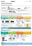
1
DVP-NS305/NS310/NS315/ NS405/NS410/NS415 RMT-D141A/D142A/D142O/D142P US Model Canadian Model SERVICE MANUAL DVP-NS315/NS415 AEP Model DVP-NS305/NS310/NS405/NS410 UK Model DVP-NS305/NS405 Russian Model Hong Kong Model Korea Model Taiwan Model Saudi Arabia Model GA Model Indian Model Pakistan Model Malaysia Model DVP-NS305 Middle East Model Oceania Model DVP-NS305/NS415 Photo : DVP-NS415 RMT-D142A PX Model Mexico Model Latin Model Argentina Model Brazilian Model DVP-NS315 SPECIFICATIONS System Laser: Semiconductor laser Signal format system: NTSC/PAL (To change the color system) Audio characteristics Frequency response: DVD VIDEO (PCM 96 kHz): 2 Hz to 44 kHz (±1.0 dB)/DVD VIDEO (PCM 48 kHz): 2 Hz to 22 kHz (±0.5 dB)/CD: 2 Hz to 20 kHz (±0.5 dB) Signal-to-noise ratio (S/N ratio): 115 dB (LINE OUT (L/R) AUDIO jacks only) Harmonic distortion: 0.003 % Dynamic range: DVD VIDEO: 103 dB/CD: 99 dB Wow and flutter: Less than detected value (±0.001% W PEAK) The signals from LINE OUT L/R (AUDIO) jacks are measured. When you play PCM sound tracks with a 96 kHz sampling frequency, the output signals from the DIGITAL OUT (OPTICAL or COAXIAL) jack are converted to 48 kHz sampling frequency. Outputs/Inputs (DVP-NS315/NS415) Outputs (DVP-NS305/NS310/NS405/NS410) (Jack name: Jack type/Output or Input level/ Load impedance) LINE IN (AUDIO)*: Phono jack/–/47 kilohms (DVP-NS315/NS415) LINE OUT (AUDIO): Phono jack/2 Vrms/ Over 10 kilohms DIGITAL OUT (OPTICAL)*: Optical output jack/–18 dBm (wave length: 660 nm) DIGITAL OUT (COAXIAL): Phono jack/ 0.5 Vp-p/75 ohms COMPONENT VIDEO OUT(Y, PB, PR): Phono jack/Y: 1.0 Vp-p/PB, PR: 0.7 Vp-p/ 75 ohms (DVP-NS315/NS415) LINE IN (VIDEO)*: Phono jack/1.0 Vp-p/ 75 ohms (DVP-NS315/NS415) LINE OUT (VIDEO): Phono jack/1.0 Vp-p/ 75 ohms S VIDEO OUT: 4-pin mini DIN/Y: 1.0 Vp-p, C: 0.286 Vp-p/75 ohms * DVP-NS405/NS410/NS415 only General Power requirements: 120 V AC, 60 Hz/ 110 to 240V AC, 50/60 Hz See page 1-1 for further information. Power consumption: 12 W/13 W See page 1-1 for further information. Dimensions (approx.): 430 × 62 × 255 mm (17 × 2 1/2 × 10 1/8 in.) (width/height/ depth) incl. projecting parts Mass (approx.): 2.3 kg (5 5/64 lb) Operating temperature: 5 ° C to 35 ° C (41 ° F to 95 ° F) Operating humidity: 25 % to 80 % Supplied accessories See page 1-3. Specifications and design are subject to change without notice. ENERGY STARR is a U.S. registered mark. As an ENERGY STARR Partner, Sony Corporation has determined that this product meets the ENERGY STARR guidelines for energy efficiency. CD/DVD PLAYER SAFETY CHECK-OUT After correcting the original service problem, perform the following safety checks before releasing the set to the customer. 1. 2. 3. 4. 5. 6. 7. Check the area of your repair for unsoldered or poorly-soldered connections. Check the entire board surface for solder splashes and bridges. Check the interboard wiring to ensure that no wires are "pinched" or contact high-wattage resistors. Look for unauthorized replacement parts, particularly transistors, that were installed during a previous repair. Point them out to the customer and recommend their replacement. Look for parts which, though functioning, show obvious signs of deterioration. Point them out to the customer and recommend their replacement. Check the line cord for cracks and abrasion. Recommend the replacement of any such line cord to the customer. Check the B+ voltage to see it is at the values specified. Check the antenna terminals, metal trim, "metallized" knobs, screws, and all other exposed metal parts for AC leakage. Check leakage as described below. 1.5 kΩ The AC leakage from any exposed metal part to earth ground and from all exposed metal parts to any exposed metal part having a return to chassis, must not exceed 0.5mA (500 microampers). Leakage current can be measured by any one of three methods. 1. 2. 3. A commercial leakage tester, such as the Simpson 229 or RCA TW-540A. Follow the manufacturers' instructions to use these instruments. A battery-operated AC milliammeter. The Data Precision 245 digital multimeter is suitable for this job. Measuring the voltage drop across a resistor by means of a VOM or battery-operated AC voltmeter. The "limit" indication is 0.75V, so analog meters must have an accurate low voltage scale. The Simpson 250 and Sanwa SH-63Trd are examples of a passive VOM that is suitable. Nearly all battery operated digital multimeters that have a 2V AC range are suitable. (See Fig. A) Unleaded solder Boards requiring use of unleaded solder are printed with the leadfree mark (LF) indicating the solder contains no lead. (Caution: Some printed circuit boards may not come printed with the lead free mark due to their particular size.) To Exposed Metal Parts on Set 0.15 µF LEAKAGE TEST AC Voltmeter (0.75 V) Earth Ground Fig. A. Using an AC voltmeter to check AC leakage. WARNING!! WHEN SERVICING, DO NOT APPROACH THE LASER EXIT WITH THE EYE TOO CLOSELY. IN CASE IT IS NECESSARY TO CONFIRM LASER BEAM EMISSION, BE SURE TO OBSERVE FROM A DISTANCE OF MORE THAN 25 cm FROM THE SURFACE OF THE OBJECTIVE LENS ON THE OPTICAL PICK-UP BLOCK. : LEAD FREE MARK Unleaded solder has the following characteristics. • Unleaded solder melts at a temperature about 40°C higher than ordinary solder. Ordinary soldering irons can be used but the iron tip has to be applied to the solder joint for a slightly longer time. Soldering irons using a temperature regulator should be set to about 350°C. Caution: The printed pattern (copper foil) may peel away if the heated tip is applied for too long, so be careful! • Strong viscosity Unleaded solder is more viscous (sticky, less prone to flow) than ordinary solder so use caution not to let solder bridges occur such as on IC pins, etc. • Usable with ordinary solder It is best to use only unleaded solder but unleaded solder may also be added to ordinary solder. CAUTION: The use of optical instrument with this product will increase eye hazard. CAUTION Use of controls or adjustments or performance of procedures other than those specified herein may result in hazardous radiation exposure. SAFETY-RELATED COMPONENT WARNING!! COMPONENTS IDENTIFIED BY MARK 0 OR DOTTED LINE WITH MARK 0 ON THE SCHEMATIC DIAGRAMS AND IN THE PARTS LIST ARE CRITICAL TO SAFE OPERATION. REPLACE THESE COMPONENTS WITH SONY PARTS WHOSE PART NUMBERS APPEAR AS SHOWN IN THIS MANUAL OR IN SUPPLEMENTS PUBLISHED BY SONY. ATTENTION AU COMPOSANT AYANT RAPPORT À LA SÉCURITÉ! LES COMPOSANTS IDENTIFÉS PAR UNE MARQUE 0 SUR LES DIAGRAMMES SCHÉMATIQUES ET LA LISTE DES PIÈCES SONT CRITIQUES POUR LA SÉCURITÉ DE FONCTIONNEMENT. NE REMPLACER CES COMPOSANTS QUE PAR DES PIÈSES SONY DONT LES NUMÉROS SONT DONNÉS DANS CE MANUEL OU DANS LES SUPPÉMENTS PUBLIÉS PAR SONY. —2— SERVICE NOTE TABLE OF CONTENTS 2. DISASSEMBLY 1. 2. DISC REMOVAL PROCEDURE (at POWER OFF) ········ 5 HOW TO SERVICE MB-103 BOARD ······························ 5 1. GENERAL Precautions ············································································· 1-1 About this Manual ································································· 1-1 This Player Can Play the Following Discs ···························· 1-1 Notes about the Discs ···························································· 1-1 Index to Parts and Controls ···················································· 1-2 Guide to On-Screen Displays (Control Bar) ························· 1-3 Simple Start Guide ···································································· 1-3 Quick Overview ····································································· 1-3 Step 1: Unpacking ································································· 1-3 Step 2: Inserting Batteries into the Remote ··························· 1-3 Step 3: TV Hookups ······························································ 1-4 Step 4: Playing a Disc ···························································· 1-4 Hookups ···················································································· 1-4 Hooking Up the Player ·························································· 1-4 Step 1: Connecting the Video Cords ····································· 1-4 Step 2: Connecting the Audio Cords ···································· 1-5 Step 3: Connecting the Power Cord ······································· 1-6 Step 4: Quick Setup ······························································· 1-6 Playing Discs ············································································· 1-6 Playing Discs ········································································· 1-6 Searching for a Particular Point on a Disc (Scan, Slow-motion Play, Search, Freeze Frame) ··············································· 1-7 Resuming Playback from the Point Where You Stopped the Disc (Resume Play/Multi-disc Resume). ···························· 1-7 Using the DVD’s Menu ························································ 1-8 Playing VIDEO CDs with PBC Functions (PBC Playback) · 1-8 Playing an MP3 Audio Track ················································ 1-8 Various Play Mode Functions (Program Play, Shuffle Play, Repeat Play, A-B Repeat Play) ··········································· 1-8 Searching for a Scene ····························································· 1-10 Searching for a Title/Chapter/Track/Index/Scene (Search mode) ·································································· 1-10 Viewing Information About the Disc ······································· 1-10 Checking the Playing Time and Remaining Time ·············· 1-10 Sound Adjustments ································································· 1-10 Changing the Sound ····························································· 1-10 TV Virtual Surround Settings (TVS) ·································· 1-11 Enjoying Movies ····································································· 1-11 Changing the Angles ··························································· 1-11 Displaying the Subtitles ······················································· 1-11 Adjusting the Picture Quality (BNR) ································· 1-12 Adjusting the Playback Picture (CUSTOM PICTURE MODE) · 1-12 Enhancing the Playback Picture (DIGITAL VIDEO ENHANCER) (DVP-NS415 only) ··································· 1-12 Using Various Additional Functions ········································ 1-12 Locking Discs (CUSTOM PARENTAL CONTROL, PARENTAL CONTROL) ················································· 1-12 Controlling Your TV with the Supplied Remote ················· 1-13 Settings and Adjustments ······················································· 1-14 Using the Setup Display. ····················································· 1-14 Setting the Display or Sound Track Language (LANGUAGE SETUP) ···················································· 1-14 Settings for the Display (SCREEN SETUP) ······················ 1-14 Custom Settings (CUSTOM SETUP) ································ 1-15 Settings for the Sound (AUDIO SETUP) ···························· 1-15 Additional Information ···························································· 1-15 Troubleshooting ·································································· 1-15 Self-diagnosis Function (When letters/numbers appear in the display) ··································································· 1-16 Glossary ·············································································· 1-16 Language Code List ····························································· 1-16 2-1. 2-2. 2-3. 2-4. 2-5. 2-6. 2-7. 2-8. 2-9. 2-10. 2-11. 2-12. UPPER CASE ································································· 2-1 FRONT PANEL ASSEMBLY and FR SUPPORT ·········· 2-1 LOADING ASSEMBLY ················································· 2-2 OPTICAL DEVICE (KHM-270AAA) ··························· 2-2 DC MOTOR and MS-81 BOARD ·································· 2-3 ER-14R BOARD ····························································· 2-3 AV-61 BOARD ································································ 2-4 MB-103 BOARD ····························································· 2-4 IF-89 BOARD ································································· 2-5 SWITCHING REGULATOR ·········································· 2-5 INTERNAL VIEWS ························································ 2-6 CIRCUIT BOARDS LOCATION ··································· 2-7 3. BLOCK DIAGRAMS 3-1. 3-2. 3-3. 3-4. 3-5. 3-6. 3-7. 3-8. 3-9. OVERALL BLOCK DIAGRAM ···································· 3-1 RF/SERVO BLOCK DIAGRAM ···································· 3-3 SIGNAL PROCESSOR BLOCK DIAGRAM ················ 3-5 SYSTEM CONTROL BLOCK DIAGRAM ··················· 3-7 VIDEO BLOCK DIAGRAM ·········································· 3-9 AUDIO BLOCK DIAGRAM ········································ 3-11 INTERFACE CONTROL BLOCK DIAGRAM ··········· 3-13 POWER BLOCK DIAGRAM (1/2) ······························ 3-15 POWER BLOCK DIAGRAM (2/2) ······························ 3-17 4. PRINTED WIRING BOARDS AND SCHEMATIC DIAGRAMS 4-1. FRAME SCHEMATIC DIAGRAM ································ 4-1 4-2. PRINTED WIRING BOARDS AND SCHEMATIC DIAGRAM ······································································ 4-4 WAVEFORMS ································································ 4-5 • IF-89 (IF COM) PRINTED WIRING BOARD ························· 4-7 • IF-89 (IF COM) SCHEMATIC DIAGRAM ······························ 4-9 • MB-103 (DVD/CD RF AMP, DIGITAL SERVO, MOTOR DRIVE, SERVO, AV DECODER, SDRAM, SYSTEM CONTROL, AUDIO DAC, PLL) PRINTED WIRING BOARD ······················· 4-11 • MB-103 (DVD/CD RF AMP, DIGITAL SERVO) (1/7) SCHEMATIC DIAGRAM ···························· 4-15 • MB-103 (MOTOR DRIVE) (2/7) SCHEMATIC DIAGRAM ···························· 4-17 • MB-103 (SERVO) (3/7) SCHEMATIC DIAGRAM ···························· 4-19 • MB-103 (AV DECODER) (4/7) SCHEMATIC DIAGRAM ···························· 4-21 • MB-103 (SDRAM) (5/7) SCHEMATIC DIAGRAM ···························· 4-23 • MB-103 (SYSTEM CONTROL) (6/7) SCHEMATIC DIAGRAM ···························· 4-25 • MB-103 (AUDIO DAC, PLL) (7/7) SCHEMATIC DIAGRAM ···························· 4-27 • AV-61 (AUDIO OUT, VIDEO OUT) PRINTED WIRING BOARD ······················· 4-29 • AV-61 (AUDIO OUT) (1/2) SCHEMATIC DIAGRAM ···························· 4-31 • AV-61 (VIDEO OUT) (2/2) SCHEMATIC DIAGRAM ···························· 4-33 • ER-14 (AV AMP) PRINTED WIRING BOARD ······················· 4-35 • ER-14 (AV AMP) SCHEMATIC DIAGRAM ···························· 4-37 • HS11S1, HS11S1F (SWITCHING REGULATOR) PRINTED WIRING BOARDS ····················· 4-39 • HS11S1, HS11S1F (SWITCHING REGULATOR) SCHEMATIC DIAGRAM ···························· 4-41 —3— 5. IC PIN FUNCTION DESCRIPTION 5-1. SYSTEM CONTROL PIN FUNCTION (MB-103 BOARD IC104: MB91307RPFV-G-BND-E1) · 5-1 6. TEST MODE 6-1. 6-2. 6-3. 6-4. 6-5. 6-6. 6-7. 6-8. 6-9. 6-10. 6-11. GENERAL DESCRIPTION ··········································· 6-1 STARTING TEST MODE ··············································· 6-1 SYSCON DIAGNOSIS ··················································· 6-1 DRIVE AUTO ADJUSTMENT ······································ 6-5 DRIVE MANUAL OPERATION ··································· 6-7 MECHA AGING ··························································· 6-11 EMERGENCY HISTORY ············································ 6-11 VERSION INFORMATION ········································· 6-11 VIDEO LEVEL ADJUSTMENT ·································· 6-11 IF CON SELF DIAGNOSTIC FUNCTION ················· 6-12 TROUBLESHOOTING ················································ 6-19 7. ELECTRICAL ADJUSTMENT 7-1. 1. 7-2. 1. 2. 3. 4. 5. 6. 7-3. POWER SUPPLY CHECK ············································· 7-1 SRV1246JUC Board ························································ 7-1 ADJUSTMENT OF VIDEO SYSTEM ··························· 7-2 Video Level Adjustment (MB-103 BOARD) ·················· 7-2 Checking S Video Output S-Y ········································· 7-2 Checking S Video Output S-C ········································· 7-2 Checking Component Video Output Y ···························· 7-2 Checking Component Video Output B-Y ························ 7-3 Checking Component Video Output R-Y ························ 7-3 ADJUSTMENT RELATED PARTS ARRANGEMENT · 7-4 8. REPAIR PARTS LIST 8-1. EXPLODED VIEWS ······················································ 8-1 8-1-1. MAIN SECTION ···························································· 8-2 8-1-2. MECHANISM DECK SECTION ··································· 8-4 8-2. ELECTRICAL PARTS LIST ·········································· 8-6 —4— SERVICE NOTE 1. 1) 2) DISC REMOVAL PROCEDURE (at POWER OFF) Insert a tapering driver into the aperture of the unit bottom, and move the lever of chuck cam in the direction of the arrow A. (See Fig. 1) Draw out the tray in the direction of the arrow B, and remove a disc. (See Fig. 1) The lever of a zipper cam Hole Tray B A Fig. 1. 2. HOW TO SERVICE MB-103 BOARD • Jig 1) 2) 3) CK-122 board (J-6090-129-A) Remove the upper case from the main unit. (Refer to 2-1) Remove the MB-103 board. (Refer to 2-7) Set the removed MB-103 board and CK-122 board to the stand as shown in Fig. 2. Stand (CK-121 board) (J-6090-132-A) 6 CK-122 board CK-120 board (J-6090-127-A) 5 Connector (CN601) 1 MB-103 board 4 Two screws (B3) Harness 6P (J-6090-126-A) Flexible flat cable five FFC 26P J-6090-117-A, FFC 9P J-6090-118-A, FFC 5P J-6090-119-A, FFC 15P J-6090-121-A, FFC 25P J-6090-122-A 3 Connector (CN101) 2 Stand Fig. 2. —5— 4) Fix the CK-120 board to the location where the MB-103 board is removed. 3 FMM-041 flexible board (CN101, 26P) 4 FMO-004 flexible board (CN103, 9P) 5 MF-128 Harness (CN109, 6P) 2 four screws (SUMIEITE(B3)+BV) 6 FMS-17 flexible board (CN105, 5P) 1 CK-120 board 7 Connector (CN113, 25P) 8 Connector (CN111, 9P) Fig. 3. 5) Set the five flexible flat cables and the harness as shown in Fig. 4 and Fig. 5. 1 Flat cable (FFC 25P :CN301(CK-122 board) 2 Flat cable (FFC 9P :CN204) 3 Flat cable (FFC 5P CN201) 2 Connector (CN114) 7 Connector (CN102) 1 Flat cable (FFC 26P :CN203) 4 Connector (CN106) 4 Harness 6P (CN110) 8 Flat cable (FFC 15P :CN202(CK-121 board)) 3 Harness 6P (CN102) 5 Connector (CN104) 6 Connector (CN112) Fig. 4. Fig. 5. —6— 6) Set complete! Fig. 6. —7— MEMO —8— DVP-NS305/NS310/NS315/NS405/NS410/NS415 SECTION 1 GENERAL This section is extracted from instruction manual. (DVP-NS315/NS415 : 3-073379-11) For the model supplied with the AC plug adaptor Precautions • The power requirements and power consumption of this player are indicated on the back of the player. Check that the player’s operating voltage is identical with your local power supply. If the AC plug of your unit does not fit into the wall autlet, attach the supplied AC plug adaptor. On operation X Power requirements and power consumption t DVP–XXXX 00V 00Hz 00W NO. 0-000-000-00 On safety • Caution – The use of optical instruments with this product will increase eye hazard. • To prevent fire or shock hazard, do not place objects filled with liquids, such as vases, on the apparatus. • Should any solid object or liquid fall into the cabinet, unplug the player and have it checked by qualified personnel before operating it any further. On power sources • The player is not disconnected from the AC power source as long as it is connected to the wall outlet, even if the player itself has been turned off. • If you are not going to use the player for a long time, be sure to disconnect the player from the wall outlet. To disconnect the AC power cord, grasp the plug itself; never pull the cord. • Should the AC power cord need to be changed, have it done at a qualified service shop only. On placement • Place the player in a location with adequate ventilation to prevent heat build-up in the player. • Do not place the player on a soft surface such as a rug that might block the ventilation holes on the bottom. • Do not place the player in a location near heat sources, or in a place subject to direct sunlight, excessive dust, or mechanical shock. • If the player is brought directly from a cold to a warm location, or is placed in a very damp room, moisture may condense on the lenses inside the player. Should this occur, the player may not operate properly. In this case, remove the disc and leave the player turned on for about half an hour until the moisture evaporates. • When you move the player, take out any discs. If you don’t, the disc may be damaged. On adjusting volume Do not turn up the volume while listening to a section with very low level inputs or no audio signals. If you do, the speakers may be damaged when a peak level section is played. On cleaning Clean the cabinet, panel, and controls with a soft cloth slightly moistened with a mild detergent solution. Do not use any type of abrasive pad, scouring powder or solvent such as alcohol or benzine. If you have any questions or problems concerning your player, please consult your nearest Sony dealer. On cleaning discs Do not use a commercially available cleaning disc. It may cause a malfunction. IMPORTANT NOTICE Caution: This player is capable of holding a still video image or on-screen display image on your television screen indefinitely. If you leave the still video image or on-screen display image displayed on your TV for an extended period of time you risk permanent damage to your television screen. Projection televisions are especially susceptible to this. 3 About this Manual Check your model name The instructions in this manual are for the 2 models: DVP-NS315 and DVP-NS415. Check your model name by looking at the front panel of the player. DVP-NS415 is the model used for illustration purposes. Any difference in operation is clearly indicated in the text, for example, “DVP-NS415 only.” • Instructions in this manual describe the controls on the remote. You can also use the controls on the player if they have the same or similar names as those on the remote. • The meaning of the icons used in this manual is described below: Icon Meaning Functions available for DVD VIDEOs or DVD-Rs/DVDRWs in video mode Functions available for VIDEO CDs or CD-Rs/CD-RWs in video CD format Functions available for DATA CDs (CD-ROMs/CD-Rs/CDRWs containing MP3* audio tracks) Functions available for music CDs or CD-Rs/CD-RWs in music CD format * MP3 (MPEG 1 Audio Layer 3) is a standard format defined by ISO/MPEG which compresses audio data. This Player Can Play the Following Discs Format of discs DVD VIDEO VIDEO CD • A disc recorded in a color system other than NTSC, such as PAL or SECAM (this player conforms to the NTSC color system). • A disc that has a non-standard shape (e.g., card, heart). • A disc with paper or stickers on it. • A disc that has the adhesive of cellophane tape or a sticker still left on it. Format of discs Music CD The “DVD VIDEO” logo is a trademark. Region code Your player has a region code printed on the back of the unit and only will play DVD VIDEO discs (playback only) labeled with identical region codes. This system is used to protect copyrights. DVDs labeled player. ALL will also play on this • Do not expose the disc to direct sunlight or heat sources such as hot air ducts, or leave it in a car parked in direct sunlight as the temperature may rise considerably inside the car. • After playing, store the disc in its case. • Clean the disc with a cleaning cloth. Wipe the disc from the center out. Note on playback operations of DVDs and VIDEO CDs Some playback operations of DVDs and VIDEO CDs may be intentionally set by software producers. Since this player plays DVDs and VIDEO CDs according to the disc contents the software producers designed, some playback features may not be available. Also, refer to the instructions supplied with the DVDs or VIDEO CDs. Region code DVP–XXXX 00V 00Hz 00W • To keep the disc clean, handle the disc by its edge. Do not touch the surface. Note Some CD-Rs, CD-RWs, DVD-Rs, or DVD-RWs (in video mode) cannot be played on this player due to the recording quality or physical condition of the disc, or the characteristics of the recording device. Furthermore, the disc will not play if it has not been correctly finalized. For more information, see the operating instructions for the recording device. Note that discs created in the Packet Write format cannot be played. If you try to play any other DVD, the message “Playback prohibited by area limitations.” will appear on the TV screen. Depending on the DVD, no region code indication may be labeled even though playing the DVD is prohibited by area restrictions. X Notes about the Discs NO. 0-000-000-00 Example of discs that the player cannot play The player cannot play the following discs: • All CD-ROMs (including PHOTO CDs)/ CD-Rs/CD-RWs other than those recorded in the following formats: –music CD format –video CD format –MP3 format that conforms to ISO9660* Level 1/Level 2, or its extended format, Joliet • Data part of CD-Extras • DVD-RWs in VR mode • DVD-ROMs • DVD Audio discs • HD layer on Super Audio CDs • Do not use solvents such as benzine, thinner, commercially available cleaners, or anti-static spray intended for vinyl LPs. Copyrights This product incorporates copyright protection technology that is protected by method claims of certain U.S. patents, other intellectual property rights owned by Macrovision Corporation, and other rights owners. Use of this copyright protection technology must be authorized by Macrovision Corporation, and is intended for home and other limited viewing uses only unless otherwise authorized by Macrovision Corporation. Reverse engineering or disassembly is prohibited. * A logical format of files and folders on CDROMs, defined by ISO (International Standard Organization). Also, the player cannot play the following discs: • A DVD with a different region code. 6 7 1-1 Front panel display Index to Parts and Controls When playing back a DVD For more information, refer to the pages indicated in parentheses. Front panel Disc type Playing status Lights up when you can change the angle (47) DVP-NS315 Lights up during Repeat Play (38) Current title/chapter or playing time (41) Current audio signal (43) When playing back a VIDEO CD with Playback Control (PBC) (32) DVP-NS415 Disc type Playing status Lights up during A-B Repeat Play (39) A [/1 (on/standby) button/indicator (27) Lights up in green when the power is on and lights up in red when the player is in standby mode. B Disc tray (27) C A (open/close) button (27) D Front panel display (9) E (remote sensor) (15) F Playback Dial (DVP-NS315) (28) (30) Multi-mode Playback Dial (DVPNS415) (28) (30) G MODE CHANGE button (DVPNS415 only) (30) H x (stop) button (28) I X (pause) button (28) J SURROUND button (44) K PICTURE MODE button (49) Current scene or playing time (41) When playing back a CD, DATA CD (MP3 audio), or VIDEO CD (without PBC) Playing status Disc type Lights up during Repeat Play (38) Current track (41) Lights up when playing MP3 audio tracks (33) Playing time (41) ,continued 8 Rear panel Remote DVP-NS315 DVP-NS315 DIGITAL OUT LINE OUT PCM/DTS/ DOLBY DIGITAL COAXIAL R-AUDIO-L COMPONENT VIDEO OUT S VIDEO OUT VIDEO A B C D E F G PB DVP-NS415 DIGITAL OUT LINE IN R-AUDIO-L VIDEO COMPONENT VIDEO OUT S VIDEO OUT Y K L M N O P Q PB PR OUT R-AUDIO-L VIDEO A DIGITAL OUT (COAXIAL) jack (22) (23) (24) B DIGITAL OUT (OPTICAL) jack (DVP-NS415 only) (22) (23) (24) C LINE IN L/R (AUDIO) jacks (DVPNS415 only) (16) (18) D LINE IN (VIDEO) jack (DVP-NS415 only) (16) (18) Z OPEN/CLOSE button (28) SUR (surround) button (44) SUBTITLE button (47) AUDIO button (43) ANGLE button (47) CLEAR button (35) ./> PREV/NEXT (previous/ next) buttons (28) H m/M SCAN/SLOW buttons (29) I X PAUSE button (28) J H PLAY button (27) Y PR PCM/DTS/ DOLBY DIGITAL COAXIAL OPTICAL 9 E S VIDEO OUT jack (18) F COMPONENT VIDEO OUT jacks (18) G LINE OUT (VIDEO) jack (18) H LINE OUT L/R (AUDIO) jacks (21) (22) (23) R S T U V W X The H button has a tactile dot.* C/X/x/c buttons (32) DISPLAY button (13) TOP MENU button (32) TV [/1 (on/standby) button (55) [/1 (on/standby) button (27) PICTURE MODE button (49) VOL (volume) +/– buttons (55) The + button has a tactile dot.* TV/VIDEO button (55) SEARCH MODE button (40) REPLAY button (28) x STOP button (28) ENTER button (25) O RETURN button (32) MENU button (32) (33) * Use the tactile dot as a reference when operating the player. ,continued 10 1-2 11 DVP-NS415 A TV [/1 (on/standby) button (55) B Z OPEN/CLOSE button (28) C Number buttons (32) D E F G Guide to On-Screen Displays (Control Bar) The number 5 button has a tactile dot.* CLEAR button (35) SUBTITLE button (47) AUDIO button (43) ./> PREV/NEXT (previous/ next) buttons (28) H m/M SCAN/SLOW buttons (29) I X PAUSE button (28) J H PLAY button (27) K L M N O The following explains the Control Bar. The Control Bar is used for making adjustments to the settings or displaying information during playback. The displayed contents differ according to the type of disc being played. The numbers in parentheses indicate reference pages. Displaying the Control Bar during playback The H button has a tactile dot.* C/X/x/c buttons (32) DISPLAY button (13) TOP MENU button (32) [/1 (on/standby) button (27) VOL (volume) +/– buttons (55) The following displays appear when the DISPLAY button is pressed repeatedly during playback. You can select the setting that suits the current playback item and view the related information. ◆Display 1 The following play modes 1~4 can be set. The indicator lights up in blue when activated. Example: When Repeat Play is selected. (The display will differ when A-B Repeat Play is set.) The + button has a tactile dot.* P TV/VIDEO button (55) Q ENTER button (performs the same function as Z) R PICTURE MODE button (49) S ANGLE button (47) T SUR (surround) button (44) U TIME/TEXT button (41) V REPEAT button (38) W REPLAY button (28) X SEARCH MODE button (40) Y x STOP button (28) Z ENTER button (25) wj O RETURN button (32) wk MENU button (32) (33) CHAPTER G H I J TVS (44) “BNR” (48) “CUSTOM PICTURE MODE” (49) “DIGITAL VIDEO ENHANCER” (50) (DVP-NS415 only) m ◆Display 3 The following playback information is displayed. Example: When playing a DVD. T41 – 8 K L M N T 1:01:57 TIME/TEXT icon Title number of the DVD (40) Chapter number of the DVD (40) Playing time or remaining time (41) m ◆Display 4 (DVD playback only) A B C D E F * Use the tactile dot as a reference when operating the player. Repeat Play (38) Shuffle Play (37) Program Play (35) A-B Repeat Play (39) Unit being repeated in this example. Playback status (NPlayback, XPause, xStop, etc.) m ◆Display 2 The following play modes 7~0 can be set. The indicator lights up in blue when activated. Example: When “TVS” is set. DOLBY DIGITAL 3 / 2 .1 O Format of the current audio signal (43) m ◆No display m ◆Return to Display 1 ,continued 12 Displaying the Control Bar in stop mode ◆Display 3 Shows the same information as Display 2 during playback. ◆Display 1 The following settings can be made. Simple Start Guide Quick Overview A quick overview presented in this guide will give you enough information to start using the player for your enjoyment. To use the surround sound features of this player, refer to “Hookups” on page 18. m ◆Display 4 Shows the same information as Display 3 during playback. A B • You cannot connect this player to a TV that does not have a video input jack. • Be sure to disconnect the power of each component before connecting. T 1:01:57 m SETUP (57) • Select QUICK to make the minimum number of basic adjustments for using the player. • Select CUSTOM to make a full range of adjustments. • Select RESET to return the SETUP adjustments to the default settings. You can control the player using the supplied remote. Insert two Size AA (R6) batteries by matching the 3 and # ends on the batteries to the markings inside the compartment. When using the remote, point it at the remote sensor on the player. Notes QUICK T41 – 8 Step 2: Inserting Batteries into the Remote Simple Start Guide The following displays appear when the DISPLAY button is repeatedly pressed during stop mode. You can make basic adjustments and customize the player to suit your viewing preferences. 13 Step 1: Unpacking ◆No display m Check that you have the following items: • Audio/video cord (pinplug × 3 y pinplug × 3) (1) • Remote commander (remote) (1) • Size AA (R6) batteries (2) • A plug adapter is included with some models. ◆Return to Display 1 PARENTAL CONTROL (51) • Set this to limit the playback of selected discs on this player. m ◆Display 2 Shows the same information as Display 1 during playback. Notes • Do not leave the remote in an extremely hot or humid place. • Do not drop any foreign object into the remote casing, particularly when replacing the batteries. • Do not expose the remote sensor to direct light from the sun or a lighting apparatus. Doing so may cause a malfunction. • If you do not use the remote for an extended period of time, remove the batteries to avoid possible damage from battery leakage and corrosion. CHAPTER m 14 15 1-3 Step 3: TV Hookups Step 4: Playing a Disc Connect the supplied audio/video cord and the power cord in the order (1~3) shown below. Be sure to connect the power cord last. Simple Start Guide If you are connecting to a VCR and your TV has only one available input jack* (DVP-NS415 only) to LINE IN (VIDEO) to LINE IN L/R (AUDIO) to video output to audio output LINE IN R-AUDIO-L With the playback side facing down VCR VIDEO IN CD/DVD Player OUT OUT R-AUDIO-L DIGITAL OUT VIDEO PCM/DTS/ DOLBY DIGITAL COAXIAL OPTICAL LINE R-AUDIO-L VIDEO OUT R-AUDIO-L VIDEO IN COMPONENT VIDEO OUT S VIDEO OUT Y to LINE OUT (VIDEO) to video input 3 Power source TV INPUT E Place the disc on the tray with the playback side facing down. L (supplied) AUDIO F Press H. R to audio input * If you are connecting a VCR and your TV has only one available input jack (DVP-NS415 only) If your TV has only one available input jack, connect your VCR or similar device to the LINE IN jacks on the player. In order to view the pictures from your VCR, the DVD player must be in standby mode. Note that the DVD player will only pass signals through the LINE jacks and will not output the VCR signals from any other jack. If your TV has more than one available input jack, connect your VCR directly to your TV. Depending on the disc, a menu may be displayed on the TV screen. If so, select the item you want from the menu and play the DVD (page 32) or VIDEO CD disc (page 32). D Press A on the player to open the disc tray. VIDEO 1 Audio/video cord After Step 6 B Press [/1 on the player. C Switch the input selector on your TV so that the signal from the player appears on the TV screen. PB PR to LINE OUT L/R (AUDIO) A Turn on the TV. To stop playing Press x. To remove the disc Press A. To turn off the player Press [/1. The player enters standby mode and the power indicator lights up in red. The disc tray closes and the player begins playing the disc. 2 Power source When connecting to a wide screen TV Depending on the disc, the image may not fit your TV screen. If you want to change the aspect ratio, please refer to page 59. When connecting to a monaural TV Use a stereo-mono conversion cord (not supplied). Connect the LINE OUT (VIDEO) jack on the player to the TV’s video input jack, and connect the LINE OUT L/R (AUDIO) jacks to the TV’s audio input jack. 16 17 A If you are connecting to a video input jack Hookups Connect the yellow plug of the audio/video cord (supplied) to the yellow (video) jacks. You will enjoy standard quality images. Hooking Up the Player Yellow (Video) White (L) Yellow (Video) Red (R) Red (R) White (L) Hookups Follow Steps 1 to 4 to hook up and adjust the settings of the player. Before you start, disconnect the power cords, check that you have all of the supplied accessories, and insert the batteries into the remote (page 15). Use the red and white plugs to connect to the audio input jacks (page 21). (Do this if you are connecting to a TV only.) Notes • Plug cords securely to prevent unwanted noise. • Refer to the instructions supplied with the components to be connected. B If you are connecting to an S VIDEO input jack Connect an S VIDEO cord (not supplied). You will enjoy high quality images. Step 1: Connecting the Video Cords Connect this player to your TV monitor, projector, or AV amplifier (receiver) using a video cord. Select one of the patterns A through C, according to the input jack on your TV monitor, projector, or AV amplifier (receiver). A C If you are connecting to a monitor, projector, or AV amplifier (receiver) having component video input jacks (Y, PB, PR) Connect the component via the COMPONENT VIDEO OUT jacks using a component video cord (not supplied) or three video cords (not supplied) of the same kind and length. You will enjoy accurate color reproduction and high quality images. C INPUT VIDEO (yellow) Audio/video cord (supplied) Component video cord (not supplied) COMPONENT VIDEO IN Y (green) PB (blue) L PR AUDIO R Green Blue Blue Red Red (red) TV, projector or AV amplifier (receiver) TV, projector or AV amplifier (receiver) Green Notes • Connect the player directly to the TV. If you pass the player signals via the VCR, you may not receive a clear image on the TV screen. VCR (yellow) (green) (blue) to LINE OUT (VIDEO) DIGITAL OUT PCM/DTS/ DOLBY DIGITAL COAXIAL OPTICAL LINE IN R-AUDIO-L VIDEO (red) CD/DVD player COMPONENT VIDEO OUT S VIDEO OUT CD/DVD player TV Connect directly Y PB PR OUT R-AUDIO-L VIDEO • If your TV has only one available audio/video input jack, connect the VCR to the LINE IN jacks on the player (DVP-NS415 only). In order to view the pictures from your VCR, the DVD player must be in standby mode (page 16). INPUT S VIDEO VCR S VIDEO cord (not supplied) TV, projector or AV amplifier (receiver) CD/DVD player TV B l : Signal flow 18 19 1-4 Connecting to your TV A Step 2: Connecting the Audio Cords This connection will use your TV speakers for sound. Refer to the chart below to select the connection that best suits your system. Be sure to also read the instructions for the components you wish to connect. CD/DVD player DIGITAL OUT LINE VIDEO VIDEO COMPONENT VIDEO OUT S VIDEO OUT Y PB Hookups R-AUDIO-L OUT R-AUDIO-L IN PCM/DTS/ DOLBY DIGITAL COAXIAL OPTICAL PR Select a connection Select one of the following connections, A through D . A Components to be connected Connection TV A (page 21) Stereo amplifier (receiver) (having L and R audio input jacks only, or having a digital input jack) • 2 speakers (front L and R) B (page 22) MD deck/DAT deck B (page 22) AV amplifier (receiver) with a Dolby* Surround (Pro Logic) decoder (having L and R audio input jacks only, or having a digital input jack) • 3 speakers (front L and R, and rear (monaural)) or • 6 speakers (front L and R, center, rear L and R, subwoofer) C (page 23) AV amplifier (receiver) having a Dolby Digital or DTS** decoder and a digital input jack • 6 speakers (front L and R, center, rear L and R, subwoofer) D LINE R-AUDIO-L VIDEO OUT R-AUDIO-L VIDEO IN (yellow)* (yellow) (white) (white) (red) Audio/video cord (supplied) to LINE OUT L/R (AUDIO) TV (red) to audio input l : Signal flow * The yellow plug is used for video signals (page 18). ◆Recommended surround sound effects for this connection • TVS DYNAMIC (page 45) • TVS WIDE (page 45) (page 24) z Hint When connecting to a monaural TV, use a stereomono conversion cord (not supplied). Connect the LINE OUT L/R (AUDIO) jacks to the TV’s audio input jack. * Manufactured under license from Dolby Laboratories. “Dolby,” “Pro Logic,” and the double-D symbol are trademarks of Dolby Laboratories. ** “DTS” and “DTS Digital Out” are trademarks of Digital Theater Systems, Inc. ,continued 20 C Connecting to an AV amplifier (receiver) having a Dolby Surround (Pro Logic) decoder and 3 to 6 speakers If the stereo amplifier (receiver) has audio input jacks L and R only, use B-1 . If the amplifier (receiver) has a digital input jack, or when connecting to an MD deck or DAT deck, use B-2 . In this case, you can also connect the player directly to the MD deck or DAT deck without using your stereo amplifier (receiver). You can enjoy the Dolby Surround effects only when playing Dolby Surround audio or multichannel audio (Dolby Digital) discs. If your amplifier (receiver) has L and R audio input jacks only, use C-1 . If your amplifier (receiver) has a digital input jack, use C-2 . CD/DVD player DIGITAL OUT PCM/DTS/ DOLBY DIGITAL COAXIAL OPTICAL LINE IN R-AUDIO-L VIDEO CD/DVD player COMPONENT VIDEO OUT S VIDEO OUT Y DIGITAL OUT PB PCM/DTS/ DOLBY DIGITAL COAXIAL OPTICAL LINE IN R-AUDIO-L VIDEO OUT R-AUDIO-L VIDEO COMPONENT VIDEO OUT S VIDEO OUT PR OUT R-AUDIO-L B-2 DIGITAL OUT B-1 Coaxial digital cord (not supplied) C-2 DIGITAL OUT Stereo audio cord (not supplied) (white) PCM/DTS/ DOLBY DIGITAL COAXIAL OPTICAL LINE IN R-AUDIO-L Stereo audio cord (not supplied) (white) PCM/DTS/ DOLBY DIGITAL COAXIAL OPTICAL VIDEO LINE IN R-AUDIO-L VIDEO OUT R-AUDIO-L VIDEO or (red) OUT R-AUDIO-L or VIDEO (red) to DIGITAL OUT (COAXIAL or OPTICAL) to LINE OUT L/R (AUDIO) Optical digital cord (not supplied) Remove jack cap before connecting (DVP-NS415 only) C-1 Coaxial digital cord (not supplied) or to DIGITAL OUT (COAXIAL or OPTICAL) (white) Optical digital cord (not supplied) Remove jack cap before connecting (DVP-NS415 only) (red) to coaxial or optical digital input [Speakers] Y PB PR VIDEO or Hookups B Connecting to a stereo amplifier (receiver) and 2 speakers/Connecting to an MD deck or DAT deck 21 to audio input to LINE OUT L/R (AUDIO) (white) (red) to audio input to coaxial or optical digital input [Speakers] [Speakers] Amplifier (receiver) with Dolby Surround decoder Stereo amplifier (receiver) Front (L) MD deck/DAT deck Rear (L) Front (L) Rear (R) Front (R) Front (R) l: Signal flow l: Signal flow ◆Recommended surround sound effects for the B-1 connection only • TVS STANDARD (page 45) z Hint In connection B-1 , you can use the supplied audio/video cord instead of using a separate audio cord. Subwoofer Center Rear (mono) Note Note When connecting 6 speakers, replace the monaural rear speaker with a center speaker, 2 rear speakers and a subwoofer. If you select one of the TVS effects (page 44) while playing a disc, no sound will come from your speakers with the B-2 connection. ,continued 22 1-5 23 D Connecting to an AV amplifier (receiver) with a digital input jack having a Dolby Digital or DTS decoder and 6 speakers Step 3: Connecting the Power Cord This connection will allow you to use the Dolby Digital or DTS decoder function of your AV amplifier (receiver). You are not able to enjoy the surround sound effects of this player. Plug the player and TV power cords into an AC outlet. DIGITAL OUT LINE R-AUDIO-L VIDEO OUT R-AUDIO-L VIDEO IN PCM/DTS/ DOLBY DIGITAL COAXIAL OPTICAL COMPONENT VIDEO OUT S VIDEO OUT Hookups CD/DVD player Step 4: Quick Setup Y PB PR Follow the steps below to make the minimum number of basic adjustments for using the player. To skip an adjustment, press >. To return to the previous adjustment, press .. DVP-NS315 D DVP-NS415 DIGITAL OUT LANGUAGE SETUP OSD: MENU: AUDIO: SUBTITLE: PCM/DTS/ DOLBY DIGITAL COAXIAL OPTICAL 5 Press X/x to select a language. to DIGITAL OUT (COAXIAL or OPTICAL) The player uses the language selected here to display the menu and subtitles as well. ENTER or Coaxial digital cord (not supplied) Rear (L) 6 Press ENTER. Optical digital cord (not supplied) Remove jack cap before connecting (DVP-NS415 only) to coaxial digital input [Speakers] ENGLISH ENGLISH FRENCH SPANISH PORTUGUESE 1 Turn on the TV. 2 Press [/1. 3 Switch the input selector on your to optical digital input Subwoofer Front (L) Rear (R) SCREEN SETUP TV TYPE: SCREEN SAVER: BACKGROUND: 4:3 LETTER BOX 4:3 LETTER BOX 4:3 PAN SCAN 16:9 TV so that the signal from the player appears on the TV screen. [Speakers] AV amplifier (receiver) having a decoder The Setup Display for selecting the aspect ratio of the TV to be connected appears. “Press [ENTER] to run QUICK SETUP” appears at the bottom of the screen. If this message does not appear, select “QUICK” under “SETUP” in the Control Bar to run Quick Setup (page 58). Center 4 Press ENTER without inserting a Front (R) l: Signal flow disc. Note The Setup Display for selecting the language used in the on-screen display appears. After you have completed the connection, be sure to set “DOLBY DIGITAL” to “DOLBY DIGITAL” and “DTS” to “ON” (page 25) in Quick Setup. Otherwise, no sound or a loud noise will come from the speakers. 7 Press X/x to select the setting that matches your TV type. ◆ If you have a 4:3 standard TV • 4:3 LETTER BOX or 4:3 PAN SCAN (page 59) ◆ If you have a wide-screen TV or a 4:3 standard TV with a wide-screen mode • 16:9 (page 59) 8 Press ENTER. The Setup Display for selecting the type of jack used to connect your amplifier (receiver) appears. ,continued 24 4 Press A on the player, and place a “DTS” is selected. Is this player connected to an amplifier (receiver) ? Select the type of jack you are using. AUDIO SETUP AUDIO ATT: OFF AUDIO DRC: STANDARD DOWNMIX: DOLBY SURROUND DIGITAL OUT: ON D-PCM DOLBY DIGITAL: DTS: OFF OFF ON YES LINE OUTPUT L/R (AUDIO) DIGITAL OUTPUT NO 9 Press X/x to select the type of jack B-2 B-2 Choose the signal that matches the audio connection you selected on pages 22 to 24 ( B through D ). AUDIO SETUP AUDIO ATT: OFF AUDIO DRC: STANDARD DOWNMIX: DOLBY SURROUND DIGITAL OUT: ON D-PCM DOLBY DIGITAL: D-PCM DTS: DOLBY DIGITAL MODE CHANGE (DVP-NS415 only) DVP-NS315 B-2 C-2 D • DOLBY DIGITAL (only if the amplifier (receiver) has a Dolby Digital decoder) (page 62) Press [/1. The player enters standby mode. Enjoying the surround sound effects AUDIO To enjoy the surround sound effects of this player or your amplifier (receiver), set the following items as described below for the audio connection you selected on pages 22 to 24 ( B through D ). Each of these is the default setting and does not need to be adjusted when you first connect the player. Refer to page 57 for using the Setup Display. 1 Turn on your TV. 2 Press [/1. A The player turns on and the power indicator lights up in green. 11Press ENTER. C-1 3 Switch the input selector on your • Set “DOWNMIX” to “DOLBY SURROUND” (page 61) • If the sound distorts even when the volume is turned down, set “AUDIO ATT” to “ON” (page 61) C-2 z Hint You can have the player turn off automatically whenever you leave it in stop mode for more than 30 minutes. To turn on this function, set “AUTO POWER OFF” in “CUSTOM SETUP” to “ON” (page 60). Notes on playing DTS sound tracks on a CD Audio Connection (pages 21 to 24) B-2 The disc tray closes, and the player starts playback (continuous play). Adjust the volume on the TV or the amplifier (receiver). Depending on the disc, a menu may appear on the TV screen. For DVDs, see page 32. For VIDEO CDs, see page 32. To turn off the player Quick Setup is finished. All connections and setup operations are complete. B-1 With the playback side facing down 5 Press H. DVP-NS415 13Press ENTER. • No additional settings are needed. • D-PCM (page 62) H/Playback Dial C-2 • ON (only if the amplifier (receiver) has a DTS decoder) (page 62) • Select “DIGITAL OUTPUT.” The Setup Display for “DOLBY DIGITAL” appears. Dolby Digital signal you wish to send to your amplifier (receiver). A D D 10Press X/x to select the type of Power [/1 indicator • OFF (page 62) C-1 C-2 Refer to the operating instructions supplied with your disc. Choose the item that matches the audio connection you selected on pages 22 to 24 ( B through D ). A • Select “LINE OUTPUT L/R (AUDIO).” Quick Setup is finished and connections are complete. Depending on the DVD or VIDEO CD, some operations may be different or restricted. not you wish to send a DTS signal to your amplifier (receiver). • If you connect just a TV and nothing else, select “NO.” Quick Setup is finished and connections are complete. B-1 Playing Discs 12Press X/x to select whether or Choose the item that matches the audio connection you selected on pages 21 to 24 ( A through D ). disc on the disc tray. Playing Discs Playing Discs (if any) you are using to connect to an amplifier (receiver), then press ENTER. 25 TV so that the signal from the player appears on the TV screen. ◆ When using an amplifier (receiver) Turn on the amplifier (receiver) and select the appropriate channel so that you can hear sound from the player. D • Set “DOWNMIX” to “DOLBY SURROUND” (page 61) • Set “DIGITAL OUT” to “ON” (page 61) • When playing DTS-encoded CDs, excessive noise will be heard from the analog stereo jacks. To avoid possible damage to the audio system, the consumer should take proper precautions when the analog stereo jacks of the player are connected to an amplification system. To enjoy DTS Digital Surround™ playback, an external 5.1-channel decoder system must be connected to the digital jack of the player. • Set the sound to “STEREO” using the AUDIO button when you play DTS sound tracks on a CD (page 43). • Do not play DTS sound tracks without first connecting the player to an audio component having a built-in DTS decoder. The player outputs the DTS signal via the DIGITAL OUT (COAXIAL or OPTICAL) jack even if “DTS” in “AUDIO SETUP” is set to “OFF” in the Setup Display (page 62), ,continued 26 1-6 27 and may affect your ears or cause your speakers to be damaged. Notes on playing DVDs with a DTS sound track Additional operations DVP-NS315 DVP-NS415 Operation Replay the previous scene (DVD only) Press REPLAY Note Even if you select “RESET” under “SETUP” in the Control Bar (page 58), the disc tray remains locked. * Operable when the MODE CHANGE indicator lights up in green or turns off. For more details about the Multi-mode Playback Dial, see page 30 (DVP-NS415 only). Searching for a Particular Point on a Disc (Scan, Slow-motion Play, Search, Freeze Frame) z Hint The Replay function is useful when you want to review a scene or dialog that you missed. You can quickly locate a particular point on a disc by monitoring the picture or playing back slowly. Note DVP-NS315 DVP-NS415 Playing Discs • DTS audio signals are output only through the DIGITAL OUT (COAXIAL or OPTICAL) jack. • When you play a DVD with DTS sound tracks, set “DTS” to “ON” in “AUDIO SETUP” (page 62). • If you connect the player to audio equipment without a DTS decoder, do not set “DTS” to “ON” in “AUDIO SETUP” (page 62). A loud noise may come out from the speakers, affecting your ears or causing the speakers to be damaged. To You may not be able to use the Replay function with some scenes. Locking the disc tray (Child Lock) You can lock the disc tray to prevent children from opening it. DVP-NS315 DVP-NS415 REPLAY Playback Dial (DVP-NS315) Multi-mode Playback Dial (DVP-NS415) ENTER MODE CHANGE (DVP-NS415 only) To Operation Stop Press x Pause Press X Resume play after pause Press X or H Go to the next chapter, Press > on the track, or scene in remote, or briefly turn continuous play mode the Playback Dial* on the player clockwise Go back to the previous chapter, track, or scene in continuous play mode Press . on the remote, or briefly turn the Playback Dial* on the player counterclockwise Stop play and remove Press Z the disc RETURN Note Depending on the DVD/VIDEO CD, you may not be able to do some of the operations described. When the player is in standby mode, press O RETURN, ENTER, and then [/1 on the remote. Locating a point quickly by playing a disc in fast forward or fast reverse (Scan) The player turns on and “LOCKED” appears on the front panel display. The Z button on the player or the remote does not work while the Child Lock is set. Press m or M while playing a disc. When you find the point you want, press H to return to normal speed. Each time you press m or M during scan, the playback speed changes. Three speeds are available. With each press the indication changes as follows: To unlock the disc tray When the player is in standby mode, press O RETURN, ENTER, and then [/1 again. ,continued 28 Playback direction × 2B (DVD/CD only) t 1M t 2M Opposite direction × 2b (DVD only) t 1m t 2m Watching frame by frame (Slowmotion play) Press m or M when the player is in pause mode. To return to the normal speed, press H. Each time you press m or M during Slow-motion play, the playback speed changes. Two speeds are available. With each press the indication changes as follows: Playback direction 2 y1 Opposite direction (DVD only) 2 y1 The “2 y”/“2 than “1 y”/“1 Resuming Playback from the Point Where You Stopped the Disc (Resume You can search for a particular point on a disc in various ways using the MODE CHANGE button. Play/Multi-disc Resume) To go to the next chapter/track/scene The player remembers the point where you stopped the disc. During playback and with the MODE CHANGE indicator turned off, briefly turn the Multi-mode Playback Dial clockwise to skip to the next chapter/track/scene, or counterclockwise to skip to the previous ones. (The same operation can be made when the MODE CHANGE indicator lights up in green.) DVP-NS315 Storing the point where you stopped the disc (Multi-disc Resume) (DVP-NS415 only) To locate a point quickly (Search) During playback and with the MODE CHANGE indicator turned off, turn and hold the Multi-mode Playback Dial clockwise to locate a point in the playback direction, counterclockwise to locate a point in the opposite direction. When you find the point you want, release the dial to return to normal playback speed. Resuming playback for the current disc (Resume Play) To locate a specific title/chapter/track ” playback speed is slower .” Using the Playback Dial on the player (DVP-NS315 only) You can search for a particular point on a disc in various ways using the Playback Dial. To go to the next chapter/track/scene During playback, briefly turn the Playback Dial clockwise to skip to the next chapter/ track/scene, or counterclockwise to skip to the previous ones. To locate a point quickly (Search) During playback, turn and hold the Playback Dial clockwise to locate a point in the playback direction, or counterclockwise to locate a point in the opposite direction. When you find the point you want, release the dial to return to normal playback speed. DVP-NS415 1 Press MODE CHANGE repeatedly so that the indicator lights up in green. 2 During playback, turn and hold the Multi-mode Playback Dial clockwise to locate succeeding titles/chapters/tracks, or counterclockwise to locate preceding ones. The player remembers the point where you stopped the disc even if the player enters standby mode by pressing [/1. 1 Press MODE CHANGE repeatedly so that the indicator lights up in amber. 2 During playback, turn the Multi-mode Playback Dial clockwise to go to the next frame, or counterclockwise to go to the previous frame. If you turn and hold the dial, you can view the frames in succession. While playing a disc, press x to stop playback. “RESUME” appears on the front panel display. To play one frame at a time (Freeze Frame) 1 Notes • The point where you stopped playing is cleared when: – you change the play mode. – you change the settings on the Setup Display. – you open the disc tray (DVP-NS315 only). – you disconnect the power cord. • When playing a CD, the point where you stopped is cleared when the disc tray is opened or the power cord is disconnected. • When playing a DATA CD, the point where you stopped playing is cleared when the player enters standby mode, the disc tray is opened, or the power cord is disconnected. • This function may not work with some discs. Playing Discs The “× 2B”/“× 2b” playback speed is about twice the normal speed. The “2M”/“2m” playback speed is faster than “1M”/ “1m.” Using the Multi-mode Playback Dial on the player (DVP-NS415 only) 29 2 Press H. The player starts playback from the point where you stopped the disc in Step 1. z Hint To play from the beginning of the disc, press x twice, then press H. 30 The player stores the point where you stopped the disc and resumes playback from the same point the next time you insert the same disc. Resume playback points for up to 6 different DVD/VIDEO discs remain in memory even if you disconnect the power cord. When you store a resume playback point for the seventh disc, the resume playback point for the first disc is deleted. z Hints • To play from the beginning of the disc, press x twice, then press H. • To turn off the Multi-disc Resume function, set “MULTI-DISC RESUME” in “CUSTOM SETUP” to “OFF” (page 60). Playback restarts at the resume point only for the current disc in the player. Notes • The point where you stopped playing is cleared when: – you change the play mode. – you change the settings on the Setup Display. • This function may not work with some discs. 31 1-7 To return to the menu Using the DVD’s Menu DVP-NS315 Press O RETURN. z Hint To play without using PBC, press ./> while the player is stopped to select a track, then press H or ENTER. “Play without PBC” appears on the TV screen and the player starts continuous play. You cannot play still pictures such as a menu. To return to PBC playback, press x twice then press H. PBC (Playback Control) allows you to play VIDEO CDs interactively by following the menu on the TV screen. DVP-NS315 DVP-NS415 Playing an MP3 Audio Track You can play back DATA CDs (CD-ROMs/ CD-Rs/CD-RWs) recorded in MP3 (MPEG1 Audio Layer 3) format. DVP-NS315 DVP-NS415 Note DVP-NS415 Playing Discs A DVD is divided into long sections of a picture or a music feature called “titles.” When you play a DVD which contains several titles, you can select the title you want using the TOP MENU button. When you play DVDs that allow you to select items such as the language for the subtitles and the language for the sound, select these items using the MENU button. Playing VIDEO CDs with PBC Functions (PBC Playback) Depending on the VIDEO CD, “Press ENTER” in Step 3 may appear as “Press SELECT” in the instructions supplied with the disc. In this case, press H. Number buttons Number buttons ENTER ENTER RETURN MENU ENTER RETURN MENU TOP MENU 1 Press Z and place a DATA CD on 1 Start playing a VIDEO CD with PBC the disc tray. functions. 1 Press TOP MENU or MENU. The disc’s menu appears on the TV screen. The contents of the menu vary from disc to disc. 2 Press C/X/x/c to select the item you want to play or change. You can also use the number buttons to select the item. (DVP-NS415 only) 3 Press ENTER. 2 Press H. The menu for your selection appears. The disc tray closes, and the player starts to play the first MP3 audio track in the first album on the disc. 2 Select the item number you want by pressing X/x. You can also use the number buttons to select the item number and track. (DVPNS415 only) Notes • This player can play MP3 audio tracks recorded in the following sampling frequencies: 32kHz, 44.1kHz, 48kHz. • The playback order may be different from the edited order. See “The Playback order of MP3 audio tracks” below for details. 3 Press ENTER. 4 Follow the instructions in the menu for interactive operations. Selecting an album and track Refer to the instructions supplied with the disc, as the operating procedure may differ depending on the VIDEO CD. 1 Press MENU. The list of MP3 albums recorded on the DATA CD appears. ,continued 32 1( 30) ROCK BEST HIT KARAOKE JAZZ R&B MY FAVORITE SONGS CLASSICAL SALSA OF CUBA BOSSANOVA Select an album using X/x and press ENTER. The list of tracks contained in the album appears. JAZZ 1(90) 0 0 0 0 0 0 0 3 1 2 3 4 5 6 7 SHE IS SPECIAL ALL YOU NEED IS ... SPICY LIFE HAPPY HOUR RIVER SIDE 5 TAKE TIME,TAKE TIME Select a track using X/x and press ENTER. The selected track starts playing. When a track or album is being played, its title is shaded. To play a Multi Session CD This player can play Multi Session CDs when an MP3 audio track is located in the first session. Any subsequent MP3 audio tracks, recorded in the later sessions, can also be played back. When audio tracks and images in music CD format or video CD format are recorded in the first session, only the first session will be played back. • If you put the extension “.MP3” to data not in MP3 format, the player cannot recognize the data properly and will generate a loud noise which could damage your speaker system. • The player cannot play audio tracks in MP3PRO format. Notes • Depending on the software you use to create the DATA CD, the playback order may differ from the illustration above. • The playback order above may not be applicable if there are more than a total of 200 albums and tracks in the DATA CD. • The player can recognize up to 100 albums (the player will count just albums, including albums that do not contain MP3 audio tracks). The player will not play any albums beyond the first 100 albums. Of the first 100 albums, the player will play no more than a combined total of 200 albums and tracks. The Playback order of MP3 audio tracks The playback order of albums and tracks recorded on a DATA CD is as follows. ◆Structure of disc contents Tree 1 To go to the next or previous page z Hints • If you add numbers (01, 02, 03, etc.) to the front of the track file names, the tracks will be played in that order. • Since a disc with many trees takes longer to start playback, place your albums within the first two trees. Notes Tree 2 Tree 3 Tree 4 Tree 5 ROOT Press c or C. To return to the previous display Press O RETURN. Various Play Mode Functions (Program Play, Shuffle Play, Repeat Play, A-B Repeat Play) You can set the following play modes: • Program Play (page 35) • Shuffle Play (page 37) • Repeat Play (page 38) • A-B Repeat Play (page 39) Playing Discs 2 When you insert a DATA CD and press H, the numbered tracks are played sequentially, from 1 through 7. Any sub-albums/tracks contained within a currently selected album take priority over the next album in the same tree. (Example: C contains D so 4 is played before 5.) When you press MENU and the list of MP3 albums appears (page 33), the albums are arranged in the following order: A t B t C t D t F t G. Albums that do not contain tracks (such as album E) do not appear in the list. See the instructions of the CD-R/RW device or recording software (not supplied) for details on the recording format. 33 Note The play mode is canceled when: – you open the disc tray. – the player enters standby mode by pressing [/1. Creating your own program (Program Play) You can play the contents of a disc in the order you want by arranging the order of the titles, chapters, or tracks on the disc to create your own program. You can program up to 99 titles, chapters, and tracks. DVP-NS315 DVP-NS415 Number buttons CLEAR To turn off the display Press MENU. Notes ENTER • Only the letters in the alphabet and numbers can be used for album or track names. Anything else is displayed as an asterisk. • ID3 tags cannot be displayed. DISPLAY About MP3 audio tracks You can play MP3 audio tracks on CDROMs, CD-Rs, or CD-RWs. However, the discs must be recorded according to ISO9660 level 1, level 2, or Joliet format for the player to recognize the tracks. You can also play discs recorded in Multi Session. album track ,continued 34 1-8 35 1 Press DISPLAY twice while the player is in stop mode. ALL CLEAR 1. TITLE – – 2. TITLE – – 3. TITLE – – 4. TITLE – – 5. TITLE – – 6. TITLE – – 7. TITLE – – “TRACK” is displayed when you play a VIDEO CD or CD. PROGRAM –– 01 02 03 04 05 Titles or tracks recorded on a disc 3 Press DISPLAY repeatedly until the display is turned off. –– 01 02 03 04 05 ◆ When playing a VIDEO CD or CD For example, select track “02.” Press X/x to select “02” under “T,” then press ENTER. The cursor moves to the title or track row “T” (in this case, “01”). T C –– 01 02 03 04 05 ALL 01 02 03 04 05 06 0:15:30 T PROGRAM ALL CLEAR 1. TRACK 2. TRACK 3. TRACK 4. TRACK 5. TRACK 6. TRACK 7. TRACK 02 –– –– –– –– –– –– –– 01 02 03 04 05 ◆ When playing a DVD For example, select chapter “03” of title “02.” Press X/x to select “02” under “T,” then press ENTER. You can also use the number buttons to select the number (DVP-NS415 only). 5 Select the program number of the title, chapter, or track you want to change or cancel using X/x, and press c. You can also use the number buttons to select the number (DVP-NS415 only). 3 Follow Step 4 for new programming. To cancel a program, select “--” under “T,” then press ENTER. 1 Follow Steps 1 and 2 of “Creating your own program (Program Play).” 2 3 Press X and select “ALL CLEAR.” Press ENTER. You can have the player “shuffle” titles, chapters, or tracks. Subsequent “shuffling” may produce a different playing order. Total time of the programmed tracks Select the title, chapter, or track you want to program. 2 Playing in random order (Shuffle Play) Chapters recorded on a disc 4 Follow Steps 1 and 2 of “Creating your own program (Program Play).” z Hint You can do Repeat Play or Shuffle Play of the programmed titles, chapters, or tracks. During Program Play, follow the steps of “Repeat Play” (page 38) or “Shuffle Play” (page 37). Selected track PROGRAM ALL CLEAR 1. TITLE – – 2. TITLE – – 3. TITLE – – 4. TITLE – – 5. TITLE – – 6. TITLE – – 7. TITLE – – 1 To cancel all the titles, chapters, or tracks in the programmed order Selected title and chapter Press c. Press DISPLAY during playback. The following Control Bar appears. To change or cancel a program T ALL CLEAR 1. TITLE 0 2 – 0 3 2. TITLE – – 3. TITLE – – 4. TITLE – – 5. TITLE – – 6. TITLE – – 7. TITLE – – T ALL CLEAR 1. TITLE 2. TITLE – – 3. TITLE – – 4. TITLE – – 5. TITLE – – 6. TITLE – – 7. TITLE – – C ALL 01 02 03 04 05 06 Next, press X/x to select “03” under “C,” then press ENTER. You can also use the number buttons to select the number (DVP-NS415 only). Press C/c to select (PROGRAM), then press ENTER. PROGRAM T –– 01 02 03 04 05 DVP-NS315 DVP-NS415 To program other titles, chapters, or tracks, repeat Steps 3 to 4. 2 Press C/c to select (SHUFFLE), then press ENTER repeatedly to select the item to be shuffled. TITLE Playing Discs 2 1 To turn off the display PROGRAM The following Control Bar appears. ◆ When playing a DVD • TITLE • CHAPTER ◆ When playing a VIDEO CD or CD • TRACK ◆ When Program Play is activated • ON: shuffles titles, chapters, or tracks selected in Program Play. To return to normal play Press CLEAR, or select “OFF” in Step 2. To turn off the Control Bar Press DISPLAY repeatedly until the Control Bar is turned off. z Hints • You can set Shuffle Play while the player is stopped. After selecting the “SHUFFLE” option, press H. Shuffle Play starts. • Up to 200 chapters in a disc can be played in random order when “CHAPTER” is selected. The programmed titles, chapters, and tracks are displayed in the selected order. 6 Press H to start Program Play. CLEAR Program Play begins. When the program ends, you can restart the same program again by pressing H. ENTER To stop Program Play Press CLEAR. DISPLAY ,continued 36 Playing repeatedly (Repeat Play) You can play all of the titles or tracks on a disc or a single title, chapter, or track repeatedly. You can use a combination of Shuffle or Program Play modes. DVP-NS415 Repeating a specific portion (AB Repeat Play) You can play a specific portion of a title, chapter or track repeatedly. (This function is useful when you want to memorize lyrics, etc.) DVP-NS315 ◆ When Program Play or Shuffle Play is activated • ON: repeats Program Play or Shuffle Play. REPEAT To turn off the Control Bar ENTER DISPLAY 1 Press DISPLAY during playback. DVP-NS415 Press DISPLAY repeatedly until the Control Bar is turned off. Note When you set A-B Repeat Play, the settings for Shuffle Play, Repeat Play, and Program Play are canceled. CLEAR To return to normal play Press CLEAR, or select “OFF” in Step 2. Press CLEAR. To turn off the Control Bar ◆ When playing a DATA CD (MP3 audio) • DISC: repeats all of the albums. • ALBUM: repeats the current album. • TRACK: repeats the current track. CLEAR To return to normal play Press DISPLAY repeatedly until the Control Bar is turned off. ENTER z Hints • You can set Repeat Play while the player is stopped. After selecting the “REPEAT” option, press H. Repeat Play starts. • You can select “REPEAT” directly by pressing REPEAT (DVP-NS415 only). DISPLAY 1 Playing Discs DVP-NS315 ◆ When playing a VIDEO CD or CD • DISC: repeats all of the tracks. • TRACK: repeats the current track. 37 Press DISPLAY during playback. The following Control Bar appears. The following Control Bar appears. 2 2 Press C/c to select (REPEAT), then press ENTER repeatedly to select the item to be repeated. 3 Press C/c to select REPEAT). (A-B During playback, when you find the starting point (point A) of the portion to be played repeatedly, press ENTER. The starting point (point A) is set. CHAPTER A13 – 0:27:34 B ◆ When playing a DVD • DISC: repeats all of the titles. • TITLE: repeats the current title on a disc. • CHAPTER: repeats the current chapter. 4 When you reach the ending point (point B), press ENTER again. The set points are displayed and the player starts repeating this specific portion. 38 39 1-9 Searching for a Scene Searching for a Title/ Chapter/Track/Index/ Scene (Search mode) DVP-NS315 DVP-NS415 Number buttons CLEAR SEARCH MODE ENTER Viewing Information About the Disc Checking the Playing Time and Remaining Time ◆ When playing a VIDEO CD (TRACK) or (INDEX) ◆ When playing a VIDEO CD with PBC Playback (SCENE) ◆ When playing a CD (TRACK) or You can check the playing time and remaining time of the current title, chapter, or track. Also, you can check the DVD/CD text or track name (MP3 audio) recorded on the disc. (INDEX) ◆ When playing a DATA CD (MP3 audio) (ALBUM) or (TRACK) 3 Select the number of the title, DVP-NS315 track, scene, time code, etc. you want by pressing X/x to select the digit, followed by C/c to move the cursor. For example, to find the scene at 2 hours, 10 minutes, and 20 seconds after the beginning, select “TIME/TEXT” in Step 2 and enter “2:10:20.” You can also use the number buttons to select the number (DVP-NS415 only). – –(10) ◆ When playing a VIDEO CD (without PBC functions) or CD • T **:** Playing time of the current track • T–**:** Remaining time of the current track • D **:** Playing time of the current disc • D –**:** Remaining time of the current disc To turn off the Control Bar Press DISPLAY repeatedly until the Control Bar is turned off. ENTER DISPLAY If you make a mistake 1 Press DISPLAY repeatedly during 4 Press ENTER. The following display appears. “-- (**)” appears next to the icon (** refers to a number). The number in parentheses indicates the total number of titles, tracks, indexes, scenes, etc. of the disc. ◆ When playing a VIDEO CD (with PBC functions) • **:** Playing time of the current scene ◆ When playing a DATA CD (MP3 audio) • ****:** Playing time of the current track TIME/TEXT Cancel the number by pressing CLEAR, then select another number. 1 Press SEARCH MODE. DVP-NS415 • T–**:**:** Remaining time of the current title • C **:**:** Playing time of the current chapter • C–**:**:** Remaining time of the current chapter playback until appears. The player starts playback from the selected number. (TIME/TEXT) Title, track (CD/VIDEO CD), scene, or album number z Hints • If you are playing a disc and it is necessary to enter a number, select “NUMBER INPUT” in Step 2. • When the display is turned off, you can search for a chapter (DVD) or track (CD) by pressing the number buttons and ENTER (DVP-NS415 only). T41 – 8 To check the DVD/CD text or track name (MP3 audio) Press ENTER repeatedly in Step 2 to display text recorded on the DVD/CD/DATA CD. The DVD/CD text appears only when text is recorded in the disc. You cannot change the text. If the disc does not contain text, “NO TEXT” appears. For DATA CDs, only the track name of the MP3 audio track appears. T 1:01:57 BRAHMS SYMPHONY Chapter, index, or track (DATA CD) Time information 2 Press ENTER repeatedly to change the time information. The display and the kinds of time that you can change depend on the disc you are playing. 2 Press SEARCH MODE repeatedly to select the search method. ◆ When playing a DVD • T **:**:** Playing time of the current title ◆ When playing a DVD Checking the information on the front panel display You can view the time information and text displayed on the TV screen also on the front panel display. The information on the front panel display changes as follows when you ,continued 40 change the time information on your TV screen. When playing a DVD the desired audio signal. Sound Adjustments Playing time and number of the current track Changing the Sound Remaining time of the current track Playing time of the disc Playing time of the current chapter Remaining time of the disc Remaining time of the current chapter Text Text DVP-NS315 DVP-NS415 (returns to top automatically) Track name ◆ When playing a VIDEO CD, CD, or DATA CD (MP3 audio) The default setting is underlined. • STEREO: The standard stereo sound • 1/L: The sound of the left channel (monaural) • 2/R: The sound of the right channel (monaural) Checking the audio signal format If you press DISPLAY repeatedly during playback, the format of the current audio signal (Dolby Digital, DTS, PCM, etc.) appears as shown below. Current track and index number Current title and chapter number Playing time and number of the current track ◆ When playing a DVD Depending on the DVD, the choice of language varies. When 4 digits are displayed, they indicate a language code. Refer to “Language Code List” on page 68 to see which language the code represents. When the same language is displayed two or more times, the DVD is recorded in multiple audio formats. Sound Adjustments When playing a DVD recorded in multiple audio formats (PCM, Dolby Digital, or DTS), you can change the audio format. If the DVD is recorded with multilingual tracks, you can also change the language. With CDs, DATA CDs, or VIDEO CDs, you can select the sound from the right or left channel and listen to the sound of the selected channel through both the right and left speakers. For example, when playing a disc containing a song with the vocals on the right channel and the instruments on the left channel, you can hear the instruments from both speakers by selecting the left channel. Remaining time of the current title When playing a DATA CD (MP3 audio) 41 2 Press AUDIO repeatedly to select When playing a VIDEO CD (without PBC functions) or CD Playing time of the current title (returns to top automatically) Viewing Information About the Disc You can search a DVD by title or chapter, and you can search a VIDEO CD/CD by track, index, or scene. As titles and tracks are assigned unique numbers on the disc, you can select the desired one by entering its number. Or, you can search for a scene using the time code. (TITLE), (CHAPTER), (TIME/TEXT), or (NUMBER INPUT) Select “TIME/TEXT” to search for a starting point by inputting the time code. AUDIO z Hints • When playing VIDEO CDs with PBC functions, the scene number or the playing time are displayed. • Long text that does not fit in a single line will scroll across the front panel display. • You can also check the time information and text by pressing TIME/TEXT repeatedly (DVPNS415 only). Example: Dolby Digital 5.1 ch Rear (L/R) DOLBY DIGITAL 3 / 2 .1 DISPLAY 1 Press AUDIO during playback. Notes The following display appears. The number in parentheses indicates the total number of available audio signals. • Depending on the type of disc being played, the DVD/CD text or track name may not be displayed. • The player can only display the first level of the DVD/CD text, such as the disc name or title. • Playing time of MP3 audio tracks may not be displayed correctly. 1(4):ENGLISH Front (L/R) + Center LFE (Low Frequency Effect) About audio signals Audio signals recorded in a disc contain the sound elements (channels) shown below. Each channel is output from a separate speaker. • Front (L) • Front (R) • Center • Rear (L) • Rear (R) • Rear (Monaural): This signal can be either the Dolby Surround Sound processed signals or the Dolby Digital sound’s monaural rear audio signals. ,continued 42 1-10 43 2 Press C/c to select • LFE (Low Frequency Effect) signal Note If “DTS” is set to “OFF” in “AUDIO SETUP,” the DTS track selection option will not appear on the screen even if the disc contains DTS tracks (page 62). TV Virtual Surround Settings (TVS) Refer to the following explanations given for each item. • TVS DYNAMIC • TVS WIDE • TVS NIGHT • TVS STANDARD TVS DYNAMIC To cancel the setting Select “OFF” in Step 2. To turn off the Control Bar Press DISPLAY repeatedly until the Control Bar is turned off. DVP-NS415 ◆TVS NIGHT Large sounds, such as explosions, are suppressed, but the quieter sounds are unaffected. This feature is useful when you want to hear the dialog and enjoy the surround sound effects of “TVS WIDE” at low volume. ◆TVS STANDARD Creates virtual rear speakers from the sound of the front speakers (L, R) without using actual rear speakers. The virtual speakers are reproduced as shown in the illustration below. Use this setting when you want to use TVS with 2 separate speakers. L Sound Adjustments When you connect a stereo TV or 2 front speakers, TVS (TV Virtual Surround) lets you enjoy surround sound effects by using sound imaging to create virtual rear speakers from the sound of the front speakers (L: left, R: right) without using actual rear speakers. TVS was developed by Sony to produce surround sound for home use using just a stereo TV. This function is designed to work with the LINE OUT L/R (AUDIO) jacks. Note that if you select one of the TVS settings, the player does not output Dolby Digital signals from the DIGITAL OUT (OPTICAL or COAXIAL) jack. (when you set “DOLBY DIGITAL” in “AUDIO SETUP” to “D-PCM”) (page 62) DVP-NS315 TV (SURROUND), then press ENTER repeatedly to select one of the TVS sounds. R ◆TVS DYNAMIC Creates virtual rear speakers from the sound of the front speakers (L, R) without using actual rear speakers (shown below). This mode is effective when the distance between the front L and R speakers is short, such as with built-in speakers on a stereo TV. SUR ENTER TV L: Front speaker (left) R: Front speaker (right) : Virtual speaker DISPLAY 1 Press DISPLAY twice during ◆TVS WIDE Creates virtual rear speakers from the sound of the front speakers (L, R) without using actual rear speakers. The virtual speakers are reproduced as shown in the illustration below. This mode is effective when the distance between the front L and R speakers is short, such as with built-in speakers on a stereo TV. playback. The following Control Bar appears. z Hint You can also change the setting by pressing SUR (or SURROUND on the player) repeatedly. Notes • When the playing signal does not contain a signal for the rear speakers, the surround effects will be difficult to hear. • When you select one of the TVS modes, turn off the surround setting of the connected TV or amplifier (receiver). • Make sure that your listening position is between and at an equal distance from your speakers, and that the speakers are located in similar surroundings. ,continued 44 • “TVS NIGHT” only works with Dolby Digital discs. However, not all discs will respond to the “TVS NIGHT” function in the same way. • If you use the DIGITAL OUT (OPTICAL or COAXIAL) jack and set “DOLBY DIGITAL” to “DOLBY DIGITAL” or “DTS” to “ON” in “AUDIO SETUP,” sound will come from your speakers but it will not have the TVS effect. Displaying the Subtitles Enjoying Movies Changing the Angles If various angles (multi-angles) for a scene are recorded on the DVD, “ ” appears in the front panel display. This means that you can change the viewing angle. DVP-NS315 45 If subtitles are recorded on the discs, you can change the subtitles or turn them on and off whenever you want while playing a DVD. DVP-NS315 DVP-NS415 DVP-NS415 SUBTITLE ANGLE 1 Press ANGLE during playback. The number of the angle appears on the display. The number in parentheses indicates the total number of angles. 2(7) The following display appears. The number in parentheses indicates the total number of available subtitles. 1(8):ENGLISH Enjoying Movies 1 Press SUBTITLE during playback. 2 Press SUBTITLE repeatedly to select the language. 2 Press ANGLE repeatedly to select the angle number. The scene changes to the selected angle. Depending on the DVD, the choice of language varies. When 4 digits are displayed, they indicate a language code. Refer to “Language Code List” on page 68 to see which language the code represents. Note Depending on the DVD, you may not be able to change the angles even if multi-angles are recorded on the DVD. To turn off the subtitles Select “OFF” in Step 2. Note Depending on the DVD, you may not be able to change the subtitles even if multilingual subtitles are recorded on it. You also may not be able to turn them off. 46 47 1-11 To cancel the “BNR” setting Adjusting the Picture Quality (BNR) The Block Noise Reduction (BNR) function adjusts the picture quality by reducing the “block noise” or mosaic like patterns that appear on your TV screen. DVP-NS315 DVP-NS415 • DYNAMIC 1: produces a bold dynamic picture by increasing the picture contrast and the color intensity. • DYNAMIC 2: produces a more dynamic picture than DYNAMIC 1 by further increasing the picture contrast and the color intensity. • CINEMA 1: enhances details in dark areas by increasing the black level. • CINEMA 2: White colors become brighter and black colors become richer, and the color contrast is increased. Adjusting the Playback Picture (CUSTOM PICTURE MODE) Select “OFF” in Step 2. To turn off the Control Bar Press DISPLAY repeatedly until the Control Bar is turned off. You can adjust the video signal of the DVD or VIDEO CD from the player to obtain the picture quality you want. Choose the setting that best suits the program you are watching. Notes • If the outlines of the images on your screen should become blurred, set “BNR” to “OFF.” • Depending on the disc or the scene being played, the “BNR” effect may be hard to discern. DVP-NS315 DVP-NS415 To turn off the Control Bar Press DISPLAY repeatedly until the Control Bar is turned off. PICTURE MODE ENTER DISPLAY DISPLAY 1 Press DISPLAY twice during Enjoying Movies z Hints • When you watch a movie, “CINEMA 1” or “CINEMA 2” is recommended. • You can also select the “CUSTOM PICTURE MODE” setting by pressing PICTURE MODE repeatedly. ENTER 1 Press DISPLAY twice during playback. The following Control Bar appears. playback. The following Control Bar appears. 2 Press C/c to select (BNR), then press ENTER repeatedly to select a level. 2 Press C/c to select (CUSTOM PICTURE MODE), then press ENTER repeatedly to select the setting you want. 1 The default setting is underlined. DYNAMIC 1 • 1: reduces the “block noise.” • 2: reduces the “block noise” more than 1. • 3: reduces the “block noise” more than 2. • STANDARD: displays a standard picture. 48 49 Enhancing the Playback Picture (DIGITAL VIDEO ENHANCER) (DVP-NS415 only) • 3: enhances the outline more than 2. • SOFT: softens the image (DVD only). To cancel the “DIGITAL VIDEO ENHANCER” setting Locking Discs (CUSTOM Select “OFF” in Step 2. PARENTAL CONTROL, PARENTAL CONTROL) To turn off the Control Bar The Digital Video Enhancer (DVE) function makes the picture appear clear and crisp by enhancing the outlines of images on your TV screen. Also, this function can soften the images on the screen. DVP-NS415 QUICK Using Various Additional Functions Press DISPLAY repeatedly until the Control Bar is turned off. 3 You can set two kinds of playback restrictions for the desired disc. • Custom Parental Control You can set playback restrictions so that the player will not play inappropriate discs. • Parental Control Playback of some DVDs can be limited according to a predetermined level such as the age of the users. Scenes may be blocked or replaced with different scenes. The same password is used for both Parental Control and Custom Parental Control. Note Depending on the disc or the scene being played, noise found in the disc may become more apparent. If this happens, it is recommended that you use the BNR function (page 48) with the DVE function. If the condition still does not improve, reduce the Digital Video Enhancer level, or select “SOFT” (DVD only) in Step 2 above. ENTER You can set the same Custom Parental Control password for up to 40 discs. When you set the 41st-disc, the first disc is canceled. DISPLAY The options for “PARENTAL CONTROL” appear. OFF ON PLAYER PASSWORD 4 Press X/x to select “ON t,” then press ENTER. ◆ If you have not entered a password The display for registering a new password appears. PARENTAL CONTROL 1 Press DISPLAY twice during DVP-NS315 DVP-NS415 playback. The following Control Bar appears. Enter a new 4-digit password, then press ENTER . Number buttons 2 Press C/c to select (DIGITAL VIDEO ENHANCER), then press ENTER repeatedly to select a level. ENTER DISPLAY 1 1 2 • 1: enhances the outline. • 2: enhances the outline more than 1. Insert the disc you want to lock. If the disc is playing, press x to stop playback. Using Various Additional Functions Custom Parental Control Press X/x to select (PARENTAL CONTROL), then press ENTER. Enter a 4-digit password by pressing X/x to select the digit, followed by C/c to move the cursor, then press ENTER. You can also use the number buttons to enter your password (DVP-NS415 only). The display for confirming the password appears. ◆ When you have already registered a password The display for entering the password appears. Press DISPLAY while the player is in stop mode. The following Control Bar appears. ,continued 50 1-12 51 z Hint If you forget your password, enter the 6-digit number “199703” using X/x to select the digit, followed by C/c to move the cursor when the “CUSTOM PARENTAL CONTROL” display asks you for your password, then press ENTER. (Press c after the 4th digit to allow the entire 6-digit number to be entered.) The display will ask you to enter a new 4-digit password. You can also use the number buttons to enter the digits (DVP-NS415 only). PARENTAL CONTROL Enter password, then press 5 ENTER . Enter or re-enter your 4-digit password by pressing X/x to select the digit, followed by C/c to move the cursor, then press ENTER. You can also use the number buttons to enter your password (DVP-NS415 only). “Custom parental control is set.” appears when you enter your password. To turn off the Custom Parental Control function Follow Steps 1 through 3 of “Custom Parental Control.” 2 Press X/x to select “OFF t,” then press ENTER. 3 Enter your 4-digit password using X/x to select the digit, followed by C/c to move the cursor, then press ENTER. You can also use the number buttons to enter your password (DVP-NS415 only). DVP-NS315 Insert the disc for which Custom Parental Control is set. The “CUSTOM PARENTAL CONTROL” display appears. 5 The selection items for “STANDARD” are displayed. PARENTAL CONTROL LEVEL: STANDARD: Enter a new 4-digit password, then press ENTER . DVP-NS415 6 Enter a 4-digit password using X/x to select the digit, followed by C/c to move the cursor, then press ENTER. You can also use the number buttons to enter your password (DVP-NS415 only). The display for confirming the password appears. ◆ When you have already registered a password The display for entering the password appears. ENTER DISPLAY Press DISPLAY while the player is in stop mode. OFF USA USA OTHERS Press X/x to select a geographic area as the playback limitation level, then press ENTER. The area is selected. When you select “OTHERS t,” select and enter a standard code in the table on page 54. You can also use the number buttons to enter your password (DVPNS415 only). 7 Press X/x to select “LEVEL,” then press ENTER. The selection items for “LEVEL” are displayed. PARENTAL CONTROL The following Control Bar appears. Enter password, then press ENTER . PARENTAL CONTROL LEVEL: STANDARD: QUICK OFF OFF 8: 7: 6: 5: CUSTOM PARENTAL CONTROL Custom parental control is already set. To play, enter your password and press ENTER . 4 2 2 OFF USA Press X/x to select “STANDARD,” then press ENTER. PARENTAL CONTROL Number buttons 1 Press X/x to select “PLAYER t,” then press ENTER. ◆ If you have not entered a password The display for registering a new password appears. Playback of some DVDs can be limited according to a predetermined level such as the age of the users. The “PARENTAL CONTROL” function allows you to set a playback limitation level. To play a disc for which Custom Parental Control is set 1 3 Parental Control (limiting playback by children) PARENTAL CONTROL LEVEL: STANDARD: Enter your 4-digit password using X/x to select the digit, followed by C/c to move the cursor, then press ENTER. You can also use the number buttons to enter your password (DVP-NS415 only). The player is ready for playback. Press X/x to select (PARENTAL CONTROL), then press ENTER. Enter or re-enter your 4-digit password by pressing X/x to select the digit, followed by C/c to move the cursor, then press ENTER. 8 NC17 R Select the level you want using X/x, then press ENTER. Parental Control setting is complete. You can also use the number buttons to enter your password (DVP-NS415 only). The display for setting the playback limitation level appears. The options for “PARENTAL CONTROL” appear. ,continued 52 5 Area Code PARENTAL CONTROL LEVEL: STANDARD: 4: PG13 USA The lower the value, the stricter the limitation. To turn off the Parental Control function Set “LEVEL” to “OFF” in Step 8. Standard Code number Standard Argentina 2044 Korea Australia 2047 Malaysia 2363 Austria 2046 Mexico 2362 Belgium 2057 Netherlands 2376 Brazil 2070 New Zealand 2390 Canada 2079 Norway 2379 Chile 2090 Pakistan 2427 China 2092 Philippines 2424 Denmark 2115 Portugal 2436 Code number Enter a new 4-digit password using X/ x to select the digit, followed by C/c to move the cursor, then press ENTER. You can also use the number buttons to enter your password (DVP-NS415 only). 2304 6 To confirm your password, re-enter it using X/x to select the digit, followed by C/c to move the cursor, then press ENTER. 2165 Russia 2489 France 2174 Singapore 2501 1 Germany 2109 Spain 2149 India 2248 Sweden 2499 Indonesia 2238 Switzerland 2086 Italy 2254 Thailand 2528 To turn off the display Japan 2276 United Kingdom 2184 Press DISPLAY repeatedly until the display is turned off. 2 z Hint If you forget your password, remove the disc and repeat Steps 1 to 3 of “Parental Control (limiting playback by children).” When you are asked to enter your password, enter “199703” using X/x to select the digit, followed by C/c to move the cursor, then press ENTER. (Press c after the 4th digit to allow the entire 6-digit number to be entered.) The display will ask you to enter a new 4digit password. After you enter a new 4-digit password in Step 4, replace the disc in the player and press H. When the display for entering your password appears, enter your new password. You can also use the number buttons to enter the digits (DVP-NS415 only). Note When you play DVDs which do not have the Parental Control function, playback cannot be limited on this player. DVP-NS315 DVP-NS415 TV VOL Number buttons TV/VIDEO Press C before you press ENTER and input the correct number. If you make a mistake Press O RETURN. You can control your TV using the buttons below. Changing the password By pressing You can 1 TV [/1 Turn the TV on or off Press DISPLAY while the player is in stop mode. The Control Bar appears. 2 Adjust the volume of the TV TV/VIDEO Switch the TV’s input source between the TV and other input sources Press X/x to select (PARENTAL CONTROL), then press ENTER. The options for “PARENTAL CONTROL” appear. 3 VOL +/– Using Various Additional Functions Enter your 4-digit password using X/x to select the digit, followed by C/c to move the cursor, then press ENTER. You can also use the number buttons to enter your password (DVP-NS415 only). The player starts playback. You can control the sound level, input source, and power switch of your Sony TV with the supplied remote. If you make a mistake entering your password Finland 53 Controlling Your TV with the Supplied Remote You can also use the number buttons to enter your password (DVP-NS415 only). To play a disc for which Parental Control is set Insert the disc and press H. The display for entering your password appears. Using Various Additional Functions 1 OFF ON PLAYER PASSWORD Note Depending on the unit being connected, you may not be able to control your TV using some of the buttons. Press X/x to select “PASSWORD t,” then press ENTER. The display for entering the password appears. 4 Enter your 4-digit password using X/x to select the digit, followed by C/c to move the cursor, then press ENTER. You can also use the number buttons to enter your password (DVP-NS415 only). ,continued 54 1-13 55 3 Press X/x to select “CUSTOM,” Controlling other TVs with the remote (DVP-NS415 only) You can control the sound level, input source, and power switch of non-Sony TVs as well. If your TV is listed in the table below, set the appropriate manufacturer’s code. 1 While holding down TV [/1, press the number buttons to select your TV’s manufacturer’s code (see the table below). 2 Release TV [/1. then press ENTER. Settings and Adjustments The Setup Display appears. Using the Setup Display By using the Setup Display, you can make various adjustments to items such as picture and sound. You can also set a language for the subtitles and the Setup Display, among other things. For details on each Setup Display item, see pages from 58 to 62. LANGUAGE SETUP OSD: MENU: AUDIO: SUBTITLE: 4 Press X/x to select the setup item from the displayed list: “LANGUAGE SETUP,” “SCREEN SETUP,” “CUSTOM SETUP,” or “AUDIO SETUP.” Then press ENTER. Note Playback settings stored in the disc take priority over the Setup Display settings and not all the functions described may work. Code numbers of controllable TVs Manufacturer Code number Sony (default) 01 JVC 09 DVP-NS315 ENGLISH ENGLISH ORIGINAL ENGLISH DVP-NS415 19 The Setup item is selected. Example: “SCREEN SETUP” Philips 21 Selected item RCA 10 Samsung 20 Sanyo 11 Sharp 18 Toshiba 07 Zenith 15 SCREEN SETUP TV TYPE: SCREEN SAVER: BACKGROUND: 4:3 LETTER BOX ON JACKET PICTURE ENTER Setup items DISPLAY Notes 1 Press DISPLAY when the player is • If you enter a new code number, the code number previously entered will be erased. • When you replace the batteries of the remote, the code number you have set may be reset to the default setting. Set the appropriate code number again. 5 Select an item using X/x, then Settings and Adjustments Panasonic press ENTER. The options for the selected item appear. Example: “TV TYPE” in stop mode. The Control Bar appears. SCREEN SETUP TV TYPE: SCREEN SAVER: BACKGROUND: QUICK 4:3 LETTER BOX 4:3 LETTER BOX 4:3 PAN SCAN 16:9 Options 2 Press X/x to select (SETUP), then press ENTER. ,continued 56 6 Select a setting using X/x, then press ENTER. The setting is selected and setup is complete. Example: “16:9” Setting the Display or Sound Track Language Settings for the Display (SCREEN SETUP) (LANGUAGE SETUP) Choose settings according to the TV to be connected. Selected setting SCREEN SETUP TV TYPE: SCREEN SAVER: BACKGROUND: 16:9 ON JACKET PICTURE “LANGUAGE SETUP” allows you to set various languages for the on-screen display or sound track. Select “SCREEN SETUP” in the Setup Display. To use the display, see “Using the Setup Display” (page 57). The default settings are underlined. Select “LANGUAGE SETUP” in the Setup Display. To use the display, see “Using the Setup Display” (page 57). LANGUAGE SETUP OSD: MENU: AUDIO: SUBTITLE: SCREEN SETUP TV TYPE: SCREEN SAVER: BACKGROUND: ENGLISH ENGLISH ORIGINAL ENGLISH 4:3 LETTER BOX ON JACKET PICTURE To turn off the display Select “QUICK” in Step 3. Follow from Step 5 of the Quick Setup explanation to make basic adjustments (page 25). If you select “RESET” in Step 3, you can reset all of the “SETUP” settings on pages 58 to 62 to the default settings. After you select “RESET” and press ENTER, select “YES” and press ENTER to reset the settings (it takes a few seconds to complete), or select “NO” and press ENTER to return to the Control Bar. Do not press [/1 when resetting the player. ◆ SCREEN SAVER The screen saver image appears when you leave the player in pause or stop mode for 15 minutes, or when you play back a CD or DATA CD (MP3 audio) for more than 15 minutes. The screen saver will help prevent your display device from becoming damaged (ghosting). Press H to turn off the screen saver. ON Turns on the screen saver. OFF Turns off the screen saver. ◆ TV TYPE Selects the aspect ratio of the connected TV (4:3 standard or wide). ◆ OSD (On-Screen Display) Switches the display language on the screen. 4:3 LETTER BOX ◆ MENU (DVD only) You can select the desired language for the disc’s menu. ◆ AUDIO (DVD only) Switches the language of the sound track. When you select “ORIGINAL,” the language given priority in the disc is selected. ◆ SUBTITLE (DVD only) Switches the language of the subtitle recorded on the DVD. When you select “AUDIO FOLLOW,” the language for the subtitles changes according to the language you selected for the sound track. Select this when you connect a 4:3 screen TV. Displays a wide picture with bands on the upper and lower portions of the screen. Selects the background color or picture on the TV screen in stop mode or while playing a CD or DATA CD (MP3 audio). JACKET PICTURE The jacket picture (still picture) appears, but only when the jacket picture is already recorded on the disc (CDEXTRA, etc.). If the disc does not contain a jacket picture, the “GRAPHICS” picture appears. 4:3 Select this when you connect a PAN SCAN 4:3 screen TV. Automatically displays the wide picture on the entire screen and cuts off the portions that do not fit. GRAPHICS A preset picture stored in the player appears. BLUE The background color is blue. 16:9 BLACK The background color is black. Select this when you connect a wide-screen TV or a TV with a wide mode function. Settings and Adjustments To reset all of the “SETUP” settings Note Depending on the DVD, “4:3 LETTER BOX” may be selected automatically instead of “4:3 PAN SCAN” or vice versa. ◆ BACKGROUND Press DISPLAY repeatedly until the display is turned off. To enter the Quick Setup mode 57 4:3 LETTER BOX z Hint If you select “OTHERS t” in “MENU,” “SUBTITLE,” and “AUDIO,” select and enter a language code from “Language Code List” on page 68 using X/x to select the digit, followed by C/c to move the cursor. You can also use the number buttons to enter the digits (DVP-NS415 only). 4:3 PAN SCAN 16:9 Note When you select a language in “MENU,” “SUBTITLE,” or “AUDIO” that is not recorded on the DVD, one of the recorded languages will be automatically selected. 58 59 1-14 Custom Settings (CUSTOM ◆ PAUSE MODE (DVD only) Selects the picture in pause mode. Settings for the Sound AUTO (AUDIO SETUP) Use this to set up playback related and other settings. The picture, including subjects that move dynamically, is output with no jitter. Normally select this position. FRAME Select “CUSTOM SETUP” in the Setup Display. To use the display, see “Using the Setup Display” (page 57). The default settings are underlined. The picture, including subjects that do not move dynamically, is output in high resolution. ◆ TRACK SELECTION (DVD only) SETUP) CUSTOM SETUP AUTO POWER OFF: AUTO PLAY: DIMMER: PAUSE MODE: TRACK SELECTION: MULTI-DISC RESUME: OFF OFF BRIGHT AUTO OFF ON “AUDIO SETUP” allows you to set the sound according to the playback and connection conditions. Select “AUDIO SETUP” in the Setup Display. To use the display, see “Using the Setup Display” (page 57). The default settings are underlined. Gives the sound track which contains the highest number of channels priority when you play a DVD on which multiple audio formats (PCM, DTS, or Dolby Digital format) are recorded. OFF No priority given. AUTO Priority given. AUDIO SETUP AUDIO ATT: OFF AUDIO DRC: STANDARD DOWNMIX: DOLBY SURROUND DIGITAL OUT: ON D-PCM DOLBY DIGITAL: DTS: OFF ◆ AUTO POWER OFF Switches the Auto Power Off setting on or off. Switches this function off. ON The player enters standby mode when left in stop mode for more than 30 minutes. ◆ AUTO PLAY Switches the Auto Play setting on or off. This function is useful when the player is connected to a timer (not supplied). OFF Switches this function off. ON Automatically starts playback when the player is turned on. ◆ DIMMER Adjusts the lighting of the front panel display. BRIGHT Makes the lighting bright. DARK Makes the lighting dark. OFF Turns off the lighting. If the playback sound is distorted, set this item to “ON.” The player reduces the audio output level. This function affects the output of the LINE OUT L/R (AUDIO) jacks. OFF Does not store the resume settings in memory. Playback restarts at the resume point only for the current disc in the player. Select this when the playback sound from the speakers is distorted. DOLBY SURROUND Select this when the player is connected to an audio component that conforms to Dolby Surround (Pro Logic). NORMAL Select this when the player is connected to an audio component that does not conform to Dolby Surround (Pro Logic). ◆ DIGITAL OUT Selects if audio signals are output via the DIGITAL OUT (OPTICAL or COAXIAL) jack. ON Normally select this position. When you select “ON,” see “Setting the digital output signal” for further settings. OFF The influence of the digital circuit upon the analog circuit is minimal. Makes the sound clear when the volume is turned down when playing a DVD that conforms to “AUDIO DRC.” This affects the output from the following jacks: – LINE OUT L/R (AUDIO) jacks – DIGITAL OUT (OPTICAL or COAXIAL) jack only when “DOLBY DIGITAL” is set to “D-PCM” (page 62). Switches the Multi-disc Resume setting on or off. Resume playback can be stored in memory for up to 6 different DVD/VIDEO CD discs (page 31). Stores the resume settings in memory for up to six discs (The settings remain in memory even if you select OFF.) Normally, select this position. ON ◆ AUDIO DRC (Dynamic Range Control) (DVD only) ◆ MULTI-DISC RESUME (DVP-NS415 only) (DVD/VIDEO CD only) ON OFF Switches the method for mixing down to 2 channels when you play a DVD which has rear sound elements (channels) or is recorded in Dolby Digital format. For details on the rear signal components, see “Checking the audio signal format” (page 43). This function affects the output of the following jacks: – LINE OUT L/R (AUDIO) jacks – DIGITAL OUT (OPTICAL or COAXIAL) jack when “DOLBY DIGITAL” is set to “D-PCM” (page 62). STANDARD Normally select this position. TV MODE Makes the low sounds clear even if you turn the volume down. WIDE RANGE Gives you the feeling of being at a live performance. ,continued 60 Setting the digital output signal Switches the method of outputting audio signals when you connect a component such as an amplifier (receiver) or MD deck with a digital input jack. For connection details, see page 20. Select “DOLBY DIGITAL” and “DTS” after setting “DIGITAL OUT” to “ON.” AUDIO SETUP AUDIO ATT: OFF AUDIO DRC: STANDARD DOWNMIX: DOLBY SURROUND DIGITAL OUT: ON D-PCM DOLBY DIGITAL: DTS: OFF If you connect a component that does not conform to the selected audio signal, a loud noise (or no sound) will come out from the speakers, affecting your ears or causing the speakers to be damaged. ◆ DTS (DVD only) ON Additional Information Select this when the player is connected to an audio component lacking a built-in DTS decoder. Troubleshooting Select this when the player is connected to an audio component with a built-in DTS decoder. If you experience any of the following difficulties while using the player, use this troubleshooting guide to help remedy the problem before requesting repairs. Should any problem persist, consult your nearest Sony dealer. Note If you select one of the TVS settings while playing a DVD, the player does not output Dolby Digital signals from the DIGITAL OUT (OPTICAL or COAXIAL) jack (when you set “DOLBY DIGITAL” in “AUDIO SETUP” to “D-PCM”) (page 62). Power The power is not turned on. , Check that the AC power cord is connected securely. Picture There is no picture/picture noise appears. Selects the type of Dolby Digital signal. DOLBY DIGITAL Select this when the player is connected to an audio component lacking a built-in Dolby Digital decoder. You can select whether the signals conform to Dolby Surround (Pro Logic) or not by making adjustments to the “DOWNMIX” item in “AUDIO SETUP” (page 61). Select this when the player is connected to an audio component with a built-in Dolby Digital decoder. Even though you set the aspect ratio in “TV TYPE” of “SCREEN SETUP,” the picture does not fill the screen. , The aspect ratio of the disc is fixed on your DVD. There is no picture from your VCR connected to the LINE IN jacks. , The DVD player must be in standby mode to view pictures from your VCR. There is no sound. , Re-connect the connecting cord securely. , The connecting cord is damaged. , The player is connected to the wrong input jack on the amplifier (receiver) (page 22, 23, 24). , The amplifier (receiver) input is not correctly set. , The player is in pause mode or in Slowmotion Play mode. , The player is in fast forward or fast reverse mode. , If the audio signal does not come through the DIGITAL OUT (OPTICAL or COAXIAL) jack, check the audio settings (page 61). Sound is noisy. , When playing a CD with DTS sound tracks, noise will come from the LINE OUT L/R (AUDIO) jacks (page 27) or DIGITAL OUT (OPTICAL or COAXIAL) jack. Sound distortion occurs. , Set “AUDIO ATT” in “AUDIO SETUP” to “ON” (page 61). The sound volume is low. , The sound volume is low on some DVDs. The sound volume may improve if you set “AUDIO DRC” to “TV MODE” (page 61). , Set “AUDIO ATT” in “AUDIO SETUP” to “OFF” (page 61). Operation The remote does not function. , There are obstacles between the remote and the player. , The distance between the remote and the player is too far. , The remote is not pointed at the remote sensor on the player. , The batteries in the remote are weak. The disc does not play. , The disc is turned over. Insert the disc with the playback side facing down on the disc tray. , The disc is skewed. , The player cannot play certain discs (page 6). , The region code on the DVD does not match ,continued 62 1-15 Additional Information , Re-connect the connecting cord securely. , The connecting cords are damaged. , Check the connection to your TV (page 18) and switch the input selector on your TV so that the signal from the player appears on the TV screen. , The disc is dirty or flawed. , If the picture output from your player goes through your VCR to get to your TV or if you are connected to a combination TV/ VIDEO player, the copy-protection signal applied to some DVD programs could affect picture quality. If you still experience problems even when you connect your player directly to your TV, please try connecting your player to your TV’s S VIDEO input (page 18). ◆ DOLBY DIGITAL (DVD only) D-PCM 61 Sound Selects whether or not to output DTS signals. OFF Settings and Adjustments OFF ◆ AUDIO ATT (attenuation) Notes • When you set the item to “AUTO,” the language may change. The “TRACK SELECTION” setting has higher priority than the “AUDIO” settings in “LANGUAGE SETUP” (page 58). • If you set “DTS” to “OFF” (page 62), the DTS sound track is not played even if you set “TRACK SELECTION” to “AUTO.” • If PCM, DTS, and Dolby Digital sound tracks have the same number of channels, the player selects PCM, DTS, and Dolby Digital sound tracks in this order. ◆ DOWNMIX (DVD only) 63 the player. , Moisture has condensed inside the player (page 3). , The player cannot play CD-Rs, CD-RWs, DVD-Rs, or DVD-RWs (video mode) that are not finalized (page 6). The MP3 audio track cannot be played (page 34). , The DATA CD is not recorded in the MP3 format that conforms to ISO9660 Level 1/ Level 2 or Joliet. , The MP3 audio track does not have the extension “.MP3.” , The data is not formatted in MP3 even though it has the extension “.MP3.” , The data is not MPEG1 Audio Layer 3 data. , The player cannot play audio tracks in MP3PRO format. The title of the MP3 audio album or track is not correctly displayed. , The player can only display numbers and alphabet. Other characters are displayed as asterisks. The disc does not start playing from the beginning. Self-diagnosis Function (When letters/numbers appear in the display) When the self-diagnosis function is activated to prevent the player from malfunctioning, a five-character service number (e.g., C 13 50) with a combination of a letter and four digits appears on the screen and the front panel display. In this case, check the following table. C:13:50 , Try using the DVD’s menu instead of the direct selection button on the remote (page 32). , Multi-angles are not recorded on the DVD being played. , The angle can only be changed when the “ ” indicator lights up on the front panel display (page 9). , The DVD prohibits changing of the angles. The player does not operate properly. Nothing is displayed on the front panel display. , Depending on the disc, you may not be able to do some of the operations above. See the operating manual that comes with the disc. , The MP3 audio track you want to play is broken. , The data is not MPEG 1 Audio Layer 3 data. The angles cannot be changed. , The disc features an auto playback function. , “AUTO PLAY” in “CUSTOM SETUP” is set to “ON” (page 60). You cannot perform some functions such as Stop, Search, Slow-motion Play, Repeat Play, Shuffle Play, or Program Play. “Data error” appears on the TV screen when playing a DATA CD. , Try using the DVD’s menu instead of the direct selection button on the remote (page 32). , Multilingual subtitles are not recorded on the DVD being played. , The DVD prohibits the changing of the subtitles. , When static electricity, etc., causes the player to operate abnormally, unplug the player. , While playing discs with an auto pause signal, the player stops playback at the auto pause signal. , Contact your Sony dealer or local authorized Sony service facility. The subtitle language cannot be changed or turned off. The player starts playing the disc automatically. Playback stops automatically. The disc tray does not open and “TRAY LOCKED” appears on the front panel display. , Try using the DVD’s menu instead of the direct selection button on the remote (page 32). , Multilingual tracks are not recorded on the DVD being played. , The DVD prohibits the changing of the language for the sound track. First three characters of the service number Cause and/or corrective action C 13 The disc is dirty. , Clean the disc with a soft cloth (page 7). C 31 The disc is not inserted correctly. , Re-insert the disc correctly. E XX To prevent a malfunction, the (xx is a number) player has performed the self-diagnosis function. , Contact your nearest Sony dealer or local authorized Sony service facility and give the 5character service number. Example: E 61 10 , “DIMMER” in “CUSTOM SETUP” is set to “OFF.” Set “DIMMER” to “BRIGHT” or “DARK” (page 60). Additional Information , Program Play, Shuffle Play, Repeat Play, or A-B Repeat Play has been selected (page 35). , Resume play has taken effect (page 31). The language for the sound track cannot be changed. 5 numbers or letters are displayed on the screen and on the front panel display. , The self-diagnosis function was activated. (See the table on page 65.) The disc tray does not open and “LOCKED” appears on the front panel display. , Child Lock is set (page 28). 64 65 Glossary Chapter (page 9) Sections of a picture or a music feature that are smaller than titles. A title is composed of several chapters. Depending on the disc, no chapters may be recorded. Dolby Digital (page 24, 62) Digital audio compression technology developed by Dolby Laboratories. This technology conforms to 5.1-channel surround sound. The rear channel is stereo and there is a discrete subwoofer channel in this format. Dolby Digital provides the same 5.1 discrete channels of high quality digital audio found in Dolby Digital cinema audio systems. Good channel separation is realized because all of the channel data are recorded discretely and little deterioration is realized because all channel data processing is digital. Dolby Surround (Pro Logic) (page 23) Audio signal processing technology that Dolby Laboratories developed for surround sound. When the input signal contains a surround component, the Pro Logic process outputs the front, center and rear signals. The rear channel is monaural. GB, a single-layer and double-sided DVD is 9.4 GB, and double-layer and double-sided DVD is 17GB. The picture data uses the MPEG 2 format, one of the worldwide standards of digital compression technology. The picture data is compressed to about 1/40 (average) of its original size. The DVD also uses a variable rate coding technology that changes the data to be allocated according to the status of the picture. Audio information is recorded in a multi-channel format, such as Dolby Digital, allowing you to enjoy a more real audio presence. Furthermore, various advanced functions such as the multi-angle, multilingual, and Parental Control functions are provided with the DVD. Language Code List For details, see pages 43, 47, 58. The language spellings conform to the ISO 639: 1988 (E/F) standard. Index (CD)/Video Index (VIDEO CD) (page 9) Scene (page 9) On a VIDEO CD with PBC (playback control) functions, the menu screens, moving pictures and still pictures are divided into sections called “scenes.” Title (page 9) Digital audio compression technology that Digital Theater Systems, Inc. developed. This technology conforms to 5.1-channel surround sound. The rear channel is stereo and there is a discrete subwoofer channel in this format. DTS provides the same 5.1 discrete channels of high quality digital audio. Good channel separation is realized because all of the channel data is recorded discretely and little deterioration is realized because all channel data processing is digital. The longest section of a picture or music feature on a DVD, movie, etc., in video software, or the entire album in audio software. Code Language Code Language Code Language 1027 1028 1032 1039 1044 1045 1051 1052 1053 1057 1059 1060 1061 1066 1183 1186 1194 1196 1203 1209 1217 1226 1229 1233 1235 1239 1245 1248 1253 1254 1257 1261 1269 1283 1287 1297 1298 1299 1300 1301 1305 1307 1311 1313 1326 1327 1332 1334 1347 1349 1350 1352 1353 1356 1357 1358 1363 1365 1369 1376 1379 1393 1403 1408 1417 1428 1435 1507 1508 1509 1511 1512 1513 1514 1515 1516 1517 1521 1525 1527 1528 1529 1531 1532 1534 1535 1538 1539 1540 1543 1557 1564 1572 1581 1587 1613 1632 1665 1684 1697 1067 1070 1079 1093 1097 1103 1105 1109 1130 1142 1144 1145 1149 1150 1151 1157 1165 1166 1171 1174 1181 A number that divides a track into sections to easily locate the point you want on a CD or VIDEO CD. Depending on the disc, no index may be recorded. DTS (page 24, 62) Code Language Track (page 9) Sections of a picture or a music feature on a CD or VIDEO CD (the length of a song). DVD (page 6) A disc that contains up to 8 hours of moving pictures even though its diameter is the same as a CD. The data capacity of a single-layer and singlesided DVD is 4.7 GB (Giga Byte), which is 7 times that of a CD. The data capacity of a double-layer and single-sided DVD is 8.5 66 68 1-16E Afar Abkhazian Afrikaans Amharic Arabic Assamese Aymara Azerbaijani Bashkir Byelorussian Bulgarian Bihari Bislama Bengali; Bangla Tibetan Breton Catalan Corsican Czech Welsh Danish German Bhutani Greek English Esperanto Spanish Estonian Basque Persian Finnish Fiji Faroese French Frisian Irish Scots Gaelic Galician Guarani Gujarati Hausa Hindi Croatian Hungarian Armenian Interlingua Interlingue Inupiak Indonesian Icelandic Italian Hebrew Japanese Yiddish Javanese Georgian Kazakh Greenlandic Cambodian Kannada Korean Kashmiri Kurdish Kirghiz Latin Lingala Laothian Lithuanian Latvian; Lettish 1345 Malagasy 1436 1463 1481 1482 1483 1489 1491 1495 1498 1501 1502 1503 1505 1506 Maori Macedonian Malayalam Mongolian Moldavian Marathi Malay Maltese Burmese Nauru Nepali Dutch Norwegian Occitan (Afan)Oromo Oriya Punjabi Polish Pashto; Pushto Portuguese Quechua RhaetoRomance Kirundi Romanian Russian Kinyarwanda Sanskrit Sindhi Sangho SerboCroatian Singhalese Slovak Slovenian Samoan Shona Somali Albanian Serbian Siswati Sesotho Sundanese Swedish Swahili Tamil Telugu Tajik Thai Tigrinya Turkmen Tagalog Setswana Tonga Turkish Tsonga Tatar Twi Ukrainian Urdu Uzbek Vietnamese Volapük Wolof Xhosa Yoruba Chinese Zulu 1703 Not specified DVP-NS305/NS310/NS315/NS405/NS410/NS415 SECTION 2 DISASSEMBLY NOTE: Follow the disassembly procedure in the numerical order given. 2-1. UPPER CASE 2 Tapping screws 3 Three screws (SUMIEITE(B3)+BV) 4 Upper case 7 Tray cover 5 1 Tapping screws Chassis back 6 2-2. FRONT PANEL ASSEMBLY and FR SUPPORT 9 Two screws (SUMIEITE(B3)+BV) 1 Claw 0 FP support 3 Two claws 4 Three claws 2 Claw 8 FL-126 board 7 Connector (FF-206, CN301, 3P) 5 Front panel assmbly 6 Two claws 2-1 2-3. LOADING ASSEMBLY 4 Therr screws (SUMIEITE(B3)+BV) 5 Loading assembly 3 FMM-41 flexible board (CN203, 26P) 2 FMO-4 flexible board (CN204, 9P) 1 FMS-17 flexible board (CN201, 6P) 2-4. OPTICAL DEVICE (KHM-270AAA) 6 Optical device (KHM-270AAA) 4 Insulator 3 FMM-41 flexible board (26P) 5 Two Insulator 2 FMO-4 flexible board (9P) 1 Therr Insulator screws 2-2 2-5. DC MOTOR and MS-81 BOARD 5 Two screws (+P 2.6 × 3) 4 Belt 1 Two claws 3 Tray 6 Pulley motor 8 DC motor (M001) 9 FMS-17 flexible board CN001, 5P) 0 MS-81 board 2 7 Remove solder (two places) 2-6. ER-14R BOARD 3 ER-14R board 2 Two screws (SUMIEITE(B3)+BV) 1 FAE-9 flexible board (CN901, 21P) 2-3 2-7. AV-61 BOARD 2 Connector (CN202, 7P) 5 AV-61 board 4 Two screws (SUMIEITE(B3)+BV) 1 Connector (CN601, 25P) 3 Three screws (SUMIEITE(B3)+BV) 2-8. MB-103 BOARD 6 FMM-41 flexible board (CN203, 26P) 4 Connector (CN102, 6P) 5 FMO-4 flexible board (CN204, 9P) 7 four screws (SUMIEITE(B3)+BV) 3 FMS-17 flexible board (CN201, 5P) 8 MB-103 board 2 Connector (CN101, 9P) 1 Connector (CN601, 25P) 2-4 2-9. IF-89 BOARD 7 Connector (FF-206, CN406, 3P) 7 Connector (PF-127, CN401, 13P) 9 Two screws (SUMIEITE(B3)+BV) 0 IF-89 board 6 Connector (CN102, 6P) 5 Connector (CN402, 7P) 3 FMM-41 flexible board (CN203, 26P) 4 Connector (CN101, 9P) 1 FMS-17 flexible board (CN201, 5P) 2 FMO-4 flexible board (CN204, 9P) 2-10. SWITCHING REGULATOR 1 Connector (CN101, 2P) 3 Therr screws (SUMIEITE(B3)+BV) 1 Connector (FF-127, CN201, 13P) 4 Power block 2-5 2-11.INTERNAL VIEWS DC motor (Loading) DC motor (Loading) 1-763-790-11 Optical device (KHM-270AAA/Z-NP) A-6062-709-A 2-6 2-12.CIRCUIT BOARDS LOCATION Power block AV-61 board (AUDIO/VIDEO OUT) ER-14 board (AV AMP) MS-81 board (LIADING MOTOR) FL-126 board (LED) MB-103 board (DVD/CD RF AMP, SERVO, MOYOR DRIVE, AD DECODER, SYSTEM CONTROL, AUDIO ADC, PLL) IF-89 board (IF COM) 2-7 MEMO 2-8E DVP-NS305/NS310/NS315/NS405/NS410/NS415 SECTION 3 BLOCK DIAGRAMS 3-1. OVERALL BLOCK DIAGRAM AV-61 BOARD MB-103 BOARD (SEE PAGE 4-31 to 4-34) (SEE PAGE 4-15 to 4-28) IC404 16M SDRAM J103 S VIDEO OUT V, Y, C BASE UNIT IC303 KHM-270AAA/J1RP 16M DRAM LINE OUT J104 (1/2) VIDEO 2 IC102 VIDEO BUFFER OPTICAL DEVICE IC403 CN103 IC201 DVD/CD PD IC VIDEO 1 RF RF+ AV DECODER SDI 0 – 7 DVD/CD RF AMP, DIGITAL SERVO Y, Cb, Cr D1 VIDEO OUT IC301 ARP, SERVO DSP SPDIF, ACH12, ACH34, ACH56, BCK, LRCK CDDOUT, CDDATA, CDBCK, CDLRCK FOCUS COIL J201 COAXIAL DIGITAL OUT PARALLEL BUS TRACKING COIL SPDIF IC204 OPTICAL IC202 FOCUS/TRACKING COIL DRIVE, SPINDLE/SLED/ LOADING MOTOR DRIVE INLIMIT SENSOR SPINDLE MOTOR M IC106 FLASH MEMORY IC104 SLED MOTOR SYSTEM CONTROL M IC101 LINE OUT EEPROM IC601 M AU+5V M001 LOADING MOTOR SERIAL BUS S001 J101 (2/2) IC201 AUDIO AMP AUDIO D/A CONVERTER MS-81 BOARD (SEE PAGE 4-17) EVER+3.3V AI+5V AU+11V SW–13V +1.8V SW+3.3V +5V +11V CHUCK/TRAY DETECT REG SWITCHING REGULATOR (SRV1246JUC) (SEE PAGE 4-37) ND401 IC403 FLUORESCENT INDICATOR TUBE REG IC404 F101 2A EVER+3.3V SW+3.3V +5V SW+11V D101-104 SWITCHING REG AC IN 100V 50/60Hz IF COM FUNCTION KEY EVER–13V P CON SW801 POWER POWER IF-89 BOARD (SEE PAGE 4-9) 16 3-1 3-2 L L AUDIO 2 AUDIO 1 R R DVP-NS305/NS310/NS315/NS405/NS410/NS415 3-2. RF/SERVO BLOCK DIAGRAM 6 CN202 1 (CD PB) 6 CN202 1 (DVD PB) 7 CN202 3 7 CN202 3 (CD PLAY) (DVD PLAY) 210mVp-p 0.2usec/div 440mVp-p 40usec/div 20ms/div 640mVp-p 210mVp-p 20ms/div BASE UNIT MB-103 BOARD (1/4) KHM-250AAA/J1RP 8 CN202 4 (SEE PAGE 4-15, 17, 19) DVD/CD RF AMP, DIGITAL SERVO OPTICAL DEVICE 8 CN202 4 (DVD PLAY) IC201 40ms/div (CD PLAY) 1.9Vp-p 1.8Vp-p 200ms/div CN203 RF A–D 22 2 RF IN 24 25 17 16 14 ı A–D 11 SIGO 59 FE 42 TE 41 PI 36 7 ı A2 – D2 10 DVD/CD PD IC E–H VC PD 15 23 18 26 15 ı E–H 18 20 19 VC 21 DVDPD 22 CDPD 13 DVD LD CD LD VR 8 Q201 DVD LD DRIVE 6 Q202 CD LD DRIVE FE TE PI 148 MIRR 152 TZC SRD 45 SWD ı SCLK 48 SDEN 159 161 162 167 SSDFCTI SS MON SIGNAL PROCESSOR (SEE PAGE 3-5) 125 ADC1 124 ADC0 126 ADC2 MIRR 33 TZC 37 DFT 38 MON 44 DVD/CD LD MODULE RF+ GIO6/SDI GIO7/SDO GIO8/SCK GIO13 147 DFCTI 131 ADC7 25 DVD LD 129 ADC5, 6 130 VCI 39 26 CD LD IC301 (1/2) LDON 27 SERVO DSP 12 153 GIO0/INT2 +3.3V IC202 42 40 VREF 43 FCS± FOCUS COIL 37 36 4 3 FOCUS COIL DRIVE 48 1 FDRV± 20 POM 2, 3 22 19 7 45 SLE SPFG PS 39 SPINDLE MOTOR SPM± M 27 28 9 8 SPINDLE MOTOR DRIVE 13 21 SLED MOTOR SLA±, SLB± M 32 ı 29 1 ı 4 SLED MOTOR DRIVE XSDPCS 7 10 127 ADC3 128 ADC4 32 33 154 143 144 155 163 164 146 MDSO, MDPO SYSTEM CONTROL (SEE PAGE 3-7) SPMUTE SLDA, SLDB 20 TSD-M 22 MS-81 BOARD (SEE PAGE 4-17) M001 LOADING MOTOR CN001 M CN402 1 2 LDM± 25 24 5 4 LOADING MOTOR DRIVE 16 17 15 XDRVMUTE TSD LMP, LMM LMCTL S001 CHUCK/TRAY DETECT 4 5 CKSW1 OCSW1 XRST PWM2 47 46 HCS 12 15 POM 0, 1 17 GIO9/FGREF GIO10/FGIN INLIM INLIMIT SENSOR TDRV± GIO2/INT4 5 CN204 XSDPIT XRESET 61 3 4 PWM0, 1 TRACKING COIL DRIVE GIO1/INT3 35 34 2 1 MDSO MDPO TRK± TRACKING COIL HINT 11 XLDON CKSW1 OCSW1 2 1 16 3-3 3-4 DVP-NS305/NS310/NS315/NS405/NS410/NS415 3-3. SIGNAL PROCESSOR BLOCK DIAGRAM MB-98 BOARD (2/4) (SEE PAGE 4-19 to 4-23) IC404 16M SDRAM IC303 (DVD PLAY) 65 – 74 MA 0 – 9 40ns/div 36 – 43 46 – 53 105-108 110-113 115 116 118 120 135-138 140-143 145-148 150 151 153 154 SDDQ 0 – 15 29 31 30 CS, WE, CAS, RAS CLK, CKE, DQML, DQMU, ADDT 0 – 15 q; IC301 <zzz (CL301) ADAD 0 – 11 WE, RAS LCAS, UCAS MEMA 0 – 9 MEMD 0 – 15 16M DRAM 122 124 125 127 129 130 132 133 qf IC403 tj MD 0 – 15 1.2Vp-p qg IC403 tl 950mVp-p H RF/SERVO (SEE PAGE 3-4) 111 RFIN1 RF+ 77 SD 0 – 7 ı 84 113 RFIN2 37 ı 40 DTI 0 – 7 42 ı 45 SDI 0 – 7 650mVp-p H 0.2µs/div SDCK XSHD XSRQ XSAK SDEF 1.4Vp-p IC301 (2/2) ARP DATA BCLK LRCK DOUT 57 ı 59 63 64 SDCK, XSHD, XSRQ, XSAK, SDEF 47 ı 51 CDDATA, CDBCK, CDLRCK, CDDOUT 169 170 175 56 31 32 34 35 CB/R R OUT 59 qa IC301 <zzc (CL302) (CD PLAY) CN601 (1/3) Y/G G OUT 57 CR/B B OUT 61 qh IC403 ya ICLKI IERRI ISTARTI IVALI IREQO COMPOUT COMPOUT 65 650mVp-p H YOUT Y OUT 55 COUT C OUT 63 CDIN2I CDIN1I CDBCKI CDLRKI 5 Y/G 3 Cb/R 1 Cr/B 11 V 7 Y 9 C VIDEO (SEE PAGE 3-9) qk IC403 yg qj IC403 yd 1.1Vp-p H 850mVp-p XARPIT XARPCS XWAIT 26 XINT 27 XCS 28 XWAT A0–7 2 ı 9 33MARP 150 CLKIN D0–7 134 ı 141 HA 0 – 21 HA 0 – 7 HD 8 – 15 HD 0 – 15 H 168-169 171-174 176-179 181-184 186-189 191-194 HAD 0 – 21 2–5 7 – 10 12 – 15 17 – 20 HD 0 – 15 qd IC403 tg 950mVp-p H IC403 TDO TCK TDI TMS TRST 24 XWR 25 XRD LAND (FOR J TAG) TRST SYSTEM CONTROL (SEE PAGE 3-7) 97 99 98 101 102 HA 0 – 21 HA 0 – 21 HD 0 – 15 HD 0 – 15 XRD XWRH TDI TCK TDO TMS TRST AV DECODER 196 HCSn 197 HRWn VREFI 70 RV401 VIDEO LEVEL ADJ qs IC403 ws 207 RSTn 22 ACLK XRST 512FSAVD XAVDCS2 XAVDCS3 166 HAD23 167 HAD22 158 160 200 199 27MAVD XAVDIT CLKI SCLKI HWAIT0n HIREQ0 4.8Vp-p 40.8nsec ql IC403 <zb, <zn/ 5.1Vp-p 37nsec DM ACK1 DM REQ1 DM ACK0 DM REQ0 XWRH XRD 175 174 173 172 171 ACH12 ACH34 ACH56 LRCKO BCKO DO 24 25 26 28 29 30 ACH12 LAND LRCK BCK SPDIF 202 – 205 16 DREQ0 DACK0 DREQ1 DACK1 3-5 3-6 AUDIO (SEE PAGE 3-11) DVP-NS305/NS310/NS315/NS405/NS410/NS415 3-4. SYSTEM CONTROL BLOCK DIAGRAM MB-103 BOARD (3/4) (SEE PAGE 4-25 to 4-28) IC106 HD 0 – 15 HD 0 – 15 5 IC104 tf 1 – 5 102 – 109 111 – 118 120 HA 0 – 21 XRD XWRH 85 – 100 58 HD 0 – 15 CSOX HA 0 – 21 HA0 – 21 HA 0 – 21 HD0 – 15 HA1 – 20 HD0 – 15 FLASH 70 XRD 71 XWRH 1.8Vp-p 60.6nsec X1 53 SIGNAL PROCESSOR (SEE PAGE 3-5) X2 54 XARPIT XARPCS XWAIT XRST 17 62 67 35 X101 16.5MHz INT1 CS4X XWAIT XRST RF/SERVO (SEE PAGE 3-4) XRST XSDPIT XSDPCS XDRVMUTE XLDON CKSW1 OCSW1 18 63 48 82 56 57 INT2 CS5X XDRVMUTE WIDE CKSW1 OCSW1 CN601 (2/3) WIDE XARPRST 36 2 WIDE 4 1 3 6 5 8 SI0 SO0 SC0 XIFCS XIFBUSY XFRRST VIDEO (SEE PAGE 3-9) IC104 SYSTEM CONTROL CN101 IC101 SI0 SO0 SCO XIFCS INT4 XFRRST EEPROM 7 WP 39 SCL 38 SDA 7 6 5 16 46 47 49 50 60 61 XAVDIT DREQ0 DACK0 DREQ1 DACK1 XAVDCS2 XAVDCS3 INTO DREQ0 DACK0 DREQ1 DACK1 CS2X CS3X MAMUTE 83 MAMUTE SO1 29 SC1 30 XDACS 79 48/44.1k WP SCL SDA SI0 SO0 SC0 XIFCS IFBSY TRST 25 26 27 51 20 76 SO1 SC1 XDACS 81 TRST AUDIO (SEE PAGE 3-11) XRST 1 IC103 8 IC103 SIGNAL PROCESSOR (SEE PAGE 3-5) 37nsec PLL 3 IC103 qg 4 IC103 9q; 14 FSEL 29.5nsec XTI 7 X10² 27MHz 5.0Vp-p XTO 8 15 33-1OUT 33MARP 4.4Vp-p 40.8nsec 5.0Vp-p 512FS2CH 512FS6CH 512-2OUT 9 512-1OUT 10 3 27-1OUT 27MAVD 2 IC103 3 512FSAVD 37nsec 5.5Vp-p 16 3-7 3-8 INTERFACE CONTROL (SEE PAGE 3-13) DVP-NS305/NS310/NS315/NS405/NS410/NS415 3-5. VIDEO BLOCK DIAGRAM AV-61 BOARD (1/2) (SEE PAGE 4-33) 1 IC102 ed J104 (2/2) IC102 VIDEO BUFFER VIDEO 1 V V 15 2.5Vp-p H CN203 (1/2) LINE OUT 3 VIDEO IN VIDEO OUT 33 VIDEO 2 3 IC102 wl 2.0Vp-p J103 H Y 19 Y 8 Y IN Y OUT 29 Y C SIGNAL PROCESSOR (SEE PAGE 3-6) C 17 C 6 C IN C OUT 31 2 IC102 ea 7 MUTE1 16 MUTE2 Y/G 21 Cb/R 23 Cr/B 25 Y Cb Cr S VIDEO OUT H 12 Y IN Y OUT 24 15 Cb IN Cb OUT 22 17 Cr IN Cr OUT 20 1.8Vp-p 5 IC102 ws 1.4Vp-p H 4 IC102 wf CN103 Y 6 IC102 w; 1 2.0Vp-p H Cb 1.4Vp-p H Cr SYSTEM CONTROL (SEE PAGE 3-8) WIDE 24 INTERFACE CONTROL (SEE PAGE 3-13) VMUTE 1 Q104, 105 WIDE SWITCH LINE3 CN202 (1/2) 16 3-9 3-10 3 5 11 D1 VIDEO OUT DVP-NS305/NS310/NS315/NS405/NS410/NS415 3-6. AUDIO BLOCK DIAGRAM AV-61 BOARD (2/2) (SEE PAGE 4-33) MB-103 BOARD (4/4) IC204 (SEE PAGE 4-27) 1 D IN CN601 (3/3) SPDIF OPTICAL CN203 (2/2) 16 SPDIF J201 Q211 BUFFER 10 DIGITAL OUT COAXIAL w; IC601 1 SIGNAL PROCESSOR (SEE PAGE 3-6) SYSTEM CONTROL (SEE PAGE 3-8) 40.8nsec 5.2Vp-p IC601 IC201 AUDIO D/A CONVERTER AUDIO AMP ACH12 3 SDTI BCK LRCK 2 BICK 4 LRCK 512FS2CH XDACS XRST SC1 SO1 1 6 5 7 8 MCLK CSN PDN CCLK CDTI AOUTL+ 12 AOUTL– 11 17 15 AOUTR+ 10 AOUTR– 9 21 23 ART+ ART– J104 (2/2) 9 11 3 2 + – 1 5 3 5 6 + – 7 Q208 MUTE L AUDIO 1 Q207 MUTE R L AUDIO 2 DZFL 16 22 24 MAMUTE ALT+ ALT– LMUTE MAMUTE D202 4 R Q202, 204, 205 MUTE DRIVE 2 CN202 (2/2) 2 16 3-11 LINE OUT 3-12 A MUTE INTERFACE CONTROL (SEE PAGE 3-13) DVP-NS305/NS310/NS315/NS405/NS410/NS415 3-7. INTERFACE CONTROL BLOCK DIAGRAM IF-89 BOARD (SEE PAGE 4-9) CN404 SYSTEM CONTROL (SEE PAGE 3-8) SI0 4 SO0 6 SC0 7 XIFCS XIFBUSY 4 5 XFRRST 8 SI0 SO0 SC0 XIFCS XIFBUSY XFRRST 16 SO IC406 15 SI REMOTE COMMANDER RECEIVER 17 /SC IR 11 14 /CS 27 BUSY 1 OUT 7 /FRRST CN402 AUDIO (SEE PAGE 3-12) A MUTE 2 23 /AMUTE VIDEO (SEE PAGE 3-9) VMUTE 1 24 /VMUTE S407 S402 S403 S405 S401 PLAY 34 IC404 IF CON S408 O/C 35 S406 S404 SURRUND PICTURE MODE TVS 36 ND401 FLUORESCENT INDICATOR TUBE 34 ı 12 47 ı SEG 1 – 23 69 5 ı 11 77 ı DIG 1 – 7 71 CN401 POWER POWER 37 XIN 2 X401 8MHz IC405 RESET VOUT 1 XOUT 3 8 /RST 1 IC404 3 125nsec 3.9Vp-p 16 3-13 3-14 1 SWITCHING REGULATOR DVP-NS305/NS310/NS315/NS405/NS410/NS415 3-8. POWER BLOCK DIAGRAM (1/2) IF-89 BOARD SWITCHING REGULATOR (SRV1246JUC) (SEE PAGE 4-37) (SEE PAGE 4-37) T101 POWER TRANSFORMER D221 CN201 L221 D211 Q211 L211 6 • CN401 EVER+11V 13 SW+11V CN402 PS402 13 EVER–13V 5 AU+11V 3 7 SW–13V 11 3 EVER+3.3V 12 6 AI+5V 2 +5V • 5 +11V 8 4 +3.3V Q404, 405 PS401 7 EVER+3.3V D311 L311 Q311 P311 12 AC IN CN101 1 2 D101-104 F101 POWER 2 (SEE PAGE 3-17) +5V D314 L102 LINE FILTER CN403 SW+11V 6 7 IC101 SWITCH D611 P611 L611 Q611 8 SW+3.3V IC403 POWER 2 (SEE PAGE 3-17) +1.8V REG IC412 11 +3.3V REG 3 VIN EVER+3.3V VOUT 2 1 +1.8V 7 3.3V MNT CN404 L512 EVER–13V EVER+3.3V 3 D621/D622 STANDBY/ON SW–13V D511 Q621, 622 LED DRIVE PC101 PHOTO COUPLER IC611 IC406 IC407 REMOTE COMMANDER RECEIVER POWER SUPPLY F1 ND401 FLUORESCENT INDICATOR TUBE F2 SHUNT REG IC405 RESET IC404 IF CON Q712 POWER CONTROL 2 SW801 1 P-CONT POWER 2 30 PONCHK 26 PCONT 1 37 POWER POWER 16 3-15 3-16 VKK DVP-NS305/NS310/NS315/NS405/NS410/NS415 3-9. POWER BLOCK DIAGRAM (2/2) AV-61 BOARD (SEE PAGE 4-31 to 4-34) CN202 AI+5V 6 IC103 –5V REG 2 IN IC102 VIDEO BUFFER OUT 3 Q201 POWER 1 (SEE PAGE 3-16) 5 AU+11V IC201 Q203, 216 AUDIO AMP 7 SW–13V IC203 +5V REG 3 IN OUT 1 D201 EVER+3.3V MUTE V 3 IC204 OPTICAL DIGITAL OUT DIGITAL OUT OPTICAL CN203 1 AU+5V MB-103 BOARD (SEE PAGE 4-15 to 4-28) IC402 FL106 IC106 FILTER FLASH MEMORY +3.3V REG IC107 or OTP 5 VIN VOUT 4 IC601 CN601 AUDIO D/A CONVERTER 25 IC401 FL103 FILTER IC104 FL404 FL102 SYSTEM CONTROL FILTER FILTER +1.8V REG IC404 5 VIN 16M SDRAM VOUT 4 IC403 AV DECODER FL402 FL101 FILTER PLL FL403 IC101 FILTER EEPROM CN101 3.3V MNT 7 +3.3V 4 FILTER FL105 FL201 +5V 2 FILTER FILTER CN102 POWER 1 (SEE PAGE 3-16) FILTER IC103 CN204 FL110 5 CN203 19 11 FL104 1 +1.8V FILTER IC201 IC302 DVD/CD RF AMP, DIGITAL SERVO +3.3V REG 5 VIN IC202 FOCUS/TRACKING COIL DRIVE, SPINDLE/SLED/ LOADING MOTOR DRIVE FL109 5 +11V FILTER IC303 16M DRAM VOUT 4 IC301 ARP, SERVO DSP 16 3-17 3-18 LED VCC MOD INLIMIT SENSOR OPTICAL DEVICE MEMO 3-20E DVP-NS305/NS310/NS315/NS405/NS410/NS415 SECTION 4 PRINTED WIRING BOARDS AND SCHEMATIC DIAGRAMS 4-1. FRAME SCHEMATIC DIAGRAM 2 1 4 3 5 6 8 7 10 9 11 13 12 15 14 16 17 A S G C J103 S1 VIDEO OUT Y G S B AUDIO1 R AUDIO2 R AUDIO1 L AUDIO2 L VIDEO1 VIDEO2 J104 AV-61 BOARD LINE OUT C 7 14 D1 VIDEO OUT 1 8 D CN202 25P 7P J201 DIGITAL OUT G +5V 1 1 +5V N.C. 2 2 N.C. 3 D_GND_VIDEO EUROVY C D_GND_VIDEO Y D_GND_VIDEO Y/G D_GND_VIDEO Cb/R WIDE Cr/B V 13 14 15 16 17 18 19 20 21 22 23 24 25 13 12 11 10 9 8 7 6 5 4 3 2 1 V DISCEXT C DISC/EXT ALT- RGBSEL 12 Cr/B GND Cb/R WIDE Y/G GND GND EUROVY Y 14 GND 15 ALT- 16 RGBSEL 17 18 P_GND_SPDIF ALT+ 19 SPDIF 20 21 ART+ RMUTE 22 P_GND_2CH 23 24 ART- MAMUTE LMUTE 25 25P TRK- 1 26 TRK- TRK+ 2 25 TRK+ FCS- 3 24 FCS- FCS+ 4 23 FCS+ N.C 5 22 N.C 6 21 CD LD 7 20 N.C DVD LD 8 19 DVD LD LD GND 9 18 LD GND SW/N.C 10 N.C CN406 LED PORT 26P 26P CN601 CN402 CN203 CD LD/N.C 3P D301 OPTICAL PICK-UP UNIT FF-206 HARNESS FL-126 BOARD CN301 AU+5V 1 ND401 FLUORESCENT INDICATOR TUBE OPTICAL B to B V_MUTE 2 A_MUTE 3 EVER+3.3V 5 4 GND AU+11V 6 AI+5V (FOR AF-121 HARNESS) F SW-13V 7 AF-121 HARNESS 11 SPDIF P_GND_SPDIF ALT+ 9 10 P_GND_AUDIO RMUTE 6 8 ART+ 7 ART- LMUTE 5 VMUTE 1 MAMUTE A_MUTE 2 4 EVER+3.3V 3 3 D_GND_VIDEO 4 2 AU+11V 5 AU+5V AI+5V 6 CN203 IC204 1 SW_-13V 7 E COAXIAL 3 3P CN404 CN101 9P LED PORT SOO 1 1 SO0 GND 2 2 GND MOD 11 9P (DVD LED) S401-408 (STOP), I (NEXT), (PLAY), J K 13P 13 13 +11V(AUDIO) +5V 12 12 +5V EVER+3.3V 11 11 EVER+3.3V D_GND 10 10 D_GND D_GND 9 9 D_GND SW+3.3V 8 8 SW+3.3V SW+11V 7 7 SW+11V SW+11V 6 6 SW+11V M_GND 5 5 M_GND M_GND 4 4 M_GND EVER-13V 3 3 EVER-13V 3 SC0 4 4 SI0 XIFBUSY 5 5 XIFBUSY XIFCS 6 6 XIFCS 3.3V_MNT 7 7 3.3V_MNT XFRRST 8 8 XFRRST GND 9 9 GND MB-103 BOARD (O/C) CN405 1 XFRRST 2 XIFBUSY 3 XIFCS 4 SIO 5 CN204 6 SC0 7 GND 8 CN101 2P GND IFRST 9 10 CN102 (FOR MF-128 HARNESS) 1 1 +1.8V +5V 2 2 +5V GND 3 3 GND 4 4 +3.3V SW+3.3V 2 AC_IN(N) P-CONT 2 2 P-CONT +11V 5 5 +11V 1 AC_IN(L) P-DET 1 1 POWER M_GND 6 6 M_GND IF-89 BOARD VR PD 14 13 GND E 15 12 E D 16 11 D C 17 10 C G DVD/CD PD IC 18 9 19 8 VCC VC 20 7 VC GND 21 6 GND RF 22 5 RF F 23 4 F A 24 3 A B 25 2 B H 26 1 H SPM+ 9 1 SPM+ SPM- 8 2 SPM- FOCUS/TRACKING COIL 9P CN403 +1.8V MOD 15 14 INLIM PCONT SW 16 (FOR CHECK) 6P CN201 AC IN 100V 50/60Hz 13 17 9P 13P SOO PD FMM-041 FLAT CABLE G 10P 3.3V_MNT 12 VCC PICTURE MODE, SURROUND, CN401 +11V(AUDIO) 3 SIO (PREV), PF-127 HARNESS SWITCHING REGURATOR (SRV1246JUC) CN201 (PAUSE), SCO B to B H VR MF-128 HARNESS 7 GND 6 FMO-004 FLAT CABLE 3 INLIM 4 GND LED 5 5 LED SLA- 4 6 SLA- SLB- 3 7 SLB- SLB+ 2 8 SLB+ SLA+ 1 9 SLA+ LDM+ 5 1 LDM+ LDM- 4 2 LDM- 5P CN001 FMS-017 FLAT CABLE GND 3 CKSW1 2 4 CKSW1 OCSW1 1 5 OCSW1 3 GND 5P M SLED MOTOR M SPINDLE MOTOR MS-81 BOARD CHUCK/TRAY DETECT M M001 LOADING MOTOR L 16 4-1 4-2 FRAME SCHEMATIC DIAGRAM DVP-NS305/NS310/NS315/NS405/NS410/NS415 4-2. PRINTED WIRING BOARDS AND SCHEMATIC DIAGRAMS THIS NOTE IS COMMON FOR WIRING BOARDS AND SCHEMATIC DIAGRAMS (In addition to this, the necessary note is printed in each block) (For printed wiring boards) • X : indicates a lead wire mounted on the component side. • x : indicates a lead wire mounted on the printed side. • a : Through hole. • b : Pattern from the side which enables seeing. (The other layers' patterns are not indicated.) Caution: Pattern face side: (Side B) Parts face side: (Side A) (For schematic diagrams) • All capacitors are in µF unless otherwise noted. pF : µµF. 50V or less are not indicated except for electrolytics and tantalums. • All resistors are in ohms, 1/4 W (Chip resistors : 1 /10 W) un-less otherwise specified. kΩ=1000Ω, MΩ=1000kΩ. • Caution when replacing chip parts. New parts must be attached after removal of chip. Be careful not to heat the minus side of tantalum capacitor, because it is damaged by the heat. • All variable and adjustable resistors have characteristic curve B, unless otherwise noted. • 2 : non flammable resistor • 5 : fusible resistor • C : panel designation • f : internal component. • C : adjustment for repair. • U : B+ Line • V : B– Line • Circled numbers refer to waveforms. • Voltages are dc between measurement point. • Readings are taken with a color-bar signals on DVD refer-ence disc and when playing CD reference disc. • Readings are taken with a digital multimeter (DC 10MW). • Voltage variations may be noted due to normal production tolerances. Parts on the pattern face side seen from the pattern face are indicated. Parts on the parts face side seen from the parts face are indicated. Note : The components identified by mark 0 or dotted line with mark 0 are critical for safety. Replace only with part number specified. Note : Les composants identifiés par une marque 0 sont critiques pour la sécurité. Ne les remplacer que par une pièce portant le numéro spécifié. When indicating parts by reference number, pleas include the board name. 4-4 DVP-NS305/NS310/NS315/NS405/NS410/NS415 MB-103 BOARD IF-089 BOARD AV-61 BOARD 1 IC103 8 1 IC404 3 7 CN202 3 qf IC403 tj 1 IC102 ed (CD PLAY) 125nsec 950mVp-p 4.4Vp-p 37nsec 3.9Vp-p 20ms/div 210mVp-p 8 CN202 4 2 IC103 3 H qg IC403 tl 2 IC102 ea (DVD PLAY) 5.5Vp-p 37nsec 3 IC103 qg 40ms/div H 1.9Vp-p 8 CN202 4 2.5Vp-p H 650mVp-p 1.8Vp-p H qh IC403 ya 3 IC102 wl (CD PLAY) 650mVp-p 5.0Vp-p 29.5nsec 200ms/div 4 IC103 9q; 5.0Vp-p 5 IC104 tf 4.6Vp-p 30nsec 4 IC102 wf 850mVp-p H 5 IC102 ws (DVD PLAY) 1.4Vp-p 1.8Vp-p 60.6nsec 1.1Vp-p H 40ns/div 6 CN202 1 (CD PB) 2.0Vp-p H qk IC403 yg q; IC301 <zzz (CL301) 2.0Vp-p H qj IC403 yd 9 IC301 <zb/ 40.8nsec H 1.8Vp-p H 1.2Vp-p qa IC301 <zzc (CL302) ql IC403 <zb, <zn/ 6 IC102 w; (CD PLAY) 1.4Vp-p 5.1Vp-p 0.2usec/div 440mVp-p 6 CN202 1 (DVD PB) 40usec/div 0.2µs/div 1.4Vp-p qs IC403 ws w; IC601 1 4.8Vp-p 640mVp-p H 37nsec 40.8nsec 5.2Vp-p 40.8nsec qd IC403 tg 7 CN202 3 (DVD PLAY) 210mVp-p 20ms/div H 4-5 950mVp-p 4-6 WAVEFORMS IF-089/MB-103/AV-61 DVP-NS305/NS310/NS315/NS405/NS410/NS415 IF-89 (IF COM) PRINTED WIRING BOARD For printed wiring board There are a few cases that the part printed on this diagram isn’t mounted in this model. IF-89 BOARD CN401 CN402 CN403 CN404 CN405 CN406 D-8 E-7 D-6 B-3 B-3 D-7 IC403 IC404 IC405 IC406 IC407 D-6 B-7 C-8 A-4 B-6 Power block Q404 Q405 D-7 D-8 S401 S402 S403 S404 S405 S406 S407 S408 A-1 A-2 A-2 A-4 A-2 A-4 A-2 A-8 AV-61 board (AUDIO/VIDEO OUT) ER-14 board (AV AMP) MS-81 board (LOADING MOTOR) FL-126 board (LED) IF-89 board (IF COM) IF COM IF-89 4-7 MB-103 board (DVD/CD RF AMP, SERVO, MOTOR DRIVE, AD DECODER, SYSTEM CONTROL, AUDIO ADC, PLL) 4-8 DVP-NS305/NS310/NS315/NS405/NS410/NS415 11 12 13 14 15 17 16 19 18 +11V M_GND 5 6 JL469 B+ B+ JL471 JL472 JL473 JL474 JL475 JL476 JL477 3P 2 GND 3 SCO 4 SIO 5 XIFBUSY 6 XIFCS 7 3.3V_MNT 8 XFRRST 9 GND 1 3.3V_MNT 2 XFRRST 3 XIFBUSY 4 XIFCS 5 SIO 6 SOO 7 SC0 8 GND 9 IFRST 10 PCONT TO MB-103 BOARD(7/7) CN101 JL478 (SEE PAGE4-28) CN405 10P FOR CHECK JL410 (PLAY) (NEXT) (PREV) 1.5 3.3 3.4 R407 33 (PAUSE) 2 JL435 SEG5 6 1.3 -5.2 7 -11.9 -11.9 -11.9 -10.0 -10.0 -10.0 -10.0 9 SEG4 SEG5 SEG3 SEG2 SEG1 N.C DIG7 DIG6 DIG5 DIG4 DIG3 SEG12 JL412 JL432 3.3 JL413 JL415 3.4 3.4 R413 10k C412 XX SEG13 /STOP SEG14 SELF_CHECK IC404 IR SEG15 SEG16 IF COM N.C SEG17 IC404 TMP86CK74F N.C SEG18 /CS SEG19 SI SEG20 SO SEG21 /SC SEG22 SEG23 N.C PDET N.C MODE N.C N.C N.C N.C N.C /AMUTE N.C /VMUTE N.C STATUS 3.5 PCONT 3.5 BUSY 3.5 SEL0 3.5 SEL1 2.7 PONCHK 0 AN11 0 AN6 PS402 0.7A R426 10k /RST SEG6 SEG2 -9.6 JL437 SEG7 SEG3 -11.9 JL438 SEG8 SEG4 -0.9 JL439 SEG9 SEG5 -5.3 JL440 SEG10 SEG6 -7.4 JL441 SEG11 SEG7 -7.4 JL442 SEG12 SEG8 -7.4 JL443 SEG13 SEG9 -5.3 JL444 SEG14 SEG10 -11.9 JL445 SEG15 SEG11 -9.7 JL446 SEG16 SEG12 -11.9 JL447 SEG17 SEG13 -0.9 JL448 SEG18 SEG14 -5.3 JL449 SEG19 SEG15 -11.9 JL450 SEG20 SEG16 -9.6 JL451 SEG21 SEG17 JL452 SEG22 SEG18 SEG23 SEG19 -9.7 -9.7 -0.3 JL453 JL454 SEG20 JL455 SEG21 -0.5 SEG22 JL457 SEG23 JL458 G6 G5 G4 G3 G2 G1 P1 P2 P3 P4 P5 P6 P7 P8 P9 P10 P11 P12 P13 ND401 JL431 SEG2 JL434 SEG4 JL430 SEG1 JL429 JL428 JL426 JL424 JL422 JL433 SEG3 1 DIG1 DIG2 DIG3 DIG4 DIG5 DIG6 DIG7 JL419 JL421 JL420 -10.0 /FRRST JL436 G7 FLUORESCENT INDICATOR TUBE 3.5 F1 P14 P15 P16 P17 P18 P19 P20 P21 P22 P23 JL459 R452 XX GREEN F2 F2 VKK S407 S405 S403 S401 (STOP) SEG11 VREF R432 10k JL414 1.0A SEL2 AVSS Q405 UN2111-TX SWITCH SEG10 POWER R428 100 R417 1800 PS401 VDD 3.5 3.1 H SEG9 TVS R412 2700 R409 3900 TEST 0 3.4 S402 C406 XX R416 1800 -10.0 5 C413 XX R406 8200 SEG8 3.4 R415 10k R418 120 -11.3 1 XOUT 3.5 R431 XX R421 XX -12.0 SEG7 0 JL411 -12.0 XIN -11.9 38 37 R429 10k C411 0.01u B R430 10k X401 8MHz R405 22k C407 0.01u B Q404 2SD1766-T100-QR SWITCH SEG6 1.6 C408 100u 16V I VSS * C409 0.01u B 3.5 DIG2 SURROUND 41 42 43 44 45 46 47 48 49 50 51 52 53 54 55 56 57 58 59 60 61 62 63 64 PICTURE MODE C414 0.01u B G -10.0 SEG1 ET402 XX O/C F DIG1 PLAY +1.8V REG DIG2 34 33 32 31 30 29 28 27 26 25 24 23 22 21 20 19 18 17 16 15 14 13 12 11 10 C419 XX C417 0.01u B 3.5 DIG3 DIG1 B- C416 100u 25V DIG5 80 79 78 77 76 75 74 73 72 71 70 69 68 67 66 65 VCC C425 22u 25V DIG6 8 B+ F1 DIG7 DIG4 BNRKEY IC403 R411 2700 R410 XX C421 22u 25V 0.1 GND 1.8 Vout 3.5 Vin R414 10k DVD LED IC403 LMS8117ADTX-1.8/NOPB JL418 C403 XX JL416 C404 0.01u B B+ 1 E C418 0.01u B B+ 2 FF-206 HARNESS R458 22k 3 3 4 LED PORT 5 LED PORT 6 3 B TO B SOO B+ 7 2 8 1 N.C 9 +5V N.C 24 23 22 21 20 19 18 17 16 15 14 13 12 11 10 +5V 2 S406 1 S404 CN406 3P S409 XX D301 EB3804X-TP CN301 1 LED R301 220 2 D 3 FL-126 BOARD R448 100 20 9P 1 JL470 R442 100 R443 100 R444 100 R445 100 R446 100 R447 100 JL468 SW+3.3V 4 TO MB-103 BOARD CN202 GND 3 JL479 +5V FOR MF-128 HARNESS +1.8V 2 V_MUTE 1 10 CN404 1 A_MUTE 2 CN403 EVER+3.3V 3 B+ JL466 GND 4 JL465 AU+11V 5 C405 0.01u B B+ JL463 AI+5V FOR AF-121 HARNESS SW-13V 6 JL462 JL461 JL460 CN402 B- C B+ B 7 NO MARK:PB MODE * :Cannot be measured JL467 TO AV-61 BOARD CN202 IF COM -REF.NO.:3000 SERIESXX MARK:NO MOUNT 9 8 B+ IF-89 BOARD A 7 (SEE PAGE4-28) 6 5 (SEE PAGE4-32) 4 JL464 For Schematic Diagram • Refer to page 4-7 for printed wiring board. • Refer to page 4-5 for waveform. 2 3 1 R408 10k -12.0 3.5 3.5 3.5 3.5 3.5 0 R438 10k D402 XX C423 0.01u B IC405 S-80830ANUP-EDT-T2 GND 3.5 VCC 3.5 VOUT 2 1 C401 47u 16V 3.5 C402 0.01u B 3 3.4 13 M_GND R424 10k RED S408 (OPEN/CLOSE) R401 47 13P POWER 3 CN401 GP1UD24SYK C420 0.01u B R457 XX B+ 12 +5V 11 +11V(AUDIO) B+ 10 9 D_GND D_GND 8 EVER+3.3V 7 SW+11V SW+3.3V B+ 6 B+ 5 4 M_GND 3 SW+11V 2 P-CONT EVER-13V 1 B- B+ IC406 R437 XX RESET REMOTE COMMANDER RECEIVER POWER K IC405 R460 10k IC406 R436 10k R439 XX JL409 JL408 JL407 JL406 JL405 JL404 JL403 JL402 JL401 J R441 10k R425 10k 25 26 27 28 29 30 31 32 33 34 35 36 37 38 39 40 JL417 2 1 R434 100k R402 100k C415 0.001u B B+ L TO SWITCHING REGURATOR R455 (SEE PAGE4-42) R453 10 120 R456 IC407 AN13990-NML 120 0.1u C427 1 16 Note : The components identified by mark 0 or dotted line with mark 0 are critical for safety. Replace only with part number specified. Note : Les composants identifiés par une marque 0 sont critiques pour la sécurité. Ne les remplacer que par une pièce portant le numéro spécifié. 4-9 C424 0.1u B 7 -5.7 2.2 R459 6 -12.0 -6.9 0 5 DC/DC CONVERTER 2 3 IC407 4 JL425 -11.0 M 8 JL423 C428 0.1u B C426 0.01u 4-10 IF COM IF-89 DVP-NS305/NS310/NS315/NS405/NS410/NS415 MB-103 (DVD/CD RF AMP, DIGITAL SERVO, MOTOR DRIVE, SERVO, AV DECODER, SDRAM, SYSTEM CONTROL, AUDIO DAC, PLL) PRINTED WIRING BOARD MB-103 BOARD (SIDE A) CN101 CN102 CN103 CN201 CN203 CN204 CN601 A-3 A-1 A-4 A-2 C-1 B-1 D-1 IC104 IC301 IC302 IC402 IC403 IC601 B-4 A-2 B-2 D-5 C-4 D-3 RV401 D-4 • : Uses unleaded solder. Power block AV-61 board (AUDIO/VIDEO OUT) ER-14 board (AV AMP) MS-81 board (LOADING MOTOR) FL-126 board (LED) IF-89 board (IF COM) MB-103 board (DVD/CD RF AMP, SERVO, MOTOR DRIVE, AD DECODER, SYSTEM CONTROL, AUDIO ADC, PLL) For printed wiring board There are a few cases that the part printed on this diagram isn’t mounted in this model. DVD/CD RF AMP, DIGITAL SERVO, MOTOR DRIVE, SERVO, AV DECODER, SDRAM, SYSTEM CONTROL, AUDIO DAC, PLL MB-103 4-12 DVP-NS305/NS310/NS315/NS405/NS410/NS415 • 4-13 MB-103 BOARD (SIDE B) : Uses unleaded solder. IC101 IC103 IC106 IC201 IC202 IC303 IC401 IC404 A-1 B-3 B-1 C-4 B-4 A-3 B-2 C-2 Q201 Q202 C-5 D-5 DVD/CD RF AMP, DIGITAL SERVO, MOTOR DRIVE, SERVO, AV DECODER, SDRAM, SYSTEM CONTROL, AUDIO DAC, PLL MB-103 DVP-NS305/NS310/NS315/NS405/NS410/NS415 For Schematic Diagram • Refer to page 4-11 for printed wiring board. • Refer to page 4-5 for waveforms. 2 1 4 3 5 6 MB-103 BOARD(1/7) CN202 DVD/CD RF AMP DIGITAL SERVO A 6 8 7 9 10 11 12 13 15 14 16 17 7 XX -REF.NO.:1000 SERIESXX MARK:NO MOUNT RF 1 GND 2 FE FE 3 TE 4 PI 5 TE NO MARK:PB MODE PI SIGNAL PATH VIDEO SIGNAL B Y 8 AUDIO SIGNAL Y/CHROMA B+ B+ CHROMA GND +5V 1 TO(7/7) 2 TO(7/7) 3 TO(3/7) 4 TO(2/7) 5 TO(2/7) 6 TO(6/7) +3.3V B+ PB B+ RFMON SIGNAL PATH SPINDLE SERVO (SPEED AND PHASE) C241 0.1u B C FL201 TRACKING SERVO DVD/CD CDV SLED SERVO DVD/CD C244 0.1u B C251 0.1u B C247 0.01u B C252 0.1u B C248 0.01u B R211 100 R260 12k C255 0.1u B C260 0.01u B C263 10u 16V FOCUS SERVO RF+ D C253 0.001u SSCK SSCK SSWD SSRD 3.4 0.6 3.2 SSWD 3.3 2.1 2.2 3.3 3.3 2.4 2.7 26P 4.8 CN203 26P 4.1 CN203 4.1 OPTICAL DEVICE 3.6 C201 0.01u B C202 0.01u B 3.6 BASE UNIT KHM-270AAA/Z-NP SSRD SSCS H 1 H H 26 2 B B 25 3 A A 24 4 F F 23 5 RF RF 22 SSCS 64 63 62 61 60 59 58 57 56 55 54 53 52 51 50 49 R235 100 R244 1k C236 560p 10 DVD_LD 2.5 A CD_LD FCS+ 4 FCS- FCS- 3 TRK+ TRK+ 2 26 TRK- TRK- 1 JL202 FCS- JL204 TRK+ JL205 TRK- M SLA+ 1 8 SLB+ SLB+ 2 7 SLB- 6 SLA- 5 LED 4 GND 3 INLIM 2 SPM- 1 SPM+ SENSOR M JL206 SLA+ INLIMIT I 9P 9 FLAT CABLE SLED MOTOR FMO-004 H CN204 SLB- 3 SLA- 4 LED 5 GND 6 INLIM 7 SPM- 8 SPM+ 9 RX V33 TPA MEV VNA FNN FNP DIP DIN BYP 1 2 3.4 SSCK 3.4 SSWD 3.4 SSRD MIRR TZC TZC SSDFCTI SSDFCTI 0 3.2 1.7 SS_MON R266 C224 XX XX C262 0.1u B FE TE 1.7 C265 0.1u B 2.5 1.7 R273 0 SVC R272 XX C269 XX 0 3.0 1.8 0 2.6 C264 0.01u B 0 SSDFCTI MIRR C267 XX SVC FCS+ FCS+ R263 2.2M R209 XX SLB+ JL208 SLB- JL209 R234 33 R265 27k JL213 4.5 R245 47k DVD LD DRIVE 3.8 DVD_LD CD_LD 2.2 L201 47uH C234 47u 6.3V D201 XX C221 10u 16V R249 33 R248 33 R246 100 4.8 Q202 2SB1132-T100-QR SLA+ B SLA+ SLB+ SLB+ SLBSLBSLA- R251 47k C235 0.01u B D202 XX 0.5 C238 10u 16V SPM- C242 47u 6.3V SPMSPM+ SPM+ 4.8 CD LD DRIVE SPMSPM+ TRK- SLA- R236 33 Q201 2SB1132-T100-QR INLIM TRK+ TRK- B+ SLA- R206 4700 C257 0.047u FCSTRK+ C254 0.01u B JL210 JL212 C256 0.047u B SLA+ JL207 JL211 C245 0.01u B C239 XX R247 XX FCS- R264 100k L202 47uH R256 100 XLDON C243 0.01u B 16 MB-103 (1/7) INLIM PI R267 XX C266 0.01u B SPINDLE MOTOR DVD/CD RF AMP, DIGITAL SERVO INLIM TZC 17 18 19 20 21 22 23 24 25 26 27 28 29 30 31 32 R210 330 9P MIRR FCS+ JL203 C261 330p CN204 SSCS R268 XX G 2.5 25 0 B+ FCS+ MIRR MLPF 24 5 F MB 23 N.C BYP2 2.6 N.C. 6 2.5 PII E 2.4 22 CD LD F PI B A MP TRACKING COIL G CD LD 2.5 TZC G FOCUS COIL 21 E C MIN 7 2.5 VCI DFT 0 8 N.C B D2 D 2.2 9 DVD LD N.C. 2.5 TE TZIN MEVO LD GND DVD LD 20 C FE 2.5 LD GND 19 2.5 IC201 SP3728ACB TPH LDON 18 2.5 DVD/CD RF AMP DIGITAL SERVO 0 SW/N.C B D B2 C2 CDLD SW/N.C. R212 100 2.5 4.8 11 2.5 B DVDLD 12 B 3.8 17 VR MOD JL201 CN A2 LDSELO MOD 13 2.5 VNB VR 16 14 PD B 4.7 15 GND C210 2200p C211 2200p C212 2200p C213 2200p E MON IC201 3.4 D CDPD PD 15 0.2 GND 14 16 E DVDPD 13 D WPP 0.2 E SRD VPB D 12 17 SWD WIN 1.3 4.8 11 C CP 1.3 5 C FMM-041 FLAT CABLE 10 C237 XX VC 18 2.5 19 G SCLK 3.4 H VCC RFIN 3.3 3 G C233 4700p B 4 VCC 9 20 6 8 VC SDEN H 2.5 LD MODULE SIGO FE RFIP 7 VC 21 8 7 GND 9 GND 16 15 14 13 12 11 10 6 C F AIP TE 3.3 G DVD/CD PI TE FE PD IC E VPA C232 4700p B PI 33 34 35 36 37 38 39 40 41 42 43 44 45 46 47 48 F AIN A DVD/CD ATON ATOP B 4-15 4-16 DVP-NS305/NS310/NS315/NS405/NS410/NS415 For Schematic Diagram • Refer to page 4-11 for printed wiring board. 2 1 3 4 5 6 7 8 9 10 11 12 13 14 15 16 MB-103 BOARD(2/7) MOTOR DRIVE A +3.3V B+ SPINDLE SERVO (SPEED AND PHASE) TRACKING SERVO DVD/CD CDV 7 TO(7/7) R259 10k R201 XX TRMM TRMP R280 XX C215 100p R239 33k CL201 R255 56k ± 0.5% 5.1 3.4 1.7 1.7 PS DO1+ TRK+ DO2+ DO2- IN2+ 1.7 PGND1 IN2- 1.7 C227 XX CL202 OUT2 DO3+ 1.7 IN3+ DO3- IN3- DO4+ OUT3 DO4- IN4+ DO5+ SLA+ FCS- SLA+ TRK+ 5.1 5.2 C270 0.01u B SLB+ SLB- R275 XX SLB- 5 TO(1/7) SLA- C231 XX TRK- SLASPM- R276 XX SPM- 5.1 C274 XX SLA+ 5.3 SLA- 5.1 SLB+ SPM+ SPM+ 51 8 1.7 R240 33k 1.7 R227 120k R224 270k R226 470k C218 1500p C230 4700p B R233 470k C220 0.1u B R243 470k SPM- 6.5 SPM+ C272 0.1u B 5.1 LDM+ TSD-M 23 DO6- C273 0.1u B 24 LDM- 5.1 22 PVCC2 TSD-M MUTE5 21 3.4 20 10.5 19 SLB- 3.7 MUTE5 MUTE34 MUTE12 50 18 DO6+ D MUTE34 3.4 SGND REV 17 3.4 16 3.4 FWD CTL 15 3.4 14 0 1.7 R225 10k G 13 OUT5 IN5- C219 0.1u B MDSO - 5.2 D + MUTE12 C229 0.001u B R231 680k IN5+ 1.4 C214 0.015u 9 TO(3/7) DO5PGND2 OUT4 3.4 1.7 MDPO IN4- SW R242 220k 1.7 CL205 R229 10k CL204 MSC R241 33k 11 1.7 SLDB 12 R223 56k SLDA 10 9 SLE 30 7 1.7 CL203 TDRV- 29 C228 0.001u B R222 56k TDRV+ F R258 XX 5.2 R270 XX C276 XX FDRV- E TRK- C223 XX 28 SPFG 4 TO(1/7) FCSTRK+ 49 FDRV+ FCS- DO1- OUT1 1.7 TSENSD TSENSO SVC SLB+ C225 100p R238 33k R237 XX 10 TO(7/7) M_GND TRK- POWER SAVE IN1- 1.7 C217 XX R228 XX +11V FCS+ 37 6 OCSW2 38 27 TSENSU R202 XX R203 XX R204 XX R205 XX 39 40 26 8 TO(6/7) R221 150k 41 25 DSENS D R220 150k 42 36 11 1.7 52 35 10 TMM C226 220p 43 34 DSENS R230 33k B 44 33 9 R219 120k 45 32 8 TMP NOT USE B+ JL248 FCS+ 31 TSENS C205 XX C206 XX C207 XX C208 XX C209 XX 46 PVCC1 7 C271 47u 16V FCS+ 47 OPOUT2 OCSW2 MOTOR DRIVE 48 OPIN2- 6 IC202 FAN8034L OPIN2+ C GND IC202 LDM+ R208 XX JL247 C222 XX R257 XX 1.7 5 4.8 4 LDM+ C259 0.001u B VREF LDM- LDM+ 3.2 LDM- 1 LDM- SVCC 2 M001 LOADING MOTOR R207 100 3.4 3 3.4 GND OPIN1- GND 2 1.7 3 CKSW1 IN1+ CKSW1 1 1 4 OCSW1 C246 0.033u B C240 0.033u B C216 220p R218 120k R216 1k OCSW1 R217 1k CKSW1 2 OCSW1 C203 0.001u B C204 0.001u B OPIN1+ 5P FOCUS SERVO R262 330 3 5 M CN201 5P S001 SLED SERVO DVD/CD R261 10k R253 56k ±0.5% R232 33k R271 XX R274 XX R215 XX R213 10k R214 10k MS-81 BOARD C249 0.01u B B+ OPOUT1 +5V R254 100k ±0.5% 10.5 R250 100k ±0.5% B+ 4 GND C258 0.01u B 5 NO MARK:PB MODE CHUCK/TRAY DETECT 18 SIGNAL PATH B+ -REF.NO.:1000 SERIESXX MARK:NO MOUNT B 17 C268 XX R269 10k TSD R252 33k 11 TO(3/7) SPMUTE C250 0.01u B OCSW1 LMCTL CKSW1 LMP XDRVMUTE OCSW1 12 TO(6/7) CKSW1 LMM H 16 4-17 4-18 MOTOR DRIVE MB-103 (2/7) DVP-NS305/NS310/NS315/NS405/NS410/NS415 For Schematic Diagram • Refer to page 4-11 for printed wiring board. • Refer to page 4-5 for waveforms. 2 3 1 4 5 6 7 8 9 10 11 12 13 14 15 16 17 18 19 20 MB-103 BOARD(3/7) SERVO A -REF.NO.:1000 SERIESXX MARK:NO MOUNT NO MARK:PB MODE FL302 XX R351 0 B+ +1.8V R301 0 (2012) B+ R302 0 (2012) SDCK RAMD8 RAMD9 RAMD10 RAMD11 RAMD12 RAMD13 RAMD15 RAMD14 XSHD XSRQ SDEF XSAK RAMA0 RAMA1 RAMA2 RAMA3 RAMA4 RAMA5 RAMA6 RAMA7 RAMA8 RAMA9 SDI0 SDI1 SDI2 SDI3 CDDOUT C340 0.01u B CL308 C311 0.01u B R327 10k ± 0.5% R360 100 B+ XRST 15 IC303 TO(4/7,6/7,7/7) 16M D RAM SSWD A4 ADC4 A3 3.2 RAMD0 1.7 JL328 C343 0.01u B MDPO JL329 MDSO 3.1 JL330 2.8 JL331 JL332 XWAIT JL333 XARPCS JL334 XARPIT JL335 XRD JL336 17 TO(6/7) XWRH JL337 XSDPCS XSDPIT 1 2 TDI 3 3.3V 4 TDO 5 GND 6 TCK 7 GND 16 SERVO MB-103 (3/7) 8 EMU0 9 EMU1 10 TMS HD8 JL302 XFRRST HD9 JL303 B+ JL304 21 JL305 HD11 TO(6/7) HD12 CDLRCK/TDOKT R304 XX JL306 HD10 TDIKT TCK R308 XX FDRV- MDPO TESTK3 MDSO FDRV+ FDRV- C344 0.01u B TESTK2 FDRV+ 3.4 0 0.3 RAMA1 0.5 RAMA2 0.3 RAMA3 0.3 3.4 I/O7 I/O8 N.C N.C N.C N.C N.C LCAS WE UCAS RAS OE N.C A9 N.C A8 A0 A7 A1 A6 A5 A2 A3 A4 GND VDD 40 41 42 43 44 45 46 47 48 49 50 1 2 I/O9 RAMD13 2.8 RAMD12 2.8 RAMD11 2.8 RAMD10 2.8 RAMD9 2.8 RAMD8 3.0 3.0 0.3 RAMA9 0.3 RAMA8 0.3 RAMA7 0.3 RAMA6 0.3 RAMA5 0.3 RAMA4 TDRV- TDRV+ FDRVFDRV+ TDRVTDRV- JL340 TDRV+ 0 TESTK1 JL341 SLE SLE TDRV+ 9 TO(2/7) SPFG SPFG SLDA SLDA 0 TESTK0 SLDB SLDB JL342 XSDPCS LMM JL343 XSDPIT LMP C345 XX LMCTL 1.7 LMM LMP LMCTL 9 HA7 HA6 7 HA5 6 HA4 A2 5 18 TO(4/7,6/7) HA3 3 A1 HA1 VSS 2 CHROMA 1k R347 10k R348 10k TESTK2 1.7 1.7 0 0.7 2.7 3.4 1.7 0 3.4 2.9 2.5 2.5 2.7 TESTK1 TESTK3 SIGNAL PATH SPINDLE SERVO (SPEED AND PHASE) JL344 R349 10k TRACKING SERVO DVD/CD CDV SLED SERVO DVD/CD R338 XX FOCUS SERVO CDDATA/EMU1 R339 XX CDBCK/EMU0 R340 XX CDLRCK/TDOKT TCK TDIKT TMS XFRRST CDBCK/EMU0 CDDATA/EMU1 SSCS LMM LMP SSCK SSWD SSRD INLIM TZC MIRR SSDFCTI LMCTL SLDB C339 0.01u B Y/CHROMA R346 10k TESTK0 R303 R363 XX C337 0.01u B Y PB VDD1.8V LRCK/TDO VSSA5 HA0 1 A0 2.6 VIDEO SIGNAL 0 ADC7 2.8 SIGNAL PATH HA2 3.0 9 ADC6 4 ADC5 XFRRST TMS TCK TDIKT CDLRCK/TDOKT 19 TO(4/7) 20 TO(4/7) 11 TO(2/7) CDLRCK/TDOKT R341 XX R342 XX R343 XX R344 XX R345 XX XFRRST TMS TCK TDIKT CDLRCK/TDOKT HD13 TSD HD14 SPMUTE CDBCK/EMU0 CDDATA/EMU1 R309 XX 4-19 I/O10 I/O6 RAMD14 3.0 MDSO JL339 HD15 JL307 I/O11 I/O5 GND RAMD15 2.8 MDPO 0 1.5 SLDA M TMS TRST I/O4 I/O12 3.0 XSDPIT JL338 B+ JL301 RAMA0 C333 0.01u B XSDPCS R305 XX TO JIG 4 3.0 RAMD1 5 RAMD7 3.0 6 3.0 RAMD2 7 3.0 RAMD6 2.8 VDD 8 3.0 RAMD5 RAMD4 RAMD3 I/O13 9 RAMD4 RAMD5 2.7 2.7 I/O2 I/O3 11 10 RAMD6 3.0 1.2 33MARP XX 3.0 I/O14 2.2 C336 XX CN301 RAMD3 2.9 8 ADC3 B+ L 2.8 I/O15 I/O1 3.4 C341 XX TO(7/7) RAMD2 GND I/O0 0.9 K 14 2.8 25 24 23 22 21 20 19 18 17 16 15 10 11 12 13 14 15 16 17 18 19 20 21 22 23 24 25 26 27 28 29 30 31 32 33 34 35 36 37 38 39 40 41 42 43 44 VSS MD8 MD9 MD10 MD11 MD12 MD13 MD14 LOCK MD15 VDD1.8V DOUT SDCK XSHD XSRQ VSS XRESET VDD3.3V SDEF XSAK MA0 MA1 MA2 MA3 MA4 MA5 MA6 MA7 MA8 MA9 VSS VDD1.8V A5 2.9 B+ 2.8 RAMD1 RAMD7 133 134 135 136 137 138 139 140 141 142 143 144 145 146 147 148 149 150 151 152 153 154 155 156 157 158 159 160 161 162 163 164 165 166 167 168 169 170 171 172 173 174 175 176 SSCS SSCS SD0 SD2 ADC2 SSCK SSCK SD1 SD4 SD3 SD5 A6 SSRD SSWD SD6 ADC1 INLIM SSRD 2.8 C342 XX RAMD0 VDD 2.6 JL327 TZC TZC INLIM 3.4 K4F151612D-UL60T 3.4 1.2 2.9 J C334 0.01u B A7 JL326 MIRR 0 C330 C318 C316 4700p 4700p 4700p B C317 B C320 B 4700p 0.1u B B ADC0 JL325 MIRR 1.7 VDD1.8V JL323 SSDFCTI SSDFCTI 1.7 VRTA JL324 TO(1/7) JL308 TESTK0 3.4 HCS 3.4 HINT VDDA4 3.3V JL322 SS_MON R335 4700 VRBA VSSA4 3.4 SVC 3 C313 0.033u B VSS VDDD2 3.3V JL321 R325 6800 R318 470 2.3 TESTK1 1.7 PDM0 VSSD2 JL320 SPFG 1.7 VDDD1 3.3V JL319 SLE 1.8 VSSD1 JL318 PI 1.6 TESTK2 1.7 PDM1 3.4 I 1.7 VRB JL317 FE 3.4 VDD3.3V JL316 TE C319 0.01u B 11 JL315 R313 470 R314 470 R315 470 R316 4700 R317 10k VSSA3 TESTK3 1.7 PDM2 JL314 RF+ RFIN2 TCK 3.4 VDDA3 3.3V TDI 3.4 VSS 1.7 PDM3 TMS C329 0.01u B IC301 CXD9703R 10 CL315 H VRT RFIN1 TRST 3.4 VDDD0 3.3V BCLK/EMU0 0.6 SERVO 1.6 C314 0.01u B C328 0.01u B VSSD0 1.7 R359 10k CL302 1.6 IC301 VREF DATA/EMU1 3.3 BIAS VSS 2.7 CL301 1.6 VDDA2 3.3V GIO12 0 GIO13 3.4 VSSA2 GIO11/TMC2 C325 0.01u B C326 0.01u B AOUT VDD3.3V 3.4 GIO7/SDO 3.4 GIO8/SCK 3.4 GIO9/GREF 3.4 GIO10/FGIN 1.0 IREF GIO5/PGIN 3.4 GIO6/SDI 2.5 VDD1.8V 2.3 MDP0 1.6 MDS0 2.8 XRAS 3.2 XCAS 3.4 XMWR 3.4 XWAT 3.4 XCS 3.4 XINT 2.7 XRD 3.4 XWR Y VDDA1 3.3V GIO4/PGREF 3.3 FR3 GIO3/INT5 0.5 C323 0.01u B C324 0.1u B VSS VSS 3.0 TZC 0 GIO0/INT2 3.4 GIO1/INT3 3.4 GIO2/INT4 1.0 MD0 FR2 CL314 R326 10k R324 10k 3.3 C327 0.01u B R358 10k C305 4700p B 1.7 MD1 FR1 CL313 C315 0.01u B R323 2200 C304 0.01u B 1.7 INP JL313 R322 1k ± 0.5% 1.7 C322 0.01u B R334 1800 ± 0.5% R312 220 ± 0.5% F 1.7 JL312 R321 22k ± 0.5% G R328 27k R329 2200 R330 2200 R331 2200 C312 0.068u B MD2 JL311 CDDOUT INM CLKIN SDCK SDCK CDDOUT MD3 VDD1.8V 1.7 VSSA1 VSS 0 PWM2 0 DFCTI 0 MIRR XSHD XSHD MD5 VDD3.3V 1.7 PWM0 1.7 PWM1 XSRQ XSRQ R311 100 1.7 C321 0.01u B MD6 MD4 D6 XSAK XSAK E R320 33k ± 0.5% SDEF D7 SDI7 SDEF D5 SDI7 TO(4/7) D4 SDI6 16 MD7 D3 R332 2200 R333 150k VDD3.3V D2 SDI6 VSSA0 1.7 VCO 0.7 R1 2.4 R2 3.3 VDDA0 3.3V D1 SDI5 SDI5 D0 SDI4 SDI4 VDDA5 3.3V C310 100p 132 131 130 129 128 127 126 125 124 123 122 121 120 119 118 117 116 115 114 113 112 111 110 109 108 107 106 105 104 103 102 101 100 99 98 97 96 95 94 93 92 91 90 89 SDI3 SDI3 SD7 SDI2 SDI2 JITPWM SDI1 D PLCKO VSS SDI1 RFD SDI0 IC303 3 C332 0.01u B 88 87 86 85 84 83 82 81 80 79 78 77 76 75 74 73 72 71 70 69 68 67 66 65 64 63 62 61 60 59 58 57 56 55 54 53 52 51 50 49 48 47 46 45 SDI0 26 27 28 29 30 31 32 33 34 35 36 3.0 3.0 0 0 0 0 0 3.0 1.7 CL309 1.7 1.7 3.4 2.5 3.4 3.4 2.6 3.4 0.3 0.3 0.3 0.3 0.3 0.3 0.3 0.3 0.3 0.3 1.7 1.7 1.7 1.7 B+ R336 10k 1.7 3.3V REG R337 XX C335 0.01u B 1.5 R319 10k ± 0.5% 0.6 IC302 JL310 C309 0.01u B JL309 GND C338 0.01u B C331 0.1u B 1.5 VOUT C308 100u 6.3V C SDI4 3.3 4 1.3 SDI5 NOISE VIN SDI6 GND 5 1 4.8 CONT 2 C302 XX SDI7 IC302 MM1385ENLE 4.8 TO(7/7) 3 13 B+ B+ 2.0 B +5V FL301 XX R352 0 1.5 +3.3V 4-20 AUDIO SIGNAL DVP-NS305/NS310/NS315/NS405/NS410/NS415 For Schematic Diagram • Refer to page 4-11 for printed wiring board. • Refer to page 4-5 for waveforms. 2 3 1 5 4 6 7 9 8 10 11 12 13 14 15 17 16 18 19 MB-103 BOARD(4/7) A AV DECODER -REF.NO.:1000 SERIESXX MARK:NO MOUNT XRD XWRH XAVDIT NO MARK:PB MODE XWAIT 22 TO(6/7) SIGNAL PATH DACK0 VIDEO SIGNAL HA21 HA20 HA19 HA18 HA17 HA16 HA15 HA14 HA13 HA12 HA11 HA9 HA8 HA10 HA7 HA6 HA5 HA4 HA3 HA2 DACK1 HA1 HA0 DREQ0 DREQ1 XRST C414 XX R405 100 R425 C423 0.01u B C422 0.01u B Y/CHROMA AUDIO SIGNAL PB C426 0.01u B R412 10k B+ B+ C R426 10k 3.4 1.7 1.8 1.7 0 0 3.4 3.4 3.4 0.8 2.6 1.5 1.8 0.5 1.9 1.0 1.5 1.1 2.1 1.7 1.9 2.2 1.0 0.8 3.4 1.4 2.6 0.9 2.3 1.4 1.5 3.0 0 2.7 3.4 3.4 3.4 3.4 1.7 3.4 B+ 3.4 B+ 3.4 C407 0.01u B Y CHROMA XX R421 XX R418 XX C428 0.01u B 3.4 7/7) C416 0.01u B 3.4 15 TO(3/7,6/7, 3.4 B SDI1 2.0 SDI1 SDI2 SDI2 SDI3 1.8 SDI1 1.6 SDI2 C412 0.01u B SDI3 SDI3 SDI4 SDI4 SDI5 SDI5 3.4 1.5 SDI4 1.5 SDI5 SDI6 SDI6 1.7 SDI6 SDI7 SDI7 1.6 SDI7 C413 0.01u B 1.7 1.7 SDCK 3.4 SDEF 3.4 XSHD 2.6 XSAK 2.6 XSRQ TESTIn CLKI SCLKIN PAVDD18P PAVSS18G MBIST_EN SCAN_MODE HAD23I IOVDD11 SCAN_EN HAD22I HAD21I HAD20I CVS07 HAD19I HAD18I HAD17I HAD16I IOVSS11 HAD15I HAD14I HAD13I HAD12I CVD07 HAD11I HAD10I HAD8I HAD9I IOVDD12 HAD7I HAD6I HAD5I HAD4I CVS08 HAD3I HAD2I HAD1I HAD0I IOVSS12 HCSn HRWn HCPUMDI HIRQOn HWAITOn CVD08 DMACK1In DMRQ1On DMACK0In SDAD8O DT5I IOVDD06 DT6I SDAD0O DT7I SDAD7O CVD02 SDAD1O ICLKI SDAD6O CVD05 SDAD2O ISTARTIn SDAD5O IVALIn IREQON 13 IOVSS02 R402 0 (2012) 14 15 16 17 18 SDAD3O SDAD4O 1.8 3.4 HA5 HA6 ADDT15 C430 XX HA7 HA7 HA8 2.0 HA8 ADDT1 1.9 HA9 HA9 ADDT14 HA10 HA10 1.2 HA11 HA12 2.0 HA12 ADDT13 1.9 HA13 HA13 ADDT3 2.0 2.0 ADDT12 C431 0.01u B 32 TO(5/7) HA14 HA14 HA15 HA15 HA16 HA16 ADDT14 1.9 HA17 HA17 ADDT11 2.0 HA18 HA18 ADDT5 HA19 1.1 1.7 1.9 30 TO(6/7) HA11 ADDT2 3.4 18 TO(3/7) HA4 HA6 2.2 HA19 ADDT10 C432 0.01u B HA20 HA20 HA21 HA21 ADDT6 2.0 ADDT9 2.2 ADDT7 1.7 ADDT8 0.1 DQML 0.1 DQMU 0 XWE 2.7 3.4 C433 XX 1.4 XCAS R430 10 33 TO(5/7) CLK 2.5 XRAS 3.4 3.4 CKE C434 XX 2.6 XCS2 3.3 XCS 1.6 ADAD11 0.1 ADAD9 0.1 ADAD10 0.1 3.4 0.1 ADAD8 C435 0.01u B ADAD0 1.8 34 TO(5/7) ADAD7 0.7 ADAD1 2.1 1.7 1.4 ADAD6 C436 0.01u B ADAD2 1.6 ADAD5 1.6 ADAD3 1.5 ADAD4 DVD7 DVD7 DVD6 3.4 2.6 0 3.4 0.8 1.7 DVD6 1.5 JL417 JL416 1.8 1.1 1.1 1.7 1.7 1.0 0.4 1.2 0.9 3.4 JL415 JL414 1.7 JL413 JL407 JL406 JL405 3.4 0.4 0.4 3.3 1.8 3.4 0.5 0.6 B+ DVD5 DVD5 DVD4 DVD4 C401 10u 16V C403 0.01u B VOUT C405 220u 4V YOUT DVD7 DVD6 C427 XX R414 1200 R403 470 C450 XX C420 0.1u B DVD0 DVD0 R423 10k XFRRST R416 XX R420 XX R437 XX DVD1 C429 0.01u B R415 XX DVD5 R438 XX RV401 1k DVD4 R411 C419 0.1u B DVD3 ± 0.5% ± 0.5% 220 220 R410 R413 6800 C425 0.01u B DVD2 ± 0.5% R409 C417 0.01u B C424 XX DVD1 ± 0.5% ± 0.5% 220 220 R408 C415 0.01u B C421 XX 4 3.3 NOISE ± 0.5% +3.3V REG 220 GND R436 XX 220 IC402 R406 VIN 5 CONT 1.3 3 B+ 2 1 4.8 R401 0 (2012) C418 0.01u B 4.8 IC402 MM1385ENLE L DVD2 DVD1 FL402 26 TO(7/7) DVD3 DVD2 C406 10u 16V C404 1u 50V B+ JL402 NOT USE DVD3 B+ R407 GND +3.3V C402 10u 16V DVD0 C449 0.01u B +5V HA3 HA5 ADDT0 +1.8V K HA2 HA3 HA4 R429 XX 53 54 55 56 57 58 59 60 61 62 63 64 65 66 67 68 69 70 71 72 73 74 75 76 77 78 79 80 81 82 83 84 85 86 87 88 89 90 91 92 93 94 95 96 97 98 99 100 101 102 103 104 FL403 B+ HA1 29 TO(6/7) 33MAVD 4 1.8 VOUT DMRQ0On DT4I IOAVSS00 NOISE VIN RSTn SDAD10O 3.3 GND 1.3 JL401 SDAD9O SDAD12O IOVDD02 5 1 CONT 2 +1.8V REG DT2I DT3I 3.4 3 IC401 IOVSS06 IERRIn IC401 TK11118CS 3.4 DT1I 3.3 J SDCS1On SDAD11O 0.6 16 TO(3/7) CVS02 DT0I 0.6 I SDCS0On 3.0 IOVSS05 SDI0 SDI0 CDLRKI CVS05 2.0 IOVDD07 TRST SDI0 CDDOUT SDCKEO CDBCKI TMS H SDRASOn IOVSS01 IOVDD05 1.7 CDLRCK/TDOKT CDIN1I TCK 1.7 CDBCK/EMU0 SDCLKO IOVSS07 TDO CDDATA/EMU1 19 TO(3/7) DO CDIN2I TDI 0 D1CLKO 1.7 IOVDD08 IOVSS04 SPDIF1 SDCASOn BCKO NC 1.7 LRCKO BF_ID 0 SDWEOn DVO7 R439 IC403 CXD1935Q IOVDD01 DVO6 1.7 BCK CVS06 DVO5 LRCK SDDQM1O DVO4 1.7 G ACH56O DVO3 3.4 AD DECODER ACH34O CVD04 C411 XX 25 TO(7/7) SDDQM0O DVO2 JL404 ACH12O IOVSS08 DVO1 JL403 SDDQ8 IC403 CVD01 DVO0 ACH12 12 ACLK IOVDD04 0 SDDQ7 I2C_DATA 1.7 CVS01 CVS04 C410 0.01u B SDDQ9 I2C_CLK 1.6 512FSAVD SDDQ6 HDATA15 IOVSS03 R404 XX HDATA14 DSPACK1 3.0 CVD03 HD15 CVD06 DSPACK0 2.6 HDATA13 CVS03 HD14 SDDQ10 HSYNCOn F 2.6 SDDQ5 HDATA12 FLDO HD13 IOVSS00 IOVDD03 2.7 IREFI HD12 VREFI HD15 HD15 SDDQ11 3.3 HD14 HDATA11 IOAVDD00 HD14 SDDQ4 VGO 2.7 IOVDD09 HDATA10 DVDD33 HD11 HDATA9 DVSS33 2.9 COMPOUT HD10 SDDQ3 SDDQ12 AVSS02 3.0 SDDQ13 HDATA8 COUT HD13 HD13 HD9 HDATA7 CVD00 AVDD02 HD12 HD12 2.9 0.5 HD11 1.8 BOUT C409 XX HD8 SDDQ2 AVSS01 1.0 IOVSS09 HDATA6 ROUT HD7 HDATA5 AVDD01 0.8 GOUT HD6 SDDQ14 AVSS00 HD7 HD11 5 0.9 HD10 6 HD5 HD9 HD9 HDATA4 SDDQ1 YOUT HD8 HD10 SDDQ15 IOVDD10 HDATA3 0.9 HD6 HD8 HDATA2 CVS00 AVDD00 HD7 HD4 SDDQ0 105 106 107 108 109 110 111 112 113 114 115 116 117 118 119 120 121 122 123 124 125 126 127 128 129 130 131 132 133 134 135 136 137 138 139 140 141 142 143 144 145 146 147 148 149 150 151 152 153 154 155 156 1.1 IOVSS10 19 1.5 HD6 24 TO(7/7) IOVSS13 HD3 HDATA1 4 HD3 HD5 HD5 E 1.1 HD4 HD4 23 TO(6/7) HD2 HDATA0 7 HD3 HD2 CRPCLKI 8 HD2 0.6 52 51 50 49 48 47 46 45 44 43 42 41 40 39 38 37 36 35 34 33 32 31 30 29 28 27 26 25 24 23 22 21 20 19 18 17 16 15 14 13 12 11 10 D HD1 2 HD1 HD1 1.1 HA0 HA1 HA2 27MAVD 9 HD0 HD0 28 TO(6/7) XAVDCS2 IOVDD00 3 HD0 HA0 XAVDCS3 3.4 1 C408 0.01u B IOVDD13 208 207 206 205 204 203 202 201 200 199 198 197 196 195 194 193 192 191 190 189 188 187 186 185 184 183 182 181 180 179 178 177 176 175 174 173 172 171 170 169 168 167 166 165 164 163 162 161 160 159 158 157 R417 XX JL408 TRST JL409 TMS JL410 TCK JL411 TDI 31 TO(6/7) XFRRST TMS TCK 20 TO(3/7) TDIKT CDLRCK/TDOKT JL412 TDO Y/G M 27 TO(7/7) CB/R CR/B COUT COMPOUT 16 NOT USE 27MCLK 4-21 4-22 AV DECODER MB-103 (4/7) DVP-NS305/NS310/NS315/NS405/NS410/NS415 For Schematic Diagram • Refer to page 4-11 for printed wiring board. 2 1 3 MB-103 BOARD(5/7) 4 6 5 7 9 8 10 NO MARK:PB MODE SDRAM -REF.NO.:1000 SERIESXX MARK:NO MOUNT ADDT5 ADDT10 ADDT6 C ADDT9 ADDT7 ADDT8 ADDT13 ADDT3 ADDT12 ADDT14 IC404 16M SDRAM ADDT11 ADDT5 ADDT2 1.2 ADDT3 1.9 C438 0.01u ADDT4 B 3.4 ADDT5 2.0 ADDT6 ADDT6 1.9 ADDT9 ADDT7 2.2 ADDT7 3.4 ADDT8 0.1 3.1 2.7 2.5 2.6 ADAD11 1.6 ADAD10 0.1 0.1 ADAD0 0.8 ADAD1 ADAD2 1.4 ADAD3 1.6 C439 0.01u B DQ15 DQ1 DQ14 VSSQ VSSQ DQ2 DQ13 DQ3 DQ12 VCCQ VCCQ 2.0 ADDT10 D VSS DQ0 3.4 DQ4 DQ11 DQ5 DQ10 VSSQ VSSQ DQ6 DQ9 DQ7 DQ8 VCCQ VCCQ N.C. DQML DQMU WE CAS CLK RAS CKE CS N.C. A11(BA) A9 A10/AP A8 A0 A7 A1 A6 A2 A5 A4 A3 VSS VCC 26 27 28 29 30 31 32 33 34 35 36 37 38 39 40 41 42 43 44 45 46 47 48 49 50 ADDT11 2.0 1 ADDT14 1.8 ADDT1 2 32 TO(4/7) ADDT0 ADDT2 3 ADDT3 ADDT12 ADDT14 4 B ADDT13 MT48LC1M16A1TG-6STR VCC 5 ADDT2 IC404 3.4 6 ADDT14 ADDT1 7 ADDT1 C437 XX 8 ADDT15 B+ ADDT0 ADDT15 9 ADDT0 25 24 23 22 21 20 19 18 17 16 15 14 13 12 11 10 A 2.2 ADDT15 1.9 ADDT14 ADDT13 2.0 ADDT12 2.0 3.4 1.9 C446 0.01u B ADDT11 1.1 ADDT10 2.0 ADDT9 1.7 ADDT8 3.4 0.1 1.4 3.4 0.1 ADAD9 0 ADAD8 1.8 ADAD7 2.2 ADAD6 1.6 ADAD5 1.5 ADAD4 B+ E B+ GND 35 TO(7/7) +3.3V IC405 C440 XX XX VSS 2 DQ0 DQ15 3 DQ1 DQ14 4 VSSQ VSSQ 5 DQ2 DQ13 6 DQ3 DQ12 7 VCCQ VCCQ 8 DQ4 DQ11 9 DQ5 DQ10 VSSQ VSSQ ADDT0 ADDT1 ADDT2 ADDT3 C441 XX F ADDT4 ADDT5 DQML ADDT6 DQMU ADDT7 XWE XCAS CLK XRAS CKE XCS2 XCS ADAD5 ADAD3 ADAD4 C442 XX ADAD1 A9 A10/AP A8 A0 A7 A1 A6 A2 A5 A3 A4 VCC VSS ADDT15 ADDT14 ADDT13 ADDT12 C447 XX ADDT11 ADDT10 ADDT9 ADDT8 ADAD9 ADAD8 ADAD7 ADAD6 ADAD5 ADAD4 ADAD6 B+ ADAD2 IC406 ADAD5 C443 XX ADAD3 XX VDD VSS DQ0 DQ15 VDDQ VSSQ DQ1 DQ14 DQ2 DQ13 VSSQ VDDQ DQ3 DQ12 DQ4 DQ11 VDDQ VSSQ DQ5 DQ10 DQ6 DQ9 ADDT0 ADAD4 I ADDT1 ADDT2 ADDT3 ADDT4 C444 XX ADDT5 B ADDT6 J ADDT7 K ADAD11 ADAD10 R431 XX ADAD0 ADAD1 ADAD2 ADAD3 C445 XX B L VSSQ VDDQ DQ7 DQ8 VDD VSS LDQM WE CAS N.C. UDQM CLK RAS LKE CS N.C. BA0 A11 BA1 A9 A10/AP A8 A0 A7 A1 A6 A2 A5 A3 A4 VDD VSS 28 29 30 31 32 33 34 35 36 37 38 39 40 41 42 43 44 45 46 47 48 49 50 51 52 53 54 ADAD2 ADAD3 A11(BA) 1 ADAD6 ADAD7 N.C. 2 ADAD1 ADAD0 ADAD2 CKE CS 3 34 TO(4/7) ADAD8 ADAD1 CLK RAS 4 ADAD7 ADAD0 DQMU CAS 5 H ADAD0 ADAD10 N.C. WE 6 ADAD8 ADAD10 DQML 7 ADAD10 ADAD9 VCCQ VCCQ 8 ADAD9 ADAD11 DQ8 9 ADAD11 ADAD11 DQ9 DQ7 27 26 25 24 23 22 21 20 19 18 17 16 15 14 13 12 11 10 33 TO(4/7) G DQ6 26 27 28 29 30 31 32 33 34 35 36 37 38 39 40 41 42 43 44 45 46 47 48 49 50 1 VCC 25 24 23 22 21 20 19 18 17 16 15 14 13 12 11 10 FL404 ADDT15 ADDT14 ADDT13 C448 XX B ADDT12 ADDT11 ADDT10 ADDT9 ADDT8 ADAD9 ADAD8 ADAD7 ADAD6 ADAD5 ADAD4 16 SDRAM MB-103 (5/7) 4-23 4-24 DVP-NS305/NS310/NS315/NS405/NS410/NS415 For Schematic Diagram • Refer to page 4-11 for printed wiring board. • Refer to page 4-5 for waveform. 2 3 1 4 6 5 7 8 10 9 11 13 12 14 15 16 17 18 19 20 MB-103 BOARD(6/7) SYSTEM CONTROL -REF.NO.:1000 SERIESXX MARK:NO MOUNT NO MARK:REC/PB MODE GND 36 TO(7/7) +3.3V B+ B+ +1.8V FL106 IC106 IPSW XAVDIT HA0 FLASH MEMORY IC106 B HA0 MBM29LV160BE-90TN HA1 R123 10k 3.4 3.4 3.4 DACK1 R124 10k G 3.4 3.1 R125 R113 22k XX 1 1.7 2 1.6 3.4 R110 1k 3 0 2.4 R126 XX R127 XX X101 16.5MHz XDRVMUTE C108 0.01u B CKSW1 0 3.4 3.4 OCSW1 HA17 HA13 XARPRST HA12 RGBSEL HA11 SDA HA10 SCL HA9 TRM+ HA8 EUROVY VCC EXT/DSEL HA7 IC104 MD0 MD1 HA6 HA5 SYSTEM CONTROL MD2 HA4 IC104 MB91307RPFV-G-BND-E1 DREQ0 HA3 DACK0 HA2 XDRVMUTE HA1 DREQ1 HA0 DACK1 VSS XIFCS HD15 VSS HD14 X1 HD13 5 X2 HD12 HD11 VCC CKSW1/TSW1 HD10 OCSW1/TSW2 HD9 CS0X HD8 CS1X HD7 HD6 CS2X 1.4 HA14 1.2 HA13 2.1 HA12 1.8 HA11 2.2 HA10 1.1 HA9 R102 XX XWAIT XWRH XRD C122 0.01u B L DACK0 DACK1 XWAIT 1 2 3 4 5 6 VSS A2 CE A1 A0 HA4 3.0 HA5 HD15 HA5 1.0 HD7 HA6 2.5 HD14 HA7 0.8 HD6 HA8 2.6 HD13 HA9 0.9 HD5 HA10 2.7 HD12 HA11 0.9 HD4 HA12 3.4 C129 0.01u B HD11 HA13 1.0 HD3 HA15 2.9 HD10 HA16 1.0 HD2 HA17 2.9 HD9 HA18 0.6 HD1 HA19 2.9 HD8 HA20 1.0 HD0 HA21 HA6 HA7 HA8 HA9 HA10 HA11 2.7 30 TO(4/7) HA12 HA13 HA14 HA14 HA15 HA16 HA17 HA18 HA19 HA20 HA21 2.7 HD0 2.6 HD0 HD1 3.0 HA1 HD1 HD2 XX HD4 3.4 HA21 A18 A17 A7 A9 A6 A10 A19 A8 HA8 HA7 HA7 2.6 HA6 HA6 0.8 HA5 HA5 1.2 N.C. HA18 HA4 2.2 HA3 1.4 A5 A4 A3 A2 A1 A4 A3 A2 A1 A0 CS I/O0 I/O15 I/O1 I/O14 I/O2 I/O13 I/O3 I/O12 VCC GND A11 A12 A13 A14 A15 A0 A16 CE BYTE HA4 HA3 1.5 HA2 HA2 3.0 HA1 HA1 0 HA0 3.0 HD15 2.5 HD14 HD0 2.5 HD13 HD8 2.7 HD12 2.6 HD11 HD9 2.8 HD10 HD2 3.0 HD9 FL108 XX HD1 HD10 2.9 HD8 HD3 1.0 HD7 HD11 0.7 HD6 VSS VSS OE D15/A-1 D0 D7 D8 D14 D1 D6 D9 D13 D2 D5 D10 D12 D3 D4 D11 2 3 4 5 7 8 9 10 1 VCC IC108 HA21 HD5 HA20 HD6 HA9 HD7 HD5 23 TO(4/7) HD6 HD7 HA10 HD8 HA11 HD9 HA12 HD10 HA13 HD11 HA14 HD12 HA15 HD13 HD8 HD9 HD10 HD11 21 TO(3/7) HD12 HD13 HA16 HD14 HA17 HD15 HD14 HD15 R184 10k HD15 HD7 HD14 HD6 HD13 HD5 HD12 HD4 R144 XX XX UB LB HD0 HD3 HD3 HD2 HD1 HD4 HD0 HD5 HD6 RGBSEL HA15 EUROVY HA14 EXT/DSEL HA13 GND VCC I/O4 I/O11 I/O5 I/O10 I/O6 I/O9 I/O7 I/O8 WE N.C. A15 A8 A14 A9 A10 A13 A12 A11 N.C. N.C. HA6 HA7 HA8 HD15 HD14 HD13 HD12 C130 XX HD11 HD10 HD9 HD8 HA9 HA10 HA11 HA12 SO2 SI2 SI0 SC0 SO0 SO2 SI2 SI0 SC0 SO0 R107 XX XRD 39 TO(7/7) XIFBUSY XWRH XAVDIT DACK0 OE HA1 HA16 DREQ1 A7 HA2 1 WIDE DREQ0 A6 HA3 10 9 8 7 5 4 3 2 100 R151 R155 XX XX R188 XX A5 HA4 HD4 R105 R117 1k RB101 6 XX HA5 6 10k IPSW XLDON DREQ1 A3 HA19 HD7 MA_MUTE 22 TO(4/7) OE HD2 FSEL R101 XX XWAIT DREQ0 A4 IC107 HD5 TRMM XSDPCS XAVDIT DQ0 HD1 C120 0.01u B C118 0.01u B OCSW2 XARPCS C111 0.01u B XDACS R129 100 R130 100 R131 100 R146 XX R148 XX XSDPIT 6 TO(1/7) A5 18 TO(3/7,4/7) HA3 HA4 HD3 HA8 0.8 R170 XX R172 XX R142 XX XSDPIT EXT/DSEL DQ8 HA3 HD4 B+ R106 100 CL101 R150 10k R153 XX R141 10k R133 0 JL108 JL107 B+ XARPIT XARPIT EUROVY 1.5 DQ1 A6 HA2 3.4 HD3 CPUCK 3.4 OCSW2 3.4 XDACS 3.4 TRM3.4 48/44.1K 0 WIDE 3.4 MA_MUTE 3.4 SRAMWE 1.1 HD0 0.6 HD1 1.0 HD2 1.1 HD3 0.9 HD4 0.9 HD5 VSS 3.4 XFRRST CS7X 3.4 XWAIT 3.4 BGRNTX 0 BRQ 2.6 XRD 3.4 XWRH 3.4 XWRL 3.4 NMIX 1.7 VCCI CS6X 3.4 CS3X 3.4 CS4X 3.4 CS5X 1.7 VCCI I FL102 K 1.3 HA2 61 62 63 64 65 66 67 68 69 70 71 72 73 74 75 76 77 78 79 80 81 82 83 84 85 86 87 88 89 90 R132 0 WIDE HA3 A7 HA2 HA17 HD2 RB102 RGBSEL 2.2 1 HA14 XRST HA15 DQ9 2 VSS HA4 1.0 0.8 A17 3 HA15 DSENS HA5 DQ2 4 VSS 2.6 HA16 A18 5 HA18 HA19 HA20 HA21 WP HA22 XSACS AVCC AN0 AVSS AVRH AN1 AN2 AN3 INT0 INT1 INT3 INT2 INT4 INT5 INT6 INT7 SI0 VCC SO0 SC0 HA16 SO2 XAVDCS3 38 TO(7/7) 1.2 DQ10 0.5 R128 100 XAVDCS2 IPSW HA7 RY/BY 23 24 25 26 27 28 29 30 31 32 33 34 35 36 37 38 39 40 41 42 43 44 3.4 R112 100 0.7 DQ3 WP/ACC 6 3.4 R111 100 HA8 DQ11 N.C. 7 3.4 EXT/DSEL SI2 1.8 VCC 8 3.4 DREQ1 XRD 1.5 DQ4 RESET 9 3.4 EUROVY DACK0 XWRH 0 3.4 WE 22 21 20 19 18 17 16 15 14 13 12 11 10 3.4 DREQ0 J 3.4 1 SCL HA18 1.8 DQ12 25 26 27 28 29 30 31 32 33 34 35 36 37 38 39 40 41 42 43 44 45 46 47 48 1 A20 2 0 R120 1k R121 1k R122 XX 3.4 17 TO(3/7) 0 3 2 DQ5 2.5 4 3 A19 DQ13 5 4 A8 DQ6 6 5 A9 7 6 DQ7 DQ14 8 7 A11 A10 7 0.5 1.8 1.5 2.5 3.4 JL109 3.4 3.4 3.4 3.2 3.4 3.4 3.4 3.4 3.4 3.4 3.4 R140 XX R143 XX R145 XX R147 XX R149 XX R152 XX R154 XX R156 10k R162 3300 R163 3300 R165 3300 R168 3300 3.4 3.4 3.4 R139 3.4 3300 3.4 3.4 JL128 R178 10k HA19 91 92 93 94 95 96 97 98 99 100 101 102 103 104 105 106 107 108 109 110 111 112 113 114 115 116 117 118 119 120 0 WIDE F 28 TO(4/7) 8 DQ15/A-1 8 R175 XX 3.4 XRST TRMP 12 TO(2/7) 3.3 R138 XX 0 SDA SI1 SC1 3.2 60 59 58 57 56 55 54 53 52 51 50 49 48 47 46 45 44 43 42 41 40 39 38 37 36 35 34 33 32 31 3.2 RGBSEL H R177 XX HA6 R118 100k R119 100k DSENS NOT USE SO1 GND SDA 5 4 TRMM SO2 7/7) 9 A12 1.1 3.4 0.8 3.4 30 29 28 27 26 25 24 23 22 21 20 19 18 17 16 15 14 13 12 11 10 SI2 15 TO(3/7,4/7, 2.2 3.4 R109 XX E 1.9 R187 XX 6 3.4 OCSW2 TRMM 3.4 SCL 7 2 WP A2 TRMP TRMP OCSW2 D A1 3 3.4 8 TO(2/7) 1.5 VCC A0 2.2 HA10 HA21 B+ C109 100u 4V VSS 1.2 HA11 HA20 8 1 IC101 M24C16-WMN6T 3.4 TSENSD A13 1.5 HA12 HA9 TSENSD BYTE 9 HA17 HA18 HA19 SI0 SC0 SO0 C121 0.01u B A16 A14 9 TSENSU C114 0.01u B A15 22 21 20 19 18 17 16 15 14 13 12 11 10 TSENSU JL127 C102 0.01u B 1.0 24 23 22 21 20 19 18 17 16 15 14 13 12 11 10 XARPIT XSDPIT R104 100 EEP ROM HA20 TSENSO C R103 100 IC101 FSEL FSEL HA15 HA13 HA21 XDACS TSENSO 1.9 HA14 R161 XX R164 47k (2012) R166 47k (2012) R169 47k (2012) XDACS TSENSO SC1 FL103 37 TO(7/7) TSENSU TSENSD HA1 SO1 HA16 23 24 25 26 27 28 29 30 31 32 33 34 35 36 37 38 39 40 41 42 43 44 A XIFCS XFRRST DACK1 XFRRST 31 TO(4/7) XWAIT XWRH 16 XRD 4-25 4-26 SYSTEM CONTROL MB-103 (6/7) DVP-NS305/NS310/NS315/NS405/NS410/NS415 For Schematic Diagram • Refer to page 4-11 for printed wiring board. • Refer to page 4-5 for waveforms. 2 1 3 4 MB-103 BOARD(7/7) A 5 6 7 8 9 10 11 13 PR_C PR_Y NOT USE -REF.NO.:1000 SERIESXX MARK:NO MOUNT PR_Y/G PR_CB/R PR_CR/B NO MARK:PB MODE * :Cannot be measured 14 R612 0 FB602 0uH FB603 0uH R609 0 R608 0 R607 0 R613 XX R614 XX PR_V AUDIO DAC,PLL 12 COMPOUT COUT YOUT 27 TO(4/7) Y/G CB/R CR/B MA_MUTE B SIGNAL PATH VIDEO SIGNAL CHROMA RGBSEL R621 XX R619 XX Y Y/CHROMA EXT/DSEL WIDE JL601 JL602 JL603 C JL604 20 R623 XX JL606 AUDIO D/A CONVERTER JL607 JL608 1 MCLK 2 BICK 3 SDTI 4 LRCK 5 1.6 512FS2CH PDN DZFL DZFR VDD 1.7 BCK 0 ACH12 1.7 LRCK 15 TO(3/7,4/7, R601 100 XRST 6/7) VSS 3.4 AOUTL+ CSN AOUTL- 7 CCLK AOUTR+ 8 6 3.4 XDACS CDTI AOUTR- 3.4 SC1 37 TO(6/7) JL609 CXD9627A-E2 10 11 12 13 14 15 16 IC601 25 TO(4/7) JL605 IC601 SPDIF1 D JL622 0 JL610 0 4.9 C602 0.22u B C603 10u 16V JL611 JL612 C604 0.01u B 2.5 JL613 2.5 JL614 2.5 JL615 JL616 2.5 9 3.4 SO1 JL617 C601 0.001u B FSEL JL618 JL619 JL620 JL623 F +1.8V 36 TO(6/7) +3.3V 35 TO(5/7) B+ R185 1k +3.3V +5V G 26 TO(4/7) 33MAVD JL124 JL125 JL129 Cr/B 2 WIDE 3 Cb/R 4 GND 5 Y/G 6 GND 7 Y 8 GND 9 C 10 DISCEXT 11 V 12 EUROVY 13 GND 14 RGBSEL 15 ALT- 16 SPDIF 17 ALT+ 18 P_GND_SPDIF 19 P_GND_2CH 20 RMUTE 21 ART+ 22 LMUTE 23 ART- 24 MAMUTE 25 AU+5V 6 TXD 5 RXD 4 GND 3 +3.3V 2 GND 1 RF MON TO AV-61 BOARD CN203 (PAGE 4-31) B+ 2 TO(1/7) CN103 JL126 RFMON 6P FOR CHECK +1.8V +3.3V 24 TO(4/7) B TO B 25P 1 JL123 SO2 SI2 GND 33MARP JL621 CN601 B+ GND 14 TO(3/7) 34 TO(6/7) IPSW AUDIO SIGNAL PB E EUROVY SO2 SO2 GND SI2 SI2 IC102 512FSAVD XX 29 TO(4/7) R108 2.2 5 R157 0 C103 100u 4V C104 0.01u B IC103 1 2 JL101 JL102 4 I 2 6 5 C105 0.01u B 8 7 C106 9p C107 9p XFRRST X102 R114 27MHz 0 3.4 VDD XIFCS +3.3V XIFBUSY SI0 SC0 +5V 1 TO(1/7) VSS 1.7 27-1OUT 27-2OUT 3.4 VDD VSS * XTI 1.5 XTO N.C 1.7 33-1OUT 3.4 FSEL 1.7 33-2OUT 3.4 VDD VSS 0 512-1OUT 0 512-2OUT JL103 JL104 JL105 FB103 0uH C110 R135 0.01u XX B R136 22 R183 100 FL104 FB104 0uH FL105 L101 4.7uH JL106 R137 22 4 1 J FB105 0uH FB106 0uH C113 C116 C117 C119 XX XX XX XX FB107 0uH B+ FB109 0uH FL109 C125 47u 4V 10 TO(2/7) C126 100u 6.3V C127 47u 16V FB108 0uH C128 220u 4V 16 4-27 JL113 JL114 JL115 JL132 JL116 B+ JL133 JL117 JL121 FB111 0uH JL134 JL118 JL135 JL119 +11V C124 XX MB-103 (7/7) JL112 B+ FL110 M_GND AUDIO DAC, PLL JL120 JL131 +3.3V GND R134 22 JL110 JL130 JL111 R180 100 R186 XX R181 0 R182 100 SO0 3 C101 XX R179 XX GND 3 SM8707AV-E2 SO0 SO0 +5V C112 XX PLL B+ CN101 SC0 39 TO(6/7) GND R158 R159 R160 0 XX 0 7 TO(2/7) IC103 SC0 +5V +3.3V R176 0 10 11 12 13 14 15 16 H FL101 13 TO(3/7) 27MAVD R116 22 VOUT SI0 SI0 9 GND NOISE VIN 512FS2CH 4 2 CONT 3 1 B+ +1.8V 4-28 JL122 9 9P B TO B GND 8 XFRRST 7 3.3V_MNT 6 XIFCS 5 XIFBUSY 4 SI0 3 SC0 2 GND 1 SO0 1 +1.8V 2 +5V 3 GND 4 +3.3V 5 +11V 6 M_GND TO IF-89 BOARD CN404 (PAGE 4-10) CN102 6P TO IF-89 BOARD (CN403) (MF-128 HARNESS) (PAGE 4-9) DVP-NS305/NS310/NS315/NS405/NS410/NS415 AV-61 (AUDIO OUT, VIDEO OUT) PRINTED WIRING BOARD For printed wiring board There are a few cases that the part printed on this diagram isn’t mounted in this model. • AV-61 BOARD CN401 CN402 CN403 CN404 CN405 CN406 D-8 E-7 D-6 B-3 B-3 D-7 IC403 IC404 IC405 IC406 IC407 D-6 B-7 C-8 A-4 B-6 : Uses unleaded solder. Power block Q404 Q405 D-7 D-8 S401 S402 S403 S404 S405 S406 S407 S408 A-1 A-2 A-2 A-4 A-2 A-4 A-2 A-8 AV-61 board (AUDIO/VIDEO OUT) ER-14 board (AV AMP) MS-81 board (LOADING MOTOR) FL-126 board (LED) IF-89 board (IF COM) 4-29 MB-103 board (DVD/CD RF AMP, SERVO, MOTOR DRIVE, AD DECODER, SYSTEM CONTROL, AUDIO ADC, PLL) 4-30 AUDIO OUT, VIDEO OUT AV-61 DVP-NS305/NS310/NS315/NS405/NS410/NS415 For Schematic Diagram • Refer to page 4-29 for printed wiring board. 5 AV-61 BOARD(1/2) 7 R201 4700 ± 0.5% -REF.NO.:2000 SERIESXX MARK:NO MOUNT R202 4700 ± 0.5% NO MARK:PB MODE R205 5600 ± 0.5% RGBSEL R212 5600 ± 0.5% C206 180p CH R208 2200 1.3 C203 180p CH EUROVY 5 V B 8 R210 2200 C201 560p CH 9 C207 0.01u B 6 10 7 CB/R AUDIO AMP LCH_OUT R237 XX R239 XX D_GND_VIDEO C (SEE PAGE 4-28) F 23 D_GND_VIDEO 22 Y/G 21 D_GND_VIDEO 20 Y 19 D_GND_VIDEO 18 C 17 DISC/EXR 16 V 15 EUROVY 14 D_GND_VIDEO 13 RGBSEL 12 ALT- 11 SPDIF 10 ALT+ 9 P_GND_SPDIF 8 P_GND_AUDIO 7 RMUTE 6 ART+ 5 LMUTE 4 ART- 3 MAMUTE 2 AU+5V 1 R206 5600 ± 0.5% R204 4700 ± 0.5% C202 560p CH 3 5 6 R285 0 2 TO(2/2) P_GND R241 470 R242 470 RCH_OUT2 JL240 R227 470 C215 XX R230 47k C208 0.01u B R211 5600 ± 0.5% R209 2200 C218 XX C217 XX C216 XX R243 470 AUDIO JL222 JL221 C209 1u 50V JL220 JL218 R224 10k P_GND JL216 6.0 D202 DAP202K-T-146 JL215 ERAUDIOR ERAUDIOL 3 TO(2/2) AU+11V Q204 DTC124TKA-T146 MUTE DRIVE JL214 0.6 JL213 JL212 0.6 JL211 R213 4700 D201 DAN202K-T-146 JL210 R225 47k JL235 JL234 Q210 XX JL209 JL208 JL207 B+ JL233 JL232 C212 XX D203 XX JL205 JL231 R232 XX C213 220u 16V R231 XX R249 220 R214 XX R253 1k Q211 2SC2712-YG-TE85L BUFFER 1.7 2.4 R254 1k R251 68 C229 47u 16V 10.6 C240 XX 1 COAXIAL VCC 4.9 JL203 B+ 3 IC204 GP1FA550TZ C227 47u 16V R281 XX C221 XX C222 0.01u B C223 0.01u B AU+11V 4 D_GND_VIDEO TO IF-89 BOARD CN402 3 EVER+3.3V (SEE PAGE 4-9) 2 A_MUTE 1 VMUTE Y Y/CHROMA PB C242 330u 6.3V B+ R217 10k Q203 2SC2712-YG-TE85L SWITCH R219 220k -10.1 C243 XX R218 100k -12.0 BSW_-13V B- B+ JL204 GND C241 XX 3 2 4.9 10.0 -10.8 JL202 1 1.7 2 IN AU+5V REG R252 10k GND C226 XX OUT R287 XX AI+5V 5 CHROMA 10.7 R216 5600 -10.6 IC203 JL201 6 VIDEO SIGNAL R233 XX R256 1k 10.6 J201 SW_-13V SIGNAL PATH Q209 XX Q201 2SB710A-RTX SWITCH C228 47u 16V 7 R236 XX IC203 NJM78L05UA-TE1 H 7P CN202 JL237 JL236 Q206 XX OPTICAL AI+5V B+ 4.9 I VMUTE B+ 9.2 R228 10k 0 R222 10k JL217 D IN R245 XX R244 XX Q205 2SB709A-QRS-TX MUTE DRIVE 10.0 9.9 JL223 G DIGITAL OUT JL239 C211 47u 16V C205 180p CH R207 2200 JL224 JL206 1 RY201 XX R234 4700 0 0 1.3 1.3 -10.1 1 Q202 UN2213-TX MUTE DRIVE TO MB-103 BOARD(7/7) CN601 24 Cb/R 2 B+ E WIDE 3 B+ D C204 180p CH R203 4700 ± 0.5% 7 LCH_OUT2 R240 470 0.8 LCH MUTE 4 25 8 RCH_OUT Q208 TRANSISTOR2SD1938(F)-ST(TX).SO Cr/B 10 R235 4700 RCH MUTE CR/B 25P 12 D206 XX 0.8 Q207 TRANSISTOR2SD1938(F)-ST(TX).SO WIDE CN203 JL238 BR238 100k 8 IC201 BA4558F-E2 IC201 14 R284 0 B+ 0 Y 13 D_GND_VIDEO C Y/G 12 R229 47k DISCEXT 1 TO(2/2) 11 R226 470 C210 47u 16V 1.3 AUDIO OUT A 6 B- 4 10.6 3 0 2 1 C224 47u 16V D205 1SS355TE-17 -10.8 Q216 2SB709A-QRS-TX SWITCH --11.4 R221 10k C244 47u 16V R220 470 4 TO(2/2) D_GND_VIDEO P_GND AUDIO R283 XX IC204 OPTICAL DIGITAL OUT J 16 AUDIO OUT AV-61 (1/2) 4-31 4-32 AUDIO SIGNAL DVP-NS305/NS310/NS315/NS405/NS410/NS415 For Schematic Diagram • Refer to page 4-29 for printed wiring board. • Refer to page 4-6 for waveforms. 2 1 3 4 5 6 7 8 9 10 11 12 13 14 AV-61 BOARD(2/2) JL117 SW_-13V D_GND_VIDEO 6 1 -REF.NO.:2000 SERIESXX MARK:NO MOUNT JL136 5 2 LCH_OUT JL137 NO MARK:PB MODE LCH_OUT2 4 3 JL118 RCH_OUT2 B- B+ 0.5 3 V 4 0.6 5 0.6 6 C 7 3.4 0.5 0.6 CB/R 3.4 0.6 CR/B -5.0 4.5 Q105 UN2111-TX WIDE SWITCH 0 VIDEO_OUT DCCNT1 GND GND WIDE JL101 20 Y_OUT Y_IN 18 NC NC +5V(NC) Y_IN(NC) GND NC MUTE2 6 Cr_IN Cr_OUT -5V -5V -5.0 JL104 R142 XX 4.5 0.6 R134 68 0.1 -5.0 JL120 BD105 HZM6.8ZWA1TL D106 HZM6.8ZWA1TL IC102 VIDEO BUFFER R121 10k C114 C113 0.1u 47u 16V B R126 XX JL105 R143 XX JL122 R145 XX JL123 J102 XX 13 D_GND_VIDEO 12 cR/B 11 VMUTE 10 WIDE 9 +5V 8 DISCEXT 7 +11V 6 ERAUDIOR 5 2 RGBSEL 1 JL124 JL107 R149 XX R146 68 JL109 R151 XX JL126 R155 XX JL127 JL110 R148 68 JL111 JL112 R150 68 JL113 JL114 JL131 D102 HZM6.8ZWA1TL JL132 JL133 D103 HZM6.8ZWA1TL D104 HZM6.8ZWA1TL JL128 JL134 JL130 R152 10k AI+5V 3 TO(1/2) AU+11V 14P JL125 B+ Y D_GND_VIDEO Cb D_GND_VIDEO Cr D_GND_VIDEO N.C. LINE1 LINE2 N.C. CN103 D1 VIDEO OUT 1 ERAUDIOL XX 8 4 3 R147 R128 XX 1 14 Cb/R Q106 XX 2 D_GND_VIDEO R127 XX JL106 3 15 JL129 VMUTE J103 S1 VIDEO OUT R144 XX 0.1 Q104 UN2213-TX WIDE SWITCH JL103 R133 68 7 H CB_OUT -5.0 4 16 Y/G EUROVY 5 Cb_IN JL119 0.6 17 D_GND_VIDEO P_GND_AUDIO GND LINE OUT 14 G Y_OUT VIDEO2 R141 XX 5 (SEE PAGE 4-37) 4 DCCNT2 VIDEO1 J104 6 TO ER-14 BOARD CN901 -5V NC(GND) C112 0.1u B 0.1 AUDIO2 L JL116 7 Y 3 NC(DCCNT2) 0.6 JL108 R154 0 8 D_GND_VIDEO 19 R122 XX JL102 -5V R130 68 9 C F 21 B- V -5V NC MUTE1 0 21P 2 C_IN D_GND_VIDEO CN102 C_OUT 4.5 14 13 12 11 10 E +5V VIDEO_IN C111 R124 47u XX 16V 4.5 NC AUDIO1 L G 1.1 1 AUDIO2 R Y Y/G NC NC R140 XX R131 68 C R123 XX DISCEXT 1 TO(1/2) 9 RGBSEL EUROVY 1.1 NC AUDIO1 R G C110 47u 16V 18 17 16 15 14 13 12 11 10 Y 8 0.5 R286 0 D_GND_VIDEO 2 1 C109 0.047u B R129 10k LA73050-TLM 19 20 21 22 23 24 25 26 27 28 29 30 31 32 33 34 35 36 IC102 D P_GND AUDIO L101 100uH B+ B 2 TO(1/2) RCH_OUT JL121 RY102 XX C NOT USE D101 XX VIDEO OUT A 15 LINE3 SW_GND N.C. SW B+ SIGNAL PATH ERAUDIOR ERAUDIOL C115 VIDEO SIGNAL IC103 NJM79M05DL1A(TE2) CHROMA I Y Y/CHROMA ET101 XX XX AUDIO SIGNAL SW_-13V J B- R153 33 C101 0.01u B IN OUT 1 2 3 -5.0 -5V REG -9.8 IC103 GND PB C102 47u 16V 4 TO(1/2) BJL115 D_GND_VIDEO P_GND AUDIO 16 4-33 4-34 VIDEO OUT AV-61 (2/2) DVP-NS305/NS310/NS315/NS405/NS410/NS415 ER-14 (AV AMP) PRINTED WIRING BOARD For printed wiring board • : Uses unleaded solder. Power block There are a few cases that the part printed on this diagram isn’t mounted in this model. AV-61 board (AUDIO/VIDEO OUT) ER-14 board (AV AMP) MS-81 board (LOADING MOTOR) FL-126 board (LED) IF-89 board (IF COM) AV AMP ER-14 4-35 MB-103 board (DVD/CD RF AMP, SERVO, MOTOR DRIVE, AD DECODER, SYSTEM CONTROL, AUDIO ADC, PLL) 4-36 DVP-NS305/NS310/NS315/NS405/NS410/NS415 1 2 3 4 5 6 7 8 9 10 11 12 13 14 15 ER-14 BOARD LINE OUT IC901 -REF.NO.: SERIESXX MARK:NO MOUNT L905 100uH C Y/G 7 GND 8 Cb/R 9 GND 10 Cr/B 11 VMUTE 12 WIDE D C905 47u 16V 13 +5V 14 DISCEXT 15 +11V 16 ERAUDIOR 17 GND(AU) 18 EUROVY 19 ERAUDIOL 20 RGBSEL 21 JL942 JL943 JL944 B+ JL945 JL946 C912 XX R902 0 C909 XX R903 XX C908 XX B+ JL947 C901 47u 16V JL948 C902 47u 16V JL950 D907 DAP202K-T-146 GND +5V NC DCCNT2 GND C_IN NC R_IN NC G_OUT G_IN MUTE2 NC B_OUT R/C_OUT MUTE1 GND NC 0 R919 XX R936 XX SW1 0 0 3.3 0.1 0 JL949 R950 22k DCCNT1 0.5 R901 XX JL941 LA73052-TLM 0.6 R913 XX JL939 1 C903 47u 16V JL938 IC901 1.1 2 JL937 B_IN NC SW2 V/Y_OUT V_IN MUTE3 NC NC Y_IN NC NC -5V DCCNT3 NC GND -5V 19 20 21 22 23 24 25 26 27 28 29 30 31 32 33 34 35 36 (SEE PAGE 4-33) JL936 5 6 C913 0.22u B 3 GND B- R956 XX 4 4 B- JL935 5 GND JL934 6 3 7 2 C 8 -5V 9 1 Y TO AV-61 BOARD(2/2) CN102 B+ JL933 V 18 17 16 15 14 13 12 11 10 B 21P R905 47k R906 47k CN901 VIDEO BUFFER R940 XX R941 XX R942 XX R943 XX A 11.7 3.4 -0.6 3.4 R928 68 -0.6 R929 68 -0.1 3.4 R918 68 B-5.1 -5.1 0.5 Q903 UN2111-TX 0 0 Q906 UN2213-TX R909 330 4.9 R916 2200 D917 HZM6.8ZWA1TL R917 2200 4.9 Q902 2SD601A-QRS-TX FB907 0uH Q906-908 FUNCTION SWITCH 0 Q902,903 BLANKING SWITCH 3.4 3.4 Q907 UN2111-TX 11.7 B+ Q901 UN2213-TX SWITCH R927 68 C914 0.22u B B+ R907 47k C907 47u 16V -0.6 R944 XX E F 4.7 FB908 0uH R914 2200 0.5 CNJ902 R910 330 D901 1SS355TE-17 JL918 R915 1k JL919 JL920 Q908 UN2211-TX JL921 JL922 R911 330 D929 UDZ-TE-17-6.2B D930 UDZ-TE-17-13B R912 330 G C962 100p JL923 JL924 C963 R939 47 100p FB909 0uH JL925 D919 HZM6.8ZWA1TL FB910 0uH D920 HZM6.8ZWA1TL JL926 JL927 JL928 H C943 100p R957 0uH JL929 D922 XX JL930 JL931 R924 470 JL932 C945 100p 16 R958 0uH 21P JL917 0 0 R908 220k D918 HZM6.8ZWA1TL D924 XX 21 GND(E) 20 V_IN 19 V/Y_OUT 18 GND(E) 17 GND(E) 16 BLANKING_OUT 15 R/C_OUT 14 GND(E) 13 GND(E) 12 N.C. 11 G_OUT 10 AVLINKO 9 GND(E) 8 FUNCTION_SW_OUT 7 B_OUT 6 A(L)IN 5 GND(E) 4 GND(A) 3 A(L)OUT 2 A(R)IN 1 A(R)OUT LINE(RGB)-TV R926 470 4-37 4-38 AV AMP ER-14 DVP-NS305/NS310/NS315/NS405/NS410/NS415 HS11S1, HS11S1F (SWITCHING REGULATOR) PRINTED WIRING BOARD POWER BOARD (SW REG) (HS11S1) 1-468-645- 11 POWER BOARD (SW REG) (HS11S1F) Power block AV-61 board (AUDIO/VIDEO OUT) ER-14 board (AV AMP) MS-81 board (LOADING MOTOR) FL-126 board (LED) 1-468-647- SWITCHING REGULATOR POWER BLOCK (HS11S1, HS11S1F) 4-39 11 IF-89 board (IF COM) 4-40 MB-103 board (DVD/CD RF AMP, SERVO, MOTOR DRIVE, AD DECODER, SYSTEM CONTROL, AUDIO ADC, PLL) DVP-NS305/NS310/NS315/NS405/NS410/NS415 SWITCHING REGULATOR T101 TR010032:HS11S1F TR011019:HS11S1U POWER TRANSFORMER 1 HS11S1F Q211 2SJ525 8 L211 10u D211 D2L20U D213 D1NS4/6 Z150 ST02D-170 R212 47k C213 47u 35V C211 150u 35V D313 1SS270A R211 1.5k 2 L221 100uH D221 D1NL20U L150 (SHORT) C221 100u35V D312 D1N60 C110 150u 400V 9 C151 100p:HS11S1F 150p:HS11S1U 2kV D S L110 45 R110 10 C D110 D1NL20U D103 0.8W 33V C117 1u 50V C112 47u 35V L311 39uH D311 D1NS4 10 D611 D1NS4 5 R113 100 C314 22u 50V P311 1A/125V 3 IC101 M1P2E4 SW201 EVQPC005K R613 220 R313 270 C223 47u 35V Q311 2SD1768S L611 10uH IC411 XC6201P352TH P611 2.0A/125V PC101A TLP421F R621 390 Q611 2SC2655 I G O C311 150u 35V C111 10u 50V R213 680 Q621 DTC143ESA C613 47u 35V C611 330u 35V R311 1k C313 47u 35V C413 47u 35V D621 SLR-343VC 6 R622 120 D622 SLR-343MC CN201 13P 1 POWER 2 P-CONT 3 EVER-13V 4 MGND 5 MGND 6 SW+11V 7 SW+11V 8 SW+3.3V 9 GND 10 GND 11 EVER+3.3V 12 SW+5V 13 EVER+11V TO IF-89 BOARD CN401 (SEE PAGE 4-9) R711 1.8k Q712 DTC143ESA C711 47u 35V 12 11 D212 0.8W 33V C513 47u 35V C511 100u 35V HS11S1F CN101 2P F101 2A/250V 1 P511 1.5A/125V 13 C101 0.22u 250V R101 1M C102 (OPEN) R301 68 R102 1M D104 S1WBA60 2 C103 100p 250V FG101 TP00370-41 R303 2.2k PC101B TLP421F L102 18mH L101 18mH C301 1u 50V C104 100p 250V C107 680p:HS11S1F 1000p:HS11S1U 250V C302 10u 50V L511 100uH D511 D1NL20U:HS11S1F D2L20U:HS11S1U IC301 AN1431T R304 1.2k R305 300(270-360) R306 1.6k FG201 TPOO370-41 Note : The components identified by mark 0 or dotted line with mark 0 are critical for safety. Replace only with part number specified. 4-41 Note : Les composants identifiés par une marque 0 sont critiques pour la sécurité. Ne les remplacer que par une pièce portant le numéro spécifié. 4-42 SWITCHING REGULATOR POWER BLOCK (HS11S1, HS11S1F) DVP-NS305/NS310/NS315/NS405/NS410/NS415 MEMO 4-44E DVP-NS305/NS310/NS315/NS405/NS410/NS415 SECTION 5 IC PIN FUNCTION DESCRIPTION 5-1. SYSTEM CONTROL PIN FUNCTION (MB-103 BOARD IC104: MB91307RPFV-G-BND-E1) Pin No. 1-5 6 Pin Name I/O Function HA17-HA21 HA22 O – Address bus A17 to A21 Not used 7 8 WP XSACS O – I2C EEPROM write protect Not used 9 10 AVCC AVRH – – Power supply (+3.3 V) Reference power supply (+3.3 V) 11 12 AVSS AN0 – I GND Set of mode 0 13 14 AN1 AN2 I I Set of mode 1 Set of mode 2 15 16 AN3 INT0 I I Set of mode 3 (fixed at “H”) Interrupt input from AV DEC 17 18 INT1 INT2 I I Interrupt input from ARP Interrupt input from SDSP 19 20 INT3 INT4 – I Not used IF CON interrupt input 21 22 INT5 INT6 – – Not used Not used 23 24 INT7 VCC – – Not used Power supply (+3.3 V) 25 26 SI0 SO0 I O Serial bus 0 (data input) Serial bus 0 (data output) 27 28 SC0 SI1 O – Serial bus 0 (clock output) Not used 29 30 SO1 SC1 O O Serial bus 1 (data output) Serial clock output 31 32 SI2 SO2 I O Serial bus 2 (data input) Serial bus 2 (data output) 33 34 DSENS VSS – – Not used GND 35 36 XRST XARPRST O O System reset signal output WIDE select signal output 37 38 RGBSEL SDA – I/O Not used I2C data signal 39 40 SCL TRM O – I2C clock output Not used 41 42 EUROV/Y EXT/DSEL – – Not used Not used 43 44 MD0 MD1 I I Input of mode select 0 (fixed at “H”) Input of mode select 1 (fixed at “L”) 45 46 MD2 DREQ0 I I Input of mode select 2 (fixed at “L”) Input of DMA-REQ 0 from AV DEC 47 48 DACK0 XDRVMUTE O O Output of DMA-ACK 0 to AV DEC Drive mute signal output 49 50 DREQ1 DACK1 I O Input of DMA-REQ 1 from AV DEC Output of DMA-ACK 1 to AV DEC 51 52 XIFCS VSS O – Chip select signal to IF CON GND 53 54 X1 X0 O I Clock output (16.5 MHz) Clock input (16.5 MHz) 5-1 Pin No. Pin Name I/O Function 55 VCC – Power supply (+3.3 V) 56 57 CKSW1 OCSW1 I I Chuck sensor input Tray sensor input 58 59 CS0X CS1X O – Chip select signal output (for external ROM) Not used 60 61 CS2X CS3X O O Chip select signal output (for AV DEC) Chip select signal output (for AV DEC) 62 63 CS4X CS5X O O Chip select signal output (for ARP) Chip select signal output (for SERVO DSP) 64 65 VCCI CS6X – – Power supply (+1.8 V) Not used 66 67 CX7X XWAIT – I Not used Wait signal input 68 69 BGRNTX BRQ I I Test terminal (fixed at “H”) Test terminal (fixed at “L”) 70 71 XRD XWRH O O Read timing signal output High order byte write timing signal output 72 73 XWRL NMIX – I Not used Fixed at “H” 74 75 VCCI VSS – – Power supply (+1.8 V) GND 76 77 XFRRST CPUCK I O Reset signal input from IF CON CPU clock signal output 78 79 OCSW2 XDACS – O Not used Chip select signal output to DAC (2 CH) 80 81 TRMÅ| 48/44.1K – O Not used PLL FS control signal output 82 83 WIDE MAMUTE O O LD mute signal output Audio mute signal output 84 85Å[92 SRAMWE HD0-HD7 – I/O Not used Data bus D0 to D7 (16 bits only) 93-100 101 HD8-HD15 VSS I/O – Data bus D8 to D15 (16 bits) and D0 - D7 (8 bits) GND 102-109 110 HA0-HA7 VCC O – Address bus A00 to A07 Power supply (+3.3 V) 110-118 119 HA8-HA15 VSS O – Address bus A08 to A15 GND HA16 O Address bus A16 120 5-2E DVP-NS305/NS310/NS315/NS405/NS410/NS415 SECTION 6 TEST MODE 6-1. GENERAL DESCRIPTION 6-3. SYSCON DIAGNOSIS The Test Mode allows you to make diagnosis and adjustment easily using the remote commander and monitor TV. The instructions, diagnostic results, etc. are given on the on-screen display (OSD). The same contents as board detail check by serial interface can be checked from the remote commander. On the Test Mode Menu screen, press [0] key on the remote commander, and the following check menu will be displayed. 6-2. STARTING TEST MODE Press the [TITLE], [CLEAR], [POWER] keys on the remote commander in this order with the power of main unit in OFF status, and the Test Mode starts, then “DIAG START” will be displayed on the fluorescent display tube and the menu shown below will be displayed on the TV screen. At the bottom of menu screen, the model name and revision number are displayed. Last Off at the lower right of screen indicates the information code concerning the last power off. To execute each function, select the desired menu and press its number on the remote commander. To exit from the Test Mode, press the [POWER] key. 0. 1. 2. 3. 4. 5. 6. 7. 8. _ ### Syscon Diagnosis ### Check Menu Quit All Version Peripheral Servo Supply AV Decoder Video Audio Test Mode Menu 0. 1. 2. 3. 4. 5. 6. Syscon Diagnosis Drive Auto Adjustment Drive Manual Operation Mecha Aging Emargency Hisory Version Information Video Level Adjustment Exit: Power Key 0. (Quit) Quit the Syscon Diagnosis and return to the Test Mode Menu. 1. (All items continuous check) This menu checks all diagnostic items continuously. Normally, all items are checked successively one after another automatically unless an error is found, but at a certain item that requires judgment through a visual check to the result, the following screen is displayed for the key entry. _ Model : DPX-6xxxx Revision : x.xxx Last Off: xx ### Syscon Diagnosis ### Power Off Information Code List Diag All Check No. 2 Version 00: Primary Power Off 01: Power Off Request from SYSTEM CONTROL 02: Power Off by Emergency Power Off Command from SYSTEM CONTROL (if information is sent from SYSTEM CONTROL) 03: IF CON Judged that SYSTEM CONTROL is Faulty 04: Power Off from Diagnosis Mode of IF CON 05: Forced Power Off by the User 06: Power Off by Power Supply Voltage Monitor 2-3. ROM Check Sum Check Sum = 2005 Press NEXT Key to Continue Press PREV key to Repeat _ For the ROM Check, the check sum calculated by the Syscon is output, and therefore you must compare it with the specified value for confirmation. Following the message, press > key to go to the next item, or . key to repeat the same check again. 6-1 General Description of Checking Method To quit the diagnosis and return to the Check Menu screen, press x or [ENTER] key. If an error occurred, the diagnosis is suspended and the error code is displayed as shown below. 2. Version (2-2) Revision ROM revision number is displayed. Error: Not detected. The revision number defined in the source file is displayed with four digits. ### Syscon Diagnosis ### 3-2. EEPROM Check Error 03: EEPROM Write/Read N Address : 00000001 Write Data : 2492 Read Data : 2490 Press NEXT Key to Continue Press PREV key to Repeat _ (2-3) ROM Check Sum Check sum is calculated. Error: Not detected. 8-bit data are added up to the ROM address 0x000F0000 to 0x002EFFFF, and the result is displayed with 4-digit hexadecimal number. Error is not detected. Compare the result with the specified value. (2-4) Model Type Model code is displayed. Error: Not detected. The model code read from the EEPROM is displayed with 2-digit hexadecimal number. Press x key to quit the diagnosis, or . key to repeat the same item where an error occurred, or > key to continue the check from the item next to faulty item. Selecting [2] and subsequent items call the submenu screen of each item. When “———” is displayed in the submenu, it means that the test is not supported in the model. (2-5) Region Region code is displayed. Error: Not detected. The region code determined from the model code is displayed. For example, if “5. Supply” is selected, the following submenu will be displayed. 0. 1. 2. 3. 4. 5. _ (2-6) M’t Check Mount resistance is checked. Error 22: The region code does not accord. Check whether the region code that is deduced from model resistance and destination resistance accords with the region code that is deduced from region resistance value. ### Syscon Diagnosis ### Check Menu No. 5 Supply Quit All ARP Register Check ARP to RAM Data Bus ARP to RAM Address Bus ARP RAM Check 3. Peripheral (3-2) EEPROM Check Data write t read, and accord check Error 03: EEPROM write/read discord 0x9249, 0x2942 and 0x4294 are written to the address 0x00 to 0xFF of the EEPROM and then read for checking. Before writing, the data are saved, then after checking, they are written to restore the contents of EEPROM. 0. (Quit) Quit the submenu and return to the main menu. 1. (All submenu items continuous check.) This menu checks 2 and subsequent items successively. At the item where visual check is required for judgment or an error occurred, the checking is suspended and the message is output for key entry. Normally, all items are checked successively one after another automatically unless an error is found. Selecting [2] and subsequent items executes respective menus and outputs the results. For the contents of each submenu, see “General Description of Checking Method” and “Check Items List”. (3-3) Gate Array Check (Machine only in which Gate Array is installed) Data write t read, and accord check Error 02: Gate array write/read discord Data of 0x00 to 0xFF is written sequentially to the address 0xF and then read for checking. (3-4) HAND FLASH Check (HAND Flash installed model only) Data clear t write t read, and accord check Error 04: Clear error 05: Write error 06: Read data discord 21: Number of defective block exceeds 10. Clear 0th block of flash memory and write. Then read for checking. When defective block exists, the address is displayed. When the number of defective block exceeds 10, it is error. (3-5) SACD Check (SACD Decoder installed model only) Device reset t Built-in RAM check Error 50: Write/read data discord 6-2 (3-6) Venc Check (Progressive support model only) Data write t read, and accord check Error: 52: Write/read data discord Error may occur due to defect of access with syscon. (5-4) ARP to RAM Address Bus Data write t other address read discord check Error 10: ARP Tt RAM address bus error Caution: Address and data display in case of an error is different from the display of other diagnosis (described later). Before starting the test, all addresses of RAM (IC303) are cleared to 0x0000. First, 0xA55A is written to the address 0x00000, and the address data are read and checked from addresses 0x00001 to 0x80000 while shifting 1 bit each. Next, the data at that address is cleared, and it is written to the address 0x00001, and read and checked in the same manner. This check is repeated up to the address 0x80000 while shifting the address data by 1 bit each. If data other than 0 is read at the addresses except written address, an error is given because all addresses were already cleared to 0. In this check, the error display pattern is different from that of other diagnosis; read data, written address, and read address are displayed in this order. However, the message uses same template, and accordingly exchange Address and Data when reading. The following display, for example, (3-7) ————— (Not supported) (3-8) External RAM Check (External RAM installed model only) Test data write t read, and accord check Error Check the external RAM used in syscon. 4. Servo (4-2) Servo DSP Check Data write t read, and accord check Error 12: Read data discord 0x9249, 0x2942 and 0x4294 are written to the RAM address 0x602 of the Servo DSP and then read for checking. (4-3) ————— Check no support. (4-4) RF Amp Register Check Data write t read, and accord check Error xx: RF Amp register write, and read data discord Implement 8-bit shift operation of the xx to the readable/ writable register of the RF Amp. If once write data do not accord with read data, it is NG. ### Syscon Diagnosis ### 5-4. ARP to RAM Address Bus Error 10: ARP - RAM Address B Address : 0000A55A Write Data : 00000000 Read Data : 00080000 Press NEXT Key to Continue Press PREV key to Repeat _ 5. Data Supply System (5-2) ARP Register Check Data write t read, and accord check Error 08: ARP register write, and read data discord Data 0x00 to 0xFF is written sequentially to the ARP TMAX register (address 0xC6) and then read for checking. (5-3) ARP to RAM Data Bus Data write t read, and accord check Error 09: ARP Tt RAM data bus error Data 0x0001 to 0x8000 where one bit each is set to 1 are written to the address 0 of RAM (IC303) connected to the ARP (IC302) through the bus, then they are read and checked. In case of discord, written bit pattern and read data are displayed. If data where multiple bits are 1 are read, the bits concerned may touch each other. Further, if data where certain bit is always 1 or 0 regardless of written data, the line could be disconnected or shorted. shows the data 0xA55A was read from address 0x00080000 though it was written to the address 0x00000000. This implies that these addresses are in the form of shadow. Also, if the read data is not 0xA55A, another error will be present. (5-5) ARP RAM Check Data write t read, and accord check Error 11: ARP RAM read data discord The program code data stored in ROM are copied to all areas of RAM (IC303) connected to the ARP through the bus, then they are read and checked if they accord. If the detail check was selected initially, the data are written to all areas and read, then the same test is conducted once again with the data where all bits are inverted between 1 and 0. If discord is detected, faulty address, written data, and read data are displayed following the error code 11, and the test is suspended. 6-3 8. Audio Output (8-2) ARP t1935 Data flow from supply system DRAM to SDRAM of AV Decoder is tested. Error 14: ARP t 1935 video NG 15: ARP t 1935 audio NG 6. AV Decoder (6-2) 1935 RAM Data write t read, and accord check Error 13: AVD RAM read data discord The program code data stored in ROM (IC107) are copied to all areas of RAM (IC504, IC505) connected to the AVD through the bus, then they are read and checked if they accord. Further, the same test is conducted once again with the data where all bits are inverted between 1 and 0. If discord is detected, faulty address, written data, and read data are displayed following the error code 13, and the test is suspended. During the test, OSD display becomes blank as the OSD area is also checked. (8-3) Test Tone Pink noise output Error: Not detected. In the models without DD output, the test tone is output from L and R of 2-channel only, and in the models with DD output, the test tone is output from L and R of 2-channel, and all channels of 5.1 output. After turning on all outputs, each time the [NEXT] key is pressed, the output channel is switched for individual channel checking. (6-3) 1935 SP ROM t AVD RAM t Video OUT Error: Not detected. The data including sub picture streams in ROM are transferred to the RAM in AVD, and output as video signals from the AVD. Though OSD display becomes blank, the output of video signals continues until the key is pressed. Diagnosis Check Items List 2. Version Display (2-2) Revision (2-3) ROM Check Sum (2-4) Model Type (2-5) Region (2-6) M’t Check 7. Video Output (7-2) Color Bar AVD color bar command write t Video OUT Error: Not detected. The command is transferred to the AVD, and the color bar signals are output from video terminals. 3. Peripheral (3-2) EEPROM Check (3-3) Gate Array Check (3-4) NAND FLASH Check (NAND Flash installed model only) (3-5) SACD Check (SACD decoder installed model only) (3-6) Venc Check (Video encoder installed model only) (3-7) ———— (Function not supported) (3-8) External RAM Check (External RAM installed model only) (7-3) Composite Out (European model only) EURO-AV video output check AVD color bar command write t Video (EURO-AV) OUT Error: Not detected. With the component of video output turned off, the color bar signals are output from the EURO-AV terminal. This check is performed for European model only. 4. Servo (4-2) Servo DSP Check (4-3) ———— (Function not supported) (4-4) RF Amp Register Check (7-4) Y/C Out (European model only) Y/C video output check AVD color bar command write t Video (Y/C) OUT Error: Not detected. With the Y/C of video output turned on, the color bar signals are output. This check is performed for European model only. 5. Data Supply System (5-2) ARP Register Check (5-3) ARP to RAM Data Bus (5-4) ARP to RAM Address Bus (5-5) ARP RAM Check 6. AV Decoder (6-2) 1935 RAM (6-3) 1935 SP (7-5) RGB Out (European model only) RGB video output check AVD color bar command write t Video (RGB) OUT Error: Not detected. With the RGB of video output turned on, the color bar signals are output. This check is performed for European model only. 7. Video Output (7-2) Color Bar (7-3) Composite Out (European model only) (7-4) Y/C Out (European model only) (7-5) RGB Out (European model only) (7-6) Component Out (European model only) (7-7) Euro AV Through (European model only) (7-6) Component Out (European model only) Component video output check AVD color bar command write t Video (Component) OUT Error: Not detected. With the component of video output turned on, the color bar signals are output. This check is performed for European model only. 8. Audio Output (8-2) ARP t1935 (8-3) Test Tone (7-7) Euro AV Through (European model only) AV Through output On/Off Error: Not detected. AV Through output is turned on. This check is performed for European model only. 6-4 Error Codes List 00: Error not detected 01: RAM write/read data discord 02: Gate array NG 03: EEPROM NG 04: Flash memory clear error 05: Flash memory write error 06: Flash memory read data discord 07: 2725 read data discord 08: ARP register read data discord 09: ARP Tt RAM data bus error 10: ARP Tt RAM address bus error 11: ARP RAM read data discord 12: Servo DSP NG 13: RF Amp NG 14: 1935 SDRAM NG 15: ARP t1935 video NG 16: ARP t1935 audio NG 19: 1910 UCODE download NG 1A: System call error (Function not supported) 1B: System call error (Parameter error) 1C: System call error (Illegal ID number) 20: System call error (Time out) 21: NAND Flash faulty blocks exceed 10 22: Resistor installation error 50: SACD Decoder W/R NG 52: Video Encoder W/R NG 55: External RAM W/R NG 90: Error occurred 91: User verification NG 92: Diagnosis cancelled 6-4. DRIVE AUTO ADJUSTMENT On the Test Mode Menu screen, press [1] key on the remote commander, and the drive auto adjustment menu will be displayed. ## Drive Auto Adjustment ## Adjustment Menu 0. 1. 2. 3. 4. ALL DVD-SL CD DVD-DL LCD Exit: RETURN Normally, [0] is selected to adjust DVD (single layer), CD, and DVD (dual layer) in this order. But, individual items can be adjusted for the case where adjustment is suspended due to an error. In this mode, the adjustment can be made easily through the operation following the message displayed on the screen. Which disc is currently adjusted is displayed on the fluorescent display tube. 0. ALL You will be asked if EEPROM data are initialized or not, and for this prompt, select [0] and press the [ENTER] key. First, the servo setting data in EEPROM, Emergency History and Hour Meter are cleared to initialize. Then, [1] DVD-SL disc, [2] CD disc, and [3] DVD-DL disc are adjusted in this order. Each time one disc was adjusted, it is ejected, and therefore exchange the disc following the message. You can exit the adjustment by pressing the x button. In adjusting each disc, the mirror time is measured to check the disk type. In the auto adjustment, whether the disc type is correct is not checked unlike conventional models, and accordingly, take care not to insert a different type of disc. 6-5 1. DVD Single Layer Disc 3. DVD Dual Layer Disc Select [1], insert DVD single layer disc, and press [ENTER] key, and the adjustment will be made through the following steps, then adjusted values will be written to the EEPROM. The table No. 1 is used in the changer type model. If there is no disc on the table No. 1, the tray will be open to wait for closing. If there is a disc on the table, the adjustment starts immediately. If you put a disc prior to adjustment, confirm that the SL disc is set on the table 1. Select [3], insert DVD dual layer disc, and press [ENTER] key, and the adjustment will be made through the following steps, then adjusted values will be written to the EEPROM. The table No. 3 is used in the changer type model. If there is no disc on the table No. 3, the tray will be open to wait for closing. If there is a disc on the table, the adjustment starts immediately. If you put a disc prior to adjustment, confirm that the DL disc is set on the table 3. DVD Single Layer Disc Adjustment Steps 1. SLED Reset 2. Disc Check Memory SL 3. Set Disc Type SL 4. Spdl Start 5. Ld ON 6. Focus Error Check 7. Focus ON 0 with PI Level measure 8. Auto Track Offset Adjust L0 9. Trv Level Check 10. Tracking ON 11. CLVA ON 12. Sled ON 13. Auto Focus Balance Adjust 14. Auto Loop Filter Offset Adjust 15. Auto Focus Gain Adjust L0 16. Auto Focus Balance Adjust L0 17. EQ Boost Adjust 18. Auto Loop Filter Offset Adjust 19. Auto Tracking Gain Adjust 20. RF Level Measure 21. Jitter measure 22. Eep Copy Loop Filter Offset 23. All Servo Stop DVD Dual Layer Disc Adjustment Steps 1. Sled Reset 2. Disc Check Memory DL 3. Set Disc Type DL DVD DL Layer 1 Adjust 4. Spdl Start 5. LD ON 6. Fcs ON 1 with PI Level measure 7. Auto Track Offset Adjust L1 8. Tracking ON 9. Clva ON 10. Sled ON 11. Auto Focus Balance Adjust 12. Auto Focus Gain Adjust L1 13. Auto Focus Balance Adjust L1 14. Eq Boost Adjust L1 15. Auto Track Gain Adjust L1 16. Jitter measure DVD DL Layer 0 Adjust 17. Focus Jump (L1 t L0) 18. Auto Track Offset Adjust L0 19. Tracking ON 20. Clva ON 21. Sled ON 22. Auto Focus Balance Adjust 23. Auto Focus Gain Adjust L0 24. Auto Focus Balance Adjust 25. Eq Boost Adjust L0 26. Auto Track Gain Adjust L0 27. Jitter measure 28. All Servo Stop 2. CD Disc Select [2], insert CD disc, and press [ENTER] key, and the adjustment will be made through the following steps, then adjusted values will be written to the EEPROM. The table No. 2 is used in the changer type model. If there is no disc on the table No. 2, the tray will be open to wait for closing. If there is a disc on the table, the adjustment starts immediately. If you put a disc prior to adjustment, confirm that the CD is set on the table 2. 4. LCD LCD disc is not adjusted because the adjusted data of CD are reflected, and SACD (hybrid disc) is not adjusted because the adjusted data of CD and DVD-DL are reflected. CD Adjustment Steps 1. Sled Reset 2. Disc Check Memory CD 3. Set Disc Type CD 4. Spdl Start 5. LD ON 6. Focus Error Check 7. Fcs ON 1 with PI Level measure 8. Auto Track Offset Adjust L0 9. Trv Level Check 10. Tracking ON 11. CLVA ON 12. Sled ON 13. Auto Focus Balance Adjust 14. Auto Loop Filter Offset Adjust 15. Auto Focus Gain Adjust L0 16. Auto Focus Balance Adjust L0 17. Eq Boost Adjust 18. Auto Loop Filter Offset Adjust 19. Auto Track Gain Adjust 20. Copy Adjustment Data to LCD 21. RF Level Measure 22. Jitter measure 23. All Servo Stop 6-6 0. Disc Check Memory 6-5. DRIVE MANUAL OPERATION On the Test Mode Menu screen, select [2], and the manual operation menu will be displayed. For the manual operation, each servo on/off control and adjustment can be executed manually. Disc Check 1. SL Disc Check 2. CD Disc Check 3. DL Disc Check ## Drive Manual Operation ## 1. 2. 3. 4. 5. 6. Operation Menu Disc Type Servo Control Track/Layer Jump Manual Adjustment Auto Adjustment Memory Check 0. Reset SLED TILT On this screen, the mirror time is measured and written to the EEPROM to check the disc type. First, set a DVD SL disc and press [1], then set a CD disc and press [2], and finally set a DVD DL disc and press [3]. The measured mirror time is displayed respectively. The adjustment must be executed more than once after default data were written. From this screen, you can go to another mode by pressing > or . key, but you cannot enter this mode from another mode. You can enter this mode from the Operation Menu screen only. 0. Disc Check Memory Exit: RETURN In using the Manual Operation menu, take care of the following points. These commands do not provide protection, thus requiring correct operation. The sector address or time code field is displayed when a disc is loaded. 1. Set correctly the disc type to be used on the Disc Type setting screen. The Disc Type setting must be performed after a disc was loaded. The set Disc Type is cleared when the tray is opened. 2. After power ON, if the Manual Operation was selected, first perform “Reset SLED TILT” by opening 1. Disc Type screen. 3. In case of an alarm, immediately press the x button to stop the servo operation, and turn the power OFF. 1. Disc Type 1. 2. 3. 4. 5. 6. 7. 8. 9. 0. Basic operation (controllable from front panel or remote commander) [POWER] : Power OFF x : Servo stop A (Open/Close) : Stop+Eject/Loading O : Return to Operation Menu or Test Mode Menu > , . : Transition between sub modes of menu [1] to [9], [0] : Selection of menu and items Cursor [Q]/[q] : Increase/Decrease in manually adjusted value Disc Type Disc Type Auto Check DVD SL 12cm DVD DL 12cm CD 12cm SACD 12cm DVD SL 8cm DVD DL 8cm CD 8cm LCD 8cm Reset SLED TILT EMG. 00 On this screen, select the disc type. To select the disc type, press the number of the loaded disc. The selected disc type is displayed at the bottom. Selecting [1] automatically selects and displays the disc type. In case of wrong display, retry “Disc Check Memory”. Also, opening the tray causes the set disc type to be cleared. In this case, set the disc type again after loading. In performing manual operation, the disc type must be set. 6-7 2. Servo Control Once the disc type has been selected, the sector address or time code display field will appear as shown below. These values are displayed when PLL is locked. 1. 2. 3. 4. 5. 6. 7. Disc Type Disc Type Auto Check DVD SL 12cm DVD DL 12cm CD 12cm SACD 12cm DVD SL 8cm DVD DL 8cm CD 8cm LCD 8cm Reset SLED TILT SA. SI. EMG.00 DVD SL 12cm 1. 2. 3. 4. 5. 6. 7. 8. 9. 0. Servo Control LD Off R. Sled FWD SP Off L. Sled REV Focus Off TRK. Off Sled Off CLVA Off FCS. Srch Off 0. Reset SLED TILT SA. SI. EMG.00 DVD SL 12cm On this screen, the servo on/off control necessary for replay is executed. Normally, turn on each servo from 1 sequentially and when CLVA is turned on, the usual trace mode becomes active. In the trace mode, DVD sector address or CD time code is displayed. This is not displayed where the spindle is not locked. The spindle could run overriding the control if the spindle system is faulty or RF is not present. In such a case, do not operate CLVA. Display when DVD SL 12cm disc was selected Disc Type Disc Type Auto Check DVD SL 12cm DVD DL 12cm CD 12cm SACD 12cm DVD SL 8cm DVD DL 8cm CD 8cm LCD 8cm Reset SLED TILT TC. :: EMG.00 CD 12cm 1. 2. 3. 4. 5. 6. 7. 8. 9. 0. [0] Reset SLED TILT: Reset the Sled and Tilt to initial position. (Reset the Sled only to initial position because the Tilt mechanism is not available in this model.) [1] LD: Turn ON/OFF the laser. [2] SP: Turn ON/OFF the spindle. [3] Focus: Search the focus and turn on the focus. [4] TRK.: Turn ON/OFF the tracking servo. [5] Sled: Turn ON/OFF the sled servo. When PLL is not locked (cannot be locked), the sled servo is not turned ON. The display keeps ON.) [6] CLVA: Turn ON/OFF normal servo of spindle servo. [7] FCS. Srch: Apply same voltage as that of focus search to the focus drive to check the focus drive system. Move the sled outward. Perform this op5 Sled FWD: eration with the tracking servo turned off. Move the sled inward. Perform this opera% Sled REV: tion with the tracking servo turned off. Display when CD 12cm disc was selected [0] Reset SLED TILT: Reset the Sled and Tilt to initial position. (Reset the Sled only to initial position because the Tilt mechanism is not available in this model.) [1] Disc Type Check: Judge automatically the loaded disc. As the judged result is displayed at the bottom of screen, make sure that it is correct. If Disc Check Memory menu has not been executed after EEPROM default setting, the disc type cannot be judged. In this case, return to the initial menu and make a check for three types of discs (SL, DL, CD). [2] to [9]: Select the loaded disc. The adjusted value is written to the address of selected disc. No further entry is necessary if [1] was selected. 6-8 4. Manual Adjustment 3. Track/Layer Jump Track/Layer Jump 1Tj FWD R. Fj (L1->L0) 1Tj REV L. Fj (L0->L1) 2Tj FWD U. Lj (L1->L0) 2Tj REV D. Lj (L0->L1) NTj FWD NTj REV 500Tj FWD 500Tj REV 10k/20k FWD 10k/20k REV SA. SI. EMG.00 DVD DL 12cm Manual Adjustment:Up/Down 1. TRK. Offset 2. Focus Gain 3. TRK. Gain 4. Focus Offset 5. Focus Balance 6. L.F. Offset 7. Analog FRSW 8. PLL Dac Gain 9. EQ BOOST 0. GD ADJ Adjustment: Up/Down SA. ------ SI. -- EMG. 00 DVD SL 12cm Jitter FF 1. 2. 3. 4. 5. 6. 7. 8. 9. 0. On this screen, track jump, etc. can be performed. Only for the DVD-DL, the focus jump and layer jump are displayed in the right field. [1] 1Tj FWD: 1-track jump forward. [2] 1Tj REV: 1-track jump reverse. [3] 2Tj FWD: 2-track jump forward. [4] 2Tj REV: 2-track jump reverse. [5] NTj FWD: N-track jump forward. [6] NTj REV: N-track jump reverse. [7] 500Tj FWD: Fine search forward. [8] 500Tj REV: Fine search reverse. [9] 10k/20k FWD: Direct search forward. [0] 10k/20k REV: Direct search reverse. On this screen, each item can be adjusted manually. Select the desired number [1] to [0] from the remote commander, and current setting for the selected item will be displayed, then increase or decrease numeric value with $ key or 4 key. This value is stored in the EEPROM. If CLV has been applied, the jitter is displayed for reference for the adjustment. [1] TRK. Offset: Adjusts tracking offset. [2] Focus Gain: Adjusts focus gain. [3] TRK. Gain: Adjusts track gain. [4] Focus Offset: Adjusts focus offset. [5] Focus Balance: Adjusts focus balance. [6] L.F. Offset: Adjusts loop filter offset. [7] Analog FRSW: Sets select switch of analog feedback circuit. [8] PLL Dac Gain: Adjusts D/A converter gain of PLL. [9] EQ BOOST: Adjusts boost amount of equalizer. [0] GD ADJ: Adjusts group delay amount. – The following commands are valid for DVD-DL disc only – 5 (L1 t L0): Focus jump (Trk/Sled Servo OFF) forward. % (L0 t L1): Focus jump (Trk/Sled Servo OFF) reverse. $ (L1 t L0): Layer jump (Trk/Sled Servo ON) forward. 4 (L0 t L1): Layer jump (Trk/Sled Servo ON) reverse. 6-9 6. Memory Check 5. Auto Adjustment 1. 2. 3. 4. 5. 6. 7. 8. Auto Auto Auto Auto Auto Auto Auto Auto The display image is shown below and three screens in total can be selected. Auto Adjustment TRK. Offset Focus Balance Focus Offset Focus Gain TRK. Gain EQ. L.F. Offset Group Delay EEPROM DATA 1 CD xx xx xx xx xx xx xx LCD xx xx xx xx xx xx xx Focus Gain TRK. Gain FCS Balnce Focus Bias TRV Offset L.F. Offset EQ. Boost _ UP : Last Data DOWN : Next Data CLEAR : Default Set SA.04EF905 SI.00 EMG.00 DVD SL 12cm On this screen, each item can be adjusted automatically. Select the desired number [1] to [8] from the remote commander, and selected item is adjusted automatically. EEPROM DATA 2 CD xx xx xx xx xx xx xx LCD -----xx -- RF Jitter RF Level FE Level FE Balance TRV.Level TE Gain PI Level _ UP : PREV Data DOWN : Next Data CLEAR : Default Set [1] Auto TRK. Offset: Adjusts tracking offset. [2] Auto Focus Balance: Adjusts focus balance. [3] Auto Focus Offset: Adjusts focus offset. [4] Auto Focus Gain: Adjusts focus gain. [5] Auto TRK. Gain: Adjusts track gain. [6] Auto EQ [7] Auto L.F. Offset: Adjusts loop filter offset. [8] Auto Group Delay EEPROM DATA 3 CD Analog FRSW xx PLL Dac Gain xx Mirror Time xx LCD xx xx xx _ THR A&L xx xx UP : PREV Data DOWN : First Data CLEAR : Default Set DL SL L0 xx xx xx xx xx xx xx xx xx xx xx xx xx xx L1 xx xx xx xx xx xx xx page.1/3 DL SL xx xx xx xx xx -xx L0 xx -----xx L1 xx ------- page.2/3 DL SL L0 xx xx xx xx xx xx L1 xx xx xx xx/xx xx xx page.3/3 On this screen, current servo adjusted data stored in the EEPROM are displayed. The adjusted data are initialized by pressing the [CLEAR] key, but be careful that they are not recoverable after initialization. Before clearing the adjusted data, make a note of the set data. This screen will also appear if [0] All is selected in the Drive Auto Adjustment. In this case, default setting cannot be made. “THR A&L” data on the second page cannot be changed if default setting is once made. 6-10 6-6. MECHA AGING 6-8. VERSION INFORMATION ### Version Infomation ### ### Mecha Aging ### IF con. Ver.x.xxx(xxxx) Group xx Press OPEN key SYScon. Ver.x.xxx(xxxx) Model xx Region 0x Abort : STOP key Servo DSP Ver:x.xxx AVD ucode Ver:xxxxxxxx OPT TYPE : x LASER Exit : RETURN On the Test Mode Menu screen, selecting [3] executes the aging of mechanism. First, open the tray and load a disc. Press the H key, and the aging will start. When the tray is closed, the disc type and size are judged and displayed. During aging, the number of the repeat cycle is displayed. Aging can be aborted at any time by pressing the x key. After the operation has stopped, unload the disc and press again the x key or the O key to return to the Test Mode Menu. The ROM version, region code, OPT type, etc. are displayed if [5] is selected in the Test Mode Menu. The parenthesized hexadecimal number in the version number field indicates the checksum value of the ROM. * Note after Downloading After downloading ROM data, sometimes it happens that checksum is not the same as that of ROM data that has been downloaded. In such a case, go back to the menu screen and select “0. Syscon Diagnosis”, then select “1. All” in “2. Version”. If the result of this operation does not give an agreement, it must be either Download error or ROM error. 6-7. EMERGENCY HISTORY ### EMG. History ### Laser Hours CD DVD xxhxxm xxhxxm 1. 00 00 00 00 00 00 00 00 00 00 00 00 00 00 00 00 2. 00 00 00 00 00 00 00 00 00 00 00 00 00 00 00 00 Select : 1-9 (1: Last EMG.) 6-9. VIDEO LEVEL ADJUSTMENT On the Test Mode Menu screen, selecting [6] displays color bars for video level adjustment. During display of color bars, OSD disappears but the menu screen will be restored if pressing any key. Scroll : UP/DOWN Exit : RETURN On the Test Mode Menu screen, selecting [4] displays the information such as servo emergency history. The history information from last “1” up to “10” can be scrolled with $ key or 4 key. Also, specific information can be displayed by directly entering that number with the ten-key pad from [1] to [9]. (Emergency history code is shown separately.) The upper two lines display the laser ON total hours. Data below minutes are omitted. Clearing History Information Clearing laser hours Press [DISPLAY] and [CLEAR] keys in this order. Both CD and DVD data are cleared. Clearing emergency history Press [TITLE] and [CLEAR] keys in this order. Initializing setup data Press [DVD menu] and [CLEAR] keys in this order. The data have been initialized when “Set Up Initialized” message is displayed. The EMG. History display screen will be restored soon. 6-11 6-10. IF CON SELF DIAGNOSTIC FUNCTION 2. OPERATION OF SELF CHECK MODE 1. IF-89 BOARD (IF CON) TEST MODE The Self Check mode is the function to conduct the basic test to the FL display and DVD panel section. The IF-89 board (IF CON) test mode is the IF CON self-diagnosis mode. The IF CON can diagnose the functions of the IF-89 board that the IF CON controls. Normally, the IF CON makes a serial communication with the SYSTEM CONTROL and operates following the commands from the SYSTEM CONTROL, but in the Test mode, the IF CON operates independently from the SYSTEM CONTROL. In the test mode, the following functions can be checked. 1. Button function 2. Remote commander receiving function 3. SYSTEM CONTROL-IF CON serial communication 4. Click shuttle function 5. Fluorescent display tube lighting check Grid check Anode check 6. LED control function In the test mode, the main unit operates same as usual, except voltage monitoring, communication monitoring, display of fluorescent display tube, and LED control. 1. The routine that monitors +3.3 V (PCONT) of MB-103 board is not provided. 2. The monitoring timer for serial communication with the SYSTEM CONTROL is not provided. The main unit is not placed in the Standby mode, even if the communication with SYSTEM CONTROL is normal. 3. Display of fluorescent display tube. (Normally, display is made following the commands from SYSTEM CONTROL) 4. LED control. (Normally, control is made following the commands from SYSTEM CONTROL) 6-12 2-1. Self Check Mode Transition Processing At the AC Power ON after reset of IF CON is released with the MB-103 board are not connected to the AV-61 board, or while pressing the x key on the main unit with the IF CON in STANDBY mode, enter [RETURN] t [DISPLAY] (or [SET UP]) on the remote commander, and the main unit transits to the Self Check Mode. 2-2. Operation of Auto Self Check When the Self Check mode becomes active at the AC Power ON or by key input, the test display of the following steps (1) to (4) is repeated. (1) FLD and LED all ON (for 5 seconds) (2) MODEL display (for 2 seconds) (3) Version display (for 2 seconds) (4) ROM creation date display (for 2 seconds) 6-13 2-3. Each Self Check Function Each Self Check function tests the FLD display, LED display, and key input. Input Voltage [V] IC404: Pin No. (Signal) Pin ed (BNRKEY) Pin ef (PLAY) Pin eg (O/C) Pin eh (TVS) 0 – 0.2 – PLAY OPEN/CLOSE TVS 0.6 – 0.82 – NEXT – PIC MODE 1.16 – 1.47 – PREVIOUS – MODE 1.8 – 2.12 – PAUSE – – 2.48 – 2.7 – STOP – – 2-3-1. FLD and LED All ON 2-3-1-1. Transition Keys in Self Check Mode • x key and Z key on the main unit • % key on the main unit and the remote commander 2-3-1-2. Operation and Display In this mode, all LEDs except STANDBY LED and all segments of FLD turn ON. • Example of FLD all ON 2-3-2. Main Unit Key Name Display and Key Code Display 2-3-2-1. Transition Keys in Self Check Mode • Keys on the main unit except keys transited in Self Check Mode 2-3-2-2. Operation and Display When a key on the main unit is pressed in the Self Check mode, the name of that key is displayed on the FLD. Also, the key name display and the key code display can be switched with the [DISPLAY] key on the remote commander. “NOTHING” is displayed when nothing is entered. Also, VIDEO CD, DVD, and CD segments turn on when a communication error occurred. • FLD display (at input of H key on the main unit) 6-14 • Key code display (at input of H key, key code: 0 Ah) • At input of faulty voltage • When key is pressed double 2-3-3. Remote Commander Key Name Display and Key Code Display 2-3-3-1. Transition Keys in Self Check Mode • Remote commander keys except keys transited in Self Check Mode 2-3-3-2. Operation and Display When a key on the remote commander is pressed in the Self Check Mode, the name of that key is displayed on the FLD. Also, the key name display and the key code display can be switched with the [DISPLAY] key on the remote commander. “NOTHING” is displayed when nothing is entered. Also, VIDEO CD, DVD, and CD segments turn on when a communication error occurred. • Remote commander key name display (at input of X key) • Remote commander key code display (at input of X key, key code: 39 h) 6-15 2-3-4. Communication Monitoring Display The communication state is monitored and displayed while the key name on the main unit and the remote commander is displayed. When the communication to the System Controller failed, VIDEO CD, DVD, and CD segments turn on. • Communication error display (at no input of key and remote commander) • Communication error display (at code display without input of the remote commander) 2-3-5. FLD Anode Test Display and SHUTTLE Click Operation Test 2-3-5-1. Transition Keys in Self Check Mode • 5 key on the remote commander • SHUTTLE on the remote commander during Anode Test display (This unit does not provide JOG/SHUTTLE, and therefore use another DVD remote commander having the JOG/SHUTTLE) 2-3-5-2. Operation and Display The Self Check Mode transits to this mode when 5 key is entered. This tests whether each segment turns on individually. Only the first segment of each grid of FLD turns on, and each time the SHUTTLE is entered, the segment of each grid is switched in order. When SHUTTLE input is clockwise, the segment switches in 1 – 2 – 3 direction, or counterclockwise it switches in 3 – 2 – 1 direction. • Display at the start of Anode Test r (Input in CW direction) 6-16 2-3-6. FLD Grid Test Display and SHUTTLE Click Operation Test 2-3-6-1. Transition Keys in Self Check Mode • $ key on the remote commander • SHUTTLE on the remote commander during Grid Test display (This unit does not provide JOG/SHUTTLE, and therefore use another DVD remote commander having the JOG/SHUTTLE) 2-3-6-2. Operation and Display The Self Check Mode transits to this mode when $ key is entered. This tests whether each grid turns on individually. The first grid only of FLD turns on and other grids turn off. Each time the SHUTTLE is entered, the grid is switched in order. When SHUTTLE input is clockwise, the grid switches in 1 – 2 – 3 direction, or counterclockwise it switches in 3 – 2 – 1 direction. • Display at the start of Grid Test r (Input in CW direction) 2-3-7. LED Test Display 2-3-7-1. Transition Keys in Self Check Mode • 4 key on the remote commander • SHUTTLE on the remote commander during Grid Test display (This model does not provide JOG/SHUTTLE, and therefore use another DVD remote commander having the JOG/SHUTTLE) 2-3-7-2. Operation and Display LED is switched in order by the input of JOG/SHUTTLE on the remote commander. Also, LED ON/OFF is switched by the input of same key as the function that turns on the LED concerned. • FLD display during LED Test 6-17 2G 1G 7G 6G 5G 4G 3G 2G 1G a j f g b k h m s r n e col c p Dp d ( 7G-1G) ANODE CONNECTION 7G 6G 5G 4G col P1 3G 2G 1G col P2 a a a a a a a P3 h h h h h h h P4 j j j j j j j P5 k k k k k k k P6 b b b b b b b P7 f f f f f f f P8 m m m m m m m P9 s s s s s s s P10 g g g g g g g P11 e e e e e e e P12 n n n n n n n P13 p p p p p p p P14 r r r r r r r P15 c c c c c c c P16 d d d d d d d Dp Dp Dp Dp Dp Dp P17 P18 P19 P20 6-18 1-3. Clock signal check Measure the clock signal frequency at CPUCK (CL101) of SYSCON (IC104) with an oscilloscope. If the 8.25 MHz signal appears. t Check the machine according to section 1-3-1 If the 33 MHz signal appears. t Check the machine according to section 1-3-2. If other frequencies are output. R110 and R113 have defective soldering, X101 crystal oscillator is defective. If the measurement point is fixed to either “H” or “L”. t Observe XFRRST (pin-uh) of SYSCON (IC104) with an oscilloscope. If the measurement point is “L”, check the following items. If the IC has defective soldering, if the IC is short-circuited. If the measurement point is “H”, t Component X101 or SYSCON (IC104) is defective. 6-11. TROUBLESHOOTING 6-11-1. Cannot Enter Test Mode You cannot enter the Test mode when either button has been pressed by any reason with the board assembled in the front panel. In this state, the power does not turn on even under normal condition (the unit is kept in standby state), and also no button is active and the remote commander is not accepted. In this case, disconnect the MB-103 board and AV-61 board, and with the SELF CHECK (pin 0) of IF CON (IC404) on the IF-89 board kept in low state, supply AC, and the IF CON self-diagnosis mode will be forcibly activated. The IF CON (IC404) checks the SELF CHECK port only after the power on reset (only at AC supply, not in standby state). If any button is pressed, its name is displayed on the fluorescent display tube. But, if other than “NOTHING” is displayed though no button is pressed, it means that any button has been pressed. 6-11-2. Faults in Test Mode (MB-103 board) 1. The test mode menu is not displayed. 1-1. Board visual check Check that the ICs of SYSCON (IC104), ROM (IC106 or IC107), AVD (IC403), ARP & SERVO (IC301) are working correctly. Check that outside appearance of the ICs is normal. Check that IC pins are not short-circuited. Check that there is no soldering error. Check that outside appearance of the capacitors and resistors is normal. 1-3-1. When the 8.25 MHz signal appears at CPUCK • Check the XRD, XWRH and CS0X signal. Observe XRD (pin-u;), XWRH (pin-ua), and CS0X (pin-tk) of SYSCON (IC104) with an oscilloscope. If these pins are fixed to either “L” (0V) or “H” (3.3V), or if these pins stay in the center voltage, check the followings. Check if the signal line does not have the defective soldering. Check if the signal line is short-circuited with other signal lines. If you cannot find any problem t SYSCON (IC104) is defective. • HA [0 to 21] signal and HD [0 to 15] signal check Observe HA [0 to 21] (pins-<z/x to <z/. , <zzz to <zz, , <zx/ , 1 to 5) of SYSCON (IC104) and HD [0 to 15] (pins-ig to <z// ) with an oscilloscope. If these pins are fixed to either “L” (0V) or “H” (3.3V), or if the HA pin stays in the center voltage, check the followings. (HD stays in the center voltage when it is normal.) t Check if the signal line does not have the defective soldering, or is short-circuited with other signal line or SYSCON (IC104) is defective. • Reset signal check Check if XFRRST (pin-uh) of SYSCON (IC104) normal or not. The signal starts up at the same time as Vcc t Defective soldering. 1-2. Power supply voltage check Check the power voltage of the power connector (CN102). Check the power voltage of SYSCON (IC104). Check the power voltage of ROM (IC106 or IC107). Check the power voltage of AVD (IC403). Check the power voltage of ARP & SERVO (IC301). If the power voltage has any abnormality t Check that the power supply lines are not shorted. Check that there is no soldering error. If any abnormality cannot be found still t Check that each IC is working normally. If the trouble does not apply to any of the above-described phenomenon, SYSCON (IC104) or ROM (IC106 or IC107) is defective. 6-19 1-3-2. When the 33 MHz signal appears at CPUCK • WAIT signal check Observe XWAIT (pin-yj) of SYSCON (IC104) with an oscilloscope. If it is fixed to “L” (0V). t Observe CS2X to CS5X (pinsy; to yd). If CS2X or CS3X is “L”. t AVD (IC403) has defective soldering or AVD is defective. If CS4x or CS5X is “L”. t ARP & SERVO (IC301) has defective soldering or ARP & SERVO is defective. If any one of the above is not “L”. t XWAIT or CSnX is short-circuited or has the defective soldering or AVD (IC403) is defective or ARP & SERVO (IC301) is defective. Center voltage t The XWAIT line has defective soldering or is short-circuited or AVD (IC403) is defective or ARP & SERVO (IC301) is defective or SYSCON (IC104) is defective. • CSnX signal check Observe CS0X to CS5X (pins-tk to yd) of SYSCON (IC104) with an oscilloscope. If they are fixed to “L” (0V) or if to center voltage t Check that the ICs do not have the defective soldering or is shortcircuited with the other signal lines or SYSCON (IC104) is defective. CS0X: ROM (IC106 or IC107) CS2X, CS3X: AVD (IC403) CS4X, CS5X: ARP & SERVO (IC301) If the trouble symptom does not apply to any of the above phenomenon, SYSCON (IC104) or ROM (IC106 or IC107) is defective. 2. Test mode menu is displayed but the machine stops when menu is selected 2-1. AVD (IC403) check Observe SDCLKO (pin-<zxm ) of AVD (IC403) with an oscilloscope. 95 MHz t No problem 27 MHz t Observe the XRST, HA, HD, XRD, XWRH INT and CS signal waveform at the respective pins of AVDEC, AVD (IC403) is defective. If the signal is other than the above frequencies t AVD (IC403) 27MHz signal line (CLKI (pin-<zb, ), SCLKIN (pin<zn/ )) is short-circuited, IC mount is defective, AVD (IC403) is defective, PLL (IC103) is defective. 2-2. INT signal check Observe INT0 to 2 (pins-qh to qk) of SYSCON (IC104) with an oscilloscope. If they are fixed to “L” (0V) or fixed to the center voltage t Check that the ICs do not have the defective soldering, or are short-circuited, SYSCON (IC104) is defective, or the following ICs are not defective. INT0: AVD (IC403) INT1, INT2: ARP & SERVO (IC301) 2-3. If any abnormality cannot be confirmed by the above-described checks, check the CS signal that is currently output. The CS signal other than CS0X is being output. t IC mount is defective or the IC is defective depending on the moving CS signal. CS2X, CS3X: AVD (IC403) CS4X, CS5X: ARP & SERVO (IC301) If the trouble is not applicable to any of the above phenomenon, SYSCON (IC104) or ROM (IC106 or IC107) is defective. 6-20 3. If the message “SDSP No Ack” appears after the menu is displayed. 3-1. ARP & SERVO clock signal check Check frequency of CLKIN (pin-<zb/ ) 33 MHz t Normal Frequency other than 33 MHz t CLKIN is short-circuited or defective soldering or PLL (IC103) is defective or ARP & SERVO (IC301) is defective 3-2. ARP & SERVO (IC301) PLL oscillation check Observe PLCKO (pin-ij) of ARP & SERVO (IC301) with an oscilloscope. If the pin is fixed to either “L” (0V) or “H” (3.3V). If XRST if fixed to “L”. XRST has the defective soldering, In all other cases. ARP & SERVO (IC301) is defective If it is oscillating. HA [0 to 7] are HD [8 to 15] are short-circuited, check XSDSPIT and XSDSPCS or ARP & SERVO (IC301) is defective. 4. If trouble occurs at the specific item of the “Diag All Check”. IC mount of the NG item is defective or IC is defective. 5. Picture and sound are not output. Check connection of CN601 Check for the defective connection of flat cable and check of damage of the flat cable. 6. Picture is output but sound is not output. Check the audio data output (at pins-wf, wk, and wl) of AVD (IC403) The audio data is not output. t AVD (IC403) or audio DAC (IC601) mount is defective or power supply is defective or AVD (IC403) or audio DAC (IC601) is defective. PLL (IC103) 512fs output check If the frequency or waveform has abnormality. t The signal line has defective soldering or the signal line is shortcircuited with other signal lines or PLL (IC103) is defective. 7. Sound is output but picture is not output. Observe pins-tg, tj, tl, ya, yd and yg of AVD (IC403) with an oscilloscope. If the analog signal is not output. t The signal line has the defective soldering or is short-circuited or parts are defective or AVD (IC403) is defective. 6-11-3. Drive Auto Adjustment stops due to error. The ARP & SERVO (IC301) analog circuit of MB-103 board is defective or RF-Amp (IC201) or M-Driver (IC202) peripheral circuit is defective or optical pickup block is defective or flat cable connection is defective 6-11-4. The product itself is defective. • If MB103 does not have any problem, The board other than MB-103 board is defective or connection is defective or optical pickup block is defective or mechanism deck is defective 3-3. Check IFBSY (pin-5), XIFCS (pin-6), SI0 (pin-4), SO0 (pin-1) and SC0 (pin-3) at CN101 If they are fixed to “H” or “L”. t The signal line has defective soldering, or is short-circuited with other signal line, or parts are defective, or SYSCON (IC104) is defective If they change between “L/H”. Connector installation is defective, or the IF-89 board is defective, or SYSCON (IC104) is defective. If they stay in the center voltage. Poor connection of flexible wiring board such as it is inserted in an angle diagonally, or defective soldering, or is short-circuited with other signal line. 1. The red LED does not light when the AC power is turned on. Check the EVER –13V (pin-3), EVER+3.3V (pin-qa), EVER+11V (pin-qd) voltage of the power supply block CN201. If voltage is abnormal. t The power supply block is defective. 2. The LED does not light in green even once when the POWER button is pressed. It remains lighting in red (in the STANDBY mode). 2-1. Check the EVER -13V (pin-3), EVER+3.3V (pin-qa), EVER+11V (pin-qd) voltage at CN201 of the power supply block/ If voltage is abnormal. t The power supply block is defective. 3-4. Check PONCHK (pin-e;) of IFCON (IC404) on the IF-89 board. If rise-up time from 0.5 V to 1.5 V or more takes longer time, or it does not exceed 1.5 V or more. t The IF board is defective. 4. The LED lights in green but the fluorescent display tube does not light when the POWER button is pressed. Connection between the power supply block and the IF-89 board is defective, or connector installation is defective, or the IF-89 board is defective. 2-2. Check if the fuse on the IF board has blown of not. If the fuse has blown t Replace the fuse. 2-3. Check the P-CONT (pin-2) at CN401 of the IF-89 board when the POWER button is pressed. If it remains at “L”, t The signal line has the defective soldering or it is shortcircuited with other signal lines or capacitor or resistor is defective or IFCON is defective or connection between the power supply block and the IF-89 board is defective, or connector installation is defective, or the power supply block is defective. 5. Both picture and sound are not output. Connection between the power supply block and the IF-89 board is defective, or connection between the IF-89 board and the AV-61 board is defective, or connection between the AV61 board and the MB-103 board is defective, or connector installation is defective, or AV-61 board is defective. 6. Picture is not normal. (Block noise or others appear.) The MB-103 board AVD (IC403) or SDRAM (IC404, IC405) is defective, or ARP & SERVO (IC301) is defective. 2-4. Check if the button is kept depressed in the IFCON self mode. If the button is kept depressed. t The front panel is defective, or IF-89 board is defective. 2-5. Check PONCHK (pin-e;) of IFCON (IC404) on the IF89 board. If it is 0.5 V or more. t The power supply is defective, or IF89 board is defective. 3. If the LED lights in green but returns to red (STANDBY mode) in several seconds when the POWER button is pressed. 3-1. Check CN201 voltage of the power supply block when the LED lights in green. If voltage is abnormal. t The power supply block is defective, or the IF-89 board is defective, or MB103 is defective 3-2. Check XFRRST (pin-8) at CN101 on the MB-103 board. If it is fixed to “L”. t The signal line has defective soldering, or is short-circuited with other signal lines, or parts are defective. 6-21 MEMO 6-22E DVP-NS305/NS310/NS315/NS405/NS410/NS415 SECTION 7 ELECTRICAL ADJUSTMENT In making adjustment, refer to 7-3. Adjustment Related Parts Arrangement. 7-1. POWER SUPPLY CHECK 1. This section describes procedures and instructions necessary for adjusting electrical circuits in this unit. Instruments required: 1) Color monitor TV 2) Oscilloscope 1 or 2 phenomena, band width over 100 MHz, with delay mode 3) Frequency counter (over 8 digits) 4) Digital voltmeter 5) Standard commander (RMT-D126J) 6) DVD reference disc HLX-501 (J-6090-071-A) (dual layer) HLX-503 (J-6090-069-A) (single layer) HLX-504 (J-6090-088-A) (single layer) HLX-505 (J-6090-089-A) (dual layer) 7) SACD reference disc HLXA-509 (J-6090-090-A) 8) Extension Cable (J-6090-107-A) SRV1246JUC Board Mode E-E Instrument EVER +3.3 V Check Digital voltmeter Test point Specification CN201 pin qa 3.5 ± 0.2 Vdc SW +3.3 V Check Test point CN201 pin 8 Specification +5 V Check 3.3 ± 0.2 Vdc Test point Specification CN201 pin qs 5.0 ± 0.3 Vdc SW +11 V Check Test point CN201 pins 6, 7 Specification EVER +11 V Check 11.0 ± 1.0 Vdc Test point Specification CN201 pin qd 11.0 ± 1.0 Vdc EVER –13 V Check Test point CN201 pin 3 Specification –13.0 ± 1.0 Vdc Checking method: 1) Confirm that each voltage satisfies the specification. Note Because the heatsink installed on the power supply board is a part of the primary side, never touch it to avoid electrical shock. 7-1 7-2. ADJUSTMENT OF VIDEO SYSTEM 3. 1. <Purpose> This checks whether the S video output S-C satisfies the NTSC standard. If it is not correct, the colors will be too dark or too light. Mode Video level adjustment in test mode Video Level Adjustment (MB-103 BOARD) <Purpose> This adjustment is made to satisfy the NTSC standard, and if not adjusted correctly, the brightness will be too large or too small. Mode Video level adjustment in test mode Signal Test point Color bars LINE OUT (VIDEO) connector (75 Ω terminated) Instrument Adjusting element Oscilloscope RV501 Specification 1.0 +0.04 –0.02 Checking S Video Output S-C Signal Test point Color bars S VIDEO OUT (S-C) connector (75 Ω terminated) Instrument Specification Oscilloscope 286 ± 30 mVp-p Checking method: 1) In the test mode initial menu “6” Video Level Adjustment, set so that color bars are generated. 2) Confirm that the S-C burst is 286 ± 30 mVp-p Vp-p Adjusting method: 1) In the test mode initial menu “6” Video Level Adjustment, set so that color bars are generated. 2) Adjust the RV401 to attain 1.0 +0.04 –0.02 Vp-p. 286 ± 30 mVp-p +0.04 1.0 –0.02 Vp-p Fig. 7-3. 4. 2. Checking S Video Output S-Y <Purpose> Check S-terminal video output. If it is incorrect, pictures will not be displayed correctly in spite of connection to the TV with a Sterminal cable. Mode Video level adjustment in test mode Signal Test point Color bars S VIDEO OUT (S-Y) connector (75 Ω terminated) Instrument Specification Oscilloscope 1.0 ± 0.05 Vp-p Checking Component Video Output Y <Purpose> This checks component video output Y. If it is incorrect, correct brightness will not be attained when connected to, for instance, projector. Fig.7-1. Mode Signal Video level adjustment in test mode Color bars Test point Instrument COMPONENT VIDEO OUT (Y) connector, D1 VIDEO OUT connector, Pin 1 (75 Ω terminated) Oscilloscope Specification 1.0 ± 0.05 Vp-p Checking method: 1) In the test mode initial menu “6” Video Level Adjustment, set so that color bars are generated. 2) Confirm that the Y level is 1.0 ± 0.05 Vp-p. Checking method: 1) In the test mode initial menu “6” Video Level Adjustment, set so that color bars are generated. 2) Confirm that the S-Y level is 1.0 ± 0.05 Vp-p. 1.0 ±0.05 Vp-p 1.0 ±0.05 Vp-p Fig. 7-4. Fig. 7-2. 7-2 5. 6. Checking Component Video Output B-Y <Purpose> This checks component video output B-Y. If it is incorrect, correct color will not be displayed when connected to, for instance, component input projector. Mode Video level adjustment in test mode Checking Component Video Output R-Y <Purpose> This checks component video output R-Y. If it is incorrect, correct color will not be displayed when connected to, for instance, component input projector. Mode Video level adjustment in test mode Signal Test point Color bars COMPONENT VIDEO OUT (CB) connector, D1 VIDEO OUT connector, Pin 3 (75 Ω terminated) Signal Test point Color bars COMPONENT VIDEO OUT (CR) connector, D1 VIDEO OUT connector. Pin 5 (75 Ω terminated) Instrument Specification Oscilloscope 700 ± 50 mVp-p Instrument Specification Oscilloscope 700 ± 50 mVp-p Checking method: 1) In the test mode initial menu “6” Video Level Adjustment, set so that color bars are generated. 2) Confirm that the B-Y level is 700 ± 50 mVp-p. Checking method: 1) In the test mode initial menu “6” Video Level Adjustment, set so that color bars are generated. 2) Confirm that the R-Y level is 700 ± 50 mVp-p. 700 ± 50mVp-p 700 ± 50mVp-p Fig. 7-5. Fig. 7-6. 7-3 7-3. ADJUSTMENT RELATED PARTS ARRANGEMENT MB-103 BOARD (Side A) VIDEO LEVEL ADJ RV401 IC403 SRV1246JUC BOARD (Side A) 1 13 CN201 7-4E DVP-NS305/NS310/NS315/NS405/NS410/NS415 SECTION 8 REPAIR PARTS LIST 8-1. EXPLODED VIEWS NOTE: • -XX, -X mean standardized parts, so they may have some differences from the original one. • Items marked “*” are not stocked since they are seldom required for routine service. Some delay should be anticipated when ordering these items. • The mechanical parts with no reference number in the exploded views are not supplied. The components identified by mark 0or dotted line with mark 0 are critical for safety. Replace only with part number specified. Les composants identifiés par une marque 0 sont critiques pour la sécurité. Ne les remplacer que par une pièce portant le numéro spécifié. 8-1 8-1-1. MAIN SECTION ns : not supplied 5 e 13 12 c 5 ns 5 14 mechanism deck section f 5 4 5 3 e a 5 ns 15 11 12 10 ns ns ns ns 1 14 b c 2 b 6 16 20 19 a ns 17 f 22 8-2 21 18 Ref. No. 1 1 1 1 1 Part No. Description Remarks X-3952-267-1 PANEL ASSY,FRONT (NS415:ME5,AUS) X-3952-268-1 PANEL ASSY,FRONT (NS415:US,CND) X-3952-269-1 PANEL ASSY,FRONT (NS315:US1,US3,US4,CND1,PX) X-3952-270-1 PANEL ASSY,FRONT (NS315:US2,CND2) X-3952-271-1 PANEL ASSY,FRONT (NS305:ME2,EA,ME5,AUS,HK,KR) Ref. No. Part No. 0 11 1-575-651-21 CORD, POWER (NS305:AEP1,AEP2,UK,RU,ME2,EA,ME5,HK,SP/NS310/ NS315:PX,E,AR/NS405/NS410/NS415:ME5) 1-757-140-11 CORD, POWER (NS305:ME2,EA,ME5,SP/NS315:PX,E,AR,BR/NS415:ME5) 1-757-571-11 CORD, POWER (NS315:US,CND/NS415:US,CND) 1-782-752-31 CORD, POWER (NS305:KR) 1-783-531-11 CORD, POWER (NS315:MX) 0 11 0 11 0 11 0 11 1 1 1 1 1 X-3952-272-1 X-3952-356-1 X-3952-357-1 X-3952-358-1 X-3952-360-1 PANEL ASSY,FRONT (NS305:SP,TW) PANEL ASSY,FRONT (NS405:AEP1,AEP2) PANEL ASSY,FRONT (NS405:AEP11,AEP21,UK) PANEL ASSY,FRONT (NS305:AEP1,AEP2,RU2) PANEL ASSY,FRONT (NS310) 1 1 1 1 1 X-3952-484-1 A-6060-865-A X-3952-354-1 X-3952-355-1 X-3952-359-1 PANEL ASSY,FRONT (NS410) PANEL ASSY,FRONT (NS315:AR,BR) PANEL ASSY,FRONT (NS315:MX1,E) PANEL ASSY,FRONT (NS315:MX2) PANEL ASSY,FRONT (NS305:AEP11,AEP21,UK,RU1) 2 2 3 3 3-066-225-01 SONY BADGE (5-A) (NS315:US1,US3,US4,CND1,PX,MX2/NS415:ME5,AUS) 3-066-225-11 SONY BADGE (5-A) (NS305:AEP1,AEP2,UK,RU,ME2,EA,ME5,AUS,HK,KR/NS310/ NS315:US2,CND2,MX1,E,AR,BR/NS405/NS410/NS415:US,CND) 4-963-404-41 SONY BADGE (5-A) (NS305:SP,TW) 3-073-770-01 COVER,TRAY (NS315:US,CND,PX/NS415) 3-073-770-11 COVER,TRAY (NS305:ME2,EA,ME5,AUS,HK,KR) 3 3 3 3 3-073-770-21 3-073-770-31 3-074-444-01 3-074-444-11 0 11 0 11 0 11 0 11 12 12 2 3 3 4 4 4 4 5 10 10 COVER,TRAY (NS305:SP,TW) COVER,TRAY (NS315:MX,E,AR,BR) COVER,TRAY (NS305:AEP1,AEP2,RU2) COVER,TRAY (NS305:AEP11,AEP21,UK,RU1/NS310) 3-074-481-01 COVER(EU),TRAY (NS405:AEP1,AEP2) 13 13 13 13 ? 13 14 15 16 17 3-074-481-11 COVER(EU),TRAY (NS405:AEP11,AEP21,UK/NS410) 1-468-645-11 POWER BLOCK (NS305:TW/NS315:US,CND,MX/NS415:US,CND) 1-468-646-11 POWER BLOCK (NS305:ME2,EA,ME5,AUS,HK,SP,KR/ NS315:AR/NS415:ME5,AUS) 1-468-647-11 POWER BLOCK (NS315:PX,E,BR) 1-468-648-11 POWER BLOCK (NS305:AEP,AEP2,UK,RU/NS310/NS405/NS410) 3-970-608-01 SUMITITE (B3), +BV 3-073-182-01 BUSHING, CODE (NS305:ME2,EA,ME5,AUS,HK,SP,TW,KR/ NS315:US1,US2,US3,CND,PX/NS415) 3-073-182-11 BUSHING, CODE (NS305:AEP1,AEP2,UK,RU,NS310/ NS315:US4,MX,E,AR,BR/NS405/NS410) 17 17 17 18 19 ? 19 8-3 20 20 22 Description Remarks 1-783-531-31 CORD, POWER (NS315:US,CND,MX/NS415:US,CND) 1-790-390-41 CORD, POWER (NS305:TW) 1-790-588-11 CORD, POWER (NS305:AUS/NS415:AUS) 1-823-597-11 CORD, POWER (NS315:US,CND/NS415:US,CND) 3-070-883-01 SCREW, TAPPING (NS305:AEP1,AEP2,RU2/NS315:US1,US3,US4,CND1,PX,MX2/ NS405:AEP1,AEP2/NS415:ME5,AUS) 3-070-883-11 SCREW, TAPPING (NS305:AEP11,AEP21,UK,RU1,ME2,EA,ME5,AUS,HK,SP,TW,KR/ NS310/NS315:US2,CND2,MX1,E,AR,BR/ NS405:AEP11,AEP21,UK/NS410/NS415:US,CND) 3-073-832-31 CASE, UPPER (NS415:AUS) 3-073-832-41 CASE, UPPER (NS305:EA,ME5,AUS,HK,KR/NS315:CND2/NS415:US,CND) 3-073-832-51 CASE, UPPER (NS305:TW) 3-074-466-21 CASE,UPPER (NS305:AEP1,AEP2/NS405:AEP1,AEP2) 3-073-832-71 CASE, UPPER (NS315:MX1,E,AR,BR) 3-970-608-51 SUMITITE (B3), +BV (NS305,NS310/NS315:US1,US2,US3,CND,PX,MX,E,AR,BR/ NS405/NS410/NS415) 1-961-634-11 PF-127 (HERNESS) 1-961-632-11 FF-206 (NS415) 1-477-167-11 REMOTE COMMANDER (RMT-D141A) (NS305:ME2,EA,ME5,AUS,HK,SP,TW,KR/NS315) 1-477-168-11 REMOTE COMMANDER (RMT-D142A) (NS415:US,CND) 1-477-168-41 REMOTE COMMANDER (RMT-D142O) (NS415:ME5,AUS) 1-477-170-11 REMOTE COMMANDER (RMT-D142P) (NS310/NS405/NS410) 3-072-138-01 LID, BATTERY (FOR REMOTE COMMANDER) 3-073-777-11 EMBLEM,DVD (NS305:AEP1,AEP2,RU2) 3-073-777-41 EMBLEM,DVD (NS305:AEP11,AEP21,UK,RU1,NS310/NS315:AR,BR) 3-959-372-21 CUSHION, FOOT (NS315:AR,BR) X-395-017-51 CUSHION, FOOT (NS315:MX,E) 1-823-831-11 FAE-9 (NS305:AEP1,AEP2,UK,RU/NS310/NS405/NS410) Note : The components identified by mark 0 or dotted line with mark 0 are critical for safety. Replace only with part number specified. Note : Les composants identifiés par une marque 0 sont critiques pour la sécurité. Ne les remplacer que par une pièce portant le numéro spécifié. 8-1-2. MECHANISM DECK SECTION ns : not supplied 61 ns 53 52 60 ns a a ns M001 ns S001 55 55 ns CN001 58 55 54 8-4 56 57 Ref. No. Part No. Description 51 52 53 54 55 A-60603-053-843-01 7-621-775-08 1-823-830-11 3-053-847-11 LOADING ASSY MOTOR PULLEY SCREW +P 2.6X3 FMS-17 (FLEXIBLE FLAT CABLE) INSULATOR 56 57 58 59 60 3-067-344-01 INSULATOR SCREW 1-823-829-11 FMO-4 (FLEXIBLE FLAT CABLE) 1-823-828-11 FMM-41 (FLEXIBLE FLAT CABLE) 60 61 M001 S001 CN001 3-053-841-21 4-974-711-01 1-763-790-11 1-786-133-11 1-815-412-11 Remarks Ref. No. 3-053-841-01 PULLEY GEAR GEAR, PULLEY SCREW (2X5)(P TYIGHT),(+)PTTWH MOTOR, DC (LOADING) SWITCH, ROTARY CONNECTOR, FFC/FPC 5P 3-058-511-51 +BV IBR (NS315:US4) 8-5 Part No. Description Remarks AV-61 8-2. ELECTRICAL PARTS LIST NOTE: • Due to standardization, replacements in the parts list may be different from the parts specified in the diagrams or the components used on the set. • -XX, -X mean standardized parts, so they may have some difference from the original one. • Items marked “*” are not stocked since they are seldom required for routine service. Some delay should be anticipated when ordering these items. • CAPACITORS: uF: µF • COILS uH: µH Ref. No. Part No. • • RESISTORS All resistors are in ohms. METAL: metal-film resistor METAL OXIDE: Metal Oxide-film resistor F: nonflammable SEMICONDUCTORS In each case, u: µ, for example: uA...: µA... , uPA... , µPA... , uPB... , µPB... , uPC... , µPC... , uPD..., µPD... Remarks Ref. No. AV-61BM (G) BOARD, COMPLETE (NS305:ME2,EA,ME5,AUS,HK,SP,TW,KR) ************************************** AV-61BM (U) BOARD, COMPLETE (NS315:US,CND,PX,AR,BR) ************************************** AV-61BR (E) BOARD, COMPLETE (NS305:AEP1,AEP2,UK,RU/NS310) ************************************** AV-61BX (U) BOARD, COMPLETE (NS315:MX1,MX2,E) ************************************** AV-61BY (U) BOARD, COMPLETE (NS315:US) ************************************* AV-61SM (ME) BOARD, COMPLETE (NS415:ME5,AUS) ************************************** AV-61SM (U) BOARD, COMPLETE (NS415:US,CND) ************************************** AV-61SR (E) BOARD, COMPLETE (NS405/NS410) ************************************** Description C213 C215 CERAMIC CHIP ELECT CERAMIC CHIP ELECT ELECT 0.01uF 47uF 0.047uF 47uF 47uF 10% 20% 10% 20% 20% C112 C113 C114 C201 C202 1-164-004-11 CERAMIC CHIP 0.1uF 10% 25V (NS305:ME2,EA,ME5,AUS,HK,SP,TW,KR/ NS315/NS405/NS410/NS415) 1-126-947-11 ELECT 47uF 20% 16V 1-164-004-11 CERAMIC CHIP 0.1uF 10% 25V 1-163-135-00 CERAMIC CHIP 560PF 5% 50V 1-163-135-00 CERAMIC CHIP 560PF 5% 50V C203 C204 C205 C206 C207 1-163-257-11 1-163-257-11 1-163-257-11 1-163-257-11 1-162-970-11 C208 C209 C210 C211 C212 1-162-970-11 1-126-960-11 1-126-947-11 1-126-947-11 1-126-960-11 Les composants identifiés par une marque 0 sont critiques pour la sécurité. Ne les remplacer que par une pièce portant le numéro spécifié. Description Remarks C222 C223 C224 C227 C228 C229 C242 1-126-947-11 1-126-947-11 1-126-947-11 1-126-947-11 1-126-924-11 C244 1-126-947-11 ELECT 1-126-934-11 ELECT 1-163-259-91 CERAMIC CHIP ELECT ELECT ELECT ELECT ELECT 47uF 47uF 47uF 47uF 330uF 20% 20% 20% 20% 20% 16V 16V 16V 16V 6.3V 47uF 20% 16V < CONNECTOR > CN102 * CN202 25V 16V 25V 16V 16V 1-815-149-11 CONNECTOR, FPC/FFC(1MM PIC)21P (NS305:AEP1,AEP2,UK,RU/NS310/NS405/NS410) 1-568-934-11 PIN, CONNECTOR 7P < DIODE > D101 D105 1-162-970-11 1-126-947-11 1-163-809-11 1-126-947-11 1-126-947-11 The components identified by mark 0 or dotted line with mark 0 are critical for safety. Replace only with part number specified. 220uF 20% 16V 220PF 5% 50V (NS305/NS310/NS405/NS410) 1-163-259-91 CERAMIC CHIP 220PF 5% 50V (NS305/NS310/NS405/NS410) 1-162-970-11 CERAMIC CHIP 0.01uF 10% 25V 1-162-970-11 CERAMIC CHIP 0.01uF 10% 25V C216 < CAPACITOR > C101 C102 C109 C110 C111 Part No. When indicating parts by reference number, please include the board name. D106 D201 D202 D203 D205 D206 8-719-073-01 DIODE MA111-(K8).S0 (NS415:US,CND) 8-719-071-15 DIODE HZM6.8ZWA1TL (NS305:ME2,EA,ME5,AUS,HK,SP,TW,KR/ NS315/NS405/NS410/NS415) 8-719-071-15 DIODE HZM6.8ZWA1TL (NS305:ME2,EA,ME5,AUS,HK,SP,TW,KR/ NS315/NS405/NS410/NS415) 8-719-050-38 DIODE M1MA152WK-T1 8-719-050-37 DIODE M1MA152WA-T1 8-719-050-37 DIODE M1MA152WA-T1 (NS305:AEP1,AEP2,UK,RU/NS310/NS405/NS410) 8-719-073-01 DIODE MA111-(K8).S0 8-719-073-01 DIODE MA111-(K8).S0 (NS415:US,CND) < IC > CERAMIC CHIP CERAMIC CHIP CERAMIC CHIP CERAMIC CHIP CERAMIC CHIP 180PF 180PF 180PF 180PF 0.01uF 5% 5% 5% 5% 10% 50V 50V 50V 50V 25V IC102 IC102 CERAMIC CHIP 0.01uF 10% 25V ELECT 1uF 20% 50V ELECT 47uF 20% 16V ELECT 47uF 20% 16V ELECT 1uF 20% 50V (NS305:AEP1,AEP2,UK,RU/NS310/NS405/NS410) IC103 IC204 IC204 IC201 IC201 IC203 8-6 8-759-826-46 IC LA73051-TLM (NS305:AEP1,AEP2,UK,RU/NS310/NS405/NS410) 8-759-826-45 IC LA73050-TLM (NS305:ME2,EA,ME5,AUS,HK,SP,TW,KR/NS315/NS415) 8-759-662-86 IC NJM79M05DL1A(TE2) 8-749-017-31 IC GP1FA550TZ (NS405/NS410/NS415) 8-749-923-04 IC TOTX178A (NS405/NS410/NS415) 6-701-937-01 IC TJM4558CDT (NS305:AEP1,AEP2,UK,RU/NS310/NS405/NS410) 8-759-909-71 IC BA4558F-E2 (NS305:ME2,EA,ME5,AUS,HK,SP,TW,KR/NS315/NS415) 8-759-711-59 IC NJM78L05UA-TE1 AV-61 Ref. No. Part No. Description Remarks Ref. No. Part No. < JACK > J102 J102 J103 J103 J104 J104 J201 1-816-668-11 JACK, PIN (3P) (NS315:US4) 1-815-360-11 JACK, PIN 3P (NS305:ME2,EA,ME5,AUS,HK,SP,TW,KR/NS315/NS415) 1-816-663-11 CONNECTOR, S TERMINAL (4P) (NS315:US4) 1-794-198-11 CONNECTOR, S TERMINAL (NS305:ME2,EA,ME5,AUS,HK,SP,TW,KR/ NS315/NS405/NS410/NS415) 1-815-362-21 JACK, PIN (6P) (NS415:US,CND) R121 1-815-358-11 JACK, PIN (3P) (NS305/NS310/NS315/NS405/NS410/NS415:ME5,AUS) 1-793-446-21 JACK, PIN 1P R128 R122 R126 R127 R129 JR100 JR101 JR102 JR104 JR105 1-216-295-91 1-216-295-91 1-216-295-91 1-216-295-91 1-216-295-91 SHORT SHORT SHORT SHORT SHORT 0 0 0 0 0 JR106 JR107 JR108 JR109 JR110 1-216-295-91 1-216-295-91 1-216-295-91 1-216-295-91 1-216-295-91 SHORT SHORT SHORT SHORT SHORT 0 0 0 0 0 JR111 JR112 JR113 1-216-295-91 SHORT 1-216-295-91 SHORT 1-216-295-91 SHORT 0 0 0 R130 R133 R134 R153 R154 < COIL > 1-412-064-11 INDUCTOR 100uH < TRANSISTOR > Q104 Q201 Q202 8-729-421-19 TRANSISTOR MUN2213T1 (NS305:ME2,EA,ME5,AUS,HK,SP,TW,KR/ NS315/NS405/NS410/NS415) 8-729-424-08 TRANSISTOR MUN2111T1 (NS305:ME2,EA,ME5,AUS,HK,SP,TW,KR/ NS315/NS405/NS410/NS415) 8-729-216-22 TRANSISTOR 2SA1162-YG-TE85L (NS305:AEP1,AEP2,UK,RU/NS310/NS405/NS410) 8-729-049-31 TRANSISTOR 2SB710A-RTX 8-729-421-19 TRANSISTOR UN2213-TX Q203 Q204 Q205 Q206 8-729-230-49 8-729-027-53 8-729-424-02 8-729-421-19 Q105 Q106 Q207 Q208 Q209 Q210 Q211 Q216 Remarks < RESISTOR > < JUMPER RESISTOR > L101 Description TRANSISTOR 2SC2712-YG-TE85L TRANSISTOR DTC124TKA-T146 TRANSISTOR 2SB709A-QRS-TX TRANSISTOR UN2213-TX (NS305:AEP1,AEP2,UK,RU/NS310/NS405/NS410) 6-550-137-01 TRANSISTOR SD1938(F)-ST(TX).SO 6-550-137-01 TRANSISTOR SD1938(F)-ST(TX).SO 8-729-027-53 TRANSISTOR DTC124TKA-T146 (NS305:AEP1,AEP2,UK,RU/NS310/NS405/NS410) 8-729-424-02 TRANSISTOR 2SB709A-QRS-TX (NS305:AEP1,AEP2,UK,RU/NS310/NS405/NS410) 8-729-230-49 TRANSISTOR 2SC2712-YG-TE85L 8-729-424-02 TRANSISTOR 2SB709A-QRS-TX 8-7 1-216-073-91 RES-CHIP 10K 5% 1/10W (NS305:ME2,EA,ME5,AUS,HK,SP,TW,KR/ NS315/NS405/NS410/NS415) 1-216-049-11 RES-CHIP 1K 5% 1/10W (NS305:AEP1,AEP2,UK,RU/NS310/NS405/NS410) 1-216-021-00 METAL CHIP 68 5% 1/10W (NS305:ME2,EA,ME5,AUS,HK,SP,TW,KR/NS315/NS415) 1-216-021-00 METAL CHIP 68 5% 1/10W (NS305:ME2,EA,ME5,AUS,HK,SP,TW,KR/NS315/NS415) 1-216-021-00 METAL CHIP 68 5% 1/10W (NS305:ME2,EA,ME5,AUS,HK,SP,TW,KR/NS315/NS415) 1-216-073-91 RES-CHIP 10K 5% 1/10W (NS305:ME2,EA,ME5,AUS,HK,SP,TW,KR/ NS315/NS405/NS410/NS415) 1-216-021-00 METAL CHIP 68 5% 1/10W 1-216-021-00 METAL CHIP 68 5% 1/10W (NS305:ME2,EA,ME5,AUS,HK,SP,TW,KR/ NS315/NS405/NS410/NS415) 1-216-021-00 METAL CHIP 68 5% 1/10W (NS305:ME2,EA,ME5,AUS,HK,SP,TW,KR/ NS315/NS405/NS410/NS415) 1-215-860-11 METAL OXIDE 33 5% 1W R201 R202 R203 R204 1-216-295-91 SHORT 0 (NS305/NS310/NS315/NS405/NS410/NS415:ME5,AUS) 1-208-798-11 METAL CHIP 4.7K 0.5% 1/10W 1-208-798-11 METAL CHIP 4.7K 0.5% 1/10W 1-208-798-11 METAL CHIP 4.7K 0.5% 1/10W 1-208-798-11 METAL CHIP 4.7K 0.5% 1/10W R205 R206 R207 R208 R209 1-208-800-11 1-208-800-11 1-216-057-00 1-216-057-00 1-216-057-00 R210 R211 R212 R213 R214 1-216-057-00 1-208-800-11 1-208-800-11 1-216-065-91 1-216-065-91 R216 R217 R218 R219 R220 1-216-067-00 1-216-073-91 1-216-097-11 1-216-105-91 1-216-041-00 METAL CHIP RES-CHIP RES-CHIP RES-CHIP METAL CHIP 5.6K 10K 100K 220K 470 5% 5% 5% 5% 5% 1/10W 1/10W 1/10W 1/10W 1/10W R221 R222 R224 R225 R226 1-216-073-91 1-216-073-91 1-216-073-91 1-216-089-91 1-216-041-00 RES-CHIP RES-CHIP RES-CHIP RES-CHIP METAL CHIP 10K 10K 10K 47K 470 5% 5% 5% 5% 5% 1/10W 1/10W 1/10W 1/10W 1/10W R227 R228 R229 R230 R231 1-216-041-00 1-216-073-91 1-216-089-91 1-216-089-91 1-216-073-91 METAL CHIP METAL CHIP METAL CHIP METAL CHIP METAL CHIP 5.6K 5.6K 2.2K 2.2K 2.2K 0.5% 0.5% 5% 5% 5% 1/10W 1/10W 1/10W 1/10W 1/10W METAL CHIP 2.2K 5% 1/10W METAL CHIP 5.6K 0.5% 1/10W METAL CHIP 5.6K 0.5% 1/10W RES-CHIP 4.7K 5% 1/10W RES-CHIP 4.7K 5% 1/10W (NS305:AEP1,AEP2,UK,RU/NS310/NS405/NS410) METAL CHIP 470 5% 1/10W RES-CHIP 10K 5% 1/10W RES-CHIP 47K 5% 1/10W RES-CHIP 47K 5% 1/10W RES-CHIP 10K 5% 1/10W (NS305:AEP1,AEP2,UK,RU/NS310/NS405/NS410) AV-61 Ref. No. R232 R233 R234 R235 R236 R237 ER-14 Part No. Description Remarks R240 R241 1-216-065-91 RES-CHIP 4.7K 5% 1/10W (NS305:AEP1,AEP2,UK,RU/NS310/NS405/NS410) 1-216-097-11 RES-CHIP 100K 5% 1/10W 1-216-097-11 RES-CHIP 100K 5% 1/10W (NS305:AEP1,AEP2,UK,RU/NS310/NS405/NS410) 1-216-041-00 METAL CHIP 470 5% 1/10W 1-216-041-00 METAL CHIP 470 5% 1/10W R244 1-216-089-91 RES-CHIP 47K R245 1-216-089-91 RES-CHIP 47K R249 R251 R252 1-216-033-00 METAL CHIP 1-216-021-00 METAL CHIP 1-216-073-91 RES-CHIP 220 68 10K R253 R254 R256 R284 1-216-049-11 RES-CHIP 1K 5% 1/10W 1-216-049-11 RES-CHIP 1K 5% 1/10W 1-216-049-11 RES-CHIP 1K 5% 1/10W 1-216-295-91 SHORT 0 (NS305/NS310/NS315/NS405/NS410/NS415:ME5,AUS) 1-216-295-91 SHORT 0 (NS305/NS310/NS315/NS405/NS410/NS415:ME5,AUS) R238 R239 R285 R286 Ref. No. 1-216-073-91 RES-CHIP 10K 5% 1/10W (NS305:AEP1,AEP2,UK,RU/NS310/NS405/NS410) 1-216-089-91 RES-CHIP 47K 5% 1/10W (NS305:AEP1,AEP2,UK,RU/NS310/NS405/NS410) 1-216-065-91 RES-CHIP 4.7K 5% 1/10W 1-216-065-91 RES-CHIP 4.7K 5% 1/10W (NS305:ME2,EA,ME5,AUS,HK,SP,TW,KR/NS315/NS415) 1-216-073-91 RES-CHIP 10K 5% 1/10W (NS305:AEP1,AEP2,UK,RU/NS310/NS405/NS410) 1-216-295-91 SHORT 5% 1/10W (NS415:US,CND) 5% 1/10W (NS415:US,CND) 5% 1/10W 5% 1/10W 5% 1/10W 0 Part No. Description Remarks < DIODE > D901 D907 D917 D918 D919 8-719-073-01 8-719-050-37 8-719-067-40 8-719-067-40 8-719-067-40 DIODE DIODE DIODE DIODE DIODE MA111-(K8).S0 M1MA152WA-T1 STZ6.8N-T146 STZ6.8N-T146 STZ6.8N-T146 D920 D929 D930 8-719-067-40 DIODE STZ6.8N-T146 8-719-056-82 DIODE UDZ-TE-17-6.2B 8-719-977-40 DIODE UDZ-TE-17-13B < FERRITE BEAD > FB907 FB908 FB909 FB910 1-414-766-22 1-414-766-22 1-414-766-22 1-414-766-22 FERRITE FERRITE FERRITE FERRITE 0UH 0UH 0UH 0UH < IC > IC901 8-759-826-47 IC LA73052-TLM < JUMPER RESISTOR > JR901 JR902 JR905 JR906 JR907 1-216-295-91 1-216-295-91 1-216-295-91 1-216-295-91 1-216-295-91 SHORT SHORT SHORT SHORT SHORT 0 0 0 0 0 JR908 JR909 JR910 JR911 JR912 1-216-295-91 1-216-295-91 1-216-295-91 1-216-295-91 1-216-295-91 SHORT SHORT SHORT SHORT SHORT 0 0 0 0 0 JR913 JR914 JR915 1-216-295-91 SHORT 1-216-295-91 SHORT 1-216-295-91 SHORT 0 0 0 < RELAY > RY102 1-755-037-11 RELAY (NS415:US,CND) RY201 1-755-466-11 RELAY (PLASTIC SEAL) (NS415:US,CND) ************************************************************ < COIL > ER-14R BOARD, COMPLETE (European model only) ************************************** L905 1-412-064-11 INDUCTOR 100uH < TRANSISTOR > < CAPACITOR > C901 C902 C903 C905 C907 1-126-947-11 1-126-947-11 1-126-947-11 1-126-947-11 1-126-947-11 ELECT ELECT ELECT ELECT ELECT 47uF 47uF 47uF 47uF 47uF 20% 20% 20% 20% 20% 16V 16V 16V 16V 16V C913 C914 C943 C945 C962 1-127-715-91 1-127-715-91 1-162-927-11 1-162-927-11 1-162-927-11 CERAMIC CHIP CERAMIC CHIP CERAMIC CHIP CERAMIC CHIP CERAMIC CHIP 0.22uF 0.22uF 100PF 100PF 100PF 10% 10% 5% 5% 5% 16V 16V 50V 50V 50V C963 1-162-927-11 CERAMIC CHIP 100PF 5% 50V Q901 Q902 Q903 Q906 Q907 8-729-421-19 8-729-422-27 8-729-424-08 8-729-421-19 8-729-424-08 TRANSISTOR TRANSISTOR TRANSISTOR TRANSISTOR TRANSISTOR Q908 8-729-421-22 TRANSISTOR UN2213-TX 2SD601A-QRS-TX UN2111-TX UN2213-TX UN2111-TX UN2211-TX < RESISTOR > R902 R905 R906 R907 R908 1-216-295-91 1-216-089-91 1-216-089-91 1-216-089-91 1-216-105-91 SHORT RES-CHIP RES-CHIP RES-CHIP RES-CHIP 0 47K 47K 47K 220K 5% 5% 5% 5% 1/10W 1/10W 1/10W 1/10W R909 R910 R911 R912 R914 1-216-037-00 1-216-037-00 1-216-037-00 1-216-037-00 1-216-055-00 METAL CHIP METAL CHIP METAL CHIP METAL CHIP METAL CHIP 330 330 330 330 1.8K 5% 5% 5% 5% 5% 1/10W 1/10W 1/10W 1/10W 1/10W < CONNECTOR > CN901 1-815-387-11 CONNECTOR, FPC/FFC 21P 8-8 ER-14 Ref. No. Remarks Ref. No. FL-126 IF-89 Part No. Description Part No. Description R915 R916 R917 R918 R924 1-216-045-00 1-216-055-00 1-216-055-00 1-216-021-00 1-216-041-00 METAL CHIP METAL CHIP METAL CHIP METAL CHIP METAL CHIP 680 1.8K 1.8K 68 470 5% 5% 5% 5% 5% 1/10W 1/10W 1/10W 1/10W 1/10W C416 C417 C418 C420 C421 1-104-665-11 1-162-970-11 1-162-970-11 1-162-970-11 1-128-551-11 ELECT CERAMIC CHIP CERAMIC CHIP CERAMIC CHIP ELECT 100uF 0.01uF 0.01uF 0.01uF 22uF 20% 10% 10% 10% 20% 25V 25V 25V 25V 25V R926 R927 R928 R929 R939 1-216-041-00 1-216-021-00 1-216-021-00 1-216-021-00 1-216-017-91 METAL CHIP METAL CHIP METAL CHIP METAL CHIP RES-CHIP 470 68 68 68 47 5% 5% 5% 5% 5% 1/10W 1/10W 1/10W 1/10W 1/10W C423 C424 C425 C426 C427 1-162-970-11 1-107-826-11 1-128-551-11 1-163-021-91 1-107-826-11 CERAMIC CHIP CERAMIC CHIP ELECT CERAMIC CHIP CERAMIC CHIP 0.01uF 0.1uF 22uF 0.01uF 0.1uF 10% 10% 20% 10% 10% 25V 16V 25V 50V 16V C428 1-107-826-11 CERAMIC CHIP 0.1uF 10% 16V R950 1-216-081-00 METAL CHIP 22K 5% 1/10W R957 1-414-233-22 FERRITE 0UH R958 1-414-233-22 FERRITE 0UH ************************************************************ < CONNECTOR > FL-126 (E) BOARD, COMPLETE (NS305:AEP1,AEP2,UK,RU/NS310/NS405/NS410) ************************************** FL-126X BOARD, COMPLETE (NS315:MX,E) *********************************** CN401 * CN405 1-506-478-11 PIN, CONNECTOR 13P 1-785-530-11 PIN, CONNECTOR (PC BOARD) 10P (NS305/NS310/NS315:US,CND,PX,AR,BR/NS405/NS410/NS415) 1-564-002-11 PIN, CONNECTOR 3P (NS415) < DIODE > 8-719-064-11 DIODE SPR-325MVW (NS405/NS410/NS415) < IC > 1-564-013-11 PIN, CONNECTOR 3P IC403 IC404 IC405 IC406 IC407 < DIODE > D301 CN406 D402 < CONNECTOR > CN301 Remarks 6-500-176-01 DIODE EB3804X-TP-J555K < RESISTOR > 6-701-875-01 6-801-258-01 8-759-684-35 6-600-054-01 6-701-835-01 IC IC IC IC IC LMS8117ADTX-1.8/NOPB 86CK74AFG-3ND0(M S-80830ANUP-EDT-T2 GP1UD24SYK AN13990A-NML < JUMPER RESISTOR > R301 1-216-033-00 METAL CHIP 220 5% 1/10W ************************************************************ IF-89BM (U) BOARD, COMPLETE (NS305:ME2,EA,ME5,AUS,HK,SP,TW,KR/ NS315:US,CND,PX,AR,BR) ************************************** IF-89BX (U) BOARD, COMPLETE (NS315:MX1,MX2,E) ************************************** IF-89BY (U) BOARD, COMPLETE (NS315:US4) ************************************* IF-89SM (U) BOARD, COMPLETE (NS415) ********************************* IF-89BR (E) BOARD, COMPLETE (NS305:AEP1,AEP2,UK,RU/NS310) ************************************** IF-89SR (E) BOARD, COMPLETE (NS405,NS410) ************************************** JR401 JR402 JR403 JR404 JR405 JR406 JR407 JR408 JR409 JR410 1-216-295-91 SHORT 0 1-216-295-91 SHORT 0 1-216-295-91 SHORT 0 (NS305/NS310/NS315/NS405:AEP1,AEP2,UK/NS410/NS415) 1-216-295-91 SHORT 0 (NS305/NS310/NS315/NS405:AEP1,AEP2,UK/NS410/NS415) 1-216-295-91 SHORT 0 (NS305/NS310/NS315/NS405:AEP1,AEP2,UK/NS410/NS415) 1-216-295-91 SHORT 0 (NS305/NS310/NS315/NS405:AEP1,AEP2,UK/NS410/NS415) 1-216-295-91 SHORT 0 (NS305/NS310/NS315/NS405:AEP1,AEP2,UK/NS410/NS415) 1-216-295-91 SHORT 0 (NS305/NS310/NS315/NS405:AEP1,AEP2,UK/NS410/NS415) 1-216-295-91 SHORT 0 (NS305/NS310/NS315/NS405:AEP1,AEP2,UK/NS410/NS415) 1-216-295-91 SHORT 0 (NS305/NS310/NS315/NS405:AEP1,AEP2,UK/NS410/NS415) < CAPACITOR > JR411 C401 C402 C404 C405 C407 1-126-947-11 1-162-970-11 1-162-970-11 1-162-970-11 1-162-970-11 ELECT CERAMIC CHIP CERAMIC CHIP CERAMIC CHIP CERAMIC CHIP 47uF 0.01uF 0.01uF 0.01uF 0.01uF 20% 10% 10% 10% 10% 16V 25V 25V 25V 25V C408 C409 C411 C414 C415 1-119-774-11 1-162-970-11 1-162-970-11 1-162-970-11 1-162-964-11 ELECT CERAMIC CHIP CERAMIC CHIP CERAMIC CHIP CERAMIC CHIP 100uF 0.01uF 0.01uF 0.01uF 0.001uF 20% 10% 10% 10% 10% 16V 25V 25V 25V 50V JR412 JR413 JR414 JR415 8-9 1-216-295-91 SHORT 0 (NS305/NS310/NS315/NS405:AEP1,AEP2,UK/NS410/NS415) 1-216-295-91 SHORT 0 (NS305/NS310/NS315/NS405:AEP1,AEP2,UK/NS410/NS415) 1-216-295-91 SHORT 0 (NS305/NS310/NS315/NS405:AEP1,AEP2,UK/NS410/NS415) 1-216-295-91 SHORT 0 (NS305/NS310/NS315/NS405:AEP1,AEP2,UK/NS410/NS415) 1-216-295-91 SHORT 0 (NS305/NS310/NS315/NS405:AEP1,AEP2,UK/NS410/NS415) IF-89 Ref. No. JR416 JR417 JR418 JR419 JR420 ND401 ND401 Remarks Ref. No. 1-216-295-91 SHORT 0 (NS305/NS310/NS315/NS405:AEP1,AEP2,UK/NS410/NS415) 1-216-295-91 SHORT 0 (NS305/NS310/NS315/NS405:AEP1,AEP2,UK/NS410/NS415) 1-216-295-91 SHORT 0 (NS305/NS310/NS315/NS405:AEP1,AEP2,UK/NS410/NS415) 1-216-295-91 SHORT 0 (NS305/NS310/NS315/NS405:AEP1,AEP2,UK/NS410/NS415) 1-216-295-91 SHORT 0 (NS305/NS310/NS315/NS405:AEP1,AEP2,UK/NS410/NS415) Part No. Description R418 < FLUORESCENT INDICATOR > R429 1-518-805-11 TUBE, FLUORESCENT INDICATOR (NS305:ME2,EA,ME5,AUS,HK,SP,TW,KR/NS315/NS415) 1-518-807-11 TUBE, FLUORESCENT INDICATOR (NS305:AEP1,AEP2,UK,RU/NS310/ NS405:AEP1,AEP2,UK/NS410) R430 < IC LINK > 0 PS401 0 PS402 Q405 1-576-509-21 RINK, IC (NS305/NS310/NS315/NS405:AEP1,AEP2,UK/NS410/NS415) 1-576-508-21 RINK, IC (NS305/NS310/NS315/NS405:AEP1,AEP2,UK/NS410/NS415) R402 R405 R406 R407 R408 R409 R410 R411 R412 R413 R414 R415 R416 R417 R426 R428 R432 R434 R437 R438 R441 8-729-048-28 TRANSISTOR 2SD1766-T100-QR (NS305/NS310/NS315/NS405:AEP1,AEP2,UK/NS410/NS415) 8-729-424-08 TRANSISTOR UN2111-TX (NS305/NS310/NS315/NS405:AEP1,AEP2,UK/NS410/NS415) < RESISTOR > R401 R425 R436 < TRANSISTOR > Q404 R424 R442 R443 R444 1-216-017-91 RES-CHIP 47 5% 1/10W (NS305/NS310/NS315/NS405:AEP1,AEP2,UK/NS410/NS415) 1-216-097-11 RES-CHIP 100K 5% 1/10W (NS305/NS310/NS315/NS405:AEP1,AEP2,UK/NS410/NS415) 1-216-081-00 METAL CHIP 22K 5% 1/10W (NS305/NS310/NS315/NS405:AEP1,AEP2,UK/NS410/NS415) 1-216-071-00 METAL CHIP 8.2K 5% 1/10W (NS305/NS310/NS315/NS405:AEP1,AEP2,UK/NS410/NS415) 1-216-013-00 METAL CHIP 33 5% 1/10W (NS305/NS310/NS315/NS405:AEP1,AEP2,UK/NS410/NS415) R445 1-216-073-91 RES-CHIP 10K 5% 1/10W (NS305/NS310/NS315/NS405:AEP1,AEP2,UK/NS410/NS415) 1-216-063-91 RES-CHIP 3.9K 5% 1/10W (NS305/NS310/NS315/NS405:AEP1,AEP2,UK/NS410/NS415) 1-216-063-91 RES-CHIP 3.9K 5% 1/10W (NS405:AEP1,AEP2,UK/NS410/NS415) 1-216-059-00 METAL CHIP 2.7K 5% 1/10W (NS305/NS310/NS315/NS405:AEP1,AEP2,UK/NS410/NS415) 1-216-059-00 METAL CHIP 2.7K 5% 1/10W (NS305/NS310/NS315/NS405:AEP1,AEP2,UK/NS410/NS415) R453 1-216-073-91 RES-CHIP 10K 5% 1/10W (NS305/NS310/NS315/NS405:AEP1,AEP2,UK/NS410/NS415) 1-216-073-91 RES-CHIP 10K 5% 1/10W (NS305/NS310/NS315/NS405:AEP1,AEP2,UK/NS410/NS415) 1-216-073-91 RES-CHIP 10K 5% 1/10W (NS305/NS310/NS315/NS405:AEP1,AEP2,UK/NS410/NS415) 1-216-055-00 METAL CHIP 1.8K 5% 1/10W (NS305/NS310/NS315/NS405:AEP1,AEP2,UK/NS410/NS415) 1-216-055-00 METAL CHIP 1.8K 5% 1/10W (NS305/NS310/NS315/NS405:AEP1,AEP2,UK/NS410/NS415) R459 8-10 R446 R447 R448 R452 R455 R456 R457 R458 R460 Part No. Description Remarks 1-216-027-00 METAL CHIP 120 5% 1/10W (NS305/NS310/NS315/NS405:AEP1,AEP2,UK/NS410/NS415) 1-216-073-91 RES-CHIP 10K 5% 1/10W (NS305/NS310/NS315/NS405:AEP1,AEP2,UK/NS410/NS415) 1-216-073-91 RES-CHIP 10K 5% 1/10W (NS305/NS310/NS315/NS405:AEP1,AEP2,UK/NS410/NS415) 1-216-073-91 RES-CHIP 10K 5% 1/10W (NS305/NS310/NS315/NS405:AEP1,AEP2,UK/NS410/NS415) 1-216-025-11 RES-CHIP 100 5% 1/10W (NS305/NS310/NS315/NS405:AEP1,AEP2,UK/NS410/NS415) 1-216-073-91 RES-CHIP 10K 5% 1/10W (NS305/NS310/NS315/NS405:AEP1,AEP2,UK/NS410/NS415) 1-216-073-91 RES-CHIP 10K 5% 1/10W (NS305/NS310/NS315/NS405:AEP1,AEP2,UK/NS410/NS415) 1-216-073-91 RES-CHIP 10K 5% 1/10W (NS305/NS310/NS315/NS405:AEP1,AEP2,UK/NS410/NS415) 1-216-097-11 RES-CHIP 100K 5% 1/10W (NS305/NS310/NS315/NS405:AEP1,AEP2,UK/NS410/NS415) 1-216-073-91 RES-CHIP 10K 5% 1/10W (NS405:AEP1,AEP2,UK/NS410/NS415) 1-216-073-91 RES-CHIP 10K 5% 1/10W (NS305/NS310/NS315) 1-216-073-91 RES-CHIP 10K 5% 1/10W (NS305/NS310/NS315/NS405:AEP1,AEP2,UK/NS410/NS415) 1-216-073-91 RES-CHIP 10K 5% 1/10W (NS305/NS310/NS315/NS405:AEP1,AEP2,UK/NS410/NS415) 1-216-025-11 RES-CHIP 100 5% 1/10W (NS305/NS310/NS315/NS405:AEP1,AEP2,UK/NS410/NS415) 1-216-025-11 RES-CHIP 100 5% 1/10W (NS305/NS310/NS315/NS405:AEP1,AEP2,UK/NS410/NS415) 1-216-025-11 RES-CHIP 100 5% 1/10W (NS305/NS310/NS315/NS405:AEP1,AEP2,UK/NS410/NS415) 1-216-025-11 RES-CHIP 100 5% 1/10W (NS305/NS310/NS315/NS405:AEP1,AEP2,UK/NS410/NS415) 1-216-025-11 RES-CHIP 100 5% 1/10W (NS305/NS310/NS315/NS405:AEP1,AEP2,UK/NS410/NS415) 1-216-025-11 RES-CHIP 100 5% 1/10W (NS305/NS310/NS315/NS405:AEP1,AEP2,UK/NS410/NS415) 1-216-025-11 RES-CHIP 100 5% 1/10W (NS305/NS310/NS315/NS405:AEP1,AEP2,UK/NS410/NS415) 1-216-029-00 METAL CHIP 150 5% 1/10W (NS405:AEP1,AEP2,UK/NS410/NS415) 1-215-857-11 METAL OXIDE 10 5% 1W (NS305/NS310/NS315/NS405:AEP1,AEP2,UK/NS410/NS415) 1-216-427-00 METAL OXIDE 120 5% 1W ( /NS310/NS315/NS405:AEP1,AEP2,UK/NS410/NS415) 1-216-427-00 METAL OXIDE 120 5% 1W (NS305/NS310/NS315/NS405:AEP1,AEP2,UK/NS410/NS415) 1-216-029-00 METAL CHIP 150 5% 1/10W (NS405:AEP1,AEP2,UK/NS410/NS415) 1-216-081-00 METAL CHIP 22K 5% 1/10W (NS405:AEP1,AEP2,UK/NS410/NS415) 1-216-298-00 METAL CHIP 2.2 5% 1/10W (NS305/NS310/NS315/NS405:AEP1,AEP2,UK/NS410/NS415) 1-216-073-91 RES-CHIP 10K 5% 1/10W < SWITCH > S401 S402 S403 S404 S405 1-771-349-21 1-771-349-21 1-771-349-21 1-771-349-21 1-771-349-21 SWITCH, KEYBOARD SWITCH, KEYBOARD SWITCH, KEYBOARD SWITCH, KEYBOARD SWITCH, KEYBOARD IF-89 Ref. No. S406 S407 S408 S409 Part No. Description 1-771-349-21 1-771-349-21 1-771-349-21 1-771-349-21 SWITCH, KEYBOARD SWITCH, KEYBOARD SWITCH, KEYBOARD SWITCH, KEYBOARD (NS405/NS410/NS415) Remarks Ref. No. C106 Remarks C108 C109 C110 C111 C114 C118 C120 1-162-970-11 1-162-970-11 1-162-970-11 1-162-970-11 1-162-970-11 CERAMIC CHIP CERAMIC CHIP CERAMIC CHIP CERAMIC CHIP CERAMIC CHIP 0.01uF 0.01uF 0.01uF 0.01uF 0.01uF 10% 10% 10% 10% 10% 25V 25V 25V 25V 25V C121 C122 C125 C126 C127 1-162-970-11 1-162-970-11 1-126-607-11 1-126-206-11 1-126-204-11 CERAMIC CHIP CERAMIC CHIP ELECT CHIP ELECT CHIP ELECT CHIP 0.01uF 0.01uF 47uF 100uF 47uF 10% 10% 20% 20% 20% 25V 25V 4V 6.3V 16V C128 C129 C201 C202 C203 1-126-246-11 1-162-970-11 1-162-970-11 1-162-970-11 1-162-964-11 ELECT CHIP CERAMIC CHIP CERAMIC CHIP CERAMIC CHIP CERAMIC CHIP 220uF 0.01uF 0.01uF 0.01uF 0.001uF 20% 10% 10% 10% 10% 4V 25V 25V 25V 50V C204 C210 C211 C212 C213 1-162-964-11 1-162-966-11 1-162-966-11 1-162-966-11 1-162-966-11 CERAMIC CHIP CERAMIC CHIP CERAMIC CHIP CERAMIC CHIP CERAMIC CHIP 0.001uF 0.0022uF 0.0022uF 0.0022uF 0.0022uF 10% 10% 10% 10% 10% 50V 50V 50V 50V 50V C214 C215 C216 C218 C219 1-164-245-11 1-162-927-11 1-164-230-11 1-162-965-11 1-107-826-11 CERAMIC CHIP CERAMIC CHIP CERAMIC CHIP CERAMIC CHIP CERAMIC CHIP 0.015uF 100PF 220PF 0.0015uF 0.1uF 10% 5% 5% 10% 10% 25V 50V 50V 50V 16V C220 C221 C225 C226 C228 1-107-826-11 1-124-779-00 1-162-927-11 1-164-230-11 1-162-964-11 CERAMIC CHIP ELECT CHIP CERAMIC CHIP CERAMIC CHIP CERAMIC CHIP 0.1uF 10uF 100PF 220PF 0.001uF 10% 20% 5% 5% 10% 16V 16V 50V 50V 50V C229 C230 C232 C233 C234 1-162-964-11 1-162-968-11 1-162-968-11 1-162-968-11 1-126-205-11 CERAMIC CHIP CERAMIC CHIP CERAMIC CHIP CERAMIC CHIP ELECT CHIP 0.001uF 0.0047uF 0.0047uF 0.0047uF 47uF 10% 10% 10% 10% 20% 50V 50V 50V 50V 6.3V C235 C236 C238 C240 C241 1-162-970-11 1-164-739-11 1-124-779-00 1-164-677-11 1-107-826-11 CERAMIC CHIP CERAMIC CHIP ELECT CHIP CERAMIC CHIP CERAMIC CHIP 0.01uF 560PF 10uF 0.033uF 0.1uF 10% 5% 20% 10% 10% 25V 50V 16V 16V 16V C242 C243 C244 C245 C246 1-126-205-11 1-162-970-11 1-107-826-11 1-162-970-11 1-164-677-11 ELECT CHIP CERAMIC CHIP CERAMIC CHIP CERAMIC CHIP CERAMIC CHIP 47uF 0.01uF 0.1uF 0.01uF 0.033uF 20% 10% 10% 10% 10% 6.3V 25V 16V 25V 16V C247 C248 C249 C250 C251 1-162-970-11 1-162-970-11 1-162-970-11 1-162-970-11 1-107-826-11 CERAMIC CHIP CERAMIC CHIP CERAMIC CHIP CERAMIC CHIP CERAMIC CHIP 0.01uF 0.01uF 0.01uF 0.01uF 0.1uF 10% 10% 10% 10% 10% 25V 25V 25V 25V 16V C107 < VIBRATOR > MB-103BM (GA) BOARD, COMPLETE (NS305:HK,SP,TW,KR) ************************************** MB-103BM (IN) BOARD, COMPLETE (NS305:ME2) ************************************** MB-103BM (ME) BOARD, COMPLETE (NS305:EA,ME5) ************************************** MB-103BM (OC) BOARD, COMPLETE (NS305:AUS) ************************************** MB-103BM (UC) BOARD, COMPLETE (NS315:US,CND,PX) ************************************** MB-103BR (E1) BOARD, COMPLETE (NS305:AEP1,UK/NS310:AEP1) ************************************** MB-103BR (E2) BOARD, COMPLETE (NS305:AEP2/NS310:AEP2) ************************************** MB-103BR (RU) BOARD, COMPLETE (NS305:RU) ************************************** MB-103BX (LA) BOARD, COMPLETE (NS315:MX1,MX2,E,AR,BR) ************************************** MB-103BY (U) BOARD, COMPLETE (NS315:US4) ************************************** MB-103SM (ME) BOARD, COMPLETE (NS415:ME5) ************************************** MB-103SM (OC) BOARD, COMPLETE (NS415:AUS) ************************************** MB-103SM (UC) BOARD, COMPLETE (NS415:US,CND) ************************************** MB-103SR (E1) BOARD, COMPLETE (NS405:AEP1,UK/NS410:AEP1) ************************************** MB-103SR (E2) BOARD, COMPLETE (NS405:AEP2/NS410:AEP2) ************************************** Description 1-162-914-11 CERAMIC CHIP 9PF 0.50PF 50V (NS305:ME2,EA,ME5,AUS,HK,SP,TW,KR/NS315/NS415) 1-162-917-11 CERAMIC CHIP 15PF 5% 50V (NS305:AEP1,AEP2,UK,RU/NS310/NS405/NS410) 1-162-914-11 CERAMIC CHIP 9PF 0.50PF 50V (NS305:ME2,EA,ME5,AUS,HK,SP,TW,KR/NS315/NS415) 1-162-970-11 CERAMIC CHIP 0.01uF 10% 25V 1-126-209-11 ELECT CHIP 100uF 20% 4V C107 X401 1-781-472-21 VIBRATOR, CERAMIC (8MHz) ************************************************************ Part No. MB-103 < CAPACITOR > C102 C103 C104 C105 C106 1-162-970-11 1-126-209-11 1-162-970-11 1-162-970-11 1-162-916-11 CERAMIC CHIP 0.01uF 10% 25V ELECT CHIP 100uF 20% 4V CERAMIC CHIP 0.01uF 10% 25V CERAMIC CHIP 0.01uF 10% 25V CERAMIC CHIP 12PF 5% 50V (NS305:AEP1,AEP2,UK,RU/NS310/NS405/NS410) 8-11 MB-103 Ref. No. Part No. Description Part No. Description C252 C253 C254 C255 C256 1-107-826-11 1-162-964-11 1-162-970-11 1-107-826-11 1-165-176-11 CERAMIC CHIP CERAMIC CHIP CERAMIC CHIP CERAMIC CHIP CERAMIC CHIP 0.1uF 0.001uF 0.01uF 0.1uF 0.047uF 10% 10% 10% 10% 10% 16V 50V 25V 16V 16V Remarks Ref. No. C401 C402 C403 C404 C405 1-124-779-00 1-124-779-00 1-162-970-11 1-126-193-11 1-126-246-11 ELECT CHIP ELECT CHIP CERAMIC CHIP ELECT ELECT CHIP 10uF 10uF 0.01uF 1uF 220uF 20% 20% 10% 20% 20% 16V 16V 25V 50V 4V C257 C258 C259 C260 C261 1-165-176-11 1-162-970-11 1-162-964-11 1-162-970-11 1-162-959-11 CERAMIC CHIP CERAMIC CHIP CERAMIC CHIP CERAMIC CHIP CERAMIC CHIP 0.047uF 0.01uF 0.001uF 0.01uF 330PF 10% 10% 10% 10% 5% 16V 25V 50V 25V 50V C406 C407 C408 C410 C412 1-124-779-00 1-162-970-11 1-162-970-11 1-162-970-11 1-162-970-11 ELECT CHIP CERAMIC CHIP CERAMIC CHIP CERAMIC CHIP CERAMIC CHIP 10uF 0.01uF 0.01uF 0.01uF 0.01uF 20% 10% 10% 10% 10% 16V 25V 25V 25V 25V C262 C263 C264 C265 C266 1-107-826-11 1-124-779-00 1-162-970-11 1-107-826-11 1-162-970-11 CERAMIC CHIP ELECT CHIP CERAMIC CHIP CERAMIC CHIP CERAMIC CHIP 0.1uF 10uF 0.01uF 0.1uF 0.01uF 10% 20% 10% 10% 10% 16V 16V 25V 16V 25V C413 C415 C416 C417 C418 1-162-970-11 1-162-970-11 1-162-970-11 1-162-970-11 1-162-970-11 CERAMIC CHIP CERAMIC CHIP CERAMIC CHIP CERAMIC CHIP CERAMIC CHIP 0.01uF 0.01uF 0.01uF 0.01uF 0.01uF 10% 10% 10% 10% 10% 25V 25V 25V 25V 25V C270 C271 C272 C273 C304 1-162-970-11 1-126-204-11 1-107-826-11 1-107-826-11 1-162-970-11 CERAMIC CHIP ELECT CHIP CERAMIC CHIP CERAMIC CHIP CERAMIC CHIP 0.01uF 47uF 0.1uF 0.1uF 0.01uF 10% 20% 10% 10% 10% 25V 16V 16V 16V 25V C419 C420 C422 C423 C425 1-107-826-11 1-107-826-11 1-162-970-11 1-162-970-11 1-162-970-11 CERAMIC CHIP CERAMIC CHIP CERAMIC CHIP CERAMIC CHIP CERAMIC CHIP 0.1uF 0.1uF 0.01uF 0.01uF 0.01uF 10% 10% 10% 10% 10% 16V 16V 25V 25V 25V C305 C308 C309 C310 C311 1-162-968-11 1-126-206-11 1-162-970-11 1-162-927-11 1-162-970-11 CERAMIC CHIP ELECT CHIP CERAMIC CHIP CERAMIC CHIP CERAMIC CHIP 0.0047uF 100uF 0.01uF 100PF 0.01uF 10% 20% 10% 5% 10% 50V 6.3V 25V 50V 25V C426 C428 C429 C431 C432 1-162-970-11 1-162-970-11 1-162-970-11 1-162-970-11 1-162-970-11 CERAMIC CHIP CERAMIC CHIP CERAMIC CHIP CERAMIC CHIP CERAMIC CHIP 0.01uF 0.01uF 0.01uF 0.01uF 0.01uF 10% 10% 10% 10% 10% 25V 25V 25V 25V 25V C312 C313 C314 C315 C316 1-110-563-11 1-164-677-11 1-162-970-11 1-162-970-11 1-162-968-11 CERAMIC CHIP CERAMIC CHIP CERAMIC CHIP CERAMIC CHIP CERAMIC CHIP 0.068uF 0.033uF 0.01uF 0.01uF 0.0047uF 10% 10% 10% 10% 10% 16V 16V 25V 25V 50V C435 C436 C438 C439 C441 1-162-970-11 1-162-970-11 1-162-970-11 1-162-970-11 1-162-970-11 CERAMIC CHIP 0.01uF 10% 25V CERAMIC CHIP 0.01uF 10% 25V CERAMIC CHIP 0.01uF 10% 25V CERAMIC CHIP 0.01uF 10% 25V CERAMIC CHIP 0.01uF 10% 25V (NS305/NS310/NS405/NS410/NS415:ME5,AUS) C317 C318 C319 C320 C321 1-107-826-11 1-162-968-11 1-162-970-11 1-162-968-11 1-162-970-11 CERAMIC CHIP CERAMIC CHIP CERAMIC CHIP CERAMIC CHIP CERAMIC CHIP 0.1uF 0.0047uF 0.01uF 0.0047uF 0.01uF 10% 10% 10% 10% 10% 16V 50V 25V 50V 25V C442 C322 C323 C324 C325 C326 1-162-970-11 1-162-970-11 1-107-826-11 1-162-970-11 1-162-970-11 CERAMIC CHIP CERAMIC CHIP CERAMIC CHIP CERAMIC CHIP CERAMIC CHIP 0.01uF 0.01uF 0.1uF 0.01uF 0.01uF 10% 10% 10% 10% 10% 25V 25V 16V 25V 25V C449 C602 1-162-970-11 CERAMIC CHIP 0.01uF 10% 25V (NS305/NS310/NS405/NS410/NS415:ME5,AUS) 1-162-970-11 CERAMIC CHIP 0.01uF 10% 25V 1-162-970-11 CERAMIC CHIP 0.01uF 10% 25V (NS305/NS310/NS405/NS410/NS415:ME5,AUS) 1-162-970-11 CERAMIC CHIP 0.01uF 10% 25V 1-127-715-91 CERAMIC CHIP 0.22uF 10% 16V C603 C604 1-124-779-00 ELECT CHIP 1-162-970-11 CERAMIC CHIP C327 C328 C329 C330 C331 1-162-970-11 1-162-970-11 1-162-970-11 1-162-968-11 1-107-826-11 CERAMIC CHIP CERAMIC CHIP CERAMIC CHIP CERAMIC CHIP CERAMIC CHIP 0.01uF 0.01uF 0.01uF 0.0047uF 0.1uF 10% 10% 10% 10% 10% 25V 25V 25V 50V 16V C332 C333 C334 C335 C337 1-162-970-11 1-162-970-11 1-162-970-11 1-162-970-11 1-162-970-11 CERAMIC CHIP CERAMIC CHIP CERAMIC CHIP CERAMIC CHIP CERAMIC CHIP 0.01uF 0.01uF 0.01uF 0.01uF 0.01uF 10% 10% 10% 10% 10% 25V 25V 25V 25V 25V C338 C339 C340 C343 C344 1-162-970-11 1-162-970-11 1-162-970-11 1-162-970-11 1-162-970-11 CERAMIC CHIP CERAMIC CHIP CERAMIC CHIP CERAMIC CHIP CERAMIC CHIP 0.01uF 0.01uF 0.01uF 0.01uF 0.01uF 10% 10% 10% 10% 10% 25V 25V 25V 25V 25V C446 C447 Remarks 10uF 0.01uF 20% 10% < CONNECTOR > * CN102 * CN103 CN203 1-770-154-11 PIN, CONNECTOR (PC BOARD) 6P 1-770-470-21 PIN, CONNECTOR (PC BOARD) 6P 1-815-507-21 CONNECTOR, FFC/FPC 26P < FERRITE BEAD > 8-12 FB103 FB104 FB105 FB106 FB107 1-469-324-21 1-469-324-21 1-469-324-21 1-469-324-21 1-469-324-21 FERRITE FERRITE FERRITE FERRITE FERRITE 0UH 0UH 0UH 0UH 0UH FB108 FB109 FB111 FB602 FB603 1-469-324-21 1-469-324-21 1-469-324-21 1-414-226-21 1-414-226-21 FERRITE FERRITE FERRITE FERRITE FERRITE 0UH 0UH 0UH 0UH 0UH 16V 25V MB-103 Ref. No. Part No. Description Remarks Ref. No. Part No. Description Remarks < RESISTOR > < FILTER > FL101 FL102 FL103 FL104 FL105 1-234-177-21 1-234-177-21 1-234-177-21 1-234-177-21 1-234-177-21 FILTER, CHIP EMI FILTER, CHIP EMI FILTER, CHIP EMI FILTER, CHIP EMI FILTER, CHIP EMI R103 R104 R105 R106 R108 1-216-809-11 1-216-809-11 1-216-809-11 1-216-809-11 1-216-789-11 FL106 FL109 FL110 FL201 FL402 1-234-177-21 1-233-893-21 1-234-177-21 1-234-177-21 1-234-177-21 FILTER, CHIP EMI FILTER, CHIP EMI FILTER, CHIP EMI FILTER, CHIP EMI FILTER, CHIP EMI R110 R111 R112 R113 R114 1-216-821-11 1-216-809-11 1-216-809-11 1-216-837-11 1-216-821-11 FL403 FL404 1-234-177-21 FILTER, CHIP EMI 1-234-177-21 FILTER, CHIP EMI R114 R116 R117 R118 R119 1-216-864-11 METAL CHIP 0 5% 1/16W (NS305:ME2,EA,ME5,AUS,HK,SP,TW,KR/NS315/NS415) 1-216-801-11 METAL CHIP 22 5% 1/16W 1-216-821-11 METAL CHIP 1K 5% 1/16W 1-216-845-11 METAL CHIP 100K 5% 1/16W 1-216-845-11 METAL CHIP 100K 5% 1/16W R120 R121 R123 R124 R128 1-216-821-11 1-216-821-11 1-216-833-11 1-216-833-11 1-216-809-11 METAL CHIP METAL CHIP METAL CHIP METAL CHIP METAL CHIP 1K 1K 10K 10K 100 5% 5% 5% 5% 5% 1/16W 1/16W 1/16W 1/16W 1/16W R129 R130 R131 R132 R133 1-216-809-11 1-216-809-11 1-216-809-11 1-216-864-11 1-216-864-11 METAL CHIP METAL CHIP METAL CHIP METAL CHIP METAL CHIP 100 100 100 0 0 5% 5% 5% 5% 5% 1/16W 1/16W 1/16W 1/16W 1/16W R134 R136 R137 R139 R141 1-216-801-11 1-216-801-11 1-216-801-11 1-216-827-11 1-216-833-11 METAL CHIP METAL CHIP METAL CHIP METAL CHIP METAL CHIP 22 22 22 3.3K 10K 5% 5% 5% 5% 5% 1/16W 1/16W 1/16W 1/16W 1/16W R150 R156 R157 R159 R160 1-216-833-11 1-216-833-11 1-216-864-11 1-216-864-11 1-216-864-11 METAL CHIP METAL CHIP METAL CHIP METAL CHIP METAL CHIP 10K 10K 0 0 0 5% 5% 5% 5% 5% 1/16W 1/16W 1/16W 1/16W 1/16W R162 R163 R164 1-216-827-11 METAL CHIP 1-216-827-11 METAL CHIP 1-216-081-00 METAL CHIP < IC > IC101 IC101 IC103 IC103 IC104 8-759-641-86 IC BR24C16F-E2 (NS405/NS410/NS415) 8-759-714-06 IC M24C16-WMN6T(A) (NS405/NS410/NS415) 6-701-879-01 IC CY24233ZCT (NS305:AEP1,AEP2,UK,RU/NS310/NS405/NS410) 6-701-877-01 IC SM8707EV-G-E2 (NS305:ME2,EA,ME5,AUS,HK,SP,TW,KR/NS315/NS415) 6-701-837-01 IC MB91307RPFV-G-BND-E1 IC106 IC106 6-801-942-01 IC MBM29LV160BE-90TN-D006 (NS315:US4) 6-801-941-01 IC MBM29LV160BE-90TN-D005 (NS305:AEP1,UK/NS310:AEP1/NS405:AEP1,UK/NS410:AEP1) IC106 8-759-689-92 IC MBM29LV160BE-90TN (NS305:ME2,EA,ME5,AUS,HK,SP,TW,KR/NS315:US,CND,PX/NS415) IC107 6-801-933-01 IC MR27V1602E-6G2TPZ (NS315:MX1,MX2,E,AR,BR) IC201 6-701-700-01 IC SP3728ACB IC201 IC202 IC301 IC302 IC303 8-759-828-02 IC SP3728AC (NS305:ME2,EA,ME5,AUS,HK,SP,TW,KR/NS315/NS415) 6-701-878-01 IC FAN8034L 6-701-876-01 IC CXD9703R 8-759-599-45 IC MM1385ENLE 6-701-969-01 IC K4F151612D-UL60T IC401 IC402 IC403 IC404 IC405 6-702-300-01 8-759-599-45 8-752-416-45 6-700-353-01 6-700-353-01 IC601 6-701-565-01 IC CXD9627A-E2 IC TK11118CSCL-G IC MM1385ENLE IC CXD1935Q IC MT48LC1M16A1TG-6STR IC MT48LC1M16A1TG-6STR (NS305/NS310/NS405/NS410/NS415:ME5,AUS) R164 R164 < COIL > L101 L201 L202 1-412-028-11 INDUCTOR CHIP 4.7uH 1-412-031-11 INDUCTOR CHIP 47uH 1-412-031-11 INDUCTOR CHIP 47uH R164 R164 < TRANSISTOR > Q201 Q202 8-729-903-46 TRANSISTOR 8-729-903-46 TRANSISTOR R164 2SB1132-T100-QR 2SB1132-T100-QR R164 R164 8-13 METAL CHIP METAL CHIP METAL CHIP METAL CHIP METAL CHIP 100 100 100 100 2.2 5% 5% 5% 5% 5% 1/16W 1/16W 1/16W 1/16W 1/16W METAL CHIP 1K 5% 1/16W METAL CHIP 100 5% 1/16W METAL CHIP 100 5% 1/16W METAL CHIP 22K 5% 1/16W METAL CHIP 1K 5% 1/16W (NS305:AEP1,AEP2,UK,RU/NS310/NS405/NS410) 3.3K 5% 1/16W 3.3K 5% 1/16W 22K 5% 1/10W (NS315:MX1,MX2,E,AR,BR) 1-216-069-00 METAL CHIP 6.8K 5% 1/10W (NS305:AEP2/NS310:AEP2/NS405:AEP2/NS410:AEP2) 1-216-065-91 RES-CHIP 4.7K 5% 1/10W (NS305:RU) 1-216-075-00 METAL CHIP 12K 5% 1/10W (NS305:AEP1,UK/NS310:AEP1/NS405:AEP1,UK/NS410:AEP1) 1-216-041-00 METAL CHIP 470 5% 1/10W (NS305:AUS/NS415:AUS) 1-216-047-91 RES-CHIP 820 5% 1/10W (NS305:EA,ME5/NS415:ME5) 1-216-654-11 METAL CHIP 1.3K 0.5% 1/10W (NS305:ME2) 1-216-057-00 METAL CHIP 2.2K 5% 1/10W (NS305:HK,SP,TW,KR) MB-103 Ref. No. R165 R166 R168 R169 R169 R169 Part No. Description Remarks Ref. No. Part No. Description 5% 1/16W 5% 1/10W (NS405/NS410/NS415) 1-216-827-11 METAL CHIP 3.3K 5% 1/16W 1-216-069-00 METAL CHIP 6.8K 5% 1/10W (NS305:RU) 1-216-089-91 RES-CHIP 47K 5% 1/10W (NS305:AEP1,AEP2,UK,ME2,EA,ME5/ NS310/NS405/NS410/NS415:ME5) R246 R248 R249 R250 R251 1-216-809-11 1-216-803-11 1-216-803-11 1-218-895-11 1-216-841-11 METAL CHIP METAL CHIP METAL CHIP METAL CHIP METAL CHIP 100 33 33 100K 47K 5% 5% 5% 0.5% 5% 1/16W 1/16W 1/16W 1/10W 1/16W R252 R253 R254 R255 R256 1-216-839-11 1-218-889-11 1-218-895-11 1-218-889-11 1-216-809-11 METAL CHIP METAL CHIP METAL CHIP METAL CHIP METAL CHIP 33K 56K 100K 56K 100 5% 0.5% 0.5% 0.5% 5% 1/16W 1/10W 1/10W 1/10W 1/16W R259 R260 R261 R262 R263 1-216-833-11 1-216-834-11 1-216-833-11 1-216-815-11 1-216-861-11 METAL CHIP METAL CHIP METAL CHIP METAL CHIP METAL CHIP 10K 12K 10K 330 2.2M 5% 5% 5% 5% 5% 1/16W 1/16W 1/16W 1/16W 1/16W 5% 5% 5% 5% 1/16W 1/16W 1/16W 1/16W 1-216-827-11 METAL CHIP 1-216-089-91 RES-CHIP 3.3K 47K Remarks R176 R178 R180 1-216-075-00 METAL CHIP 12K 5% 1/10W (NS305:AUS/NS315:MX,E,AR,BR/NS415:AUS) 1-216-081-00 METAL CHIP 22K 5% 1/10W (NS305:HK,SP,TW,KR) 1-216-864-11 METAL CHIP 0 5% 1/16W 1-216-833-11 METAL CHIP 10K 5% 1/16W 1-216-809-11 METAL CHIP 100 5% 1/16W R181 R182 R183 R184 R185 1-216-864-11 1-216-809-11 1-216-809-11 1-216-833-11 1-216-821-11 METAL CHIP METAL CHIP METAL CHIP METAL CHIP METAL CHIP 0 100 100 10K 1K 5% 5% 5% 5% 5% 1/16W 1/16W 1/16W 1/16W 1/16W R264 R265 R269 R273 R301 1-216-845-11 1-216-838-11 1-216-833-11 1-216-864-11 1-216-295-91 METAL CHIP METAL CHIP METAL CHIP METAL CHIP SHORT 100K 27K 10K 0 0 R206 R207 R210 R211 R212 1-216-829-11 1-216-809-11 1-216-815-11 1-216-809-11 1-216-809-11 METAL CHIP METAL CHIP METAL CHIP METAL CHIP METAL CHIP 4.7K 100 330 100 100 5% 5% 5% 5% 5% 1/16W 1/16W 1/16W 1/16W 1/16W R302 R303 R311 R312 R313 1-216-295-91 1-216-821-11 1-216-809-11 1-218-831-11 1-216-817-11 SHORT METAL CHIP METAL CHIP METAL CHIP METAL CHIP 0 1K 100 220 470 5% 5% 0.5% 5% 1/16W 1/16W 1/10W 1/16W R213 R214 R216 R217 R218 1-216-833-11 1-216-833-11 1-216-821-11 1-216-821-11 1-216-846-11 METAL CHIP METAL CHIP METAL CHIP METAL CHIP METAL CHIP 10K 10K 1K 1K 120K 5% 5% 5% 5% 5% 1/16W 1/16W 1/16W 1/16W 1/16W R314 R315 R316 R317 R318 1-216-817-11 1-216-817-11 1-216-829-11 1-216-833-11 1-216-817-11 METAL CHIP METAL CHIP METAL CHIP METAL CHIP METAL CHIP 470 470 4.7K 10K 470 5% 5% 5% 5% 5% 1/16W 1/16W 1/16W 1/16W 1/16W R219 R220 R221 R222 R223 1-216-846-11 1-216-847-11 1-216-847-11 1-216-842-11 1-216-842-11 METAL CHIP METAL CHIP METAL CHIP METAL CHIP METAL CHIP 120K 150K 150K 56K 56K 5% 5% 5% 5% 5% 1/16W 1/16W 1/16W 1/16W 1/16W R319 R320 R321 R322 R323 1-218-871-11 1-218-883-11 1-218-879-11 1-218-847-11 1-218-855-11 METAL CHIP METAL CHIP METAL CHIP METAL CHIP METAL CHIP 10K 33K 22K 1K 2.2K 0.5% 0.5% 0.5% 0.5% 0.5% 1/10W 1/10W 1/10W 1/10W 1/10W R224 R225 R226 R227 R229 1-216-850-11 1-216-833-11 1-216-853-11 1-216-846-11 1-216-833-11 METAL CHIP METAL CHIP METAL CHIP METAL CHIP METAL CHIP 270K 10K 470K 120K 10K 5% 5% 5% 5% 5% 1/16W 1/16W 1/16W 1/16W 1/16W R324 R325 R326 R327 R328 1-216-833-11 1-218-867-11 1-216-833-11 1-218-871-11 1-216-838-11 METAL CHIP RES-CHIP METAL CHIP METAL CHIP METAL CHIP 10K 6.8K 10K 10K 27K 5% 5% 5% 0.5% 5% 1/16W 1/10W 1/16W 1/10W 1/16W R230 R231 R232 R233 R234 1-216-839-11 1-216-855-11 1-216-839-11 1-216-853-11 1-216-803-11 METAL CHIP METAL CHIP METAL CHIP METAL CHIP METAL CHIP 33K 680K 33K 470K 33 5% 5% 5% 5% 5% 1/16W 1/16W 1/16W 1/16W 1/16W R329 R330 R331 R332 R333 1-216-825-11 1-216-825-11 1-216-825-11 1-216-825-11 1-216-847-11 METAL CHIP METAL CHIP METAL CHIP METAL CHIP METAL CHIP 2.2K 2.2K 2.2K 2.2K 150K 5% 5% 5% 5% 5% 1/16W 1/16W 1/16W 1/16W 1/16W R235 R236 R238 R239 R240 1-216-809-11 1-216-803-11 1-216-839-11 1-216-839-11 1-216-839-11 METAL CHIP METAL CHIP METAL CHIP METAL CHIP METAL CHIP 100 33 33K 33K 33K 5% 5% 5% 5% 5% 1/16W 1/16W 1/16W 1/16W 1/16W R334 R335 R336 R346 R347 1-218-853-11 1-216-829-11 1-216-833-11 1-216-833-11 1-216-833-11 METAL CHIP METAL CHIP METAL CHIP METAL CHIP METAL CHIP 1.8K 4.7K 10K 10K 10K 0.5% 5% 5% 5% 5% 1/10W 1/16W 1/16W 1/16W 1/16W R241 R242 R243 R244 R245 1-216-839-11 1-216-849-11 1-216-853-11 1-216-821-11 1-216-841-11 METAL CHIP METAL CHIP METAL CHIP METAL CHIP METAL CHIP 33K 220K 470K 1K 47K 5% 5% 5% 5% 5% 1/16W 1/16W 1/16W 1/16W 1/16W R348 R349 R351 R352 R358 1-216-833-11 1-216-833-11 1-216-295-91 1-216-295-91 1-216-833-11 METAL CHIP METAL CHIP SHORT SHORT METAL CHIP 10K 10K 0 0 10K 5% 5% 1/16W 1/16W 5% 1/16W R169 8-14 MB-103 Ref. No. R359 R360 R401 Part No. Description Remarks R403 1-216-833-11 METAL CHIP 10K 5% 1/16W 1-216-809-11 METAL CHIP 100 5% 1/16W 1-216-295-91 SHORT 0 (NS305/NS310/NS315/NS405:AEP1,AEP2,UK/NS410/NS415) 1-216-295-91 SHORT 0 (NS305/NS310/NS315/NS405:AEP1,AEP2,UK/NS410/NS415) 1-216-817-11 METAL CHIP 470 5% 1/16W R405 R406 R407 R408 R409 1-216-809-11 1-218-831-11 1-218-831-11 1-218-831-11 1-218-831-11 METAL CHIP METAL CHIP METAL CHIP METAL CHIP METAL CHIP 100 220 220 220 220 5% 0.5% 0.5% 0.5% 0.5% 1/16W 1/10W 1/10W 1/10W 1/10W R410 R411 R412 R413 R414 1-218-831-11 1-218-831-11 1-216-833-11 1-218-867-11 1-216-822-11 METAL CHIP METAL CHIP METAL CHIP RES-CHIP METAL CHIP 220 220 10K 6.8K 1.2K 0.5% 0.5% 5% 5% 5% 1/10W 1/10W 1/16W 1/10W 1/16W R423 R426 R430 R439 R601 1-216-833-11 1-216-833-11 1-216-797-11 1-216-864-11 1-216-809-11 METAL CHIP METAL CHIP METAL CHIP METAL CHIP METAL CHIP 10K 10K 10 0 100 5% 5% 5% 5% 5% 1/16W 1/16W 1/16W 1/16W 1/16W R607 R608 R609 R612 R621 1-216-864-11 1-216-864-11 1-216-864-11 1-216-864-11 1-216-864-11 METAL CHIP 0 5% 1/16W METAL CHIP 0 5% 1/16W METAL CHIP 0 5% 1/16W METAL CHIP 0 5% 1/16W METAL CHIP 0 5% 1/16W (NS305/NS310/NS405/NS410/NS415:ME5,AUS) R402 Ref. No. 4 4 4 4 0 11 0 11 0 11 0 11 0 11 0 11 0 11 0 11 0 11 15 16 < COMPOSITION CIRCUIT BLOCK > * RB102 1-233-270-11 NETWORK, RES (8 GANG) 10K < VARIABLE RESISTOR > RV401 Part No. Description MS-81 Remarks MISCELLANEOUS ************** 1-468-645-11 POWER BLOCK (NS305:TW/NS315:US,CND,MX/NS415:US,CND) 1-468-646-11 POWER BLOCK (NS305:ME2,EA,ME5,AUS,HK,SP,KR/ NS315:AR/NS415:ME5,AUS) 1-468-647-11 POWER BLOCK (NS315:PX,E,BR) 1-468-648-11 POWER BLOCK (NS305:AEP,AEP2,UK,RU/NS310/NS405/NS410) 1-575-651-21 CORD, POWER (NS305:AEP1,AEP2,UK,RU,ME2,EA,ME5,HK,SP/NS310/ NS315:PX,E,AR/NS405/NS410/NS415:ME5) 1-757-140-11 CORD, POWER (NS305:ME2,EA,ME5,SP/NS315:PX,E,AR,BR/NS415:ME5) 1-757-571-11 CORD, POWER (NS315:US,CND/NS415:US,CND) 1-782-752-31 CORD, POWER (NS305:KR) 1-783-531-11 CORD, POWER (NS315:MX) 1-783-531-31 CORD, POWER (NS315:US,CND,MX/NS415:US,CND) 1-790-390-41 CORD, POWER (NS305:TW) 1-790-588-11 CORD, POWER (NS305:AUS/NS415:AUS) 1-823-597-11 CORD, POWER (NS315:US,CND/NS415:US,CND) 1-961-634-11 PF-127 (HARNESS) 1-961-632-11 FF-206 (HARNESS) (NS415) 22 1-823-831-11 FAE-9 (NS305:AEP1,AEP2,UK,RU/NS310/NS405/NS410) 54 57 58 M001 S001 1-823-830-11 1-823-829-11 1-823-828-11 1-763-790-11 1-786-133-11 FMS-17 (FLEXIBLE FLAT CABLE) FMO-4 (FLEXIBLE FLAT CABLE) FMM-41 (FLEXIBLE FLAT CABLE) MOTOR, DC (LOADING) SWITCH, ROTARY CN001 1-815-412-11 CONNECTOR, FFC/FPC 5P ************************************************************ 1-223-583-11 RES, ADJ, CARBON 1K < VIBRATOR > X101 1-795-174-11 VIBRATOR, CERAMIC (16.5MHz) X102 1-781-867-21 VIBRATOR, CRYSTAL (27MHz) ************************************************************ MS-81J MOUNT (NOT SUPPLIED) *************************** < CONNECTOR > * CN001 1-815-412-11 CONNECTOR, FFC/FPC 5P < SWITCH > S001 1-786-133-11 SWITCH, ROTARY ************************************************************ 8-15E ACCESSORIES *********** 1-477-167-11 REMOTE COMMANDER (RMT-D141A) (NS305:ME2,EA,ME5,AUS,HK,SP,TW,KR/NS315) 1-477-168-11 REMOTE COMMANDER (RMT-D142A) (NS415:US,CND) 1-477-168-41 REMOTE COMMANDER (RMT-D142O) (NS415:ME5,AUS) 1-477-170-11 REMOTE COMMANDER (RMT-D142P) (NS310/NS405/NS410) 1-569-008-21 ADAPTOR, CONVERSION 2P (NS305:EA/NS315:PX,E,AR) 1-751-271-11 CORD, CONNECTION (NS305/NS310/NS315:US,CND,PX,MX,E/ NS405/NS410/NS415) 1-770-019-11 ADAPTOR, CONVERSION PLUG 3P (NS305:UK,HK/NS405:UK) 1-823-364-21 CORD, CONNECTION DVP-NS305/NS310/NS315/NS405/NS410/NS415 Sony Corporation 9-929-717-11 Home Video Company — 140 — 2002C1600-1 ©2002.3 Published by Quality Assurance Dept.