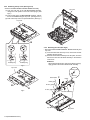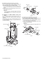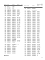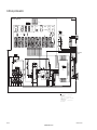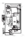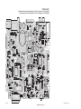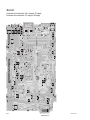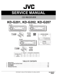
1
SERVICE MANUAL CD RECEIVER SERVICE MANUAL 2 2010 MA468<Rev.001> KD-AHD69J, KD-HDR60J COPYRIGHT © 2010 Victor Company of Japan, Limited Lead free solder used in the board (material : Sn-Ag-Cu, melting point : 219 Centigrade) Lead free solder used in the board (material : Sn-Cu, melting point : 230 Centigrade) TABLE OF CONTENTS 1 2 3 4 5 PRECAUTION. . . . . . . . . . . . . . . . . . . . . . . . . . . . . . . . . . . . . . . . . . . . . . . . . . . . . . . . . . . . . . . . . . . . . . . . . 1-3 SPECIFIC SERVICE INSTRUCTIONS . . . . . . . . . . . . . . . . . . . . . . . . . . . . . . . . . . . . . . . . . . . . . . . . . . . . . . 1-7 DISASSEMBLY . . . . . . . . . . . . . . . . . . . . . . . . . . . . . . . . . . . . . . . . . . . . . . . . . . . . . . . . . . . . . . . . . . . . . . . 1-8 ADJUSTMENT . . . . . . . . . . . . . . . . . . . . . . . . . . . . . . . . . . . . . . . . . . . . . . . . . . . . . . . . . . . . . . . . . . . . . . . 1-16 TROUBLESHOOTING . . . . . . . . . . . . . . . . . . . . . . . . . . . . . . . . . . . . . . . . . . . . . . . . . . . . . . . . . . . . . . . . . 1-22 COPYRIGHT © 2010 Victor Company of Japan, Limited No.MA468<Rev.001> 2010/2 SPECIFICATION AUDIO AMPLIFIER SECTION 20 W RMS × 4 Channels at 4 Ω and < 1% THD+N 80 dBA (reference: 1 W into 4 Ω) 4 Ω (4 Ω to 8 Ω allowance) Frequencies 45 Hz, 120 Hz, 315 Hz, 800 Hz, 2.4 kHz, 6.3 kHz, 15 kHz Level ±10 dB Frequency Response 40 Hz to 20 000 Hz Line-Out Level/Impedance KD-AHD69 5.0 V/20kΩ load (full scale) KD-HDR60 2.5 V/20 kΩ load (full scale) Subwoofer-Out Level/Im- KD-AHD69 5.0 V/20 kΩ load (full scale) pedance KD-HDR60 2.5 V/20 kΩ load (full scale) Output Impedance 1 kΩ Other Terminal USB input terminal, AUX (auxiliary) input jack, Expansion port, Steering wheel remote input (only for KD-AHD69), Antenna input TUNER SECTION (HD Radio System Compatible) Frequency Range FM with channel interval set to 100 kHz or 200 87.5 MHz to 107.9 MHz kHz with channel interval set to 50 kHz 87.5 MHz to 108.0 MHz AM with channel interval set to 10 kHz 530 kHz to 1 710 kHz with channel interval set to 9 kHz 531 kHz to 1 602 kHz FM Tuner Usable Sensitivity 8.3 dBf (0.7 µV/75 Ω) 50 dB Quieting Sensitivity 14.3 dBf (1.4 µV/75 Ω) Alternate Channel Selectiv- 65 dB ity (400 kHz) Frequency Response 20 Hz to 20 000 Hz (HD Radio broadcast) 40 Hz to 15 000 Hz (Conventional broadcast) Stereo Separation 70 dB (HD Radio broadcast) 50 dB (Conventional broadcast) Capture Ratio 3.5 dB AM Tuner Sensitivity 13 µV Selectivity 80 dB Frequency Response 40 Hz to 15 000 Hz (HD Radio broadcast) Stereo Separation 70 dB (HD Radio broadcast) CD PLAYER SECTION Type Compact disc player Signal Detection System Non-contact optical pickup (semiconductor laser) Number of Channels 2 channels (stereo) Frequency Response 5 Hz to 20 000 Hz Dynamic Range 96 dB Signal-to-Noise Ratio 98 dB Wow and Flutter Less than measurable limit MP3 Decoding Format: (MPEG1/2 Audio Layer 3) Max. Bit Rate: 320 kbps WMA (Windows Media® Audio) Decoding Format Max. Bit Rate: 192 kbps USB SECTION USB Standards USB 2.0 Full Speed Data Transfer Rate Full Speed: Maximum 12 Mbps Low Speed: Maximum 1.5 Mbps Compatible Device Mass storage class Compatible File System FAT 32/16/12 Max. Current DC 5 V 500 mA GENERAL Power Requirement Operating Voltage DC 14.4 V (11 V to 16 V allowance) Grounding System Negative ground Allowable Operating Temperature 0°C to +40°C (32°F to 104°F) Dimensions (W × H × D): Installation Size 182 mm × 52 mm × 160 mm (7-3/16” × 2-1/16” × 6-5/16”) (approx.) Panel Size 188 mm × 58 mm × 5 mm (7-7/16” × 2-5/16” × 1/4”) Mass 1.3 kg (2.9 lbs) (excluding accessories) Power Output Signal-to-Noise Ratio Load Impedance Equalizer Control Range Designs & specifications are subject to change without notice. 1-2 (No.MA468<Rev.001>) SECTION 1 PRECAUTION 1.1 Safety Precautions (1) This design of this product contains special hardware and many circuits and components specially for safety purposes. For continued protection, no changes should be made to the original design unless authorized in writing by the manufacturer. Replacement parts must be identical to those used in the original circuits. Services should be performed by qualified personnel only. voltmeter. Move the resistor connection to each exposed metal part, particularly any exposed metal part having a return path to the chassis, and measure the AC voltage across the resistor. Now, reverse the plug in the AC outlet and repeat each measurement. Voltage measured any must not exceed 0.75 V AC (r.m.s.). This corresponds to 0.5 mA AC (r.m.s.). (2) Alterations of the design or circuitry of the product should not be made. Any design alterations of the product should not be made. Any design alterations or additions will void the manufacturers warranty and will further relieve the manufacture of responsibility for personal injury or property damage resulting therefrom. (3) Many electrical and mechanical parts in the products have special safety-related characteristics. These characteristics are often not evident from visual inspection nor can the protection afforded by them necessarily be obtained by using replacement components rated for higher voltage, wattage, etc. Replacement parts which have these special safety characteristics are identified in the Parts List of Service Manual. Electrical components having such features are identified by shading on the schematics and by ( ) on the Parts List in the Service Manual. The use of a substitute replacement which does not have the same safety characteristics as the recommended replacement parts shown in the Parts List of Service Manual may create shock, fire, or other hazards. (4) The leads in the products are routed and dressed with ties, clamps, tubings, barriers and the like to be separated from live parts, high temperature parts, moving parts and/or sharp edges for the prevention of electric shock and fire hazard. When service is required, the original lead routing and dress should be observed, and it should be confirmed that they have been returned to normal, after reassembling. (5) Leakage shock hazard testing After reassembling the product, always perform an isolation check on the exposed metal parts of the product (antenna terminals, knobs, metal cabinet, screw heads, headphone jack, control shafts, etc.) to be sure the product is safe to operate without danger of electrical shock.Do not use a line isolation transformer during this check. • Plug the AC line cord directly into the AC outlet. Using a "Leakage Current Tester", measure the leakage current from each exposed metal parts of the cabinet, particularly any exposed metal part having a return path to the chassis, to a known good earth ground. Any leakage current must not exceed 0.5mA AC (r.m.s.). • Alternate check method Plug the AC line cord directly into the AC outlet. Use an AC voltmeter having, 1,000Ω per volt or more sensitivity in the following manner. Connect a 1,500Ω 10W resistor paralleled by a 0.15µF AC-type capacitor between an exposed metal part and a known good earth ground. Measure the AC voltage across the resistor with the AC AC VOLTMETER (Having 1000 ohms/volts, or more sensitivity) 0.15 F AC TYPE 1500 10W Place this probe on each exposed metal part. Good earth ground 1.2 Warning (1) This equipment has been designed and manufactured to meet international safety standards. (2) It is the legal responsibility of the repairer to ensure that these safety standards are maintained. (3) Repairs must be made in accordance with the relevant safety standards. (4) It is essential that safety critical components are replaced by approved parts. (5) If mains voltage selector is provided, check setting for local voltage. 1.3 Caution Burrs formed during molding may be left over on some parts of the chassis. Therefore, pay attention to such burrs in the case of preforming repair of this system. 1.4 Critical parts for safety In regard with component parts appearing on the silk-screen printed side (parts side) of the PWB diagrams, the parts that are printed over with black such as the resistor ( ), diode ( ) and ICP ( ) or identified by the " " mark nearby are critical for safety. When replacing them, be sure to use the parts of the same type and rating as specified by the manufacturer. (This regulation dose not Except the J and C version) (No.MA468<Rev.001>)1-3 1.5 Preventing static electricity Electrostatic discharge (ESD), which occurs when static electricity stored in the body, fabric, etc. is discharged, can destroy the laser diode in the traverse unit (optical pickup). Take care to prevent this when performing repairs. 1.5.1 Grounding to prevent damage by static electricity Static electricity in the work area can destroy the optical pickup (laser diode) in devices such as laser products. Be careful to use proper grounding in the area where repairs are being performed. (1) Ground the workbench Ground the workbench by laying conductive material (such as a conductive sheet) or an iron plate over it before placing the traverse unit (optical pickup) on it. (2) Ground yourself Use an anti-static wrist strap to release any static electricity built up in your body. (caption) Anti-static wrist strap 1M Conductive material (conductive sheet) or iron palate (3) Handling the optical pickup • In order to maintain quality during transport and before installation, both sides of the laser diode on the replacement optical pickup are shorted. After replacement, return the shorted parts to their original condition. (Refer to the text.) • Do not use a tester to check the condition of the laser diode in the optical pickup. The tester's internal power source can easily destroy the laser diode. 1.6 Handling the traverse unit (optical pickup) (1) Do not subject the traverse unit (optical pickup) to strong shocks, as it is a sensitive, complex unit. (2) Cut off the shorted part of the flexible cable using nippers, etc. after replacing the optical pickup. For specific details, refer to the replacement procedure in the text. Remove the anti-static pin when replacing the traverse unit. Be careful not to take too long a time when attaching it to the connector. (3) Handle the flexible cable carefully as it may break when subjected to strong force. (4) I t is not possible to adjust the semi-fixed resistor that adjusts the laser power. Do not turn it. 1-4 (No.MA468<Rev.001>) 1.7 Attention when traverse unit is decomposed *Please refer to "Disassembly method" in the text for the pickup unit. • Apply solder to the short land sections before the card wire is disconnected from the connector on the servo board. (If the card wire is disconnected without applying solder, the pickup may be destroyed by static electricity.) • In the assembly, be sure to remove solder from the short land sections after connecting the card wire. Mechanism control board Short land section CN102 Flexible wire Pickup (No.MA468<Rev.001>)1-5 1.8 Important for laser products 1.CLASS 1 LASER PRODUCT 2.CAUTION : (For U.S.A.) Visible and/or invisible class II laser radiation when open. Do not stare into beam. (Others) Visible and/or invisible class 1M laser radiation when open. Do not view directly with optical instruments. 3.CAUTION : Visible and/or invisible laser radiation when open and inter lock failed or defeated. Avoid direct exposure to beam. 4.CAUTION : This laser product uses visible and/or invisible laser radiation and is equipped with safety switches which prevent emission of radiation when the drawer is open and the safety interlocks have failed or are defeated. It is dangerous to defeat the safety switches. 5.CAUTION : If safety switches malfunction, the laser is able to function. 6.CAUTION : Use of controls, adjustments or performance of procedures other than those specified here in may result in hazardous radiation exposure. ! Please use enough caution not to see the beam directly or touch it in case of an adjustment or operation check. REPRODUCTION AND POSITION OF LABELS and PRINT WARNING LABEL and PRINT 1-6 (No.MA468<Rev.001>) SECTION 2 SPECIFIC SERVICE INSTRUCTIONS This service manual does not describe SPECIFIC SERVICE INSTRUCTIONS. (No.MA468<Rev.001>)1-7 SECTION 3 DISASSEMBLY 3.1 Main body 3.1.1 Removing the Bottom chassis (See Fig.1) (1) Remove the two screws A and one screw B attaching the Heat sink. (2) Remove the one screws C and one screw D attaching the Bottom chassis. (3) Remove the three screws H attaching the Main board. (See Fig.5) (4) Disconnect the B-B connector connected CD mechanism and Main board CN481 of the Main board. (See Fig.5) CN481 H C D A B H A Fig.1 3.1.2 Removing the Front chassis (See Fig.2) (1) Disengage hour hooks a engaged Front chassis. Fig.5 3.1.4 Removing the CD mechanism (See Fig.6) (1) Remove the three screws J attaching the CD mechanism. hook a J Fig.2 3.1.3 Removing the Main board (see Fig.3, 4, 5) (1) Remove the one screw E attaching the Top chassis. (See Fig.3) E Fig.3 (2) Remove the two screws F and one screw G attaching the Side plate. (See Fig.4) J Fig.6 3.1.5 (1) (2) (3) Removing the Switch board (See Fig.7) Remove the Volume knob. Remove the four screws K attaching the Rear cover. Disengage eleven hooks b engaged Rear cover. hook b F G F Fig.4 K hook b Fig.7 1-8 (No.MA468<Rev.001>) K 3.2 CD MECHANISM assembly section • Remove the CD MECHANISM assembly from the main body. 3.2.1 Removing the MECHANISM CONTROL BOARD assembly (See Fig.1 and 2) (1) From the bottom side of CD MECHANISM assembly, remove the solders from the soldered sections (a, b and c) on the MECHANISM CONTROL BOARD assembly. (See Fig.1.) (2) Remove the three screws A attaching the MECHANISM CONTROL BOARD assembly. (See Fig.1.) (3) Solder the short land sections on the pickup. (See Fig.2.) b a Caution: • Solder the short land sections on the pickup before disconnecting the flexible wire from the connector CN102 on the MECHANISM CONTROL BOARD assembly. If the card wire is disconnected without attaching solder, the pickup may be destroyed by static electricity. (See Fig.2.) • When attaching the MECHANISM CONTROL BOARD assembly, remove the solders from the short land sections after connecting the flexible wire to the connector CN102 on the MECHANISM CONTROL BOARD assembly. Mechanism control board CN102 A c A A Fig.1 Mechanism control board Short land section CN102 Flexible wire Pickup Fig.2 (No.MA468<Rev.001>)1-9 3.2.2 Removing the top cover (See Fig.3 to 5) • Remove the MECHANISM CONTROL BOARD assembly. (1) From the front side of the CD MECHANISM assembly, change the hook position of the two roller springs. (See Fig.3.) (2) From the side of the CD MECHANISM assembly, remove the six screws B attaching the top cover. (See Fig.3 and 4.) (3) Take out the top cover in an upward direction. (See Fig.5.) Top cover Top cover B Fig.5 3.2.3 Removing the roller (See Fig.6) • Remove the MECHANISM CONTROL BOARD assembly and top cover. (1) From the bottom side of the top cover, remove the screw C attaching the gear holder. (2) Remove the R.holder assembly from disc plate, and then take out the roller from R.holder assembly in the direction of the arrow. Roller spring Reference: When attaching the R.ACT gear (2) and R.ACT gear (3), apply grease to the section d of R.holder assembly. Roller spring Fig.3 Top cover Roller coller Washer Gear holder C Roller Roller gear R.ACT gear(3) B B Fig.4 R.ACT gear(2) d R.holder assembly Top cover Disc plate Fig.6 1-10 (No.MA468<Rev.001>) 3.2.4 Removing the PHOTO BOARD assembly (See Fig.7 and 8) • Remove the MECHANISM CONTROL BOARD assembly and top cover. (1) From the bottom side of the top cover, release the projection e from the notch of the disc plate. (See Fig.7.) (2) Take out the disc plate in the direction of the arrow. (See Fig.7.) (3) From the reverse side of the disc plate, remove the screw D attaching the PHOTO BOARD assembly. (See Fig.8.) Mechanism section SUS spring Mecha frame SUS spring e e E Top cover Disc plate Fig.7 SUS spring D Roller spring Loading motor assembly Fig.9 F SUS spring Cam cover Photo board Disc plate Fig.8 3.2.5 Removing the mechanism section (See Fig.9 and 10) • Remove the MECHANISM CONTROL BOARD assembly and top cover. (1) From the top side of the CD MECHANISM assembly, remove the two screws E attaching the loading motor assembly. (See Fig.9.) (2) Remove the two roller springs on the top side of the mecha frame. (See Fig.9.) (3) Remove the four SUS springs on the top side of the mecha frame. (See Fig.9.) (4) Remove the link spring on the top side of the mecha frame. (See Fig.10.) (5) Release section f of the three dampers from the mecha frame. (See Fig.10.) Mecha frame Fig.10 Reference: When attaching the roller spring and SUS spring, keep direction before remove. (6) Move the slide cam (R) assembly in the direction of the arrow, and then take out the mechanism section in an upward direction. (See Fig.10.) Reference: When attaching the mechanism section, apply grease to the section g. (See Fig.10.) (No.MA468<Rev.001>)1-11 3.2.6 Removing the slide cam (L) (See Fig.11 to 13) • Remove the MECHANISM CONTROL BOARD assembly, top cover and mechanism section. (1) From the top side of the mecha frame, remove the screw F attaching the cam cover. (See Fig.11.) (2) Take out the cam cover from mecha frame in an upward direction. (See Fig.11.) (3) Take out the slide cam (L) in the direction of the arrow. (See Fig.12.) Slide cam(L) Reference: When attaching the slide cam (L), apply grease to the section h. (See Fig.13.) F Cam cover Mecha frame Fig.12 h Slide cam(L) h h h Mecha frame h Slide cam(L) h Fig.11 h h Fig.13 1-12 (No.MA468<Rev.001>) 3.2.7 Removing the F.lock lever and slide cam (R) (See Fig.14 and 15) • Remove the MECHANISM CONTROL BOARD assembly, top cover and mechanism section. (1) From the top side of the mecha frame, take out the slide cam (R) assembly in an upward direction. (See Fig.14.) (2) Rotate the F.lock lever in the direction of the arrow 1, and then take out the direction of the arrow 2. (See Fig.14.) 3.2.8 Removing the damper (See Fig.16) • Remove the MECHANISM CONTROL BOARD assembly, top cover and mechanism section. From the mechanism section, pull out the three dampers in the direction of the arrow. Reference: Before inserting the shaft to the dampers, apply IPA to the pocket j of damper. Reference: When attaching the slide cam (R) assembly, the f.lock lever and the link arm apply grease to the section h. (See Fig.14 and 15.) Slide cam(R) assembly Damper (Gray) Damper (Brown) j h 2 F.lock lever 1 j h h Damper (Brown) j Fig.16 Mecha frame h h Link arm Fig.14 Slide cam(R) assembly h h 3.2.9 Removing the clamper assembly (See Fig.17) • Remove the MECHANISM CONTROL BOARD assembly, top cover and mechanism section. (1) From the top side of the mechanism section, release the clamper spring. (2) Move the clamper assembly in the direction of the arrow, and then release the joints (k and m). (3) Take out the clamper assembly from the T.M chassis assembly. h h h h Clamper assembly h Clamper spring Slide cam(R) assembly k Fig.15 T.M. chassis assembly m Fig.17 (No.MA468<Rev.001>)1-13 3.2.10 Removing the feed motor (See Fig.18 and 19) • Remove the MECHANISM CONTROL BOARD assembly, top cover, mechanism section and clamper assembly. (1) From the bottom side of the T.M chassis assembly, remove the two screws G attaching the feed motor assembly. (See Fig.18.) (2) Remove the two screws H attaching the feed motor to f.motor holder. (See Fig.19.) Feed motor Reference: When attaching the f. wheel gear, trigger arm and feed motor, apply grease to the sections (n, p and q). (See Fig.18 and 19.) 3.2.11 Removing the SWITCH BOARD assembly (See Fig.18) • Remove the MECHANISM CONTROL BOARD assembly, top cover, mechanism section, clamper assembly and feed motor assembly. From the bottom side of the T.M chassis assembly, take out the SWITCH BOARD assembly in an upward direction from T.M chassis assembly. G p Feed motor assembly Comp. spring F.worm gear q H F.motor holder Fig.19 3.2.12 Removing the loading motor (See Fig.20) • Remove the MECHANISM CONTROL BOARD assembly, top cover, mechanism section and clamper assembly. (1) From the right side of the L.M base assembly, remove the two screws J attaching the loading motor. (2) Take out the loading motor in the direction of the arrow from the L.M base assembly. Reference: When attaching the loading motor, apply grease to the section r. Trigger arm J L.worm gear Switch board n Loading motor r F.wheel gear L.M. base assembly Fig.20 T.M. chassis assembly Fig.18 1-14 (No.MA468<Rev.001>) 3.2.13 Removing the pickup assembly (See Fig.21 to 22) • Remove the MECHANISM CONTROL BOARD assembly, top cover, mechanism section, clamper assembly and feed motor assembly. Caution: • Do not touch section u on the pickup assembly. (See Fig.21 and 22.) (1) From the bottom side of the T.M chassis assembly, move the pickup assembly in the direction of the arrow from the T.M chassis assembly. (See Fig.21.) (2) Pull out the main shaft. (See Fig.21.) (3) Remove the screw K attaching the pickup to the rack plate. (See Fig.22.) Reference: When attaching the loading motor, apply grease to the sections s and t. (See Fig.21.) t Main shaft Pick up assembly 3.2.14 Removing the spindle motor (See Fig.23 and 24) • Remove the MECHANISM CONTROL BOARD assembly, top cover, mechanism section, clamper assembly, feed motor assembly and pickup assembly. (1) From the top side of the T.M chassis assembly, remove the CD T.table assembly from the spindle motor. (See Fig.23.) (2) Remove the two screws L attaching the spindle motor. (See Fig.23.) (3) Take out the spindle motor from the bottom side of the T.M chassis assembly. (See Fig.23.) Reference: When attaching the CD T.table assembly to the spindle motor shaft, apply loctite 460 to inside the CD T.table assembly. (See Fig.24.) L L CD T.table assembly u T.M.chassis assembly Spindle motor Fig.23 s CD T.table assembly Loctite T.M. chassis assembly Fig.21 K Rack plate u Spindle motor Fig.24 Pick up Fig.22 (No.MA468<Rev.001>)1-15 SECTION 4 ADJUSTMENT 4.1 (1) (2) (3) (4) 4.2 Test instruments required for adjustment Digital oscilloscope (100MHz) Digital tester Test Disc JVC :CTS-1000 Extension cable for check EXTSH002-22P x 1 Standard volume position Balance and Bass &Treble volume : lndication"0" Loudness : OFF 4.4 Standard measuring conditions Power supply voltage DC14.4V(10.5 to 16V) Load impedance 20K.(2 Speakers connection) Output Level Line out 2.5V (Vol. MAX) 4.5 4.3 Dummy load Exclusive dummy load should be used for AM,and FM. For FM dummy load, there is a loss of 6dB between SSG outputand antenna input. The loss of 6dB need not be considered sincedirect reading offigures are applied in this working standard. How to connect the extension cable for adjusting Caution: Be sure to attach the heat sink and rear bracket onto the power amplifier IC and regulator IC respectively, before supply the power. If voltage is applied without attaching these parts, the power amplifier IC and regulator IC will be destroyed by heat. Extension cable EXTSH002-22P 1-16 (No.MA468<Rev.001>) 4.6 SERVICE MODE 4.6.1 Service mode setting (1) Push POWER BUTTON (Power ON) (2) Set to service mode Keep this state more 3 seconds while continuing pressing the [MENU] button and [DISC DOWN] button scquentially. *Exchanging of operate a menu of a service mode with the [FF] button and [REW] button. Operate choice of a menu with a [ENT] button. SERVICE MODE DATA DELETE INIT ALL Initialize EEPROM data CDERR DEL Clear CD error history CHERR DEL Clear changer error history : The error history saved in the CD changer is cleared. DSPERR DEL Clear DSP error history Note : A disc is inseted, and it is displayed only at the timer of CD function. RUNNING CDLD ON TUBUYAKI ERROR READ ROM CORRE MODE 1 For use in running tests MODE 2 For use in running tests xx yy zz CD laser illumination and electric current (mA) xx : Early current value yy : Current current value zz : Difference value Only the factory setup. No use. CD ERROR Read CD error history CH ERROR Read CD changer error history : The error history saved on the CD changer is read out. DSP ERROR Read DSP error history ROMVERxx ROM correction version (No.MA468<Rev.001>)1-17 TUNER ADJ AUTO ADJ Only factory setup. No use. MANUAL ADJ ADJ1 1. FM DAA 87.5 40dBuV 0% Press OK ADJ2 2. FM DAA 97.9 40dBuV 0% Press OK ADJ3 3. FM DAA 108.0 40dBuV 0% Press OK ADJ4 4. FM S Meter 97.9 30dBuV 0% Press OK ADJ5 5. FM S Meter 97.9 60dBuV 0% Press OK ADJ6 6. FM Full Sepa 97.9 70dBuV 0% Lch Press OK ADJ7 7. FM IF Counter 97.9 70dBuV 0% Press OK ADJ8 8. AM S Meter 999 26dBuV 0% Press OK ADJ9 9. AM S Meter 999 56dBuV 0% Press OK ADJ10 10. AM IF Counter 999 56dBuV 0% Press OK Manual Adjust COMPLETED 1. FM DAA 87.5 40dBuV 0% No signal 2. FM DAA 97.9 40dBuV 0% No signal 3. FM DAA 108.0 40dBuV 0% No signal 4. FM S Meter 97.9 30dBuV 0% High or Low or No signal 5. FM S Meter 97.9 60dBuV 0% High or Low or No signal 6. FM Full Sepa 97.9 60dBuV 0% Adjust NG or No signal 7. FM IF Counter 97.9 60dBuV 0% Adjust NG or No signal 8. FM IF Counter 999 26dBuV 0% High or Low or No signal 9. AM S Meter 999 56dBuV 0% High or Low or No signal 10. AM IF Counter 999 56dBuV 0% Adjust NG or No signal POWER POWER OFF (Adjust Mode FINISH) 1-18 (No.MA468<Rev.001>) 4.7 (1) (2) (3) (4) Confirmation method of a micon version Push POWER BUTTON (Power ON). Set this set at tuner mode. Keep this state more than 3 seconds while continuing pressing the [ENT] button and [MENU] button sequentially. It is displayed as follows by a display window. MAIN V䌸䌸䌸 Main micon version CD V䌸䌸䌸-䌸䌸 CD module version and ROM corre version CH V䌸䌸䌸 CH micon version (It is displayed only in changer connection.) BTC-䌸䌸 Software version of BT core (It is displayed in bluetooth adaptor connection.) BHH-䌸䌸䌸 Hardtware version of BT Module (It is displayed in bluetooth adaptor connection.) BHS-䌸䌸䌸 Software version of BT Module (It is displayed in bluetooth adaptor connection.) BHC-䌸䌸䌸 Software version of BT Hideaway controller (It is displayed in bluetooth adaptor connection.) ADR-䌸䌸䌸䌸䌸䌸 BT Address (It is displayed in bluetooth adaptor connection.) HD-xxxx-xxx HD decoder firmware version Change each indication with the [FF] button and [REW] button. 4.8 Error code tables 4.8.1 Mechanism error code Error contents Details Error code Detailed error code Disc loading error (1) B1 time out (2) C1 time out (3) B2 time out 09 09 09 0011 0012 0015 Eject error (1) B1 time out (2) C2 time out (3) B2 time out 01 01 01 0023 0026 0027 Compulsion eject error (1) E1 compulsion eject error (2) E2 compulsion eject error (3) E3 compulsion eject error (4) E5 compulsion eject error (5) E7 compulsion eject error (6) E8 compulsion eject error (7) E9 compulsion eject error 01 01 01 01 01 01 01 0041 0042 0043 0045 0047 0048 0049 4.8.2 Disc error code Error contents Details Error code Detailed error code TOC read error TOC lead movement of a CD is not completed. 84 0059 First track access error Even if TOC reading passes after the end with CD running mode for 30 seconds, the first track access is not finished. 80 0060 Last track access error Even if TOC reading passes after the end with CD running mode for 30 seconds, the first track access is not finished. 80 0061 NO DISC judgment Judgment without disc. 80 0090 It is NO DISC by start failure Start is impossible. 80 0091 It is stopped by playback inability Stop in running mode playback 80 0093 Logic format NG 80 0094 Logic format analysis inability or non-correspondence logic format. (No.MA468<Rev.001>)1-19 4.8.3 CD changer mechanism error code Error contents Tray eject error (1) TRAYINSW time over (TRAYINSW:L,TRAYOUTSW:H) (2) TRAYOUTSW time over (TRAYINSW:H,TRAYOUTSW:H) (3) TRAYINSW time over (TRAYINSW:L,TRAYOUTSW:L) (4) MAGIN SW:L→H Tray return error (1) TRAYOUTSW time over (TRAYINSW:H,TRAYOUTSW:L) (2) TRAYINSW time over (TRAYINSW:H,TRAYOUTSW:H) (3) TRAYIN/OUTSW time over (TRAYINSW:L,TRAYOUTSW:L) (4) MAGIN SW:L→H Details Error code Detailed error code Tray motor time over Tray motor does not operate. 03 0011 Tray stops. 03 0012 TRAYINSW NG etc. 03 0013 Magazine is ejected while Tray is being ejected. 03 0014 Tray motor time over Tray motor does not operate. 03 0016 Tray stops. 03 0017 TRAYINSW NG etc. 03 0018 Magazine is ejected while Tray is being ejected. 03 0019 Lifter up error (1) WAIT position time over (2) WAIT position time over (3) WAIT position time over Position motor time over Position motor does not operate. Position is not stable in fine adjustment mode. Other condition 02 02 02 0021 0022 0023 Lifter down error (1) WAIT position time over (2) WAIT position time over (3) WAIT position time over Position motor time over Position motor does not operate. Position is not stable in fine adjustment mode. Other condition 02 02 02 0026 0027 0028 Chucking error (1) Play position time over (2) Play position time over (3) Play position time over Position motor time over Position motor does not operate. Position is not stable in fine adjustment mode. Other condition 02 02 02 0031 0032 0033 Unchucking error (1) WAIT position time over (2) WAIT position time over (3) WAIT position time over Position motor time over Position motor does not operate. Position is not stable in fine adjustment mode. Other condition 02 02 02 0036 0037 0038 Eject error (1) Eject position time over (2) Eject position time over (3) MAGINSW time over Eject cannot be carried out. Position motor does not operate. Improper EJECT position.* Magazine is not ejected. 02 02 01 0041 0042 0043 Initialize error (1) Eject position time over (2) Eject position time over TRAYINSW and TRAYOUTSW are L. Position is not stable in absolute position.* 03 02 0046 0047 *"Position is not stable in WAIT position," "Position is not stable in PLAY position," and "Position is not stable in absolute position," and "Improper EJECT position" are all Position Motor TIME OVER. 1-20 (No.MA468<Rev.001>) 4.8.4 CD changer disc error code Error contents Pickup movement error (1) Time over of pickup movement in an inner direction(10s) (2) Time over of pickup movement in an outer direction(10s) Details Time over at PUBWD and PUFWD by monitoring RESET SW. Pickup cannot move in an inner direction. RESET SW is not on. Pickup cannot move in an inner direction. RESET SW is not off. Error code Detailed error code 04 0051 04 0052 Focus search error When focus is not adjusted by 3-round(1set) focus search after Focus is not adjusted by 3-round disc change or focus shock, the result is NG focus search 81 0053 Tracking balance adjustment error Tracking balance adjustment is not finished 1s after adjustment Time over(1s) command(TBA) is executed. 82 0054 TOC area search error Time over(10s) TOC area search is not finished after 10s. 80 0055 Focus balance adjustment error Time over(2s) Focus balance adjustment is not finished 2s after adjustment command(FBA) is executed. 82 0056 Focus gain adjustment error Time over(0.6s) Focus gain adjustment error is not finished 0.6s after adjustment command(FGA) is executed. 82 0057 Tracking gain adjustment error Time over(0.6s) Tracking gain adjustment error is not finished 0.6s after adjustment command(TGA) is executed. 82 0058 TOC read error. Time over(30s) TOC read operation is not finished after 30s. 84 0059 First track access error Time over(10s) First track access is not finished 10s after TOC reading is finished. 80 0060 Last track access error Time over(10s) Last track access is not finished 10s after first track in running mode. 80 0061 Q code read error Time over(0.6s) Q code is not read for 0.6s during playback of TOC and program area. 80 0062 (No.MA468<Rev.001>)1-21 SECTION 5 TROUBLESHOOTING 16 PIN CORD DIAGRAM GN 8 WH 9 7 GN/BK WH/BK 10 VI/BK 5 VI GY 12 4 NC NC 13 NC 14 3 BL/WH 2 RD 1 BK 1 BK 16 YL 15 OR/WH 2 RD 8 GN 7 GN/BK 5 VI 6 VI/BK 9 WH 10 WH/BK 12 GY 11 GY/BK 3 BL/WH 1-22 (No.MA468<Rev.001>) GY/BK 11 6 OR/WH 15 YL 16 BK Black GN Green RD Red GY Gray BL Blue OR Orange WH White YL Yellow VI Violet Victor Company of Japan, Limited Mobile Entertainment Division 10-1,1chome,Ohwatari-machi,Maebashi-city,371-8543,Japan (No.MA468<Rev.001>) Printed in Japan VSE PARTS LIST KD-AHD69J, KD-HDR60J MODEL MARK KD-AHD69J A KD-HDR60J B * All printed circuit boards and its assemblies are not available as service parts. - Contents Exploded view of general assembly and parts list (Block No.M1) CD mechanism assembly and parts list (Block No.MB) Packing materials and accessories parts list (Block No.M3) MA468PAR<Rev.001> 3- 2 3- 5 3-14 3-1 Exploded view of general assembly and parts list Block No. M 1 M M 23 13 12 12 5 10 56 b a 1 a 7 18 A 17 6 43 20 19 42 39 6 16 38 43 27 6 36 31 28 Switch board 37 29 32 30 24 35 34 40 41 26 44 33 47 25 48 46 3-2 Block No. M 1 M M 52 51 15 55 b 56 a Main board 53 HD board 7 18 7 54 17 21 7 20 9 A 16 8 43 9 4 8 2 49 3 14 45 44 11 50 47 48 46 22 The parts without symbol number are not service. 3-3 General Assembly Block No. [M][1][M][M] 3-4 Symbol No. Part No. Part Name 1 2 3 3 4 5 6 7 8 9 10 11 12 13 14 15 16 17 18 19 20 21 22 22 23 24 24 25 25 26 27 28 29 30 31 32 32 33 33 34 35 35 36 37 38 39 40 40 41 42 43 44 45 46 47 48 49 50 51 52 53 54 55 56 GE10253-007A GE33234-002A GE20232-008A GE20232-009A GE32830-004A GE40395-002A QYSDST2604ZA GE40377-002A GE40377-003A GE40377-003A GE40377-002A QYSDSF2606ZA GE40377-001A GE40377-001A GE40377-002A LV40847-048A GE10242-016A GE33792-001A GE40368-002A GE32810-001A GE30999-004A GE40432-001A LV38918-001A LV38917-001A GE40442-001A GE33886-002A GE33886-003A GE33885-024A GE33885-025A GE40463-001A GE33800-002A GE33801-002A GE33802-004A GE33803-001A GE40495-001A GE33805-003A GE33805-001A GE33806-018A GE33806-017A GE33807-001A GE33808-003A GE33808-001A GE33809-002A GE33810-001A GE33881-002A GE30999-009A GE33704-006A GE33704-001A GE40127-006A GE10273-003A VKZ4777-010 GE33813-001A GE33814-001A GE33815-001A GE40482-001A QLD0631-001 QNZ1002-001 QNZ1003-001 LV40848-086A QMFZ064-150-J1 LV38578-001A LV38660-001A GE40354-001A GE40308-001A TOP CHASSIS HEAT SINK BOTTOM COVER BOTTOM COVER INSULATOR SIDE PANEL TAP SCREW SCREW SPECIAL SCREW SPECIAL SCREW SCREW TAP SCREW SCREW SCREW SCREW SPACER(H) FRONT CHASSIS LOCK LEVER TORSION SPRING RELEASE LEVER COMP.SPRING BLIND NAME PLATE NAME PLATE FCC RULE LABEL FRT PANEL ASSY FRT PANEL ASSY FINDER ASSY FINDER ASSY JVC BADGE EJECT BUTTON SOURCE BUTTON NAVI BUTTON DISP BUTTON MENU BTN ASSY BUTTON RIM BUTTON RIM PHONE BACK BTN PHONE BACK BTN RIM LENS RIM COVER RIM COVER LIGHT GUIDE RUBBER BASE DETACH BUTTON COMP.SPRING VOLUME KNOB VOLUME KNOB KNOB SPRING REAR COVER MINI SCREW LCD LENS LENS CASE LCD CASE LIGHTING SHEET LCD MODULE RUBBER CONNE RUBBER CONNE SPACER(P) FUSE SHIELD CASE PWB SHIELD IC BRACKET REG IC BRACKET Description Local A B M2.6 x 4mm(x3) (x3) (x2) M2.6 x 6mm (x2) A B A B A B A B A B A B A B (x4) 15A CD mechanism assembly and parts list Block No. M B M M FMU-CD3-11D Grease 41 48 47 JVG-31N FG-87HS 42 JVS-1003 A 43 23 50 F 46 45 Photo board 70 43 43 60 31 D 57 D 44 C 58 66 30 28 49 74 B 45 59 Rest switch board E 62 B 29 43 32 27 7 Back side F 38 5 10 56 G 61 34 3 54 35 2 55 51 34 9 53 6 52 39 4 36 8 48 G 36 37 11.1mm 0.1mm A 48 48 C 14 33 21 1 14 16 61 72 20 48 E Mecha control board 19 13 11.1mm 0.1mm 63 63 11 12 17 18 15 71 63 The parts without symbol number are not service. 3-5 CD mechanism Block No. [M][B][M][M] 3-6 Symbol No. Part No. Part Name 1 2 3 4 5 6 7 8 9 10 11 12 13 14 15 16 17 18 19 20 21 23 27 28 29 30 31 32 33 34 35 36 37 38 39 41 42 43 44 45 46 47 48 49 50 51 52 53 54 55 56 57 58 59 60 61 62 63 70 71 72 73 74 LV11256-001A LV36800-002A LV44658-001A LV22300-002A LV22298-002A LV36802-001A LV44552-001A LV36803-002A LV36804-002A VKZ4539-054 QAR0373-002 QYSPSPT2025MA LV36903-003A VKZ4539-054 LV36806-001A LV36805-002A LV36807-001A LV36808-001A LV36809-001A LV36810-001A QYWDL1230250 CM-FLMCD1D QAL0993-001 LV44555-001A LV36799-001A LV45227-001A QYSPSGT1745ZA LV36813-001A QAR0144-003 QYSPSPT2025MA LV22296-001A VKZ4539-054 LV36814-001A LV36815-002A LV36816-001A LV37326-003A LV44557-002A LV44558-001A LV36820-001A LV36904-001A LV37061-001A LV11260-003A VKZ4539-054 LV11264-003A LV44586-001A LV36801-002A VKZ4539-054 LV36821-001A LV36822-001A LV36823-001A LV44559-003A LV22744-001A LV44560-001A LV44590-001A LV45268-001A LV44562-002A QAL0817-003 VKZ4539-054 WJS0085-001A-E LV34916-002A LV38008-001A LV45269-001A LV45270-001A MECHA FRAME LINK ARM LINK SPRING SLIDE CAM (L) SLIDE CAM(R) LOAD RACK RETURN SPRING F LOCK LEVER CAM COVER MINI SCREW MOTOR SCREW L M BASE ASSY MINI SCREW L WORM GEAR M WHEEL GEAR A WHEEL GEAR R ACT GEAR(1) LOAD ACT GEAR LOADING GEAR SLIT WASHER SPINDLE MOTOR ASSY PICK UP MAIN SHAFT RACK PLATE RACK SPRING TAP SCREW SUB GUIDE CAP MOTOR SCREW F MOTOR HOLDER MINI SCREW F WORM GEAR F WHEEL GEAR TRIGGER ARM CLAMPER ASSY CLAMPER SPRING SUS SPRING WIRE HOLDER DAMPER DAMPER TOP COVER MINI SCREW DISC PLATE SPECIAL SCREW GEAR HOLDER MINI SCREW R ACT GEAR(2) R ACT GEAR(3) ROLLER GEAR ROLLER SHAFT R HOLDER ASSY 2 ROLLER WASHER ROLLER COLLAR 2 ROLLER SPRING FPC MINI SCREW E-FL/RB WIRE WIRE CLAMP PWB INSULATOR R HOLDER ROD WASHER 2 Description M2 x 2.5mm(x2) (x2) 3mm/1.2mm x 0.25mm M1.7 x 4.5mm 2.0V DC M2 x 2.5mm(x2) (x2) (x4) (x2) (x4) (x2) (x2) (x3) Local Electrical parts list Main board Symbol No. Block No. [0][1] Symbol No. Part No. Part Name IC10 IC221 IC221 IC261 IC272 IC301 IC401 IC402 IC411 IC412 IC413 IC501 IC501 IC512 IC541 IC701 IC702 IC703 IC703 IC710 IC801 IC871 IC872 IC872 IC901 IC931 IC951 SAF7746HW/N100 NJM4580E-X NJM4565E-X NJM2792V-X BD3461FS-X TB2926CHQ MM1701CH-X NJM2855DL1-33-X NJM2855DL1-18-X NJM2855DL1-33-X NJM2878F4-15-X TEF7000HN/V2 or TEF7000HN/V2S BA50BC0FP-X TC94A92FG-301 JVM458A S-80824CNNB-G-W R1EX24256ASAS-X or M24256-BWMN6-X TC74VHCT126AFTX TMP92CD28AF7C78 MFI341S2162-X R1EX24004ASAA-X or M24C04-RMN6-X R2S25400DS-E NJM2878F3-33-X BD9300FV-X IC IC IC IC IC IC IC IC IC IC IC IC IC IC IC IC(MCU) IC IC IC IC IC(MCU) IC IC IC IC IC IC Q311 Q391 Q393 Q394 Q410 Q411 Q703 Q881 Q882 Q901 Q902 Q903 Q951 Q952 Q953 Q954 Q955 Q956 Q5411 Q6411 Q9001 RT1N141C-X RT1P141C-X RT1P141C-X 2SC1623A/5-6/-X 2SB1424/QR/-W RT1N144C-X RT1N441C-X ISA1530AC1/QR/X RT1N144C-X RT2N03M-X RT2P03M-X 2SA812A/5-6/-X RSQ035P03-W RSQ035P03-W 2SC1623A/5-6/-X RT1P141C-X 2SC1623A/5-6/-X 2SA812A/5-6/-X IMX9-W 2SD1781K/QR/-X 2SC1623A/5-6/-X DIGI TRANSISTOR DIGI TRANSISTOR DIGI TRANSISTOR TRANSISTOR TRANSISTOR DIGI TRANSISTOR TRANSISTOR TRANSISTOR DIGI TRANSISTOR DIGI TRANSISTOR DIGI TRANSISTOR TRANSISTOR MOS FET MOS FET TRANSISTOR DIGI TRANSISTOR TRANSISTOR TRANSISTOR PAIR TRANSISTOR TRANSISTOR TRANSISTOR D391 D393 D394 D503 D504 D702 D703 D771 D772 D901 D904 D905 D951 D969 D2411 D7401 D7404 D7405 D7406 D7407 D7408 D7410 HSU119-X RKZ3.3B2KG-X RKZ10B2KG-X 1SS390-X 1SS390-X HSU119-X RKZ4.7B2KG-X HSU119-X RKZ6.2B2KG-X 1N5401-BPC04 CRS03-W CRS03-W RB051L-40-X HSU119-X MC2836-X RKZ6.2B2KG-X RKZ6.2B2KG-X RKZ6.2B2KG-X RKZ6.2B2KG-X RKZ6.2B2KG-X RKZ6.2B2KG-X RKZ6.2B2KG-X SI DIODE Z DIODE Z DIODE SI DIODE SI DIODE SI DIODE Z DIODE SI DIODE Z DIODE SI DIODE SB DIODE SB DIODE SB DIODE SI DIODE DIODE Z DIODE Z DIODE Z DIODE Z DIODE Z DIODE Z DIODE Z DIODE Description Local A B A A Part No. Part Name D7411 D7412 D7413 D7414 D7415 D7416 D7417 RKZ6.2B2KG-X RKZ6.2B2KG-X RKZ6.2B2KG-X RKZ6.2B2KG-X RKZ6.2B2KG-X RKZ6.2B2KG-X RKZ6.2B2KG-X Z DIODE Z DIODE Z DIODE Z DIODE Z DIODE Z DIODE Z DIODE C18 C21 C22 C24 C31 C34 C35 C36 C37 C38 C39 C41 C42 C43 C44 C45 C46 C48 C50 C51 C52 C53 C54 C55 C56 C57 C58 C60 C62 C63 C64 C68 C69 C72 C73 C87 C91 C92 C94 C95 C96 C97 C119 C120 C315 C316 C317 C327 C328 C392 C395 C401 C403 C404 C405 C407 C408 C411 C412 C413 C414 C416 C417 C420 C421 C422 C481 C482 QEKJ0JM-107Z NDC31HJ-471X QEKJ0JM-227Z NDC31HJ-391X QEKJ0JM-107Z NCB31HK-331X NCB31CK-105X NCB31CK-105X NCB31CK-105X NCB31CK-104X NCB31CK-104X NCB31EK-223X NDC31HJ-8R0X NDC31HJ-100X NCB31HK-102X NCB31HK-102X NCB31CK-105X NCB31HK-103X NCB31CK-105X QEKJ0JM-476Z NCB31CK-105X NCB31CK-105X NCB31CK-105X NCB31CK-104X NDC31HJ-101X NDC31HJ-101X NCB31CK-105X NCB31CK-104X NCB31EK-223X QEKJ0JM-337Z NCB31CK-104X NCB31CK-104X NCB31EK-223X NCB31EK-223X NCB31CK-104X QEKJ0JM-107Z QEKJ0JM-107Z NCB31CK-104X NCB31CK-104X NCB31CK-104X NCB31HK-332X NCB31CK-104X NDC31HJ-220X NDC31HJ-220X QEKJ1HM-225Z QEKJ1HM-475Z QEKJ1CM-476Z QEKJ1HM-225Z QEKJ1EM-106Z QERF1CM-476Z QEKJ1CM-107Z QEKJ0JM-107Z QEKJ0JM-107Z NCB31CK-104X NCB31HK-103X NCB31CK-104X NCB31CK-104X QERF1CM-476Z NCB31CK-104X NCB31HK-103X QEKJ0JM-107Z NCB31CK-104X NCB31CK-104X NCB31CK-104X NCB31CK-104X QEKJ0JM-476Z NCB31HK-103X NCB31HK-103X E CAPACITOR C CAPACITOR E CAPACITOR C CAPACITOR E CAPACITOR C CAPACITOR C CAPACITOR C CAPACITOR C CAPACITOR C CAPACITOR C CAPACITOR C CAPACITOR C CAPACITOR C CAPACITOR C CAPACITOR C CAPACITOR C CAPACITOR C CAPACITOR C CAPACITOR E CAPACITOR C CAPACITOR C CAPACITOR C CAPACITOR C CAPACITOR C CAPACITOR C CAPACITOR C CAPACITOR C CAPACITOR C CAPACITOR E CAPACITOR C CAPACITOR C CAPACITOR C CAPACITOR C CAPACITOR C CAPACITOR E CAPACITOR E CAPACITOR C CAPACITOR C CAPACITOR C CAPACITOR C CAPACITOR C CAPACITOR C CAPACITOR C CAPACITOR E CAPACITOR E CAPACITOR E CAPACITOR E CAPACITOR E CAPACITOR E CAPACITOR E CAPACITOR E CAPACITOR E CAPACITOR C CAPACITOR C CAPACITOR C CAPACITOR C CAPACITOR E CAPACITOR C CAPACITOR C CAPACITOR E CAPACITOR C CAPACITOR C CAPACITOR C CAPACITOR C CAPACITOR E CAPACITOR C CAPACITOR C CAPACITOR Description Local 100uF 6.3V M 470pF 50V J 220uF 6.3V M 390pF 50V J 100uF 6.3V M 330pF 50V K 1uF 16V K 1uF 16V K 1uF 16V K 0.1uF 16V K 0.1uF 16V K 0.022uF 25V K 8pF 50V J 10pF 50V J 1000pF 50V K 1000pF 50V K 1uF 16V K 0.01uF 50V K 1uF 16V K 47uF 6.3V M 1uF 16V K 1uF 16V K 1uF 16V K 0.1uF 16V K 100pF 50V J 100pF 50V J 1uF 16V K 0.1uF 16V K 0.022uF 25V K 330uF 6.3V M 0.1uF 16V K 0.1uF 16V K 0.022uF 25V K 0.022uF 25V K 0.1uF 16V K 100uF 6.3V M 100uF 6.3V M 0.1uF 16V K 0.1uF 16V K 0.1uF 16V K 3300pF 50V K 0.1uF 16V K 22pF 50V J 22pF 50V J 2.2uF 50V M 4.7uF 50V M 47uF 16V M 2.2uF 50V M 10uF 25V M 47uF 16V M 100uF 16V M 100uF 6.3V M 100uF 6.3V M 0.1uF 16V K 0.01uF 50V K 0.1uF 16V K 0.1uF 16V K 47uF 16V M 0.1uF 16V K 0.01uF 50V K 100uF 6.3V M 0.1uF 16V K 0.1uF 16V K 0.1uF 16V K 0.1uF 16V K 47uF 6.3V M 0.01uF 50V K 0.01uF 50V K 3-7 Symbol No. C483 C501 C502 C505 C506 C507 C508 C509 C512 C513 C514 C515 C517 C518 C521 C522 C523 C525 C526 C527 C528 C529 C530 C537 C538 C539 C541 C542 C543 C544 C545 C546 C547 C548 C549 C550 C551 C552 C553 C556 C557 C558 C560 C561 C562 C563 C703 C704 C705 C706 C707 C708 C709 C710 C715 C716 C717 C720 C723 C776 C777 C784 C785 C802 C803 C804 C805 C806 C807 C808 C809 C810 C811 C812 C813 C814 C815 C816 3-8 Part No. Part Name Description QERF1CM-107Z NDC31HJ-150X NCB31HK-102X NCB31HK-102X NDC31HJ-220X NDC31HJ-4R0X NDC31HJ-270X NDC31HJ-120X NCB31HK-102X NCB31HK-102X NCB31HK-102X NCB31HK-392X NCB31HK-103X NCB31HK-103X NCB31HK-332X NCB31HK-223X NCB31HK-102X NCB31EK-223X NCB31CK-224X NCB31EK-223X NCB31EK-223X NCB31EK-223X NCB31EK-223X NCB31HK-103X QEKJ1CM-107Z QEKJ0JM-107Z NCB31HK-104X NCB31HK-222X NCB21CK-105X NCB31HK-104X NCB31HK-104X NCB31CK-104X NDC31HJ-270X NDC31HJ-220X NCB31HK-104X NCB31HK-104X NCB31HK-104X NCB31HK-104X NCB31HK-104X NCB31HK-104X QEKJ0JM-476Z QEKJ0JM-476Z NCB31EK-104X NDC31HJ-270X NDC31HJ-270X NDC31HJ-270X NDC31HJ-120X NDC31HJ-120X NDC31HJ-5R0X NDC31HJ-5R0X NCB31CK-105X QERF0JM-337Z QEKJ0JM-107Z NCB31HK-473X NCB31HK-471X NCB31HK-471X NCB31HK-103X NCB31HK-103X NCB31HK-103X NCB31CK-104X NCB31HK-103X NCB31HK-103X QERF0JM-337Z NCB31HK-103X NDC31HJ-220X NDC31HJ-180X NCB31HK-103X NCB31HK-103X QEKJ1EM-106Z NCB21CK-105X QEKJ1EM-106Z NCB31HK-103X NCB31HK-103X NCB31HK-103X NCB31HK-103X NDC31HJ-220X NDC31HJ-270X NCB31HK-103X E CAPACITOR C CAPACITOR C CAPACITOR C CAPACITOR C CAPACITOR C CAPACITOR C CAPACITOR C CAPACITOR C CAPACITOR C CAPACITOR C CAPACITOR C CAPACITOR C CAPACITOR C CAPACITOR C CAPACITOR C CAPACITOR C CAPACITOR C CAPACITOR C CAPACITOR C CAPACITOR C CAPACITOR C CAPACITOR C CAPACITOR C CAPACITOR E CAPACITOR E CAPACITOR C CAPACITOR C CAPACITOR C CAPACITOR C CAPACITOR C CAPACITOR C CAPACITOR C CAPACITOR C CAPACITOR C CAPACITOR C CAPACITOR C CAPACITOR C CAPACITOR C CAPACITOR C CAPACITOR E CAPACITOR E CAPACITOR C CAPACITOR C CAPACITOR C CAPACITOR C CAPACITOR C CAPACITOR C CAPACITOR C CAPACITOR C CAPACITOR C CAPACITOR E CAPACITOR E CAPACITOR C CAPACITOR C CAPACITOR C CAPACITOR C CAPACITOR C CAPACITOR C CAPACITOR C CAPACITOR C CAPACITOR C CAPACITOR E CAPACITOR C CAPACITOR C CAPACITOR C CAPACITOR C CAPACITOR C CAPACITOR E CAPACITOR C CAPACITOR E CAPACITOR C CAPACITOR C CAPACITOR C CAPACITOR C CAPACITOR C CAPACITOR C CAPACITOR C CAPACITOR 100uF 16V M 15pF 50V J 1000pF 50V K 1000pF 50V K 22pF 50V J 4pF 50V J 27pF 50V J 12pF 50V J 1000pF 50V K 1000pF 50V K 1000pF 50V K 3900pF 50V K 0.01uF 50V K 0.01uF 50V K 3300pF 50V K 0.022uF 50V K 1000pF 50V K 0.022uF 25V K 0.22uF 16V K 0.022uF 25V K 0.022uF 25V K 0.022uF 25V K 0.022uF 25V K 0.01uF 50V K 100uF 16V M 100uF 6.3V M 0.1uF 50V K 2200pF 50V K 1uF 16V K 0.1uF 50V K 0.1uF 50V K 0.1uF 16V K 27pF 50V J 22pF 50V J 0.1uF 50V K 0.1uF 50V K 0.1uF 50V K 0.1uF 50V K 0.1uF 50V K 0.1uF 50V K 47uF 6.3V M 47uF 6.3V M 0.1uF 25V K 27pF 50V J 27pF 50V J 27pF 50V J 12pF 50V J 12pF 50V J 5pF 50V J 5pF 50V J 1uF 16V K 330uF 6.3V M 100uF 6.3V M 0.047uF 50V K 470pF 50V K 470pF 50V K 0.01uF 50V K 0.01uF 50V K 0.01uF 50V K 0.1uF 16V K 0.01uF 50V K 0.01uF 50V K 330uF 6.3V M 0.01uF 50V K 22pF 50V J 18pF 50V J 0.01uF 50V K 0.01uF 50V K 10uF 25V M 1uF 16V K 10uF 25V M 0.01uF 50V K 0.01uF 50V K 0.01uF 50V K 0.01uF 50V K 22pF 50V J 27pF 50V J 0.01uF 50V K Local Symbol No. Part No. Part Name Description C817 C818 C871 C872 C881 C901 C902 C903 C905 C906 C907 C908 C910 C911 C912 C917 C931 C941 C951 C952 C953 C954 C955 C956 C957 C969 C971 C973 C2001 C2002 C2202 C2203 C2204 C2211 C2221 C2601 C2611 C2612 C2613 C2614 C2615 C2616 C2617 C2701 C2702 C2711 C2712 C2713 C3001 C3002 C3202 C3203 C3204 C3211 C3501 C3601 C3701 C4001 C4002 C4401 C4702 C5001 C5002 C5401 C5601 C5702 C6401 C6701 C6702 C7101 C7401 C7402 C7403 C7404 C9001 NCB21CK-105X NCB31HK-103X NCB31CK-104X NCB31EK-473X QERF1CM-476Z QEZ0769-278 QEKJ1CM-226Z QERF1CM-226Z QEKJ1CM-107Z NCB31CK-104X NCB31HK-103X QERF1CM-106Z NCB31HK-104X NCB31HK-104X QERF1HM-225Z NCB31HK-104X NCB31CK-104X NCB31HK-103X QEKJ1EM-476Z NCB31HK-102X NCB31HK-103X NCB31HK-102X NCB31CK-104X QEKJ1CM-107Z NCB20JK-106X NCB31CK-104X NCB31CK-103X NCB31HK-102X QFV91HJ-474Z NDC31HJ-101X NDC31HJ-821X QTE1H57-475Z NDC31HJ-121X QEKJ0JM-107Z QEKJ1CM-107Z QEKJ1HM-475Z QEKJ1CM-476Z QERF1AM-227Z NCB31HK-152X NCB31HK-152X QERF1AM-227Z NCB31EK-104X QERF1AM-227Z QFV91HJ-474Z QEKJ1HM-105Z QEKJ1CM-107Z QEKJ1CM-107Z NDC31HJ-471X QFV91HJ-474Z NDC31HJ-101X NDC31HJ-821X QTE1H57-475Z NDC31HJ-121X QEKJ0JM-107Z NCB31CK-473X QEKJ1HM-475Z QFV91HJ-474Z QFV91HJ-474Z NDC31HJ-101X NDC31HJ-101X QEKJ1HM-475Z QFV91HJ-474Z NDC31HJ-101X NDC31HJ-101X QEKJ1HM-475Z QEKJ1HM-475Z NCB31CK-473X QEKJ1HM-475Z QEKJ1HM-475Z NCB31HK-103X NCB31CK-104X NCB31CK-104X NCB31CK-104X QEKJ0JM-476Z QERF1CM-106Z C CAPACITOR C CAPACITOR C CAPACITOR C CAPACITOR E CAPACITOR E CAPACITOR E CAPACITOR E CAPACITOR E CAPACITOR C CAPACITOR C CAPACITOR E CAPACITOR C CAPACITOR C CAPACITOR E CAPACITOR C CAPACITOR C CAPACITOR C CAPACITOR E CAPACITOR C CAPACITOR C CAPACITOR C CAPACITOR C CAPACITOR E CAPACITOR C CAPACITOR C CAPACITOR C CAPACITOR C CAPACITOR MF CAPACITOR C CAPACITOR C CAPACITOR E CAPACITOR C CAPACITOR E CAPACITOR E CAPACITOR E CAPACITOR E CAPACITOR E CAPACITOR C CAPACITOR C CAPACITOR E CAPACITOR C CAPACITOR E CAPACITOR MF CAPACITOR E CAPACITOR E CAPACITOR E CAPACITOR C CAPACITOR MF CAPACITOR C CAPACITOR C CAPACITOR E CAPACITOR C CAPACITOR E CAPACITOR C CAPACITOR E CAPACITOR MF CAPACITOR MF CAPACITOR C CAPACITOR C CAPACITOR E CAPACITOR MF CAPACITOR C CAPACITOR C CAPACITOR E CAPACITOR E CAPACITOR C CAPACITOR E CAPACITOR E CAPACITOR C CAPACITOR C CAPACITOR C CAPACITOR C CAPACITOR E CAPACITOR E CAPACITOR 1uF 16V K 0.01uF 50V K 0.1uF 16V K 0.047uF 25V K 47uF 16V M 2700uF 22uF 16V M 22uF 16V M 100uF 16V M 0.1uF 16V K 0.01uF 50V K 10uF 16V M 0.1uF 50V K 0.1uF 50V K 2.2uF 50V M 0.1uF 50V K 0.1uF 16V K 0.01uF 50V K 47uF 25V M 1000pF 50V K 0.01uF 50V K 1000pF 50V K 0.1uF 16V K 100uF 16V M 10uF 6.3V K 0.1uF 16V K 0.01uF 16V K 1000pF 50V K 0.47uF 50V J 100pF 50V J 820pF 50V J 4.7uF 50V 120pF 50V J 100uF 6.3V M 100uF 16V M 4.7uF 50V M 47uF 16V M 220uF 10V M 1500pF 50V K 1500pF 50V K 220uF 10V M 0.1uF 25V K 220uF 10V M 0.47uF 50V J 1uF 50V M 100uF 16V M 100uF 16V M 470pF 50V J 0.47uF 50V J 100pF 50V J 820pF 50V J 4.7uF 50V 120pF 50V J 100uF 6.3V M 0.047uF 16V K 4.7uF 50V M 0.47uF 50V J 0.47uF 50V J 100pF 50V J 100pF 50V J 4.7uF 50V M 0.47uF 50V J 100pF 50V J 100pF 50V J 4.7uF 50V M 4.7uF 50V M 0.047uF 16V K 4.7uF 50V M 4.7uF 50V M 0.01uF 50V K 0.1uF 16V K 0.1uF 16V K 0.1uF 16V K 47uF 6.3V M 10uF 16V M R10 R11 NRSA63J-103X NRSA63J-103X MG RESISTOR MG RESISTOR 10kΩ 1/16W J 10kΩ 1/16W J Local A A A A A A A A A A Symbol No. R12 R14 R15 R16 R17 R18 R19 R20 R21 R22 R23 R24 R25 R27 R28 R29 R30 R31 R32 R33 R34 R35 R36 R37 R38 R41 R42 R54 R55 R56 R57 R58 R311 R313 R391 R392 R393 R394 R411 R412 R481 R501 R502 R503 R504 R506 R507 R508 R541 R545 R546 R547 R549 R552 R553 R555 R556 R557 R559 R560 R566 R567 R568 R701 R702 R703 R711 R712 R715 R718 R720 R721 R728 R729 R730 R731 R732 R733 Part No. Part Name Description NRSA63J-103X NRSA63J-682X NRSA63J-682X NRSA63J-103X NRSA63J-220X NRSA63J-103X NRSA63J-123X NRSA63J-100X NRSA63J-123X NRSA63J-103X NRSA63J-103X NRSA63J-682X NRSA63J-682X NRSA63J-101X NRSA63J-100X NRSA63J-101X NRSA63J-101X NRSA63J-101X NRSA63J-101X NRSA63J-101X NRSA63J-101X NRSA63J-101X NRSA63J-101X NRSA63J-100X NRSA63J-102X NRSA63J-222X NRSA63J-222X NRSA63J-473X NRSA63J-222X NRSA63J-222X NRSA63J-122X NRSA63J-222X NRSA63J-222X NRSA63J-273X NRSA63J-101X NRSA63J-102X NRSA63J-473X NRSA63J-473X NRSA63J-223X NRSA63J-102X NRSA63J-101X NRSA63J-474X NRSA63J-331X NRSA63J-101X NRSA63J-474X NRSA63J-560X NRSA63J-223X NRSA63J-392X NRSA63J-221X NRSA63J-103X NRSA63J-103X NRSA63J-103X NRSA63J-105X NRSA63J-103X NRSA63J-103X NRSA63J-103X NRSA63J-103X NRSA63J-103X NRSA63J-103X NRSA63J-104X NRSA63J-101X NRSA63J-101X NRSA63J-101X NRSA63J-473X NRSA63J-106X NRSA63J-221X NRSA63J-221X NRSA63J-221X NRSA63J-682X NRSA63J-223X NRSA63J-102X NRSA63J-473X NRSA63J-273X NRSA63J-473X NRSA63J-472X NRSA63J-472X NRSA63J-104X NRSA63J-123X MG RESISTOR MG RESISTOR MG RESISTOR MG RESISTOR MG RESISTOR MG RESISTOR MG RESISTOR MG RESISTOR MG RESISTOR MG RESISTOR MG RESISTOR MG RESISTOR MG RESISTOR MG RESISTOR MG RESISTOR MG RESISTOR MG RESISTOR MG RESISTOR MG RESISTOR MG RESISTOR MG RESISTOR MG RESISTOR MG RESISTOR MG RESISTOR MG RESISTOR MG RESISTOR MG RESISTOR MG RESISTOR MG RESISTOR MG RESISTOR MG RESISTOR MG RESISTOR MG RESISTOR MG RESISTOR MG RESISTOR MG RESISTOR MG RESISTOR MG RESISTOR MG RESISTOR MG RESISTOR MG RESISTOR MG RESISTOR MG RESISTOR MG RESISTOR MG RESISTOR MG RESISTOR MG RESISTOR MG RESISTOR MG RESISTOR MG RESISTOR MG RESISTOR MG RESISTOR MG RESISTOR MG RESISTOR MG RESISTOR MG RESISTOR MG RESISTOR MG RESISTOR MG RESISTOR MG RESISTOR MG RESISTOR MG RESISTOR MG RESISTOR MG RESISTOR MG RESISTOR MG RESISTOR MG RESISTOR MG RESISTOR MG RESISTOR MG RESISTOR MG RESISTOR MG RESISTOR MG RESISTOR MG RESISTOR MG RESISTOR MG RESISTOR MG RESISTOR MG RESISTOR 10kΩ 1/16W J 6.8kΩ 1/16W J 6.8kΩ 1/16W J 10kΩ 1/16W J 22Ω 1/16W J 10kΩ 1/16W J 12kΩ 1/16W J 10Ω 1/16W J 12kΩ 1/16W J 10kΩ 1/16W J 10kΩ 1/16W J 6.8kΩ 1/16W J 6.8kΩ 1/16W J 100Ω 1/16W J 10Ω 1/16W J 100Ω 1/16W J 100Ω 1/16W J 100Ω 1/16W J 100Ω 1/16W J 100Ω 1/16W J 100Ω 1/16W J 100Ω 1/16W J 100Ω 1/16W J 10Ω 1/16W J 1kΩ 1/16W J 2.2kΩ 1/16W J 2.2kΩ 1/16W J 47kΩ 1/16W J 2.2kΩ 1/16W J 2.2kΩ 1/16W J 1.2kΩ 1/16W J 2.2kΩ 1/16W J 2.2kΩ 1/16W J 27kΩ 1/16W J 100Ω 1/16W J 1kΩ 1/16W J 47kΩ 1/16W J 47kΩ 1/16W J 22kΩ 1/16W J 1kΩ 1/16W J 100Ω 1/16W J 470kΩ 1/16W J 330Ω 1/16W J 100Ω 1/16W J 470kΩ 1/16W J 56Ω 1/16W J 22kΩ 1/16W J 3.9kΩ 1/16W J 220Ω 1/16W J 10kΩ 1/16W J 10kΩ 1/16W J 10kΩ 1/16W J 1MΩ 1/16W J 10kΩ 1/16W J 10kΩ 1/16W J 10kΩ 1/16W J 10kΩ 1/16W J 10kΩ 1/16W J 10kΩ 1/16W J 100kΩ 1/16W J 100Ω 1/16W J 100Ω 1/16W J 100Ω 1/16W J 47kΩ 1/16W J 10MΩ 1/16W J 220Ω 1/16W J 220Ω 1/16W J 220Ω 1/16W J 6.8kΩ 1/16W J 22kΩ 1/16W J 1kΩ 1/16W J 47kΩ 1/16W J 27kΩ 1/16W J 47kΩ 1/16W J 4.7kΩ 1/16W J 4.7kΩ 1/16W J 100kΩ 1/16W J 12kΩ 1/16W J Local Symbol No. R735 R736 R740 R741 R742 R743 R744 R745 R746 R747 R751 R752 R753 R754 R756 R757 R758 R759 R761 R762 R763 R766 R767 R770 R772 R773 R777 R779 R781 R782 R783 R784 R785 R786 R787 R788 R789 R790 R791 R792 R802 R803 R804 R805 R806 R807 R811 R812 R814 R816 R819 R820 R821 R822 R823 R824 R825 R826 R828 R830 R831 R832 R834 R835 R836 R837 R838 R839 R840 R841 R842 R843 R849 R850 R851 R857 R858 R859 Part No. Part Name Description NRSA63J-221X NRSA63J-221X NRSA63J-102X NRSA63J-102X NRSA63J-102X NRSA63J-101X NRSA63J-102X NRSA63J-473X NRSA63J-473X NRSA63J-473X NRSA63J-273X NRSA63J-273X NRSA63J-472X NRSA63J-472X NRSA63J-102X NRSA63J-102X NRSA63J-102X NRSA63J-102X NRSA63J-101X NRSA63J-101X NRSA63J-101X NRSA63J-101X NRSA63J-101X NRSA63J-103X NRSA63J-184X NRSA63J-103X NRSA63J-271X NRSA63J-102X NRSA63J-102X NRSA63J-101X NRSA63J-101X NRSA63J-101X NRSA63J-101X NRSA63J-101X NRSA63J-101X NRSA63J-101X NRSA63J-102X NRSA63J-101X NRSA63J-223X NRSA63J-223X NRSA63J-223X NRSA63J-102X NRSA63J-223X NRSA63J-223X NRSA63J-223X NRSA63J-101X NRSA63J-101X NRSA63J-102X NRSA63J-101X NRSA63J-223X NRSA63J-223X NRSA63J-101X NRSA63J-101X NRSA63J-101X NRSA63J-101X NRSA63J-223X NRSA63J-101X NRSA63J-103X NRSA63J-223X NRSA63J-153X NRSA63J-153X NRSA63J-102X NRSA63J-270X NRSA63J-270X NRSA63J-103X NRSA63J-223X NRSA63J-101X NRSA63J-101X NRSA63J-101X NRSA63J-101X NRSA63J-101X NRSA63J-101X NRSA63J-223X NRSA63J-223X NRSA63J-223X NRSA63J-223X NRSA63J-223X NRSA63J-223X MG RESISTOR MG RESISTOR MG RESISTOR MG RESISTOR MG RESISTOR MG RESISTOR MG RESISTOR MG RESISTOR MG RESISTOR MG RESISTOR MG RESISTOR MG RESISTOR MG RESISTOR MG RESISTOR MG RESISTOR MG RESISTOR MG RESISTOR MG RESISTOR MG RESISTOR MG RESISTOR MG RESISTOR MG RESISTOR MG RESISTOR MG RESISTOR MG RESISTOR MG RESISTOR MG RESISTOR MG RESISTOR MG RESISTOR MG RESISTOR MG RESISTOR MG RESISTOR MG RESISTOR MG RESISTOR MG RESISTOR MG RESISTOR MG RESISTOR MG RESISTOR MG RESISTOR MG RESISTOR MG RESISTOR MG RESISTOR MG RESISTOR MG RESISTOR MG RESISTOR MG RESISTOR MG RESISTOR MG RESISTOR MG RESISTOR MG RESISTOR MG RESISTOR MG RESISTOR MG RESISTOR MG RESISTOR MG RESISTOR MG RESISTOR MG RESISTOR MG RESISTOR MG RESISTOR MG RESISTOR MG RESISTOR MG RESISTOR MG RESISTOR MG RESISTOR MG RESISTOR MG RESISTOR MG RESISTOR MG RESISTOR MG RESISTOR MG RESISTOR MG RESISTOR MG RESISTOR MG RESISTOR MG RESISTOR MG RESISTOR MG RESISTOR MG RESISTOR MG RESISTOR 220Ω 1/16W J 220Ω 1/16W J 1kΩ 1/16W J 1kΩ 1/16W J 1kΩ 1/16W J 100Ω 1/16W J 1kΩ 1/16W J 47kΩ 1/16W J 47kΩ 1/16W J 47kΩ 1/16W J 27kΩ 1/16W J 27kΩ 1/16W J 4.7kΩ 1/16W J 4.7kΩ 1/16W J 1kΩ 1/16W J 1kΩ 1/16W J 1kΩ 1/16W J 1kΩ 1/16W J 100Ω 1/16W J 100Ω 1/16W J 100Ω 1/16W J 100Ω 1/16W J 100Ω 1/16W J 10kΩ 1/16W J 180kΩ 1/16W J 10kΩ 1/16W J 270Ω 1/16W J 1kΩ 1/16W J 1kΩ 1/16W J 100Ω 1/16W J 100Ω 1/16W J 100Ω 1/16W J 100Ω 1/16W J 100Ω 1/16W J 100Ω 1/16W J 100Ω 1/16W J 1kΩ 1/16W J 100Ω 1/16W J 22kΩ 1/16W J 22kΩ 1/16W J 22kΩ 1/16W J 1kΩ 1/16W J 22kΩ 1/16W J 22kΩ 1/16W J 22kΩ 1/16W J 100Ω 1/16W J 100Ω 1/16W J 1kΩ 1/16W J 100Ω 1/16W J 22kΩ 1/16W J 22kΩ 1/16W J 100Ω 1/16W J 100Ω 1/16W J 100Ω 1/16W J 100Ω 1/16W J 22kΩ 1/16W J 100Ω 1/16W J 10kΩ 1/16W J 22kΩ 1/16W J 15kΩ 1/16W J 15kΩ 1/16W J 1kΩ 1/16W J 27Ω 1/16W J 27Ω 1/16W J 10kΩ 1/16W J 22kΩ 1/16W J 100Ω 1/16W J 100Ω 1/16W J 100Ω 1/16W J 100Ω 1/16W J 100Ω 1/16W J 100Ω 1/16W J 22kΩ 1/16W J 22kΩ 1/16W J 22kΩ 1/16W J 22kΩ 1/16W J 22kΩ 1/16W J 22kΩ 1/16W J Local A 3-9 Symbol No. R860 R861 R862 R863 R871 R872 R873 R874 R875 R876 R877 R879 R880 R883 R884 R901 R902 R903 R904 R908 R909 R910 R911 R940 R941 R943 R944 R951 R952 R954 R958 R959 R960 R962 R965 R966 R967 R968 R2202 R2203 R2204 R2211 R2212 R2501 R2502 R2604 R2605 R2608 R2609 R2712 R2715 R2716 R3202 R3203 R3204 R3211 R3212 R3407 R3501 R3502 R3604 R3605 R4001 R4401 R4402 R4407 R4411 R5001 R5401 R5402 R5411 R5601 R5603 R6401 R6402 R6403 R6411 R6604 3-10 Part No. Part Name Description NRSA63J-223X NRSA63J-101X NRSA63J-223X NRSA63J-223X NRSA63J-223X NRSA63J-333X NRSA63J-101X NRSA63J-101X NRSA63J-0R0X NRSA63J-101X NRSA63J-101X NRSA63J-332X NRSA63J-332X NRSA63J-223X NRSA63J-152X NRSA63J-912X NRSA63J-472X NRSA63J-682X NRSA63J-102X NRSA63J-183X NRSA63J-563X QRE142J-102X NRS181J-332X NRSA63J-222X NRSA63F-303X NRSA63F-103X NRSA63J-682X NRSA63J-222X NRSA63J-222X NRSA63J-103X NRSA63J-104X NRSA63J-154X NRSA63J-103X NRSA63J-104X NRSA63J-222X NRSA63J-223X NRSA63J-333X NRSA63J-334X NRSA63J-203X NRSA63J-123X NRSA63J-333X NRSA63J-103X NRSA63J-103X NRSA63J-101X NRSA63J-104X NRSA63J-333X NRSA63J-223X NRSA63J-103X NRSA63J-103X NRSA63J-222X NRSA63J-472X NRSA63J-472X NRSA63J-203X NRSA63J-123X NRSA63J-333X NRSA63J-103X NRSA63J-103X NRSA63J-0R0X NRSA63J-101X NRSA63J-104X NRSA63J-333X NRSA63J-223X NRSA63J-473X NRSA63J-821X NRSA63J-181X NRSA63J-0R0X NRSA63J-222X NRSA63J-473X NRSA63J-821X NRSA63J-181X NRSA63J-222X NRSA63J-0R0X NRSA63J-104X NRSA63J-821X NRSA63J-101X NRSA63J-473X NRSA63J-222X NRSA63J-333X MG RESISTOR MG RESISTOR MG RESISTOR MG RESISTOR MG RESISTOR MG RESISTOR MG RESISTOR MG RESISTOR MG RESISTOR MG RESISTOR MG RESISTOR MG RESISTOR MG RESISTOR MG RESISTOR MG RESISTOR MG RESISTOR MG RESISTOR MG RESISTOR MG RESISTOR MG RESISTOR MG RESISTOR C RESISTOR MG RESISTOR MG RESISTOR MG RESISTOR MG RESISTOR MG RESISTOR MG RESISTOR MG RESISTOR MG RESISTOR MG RESISTOR MG RESISTOR MG RESISTOR MG RESISTOR MG RESISTOR MG RESISTOR MG RESISTOR MG RESISTOR MG RESISTOR MG RESISTOR MG RESISTOR MG RESISTOR MG RESISTOR MG RESISTOR MG RESISTOR MG RESISTOR MG RESISTOR MG RESISTOR MG RESISTOR MG RESISTOR MG RESISTOR MG RESISTOR MG RESISTOR MG RESISTOR MG RESISTOR MG RESISTOR MG RESISTOR MG RESISTOR MG RESISTOR MG RESISTOR MG RESISTOR MG RESISTOR MG RESISTOR MG RESISTOR MG RESISTOR MG RESISTOR MG RESISTOR MG RESISTOR MG RESISTOR MG RESISTOR MG RESISTOR MG RESISTOR MG RESISTOR MG RESISTOR MG RESISTOR MG RESISTOR MG RESISTOR MG RESISTOR 22kΩ 1/16W J 100Ω 1/16W J 22kΩ 1/16W J 22kΩ 1/16W J 22kΩ 1/16W J 33kΩ 1/16W J 100Ω 1/16W J 100Ω 1/16W J 0Ω 1/10W J 100Ω 1/16W J 100Ω 1/16W J 3.3kΩ 1/16W J 3.3kΩ 1/16W J 22kΩ 1/16W J 1.5kΩ 1/16W J 9.1kΩ 1/16W J 4.7kΩ 1/16W J 6.8kΩ 1/16W J 1kΩ 1/16W J 18kΩ 1/16W J 56kΩ 1/16W J 1kΩ 1/4W J 3.3kΩ 1/8W J 2.2kΩ 1/16W J 30kΩ 1/16W F 10kΩ 1/16W F 6.8kΩ 1/16W J 2.2kΩ 1/16W J 2.2kΩ 1/16W J 10kΩ 1/16W J 100kΩ 1/16W J 150kΩ 1/16W J 10kΩ 1/16W J 100kΩ 1/16W J 2.2kΩ 1/16W J 22kΩ 1/16W J 33kΩ 1/16W J 330kΩ 1/16W J 20kΩ 1/16W J 12kΩ 1/16W J 33kΩ 1/16W J 10kΩ 1/16W J 10kΩ 1/16W J 100Ω 1/16W J 100kΩ 1/16W J 33kΩ 1/16W J 22kΩ 1/16W J 10kΩ 1/16W J 10kΩ 1/16W J 2.2kΩ 1/16W J 4.7kΩ 1/16W J 4.7kΩ 1/16W J 20kΩ 1/16W J 12kΩ 1/16W J 33kΩ 1/16W J 10kΩ 1/16W J 10kΩ 1/16W J 0Ω 1/10W J 100Ω 1/16W J 100kΩ 1/16W J 33kΩ 1/16W J 22kΩ 1/16W J 47kΩ 1/16W J 820Ω 1/16W J 180Ω 1/16W J 0Ω 1/10W J 2.2kΩ 1/16W J 47kΩ 1/16W J 820Ω 1/16W J 180Ω 1/16W J 2.2kΩ 1/16W J 0Ω 1/10W J 100kΩ 1/16W J 820Ω 1/16W J 100Ω 1/16W J 47kΩ 1/16W J 2.2kΩ 1/16W J 33kΩ 1/16W J Local Symbol No. R6605 R7101 R7102 R7104 R7105 R7106 R7107 R7110 R7111 R7112 R7113 R7116 R7117 R7118 R7119 R9001 R9002 RA1 RA2 RA801 L10 L11 L14 L481 L501 L503 L504 L505 L506 L507 L508 L509 L901 L951 L952 T501 T501 A A A A CN241 CN241 CN351 CN481 CN701 CN702 CN901 F891 J501 S701 VA501 X1 X541 X701 X702 X801 X802 Part No. Part Name Description Local NRSA63J-223X NRSA63J-333X NRSA63J-183X NRSA63J-0R0X NRSA63J-104X NRSA63J-104X NRSA63J-101X NRSA63J-101X NRSA63J-104X NRSA63J-392X NRSA63J-0R0X NRSA63J-104X NRSA63J-104X NRSA63J-682X NRSA63J-0R0X NRSA63J-104X NRSA63J-103X NRZ0114-101W NRZ0114-101W NRZ0114-101W MG RESISTOR MG RESISTOR MG RESISTOR MG RESISTOR MG RESISTOR MG RESISTOR MG RESISTOR MG RESISTOR MG RESISTOR MG RESISTOR MG RESISTOR MG RESISTOR MG RESISTOR MG RESISTOR MG RESISTOR MG RESISTOR MG RESISTOR NET RESISTOR NET RESISTOR NET RESISTOR 22kΩ 1/16W J 33kΩ 1/16W J 18kΩ 1/16W J 0Ω 1/10W J 100kΩ 1/16W J 100kΩ 1/16W J 100Ω 1/16W J 100Ω 1/16W J 100kΩ 1/16W J 3.9kΩ 1/16W J 0Ω 1/10W J 100kΩ 1/16W J 100kΩ 1/16W J 6.8kΩ 1/16W J 0Ω 1/10W J 100kΩ 1/16W J 10kΩ 1/16W J 100Ω 100Ω 100Ω A NQR0129-003X NQL093K-2R2X NQL79GM-1R0X NQL79GM-1R0X NQL79GM-4R7X NQL093K-R47X NQL114K-221X NQL093K-1R8X NQL093K-R22X NQL114K-331X NQL114K-331X NQL79GM-1R0X QQR1809-001 NQLC8CM-470X NQLZ007-4R7X QQR1872-001 or QQR1813-001 QNN0490-001 QNN0815-001 QNZ0095-001 QGB2027MD-22 QGZ1101J1-20 QNS0283-001 QNZ0607-001 NAD0031-006X QNB0190-001 QSW0648-001Z NAF0024-001X NAX1034-001X NAX1035-001X QAX0932-001Z QAX0401-001 QAX0401-001 NAX1033-001X FERRITE BEADS P COIL COIL COIL COIL P COIL P COIL P COIL P COIL P COIL P COIL COIL CHOKE COIL COIL COIL RF COIL RF COIL PIN JACK PIN JACK CONNECTOR CONNECTOR CONNECTOR 3.5 JACK CAR CONNECTOR P THERMISTOR ANT TERMINAL TACT SWITCH ESD SUPPRESSOR CRYSTAL CRYSTAL CRYSTAL CRYSTAL CRYSTAL CRYSTAL 2.2uH K 1uH M 1uH M 4.7uH M 0.47uH K 220uH K 1.8uH K 0.22uH K 330uH K 330uH K 1uH M 47uH M 4.7uH A B B-B (1-22) (1-20) A Ω V 32.768KHz 32.768KHz B A A Switch board Block No. [0][2] Symbol No. B B A A Part No. Part Name IC601 IC661 IC681 PCA9624PW-X PTC6526LQ-L KSM-2003TN2M IC IC IR DETECT UNIT Q627 2SC1623A/5-6/-X TRANSISTOR D623 D624 D625 D627 D631 D632 NSSM065T-X NSSM065T-X NSSM065T-X RKZ5.6B2KG-X LHQ974/LM/-X LHQ974/LM/-X LED LED LED Z DIODE LED LED Description Local Symbol No. Part No. Part Name D661 D662 D691 D692 HSU119-X HSU119-X RKZ5.1B2KG-X RKZ5.1B2KG-X SI DIODE SI DIODE Z DIODE Z DIODE C620 C624 C628 C661 C662 C663 C682 C687 C688 C691 C692 NCB31CK-105X NCB31CK-104X NCB21CK-105X NCB31CK-105X NDC31HJ-151X NCB31CK-223X NCB31EK-104X NCB31HK-472X NCB31HK-472X NCJ11EK-106X-R NCJ11EK-106X-R C CAPACITOR C CAPACITOR C CAPACITOR C CAPACITOR C CAPACITOR C CAPACITOR C CAPACITOR C CAPACITOR C CAPACITOR C CAPACITOR C CAPACITOR 1uF 16V K 0.1uF 16V K 1uF 16V K 1uF 16V K 150pF 50V J 0.022uF 16V K 0.1uF 25V K 4700pF 50V K 4700pF 50V K 10uF 25V 10uF 25V R601 R602 R603 R604 R605 R607 R608 R609 R610 R611 R612 R613 R621 R623 R624 R625 R627 R628 R631 R647 R648 R649 R656 R657 R658 R660 R661 R662 R663 R664 R665 R666 R667 R674 R675 R676 R681 R682 R693 NRSA63J-821X NRSA63J-821X NRSA63J-122X NRSA63J-182X NRSA63J-272X NRSA63J-821X NRSA63J-821X NRSA63J-122X NRSA63J-182X NRSA63J-272X NRSA63J-392X NRSA63J-103X NRSA63J-0R0X NRS181J-331X NRSA63J-101X NRSA63J-101X NRSA63J-102X NRS181J-4R7X NRS181J-471X NRS181J-471X NRS181J-471X NRS181J-821X NRS181J-471X NRS181J-471X NRS181J-751X NRSA63J-394X NRSA63J-102X NRSA63J-102X NRSA63J-102X NRSA63J-224X NRSA63J-101X NRSA63J-101X NRSA63J-101X NQR0007-002X NQR0007-002X NQR0007-002X NRSA63J-471X NRSA63J-102X NRSA63J-103X MG RESISTOR MG RESISTOR MG RESISTOR MG RESISTOR MG RESISTOR MG RESISTOR MG RESISTOR MG RESISTOR MG RESISTOR MG RESISTOR MG RESISTOR MG RESISTOR MG RESISTOR MG RESISTOR MG RESISTOR MG RESISTOR MG RESISTOR MG RESISTOR MG RESISTOR MG RESISTOR MG RESISTOR MG RESISTOR MG RESISTOR MG RESISTOR MG RESISTOR MG RESISTOR MG RESISTOR MG RESISTOR MG RESISTOR MG RESISTOR MG RESISTOR MG RESISTOR MG RESISTOR FERRITE BEADS FERRITE BEADS FERRITE BEADS MG RESISTOR MG RESISTOR MG RESISTOR 820Ω 1/16W J 820Ω 1/16W J 1.2kΩ 1/16W J 1.8kΩ 1/16W J 2.7kΩ 1/16W J 820Ω 1/16W J 820Ω 1/16W J 1.2kΩ 1/16W J 1.8kΩ 1/16W J 2.7kΩ 1/16W J 3.9kΩ 1/16W J 10kΩ 1/16W J 0Ω 1/10W J 330Ω 1/8W J 100Ω 1/16W J 100Ω 1/16W J 1kΩ 1/16W J 4.7Ω 1/8W J 470Ω 1/8W J 470Ω 1/8W J 470Ω 1/8W J 820Ω 1/8W J 470Ω 1/8W J 470Ω 1/8W J 750Ω 1/8W J 390kΩ 1/16W J 1kΩ 1/16W J 1kΩ 1/16W J 1kΩ 1/16W J 220kΩ 1/16W J 100Ω 1/16W J 100Ω 1/16W J 100Ω 1/16W J L691 NQR0536-001X CHOKE COIL CJ601 CN603 J601 JS686 S601 S602 S603 S604 S605 S606 S607 S608 S609 S610 S611 QGZ1101K1-20 QNZ1006-001 QNS0280-001 QSW1231-002 NSW0326-001X NSW0326-001X NSW0326-001X NSW0326-001X NSW0326-001X NSW0326-001X NSW0326-001X NSW0326-001X NSW0326-001X NSW0326-001X NSW0326-001X CONNECTOR USB CONNECTOR 3.5 JACK ROTARY ENCODER TACT SWITCH TACT SWITCH TACT SWITCH TACT SWITCH TACT SWITCH TACT SWITCH TACT SWITCH TACT SWITCH TACT SWITCH TACT SWITCH TACT SWITCH HD board Description 470Ω 1/16W J 1kΩ 1/16W J 10kΩ 1/16W J (1-20) Block No. [0][3] Local Symbol No. Part No. Part Name Description IC101 IC151 IC191 SAF3560HV/V1100 JVM459C M12L1281687TG2T IC PROGRAMED IC IC(DIGITAL) Q101 RT1N141C-X DIGI TRANSISTOR C101 C102 C103 C104 C105 C106 C107 C108 C109 C110 C111 C112 C113 C114 C115 C116 C117 C118 C119 C120 C121 C122 C123 C124 C125 C126 C127 C128 C129 C130 C131 C132 C133 C134 C141 C142 C143 C144 C145 C146 C147 C148 C151 C191 C192 C193 C194 C195 C196 C197 NCB31CK-105X NDC31HJ-471X NCB31CK-104X NCB31CK-104X NCB31CK-104X NCB31CK-104X NCB31CK-104X NCB31CK-104X NCB31CK-104X NDC31HJ-5R0X NCB31CK-104X NDC31HJ-5R0X NCB31CK-104X NCB31CK-104X NCB31CK-104X NCB31CK-104X NCB31CK-104X NCB31CK-104X NCB31CK-104X NCB31CK-104X NCB31CK-104X NCB31CK-104X NCB31CK-104X NCB31CK-104X NCB31CK-104X NCB31CK-104X NCB31CK-104X NCB31CK-104X NCB31CK-104X NCB31CK-104X NCB31CK-104X NCB31CK-104X NCB31CK-104X NCB31CK-104X NDC31HJ-270X NDC31HJ-270X NDC31HJ-270X NDC31HJ-270X NDC31HJ-270X NDC31HJ-270X NDC31HJ-270X NDC31HJ-270X NCB31CK-104X NCB31CK-104X NCB31CK-104X NCB31CK-104X NCB31CK-104X NCB31CK-104X NCB31CK-104X NCB31CK-104X C CAPACITOR C CAPACITOR C CAPACITOR C CAPACITOR C CAPACITOR C CAPACITOR C CAPACITOR C CAPACITOR C CAPACITOR C CAPACITOR C CAPACITOR C CAPACITOR C CAPACITOR C CAPACITOR C CAPACITOR C CAPACITOR C CAPACITOR C CAPACITOR C CAPACITOR C CAPACITOR C CAPACITOR C CAPACITOR C CAPACITOR C CAPACITOR C CAPACITOR C CAPACITOR C CAPACITOR C CAPACITOR C CAPACITOR C CAPACITOR C CAPACITOR C CAPACITOR C CAPACITOR C CAPACITOR C CAPACITOR C CAPACITOR C CAPACITOR C CAPACITOR C CAPACITOR C CAPACITOR C CAPACITOR C CAPACITOR C CAPACITOR C CAPACITOR C CAPACITOR C CAPACITOR C CAPACITOR C CAPACITOR C CAPACITOR C CAPACITOR 1uF 16V K 470pF 50V J 0.1uF 16V K 0.1uF 16V K 0.1uF 16V K 0.1uF 16V K 0.1uF 16V K 0.1uF 16V K 0.1uF 16V K 5pF 50V J 0.1uF 16V K 5pF 50V J 0.1uF 16V K 0.1uF 16V K 0.1uF 16V K 0.1uF 16V K 0.1uF 16V K 0.1uF 16V K 0.1uF 16V K 0.1uF 16V K 0.1uF 16V K 0.1uF 16V K 0.1uF 16V K 0.1uF 16V K 0.1uF 16V K 0.1uF 16V K 0.1uF 16V K 0.1uF 16V K 0.1uF 16V K 0.1uF 16V K 0.1uF 16V K 0.1uF 16V K 0.1uF 16V K 0.1uF 16V K 27pF 50V J 27pF 50V J 27pF 50V J 27pF 50V J 27pF 50V J 27pF 50V J 27pF 50V J 27pF 50V J 0.1uF 16V K 0.1uF 16V K 0.1uF 16V K 0.1uF 16V K 0.1uF 16V K 0.1uF 16V K 0.1uF 16V K 0.1uF 16V K R102 R104 R105 R106 R107 R110 R111 R113 R151 R152 R160 R161 R162 R163 R164 R165 RA101 RA102 RA103 NRSA63J-103X NRSA63J-470X NRSA63J-470X NRSA63J-101X NRSA63J-470X NRSA63J-101X NRSA63J-470X NRSA63J-470X NRSA63J-103X NRSA63J-103X NRSA63J-0R0X NRSA63J-0R0X NRSA63J-0R0X NRSA63J-0R0X NRSA63J-103X NRSA63J-103X NRZ0114-470W NRZ0114-470W NRZ0114-470W MG RESISTOR MG RESISTOR MG RESISTOR MG RESISTOR MG RESISTOR MG RESISTOR MG RESISTOR MG RESISTOR MG RESISTOR MG RESISTOR MG RESISTOR MG RESISTOR MG RESISTOR MG RESISTOR MG RESISTOR MG RESISTOR NET RESISTOR NET RESISTOR NET RESISTOR 10kΩ 1/16W J 47Ω 1/16W J 47Ω 1/16W J 100Ω 1/16W J 47Ω 1/16W J 100Ω 1/16W J 47Ω 1/16W J 47Ω 1/16W J 10kΩ 1/16W J 10kΩ 1/16W J 0Ω 1/10W J 0Ω 1/10W J 0Ω 1/10W J 0Ω 1/10W J 10kΩ 1/16W J 10kΩ 1/16W J 47Ω 47Ω 47Ω Local 3-11 Symbol No. Part No. Part Name Description RA104 RA105 RA106 RA107 RA108 RA109 RA110 RA111 NRZ0114-470W NRZ0114-470W NRZ0114-470W NRZ0114-470W NRZ0114-470W NRZ0114-470W NRZ0114-470W NRZ0114-470W NET RESISTOR NET RESISTOR NET RESISTOR NET RESISTOR NET RESISTOR NET RESISTOR NET RESISTOR NET RESISTOR 47Ω 47Ω 47Ω 47Ω 47Ω 47Ω 47Ω 47Ω L101 NQR0129-003X FERRITE BEADS CN101 X101 QGG2004K2-18 NAX0964-001X CONNECTOR CRYSTAL Local (1-18) Mecha control board Block No. [0][4] Symbol No. Part No. Part Name IC301 IC302 IC501 MN6627971JA BR24L16F-W-X LA6565-X IC IC(DIGITAL) IC Q101 Q201 Q211 Q212 Q301 Q302 Q501 2SD601A/R/-X 2SD601A/R/-X PS1191RB22/BC/X PS1191RB22/BC/X ISA1530AC1/RS/X RT1N441C-X 2SB1424/R/-W TRANSISTOR TRANSISTOR PHOTO TRANSISTOR PHOTO TRANSISTOR TRANSISTOR TRANSISTOR TRANSISTOR D101 D201 D301 D501 AN1105W21/AB/-X AN1105W21/AB/-X RB521S-30-X 1SR154-400-X IR LED IR LED SB DIODE SI DIODE C101 C102 C103 C301 C302 C303 C304 C305 C306 C307 C308 C309 C310 C311 C312 C313 C314 C315 C316 C317 C319 C321 C322 C323 C324 C327 C328 C329 C330 C331 C332 C334 C335 C336 C337 C338 C341 C342 NCB31CK-104X NCB31CK-104X NCB31CK-104X NEAF0JM-476X NCB31CK-104X NEAF0JM-476X NCB31CK-104X NCB31CK-104X NCB31CK-104X NCB31CK-334X NCB31HK-102X NCB31EK-823X NCB31HK-102X NCB31CK-104X NCB31HK-153X NCJ21CK-475X-R NCB31HK-332X NEAF0JM-476X NEAF0JM-476X NCB31HK-223X NCB31CK-334X NCB31HK-272X NCB31AK-154X NEAF0JM-476X NCB31CK-104X NCB31CK-104X NCB31HK-681X NCB31CK-104X NCJ20JK-106X-R NCJ20JK-106X-R NCJ20JK-106X-R NCJ20JK-106X-R NCB31CK-104X NCB31CK-104X NCB31CK-104X NCB31CK-104X NDC31HJ-270X NDC31HJ-270X C CAPACITOR C CAPACITOR C CAPACITOR E CAPACITOR C CAPACITOR E CAPACITOR C CAPACITOR C CAPACITOR C CAPACITOR C CAPACITOR C CAPACITOR C CAPACITOR C CAPACITOR C CAPACITOR C CAPACITOR C CAPACITOR C CAPACITOR E CAPACITOR E CAPACITOR C CAPACITOR C CAPACITOR C CAPACITOR C CAPACITOR E CAPACITOR C CAPACITOR C CAPACITOR C CAPACITOR C CAPACITOR C CAPACITOR C CAPACITOR C CAPACITOR C CAPACITOR C CAPACITOR C CAPACITOR C CAPACITOR C CAPACITOR C CAPACITOR C CAPACITOR 3-12 Description 0.1uF 16V K 0.1uF 16V K 0.1uF 16V K 47uF 6.3V M 0.1uF 16V K 47uF 6.3V M 0.1uF 16V K 0.1uF 16V K 0.1uF 16V K 0.33uF 16V K 1000pF 50V K 0.082uF 25V K 1000pF 50V K 0.1uF 16V K 0.015uF 50V K 4.7uF 16V K 3300pF 50V K 47uF 6.3V M 47uF 6.3V M 0.022uF 50V K 0.33uF 16V K 2700pF 50V K 0.15uF 10V K 47uF 6.3V M 0.1uF 16V K 0.1uF 16V K 680pF 50V K 0.1uF 16V K 10uF 6.3V K 10uF 6.3V K 10uF 6.3V K 10uF 6.3V K 0.1uF 16V K 0.1uF 16V K 0.1uF 16V K 0.1uF 16V K 27pF 50V J 27pF 50V J Local Symbol No. Part No. Part Name Description C501 C502 C503 C511 C512 C513 C514 C531 C532 NEHN1AM-107X NCB31CK-104X NDC31HJ-680X NCB31HK-122X NCB31HK-182X NCB31HK-222X NCB31HK-682X NEAF0JM-107X NCB31CK-104X E CAPACITOR C CAPACITOR C CAPACITOR C CAPACITOR C CAPACITOR C CAPACITOR C CAPACITOR E CAPACITOR C CAPACITOR 100uF 10V M 0.1uF 16V K 68pF 50V J 1200pF 50V K 1800pF 50V K 2200pF 50V K 6800pF 50V K 100uF 6.3V M 0.1uF 16V K R101 R102 R103 R104 R105 R201 R202 R203 R204 R205 R301 R302 R304 R306 R307 R309 R311 R312 R313 R314 R315 R316 R317 R319 R320 R321 R322 R323 R324 R325 R326 R327 R328 R329 R330 R331 R332 R333 R336 R337 R338 R341 R342 R343 R345 R347 R348 R349 R353 R354 R355 R356 R357 R358 R359 R361 R371 R501 R503 R504 R505 R506 R507 R508 R509 R510 R511 R512 NRSA63J-391X NRSA63J-822X NRSA63J-184X NRSA63J-184X NRSA63J-153X NRSA63J-391X NRSA63J-822X NRSA63J-184X NRSA63J-184X NRSA63J-153X NRSA63J-100X NRSA63J-473X NRSA63J-103X NRSA63J-473X NRSA63J-102X NRSA63J-103X NRSA63J-101X NRSA63J-101X NRSA63J-101X NRSA63J-272X NRSA63J-821X NRSA63J-823X NRSA63J-473X NRSA63J-0R0X NRSA63J-0R0X NRSA63J-0R0X NRSA63J-822X NRSA63J-822X NRSA63J-473X NRSA02F-100X NRSA02F-100X NRSA63J-101X NRSA63J-101X NRSA63J-101X NRSA63J-473X NRSA63J-151X NRSA63J-105X NRSA63J-221X NRSA63J-0R0X NRSA63J-0R0X NRSA63J-0R0X NRSA63J-563X NRSA63J-333X NRSA63D-472X NRSA63D-472X NRSA63J-0R0X NRSA63J-0R0X NRSA63J-0R0X NRSA63J-473X NRSA63J-473X NRSA63J-0R0X NRSA63J-103X NRSA63J-103X NRSA63J-103X NRSA63J-103X NRSA63J-103X NRSA63J-0R0X NRS125J-100X NRSA63J-822X NRSA63J-512X NRSA63J-333X NRSA63J-683X NRSA63J-683X NRSA63J-273X NRSA63J-153X NRSA63J-682X NRSA63J-153X NRSA63J-153X MG RESISTOR MG RESISTOR MG RESISTOR MG RESISTOR MG RESISTOR MG RESISTOR MG RESISTOR MG RESISTOR MG RESISTOR MG RESISTOR MG RESISTOR MG RESISTOR MG RESISTOR MG RESISTOR MG RESISTOR MG RESISTOR MG RESISTOR MG RESISTOR MG RESISTOR MG RESISTOR MG RESISTOR MG RESISTOR MG RESISTOR MG RESISTOR MG RESISTOR MG RESISTOR MG RESISTOR MG RESISTOR MG RESISTOR MG RESISTOR MG RESISTOR MG RESISTOR MG RESISTOR MG RESISTOR MG RESISTOR MG RESISTOR MG RESISTOR MG RESISTOR MG RESISTOR MG RESISTOR MG RESISTOR MG RESISTOR MG RESISTOR MG RESISTOR MG RESISTOR MG RESISTOR MG RESISTOR MG RESISTOR MG RESISTOR MG RESISTOR MG RESISTOR MG RESISTOR MG RESISTOR MG RESISTOR MG RESISTOR MG RESISTOR MG RESISTOR MG RESISTOR MG RESISTOR MG RESISTOR MG RESISTOR MG RESISTOR MG RESISTOR MG RESISTOR MG RESISTOR MG RESISTOR MG RESISTOR MG RESISTOR 390Ω 1/16W J 8.2kΩ 1/16W J 180kΩ 1/16W J 180kΩ 1/16W J 15kΩ 1/16W J 390Ω 1/16W J 8.2kΩ 1/16W J 180kΩ 1/16W J 180kΩ 1/16W J 15kΩ 1/16W J 10Ω 1/16W J 47kΩ 1/16W J 10kΩ 1/16W J 47kΩ 1/16W J 1kΩ 1/16W J 10kΩ 1/16W J 100Ω 1/16W J 100Ω 1/16W J 100Ω 1/16W J 2.7kΩ 1/16W J 820Ω 1/16W J 82kΩ 1/16W J 47kΩ 1/16W J 0Ω 1/10W J 0Ω 1/10W J 0Ω 1/10W J 8.2kΩ 1/16W J 8.2kΩ 1/16W J 47kΩ 1/16W J 10Ω 1/10W F 10Ω 1/10W F 100Ω 1/16W J 100Ω 1/16W J 100Ω 1/16W J 47kΩ 1/16W J 150Ω 1/16W J 1MΩ 1/16W J 220Ω 1/16W J 0Ω 1/10W J 0Ω 1/10W J 0Ω 1/10W J 56kΩ 1/16W J 33kΩ 1/16W J 4.7kΩ 1/16W D 4.7kΩ 1/16W D 0Ω 1/10W J 0Ω 1/10W J 0Ω 1/10W J 47kΩ 1/16W J 47kΩ 1/16W J 0Ω 1/10W J 10kΩ 1/16W J 10kΩ 1/16W J 10kΩ 1/16W J 10kΩ 1/16W J 10kΩ 1/16W J 0Ω 1/10W J 10Ω 1/2W J 8.2kΩ 1/16W J 5.1kΩ 1/16W J 33kΩ 1/16W J 68kΩ 1/16W J 68kΩ 1/16W J 27kΩ 1/16W J 15kΩ 1/16W J 6.8kΩ 1/16W J 15kΩ 1/16W J 15kΩ 1/16W J Local Symbol No. Part No. Part Name Description R513 R514 R515 R516 R517 R518 R519 R520 R521 R522 R523 R524 R525 NRSA63J-153X NRSA63J-103X NRSA63J-102X NRSA63J-562X NRSA63J-562X NRSA63J-562X NRSA63J-822X NRSA63J-822X NRSA63J-822X NRSA63J-822X NRSA63J-822X NRSA63J-822X NRSA63J-473X MG RESISTOR MG RESISTOR MG RESISTOR MG RESISTOR MG RESISTOR MG RESISTOR MG RESISTOR MG RESISTOR MG RESISTOR MG RESISTOR MG RESISTOR MG RESISTOR MG RESISTOR 15kΩ 1/16W J 10kΩ 1/16W J 1kΩ 1/16W J 5.6kΩ 1/16W J 5.6kΩ 1/16W J 5.6kΩ 1/16W J 8.2kΩ 1/16W J 8.2kΩ 1/16W J 8.2kΩ 1/16W J 8.2kΩ 1/16W J 8.2kΩ 1/16W J 8.2kΩ 1/16W J 47kΩ 1/16W J CN101 CN102 SW1 X301 QGB2027LA-22X QGF0522F3-15W NSW0291-001X NAX0375-001X CONNECTOR CONNECTOR DETECT SWITCH CRYSTAL B-B (1-22) FFC/FPC (1-15) Local 16.9344MHz 3-13 Packing materials and accessories parts list Block No. M 3 M M No additional / supplemental order of WARRANTY CARDs are available. HDR60J P5 P6 P5 A8 A9 A7 P2 2/2 A11 A10 P4 A1,A2,A3, A4,A5 P3 1/2 P2 A6 P1 The parts without symbol number are not service. 3-14 Packing and Accessories Block No. [M][3][M][M] Symbol No. Part No. Part Name Description Local A 1 A 2 A 3 A 4 A 4 A 5 A 6 A 7 A 8 A 9 A 10 A 11 P 1 P 1 P 2 P 3 P 4 P 5 P 5 P 6 LVT2095-001A LVT2096-001A ---------------------------------BT-51044-1 GE40481-001A RM-RK50C1 QAM1143-001 GE32320-001A GE20267-001A GE20235-014A LV38921-003A LV38919-003A GE10271-001A QPC03004315PB FSPG4002-001 QPC01002515 GE40276-003A QPA01003003 INST BOOK INSTALL MANUAL WARRANTY CARD WARRANTY CARD WARRANTY CARD REGISTRATION CARD HOOK REMOCON UNIT CAR CABLE HARD CASE ASSY MOUNTING SLEEVE TRIM PLATE CARTON CARTON CUSHION POLY BAG POLY BAG POLY BAG AIR BUBBLE POLY BAG ENG SPA FRE ENG SPA FRE BT-52008-1 BT-51029-3 BT-51018-6 A B (x2) A A B 30cm x 43cm 10cm x 25cm 10cm x 30cm A B A 3-15 SCHEMATIC DIAGRAMS CD RECEIVER KD-AHD69J KD-HDR60J (No.MA468<Rev.001>)1/21 ■ PRECAUTIONS ON SCHEMATIC DIAGRAMS z z z Due to the improvement in performance, some part numbers shown in the circuit diagrams may not agree with those indicated in the Parts List. The parts numbers, values and rated voltage etc. in the Schematic Diagrams are for reference only. Since the circuit diagrams are standard ones, the circuits and circuit constants may be subject to change for improvement without any notice. ■ PRECAUTIONS ON PARTS LIST z z z z z The parts identified by the symbol are critical for safety. Whenever replacing these parts, be sure to use specified ones to secure the safety. The parts not indicated in this Parts List and those which are filled with lines --- in the Parts No. columns will not be supplied. P.W. BOARD Ass'y will not be supplied, but those which are filled with the Parts No. in the Parts No. columns will be supplied. When ordering chips, screws etc., place bulk orders (unit of tens) whenever possible to improve shipping efficiency. There are cases where the actual implemented parts in the sets and the service parts are different. When ordering parts, make sure to refer to the Parts List. ■ PRECAUTIONS ON SERVICE Certain parts of the power circuits and the GNDs differ according to the models. Care must be taken for the following points as the differences are indicated separately in the LIVE GND ( ) and the ISOLATED (NEUTRAL) GND ( ). 1. 2. Do not touch the LIVE GND, or do not touch the LIVE GND and the ISOLATED (NEUTRAL) GND at the same time. It may cause an electric shock. Before pulling out the chassis or other parts, make sure to pull out the power cord from the wall outlet first. Do not short circuit between the LIVE GND and ISOLATED (NEUTRAL) GND, or never measure the LIVE GND and ISOLATED (NEUTRAL) GND at the same time using measuring instruments (oscilloscope, etc.). It may blow fuses or damage other parts. ■ DEVIATION TOLERANCE RANGE DEVIATION TOLERANCE RANGE F G J K M N R H Z P +30% +50% +80% +100% ± 1% ± 2% ± 5% ±10% ±20% ±30% -10% -10% -20% -0% (No.MA468<Rev.001>)2/21 Block diagram USB section VCC 3.3V Q881 , Q882 SW IC871 , IC872 Z_DET, CCE, BUCK IPOD CONTROL BS_REQ, BS_DATA MAIN_3.3V USB HOST CONTROLLER (Bolero) X802 9MHz CD_REQ, CD_RST SO_BUS2, SI_BUS3 INTERFACE (Oasis) IC10 CD_PON IC413 , Q410 , Q411 VDD3V 3.3V SW, 5V REG. VDD1.2V M FEED MOTOR M LOAD MOTOR M CD PICK UP SP+/FEED+/- IC501 Q501 LOAD+/- DSP (Single DiRaNa2) TRACKING COIL TRK+/- SDA SCL CD DRIVER LD LD SW1 DETECT SW SW1 SW2 Q101 , Q201 PHOTO SWITCH E.VOLUME DSP_1.8V CD_SO CD_SI UCS SCS CD_SCLK CD_MUTE CD3_RST NPWDOWN SW1M IC402 3.3V REG DSP_3.3V E_VOL_SCK E_VOL_SDA IC411 1.8V REG E_VOL_OUT_FL E_VOL_OUT_FR E_VOL_OUT_SW IC412 3.3V REG PS2 SW2 PS2 PS2 Q302 IC701 Q5411 Q6411 IC261 5V AMP. LINE OUT MUTING CPU SW1 (SW1M) SW1 AMPKILL Q394 Q311 MUTE STBY POWER AMP. CN603 Q627 5V REG. 5V 10V IC681 REMOCON JS686 ENCODER USB_D+ USB_D- LED D623, D625 RGB LIGHTING D624 RGB LIGHTING LED7 LED0^C LED1 LED2 KEY0 S601 to S611 KEY MATRIX IC661 LCD DRIVER KEY1 LED4 LED5 LED6 DIMMER_IN VDD_5V Q703 , Q903 PS2 ACC_5V PS1 MEMORY LCDCE LCDCL MAIN_3.3V LCDDA IC703 EEPROM OE IC601 LED DRIVER REMOCON, VOL1, VOL2, KEY0, KEY1 LCD_CE, LCD_CL, LCD_DA, RGB_CL CN701 D631, D632 VOL1 VOL2 CJ601 LCD MODULE COM1 to 4 S2 to 51 POWER_ON REMOTE_ON AUX_L, AUX_R REMOCON EP_SCL, EP_SDA IC931 3.3V REG Q901 , Q902 REGULATOR ACC REMOTE ILLMI Q9001 DIMMER CHANGER_L, CHANGER_R PS1 BUSSI, BUSSO, BUS_I/O /BUS_I/O, BUSSCK RESET RESET IC710 J-BUS BUFF JBUS_SCK, JBUS_SI/SO ST_REM VDD_5V CHANGER CONTROL IC901 CNTL ANT_CNT PS2 X701 20MHz RGBCL MAIN_3.3V IC702 , S701 SW5V, ACC5V, VDD5V, CD8V, 9V, ILMI_10V, EXT SPK BATTERY CN351 MEMORY EACH BLOCK USB_D+, USB_D- SUB WOOFER OUT FRONT LEFT+/FRONT RIGHT+/REAR LEFT+/REAR RIGHT+/- IC301 Q391 , Q393 MUTE LINE OUT MUTE_TRG EXT MUTE DC_DC_5V Used for KD-AHD69J Used for KD-HDR60J LCD & Key control section LCD1 Subboard IC401 1.2V REG CN901 J601 USB Terminal OSC1.2V VDD1.2V AMP_IN_RL AMP_IN_RR SW5V IC151 FLASH MCS, MRAS, MCAS, MWE MD0 to MD15, MA0 to MA12 MBA0, MBA1, MDQM0, MDQM1 AMP_IN_FL AMP_IN_FR D101,D201 IR LED AUX-L AUX-R FL_DI, FL_DO FL_CK, FL_CS HD RADIO PROCESSOR IC191 SDRAM IC272 PSW Q211 , Q212 PHOTO SENSOR AUX IN Q301 CDLDCUR X101 28.224MHz IC101 VDD3.3V DSP_RST DSP_INITIAL IC302 EEPROM I (CD_SO) O (CD_SI) UCS SCS CLK (CD_SCLK) LRMUTE (CD_MUTE) NRST (CD3_RST) NPDOUT(NPWDOWN) HD section IC221 L.P.F. CHANGER_L CHANGER_R X301 16.9344MHz IC301 CPU/CD RF & SERVO/DSP 5V (IC501) CN241 FOCUS+/- SPOUT FWD REV MUTE DAC_OUT_L DAC_OUT_R J501 ANT JACK IC501 DIGITAL TUNER (Leaf-DICE) DAC_OUT_SW DAC_OUT_BEEP AUX_L AUX_R CN481 FOCUSING COIL VF1, VF2 VT1, VT2 MD PICK UP BCLK (CD_BCK) LRCK (CD_WS) SRDATA (CD_DA) CN101 FOCUS+/TRK+/- CN102 VF1, VF2 VT1, VT2 MD, LD IBOC_SCK, IBOC_SDA, BLEND CD_BCK CD_WS CD_DA FOP TRP TRVP 5V REG HD_RST(RESET_EVM) D+, DDSP_3.3V IC512 9V IIS_WS, IIS_BCK, IIS_DATA IBOC_Q, IBOC_I, IBOC_WS, IBOC_BCK REQ_SOC, CLK_SOC, DATA_SOC, SOC_RST SOC_STOP, REQ_SYS, DATA_SYS, DG_MUTE CD servo control section SPINDLE MOTOR X1 41.6MHz USB_DA USB_BCK USB_WS IC541 BS_LRCK, CN101 IC801 X801 32.768kHz BS_BCK, BS_GATE IPOD_SDA IPOD_SCL IPOD_RST PWE SAMPLE, HOLD, LDI_CMD_OUT, LDI_REQ_IN SCL, SDA, DICE_CLKP, DICE_CLKN IFOUT_P, IFOUT_N, IFOUTQ_P, IFOUTQ_N Main & DSP section X541 16.9344MHz DC_DC_5V X702 32.768kHz No.MA468 FREQ_SYNC IC951 , Q951 to Q956 MEMORY Used for KD-AHD69J CN702 STEERING REMOTE DC-DC CONVERTER created date:2010-02-05 (No.MA468<Rev.001>)3/21 <Main section> IBOC_I IBOC_WS IBOC_BCK GND RESET_EVM IBOC_SDA IBOC_SCK OSC1.2V GND 9 8 7 6 5 4 3 2 1 10 IBOC_Q 11 IIS_BCK 12 IIS_WS 13 IIS_DATA 14 Blend 15 GND 16 VDD1.2V HS101 SHIELD CASE : LV38578-001A 17 VDD3.3V 18 GND To HD section CN101 CN101 HD DECORDER REG. OPEN KD-HDR60JD: LVA10942-01B KD-AHD69JD: LVA10942-02B IBOC_SCL IBOC_SDA HD_RST 3.3V 0V 2.2k R55 5.1V C408 0.1 C407 0.1 C401 100/6.3 C402 OPEN 2 1 7 8 IBOC_SCL IBOC_SDA DSP_INITIAL BLEND HD_RST 100 R29 0V 1.6V 1.6V 0V 0V 0V 0V 3.3V 0V 3.3V 0V R30 100 4 3 5 100 6 1 8 1.6V RA1 2 7 C62 0.022 4 3 5 1.6V 1.6V 1.6V 0V 1.8V 0V 0V 0V 2.7V 0V 3 4 5 6 7 8 9 10 11 12 13 14 15 16 17 18 19 20 21 22 23 24 25 CD_BCK C72 0.022 CD_DA R32 100 R33 100 R41 2.2k 0V 3.0V BLEND R42 2.2k C71 OPEN 3.3V 3.0V HD_RST IBOC_SDA IBOC_SDA IBOC_SCL IBOC_SCL 1.8V 0.1 R38 3.3V 1k 0V DSP_1.8V 0V C68 0.1 1.8V C85 OPEN C86 OPEN C95 0.1 C96 3300p 0V DSP_3.3V C73 0V 0V 3.3V 1.7V C79 OPEN C77 OPEN R43 OPEN THESE SHOULD BE PUT AS MUCH AS POSSIBLE NEAR THE DSP C69 0.022 1.7V DAC_OUT_BEEP DAC_OUT_BEEP DAC_OUT_SW DAC_OUT_SW 3.3V R37 0V 10 C29 OPEN C27 OPEN C28 OPEN C30 OPEN 3.3V 1.7V DAC_OUT_R 1.7V 0V DAC_OUT_R DAC_OUT_L CONREG FEBREG CD_WS 100 DAC_OUT_L THESE SHOULD BE PUT AS MUCH AS POSSIBLE NEAR THE DSP DSP_3.3V DSP_3.3V C63 330/6.3 L14 0V 0V VDD_REG 0V VSSS1 0V VDDD1 SPDIF_IN2 1.8V SPDIF_IN1 1.6V 1.6V 3.2V VDD_ADC AIN3_REF 1.6V AIN3 1.6V VREFAD DC_DC_5V DSP_3.3V DSP_INITIAL C64 0.1 DSP_RST Q1 GND IN OUT GND IN 3 2 1 5.1V OUT 1 0V 2 1.8V 3 3.3V C91 100/6.3 DSP_1.8V_ IC412 NJM2855DL1-33-X OPEN IC411 NJM2855DL1-18-X 0V C94 0.1 C18 100/6.3 3.3V 1.6V 3.3V VADCP VADCN L11 2.2 C43 10p C48 0.01 DSP_3.3V 100 R36 10 OPEN R28 C49 C42 8p 0.1 OPEN 100 R35 0V C92 1 C47 C60 0.1 0V L15 C46 2 100 R34 0V To USB section 1 1 R31 0V C22 220/6.3 DAC_RL 28 DAC_RR 27 GAPREG 26 0V C21 470p C24 390p HOST_IO2 HOST_IO3 HOST_IO4 HOST_IO5 HOST_IO6 ADSP_IOF4 ADSP_IOF6 ADSP_IOF10 ADSP_IOF11 VSSQ3 VDDQ3 T1E_BCK T1E_WS T1E_SD_IN T1E_SD_OUT VSSS3_DC VDDD3 TDSP_IOF1 TDSP_IOF2 TDSP_IOF3 TDSP_IOF5 TDSP_IOF6 VSS_MEM2 98 TDI 99 LDICE_CLKP 100 LDICE_CLKN 100 IN VDD_MEM2 VDACN 29 R27 GND 0V VDACP 30 97 TMS IC512 BA50BC0FP-X OPEN 0.01 C537 VDD_DAC 31 96 RGPDAC X1 NAX1034-001X 41.6MHz OUT 1 0V 2 9.2V 3 C536 100/16 C538 95 VDDA_1V8 REPLACE L103,104,105 WITH NQR0129-003X WHEN THE BEAT NOISE BECOMES A PROBLEM 5.1V L509 NQL79GM-1R0X 100/6.3 L10 NQR0129-003X C539 DAC_FR 32 OPEN 1.2V DAC_FL 33 94 VIFADBG VDDA_1V8_ADC 1.2V VDDQ1 34 93 VSS_IFAD AIN2_L 2.3V 92 VIFADP 0V 2.2V VSSQ1 35 1.8V C35 1 91 VDD_IFADN 1 0.022 0V VSSS2 36 OPEN C530 1.8V VDDD2 37 90 VDD_IFAD AIN2_REF 0.022 0V 1.3V C37 RDS_CLK 38 SAF7746HW/N100 Single DiRaNa2 89 IFADQ_N 1.6V C528 3V 1 RDS_DATA 39 IC10 88 IFADIQ_P C58 1 C89 OPEN C40 OPEN 87 IFADI_N 22 0.022 RESETN 40 R17 0.022 0V 86 IFADI_P C59 C36 C90 OPEN C529 C527 3.3V VSS_MEM1 41 L13 OPEN 1.4V VDD_MEM1 42 85 TRSTN AIN2_R 1.4V 0.1 84 TCK 1.6V 1.4V C39 C34 330p SCL 43 1.6V 1.4V 83 TDO AIN0L 2V SDA 44 1.7V 2.3V VSSQ2 45 82 VSSS4 AIN0_L_REF 0V VDDQ2 46 81 VDDD4 1.7V 0V 80 SDA_LDICE AIN0_R__REF 0V BCK_IN4 47 1.7V 0V 79 SCL_LDICE AIN0_R 0V SD_IN4 49 WS_IN4 48 OSC_REF_P 1.8V C38 0.1 HOST_IO1 50 OSC_OUT C31 100/6.3 USB_BCK 78 VSSQ4 1.7V 3.3V 0V 1.2V USB_WS 77 VDDQ4 1.8V 3.3V 76 AGC1_2 0.8V 3.3V L12 OPEN 0V 3.3V 1.2V 1.8V RA2 6 100 C55 0.1 10k C97 0.1 10k AGC1_1 3.3V 0.022 0V OSC_REF_N OSC_IN 10k DSP_1.8V 10k R10 DSP_3.3V 10k R11 0V C41 0V IFOUTI_P IFOUTI_N IC 2.7V USB_DA 75 74 73 72 71 70 69 68 67 66 65 64 63 62 61 60 59 58 57 56 55 54 53 52 51 0.8V ADDRESS 0V R12 0V SWPORT2 AMAGCSW 25 26 27 28 29 30 31 32 33 34 35 36 AMLNAIN2 IFOUTQ_P R18 DSP_1.8V C523 1000p DSP_1.8V C526 0.22 C525 0.022 2.9V 5V DICE_CLKN SWPORT3 DSP_3.3V 3.6V VREF 37 VCC5v 39 VCC2V8DEC 38 0V 3.6V CPOUT241 1.2V 3.6V 1.2V VTUNE 43 CPOUT142 46 0V 0V IC GNDVCO45 VCCVCODEC44 GND 40 SDA GNDDIG DICE_CLKP AMLNAIN1 TST2 0V IC501 TEF7000HN/V2 OR TEF7000HN/V2S Leaf-DICE IFOUTQ_N C515 3900p GNDRF L507 330u L504 220u C509 12p 0.5V VCCRF DSP_3.3V R16 22k 3.9k R508 R507 C520 OPEN C521 3300p C522 0.022 R506 56 0.5V EXTAGCCTRL GNDIF C507 4p L505 1.8u SCL FMRFIN2 TST1 L503 0.47u 0V LDI_REQ_IN AMMIXIN1 0V LDI_CMD_OUT FMRFIN1 AMMIXIN2 5V 5.1V HOLD WXRFIN2 IC C514 1000p C513 1000p WXRFIN1 C517 0.01 1.4V 13 1.4V 14 0V C518 0.01 0.6V 15 16 0.6V 17 0V 18 0V 19 0.8V 20 1.4V 21 1.4V 22 1.4V 23 1.4V 24 OPEN 1 OPEN C512 1000p 2 R510 2V 3 R509 2V 5 R501 470k 2V D504 1SS390-X SAMPLE 6 R502 330 100 C502 1000p VA501 NAF0024-001X R503 L501 4.7 C505 1000p 2V D503 1SS390-X SWPORT1 7 0V 1 DSP_INITIAL 4 1 8 T501 9 4 12 11 10 NQL093K-R22X C508 27p R504 470k FMANTBUF1 48 0V FMANTBUF2 47 5V IC501 2 AMLNAOUT2 QQR1872-001 OR QQR1813-001 AMLNAOUT1 3 L508 330u 5 6 49 T501 7 T501 T501 8 C506 22p C501 15p L506 215n 2 D_GND 3 2 VA502 OPEN 3 3.3V BLEND SINGLE DIRANA2 1 TUNER IN 0V GND 7 0V NC Cont OUT 8 NC 6 Cn Vin 5 1 2 GND 3.3V 0.01 NC 3 OPEN C423 Vout 4 C404 0.1 C403 100/6.3 R58 2.2k OPEN 0V 0.3V C405 ANT JACK J501 QNB0190-001 IC402 NJM2855DL1-33-X IC401 MM1701CH-X 1.2V 0V C424 C429 OPEN L401 OPEN C87 100/6.3 D_GND C418 OPEN C417 0.1 C416 0.1 C411 47/16 R56 2.2k C412 0.1 C57 100p R24 To DSP section 10k 6.8k 1 10k 1 C53 R22 6.8k R23 R25 12k R21 C56 100p R54 47k R15 6.8k C54 C45 0.001 C52 1 R20 R19 C50 1 C51 47/6.3 12k R14 6.8k 10 C44 0.001 C413 0.01 R57 1.2k 101 C414 100/6.3 IC10 CHANGER_L CHANGER_L CHANGER_R CHANGER_R AUX_L AUX_L AUX_GND AUX_GND AUX_R AUX_R 9V 9V C483 100/16 C484 OPEN CD_BCK CD_DA CD_WS C482 0.01 C481 0.01 TUNER_GND SW_5V NPWDOWN MAIN_3.3V R481 100 CD3_RST PS2 CD_MUTE CD_SCLK SCS UCS CD_SI CD_SO SW1M CD_8V L481 1 4 2 1 CD8V CD8V SW1M 3 AGND 5 CD.L-CH 6 I CD.R-CH 7 8 10 9 O UCS SCS CLK 11 12 BCLK LRCK 13 14 SRDATA 18 20 16 PS2 LRMUTE 15 NRST 17 VDD3.3V GND 19 GND CD5V NPWDOWN21 22 CN481 QGB2027MD-22 NOTES 1. VOLTAGES ARE DC-MEASURED WITH A DIGITAL CONDITION --- VOLT METER WITHOUT INPUT SIGNAL. FM MODE, 2. UNLESS OTHERWISE SPECIFIED. ALL RESISTORS ARE ALL CAPACITORS ARE 1/16W To CD section CN101 OR 1/10W 50V OR 25V ALL RESISTANCE VALUES ARE OR 1/8W ± 5% METAL GLAZE RESISTOR. OR 16V CERAMIC CAPACITOR OR 50V MYLAR CAPACITOR. IN OHM( ). Ω ALL CAPACITANCE VALUES ARE IN F(P=pF). μ ALL E.CAPACITORS ARE SHOWN IN THE FORM OF CAPACITANCE( F)μ /RATED VOLTAGE (V). 3. NI STANDS FOR NOT MOUNTED PARTS No.MA468 created date:2010-02-05 (No.MA468<Rev.001>)4/21 LEFT OUTS1 PIN OUTS2 4 0V 0V R2712 9.2V 2.2k 0V 0V 0V 820 820 R4401 180 R4402 0V 0V 0V 6 5 4 3 180 R5402 R5401 R6402 2.2k Q6411 2SD1781K/QR/-X E_VOL_OUT_SW *R5601 E_VOL_OUT_RR 4.6V 4.6V 4.6V 4.6V 4.6V C2001 0.47 AMP_IN_RR C4001 0.47 AMP_IN_FR E_VOL_OUT_FL C3001 0.47 AMP_IN_FL E_VOL_OUT_RL C5001 0.47 AMP_IN_RL C327 2.2/50 C5002 100p C3002 100p 0V 0V R392 FRONT_LEFT- D394 RKZ10B2KG-X C395 100/16 FRONT_RIGHT- REAR_LEFT- FRONT_RIGHT+ R965 2.2k Q956 13.9V 2SA812A/5-6/-X C955 0.1 C324 OPEN 330k R943 OPEN 33k R955 C969 0.1 14.4V R967 R968 VCC 14.4V 14.4V 10k GND 0V 5.2V 100k 9 0V 5.2V 2.5V R962 SCP Q954 REAR_LEFT+ 4 14.4V FRONT_LEFT- 5 14.4V S REAR_RIGHT- 6 14.4V D G FRONT_LEFT+ D D REAR_RIGHT+ D RT1P141C-X R909 56k C322 OPEN Q903 PS1 OPEN OPEN D961 OPEN D962 OPEN D964 OPEN D963 OPEN D965 OPEN D966 OPEN C968 OPEN C967 OPEN C961 OPEN C962 OPEN C964 OPEN C963 OPEN C965 OPEN C966 OPEN 9 10 11 12 13 14 15 2SC1623A/5-6/-X 0V R9002 R9001 9V VOLT METER ILMI_10V 5 5.1V PRE-GND IN_LF IN_LR AC-GND OUT_RL+ GND OUT_RLVCC2 OUT_FL+ MUTE OUT_FLGND DET OFFSET FM MODE, CRS03-W 2700/16 ALL RESISTANCE VALUES ARE IN OHM( ). Ω 0.1 ALL E.CAPACITORS ARE SHOWN IN THE FORM OF CAPACITANCE( F)μ /RATED VOLTAGE (V). 3.NI STANDS FOR NOT MOUNTED PARTS. C911 R911 3.3k ALL CAPACITANCE VALUES ARE IN F(P=pF). μ D905 C904 22/16 OPEN C905 C902 100/16 C913 22/16 OPEN C918 C903 0.1 OPEN C906 0.01 0.1 C907 0.1 10/16 C910 C718 OPEN C719 OPEN C708 330/6.3 C709 100/6.3 4 C917 0V D704 OPEN D702 HSU119-X 0V NC GND CONT VIN 3.3V DSP_RST 1 VOUT 0.1 C931 ILMI_10V 5.1V 2 C908 L701 OPEN 3 IN_RF ALL CAPACITORS ARE 50V OR 25V OR 16V CERAMIC CAPACITOR OR 50V MYLAR CAPACITOR. 5.9V MAIN_3.3V IN_RR ALL RESISTORS ARE 1/16W OR 1/10W OR 1/8W ± 5% METAL GLAZE RESISTOR. QEZ0769-278 D904 CRS03-W D901 REMOTE_OUT C901 QRE142J-102X C912 2.2/50 ANT_CNTL 4 3 4 0V RIPPLE 2. UNLESS OTHERWISE SPECIFIED. R910 1k (1/4W) 4.7k 1k R902 R903 6.8k R904 CNTL 5.9V 5 1 9.1k 2 5 1 2 3 0V Q902 RT2P03M-X R901 1N5401-BPC04 ACC_IN 3.3V OUT_RR+ WITHOUT INPUT SIGNAL. CONDITION --- MEMORY MEMORY 3.3V GND NOTES CD_8V 0V OUT_RR- 1. VOLTAGES ARE DC-MEASURED WITH A DIGITAL SW_5V Q901 RT2N03M-X VCC1 10k C9001 10/16 0V 1.3V Q9001 100k 8 3.3V 7 GND 6 ILMI 5 AJ 4 CD8V 3 CTRL 2 8.2V EXT 47k 10.3V R729 9V 1 MUTE D968 D967 DIMMER 0V 2SA812A/5-6/-X 5.9V RT1N441C-X 22k R716 OPEN 5.9V Q703 9.2V R715 6.8k BATT.DET R718 OPEN 0V R2S25400DS-E MEMORY R717 OPEN IC901 6.5V ANT.CTRL 3.3V 6.5V 0.01 5.2V R714 R728 27k 0V ACC5V C723 0V REGURATOR PS2 0V SW5V 3.3V R908 18k 0V PS2 5.9V 47k 5.3V R721 14.4V CD_MUTE OPEN VDD 1k R713 5.9V 0V ACC R720 3.3V OUT_FR+ +------------+--------------+--------------+ |REFERENCE |KD-HDR60 |KD-AHD69 | +------------+--------------+--------------+ |C2601 |OPEN |4.7/50 | +------------+--------------+--------------+ |C2611 |OPEN |47/16 | +------------+--------------+--------------+ |C2612 |OPEN |220/10 | +------------+--------------+--------------+ |C2613 |OPEN |1500p | +------------+--------------+--------------+ |C2614 |OPEN |1500p | +------------+--------------+--------------+ |C2615 |OPEN |220/10 | +------------+--------------+--------------+ |C2616 |OPEN |0.1 | +------------+--------------+--------------+ |C2617 |OPEN |220/10 | +------------+--------------+--------------+ |C3601 |OPEN |4.7/50 | +------------+--------------+--------------+ |C5601 |OPEN |4.7/50 | +------------+--------------+--------------+ |CN241 |QNN0815-001 |QNN0490-001 | +------------+--------------+--------------+ |CN702 |OPEN |QNS0283-001 | +------------+--------------+--------------+ |D703 |OPEN |RKZ4.7B2KG-X | +------------+--------------+--------------+ |IC221 |NJM4565E-X |NJM4580E-X | +------------+--------------+--------------+ |IC261 |OPEN |NJM2792V-X | +------------+--------------+--------------+ |R777 |OPEN |270 | +------------+--------------+--------------+ |R2604 |OPEN |33k | +------------+--------------+--------------+ |R2605 |OPEN |22k | +------------+--------------+--------------+ |R2608 |OPEN |10k | +------------+--------------+--------------+ |R2609 |OPEN |10k | +------------+--------------+--------------+ |R3407 |0 |OPEN | +------------+--------------+--------------+ |R3604 |OPEN |33k | +------------+--------------+--------------+ |R3605 |OPEN |22k | +------------+--------------+--------------+ |R4407 |0 |OPEN | +------------+--------------+--------------+ |R5601 |0 |OPEN | +------------+--------------+--------------+ |R5603 |OPEN |100k | +------------+--------------+--------------+ |R6604 |OPEN |33k | +------------+--------------+--------------+ |R6605 |OPEN |22k | +------------+--------------+--------------+ C325 OPEN C323 OPEN HS901 GE40308-001A REGULATOR BRACKET ANT UCS EP_SCL C785 330/6.3 C717 0.01 1 0V 2 C971 14.4V 3 0.01 R941 14.4V OPEN R942 CTL N.C 4.9V 3.3V 1k STBY HS301 GE40439-001A IC BRACKET 13.9V PS2 R779 OUT_FR- Q394 2SC1623A/5-6/-X 0V C951 47/25 6 5 4 C944 OPEN C943 OPEN C972 OPEN 1 2 3 OUT 8 10 11 12 13 14 1 FB C941 0.01 INV VREF 1.3V 3 1/2VREF 1.3V 4 RT NON 13.9V 3.3V DSP_INITIAL R703 220 Q393 RT1P141C-X 10V SW_5V 3.3V 0V 0V NQLZ007-4R7X ACC_5V C705 5p C706 5p 47k L952 EXT DG_MUTE 0V 5.2V 1.3V 5 2 DTC 13.9V R785 100 0V GND Q952 6 0V 7.2V TAB RSQ035P03-W CT 7 100k 150k 0V 7.2V 5.2V R393 CD_8V ACC_5V DSP_RST D969 HSU119-X OPEN R964 C973 1000p 1.7V SW_5V REMOTE_ON DSP_INITIAL 14.4V 7.2V FRONT_LEFT+ 9V R784 100 SOC_STOP C707 > 0.47uF characteristic :over B X701 QAX0932-001Z 20MHz REQ_SYS REQ_SYS S 7.2V 7.2V R394 47k D393 7.2V 14.4V D391 HSU119-X R391 C328 10/25 REAR_LEFT- DIMMER_IN 0V 7.2V REAR_LEFT+ MUTE_TRG C392 47/16 MUTE 0V 3.3V 8.6V 0V 0V SOC_RST SOC_RST G 30k 0V DSP_RST OPEN SOC_STOP SOC_STOP 5V R959 OPEN EP_SDA 10M C707 1 R704 R701 47k X702 QAX0401-001 32.768kHz /BUS_I/O MAIN_3.3V BUS_SCK DG_MUTE DG_MUTE BUS_SI REQ_SOC REQ_SOC BUS_SO DATA_SYS BUS_I/O REQ_SOC DATA_SOC 5V D 14.4V 2.2k R952 C953 0.01 OPEN R940 2.2k OPEN R956 C970 OPEN R957 0.001 C952 R726 3.3V D D VDD_5V R702 C703 12p C704 12p R710 R709 R708 R707 R706 R705 R789 CLK_SOC DATA_SYS 12V C957 D951 RB051L-40-X C956 100/16 10 OPEN OPEN Q953 FREQ_SYNC DSP_3.3V 9V OPEN R9003 MAIN_3.3V 100 3.3V 3.3V 0V 10k 8V POWER_ON 9 10 11 12 13 14 15 16 17 18 19 20 21 22 23 24 25 3.3V 0V 1.1V 1.8V SOC_RST R783 C317 47/16 7.2V DC-DC CONVERTER RSQ035P03-W D IC951 BD9300FV-X R954 6.8k OPEN 3.3V MAIN_3.3V EVDD1 REMOCON BLR_REQ_OUT 8 OPEN R953 R944 AMP_KILL R738 0V NC(E2PROM_SDA) NC(E2PROM_SCL) 7 EVDD0 6 220 C958 OPEN 2SC1623A/5-6/-X 100k 12k R733 R732 0V 3.2V 3.3V 0V NC E_Vol_SDA E_Vol_SCK CHECKER1 NC(DIMMER_OUT) SW1M CHECKER2 NPWDOWN NC(CD_ON) RS323C_RX SW freq SEL NC(ANTREM) 5 CLK_SOC 12V 1.5V 1k R767 C959 C940 R960 10k C720 0.01 220 220 R736 R735 0V 3.3V 0V 3.3V 3.3V 0V 0V 1.6V 0V 0V 0V 0V RS323C_TX 4 BLEND 5V 2.2k R958 SW1M 1k R781 1k 1k 1k R741 CD3_SI AVREF1 CD3_SO CD3_SCLK 3 IBOC_SCL Q951 5V R951 C954 1000P CD_SI CD_SO 470p 470p R742 R740 0V 0V 0V 3.3V 0V 3.3V 0V SCS AVREF0 2 IBOC_SDA DATA_SOC To USB section CD3_RST AVSS 1 HD_RST To Main section C4002 100p 7.2V 7.2V RKZ3.3B2KG-X Q955 2SC1623A/5-6/-X R712 220 OPEN R711 R748 VDD R749 OPEN 0V OPEN 99 NC(HD_ON) 3.1V 100 SD_CM_SDA 0V DSP_INITIAL 29 ST_REM 28 3.3V 3.6V MUTE 27 0V NC 26 BUS_SCK 100 R750 98 RESET_HD MAIN_3.3V HD_RST RKZ6.2B2KG-X RKZ6.2B2KG-X R766 RKZ6.2B2KG-X ILMI_10V ACC_5V D7408 D7407 D7406 RKZ6.2B2KG-X RKZ6.2B2KG-X RKZ6.2B2KG-X D7405 D7404 RKZ6.2B2KG-X OPEN OPEN D7402 D7403 D7417 D7401 D7412 RKZ6.2B2KG-X 0.1 0.1 C7402 0.1 C7403 RKZ6.2B2KG-X D7414 AUX_R C7401 AUX_L 3.3V OPEN 97 REMOTE_ON BUS_SI R764 AUX_GND NC(BUSENABLE) 30 SCK_IN 0V 96 NC /BUS_I/O 24 NC(AFCK) 31 3.3V 3.3V 95 BLR_SO OPEN OPEN PS1(ACC) 32 BUS_SO R922 0V 94 BLR_SI BUSINT 22k 0V PS2(BATT) 33 0V 100 RESET_7746 34 93 BLR_SCL 0V R786 UCS 36 CD3_LRMUTE 35 92 SCL_RGB 0V DATA_SYS 3.3V 91 NC OPEN 100 90 CK_MODE OPEN R787 0V 3.3V OPEN DATA_SOC R792 D7413 RKZ6.2B2KG-X D7411 RKZ6.2B2KG-X D7410 RKZ6.2B2KG-X To Main section 100 BUS_I/O AUX_L 1 CN701 QGZ1101J1-20 R788 BLR_REQ_IN 2 22 0V 100 R790 3.2V AUX_R 22k CLK_SOC NC(BUZZER) R791 4 3 NC(SUBWMUTE) 37 UPD78F1167AGC UPD78F1168AGS 0V 6 5 89 STAGE2 3.3V 0V EVSS0 47k VSS R747 REMOCON 7 IC701 REGC 0V X1 47k BLR_MUTE 38 0V R746 88 STAGE1 0V 0V 2.5V 47k NC 39 X2 R745 CPU 87 ENC1 FLMD0 3.3V XT1 1k BLR_STOP 40 0V R757 86 ENC2 1V 0.2V NC(TELMUTE) 41 1.2V 1k NC(TEL_CONT) 42 85 LCDSCK 1.4V R756 84 LCDCE FLMD 0V XT2 100 EVSS1 43 RESET R761 83 LCDDA TOOL_DA 0V TOOL_CLK 100 NC(SELF_PRG) 44 0V R762 82 NC 1.5V 0V PWCONT 45 RESET 3.3V 100 NC(SLOT LED) 46 81 NC SDA_IN R763 8 GND CD_SCLK SCS 0V NC(SW_INV) 47 80 NC 0V 9 27k 79 XTAL_CHECK 0V 10 R751 AMPKILL 50 BLR_RST 48 3.3V 12 11 0V 78 NC OPEN LCD_DA 13 10V C716 C715 0V 27k R727 OPEN NC(DIM_IN) 49 BLEND 14 0V R752 77 NC(KEY2) 0V C120 22p 76 KEY1 100 C119 22p TP779 D7416 RKZ6.2B2KG-X D7415 17 0V SD_CM_SCK 18 RGB_CL 100 1k 0V 16 ACC_5V 2.7V OPEN R759 1k RKZ6.2B2KG-X USB_D+ 15 AUX_GND KEY0 4.7k 21 20 KEY0 19 R966 22k REQ_SYS 100 75 74 73 72 71 70 69 68 67 66 65 64 63 62 61 60 59 58 57 56 55 54 53 52 51 R754 USB_5V 0V 3.3V D- VOL_1 TP759 R782 D+ VOL_2 R743 SW1M SW1M R744 R758 1k CD_SI CD_SI TP758 TP766 CD_SO CD_SO LCD_CL TP765 R753 4.7k SCS UCS UCS L951 NQLC8CM-470X DC_DC_5V FREQ_SYNC CD_SCLK SCS LCD_CE R2716 4.7k E_VOL_SDA CD_MUTE CD_SCLK To LCD & Key control section CJ601 C2002 100p MUTE 4.6V E_VOL_SCK MAIN_3.3V 7.2V 0V R2715 4.7k PS2 PS2 USB_GND REAR_RIGHT- 100 CD3_RST CD_MUTE USB_D- R313 27k 4.7/50 47k R4001 E_VOL_OUT_FR NPWDOWN CD3_RST USB_5V 14.4V REAR_RIGHT+ 0V Q391 RT1P141C-X NPWDOWN CD_8V CD_8V NPWDOWN 7.2V 0V 3.6V CD3_RST MAIN_3.3V MAIN_3.3V 7.2V 4.8V 0V 3.6V MAIN_3.3V SW_5V FRONT_RIGHTFRONT_RIGHT+ REMOCON SW_5V KEY2 Q311 RT1N141C-X 4.8V AMP_KILL 0V D6411 OPEN DC_DC_5V To Main section KEY1 R311 2.2k 2.2k 9V DC_DC_5V CN701 23 0V R6411 0V 0V A_GND To USB section 0V C316 4.7/50 0V 4.7/50 C4702 C5702 47k R5001 820 R6401 *C5601 *R5603 *C2614 0V 3.4V 2 1 11 12 13 14 15 16 17 18 19 20 1 2 3 4 5 6 7 *C2615 IC301 TB2926CHQ R5411 Q5411 IMX9-W 1 NIN 0V 2 OUTR2 8.5V 1 3 1 3 DIFFOUT *R6605 2 4 OUTR1 GND *R6604 8V 2 3 5 EXT3 RROUT R6403 47k 6 OUTF2 CIN2 COUT2 *C2616 3.2V D2411 MC2836-X 7 EXT2 FROUT *C2617 3.2V LINE OUT MUTE 2.2k 6 8 OUTF1 FB3 *R2608 9.2V 5 C5401 100p 1k EXT1 FB4 0.4V C6401 0.047 C315 2.2/50 VCC FRIN RLIN *R2609 *R4407 INS2 RRIN 0V *R3407 CS V+ REF 4 8.5V 4.7/50 INS1 4.6V FLIN *C2613 8.5V C6702 1 SCL 3 2 OPEN OPEN 4.6V INR2 C2711 100/16 FB1 FB2 R2720 1/50 OPEN OPEN 4.6V 4.7/50 C2702 DAC_OUT_BEEP CHANGER_R CHANGER_R 4.6V R2719 A_GND 4.6V R2717 CHANGER_L C6701 DAC_OUT_SW 4.6V SDA 5 E_VOL_IN_BEEP 4.6V INR1 6 4.6V GND 7 C2221 100/16 4.6V INF2 8 E_VOL_IN_SW FIL 9 R3204 33k 12k 4.6V 9V CHANGER_L 4.6V INF1 12 11 10 4.6V E_VOL_IN_L C3701 0.47 R2718 DAC_OUT_BEEP 4.6V 8V CIN1 RLOUT *C3601 *IC221 VCC DAC_OUT_SW E_VOL_IN_R 9.2V *R3604 0.9V IC272 BD3461FS-X 8 4.7V C3204 120p R3203 10k 4.7V R3202 20k C3211 100/6.3 DAC_OUT_L 4.7V 7 C3202 820p DAC_OUT_L C3203 4.7/50 6 10k DAC_OUT_R R3212 R3211 5 *R3605 E.VOLUME 1 FLOUT 8 3.2V *C2601 2 COUT1 9 12k 4.7V GND KD-HDR60JD:LVA10942-01B KD-AHD69JD:LVA10942-02B R4411 C4401 100p C2713 470p 3 4.8V 3.2V GND 4 R2204 33k R2203 120p 4.7V 3.2V *C2611 C2701 0.47 C2712 100/16 4.7V 8.2V 3.2V C2204 13 14 15 16 17 18 19 20 21 22 23 24 0V *R2604 10 820p C2202 C2211 100/6.3 R2212 R2202 20k 10k R2211 OP AMP 0V 0.8V *R2605 10k C2203 4.7/50 DAC_OUT_R *IC261 100 5V AMP LINE OUT *CN241 9 *C2612 25 24 23 22 21 20 19 18 17 16 15 14 13 12 11 10 SW SW RIGHT <DSP section> EXT 10k RT1N141C-X IC931 NJM2878F3-33-X 10k L901 QQR1809-001 A_GND CHANGER_L R2501 100 CHANGER_R R7110 100 17 18 QMFZ064-150-J1 NC 14 ILLMI 15 MEMORY 16 TEL MUTE 13 FRONT LEFT(-) 10 9 FRONT LEFT(+) FRONT RIGHT(-) 11 8 FRONT RIGHT(+) 12 7 6 REAR RIGHT(-) REAR LEFT(-) 5 REAR LEFT(+) 4 ! 7 5 2 8 6 IC710 TC74VHCT126AFTX 10k F901 1 NC 0V 4 REAR RIGHT(+) 100k 3 100k R7111 REMOTE OPEN R7116 0V 2 C7117 0V ACC 9 0V C3501 0.047 0V 1 10 GND 11 R2502 100k QNZ0607-001 R3502 100k CN901 R7113 R3501 100 BUS_SI BUS_SO 0 10 11 12 13 14 1 2 3 4 GND RT1P141C-X 12 5.1V 9 0V 10k 13 C7101 0.01 8 100 5 0V 5.1V RT1N441C-X 47k 3 SPK BATTERY EXT *CN702 3 GND 0V R7107 VDD 6 *R777 R7106 100k C7116 OPEN 2 SDA A2 4 1 SCL A1 3 0V 0V *D703 3.3V 3.3V 0V 3.3V VDD WPIN A0 2 0V R7112 3.9k R7104 0 R7118 6.8k R7102 18k IC702 S-80824CNNB-G-W 3.3V R7105 100k 5 0V D772 6 1 0V EEPROM 7 0V 0.01 IC703 0V 4 S701 QSW0648-001Z GND 3 8 RKZ6.2B2KG-X NC Vout 3.1V 3.3V 1 VDD 2 C777 4.7k 180k 0.1 4.7k R731 0V 8 6 7 5 SO SI 4 SCK 3 2 HS 1 VDD GND FLMD RESET OPEN CN715 RESET R730 10K 0V C776 R772 0.01 C784 R773 C710 0.047 HS C784 SHOULD BE PLACEDE NEAR THE IC701 R7119 0 R7101 33k D771 HSU119-X J-BUS BUFF 7 R770 10k BUS_I/O MAIN_3.3V SCK_IN SDA_IN FLMD RESET MAIN_3.3V BUS_SCK DSP_3.3V DSP_3.3V /BUS_I/O 47k B3 OPEN B2 OPEN TUNER_GND B1 OPEN To Main section D_GND R7117 ! 100k R1EX24256ASAS-X OR M24256-BWMN6-X CN351 QNZ0095-001 Parts are safety assurance parts. When replacing those parts make sure to use the specified one. No.MA468 created date:2010-02-05 (No.MA468<Rev.001>)5/21 <USB section> KD-HDR60JD:LVA10942-01B KD-AHD69JD:LVA10942-02B USB_DA 0V 0V 9 8 7 1.7V 6 0V 1.6V 5 10 11 12 13 14 15 16 17 18 19 20 0V 0V 4 VCOF 80 0V 0V 0V 1.7V RVDD3 3.3V VCOI AGGI DC0FC RFEQO RFRPI RFI SLCO 0.1 0V 0.1V RFO C560 0V 3 PVREF 79 1.6V 2 LPFO 78 0V 1 LPFN 77 0V C543 1 C542 2200P R541 C541 220 0.1 1.0V 1.6V TMAX 76 3.3V PDO 75 0V VDDM1 74 0V VSS3 /SRAMSTB 73 71 72 1.5V 0.1 1.6V 3.3V C556 VDD1-1 70 TXD 3.3V 1.3V 21 FSMONIT 0V 22 0V 23 RFZI 2.2V 24 TEI RFRP 2V 25 3.3V 26 FOO AVDD3 27 0V 28 TRO 1.6V 29 FMO VSS1 1.6V C545 0.1 C544 0.1 27p R563 OPEN C563 (R564) 1.6V 1.6V 30 1.6V 31 32 DMO /RST TEST 69 0V 0V 1.5V MS 68 0V 3.3V BUCK /CCE 67 3.3V 66 C553 0.1 R851 10k RXD R557 SOC_RST C552 0.1 C551 0.1 R560 100k R559 CD_RST CCE BUCK SI_BUS3 SO_BUS2 10k C818 R857 22k BS_GATE RA801 100 BS_DATA BS_BCK FMOS VDD1-3 0V 1.5V 100 33 100 PIO8 100 R566 34 0V 35 R567 PIO9 R568 PIO10 10k R545 0V 36 PIO11 1.6V 37 CDMON0 1.6V 38 CDMON1 10k R546 27p 10k R547 0V 39 CDMON2 PIO7 BUS3 1k C802 0.01 22k 40 BSIF_LRCK 22K R803 R802 BSIF_BCK BUS2 10K 0V PIO3 BSIF_DATA BUS1 R553 0V BSIF_GATE 65 3.2V BS_LRCK REQ_SYS 0V FNI2 RVSS3 Oasis PIO0 BSIF_ST_REQ 64 BS_BCK 10K VSS2 63 BS_DATA BS_REQ FNI1 TC94A92FG-301 TC94B07FG-301 VDD1-2 0V 0V XVDD3 3.3V BS_GATE 0V 27p R549 1M 0V IC541 22k R849 5 6 3 2 BS_REQ 4 7 8 1 R843 R842 0V R552 0V SOC_STOP R804 CD_REQ FPI2 0.01 BUCK R841 X801 QAX0401-001 32.768kHz R806 22k RESET 22k 22k 100 100 100 100 100 R840 R839 CLK_SOC SO_BUS2 100 R861 SI_BUS3 R829 OPEN R858 R837 0.01 DATA_SYS 22K 100 R828 C816 R838 15K DATA_SOC R831 22k 15K 22K R830 R850 0.01 FPI1 XI XO 0.6V 22k 0V XVSS3 BUS0 R860 100 0.1 TPI 62 3.3V R807 C550 TNI 10k 3.3V 1 C562 (R548) (R569) C561 22k MRST 16.9344MHz X541 NAX1035-001X 26 DVSS 10 11 12 13 14 15 16 17 18 19 20 21 22 23 24 25 R805 22p 3.2V 0.1 Z_DET 0.01 C811 27 DVCC3A 22k 100 R816 R814 28 DSP_REQ 0V 29 CO_SRAMSTB 3.3V 30 CD_DRIVEMUTE 0V 31 CD_PON 3.3V 32 NC 0V 33 NC 0V 34 NC 0V 35 NC 0V 36 NC 0V 37 NC 0V 38 NC 0V 39 NC 0V 40 NC 0V 0.01 41 NC 0V 42 NC 0V 0V 43 NC 0V 44 DVSS 0V 3.3V 45 0V 46 47 NC NC 48 DVCC3A 49 0V 50 NC 0V 0V 18p 1.3V LO DVSS3L 3.3V C817 C804 0V DVSS R832 R854 OPEN 0V C803 0V 1.4V 1.5V C805 0.6V MSTOP C815 27P 1.5V 3.3V NC C549 10/25 C806 0.01 1V REQ_S X1 1.5V 1.5V X2 C548 22p 10/25 C807 3.3V VRO 10k 0V 1.5V C809 3.3V 0V AVSS3 DVDD3L R556 0V 1.5V 3.3V AM1 DVCC3A R856 OPEN 9MHz X802 NAX1033-001X C814 22p C810 1.7V DVDD3R R555 1.5V DVCC3B BSIF_ST_REQ 0.01 1.5V C547 27p MDI VDD3 10K 3.3V R826 NC BSIFLRCK 0V 3.2V LDO RO 61 1V XT1 C808 1 DVSS3R 3.3V 100 BOOT 1.7V 60 59 58 57 56 55 54 53 52 51 50 49 48 47 46 45 44 43 42 41 BS_LRCK R825 0V 0V 9 BOOT 22k XT2 C546 0.1 0V 0V 8 R824 PWE IPOD_RST CCE R859 22k 0V 7 0V REQ_M 100 0V 6 3.3V R811 CD_RST 0V 5 100 3.2V 4 R823 DVSS 1k 3 3.3V CD_MUTE R812 2 100 DVCC1B 1 R822 RVOUT1 Bolero ZDET_IN 3.3V 3.3V REQ_SOC NC 0V 0V DVSS 3.3V RVIN1 NC 100 RVIN2 NC R821 RVOUT2 TMP92CD28AF7C78 ROMCOR_DET DG_MUTE IC801 NC DVSS DVCC3A DVCC3A 100 DVCC1A BSIF_GATE R820 DVSS NC BSIF_DATA Z_DET 0V NC BSIF_BCK 0V 22k NC IPOD_SCL R819 NC NC IPOD_SDA 0V 3.3V NC CD_CLK 0V C813 0.01 NC CD_SI 0V NC CD_SO 22k NC CLK R863 NC DATA_S 0V NC DATA_M 22k 0V C812 R862 DSP_RST CE DVSS 0V Z_DET NC NC CD_LOE_LIM_SW 0V C558 47/6.3 NC AM0 0V NC USB_D- 0V NC USB_D+ 0V 3.3V NC 0V 0V NC 47/6.3 0V USB_OC 0.1 C422 0V USB_PON 2 3.3V 76 1k 77 R833 OPEN3.3V 78 R834 27 3V 79 27 0.5V R835 80 R836 10K 3.3V 81 3.3V 82 0V 83 0V 84 0.3V 85 3V 86 0.5V 87 0V 88 3.3V 89 3.3V 90 3.3V 91 3V 92 0.5V 93 0.5V 94 3.3V 95 0V 96 0V 97 0V 98 0V 99 0V 100 1 3.2V C421 VIN VOUT C420 R410 3 GND 0.1 OPEN 1.5V 4 75 74 73 72 71 70 69 68 67 66 65 64 63 62 61 60 59 58 57 56 55 54 53 52 51 0V Q411 RT1N144C-X 0V 3.3V 3.2V CONT 22k R412 1k R411 2.7V 3.3V IC413 NJM2878F4-15-X 3.2V NC Q410 2SB1424/QR/-W 3.3V CD_REQ USB_WS USB_WS DSP_3.3V C557 47/6.3 USB_BCK USB_BCK USB_WS USB_DA USB_DA To Main section USB_BCK D_GND R834,R835 NRSA02J-270X REQ_SYS REQ_SYS SOC_RST SOC_RST SOC_STOP SOC_STOP REQ_SOC REQ_SOC CLK_SOC CLK_SOC DATA_SYS DATA_SYS DATA_SOC DATA_SOC 0V 0V VCC 5 9 8 7 6 NC NC NC NC 0V 10 NC VSS I2C_SCL 3.3V nRESET 4 3.3V 3.3V 3 3.3V 100 0V I2C_SDA NC MODE0 MOME1 NC NC 2 100 R874 3.3V 1 SDA GND R873 15 14 13 12 11 33K R872 100 WP SCL A2 3.3V 5 A1 3.3V 6 0V R871 22k NC NC NC 18 19 20 1. VOLTAGES ARE DC-MEASURED WITH A DIGITAL 10k CONDITION --RT1N144C-X 0V NC 0V NC 0V 17 4 16 0 NOTES R875 3 0V 2 0V 1 0V 0V 7 VCC Q882 RT1N144C-X C872 0.047 C871 0.1 0V A0 0V 3.3V 8 1.5k R884 3.3V R876 Q881 ISA1530AC1/QR/X R877 100 3.3V 2.6V 0V R883 22k 3.3V 0V 3.3k SW.REG5V DC_DC_5V 0V R880 3.3k 0V R879 0V OPEN R881 0V DGND D_GND 0V C881 47/16 MAIN_3.3V 0V To DSP section DG_MUTE DG_MUTE 47k IC871 MFI341S2162-X IC872 R1EX24004ASAA-X OR M24C04-RMN6-X To DSP section USB_5V ALL RESISTORS ARE ALL CAPACITORS ARE 1/16W OR 1/10W 50V OR 25V ALL RESISTANCE VALUES ARE WITHOUT INPUT SIGNAL. OR 1/8W ± 5% METAL GLAZE RESISTOR. OR 16V CERAMIC CAPACITOR OR 50V MYLAR CAPACITOR. IN OHM( ). Ω ALL CAPACITANCE VALUES ARE IN F(P=pF). μ ALL E.CAPACITORS ARE SHOWN IN THE FORM OF CAPACITANCE( F)μ /RATED VOLTAGE (V). 3. NI STANDS FOR NOT MOUNTED PARTS F891 NAD0031-006X C7404 47/6.3 USB_5V VOLT METER FM MODE, 2. UNLESS OTHERWISE SPECIFIED. IC801 R881 R883 Mask R884 OPEN 22k 1.5k Flash 0 OPEN OPEN Q881 ISA1530AC1/QR/X Q882 RT1N144C-X D+ D- OPEN OPEN No.MA468 created date:2010-02-05 (No.MA468<Rev.001>)6/21 <LCD & Key control section> S41 S42 S43 S44 S45 S46 S50 S47 S48 S49 S51 COM4 COM3 COM2 GEA10284-91A GEB10284-001A COM1 SW PWB: LCD1 QLD0631-001 LCD DISPLAY 54 53 52 51 50 49 48 47 46 45 44 43 42 41 40 Tr MENU HD ST HOLD AF TAG LOUD TP PTY REG REMOCON P OUT GND 1 2 VDD 2 1 3 OV D681 3 3.7V 5 6 7 8 AUX IN R676 NQR0007-002X C688 4700p CJ601 QGZ1101K1-20 AUX-L 1 AUX-R 470 R681 1k R682 OPEN 4 OPEN R674 NQR0007-002X OPEN R683 3 OPEN C687 4700p 0.1 C681 2 R671 C682 OPEN 1 R670 R675 NQR0007-002X 0V J601 QNS0280-001 IC681 KSM-2003TN2M B671 9 10 11 12 13 14 15 16 17 18 19 20 21 22 23 24 25 26 27 28 29 30 31 32 33 34 35 36 37 38 39 11 AUX-G 0 2 GND 12 ACC5V 3 10V REMOCON RGBCL DISP EQ RPT/RND S601~S611 : EJECT BACK/TP MENU S40 D668 OPEN D666 OPEN D665 OPEN D667 OPEN USB5V S34 S35 S36 S37 S38 S39 S33 2.5V 2.5V 2.5V 2.5V 2.5V 2.5V 2.5V S41 S40 2.5V 2.5V S42 S44 S45 S46 S47 S48 S43 2.5V 2.5V 2.5V 2.5V 2.5V 2.5V S49 S50 S51 COM1 COM2 COM3 COM4 S39 S38 S37 S36 1k 0V 20 62 19 63 18 64 17 8 18 9 19 20 2.5V S32 2.5V S31 2.5V S30 2.5V S29 2.5V S28 2.5V S27 2.5V S26 2.5V S25 2.5V S24 2.5V S23 2.5V S22 2.5V S21 2.5V S20 2.5V S19 2.5V S18 1 VCC 2.5V S17 2 D- 3 D+ 4 GND C692 NCJ11EK-106X-R L691 NQR0536-001X 2 3 1 4 R693 10k C691 NCJ11EK-106X-R CN603 QNZ1006-001 5 6 2.5V 2.5V S15 S16 9 10 11 12 13 14 15 16 2.5V 8 2.5V 7 S14 6 S13 5 2.5V 4 2.5V 3 2.5V 2 S12 1 S11 C661 1 7 17 10 C662 150p S10 R663 OPEN R664 220k C665 OPEN C666 330 (1/8W) R623 0.022 C663 0V 100 21 61 2.5V 4 100 R667 22 60 2.5V 3 R666 LCDDA 23 S9 T1-4 LCDCL 59 24 S8 T2-4 0V 10V 0 R629 (1/8W) 5 58 2.5V S606 750 6 2 IC661 PTC6526LQ-L 57 S7 S607 R658 1 25 2.5V S608 4V D624 NSSM065T-X 26 56 S6 S609 R621 1 IC601 PCA9624PW-X S610 T1-3 55 2.5V VSS R625 R624 VSS T1-2 T2-3 0V 27 S5 820 S611 S35 2.5V 820 LED4 T2-2 (1/8W) 100 28 2.5V 1.2k LED3 (1/8W) 470 5V R665 54 2.5V 1.8k 0V 470 R657 1.6V INH LCDCE 29 LCD DRIVER 53 2.5V 2.7k KEY1 R656 4V OSC 30 52 2.5V R607 4V 0V 51 S4 R608 4V GND 31 S3 R609 LED5 5V 5.6V VDD2 1k 32 50 S2 R610 LED6 LED2 GEB10284A2 OPEN 1.7V R662 49 /OE 3.9k R611 USBD- D691 RKZ5.1B2KG-X D692 RKZ5.1B2KG-X 7 0 10k R612 LED7 LED1 T1-1 R626 3.2V 1k B601 R613 R631 470 (1/8W) 0V LED0 0V 390k D661 6V 0V VDD1 R661 HSU119-X 6V (1/8W) 4.4V T2-1 R660 6V (1/8W) 470 A6 B622 OPEN 0V Q627 2SC1623A/5-6/-X (1/8W) 470 R647 VSS NQR0022-005X 0V OPEN 820 R648 /OE VSS 5V 1k R649 A5 A4 0V C623 DISP A3 B621 4.4V R627 POWER/SRC A2 2.5V 2.5V 0.1 UP 0V SCL 2.5V 2.5V C624 B-SKIP 4.4V SDA A1 C620 1 D662 HSU119-X D627 RKZ5.6B2KG-X F-SKIP S601 A0 13 14 15 16 17 18 19 20 21 22 23 24 DOWN S602 D632 LHQ974/LM/-X 4.4V S603 2 0V VDD 3 0V VSS 4 0V OPEN D623 NSSM065T-X 6 1 2 0V 5 EQ C622 OPEN 6 820 KEY0 5 100 2.5V 7 820 S604 /OE S34 S33 S32 LCDDA 2.5V 8 1.2k USBD+ KEY1 2.5V 9 1.8k GND KEY0 C621 OPEN 12 11 10 R601 16 LCDDA C628 1 R620 OPEN 100 4 3 R602 3 4 R603 D631 LHQ974/LM/-X R604 S605 RGBCL S31 S30 S29 S28 S27 S26 S25 S24 S23 S22 S21 S20 S19 S18 S17 S16 S15 S14 S13 S12 S11 S10 S9 S8 S7 S6 S5 S4 S3 S2 C602 OPEN KEY MATRIC 2.7k R628 4.7 (1/8W) VOL2 B SELECT R605 6 LCDCE 48 47 46 45 44 43 42 41 40 39 38 37 36 35 34 33 D625 NSSM065T-X 2 5 15 LCDCL VOL1 5 3 A 6 SW 1 2 COM 4 1 COM C601 OPEN JS686 QSW1231-002 7 To DSP section CN701 5 VOL2 6 4 14 VOL1 ENCODER 13 NSW0326-001X NOTES 1. VOLTAGES ARE DC-MEASURED WITH A DIGITAL CONDITION --- VOLT METER WITHOUT INPUT SIGNAL. FM MODE, 2. UNLESS OTHERWISE SPECIFIED. ALL RESISTORS ARE 1/16W OR 1/10W ALL CAPACITORS ARE 50V OR 25V ALL RESISTANCE VALUES ARE OR 1/8W ± 5% METAL GLAZE RESISTOR. OR 16V CERAMIC CAPACITOR OR 50V MYLAR CAPACITOR. IN OHM( ). Ω ALL CAPACITANCE VALUES ARE IN F(P=pF). μ ALL E.CAPACITORS ARE SHOWN IN THE FORM 3. NI STANDS FOR NOT MOUNTED PARTS No.MA468 OF CAPACITANCE( F)μ /RATED VOLTAGE (V). created date:2010-02-05 (No.MA468<Rev.001>)7/21 <HD section> LVA10943-01B A1 A2 BA0 BA1 4 2 3 C124 0.1 SPI3_MISO MEM_D2 SPI3_MOSI MEM_D1 SPI3_SCLK MEM_D0 SPI3_SS1_N I2S_I_SD VDD_MEM1V2 I2S2_O_SD 0V RA105 1 0V 3.3V 0V 3.3V 0V C132 0.1 0V 0V 0V 1.2V C128 0.1 3.3V C133 0.1 0V 0V 0V 0V 0V 4 5 1 8 2 7 3 6 4 5 7 6 4 5 0V 47 1 8 2 7 3 6 1 0V 8 3 RA109 C134 0.1 5 47 8 2 7 3 6 4 5 3.3V D5 DQM1 3.3V C191 0.1 3.3V D6 0V DQM0 0V D7 D15 D14 3.3V C192 0.1 DQM0 3.3V 0V 3.3V D13 3.3V D12 3.3V 3.3V D11 BA0 0V BA1 0V D10 A10 0V D9 A0 0V D8 A1 0V A2 0V A3 0V D7 D6 3.3V D5 C193 0.1 D4 1 D4 2 3.3V 3 D3 47 47 2 4 0V 0V 6 RA108 C129 0.1 0V 3.3V 7 3 RA107 1 0V 3.3V 2 RA106 0V 47 8 0V 4 C131 0.1 5 D2 VDDQ DQ1 DQ14 5 3.3V 6 0V DQ0 DQ2 DQ13 6 C127 0.1 3 4 D1 VDD GNDQ VDDQ 7 1.2V 7 3.3V DQ3 DQ12 8 0V 2 MCAS 0V 8 MRAS 3.3V 47 1 MWE RA104 MCS 3.3V C130 0.1 2.3V GND DQ15 DQ4 DQ11 GNDQ VDDQ DQ5 DQ10 DQ6 DQ9 GNDQ GNDQ VDDQ DQ7 DQ8 VDD GND LDQM WE# NC UDQM CAS# CLK RAS# CLKE CS# A12 BA0 A11 BA1 A9 A10 A8 A0 A7 A1 A6 A2 A5 A3 A4 VDD GND 0V 0V D15 0V 0V D14 0V D13 3.3V C196 0V 0.1 D12 0V D11 0V 0V D10 3.3V D9 3.3V 3.3V D8 0V C197 0.1 0V 0V DQM1 0V 0V 3.3V A12 0V A11 0V A9 0V A8 0V A7 0V A6 0V A5 0V A4 0V D3 D2 D1 D0 CN101 3.3V 3.3V QGG2004K2-18 3.3V 0V MDQM[1;0] SCL MD[15;0] SDA RESET 72 71 DVDD 3.3V 3.3V C194 0.1 0V 70 0V 3.3V 69 BLEND I2S1_O_WS I2S1_O_SD 68 67 0V 1.6V I2S3_O_SD/SPDIF_O 0V I2S1_O_BCK 66 65 HBCKOUT 1.5V VDD1V2CORE 63 64 DVDD 0V 1.2V 3.3V IBOC2_Q 62 3.3V IBOC2_BCK IBOC2_WS IBOC2_I 61 59 60 3.3V 3.3V 3.3V IBOC1_Q 1.3V 58 IBOC1_I 57 IBOC1_WS IBOC1_BCK 55 56 1.3V 1.0V 1.6V DAB1_DI11 54 3.3V 53 51 52 3.3V 3.3V 37 0V 3.3V 3.3V GPIO0 DAB1_DI10 I2S_I_WS DAB1_DI9 SPI3_SS2_N DAB1_DI8 I2S_I_BCK DAB1_DI7 DVDD_DAB 73 74 75 76 77 78 79 80 81 82 83 84 85 86 87 88 89 90 91 92 93 94 95 96 97 98 99 100 101 102 103 104 105 106 107 108 DVDD_SD 3.3V 9 3.3V MEM_A0 110 MEM_CLKE 109 0V 0V MEM_A1 111 DVDD_SD 112 3.3V 0V MEM_A2 113 MEM_A3 114 0V 0V MEM_A4 115 DVDD_SD 116 3.3V 0V MEM_A5 117 MEM_A6 118 0V 0V MEM_A7 119 0V 3.3V 0V MEM_A8 120 MEM_A9 121 DVDD_SD 122 0V MEM_A10 123 VDD1V2CORE 124 1.2V 0V MEM_A11 125 MEM_A12 126 0V 1.7V 3.3V 1.7V MEM_CLK 127 0V GND 130 DVDD_SD 129 MEM_CLKIN 128 0V 0V 0V TCK 132 TMS 133 TRST_N 131 VDD1V2CORE 134 0V 0V 135 1.2V TDI TDO 136 GND 137 0V 3.3V 138 1.2V 139 VDDA_PLL1V2 VDD_IOJTG3V3 1.2V 0V 0V 141 XTALI XTALO 142 VDDA_OSC1V2 140 1.2V 143 GND 144 1 2 MEM_D3 UART_CTS GPIO1 0V MEM_D4 DVDD_MIC DAB1_DI6 3.3V MEM_D5 VDD1V2CORE DAB1_DI5 3.3V UART_RTS DAB1_DI4 C107 0.1 MEM_D6 50 3.3V UART_RD 49 3.3V MEM_D7 48 3.3V MEM_D8 DVDD_SD 47 3.3V MEM_D9 UART_TD 3.3V 3.3V MEM_D10 SPI2_SS4_N 3.3V 3.3V SPI2_SS3_N 3.3V 1.2V C106 0.1 DVDD_SD Cayman SAF3560HV/V1100 DVDD_MIC DAB1_DI3 C109 0.1 SPI2_SS2_N DAB1_DI2 TP104 3.3V MEM_D11 VDD1V2CORE ! SPI2_SS1_N DAB1_DI1 3.3V TP102 MEM_D12 SPI2_SCLK 46 3.3V MEM_D13 SPI2_MO 45 0V TP101 TP103 3.3V 3.3V R165 R164 C105 0.1 3.3V SPI2_MI 44 3.3V MEM_D14 IC101 DVDD_MIC 3.3V 3.3V 0 VDD1V2CORE 3.3V 0V 0 R163 DVDD_SD 3.3V 0 R162 FL_CS MEM_D15 SPI1_SS_N DAB1_DI0 R161 FL_CK SPI1_SCLK 43 FL_DO MEM_WE_N 42 DVDD_DAB 3.3V 10k 0 10k 3.3V R160 MEM_DQM0 SPI1_SI 3.3V 1.2V C104 0.1 FL_DI SPI1_SO 3.3V 3.3V MEM_DQM1 3.3V C108 0.1 I2C2_DA DAB1_CLKIN 3.3V DVDD_SD GPIO4 3.3V VDD1V2MEM I2C2_SDA GPIO3 470p I2C2_SCL 41 1 C102 MEM_BA0 40 C101 DVDD_MIC 39 0V MEM_BA1 3.3V 0V 10k I2C1_DA 3.3V 1.0V I2C1_SDA 3.3V 1.0V VDDD_PLL1V2 0V 3.2V 0.1 MEM_CS_N DVDD_SD 4 0V MEM_CAS_N 5 OPEN R103 47 MEM_RAS_N GPIO2 R102 R105 C103 I2C1_SCL 38 Q101 RT1N141C-X R101 OPEN 3.2V RESET_N 6 3.2V SDA CLK_OUT 7 SCL 3.3V 8 47 R104 C195 0.1 D0 9 0V IC191 M12L1281687TG2T 3 C181 OPEN 36 35 34 33 32 31 30 29 28 27 26 25 24 23 22 21 20 19 18 17 16 15 14 13 12 11 10 C180 OPEN 27 26 25 24 23 22 21 20 19 18 17 16 15 14 13 12 11 10 C123 0.1 C120 0.1 0.1 C119 C118 0.1 C117 0.1 C116 SDRAM C111 0.1 28 29 30 31 32 33 34 35 36 37 38 39 40 41 42 43 44 45 46 47 48 49 50 51 52 53 54 A3 A4 A5 A6 A7 A8 A9 A10 A0 5 7 6 8 47 RA103 1 5 4 7 6 3 2 8 47 RA102 1 5 4 7 8 6 3 2 RA101 R113 R111 R110 R107 1 A11 47 A12 47 100 47 C112 5p 2 1 100 R106 MBA[1;0] 0.1 NQR0129-003X L101 C113 0.1 C114 0.1 4 3 C110 5p X101 NAX0964-001X 47 MA[12;0] 28.224MHz HD Radio Processor IBOC1_BCK 1 2 3 4 27p 27p 27p 27p C145 C146 C147 C148 IIS1_BCK IIS1_WS IIS1_DATA BLEND IBOC1_Q IBOC1_I IBOC1_WS IBOC1_BCK C122 0.1 RESET IC101 C115 0.1 C125 0.1 IBOC_SDA 5 RESET_EVM 6 GND 7 IBOC_BCK 8 IBOC_WS 9 IBOC_I 13 IIS_DATA BLEND To Main section CN101 14 Blend 15 GND VDD_1.2V C126 0.1 IBOC_SCK 4 12 IIS_WS IIS1_DATA GND 145 OSC1.2V 3 11 IIS_BCK IIS1_WS C198 OPEN GND 2 10 IBOC_Q IIS1_BCK 8 7 6 RA110 IBOC1_I IBOC1_Q 5 47 RA111 C121 0.1 8 7 47 1 2 3 6 27p 27p 27p 27p 5 C144 C143 C142 C141 4 IBOC1_WS 1 16 VDD1.2V VDD_3.3V 17 VDD3.3V 18 GND OSC1.2V OSC1.2V CN102 OPEN 1 2 3 FLASH WP# CLK VSS D 8 HOLD# 3.3V 7 0V VCC Q 3.3V 6 R152 10k CS# 3.3V FL_CK 5 3.3V 1 3.3V 2 FL_DI 4 3.3V 3 IC151 EN25F80-100HCP FL_CS 0V FL_DO R151 10K R153 OPEN C151 0.1 NOTES 10k ! 1. Parts are safety assurance parts. RT1N141C-X When replacing those parts make 10k VOLTAGES ARE DC-MEASURED WITH A DIGITAL CONDITION --- 2. ALL RESISTORS ARE ALL CAPACITORS ARE sure to use the specified one. VOLT METER WITHOUT INPUT SIGNAL. FM MODE, UNLESS OTHERWISE SPECIFIED. 1/16W OR 1/10W 50V OR 25V ALL RESISTANCE VALUES ARE OR 1/8W ±5% METAL GLAZE RESISTOR. OR 16V CERAMIC CAPACITOR OR 50V MYLAR CAPACITOR. IN OHM( ). Ω ALL CAPACITANCE VALUES ARE IN F(P=pF). μ ALL E.CAPACITORS ARE SHOWN IN THE FORM OF CAPACITANCE( F)μ /RATED VOLTAGE (V). 3. NI STANDS FOR NOT MOUNTED PARTS. No.MA468 created date:2010-02-05 (No.MA468<Rev.001>)8/21 R501 10 100/10 1k 390 0.6V R104 180k 0.0V 0.0V 1.6V 1.7V R338 1.5V 0 0.0V 1.2V NPDOWN_OUT 9 8 R341 NRST PS2 LRMUTE SRDATA LRCK BCLK CLK SCS UCS O I OUTR SW5V GND VDD3.3V NRST PS2 LRMUTE SRDATA LRCK BCLK CLK SCS UCS O R339 NI C330 10/6.3 R342 33k 56k B303 TP9 1.7V 0 TP8 FLASH 7 6 5 0.0V 4 3.4V CUR3.3V 3 3.1V CDLDCUR 0.0V 1 0.0V 2 MUTE 3.3V FWD REV SW2 SW1 LRMUTE DVDD2 PSW PS2 CE2(SCS) CE1(UCS) TSUBUYAKI OCDSEL SBT/OCDCLK/EEPROMCK SBD/OCDDATA/ EEPROMDA CLK(SCLK) I(S2UDT) O(U2SDT) MXSEL IOVDD3 MX2 MX1 111 DVSS2 BCLK 112 3.4V 113 3.4V 114 0.0V 115 R308 NI 3.4V 116 3.3V 117 3.4V 118 3.4V 119 3.4V R309 10k 120 3.4V 121 3.4V 122 TSUBUYAKI 3.4V 123 3.3V 124 3.3V 125 3.3V 126 1.5V 127 0.0V 128 LRMUTE SCS SBT NI C373 47k C331 R324 47k 0.0V 3.4V PS2 UCS SBD SBT SBD CLK NRST O I 0.0V 10/6.3 PSW R330 10k 10k R359 R310 R358 NI R313 100 R312 100 R311 100 0 R348 110 X2 SRDATA 0.0V 10k C306 0.1 1k R307 47k R306 R361 R303 47k R302 NI R305 LRCK 100 1.5V 0.0V OUTR 100 R329 R337 0 3.3V SW1 47/6.3 100 R328 0.1 0.0V 3.3V R327 TP18 C329 1.7V SW2 PLLFO VCOF OUTL I 0.0V A1 PLLF C301 OUTR 0.0V A0 IREF 47/6.3 OUTL SW1 10 11 12 13 14 15 16 17 18 19 20 21 22 23 24 25 26 27 28 29 30 31 32 P66/D9 36 0.0V P65/D10 35 0.0V P64/D11 34 0.0V A9 40 3.3V P63/D12 33 0.0V 0.0V REV Q302 RT1N441C-X R355 R332 1M 0 R356 10k VCC NI NI NI R11 R12 R13 D301 SCLK RB521S-30-X FG1 1 2 4 27p GND 6 5 SDATA 16.9344MHz SDATA SCLK OCDSEL X301 NAX0375-001X 3 R333 220 R357 10k SW2 NI CN301 R103 8.2k 0.0V FWD 180k R102 0.0V 0.0V MUTE R101 AN1105W21/AB/-X 0.0V ARFIN 27p 15k 0.0V DSLF C342 180k 0.0V ARFFB C341 R204 SW1 A11 39 3.3V SDRCK 38 3.3V P67/D8 37 0.0V A7 42 0.0V A8 41 3.3V A5 44 0.0V A6 43 0.0V NWE 46 3.3V A4 45 0.0V A3 49 0.0V NRAS 48 3.3V NCAS 47 3.3V SRVMON1(FE) NI GND 8.2k 0.0V 1.7V SRVMON2(TE) ARFOUT R203 Q201 2SC3928A/R/-X 2SD601A/R/-X 0.0V R205 D101 SW2 A1 51 0.0V A2 50 0.0V A10 53 3.3V A0 52 0.0V 0 R347 3.3V 0.0V VSSIC 54 IOVDD1 55 BDO AVDD2 0.0V 3.4V 0.0VTP10 ARFDC 10 0.0V 0.6V Q211 PS1191RB22/BC/X SW5V 0.1 0 C304 C334 0.0V 3.3V 1.8V FVDD 57 DVSS1 58 REGON 59 NPWDOWN 180k R202 PHOTO SWITCH DVSS3 NPWDOWN_OUT R301 390 SRAMVDD RFIN R201 AN1105W21/AB/-X REGOUT RFOUT 0.1 D201 Q212 PS1191RB22/BC/X C303 C302 LVB10787-A2 REGVDD CPU/CD RF & SERVO/DSP RFENV ARF PHOTO PWB 1.5V 10/6.3 TP63 TP61 0.8V 0.0V TRVP 62 SPPOL 61 SPOUT 60 1.7V CENV 109 X1 0.1 C311 LD 108 IOVDD2 0.015 C312 0.0V REGON2 MN6627971JA 1.7V 4.7 C313 1000p 3300p C310 0.022 C314 4.7k NI C317 R343 R344 820 IC301 A PD C336 0.1 1.4V NRFDET C 0.0V R315 47k CUR3.3V 1.4V SRDATA 1.7V 0.8V 82k B 1.4V R317 LRCK 3.4V R316 47/6.3 LD+ 1.7V D 0.1 1.7V BCLK C305 680p P34/D2 F NRST C328 E 107 NRST 1.2V P35/D1 106 SEQMODE 1.2V 0.1 VREF 3.3V 1.2V C327 P36/D0 0.0V 3.4V NI 47/6.3 10 R325 C316 10 1.7V CTRCRS C338 0.1 0.1 C318 LD- 0.33 C315 NI R346 C337 C319 RF R326 4.7k R345 1.2V C371 NI 3.1V CDLDCUR 0 R371 1.8V 1.7V DVDD1 56 TRVP 0.1V 1.9V 1.9V 2.4V Q301 ISA1530AC1/RS/X NSW0291-001X 1.9V 0 2.4V 0 PSW 0 R320 R319 LD REST SW PWB LVB10787-A3 1.9V P37/D3 105 SRVMONON VF2 FOCUSING COIL NC 64 R321 MD TRACKING COIL 1.9V OSCIN 104 PWMSEL FCS+ TRKFCSTRK+ RFGND1 R354 47k R353 47k 0.1 8 3.4V C335 7 6 5 1 2 3 2.0V VF1 VR 2.0V P44/D4 103 CSEL 8.2k 1.7V R349 0 AVSS2 102 TEST R323 0.15 P45/D5 FOM/P43 3.3V VT1 1.7V P46/D6 FOP 3.4V VT2 TRK- 1.7V TRVM/P40 63 0.0V TRK+ OSCIN C322 P47/D7 TRM/P42 0.0V 15 0.0V P60/D15 0.0V 14 15 8.2k 0.0V EPCL EPDA TP70 P61/D14 TRVM2/P41 10k 14 FOCUS+ R322 1.7V IC302 BR24L16F-W-X 0.0V TP64 R336 13 3.4V P62/D13 TRVP2 TRP 99 AVREF 13 1.5V 101 OUTR 12 LD FOCUS- 0.0V 100 AVDD1 12 3.4V 3.4V VREF MD C103 0.1 3.4V 1.7V 11 TP65 0.0V 3.3V 11 SDA 97 OUTL 10 VCC 96 95 94 93 92 91 90 89 88 87 86 85 84 83 82 81 80 79 78 77 76 75 74 73 72 71 70 69 68 67 66 65 10 SCL GND 2.7k 9 WPIN A2 0.33 TRACKING- 9 150 A1 R314 TRACKING+ 8 VF1 R331 A0 C307 FOCUS+ 8 0.0V C309 LD FOCUS- 7 0.0V C308 0.082 GND 7 0.0V 1000p 0.1 6 0.0V VT1 47/6.3 MD 6 VT2 0.1 C323 0.1 5 C324 VR 4 5 4 VF1 1k 3 4 VF2 2700p Vc 1 2 3 NI VT1 1 2 C321 GND 9 10 1 C320 VT2 0.1 Vcc GND C332 SPOUT TRP VCC 98 AVSS1 VC 1.7V LD 0.0V MD C101 8 VF1 0.1 7 VT1 C102 VF2 HDU-120 6 VT2 22 10/6.3 R304 FOP TRP SPOUT C372 NI 1 CN102 QGF0522F3-15W AGND NI SPOUT FOP VF2 2 VDD3.3V 21 NPDOUT C333 5.6k R517 R518 5.1V 20 TRVP NPDOUT R515 R516 3.4V 5.6k 1800p 10k PS2 19 GND 0.0V 5.6k C511 C513 R514 18 0.0V 0.0V VIN1 VIN1- 15k SRDATA 17 NRST 8.2k R522 R524 3.3V 8.2k 4.8V C514 VIN1+ VCCS VCCP1 R513 FOP TRVP NI C508 15k To Main section CN481 15 LRMUTE 16 3.3V 0 BCLK CD DRIVER SP+ NI FEED+ C507 6.8k 14 3.3V B301 NI SCS 13 LRCK 0.0V B302 FOCUS+ SP- NI C506 FEED- NI C505 LOAD+ FOCUS- TRK- 3.3V 1.7V 1.7V 1.7V 1.7V 5.4V VO1+ 10 11 12 13 14 15 16 17 18 VO1- VO2+ 37 VO2- GND 9 1.3V VO3- 8 0.0V VO3+ 7 1.5V VO4+ R510 NI TRK+ REV FWD MUTE C512 R509 15k LOAD- C504 LOAD- R512 2200p VIN2- VIN2 27k VIN2+ VIN3- VIN3 VO-OP VIN-OP REG-IN VIN+OP 27 26 25 24 23 22 21 20 19 VO4- VLO+ 1.5V 1.7V 6 7.1V VLO- 1.7V 5 1200p R508 TRP PICKUP A'SSY OPTIMA-727A1 3 12 0.0V R511 15k 6800p 7.1V 4.8V 0.0V C521 NI 8.2k R523 0.0V 8.2k 0.0V R520 NI 68k 3.2V C520 3.3V 3.4V 3.0V 0.0V 3.2V REG-OUT 38 GND 8.2k C519 R507 UCS 11 CLK 1.7V VREF-OUT VIN4 VIN4- VREF-IN MUTE234 VCONT MUTE1 VCC2 REV LOAD+ - 4 10 I O 9 1.6V FEED- 5 8 3.4V AGND OUTR 7 3.3V NI 3.2V 3.1V 7.1V 3.3V 3.4V R519 R525 47k 3.3V 1.7V 1.7V S-GND 2 1.7V 4 FWD 3 1 1.7V FEED+ 1.7V - + 6 3.4V C502 C501 5.4V 2SB1424/R/-W SW1 OUTL 5 3.3V LA6565-X SP- LOAD MOTOR OUTL 0.1 1/2W C533 NI 0.1 8.2k R503 NI NI 6.0V 4 1.7V CD8V CD8V 3 0.0V R521 8.2k SP+ + 1 2 1.7V IC501 FEED MOTOR 0.1V 3.2V 36 35 34 33 32 31 30 29 28 + 1SR154-400-X 1.7V FG2 SPINDLE MOTOR 7.9V 7.9V C503 68p R14 R15 R16 NI R504 C532 Q501 3.4V CN101 QGB2027LA-22X D501 5.1k 33k 100/6.3 68k R506 C531 R505 REG3.3V SW1M CD8V <CD section> LVB10787-A1 SW1 Q101 2SC3928A/R/-X 2SD601A/R/-X R105 15k No.MA468 created date:2010-02-05 (No.MA468<Rev.001>)9/21 CN701 CN715 D771 R773 IC872 RA801 C805 R807 R805 R860 R804 R803 C802 R873 R874 R875 C544 R802 C560 R871 S701 IC541 R547 R546 R545 R568 R567 R566 R563 C402 C420 C546 CN11 R30 R29 RA1 RA2 C47 L13 L401 C48 C38 No.MA468 (No.MA468<Rev.001>)10/21 C404 C71 C62 C59 C58 C31 C3601 R2720 R2718 R2719 R10 L12 R17 C536 C2615 C539 C538 C537 C2616 IC512 C2601 C523 IC261 C2611 R2604 R2605 C5001 R508 C521 C513 C515 L508 C2617 L507 T501 C520 R507 VA502 R313 C327 R6411 D504 R510 C502 R504 R509 D503 L503 C507 L504 L901 C317 C4702 R5411 R4411 R506 L505 C5702 C316 C6702 C2612 C514 C403 C414 C18 R412 C413 C550 C549 IC413 R410 C548 C547 R549 IC411 X541 C506 C508 C401 C557 C95 C96 C68 R12 R11 C41 C416 R556 C551 R555 C86 C85 L14 C60 C92 C49 R38 R33 R32 R36 R35 R34 R31 C94 L11 C42 C43 C46 Q410 R43 L10 L15 C40 C34 C35 C39 C411 C421 Q1 C517 C518 C408 R806 C21 C24 C63 C29 C27 C30 C64 R27 R28 C22 B1 IC10 C87 C2702 C5601 R5601 C3001 R2609 R2608 VA501 C422 R557 C552 R560 C545 X801 C77 C79 C45 R15 C28 C91 C6701 X1 C558 Q411 R812 R811 R859 C810 C808 C806 R553 R552 R21 R19 R20 C3202 B3 C553 C51 C52 C50 C3203 R3211 R3212 R3202 R3604 R3605 C542 C543 C818 C44 R14 C556 C809 R814 R559 C816 R3204 R3203 C807 C804 C803 C704 C703 IC801 R5603 R2712 C3211 IC272 R2717 R7118 R849 C812 C811 R816 C3204 C3701 F1C R501 C509 IC402 R770 C2221 D904 C3501 C315 C328 D968 D967 L501 D6411 C412 IC951 -B1 C541 R541 Q882 R841 R842 R843 IC221 C4001 C2001 R9002 D966 C965 D965 LVA10942 C901 D2411 Q6411 Q5411 IC412 R772 R2204 C2211 C2203 C2713 C5002 C3002 C418 C784 C2002 C4002 R872 C871 CN481 R2203 R851 R857 R858 R840 R957 C968 IC871 C7402 Q881 C2701 PbF C2204 C2712 C966 D964 C963 D963 C964 S1C R834 R835 R836 R837 C482 R819 R820 R821 R822 R823 R854 R825 R826 C813 C2711 Q394 R832 R833 L481 R828 R829 R830 R831 R762 R763 C2202 R7110 R7111 R2212 R2211 R2202 C395 C912 R901 R902 R904 R903 C911 R911 D905 R9001 R881 C392 R767 R766 R764 R922 R786 R787 R788 C719 C903 D962 D961 C962 C961 C967 C872 R880 R876 R877 R879 C7401 R311 C7101 C7117 R7116 R7112 R7113 C918 C902 D901 C777 D772 C720 D391 R393 R392 R394 C9001 C908 C905 IC901 CN351 C776 IC702 R784 R726 R790 R747 R746 R745 R757 R756 R761 R2716 R2715 X701 R718 ULMARK R884 R785 R856 C814 C815 R715 R713 R720 R779 Q311 R863 IC701 C718 C706 C705 D393 R862 C717 R702 R701 R712 R711 R704 R703 R7107 R7101 D394 R391 C881 R883 X802 R9003 Q391 D7410 C957 C959 R706 R705 R789 C723 C483 R727 R7102 R7117 C7116 R7106 R7104 Q903 Q393 R741 R742 C716 R743 R744 C715 R753 R758 R759 R783 R738 R740 R716 R717 R714 R710 R709 R708 R707 X702 IC931 C481 R481 C931 L701 R7105 R7119 R728 R729 C952 C708 D704 D702 Q901 Q902 Q703 IC710 D7412 C958 C940 R953 Q955 C785 C709 R730 R731 R909 R908 D7408 D7407 D7415 C119 L952 R782 R732 R733 R735 R736 R781 R944 Q952 R721 Q954 Q953 IC703 C906 C907 CN901 D7411 D7414 C7404 R960 R966 C956 Q951 C951 R962 R965 R968 R967 C710 D969 Q956 C913 D7405 D7402 D7417 F891 L951 C972 Q9001 R910 D7413 C969 C941 C955 C973 R952 C970 R940 C954 R956 R954 R958 C953 R959 C943 C944 (Lead free solder used in the board (material : Sn-Ag-Cu, melting point : 219 Centigrade)) (Lead free solder used in the board (material : Sn-Cu, melting point : 230 Centigrade)) <Main board> IC301 CN702 CN241 R502 C505 L506 C501 R503 C512 J501 C522 IC501 C525 C526 L509 C429 R16 R18 C424 C423 R411 C405 R55 IC401 C417 C407 created date:2010-02-05 SCLK SD RST FLMD SI HS VDD GND C120 S701 CN481 R955 C709 C785 X701 C708 X702 C2711 C2601 C3601 C2615 No.MA468 (No.MA468<Rev.001>)11/21 C917 C908 C2712 IC901 C9001 C2611 C918 C905 C912 C2001 C4001 C6702 C902 C2613 C2612 C904 L901 C5001 C3001 C903 R3407 R4407 C910 C5601 R6605 R6604 C2617 C5702 C54 C53 C317 C327 C316 C4702 C328 R4401 R2501 R3501 R777 R2502 R3502 C315 R5001 R5401 R5402 C6401 C4401 R4402 R910 C972 C707 C718 C395 C2701 C3701 C2702 B2 C2614 C536 C529 C527 C528 C530 C538 R6403 CN901 GATE R964 R951 C951 R751 R752 R748 R749 R750 C2221 C6701 C87 C31 P1C D951 C956 R754 C392 C51 C91 C69 R54 C90 C36 C37 C89 T1C C971 R941 X801 C483 R792 R791 C719 R25 C57 C56 R24 R37 C73 C97 R6401 R6402 C901 D703 C5401 IC301 R942 C7404 C484 C817 C2203 C2211 C3211 C3203 R22 R23 C22 C63 C72 C55 C539 T501 C881 C809 R41 R42 C71 C323 R838 R861 C558 R56 J501 R839 C807 C557 CN11 C322 R943 R850 R824 C562 C561 C563 C422 C18 R57 C414 R58 3.3V R4001 CN702 D7416 C7403 D7401 D7403 D7404 D7406 C418 C411 C403 CN241 SW5V C401 <Main board> (Lead free solder used in the board (material : Sn-Ag-Cu, melting point : 219 Centigrade)) (Lead free solder used in the board (material : Sn-Cu, melting point : 230 Centigrade)) D901 CN351 C324 C325 P.ON REMOTE MUTE 1.8V PS2 DRAIN BASE CN701 created date:2010-02-05 <Switch board> (Lead free solder used in the board (material : Sn-Ag-Cu, melting point : 219 Centigrade)) (Lead free solder used in the board (material : Sn-Cu, melting point : 230 Centigrade)) D632 D631 S610 R681 R658 GEA10284- A1 F1A S603 CN603 R608 R601 D668 S602 S609 R631 D623 R610 R609 S601 S611 R611 R612 R613 S608 R607 S606 S604 S605 D625 J601 R602 R603 R604 R605 S1A IC681 S607 JS6 86 LCD1 No.MA468 created date:2010-02-05 (No.MA468<Rev.001>)12/21 <Switch board> (Lead free solder used in the board (material : Sn-Ag-Cu, melting point : 219 Centigrade)) (Lead free solder used in the board (material : Sn-Cu, melting point : 230 Centigrade)) CN603 R628 R647 ULMARK R693 R657 R656 R623 D666 D665 CJ601 T1A P1A PbF R648 R625 R649 B621 C622 C621 R620 No.MA468 B671 C662 R664 R621 R626 B622 IC681 C681 B601 C602 D662 IC661 C682 R670 C687 R676 R674 C661 R675 C691 C601 D667 D627 C623 R682 R683 D681 J601 C628 IC601 R629 C688 R671 C624 C663 R663 C666 R662 R627 86 JS6 R667 C620 R660 Q627 D661 R666 R665 R661 C665 L691 R624 R619 D691 C692 D692 GEB10284A1 created date:2010-02-05 (No.MA468<Rev.001>)13/21 <LED board> D624 GEA10284A2 S1A (Lead free solder used in the board (material : Sn-Ag-Cu, melting point : 219 Centigrade)) (Lead free solder used in the board (material : Sn-Cu, melting point : 230 Centigrade)) F1A No.MA468 created date:2010-02-05 (No.MA468<Rev.001>)14/21 <LED board> ULMARK PbF GEB10284A2 T1A P1A (Lead free solder used in the board (material : Sn-Ag-Cu, melting point : 219 Centigrade)) (Lead free solder used in the board (material : Sn-Cu, melting point : 230 Centigrade)) No.MA468 created date:2010-02-05 (No.MA468<Rev.001>)15/21 <HD board> (Lead free solder used in the board (material : Sn-Ag-Cu, melting point : 219 Centigrade)) (Lead free solder used in the board (material : Sn-Cu, melting point : 230 Centigrade)) CN102 1P1B R108 R109 RA106 R160 VDD C126 TP103 TP104 R107 R110 R111 R113 C198 C126 #PC00107 RA111 RA111 RA110 CN101 RA109 C151 C151 RA109 TP101 TP102 RA108 R163 R165 LVA10943 R165 RA108 R161 TD RA107 R163 IC101 R161 -B1 RA105 R160 R105 S1B RA104 R104 R105 C181 C180 CTS RTS RD RA104 IC101 R104 C114 RA103 RA105 RA102 RA103 RA107 X101 RA101 RA102 RA106 RA101 C112 C110 R106 R110 R107 R106 C110 C114 GND R113 R111 C112 X101 RA110 No.MA468 created date:2010-02-05 (No.MA468<Rev.001>)16/21 <HD board> (Lead free solder used in the board (material : Sn-Ag-Cu, melting point : 219 Centigrade)) (Lead free solder used in the board (material : Sn-Cu, melting point : 230 Centigrade)) 4P1B C111 C111 C113 C116 C113 C116 C117 C117 C118 C120 C119 C118 IC151 C130 C141 C142 C143 C144 C102 C101 R102 Q101 C107 R102 C115 C130 C119 C122 C121 C122 C145 C101 C146 C115 C102 C145 C146 C192 C148 C147 C107 C191 C134 C106 C144 C143 C142 C194 C129 IC151 C125 C147 C195 C105 C109 C133 C191 R151 C105 C125 C141 C194 R162 R151 C128 C134 C148 C195 C128 C133 C129 C108 C104 C104 IC191 R101 R164 R162 C109 C106 C103 C132 C132 C197 R103 R164 IC191 C131 C197 R103 R101 C103 C131 C121 C196 PbF C127 C192 C196 C120 C123 C124 C193 C124 C127 C108 C193 C123 ULMARK L101 T1B L101 CN102 R152 Q101 R152 No.MA468 R120 R153 CN101 created date:2010-02-05 (No.MA468<Rev.001>)17/21 <Mecha control board> R325 R326 (Lead free solder used in the board (material : Sn-Ag-Cu, melting point : 219 Centigrade)) (Lead free solder used in the board (material : Sn-Cu, melting point : 230 Centigrade)) R345 R343 R336 R347 R342 R316 R303 C338 R307 R361 R358 R306 R337 C306 C329 R339 C336 R344 R308 R348 R338 C304 C337 R346 R317 R302 R305 C305 F21B S21B R309 R310 R503 No.MA468 created date:2010-02-05 (No.MA468<Rev.001>)18/21 <Mecha control board> (Lead free solder used in the board (material : Sn-Ag-Cu, melting point : 219 Centigrade)) (Lead free solder used in the board (material : Sn-Cu, melting point : 230 Centigrade)) CN102 TRKTRK+ VCC FCS+ FCS- RFGND1 R319 C316 VR C101 1 IC302 EPDA MD FLASH B303 VF1 VT1 VT2 VF2 C102 C372 R327 R349 C319 C317 C314 RF NPDOWN_OUT C334 TP65 C324 C322 OSCIN C332 LVA10787- TP64 VREF TP61 TP63 R354 R353 C323 R331 R320 R321 R323 VC R322 C321 C320 C335 R341 C315 EPCL TP70 R328 TP18 TP10 C313 R315 IC301 C327 ARF C328 C312 C311 C310 C309 1 R506 R505 R324 TSUBUYAKI R330 GND CLK LRCK LRMUTE I UCS NRST UL MARK R105 Q201 1 SDATA SCLK CN301 C333 D201 No.MA468 AGND SW1M R525 R507 C503 R519 C519 R523 R101 R515 C511 R511 R520 C520 R202 PbF T21B R201 NPDOUT D501 R504 C533 R521 C521 CN101 CD8V C501 IC501 1 C502 D101 R311 R312 R313 2 R205 C505 R203 R204 C506 R102 Q101 R11 R12 R13 C507 D301 R357 R356 R355 R103 R104 OUTL C508 RED ORANGE B301 OUTR C532 BRAWN VDD3.3V SW5V O YELLOW C504 R522 R524 WHITE R514 BRAWN R513 RED R16 R15 R14 R509 R508 R510 R359 B302 SRDATA ORANGE Q302 ORANGE R512 BLACK X301 SCS BCLK WHITE TP8 C373 PS2 R371 R332 C531 R518 C514 C341 R314 C302 C301 C342 C303 R333 R304 C371 R301 Q501 R501 R517 C513 TP9 C331 C307 C318 R516 C512 C330 1 C308 R329 C103 LD+ A1 LD Q301 LD- P21B created date:2010-02-05 (No.MA468<Rev.001>)19/21 <Photo board> (Lead free solder used in the board (material : Sn-Ag-Cu, melting point : 219 Centigrade)) (Lead free solder used in the board (material : Sn-Cu, melting point : 230 Centigrade)) SW1 Q211 ORANGE SW2 No.MA468 PbF RED ULMARK Q212 LVA10787-A3 BROWN created date:2010-02-05 (No.MA468<Rev.001>)20/21 <Rest switch board> (Lead free solder used in the board (material : Sn-Ag-Cu, melting point : 219 Centigrade)) (Lead free solder used in the board (material : Sn-Cu, melting point : 230 Centigrade)) SW1 LVA10787-A2 PbF ULMARK No.MA468 created date:2010-02-05 (No.MA468<Rev.001>)21/21