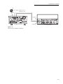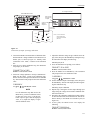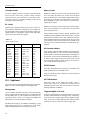
1
Model 6517A
Electrometer
Service Manual
References to the Model 6517 also apply to the Model 6517A.
Contains Performance Verification, Calibration, and Repair Information
WARRANTY
Keithley Instruments, Inc. warrants this product to be free from defects in material and workmanship for a period of 1 year from
date of shipment.
Keithley Instruments, Inc. warrants the following items for 90 days from the date of shipment: probes, cables, rechargeable batteries, diskettes, and documentation.
During the warranty period, we will, at our option, either repair or replace any product that proves to be defective.
To exercise this warranty, write or call your local Keithley representative, or contact Keithley headquarters in Cleveland, Ohio. You
will be given prompt assistance and return instructions. Send the product, transportation prepaid, to the indicated service facility.
Repairs will be made and the product returned, transportation prepaid. Repaired or replaced products are warranted for the balance
of the original warranty period, or at least 90 days.
LIMITATION OF WARRANTY
This warranty does not apply to defects resulting from product modification without Keithley’s express written consent, or misuse
of any product or part. This warranty also does not apply to fuses, software, non-rechargeable batteries, damage from battery leakage, or problems arising from normal wear or failure to follow instructions.
THIS WARRANTY IS IN LIEU OF ALL OTHER WARRANTIES, EXPRESSED OR IMPLIED, INCLUDING ANY IMPLIED
WARRANTY OF MERCHANTABILITY OR FITNESS FOR A PARTICULAR USE. THE REMEDIES PROVIDED HEREIN
ARE BUYER’S SOLE AND EXCLUSIVE REMEDIES.
NEITHER KEITHLEY INSTRUMENTS, INC. NOR ANY OF ITS EMPLOYEES SHALL BE LIABLE FOR ANY DIRECT,
INDIRECT, SPECIAL, INCIDENTAL OR CONSEQUENTIAL DAMAGES ARISING OUT OF THE USE OF ITS INSTRUMENTS AND SOFTWARE EVEN IF KEITHLEY INSTRUMENTS, INC., HAS BEEN ADVISED IN ADVANCE OF THE POSSIBILITY OF SUCH DAMAGES. SUCH EXCLUDED DAMAGES SHALL INCLUDE, BUT ARE NOT LIMITED TO: COSTS
OF REMOVAL AND INSTALLATION, LOSSES SUSTAINED AS THE RESULT OF INJURY TO ANY PERSON, OR DAMAGE TO PROPERTY.
Keithley Instruments, Inc. • 28775 Aurora Road • Cleveland, OH 44139 • 440-248-0400 • Fax: 440-248-6168 • http://www.keithley.com
BELGIUM:
CHINA:
FRANCE:
GERMANY:
GREAT BRITAIN:
INDIA:
ITALY:
NETHERLANDS:
SWITZERLAND:
TAIWAN:
Keithley Instruments B.V.
Keithley Instruments China
Keithley Instruments Sarl
Keithley Instruments GmbH
Keithley Instruments Ltd
Keithley Instruments GmbH
Keithley Instruments s.r.l.
Keithley Instruments B.V.
Keithley Instruments SA
Keithley Instruments Taiwan
Bergensesteenweg 709 • B-1600 Sint-Pieters-Leeuw • 02/363 00 40 • Fax: 02/363 00 64
Yuan Chen Xin Building, Room 705 • 12 Yumin Road, Dewai, Madian • Beijing 100029 • 8610-62022886 • Fax: 8610-62022892
B.P. 60 • 3, allée des Garays • 91122 Palaiseau Cédex • 01 64 53 20 20 • Fax: 01 60 11 77 26
Landsberger Strasse 65 • D-82110 Germering • 089/84 93 07-40 • Fax: 089/84 93 07-34
The Minster • 58 Portman Road • Reading, Berkshire RG30 1EA • 0118-9 57 56 66 • Fax: 0118-9 59 64 69
Flat 2B, WILOCRISSA • 14, Rest House Crescent • Bangalore 560 001 • 91-80-509-1320/21 • Fax: 91-80-509-1322
Viale S. Gimignano, 38 • 20146 Milano • 02/48 30 30 08 • Fax: 02/48 30 22 74
Postbus 559 • 4200 AN Gorinchem • 0183-635333 • Fax: 0183-630821
Kriesbachstrasse 4 • 8600 Dübendorf • 01-821 94 44 • Fax: 01-820 30 81
1 Fl. 85 Po Ai Street • Hsinchu, Taiwan, R.O.C. • 886-3572-9077• Fax: 886-3572-9031
6/99
Model 6517A Electrometer
Service Manual
©1998, Keithley Instruments, Inc.
All rights reserved.
Cleveland, Ohio, U.S.A.
Second Printing, April 1999
Document Number: 6517A-902-01 Rev. B
Manual Print History
The print history shown below lists the printing dates of all Revisions and Addenda created for this manual. The Revision
Level letter increases alphabetically as the manual undergoes subsequent updates. Addenda, which are released between Revisions, contain important change information that the user should incorporate immediately into the manual. Addenda are numbered sequentially. When a new Revision is created, all Addenda associated with the previous Revision of the manual are
incorporated into the new Revision of the manual. Each new Revision includes a revised copy of this print history page.
Revision A (Document Number 6517A-902-01)............................................................................ September 1998
Revision B (Document Number 6517A-902-01)..................................................................................... April 1999
All Keithley product names are trademarks or registered trademarks of Keithley Instruments, Inc.
Other brand and product names are trademarks or registered trademarks of their respective holders.
Safety Precautions
The following safety precautions should be observed before using
this product and any associated instrumentation. Although some instruments and accessories would normally be used with non-hazardous voltages, there are situations where hazardous conditions
may be present.
This product is intended for use by qualified personnel who recognize shock hazards and are familiar with the safety precautions required to avoid possible injury. Read the operating information
carefully before using the product.
The types of product users are:
Responsible body is the individual or group responsible for the use
and maintenance of equipment, for ensuring that the equipment is
operated within its specifications and operating limits, and for ensuring that operators are adequately trained.
Operators use the product for its intended function. They must be
trained in electrical safety procedures and proper use of the instrument. They must be protected from electric shock and contact with
hazardous live circuits.
Maintenance personnel perform routine procedures on the product
to keep it operating, for example, setting the line voltage or replacing consumable materials. Maintenance procedures are described in
the manual. The procedures explicitly state if the operator may perform them. Otherwise, they should be performed only by service
personnel.
Service personnel are trained to work on live circuits, and perform
safe installations and repairs of products. Only properly trained service personnel may perform installation and service procedures.
Exercise extreme caution when a shock hazard is present. Lethal
voltage may be present on cable connector jacks or test fixtures. The
American National Standards Institute (ANSI) states that a shock
hazard exists when voltage levels greater than 30V RMS, 42.4V
peak, or 60VDC are present. A good safety practice is to expect
that hazardous voltage is present in any unknown circuit before
measuring.
Users of this product must be protected from electric shock at all
times. The responsible body must ensure that users are prevented
access and/or insulated from every connection point. In some cases,
connections must be exposed to potential human contact. Product
users in these circumstances must be trained to protect themselves
from the risk of electric shock. If the circuit is capable of operating
at or above 1000 volts, no conductive part of the circuit may be
exposed.
As described in the International Electrotechnical Commission
(IEC) Standard IEC 664, digital multimeter measuring circuits
(e.g., Keithley Models 175A, 199, 2000, 2001, 2002, and 2010) are
Installation Category II. All other instruments’ signal terminals are
Installation Category I and must not be connected to mains.
Do not connect switching cards directly to unlimited power circuits.
They are intended to be used with impedance limited sources.
NEVER connect switching cards directly to AC mains. When connecting sources to switching cards, install protective devices to limit fault current and voltage to the card.
Before operating an instrument, make sure the line cord is connected to a properly grounded power receptacle. Inspect the connecting
cables, test leads, and jumpers for possible wear, cracks, or breaks
before each use.
For maximum safety, do not touch the product, test cables, or any
other instruments while power is applied to the circuit under test.
ALWAYS remove power from the entire test system and discharge
any capacitors before: connecting or disconnecting cables or jumpers, installing or removing switching cards, or making internal
changes, such as installing or removing jumpers.
Do not touch any object that could provide a current path to the
common side of the circuit under test or power line (earth) ground.
Always make measurements with dry hands while standing on a
dry, insulated surface capable of withstanding the voltage being
measured.
The instrument and accessories must be used in accordance with its
specifications and operating instructions or the safety of the equipment may be impaired.
The WARNING heading in a manual explains dangers that might
result in personal injury or death. Always read the associated information very carefully before performing the indicated procedure.
Do not exceed the maximum signal levels of the instruments and accessories, as defined in the specifications and operating information, and as shown on the instrument or test fixture panels, or
switching card.
The CAUTION heading in a manual explains hazards that could
damage the instrument. Such damage may invalidate the warranty.
When fuses are used in a product, replace with same type and rating
for continued protection against fire hazard.
Before performing any maintenance, disconnect the line cord and
all test cables.
Chassis connections must only be used as shield connections for
measuring circuits, NOT as safety earth ground connections.
If you are using a test fixture, keep the lid closed while power is applied to the device under test. Safe operation requires the use of a
lid interlock.
If a
screw is present, connect it to safety earth ground using the
wire recommended in the user documentation.
The ! symbol on an instrument indicates that the user should refer to the operating instructions located in the manual.
The
symbol on an instrument shows that it can source or measure 1000 volts or more, including the combined effect of normal
and common mode voltages. Use standard safety precautions to
avoid personal contact with these voltages.
Instrumentation and accessories shall not be connected to humans.
To maintain protection from electric shock and fire, replacement
components in mains circuits, including the power transformer, test
leads, and input jacks, must be purchased from Keithley Instruments. Standard fuses, with applicable national safety approvals,
may be used if the rating and type are the same. Other components
that are not safety related may be purchased from other suppliers as
long as they are equivalent to the original component. (Note that selected parts should be purchased only through Keithley Instruments
to maintain accuracy and functionality of the product.) If you are
unsure about the applicability of a replacement component, call a
Keithley Instruments office for information.
To clean an instrument, use a damp cloth or mild, water based
cleaner. Clean the exterior of the instrument only. Do not apply
cleaner directly to the instrument or allow liquids to enter or spill
on the instrument. Products that consist of a circuit board with no
case or chassis (e.g., data acquisition board for installation into a
computer) should never require cleaning if handled according to instructions. If the board becomes contaminated and operation is affected, the board should be returned to the factory for proper
cleaning/servicing.
Rev. 2/99
Table of Contents
1
Performance Verification
1.1
1.2
1.3
1.4
1.5
1.5.1
1.5.2
1.5.3
1.5.4
1.6
1.7
1.8
1.8.1
1.8.2
1.9
1.9.1
1.9.2
1.9.3
1.9.4
1.10
1.11
1.12
Introduction ....................................................................................................................................................... 1-1
Environmental conditions ................................................................................................................................. 1-1
Warm-up period ................................................................................................................................................ 1-2
Line power ........................................................................................................................................................ 1-2
Recommended test equipment .......................................................................................................................... 1-2
Meter performance verification equipment ............................................................................................... 1-2
Voltage source verification equipment ..................................................................................................... 1-3
Temperature verification equipment ......................................................................................................... 1-3
Humidity verification equipment .............................................................................................................. 1-4
Verification limits ............................................................................................................................................. 1-4
Restoring default conditions ............................................................................................................................. 1-4
Offset voltage and bias current calibration ....................................................................................................... 1-5
Front panel offset calibration .................................................................................................................... 1-5
IEEE-488 bus offset calibration ................................................................................................................ 1-5
Meter verification procedures ........................................................................................................................... 1-5
DC volts verification ................................................................................................................................. 1-6
DC amps verification ................................................................................................................................ 1-6
Coulombs verification ............................................................................................................................... 1-9
Ohms verification .................................................................................................................................... 1-11
Voltage source verification ............................................................................................................................. 1-14
Temperature verification ................................................................................................................................. 1-15
Humidity verification ...................................................................................................................................... 1-16
2
Calibration
2.1
2.2
2.3
2.4
2.5
2.6
2.6.1
2.6.2
2.7
2.7.1
2.7.2
2.8
2.8.1
2.8.2
2.9
Introduction ....................................................................................................................................................... 2-1
Environmental conditions ................................................................................................................................. 2-2
Warm-up period ................................................................................................................................................ 2-2
Line power ........................................................................................................................................................ 2-2
Recommended calibration equipment ............................................................................................................... 2-2
Calibration lock ................................................................................................................................................. 2-4
Unlocking calibration ................................................................................................................................ 2-4
IEEE-488 bus calibration lock status ........................................................................................................ 2-4
Calibration errors .............................................................................................................................................. 2-4
Front panel error reporting ........................................................................................................................ 2-4
IEEE-488 bus error reporting .................................................................................................................... 2-4
Front panel calibration ...................................................................................................................................... 2-4
Front panel calibration summary .............................................................................................................. 2-4
Front panel calibration procedure ............................................................................................................. 2-6
IEEE-488 bus calibration ................................................................................................................................ 2-15
i
2.9.1
2.9.2
2.10
2.10.1
2.10.2
2.11
Calibration commands ............................................................................................................................. 2-15
IEEE-488 bus comprehensive calibration procedure .............................................................................. 2-15
Single-point calibration ................................................................................................................................... 2-21
Front panel single-point calibration ......................................................................................................... 2-21
IEEE-488 bus single-point calibration .................................................................................................... 2-22
Programming calibration dates ........................................................................................................................ 2-23
3
Calibration Command Reference
3.1
3.2
3.3
3.3.1
3.3.2
3.3.3
3.3.4
3.3.5
3.3.6
3.3.7
3.3.8
3.3.9
3.4
3.4.1
3.4.2
3.4.3
3.4.4
3.5
3.6
3.7
3.8
3.8.1
3.8.2
3.9
3.9.1
3.9.2
3.9.3
Introduction ....................................................................................................................................................... 3-1
Command summary ........................................................................................................................................... 3-1
Miscellaneous commands .................................................................................................................................. 3-5
:INIT (:CALibration:PROTected:INITiate) .............................................................................................. 3-5
:LOCK (:CALibration:PROTected:LOCK) .............................................................................................. 3-5
:SWITch? (:CALibration:PROTected:SWITch?) ..................................................................................... 3-6
:SAVE (:CALibration:PROTected:SAVE) ............................................................................................... 3-6
:DATE (:CALibration:PROTected:DATE) ............................................................................................... 3-7
:NDUE (:CALibration:PROTected:NDUE) .............................................................................................. 3-7
:DATA? (:CALibration:PROTected:DATA?) .......................................................................................... 3-8
:OPT? (:CALibration:UNPRotected:OPTion?) ......................................................................................... 3-8
:CALTEMP (:CALibration:PROTected:CALTEMP) ................................................................................3-8
Meter commands ............................................................................................................................................... 3-9
Offset commands ....................................................................................................................................... 3-9
Volts function calibration commands ...................................................................................................... 3-10
Amps calibration commands ................................................................................................................... 3-11
Coulombs calibration commands ............................................................................................................ 3-13
Voltage source calibration commands ............................................................................................................. 3-15
Temperature calibration commands ................................................................................................................ 3-16
Humidity calibration commands ..................................................................................................................... 3-16
Calibration errors ............................................................................................................................................. 3-17
Error query commands ............................................................................................................................ 3-17
Detecting calibration errors ..................................................................................................................... 3-18
Detecting calibration step completion ............................................................................................................. 3-18
Using the *OPC? query ........................................................................................................................... 3-18
Using the *OPC command ...................................................................................................................... 3-18
Generating an SRQ on calibration complete ........................................................................................... 3-18
4
Routine Maintenance
4.1
4.2
4.3
4.4
4.5
Introduction ........................................................................................................................................................ 4-1
Line voltage selection ......................................................................................................................................... 4-1
Line fuse replacement ......................................................................................................................................... 4-1
INPUT connector cleaning ................................................................................................................................. 4-2
Firmware updates ............................................................................................................................................... 4-2
ii
5
Troubleshooting
5.1
5.2
5.3
5.4
5.4.1
5.4.2
5.4.3
5.5
5.5.1
5.5.2
5.5.3
5.5.4
5.6
5.6.1
5.6.2
5.6.3
5.6.4
Introduction ........................................................................................................................................................ 5-1
Repair considerations ......................................................................................................................................... 5-1
Power-on test ...................................................................................................................................................... 5-2
Front panel tests ................................................................................................................................................. 5-2
KEYS test ................................................................................................................................................... 5-2
DISPLAY PATTERNS test ....................................................................................................................... 5-2
Character set test ........................................................................................................................................ 5-2
Principles of operation ....................................................................................................................................... 5-2
Display board ............................................................................................................................................. 5-4
Power supply .............................................................................................................................................. 5-4
Digital board .............................................................................................................................................. 5-6
Analog board .............................................................................................................................................. 5-7
Circuit board checks ......................................................................................................................................... 5-10
Display board checks ............................................................................................................................... 5-10
Power supply checks ................................................................................................................................ 5-11
Digital board checks ................................................................................................................................. 5-12
Analog board checks ................................................................................................................................ 5-13
6
Disassembly
6.1
6.2
6.2.1
6.2.2
6.3
6.4
6.5
6.5.1
6.5.2
6.5.3
6.6
6.7
6.8
6.9
Introduction ........................................................................................................................................................
Handling and cleaning precautions ....................................................................................................................
PC board handling ......................................................................................................................................
Solder repairs .............................................................................................................................................
Special handling of static-sensitive devices .......................................................................................................
Case cover removal ............................................................................................................................................
PC board removal ...............................................................................................................................................
Digital board removal ................................................................................................................................
A/D converter board removal .....................................................................................................................
Analog board removal ................................................................................................................................
Front panel disassembly .....................................................................................................................................
Main CPU firmware replacement ......................................................................................................................
Instrument re-assembly ......................................................................................................................................
Assembly drawings ............................................................................................................................................
7
Replaceable Parts
7.1
7.2
7.3
7.4
7.5
Introduction ........................................................................................................................................................
Parts lists ............................................................................................................................................................
Ordering information .........................................................................................................................................
Factory service ...................................................................................................................................................
Component layouts ............................................................................................................................................
A
Specifications
B
Calibration Messages
C
Calibration Command Summary
6-1
6-1
6-1
6-2
6-2
6-2
6-2
6-3
6-3
6-3
6-4
6-4
6-5
6-5
7-1
7-1
7-1
7-1
7-1
iii
List of Illustrations
1
Performance Verification
Figure 1-1
Figure 1-2
Figure 1-3
Figure 1-4
Figure 1-5
Figure 1-6
Figure 1-7
Figure 1-8
Figure 1-9
Figure 1-10
Figure 1-11
Connections for DC volts verification ....................................................................................................... 1-7
Connections for 20pA–2µA range verification .......................................................................................... 1-7
Connections for 20µA–20mA range verification ....................................................................................... 1-9
Connections for coulombs verification .................................................................................................... 1-10
Connections for ohms verification (2MΩ–200MΩ ranges) ..................................................................... 1-12
Connections for ohms verification (2GΩ–200GΩ ranges) ...................................................................... 1-13
Connections for ohms verification (2TΩ–200TΩ ranges) ....................................................................... 1-14
Shielded fixture construction ................................................................................................................... 1-14
Connections for voltage source verification ............................................................................................ 1-15
Connections for temperature verification ................................................................................................. 1-16
Connections for humidity verification ..................................................................................................... 1-17
2
Calibration
Figure 2-1
Figure 2-2
Figure 2-3
Figure 2-4
Figure 2-5
Figure 2-6
Figure 2-7
Figure 2-8
Calibration unit connections ...................................................................................................................... 2-7
Connections for DC volts calibration ......................................................................................................... 2-8
Connections for 20pA–2µA range calibration ........................................................................................... 2-9
Connections for 20µA–20mA range calibration ...................................................................................... 2-10
Connections for coulombs calibration ..................................................................................................... 2-11
Connections for temperature calibration .................................................................................................. 2-12
Connections for voltage source calibration .............................................................................................. 2-13
Connections for humidity calibration ...................................................................................................... 2-14
4
Routine Maintenance
Figure 4-1
Rear panel .................................................................................................................................................. 4-2
5
Troubleshooting
Figure 5-1
Figure 5-2
Figure 5-3
Figure 5-4
Figure 5-5
Figure 5-6
Model 6517A overall block diagram .........................................................................................................
Display board block diagram .....................................................................................................................
Power supply block diagram ......................................................................................................................
Digital board block digram ........................................................................................................................
Analog board block diagram ......................................................................................................................
Preamp configurations ...............................................................................................................................
5-3
5-4
5-5
5-7
5-8
5-9
v
B
Calibration Messages
Figure B-1
Figure B-2
Figure B-3
Figure B-4
Figure B-5
Figure B-6
Figure B-7
Figure B-8
EERR? query response (calibration execution errors) ..............................................................................
VERR? query response (voltage function cal errors) ................................................................................
IERR? query response (current function cal errors) ..................................................................................
CERR? query response (coulombs function cal errors) ............................................................................
TERR? query response (temperature function cal errors) .........................................................................
HERR? query response (humidity function cal errors) .............................................................................
SERR? query response (voltage source cal errors) ...................................................................................
FERR? query response (factor cal errors) .................................................................................................
vi
B-6
B-6
B-6
B-7
B-7
B-7
B-7
B-7
List of Tables
1
Performance Verification
Table 1-1
Table 1-2
Table 1-3
Table 1-4
Table 1-5
Table 1-6
Table 1-7
Table 1-8
Table 1-9
Table 1-10
Table 1-11
Table 1-12
Recommended test equipment for meter performance verification ........................................................... 1-3
Recommended test equipment for voltage source verification .................................................................. 1-3
Temperature verification equipment .......................................................................................................... 1-3
Humidity verification equipment ............................................................................................................... 1-4
Limits for DC volts verification ................................................................................................................. 1-6
Reading limits for verification of 20pA-2µA ranges ................................................................................. 1-8
Limits for 20µA–20mA range verification ................................................................................................ 1-9
Limits for coulombs verification .............................................................................................................. 1-10
Limits for ohms verification .................................................................................................................... 1-12
Limits for voltage source verification ...................................................................................................... 1-15
Reading limits for temperature verification ............................................................................................. 1-15
Limits for humidity verification ............................................................................................................... 1-16
2
Calibration
Table 2-1
Table 2-2
Table 2-3
Table 2-4
Table 2-5
Table 2-6
Table 2-7
Table 2-8
Table 2-9
Table 2-10
Table 2-11
Table 2-12
Table 2-13
Table 2-14
Table 2-15
Recommended calibration equipment ........................................................................................................ 2-3
Front panel calibration summary ............................................................................................................... 2-5
Volts calibration summary ......................................................................................................................... 2-8
Amps calibration summary (20pA–2µA ranges) ..................................................................................... 2-10
Amps calibration summary (20µA-20mA ranges) ................................................................................... 2-10
Coulombs calibration summary ............................................................................................................... 2-12
Voltage source calibration summary ........................................................................................................ 2-13
Humidity calibration summary ................................................................................................................ 2-14
Offset calibration steps ............................................................................................................................. 2-15
IEEE-488 bus volts function calibration summary .................................................................................. 2-16
IEEE-488 bus amps calibration summary (20pA-2µA ranges) ............................................................... 2-18
IEEE-488 bus amps calibration summary (20µA-20mA ranges) ............................................................ 2-18
IEEE-488 bus coulombs calibration summary ......................................................................................... 2-19
IEEE-488 bus voltage source calibration summary ................................................................................. 2-20
IEEE-488 bus humidity calibration summary .......................................................................................... 2-21
vii
3
Calibration Command Reference
Table 3-1
Table 3-2
Table 3-3
Table 3-4
Table 3-5
Table 3-6
Table 3-7
IEEE-488 bus calibration command summary ........................................................................................... 3-2
Volts function calibration commands and parameters ............................................................................. 3-10
Amps function calibration commands and parameters (all ranges, without calibration standard) .......... 3-11
Amps function calibration commands and parameters (20pA-2µA ranges, using calibration standard). 3-12
Coulombs function calibration commands and parameters (without calibration standard) ..................... 3-13
Coulombs function calibration commands and parameters (using calibration standard) ......................... 3-14
Voltage source calibration commands ...................................................................................................... 3-15
4
Routine Maintenance
Table 4-1
Power line fuse ........................................................................................................................................... 4-2
5
Troubleshooting
Table 5-1
Table 5-2
Table 5-3
Table 5-4
Table 5-5
Power supply circuits ................................................................................................................................ 5-6
Display board checks ................................................................................................................................ 5-10
Power supply checks ................................................................................................................................ 5-11
Digital board checks ................................................................................................................................. 5-12
Analog board checks ................................................................................................................................ 5-13
7
Replaceable Parts
Table 7-1
Table 7-2
Table 7-3
Table 7-4
Table 7-5
Table 7-6
Model 6517A ADC board, parts list ........................................................................................................... 7-2
Model 6517A display board, parts list ....................................................................................................... 7-5
Model 6517A analog board, parts list ........................................................................................................ 7-6
Model 6517A digital board, parts list ....................................................................................................... 7-10
Model 6517A mechanical board, parts list ............................................................................................... 7-12
Model 6517A miscellaneous parts list ..................................................................................................... 7-13
B
Calibration Messages
Table B-1
Table B-2
Table B-3
Calibration error responses ........................................................................................................................ B-2
Calibration error query commands ............................................................................................................ B-4
Calibration constants returned by :CAL:PROT:DATA? query ................................................................ B-5
C
Calibration Command Summary
Table C-1
Calibration commands ............................................................................................................................... C-1
viii
1
Performance Verification
1.1
Introduction
The procedures in this section are intended to verify that
Model 6517A accuracy is within the limits stated in the
instrument one-year accuracy specifications. These procedures can be performed when the instrument is first received
to ensure that no damage has occurred during shipment. Verification may also be performed whenever there is a question
of instrument accuracy, or following calibration, if desired.
1.4
Line power: Covers power line voltage ranges during
testing.
1.5
Recommended equipment: Summarizes recommended test equipment and pertinent specifications.
1.6
Verification limits: Explains how reading limits were
calculated.
1.7
Restoring default conditions: Gives step-by-step
procedures for restoring default conditions before
each test procedure.
1.8
Offset voltage and bias current calibration: Covers
methods to null offset voltage and bias current.
1.9
Meter verification procedures: Details procedures to
verify accuracy of Model 6517A measurement functions: volts, amps, coulombs, and ohms.
WARNING
The information in this section is
intended for use only by qualified service personnel. Do not attempt these
procedures unless you are qualified to
do so.
NOTE
If the instrument is still under warranty,
and its performance is outside specified
limits, contact your Keithley representative or the factory to determine the correct
course of action.
1.10 Voltage source verification: Covers verifying voltage
source output accuracy.
1.11 Temperature verification: Explains how to check
temperature measurement accuracy.
1.12 Humidity verification: Summarizes the basic procedure to check humidity measurement accuracy.
This section includes the following:
1.2
Environmental conditions
1.2
Environmental conditions: Covers the temperature
and humidity limits for verification.
1.3
Warm-up period: Describes the length of time the
Model 6517A should be allowed to warm up before
testing.
Verification measurements should be made at an ambient
temperature of 18° to 28°C (65° to 82°F), and at a relative
humidity of less than 70% unless otherwise noted.
1-1
Performance Verification
1.3
Warm-up period
The Model 6517A must be allowed to warm up for at least
one hour before performing the verification procedures. If
the instrument has been subjected to temperature extremes
(outside the range stated in paragraph 1.2), allow additional
time for internal temperatures to stabilize. Typically, it takes
one additional hour to stabilize a unit that has been in an
environment 10°C (18°F) above or below the specified temperature range.
The test equipment should also be allowed to warm up for
the minimum period specified by the manufacturer.
1.4
Line power
The Model 6517A should be tested while operating from a
line voltage within the range determined by the rear panel
LINE VOLTAGE switch setting, at a frequency of 50 or
60Hz.
1.5
Recommended test equipment
The following paragraphs list test equipment recommended
for performing the verification procedures for the various
Model 6517A functions. Alternate equipment may be used
as long as that equipment has specifications comparable to or
better than those listed in the table.
NOTE
Make all input low connections directly to
the triax INPUT connector instead of using COMMON to avoid internal voltage
drops that could affect measurement accuracy. Use the connecting methods shown
in this section to avoid this problem.
1-2
1.5.1 Meter performance verification equipment
Table 1-1 lists all test equipment required for verifying the
measurement accuracy of Model 6517A meter functions.
This equipment will allow you to check the accuracy of the
instrument volts, amps, and coulombs functions.
NOTE
The Model 5156 Electrometer Calibration
Standard is recommended for verifying
accuracy of the 20pA-2µA amps ranges, the
2GΩ-200GΩ resistance ranges, and all coulombs ranges. Alternate resistance and
capacitance standards may be substituted as
long as those standards are characterized to
an uncertainty at least four times better than
equivalent Model 6517A specifications.
NOTE
The ohms function and its accuracy are
derived from the voltage source and current
measurement function and their respective
specifications. If both the voltage source and
current measurement function meet their
accuracy specifications, it is not necessary to
independently verify ohms function
accuracy. The ohms verification procedure in
this manual (paragraph 1.9.4) is provided for
those who require Artifact Standard
Verification. Because of limitations in highvalue
standard
resistor
accuracy,
characterized resistors are required in
addition to the Model 5156 Electrometer
Calibration Standard.
Performance Verification
Table 1-1
Recommended test equipment for meter performance verification
Mfg.
Model
Description
Specifications
Fluke
5700A
Calibrator
Keithley
5156
Electrometer Calibration Standard
±5ppm basic uncertainty.1
DC Voltage:
1.9V: ±7ppm
19V: ±5ppm
190V:±7ppm
DC current:
19µA: ±576ppm
190µA: ±103ppm
1.9mA: ±55ppm
19mA: ±55ppm
Ohms:
1.9MΩ (nominal)
19MΩ (nominal)
100MΩ (nominal)
100MΩ2 [2µA, 200nA]
1GΩ [2nA, 20nA, 2GΩ]
10GΩ [200pA, 20GΩ]
100GΩ [20pA, 200GΩ]
1nF [2nC, 20nC]
100nF [200nC, 2µC]
1TΩ3
10TΩ
100TΩ
Characterized resistors
(Artifact Verification Only)
Keithley
Keithley
4801
7078-TRX-BNC
Keithley
Keithley
237-ALG-2
CAP-31
Low-noise coax cable
Triax-to BNC adapter
BNC to dual banana plug adapter
Triax to alligator clip cable*
Triax shielding cap
1. 90-day calibrator specifications shown include total absolute uncertainty at specified output.
2. Equivalent resistance and capacitance standards may be substituted if characterized to four times better uncertainty than
equivalent Model 6517A specifications.
3. Resistors must be characterized to four times better uncertainty than equivalent Model 6517A specifications.
*Short red and black clips to make triax short.
1.5.2 Voltage source verification equipment
1.5.3 Temperature verification equipment
Table 1-2 summarizes equipment recommended to perform
voltage source verification.
Table 1-3 lists temperature verification equipment.
Table 1-2
Recommended test equipment for voltage source verification
Mfg.
Model Description
Keithley 2001
Multimeter
Keithley 8607
Dual banana
plug cable
Specifications*
200V range: ±41ppm
1000V range: ±47ppm
Table 1-3
Temperature verification equipment
Mfg.
Model
Description
Omega CL-307K Type K Thermocouple Calibrator/
Simulator
Specifications
-190°C to
+1300°C, ±0.4%
*1-year multimeter specifications are for full-range input.
1-3
Performance Verification
1.5.4 Humidity verification equipment
Table 1-4 summarizes test equipment recommended to verify the accuracy of the Model 6517A humidity measurement
function.
• Model 6517A 200µA range one-year accuracy: ±(0.1%
of reading + 5 counts)
• Calibrator total absolute uncertainty at 190µA output:
±103ppm
The calculated limits are:
Table 1-4
Humidity verification equipment
Mfg.
Model Description
Specifications*
Fluke
5700A DC voltage calibrator 0V, 0.5V, 1V,
±5ppm basic
accuracy
Reading limits = 190µA ± [(190µA × 0.1% + 0.005µA) +
(190µA × 103ppm)]
Reading limits = 190µA ± 0.21457µA
Reading limits = 189.7854µA to 190.2146µA
Banana plugs to clip
leads
1.7
2, 1 in. lengths of
solid #20AWG wire
Before performing each performance verification procedure,
restore instrument bench default conditions as follows:
* DC voltage calibrator with better than 0.25% basic accuracy may be
substituted.
Restoring default conditions
1. From the normal display mode, press the MENU key.
The instrument will display the following:
MAIN MENU
1.6
Verification limits
The verification limits stated in this section have been calculated using only Model 6517A one-year accuracy specifications, and do not include test equipment uncertainty. In cases
where the Model 6517A apparently does not meet its published specifications based on stated reading limits, reading
limits should be recalculated using both Model 6517A accuracy specifications and the total absolute uncertainty of the
verification equipment.
Reading limit calculation example
As an example of how reading limits can be calculated using
test equipment uncertainty, assume that the 200µA range is
being tested using a 190µA input value, and the various specifications are as follows:
1-4
SAVESETUP
COMMUNICATION
CAL
2. Select SAVESETUP, and press ENTER. The following
will be displayed:
SETUP MENU
SAVE
RESTORE
POWERON
RESET
3. Select RESET, and press ENTER. The display will then
appear as follows:
RESET ORIGINAL DFLTS
BENCH
GPIB
4. Select BENCH, then press ENTER. The following will
be displayed:
RESETTING INSTRUMENT
ENTER to confirm; EXIT to abort
5. Press ENTER again to confirm instrument reset. The
instrument will return to normal display with bench
defaults restored.
Performance Verification
1.8
Offset voltage and bias current
calibration
Before performing meter verification procedures (checking
accuracy of the volts, amps, coulombs, and ohms measurement functions), the offset voltage and bias current calibration procedure should be performed, as described in the
following paragraphs.
1.8.1 Front panel offset calibration
To calibrate voltage offset and input bias current from the
front panel, proceed as follows:
1. Turn on the Model 6517A, and allow a one-hour warmup period before calibrating offsets.
2. From normal display, press the MENU key.
3. Select CAL, then press ENTER.
4. Choose OFFSET-ADJ, then press ENTER. The instrument will prompt you as follows:
Wait until the instrument completes this step before continuing.
3. Removing the triax shorting cable, and connect the triax
shielding (non-shorting) cap in its place.
4. Send the following command to the instrument over the
IEEE-488 bus:
:CAL:UNPR:IOFF
5. Wait until the instrument completes bias current calibration, then remove the cap from the rear panel INPUT
connector.
1.9
Meter verification procedures
The following paragraphs contain procedures for verifying
instrument one-year accuracy specifications for the following functions:
• DC volts
• DC amps
CONNECT TRIAX SHORT
• Coulombs
Press ENTER to continue.
• Ohms
5. Connect the shorted triax cable (short red and black
clips) to the rear panel INPUT connector, then press
ENTER. The instrument will then perform voltage offset calibration, during which it will display the following message:
Performing V offset calibration
6. The Model 6517A will then prompt you as follows:
CONNECT TRIAX CAP
Press ENTER to continue
7. Removing the triax short, and connect the triax shielding (non-shorting) cap in its place.
8. Press ENTER. The Model 6517A will perform offset
current verification, during which it will display the following message:
NOTE
Ohms accuracy specifications are derived
from both amps and voltage source specifications. Thus, it is not necessary to separately verify the accuracy of the ohms
function. As long as the amps function and
voltage source meet their respective accuracy specifications, ohms function accuracy is assured.
If the Model 6517A meter functions are out of specifications
and not under warranty, refer to the calibration procedures in
Section 2.
Performing I offset calibration
9. Press EXIT as necessary to return to normal display
once both offset calibration procedures are completed.
1.8.2 IEEE-488 bus offset calibration
To calibrate voltage offset and input bias current using IEEE488 bus commands, proceed as follows:
1. Turn on the Model 6517A, and allow a one-hour warmup period before calibrating voltage and current offsets.
2. Connect the triax shorting cable to the rear panel INPUT
connector, then send the following command over the
IEEE-488 bus:
WARNING
The maximum INPUT level (HI to LO)
is 250V peak. The maximum commonmode voltage is 500V peak.
Exceeding these values may cause damage to the unit.
Some of the procedures in this section
may expose you to hazardous voltages.
Use standard safety precautions when
such hazardous voltages are encountered to avoid personal injury caused by
electric shock.
:CAL:UNPR:VOFF
1-5
Performance Verification
NOTE
Do not connect test equipment to the
Model 6517A through a scanner or other
switching equipment.
1.9.1 DC volts verification
DC voltage accuracy is verified by applying accurate DC
voltages from a DC voltage calibrator to the Model 6517A
INPUT jack and verifying that the displayed readings fall
within specified ranges.
Follow the steps below to verify DCV measurement
accuracy.
1. Connect the Model 6517A to the calibrator, as shown in
Figure 1-1. Be sure to connect calibrator HI to Model
6517A INPUT HI and calibrator LO to the Model
6517A INPUT LO using the low-noise coax cable,
BNC-to-dual banana plug adapter, and the triax-to-BNC
adapter as shown.
2. Turn on the Model 6517A and the calibrator, and allow
a one-hour warm-up period before making
measurements.
3. Restore Model 6517A factory default conditions, as
explained in paragraph 1.7.
4. Select the Model 6517A 2V DC range, and make sure
the filter is enabled.
Table 1-5
Limits for DC volts verification
6517A
DCV
range
Applied DC
voltage
Reading limits
(18° to 28°C, 1 year)
2V
20V
200V
1.90000V
19.0000V
190.000V
1.89949V to 1.900515V
18.9950V to 19.0050V
189.883V to 190.117V
1. Repeat procedure for negative voltages of same magnitude.
2. Reading limits shown are calculated only from Model 6517A oneyear accuracy specifications and do not include test equipment
uncertainty.
1.9.2 DC amps verification
DC amps accuracy is checked by applying accurate DC currents to the instrument INPUT jack and then verifying that
the current readings fall within appropriate limits. Note that
two separate current verification procedures are provided
because of the different equipment required. Basically, the
amps verification procedures are divided into the following
two groups:
• 20pA – 2µA range verification using a DC voltage calibrator and the Keithley Model 5156 Electrometer Calibration Sandard, which contains standard resistors.
• 20µA – 20mA range verification using a DC current
calibrator.
NOTE
Do not use auto-ranging for any of the verification tests because auto-range hysteresis may cause the Model 6517A to be on
an incorrect range.
5. With zero check enabled, press REL to zero correct the
instrument.
6. Set the calibrator output to 0.00000VDC, and disable
zero check. Allow the reading to settle completely
before continuing.
7. Enable the Model 6517A REL mode. Leave REL enabled for the remainder of the DC volts verification
tests.
8. Set the calibrator output to +1.90000VDC, and allow the
reading to settle.
9. Verify that the Model 6517A reading is within the limits
summarized in Table 1-5.
10. Repeat steps 8 and 9 for the 20V and 200V ranges using
the test voltages listed in Table 1-5.
11. Repeat the procedure for each of the ranges with negative voltages of the same magnitude as those listed in Table 1-5.
1-6
20pA–2µA range verification
Accuracy of the 20pA-2µA ranges is verified by applying
accurate currents derived from DC voltages and resistance
standards, and then checking the displayed readings against
calculated limits. Note that it is necessary to calculate reading limits for each range separately from the exact values of
the resistance standards supplied with those standards.
Follow the steps below to verify measurement accuracy of
the 20pA to 2µA ranges.
1. Connect the Model 6517A to the DC voltage calibrator
and the calibration standards box, as shown in Figure
1-2. Initially, make connections to the calibration standard using the 100GΩ resistor.
NOTE
It is not necessary to connect the calibration standard to the Model 6517A DIGITAL I/O port when performing the
verification procedures.
Performance Verification
Low-noise Coax BNC Cable
Input
Triax-to-BNC Adapter
WARNING:NO INTERNAL OPERATOR SERVICABLE PARTS,SERVICE BY QUALIFIED PERSONNEL ONLY.
1010V
PEAK
HI SELECTED
LINE VOLTAGE
LO
PREAMP OUT COMMON
250 PEAK
INPUT
2V ANALOG
OUTPUT
90-110V
105-125V
V SOURCE
750V
PEAK
250V PEAK
HUMIDITY
TEMP
TYPE K
EXT TRIG
IN
MADE
IN
U.S.A.
180-220V
210-250V
115V
!
LINE FUSE
SLOWBLOW
LINE RATING
50-60HZ
50VA MAX
AC ONLY
1/2A 90-125V
1/4A 180-250V
MTR COMP
OUT
IEEE-488
(CHANGE IEEE ADDRESS
WITH FRONT PANEL MENU)
RS232
OPTION SLOT
DIGITAL TRIG LINK
I/O
Calibrator
Output
!
INTERLOCK
CAUTION:FOR CONTINUED PROTECTION AGAINST FIRE HAZARD,REPLACE FUSE WITH SAME TYPE AND RATING.
BNC-to-dual
Banana Plug
Adapter (Connect
Cable Shield to
Output LO)
Model 6517 Electrometer
DC Voltage Calibrator
Figure 1-1
Connections for DC volts verification
DC Voltage Calibrator
Model 6517 Electrometer
WARNING:NO INTERNAL OPERATOR SERVICABLE PARTS,SERVICE BY QUALIFIED PERSONNEL ONLY.
1010V
PEAK
HI SELECTED
LINE VOLTAGE
LO
PREAMP OUT COMMON
250 PEAK
INPUT
2V ANALOG
OUTPUT
90-110V
105-125V
V SOURCE
750V
PEAK
250V PEAK
HUMIDITY
TEMP
TYPE K
EXT TRIG
IN
BNC-to-dual
Banana Plug
Adapter
MADE
IN
U.S.A.
180-220V
210-250V
115V
!
LINE FUSE
SLOWBLOW
LINE RATING
50-60HZ
50VA MAX
AC ONLY
1/2A 90-125V
1/4A 180-250V
MTR COMP
OUT
IEEE-488
(CHANGE IEEE ADDRESS
WITH FRONT PANEL MENU)
RS232
OPTION SLOT
DIGITAL TRIG LINK
I/O
Connect Cable
Shield to
Output LO
!
INTERLOCK
CAUTION:FOR CONTINUED PROTECTION AGAINST FIRE HAZARD,REPLACE FUSE WITH SAME TYPE AND RATING.
Low-noise
Coax Cable
Triax Cable
100GΩ
10GΩ
OUTPUT
1nF
1GΩ
Note: Connect Calibrator to
Appropriate Resistor,
Link Shield and Chassis.
!
100nF
100MΩ
Model 5156 Electrometer Calibration Standard
Figure 1-2
Connections for 20pA–2µA range verification
2. Turn on the Model 6517A and the DC calibrator, and
allow a one-hour warm-up period before making measurements.
3. Restore Model 6517A factory default conditions, as
explained in paragraph 1.7.
4. Select the amps function and the 20pA range on the
Model 6517A.
5. With zero check enabled, press REL to zero correct the
instrument.
6. Set the calibrator output to 0.0000V, then disable zero
check. Enable the REL mode to null offsets.
7. Record the actual resistance values (see Model 5156 calibration data) in the appropriate column of Table 1-6.
8. Calculate the actual calibration voltage from the desired
current and the actual value of the 100GΩ resistor as
determined from the calibration data as follows:
V = IR
Where: I = desired current applied to Model 6517A
V = actual voltage from DC voltage calibrator
R = actual value of calibration standard resistance
1-7
Performance Verification
After calculating the actual voltage values, record them
where indicated in Table 1-6.
9. Set the DC calibrator to the actual voltage.
10. Make sure the DC voltage calibrator is in operate.
11. Allow the reading to settle completely, then note the
reading on the Model 6517A display. Verify that the
reading is within the limits listed in Table 1-6.
12. Reverse the calibrator voltage polarity, then make sure
the magnitude of current reading is within limits.
13. Repeat steps 4 through 12 for the 200pA through 2µA
ranges using the appropriate DC voltage and standard
resistor listed in Table 1-6. For each range, be sure to:
• Compute the actual calibrator voltage.
• Set the DC voltage calibrator to the correct setting.
• Null offsets using REL.
• Make connections to the appropriate standard resistance in the calibration standard test box.
20µA – 20mA range verification
Measurement accuracy of the 20µA-20mA ranges is verified
by applying accurate currents from a DC current calibrator
and then verifying that the Model 6517A reading is within
specified limits.
Proceed as follows:
1. Connect the Model 6517A to the DC current calibrator
using the low-noise coax cable, triax-to-BNC adapter,
and BNC-to-dual banana plug adapter, as shown in Figure 1-3. Be sure to connect the calibrator output HI terminal to Model 6517A INPUT HI, and connect
calibrator output LO to Model 6517A INPUT LO.
2. Turn on the Model 6517A and the calibrator, and allow
a one-hour warm-up period before making
measurements.
3. Restore Model 6517A factory default conditions, as explained in paragraph 1.7.
4. Select the amps function and the 20µA range on the
Model 6517A.
5. With zero check enabled, press REL to zero correct the
instrument.
6. Set the calibrator output to 0.000µA then disable zero
check. Enable REL to null offsets.
7. Set the calibrator output to +19.0000µADC, and disable
Model 6517A zero check.
8. Allow the reading to settle, then verify that the Model
6517A reading is within the limits for the selected measurement range, as summarized in Table 1-7.
9. Repeat steps 5 through 8 for the remaining ranges and
currents listed in Table 1-7.
10. Repeat the procedure for each of the ranges with negative currents of the same magnitude as those listed in
Table 1-7.
Table 1-6
Reading limits for verification of 20pA-2µA ranges
6517A
range
Nominal Standard
voltage
resistor
value
value
20pA 1.9000V
200pA 1.9000V
2nA 1.9000V
20nA 1.9000V
200nA 19.0000V
2µA 190.000V
100GΩ
10GΩ
1GΩ
100MΩ
100MΩ
100MΩ
Actual
resistance
Applied
current
__________ Ω
__________ Ω
__________ Ω
__________ Ω
__________ Ω
__________ Ω
19pA
190pA
1.9nA
19nA
190nA
1.9µA
Actual
voltage*
_________
_________
_________
_________
_________
_________
Reading limits
(1 year, 18° to 28°C)
V
V
V
V
V
V
18.8070 to 19.1930pA
188.095 to 191.905pA
1.89590 to 1.91410nA
18.9615 to 19.0385nA
189.615 to 190.385nA
1.89800 to 1.90200µA
* Voltage calculated as follows: V = IR, where V is calibrator voltage, R is actual value of resistance standard, and I is desired applied
current.
1-8
Performance Verification
Low-noise Coax BNC Cable
Triax-to-BNC Adapter
WARNING:NO INTERNAL OPERATOR SERVICABLE PARTS,SERVICE BY QUALIFIED PERSONNEL ONLY.
1010V
PEAK
HI SELECTED
LINE VOLTAGE
LO
PREAMP OUT COMMON
250 PEAK
INPUT
90-110V
105-125V
V SOURCE
750V
PEAK
250V PEAK
HUMIDITY
TEMP
TYPE K
EXT TRIG
IN
MADE
IN
U.S.A.
180-220V
210-250V
115V
!
2V ANALOG
OUTPUT
LINE RATING
50-60HZ
50VA MAX
AC ONLY
LINE FUSE
SLOWBLOW
1/2A 90-125V
1/4A 180-250V
MTR COMP
OUT
IEEE-488
(CHANGE IEEE ADDRESS
WITH FRONT PANEL MENU)
RS232
OPTION SLOT
DIGITAL TRIG LINK
I/O
!
INTERLOCK
CAUTION:FOR CONTINUED PROTECTION AGAINST FIRE HAZARD,REPLACE FUSE WITH SAME TYPE AND RATING.
Model 6517 Electrometer
BNC-to-dual
Banana Plug
Adapter (Connect
Cable Shield to
Output LO)
DC Current Calibrator
Figure 1-3
Connections for 20µA–20mA range verification
Table 1-7
Limits for 20µA–20mA range verification
6517A Applied DC
range
current
20µA
200µA
2mA
20mA
19.0000µA
190.000µA
1.90000mA
19.0000mA
Reading limits
(1 year, 18° to 28°C)
18.9805µA to 19.0195µA
189.805µA to 190.195µA
1.89800mA to 1.90200mA
18.9805mA to 19.0195mA
1. Repeat procedure for negative currents.
2. Reading limits shown calculated only from Model 6517A one-year
accuracy specifications and do not include test equipment
uncertainty.
1.9.3 Coulombs verification
Coulombs verification is performed by applying accurately
known charge values derived from a voltage source and a
capacitor to the Model 6517A INPUT jack, and then verifying that Model 6517A readings fall within specified limits.
Follow the steps below to verify coulombs measurement accuracy.
1. Connect the Model 6517A to the calibration standard
then to the voltage calibrator, as shown in Figure 1-4.
Initially, make the connections to the 1nF capacitor.
2. Turn on the Model 6517A and the DC voltage calibrator,
and allow a one-hour warm-up period before making
measurements.
3. Restore Model 6517A factory default conditions, as
explained in paragraph 1.7. Also make sure that the offset-nulling procedure discussed in paragraph 1.8 has
been performed.
4. Select the coulombs function and the 2nC range on the
Model 6517A.
5. Compute the desired calibrator voltages as follows:
Q
V = ---C
Where: V = calibrator voltage in volts
Q = charge in coulombs
C = standard capacitance value in farads
After calculating the voltage values, enter them where
indicated in Table 1-8.
6. With zero check enabled, press REL to zero correct the
instrument.
7. Disable zero check, and set the voltage calibrator output
to 0.0000V.
8. Set the calibrator output to the calculated voltage. Allow
the reading to settle completely.
9. Compare the Model 6517A displayed reading with the
limits shown in Table 1-8.
10. Set the calibrator output to 0.000000V, and enable zero
check.
11. Repeat steps 5 through 10 for the remaining ranges
listed in Table 1-8. For each range, be sure to:
• Set the Model 6517A to the appropriate range.
• Make connections to the correct capacitor in the calibration standard.
• Set the calibrator to 0V with zero check disabled.
• Set the voltage calibrator to the calculated voltage
value.
• Compare the Model 6517A reading with the stated
reading limits.
1-9
Performance Verification
DC Voltage Calibrator
Model 6517 Electrometer
WARNING:NO INTERNAL OPERATOR SERVICABLE PARTS,SERVICE BY QUALIFIED PERSONNEL ONLY.
1010V
PEAK
HI SELECTED
LINE VOLTAGE
LO
PREAMP OUT COMMON
250 PEAK
INPUT
2V ANALOG
OUTPUT
90-110V
105-125V
V SOURCE
750V
PEAK
250V PEAK
HUMIDITY
TEMP
TYPE K
EXT TRIG
IN
MADE
IN
U.S.A.
180-220V
210-250V
115V
!
LINE FUSE
SLOWBLOW
LINE RATING
50-60HZ
50VA MAX
AC ONLY
1/2A 90-125V
1/4A 180-250V
MTR COMP
OUT
IEEE-488
(CHANGE IEEE ADDRESS
WITH FRONT PANEL MENU)
RS232
OPTION SLOT
DIGITAL TRIG LINK
I/O
!
INTERLOCK
CAUTION:FOR CONTINUED PROTECTION AGAINST FIRE HAZARD,REPLACE FUSE WITH SAME TYPE AND RATING.
Low-noise
Coax Cable
Charge Filter
Connect Cable
Shield to
Output LO
10GΩ
100GΩ
OUTPUT
1nF
1GΩ
!
100MΩ
100nF
Note: Connect voltage calibrator
to appropriate capacitor
Be sure shield to Chassis
link is connected.
Triax Cable
Model 5156 Electrometer Calibration Standard
Figure 1-4
Connections for coulombs verification
Table 1-8
Limits for coulombs verification
6517A Standard
range capacitor1
Nominal
voltage
value2
Charge
Actual
voltage3
Reading limits
(1 year, 18° to 28°C)
2nC
20nC
200nC
2µC
1.90000V
19.0000V
190.000V
19.0000V
1.9nC
19nC
190nC
1.9µC
_________ V
_________ V
_________ V
_________ V
1.89235 to 1.90765nC
18.9235 to 19.0765nC
189.235 to 190.765nC
1.89235 to 1.90765µC
1Nominal
1nF
1nF
1nF
100nF
value of capacitor in calibration unit.
voltage applied by calibrator (nominal value)
3Actual voltage: V=Q/C.
2DC
1-10
Performance Verification
1.9.4 Ohms verification
Step 1: Select the auto voltage source mode
Ohms function accuracy is verified by connecting accurate
resistance standards to the Model 6517A and then verifying
that the readings on the display fall within the required ranges.
The following paragraphs discuss the required resistance
standards, how to compute voltage source values, and provide
detailed procedures for verifying accuracy of the ohms
function.
Step 2: Select internal voltage source connections
NOTE
1. Press CONFIG and then OPER.
2. Select METER-CONNECT in the CONFIGURE
V-SOURCE menu, and then press ENTER.
3. Select ON in the SOURCE-METER CONNECT
menu, and then press ENTER.
4. Press EXIT to return to normal display.
Ohms specifications are dervied from amps
and voltage source specifications. Thus, it is
not necessary to verify ohms separately.
However, the following procedure is provided for those who wish to perform an
Artifact Standard Verification.
Required standard resistors
Step 3: Disable voltage source resistive limit
Resistance standards required include:
• Resistance calibrator (2MΩ-200MΩ ranges)
• Model 5156 Electrometer
(2GΩ-200GΩ ranges)
1. Press CONFIG and then R.
2. Select VSOURCE in the displayed menu, and then
press ENTER.
3. Select AUTO in the VSOURCE SETTING menu, and
then press ENTER.
4. Press EXIT to return to normal display.
Calibration
Standard
• Characterized resistors (2TΩ-200TΩ ranges)
See Table 1-1 for detailed information on these recommended
standard resistors.
Calculating ohms reading limits
Ohms reading limits must be calculated from the actual standard resistance value and the appropriate Model 6517A specifications. For example, assume that the 2GΩ range is being
tested, and the specifications are:
• Model 6517A 2GΩ range accuracy: ±(0.225% of rdg + 1
count)
• 1GΩ resistor actual value: 1.025GΩ
Calculated reading limits are as follows:
Reading limits = 1.025GΩ ±[(1.025GΩ × 0.225%) + 10kΩ]
Reading limits = 1.025GΩ ± 2.31625MΩ
Reading limits = 1.02268GΩ to 1.02732GΩ
NOTE
Before performing the ohms verification
procedures, calculate the reading limits for
each range, and enter the limits where indicated in Table 1-9.
Instrument setup
Before performing the ohms verification procedures, you must
make certain that the instrument is properly configured as
follows. Failure to do so will result in erroneous or erratic
measurements.
1. Press CONFIG and then OPER.
2. Select RESISTIVE-LIMIT in the displayed menu, and
then press ENTER.
3. Select OFF, and then press ENTER.
4. Press EXIT to return to normal display.
Step 4: Remove ground link
Remove the shorting link between COMMON and chassis
ground on the rear panel. Floating COMMON will eliminate ground loops that might result in noise problems.
2MΩ-200MΩ range verification
1. Connect the Model 6517A to the resistance calibrator,
as shown in Figure 1-5.
2. Turn on the Model 6517A and the calibrator, and allow
a one-hour warm-up period before making
measurements.
3. Restore Model 6517A factory default conditions, as
explained in paragraph 1.7.
4. Select the ohms function by pressing R.
5. Select the Model 6517A 2MΩ range, and make sure the
filter is enabled.
6. Set the calibrator resistance to a nominal 1.9MΩ resistance value.
7. Place the voltage source in operate.
8. Make sure zero check is disabled, and allow the reading
to settle. Verify that the displayed ohms reading is within limits for the selected range listed in Table 1-9.
9. Repeat steps 5 through 8 for the 20MΩ and 200MΩ
ranges.
10. Turn off the Model 6517A voltage source, then disconnect the resistance calibrator from the Model 6517A.
1-11
Performance Verification
Triax Cable
Voltage Source HI
WARNING:NO INTERNAL OPERATOR SERVICABLE PARTS,SERVICE BY QUALIFIED PERSONNEL ONLY.
1010V
PEAK
HI SELECTED
LINE VOLTAGE
LO
PREAMP OUT COMMON
250 PEAK
INPUT
2V ANALOG
OUTPUT
90-110V
105-125V
V SOURCE
750V
PEAK
250V PEAK
HUMIDITY
TEMP
TYPE K
EXT TRIG
IN
MADE
IN
U.S.A.
180-220V
210-250V
115V
!
LINE RATING
50-60HZ
50VA MAX
AC ONLY
LINE FUSE
SLOWBLOW
HI
1/2A 90-125V
1/4A 180-250V
MTR COMP
OUT
IEEE-488
(CHANGE IEEE ADDRESS
WITH FRONT PANEL MENU)
RS232
OPTION SLOT
DIGITAL TRIG LINK
I/O
!
INTERLOCK
CAUTION:FOR CONTINUED PROTECTION AGAINST FIRE HAZARD,REPLACE FUSE WITH SAME TYPE AND RATING.
Model 6517 Electrometer
Resistance Calibrator
Figure 1-5
Connections for ohms verification (2MΩ–200MΩ ranges)
Table 1-9
Limits for ohms verification
Model
6517A
range
2MΩ
20MΩ
200MΩ
2GΩ
20GΩ
200GΩ
2TΩ
20TΩ
200TΩ
Nominal
resistance1
1.9MΩ
19MΩ
100MΩ
1GΩ
10GΩ
100GΩ
1TΩ
10TΩ
100TΩ
Reading limits2
(1 year, 18°–28°C)
___________
___________
___________
___________
___________
___________
___________
___________
___________
to
to
to
to
to
to
to
to
to
__________
__________
__________
__________
__________
__________
__________
__________
__________
MΩ
MΩ
MΩ
GΩ
GΩ
GΩ
TΩ
TΩ
TΩ
1 Resistance calibrator used for 2MΩ-200MΩ ranges. Model 5156 Calibration
Standard used for 2GΩ-200GΩ ranges. Characterized resistance standards
used for 2TΩ-200TΩ ranges. Standards must be characterized to uncertainty
at least four times better than equivalent Model 6517A specifications and
mounted in shielded test box. (See Figure 1-8.)
2 Reading
limits calculated from actual resistance value and Model 6517A
specifications. See text.
1-12
Performance Verification
2GΩ-200GΩ range verification
than the equivalent Model 6517A accuracy specifications. These resistors must
be mounted in specially shielded test fixtures to minimize noise. (See Figure 1-8
for details on test fixture construction.)
1. Connect the nominal 1GΩ characterized resistor from
the Model 5156 Calibration Standard to the Model
6517A. (See Figure 1-6.)
2. Select the ohms function.
3. Place the voltage source in operate.
4. Select the 2GΩ range on the Model 6517A.
5. Make sure that zero check is disabled, and allow the
reading to settle.
6. Verify that the displayed reading is within the calculated
reading limits listed in Table 1-9.
7. Repeat steps 4 through 6 for the 20GΩ and 200GΩ
ranges.
8. Turn off the voltage source, then disconnect the calibration standard from the Model 6517A.
WARNING
Hazardous voltage (400V) will be used
in the following steps. Do not touch connecting cables or test leads while the
voltage source is in operate.
2. Select the 2TΩ range on the Model 6517A.
3. Place the voltage source in operate.
4. Make sure that zero check is disabled, and allow the
reading to settle.
5. Verify that the displayed reading is within the calculated
limits listed in Table 1-9.
6. Repeat steps 2 through 5 for the 20TΩ and 200TΩ
ranges.
7. Turn off the voltage source, then disconnect the standard
resistor from the Model 6517A.
2TΩ-200TΩ range verification
1. Connect the nominal 1TΩ characterized resistor to the
Model 6517A. (See Figure 1-7.)
NOTE
Standard resistors must be characterized
to an uncertainty at least four times better
Model 5156 Electrometer Calibration Standard
Voltage Source HI
10GΩ
WARNING:NO INTERNAL OPERATOR SERVICABLE PARTS,SERVICE BY QUALIFIED PERSONNEL ONLY.
OUTPUT
1nF
1010V
PEAK
1GΩ
!
100nF
250 PEAK
INPUT
2V ANALOG
OUTPUT
90-110V
105-125V
V SOURCE
750V
PEAK
250V PEAK
100MΩ
HI SELECTED
LINE VOLTAGE
LO
PREAMP OUT COMMON
!
HUMIDITY
TEMP
TYPE K
EXT TRIG
IN
MADE
IN
U.S.A.
180-220V
210-250V
115V
100GΩ
LINE RATING
50-60HZ
50VA MAX
AC ONLY
LINE FUSE
SLOWBLOW
1/2A 90-125V
1/4A 180-250V
MTR COMP
OUT
IEEE-488
(CHANGE IEEE ADDRESS
WITH FRONT PANEL MENU)
RS232
OPTION SLOT
Note: Be sure shield and
Chassis are linked.
Connect to
Center Conductor
Triax Cable
DIGITAL TRIG LINK
I/O
!
INTERLOCK
CAUTION:FOR CONTINUED PROTECTION AGAINST FIRE HAZARD,REPLACE FUSE WITH SAME TYPE AND RATING.
Model 6517 Electrometer
Figure 1-6
Connections for ohms verification (2GΩ–200GΩ ranges)
1-13
Performance Verification
Voltage Souce HI
Triax Cable
WARNING:NO INTERNAL OPERATOR SERVICABLE PARTS,SERVICE BY QUALIFIED PERSONNEL ONLY.
1010V
PEAK
HI SELECTED
LINE VOLTAGE
LO
PREAMP OUT COMMON
250 PEAK
INPUT
2V ANALOG
OUTPUT
90-110V
105-125V
V SOURCE
750V
PEAK
250V PEAK
HUMIDITY
TEMP
TYPE K
EXT TRIG
IN
MADE
IN
U.S.A.
180-220V
210-250V
115V
!
LINE FUSE
SLOWBLOW
LINE RATING
50-60HZ
50VA MAX
AC ONLY
1/2A 90-125V
1/4A 180-250V
MTR COMP
OUT
Connect to Center
Conductor
IEEE-488
(CHANGE IEEE ADDRESS
WITH FRONT PANEL MENU)
RS232
OPTION SLOT
DIGITAL TRIG LINK
I/O
!
INTERLOCK
CAUTION:FOR CONTINUED PROTECTION AGAINST FIRE HAZARD,REPLACE FUSE WITH SAME TYPE AND RATING.
Shielded Characterized Resistor
(See Figure 1-8 for construction details)
Model 6517 Electrometer
Figure 1-7
Connections for ohms verification (2TΩ–200TΩ ranges)
Metal Test
Box
Connect LO to Box
Connect LO to Box
Connect Resistor to HI
Female Triax jack
Characterized Standard
Resistor (1TΩ, 10TΩ, 100TΩ)
Female BNC jack
(Teflon Insulated)
Note: Standard resistor must be
properly characterized
(see text)
Figure 1-8
Shielded fixture construction
1.10 Voltage source verification
Voltage source output accuracy is checked by programming
the voltage source to specific values and measuring the output voltage using a precision digital multimeter.
WARNING
Hazardous voltages will be used in the
following steps. Use caution when working with hazardous voltages.
Proceed as follows to check the accuracy of the voltage
source.
1. Turn on the Model 6517A and the DMM, and allow both
instruments to warm up for at least one hour before making measurements.
1-14
2. Set the DMM to the DCV function, and enable autoranging.
3. Temporarily short the ends of the DMM test leads
together, then enable the DMM REL mode. Leave REL
enabled for the remainder of the test.
4. With the Model 6517A voltage source in standby
(turned off), connect the DMM to the Model 6517A
V-SOURCE OUT jacks, as shown Figure 1-9. Be sure
to connect Model 6517A output HI to the DMM input
HI, and output LO to input LO as shown.
5. Program the Model 6517A voltage source for an output
value of 0.000V, and place the voltage source in operate.
6. Verify that the DMM reading is within the limits shown
in the first line of Table 1-10.
7. Repeat steps 5 and 6 for each voltage output value listed
in Table 1-10.
8. Repeat the procedure for negative output voltages with
the same magnitudes listed in Table 1-10.
Performance Verification
Output LO
Input HI
Output HI
WARNING:NO INTERNAL OPERATOR SERVICABLE PARTS,SERVICE BY QUALIFIED PERSONNEL ONLY.
SENSE
Ω 4 WIRE
INPUT
1010V
PEAK
HI
HI SELECTED
LINE VOLTAGE
LO
!
1100V
PEAK
!
250 PEAK
INPUT
2V ANALOG
OUTPUT
2001 MULTIMETER
LO
PREV
DCV
ACV
DCI
ACI
Ω2
Ω4
FREQ
TEMP
EXIT
ENTER
RANGE
DISPLAY
NEXT
REL
TRIG
INFO
LOCAL
STORE RECALL
AUTO
FILTER MATH
CHAN
SCAN
CONFIG MENU
F
EXT TRIG
IN
MADE
IN
U.S.A.
180-220V
210-250V
LINE RATING
50-60HZ
50VA MAX
AC ONLY
LINE FUSE
SLOWBLOW
1/2A 90-125V
1/4A 180-250V
MTR COMP
OUT
IEEE-488
R
(CHANGE IEEE ADDRESS
WITH FRONT PANEL MENU)
RS232
FRONT/REAR
OPTION SLOT
2A 250V
RANGE
POWER
HUMIDITY
TEMP
TYPE K
500V
PEAK
INPUTS
90-110V
105-125V
V SOURCE
750V
PEAK
250V PEAK
115V
350V
PEAK
PREAMP OUT COMMON
AMPS
DIGITAL TRIG LINK
I/O
!
INTERLOCK
CAL
CAUTION:FOR CONTINUED PROTECTION AGAINST FIRE HAZARD,REPLACE FUSE WITH SAME TYPE AND RATING.
Model 2001 DMM
Input LO
Model 6517 Electrometer
Figure 1-9
Connections for voltage source verification
Table 1-10
Limits for voltage source verification
6517A
programmed
source output
Voltage source output limits
(1 year, 18° to 28°C)
0.000V
25.000V
50.000V
75.000V
100.000V
250.00V
500.00V
750.00V
1000.00V
0.01V to +0.01V
24.9525 to 25.0475
49.915V to 50.085V
74.8775V to 75.1225V
99.84V to 100.16V
249.525V to 250.475V
499.15V to 500.85
748.775V to 751.225V
998.4V to 1001.6V
1. Output limits shown are based only on Model 6517A one-year accuracy specifications and do include DMM uncertainty.
2. Repeat procedure for negative output voltages of same magnitude.
1.11 Temperature verification
Accuracy of the Model 6517A temperature measurement
function is checked by connecting a thermocouple calibrator
to the Model 6517A and then verifying that the temperature
reading is within required limits.
Proceed as follows:
1. Connect the type K thermocouple calibrator to the
Model 6517A EXT TEMP jack, as shown in Figure
1-10.
2. Turn on the Model 6517A, and allow a one-hour warmup period before making measurements.
3. Enable the Model 6517A external temperature display
with the DISPLAY PREV key.
4. Set the thermocouple calibrator to -25°C, and allow the
temperature reading to settle.
5. Verify that the Model 6517A temperature reading is
within the limits stated in Table 1-11.
6. Repeat steps 6 and 7 for each calibrator temperature setting listed in Table 1-11.
Table 1-11
Reading limits for temperature verification
Calibration
Temperature reading
temperature limits (1 year, 18° to 28°C)
-25°C
0°C
50°C
100°C
150°C
-26.42°C to -23.58°C
-1.5°C to 1.5°C
48.35°C to 51.65°C
98.2°C to 101.8°C
148.05°C to 151.95°C
1-15
Performance Verification
WARNING:NO INTERNAL OPERATOR SERVICABLE PARTS,SERVICE BY QUALIFIED PERSONNEL ONLY.
1010V
PEAK
HI SELECTED
LINE VOLTAGE
LO
PREAMP OUT COMMON
!
250 PEAK
INPUT
2V ANALOG
OUTPUT
90-110V
105-125V
V SOURCE
750V
PEAK
250V PEAK
HUMIDITY
TEMP
TYPE K
EXT TRIG
IN
MADE
IN
U.S.A.
180-220V
210-250V
115V
EXT Temp
Jack
LINE RATING
50-60HZ
50VA MAX
AC ONLY
LINE FUSE
SLOWBLOW
1/2A 90-125V
1/4A 180-250V
MTR COMP
OUT
IEEE-488
(CHANGE IEEE ADDRESS
WITH FRONT PANEL MENU)
RS232
OPTION SLOT
DIGITAL TRIG LINK
I/O
!
INTERLOCK
Type K
Thermocouple Wire
CAUTION:FOR CONTINUED PROTECTION AGAINST FIRE HAZARD,REPLACE FUSE WITH SAME TYPE AND RATING.
Model 6517 Electrometer
Type K
Thermocouple Simulator/Calibrator
Figure 1-10
Connections for temperature verification
1.12 Humidity verification
Humidity measurement accuracy is checked by applying an
accurate 0-1V DC voltage to the Model 6517A and verifying
that the humidity readings are within specified limits.
Proceed as follows:
1. With the power off, connect the DC calibrator to the
Model 6517A HUMIDITY connector, as shown in Figure 1-11. Use short lengths of solid #22AWG copper
wire and alligator clips to make the connections, and be
sure to observe proper polarity (calibrator HI to HUMIDITY +V and calibrator LO to HUMIDITY -V).
2. Turn on the power to the Model 6517A and the calibrator, and allow a one-hour warm-up period before making measurements.
3. Select the Model 6517A humidity display with DISPLAY PREV key.
4. Set the DC calibrator output to +0.2500V.
CAUTION
Do not exceed +2V input to the
HUMIDITY jack, and be sure to
observe proper polarity. Failure to do so
may result in damage to the unit.
1-16
5. Allow the reading to settle, then verify that the Model
6517A humidity reading is within the limits summarized in Table 1-12.
6. Repeat steps 4 and 5 for each of the voltage/humidity
reading combinations summarized in Table 1-12.
Table 1-12
Limits for humidity verification
Applied
voltage
Humidity reading limits
(1 year, 18° to 28°C)
0.0000V
0.2500V
0.5000V
0.7500V
1.0000V
0% to 1%
24% to 26%
49% to 51%
74% to 76%
99% to 101%
Performance Verification
VNote: Connect: Calibrator HI to V+
Calibrator LO to VV+
WARNING:NO INTERNAL OPERATOR SERVICABLE PARTS,SERVICE BY QUALIFIED PERSONNEL ONLY.
1010V
PEAK
HI SELECTED
LINE VOLTAGE
LO
PREAMP OUT COMMON
250 PEAK
INPUT
90-110V
105-125V
V SOURCE
750V
PEAK
250V PEAK
HUMIDITY
TEMP
TYPE K
EXT TRIG
IN
MADE
IN
U.S.A.
180-220V
210-250V
115V
!
2V ANALOG
OUTPUT
LINE RATING
50-60HZ
50VA MAX
AC ONLY
Output HI
LINE FUSE
SLOWBLOW
1/2A 90-125V
1/4A 180-250V
MTR COMP
OUT
IEEE-488
(CHANGE IEEE ADDRESS
WITH FRONT PANEL MENU)
RS232
OPTION SLOT
DIGITAL TRIG LINK
I/O
!
INTERLOCK
CAUTION:FOR CONTINUED PROTECTION AGAINST FIRE HAZARD,REPLACE FUSE WITH SAME TYPE AND RATING.
Model 6517 Electrometer
Output LO
DC Voltage Calibrator
Figure 1-11
Connections for humidity verification
1-17
2
Calibration
2.1
Introduction
This section gives detailed procedures for calibrating the
Model 6517A. Basically, there are four parts to the comprehensive calibration procedure:
• Meter calibration (volts, amps, and coulombs)
2.3
Warm-up period: Discusses the length of time the
Model 6517A should be allowed to warm up before
calibration.
2.4
Line power: States the power line voltage limits when
calibrating the unit.
2.5
Recommended calibration equipment: Summarizes
all test equipment necessary for calibrating the Model
6517A.
2.6
Calibration lock: Explains how to unlock calibration
using the CAL switch.
2.7
Calibration errors: Discusses front panel error messages that might occur during calibration and also
explains how to check for errors over the bus.
2.8
Front panel calibration: Covers calibration of all
Model 6517A functions from the front panel.
Functions calibrated include volts, amps, coulombs,
the voltage source, as well as the temperature and
humidity functions.
2.9
IEEE-488 bus calibration: Details calibration of all
instrument functions over the IEEE-488 bus.
• Temperature calibration
• Voltage source calibration
• Humidity calibration
Meter calibration requires accurate calibration equipment to
supply precise DC voltages, DC currents, and charge values.
Voltage source calibration requires an accurate DMM to
measure DC voltages. Temperature calibration requires special temperature calibration equipment, while an accurate
voltage source is needed for humidity calibration.
A single-point calibration feature is also available to allow
you to calibrate a single function or range without having to
perform the entire calibration procedure.
WARNING
The procedures in this section are
intended only for qualified service personnel. Do not attempt to perform these
procedures unless you are qualified to
do so.
Section 2 includes the following information:
2.2
2.10 Single-point calibration: Outlines the basic methods
for calibrating only a single function or range instead
of having to go through the entire calibration
procedure.
2.11 Programming calibration dates: Covers the procedures for programming the calibration date and calibration due date.
2.12 Calibration temperature difference: Discusses how
to determine the internal temperature difference.
Environmental conditions: States the temperature
and humidity limits for calibration.
2-1
Calibration
2.2
Environmental conditions
Voltage and 20µA-20mA current calibration procedures
should be performed at an ambient temperature of 23° ±5°C,
and at a relative humidity of less than 70% unless otherwise
noted. 20pA-2µA current and coulombs calibration should
be performed at 23°±3°C because of Model 5156 temperature restrictions.
NOTE
If the instrument is normally used over a
different ambient temperature range, calibrate the instrument at the center of that
temperature range.
2.3
The calibration equipment should also be allowed to warm
up for the minimum period specified by the manufacturer.
Line power
The Model 6517A should be calibrated while operating from
a line voltage within the range specified by the LINE VOLTAGE switch on the rear panel, at a line frequency of 50 or
60Hz.
2-2
Recommended calibration equipment
Table 2-1 summarizes test equipment recommended for calibrating the various Model 6517A functions. Alternate
equipment may be used as long as that equipment has specifications equal to or better than those listed in the table.
NOTE
The Model 5156 Electrometer Calibration
Standard is recommended for calibrating the
20pA-2µA amps ranges and all coulombs
ranges. Alternate resistance and capacitance
standards may be used as long as those
standards are characterized to an uncertainty
that is at least four times better than
equivalent Model 6517A specifications.
Warm-up period
The Model 6517A must be allowed to warm up for at least
one hour before calibration. If the instrument has been subjected to temperature extremes (outside the range stated in
paragraph 2.2), allow additional time for internal temperatures to stabilize. Typically, it takes one additional hour to
stabilize a unit that is 10°C (18°F) outside the specified temperature range.
2.4
2.5
NOTE
Make all input low connections directly to
the triax INPUT connector instead of
COMMON to avoid calibration errors
caused by internal voltage drops. Use the
connecting methods shown in this section
to avoid this problem.
Calibration
Table 2-1
Recommended calibration equipment
Mfg.
Model
Description
Specifications*
Fluke
5700A
Calibrator
±5ppm basic uncertainty1
DC Voltage:
1.9V: ±7ppm
19V: ±5ppm
190V: ±7ppm
DC current:
19µA: ±576ppm
190µA: ±103ppm
1.9mA: ±55ppm
19mA: ±55ppm
Keithley
5156
Electrometer Calibration Standard
100MΩ2
1GΩ
10GΩ
100GΩ
1nF
100nF
Keithley
2001
Multimeter
1000V range: ±47ppm3
200V range: ±41ppm
Keithley
8607
Dual banana plug cable
Keithley
4801
Low-noise coax cable
Keithley
7078-TRX-BNC
Triax-to BNC adapter
BNC to dual banana plug adapter
Keithley
237-ALG-2
Triax to alligator clips cable*
Keithley
CAP-31
Triax shielding cap
Banana plugs to clip leads
2, 1 in. lengths of solid #20AWG wire
Omega
CL-307-K
Type K thermocouple simulator/calibrator
0°C (0mV), 100°C (4.095mV) ±0.04%
1. 90-day calibrator specifications shown include total absolute uncertainty at specified output.
2. Nominal values for calibration standards shown. Alternate standards may be used if those standards are characterized to uncertainty at least four
times better than equivalent Model 6517A specifications.
3. 1-year multimeter specifications are for full-range input.
*Short red and black clips together to make triax short.
2-3
Calibration
2.6
Calibration lock
2.6.1 Unlocking calibration
Before performing calibration, you must first unlock calibration by momentarily pressing in on the recessed CAL switch.
The instrument will display the following message:
CALIBRATION UNLOCKED
Comprehensive cal can now be run
If you attempt calibration without performing the unlocking
procedure, the following message will be displayed:
CALIBRATION LOCKED
2.7.2 IEEE-488 bus error reporting
You can detect errors over the bus by testing the state of EAV
(Error Available) bit (bit 2) in the status byte. (Use the *STB?
query or serial polling to request the status byte.) If you wish
to generate an SRQ (Service Request) on errors, send “*SRE
4” to the instrument to enable SRQ on errors.
You can query the instrument for the type of error by using
the appropriate calibration error query. The Model 6517A
will respond with the error number and a text message
describing the nature of the error. Paragraph 3.8 in Section 3
discusses error queries, and Appendix B summarizes calibration errors.
Press the CAL switch to unlock
2.6.2 IEEE-488 bus calibration lock status
2.8
Front panel calibration
You can determine the status of the calibration lock over the
bus by using the appropriate query. To determine calibration
lock status, send the following query:
The front panel comprehensive calibration procedure calibrates meter functions (volts, amps, and coulombs) as well as
the voltage source, and the temperature and humidity functions. Calibration should be performed at least once a year.
:CAL:PROT:SWIT?
The instrument will respond with the calibration lock status:
0: comprehensive calibration locked
1: comprehensive calibration unlocked
Refer to Section 3 for more details on calibration commands.
The procedures below will take you step-by-step through
complete Model 6517A calibration from the front panel and
include the following:
• Meter calibration (volts, amps, coulombs)
• Temperature calibration
• Voltage source calibration
• Humidity calibration
2.7
Calibration errors
The Model 6517A checks for errors after each calibration
step, minimizing the possibility that improper calibration
may occur due to operator error. The following paragraphs
discuss both front panel and bus error reporting.
2.7.1 Front panel error reporting
If an error is detected during comprehensive calibration, the
instrument will display an appropriate error message (see
Appendix B).
2-4
NOTE
If you wish to calibrate only a single function or range, refer to the single-point calibration procedures covered in paragraph
2.10.
2.8.1 Front panel calibration summary
Table 2-2 summarizes the front panel calibration procedure.
Calibration
Table 2-2
Front panel calibration summary
Step
1
2
3
4
5
6
7
8
9
10
11
12
13
14
15
16
17
18
19
20
21
22
23
24
25
26
27
28
29
30
31
32
33
34
35
36
37
38
39
40
41
42
43
44
45
46
47
48
Description
Equipment/connections
Warm-up, unlock calibration
Offset voltage adjustment
Bias current adjustment
Zero voltage calibration
+2V calibration
-2V calibration
+20V calibration
-20V calibration
+200V calibration
-200V calibration
Zero current calibration
+20pA calibration
-20pA calibration
+200pA calibration
-200pA calibration
+2nA calibration
-2nA calibration
+20nA calibration
-20nA calibration
+200nA calibration
-200nA calibration
2µA calibration
-2µA calibration
20µA calibration
-20µA calibration
200µA calibration
-200µA calibration
+2mA calibration
-2mA calibration
+20mA calibration
-20mA calibration
2nC zero calibration
+2nC calibration
-2nC calibration
20nC zero calibration
+20nC calibration
-20nC calibration
200nC zero calibration
+200nC calibration
-200nC calibration
2µC zero calibration
+2µC calibration
-2µC calibration
0°C temperature calibration
100°C temperature calibration
0V 100V range voltage source cal
40V voltage source calibration
100V voltage source calibration
None
Triax shorting cap to INPUT jack
Triax shielding cap to INPUT
Triax short to INPUT
Voltage calibrator to INPUT
Voltage calibrator to INPUT
Voltage calibrator to INPUT
Voltage calibrator to INPUT
Voltage calibrator to INPUT
Voltage calibrator to INPUT
Triax shield to INPUT
Voltage/cal unit to INPUT
Voltage/cal unit to INPUT
Voltage/cal unit to INPUT
Voltage/cal unit to INPUT
Voltage/cal unit to INPUT
Voltage/cal unit to INPUT
Voltage/cal unit to INPUT
Voltage/cal unit to INPUT
Voltage/cal unit to INPUT
Voltage/cal unit to INPUT
Voltage/cal unit to INPUT
Voltage/cal unit to INPUT
Current calibrator to INPUT
Current calibrator to INPUT
Current calibrator to INPUT
Current calibrator to INPUT
Current calibrator to INPUT
Current calibrator to INPUT
Current calibrator to INPUT
Current calibrator to INPUT
Voltage/cal unit to INPUT
Voltage/cal unit to INPUT
Voltage/cal unit to INPUT
Voltage/cal unit to INPUT
Voltage/cal unit to INPUT
Voltage/cal unit to INPUT
Voltage/cal unit to INPUT
Voltage/cal unit to INPUT
Voltage/cal unit to INPUT
Voltage/cal unit to INPUT
Voltage/cal unit to INPUT
Voltage/cal unit to INPUT
Thermocouple cal to EXT TEMP
Thermocouple cal to EXT TEMP
DMM to V SOURCE OUT
DMM to V SOURCE OUT
DMM to V SOURCE OUT
2-5
Calibration
Table 2-2
Front panel calibration summary (cont.)
Step
49
50
51
52
53
54
55
56
Description
Equipment/connections
-100V voltage source calibration
0V 1000V range voltage source cal
400V voltage source calibration
1000V voltage source calibration
-1000V voltage source calibration
Humidity 0V calibration
Humidity 0.5V calibration
Humidity 1V calibration
DMM to V SOURCE OUT
DMM to V SOURCE OUT
DMM to V SOURCE OUT
DMM to V SOURCE OUT
DMM to V SOURCE OUT
DC calibrator to HUMIDITY
DC calibrator to HUMIDITY
DC calibrator to HUMIDITY
2.8.2 Front panel calibration procedure
The paragraphs that follow will take you step-by-step the
comprehensive calibration procedure, which calibrates all
Model 6517A functions, including volts, ohms, amps, the
voltage source, temperature, and humidity.
Step 1: Prepare the Model 6517A for Calibration
1. With the power off, connect the Model 5156
Electrometer Calibration Standard to the rear panel
DIGITAL I/O jack using the supplied cable (see Figure
2-1). Note that the calibration unit is used to calibrate
the 20pA - 2µA amps ranges as well as all coulombs
ranges.
NOTE
The calibration standard must be connected to the Model 6517A DIGITAL I/O
port in order to operate properly. Do not
connect any equipment except the Model
5156 Calibration Standard to the Model
6517A DIGITAL I/O port during calibration. Other equipment may be affected by
digital signals present during calibration.
2. Turn on the power, and allow the Model 6517A to warm
up for at least one hour before performing calibration.
3. Unlock comprehensive calibration by briefly pressing in
on the recessed front panel CAL switch, and verify that
the following message is displayed:
CALIBRATION UNLOCKED
Comprehensive cal can now be run
2-6
4. Enter the front panel calibration menu as follows:
a. From normal display, press MENU. The instrument
will display the following:
MAIN MENU
SAVESETUP
COMMUNICATION
CAL
b. Select the CAL/CAL-OPT/CONTROL menu. The
instrument will then prompt you as to whether or not
you intend to use the calibration standard:
USE CAL OPTION
YES
NO
c. Select YES, then press ENTER followed by EXIT.
NOTE
The calibration option must be enabled in
order to use the recommended calibration
standard. See paragraph 2.11 for details.
d. The unit will then display the following prompt:
PERFORM CALIBRATION
COMPREHENSIVE
POINT-CALS
e. Select COMPREHENSIVE, then press ENTER.
5. At this point, the instrument will display the following
message to indicate that you have chosen the full calibration procedure:
FULL CALIBRATION
Press ENTER to continue; EXIT to
abort calibration sequence
Calibration
Model 5156 Electrometer Calibration Standard
100GΩ
Model 6517 Electrometer
10GΩ
WARNING:NO INTERNAL OPERATOR SERVICABLE PARTS,SERVICE BY QUALIFIED PERSONNEL ONLY.
OUTPUT
1010V
PEAK
1GΩ
100nF
250 PEAK
INPUT
!
HI SELECTED
LINE VOLTAGE
LO
PREAMP OUT COMMON
!
2V ANALOG
OUTPUT
750V
PEAK
250V PEAK
100MΩ
90-110V
105-125V
V SOURCE
HUMIDITY
TEMP
TYPE K
EXT TRIG
IN
MADE
IN
U.S.A.
180-220V
210-250V
115V
1nF
LINE RATING
50-60HZ
50VA MAX
AC ONLY
LINE FUSE
SLOWBLOW
1/2A 90-125V
1/4A 180-250V
MTR COMP
OUT
IEEE-488
(CHANGE IEEE ADDRESS
WITH FRONT PANEL MENU)
RS232
OPTION SLOT
DIGITAL TRIG LINK
I/O
!
INTERLOCK
CAUTION:FOR CONTINUED PROTECTION AGAINST FIRE HAZARD,REPLACE FUSE WITH SAME TYPE AND RATING.
Digital Cable (Supplied with 5156)
Digital I/O
Connector
Caution: Do not connect any equipment
except Model 5156 Calibration
Standard to Model 6517 DIGITAL I/O
port during calibration.
Figure 2-1
Calibration unit connections
Step 2: Offset Calibration
1. Press ENTER. The instrument will display the following prompt.
CONNECT TRIAX SHORT
ENTER to continue; EXIT to abort
2. Connect the shorted triax cable (connect red and black
clips together) to the instrument INPUT jack.
3. Press ENTER. The instrument will then begin voltage
offset calibration. While calibration is in progress, the
following will be displayed:
Performing V offset calibration
4. When the voltage offset calibration step is completed,
the following message will be displayed:
CONNECT TRIAX CAP
ENTER to continue, EXIT to abort
5. Disconnect the triax short from the INPUT jack, and
connect the triax shielding (non-shorting) cap to the
INPUT jack in its place.
6. Press ENTER to begin the bias current calibration step.
During this step, the instrument will display:
Step 3: Volts Calibration
1. Remove the triax shielding cap from the INPUT jack,
and connect the DC voltage calibrator to the INPUT
jack in its place, as shown in Figure 2-2. Note that these
connections are made using a low-noise coax cable, a
triax-to-BNC adapter, and a BNC-to-dual banana plug
adapter.
2. Following the zero check calibration step, the instrument will prompt you to connect 0V DC:
CONNECT 0 V
ENTER to continue; EXIT to abort
3. Set the DC voltage calibrator output to 0.00000V DC,
and allow a short time period for settling.
4. Press ENTER to continue. During 0V DC calibration,
the Model 6517A will display the following:
Performing 0V calibration
5. Next, the unit will prompt for a 1.9V DC input:
CONNECT 2.000000 V
ENTER to continue; EXIT to abort
Performing I Bias calibration
2-7
Calibration
Low-noise Coax BNC Cable
Input
Triax-to-BNC Adapter
WARNING:NO INTERNAL OPERATOR SERVICABLE PARTS,SERVICE BY QUALIFIED PERSONNEL ONLY.
1010V
PEAK
HI SELECTED
LINE VOLTAGE
LO
PREAMP OUT COMMON
250 PEAK
INPUT
2V ANALOG
OUTPUT
90-110V
105-125V
V SOURCE
750V
PEAK
250V PEAK
HUMIDITY
TEMP
TYPE K
EXT TRIG
IN
MADE
IN
U.S.A.
180-220V
210-250V
115V
!
LINE RATING
50-60HZ
50VA MAX
AC ONLY
LINE FUSE
SLOWBLOW
1/2A 90-125V
1/4A 180-250V
MTR COMP
OUT
IEEE-488
(CHANGE IEEE ADDRESS
WITH FRONT PANEL MENU)
RS232
OPTION SLOT
DIGITAL TRIG LINK
I/O
!
INTERLOCK
Calibrator
Output
CAUTION:FOR CONTINUED PROTECTION AGAINST FIRE HAZARD,REPLACE FUSE WITH SAME TYPE AND RATING.
Model 6517 Electrometer
BNC-to-dual
Banana Plug
Adapter (Connect
Cable Shield to
Output LO)
DC Voltage Calibrator
Figure 2-2
Connections for DC volts calibration
6. Set the output of the DC voltage calibrator to exactly
+1.900000V, then press the Model 6517A ENTER key.
The instrument will then prompt for the exact calibration value:
1.9000000 V
Use ▲, ▼,
,
,ENTER,EXIT or INFO
7. If necessary, use the range and cursor keys to set the displayed value to the exact calibrator voltage value.
NOTE
For optimum accuracy, it is recommended
that you use the default values throughout
the entire calibration procedure.
8. After setting the calibration value, press ENTER to continue. During this step, the instrument will display the
following:
12. Repeat steps 5 through 11 for 20V and 200V ranges
using the values summarized in Table 2-3. After performing all volts calibration points, continue with amps
calibration detailed below.
Table 2-3
Volts calibration summary
Applied
6517A calibration
range voltage
Comments
—
2V
2V
20V
20V
200V
200V
Volts zero cal
Positive 95% of full range
Negative 95% of full range
Positive 95% of full range
Negative 95% of full range
Positive 95% of full range
Negative 95% of full range
0.0000000V DC
+1.9000000V DC
-1.9000000V DC
+19.000000V DC
-19.000000V DC
+190.00000V DC
-190.00000V DC
Performing 2 V Calibration
9. Next, the unit will prompt you to apply -1.9V:
CONNECT -2.000000 V
ENTER to continue; EXIT to abort
10. Set the DC voltage calibrator output to exactly
-1.9000000V DC, then press ENTER. Again, the unit
will prompt you for the actual applied voltage:
-1.9000000 V
ENTER to continue; EXIT to abort
11. Again, set the displayed value to agree with the calibrator voltage, then press ENTER. During this step, the unit
will display the following:
Performing -2V Calibration
2-8
Step 4: Amps Calibration
1. At this point, the Model 6517A will display the following message:
CONNECT TRIAX CAP
ENTER to continue; EXIT to abort
2. Connect the triax shielding cap to the INPUT jack.
3. Press the Model 6517A ENTER key. During this calibration step, the instrument will display the following:
Performing 0 A Calibration
Calibration
DC Voltage Calibrator
Model 6517 Electrometer
WARNING:NO INTERNAL OPERATOR SERVICABLE PARTS,SERVICE BY QUALIFIED PERSONNEL ONLY.
1010V
PEAK
HI SELECTED
LINE VOLTAGE
LO
PREAMP OUT COMMON
250 PEAK
INPUT
2V ANALOG
OUTPUT
90-110V
105-125V
V SOURCE
750V
PEAK
250V PEAK
HUMIDITY
TEMP
TYPE K
EXT TRIG
IN
BNC-to-dual
Banana Plug
Adapter
MADE
IN
U.S.A.
180-220V
210-250V
115V
!
LINE FUSE
SLOWBLOW
LINE RATING
50-60HZ
50VA MAX
AC ONLY
1/2A 90-125V
1/4A 180-250V
MTR COMP
OUT
IEEE-488
(CHANGE IEEE ADDRESS
WITH FRONT PANEL MENU)
RS232
OPTION SLOT
DIGITAL TRIG LINK
I/O
Connect Cable
Shield to
Output LO
!
INTERLOCK
CAUTION:FOR CONTINUED PROTECTION AGAINST FIRE HAZARD,REPLACE FUSE WITH SAME TYPE AND RATING.
Low-noise
Coax Cable
Triax Cable
100GΩ
10GΩ
Note: Connect Calibrator to
Appropriate Resistor.
Link Chassis and Shield
(See Text)
OUTPUT
1nF
1GΩ
!
100nF
100MΩ
Model 5156 Electrometer Calibration Standard
Figure 2-3
Connections for 20pA–2µA range calibration
4. Connect the Model 5156 Electrometer Calibration Standard and the DC voltage calibrator to the Model 6517A
INPUT jack, as shown in Figure 2-3. Initially, make
connections to the 100GΩ resistance in the standards
box.
5. After the zero current calibration step, the instrument
will prompt you as follows:
CONNECT 2V to 100G
ENTER to continue; EXIT to abort
6. Set the DC voltage calibrator to exactly 1.900000V DC.
Make sure the 100GΩ resistor in the calibration standard is connected, then press the Model 6517A ENTER
key. The instrument will prompt for the exact calibration
value:
1.9000000 V
Use ▲, ▼,
,
,ENTER,EXIT or INFO
NOTE
For all calibration steps that involve the
Model 5156, you can set calibration values
in either one of two ways: (1) set the calibrator output to agree with the displayed
value, or (2) adjust the display to agree
with the calibrator value.
7. Adjust the calibrator voltage to agree with the exact display value, then press the ENTER key. During this step,
the instrument will display the following:
Performing 20 pA cal
8. Next, the instrument will prompt you as follows:
CONNECT -2V to 100G
ENTER to continue; EXIT to abort
9. Press the Model 6517A ENTER key. The instrument
will prompt for the exact calibration value:
-1.9000000 V
Use ▲, ▼,
,
,ENTER,EXIT or INFO
10. Set the calibrator output to the display value, then press
the ENTER key. The unit will display the following during this calibration step:
Performing -20 pA Calibration
11. Repeat steps 5 through 10 for the 200pA through 2µA
ranges using the voltages and resistance standards summarized in Table 2-4.
12. Disconnect the calibration standard and voltage calibrator from the instrument, and connect the DC current calibrator directly to the Model 6517A INPUT jack (see
Figure 2-4).
13. At this point, the Model 6517A will display the
following:
CONNECT 19.00000 µA
ENTER to continue; EXIT to abort
2-9
Calibration
Low-noise Coax BNC Cable
Triax-to-BNC Adapter
WARNING:NO INTERNAL OPERATOR SERVICABLE PARTS,SERVICE BY QUALIFIED PERSONNEL ONLY.
1010V
PEAK
HI SELECTED
LINE VOLTAGE
LO
PREAMP OUT COMMON
250 PEAK
INPUT
90-110V
105-125V
V SOURCE
750V
PEAK
250V PEAK
HUMIDITY
TEMP
TYPE K
EXT TRIG
IN
MADE
IN
U.S.A.
180-220V
210-250V
115V
!
2V ANALOG
OUTPUT
LINE RATING
50-60HZ
50VA MAX
AC ONLY
LINE FUSE
SLOWBLOW
1/2A 90-125V
1/4A 180-250V
MTR COMP
OUT
IEEE-488
(CHANGE IEEE ADDRESS
WITH FRONT PANEL MENU)
RS232
OPTION SLOT
DIGITAL TRIG LINK
I/O
!
INTERLOCK
CAUTION:FOR CONTINUED PROTECTION AGAINST FIRE HAZARD,REPLACE FUSE WITH SAME TYPE AND RATING.
BNC-to-dual
Banana Plug
Adapter (Connect
Cable Shield to
Output LO)
Model 6517 Electrometer
DC Current Calibrator
Figure 2-4
Connections for 20µA–20mA range calibration
Table 2-4
Amps calibration summary (20pA–2µA ranges)
16. After this step has been completed, the instrument will
prompt for the next calibration value:
6517A
range
Calibrator
voltage
Resistance1
standard
Nominal2
current
—
20pA
20pA
200pA
200pA
2nA
2nA
20nA
20nA
200nA
200nA
2µA
2µA
0.00000V
1.900000V
-1.900000V
1.900000V
-1.900000V
1.900000V
-1.900000V
1.900000V
-1.900000V
19.00000V
-19.00000V
190.0000V
-190.0000V
100GΩ
100GΩ
100GΩ
10GΩ
10GΩ
1GΩ
1GΩ
100MΩ
100MΩ
100MΩ
100MΩ
100MΩ
100MΩ
0pA
19pA
-19pA
190pA
-190pA
1.9nA
-1.9nA
19nA
-19nA
190nA
-190nA
1.9µA
-1.9µA
1 Actual
resistance standard value determined from calibration data supplied with standard.
2 Actual calibration current : I = V/R, where is the calibration voltage,
and R is the actual resistance standard value. When using the Model
5156 Electrometer Calibration Standard, the Model 6517A automatically calculates the actual current from the actual standard value and the
calibrator voltage.
14. Press the Model 6517A ENTER key. The unit will
prompt for the exact calibration value:
19.000000 µA
Use ▲, ▼,
,
,ENTER,EXIT, or INFO
15. Set the calibrator output to exactly +19.000000µA DC,
make certain that the displayed value agrees with the
applied current, then press the ENTER key. During this
calibration phase, the unit will display the following:
Performing 20 µA cal
2-10
CONNECT -20.00000 µA
ENTER to continue; EXIT to abort
17. Set the calibrator output to exactly -19.00000µA DC,
then press the Model 6517A ENTER key. The unit will
then display the actual calibration value:
-19.000000 µA
Use ▲, ▼,
,
,ENTER,EXIT, or INFO
18. If necessary, adjust the displayed value to agree with the
calibrator current, then press the ENTER key. During
this calibration step, the unit will display the following
message:
Performing -20 µA cal
19. Repeat steps 13 through 18 for the 200µA through
20mA ranges using the calibrator current values summarized in Table 2-5.
Table 2-5
Amps calibration summary (20µA-20mA ranges)
6517A range
Calibration current
20µA
20µA
200µA
200µA
2mA
2mA
20mA
20mA
19.00000µA
-19.00000µA
190.0000µA
-190.0000µA
1.900000mA
-1.900000mA
19.00000mA
-19.00000mA
Calibration
DC Voltage Calibrator
Model 6517 Electrometer
WARNING:NO INTERNAL OPERATOR SERVICABLE PARTS,SERVICE BY QUALIFIED PERSONNEL ONLY.
1010V
PEAK
HI SELECTED
LINE VOLTAGE
LO
PREAMP OUT COMMON
250 PEAK
INPUT
2V ANALOG
OUTPUT
90-110V
105-125V
V SOURCE
750V
PEAK
250V PEAK
HUMIDITY
TEMP
TYPE K
EXT TRIG
IN
MADE
IN
U.S.A.
180-220V
210-250V
115V
!
LINE FUSE
SLOWBLOW
LINE RATING
50-60HZ
50VA MAX
AC ONLY
1/2A 90-125V
1/4A 180-250V
MTR COMP
OUT
IEEE-488
(CHANGE IEEE ADDRESS
WITH FRONT PANEL MENU)
RS232
OPTION SLOT
DIGITAL TRIG LINK
I/O
!
INTERLOCK
CAUTION:FOR CONTINUED PROTECTION AGAINST FIRE HAZARD,REPLACE FUSE WITH SAME TYPE AND RATING.
Connect Cable
Shield to
Output LO
Low-noise
Coax Cable
100GΩ
Charge Filter
10GΩ
Note: Connect voltage calibrator
to appropriate capacitor.
Be sure shield to chassis
link is connected. (See Text)
OUTPUT
1nF
1GΩ
!
100nF
100MΩ
Triax Cable
Model 5156 Electrometer Calibration Standard
Figure 2-5
Connections for coulombs calibration
Step 5: Coulombs Calibration
1. Connect the calibration standard and DC voltage calibrator to the Model 6517A INPUT jack, as shown in
Figure 2-5. Initially, make connections to the 1nF capacitor in the standards box.
2. Set the output voltage of the DC calibrator to 0.00000V.
3. Press the ENTER key to begin zero check A calibration.
During this step, the instrument will display:
Performing 2nC zero check A cal
4. After zero cal, the instrument will display the following:
7. Set the calibrator output to 0V, then press the ENTER
key to automatically perform 2nC zero check B
calibration.
8. After zero check calibration, the instrument will prompt
you for the next calibration step:
CONNECT -2V to 1000p
ENTER to continue; EXIT to abort
9. Set the DC voltage calibrator to -1.900000V, and allow
sufficient time for settling.
10. Press the ENTER key, and note that the instrument displays the exact calibration value:
CONNECT 2V to 1000pF
-1.9000000 V
ENTER to continue; EXIT to abort
Use ▲, ▼,
5. Press the ENTER key, and note that the instrument displays the actual calibration value:
+1.9000000 V
Use ▲, ▼,
,
,ENTER,EXIT or INFO
6. Set the DC calibrator voltage to +1.9000000V DC. If
necessary, set the displayed calibration value to agree
with the actual calibrator voltage, then press the ENTER
key. During this step, the instrument will display the
following:
,
,ENTER,EXIT or INFO
11. If necessary, adjust the display to agree with the exact
calibration value.
12. Press the Model 6517A ENTER key. During this calibration phase, the instrument will display the following:
Performing -2nC cal
13. Repeat steps 4 through 12 for the remaining coulombs
ranges using the voltage values and capacitance standards values summarized in Table 2-6.
Performing 2 nC cal
2-11
Calibration
Table 2-6
Coulombs calibration summary
6517A
range
Calibration
voltage
Standard1
capacitance
Nominal2
charge
2nC
2nC
20nC
20nC
200nC
200nC
2µC
2µC
1.900000V
-1.900000V
19.00000V
-19.00000V
1.900000V
-1.900000V
19.00000V
-19.00000V
1nF
1nF
1nF
1nF
100nF
100nF
100nF
100nF
1.9nC
-1.9nC
19nC
-19nC
190nC
-190nC
1.9µC
-1.9µC
3. Set the thermocouple calibrator output to 0°C (0mV),
then press the Model 6517A ENTER key. During this
step, the instrument will display the following:
Performing 0 V Temp Calibration
4. Next, the instrument will prompt you for the 100°C
(4.095mV) calibration point:
CONNECT 4.095mV/100°C
5. Set the thermocouple calibrator output to 100°C, then
press the Model 6517A ENTER key. During this step,
the instrument will display the following message:
Performing 4.095mV Temp Calibration
1 Nominal
capacitance standard shown. Refer to calibration data for
actual value.
2 Charge calculated from: Q = CV, where C is capacitance standard
value, and V is the calibrator voltage. When using the Model 5156
Electrometer Calibration Standard, the Model 6517A automatically
calculates the charge from the actual capacitance value and the applied
calibrator voltage.
Step 7: Voltage Source Calibration
WARNING
Hazardous voltages will be present
when performing the following steps.
Avoid touching terminals while performing these procedures.
Step 6: Temperature Calibration
1. Connect the thermocouple calibrator to the Model
6517A EXT TEMP jack, as shown in Figure 2-6.
2. At the end of the coulombs calibration phase, the instrument will prompt you for the first temperature calibration point:
1. After temperature calibration has been completed, the
instrument will prompt you to connect the voltmeter to
the voltage source output jacks:
V-SOURCE CALIBRATION
CONNECT 0V/0°C
Connect Vsource to voltmeter
ENTER to continue; EXIT to abort
2. Select the DCV function and the auto-range mode on the
DMM.
WARNING:NO INTERNAL OPERATOR SERVICABLE PARTS,SERVICE BY QUALIFIED PERSONNEL ONLY.
1010V
PEAK
HI SELECTED
LINE VOLTAGE
LO
PREAMP OUT COMMON
!
250 PEAK
INPUT
2V ANALOG
OUTPUT
90-110V
105-125V
V SOURCE
750V
PEAK
250V PEAK
HUMIDITY
TEMP
TYPE K
EXT TRIG
IN
MADE
IN
U.S.A.
180-220V
210-250V
115V
EXT Temp
Jack
LINE RATING
50-60HZ
50VA MAX
AC ONLY
LINE FUSE
SLOWBLOW
1/2A 90-125V
1/4A 180-250V
MTR COMP
OUT
IEEE-488
(CHANGE IEEE ADDRESS
WITH FRONT PANEL MENU)
RS232
OPTION SLOT
DIGITAL TRIG LINK
I/O
!
INTERLOCK
Type K
Thermocouple Wire
CAUTION:FOR CONTINUED PROTECTION AGAINST FIRE HAZARD,REPLACE FUSE WITH SAME TYPE AND RATING.
Model 6517 Electrometer
Type K
Thermocouple Simulator/Calibrator
Figure 2-6
Connections for temperature calibration
2-12
Calibration
3. Temporarily short the ends of the DMM test leads, then
enable the DMM REL mode. Leave REL enabled for the
remainder of the tests.
4. Connect the DMM to the V SOURCE OUT jacks, as
shown in Figure 2-7.
5. Press ENTER. The Model 6517A will prompt you for
0V output:
Table 2-7
Voltage source calibration summary
V-SOURCE 0: 100V RNG
Press ENTER to output 0V
6. Press ENTER, and note that the instrument prompts for
the actual DMM reading:
,
,ENTER,EXIT or INFO
7. Adjust the Model 6517A display so that it agrees exactly
with the voltage reading on the DMM, then press the
ENTER key.
8. Repeat steps 6 and 7 for each voltage source output value summarized in Table 2-7. For each step, be sure to adjust the Model 6517A display to agree exactly with the
DMM reading.
Comments
100V range calibration
0V
DMM RDG: +0.00000 V
+40V
+100V
-100V
0V
DMM RDG: +40.0000 V
DMM RDG: +100.0000 V
DMM RDG: -100.0000 V
DMM RDG: 0.00000 V
1000V range calibration
DMM RDG: +400.000 V
DMM RDG: +1000.000 V
DMM RDG: -1000.000 V
+400V
+1000V
-1000V
DMM RDG: +0.00000 V
Use ▲, ▼,
Nominal
output
Display prompt
NOTE: For each calibration step, adjust the displayed value to agree
with the DMM reading.
Output LO
Input HI
Output HI
WARNING:NO INTERNAL OPERATOR SERVICABLE PARTS,SERVICE BY QUALIFIED PERSONNEL ONLY.
SENSE
Ω 4 WIRE
INPUT
1010V
PEAK
HI
HI SELECTED
LINE VOLTAGE
LO
1100V
PEAK
!
250 PEAK
INPUT
2V ANALOG
OUTPUT
750V
PEAK
250V PEAK
2001 MULTIMETER
LO
PREV
DCV
ACV
DCI
ACI
Ω2
Ω4
FREQ
RANGE
DISPLAY
NEXT
REL
TRIG
INFO
LOCAL
STORE RECALL
AUTO
FILTER MATH
SCAN
CONFIG MENU
EXIT
HUMIDITY
EXT TRIG
IN
MADE
IN
U.S.A.
180-220V
210-250V
LINE RATING
50-60HZ
50VA MAX
AC ONLY
LINE FUSE
SLOWBLOW
1/2A 90-125V
1/4A 180-250V
MTR COMP
OUT
IEEE-488
R
(CHANGE IEEE ADDRESS
WITH FRONT PANEL MENU)
RS232
FRONT/REAR
OPTION SLOT
2A 250V
RANGE
POWER
CHAN
F
TEMP
TYPE K
500V
PEAK
INPUTS
TEMP
90-110V
105-125V
V SOURCE
115V
350V
PEAK
PREAMP OUT COMMON
!
AMPS
DIGITAL TRIG LINK
I/O
!
INTERLOCK
CAL
ENTER
CAUTION:FOR CONTINUED PROTECTION AGAINST FIRE HAZARD,REPLACE FUSE WITH SAME TYPE AND RATING.
Model 2001 DMM
Input LO
Model 6517 Electrometer
Figure 2-7
Connections for voltage source calibration
2-13
Calibration
Step 8: Humidity Calibration
1. At the end of the voltage source calibration phase, the
instrument will prompt you for humidity calibration:
HUMIDITY CALIBRATION
Connect 0 V to humidity input
2. Connect the DC voltage calibrator to the rear panel
HUMIDITY jack, as shown in Figure 2-8.
3. Set the DC calibrator output to 0.00000V, then press the
Model 6517A ENTER key.
4. Repeat steps 2 and 3 for 0.5V and 1V input, as summarized in Table 2- 8.
Table 2-8
Humidity calibration summary
Calibration
point
Calibrator
voltage
0V
0.5V
1V
0.00000V
0.50000V
1.00000V
Note that the present date is used as the default displayed date, which is displayed in mm (month), dd
(date), yy (year) format.
2. Change the displayed date to today's date, then press the
ENTER key. You will then be given an opportunity to
confirm or change your selection.
3. The unit will then prompt for the next calibration date:
NEXT CAL: mm/dd/yy
The default displayed next calibration date is one year
from today's date and is displayed in mm (month), dd
(date), yy (year) format.
4. Set the next calibration date to the desired value, then
press ENTER. Again, you will be given the opportunity
to confirm or change the date.
Step 10: Complete Calibration
At the end of a successful calibration procedure, the instrument will display the following:
CALIBRATION SUCCESS
ENTER to save; EXIT to abort
As displayed, press the ENTER key to save new calibration
constants, or press EXIT to abort the calibration procedure.
Step 9: Enter Calibration Dates
1. At the end of humidity calibration steps, the unit will
prompt you to enter the calibration date:
NOTE
If you abort calibration, constants derived
during the present calibration procedure
will not be saved, and previous calibration
values will be retained.
CAL DATE: mm/dd/yy
VNote: Connect: Calibrator HI to V+
Calibrator LO to VV+
WARNING:NO INTERNAL OPERATOR SERVICABLE PARTS,SERVICE BY QUALIFIED PERSONNEL ONLY.
1010V
PEAK
HI SELECTED
LINE VOLTAGE
LO
PREAMP OUT COMMON
250 PEAK
INPUT
2V ANALOG
OUTPUT
90-110V
105-125V
V SOURCE
750V
PEAK
250V PEAK
HUMIDITY
TEMP
TYPE K
EXT TRIG
IN
MADE
IN
U.S.A.
180-220V
210-250V
115V
!
LINE RATING
50-60HZ
50VA MAX
AC ONLY
Output HI
LINE FUSE
SLOWBLOW
1/2A 90-125V
1/4A 180-250V
MTR COMP
OUT
IEEE-488
(CHANGE IEEE ADDRESS
WITH FRONT PANEL MENU)
RS232
OPTION SLOT
DIGITAL TRIG LINK
I/O
!
INTERLOCK
CAUTION:FOR CONTINUED PROTECTION AGAINST FIRE HAZARD,REPLACE FUSE WITH SAME TYPE AND RATING.
Model 6517 Electrometer
Figure 2-8
Connections for humidity calibration
2-14
Output LO
DC Voltage Calibrator
Calibration
2.9
IEEE-488 bus calibration
:CAL:PROT:SWIT?
A returned value of 1 indicates that calibration is locked, while a returned value of
0 shows that calibration is unlocked.
2.9.1 Calibration commands
Refer to Section 3 or Appendix C for a complete listing of
calibration commands. Section 3 also provides a detailed
discussion of each command.
2.9.2 IEEE-488 bus comprehensive calibration
procedure
Follow the procedure outlined below to perform comprehensive calibration over the IEEE-488 bus. The bus commands
and appropriate parameters are separately summarized for
each step.
Procedure
Step 1: Prepare the Model 6517A for Calibration
1. Connect the Model 6517A to the IEEE-488 bus of the
computer using a shielded IEEE-488 cable such as the
Keithley Model 7007.
2. Connect the calibration standard to the Model 6517A
DIGITAL I/O jack (see Figure 2-1).
NOTE
The calibration standard must be connected to the DIGITAL I/O port in order to
operate properly. Do not connect any
equipment except the Model 5156 Electrometer Calibration Standard to the
Model 6517A DIGITAL I/O port during
calibration. Digital signals present during
calibration may affect other equipment.
3. Turn on the power, and allow the Model 6517A to warm
up for at least one hour before performing calibration.
4. Unlock calibration by briefly pressing in on the recessed
front panel CAL switch, and verify that the following
message is displayed:
CALIBRATION UNLOCKED
Comprehensive cal can now be run
NOTE
5. Make sure the primary address of the Model 6517A is
the same as the address specified in the program you
will be using to send commands. (Use the MENU key
and the COMMUNICATION menu to access the
IEEE-488 address.)
Step 2: Offset Calibration
Perform the steps below to perform the various offset calibration steps. Table 2-9 summarizes these steps.
1. Connect the shorted triax cable (connect red and black
clips) to the instrument INPUT jack.
2. Send the following command over the bus:
:CAL:UNPR:VOFF
Wait until the instrument completes this step before continuing. (See paragraph 3.9.)
3. Disconnect the triax shorting cap from the INPUT jack,
and connect the triax shielding (non-shorting) cap to the
INPUT jack in its place.
4. Send the following command to the instrument:
:CAL:UNPR:IOFF
Wait until the instrument completes this step before
continuing.
Step 3: Initiate Calibration
Send the following command over the bus to initiate
calibration:
:CAL:PROT:INIT
Table 2-9
Offset calibration steps
Step
Bus command
Offset voltage :CAL:UNPR:VOFF
Bias current :CAL:UNPR:IOFF
Connections*
Triax shorting cable
Triax shielding cap
* Connect indicated triax cap or cable to INPUT jack.
You can query the instrument for the state
of the comprehensive CAL switch by
using the following query:
2-15
Calibration
Step 4: Volts Calibration
5. Send the following command to the instrument:
Perform the steps below to calibrate the Model 6517A volts
function. Table 2-10 summarizes these steps.
1. Remove the triax shielding cap from the INPUT jack,
and connect the DC voltage calibrator to the INPUT
jack in its place (see Figure 2-2).
2. Set the DC voltage calibrator output to 0.00000V DC,
and allow a short time period for settling.
3. Send the following command to the instrument:
:CAL:PROT:V2 1.9
NOTE
If you are using calibration values other
than those given, be sure to change
command
parameters
accordingly.
However, for optimum accuracy, it is
recommended that you use the stated
calibration values throughout the entire
calibration procedure.
:CAL:PROT:VZERO2
NOTE
Throughout the entire calibration procedure, be sure to allow the instrument to
complete each command before sending
the next one. See paragraph 3.9 in Section
3 for information on how to determine
when each command has been completed.
4. Set the calibrator output voltage to +1.900000V, and
allow time for settling.
6. Set the calibrator output voltage to -1.90000V, and allow
for settling time.
7. Send the following command:
:CAL:PROT:VN2 -1.9
8. Repeat steps 3 through 7 for the +20V, -20V, +200V, and
-200V steps using the calibrator voltages and commands
summarized in Table 2-10. For each step, be sure to set
the calibrator voltage properly, and use the correct bus
command.
Table 2-10
IEEE-488 bus volts function calibration summary
Volts calibration Calibrator
step
voltage
2V range zero
+2V step
-2V step
20V range zero
+20V step
-20V step
200V range zero
+200V step
-200V step
0.000000V DC
+1.900000V DC
-1.900000V DC
0.000000V DC
+19.00000V DC
-19.00000V DC
0.000000V DC
+190.0000V DC
-190.0000V DC
Bus commands*
:CAL:PROT:VZERO2
:CAL:PROT:V2 1.9
:CAL:PROT:VN2 -1.9
:CAL:PROT:VZERO20
:CAL:PROT:V20 19
:CAL:PROT:VN20 -19
:CAL:PROT:VZERO200
:CAL:PROT:V200 190
:CAL:PROT:VN200 -190
*Bus command parameters based on recommended calibrator voltages. Substitute appropriate numeric parameter if using different calibrator voltages.
2-16
Calibration
Step 5: Amps Calibration
Perform the following steps to calibrate the amps function.
Table 2-11 and Table 2-12 summarize these steps.
1. Connect the triax shielding cap to the INPUT jack.
2. Send the following commands to the instrument:
:CAL:PROT:AZERO20P
:CAL:PROT:AZERO200P
:CAL:PROT:AZERO2N
:CAL:PROT:AZERO20N
:CAL:PROT:AZERO200N
:CAL:PROT:AZERO2U
:CAL:PROT:AZERO20U
:CAL:PROT:AZERO200U
:CAL:PROT:AZERO2M
:CAL:PROT:AZERO20M
3. Connect the Model 5156 Calibration Standard and the
DC voltage calibrator to the Model 6517A INPUT jack
(see Figure 2-3). Initially, make connections to the
100GΩ resistance in the standards box.
4. Set the DC voltage calibrator to exactly +1.900000V
DC, then send the following command to the
instrument:
:CAL:PROT:A20PCARD 1.9
5. Set the DC voltage calibrator output to -1.900000V DC,
then send the following command to the unit:
6. Repeat steps 4 and 5 for the 200pA through 2µA ranges
using the calibration values summarized in Table 2-11.
For each step, be sure to connect the appropriate resistance, set the DC calibrator voltage as required, and use
the correct command.
7. Disconnect the calibration standard and voltage calibrator, and connect the traix cap to the INPUT jack.
8. Send the following command:
:CAL:PROT:AZERO20U
:CAL:PROT:AZERO200U
:CAL:PORT:AZERO2M
:CAL:PROT:AZERO20M
9. Connect the DC current calibrator to the INPUT jack.
10. Set the DC current calibrator output to +19.00000µA,
then send the following command:
:CAL:PROT:A20U 19E-6
11. Set the DC current calibrator output to -19.00000µA,
then send the following command:
:CAL:PROT:AN20U -19E-6
12. Repeat steps 10 and 11 for the 200µA through 20mA
ranges using the calibration currents and commands
summarized in Table 2-12.
:CAL:PROT:AN20PCARD -1.9
2-17
Calibration
Table 2-11
IEEE-488 bus amps calibration summary (20pA-2µA ranges)
Calibration
voltage
Resistance1
standard
Nominal2
current
Triax cap
Triax cap
Triax cap
Triax cap
Triax cap
Triax cap
1.900000V
-1.900000V
1.900000V
-1.900000V
1.900000V
-1.900000V
1.900000V
-1.900000V
19.00000V
-19.00000V
190.0000V
-190.0000V
100GΩ
10GΩ
1GΩ
100MΩ
100MΩ
100MΩ
100GΩ
100GΩ
10GΩ
10GΩ
1GΩ
1GΩ
100MΩ
100MΩ
100MΩ
100MΩ
100MΩ
100MΩ
0pA
0pA
0nA
0nA
0nA
0µA
19pA
-19pA
190pA
-190pA
1.9nA
-1.9nA
19nA
-19nA
190nA
-190nA
1.9µA
-1.9µA
Calibration command
:CAL:PROT:AZERO20P
:CAL:PROT:AZERO200P
:CAL:PROT:AZERO2N
:CAL:PROT:AZERO20N
:CAL:PROT:AZERO200N
:CAL:PROT:AZERO2U
:CAL:PROT:A20PCARD 1.9
:CAL:PROT:AN20PCARD -1.9
:CAL:PROT:A200PCARD 1.9
:CAL:PROT:AN200PCARD -1.9
:CAL:PROT:A2NCARD 1.9
:CAL:PROT:AN2NCARD -1.9
:CAL:PROT:A20NCARD 1.9
:CAL:PROT:AN20NCARD -1.9
:CAL:PROT:A200NCARD 19
:CAL:PROT:AN200NCARD -19
:CAL:PROT:A2UCARD 190
:CAL:PROT:AN2UCARD -190
1 Actual
resistance standard value determined from calibration data supplied with standard.
calibration current : I = V/R, where is the calibration voltage, and R is the actual resistance standard value.
When using the Model 5156 Electrometer Calibration Standard, the Model 6517A automatically calculates the current from the applied voltage and actual resistance value.
2 Actual
Table 2-12
IEEE-488 bus amps calibration summary (20µA-20mA ranges)
2-18
Calibration
current
Calibration command
Triax cap
Triax cap
Triax cap
Triax cap
19.00000µA
19.00000µA
190.0000µA
190.0000µA
1.900000mA
1.900000mA
19.00000mA
19.00000mA
:CAL:PROT:AZERO20U
:CAL:PROT:AZERO200U
:CAL:PROT:AZERO2M
:CAL:PROT:AZERO20M
:CAL:PROT:A20U 19E-6
:CAL:PROT:AN20U -19E-6
:CAL:PROT:A200U 190E-6
:CAL:PROT:AN200U -190E-6
:CAL:PROT:A2M 1.9E-3
:CAL:PROT:AN2M -1.9E-3
:CAL:PROT:A20M 19E-3
:CAL:PROT:AN20M -19E-3
Calibration
Step 6: Coulombs Calibration
Perform the steps below to calibrate the coulombs function
over the bus. Table 2-13 summarizes the necessary steps.
1. Connect the calibration standard and DC voltage calibrator to the Model 6517A INPUT jack (see Figure 2-5).
Initially, make connections to the 1nF capacitor in the
standards box.
2. Set the output voltage of the DC calibrator to 0.00000V.
3. Send the following command over the bus:
:CAL:PROT:CZEROA2N
4. Set the calibrator output voltage to +1.900000V, then
send the following command over the bus:
:CAL:PROT:C2NCARD 1.9
5. Set the calibrator output voltage to 0.000000V, then
send the following command:
:CAL:PROT:CZEROB2N
6. Set the calibrator output voltage to -1.900000V, then
send:
:CAL:PROT:CN2NCARD -1.9
7. Repeat steps 3 to 6 for the remaining coulombs calibration steps summarized in Table 2-13.
Step 7: Temperature Calibration
Follow the steps below to calibrate the Model 6517A temperature function.
1. Connect the thermocouple calibrator to the Model
6517A EXT TEMP jack (see Figure 2-6).
2. Set the thermocouple calibrator output to 0°C, then send
the following command:
:CAL:PROT:TZERO
3. Set the thermocouple calibrator output to 100°C, then
send the following command:
:CAL:PROT:T100
Table 2-13
IEEE-488 bus coulombs calibration summary
Calibration
voltage
Standard1
capacitance
Nominal2
charge
Calibration command
0.000000V
1.900000V
0.000000V
-1.900000V
0.000000V
19.00000V
0.000000V
-19.00000V
0.000000V
1.900000V
0.000000V
-1.900000V
0.000000V
19.00000V
0.000000V
-19.00000V
1nF
1nF
1nF
1nF
1nF
1nF
1nF
1nF
100nF
100nF
100nF
100nF
100nF
100nF
100nF
100nF
0nC
1.9nC
0nC
-1.9nC
0nC
19nC
0nC
-19nC
0nC
190nC
0nC
-190nC
0µC
1.9µC
0µC
-1.9µC
:CAL:PROT:CZEROA2N
:CAL:PROT:C2NCARD 1.9
:CAL:PROT:CZEROB2N
:CAL:PROT:CN2NCARD -1.9
:CAL:PROT:CZEROA20N
:CAL:PROT:C20NCARD 19
:CAL:PROT:CZEROB20N
:CAL:PROT:CN20NCARD -19
:CAL:PROT:CZEROA200N
:CAL:PROT:C200NCARD 1.9
:CAL:PROT:CZEROB200N
:CAL:PROT:CN200NCARD -1.9
:CAL:PROT:CZEROA2U
:CAL:PROT:C2UCARD 19
:CAL:PROT:CZEROB2U
100nF :CAL:PROT:CN2UCARD -19
1 Nominal
capacitance standard shown. Refer to calibration data for actual value.
2 Charge calculated from: Q = CV, where C is capacitance standard value, and V is the calibrator voltage. When using the
Model 5156 Electrometer Calibration Standard, the Model 6517A automatically computes the charge from the applied
voltage and the actual capacitance value.
2-19
Calibration
Step 8: Voltage Source Calibration
Perform the steps below to calibrate the Model 6517A voltage source. Table 2-14 summarizes these steps.
5. After settling, note the DMM reading, then send the
actual DMM reading as a numeric parameter included
with the following command:
:CAL:PROT:VSRCZ100 <DMM_reading>
WARNING
For example, if the actual DMM reading were 0.005V,
you would send the following command:
Hazardous voltages will be present
when performing the following steps.
Avoid touching terminals while performing this procedure.
:CAL:PROT:VSRCZ100 5E-3
6. Repeat steps 4 and 5 for each voltage source output
value listed in Table 2-14. Keep in mind that each calibration point is a two-step process:
1. Select the DCV function and the auto-range mode on the
DMM.
2. Temporarily short the ends of the DMM test leads, then
enable the DMM REL mode. Leave REL enabled for the
remainder of the tests.
3. Connect the DMM to the V SOURCE OUT jacks (see
Figure 2-7).
4. Send the following command to the instrument:
• First send the appropriate VSET command to program the voltage source to the correct output value.
• Note the DMM voltage reading, then include that
reading as a numeric parameter with the corresponding VSRC command. Be sure to include the minus
sign for negative parameters.
:CAL:PROT:VSETZ100
Table 2-14
IEEE-488 bus voltage source calibration summary
Calibration step
Calibration command*
Output 0V (100V range)
Program 0V DMM reading
Output +40V
Program +40V DMM reading
Output +100V
Program +100V DMM reading
Output -100V
Program -100V DMM reading
Output 0V (1000V range)
Program 0V DMM reading
Output +400V
Program +400V DMM reading
Output +1000V
Program +1000V DMM reading
Output -1000V
Program -1000V DMM reading
:CAL:PROT:VSETZ100
:CAL:PROT:VSRCZ100 <DMM_reading>
:CAL:PROT:VSET40
:CAL:PROT:VSRC40 <DMM_reading>
:CAL:PROT:VSET100
:CAL:PROT:VSRC100 <DMM_reading>
:CAL:PROT:VSETN100
:CAL:PROT:VSRCN100 <DMM_reading>
:CAL:PROT:VSETZ1000
:CAL:PROT:VSRCZ1000 <DMM_reading>
:CAL:PROT:VSET400
:CAL:PROT:VSRC400 <DMM_reading>
:CAL:PROT:VSET1000
:CAL:PROT:VSRC1000 <DMM_reading>
:CAL:PROT:VSETN1000
:CAL:PROT:VSRCN1000 <DMM_reading>
* <DMM_reading> parameter is actual DMM reading obtained after programming voltage source output using
VSET command from previous step.
2-20
Calibration
Step 9: Humidity Calibration
2.10 Single-point calibration
Perform the steps below to calibrate the Model 6517A
humidity function. These steps are summarized in Table
2-15.
Normally, the complete comprehensive calibration procedure should be performed to ensure that the entire instrument
is properly calibrated. In some instances, however, it may be
desirable to calibrate only certain ranges or functions. For
those cases, a single-point calibration feature is included in
the Model 6517A.
1. Connect the DC voltage calibrator to the rear panel
HUMIDITY jack (see Figure 2-8).
2. Set the DC calibrator output to 0.00000V, then send the
following command over the bus:
:CAL:PROT:HUMZER0
3. Repeat steps 2 and 3 for 0.5V and 1V input using the
calibrator voltages and commands summarized in Table
2-15.
Table 2-15
IEEE-488 bus humidity calibration summary
Calibration
point
The following paragraphs give an overview of performing
single-point calibration, both from the front panel and over
the IEEE-488 bus. For details on specific procedures and test
equipment connections, refer to paragraphs 2.8 and 2.9 of
this section. For comprehensive information on IEEE-488
bus calibration commands, see Section 3.
Remember that calibration must first be unlocked. To unlock
comprehensive calibration, press in on the CAL switch.
Calibrator
voltage
Calibration command
0V (0% RH)
0.00000V
0.5V (50% RH) 0.50000V
1V (100% RH) 1.00000V
:CAL:PROT:HUMZERO
:CAL:PROT:HUM05
:CAL:PROT:HUM1
2.10.1 Front panel single-point calibration
Front panel single-point calibration can be performed by
using the POINT-CALS selection in the CALIBRATION
menu. You will then be prompted as to which function to calibrate using the following menu:
Step 10: Program Calibration Dates
To set the calibration date and next due date, use the following commands to do so:
VOLTS AMPS CHARGE V-SOURCE
EXT-TEMP HUMIDITY ZEROCHECK
:CAL:PROT:DATE <yr>, <mon>, <date> (calibration date)
:CAL:PROT:NDUE <yr>, <mon>, <date> (next calibration due
date)
If you choose VOLTS, AMPS, or CHARGE, you can then
choose whether to calibrate all ranges for that function, or
just a single range. For example, the menu selections for the
volts function include:
Note that the year, month, and date must be separated by
commas. The allowable range for the year is from 1994 to
2093, the month is from 1 to 12, and the date is from 1 to 31.
CHOOSE VOLTS RANGE
Step 11: Save Calibration Constants
Calibration is now complete, so you can store the calibration
constants in EEPROM by sending the following command:
:CAL:PROT:SAVE
NOTE
Calibration will be temporary unless you
send the SAVE command.
ALL
2V
20V
200V
With the ALL selection, all steps for that function will be carried out without duplicating the zero calibration step for that
range. See paragraph 2.8 for details on front panel comprehensive calibration steps.
Once you have calibrated all desired functions and ranges,
exit the calibration menu by pressing the EXIT key. You will
then be prompted as to whether or not the new calibration
points are to be saved. To make changes permanent, save calibration; however, choose not to save calibration if you wish
calibration to be only temporary.
Step 12: Lock Out Calibration
Example
To lock out further calibration, send the following command
after completing the calibration procedure:
Assume that you wish to calibrate the volts function. Follow
the steps below to do so:
:CAL:PROT:LOCK
2-21
Calibration
1. Turn on the Model 6517A, and allow the instrument to
warm up for at least one hour before performing
calibration.
2. Press in on the front panel CAL switch to unlock
calibration.
3. Press the MENU key. The instrument will display the
following menu:
MAIN MENU
SAVESETUP
COMMUNICATION
USE CAL OPTION CARD?
YES NO
5. Select yes, then press ENTER.
6. The following menu will be displayed:
PERFORM CALIBRATION
POINT-CALS
7. Select POINT-CALS, then press ENTER. The Model
6517A will prompt you to select the function:
POINT-CALS
VOLTS AMPS CHARGE VSOURCE
EXT-TEMP
HUMIDITY
ZEROCHECK
8. Select VOLTS, then press ENTER. The unit will prompt
you to choose the range:
CHOOSE VOLTS RANGE
ALL
2V
20V
200V
9. Select the desired option, then press ENTER. If you
wish to calibrate all volts ranges, choose ALL; otherwise, select the range to be calibrated, then press the
ENTER key.
10. Follow the prompts regarding the various calibration
steps, and refer to paragraph 2.8 for additional
information.
11. Repeat the above steps for other calibration points, if
desired.
12. If desired, select CAL-DATES in the calibration menu,
then set the calibration date and due date accordingly.
13. Press EXIT as necessary to return to normal display. If
you wish calibration to be permanent, select the save
option; valid calibration constants will be saved, and
calibration will be locked out.
2.10.2 IEEE-488 bus single-point calibration
To perform IEEE-488 bus single-point calibration, simply
connect the appropriate signal, then send the corresponding
2-22
Remember that you must unlock calibration first. Also, it is
strongly recommended that you perform voltage offset, bias
current, and zero check calibration before calibrating a volts,
amps, or coulombs range or function.
CAL
4. Select CAL, then press ENTER. If the optional Model
5156 Calibration Standard is connected to the DIGITAL
I/O port, the following prompt will be displayed:
COMPREHENSIVE
calibration commands. Keep in mind that all commands for
a given range or function must be sent in order to completely
calibrate that range or function. (See paragraph 2.9 for more
information on commands and procedures.)
Before sending any calibration commands, you must send
the “:CAL:PROT:INIT” command to initialize calibration.
After calibrating the desired point(s), you must then save the
new
calibration
constants
by
sending
the
“:CAL:PROT:SAVE” command over the bus. You can then
lock out calibration by sending “:CAL:PROT:LOCK”.
Example
As an example, assume that you intend to calibrate the 20V
range of the volts function. The basic steps are summarized
below:
1. Turn on the Model 6517A power and allow the instrument to warm up for at least one hour before performing
calibration.
2. Press the front panel CAL switch to unlock calibration.
3. Send the following command over the bus to initiate
calibration:
:CAL:PROT:INIT
4. Perform voltage offset, bias current, and zero check calibration as outlined in Step 2 of the IEEE-488 bus calibration procedure in paragraph 2.9.2.
5. Connect the DC voltage calibrator to the INPUT jack
(see Figure 2-2).
6. Set the output voltage of the DC calibrator to
0.000000V, then send the following command:
:CAL:PROT:VZERO20
7. Set the output voltage of the DC calibrator to
+19.00000V, then send the following command:
:CAL:PROT:V20 19
8. Set the output voltage of the DC calibrator to -19.00000V,
then send the following command:
:CAL:PROT:VN20 -19
9. Repeat steps 6 through 8 as desired for other calibration
points.
10. If desired, send the following commands to program the
calibration date and calibration due date:
:CAL:PROT:DATE <yr>,<mon>,<date>
:CAL:PROT:NDUE <yr>,<mon>,<date>
Calibration
Here, <yr> is the year (1994-2093), <mon> is the month
(1-12), and <date> can have any value between 1 and 31.
11. Send the following command to save calibration
constants:
:CAL:PROT:SAVE
2. Select CAL, then press ENTER. The following options
will be displayed:
PERFORM CALIBRATION
COMPREHENSIVE
CAL-DATES
12. Finally, send the following command to lock out
calibration:
:CAL:PROT:LOCK
CAL-OPT
CALIBRATION DATES
2.11 Programming calibration dates
Normally calibration dates are programmed when the instrument is calibrated. However, you can change these dates at
any time by using the basic procedure outlined below.
1. From normal display, press the MENU key, and note
that the instrument displays the following:
MAIN MENU
COMMUNICATION
OFFSET-ADJ
3. Select CAL-DATES, and note that unit displays the following selections:
VIEW
SAVESETUP
POINT-CALS
CAL
DISPLAY-AT-POWERUP
CHANGE
4. Choose the option based on the desired action:
VIEW: Allows you to view the last calibration and calibration due dates.
DISPLAY-AT-POWERUP: Allows you to select
whether or not calibration dates are automatically displayed at power-up (choose YES to enable, NO to disable calibration date display at power-up).
CHANGE: Use this option to change the last calibration
date or the calibration due date. Simply follow the display prompts to change the dates as desired.
2-23
3
Calibration Command Reference
3.1
Introduction
This section contains detailed information on the various
Model 6517A IEEE-488 bus calibration commands. Section
2 of this manual covers detailed calibration procedures. For
information on additional commands to control other instrument functions, refer to the Model 6517A User Manual.
3.6
Temperature calibration commands: Discusses
commands required to calibrate the temperature
function.
3.7
Humidity calibration commands: Covers commands
used for calibrating the humidity function.
3.8
Calibration errors: Summarizes bus calibration error
commands, and discusses how to obtain error
information.
3.9
Detecting calibration step completion: Covers how
to determine when each calibration step is completed
by using the *OPC and *OPC? commands.
Information in this section includes:
3.2
Command summary: Summarizes all commands
necessary to perform comprehensive calibration.
3.3
Miscellaneous commands: Covers commands that
initiate calibration, program calibration dates, lock out
calibration, and save calibration constants.
3.4
Meter commands: Details those commands used to
calibrate the Model 6517A meter functions (volts,
amps, and coulombs).
3.5
3.2
Command summary
Table 3-1 summarizes Model 6517A calibration commands.
Voltage source calibration commands: Outlines
those commands used to calibrate the Model 6517A
voltage source.
3-1
Calibration Command Reference
Table 3-1
IEEE-488 bus calibration command summary
3-2
Command
Description
CALibration:
PROTected:
INITiate
VZERO2
V2 <Nrf>
VN2 <Nrf>
VZERO20
V20 <Nrf>
VN20 <Nrf>
VZERO200
V200 <Nrf>
VN200 <Nrf>
AZERO20P
A20P <Nrf>
A20PCARD <Nrf>
AN20P <Nrf>
AN20PCARD <Nrf>
AZERO200P
A200P <Nrf>
A200PCARD <Nrf>
AN200P <Nrf>
AN200PCARD <Nrf>
AZERO2N
A2N <Nrf>
A2NCARD <Nrf>
AN2N <Nrf>
AN2NCARD <Nrf>
AZERO20N
A20N <Nrf>
A20NCARD <Nrf>
AN20N <Nrf>
AN20NCARD <Nrf>
AZERO200N
A200N <Nrf>
A200NCARD <Nrf>
AN200N <Nrf>
AN200NCARD <Nrf>
AZERO2U
A2U <Nrf>
A2UCARD <Nrf>
AN2U <Nrf>
AN2UCARD <Nrf>
AZERO20U
A20U <Nrf>
AN20U <Nrf>
AZERO200U
A200U <Nrf>
AN200U <Nrf>
Calibration subsystem
Commands protected by CAL switch
Required before performing ANY cal steps
2V range zero step
+2V step
-2V step
20V range zero step
+20V step
-20V step
200V range zero step
+200V step
-200V step
20pA range zero step
+20pA step
+20pA step (using cal standard)
-20pA step
-20pA step (using cal standard)
200pA range zero step
+200pA step
+200pA step (using cal standard)
-200pA step
-200pA step (using cal standard)
2nA range zero step
+2nA step
+2nA step (using cal standard)
-2nA step
-2nA step (using cal standard)
20nA range zero step
+20nA step
+20nA step (using cal standard)
-20nA step
-20nA step (using cal standard)
200nA range zero step
+200nA step
+200nA step (using cal standard)
-200nA step
-200nA step (using cal standard)
2µA range zero step
+2µA step
+2µA step (using cal standard)
-2µA step
-2µA step (using cal standard)
20µA range zero step
+20µA step
-20µA step
200µA range zero step
+200µA step
-200µA step
Calibration Command Reference
Table 3-1
IEEE-488 bus calibration command summary (cont.)
Command
CALibration:
PROTected:
AZERO2M
A2M <Nrf>
AN2M <Nrf>
AZERO20M
A20M <Nrf>
AN20M <Nrf>
CZEROA2N
C2N <Nrf>
C2NCARD <Nrf>
CZEROB2N
CN2N <Nrf>
CN2NCARD <Nrf>
CZEROA20N
C20N <Nrf>
C20NCARD <Nrf>
CZEROB20N
CN20N <Nrf>
CN20NCARD <Nrf>
CZEROA200N
C200N <Nrf>
C200NCARD <Nrf>
CZEROB200N
CN200N <Nrf>
CN200NCARD <Nrf>
CZEROA2U
C2U <Nrf>
C2UCARD <Nrf>
CZEROB2U
CN2U <Nrf>
CN2UCARD <Nrf>
TZERO
T100
VSETZ100
VSRCZ100 <Nrf>
VSETZ1000
VSRCZ1000 <Nrf>
VSET40
VSRC40 <Nrf>
VSET100
VSRC100 <Nrf>
VSETN100
VSRCN100 <Nrf>
VSET400
VSRC400 <Nrf>
Description
2mA range zero step
+2mA step
-2mA step
2mA range zero step
+20mA step
-20mA step
2nC range zero check part A
+2nC step
+2nC step (using cal standard)
2nC range zero check part B
-2nC step
-2nC step (using cal standard)
20nC range zero check part A
+20nC step
+20nC step (using cal standard)
20nC range zero check part B
-20nC step
-20nC step (using cal standard)
200nC range zero check part A
+200nC step
+200nC step (using cal standard)
200nC range zero check part B
-200nC step
-200nC step (using cal standard)
2µC range zero check part A
+2µC step
+2µC step (using cal standard)
2µC range zero check part B
-2µC step
-2µC step (using cal standard)
0mV (0°C) temperature step
+4.095mV (100°C) temperature step
Set voltage source to 0V for next command
Voltage source 100V range 0V cal
Set voltage source to 0V for next command
Voltage source 1000V range 0V cal
Set voltage source to +40V
Voltage source +40 V cal
Set voltage source to +100V
Voltage source +100V cal
Set voltage source to -100V
Voltage source -100V cal
Set voltage source to +400V
Voltage source +400V cal
3-3
Calibration Command Reference
Table 3-1
IEEE-488 bus calibration command summary (cont.)
Command
CALibration:
PROTected:
VSET1000
VSRC1000 <Nrf>
VSETN1000
VSRCN1000 <Nrf>
HUMZERO
HUM05
HUM1
LOCK
SAVE
DATE <yyyy, mm, dd>
DATE?
NDUE <yyyy, mm, dd>
NDUE?
SWITch?
CALTEMP
CALibration:
UNPRotected:
VOFFset
IOFFset
EERR?
VERR?
AERR?
CERR?
TERR?
FERR?
OPTion?
Description
Set voltage source to +1000V
Voltage source +1000 V cal
Set voltage source to -1000 V
Voltage source -1000 V cal
Humidity input 0 V step
Humidity input 0.5 V step
Humidity input 1.0 V step
Re-locks the calibration paths. (A new CAL switch
press and CAL:PROT:INIT command are required
before any cal commands can be performed again.)
Saves the cal constants in NVRAM
Calibration date yyyy = year (1994-2093), mm = month
(1-12), dd =date (1-31)
Request calibration date
Calibration due date
Request calibration due date
Request CAL switch state (0 = unlocked, 1 = locked)
Acquire the calibration temperature.
These commands not protected by CAL switch
Perform offset voltage calibration
Perform bias current calibration
Request cal execution error status
Request voltage function cal errors
Request amps function cal errors
Request coulombs function cal errors
Request temperature function cal errors
Request factory calibration errors
Request option presence status
NOTE: Upper-case letters indicate short form of each command. For example, instead of sending “:CALibration:PROTected:INITiate”, you can send “:CAL:PROT:INIT”.
3-4
Calibration Command Reference
3.3
Miscellaneous commands
Miscellaneous commands are those commands that have such functions as initiating calibration, saving calibration constants,
locking out calibration, and programming date parameters.
3.3.1 :INIT
(:CALibration:PROTected:INITiate)
Purpose
Format
Parameter
To initiate calibration.
:cal:prot:init
None
Description
The :INIT command enables Model 6517A calibration when performing these procedures over
the bus. In general, this command must be sent to the unit before sending any other comprehensive calibration command.
Programming Note
The :INIT command should be sent only once before performing either complete or single-point
calibration. Do not send :INIT before each calibration step.
Example
3.3.2 :LOCK
:CAL:PROT:INIT
Initiate calibration
(:CALibration:PROTected:LOCK)
Purpose
Format
Parameter
Description
Programming Note
Example
To lock out calibration.
:cal:prot:lock
None
The :LOCK command allows you to lock out comprehensive calibration after completing those
procedures. Thus, :LOCK performs the opposite of pressing in on the front panel CAL switch.
To unlock comprehensive calibration, press in on the CAL switch with the power turned on.
:CAL:PROT:LOCK
Lock out calibration
3-5
Calibration Command Reference
3.3.3 :SWITch?
(:CALibration:PROTected:SWITch?)
Purpose
Format
Response
Description
Example
3.3.4 :SAVE
To read calibration lock status.
:cal:prot:swit?
0
1
Calibration locked
Calibration unlocked.
The :SWITch? query requests status from the Model 6517A on calibration locked/unlocked
state. Calibration must be unlocked by pressing in on the CAL switch while power is turned on
before calibration can be performed.
:CAL:PROT:SWIT?
Request CAL switch status.
(:CALibration:PROTected:SAVE)
Purpose
Format
Parameter
To save calibration constants in EEPROM after the calibration procedure.
:cal:prot:save
None
Description
The :SAVE command stores internally calculated calibration constants derived during comprehensive calibration in EEPROM. EEPROM is non-volatile memory, and calibration constants
will be retained indefinitely once saved. Generally, :SAVE is sent after all other calibration steps
(except for :LOCK).
Programming Note
Calibration will be only temporary unless the :SAVE command is sent to permanently store calibration constants.
Example
3-6
:CAL:PROT:SAVE
Save calibration constants
Calibration Command Reference
3.3.5 :DATE
(:CALibration:PROTected:DATE)
Purpose
Format
Parameters
Query Format
Response
Description
Programming Note
Examples
3.3.6 :NDUE
To send the calibration date to the instrument.
:cal:prot:date <yr>, <mon>, <day>
<yr> = year (yyyy, 1994 to 2093)
<mon> = month (mm, 1 to 12)
<day> = day of month (dd, 1 to 31)
:cal:prot:date?
<yr> , <mon> , <day>
The :DATE command allows you to store the calibration date in instrument memory for future
reference. You can read back the date from the instrument over the bus by using the :DATE? query, or by using the CAL-DATES selection in the front panel CAL menu.
The year, month, and day parameters must be delimited by commas.
:CAL:PROT:DATE 1998,9,21
:CAL:PROT:DATE?
Send cal date (9/21/98).
Request date.
(:CALibration:PROTected:NDUE)
Purpose
Format
Parameters
Query Format
Response
Description
Programming Note
Examples
To send the next calibration due date to the instrument.
:cal:prot:ndue <yr>, <mon>, <day>
<yr> = year (yyyy, 1994 to 2093)
<mon> = month (mm, 1 to 12)
<day> = day of month (dd, 1 to 31)
:cal:prot:ndue?
<yr>, <mon>, <day>
The :NDUE command allows you to store the date when calibration is next due in instrument
memory. You can read back the next due date from the instrument over the bus by using the
:NDUE? query, or by using the CAL-DATES selection in the front panel CAL menu.
The next due date parameters must be delimited by commas.
:CAL:PROT:NDUE 1998,9,21
:CAL:PROT:NDUE?
Send due date (9/21/98).
Request due date.
3-7
Calibration Command Reference
3.3.7 :DATA?
(:CALibration:PROTected:DATA?)
Purpose
Format
Response
Description
Programming Note
Example
3.3.8 :OPT?
:cal:prot:data?
<Cal_1>,<Cal_2>,...<Cal_n>
The :DATA? query allows you to request calibration constants stored in EEROM from the
instrument. This command can be used to compare present constants with those from a previous
calibration procedure to verify that calibration was performed properly. The returned values are
floating-point ASCII numbers delimited by commas (,).
See Appendix B for summary of constants returned by the :DATA? query.
:CAL:PROT:DATA?
Request calibration constants.
(:CALibration:UNPRotected:OPTion?)
Purpose
Format
Response
Description
Example
3.3.9 :CALTEMP
To detect the presence of the optional calibration standard.
:cal:prot:opt?
0
5156-CALOPT
Cal standard not present
Cal standard present
The :OPT? query allows you to determine whether or not the optional Model 5156 Electrometer
Calibration Standard is connected to the Model 6517A DIGITAL I/O port. The unit will respond
with the appropriate string depending on whether or not the calibration standard is connected
and operational.
:CAL:PROT:OPT?
Request option presence status.
(:CALibration:PROTected:CALTEMP)
Purpose
Format
Response
Description
Example
3-8
To download calibration constants from the Model 6517A.
To acquire the calibration temperature.
:cal:prot:caltemp
None
The :CALTEMP command acquires the temperature at which the Model 6517A was calibrated.
The command should be sent without the thermocouple connected to the Model 6517A and may
be issued at any point during calibration. When calibrating from the front panel, the calibration
temperature will be acquired when the calibration dates and constants are saved. (This command
is supported with main firmware revision level B07 or later.)
:CAL:PROT:CALTEMP
Acquire calibration temperature.
Calibration Command Reference
3.4
Meter commands
Meter commands include those necessary to null offsets and calibrate the volts, amps, and coulombs measurement functions.
3.4.1 Offset commands
:VOFF
Purpose
Format
Parameter
(:CALibration:UNPRotected:VOFFset)
To null voltage offsets.
:cal:unpr:voff
None
Description
The :VOFF command performs voltage offset calibration and is normally used as part of the calibration procedure. :VOFF can also be sent during normal operation to null voltage offsets at
any time.
Programming Note
1. :VOFF is not protected by the CAL switch.
2. When :VOFF is used as part of the normal calibration procedure, voltage offset compensation constants are permanently saved. When :VOFF is sent during normal operation (with
calibration locked), voltage offset compensation is only temporary.
Example
:CAL:PROT:VOFF
:IOFF
Purpose
Format
Parameter
Perform voltage offset calibration
(:CALibration:UNPRotected:IOFFset)
To null bias current.
:cal:unpr:ioff
None
Description
The :IOFF command performs bias current calibration and is normally used as part of the calibration procedure. :IOFF can also be sent during normal operation to null bias current at any
time.
Programming Note
1. :IOFF is not protected by the CAL switch.
2. When :IOFF is used as part of the normal calibration procedure, bias current compensation
constants are permanently saved. When :IOFF is sent during normal operation (with calibration locked), bias current compensation is only temporary.
Example
:CAL:PROT:IOFF
Perform bias current calibration
3-9
Calibration Command Reference
3.4.2 Volts function calibration commands
Purpose
To calibrate voltage function ranges.
Format
See Table 3-2.
Parameter
See Table 3-2.
Table 3-2
Volts function calibration commands and parameters
Range
Command format*
<Cal_voltage> parameter limits (V)
2V
:cal:prot:vzero2
:cal:prot:v2 <Cal_voltage>
:cal:prot:vn2 <Cal_voltage>
None
0.95 to 2.05
-0.95 to -2.05
20V
:cal:prot:vzero20
:cal:prot:v20 <Cal_voltage>
:cal:prot:vn20 <Cal_voltage>
None
9.5 to 20.5
-9.5 to -20.5
200V
:cal:prot:vzero200
:cal:prot:v200 <Cal_voltage>
:cal:prot:vn200 <Cal_voltage>
None
95 to 205
-95 to -205
* Command short form shown.
Description
Programming Note
Examples
3-10
The :V commands calibrate the three volts function ranges: 2V, 20V, and 200V. Each range
requires three commands, corresponding to zero, positive full range, and negative full range. For
example, :VZERO2 calibrates 2V range zero, while :V2 and :VN2 calibrate positive 2V full
range and negative 2V full-range values respectively. Normally, 95% of full-range values should
be used. For example, +19V and -19V should be used to calibrate the 20V range.
All three commands for a given range must be sent in order to properly calibrate that range.
:CAL:PROT:VZERO20
:CAL:PROT:V20 19
:CAL:PROT:VN20 -19
Cal 20V range zero.
Cal 20V positive 95% of full range.
Cal 20V negative 95% of full range.
Calibration Command Reference
3.4.3 Amps calibration commands
Purpose
To calibrate amps function ranges.
Format
See Tables 3-3 and 3-4.
Parameter
See Tables 3-3 and 3-4.
Table 3-3
Amps function calibration commands and parameters (all ranges, without calibration standard)
Range
Command format*
<Cal_current> parameter limits (A)
20pA
:cal:prot:azero20p
:cal:prot:a20p <Cal_current>
:cal:prot:an20p <Cal_current>
None
9.5E-12 to 20.5E-12
-9.5E-12 to -20.5E-12
200pA
:cal:prot:azero200p
:cal:prot:a200p <Cal_current>
:cal:prot:an200p <Cal_current>
None
95E-12 to 205E-12
-95E-12 to -205E-12
2nA
:cal:prot:azero2n
:cal:prot:a2n <Cal_current>
:cal:prot:an2n <Cal_current>
None
0.95E-9 to 2.05E-9
-0.95E-9 to -2.05E-9
20nA
:cal:prot:azero20n
:cal:prot:a20n <Cal_current>
:cal:prot:an20n <Cal_current>
None
9.5E-9 to 20.5E-9
-9.5E-9 to -20.5E-9
200nA
:cal:prot:azero200n
:cal:prot:a200n <Cal_current>
:cal:prot:an200n <Cal_current>
None
95E-9 to 205E-9
-95E-9 to -205E-9
2µA
:cal:prot:azero2u
:cal:prot:a2u <Cal_current>
:cal:prot:an2u <Cal_current>
None
0.95E-6 to 2.05E-6
-0.95E-6 to -2.05E-6
20µA
:cal:prot:azero20u
:cal:prot:a20u <Cal_current>
:cal:prot:an20u <Cal_current>
None
9.5E-6 to 20.5E-6
-9.5E-6 to -20.5E-6
200µA
:cal:prot:azero200u
:cal:prot:a200u <Cal_current>
:cal:prot:an200u <Cal_current>
None
95E-6 to 205E-6
-95E-6 to -205E-6
2mA
:cal:prot:azero2m
:cal:prot:a2m <Cal_current>
:cal:prot:an2m <Cal_current>
None
0.95E-3 to 2.05E-3
-0.95E-3 to -2.05E-3
20mA
:cal:prot:azero20m
:cal:prot:a20m <Cal_current>
:cal:prot:an20m <Cal_current>
None
9.5E-3 to 20.5E-3
-9.5E-3 to -20.5E-3
* Command short form shown.
3-11
Calibration Command Reference
Table 3-4
Amps function calibration commands and parameters (20pA-2µA ranges, using calibration standard)
Range
Command format*
<Cal_voltage> parameter limits (V)
20pA
:cal:prot:azero20p
:cal:prot:a20pcard <Cal_voltage>
:cal:prot:an20pcard <Cal_voltage>
None
0.95 to 2.05
-0.95 to -2.05
200pA
:cal:prot:azero200p
None
:cal:prot:a200pcard <Cal_voltage> 0.95 to 2.05
:cal:prot:an200pcard <Cal_voltage> -0.95 to -2.05
2nA
:cal:prot:azero2n
:cal:prot:a2ncard <Cal_voltage>
:cal:prot:an2ncard <Cal_voltage>
None
0.95 to 2.05
-0.95 to -2.05
20nA
:cal:prot:azero20n
:cal:prot:a20ncard <Cal_voltage>
:cal:prot:an20ncard <Cal_voltage>
None
0.95 to 2.05
-0.95 to -2.05
200nA
:cal:prot:azero200n
None
:cal:prot:a200ncard <Cal_voltage> 9.5 to 2.05
:cal:prot:an200ncard <Cal_voltage> -9.5 to -2.05
2µA
:cal:prot:azero2u
:cal:prot:a2ucard <Cal_voltage>
:cal:prot:an2ucard <Cal_voltage>
None
95 to 205
-95 to -205
* Command short form shown.
NOTE: Model 5156 Electrometer Calibration Standard and DC voltage calibrator are required to use these
commands.
Description
The :A commands calibrate the amps function ranges using a suitable current source. Each
range requires three commands, corresponding to zero, positive full range, and negative full
range. For example, :AZERO2N calibrates 20nA range zero, while :A20N and :AN20N calibrate positive 20nA full range and negative 20nA full range values respectively. Commands
using a current source to calibrate all ranges are summarized in Table 3-3. Normally 95% of fullrange values should be used. For example, +19mA and -19mA should be used to calibrate the
20mA range.
The :A<range>CARD commands calibrate the 20pA to 2µA ranges using the optional Model
5156 Electrometer Calibration Standard and a DC voltage calibrator. Commands for use with
the calibration unit and DC voltage calibrator are listed in Table 3-4.
Programming Note
Examples
3-12
All three commands for a given range must be used in order properly calibrate that range.
:CAL:PROT:AZERO20P
:CAL:PROT:A20P 19E-12
:CAL:PROT:AN20P -19E-12
:CAL:PROT:A20PCARD 1.9
:CAL:PROT:AN20PCARD -1.9
Cal 20pA range zero
Cal 20pA positive 95% of full range
Cal 20pA negative 95% of full range
Cal 20pA range with cal standard
Cal 20pA range with cal standard
Calibration Command Reference
3.4.4 Coulombs calibration commands
Purpose
To calibrate coulombs function ranges.
Format
See Tables 3-5 and 3-6.
Parameter
See Tables 3-5 and 3-6.
Table 3-5
Coulombs function calibration commands and parameters (without calibration standard)
Range
Command format*
<Cal_charge> parameter limits (Q)
2nC
:cal:prot:czeroa2n
:cal:prot:c2n <Cal_charge>
:cal:prot:czerob2n
:cal:prot:cn2n <Cal_charge>
None
0.95E-9 to 2.05E-9
None
-0.95E-9 to -2.05E-9
20nC
:cal:prot:czeroa20n
:cal:prot:c20n <Cal_charge >
:cal:prot:czerob20n
:cal:prot:cn20n <Cal_charge>
None
9.5E-9 to 20.5E-9
None
-9.5E-9 to -20.5E-9
200nC
:cal:prot:czeroa200n
:cal:prot:c200n <Cal_charge>
:cal:prot:czerob200n
:cal:prot:cn200n <Cal_charge>
None
95E-9 to 205E-9
None
-95E-9 to -205E-9
2µC
:cal:prot:czeroa2u
:cal:prot:c2u <Cal_charge>
:cal:prot:czerob2u
:cal:prot:cn2u <Cal_charge>
None
0.95E-6 to 2.05E-6
None
-0.95E-6 to -2.05E-6
*Command short form shown.
3-13
Calibration Command Reference
Table 3-6
Coulombs function calibration commands and parameters (using calibration standard)
Range
Command format*
<Cal_voltage> parameter limits (V)
2nC
:cal:prot:czeroa2n
:cal:prot:c2ncard <Cal_voltage>
:cal:prot:czerob2n
:cal:prot:cn2ncard <Cal_voltage>
None
0.95 to 2.05
None
-0.95 to -2.05
20nC
:cal:prot:czeroa20n
:cal:prot:c20ncard <Cal_voltage>
:cal:prot:czerob20n
:cal:prot:cn20ncard <Cal_voltage>
None
9.5 to 20.5
None
-9.5 to -20.5
200nC
:cal:prot:czeroa200n
:cal:prot:c200ncard <Cal_voltage>
:cal:prot:czerob200n
:cal:prot:cn200ncard <Cal_voltage>
None
95 to 205
None
-95 to -205
2µC
:cal:prot:czeroa2u
:cal:prot:c2ucard <Cal_voltage>
:cal:prot:czerob2u
:cal:prot:cn2ucard <Cal_voltage>
None
9.5 to 20.5
None
-9.5 to -20.5
* Command short form shown.
NOTE: Model 5156 Electrometer Calibration Standard and DC voltage calibrator are required to use these
commands.
Description
The :C commands calibrate the coulombs function ranges using a suitable charge source. Each
range requires four commands, corresponding to zero A, positive full range, zero B, and negative full range. For example, :CZEROA2N and :CZEROB2N calibrate 20nC range zeroes, while
:C20N and :CN20N calibrate positive 20nC full range and negative 20nC full-range values respectively. Normally, 95% of full-range values are used (for example, 19nC). Commands using
a charge source to calibrate all ranges are summarized in Table 3-5.
The :C<range>CARD commands calibrate the coulombs ranges using the optional Model 5156
Electrometer Calibration Standard and a DC voltage calibrator. Commands for use with the calibration standard and DC voltage calibrator are listed in Table 3-6.
Programming Notes
Examples
3-14
1. All four commands for a given range must be used in order to properly calibrate that range.
2. Appropriate zero command must be sent before full-scale command. (A command before
positive full-scale command; B command before negative full-scale command.)
:CAL:PROT:CZEROA200N
:CAL:PROT:C200N 190E-9
:CAL:PROT:CZEROB200N
:CAL:PROT:CN200N -190E-9
:CAL:PROT:C200NCARD 190
:CAL:PROT:CN200NCARD -190
Cal 200nA range zero A.
Cal 200nA positive 95% of full range.
Cal 200nA range zero B.
Cal 200nA negative 95% of full range.
Cal 200nA range with cal standard.
Cal 200nA range with cal standard.
Calibration Command Reference
3.5
Voltage source calibration commands
Purpose
To calibrate the Model 6517A voltage source.
Format
See Table 3-7.
Parameter
See Table 3-7.
Description
The :V commands calibrate the Model 6517A voltage source. Each calibration point uses two
commands. First, the :VSET command is used to program the voltage source for a specific output voltage. An accurate voltmeter is then used to measure the actual output voltage, and that
value is then sent back to the Model 6517A with the :VRC command to compensate for any discrepancies between the programmed source value and actual output voltage.
Programming Notes
1. All commands for a given range (100V or 1000V) should be sent to properly calibrate that
range.
2. The appropriate VSET must be sent before the corresponding VSRC command.
Examples
:cal:prot:vset100
:cal:prot:vsrc 100.5
Set output to 100V.
Program DMM reading.
Table 3-7
Voltage source calibration commands
Command format*
<DMM Reading> parameter range
:cal:prot:vsetz100
:cal:prot:vsrcz100 <DMM_reading>
:cal:prot:vsetz1000
:cal:prot:vsrcz1000 <DMM_reading>
:cal:prot:vset40
:cal:prot:vsrc40 <DMM_reading>
:cal:prot:vset100
:cal:prot:vsrc100 <DMM_reading>
:cal:prot:vsetn100
:cal:prot:vsrcn100 <DMM_reading>
:cal:prot:vset400
:cal:prot:vsrc400 <DMM_reading>
:cal:prot:vset1000
:cal:prot:vsrc1000 <DMM_reading>
:cal:prot:vsetn1000
:cal:prot:vsrcn1000 <DMM_reading>
None
-1V to +1V
None
-1V to +1V
None
35V to 45V
None
95V to 105V
None
-95V to -105V
None
395V to 405V
None
995V to 1005V
None
-995V to -1005V
*Command short form shown.
3-15
Calibration Command Reference
3.6
Temperature calibration commands
Purpose
Format
Parameter
Description
Example
3.7
:cal:prot:tzero
:cal:prot:t100
0mV (0°C) cal point
4.095mV (100°C) cal point
None
The :T commands calibrate the Model 6517A temperature function. The only two temperature
calibration points correspond to 0mV input and 4.095mV input respectively. A suitable reference junction compensated type K thermocouple calibrator is required for calibration.
:CAL:PROT:TZERO
Cal 0mV temperature point.
Humidity calibration commands
Purpose
Format
Parameter
Description
Example
3-16
To calibrate the temperature function.
To calibrate the humidity function.
:cal:prot:humzero
:cal:prot:hum05
:cal:prot:hum1
0V cal point
0.5V cal point
1V cal point
None
The :HUM commands calibrate the Model 6517A humidity function. Three calibration points
are required: 0V, 0.5V, and 1V, which correspond to 0%, 50%, and 100% relative humidity
respectively.
:CAL:PROT:HUM05
Cal 50% humidity point.
Calibration Command Reference
3.8
Calibration errors
3.8.1 Error query commands
Purpose
Format
Parameter
Description
Programming Note
Examples
To request calibration errors over the bus.
:cal:prot:eerr?
:cal:prot:verr?
:cal:prot:aerr?
:cal:prot:cerr?
:cal:prot:terr?
:cal:prot:herr?
:cal:prot:serr?
:cal:prot:ferr?
Request cal execution error status
Request voltage function cal errors
Request current function cal errors
Request charge function cal errors
Request temperature function cal errors
Request humidity function cal errors
Request voltage source cal errors
Request factory cal errors
None
The calibration error queries allow you to access the various calibration error messages that
might be generated during calibration. A separate query is provided for each function or category. For example, the :cal:prot:verr? query is used to request only those errors that occur while
calibrating the voltage function.
See Appendix B for a complete listing of calibration error messages.
:CAL:PROT:AERR?
:CAL:PROT:SERR?
Request amps cal errors.
Request voltage source cal errors.
3-17
Calibration Command Reference
3.8.2 Detecting calibration errors
If an error occurs during any calibration step, the Model
6517A will generate one of the error messages summarized
above. Several methods to detect calibration errors are discussed below.
2. When MAV is set, a message is available in the output
queue, and you can read the output queue and test for an
ASCII 1.
3. After reading the output queue, repeatedly test MAV
again until it clears. At this point, the calibration step is
completed.
Error queue
As with other Model 6517A errors, any calibration errors
will be reported in the bus error queue. You can read this
queue by using the appropriate error query (see paragraph
3.8.1). The Model 6517A will respond with the appropriate
error message, as summarized in Appendix B.
Status byte EAV (Error Available) bit
Whenever an error is available in the error queue, the EAV
(Error Available) bit (bit 2) of the status byte will be set. Use
the *STB? query or serial polling to obtain the status byte,
then test bit 2 to see if it is set. If the EAV bit is set, an error
has occurred, and you can use the appropriate error query to
read the error and at the same time clear the EAV bit in the
status byte. Use :SYST;ERR? for appropriate detailed error
queue message.
Generating an SRQ on error
To program the instrument to generate an SRQ when an error
occurs, send the following command: *SRE 4. This command will enable SRQ when the EAV bit is set. You can then
read the status byte and error queue as outlined above to
check for errors and to determine the exact nature of the
error.
3.9
Detecting calibration step completion
When sending calibration commands over the IEEE-488
bus, you must wait until the instrument completes the current
operation before sending a command. You can use either
*OPC? or *OPC to help determine when each calibration
step is completed.
3.9.1 Using the *OPC? query
With the *OPC? (operation complete) query, the instrument
will place an ASCII 1 in the output queue when it has completed each step. To determine when the OPC response is
ready, do the following:
1. Repeatedly test the MAV (Message Available) bit (bit 4)
in the status byte and wait until it is set. (You can request
the status byte by using the *STB? query or serial
polling.)
3-18
3.9.2 Using the *OPC command
The *OPC (operation complete) command can also be used
to detect the completion of each calibration step. In order to
use *OPC to detect the end of each calibration step, you must
do the following:
1. Enable operation complete by sending *ESE 1. The
command sets the OPC (operation complete bit) in the
standard event enable register, allowing operation complete status from the standard event status register to set
the ESB (event summary bit) in the status byte when
operation complete is detected.
2. Send the *OPC command immediately following each
calibration command. For example:
:CAL:PROT:VZERO2;*OPC
Note that you must include the semicolon (;) to separate
the two commands, and that the *OPC command must
appear on the same line as the command.
3. After sending a calibration command, repeatedly test
the ESB (Event Summary) bit (bit 5) in the status byte
until it is set. (Use either the *STB? query or serial polling to request the status byte.)
4. Once operation complete has been detected, clear OPC
status using one of two methods: (1) Use the *ESR?
query, then read the response to clear the standard event
status register, or (2) Send the *CLS command to clear
the status registers. Note that sending *CLS will also
clear the error queue and operation complete status.
3.9.3 Generating an SRQ on calibration complete
An SRQ (service request) can be used to detect operation
complete instead of repeatedly polling the Model 6517A. To
use this method, send both *ESE 1 and *SRE 32 to the
instrument, then include the *OPC command at the end of
each calibration command line, as covered in paragraph
3.9.2. Clear the SRQ by querying the ESR (using the *ESR?
query) to clear OPC status, then request the status byte with
serial polling or the *STB? query.
Refer to your controller's documentation for information on
detecting and servicing SRQs.
4
Routine Maintenance
4.1
Introduction
The information in this section deals with routine type maintenance that can be performed by the operator. This information is arranged as follows:
4.2
Line voltage selection: Describes how to select the
correct line voltage.
4.3
Line fuse replacement: Explains how to replace a
blown power line fuse.
4.4
INPUT connector cleaning: Discusses how to clean
the INPUT jack should its insulators become
contaminated.
4.5
Firmware updates: Recommends a course of action
for firmware updates provided by Keithley.
4.2
Line voltage selection
The operating voltage is selected using the rear panel
SELECTED LINE VOLTAGE switch (see Figure 4-1).
Before connecting the Model 6517A to line power, be sure
that line voltage selection switch is set for the correct voltage
as marked on the rear panel. Settings are as follows:
4.3
Line fuse replacement
WARNING
Disconnect the line cord at the rear
panel, and remove all test leads connected to the instrument (front and
rear) before replacing the line fuse.
The power line fuse is accessible from the rear panel, just
below the AC power receptacle (see Figure 4-1). Perform the
following steps to replace the line fuse:
1. Insert a flat-bladed screwdriver into the slot of the fuse
carrier.
2. While pushing in, turn the screwdriver counterclockwise until the spring-loaded fuse carrier releases from
the fuse holder.
3. Pull out the fuse carrier and replace the fuse with the
type specified in Table 4-1.
CAUTION
To prevent instrument damage, use only
the fuse type specified in Table 4-1.
• 115V: 105-125V (90-110V)
• 230V: 210V-250V (180-220V)
CAUTION
Operating the Model 6517A on an incorrect line voltage may result in instrument damage. If the line voltage setting
is changed, the line fuse will also require
replacement. See paragraph 4.3.
4. Reinstall the fuse carrier.
NOTE
If the power line fuse continues to blow, a
circuit malfunction exists and must be corrected. Refer to the troubleshooting section of this manual for additional
information.
4-1
Routine Maintenance
Line Voltage Selector Switch
(Setting: para. 1.2)
INPUT Connector
(cleaning: para. 1.4)
WARNING:NO INTERNAL OPERATOR SERVICABLE PARTS,SERVICE BY QUALIFIED PERSONNEL ONLY.
1010V
PEAK
HI SELECTED
LINE VOLTAGE
LO
PREAMP OUT COMMON
250 PEAK
INPUT
2V ANALOG
OUTPUT
90-110V
105-125V
V SOURCE
750V
PEAK
250V PEAK
HUMIDITY
TEMP
TYPE K
EXT TRIG
IN
MADE
IN
U.S.A.
180-220V
210-250V
115V
!
LINE RATING
50-60HZ
50VA MAX
AC ONLY
LINE FUSE
SLOWBLOW
1/2A 90-125V
1/4A 180-250V
MTR COMP
OUT
Line Fuse
(Replacement: para. 1.3)
IEEE-488
(CHANGE IEEE ADDRESS
WITH FRONT PANEL MENU)
RS232
OPTION SLOT
DIGITAL TRIG LINK
I/O
!
INTERLOCK
CAUTION:FOR CONTINUED PROTECTION AGAINST FIRE HAZARD,REPLACE FUSE WITH SAME TYPE AND RATING.
Model 6517
Figure 4-1
Rear panel
4.5
Table 4-1
Power line fuse
Line voltage
Rating
Keithley
part no.
90-125V
180-250V
250V, 1/2A, Slow Blow
250V, 1/4A, Slow Blow
FU-71
FU-96-4
Note: 5 × 20mm fuses required
4.4
INPUT connector cleaning
The INPUT connector insulators may become contaminated,
either through touching, or from air-borne deposits. Such
contamination may reduce the input impedance of the Model
6517A, affecting high-impedance and low-current
measurements.
If the INPUT connector insulators become contaminated,
they should be cleaned using a small foam swab dipped in
clean methanol. After cleaning, blow dry with dry nitrogen
or allow the connector to dry for several hours in a 50°C,
low-humidity environment before use. To avoid further contamination after cleaning, keep the connecting cable or the
dust cap on the INPUT connector at all times.
4-2
Firmware updates
It is possible that you may receive a firmware update from
Keithley to enhance operation. The firmware for the main
microprocessor is contained in two ROMs (U637 and U638)
installed in sockets on the digital board to make replacement
relatively easy.
The replacement procedure requires that the case cover be
removed, and these static-sensitive devices require special
handling. As a result, the firmware update procedure should
be performed only by qualified service personnel. The procedure to replace the ROMs is located in paragraph 6.7.
5
Troubleshooting
5.1
Introduction
This section of the manual will assist you in troubleshooting
the Model 6517A. Included are self-tests, troubleshooting
tables, and circuit descriptions. It is left to the discretion of
the repair technician to select the appropriate tests and documentation needed to troubleshoot the instrument. Note that
disassembly drawings are located at the end of Section 6,
while component layout drawings may be found at the end of
Section 7.
WARNING
The information in this section is
intended for qualified service personnel.
Some of these procedures may expose
you to hazardous voltages. Do not perform these hazardous procedures unless
you are qualified to do so.
This section is arranged as follows:
5.2
5.3
5.4
5.5
5.6
Repair considerations: Covers some considerations
that should be noted before making any repairs to the
Model 6517A.
Power-on test: Describes the tests that are performed
on its memory elements each time the instrument is
turned on.
Front panel tests: Provides the procedures to test the
functionality of the front panel keys and the display.
Principles of operation: Gives an overview of operating principles for the analog board, digital board, display board, and power supply.
Circuit board checks: Summarizes basic tests for the
various circuit boards to aid in troubleshooting.
5.2
Repair considerations
Before making any repairs to the Model 6517A, be sure to
read the following considerations.
CAUTION
The PC boards are built using surface
mount techniques and require specialized equipment and skills for repair. If
you are not equipped and/or qualified, it
is strongly recommended that you send
the unit back to the factory for repairs or
limit repairs to the PC board replacement level (see following NOTE). Without proper equipment and training, you
could damage a PC board beyond
repair.
NOTE
For units that are out of warranty, completely assembled PC boards can be
ordered from Keithley to facilitate repairs.
1. Repairs will require various degrees of disassembly.
Disassembly instructions for the Model 6517A are
located in Section 6 of this manual.
2. Do not make repairs to surface mount PC boards unless
equipped and qualified to do so (see previous
CAUTION).
3. When working inside the unit and replacing parts, be
sure to adhere to the handling precautions and cleaning
procedures explained in paragraph 6.2.
4. Many CMOS devices are installed in the Model 6517A.
These static-sensitive devices require special handling
as explained in paragraph 6.3.
5-1
Troubleshooting
5. Whenever a circuit board is removed or a component is
replaced, the Model 6517A must be recalibrated.
5.3
Power-on test
FRONT PANEL TESTS
During the power-on sequence, the Model 6517A will perform a checksum test on its ROMs (U637 and U638) and test
its RAM ( U635 and U636). A ROM OK or RAM OK message will be displayed upon successful completion. However, if one of these tests fail, the instrument may lock up
completely.
5.4
Front panel tests
There are three front panel tests; one to test the functionality
of the front panel keys, and two to test the display. In the
event of a test failure, refer to paragraphs 5.5.1 and 5.6.1 for
details on troubleshooting the display board.
5.4.1 KEYS test
The KEYS test allows you to check the functionality of each
front panel key. Perform the following steps to run the KEYS
test.
1. Display the MAIN MENU by pressing the MENU key.
2. Select TEST, and press ENTER to display the SELFTEST MENU.
3. Select FRONT-PANEL-TESTS, and press ENTER to
display the following menu:
FRONT PANEL TESTS
KEYS
DISPLAY-PATTERNS
CHAR-SET
4. Select KEYS, and press ENTER to start the test. When
a key is pressed, the label name for that key will be displayed to indicate that it is functioning properly. When
the key is released, the message “No keys pressed” is
displayed.
5. Pressing EXIT tests the EXIT key. However, the second
consecutive press of EXIT aborts the test and returns the
instrument to the SELF-TEST MENU. Continue pressing EXIT to back out of the menu structure.
5.4.2 DISPLAY PATTERNS test
The display test allows you to verify that each pixel and annunciator in the vacuum fluorescent display is working properly. Perform the following steps to run the display test:
1. Display the MAIN MENU by pressing the MENU key.
5-2
2. Select TEST, and press ENTER to display the SELFTEST MENU.
3. Select FRONT-PANEL-TESTS, and press ENTER to
display the following menu:
KEYS
DISPLAY-PATTERNS
CHAR-SET
4. Select DISPLAY-PATTERNS, and press ENTER to
start the display test. There are five parts to the display
test. Each time a front panel key (except EXIT) is
pressed, the next part of the test sequence is selected.
The five parts of the test sequence are as follows:
a. Checkerboard pattern (alternate pixels on) and all
annunciators.
b. Checkerboard pattern and the annunciators that are
on during normal operation.
c. Horizontal lines (pixels) of the first digit are
sequenced.
d. Vertical lines (pixels) of the first digit are
sequenced.
e. Each digit (and adjacent annunciator) is sequenced.
All the pixels of the selected digit are on.
5. When finished, abort the display test by pressing EXIT.
The instrument returns to the SELF-TEST MENU. Continue pressing EXIT to back out of the menu structure.
5.4.3 Character set test
You can also display the character set as follows:
1. Display the MAIN MENU by pressing the MENU key.
2. Select TEST, and press ENTER to display the SELFTEST MENU.
3. Select FRONT-PANEL-TESTS, and press ENTER to
display the following menu:
FRONT PANEL TESTS
KEYS DISPLAY-PATTERNS CHAR-SET
4. Select CHAR-SET, and press ENTER to display the
character set.
5. Press any key except EXIT to cycle through the character set displays.
6. Press EXIT to halt the test and return to the self-test
menu.
5.5
Principles of operation
The following paragraphs provide a brief overview of operating principles for each major circuit section of the Model
6517. Figure 5-1 shows an overall block diagram of the
instrument.
V-Source
Out
Scanner
Inputs
Scanner Output
Input
Voltage Source
Scanner
Option
Preamp
and
Prescaler
A/D
Converter
Control
Scanner Control Out
Preamp Out
TRG
STB
DATA
CLK
I
S
O
O
P
T
O
8
Trigger
Select
Logic
Software
Trigger
Trigger
Delay
Control
Data Out
STB
DATA
CLK
ADC Data In
External Trigger,
Meter Complete,
Trigger Bus
Hardware
Trigger
ADC Data In
4
Digital I/O
68302
Digital
IEEE
Data
In (ISR)
GPIB
Front Panel Data In
Front Panel Data Out
Front Panel Clock
Front Panel Reset
IEEE
Data Out
(DMA)
IEEE-488 Bus
Front
Panel
Controller
5 Vdc
Troubleshooting
Figure 5-1
Model 6517A overall block diagram
5-3
Troubleshooting
5.5.1 Display board
The following information provides some basic circuit theory that can be used as an aid to troubleshoot the display and
keyboard. Figure 5-2 shows a block diagram of the display
board.
Display microcontroller
U902 is the display microcontroller that controls the VFD
(vacuum fluorescent display) and interprets key data. The
microcontroller has four peripheral I/O ports that are used
for the various control and read functions.
Display data is serially transmitted to the microcontroller
from the digital board via the TXB line to the microcontroller PD0 terminal. In a similar manner, key data is serially
sent back to the digital board through the RXB line via PD1.
The 4MHz clock for the microcontroller is generated on the
digital board.
The display uses a common multiplexing scheme with each
character refreshed in sequence. U903 and U904 are the grid
drivers, while U901 and U905 are the dot drivers. Note that
dot driver and grid driver data is serially transmitted from the
microcontroller (PD3 and PC1).
The VFD requires both +60VDC and 5VAC for the filaments. These VFD voltages are supplied by T601, which is
located on the digital board.
Key matrix
The front panel keys (S901-S931) are organized into a rowcolumn matrix to minimize the number of microcontroller
peripheral lines required to read the keyboard. A key is read
by strobing the columns and reading all rows for each
strobed column. Key down data is interpreted by the display
microcontroller and sent back to the main microprocessor
using proprietary encoding schemes.
Vacuum fluorescent display
5.5.2 Power supply
DS901 is the VFD (vacuum fluorescent display) module,
which can display up to 49 characters. Each character is organized as a 5 × 7 matrix of dots or pixels and includes a long
under-bar segment to act as a cursor.
The following information provides some basic circuit theory that can be used as an aide to troubleshoot the power supply. Figure 5-3 shows a block diagram of the power supply.
Vacuum Fluorescent Display
DS901
Dot Drivers
U901, U905
Grid Drivers
U903, U904
4MHz
Clock
Reset
Tx
Controller
U902
Rx
Key Matrix
S901 - S931
Figure 5-2
Display board block diagram
5-4
Troubleshooting
CR306
C305,C308
Q305
AC In
Fuse
F101
Power
Switch
S101
Selection
Switch
S102
Power
Transformer
T1
+5V K
K Common
CR307
C306, C307
C309, C310
U301, U302
+12V K
CR403
C405, C407
C408, C422
Q401, U408
+5V B
CR402
C402, C404
C460, C461
CR201
C201-C203
C216
U207
K Common
-12V K
B GND
-5V B
+25V S
S GND
-25V S
+5V K
K Common
+220V S
CR401
C401, C403
S Common
-220V S
CR202
C209, C211
C217, C218
U205, U206
+5V3
+15V S
U642
C690
S Common
D Common
-15V S
+5V
+120V K
CR301
C301, C302
CR622
U629
C632
D Common
K Common
-120V K
CR304, CR305
C311-C313
C315-C317
+1200V K
U643
U652
U653
+8VD
Common
-8VD
K Common
-1200V K
Digital Board
Figure 5-3
Power supply block diagram
5-5
Troubleshooting
Line power circuits
Memory circuits
AC power is applied to the AC receptacle J1001 through the
fuse F101, line switch S101, and line voltage selection
switch S103 to the power transformer T1. The power transformer has a total of 10 secondary windings for the various
DC supplies in the instrument.
ROMs U637 and U638 store the code for instrument operation. U637 stores the D0-D7 bits of each word, and U638
stores the D8-D15 bits. Note that the digital board includes
provisions for selecting between flash memory and conventional EPROMs; memory type selection is performed by
jumpers W607-W610.
DC circuits
Numerous DC supplies generate power for the various circuits within the instrument. Each supply uses a bridge rectifier and capacitive filter arrangement, and many supplies are
regulated. Table 5-1 summarizes rectifier, filter, and regulator circuits for the various DC supplies.
Table 5-1
Power supply circuits
Supply
Rectifier
Filter
Regulator
+5VK
+12VK
-12VK
+120VK
-120VK
+1200VK
-1200VK
+5VB
-5VB
+25VS
-25VS
+5VS
+220VS
-220VS
+15VS
-15VS
CR306
CR307
CR307
CR301
CR301
CR304
CR305
CR403
CR403
CR402
CR402
CR201
CR401
CR401
CR202
CR202
C305, C308
C307, C309
C306, C310
C302
C301
C311-C313
C315-C317
C407, C408
C422
C404, C461
C402, C460
C201-C203
C401
C403
C211, C217
C209, C218
Q305
U301
U302
N/A
N/A
N/A
N/A
U408
Q401
N/A
N/A
U207
N/A
N/A
U206
U205
5.5.3 Digital board
The various sections of the digital board are discussed below.
Figure 2-4 shows a block diagram of the digital board.
RAMs U635 and U636 provide temporary operating storage.
U635 stores the D0-D7 bits of each data word, and U636
stores the D8-D15 bits.
Semi-permanent storage facilities include NVRAM U634
and battery backed-up RAM U640. These two ICs store such
information as instrument setup and calibration constants.
Note that data transmission to and from these devices is done
in serial fashion. Also, U640 generates the 32.768kHz clock
required to time serial data transmission with the aid of crystal Y604.
A/D converter interface
A/D converter control and data transmission is performed serially through buffer IC U614. Note that data transmission
and reception is controlled by various MPU serial and parallel port lines. A/D converter communication lines include: A/
D_TRIG, used to trigger the A/D; A/D_STB, used to strobe
A/D control data, and A/D_DATA, which receives A/D converter counts from the A/D converter.
RS-232 interface
Serial data transmitting and receiving is performed by the
TXD1 and RXD1 lines of the MPU itself.
U641 provides the necessary voltage level conversion for the
RS-232 interface port.
IEEE-488 interface
U621-U623 make up the IEEE-488 interface. U622, a
9914A GPIA, takes care of routine bus overhead such as
handshaking, while U621 and U623 provide the necessary
buffering and drive capabilities.
Microprocessor
U631 is a 68302 microprocessor that oversees all operating
aspects of the instrument. The MPU has a 16-bit data bus and
a 21-bit address bus, as well as parallel and serial ports for
controlling various circuits. For example, the RXD1 and
TXD1 lines are used for the RS-232 interface.
The MPU clock frequency of 16MHz is controlled by crystal
Y602. MPU power-on reset is performed by U639, which
holds the MPU RESET line low briefly on power-up.
5-6
Trigger and digital I/O circuits
U612 provides buffering for the digital I/O lines, while U618
provides similar functions for the trigger link, external trigger, and voltmeter complete trigger lines. In addition to buffering, U618 also has additional logic that minimizes MPU
overhead necessary to control the various trigger lines.
Troubleshooting
ROM
RAM
U637, U638
U635, U636
Serial
Interface
U641
Reset
U639
A/D
Control/Data
NVRAM
Microprocessor
GPIB
U634 - U640
U631
U621 - U623
RS-232 Interface
IEEE - 488 Interface
A/D Interface
U614
To Display
Board Controller
Voltage Source
Control
16MHz
Y602
Trigger,
Digital I/O
U612,
U618
Trigger/
Digital I/O
Figure 5-4
Digital board block diagram
Both the digital I/O and trigger link circuits have protection
circuits to prevent damage from external circuits. CR603,
CR605, CR607, and CR609 protect the digital I/O circuits,
while the various trigger lines are protected by CR611CR618, as well as by CR635-CR639 and CR642.
5.5.4 Analog board
Figure 5-5 is a block diagram of the analog board. Various
sections of the analog board are covered below with the exception of the power supply circuits, which are covered separately paragraph 5.5.2.
Power supply circuits
While most power supply circuits are located on the analog
board, several supplies are located on the digital board.
These include the +5V3, +5V, line frequency, and VFD
power supply circuits.
AC voltage from the power transformer is rectified by
CR622 and filtered by C611. U642 regulates the +5V3
supply, and U629 regulates the +5V supply. The square wave
line frequency signals LINEFREQ1 and LINEFREQ2 are
generated by U628 and associated components. The MO-30
power supply module generates the voltages necessary to
operate the VFD located on the display board, while, U643,
U652, and U653 generate the +8VD and -8VD supply
voltages.
Input preamplifier
The input preamplifier stage provides the high input impedance necessary for the voltage function, as well as the low
input bias current and current- or charge-to-voltage conversion for the amps, ohms, and coulombs functions. The input
preamplifier is essentially made up of three sections: the
input stage, range/function switching, and the output stage.
The input stage is made up of U405 and associated components. This IC has the required low input bias current, and it
also provides the overall gain for the input preamplifier.
The output stage includes Q402-Q413 and associated components. This stage supplies the necessary voltage and current drive capability for the input preamplifier.
5-7
Troubleshooting
Range/Function
Switching
K401, K402, K405
K406, K411, K412
Input
HI
Zero Check
K416, K417
+
U405
Input
Stage
LO
Preamp
Out
Output Stage
Prescaler
Q402 - Q413
U215
Multiplexer
U214
To
A/D
Converter
U209
2V
Analog
Output
U211, U212
+220V
Input Amplifier
Thermocouple
U401
Thermocouple
Input
U402
U504
Offset
Compensation
Offset DAC
Humidity
Humidity
Input
U407
U502
Offset Data from MPU
Voltage Source
Data from MPU
Serial/Parallel
Converter
U303 - U306
DAC
Ranging
U308
Output
Stage
V-Source
Output
U209
+120V +1200V
Voltage Source
Figure 5-5
Analog board block diagram
Range/function switching is performed by various relays and
associated components. These relay contacts control the circuit elements placed in the feedback path of the input preamplifier. For example, in the amp and ohm functions,
appropriate feedback resistors are placed in the feedback
path, while capacitors are used as the feedback element in
the coulombs function. In the volts function, the preamp is
configured as a unity-gain buffer by connecting its output
node to the inverting input.
5-8
The input preamplifier is actually a compound operation
amplifier whose exact configuration depends on the selected
measuring function. As shown in Figure 5-6, the preamp is
configured as a unity-gain buffer in the volts function, as an
I-V converter in the amp and ohm functions, and as a Q-V
converter in the coulombs function.
Troubleshooting
+
VOUT
VIN
-
VOUT = VIN
A. Volts Function
converted into parallel data by U403 and U404, and fed to a
12-bit DAC, U407. After the digital-to-analog conversion
process, offset signals are buffered by U401 and U402 and
applied to appropriate nodes of the preamplifier input stage
to null offsets.
Prescaler
RF
IIN
VOUT
+
VOUT = - IIN RF
B. Amps Function
A prescaler circuit, made up of U215 and various feedback
elements, selects the overall signal gain depending on
selected range and function. Analog switches located in
U210 and U211 select among the six feedback resistors
R219-R224 to set the U215 gain factor. Prescaler absolute
voltage gains of ×0.05, ×0.5, and ×5 are available depending
on the pair of feedback resistors selected.
2V analog output
CF
QIN
VOUT
+
VOUT = -QIN
CF
C. Coulombs Function
RF
VOUT
The 2V analog output provides a 0-2V output voltage analogous to the input signal. U209 is the 2V analog output buffer
amplifier, and R214 and R215 set the absolute gain of U209
to ×0.2.
Multiplexer
Elements of U211 and U212 form the signal multiplexer that
switches among the various signals to be applied to the A/D
converter input. In addition to the preamp, temperature, and
humidity signals, the multiplexer also switches among reference and zero signals at various phases of the measurement
cycle.
+
RX
VSRC
V Source
VOUT = -VSRC RF
RX
D. Ohms Function
Figure 5-6
Preamp configurations
Offset compensation
Although the input preamplifier has low offset voltage and
input bias current, offset compensation circuitry is included
to further diminish any residual offsets. The offset compensation circuitry consists of a DAC and buffer amplifiers.
A/D input buffer
The A/D input buffer U214 is the final circuit used to process
the signal before it is applied to the A/D converter input.
Note that the voltage gain of U214 is set to unity.
Temperature and humidity circuits
Both the temperature and humidity inputs require additional
buffering and amplification. U504 and associated components provides these functions for the temperature input,
while U502 and corresponding components perform similar
functions for the humidity input.
Since both the temperature and humidity input voltages are
referenced to digital common, special circuits are necessary
to isolate the analog and digital sections. U501 and one-half
of U213 provide the necessary isolation for the humidity signal, while U503 and the other half of U213 isolate the temperature signal.
During the offset correction process, offset parameters are
read by the MPU, and offset compensation constants are
calculated and stored for reference. During normal
operation, serial offset compensation data from the MPU is
5-9
Troubleshooting
Voltage source
The various voltage source circuits include the digital interface, the DAC, range control, and the power output stage.
Each of these sections is briefly discussed below.
Serial voltage source control information is converted into
parallel form by U303-U306. U304 is a latch that stores
range and operate information, while U305 and U306 store
the 16-bit data word for the voltage source output value.
The 16-bit data word that represents the voltage source value
is converted into analog form by U308, a 16-bit DAC. The
voltage reference for U308 is generated by regulator U309.
The voltage source itself is actually a compound operational
amplifier. U307 provides the overall stage gain, while power
output capabilities are supplied by Q311-Q317. Note that the
±120V supply is used to power the output stage on the 100V
range, while the ±1200V supply powers the output stage on
the 1000V range.
Voltage source ranging is provided by selecting feedback
resistor values with elements of U312. Approximate voltage
gain on the 100V range is ×20.5, while the 1000V range gain
is ×207.9.
5.6
Circuit board checks
Basic troubleshooting checks for the various circuit boards
are covered below.
5.6.1 Display board checks
If the FRONT PANEL TESTS (paragraph 5.4) indicate that
there is a problem on the display board, use Table 5-2. Circuit theory for the display is provided in paragraph 5.5.1.
Drawing reference: Display Board; 2002-110
Table 5-2
Display board checks
Step Item/component
1
2
3
4
5
6
7
5-10
FRONT PANEL TESTS
P1033, pin 5
CR902 cathode
P1033, pin 12
U902, pin 43
P1033, pin 10
P1033, pin 8
Required condition
Remarks
Verify that all pixels operate
+5V, ±5%
+60V, ±10%
Goes low briefly on power-up, then goes high
4MHz square wave
Pulse train every 1msec
Brief pulse train when front panel key pressed.
Use SELF-TEST MENU selection
Digital +5V supply
VFD +60V supply
Microcontroller RESET line
Controller 4MHz clock
Control from main processor
Key down data sent to main processor.
Troubleshooting
5.6.2 Power supply checks
Power supply problems can be checked out using Table 5-3.
Drawing reference: Analog Board; 6517-100
WARNING
Some power supply voltages are hazardous. Use caution to avoid electrical
shock that may result in personal injury
or death.
Table 5-3
Power supply checks
Step Item/component
Required condition
Remarks
Remove to check
Line voltage selection switch.
Check for correct power up sequence.
Referenced to Common K (U301 pin 2)
Referenced to Common K.
Referenced to Common K.
Referenced to Common K.
Referenced to Common K.
Referenced to Common K.
Referenced to Common K.
Referenced to Common B.
(BGND, U408 pin 2)
Referenced to Common B.
Referenced to Common S.
(SGND, U207 pin 2)
Referenced to Common S.
Referenced to Common S.
Referenced to Common S.
Referenced to Common S.
Referenced to Common S.
Referenced to Common S.
1
2
3
4
5
6
7
8
9
10
11
F101 line fuse
Line switch
Line power
Q305, pin 1
U301, pin 1
U302, pin 3
+120VK (VR301 anode)
-120VK (VR302 cathode)
+1200VK (VR303 anode)
-1200VK (VR304 cathode)
+5VB (U408 pin 3)
Check continuity
115V/230V as required.
Plugged into live receptacle, power on
+5V, ±5%
+12V, ±5%
-12V, ±5%
110V to 130V
-110V to -130V
1100V to 1300V
-1100V to -1300V
+5V, ±5%
12
13
-5VB (Q401 pin 3)
+25VS (C461 +)
-5V, ±5%
22V to 28V
14
15
16
17
18
19
-25VS (C460 -)
+5VS (U207 pin 3)
+220VS (C401 +)
-220VS (C403 -)
+15VS (U206 pin 3)
-15VS (U205 pin 3)
-22V to -28V
+5V, ±5%
200V to 240V
-200V to -240V
+15V, ±5%
-15V, ±5%
5-11
Troubleshooting
5.6.3 Digital board checks
Table 5-4 summarizes checks for the digital board.
Drawing reference: Digital board; 6517-140
Table 5-4
Digital board checks
Step Item/component
1
2
3
4
5
6
7
8
9
10
11
12
13
14
15
16
17
18
19
20
21
22
23
5-12
Power-on test
U635 pin 16
U635 pin 32
U631 pin 92
U631 pins 1-24
U631 pins 31-48
U631 pin 101
U639 pin 1
U640 pin 1
U641 pin 13
U641 pin 14
U622 pins 34-42
U622 pins 26-31
U622 pin 24
U622 pin 25
U614 pin 7
U614 pin 9
U614 pin 5
U614 pin 12
U614 pin 18
U642 pin 3
U629 pin 3
U628 pin 7
Required condition
Remarks
RAM OK, ROM OK.
Digital common.
+5V
Low on power-up, then goes high.
Check for stuck bits.
Check for stuck bits.
16MHz clock
+3V
32.768kHz clock
Pulse train during RS-232 I/O.
Pulse train during RS-232 I/O.
Pulse train during IEEE-488 I/O.
Pulses during IEEE-488 I/O.
Low with remote enabled.
Low during interface clear.
Pulse train.
Pulse train.
Pulse train.
Pulse train.
Pulse train.
+5V, ±5%
+5V, ±5%
60Hz square wave.
Verify that RAM and ROM are functional.
All signals referenced to digital common.
Digital logic supply.
MPU RESET line.
MPU address bus.
MPU data bus.
MPU clock.
Backup battery voltage.
Serial RAM clock.
RS-232 RX line.
RS-232 TX line.
IEEE-488 data bus.
IEEE-488 command lines.
IEEE-488 REN line.
IEEE-488 IFC line.
ODATA line.
DCLK line.
A/D_TRIG line.
A/D_TRIG line.
A/D_STB line.
+5V3 supply.
+5V supply.
LINEFREQ signal.
Troubleshooting
5.6.4 Analog board checks
WARNING
Circuit checks for the analog board are summarized in Table
5-5.
Drawing reference: Analog Board; 6517-100
Some analog board measurements concern hazardous voltages. Use caution to
avoid electric shock that may result in
personal injury or death.
Table 5-5
Analog board checks
Step Item/component
1
2
3
4
5
6
7
8
9
10
11
12
13
14
15
16
17
18
19
20
21
22
23
24
25
26
27
28
29
30
31
32
33
34
35
36
37
38
39
Front panel controls
INPUT jack
PREAMP OUT
U215 pin 6
2V ANALOG OUTPUT
Front panel controls
INPUT jack
PREAMP OUT
U215 pin 6
2V ANALOG OUTPUT
Front panel controls
INPUT jack
PREAMP OUT
U215 pin 6
2V ANALOG OUTPUT
Front panel controls
INPUT jack
PREAMP OUT
U215 pin 6
2V ANALOG OUTPUT
Front panel controls
INPUT jack
PREAMP OUT
U215 pin 6
2V ANALOG OUTPUT
Front panel controls
INPUT jack
PREAMP OUT
U215 pin 6
2V ANALOG OUTPUT
Front panel controls
INPUT jack
PREAMP OUT
U215 pin 6
2V ANALOG OUTPUT
Front panel controls
INPUT jack
PREAMP OUT
U215 pin 6
Required condition
Remarks
Volts function, 2V range, zero check off.
Apply +2.0000V DC
+2V
-10V
+2V
Volts function, 20V range, zero check off.
Apply +20.0000V DC
+20V
-10V
+2V
Volts function, 200V range, zero check off.
Apply +200.0000V DC
+200V
-10V
+2V
Amps function, 20pA range, zero check off.
Apply +20.0000pA DC
+20V
-10V
+2V
Amps function, 20nA range, zero check off.
Apply +20.0000nA DC
+20V
-10V
+2V
Amps function, 20µA range, zero check off.
Apply +20.0000µA DC
+20V
-10V
+2V
Amps function, 20mA range, zero check off.
Apply +20.0000mA DC
+20V
-10V
+2V
Coulombs function, 2nC range, zero check off.
Apply 2nC charge.
+20V
-10V
Initial test conditions.
Input test voltage.
Referenced to COMMON.
Referenced to COMMON.
Referenced to COMMON.
Initial test conditions.
Input test voltage.
Referenced to COMMON.
Referenced to COMMON.
Referenced to COMMON.
Initial test conditions.
Input test voltage.
Referenced to COMMON.
Referenced to COMMON.
Referenced to COMMON.
Initial test conditions.
Input test current.
Referenced to COMMON.
Referenced to COMMON.
Referenced to COMMON.
Initial test conditions.
Input test current.
Referenced to COMMON.
Referenced to COMMON.
Referenced to COMMON.
Initial test conditions.
Input test current.
Referenced to COMMON.
Referenced to COMMON.
Referenced to COMMON.
Initial test conditions.
Input test current.
Referenced to COMMON.
Referenced to COMMON.
Referenced to COMMON.
Initial test conditions.
Input test charge.
Referenced to COMMON.
Referenced to COMMON.
5-13
Troubleshooting
Table 5-5
Analog board checks (cont.)
Step Item/component
40
41
42
43
44
45
46
47
48
49
50
51
52
53
54
55
5-14
2V ANALOG OUTPUT
Front panel controls
INPUT jack
PREAMP OUT
U215 pin 6
2V ANALOG OUTPUT
Front panel controls
U308 pin 4
V SOURCE HI
Front panel controls
U308 pin 4
V SOURCE HI
Q311 drain
CR302 cathode
VR311 anode
CR308 cathode
Required condition
Remarks
+2V
Coulombs function, 20nC range, zero check off.
Apply 20nC charge.
+20V
-10V
+2V
Set voltage source to 100V, operate on.
4.88V
100V
Set voltage source to 100V, operate on.
4.81V
1000V
+1200V
+120V
-1200V
-120V
Referenced to COMMON.
Initial test conditions.
Input test charge.
Referenced to COMMON.
Referenced to COMMON.
Referenced to COMMON.
Program voltage source.
Referenced to V SOURCE LO.
Referenced to V SOURCE LO.
Program voltage source.
Referenced to V SOURCE LO.
Referenced to V SOURCE LO.
Referenced to V SOURCE LO.
Referenced to V SOURCE LO.
Referenced to V SOURCE LO.
Referenced to V SOURCE LO.
6
Disassembly
6.1
Introduction
The information in this section explains how to disassemble
the Model 6517A. Also discussed are handling and cleaning
considerations as well as the procedure to change the main
CPU firmware in the event of an upgrade.
6.8
Instrument re-assembly: Provides some general
guidelines to follow when re-assembling the Model
6517A.
6.9
Assembly drawings: Provides mechanical drawings
to assist in the disassembly and re-assembly of the
Model 6517A.
WARNING
The information in this section is
intended only for qualified service personnel. Some of these procedures may
expose you to hazardous conditions. Do
not attempt these procedures unless you
are qualified to do so.
6.2
Handling and cleaning precautions
When servicing the instrument, care should be taken not to
indiscriminately touch PC board traces to avoid contaminating them with body oils or other foreign matter. Analog
board areas covered by the shield have high-impedance
devices or sensitive circuitry where contamination could
cause degraded performance.
This section is organized as follows:
6.2
6.3
6.4
6.5
Handling and cleaning precautions: Covers general
precautions to take when troubleshooting inside the
unit, and cleaning procedures when replacing parts.
Static-sensitive devices: Explains handling procedures for static-sensitive devices.
Case cover removal: Explains how to remove the case
cover.
PC board removal: Provides the procedures for
removing the digital board, A/D converter board, and
the analog board.
6.6
Front panel disassembly: Explains how to remove
the display board.
6.7
Main CPU firmware replacement: Provides the procedure to change firmware.
6.2.1 PC board handling
Observe the following precautions when handling PC
boards:
• Wear clean cotton gloves.
• Handle PC boards only by the edges and shields.
• Do not touch any board traces or components not associated with the repair.
• Do not touch areas adjacent to electrical contacts.
• Use dry nitrogen gas to clean dust off PC boards.
6-1
Disassembly
6.2.2 Solder repairs
6.4
Observe the following precautions when it is necessary to
use solder on a circuit board:
If it is necessary to troubleshoot the instrument or to replace
a component, use the following procedure to remove the case
cover.
• Use an OA-based (non-acid) flux, and take care not to
spread the flux to other areas of the circuit board.
WARNING
• Remove the flux from the work areas when the repair
has been completed. Use pure water along with clean
foam-tipped swabs or a clean soft brush to remove the
flux. Be sure not to wash contaminated flux or water
over other PC board areas.
Before removing the case cover, disconnect the line cord and any connecting
cables and wires from the instrument.
Allow sufficient time for capacitors to
discharge before disconnecting cables or
removing the cover.
• Once the flux has been removed, swab only the repaired
area with methanol, then blow dry the board with dry
nitrogen gas.
• After cleaning, the board should be allowed to dry in a
50°C low-humidity environment for several hours.
6.3
Special handling of static-sensitive
devices
CMOS devices operate at very high impedance levels for low
power consumption. As a result, any static that builds up on
your person or clothing may be sufficient to destroy these
devices, if they are not handled properly. Use the following
precautions to avoid damaging them:
CAUTION
Many CMOS devices are installed in the
Model 6517A. In general, it is recommended that all semiconductor devices
be handled as being static-sensitive.
1. ICs should be transported and handled only in containers specially designed to prevent static build-up. Typically, these parts will be received in anti-static
containers of plastic or foam. Keep these devices in their
original containers until ready for installation.
2. Remove the devices from their protective containers
only at a properly grounded work station. Also, ground
yourself with a suitable wrist strap.
3. Handle the devices only by the body; do not touch the
pins.
4. Any printed circuit board into which the device is to be
inserted must also be grounded to the bench or table.
5. Use only anti-static type solder sucker.
6. Use only grounded tip solder irons.
7. Once the device is installed in the PC board, it is usually
adequately protected, and normal handling can resume.
6-2
Case cover removal
To remove the case cover, refer to drawing 6517A-057 (at the
end of this section), and perform the following steps:
1. Remove handle: The handle serves as an adjustable tiltbail. Its position is adjusted by gently pulling it away
from the sides of the instrument case and swinging it up
or down. To remove the handle, swing the handle below
the bottom surface of the case and back until the orientation arrows on the handles line up with the orientation
arrows on the mounting ears. With the arrows lined up,
pull the ends of the handle out of the case.
2. Remove mounting ears: Each mounting ear is secured to
the chassis with a single screw. Remove the two screws,
and pull down and out on each mounting ear. Note:
When re-installing the mounting ears, make sure to
mount the right ear to the right side of the chassis, and
the left ear to the left side of the chassis. Each ear is
marked “RIGHT” or “LEFT” on its inside surface.
3. Remove rear bezel: The rear bezel is secured to the chassis by two screws. To remove the rear bezel, loosen the
two screws and pull the bezel away from the case.
4. Remove grounding screw: Remove the grounding screw
for the case cover. This screw is located on the bottom
side of the instrument at the rear.
5. Remove chassis: Grasp the front bezel of the instrument
and carefully slide the chassis forward out of the metal
case.
The internal PC board assemblies are now accessible.
6.5
PC board removal
There are three PC boards mounted in the chassis: the digital
board, the analog board, and the A/D converter board, which
is mounted on the analog board. The removal of these three
boards is covered below. The display board is mounted in the
Disassembly
front panel assembly. The removal of the display board is
covered in paragraph 6.6.
Any one of the PC boards can be removed without having to
remove any of the other boards. Note that the A/D converter
board plugs into the analog board and can be left installed
when removing the analog board.
NOTE
Before performing any of the following
procedures to remove a PC board, remove
the case cover as explained in paragraph
6.4.
6.5.1 Digital board removal
The digital board is removed through the bottom of the chassis (see drawing 6517-053). Note that the power switch pushrod need not be removed in order to remove the digital board.
6.5.2 A/D converter board removal
The A/D converter board is located under the A/D Board
shield on the analog board (see drawing 6517A-050).
Perform the following steps to remove the A/D converter
board:
1. Remove A/D board shield: Position the chassis rightside-up. The A/D board shield is secured to the analog
board by two screws. To remove the shield, simply
remove the screws and carefully lift the shield away
from the A/D converter board.
2. Remove A/D converter board: The A/D converter board
is located near the front of the instrument and is plugged
into the analog board at connector J1026. The board
rests on three stand-offs, one of which has a retaining
clip to hold the board securely in place. Gently pull the
retaining clip away and lift the board up until it clears
the clip. With the board clear of the retaining clip,
unplug the board and pull it out of the chassis.
Perform the following steps to remove the digital board:
1. Unplug cables: Turn the chassis upside-down and unplug the following cables from the digital board:
a. Unplug the display board ribbon cable from connector J1033.
b. Unplug the transformer cable from connector
J1032.
c. Unplug the analog board ribbon cable from connector J1029. This cable connection is located under the
power switch pushrod.
d. Unplug the interlock cable from connector J1030.
This four-conductor cable connection is located at
the rear of the digital board in front of the IEEE-488
connector.
2. Unfasten PC board: Remove the following items to
unfasten the digital board from the chassis:
a. At the rear panel, remove the nuts that secure the
IEEE-488 and RS-232 connectors to the chassis.
b. Remove the clip that secures regulators U629 and
U642 to the chassis. This clip is located adjacent to
the pushrod near the front panel.
c. Remove the three screws that secure the digital
board to the chassis. One screw is located at the rear
of the digital board near the interlock connector, and
the other two screws are located near the connector
for the option slot.
3. Remove digital board: The board is held in place by
edge guides on each side. Slide the digital board forward
until the board edges clear the guides, and then carefully
pull the board out of the chassis.
6.5.3 Analog board removal
The analog board is removed through the top of the chassis
(see drawing 6517-053). Perform the following steps to
remove the analog board:
1. Remove analog top shield: The top shield is secured to
the analog board by a single screw. To remove the top
shield, simply loosen the screw and carefully lift the
shield out of the chassis.
2. Remove pushrod: Remove the pushrod for the POWER
switch as follows:
a. Turn the chassis upside-down. Grasp the rear end of
the POWER pushrod, and pull upward until it disengages from the switch shaft. Remove the pushrod
from the chassis.
b. Return the chassis to the up-right position.
3. Remove power transformer: Remove the power transformer (see drawing 6517A-054) as follows:
a. Disconnect the transformer ground. A kep nut is
used to connect this green ground wire to a threaded
stud on the chassis.
b. Unplug the transformer. There are five plugs for the
transformer. Four are located on the analog board at
connectors J1024, J1025, J1027, and J1028, and the
fifth is located on the digital board at connector
J1032. Turn the chassis upside-down to gain access
to the plug on the digital board. When finished,
return the chassis to the up-right position.
6-3
Disassembly
4.
5.
6.
7.
8.
6.6
c. The transformer is secured to the bottom of the
chassis by four screws. Remove these screws and
pull the transformer out of the chassis.
Remove AC power receptacle: Remove the AC power
receptacle as follows:
a. Disconnect the receptacle ground wire. A kep nut is
used to connect this green ground wire to a threaded
stud on the chassis.
b. Unplug the AC power receptacle cable. The connector for this cable is located on the analog board next
to the power receptacle.
c. A spring clip on each side of the receptacle is used
to secure it to the rear panel of the chassis. To
remove it, press both clips inward and, at the same
time, push the receptacle out of the access hole in
the rear panel of the chassis.
Unplug cable to digital board: On the left side of the
analog board there is a ribbon cable going to the digital
board. Turn the chassis upside-down, and unplug this
cable at connector J1029 on the digital board. Return the
chassis to the right-side-up position.
Disconnect input/output cables: Disconnect the following cables from the analog board:
a. INPUT cable at J1019 and J1020.
b. V SOURCE cable at J1022.
c. PREAMP OUT, COMMON, and 2V OUTPUT
cable at J1021.
Unfasten analog board: The analog board is secured to
the chassis at the rear panel by the two BNC connectors
(External Trigger and Meter Complete). At the rear
panel, remove the nuts and lock washers for the BNC
connectors. Also remove the two screws that secure the
board to the chassis.
Remove analog board: The board is held in place by
edge guides on each side of the chassis. Slide the analog
board forward until the board edges clear the guides, and
then carefully lift the board out of the chassis. The bottom shield on the analog board can be removed by simply pulling it off the board.
Front panel disassembly
Use the following disassembly procedure to remove the display board and/or the pushbutton switch pad. Drawing
6517A-054 shows how the front panel separates from the
chassis, and drawing 6517A-040 shows an exploded view of
the front panel assembly.
NOTE
Before performing the following procedure to remove and disassemble the front
6-4
panel, remove the case cover as explained
in paragraph 6.4.
Perform the following steps to remove and disassemble the
front panel:
1. Unplug display cable: Turn the chassis upside-down,
and unplug the display cable from the digital board at
connector J1033.
2. Remove front panel assembly: The front panel assembly
has four retaining clips that snap onto the chassis over
four pem nut studs. Two retaining clips are located on
each side of the front panel. Pull the retaining clips outward and, at the same time, pull the front panel assembly
forward until it separates from the chassis.
3. Remove display board: The display board is held in
place by a PC board stop. This stop is simply a plastic
bar that runs along the bottom edge of the display board.
Using a thin bladed screwdriver, pry the plastic bar
upward until it separates from the casing of the front
panel. Pull the display board out of the front panel.
4. Remove switch pad: The conductive rubber switch pad
simply pulls out of the front panel.
6.7
Main CPU firmware replacement
Changing the firmware may be necessary as upgrades
become available. The firmware revision level for the main
CPU is displayed during the power-on sequence. The firmware for the main CPU is located in two ROMs (U637 and
U638) located on the digital board. (See the digital board
component layout drawing 6517-140 at the end of Section
4.)
Perform the following steps to replace the CPU firmware:
WARNING
Disconnect the instrument from the
power line, and disconnect all cables
and test leads before changing the
firmware.
1. Remove the case cover as explained in paragraph 6.4.
2. Turn the instrument upside down to gain access to the
digital board.
3. Locate U637 and U638 (ROMs) on the digital board.
These two ICs are located near the center of the PC
board next to the power transformer.
Disassembly
CAUTION
WARNING
U637 and U638 are static-sensitive
devices. Be sure to adhere to the handling precautions explained in paragraph 6.3 when replacing these devices.
To ensure continued protection against
electric shock, verify that power line
ground (green wire attached to AC
power receptacle) and the power transformer ground are connected to the
chassis. Also make sure that the external ground screw is properly secured
after installing the case cover.
4. Using an appropriate chip extractor, remove U637 and
U638 from their sockets.
5. Install the new ROMs in the appropriate sockets, making sure that pin 1 for each device is properly oriented.
NOTE
The odd-addressed ROM must be installed
at U637, and the even-addressed ROM
must be installed at U638. The instrument
will not operate if the ROMs are incorrectly installed.
6.9
Assembly drawings
The following assembly drawings are provided to assist in
disassembly and re-assembly of the instrument. Also, the
Keithley part numbers for most mechanical parts are
provided in these drawings.
• Front Panel Assembly; 6517A-040
6.8
Instrument re-assembly
• Analog Shield Assembly; 6517-050
• Chassis Assembly; 6517-051
The instrument can be re-assembled by reversing the previous disassembly procedures. Make sure that all parts are
properly seated and secured, and that all connections are
properly made. To ensure proper operation, shields must be
replaced and fastened securely.
• Rear Panel Assembly; 6517-052
• Chassis Assembly (Analog Side); 6517-053
• Chassis Assembly (Front Panel and Transformer
Mounting); 6517A-054
• Chassis Assembly (Digital Side); 6517A-055
• Chassis Assembly (Case and Handle); 6517A-057
6-5
7
Replaceable Parts
7.1
Introduction
This section contains replacement parts information and
component layout drawings for the Model 6517A.
7.2
Parts lists
The electrical parts lists for the Model 6517A are shown in
Tables 7-1 to 7-4. For part numbers to the various mechanical
parts and assemblies, use the Miscellaneous parts list and the
assembly drawings provided at the end of Section 6.
7.3
Ordering information
To place an order, or to obtain information concerning
replacement parts, contact your Keithley representative or
the factory (see inside front cover for addresses). When
ordering parts, be sure to include the following information:
• Instrument model number (Model 6517A)
• Instrument serial number
7.4
Factory service
If the instrument is to be returned to Keithley Instruments for
repair, perform the following:
1. Call the Repair Department at 1-800-552-1115 for a
Return Material Authorization (RMA) number.
2. Complete the service form at the back of this manual,
and include it with the instrument.
3. Carefully pack the instrument in the original packing
carton.
4. Write ATTENTION REPAIR DEPARTMENT and the
RMA number on the shipping label.
7.5
Component layouts
The component layouts are provided in the following pages:
A/D Converter board: 2001-160
Display board: 2002-110
Analog board: 6517-100
Digital board: 6517-140
• Part description
• Component designation (if applicable)
• Keithley part number
To facilitate repairs, complete circuit boards are available.
Contact the Repair Department (see 7.4) for pricing and
availability.
7-1
Replaceable Parts
7-2
Replaceable Parts
Table 7-1
Model 6517A ADC board, parts list
Description
Keithley part
number
ADC ASSEMBLY
CHOKE 21-030-J
DIODE, ZENER 6.4V, IN4579 (DO-7)
PROGRAM
SOCKET, 68-PIN QUAD
2001-160
CH-55
DZ-73-1
2001-802*
SO-128-68
C800-803,807,809,815,819,820
C804,805
C808,818
C812,826-829
C814,824
C817
C821
C822,823
C825
C831
CAP, .1UF, 20%, 50V, CERAMIC (1206)
CAP, .1UF, 20%, 50V, CERAMIC (1206)
CAP, 1UF, 20%, 50V, CERAMIC
CAP, 10UF, 20%, 25V, TANTALUM (D7243)
CAP, 10UF, 20%, 25V, TANTALUM (D7243)
CAP, 150PF, 5%, 100V, CERAMIC (0805)
CAP, .33UF, 10%, 50V, CERAMIC (1812)
CAP, 27PF, 10%, 100V, CERAMIC (1206)
CAP, .01UF, 10%,100V, POLYPROPYLENE
CAP, 33PF, 10%, 100V, CERAMIC (1206)
C-418-.1
C-418-.1
C-237-1
C-440-10
C-440-10
C-465-150P
C-464-.33
C-451-27P
C-306-.01
C-451-33P
CR801
DIODE, DUAL SWITCHING, BAV99L(SOT-23)
RF-82
P1026
CONNECTOR, FEMALE 25 PIN
CS-767-25
Q800
Q801
Q802-806,814
Q807,809,811
Q808,813
Q810
Q812
TRANS, PNP, MMBT3906L (SOT-23)
TRANS, NPN, MMBT3904 (SOT-23)
TRANS, N CHAN MOSPOW FET, 2N7000 (TO-92)
TRANS, SELECTED TG-128 (T0-92)
TRANS, N CHANNEL JFET, SELECTED J210
TRANS, N CHANNEL JFET, 5432 (TO-92)
IC, +5V REGULATOR, 78L05AC (T0-92)
TG-244
TG-238
TG-195
31841A
TG-167-1
TG-198
IC-603
R800,813,838
R801
R802-805
R806,827
R808,859,811,812,862
R810,820
R814
R815,829
R818,823
R819
R821,822,864
R824,830
R826
R828,861
R833-836
R837,846
R839
RES, 100K, 5%, 125mW, METAL FILM (1206)
RES, 475, 1%, 125mW, METAL FILM (1206)
RES, 2.21K, 1%, 125mW, METAL FILM (1206)
RES, 33.2K, 1%, 125mW, METAL FILM (1206)
RES, 10K, 5%, 125MW, METAL FILM(1206)
RES, 2.7K, 5%, 125mW, METAL FILM (1206)
RES, 5.1K, 5%, 125MW, METAL FILM (1206)
RES, 82.5, 1%, 125mW, METAL FILM (1206)
RES, 2.74K, 1%, 1/8W, METAL FILM
RES, 18.7, 1%, 125mW, METAL FILM (1206)
RES, 1K, 5%, 125MW, METAL FILM(1206)
RES, 4.75K, 1%, 125mW, METAL FILM (1206)
RES, 3.92K, 1%, 125mW, METAL FILM (1206)
RES, 26.7K, 1%, 125mW, METAL FILM (1206)
RES, 1K, .1%, 1/10W, METAL FILM
RES, 19K, .1%, 1/10W, METAL FILM
RES, 100K, 5%, 125mW, METAL FILM (1206)
R-375-100K
R-391-475
R-391-2.21K
R-391-33.2K
R-375-10K
R-375-2.7K
R-375-5.1K
R-391-82.5
R-88-2.74K
R-391-18.7
R-375-1K
R-391-4.75K
R-391-3.92K
R-391-26.7K
R-263-1K
R-263-19K
R-375-100K
Circuit designation
*Order revision level.
7-3
Replaceable Parts
Table 7-1
Model 6517A ADC board, parts list (cont.)
7-4
Circuit designation
Description
Keithley part
number
R840
R841
R842
R843
R844
R845
R847
R848,851-853
R849,855,858,865
R850
R854
R856,857
R860
R863
RES, 40K, .1%, 1/10W, METAL FILM
RES, 57.8K, .1%, 1/10W, METAL FILM
RES, 920K, .1%, 1/10W, METAL FILM
RES, 1.2K, .1%, 1/10W, METAL FILM
RES, 4.M, .1% 1/8W, METAL FILM
RES, 2K, .1%, 1/10W, METAL FILM
RES, 3.2K, .1%, 1/10W, METAL FILM
RES, 49.9, 1%, 125mW, METAL FILM (1206)
RES, 3.01K, 1%, 125MW, METAL FILM(1206)
RES, 100, 1%, 1/8W, METAL FILM
RES, 1.62K, 1%, 1/8W, METAL FILM
RES, 10, 5%, 125MW, METAL FILM(1206)
RES, 150K, 5%, 125MW, METAL FILM (1206)
RES, 100, 1%, 125mW, METAL FILM (1206)
R-263-40K
R-263-57.8K
R-168-920K
R-263-1.2K
R-402-4M
R-263-2K
R-263-3.2K
R-391-49.9
R-391-3.01K
R-88-100
R-88-1.62K
R-375-10
R-375-150K
R-391-100
U800,801
U802
U803,804
U806
U807
U809
U810,811
U812
U813
IC, 8 STAGE SHIFT/STORE, MC14094BD (SOIC)
IC, OP-AMP, NE5534D (SOIC)
IC, VOLT COMPARATOR, LM311M (SOIC)
IC, VOLT COMPARATOR, LM393D (SOIC)
IC, QUAD COMPARATOR, LM339D (SOIC)
IC, OP-AMP, OPA602AP
IC, OP-AMP, LT1097
IC, DUAL D-TYPE F/F, 74HC74(SOIC)
INTEGRATED CIRCUIT, OPA177GS(SOIC)
IC-772
IC-802
IC-776
IC-775
IC-774
IC-703
IC-803
IC-773
IC-960
Y800
OSCILLATOR CMOS, 7.68 MHZ
CR-31
Replaceable Parts
Table 7-2
Model 6517A display board, parts list
Description
Keithley part
number
BUMPER
CLIP, GROUND
DISPLAY BOARD ASSEMBLY
TAPE, 3/4 WIDE X 1/32 THICK
FE-27A
2001-352B
2002-110
TP-12-1
C901
C902,904,907,908,910
C903,905,906,909,911
C912
C913,914
C915,916
CAP, 22UF, 20%, 6.3, TANTALUM (C6032)
CAP, .1UF, 20%, 100V, CERAMIC (1812)
CAP, .1UF, 20%, 50V, CERAMIC (1206)
CAP, 2.2UF, 20%, 100V, ALUM ELEC
CAP, 100UF, 20%, 16V, TANTALUM (7243)
CAP, 33PF, 10%, 100V, CERAMIC (1206)
C-417-22
C-436-.1
C-418-.1
C-503-2.2
C-504-100
C-451-33P
CR901-904
CR905,906
DIODE, SWITCHING, 250MA, BAV103 (SOD-80)
DIODE, SWITCHING, MMBB914 (SOT-23)
RF-89
RF-83
DS901
VACUUM FLUORESCENT DISPLAY
DD-51C
P1033
CABLE ASSEMBLY
CA-62-4A
Q901,902
TRANS, NPN GEN PURPOSE BC868
TG-293
R901
R902
R903,904
R905
R906
R907
R908
RES NET, 15K, 2%, 1.875W (SONIC)
RES, 13K, 5%, 125MW, METAL FILM (1206)
RES, 4.7K, 5%, 250MW, METAL FILM (1210)
RES, 1M, 5%, 125MW, METAL FILM (1206)
RES, 1K, 5%, 250MW, METAL FILM (1210)
RES, 240, 5%, 250MW, METAL FILM (1210)
RES, 10M, 5%, 125MW, METAL FILM (1206)
TF-219-15K
R-375-13K
R-376-4.7K
R-375-1M
R-376-1K
R-376-240
R-375-10M
T901
TRANSFORMER, TDK, ER14.5 SERIES
TR-300
U901,904,905
U902
U903
IC, LATCHED DRIVERS, UCM-5812EPF-1 (PLCC)
PROGRAM
IC, 32-BIT, SERIAL UCN5818EPF-1 (PLCC)
IC-732
7001-800*
IC-830
VR901
DIODE, ZENER 8.2V, MMBZ5237 (SOT-23)
DZ-92
Y901
CRYSTAL, 4MHZ (SMT)
CR-36-4M
Circuit designation
*Order revision level.
7-5
Replaceable Parts
Table 7-3
Model 6517A analog board, parts list
Description
Keithley part
number
ANALOG ASSEMBLY
FUSE HOLDER
HEAT SINK
HEAT SINK
LATCHING HEADER, FRICTION, SINGLE ROW
LATCHING HEADER, FRICTION, SINGLE ROW
6517-100
FH-32
6517-329A
HS-33
CS-724-10
CS-724-12
C201-203,309,310
C204-208,210,212,214,215,263,
264,321,405, 409-413,417,418,
423-428,458,459,440,441
C209,211,216,407,422
C217,218,305
C219
C250,251
C260,261,322,323,338,364-366
C262,452
C301,302
C303,304
C306-308,324,331,332
C311-313,315-317
C314,318,330
C319,320,429
C333
C334
C335
C336
C337,340-344
C339
C401,403
C402,404,460,461
C406
C408
C414
C416
C420
C421
C457
C501,502
C550,551
CAP, 470UF, 20%, 25V, ALUM ELEC
CAP, .1UF, 10%, 25V, CERAMIC (0805)
C-413-470
C-495-.1
CAP, 100UF, 20%, 25V, ALUM ELEC
CAP, 1000UF, +/-20%, 25V, ALUM ELECT
CAP, 47PF, 5%, 500V, POLYSTYRENE
CAP, .33, .20%, 50V, POLYESTER DIELECTRIC
CAP, .01UF, 10%, 50V, CERAMIC (0805)
CAP, 10UF, 20%, 25V, TANTALUM (D7243)
CAP, 100UF, +/-20%, 200V ALUM ELECT
CAP, 2.2UF, +/-20%, 200V ALUM ELECT
CAP, 10UF, -20+100%, 25V, ALUM ELEC
CAP, 100UF, +/-20%, 450V, ALUM ELECTR
CAP, .01, 20%, 2000V, CERAMIC
CAP, 10PF, 5%, 50V, MONO CERAMIC (0805)
CAP, 100PF, 10%, 1000V, CERAMIC
CAP, 33PF, 10%, 1000V, CERAMIC
CAP, 15PF, 10%, 1000V, CERAMIC
CAP, 1UF, 20%, 50V, CERAMIC
CAP, 470PF, 10%, 1000V, CERAMIC
CAP, 47PF, 10%, 1000V, CERAMIC
CAP, 47UF, +/- 20%, 350V, ALUM ELEC
CAP, 220UF, +/-20%, 50V, ALUM ELEC
CAP, .5PF, 2.5%, 630V, POLYPROPYLEN
CAP, 2200UF, -20+100%, 25V, ALUM ELEC
CAP, .001UF, 10%, 100V, POLYESTER
CAP, 560PF, 2.5%, 630V, POLYPROPYLENE
CAP, 100PF, 2.5%, 630V, POLYPROPYLENE
CAP, 10000PF, 5%, 500V, POLYSTYRENE
CAP, .0033,20%, 500V, CERAMIC
CAP, 150PF, 5%, 100V, CERAMIC (0805)
CAP, .01UF, 10%, 200V, CERAMIC (1206)
C-413-100
C-413-1000
C-138-47P
C-344-.33
C-491-.01
C-440-10
C-498-100
C-498-2.2
C-314-10
C-499-100
C-324-.01
C-452-10P
C-64-100P
C-64-33P
C-64-15P
C-237-1
C-64-470P
C-64-47P
C-501-47
C-507-220
C-405-5P
C-314-2200
C-511-.001
C-405-560P
C-405-100P
C-138-10000P
C-22-.0033
C-465-150P
C-472-.01
CR201,301
CR202,306,307,402,403
CR302,303,308
CR304,305
CR401
CR404,408,412,413
CR406,407
DIODE, SILICON, W04M (CASE WM)
DIODE, BRIDGE, VM18
DIODE, HI-VOLTAGE, HV-15
DIODE, HI-VOLTAGE
DIODE
DIODE, SILICON, IN4006 (D0-41)
DIODE, SILICON, IN4148 (DO-35)
RF-46
RF-52
RF-76
RF-101
RF-104
RF-38
RF-28
Circuit designation
7-6
Replaceable Parts
Table 7-3
Model 6517A analog board, parts list (cont.)
Circuit designation
Description
Keithley part
number
F101
F201
FUSE, .5A, 250V
FUSE
FU-71
FU-100-1
J1002
J1010
J1011
J1012,J1013
J1019,1020
J1021-1023,1028
J1024
J1025
J1026
J1027
CONN, MOLEX, 3-PIN
CONNECTOR TEMPERATURE
CONN, 6 PIN CIRCULAR DIN
CONN, BNC
CONN, CONTACT PIN
LATCHING HEADER, FRICTON, SGL ROW
CONNECTOR, HEADER
MODIFIED BERG HEADER
HEADER, DUAL BODY/STRAIGHT PIN
MODIFIED BERG HEADER
CS-772-3
CS-823
CS-811
CS-547
TE-110
CS-724-3
CS-784-6
6517-326-1A
CS-765-25
6517-326-2A
K301,305,306
K302-304,413,414
K401,402,411,412
K405,406,416
K417-419
RELAY, REED HI VOLT 1FORMA 7301-05-1010
RELAY, HIGH VOLT/SOLID STATE LH1056AT
RELAY, 1FORMC
RELAY, 1FORMA, COTO 1203-0147
RELAY, MINI SIGNAL REL
RL-173
RL-139
RL-175
RL-181
RL-163
P1029
CABLE ASSEMBLY
CA-27-18D
Q301,302,306,307,316,402,409
Q303,304,308,309,403,404
Q305
Q311,313,315,317
Q314
Q401
Q405,408,410
Q406,407,411
Q412
Q413
Q414,420
TRANS, NPN SILICON, 2N3904 (TO-92)
TRANS, PNP SILICON, 2N3906 (TO-92)
IC, +5V REGULATOR, 78L05AC, (T0-92)
TRANS, C-CHAN MOSFET, 2SK1412 (TO-220ML)
TRANS, N CHAN MOSPOW FET, 2N7000 (TO-92)
IC, -5V REGULATOR, 7905AC (TO-92)
TRANS, N-CHAN, DMOSFRET, VN0550N3 (TO-92)
TRANS, P-CHAN, DMOSFET, VP055ON3 (TO-92)
TRANS, PNP POWER, MJE350
TRANS, NPN SILICON, MJE340
TRANS, DUAL NPN IT121 (TO-52)
TG-47
TG-84
IC-603
TG-276
TG-195
IC-604
TG-283
TG-284
TG-210
TG-209
TG-91
R201-203,205,206,325-328,351,
395,446,447,517,520,521,532
R204,511,512,514-516,518,519
R207,218,241,509
R208,209
R210,211,427
R212,213,311,401,420,421,491
R214,419,435
R215,228-231,340-345,402,405
R216
R219,221,223,437
R220
R222
R224
R266,225,227
RES, 1K, 1%, 100MW, THICK FILM (0805)
R-418-1K
RES, 274, 1%, 100MW, THICK FILM (0805)
RES, 121K, 1%, 100MW, THICK FILM (0805)
RES, 140K, 1%, 100MW, THICK FILM (0805)
RES, 357K, 1%, 100MW, THICK FILM (0805)
RES, 49.9K, 1%, 100MW, THICK FILM (0805)
RES, 24.9K, 1%, 100MW, THICK FILM (0805)
RES, 4.99K, 1%, 100MW, THICK FILM (0805)
RES, 10K, 5%, 250MW, METAL FILM (1210)
RES, 1M, 0.1%, 1/4W, METAL FILM
RES, 5M, 5%, .25W, THICK FILM
RES, 50K, .1%, 1/10W, METAL FILM
RES, 500K, .1%, 1/10W, METAL FILM
RES, 1.5K, 1%, 100MW, THICK FILM (0805)
R-418-274
R-418-121K
R-418-140K
R-418-357K
R-418-49.9K
R-418-24.9K
R-418-4.99K
R-376-10K
R-374-1M
R-432-5M
R-263-50K
R-263-500K
R-418-1.5K
7-7
Replaceable Parts
Table 7-3
Model 6517A analog board, parts list (cont.)
7-8
Circuit designation
Description
Keithley part
number
R301,302,424,425,510,513
R303,306,310,321
R304,308,314,316,441,463
R305,307,312,318,494,495
R309,334,475-477
R313,335
R315,317,319,320,322,329,332
R323,415,508,492,493,433,458
R324
R336-339
R346
R347,459-462,502,240,217
R354
R358-360,397,398,414,448
R361
R362
R364,370,598
R367
R368
R369
R371
R373-389,449-453, 464-470, 527
R390-392,403,404,406,407,412
R396,523,504,416
R411
R413,525
R426,480,481
R428,429
R430,440
R431
R432
R434,417
R436
R438,439,443
R442
R490
R496,497
R501,506
R505
R507
R522
R524
R526
R530,531
R595
RES, 200K, 5%, 250MW, METAL FILM (1210)
RES, 2.21K, 1%, 100MW, THICK FILM (0805)
RES, 4.02K, 1%, 100MW, THICK FILM (0805)
RES, 100, 1%, 100MW, THICK FILM (0805)
RES, 100K, 1%, 100MW, THICK FILM (0805)
RES, 75K, 1%, 100MW, THICK FILM (0805)
RES, 10M, 10%, 525MW, THICK FILM (1505)
RES, 499, 1%, 100MW, THICK FILM (0805)
RES, 249, 1%, 100MW, THICK FILM (0805)
RES, 2M, 1%, 100MW, THICK FILM (0805)
RES, 806, 1%, 100MW, THICK FILM (0805)
RES, 1M, 1%, 100MW, THICK FILM (0805)
RES, 10M, 2%, 1W, 1500VDC, THICK FILM
RES, 10M, 10%, 525MW, THICK FILM (1505)
RES, 48.1K, .1%, 1/10W, METAL FILM
RES, 487K, .1%, 1/10W, METAL FILM
RES, 7.32, 1%, 100MW, THICK FILM (0805)
RES, 59K, 1%, 100MW, THICK FILM (0805)
RES, 82.5, 1%, 100MW, THICK FILM (0805)
RES, 66.5, 1%, 100MW, THICK FILM (0805)
THICK FILM
RES, 470K, 5%, 250MW, METAL FILM (1210)
RES, 10K, 1%, 100MW, THICK FILM (0805)
RES, 2K, 1%, 100MW, THICK FILM (0805)
RES, 4T, 10%, 1W, 1500VDC, THICK FILM
RES, 249K, 1%, 100MW, THICK FILM (0805)
RES, 10, 10%, 100MW, THICK FILM (0805)
RES, 24.3, 1%, 100MW, THICK FILM (0805)
RES, 402K, 1%, 100MW, THICK FILM (0805)
RES, 1G, 10%, HIGH ALUMINA
RES, 1T, 10%, 1W, 1500VDC, THICK FILM
RES, 10K, 1%, 100MW, THICK FILM (0805)
RES, 255K, 1%, 100MW, THICK FILM (0805)
RES, 3K, 1%, 750MW, FILM
RES, 150K, 5%, 250MW, METAL FILM (1210)
RES, 30.1K, 1%, 100MW, THICK FILM (0805)
RES, 49.9, 1%, 100MW, THICK FILM (0805)
RES, 392, 1%, 100MW, THICK FILM (0805)
RES, 80.6K, 1%, 100MW, THIN FILM (0805)
RES, 24.9K, 1%, 100MW, THIN FILM (0805)
RES, 3.01K, 1%, 100MW, THICK FILM (0805)
RES, 80.6K, 1%, 100MW, THICK FILM (0805)
RES, 1K, 5%, 250MW, METAL FILM (1210)
RES, 1M, 5%, 250MW, METAL FILM (1210)
RES, 33.2, 1%, 100MW, THICK FILM (0805)
R-376-200K
R-418-2.21K
R-418-4.02K
R-418-100
R-418-100K
R-418-75K
R-430-10M
R-418-499
R-418-249
R-418-2M
R-418-806
R-418-1M
R-417-10M
R-430-10M
R-263-48.1K
R-263-487K
R-418-7.32
R-418-59K
R-418-82.5
R-418-66.5
TF-248
R-376-470K
R-418-10K
R-418-2K
R-429-4T
R-418-249K
R-418-10
R-418-24.3
R-418-402K
R-435-1G
R-429-1T
R-418-10K
R-418-255K
R-436-3K
R-376-150K
R-418-30.1K
R-418-49.9
R-418-392
R-438-80.6K
R-438-24.9K
R-418-3.01K
R-418-80.6K
R-376-1K
R-376-1M
R-418-33.2
Replaceable Parts
Table 7-3
Model 6517A analog board, parts list (cont.)
Circuit designation
Description
Keithley part
number
S101
S103
SWITCH, PUSHBUTTON (6 POLE)
SWITCH, SLIDE (DPDT)
SW-466
SW-476
U201,304,410
U202,305,306,403,404
U204,311
U205
U206
U208
U209
U210,211
U212,312,409
U214
U215
U220
U301
U302
U303
U307
U308
U309
U310
U313-318
U320
U401,402,213,502
U405
U406
U407
U408,U207
U411-413
U414
U516
U501,503
U504
U505,506,508-513
IC, 8-BIT SERIAL-IN LATCH DRIVER, 5841A
IC, 8 STAGE SHIFT/STORE REGISTER, 4094
IC, DUAL, VOLTAGE COMPARATOR, LM393
IC, NEG VOLTAGE REG -15V,500MA, 79M15
IC, POS VOLTAGE REG +15V,500MA, 7815
IC, 7V PRECISION REFERENCE, LT1021-7
IC, OP-AMP, LT1097
IC, CMOS, ANALOG SWITCH MAX326 16PIN DIP
IC, SPST CMOS ANALOG SWITCH, (DG411)
IC, 22V OP-AMP, LT1007ACN8
IC, 8-BIT CMOS MICROCTRL, P1C16C54-HS/P
IC, DUAL D-TYPE FLIP FLOP, 74HC74
IC, POS +12V VOLTAGE REG, 78L12
IC, NEG -12V VOLTAGE REG, LM79L12
PROGRAM
IC, BIFET OP-AMP AD548KN
IC, 16 BIT VOLTAGE OUTPUT DAC, AD7846
IC, 5V REFERENCE, AD586L
IC, MOSFET DRIVER, TLP590A
IC, ADJ CURRENT SOURCE, LM234Z-6 (TO-92)
IC, UNDERVOLT SENSOR, MC34064
IC, DUAL JFET OP-AMP, LT1013
IC, 25FA, ELECTRO-AMP
IC, POWER VOLT REF, LT1004CZ 2.5 (TO-92)
IC, DUAL 12-BIT CMOS D/A CONV, DAC-8221
IC, +5V VOLTAGE REGULATOR, LM2940CT
IC, LOW INPUT CURRENT OPTO, HCPL-2200
IC, CENTIGRADE TEMP SENSOR, LM35DZ(TO-92)
IC, OTC BFR/LINE DRIVER/REC, 74HCT244
IC, LINEAR OPTOCOUPLER, IL-300DEFG
IC, DUAL PICOAMP INPUT OP-AMP, AD706
IC, OPTOCOUPLER, TLP582
IC-536
IC-251
IC-343
IC-195
IC-194
IC-928
IC-803
IC-971
IC-667
IC-422
IC-977
IC-337
IC-522
IC-523
6517-801*
IC-970
IC-734
IC-681
IC-812
IC-961
IC-716
IC-423
IC-943
IC-929
IC-927
IC-576
IC-411
IC-933
IC-934
IC-972
IC-483
IC-689
VR301-304
VR306,307,309,310-312,401,
402
VR403,404
VR506,507,501,308,309
DIODE, ZENER 24V, IN723 (D0-7)
DIODE, ZENER 9.1V, IN4739A (DO-35)
DZ-17
DZ-56
DIODE, ZENER 5.1V, IN751 (DO-7)
DIODE, ZENER 6.4V, IN4571 (D0-7)
DZ-59
DZ-60
Y301
CRYSTAL, 8.0000MHZ
CR-24-1
*Order revision level.
7-9
Replaceable Parts
Table 7-4
Model 6517A digital board, parts list
Description
Keithley part
number
BATTERY HOLDER FOR BT1
DIGITAL ASSEMBLY
SOCKET, 32 PIN FOR U637 AND U638
BH-34
6517-140
SO-103-32
CR603,605,607,609-618, 635-642
CR622
CR627,628
DIODE, SWITCHING, 250MA, BAV103 (SOD-80)
DIODE, BRIDGE PE05 (CASE KBU)
DIODE, ARRAY, MMAD1103 (SOIC)
RF-89
RF-48
RF-80
J1014
J1015,1016
J1018
J1029
J1030
J1032
J1033
J1034
CONN, RT ANGLE, MALE, 9 PIN
CONN, CIRCULAR DIN
CONN, RIGHT ANGLE, 24PIN
CONN, HEADER STRAIGHT SOLDER PIN
CONNECTOR, MALE, 4 PIN
CONN, RT. ANGLE, MALE MOLEX .156
CONN, HEADER STRAIGHT SOLDER PIN
CONN, 48-PIN, 3-ROWS
CS-761-9
CS-762
CS-507
CS-368-26
CS-612-4
CS-715-4
CS-368-16
CS-775-2
Q602-607
TRANS, N CHAN MOSPOW FET, 2N7000 (TO-92)
TG-195
R601,603-605,672
R616,621,625,629,631
R639
R644
R648-650,655-657
R663,677,781-783
R665
R667,669
R668,717,720
R670,675
R714
R716
R718,719
R732,749,771
R743-748,752-755,757, 769,774,
R758-763
R772
R787
R788
R789,791
R792,790
R793
RES, 2K, 1%, 125mW, METAL FILM (1206)
RES, 10, 5%, 125MW, METAL FILM (1206)
RES, 680K, 5%,125mW, METAL FILM (1206)
RES NET, 4.7K, 2%, 1.875W (SOMIC)
RES, 5.1K,5%, 125MW, METAL FILM (1206)
RES, 4.7K, 5%, 125MW, METAL FILM (1206)
RES, 470, 5%, 125MW, METAL FILM (1206)
RES, 560, 5%, 250mW, METAL FILM (1210)
RES, 10K, 5%, 250MW, METAL FILM (1210)
RES, 100, 5%, 250MW, METAL FILM (1210)
RES, 4.7K, 5%, 250MW, METAL FILM (1210)
RES, 1M, 5%, 250MW, METAL FILM (1210)
RES, 1K, 5%, 250MW, METAL FILM (1210)
RES, 10K, 5%, 125MW, METAL FILM (1206)
RES, 100, 5%, 125MW, METAL FILM (1206)
RES, 39, 5%, 125MW, METAL FILM (1206)
RES, 47K, 5%, 125MW, METAL FILM (1206)
RES, 510, 5%, 125MW, METAL FILM (1206)
RES, 33.2, 1%, 100MW, THICK FILM (0805)
RES, 110K, 1%, 100MW, THICK FILM (0805)
RES, 576K, 1%, 100MW, THICK FILM (0805)
RES, 20, 1%, 100MW, THICK FILM (0805)
R-391-2K
R-375-10
R-375-680K
TF-219-4.7K
R-375-5.1K
R-375-4.7K
R-375-470
R-376-560
R-376-10K
R-376-100
R-376-4.7K
R-376-1M
R-376-1K
R-375-10K
R-375-100
R-375-39
R-375-47K
R-375-510
R-418-33.2
R-418-110K
R-418-576K
R-418-20
TP602-603
CONN, TEST POINT
CS-553
Circuit designation
7-10
Replaceable Parts
Table 7-4
Model 6517A digital board, parts list (cont.)
Circuit designation
Description
Keithley part
number
U612
U614
U615,630
U616
U621
U622
U623
U628
U629,642
U631
U634
U635,636
U639
U640
U641
U643
U652
U653
IC, 350MA SATURATED SINK DRIVER UDN-2596A
IC, OCT BFR/LINE DRIVE, 74HCT244 (SOLIC)
IC, QUAD 2 IN NOR, 74HCT02 (SOIC)
IC, QUAD 2 INPUT OR, 74HCT32 (SOIC)
IC, OCTAL INTERFACE BUS, 75160 (SOLIC)
IC, GPIB ADAPTER, 9914A (PLCC)
IC, OCTAL INTER BUS TRANS, 75161 (SOLIC)
IC, VOLT COMPARATOR, LM393D (SOIC)
IC, +5V VOLTAGE REGULATOR, LM2940CT
IC, 16-BIT MICRO, MC68302FC
IC, SERIAL E EPROM, X24164 (8-PIN DIP)
IC, 125KX8 STAT CMOS RAM, HM628128LFP-10
IC, MICROMANAGER, DS12365-10 (SOLIC)
IC, 64X8 CMOS SRAM MK41756N00
IC, +5V RS-232 TRANSCEIVER, MAX202 (SOIC)
IC, VOLT CONVERT, LT 1026
IC, PROG, VOLT, REG, ICL7664
IC, PROG, VOLT, REG, ICL7663
IC-578
IC-651
IC-809
IC-808
IC-646
LSI-123
IC-647
IC-775
IC-576
LSI-144
IC-885
LSI-133-100
IC-884
IC-946
IC-952
IC-959
IC-883
IC-882
VR602
DIODE, ZENER 4.7V, IN4732A (DO-41)
DZ-67
W607-610
W607-610
CONN, 3 PIN
CONNECTOR, JUMPER
CS-339-3
CS-476
7-11
Replaceable Parts
Table 7-5
Model 6517A mechanical board, parts list
Circuit designation
7-12
Description
Keithley part
number
.020 VINYL STOCK
BEZEL, REAR
CARD GUIDE, LONG
CARD GUIDE, SHORT
CHASSIS ASSEMBLY
CLIP, REGULATOR
COLLAR
CONDUCTIVE RUBBER SWITCH
CONNECTOR FOR SC-146, SC-147
CONNECTOR FOR SC-68-0,-2,SC-144-2,-3,-4,
CONNECTOR FOR SC-71-1, SC-71-6
CONNECTOR, HARDWARE KIT IEEE CS TO R. PANEL
COVER
COVER PANEL, SCANNER
CRIMP CONTACT ROUND FOR SC-147
DISPLAY LENS
FOOT
FOOT, EXTRUDED
FOOT, RUBBER
GASKET
HANDLE
INSULATOR
INSULATOR
INSULATOR
LENS, LED
LUG FOR SC-73-5
MOUNTING EAR, LEFT
MOUNTING EAR, RIGHT
OVERLAY, FRONT PANEL
PAD, THERMAL
PC BOARD STOP
PLASTIC PLUG COVER PLATE TO R. PANEL
POWER ROD
PRINTED FRONT PANEL
RFI CLIP, CHASSIS
RFI CLIP, CHASSIS
SCREWLOCK, FEMALE RT ANGLE CS TO R. PANEL
SHIELD, A/D BOTTOM
SHIELD, A/D TOP
SHIELD, ELECTROMETER BOTTOM
SHIELD, ELECTROMETER TOP
SHIELD, INPUT WIRE FOR CS-630
SHORTING LINK
SPACER
TRANSFORMER
D-1
428-303D
2001-315A
2001-316A
6517-305B
6517-324A
6517-323A
6517-310A
CS-236
CS-236
CS-276
CS-713
6517-319B
2001-372A
CS-760
6517-307B
428-319A
FE-22A
FE-6
GA-30A
428-329F
27493-46V
27493-47V
27493-48V
6517-309A
LU-88
428-338B
428-328E
6517-312A
HS-47A
2001-371A
FA-240
2001-320A
6517-302B
2001-366-14A
2001-366-5A
CS-725
6517-316A
6517-317A
6517-315A
6517-314A
6517-320A
BP-6
6517-322A
TR-297A
Replaceable Parts
Table 7-5
Model 6517A mechanical board, parts list (cont.)
Circuit designation
Description
Keithley part
number
DS301
LED, HIGH POWER
PL-94
J1001
J1003
J1004
J1005
J1006
J1007
J1008
J1009
J1017
CONN, AC RECEPTACLE (LINE FILTER)
CONNECTOR TRIAX
BINDING POST, YELLOW
BINDING POST, BLACK
BINDING POST, BLUE
BINDING POST, GREEN
BANANA JACK, PUSH-IN, RED
BANANA JACK, PUSH-IN, BLACK
CONNECTOR, 4-PIN MALE
LF-6-1
CS-630
BP-11-7
BP-11-0
BP-11-6
BP-11-5
BJ-13-2
BJ-13-0
CS-458
P1002
P1019,P1020
P1021-1023
P1030
CONN, MOLEX HEADER
CONNECTOR
CONNECTOR, HOUSING
CONN, BERG HOUSING
CS-716-3
CS-627
CS-638-3
CS-638-4
Table 7-6
Model 6517A miscellaneous parts list
Description
Keithley part
number
LINE CORD
CAP, PROTECTIVE
SOFTWARE DISK
CO-7
CAP-31
6517-DSK-81
7-13
B
Calibration Messages
B.1
Introduction
This appendix lists error query commands, errors that may
occur during calibration, and summarizes the
:CAL:PROT:DATA? query response messages.
B.2
Error summary
Table B-1 lists Model 6517A calibration error queries, and
Table B-2 summarizes Model 6517A calibration errors. The
errors listed in Table B-1 may be requested with the
:SYSTem:ERRor? query, while responses to error queries
listed in Table B-2 are shown in Figure B-1 through Figure
B-8.
B-1
Calibration Messages
Table B-1
Calibration error responses
Error number
Message
Description
Volts Function Errors
+350
+351
+352
+353
+354
+355
+356
+357
+358
“2V offset out of spec”
“2V pgain out of spec”
“2V ngain out of spec”
“20V offset out of spec”
“20V pgain out of spec”
“20V ngain out of spec”
“200V offset out of spec”
“200V pgain out of spec”
“200V ngain out of spec”
2V range offset error
2V range positive slope error
2V range negative slope error
20V range offset error
20V range positive slope error
20V range negative slope error
200V range offset error
200V range positive slope error
200V range negative slope error
Current Function Errors
+359
+360
+361
+362
+363
+364
+365
+366
+367
+368
+369
+370
+371
+372
+373
+374
+375
+376
+377
+378
+379
+380
+381
+382
+383
+384
+385
+386
+387
+388
“20pA offset out of spec”
“20pA pgain out of spec”
“20pA ngain out of spec”
“200pA offset out of spec”
“200pA pgain out of spec”
“200pA ngain out of spec”
“2nA offset out of spec”
“2nA pgain out of spec”
“2nA ngain out of spec”
“20nA offset out of spec”
“20nA pgain out of spec”
“20nA ngain out of spec”
“200nA offset out of spec”
“200nA pgain out of spec”
“200nA ngain out of spec”
“2uA offset out of spec”
“2uA pgain out of spec”
“2uA ngain out of spec”
“20uA offset out of spec”
“20uA pgain out of spec”
“20uA ngain out of spec”
“200uA offset out of spec”
“200uA pgain out of spec”
“200uA ngain out of spec”
“2mA offset out of spec”
“2mA pgain out of spec”
“2mA ngain out of spec”
“20mA offset out of spec”
“20mA pgain out of spec”
“20mA ngain out of spec”
20pA range offset error
20pA range positive slope error
20pA range negative slope error
200pA range offset error
200pA range positive slope error
200pA range negative slope error
2nA range offset error
2nA range positive slope error
2nA range negative slope error
20nA range offset error
20nA positive slope error
20nA negative slope error
200nA range offset error
200nA range positive slope error
200nA range negative slope error
2µA range offset error
2µA range positive slope error
2µA range negative slope error
20µA range offset error
20µA range positive slope error
20µA range negative slope error
200µA range offset error
200µA range positive slope error
200µA range negative slope error
2mA range offset error
2mA range positive slope error
2mA range negative slope error
20mA range offset error
20mA range positive slope error
20mA range negative slope error
Charge Function Errors
+389
+390
+391
+392
+393
B-2
“2nC pgain out of spec”
“2nC ngain out of spec”
“20nC pgain out of spec”
“20nC ngain out of spec”
“200nC pgain out of spec”
2nC range positive slope error
2nC range negative slope error
20nC range positive slope error
20nC range negative slope error
200nC range positive slope error
Calibration Messages
Table B-1
Calibration error responses (cont.)
Error number
Message
Description
Charge Function Errors (cont.)
+394
+395
+396
“200nC ngain out of spec”
“2uC pgain out of spec”
“2uC ngain out of spec”
200nC range negative slope error
2µC range positive slope error
2µC range negative slope error
Temperature Function Errors
+399
+400
“Temperature offset out of spec”
“Temperature gain out of spec”
Temperature function offset error
Temperature function gain error
Humidity Function Errors
+409
+410
+411
+412
“Hum. 50% offset out of spec”
“Hum. 100% offset out of spec”
“Hum. 50% gain out of spec”
“Hum. 100% gain out of spec”
50% humidity offset error
100% humidity offset error
50% humidity gain error
100% humidity gain error
Offset Calibration Errors
+413
+414
“Voltage Offset not converging”
“Current Offset not converging”
Voltage offset calibration error
Current offset calibration error
Voltage Source Errors
+415
+416
+417
+418
+419
+420
“VSRC 100V offset out of spec”
“VSRC 100V pgain out of spec”
“VSRC 100V ngain out of spec”
“VSRC 1kV offset out of spec”
“VSRC 1kV pgain out of spec”
“VSRC 1kV ngain out of spec”
100V range offset error
100V range positive slope error
100V range negative slope error
1000V range offset error
1000V range positive slope error
1000V range negative slope error
Factory Calibration Errors
+421
+422
+423
“Voltage Offset out of spec”
“Current Offset out of spec”
“Zero Check CAL Error”
Calibration Execution Errors
+424
+425
+426
+427
“Date of calibration not set”
“Next date of calibration not set”
“Calibration not initialized”
“Illegal Calibration Command”
Calibration date not set error
Calibration due date not set error
Calibration not initialized error
Illegal calibration command error
+513
+514
+515
+516
+517
+518
+519
+520
“Calibration data lost”
“Calibration dates lost”
“Calibration tolerances lost”
“Calibration tables lost”
“Voltage Offset lost”
“Current Offset lost”
“Installed option id lost”
“Option card not supported”
Calibration data lost error
Calibration dates lost error
Calibration tolerances lost error
Calibration tables lost error
Voltage offset value lost error
Current offset value lost error
Option ID lost error
Option card not supported error
+521
“Cal Card Data Error”
Calibration unit data error
Power-on Errors
Note: Bus response to query includes error number, comma, and error message surrounded by double quotes.
B-3
Calibration Messages
Table B-2
Calibration error query commands
B-4
Error number
Message
Figure
:CALibration:
UNPRotected:
EERR?
VERR?
AERR?
CERR?
TERR?
HERR?
SERR?
FERR?
Request cal execution error status
Request voltage function cal errors
Request current function cal errors
Request charge function cal errors
Request temperature function cal errors
Request humidity function cal errors
Request voltage source cal errors
Request factory cal errors
B-1
B-2
B-3
B-4
B-5
B-6
B-7
B-8
Calibration Messages
Table B-3
Calibration constants returned by :CAL:PROT:DATA?
query
Order Calibration constant description
1
2
3
4
5
6
7
8
9
10
11
12
13
14
15
16
17
18
19
20
21
22
23
24
25
26
27
28
29
30
31
32
33
34
35
36
37
38
39
40
41
42
43
44
45
Volts function 2V range zero offset
Volts function 2V range positive slope
Volts function 2V range negative slope
Volts function 20V range zero offset
Volts function 20V range positive slope
Volts function 20V range negative slope
Volts function 200V range zero offset
Volts function 200V range positive slope
Volts function 200V range negative slope
Amps function 20pA range zero offset
Amps function 20pA range positive slope
Amps function 20pA range negative slope
Amps function 200pA range zero offset
Amps function 200pA range positive slope
Amps function 200pA range negative slope
Amps function 2nA range zero offset
Amps function 2nA range positive slope
Amps function 2nA range negative slope
Amps function 20nA range zero offset
Amps function 20nA range positive slope
Amps function 20nA range negative slope
Amps function 200nA range zero offset
Amps function 200nA range positive slope
Amps function 200nA range negative slope
Amps function 2µA range zero offset
Amps function 2µA range positive slope
Amps function 2µA range negative slope
Amps function 20µA range zero offset
Amps function 20µA range positive slope
Amps function 20µA range negative slope
Amps function 200µA range zero offset
Amps function 200µA range positive slope
Amps function 200µA range negative slope
Amps function 2mA range zero offset
Amps function 2mA range positive slope
Amps function 2mA range negative slope
Amps function 20mA range zero offset
Amps function 20mA range positive slope
Amps function 20mA range negative slope
Coulombs function 2nC range zero check A
Coulombs function 2nC range zero check B
Coulombs function 2nC range positive slope
Coulombs function 2nC range negative slope
Coulombs function 20nC range zero check A
Coulombs function 20nC range zero check B
Table B-3
Calibration constants returned by :CAL:PROT:DATA?
query (cont.)
Order Calibration constant description
46
47
48
49
50
51
52
53
54
55
56
57
58
59
60
61
62
63
64
65
66
67
68
69
70
71
72
73
74
75
76
77
78
79
80
81
82
83
84
85
Coulombs function 20nC range positive slope
Coulombs function 20nC range negative slope
Coulombs function 200nC range zero check A
Coulombs function 200nC range zero check B
Coulombs function 200nC range positive slope
Coulombs function 200nC range negative slope
Coulombs function 2nC range zero check A
Coulombs function 2nC range zero check B
Coulombs function 2nC range positive slope
Coulombs function 2nC range negative slope
Temperature function offset
Temperature function slope
Internal temperature
Humidity function 0V offset
Humidity function 0V slope
Humidity function 1V offset
Humidity function 1V slope
Volts function 2V range zero check offset
Volts function 20V range zero check offset
Volts function 200V range zero check offset
Amps function 20pA range zero check offset
Amps function 200pA range zero check offset
Amps function 2nA range zero check offset
Amps function 20nA range zero check offset
Amps function 200nA range zero check offset
Amps function 2µA range zero check offset
Amps function 20µA range zero check offset
Amps function 200µA range zero check offset
Amps function 2mA range zero check offset
Amps function 20mA range zero check offset
Coulombs function 2nC range zero check offset
Coulombs function 20nC range zero check offset
Coulombs function 200nC range zero check offset
Coulombs function 2µC range zero check offset
Voltage source 100V range zero offset
Voltage source 100V range positive slope
Voltage source 100V range negative slope
Voltage source 1000V range zero offset
Voltage source 1000V range positive slope
Voltage source 1000V range negative slope
NOTE: Constants are returned as an ASCII string of floating-point numbers separated by commas. Constants are sent in the order shown, and
entire string is terminated by a newline (<LF> + EOI).
B-5
Calibration Messages
X X X X X X X X X X X X X X X X X X X X X X X X X X X X X
CAL DATA INVALID
CAL DATE SET
CAL NDUE SET
Figure B-1
EERR? query response (calibration execution errors)
X X X X X X X X X X X X X X X X X X X X X X X
2V offset out of spec
2V pgain out of spec
2V ngain out of spec
20V offset out of spec
20V pgain out of spec
20V ngain out of spec
200V offset out of spec
200V pgain out of spec
200V ngain out of spec
Figure B-2
VERR? query response (voltage function cal errors)
X X
20pA offset out of spec
20pA pgain out of paper
20pA ngain out of spec
200pA offset out of spec
200pA pgain out of spec
200pA ngain out of spec
2nA offset out of spec
2nA pgain out of spec
2nA ngain out of spec
20nA offset out of spec
20nA pgain out of spec
20nA ngain out of spec
200nA offset out of spec
200nA pgain out of spec
200nA ngain out of spec
2µA offset out of spec
2µA pgain out of spec
2µA ngain out of spec
20µA offset out of spec
20µA pgain out of spec
20µA ngain out of spec
200µA offset out of spec
200µA pgain out of spec
200µA ngain out of spec
2mA offset out of spec
2mA pgain out of spec
2mA ngain out of spec
20mA offset out of spec
20mA pgain out of spec
20mA ngain out of spec
Figure B-3
IERR? query response (current function cal errors)
B-6
Calibration Messages
X X X X X X X X X X X X X X X X X X X X X X X X
2nC pgain out of spec
2nC ngain out of spec
20nC pgain out of spec
20nC ngain out of spec
200nC pgain out of spec
200nC ngain out of spec
2µC pgain out of spec
2µC ngain out of spec
Figure B-4
CERR? query response (coulombs function cal errors)
X X X X X X X X X X X X X X X X X X X X X X X X X X X X X X
Temperature offset out of spec
Temperature gain out of spec
Figure B-5
TERR? query response (temperature function cal errors)
X X X X X X X X X X X X X X X X X X X X X X X X X X X X
Humidity 0% - 50% offset out of spec
Humidity 0% - 50% gain out of spec
Humidity 50% - 100% offset out of spec
Humidity 50% - 100% gain out spec
Figure B-6
HERR? query response (humidity function cal errors)
X X X X X X X X X X X X X X X X X X X X X X X X X X
VSRC100 offset out of spec
VSRC100 pgain out of spec
VSRC100 ngain out of spec
VSRC 1000 offset out of spec
VSRC 1000 pgain out of spec
VSRC 1000 ngain out of spec
Figure B-7
SERR? query response (voltage source cal errors)
X X X X X X X X X X X X X X X X X X X X X X X X X X X X X X
Voltage Offset not converging
Current Offset not converging
Figure B-8
FERR? query response (factor cal errors)
B-7
C
Calibration Command Summary
Table C-1
Calibration commands
Command
Description
CALibration:
PROTected:
INITiate
VZERO2
V2 <Nrf>
VN2 <Nrf>
VZERO20
V20 <Nrf>
VN20 <Nrf>
VZERO200
V200 <Nrf>
VN200 <Nrf>
AZERO20P
A20P <Nrf>
A20PCARD <Nrf>
AN20P <Nrf>
AN20PCARD <Nrf>
AZERO200P
A200P <Nrf>
A200PCARD <Nrf>
AN200P <Nrf>
AN200PCARD <Nrf>
AZERO2N
A2N <Nrf>
A2NCARD <Nrf>
AN2N <Nrf>
AN2NCARD <Nrf>
AZERO20N
A20N <Nrf>
A20NCARD <Nrf>
Calibration subsystem
Commands protected by CAL switch
Required before performing ANY cal steps
2V range zero step
+2V step
-2V step
20V range zero step
+20V step
-20V step
200V range zero step
+200V step
-200V step
20pA range zero step
+20pA step
+20pA step (using cal standard)
-20pA step
-20pA step (using cal standard)
200pA range zero step
+200pA step
+200pA step (using cal standard)
-200pA step
-200pA step (using cal standard)
2nA range zero step
+2nA step
+2nA step (using cal standard)
-2nA step
-2nA step (using cal standard)
20nA range zero step
+20nA step
+20nA step (using cal standard)
C-1
Calibration Command Summary
Table C-1
Calibration commands (cont.)
Command
CALibration:
PROTected:
AN20N <Nrf>
AN20NCARD <Nrf>
AZERO200N
A200N <Nrf>
A200NCARD <Nrf>
AN200N <Nrf>
AN200NCARD <Nrf>
AZERO2U
A2U <Nrf>
A2UCARD <Nrf>
AN2U <Nrf>
AN2UCARD <Nrf>
AZERO20U
A20U <Nrf>
AN20U <Nrf>
AZERO200U
A200U <Nrf>
AN200U <Nrf>
AZERO2M
A2M <Nrf>
AN2M <Nrf>
AZERO20M
A20M <Nrf>
AN20M <Nrf>
CZEROA2N
C2N <Nrf>
C2NCARD <Nrf>
CZEROB2N
CN2N <Nrf>
CN2NCARD <Nrf>
CZEROA20N
C20N <Nrf>
C20NCARD <Nrf>
CZEROB20N
CN20N <Nrf>
CN20NCARD <Nrf>
CZEROA200N
C200N <Nrf>
C200NCARD <Nrf>
CZEROB200N
CN200N <Nrf>
CN200NCARD <Nrf>
CZEROA2U
C2U <Nrf>
C2UCARD <Nrf>
CZEROB2U
CN2U <Nrf>
CN2UCARD <Nrf>
C-2
Description
-20nA step
-20nA step (using cal standard)
200nA range zero step
+200nA step
+200nA step (using cal standard)
-200nA step
-200nA step (using cal standard)
2µA range zero step
+2µA step
+2µA step (using cal standard)
-2µA step
-2µA step (using cal standard)
20µA range zero step
+20µA step
-20µA step
200µA range zero step
+200µA step
-200µA step
2mA range zero step
+2mA step
-2mA step
2mA range zero step
+20mA step
-20mA step
2nC range zero check part A
+2nC step
+2nC step (using cal standard)
2nC range zero check part B
-2nC step
-2nC step (using cal standard)
20nC range zero check part A
+20nC step
+20nC step (using cal standard)
20nC range zero check part B
-20nC step
-20nC step (using cal standard)
200nC range zero check part A
+200nC step
+200nC step (using cal standard)
200nC range zero check part B
-200nC step
-200nC step (using cal standard)
2µC range zero check part A
+2µC step
+2µC step (using cal standard)
2µC range zero check part B
-2µC step
-2µC step (using cal standard)
Calibration Command Summary
Table C-1
Calibration commands (cont.)
Command
CALibration:
PROTected:
TZERO
T100
VSETZ100
VSRCZ100 <Nrf>
VSETZ1000
VSRCZ1000 <Nrf>
VSET40
VSRC40 <Nrf>
VSET100
VSRC100 <Nrf>
VSETN100
VSRCN100 <Nrf>
VSET400
VSRC400 <Nrf>
VSET1000
VSRC1000 <Nrf>
VSETN1000
VSRCN1000 <Nrf>
HUMZERO
HUM05
HUM1
LOCK
SAVE
DATE <yyyy, mm, dd>
DATE?
NDUE <yyyy, mm, dd>
NDUE?
SWITch?
CALTEMP
UNPRotected:
VOFFset
IOFFset
EERR?
VERR?
AERR?
CERR?
TERR?
FERR?
OPTion?
Description
0mV (0°C) temperature step
+4.095mV (100°C) temperature step
Set voltage source to 0V for next command
Voltage source 100V range 0V cal
Set voltage source to 0V for next command
Voltage source 1000V range 0V cal
Set voltage source to +40V
Voltage source +40 V cal
Set voltage source to +100V
Voltage source +100V cal
Set voltage source to -100V
Voltage source -100V cal
Set voltage source to +400V
Voltage source +400V cal
Set voltage source to +1000V
Voltage source +1000 V cal
Set voltage source to -1000 V
Voltage source -1000 V cal
Humidity input 0 V step
Humidity input 0.5 V step
Humidity input 1.0 V step
Re-locks the calibration paths. (A new CAL switch press and
CAL:PROT:INIT command are required before any cal commands can be performed again.)
Saves the cal constants in NVRAM
Calibration date yyyy = year (1994-2093), mm = month (1-12),
dd =date (1-31)
Request calibration date
Calibration due date
Request calibration due date
Request CAL switch state (0 = unlocked, 1 = locked)
Acquire the calibration temperature.
These commands not protected by CAL switch
Perform offset voltage calibration
Perform bias current calibration
Request cal execution error status
Request voltage function cal errors
Request amps function cal errors
Request coulombs function cal errors
Request temperature function cal errors
Request factory calibration errors
Request cal option presence status
NOTE: Upper-case letters indicate short form of each command. For example, instead of sending “:CALibration:PROTected:INITiate”, you can send “:CAL:PROT:INIT”.
C-3
Index
Numerics
2GΩ-200GΩ range verification 1-13
2MΩ-200MΩ range verification 1-11
2TΩ-200TΩ range verification 1-13
2V analog output 5-9
20µA–20mA range verification 1-8
20pA–2µA range verification 1-6
Symbols
:CALTEMP 3-8
:DATA? 3-8
:DATE 3-7
:INIT 3-5
:IOFF 3-9
:LOCK 3-5
:NDUE 3-7
:OPT? 3-8
:SAVE 3-6
:SWITch? 3-6
A
A/D converter board removal 6-3
A/D converter interface 5-6
A/D input buffer 5-9
Amps calibration commands 3-11
Analog board 5-7
Analog board checks 5-13
Analog board removal 6-3
Assembly drawings 6-5
C
Calculating ohms reading limits 1-11
Calibration 2-1
Calibration command reference 3-1
Calibration command summary C-1
Calibration commands 2-15
Calibration errors 2-4, 3-17
Calibration lock 2-4
Calibration messages B-1
Case cover removal 6-2
Character set test 5-2
Circuit board checks 5-10
Command summary 3-1
Component layouts 7-1
Coulombs calibration commands 3-13
Coulombs verification 1-9
D
DC amps verification 1-6
DC circuits 5-6
DC volts verification 1-6
Detecting calibration errors 3-18
Detecting calibration step
completion 3-18
Digital board 5-6
Digital board checks 5-12
Digital board removal 6-3
Disassembly 6-1
Display board 5-4
Display board checks 5-10
Display microcontroller 5-4
DISPLAY PATTERNS Test 5-2
E
Environmental conditions 1-1, 2-2
Error query commands 3-17
Error queue 3-18
Error summary B-1
F
Factory service 7-1
Firmware updates 4-2
Front panel calibration 2-4
Front panel calibration procedure 2-6
Front panel calibration summary 2-4
Front panel disassembly 6-4
Front panel error reporting 2-4
Front panel offset calibration 1-5
Front panel single-point calibration 2-21
Front panel tests 5-2
G
Generating an SRQ on calibration complete 3-18
Generating an SRQ on error 3-18
H
Handling and cleaning precautions 6-1
Humidity calibration commands 3-16
Humidity verification 1-16
Humidity verification equipment 1-4
I
IEEE-488 bus calibration 2-15
IEEE-488 bus calibration lock status 2-4
IEEE-488 bus comprehensive calibration
procedure 2-15
IEEE-488 bus error reporting 2-4
IEEE-488 bus offset calibration 1-5
IEEE-488 bus single-point calibration 2-22
IEEE-488 interface 5-6
INPUT connector cleaning 4-2
Input preamplifier 5-7
Instrument re-assembly 6-5
Instrument setup 1-11
Introduction 1-1, 2-1, 3-1, 4-1, 5-1, 6-1,
B-1
K
Key matrix 5-4
KEYS test 5-2
L
Line fuse replacement 4-1
Line power 1-2, 2-2
Line power circuits 5-6
Line voltage selection 4-1
i-1
M
Main CPU firmware replacement 6-4
Memory circuits 5-6
Meter commands 3-9
Meter performance verification equipment
1-2
Meter verification procedures 1-5
Microprocessor 5-6
Miscellaneous commands 3-5
Multiplexer 5-9
O
Offset commands 3-9
Offset compensation 5-9
Offset voltage and bias current calibration
1-5
Ohms verification 1-11
Ordering information 7-1
P
Parts list 7-1
PC board handling 6-1
PC board removal 6-2
Performance verification 1-1
Power supply 5-4
Power supply checks 5-11
i-2
Power supply circuits 5-7
Power-on test 5-2
Prescaler 5-9
Principles of operation 5-2
Programming calibration dates 2-23
R
Reading limit calculation example 1-4
Recommended calibration equipment 2-2
Recommended test equipment 1-2
Repair considerations 5-1
Replaceable parts 7-1
Required standard resistors 1-11
Restoring default conditions 1-4
Routine maintenance 4-1
RS-232 interface 5-6
S
Selecting auto voltage source mode 1-11
Selecting internal voltage source connections 1-11
Single-point calibration 2-21
Solder repairs 6-2
Special handling of static-sensitive devices
6-2
Specifications A-1
Status byte EAV (Error Available) bit 3-18
T
Temperature and humidity circuits 5-9
Temperature calibration commands 3-16
Temperature verification 1-15
Temperature verification equipment 1-3
Trigger and digital I/O circuits 5-6
Troubleshooting 5-1
U
Unlocking calibration 2-4
Using the *OPC command 3-18
Using the *OPC? query 3-18
V
Vacuum fluorescent display 5-4
Verification limits 1-4
Voltage source 5-10
Voltage source calibration
commands 3-15
Voltage source verification 1-14
Voltage source verification equipment 1-3
Volts function calibration commands 3-10
W
Warm-up period 1-2, 2-2
Service Form
Model No.
Serial No.
Date
Name and Telephone No.
Company
List all control settings, describe problem and check boxes that apply to problem.
❏
Intermittent
❏
Analog output follows display
❏
Particular range or function bad; specify
❏
❏
IEEE failure
Front panel operational
❏
❏
Obvious problem on power-up
All ranges or functions are bad
❏
❏
Batteries and fuses are OK
Checked all cables
Display or output (check one)
❏
❏
❏
Drifts
Unstable
Overload
❏
❏
Unable to zero
Will not read applied input
❏
❏
Calibration only
❏
CertiÞcate of calibration required
Data required
(attach any additional sheets as necessary)
Show a block diagram of your measurement system including all instruments connected (whether power is turned on or not).
Also, describe signal source.
Where is the measurement being performed? (factory, controlled laboratory, out-of-doors, etc.)
What power line voltage is used?
Relative humidity?
Ambient temperature?
Other?
Any additional information. (If special modiÞcations have been made by the user, please describe.)
Be sure to include your name and phone number on this service form.
¡F
Keithley Instruments, Inc.
28775 Aurora Road
Cleveland, Ohio 44139
Printed in the U.S.A.