1
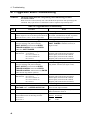
4 - Troubleshooting
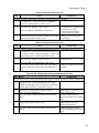
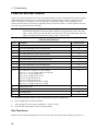
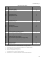
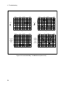
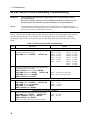
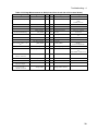
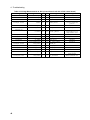
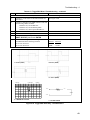
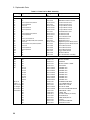
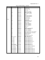
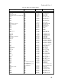
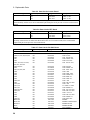
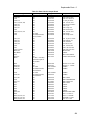
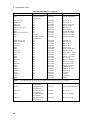
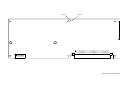
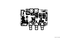
Table 4-9. Voltage Measurements at J821 (viewed from circuit side of A10 control board)
range
signal
pin pin
signal
range
hi
hi
33
34
DDS down
SUB_A0
31
32
SUB_A1
+5 volt bias
29
30
digital common (D10 & X)
RESET
27
28
INPUT_RELAY
SUB_ENB
25
26
PCLR
SENSE_RELAY
23
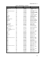
24
SUB_D
+5 volt bias
21
22
OUTPUT_RELAY
normally hi; low true
INHIBIT
19
20
PROT_CLEAR
normally low; hi true
RAIL_INHIBIT
17
18
IPCL_Test
normally hi; low true
normally low
ALC:INT = low;
ALC:EXT = hi
normally low
normally hi
1.5V @ 10 seconds after
power-on
normally hi; low true
normally low
output enabled = 4.95 V
output disabled = 2 mV
pulses hi @ PROT CLEAR
VA_LIMIT
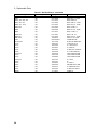
15
16
REG_FAULT
digital common (D10)
13
14
AC_FAULT_MODE
normally hi; low true
SOA_FAULT
11
12
SPARE_IN
normally low; hi true
RAIL_LO_FAULT
9
10
RAIL_LO_WARN
not used
normally hi; low true
DIODE_R_PCLR
7
8
RAIL_HI_FAULT
normally low; hi true
digital common (D10)
5
6
CV_REALTIME
RMS = low; RTIME = hi
CL_RMS
3
4
CL_PEAK
OVP_FAULT
1
2
CV_LEVELING
hi when CC true
normally low; hi true
40
SUB_A2
normally hi
normally low
normally high;
pulsing low true
RMS = hi; RTIME = low