1
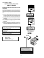
CD-C430H,CP-C430H
SERVICE MANUAL
No. S6739CDC430H/
CD-C430H
CP-C430H
CD-C430H and CP-C430H constitute CD-C430H.
• In the interests of user-safety the set should be restored to its
original condition and only parts identical to those specified be
used.
• SRS technology Licensed from SRS Labe. SRS technology holds
the follwing patents: U.S. Patent No. 4,748,669, U.S. Patent No.
4,841,572 and U.S. Patent No. 4,866,774.
• SRS the SRS Logo ( ) and the SOUND RETRIEVAL SYSTEM
are registered trademarks of SRS Labs, Inc.
• Note for users in UK
Recording and playback of any material may require consent
which SHARP is unable to give. Please refer particularly to the
provisions of Copyright Act 1956, the Dramatic and Musical
Performers Protection Act 1956, the Performers Protection Acts
1963 and 1972 and to any subsequent statutory enactments and
orders.
CONTENTS
Page
SAFETY PRECAUTION FOR SERVICE MANUAL ........................................................................................................... 2
IMPORTANT SERVICE NOTES (FOR UK ONLY) ............................................................................................................ 3
SPECIFICATIONS ............................................................................................................................................................. 3
NAMES OF PARTS ........................................................................................................................................................... 4
OPERATION MANUAL ...................................................................................................................................................... 6
DISASSEMBLY .................................................................................................................................................................. 7
REMOVING AND REINSTALLING THE MAIN PARTS ..................................................................................................... 9
ADJUSTMENT .................................................................................................................................................................. 10
NOTES ON SCHEMATIC DIAGRAM ............................................................................................................................... 12
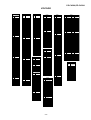
BLOCK DIAGRAM ............................................................................................................................................................ 13
SCHEMATIC DIAGRAM / WIRING SIDE OF P.W.BOARD .............................................................................................. 16
VOLTAGE ........................................................................................................................................................................ 29
WAVEFORMS OF CD CIRCUIT ....................................................................................................................................... 30
TROUBLESHOOTING (CD CHANGER CONTROL / CD SECTION) ............................................................................... 31
FUNCTION TABLE OF IC ................................................................................................................................................ 35
FL DISPLAY ...................................................................................................................................................................... 41
WIRING OF PRIMARILY SUPPLY LEADS (FOR UK ONLY) ......................................................................................... 41
REPLACEMENT PARTS LIST/EXPLODED VIEW
PACKING METHOD (FOR UK ONLY)
SHARP CORPORATION
–1–
CD-C430H,CP-C430H
(For UK)
SAFETY PRECAUTION FOR
SERVICE MANUAL
Precaution to be taken when replacing and servicing the
Laser Pickup.
The AEL (Accessible Emission Level) of Laser Power Output
for this model is specified to be lower than Class I Requirements.
However, the following precautions must be observed during
servicing to protect your eyes against exposure to the Laser
beam.
(1) When the cabinet has been removed, the power is turned
on without a compact disc, and the Pickup is on a position
outer than the lead-in position, the Laser will light for several
seconds to detect a disc. Do not look into the Pickup Lens.
(2) The Laser Power Output of the Pickup inside the unit and
replacement service parts have already been adjusted prior
to shipping.
(3) No adjustment to the Laser Power should be attempted
when replacing or servicing the Pickup.
(4) Under no circumstances look directly into the Pickup Lens
at any time.
(5) CAUTION - Use of controls or adjustments, or performance
of procedures other than those specified herein may result
in hazardous radiation exposure.
(Except for UK)
VARNING-OSYNLIG LASERSTRÅNING NÄR DENNA DEL ÄR
ÖPPNAD. STIRRA EJ IN I STRÅLEN OCH BETRAKTA EJ STRÅLEN
MED OPTISKA INSTRUMENT.
VARO! AVATTAESSA OLET ALTTIINA NÄKYMÄTÖN
LASERSÄTEILYLLE.
ÄLÄ TUIJOTA SÄTEESEEN ÄLÄKÄ KATSO SITÄ OPTISEN
LAITTEEN LÄPI.
VARNING-OSYNLIG LASERSTRÅLNING NÄR DENNA DEL ÄR
ÖPPNAD. STIRRA EJ IN I STRÅLEN OCH BETRAKTA EJ STRÅLEN
GENOM OPTISKT INSTRUMENT.
LASER KLASSE 1
LUOKAN 1 LASERLAITE
KLASS 1 LASERAPPARAT
Laser Diode Properties
Material: GaAIAs
Wavelength: 780 nm
Emission Duration: continuous
Laser Output: max. 0.6 mW
CAUTION-INVISIBLE LASER RADIATION WHEN OPEN. DO NOT STARE INTO
BEAM OR VIEW DIRECTLY WITH OPTICAL INSTRUMENTS.
VARNING-OSYNLIG LASERSTRALNING NAR DENNA DEL AR OPPNAD. STIRRA
EJ IN I STRALEN OCH BETRAKTA EJ STRALEN MED OPTISKA INSTRUMENT.
ADVERSEL-USYNLIG LASERSTRALING VED ABNING. SE IKKE IND I
STRALEN-HELLER IKKE MED OPTISKE INSTRUMENTER.
VARO! AVATTAESSA OLET ALTTIINA NAKYMATON LASERSATEILYLLE.
ALA TUIJOTA SATEESEEN ALAKA KATSO SITA OPTISEN LAITTEEN LAPI.
VARNING-OSYNLIG LASERSTRALNING NAR DENNA DEL AR OPPNAD.
STIRRA EJ IN I STRALEN OCH BETRAKTA EJ STRALEN GENOM OPTISKT
INSTRUMENT.
ADVERSEL-USYNLIG LASERSTRALING NAR DEKSEL APNES. STIRR IKKE
INN I STRALEN ELLER SE DIREKTE MED OPTISKE INSTRUMENTER.
–2–
CD-C430H,CP-C430H
FOR A COMPLETE DESCRIPTION OF THE OPERATION OF THIS UNIT, PLEASE REFER
TO THE OPERATION MANUAL.
IMPORTANT SERVICE NOTES (FOR UK ONLY)
WITHSTANDING
VOLTAGE TESTER
Before returning the unit to the customer after completion of a
repair or adjustment it is necessary for the following withstand
voltage test to be applied to ensure the unit is safe for the
customer to use.
Setting of Withstanding Voltage Tester and set.
Set name
PROBE
+
AC
OUT
-
set value
SHORT-CIRCUIT
AC POWER
SUPPLY CORD
Withstanding Voltage Tester
Test voltage
4,240 VPEAK
3,000 VRMS
Set time
6 secs
Set current(Cutoff current)
4 mA
UNIT
CONNECT THE PROBE
TO GND TERMINAL
OF CHASSIS
OF
PHONO TERMINAL
SCREW
Unit
Judgment
OK: The “GOOD” lamp lights.
NG: The “NG” lamp lights and the buzzor sounds.
CHASSIS
SCREW
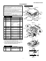
SPECIFICATIONS
CD-C430H
General
Power source:
Power consumption:
Dimensions:
Weight:
Compact disc player section
AC 230 V, 50 Hz
90 W
Width; 270 mm (10-5/8")
Height; 300mm (11-13/16")
Depth; 359.5mm (14-3/16")
5.3 kg (11.7 lbs.)
Type:
Signal readout:
PMPO; 320 W (total)
MPO; 60 W (30 W + 30 W)
(10 % T.H.D.)
RMS; 40 W (20 W + 20 W)
(10 % T.H.D.)
MPO; 60 W (30 W + 30 W) (10 % T.H.D.)
RMS; 40 W (40 W + 40 W) (10 % T.H.D.)
Speakers; 4 ohms
Headphones; 16-50 ohms
(recommended; 32 ohms)
Video/Auxiliary (audio signal);
245 mV/47 kohms
Frequency response:
Signal/noise ratio:
D/A Converter:
Frequency response:
Dynamic range:
Amplifier section
Output power:
(Except for UK)
Output power:
(For UK)
Output terminals:
Input terminals:
Cassette deck section
Wow and flutter:
50 - 14,000 Hz (Normal tape)
55 dB (TAPE 1, playback)
50 dB (TAPE 2, recording/playback)
0.15 % (WRMS)
CP-C430H
Speaker section
Type:
2-way 130 mm (5-1/8") woofer and 50
mm (2") tweeter type
Rated input power:
20 W
Maximum input power: 40 W
Impedance:
4 ohms
Dimensions:
Width; 220 mm (8-11/16")
Height; 300 mm (11-13/16")
Depth; 225 mm (8-13/16")
Weight:
3.0 kg (6.6 lbs.)/each
Tuner section
Frequency range:
3-disc multi-play compact disc player
Non-contact, 3-beam semi-conductor
laser pickup
1-bit D/A converter
20 - 20,000 Hz
90 dB (1 kHz)
FM; 87.5 - 108 MHz
AM; 522 - 1,620 kHz
Specifications for this model are subject to change without prior
notice.
–3–
CD-C430H,CP-C430H
NAMES OF PARTS
CD-C430H
1
Front Panel
1. Disc Tray
2. Disc Number Indicator
3. Timer Indicator
4. Record Indicator
5. Sleep Indicator
6. Extra Bass Indicator: X-BASS
7. Function/CD Track/CD Counter/Frequency/Preset
Channel/Volume/Timer/Sleep Time Indicator
8. Memory Indicator
9. FM Stereo Mode Indicator: ST
10. FM Stereo Indicator:
11. CD Play Indicator:
12. CD Repeat Indicator:
13. SRS Indicator: ( )
14. CD Pause Indicator:
2
1
2
34 5
6
REC
X-BASS
3
SLEEP
11
12
13
7
8 9 10
MEMORY ST
SRS (
)
kHz
MHz
14
15. On/Stand-by Switch
16. Extra Bass/Equalizer Mode Button
17. Volume Up/Down Buttons:
18. 3D Surround Mode Button
19. Clock Button
20. Timer/Sleep Button
21. Function Selector Buttons
22. Memory/Set Button
23. Tuning and Time Up/Down Buttons:
24. Track Down/Review/Preset Down Button:
25. Play/Repeat Button: /
26. Stop Button:
27. Track Up/Cue/Preset Up Button:
28. Disc Skip Button
29. Open/Close Button:
30. Record Pause Button:
31. Headphone Socket
16 17 18
15
19
20
21
22
23
24 25 26 27 28 29 30 31
32
32. (TAPE 1) Cassette Compartment
33. (TAPE 2) Cassette Compartment
–4–
33
CD-C430H,CP-C430H
CD-C430H
Rear Panel
1. Video/Auxiliary (Audio Signal) Input Sockets
2. Speaker Terminals
3. AC Power Lead
4. FM 75 Ohms Aerial Socket
5. AM Loop Aerial Input Socket
1
2
4
5
3
CP-C430H
6
Speaker Section
6. Tweeter
7. Bass Reflex Duct
8. Woofer
9. Speaker Wire
7
7
8
9
Remote Control
1. Remote Control Transmitter LED
1
CD Control section
2. Disc Number Select Buttons
3. Track Down/Review Button:
4. Track Up/Cue Button:
5. Disc Skip Button
6. Play/Repeat Button:
7. Stop Button:
8. Memory Button
9. Clear Button
10. Random Button
11. Pause Button:
5
6
2
3
4
7
8
Tuner control section
12. Preset Up/Down Buttons:
13
14
15
19
21
22
Tape control section
13. (TAPE 1/2) Stop Button:
14. (TAPE 1) Play Button:
15. (TAPE 2) Record Pause Button:
16. (TAPE 2) Play Button:
17. (TAPE 2) Rewind Button:
18. (TAPE 2) Fast Forward Button:
19. Function Selector Buttons
20. Extra Bass/Equalizer Mode Button
21. 3D Surround Mode Button
22. Power Button
23. Volume Up/Down Buttons:
9 10 11
12
16
17
18
20
23
–5–
–6–
9
8
7
6
5
4
3
2
0:00
AM 0:00
TUNING/TIME
(
)
MEMORY/
SET
CLOCK
ON/
STAND-BY
AM 12:00
In this example, the clock is set for the 24-hour
(0:00) system.
SETTING THE CLOCK
Press the ON/STAND-BY switch to enter the stand-by mode.
or
) button to select the time
Press the TUNING/TIME (
or
) button to adjust the
minutes.
Press the button for at least 0.5 seconds to change the time
in 5-minute intervals.
The hour setting will not advance even if minutes advance
from "59" to "00".
Press the MEMORY/SET button.
Press the TUNING/TIME ( or ) button to adjust the hour.
Press the TUNING/TIME button once to advance the time by
1 hour. Press for more than 0.5 seconds to advance continuously.
When the 12-hour display is selected, "AM" will change automatically to "PM".
Press the MEMORY/SET button.
"0:00"
→ The 24-hour display will appear.
(0:00 - 23:59)
"AM 0:00" → The 12-hour display will appear.
(AM 0:00 - PM 11:59)
"AM 12:00" → The 12-hour display will appear.
(AM 12:00 - PM 11:59)
Press the TUNING/TIME (
display mode.
Within 3 seconds, press the MEMORY/SET button.
Press the CLOCK button.
Perform steps 1 - 9 above.
Press and hold down the VOLUME
button, the
button and the ON/STAND-BY switch all at the same time.
Hold them for at least 2 seconds.
(Refer to RESETTING THE MICROCOMPUTER on page 17.)
Press the ON/STAND-BY switch to enter the stand-by mode.
Note:
The operation explained above will erase all data stored in
memory, such as clock and timer settings, tuner and CD presets.
3
1
2
To switch the time display mode:
The time display will appear for about 3 seconds.
Press the CLOCK button.
To see the time display: (When the power is ON)
1 Press the CLOCK button.
2 Within 3 seconds, press the MEMORY/SET button.
3 Perform steps 6 - 9 above.
When the ON/STAND-BY switch is set to ON.
1 Press the MEMORY/SET button.
2 Perform steps 6 - 9 above.
When the ON/STAND-BY switch is set to STAND-BY.
To change the clock time:
Press the MEMORY/SET button.
The clock starts operating from "0" seconds. (Seconds are
not displayed.)
Note:
In the event of a power failure or when the AC power lead
is disconnected, the clock display will go out.
When the AC power supply is restored, the clock display will
flash on and off to indicate the time when the power failure
occurred or when the AC power lead was disconnected.
If this happens, follow the procedure below to change the
clock time.
9
7
8
5
6
1
2
3
4
15
15
1,2
2
RESETTING THE MICROCOMPUTER
0.2 m - 6 m
(8" - 20')
PREPARATION FOR USE
2
1
Press and hold down the VOLUME
button, the
button and the ON/STAND-BY (POWER) switch all at the
same time. Hold them for at least 1 second.
Press the ON/STAND-BY (POWER) switch to enter the standby mode.
Reset the microcomputer under the following conditions:
To erase all of the stored memory contents (clock and timer
settings, tuner and CD presets).
If the display is not correct.
If the operation is not correct.
Periodically clean the transmitter LED on the remote control
and the sensor on the main unit with a soft cloth.
Exposing the sensor on the main unit to strong light may interfere with operation. Change the lighting or the direction of
the unit.
Keep the remote control away from moisture, excessive heat,
shock, and vibrations.
Notes concerning use:
Replace the batteries if control distance decreases or operation becomes erratic.
CD-C430H,CP-C430H
OPERATION MANUAL
CD-C430H,CP-C430H
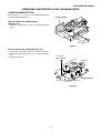
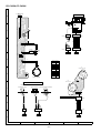
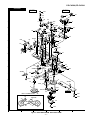
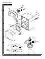
DISASSEMBLY
Caution on Disassembly
Follow the below-mentioned notes when disassembling
the unit and reassembling it, to keep it safe and ensure
excellent performance:
1. Take cassette tape and compact disc out of the unit.
2. Be sure to remove the power supply plug from the wall
outlet before starting to disassemble the unit.
3. Take off nylon bands or wire holders where they need be
removed when disassembling the unit. After servicing
the unit, be sure to rearrange the leads where they were
before disassembling.
4. Take sufficient care on static electricity of integrated
circuits and other circuits when servicing.
CP-C430H
Top Cabinet
( A1 ) x2
ø3 x12mm
Side Panel
(Right)
( A1 ) x2
ø3 x12mm
( B1 ) x1
ø3 x10mm
CD-C430H
PROCEDURE
FIGURE
1
Top Cabinet
1. Screw ..................... (A1) x4
7-1
2
Side Panel
(Left/right)
1. Screw ..................... (B1) x6
7-1
3
CD Player Unit/
CD Tray Cover
1. Turn on the power supply,
open the disc tray, take out
the CD cover, and close.
(Note 1)
2. Hook ....................... (C1) x3
3. Hook ....................... (C2) x2
4. Socket .................... (C3) x4
7-2
1. Screw ..................... (D1) x5
7-2
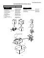
STEP
REMOVAL
( B1 ) x2
ø3 x12mm
( B1 ) x1
ø3 x10mm
Figure 7-1
CD Tray Cover
Push
Back Board
5
Main PWB/
1. Screw ..................... (E1) x12
Display PWB/
2. Socket .................... (E2) x4
Headphone PWB
8-1
6
Front Panel
1. Screw ..................... (F1) x2
2. Hook ....................... (F2) x2
8-1
7
Tape Mechanism 1. Open the cassette holder.
2. Screw...................... (G1) x6
8-2
8
Turntable
1. Screw ..................... (H1) x1
2. Cover ..................... (H2) x1
8-3
9
Disc Tray
1. Screw ..................... (J1) x2
2. Guide ..................... (J2) x2
8-3
10
CD Changer
Mechanism
1. Screw ..................... (K1) x4
8-4
CD Mechanism
1. Screw ..................... (L1) x1
Driver
CD Player Unit
Hook
( C2 ) x1
Push
Driver
( C3 ) x1
( D1 ) x6
ø3 x12mm
( C3 ) x3
Back Board
8-4
Figure 7-2
Note 1:
How to open the changer manually. (Fig. 7-3)
1. Insert the tip of fine screwdriver into the hole of CD player
base, and press down the worm wheel < A > .
2. Then, turn fully the lock lever in the arrow direction through
the hole on the loading chassis bottom in this state.
After that, push forward the CD player base.
<A>
CP-C430H
STEP
1
REMOVAL
Speaker
PROCEDURE
1. Net Frame Ass'y ..... (A1) x1
2. Duct Front Panel .... (A2) x1
3. Screw ...................... (A3) x4
4. Screw ...................... (A4) x4
Hook
( C1) x3
Hook
( C2 ) x1
4
11
Side Panel
(Left)
( B1 ) x2
ø3 x12mm
FIGURE
LOCK
LEVER
7-5
7-6
Figure 7-3
–7–
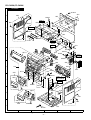
CD-C430H,CP-C430H
Display PWB
( K1 ) x4
ø3 x12mm
Front Panel
( E1 ) x9
ø3 x10mm
( L1 ) x1
ø2.6 x10mm
( E1 ) x1
ø3 x10mm
Shift Lever
( E2 ) x1
( E2 ) x2
CD Changer
Mechanism
( E1 ) x1
ø3 x10mm
Tape
Mechanism
( E2 ) x1
Main PWB
CD Player Base
CD Mechanism
Care when installing the CD changer mechanism.
Install the CD changer mechanism on the CD player base after
the shift lever has been set in the highest position.
Figure 8-4
( E1 ) x1
ø3 x12mm
Figure 8-1
CP-C430H
Front Panel
( G1 ) x6
ø3 x10mm
Front Panel
(A1) x1
Open
SH
AR
P
Cassette
Holder
Power Supply
PWB
( F1 ) x2
ø3 x10mm
Speaker Box
Tape
Mechanism
Screw
driver
Driver should be pried
away from speaker Box.
Figure 8-2
( H1 ) x1
ø3 x10mm
Direction of handle
Figure 8-5
( H2 ) x1
(A2) x2
4 x10mm
Turntable
Speaker Box
Disc Tray
( J1 ) x1
ø3 x10mm
Woofer
( J2 ) x1
( J1 ) x1
ø3 x10mm
CD Player Unit
(A2) x4
4 x32mm
( J2 ) x1
Figure 8-6
Figure 8-3
–8–
CD-C430H,CP-C430H
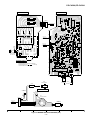
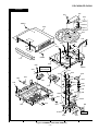
REMOVING AND REINSTALLING THE MAIN PARTS
CD MECHANISM SECTION
Perform steps 1, 2, 3, 10 and 11 of the disassembly method
to remove the CD mechanism.
Loading Motor
How to remove the loading motor
(See Fig. 9-1)
1. Remove the screws (A1) x 2 pcs., to remove the loading
motor.
( A1 ) x2
ø2 x5mm
Figure 9-1
How to remove the pickup (See Fig. 9-2)
1. Remove the screws (C1) x 2 pcs., to remove the shaft (C2).
2. Remove the stop washer (C3) x 1 pc., to remove the gear
(C4).
3. Remove the pickup.
( C1 ) x2
2.6 x6mm
Pickup
( C2 ) x1
( C3 ) x1
CD Mechanism
( C4 ) x1
Figure 9-2
–9–
CD-C430H,CP-C430H
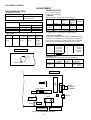
ADJUSTMENT
TUNER SECTION
MECHANISM SECTION
• Driving Force Check
Torque Meter
fL: Low-range frequency
fH: High-renge frequency
• AM IF/RF
Signal generator: 400 Hz, 30%, AM modulated
Specified Value
Play: TW-2412
Tape 1: Over 80 g
Tape 2: Over 80 g
• Torque Check
Torque Meter
Tape 2
30 to 60 g. cm
30 to 60 g.cm
Fast forward: TW-2231
—
60 to 120 g.cm
Rewind: TW-2231
—
60 to 120 g.cm
IF
990 kHz
990 kHz
Band
Coverage
—
522 kHz
(fL): T302 *2
1.1 ± 0.1 V
Tracking
990 kHz
990 kHz
T302
Test Tape
Adjusting
Point
Specified
Value
MTT-111
Volume in
motor.
3,000 ±
30 Hz
Setting/ Instrument
Adjusting Connection
Parts
T351
*1
*1
*1. Input: Antenna, Output: Speaker Terminal
*2. Input: Input is not connected, Output: TP301
• Tape Speed
• Setting the Test Mode
Keeping the TUNING (DOWN) button and MEMORY button
pressed, turn on POWER. Then, the frequency is initially set
in the memory as shown in Table. Call it with the PRESET
button to use it for adjustment and check of tuner circuit.
Instrument
Connection
Speaker
terminal
(Load
resistance:
8 ohms)
Preset No.
FM
Preset No.
1
2
3
4
5
87.50 MHz
108.00 MHz
90.00 MHz
106.00 MHz
98.00 MHz
6
7
8
9
10
TAPE MECHANISM
AM
522 kHz
1,620 kHz
603 kHz
1,404 kHz
990 kHz
11 ~ 40
• FM Mute Level
Signal generator: 1 kHz, 40 kHz dev. FM modulated.
MM 1
Motor
Frequency
Display
Frequency
Volume in motor
98.00 MHz
(25 dBµV)
98.00 MHz
Adjusting
Parts
VR351 *1
Instrument
Connection
Input: So301
Output: Speaker
Terminal
*1. Adjust so that an output signal appears
TUNER PWB
TP301
FE301
Normal
speed
Frequency
Display
Specified Value
Tape 1
Play: TW-2111
Test Stage Frequency
T351 VR351
FM MUTE
AM IF
LEVEL
1
T302
IC303
13
L311
21
R331
TP302
AM BAND
COVERAGE fL
AM TRACKING
fL
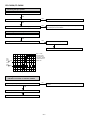
Figure 10-1 ADJUSTMENT POINTS
– 10 –
SO301
ANTENNA
TERMINAL
CNP301
CD-C430H,CP-C430H
TEST MODE
• Setting the test mode
Any one of test mode can be set by pressing several keys as follows.
<REC. PAUSE> + <DISC. SKIP> + <POWER>
TEST: CD operation test
• TEST mode
Function — CD test mode
Setting of TEST mode
Indication of CD TST mode (Fig. 11-1)
IL is not performed.
OPEN/CLOSE operation is manual operation.
The pickup can be moved by using the (
<MEMORY>
LASER ON
<MEMORY>
Tracking on the spot.
SERVO OFF PLAY
<PLAY> key input
) or (
) key.
<STOP>
STOP
<MEMORY>
Tracking on the spot.
SERVO ON PLAY
TOC. IL is performed, and the ordinary PLAY is performed.
If the following key is pressed during PLAY, it is possible
to specify directly any Track No.
<Disc Number 1> key: Track 4
<Disc Number 2> key: Track 9
<Disc Number 3> key: Track 15
Note:
Only in STOP state it is possible to slide the pickup with the (
VOL. --- Last memory
BAL. --- CENTER
R.GEQ. --- FLAT
1
X-BAS --- OFF
) or (
2
Press <STOP> key.
Stop
) key.
3
Canceling method - POWER OFF
Figure 11-1
CD SECTION
Since this CD system incorporates the following automatic adjustment function, when the pickup is replaced, it is not necessary
to readjust it.
Since this CD unit does not need adjustment, the combination of PWB and laser pickup unit is not restricted.
• Automatic adjustment item
1. Focus offset (Fig. 11-2)
2. Tracking offset (Fig. 11-3)
3. E/F balance (tracking error balance) (Fig. 11-4)
4. RF level AGC function (HF level: constant)
5. RF level automatic follow-up of the tracking gain
This automatic adjustment is performed each time a disc is changed. Therefore,
each disc is played back using the optimal settings.
Enlarged
View
10ms
0.50 V
IC1 20 FE
0.1s
0.50 V
IC1 20 FE
FOCUS
OFF-SET
ADJUST
10ms
0.50 V
IC1 7 TE
0.1s
0.50 V
IC1 7 TE
TRACKING
OFF-SET
1 ADJUST
TRACKING
OFF-SET
1 ADJUST
2
2
Figure 11-3
Figure 11-2
TRACKING/
ERROR
BARANCE
1 ADJUST
200 ms
1V/diV
IC 1 15
TO
200 ms
1V/diV
IC 1 7
TE
2
Figure 11-4
– 11 –
CD-C430H,CP-C430H
NOTES ON SCHEMATIC DIAGRAM
• Resistor:
To differentiate the units of resistors, such symbol as K and
M are used: the symbol K means 1000 ohm and the symbol
M means 1000 kohm and the resistor without any symbol is
ohm-type resistor. Besides, the one with “Fusible” is a fuse
type.
• Capacitor:
To indicate the unit of capacitor, a symbol P is used: this
symbol P means micro-micro-farad and the unit of the
capacitor without such a symbol is microfarad. As to
electrolytic capacitor, the expression “capacitance/withstand
voltage” is used.
(CH), (TH), (RH), (UJ): Temperature compensation
(ML): Mylar type
(P.P.): Polypropylene type
• Schematic diagram and Wiring Side of P.W.Board for this
model are subject to change for improvement without prior
notice.
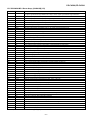
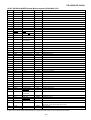
REF. NO
DESCRIPTION
• The indicated voltage in each section is the one measured
by Digital Multimeter between such a section and the chassis with no signal given.
1. In the tuner section,
( ) indicates AM
< > indicates FM stereo
2. In the main section, a tape is being played back.
3. In the deck section, a tape is being played back.
( ) indicates the record state.
4. In the power section, a tape is being played back.
5. In the CD section, the CD is stopped.
• Parts marked with “
”(
) are important for
maintaining the safety of the set. Be sure to replace these
parts with specified ones for maintaining the safety and
performance of the set.
POSITION
REF. NO
SW1
OPEN/CLOSE
ON—OFF
SW713
SW2
MECHA UP
ON—OFF
SW3
DISC NUMBER
SW4
PICKUP IN
SW701
RANDOM/DEMO
SW702
SW703
DESCRIPTION
POSITION
DOWN
ON—OFF
SW714
TUNING UP
ON—OFF
ON—OFF
SW715
TUNING DOWN
ON—OFF
ON—OFF
SW717
POWER
ON—OFF
ON—OFF
SW718
CLOCK
ON—OFF
VOLUME DOWN
ON—OFF
SW719
TIMER/SLEEP
ON—OFF
X-BASS
ON—OFF
SW721
MEMORY/SET
ON—OFF
SW704
VOLUME UP
ON—OFF
SW722
CD
ON—OFF
SW705
OPEN/CLOSE
ON—OFF
SW723
TUNER
ON—OFF
SW706
DISC SKIP
ON—OFF
SW724
TAPE
ON—OFF
SW709
REC./PAUSE
ON—OFF
SW725
AUX
ON—OFF
FOOL PROOF
ON—OFF
SW710
UP
ON—OFF
SWM 3
SW711
STOP
ON—OFF
SWM 4
F.A.S.
ON—OFF
SW712
PLAY
ON—OFF
SWM 5
CAM
ON—OFF
FRONT
VIEW
FRONT
VIEW
E C B
(S) (G) (D)
(1) (2) (3)
B C E
(D)(G) (S)
(3) (2) (1)
2SA1015 GR
2SB561 C
2SC2389 SS
2SC535 C
KRA102 M
KRA109 M
KRC102 M
KRC104 M
KRC107 M
KTA1266 GR
KTA1273 Y
KTC3199 GR
KTC3203 Y
2SD2012 Y
Figure 12 TYPES OF TRANSISTOR
– 12 –
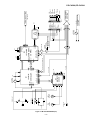
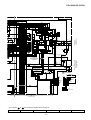
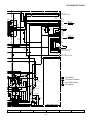
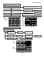
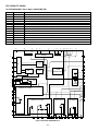
KDV147B
Figure 13 BLOCK DIAGRAM (1/3)
– 13 –
M
M
PICKUP IN
SW4
M1
SPINDLE
MOTOR
M2
SLED
MOTOR
TRACKING COIL
FOCUS COIL
24
25
30
31
12
13
6
7
1
2
3
4
8 9
10 11
IC5
M56748FP
DRIVER
22 32
26
27
28
29
34
35
36
20
30 31 54
5
56
JP– 32
CV+ 40
SLC 43
SL1 44
VCC2
SERVO AMP.
15 16 27 23 29
FIN2
FIN1
E
F
LA9241M
IC1
64
VCC1
62
LD0
Q1
TO
FD
SPO
SP
SLD
~
+5V
SL–
SL+
DRF
20 JP–
PU-IN SW
+B5
SL+. SL–. DRF
CL, DAT, SELIAL CONTROL/CE
51 52 53
44
XOUT
45
XIN
XL1
6
23 36 41 43
+5V
LCHO 37
53 ~ 58
Q91
Q93
26
RES. CQCK. COIN
SQOUT. RWC. WRQ
9
1
+B5
+5V
FROM POWER AMP.
SECTION
VOLTAGE
REGULATOR
+12V(+B3)
SWITCHING
CONT2 25
CONT1 24
IC2
LVSS 38
RVSS 39
LC78623D RCHO 40
9 EFMO SERVO/SIGNAL
10 EFMIN
12 CLV+
CONTROL
~
VOLTAGE
REGULATOR
CL
DAT
CE
VVDD
VDD
LVDD
RVDD
XVDD
PICKUP UNIT
7
Q81
9
8
7
6
5
4
3
2
1
+B5
CNS10
9
8
7
6
5
4
3
2
1
10
SOLM1
M3
LOADING
SW1
OPEN/CLOSE
SW3
DISC NUMBER
SW2
MECHA UP
TO DISPLAY
SECTION
M
FROM POWER AMP.
SECTION
+5V (+B5)
MECHA UP
GND (D)
DISK NO.
OPEN/CLOSE
GND (D)
M–
M+
GND (M)
10 GND (D)
5
6
CNP10
VOLTAGE
REGULATOR
3
IC91
TA7291
MOTOR
CONTROL
( TO IC401 )
TO MAIN SECTION
CD-C430H,CP-C430H
CD-C430H,CP-C430H
+B4
+B6
FM IF
T351
FM IF IN
2
6
4
VCC
3
7
2
MIX
OUT
1
VR351
FM MUTE LEVEL
3
REG
4
21
10
IF OUT
22
AM RF IN
FM OSC
17
7
6
18
16
13
14
15
L-CH
R-CH
12
MUTING
Q35
Q35
+B6
BALUN
VOLTAGE
REGURATER
+B4
AM BAND
COVERAGE
X352
4.5MHz
VT
20
12
1
22
OSC
SWITCHING
FM
Q360
10
16
11
3 4 5 6
IC302
LC72131
PLL
8
9
13
17
21
ST
7
15
CE
DI
CL
DO
T304
AM AMT.
FM IN
AM
TRACKING
AM IN
L311
23
AM OSC OUT
AM OSC IN
24
8
9
FM
DET
MONO/ST
IC303
LA1832
FM IF DET./FM MPX./AM IF
AFC
AM LOOP
ANTENNA
5
L354
FM/AM
CF302
Q301
CF301
5
X351
1
SD
8
AM IF
CF351
FE301
FM FRONT END
STEREO
SO301
ANTENNA
TERMINAL
ST FM
+B4
Q361
MODE
Q206
27 26
IC201
SRS5250S
SRS
CIRCUIT
15
1
+B4
SRS 12V
VCC
Q201
SO401
VIDEO/
AUX.
TAPE
TUNER
CD
FROM CD SECTION
PLAYBACK&RECORD/
PLAYBACK AMP.
IC101
AN7345K
TAPE 1
PB HEAD
L-CH
R-CH
Q106
POP REDUCE 6
REC
L REC 9
R REC 16
AC BIAS
REF
+B4
13
L 4
R 21
L NF 3
R NF 4
P.B
REC
P. B.
L (T2) 2
R (T2) 23
~
TAPE 2
REC/PB
HEAD
L-CH
R-CH
L (T1) 1
R (T1) 24
SWITCHING
Q103
Q121
Q122
MUTING
P. B
L
R
5
20
T1/T2
REC
H/N
7 L REC
R
8 L NF
17 R NF
10 ALC
18
14
T1/T2
12
19
T1/T2
SWITCHING
SWITCHING
Q107
Q108
Q111
Q109
Q110
SWITCHING
BIAS
OCS
ERASE
HEAD
Q128
L104
SWITCHING
BIAS
Q124
Q126
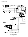
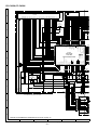
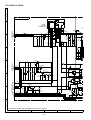
Figure 14 BLOCK DIAGRAM (2/3)
– 14 –
BIAS
CD-C430H,CP-C430H
+B7
+B8
UN-SWITCHED
+B6
FL701
DISPLAY
MONO/ST
1 2
3 ~
14 17 18 21
MEMORY
BACK UP
~
30
31 32 33
M IF
Q701
+B8
14
15
+B7
L-CH
R-CH
FM/AM
12
MUTING
Q353
Q354
TAPE BIAS
TAPE REC
T1/T2
CD DSP WRQ
CD DSP RWC
CD DSP CQCK
CD DSP COIN
CD DSP SQOUT
RESET
CD DSP RES
CD T/T OPEN/CLOSE
13
CD UP DOWN/DISC NO
T2 RRUN PLSE
L-CH INPUT
R-CH INPUT
TO CD SECTION
6
9
7 8
10 11 12 13 14 15 16 17 18 19 20
TO POWER AMP.
SECTION
+B3
PHM1
21 22 23 24
6
~
~
25
27
80
79
77
29
IC701
IX0191AW
SYSTEM CONTROL
MICROCOMPUTER
~
+B6
1
72
TAGE
ATER
B4
71
70
30
34
36
~
37
38
~
39
40
61
13
17
TO CD SECTION
RESET
POWER
CD SL–
CD SL+
CD PUIN
6
CL
DE
DI
DO
DRF
48 47 46 45 44 43 42 41
52 51 50
VDD
TAPE MOTOR
TAPE SOL
TAPE MECHASTOP
T1 RUN PLSE
TAPE FP
DO
VSS
XL701
4.19MHz
35
64
57 56 55
KEY
SW701~706
SW709~715
SW717~725
+B7
+B8
33
65
31
AVDD
AVREF
RESET
Q707
Q708
Q709
ZD701
SYSTEM STOP
+B7
TO CD SECTION
SWM3
FOOL PROOF
21
SWM4
F. A. S
+B7
3
RX701 2
+B9
Q706
1
SOLM2
SOLENOID
ST FM
+B8
+B3
CONSTANT
VOLTAGE
SWM5
CAM
M
Q705
+B3
+B9
MM1
TAPE
MOTOR
PRESET GRAPHIC EQUALIZER
CL
DI
CE
+B4
7
42
5
44
8
41
IC401
LC75394E
AUDIO PROCESSOR
17
32
6
43
9
40
IC801
LA4550
POWER AMP.
49
OUT
58 L
55 R
VOLUME
TO DISPLAY PWB
13
L-IN
9 R-IN
L-OUT
2
5
R-OUT
7 VCC
MUTE
19
30
CD
L
R
21
28
14
GRAPHIC EQUALIZER
13
14
35
56
63
50
26 27
8
12
37
11
38
10
12
NF
3
JK801
HEADPHONES
4
11
+
–
39
SO801
SPEAKER
TERMINAL
X-BASS
VOLTAGE
REGULATOR
+B6
UN-SWITCHED
+5V
Q952
Q953
T961
POWER
TRANSFORMER
D965 ~ D968
ZD951
TO CD SECTION
+B5
+B4
+B3
+5V
+B1
F962
T2.5A L
250V
VOLTAGE
REGULATOR
+12V (ANALOG)
+12V (MOTOR)
TO CD SECTION
Q942
Q941
VOLTAGE
REGULATOR
D961 ~ D964
+B2
Q943
ZD941
ZD972
D971
Q971
VOLTAGE
REGULATOR
VF1
–VP
VF2
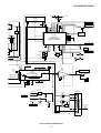
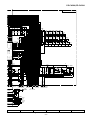
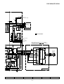
Figure 15 BLOCK DIAGRAM (3/3)
– 15 –
~
L
R
VSS
AVSS
TUNER
LVREF
L
R
45
64
RVREF
R
4
57
VDD
16
33
VREF
TAPE
23 24 25
L
OUT_L
SO401
VIDEO/
AUX.
AC POWER
SUPPLY CORD
D973
F963
T1.6A L
250V
T.F
AC 230 V,50 Hz
CD-C430H,CP-C430H
TO
A
11
4
5
6
7 12
R31
P19 7 - H
TO MOTOR PWB
CNS10
C44
B C E
R96
R95
Q93
R733
27
R730
R728
28
R737
30
32
33
1 2 3
R785
F
C117
C123
B C E
R776
R786
ZD701
D704
D706
D705
R782
R798
R795
SW709
REC/PAUSE
C22
R150
C1
R102
R107 C1
B C E
C102 C107
C108
R108
B C E
Q111
1 2 3
Q110
1 2 3
R110 Q108
F1
T500mA L 250
R763
C809
R811
R767
C843
C844
R835
JK801
R809
R836
HEADPHONES
DISPLAY PWB-A2
HEADPHONS PWB-A3
CNS101
P18 2 - H
TO TAPE MECHANISM
H
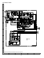
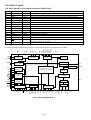
• The numbers 1 to 12 are waveform numbers shown in page 30.
3
4
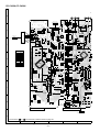
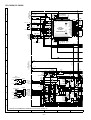
Figure 16 WIRING SIDE OF P.W.BOARD (1/4)
– 16 –
5
6
C813
C812
C811
R777
2
R117
Q107
1
2
3
C453
SW702
VOL-DOWN
G
1
20
C454
R773
SW704
VOL-UP
15
SW705
OP/CL
SW701
RANDOM/DEMO
SW703
X-BASS
C111
C101
SW706
D-SKIP
R701
C709
R101
R764
Q707
B C E
1
C115
R119
R121
D703
C707
C708
Q708
R779
R781
R780
1 2 3
5
C
C121
R123
C855
Q701
Q709
C710
R734
R741
R717
R719
R721
R713
R715
R716
R718
R720
R723
R725
C711
R172
R133
R772
D701
R762
R766
10
C131
C128
C127
L107
C705
R722
C133
R125
SW725
VIDEO/AUX
R761
L701
31
L1
SW710
UP
R768
C147
R137
C141
12
C139
R139
R145
R131
C119
C701
29
C57
R135
C129
R754
C148
B C E
C113
C702
25
26
R732
R794
24
R736
R749
R141
C135
Q121
IC101
C58
D7
D5
R134
PLAY
SW712
R756
SW724
TAPE
80 1
R60
R45
R152
R750
5
23
R58
R47
R46
R109
C46
R738
R751
R757
22
E
R778
R755
10
21
55
XL1
R739
15
70
75
20
20
IC701
60
R88
R87
R86
R792
R746
R745
R729
R747
R748
64
65
19
1
64
50
CNP101
18
R61
R752
R153
17
R57
5
60
R740
TUN
SW723
R35
R56
48 49
C54
C56
C55
PINK
25
24
R82
R38
10
IC2
45
R71
R72
R79
BLACK
PK
55
30
35
C43
STOP
SW711
BK
16
30
32
33
C51
40
R744
35
50
15
C96
R742
R793
WHITE
25
C96
C703
WH(W)
45
17 16
15
20
R753
R3
C3
R3
C53
C59
SW713
DOWN
CD
SW722
XL701
14
R26
R27
R735
C704
13
GRAY
R25
R24
C20
C52
R154
VIOLET
R2
Q81
41 40
12
VL
C1
C16
C81
R700
R703
R705
R706
R709
R731
R726
R727
11
GY
R1
R21
1 2 3
R797
FL701
D
R724
BLUE
R22
SW714
TUN-UP
E C B
R702
BL
ORANGE
R23
C19
R81
R704
10
RED
OR
R708
GREEN
RD(R)
R714
YELLOW
GR
BROWN
R707
YL
3
4
5
6
7
8
9
BR
C11
C17
D91
Q91
R39
C18
R770
R743
R712
COLOR TABLE
10 15
18
R54
R30
SW721
MEMORY/SET
IC91
R789
L700
SW715
TUN-DOWN
C718
1
2
5
R70
R77
R78
R49
R711
R603
C
CNP10
R783
CNSM1
C715
1
2
3
19
20
25
R788
Q705
R758
R760
8
RX701
WH
GY
WH
Q706
E
C
B
30
1
9
8
7
6
5
4
3
2
1
R774
R771
C706
R759
GY
R99
C91
R753
TIMER/SLEEP
SW719
R799
CNPM1
TO TAPE MECHANISM
PWB
WH
GY
WH
E
C
B
BIM1
P18 2 - A
1
D702
1
2
3
4
5
6
7
8
9
10
11
12
R753
R98
R765
RD
R775
B
35
IC5
10 9 8 7 6 5 4 3 2 1
SW718
CLOCK R769
R97
SW717
POWER
D709
D708
C717
36
C95
CD-C430H,CP-C430H
CNP401
1 2 3 4 5 6
R14
IC1
C455
R803
C831
Q942
10 11 12 13 14
B C E
Q941
R406
C973
R972
D972
D971
D973
C851
C847
C849
C845
R844
D963
C852
C848
D961
R843
C943
L831
ZD951
R952
C952
C957
C953
R953
C954
B C E
B
C
E
B C E
LG901
Q952
IC801
C801
R812
R810
C814
R805
CNS901
P19 10 - B
TO POWER PWB
C812
C813
C803
L832
C804
R806
B
C
E
D951
R804
R807
Q953
C830
C829
C802
R808
R945
C825
C823
C810
C811
C955
D965
C454
809
C956
D968
C828
C824
1 2 3 4 5 6 7 8 9
R811
R-CH
C944
D966
C820
C809
C872
C942
R104
R114
453
SO801
SPEAKERS
D967
R106
LG902
R845
L-CH
C871
C850
C846
L104
R166
B C E
R825
F1
T500mA L 250V
C962
C441
Q106
R115
CNP901
6 5 4 3 2 1
C961
D964
C428
C972
C971
R977
D962
R174
Q124
Q126
Q104
C426
C151
R168
C109
E C B
C424
B C E Q128
1 2 3
E C B
C440
C438
C436
C434
R480
C442
Q943
1 2 3
C439
R479
R943
R110 Q108
48 49
C945
Q110
1 2 3
C420
C827
B C E
C101
Q111
7
6
5
4
3
2
1
R112
B C E
C102 C107
C108
R108
C435
C437
C152
R167
R113
C105
R111
Q107
1
2
3
50
C422
Q105
R105
E C B
C116
R120 Q103
R103
E C B
24
C114
R102
R107 C112
C106
R117
R109
C113
R101
CNP101
C111
CNP102
L107
1
C124
C118
R122
L108
R118
1
C115
R119
45
R951
C122
55
C427
C433
R-CH
C408
D401
20
C121
R162 C153
C130
R164
R132
R126
R124
C120
60
40
C218
B C E
Q109
IC101
5
R138
C134
C132
1
64
C418
R158
R160
R146
R140
15
30
35
C941
R949
C947
C146
Q122
R150
R134
R152
10
C131
C128
C127
C145 C142
C140
13
C423
5
C452
L105
R136
R142
C136
C147
R137
C141
12
C139
C133
R476
B C E
C148
C412
R414
R412
C414
C406
C425
10
C444
C405
C68
C135
SO401
VIDEO/AUX
R407
Q971
C976
ZD972
R976
R975
R978
C445
C92
R45
R141
15
20
32
33
C421
C443
C402
R974
E C B
17 16
R418
R419
R420
25
C67
R973
C417
IC401 C419
C401
R60
R47
R46
48 49
C407
C413
D402
R58
L-CH
R408
R411
R415
R416
R478
60
55
50
R413
R475
R405
C409
R477
1
64
C411
C410
R946
C41
R18
C22
45
C42
R57
R73
C69
R75
IC2
R56
C37
D2
C33
R36
C34
C805
10
5
C31
R37
R35
C35
C50
R815
R38
C39
R74
C70
R76
17 16
15
20
C38
R41
C45
C30
R33
C32
R34
R32
C53
5
C40
50
48
Q81
ZD971
45
E C B
1
64 C2
R1
60
55
C974
40
C975
30
35
33
ZD941
R27
R81
C1
5
R422
32
R26
C3
10
C808
C52
25
R421
C20
C451
15
20
C81
C217
R20
C16
R3
R2
C14
R947
C15
D941
R944
R19
R21
R948
R22
R4
C5
C10
C806
C19
R5
R11
C948
D942
R23
C4
R9 C6
R8
R15 R16
R17
C446
R417
C12
C17
R24
C11
C18
R13
C13
R12
R28
3
C456 CNP402
10 9 8 7 6 5 4 3 2 1
R403
R402
R401
R39
D404
D403
CNP1
R6
C9
R7
MAIN PWB-A1
2
C403
R29
18
Q1
R10
C21
C94
C7
9
C404
10 15
CNP2
1 2 3 4 5 6 7 8
5 4 3 2 1
C8
19
20
8
C24
E
C
B
R42
R31
CNP3
6 5 4 3 2 1
C44
25
1
R43
10
C25
7 12
C150
6
P19 9 - C
TO TUNER
PWB
CNP303
P19 9 - C
TO TUNER
PWB
CNP201
P18 5 - C
TO PICKUP
UNIT
CNS1A
P18 5 - C
TO PICKUP
UNIT
CNS2A
P18 6 - H
TO CD MOTOR
PWB
CNS3A
CNS102
P18 3 - H
TO TAPE MECHANISM
ANISM
7
8
9
10
Figure 17 WIRING SIDE OF P.W.BOARD (2/4)
– 17 –
11
12
CD-C430H,CP-C430H
P16 1 - A
TO DISPLAY PWB
CNSM1
PICKUP UNIT
SWM4
F. A. S
1
2
CNS1B 1 2 3 4 5
CNPM2
1 2 3 4 5 6 7 8
CNS2B
1
2
RD
WH
GY
WH
GY
WH
GY
WH
BL
PK
RD
YL
BK
B
CNPM1
12 11 10 9 8 7 6 5 4 3 2 1
R
A
BK
WH
RD
YL
BL
WH
BK
C
1 2 3 4 5
1 2 3 4 5 6 7 8
CNS1A
SOLM1
SOLENOID
CNS2A
SWM5
CAM
SWM3
F. P.
CNP1
P17 8 - A
TO MAIN PWB
FWM1
D
1
WH
2
BK
CNP2
P17 8 - A
TO MAIN PWB
COLOR TABLE
BR
BROWN
RD(R)
RED
OR
ORANGE
YL
YELLOW
GR
GREEN
BL
BLUE
VL
VIOLET
GY
GRAY
WH(W)
WHITE
BK
BLACK
PK
PINK
M1
SPINDLE MOTOR
-
PHM1
4 3
E
1 2
MM1
TAPE MOTOR
+
M2
SLED MOTOR
SW4
PICKUP IN
TAPE MECHANISM PWB-D
+
TAPE 1
TAPE 2
PLAYBACK HEAD(55)
F
ERASE HEAD(56)
RECORD/PLAYBACK HEAD(55)
CNP3A
WH
WH
BK
YL
BK
BL
RD
1 2 3 4 5 6
BK
RD
WH
CD MOTOR PWB-E
GY
BR
GY
1 2 3 4 5 6
CNS3B
1 2 3 4 5 6 7
CNS102
1 2 3
CNS101
RD
BK
WH
BK
WH
RD
BK
WH
YL
BL
RD
WH
GY
WH
GY
WH
G
1 2 3 4 5 6
CNP102
P17 8 - H
TO MAIN PWB
CNP101
P16 6 - H
TO MAIN PWB
CNP3
P17 7 - A
TO MAIN PWB
H
1
2
CNS3A
3
4
Figure 18 WIRING SIDE OF P.W.BOARD (3/4)
– 18 –
5
6
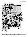
CD-C430H,CP-C430H
TUNER PWB-B
POWER PWB-C3
F963
T1.6A L 250V
R215
1
28
R201
R207
R208
X352
R365
R368
C219
R362
R361
R363
R364
X351
R355
C358
C357
R377
R354
ZD351
CF302
C352
T351
C388
C342
L354
C366
20
R351
24
C350
3
2
1
C363
C364
C325
C361
R358
FM MUTE
LEVEL
C362
L353
C341
R380
C394
C381
R381
C334
Q301
T302
R308
R320
C322
5 6 7 8
R399
R310
C320
L311
C327
D311
FE301
D312
C321
R315
1 2 3 4
C332
R323
L312
C323
CF301
B
C
E
C331
C393
1 2 3
CNP301
1 2
SO301
SW3
DISC NUMBER
FM 75 OHMS
CNS5
2
1
MOTOR PWB-E
SW2
MECHA UP
SW1
OPEN/CLOSE
M3
SELECT MOTOR
CNS10
OR
BR
WH
GY
WH
GY
WH
GY
WH
RD
1
-
SOLENOID
SOLM2
BIM5
P16 4 - B
CNP10
TO MAIN PWB
10
9
8
7
6
5
4
3
2
1
AM LOOP
ANTENNA
2
1
+
6
7
8
9
R205
C365
15
C367
5
C351
R353
C398
C354
C355
10
C399
C396
C386
VR351
L351
IC302
C383
C382
TP301
R318
D352
C375
C397
C390
R360
D364
R387
R376
ZD352
13
14 C385
15
16
17
18
19 R379
20
21
C392
22
R305
R304 R307
When Servicing, pay attention as the area
enclosed by this line (
) is directly
connected with AC main voltage.
R373
R374
Q361
D368
D367
C384
POWER PWB-C
3
2
1
9
8
7
6
5
4
3
2
1
R352
R331
13
1
C387
12 R398
11
10
K951
BF351
R384
C372
C368
C373
12
C370
R395
C374
C371
CF351
C356
1 2 3
R372
AC POWER
SUPPRY CORD
AC 230V,50Hz
R382
R386
Q360
R371
R359
L352
C391
D363
CORE
(265)
B
C
E
R385
CNP303
P17 9 - A
CNP402
TO MAIN PWB
K952
10
9
8
7
6
5
4
3
2
1
R391
R392
R375
R383
R370
CNP201
T.F
Q354
E C B
Q353
E C B
C395
R366
R200
Q201
1
2
3
4
5
6
R204
R356
B C E
R367
C200
C210
R330
R213
C203
C201
R203
Q206
1
2
3
P17 9 - A
CNP401
TO MAIN PWB
R212
5
25
R202
R216
R206
IC201
R234
C202
R218
Q205
TO MAIN PWB
CNP901
P17 11 - G
10
20
C223
D362
1
R210
R217
D361
POWER TRANSFOMER
14
C353 IC303
T961
6
5
4
3
2
1
C220
C240 15
C224
D201
BI901
WH
GY
WH
GY
WH
RD
R228
R233
CNS901
6
R209
F962
T2.5A L 250V
G
D
S
10
Figure 19 WIRING SIDE OF P.W.BOARD (4/4)
– 19 –
11
12
CD-C430H,CP-C430H
A
R1
1K
G
CNP2
TR_
1
TR+
2
FO+
3
FO_
4
GND
5
PD
6
VR
7
LD
8
C33
0.001
+
–
+
1
2
3
4
5
6
7
8
9
10
11
12
13
14
15
37
36
TOFF
35
TGL
34
C31
0.0027
R34
1K
33
29 30 31 32
C53
220P
R24 C18
10K 1/50
C19
47/10
R25
1.2K
SL+
SLD
REF
SLEO
SPO
C16
0.001
38
TES
R27
220K
R26
220K
VREF
39
HFL
C20
0.0033
R16
1.5K
27 28
CV–
SLOF
JP+
R22
6.8K
C14
0.01
SP–
24 25 26
R20
10K
C12
330P
R17
82K
20 21 22 23
SPG
–
R21
56K
FE
18 19
FE–
FA–
17
C30
2.2P
+
SLOF
SLOF
REF
+
–
+–
R41
4.7K
C45
4.7/25
CL
CLK
DEF
CE
DAT
FSS
DRF
VCC2
VR
REF1
S.Q.R
FE1
+–
40
+B
R61
15K
C21
1/50
R10
82K
D2
1SS119
36
35
34
33
32
+5V
31
30
29
28
27
26
25
R31
10K
24
23
22
16
21
17
20
18
19
+B
6
5
4
3
2
1
6
5
4
3
2
1
6
5
4
3
2
1
CNP3
SP+
SP_
SL+
SL_
PU-IN
R54
1K
PUIN
1 2 3
4
H
• NOTES ON SCHEMATIC DIAGRAM can be found on page 12.
1
2
R49
100K
C46
0.022
DRF
6
5
4
3
2
1
CNS3A
CNS3B
CNP3A
M
SLOF
CV+
SL–
SL+
SW4
PICKUP IN
+
–
OR
REF
+
–
REF
R32
56K
41
R35
470
SL–
REF
REF
42
C32
27P
+B
CD MOTOR
PWB-E
M2
SLED
MOTOR
+
–
R23
1.2K
TO
FSC
FOSTA
GEN
SPI
JP
REF
TO
GEN
REF
TD
+
–
REF
JP
GEN
TD–
R33
5.6K
+
JP+
R37
47K
43
JP–
R30
15K
F
+
–
RF
RFSM
R36
47K
R38
33K
R70 1K
R71 1K
R72 1K
1
2
3
4
5
6
7
8
REF
JP
C17
0.47/50
C44
100/10
M
FSTA
C34
0.033
3
4
Figure 20 SCHEMATIC DIAGRAM (1/9)
– 20 –
5
6
SQOUT
COIN
CQCK
1
2
3
4
5
6
7
8
TR_
TR+
FO+
FO_
GND
PD
VR
LD
M1
SPINDLE
MOTOR
GL
THD
44
–
CV+
JPCLO
R15
47K
E
CNS2A
CV–
–+
R29
1K
+B
CNS2B
SLC
+
REF
TH
C13 R12
0.1 15K
PICKUP UNIT
8/12CM
SLOF
RFS–
C11
0.1
C94
0.001
ACTUATOR
TGL1
THDL
REF
R13
33K
+B
FSTA
45
–
REF
+
R19
39K
FO–
LF2
+
–
IC5
M56748FP
FOCUS/TRACKING
SPIN/SLIDE DRIVER
TR–
CL
REF
FD
R39
22K
LASER
SLI
REF
+
16
T–
T+
F+
F–
GND
PD
VR
LD
CE
DRF
SCI
R14
10K
1
2
3
4
5
6
7
8
2FREQ
VCC
TESI
15
D
FO+
+
–
REF
SP
C10 14
180P
+
–
R28
1K
TR+
PHI
TE
REF
13
–
FA
LT0H30P1
R8
12K
DGND
TOSTA
IC1
LA9241M
SERVO
AMP.
–
VCR
REF
TE–
FD–
A
F
C
K
E
A
B
F
+
–
TB
C50
0.1
47
46
FSC
FOSTA
+
5
4
3
2
1
LD GND
R11
3.3K
HFL
+
12
R9
27K
–
+
–
AGND
6
7
C5
0.033
8
R4 C6
2.2K 0.033
9
MON
K
E
B
REF
VCR VCR
REF
VCR
R5
R6 6.8K C7
0.1/50
100
10
R7
C8
C9
1K
0.047 0.068 11
LD
BHI
F
–
C4
0.001
+B
DEF
+
+
E
REF
C
+
–
C15
0.0047
R2
100K
TBC
EFBAL
FE1
–
–
+
R3
10K
5
48
REF
+
3
4
55 54 53 52 51 50 49
+
–
–
+
REF
C3
0.1/50
+
RF
REF
56
JP–
2
FIN1
57
LATOH
FIN2
58
+
1
59
+
1
2
3
4
5
–
–
1
2
3
4
5
61 60
62
LDS
–
1
2
3
4
5
+B
–
F
B
A
E
K
VCC1
64 63
CNP1
LDO
B
CNS1A
R45
1K
R46
1K
R47
1K
R42
560
+B
CNS1B
C35
0.1/50
C24
1/50
3.3V
C38
0.01
–
C25
0.01
C37
220/6.3
C40
0.33/50
4V
+B
C39
0.47/50
–
C1
0.01
+B
C2
47/10
Q1
R43
KTA1266 GR 12
1.5V
5 6
CD-C430H,CP-C430H
MAIN PWB-A1 (1/3)
+B
+B
C56
100P
C57
100P
C54
100P
+B
SFSY
GND
R75
270
C69
220P
CD_L
19
18
35
NC
34
TEST4
33
C43
100/10
C58
0.022
DIGITAL
OUT
24 25 26 27 28 29 30 31
D5
1SS119
EXTERNAL
OUTPUT
SERVO
COMMAND
TES
D7
1SS119
HLF
32
SURR
S_MUTE
IC2
LC78623D
SERVO/SIGNAL
CONTROL
+B
+12V
REGULATOR
+B
R86 1K
R87 1K
R88 1K
Q81
KTC3203 Y
4V
D2
1SS119
+B
+B
C70
220P
V/P
17 18 19 20 21 22 23
C21
1/50
C59
0.022
D_GND
R82
100
L1
0.82µH
+4.3V
C51
0.022
C52
47/10
4.7V
M+12V
5.2V
17
R81
220
+B
GND
16
CD-LD M–
1 2 3 4 5 6 7 8 9
Q91
2SB561 C
+B 11.8V
Q93
R96
KRC102 M 10K
R95
3
2 2.2K
0V
11.8V
11.8V
R98
10K
C91
47/16
R97
2.2K
CD SIGNAL
+B
1 2 3
4
12
13
CNP10
CNS10
1
1 SOL
2
2 GND(M)
3
3 M+
M–
4
4
5
5 GND(D)
6
6 OPEN CLOSE
7
7 DISC NO.
8
8 GND(D)
9
9 MECHA UP
10 GND(D)
10
DISC_NO/UP/DOWN
D_GND
11
CD_OPEN/CLOSE
GND
GND
5 6 7 8 9 10
MOTOR GND
SQOUT
COIN
CQCK
RWC
WRQ
RES
DRF
SL–
SL+
PUIN
M_GND
R70 1K
R71 1K
R72 1K
R77 1K
R78 1K
R79 1K
R99
10K
C95
0.001
15
D+5V
+B
R49
100K
D_GND
F1
T500mA
L 250V
0V
1 0V
C46
0.022
+B
+5V
1
2
MOTOR
PWB-F
BIM5
NC
LOADING
MOTOR DRIVER
IC91
TA7291S
D91
1SS119
CD-LD M+
+5V
P24 2 - A
TO MAIN SECTION
1BIT
DAC
4FS
DIGITAL
FILTER
CLV
DIGITAL
SERVO
20
R76
270
R73
2.7K
36
LVDD
CLV+
CLV_
XL1
FSX
SBCK
RWC
WRQ
COIN
SQOUT
/CQCK
16M
/RES
TEST11
/CS
PW
37
MUTEL
TEST2
C67
10/16
38
LVSS
CD_R
R74
2.7K
39
P26 1 - G,P23 10 - G
TO POWER SECTION,
DISPLAY PWB
C53
220P
40
LCHO
SYNC-DETECT
EFM DEMODULATE
SLICE
LEVEL
CONTROL
EFMIN
TOFF
16
41
C81
220/10
15
EFMO
DOUT
14
VSS
C96
0.022
C68
10/16
42
RVSS
FR
C2F
13
43
RCHO
VVDD
EMPH
12
44
RVDD
CONT5
11
ERROR
COERECT
FLAG
CONTROL
CONT4
10
45
MUTER
ISET
CONT3
R56
1.2K
46
XVDD
CONT2
6
7
8
9
47
XOUT
VVSS
VDD
R34
1K
2KX8
RAM
PDO
VCO
OSC
CLOCK
CONTROL
R57
27K
X-TAL
GENERATOR
CONT1
R32
56K
R35
470
C42
0.047
C31
0.0027
C32
27P
3
R58
680 4
5
48
XIN
PCK
C41
0.047
TA1
JP_
R37
47K
TEST5
4M
TEST1
R18
3.3M
R38
33K
EFLG
SBSY
SUB-CODE
XVSS
FSEQ
33
6K
1
2
µ-COM
INTERFACE
49
DEF1
JP+
R36
47K
64 63 62 61 60 59 58 57 56 55 54 53 52 51 50
TEST3
C50
0.1
C34
0.033
C30
2.2P
R60
1K
C22
0.01
+B
TGL
4.7K
C45
4.7/25
B
C55
100P
R45
1K
R46
1K
R47
1K
1
2
3
4
5
6
+
–
SOLM2
LOCK
M3
SELECT
MOTOR
SW1
OPEN
CLOSE
M
SW2
MECH UP
SW3
DISC NUMBER
CNS5
14
P22 6 - G,P23 8 - G,P23 9 - G
TO DISPLAY PWB
• The numbers 1 to 12 are waveform numbers shown in page 30.
7
8
9
10
Figure 21 SCHEMATIC DIAGRAM (2/9)
– 21 –
11
12
1
2
R771
1.2K
17
29
3
DRF
SL–
SL+
PUIN
0V
R743
10K
+B
24
BIM1
P21 12 - E,P26 1 - G
TO POWER SECTION,CD SECTION
G
H
4
Figure 22 SCHEMATIC DIAGRAM (3/9)
– 22 –
5
0V
1
2
3
4
5
6
7
8
9
10
11
12
8 7 6 5 4 3 2 1
40
• NOTES ON SCHEMATIC DIAGRAM can be found on page 12.
6
41 CD PUIN
42 CD SL+
24
23
22
CD UP/DOWN,DISC NO 21
AVSS 20
CD T.T OPEN/CLOSE 19
R728
R730
R732
R733
R717
R719
R721
R713
R715
R716
R718
R720
R722
R723
R725
1K
1K
10K
10K
1K
1K
1K
1K
1K
1K
1K
1K
1K
1K
1K
R701
100K
R-CH INPUT 24
L-CH INPUT 23
T2 RUN PLSE 22
CD DSP RES 18
RESET 17
CD DSP SQOUT 16
CD DSP COIN 15
CD DSP CQCK 14
CD DSP RWC 13
CD DSP WRQ 12
T1/T2 11
TAPE REC 10
TAPE BIAS
VDD
T0
T1
T2
T3
T4
-24.8V
R734
10K
KEY-3 25
KEY-2 26
SET UP 28
KEY-1 27
NC 32
33
35
34
37
36
38
40
39
C718
0.001
R709
1K
43 CD SL–
44 POWER
45 TUNER SD
46 SYSTEM STOP
47 REMOCON
48 IC
49 P.B. MUTE
50 TAPE SOL
51 TAPE MOTOR
52 VDD
IC701
IX0191AW
SYSTEM
MICROCOMPUTER
R703
10K 1K
67 S9
54 NC
75 S2
R705
10K
R706
R731
10K
2.2K
2.2K
R727
1K
68 S8
53 MIC
71
56 T1 RUN PLSE
76 S1
R700
5.6K
70 S6
69 S7
55 TAPE F.P.
72 S5
57 TAPE MECHA STOP
74 S3
58 DISC1
73 S4
R724
1K
Q705
KTA1273 Y
R702
R704
59 DISC2
77 S0
R603
10K
66 S10
60 DISC3
78 NC
1K
P20
61 S15
B
R714
1K
1K
1K
65 S11
S12
62 S14
1
2
3
4
5
6
7
8
9
1
CNPM1
F
11.7V
+B
Q701
KRC107 M
2
3
R770
10K
11.7V
R707
R708
R712
C711
1/50
T5
7G
8G
1G
2G
3G
4G
9G
4.4V
R711
10K
C710
1/50
P17
P18
P19
P12
P1
P6
VLOAD
P7
P8
P9
P10
P11
P14
80 T7
79 T8
P15
6G
5G
T6
C
P13
63 S13
P16
64
D
POWER
11.7V
+B
+B
CNSM1
11
R758
10
Q706
(1/2W) 2SB561 C
C706
47/16
11.7V
D702
1SS119
R759
10K
–VP
R760
10K
C717
0.022
E
M_12V
D709
1SS119
D708
1SS119
33
32
31
30
29
28
27
26
25
24
23
22
21
20
19
18
17
16
15
14
13
12
11
10
3
4
5
6
7
8
9
P15
P16
P13
P20
P14
P11
P10
P9
P8
P7
P6
5G
P5
P4
6G
7G
P3
P2
8G
P1
P12
P19
P18
P17
1G
2G
3G
4G
9G
F
F
1 F
2 F
C701
0.022
FL701
T2 RUN
+B
GND
MOTOR
30
M-GND
A
MECHA STOP
SOLENOIDO
T1 RUN
FOOL PROOF
28
VF2
VF1
CD-C430H,CP-C430H
C702
220/6.3
-24.8V
R751
100K
R750
100K
R738
R73
R740
R797
AVREF 30
AVDD 29
SRS ON/OFF 31
XT2
VSS
X1 XL7
X2 4.1
CL
CE
DI
DO
DRF
R729
1K
R726
10K
+B
+B
P21 8 - G,P25 11 - D
TO CD SECTION,MAIN SECTION
2 3 1
MOTOR
2
1
PHM1
2
RUN PALS
3
SENSOR
GND
3
4
5 +B
T2 RUNPALS
6
7
8 FOOL PROOF
CNPM
9
T1 RUNPALS
10
SOLENOIDO
11
MECHA STOP
12
TAPE MECHANIS
PWB-D
CD-C430H,CP-C430H
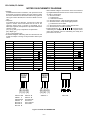
DISPLAY PWB-A2
+B
+B
R750
100K
R756
100K
R749
100
R753
3.3K
R763
R767
R773
R777
R782
1K
1.2K
1.8K
2.2K
3.9K
SW701 SW702 SW703 SW704 SW705
R736
100
R757
100K
R754
3.3K
R751
100K
R737
10K
R734
10K
R741
10K
R738
R739
R740
R797
KEY-3 25
KEY-2 26
KEY-1 27
SET UP 28
8.2K
8.2K
8.2K
1K
1K
1K
1K
VOLUME
DOWN
R764
1K
SW709
X-BASS
/P.G.EQ
VOLUME
UP
OPEN
/CLOSE
SW706
DISK
SKIP
R768
R774
R778
R783
R788
1.2K
1.8K
2.2K
3.9K
5.6K
SW710 SW711 SW712 SW713 SW714 SW715
REC
PAUSE
R752
R755
R744
R742
10K
24
CD UP/DOWN,DISC NO 21
22
23
R728
R730
R732
R733
1K
1K
10K
10K
RANDOM
/SRS
TUNING
UP
R765
R775
R769
1K
1.8K
1.2K
SW717 SW718 SW719
CLOCK
POWER
TIMER
TUNING
DOWN
R789
R792
R793
R794
2.2K
3.9K
5.6K
12K
SW721 SW722 SW723 SW724 SW725
CD
MEMORY
TUNER
/BAND
TAPE
AUX
+B
AVDD 29
AVREF 30
33
34
35
36
39
40
1K
1K
1K
1K
DRF
R729
1K
+B
1
0V
C707
3.3/50
Q708
KTC3199 GR
R779
1K
0.2V
0.2V
2 3 1
4
41 34 33 35
32 31 14 13 10
5 6 7 8 9
12
37 38 36
P21 8 - G,P25 11 - D P27 9 - B
P24 2 - E
TO CD SECTION, TO POWER
TO MAIN
MAIN SECTION
SECTION
SECTION
+
MM1
P21 8 - G
2
TAPE
– 1
TO CD SECTION
MOTOR
4 FWM1
ZD701
MTZJ3.3B
RX701
R799
12
1V
R786
1K
1 2 3
C715
220/6.3
R795
2.2K
D+5V
GND
RES
SQOUT
COIN
CQCK
RWC
WRQ
T1_T2
REC
BIAS
R_CHECK
L_CHECK
DISC_NO/UP/DOWN
CD_OPEN/CLOSE
SD
DO
DI
CE
CL
DRF
SL–
SL+
PUIN
40
8 - G,P25 11 - D
CTION,MAIN SECTION
R785
100
Q709
KTC3199 GR
L701
2.2µH
D704 D706
1SS119 1SS119
+B
R781
10K
R798
150
3
C709
100/6.3
R762
1K
R766
3.3K
D701
1SS119
C705
0.01
+B
+B
R705
10K
R706
R731
10K
C718
0.001
R735
10K
R761
1K
R703
10K 1K
2
D705
1SS119
0V
4.4V
0.2V
Q707
KRC102 M
+B
R780
10K
R726
10K
R772
C708
100K
0.01
R776
82
0.2V
4.4V
41 CD PUIN
42 CD SL+
38
R709
1K
43 CD SL–
44 POWER
37
C703
15P
(CH)
C704
18P
(CH)
D703
1SS119
L-CH INPUT 23
XT2
VSS
X1 XL701
X2 4.19MHz
CL
R745
CE
R746
DI
R747
DO
R748
NC 32
R-CH INPUT 24
T2 RUN PLSE
SRS ON/OFF 31
15
P21 12 - E,P26 1 - G
TO CD SECTION,
POWER SECTION
M
MOTOR
2
PHM1
RUN PALS
SENSOR
GND
3
+B
T2 RUNPALS
1
SWM3
F.P.
FOOL PROOF
CNPM2
T1 RUNPALS
SOLENOIDO
MECHA STOP
1
2
SWM4
F.A.S
SOLM1
SOLENOID
SWM5
CAM
TAPE MECHANISM
PWB-D
7
FWM2
8
9
10
Figure 23 SCHEMATIC DIAGRAM (4/9)
– 23 –
11
12
R403
1K
R406 R407
39K 1.5K
R-CH
VIDEO/
AUX
L-CH
R405 R408 C407
39K 1.5K 390P
SO401
C409
0.047
(ML)
C455
220P
C
R421
1K
TO TUNER GND
C428
0.0039(ML)
C418
0.18(ML)
C420
0.068(ML)
C422
0.18(ML)
C424
0.18(ML)
C426
0.033(ML)
33
34
35
36
37
38
39
40
41
42
43
44
45
46
47
48
C414
100P
C412
22/25
R414
3.3K
C405
R419
0.047(ML) 1K
RF4C2
RF4C3
IC401
LC75394E
AUDIO
PROCESSOR
RFS
RVref
RINVIN2
RTOUT
RVRIN
RTEST
RVROUT
Vref
VDD
LVROUT
LTEST
LVRIN
LTOUT
LINVIN2
LVref
LFS
49
50
51
52
53
54
55
56
57
58
59
60
61
62
63
64
C436
22/16
C438
100P C445
C440 0.022
10/16
C443
22/16
C4
100
C439
10/16
C437
100P
C435
22/16
CE
DI
CL
R3
NC
R2
NC
R1
AVSS
VSS
CE
DI
CL
VSS
L1
NC
L2
NC
L3
2 LF4C2
1 LF4C3
P25 11 - D
33
34
35
C408
390P
B
B
32
31
30
29
28
27
26
25
24
23
22
21
20
19
18
17
C433
0.0027
9
8
7
6
5
C425
4
0.033 C427 3
(ML) 0.0039
2
(ML)
1
A
C406 R420
1K
0.047
(ML) R418
1K
C402 R416
0.047 1K
(ML)
R402
1K
R401
1K
C401
R415
(ML)
0.047
1K
C403
R417
0.047 (ML)
1K
R480
100K
C434
0.0027
C419
0.068(ML)
C421
0.18(ML)
C423
0.18(ML)
TUN_R
TUN_L
R422
1K
R4
RINVIN1
RSEL0
RTIN
RF1C1
RF1C2
RF1C3
RF2C1
RF2C2
RF2C3
RF3C1
47 RF3C2
48 RF3C3
RF4C1
42
43
C410
0.047
(ML)
CD_L
L4
LINVIN1
LSEL0
LTIN
LF1C1
LF1C2
LF1C3
LF2C1
LF2C2
LF2C3
LF3C1
LF3C2
LF3C3
LF4C1
18
R412
22K
A_GND
16
15
14
13
12
11
10
P25 11 - B
19
O
CD_R
C411
22/25
R413
R411 3.3K
22K
C413
100P
C417
0.18(ML)
A
20
C404
0.047
(ML)
P21 12 - C
TO CD SECTION
CD-C430H,CP-C430H
R479
100K
OUT_L
REC_R
GND
D
L105
1.5µH
TAPE_R
R103
2.2K
0.7V
0V
Q103
2SC1845 F
0V
C119
560P
H
• NOTES ON SCHEMATIC DIAGRAM can be found on page 12.
2
3
4
Figure 24 SCHEMATIC DIAGRAM (5/9)
– 24 –
5
17
18
C129
470P
R111
10K
1
R140
560
C132
0.001
R138
6.8K
6
5
R125
5.6K
C127
0.022
4
C123
0.015
C130
470P
R136
3.3K
R132
4.7K
R134
68K
19
20
21
22
23
24
0V
R108
10K
0V
0V
C121
1/50
C113
330P
L107
2.2µH
C115
47/10
C117
0.018
R119
56
C13
0.06
R14
56
C13
22/
R137 C128
3.3/25
6.8K
7
C131
R139
0.001
560
8
0.7V
0V
C111
330P
0.7V
0V
C13
22/
R1
5
R135
3.3K
C105
180P
TAPE2
RECORD/
PLAYBACK HEAD
R117
1K
0V
–
+
Hich=CHRO
+
–
–
112K
+
Hich=T1
+
112K
–
3
0V Q106
2SC1845 F
Q105
2SC1845 F
R105
0V
3.3K
R118
1K
0.7V
C122
1/50
R131
4.7K
L-CH
1
2
3
4
5
6
7
R126
5.6K
R124
3.9K
C116
47/10
L108
2.2µH
R121
100K
R123
3.9K
R-CH
M_GND
ERASE
TAPE2_R2
A_GND
TAPE2_R1
TAPE2_L1
TAPE2_L2
CNP102
Q108
C108
0.001 KTC3199 GR
G
1
2
3
4
5
6
7
0.7V
Q107
KTC3199 GR
ERASE HEAD
Q104
2SC1845 F
C106
180P 0V
CNS102
R104
2.2K
C101
0.001
0V
R120
56 C120
560P
C124
0.015
C118
0.018
R122
100K
C114
330P
C112
330P
2
TAPE1_R 1
A_GND 2
TAPE1_L 3
CNP101
L-CH
R112
10K
R102
1K
R101
1K
R106
3.3K
1
2
3
Q122
KTC3199 G
R133
22K
1
C102
0.001
CNS101
REC
+B
C153
100/16
Q111
KRC104 M
R109
10K
R-CH
R174
150
Q110
KRC104 M
C109
+B
0V
0.047
2
3
R113
3.6V
10K
R114 0V
9.4V
10K
1
1
R115 0V
Q109
3.6V
9.4V 10K
KTA1266 GR
2
3
8.7V
0V
TAPE1
PLAYBACK HEAD
REC
R110
10K
38
F
R476
100K
T1_T2
C107
0.001
37
R107
10K
E
BIAS
0V
P23 9 - G
TO DISPLAY PWB
36
6
C13
0.06
CD-C430H,CP-C430H
R477
1K
OUT_R
MAIN_L
A_GND
MAIN_R
21
22
23
P26 1 - C
TO POWER PWB
R478
1K
C218
2.2/50
R480
100K
C434
0.0027
C436
22/16
C445
0.022
C442
1/50
C443
22/16
C456
100P
C444
100/16
C435
22/16
D402
1SS119
C441
1/50
C439
10/16
C437
100P
C433
0.0027
C217
2.2/50
+B
D403
1SS119
C438
100P
C440
10/16
43
D404
1SS119
42
P28 6 - E
CNP201
TO TUNER PWB
P24 2 - B
A
TUN_R
9 TUN_L
8 A_GND
7 A+12V
6 D_GND
5 SD
4 DO
3 CL
2 DI
1 CE
CNP402
D401
1SS119
C452
2.2/50
OUT_R
IN_R
A-GND
IN_L
OUT_L
A+12V
10
+B
R479
100K
CNP401
1
2
3
4
5
6
+B
+B
OUT_L
REC_R
P28 6 - D
CNP303
TO TUNER PWB
B
GND
33
34
C446
0.022
35
41
40
D_GND
C451
2.2/50
M_GND
A+12V
+B
R475
100K
11
27
P22 6 - G,P23 8 - G
TO DISPLAY PWB
P26 1 - E
TO POWER SECTION
+B
TAPE_L
R476
100K
16
P24 2 - B
REC
C135
0.068
C146
220/10
R164
4.7K
R162
4.7K
+B
R166
47K
IC101
AN7345K
PLAYBACK AND RECORD/
PLAYBACK AMP.
Vcc 13
R158
470
12
11
PLAYBACK SIGNAL
0V
11.6V
C147
0.022
C142
1/50 R146
10K
C145
22/16
R150
10K
15
Nor/
CrO2
RIPPLE 14
16
9
FM SIGNAL
3
1
C139
0.0033
2
Q126
KRC104 M
RECORD SIGNAL
CD SIGNAL
11.7V
11.7V
Q124
2SA1015 GR
0V
R160
150
(1/2W)
Q128
KTC3203 Y
R167
100K
0V
C150
0.0039
(ML)
C151
0.027
(ML)
C129
470P
0V
ALC ALC GND
C141
1/50
R145
10K C148
0.082
R152
1K
C133
22/16
R141
56
R139
560
C128
3.3/25
7
C131
0.001
8
R137
6.8K
0.022
4.7K
R135
3.3K
6
–
+
56K
Hich=CHROME
+
56K
–
10
R142
56
C134
22/16
R172
1K
0V
R140
560
C140
0.0033
C130
470P
C132
0.001
18
17
4.7K
R136
R138 3.3K
6.8K
R134
68K
19
R153 0.6V
10K
C136
0.068
0V
0V
Q121
KTC3199 GR
0V
0V
C152
47/10
L104 R168
12
330µH
Q122
KTC3199 GR
R154
0.7V 10K
0V
MAIN PWB-A1(2/3)
7
8
9
10
Figure 25 SCHEMATIC DIAGRAM (6/9)
– 25 –
11
12
CD-C430H,CP-C430H
A
MAIN PWB-A1(3/3)
–
+
+
–
R811
270
(1/2W)
TO CD GND
(
L8
0
L832
0.29µH
D941
1SS119
11.84V
+B
R825
680
Q942
2SD2012 Y
Q943
KTC3199 GR
+B
D968
1N5402M
D967
1N5402M
D961
RL104A
D962
RL104A
D964
RL104A
C972
100/50
Q952
2SD2012 Y
11
5.7V
C954
10/50
16
28
29
30
R953
10K
D_GND
VF1
–VP
VF2
5.7V
19.1V
Q953
KTC3199 GR
D951
1SS119
C953
0.01
6.32V
C952
47/16
R952
33K
C973
47/50
+B
R951
1.5K
R974
12K
C957
0.022
ZD951
MTZJ6.2C
C976
100/35
C975
47/50
17
+B
C944
4700/25
15
19.1V
ZD972
MTZJ6.2A
R975
220
R976
220
-28.7V
-28V
• NOTES ON SCHEMATIC DIAGRAM can be found on page 12.
2
3
4
Figure 26 SCHEMATIC DIAGRAM (7/9)
– 26 –
5
R
3
-36V
H
1
C974
47/50
ZD971
POWER
5.1V
C95
0.22
(ML)
R947
270
C961
0.047(ML)
R946
100
C943
470/25
ZD941
MTZJ13A
R945
33K
13.1V
D963
RL104A
P22 2 - G,P21 12 - E
TO DISPLAY PWB,CD SECTION
G
C846
0.022
19.3V
12.5V
F
D+5V
M+12V
M_GND
C955
0.22
(ML)
D966
1N5402M
D965
1N5402M
C962
0.047
(ML)
R944
18
R943
18
R973
100
D942
1SS119
R948
22K
C947
10/50
C825
2200/50
12.37V
C942
100/16
24
C848
0.022
C820
+B
19.1V
C941
0.022
11
12.42V
C945
0.022
16
A+12V
D-GND
M-GND
R949
22K
27
+B
19.3V
Q941
2SD2012 Y
11.7V
C948
10/50
E
P25 11 - D
TO MAIN SECTION
+B
C850
0.047
D
C852
0.047
R844
18
R810
4.7
C824
0.022
C823
100/50
R808
180
R809 C813 C811
4.7 0.1(ML) 0.1(ML)
C828
100/50
C808
47/50
C827
100/50
R807
180
C812
0.1
(ML)
C814
0.1
(ML)
C802
0.1
+B
R815
10K
C
C810
2200/25
C801
0.1
C806
1/50
C855
560P
R812
270(1/2W)
C830
47/50
R806
1K
C831
0.001
R805
1K
C45
1/5
C829
47/50
C809
2200/25
C805
1/50
MAIN_R
C803
560P
23
C804
560P
22
R803
33K
21
MAIN_L
R804
33K
P25 11 - A
TO MAIN SECTION
B
14
13
12
11
10
9
8
7
6
5
4
3
2
1
IC801
LA4450
POWER AMP.
6
Q971
KTA1266
CD-C430H,CP-C430H
L_CHECK
R_CHECK
TO CD GND
R836
330
(1/2W)
L831
0.29µH
C844
220P
R835
330
(1/2W)
JK801
HEADPHONES
C843
220P
HEADPHONES
PWB-A3
C872
0.001
C845
0.047
C849
0.022
C847
0.047
C851
0.022
R845
10
C846
0.022
C848
0.022
FM SIGNAL
C871
0.001
C850
0.047
C852
0.047
R843
18
L832
0.29µH
R844
18
R811
270
(1/2W)
R812
270(1/2W)
R809 C813 C811
4.7 0.1(ML) 0.1(ML)
4.7
P23 8 - G
TO DISPLAY PWB
32
C454
1/50
C453
1/50
C855
560P
31
SPEAKER TERMINAL
SO801
+
–
–
+
SP_L-CH
SP_L-CH_GND
SP_R-CH_GND
SP_R-CH
When Servicing, pay attention as the area
enclosed by this line (
) is directly
connected with AC main voltage.
C820
-28.7V
-28V
R976
220
BI901
CNS901
R972
3.3K
-36V
F962
T2.5A
L 250V
CNP901
AC POWER
SUPPLY
CORD(216)
AC 230V 50Hz
CORE
(265)
F963
T1.6A
L 250V
T. F.
R978
2.2
ZD972
MTZJ6.2A
C974
47/50
ZD971
MTZJ3B
R974
12K
R973
100
C976
100/35
C975
47/50
4700/25
C973
47/50
1
2
3
4
5
6
C971
100/50
C972
100/50
R977
2.2
D964
L104A
POWER TRANS FORMER
T961
D973
RL104A
D962
RL104A
1
2
3
4
5
6
1
2
3
4
5
6
C956
0.22
(ML)
C961
0.047(ML)
D961
RL104A
C962
0.047
(ML)
D967
1N5402M
D971
RL104A
D968
5402M
D972
RL104A
D965
5402M
963
04A
C955
0.22
(ML)
D966
1N5402M
Q971
KTA1266 GR
POWER PWB-C
7
8
9
10
Figure 27 SCHEMATIC DIAGRAM (8/9)
– 27 –
11
12
CD-C430H,CP-C430H
R331
470K
C374
0.022
C373
0.022
0.3V
12
C358
1
C355
22P
C357 R355
2.2 3.3K
C352
10
0.3V
0V
R366
10K
Q354
KTC3199GR
R354
3.9K
C370
1
ZD351
MTZJ5.1B
ZD352
MTZJ3.9B
C387
0.022
C388
10
C383
0.022
C385
0.01
R379
2.2K
IO1 IF IN
BO4 IO2
NC
BO3
BO2 AM IN
PD
BO1 FM IN
AIN
DI
CL
DO VDD
CE
2 3 4 5 6 7 8 9
10 11
C386
330P
R395
5.6K
R376
1K
1
2
Q361
KRC107M
C390
470P
SD
D367
1SS199
D368
1SS119
CNP303
C392
0.001
R382
150
C394
47
VSS
R398
1.2K
R360
4.7K
1
2
3
4
5
6
7
8
9
R359
1.8K
C397
220P
SRS_R
IN_R
SRS_GND
OUT_L
SRS_L
A+12V
E
+B
+B
R233
22K
3
4.9V
C220
100/16
SRS_GND
R206
3.9K
R201
33K
IC201
SRS5250S
CR1 16
GND 15
13 CR3
C224
2.2/50
FM SIGNAL
14 CR2
12 CR4 R_OUT 17
CL1 20
Vref 19
L_OUT 18
10 S_IN
11 S_OUT
C240
0.022
(ML)
C223
2.2/50
C6
9
CL2 21
C5
8
CL3 22
C4
CL4 23
C3
7
C_IN 24
C2
5
6
C_OUT 25
R215
4.7K
MODE 26
C1
3
4
PN_IN L_IN 27
PN_OUT
2
R_IN 28
VCC
R202
100K
R204
1.5K
C203
0.0047
R203
22K
R205
47K
C202
0.47/50
R218
1K
AM SIGNAL
SRS CIRCUIT
+B
R217
1K
R216
4.7K
Q205
K246 GR
SRS_L
SRS_R
R200
10K
C210
100/16
C200
100/16
C201
0.022
11.2V
0V
D
4.9V
1
10.6V
11.0V
Q201
KTC3203 Y
R209
10
SRS 1/2
R213
2.2K
Q206
KRC107 M
1
R207
1K
R208
1K
+B
0V
4.0V
G
S
0V
F
2
1
2
3
4
5
6
R228
1K
R234
100
D201
1SS119
CNP401
P25 11 - B
TO MAIN PWB
CNP201
10
TUN_R
TUN_L
A_GND
A_12V
D_GND
SD
DO
CL
DI
CE
C219
0.33/50
R210
1.2K
R212
4.7K
G
TUNER PWB-B
H
• NOTES ON SCHEMATIC DIAGRAM can be found on page 12.
1
2
3
4
Figure 28 SCHEMATIC DIAGRAM (9/9)
– 28 –
5
6
CNP402
P25 11 - C
TO MAIN PWB
D364
1SS119
3
1
1K
1K
0V
AOUT
X352
C382
15P
R384 (CH)
12K
R391
390
D_GND
C384
0.001
L351
100µH
19 18 17 16 15 14 13 12
R392 A_GND
390
R370
R375
R387
22K
C393
1
22 21 20
1K
1K
1K
1K
D
R381 R380
10K 1.5K
R374
R373
R372
R371
D363
1SS119
R386
47K
11.5V
R383
C381 5.6K
12P
(CH)
Q360
KTA1266GR
11.9V
C375
3.3
R368
33K
0V
R377
1K
D362
1SS119
R365
10K
R367
1K
L352
100µH
TP301
TUN_L
D352
1SS119
10 11
0V
0V
(FM/AM) (ST/MONO//STOP)
PHASE
PILOT
L-CH OUT
MPX IN
MPX VCO
R-CH OUT
PHASE
VCC
IF OUT
13
C395
0.022
C396
100
X351
C371 R361
1 4.7K
C398 C356
100 0.001
FM DET
STEREO
C354
0.022
CF351 R353
270
C399 10.7MHz
0.022
9
R352
1K
C353
0.022
BF351
2
T351
AM IF
C350
0.022
3
C368 R356
1K
1
C365
0.022
FM/AM OUT
GND
AM IF IN AM LOW CUT
REG
SD
VSM
AM RF IN
FM AFC
AM OSC IN
AM OSC OUT
FM IF IN
R351
5.6K
AM MIX OUT
1
C351
0.022
2
H:33
N,W,T:56
R310
4.7K
D361
1SS119
3
C325
33P
R304
680
C320
0.022
C322
0.022
R318
470
2
R399
330
C328
0.001
1
0.2V
CF301
C323
0.022
C321
0.022
0.8V
3
7 8
TUN_R
Q353
KTC3199GR
17 16 15 14
3 4 5 6
Q301
2SC380O
9.5V
C391 R385
10K
47
L312
2.2µH
CNP301
1
20 19 18
1 2
R305
6.8K
SO301
ANTENNA
TERMINAL
21
R307
330
CF302
4 3 2 1
R308
33
VT
F OUT
GND
IF OUT
8 7 6 5
R315
82
2
1
ANT
GND
GND
VCC
FE301
24 23 22
IC303
LA1832
R320
10K
AM LOOP
ANTENNA
R330 L354
2.7K
C367
1
T302
AM ANT.
R363
1.8K
R364
1.8K
C372 R362
1 4.7K
TP302
IC302
LC72131
C334
6.8P
(UJ)
L311
BALUN
C
L353
1mH
NC
C366
0.001
C363
0.022
R323
100K
NC
B
D311
1SS119
C361
0.022
R358
8.2K
VR351
10K(B)
C364
22
C341
0.022
FM MUTE
LEVEL
C362
3.3
C332
0.022
X IN X OUT
D312
1SS119
C342
0.022
C327
0.001
C331
0.047
A
CD-C430H,CP-C430H
VOLTAGE
IC2
IC1
PIN
NO.
1
2
3
4
5
6
7
8
9
10
11
12
13
14
15
16
17
18
19
20
21
22
23
24
25
26
27
28
29
30
31
32
33
34
35
36
37
38
39
40
41
42
43
44
45
46
47
48
49
50
51
52
53
54
55
56
57
58
59
60
61
62
63
64
VOLTAGE
2V
2V
2.1V
2.1V
2V
2V
2V
2V
2V
2V
2V
2V
2V
2V
2V
2V
2V
2V
2V
2V
2V
0V
2V
2V
2V
2V
2V
2V
2V
1.8V
1.8V
0V
0V
4V
4V
0V
0V
4V
0V
0V
0.3V
2V
2.1V
2.1V
0V
2V
2V
0V
0V
2V
4V
4V
0V
4V
4V
4V
2.1V
2.1V
0V
0V
2V
3.4V
0V
4V
PIN
NO.
1
2
3
4
5
6
7
8
9
10
11
12
13
14
15
16
17
18
19
20
21
22
23
24
25
26
27
28
29
30
31
32
33
34
35
36
37
38
39
40
41
42
43
44
45
46
47
48
49
50
51
52
53
54
55
56
57
58
59
60
61
62
63
64
VOLTAGE
0V
0V
0V
0V
1.8V
4V
0V
0V
2V
2V
0V
0V
0V
4V
0V
0V
4V
4V
0V
0V
2V
0V
4V
0V
0V
0V
0V
0V
0V
4V
2V
0V
0V
0V
4V
3.8V
1.7V
0V
0V
1.7V
4V
4V
4V
1.8V
1.7V
0V
0V
1.8V
0V
2V
0V
2V
0V
0V
0V
4.4V
4.4V
4.4V
0V
1.6V
2V
0V
0V
0V
IC5
PIN VOLTAGE
NO.
1 2V
2 2V
3 0V
4 2V
5 2V
6 2.2V
7 2.2V
8 0V
9 0V
10 0V
11 0V
12 0V
13 2.2V
14 0V
15 2V
16 0V
17 0V
18 0V
19 0.7V
20 5.2V
21 2V
22 2V
23 2V
24 2V
25 2.2V
26 0V
27 0V
28 0V
29 0V
30 2.2V
31 2.2V
32 2V
33 2V
34 0V
35 0V
36 0V
IC91
PIN VOLTAGE
NO.
1 0V
2 5.1V
3 0.1V
4 0V
5 0V
6 5.1V
7 0V
8 4.2V
9 0V
IC101
PIN VOLTAGE
NO.
1 0V
2 0V
3 0.6V
4 3V
5 0V
6 1.3V
7 0V
8 0.6V
9 3V
10 3V
11 0V
12 0V
13 6V
14 3.7V
15 0V
16 3V
17 0.6V
18 0V
19 0.8V
20 0V
21 3V
22 0.6V
23 0V
24 0V
IC401
IC201
PIN
NO.
1
2
3
4
5
6
7
8
9
10
11
12
13
14
15
16
17
18
19
20
21
22
23
24
25
26
27
28
VOLTAGE
9.8V
4.9V
4.9V
4.9V
4.9V
4.9V
4.9V
9V
4.9V
4.9V
4.9V
4.9V
4.9V
4.9V
0V
4.9V
4.9V
4.9V
4.9V
4.9V
4.9V
4.9V
4.9V
4.9V
4.9V
4.9V
4.9V
4.9V
IC302
PIN
NO.
1
2
3
4
5
6
7
8
9
10
11
12
13
14
15
16
17
18
19
20
21
22
VOLTAGE
2.4V(2.6V)
0V(0V)
0V(0V)
0V(4.3V)
0V(0V)
4.5V(4.4V)
0.2V(3.5V)
4.3V(4V)
10.5V(9.8V)
4V(0V)
4.6V(5.2V)
0V(0V)
4V(0.2V)
0V(0V)
0V(2.5V)
2.3V(0V)
4.3V(5.2V)
0.9V(0.9V)
0.9V(0.9V)
2.4V(1.1V)
0V(0V)
2.5V(2.8 V)
IC303
PIN
NO.
1
2
3
4
5
6
7
8
9
10
11
12
13
14
15
16
17
18
19
20
21
22
23
24
VOLTAGE
2.13V(2.14V)
4.6V(5V)
2.1V(2.1V)
2.1V(2.1V)
0V(0V)
4.5V(4.4V)
4.8V(5.2V)
2.5V(3.5V)
4.6V(5.1V)
0V(0V)
3.4V(2V)
3.4V(1.2V)
3.6V(2.2V) <2V>
1.3V(1.4V)
1.3V(1.4V)
2.1V(2.1V)
2.5V(0V)
2.4V(1.1V)
0V(2V)
1.5V(1.5V)
2.4V(2.1V)
2.4V(2.0V)
4.6V(5.1V)
3V(5.6 V)
– 29 –
PIN
NO.
1
2
3
4
5
6
7
8
9
10
11
12
13
14
15
16
17
18
19
20
21
22
23
24
25
26
27
28
29
30
31
32
33
34
35
36
37
38
39
40
41
42
43
44
45
46
47
48
49
50
51
52
53
54
55
56
57
58
59
60
61
62
63
64
VOLTAGE
5V
5V
5V
5V
5V
5V
5V
5V
5V
5V
5V
5V
5V
5V
5.1V
4.7V
4.7V
0V
4.7V
0V
4.7V
0V
0V
4.4V
0V
0V
0V
4.7V
0V
4.7V
0V
4.7V
4.7V
5.1V
5.1V
5.1V
5.1V
5.1V
5.1V
5.1V
5.1V
5.1V
5.1V
5.1V
5.1V
5.1V
5.1V
5V
5.1V
5.1V
5.1V
5.1V
5.1V
0V
5.1V
5.1V
10.2V
5.1V
0V
5.1V
5.1V
5.1V
5.1V
5.1V
PIN
NO.
1
2
3
4
5
6
7
8
9
10
11
12
13
14
15
16
17
18
19
20
21
22
23
24
25
26
27
28
29
30
31
32
33
34
35
36
37
38
39
40
IC701
VOLTAGE PIN
NO. VOLTAGE
–24.7V
41 0.41V
–24.7V
42 0V
–24.7V
43 0V
–24.7V
44 4.4V
–24.7V
45 0V
–24.7V
46 4.4V
–24.7V
47 4.4V
4.4V
48 0V
0V
49 2.7V
4.4V
50 11.7V
4.4V
51 11.7V
0.24V
52 4.4V
0V
53 4.4V
4.4V
54 4.4V
4.4V
55 0V
0.12V
56 0V
0V
57 4.4V
4.4V
58 0V
0V
59 0V
0V
60 0V
0V
61 –21.2V
3.8V
62 –18V
0V
63 –11.5V
0V
64 –27.8V
4.4V
65 –24.5V
4.4V
66 –14.8V
4.4V
67 –24.5V
0.6V
68 –21.2V
4.4V
69 –27.8V
0V
70 –18V
4.4V
71 –28V
0V
72 –11.5V
2V
73 –24.4V
2V
74 –24.4V
0V
75 14.7V
0V
76 –27.8V
0V
77 –24.4V
4.4V
78 –27.8V
4.4V
79 –27.8V
0V
80 –24.8V
IC801
PIN
NO.
1
2
3
4
5
6
7
8
9
10
11
12
13
14
VOLTAGE
24.7V
14.19V
0V
0V
14.05V
24.8V
31.8V
1.24V
5.3mV
26.7V
0V
2.25V
5.2mV
1.23V
CD-C430H,CP-C430H
WAVEFORMS OF CD CIRCUIT
STOP
FOCUS
1
2
PLAY
SERCH
5ms
0.50 V
IC1 20 F.E
5ms
5.0 V
IC1 54 DRF
0.5ms
10.0 V
JP+
7
0.5ms
10.0 V
JP-
8
0.5ms
0.50 V
JP
9
0.5ms
1.00 V
TE
3
1
3
6
PLAY
CUE
0.5ms
1.00 V
HF
NORMAL DISC
TN0=01
4
0.5ms
5.0 V
HFL
1
5
0.5ms
5.0 V
TES
3
3
0.5ms
1.00 V
HF
10
20ms
1.00 V
SPO
11
20ms
2.00 V
CLV+
2
REVIEW
PLAY
TCD-712 (140mm)
TN0=01
4
5
0.5ms
5.0 V
HFL
1
0.5ms
5.0 V
TES
3
6
50ms
10.0 V
JP+
7
50ms
10.0 V
JP-
8
50ms
0.50 V
JP
9
50ms
1.00 V
TE
6
0.5ms
10.0 V
JP+
7
0.5ms
10.0 V
JP-
8
0.5ms
0.50 V
JP
9
0.5ms
1.00 V
TE
6
50ms
10.0 V
JP+
7
50ms
10.0 V
JP-
8
50ms
0.50 V
JP
9
50ms
1.00 V
TE
2
10
50ms
1.00 V
SPO
11
50ms
2.00 V
CLV+
CUE
PLAY
TCD-712
5s
12 100mV
SLD
1
12
0.5s
100mV
SLD
REVIEW
1
– 30 –
CD-C430H,CP-C430H
TROUBLESHOOTING (CD SECTION)
When the CD does not function
When the CD section does not operate When the objective lens of the optical pickup is dirty,this section may not operate.Clean
the objective lens,and check the playback operation.When this section does not operate even after the above step is taken,check
the following items.
Remove the cabinet and follow the troubleshooting instructions.
"Track skipping and/or no TOC(Table Of Contents) may be caused by build up of dust other foreign matter on the laser pickup lens.
Before attempting any adjustment make certain that the lens is clean. If not, clean it as mentioned below."
Turn the power off.
Gently clean the lens with a lens cleaning tissue and a small amount of isopropyl alcohol.
Do not touch the lens with the bare hand.
• When the turntable fails to stop.
5V
Is from 2.5V
5 V till 2.5V down pulse (approx. 300 ms)
0V
No
input into the IC701 pin 21 when the turntable is rotating?
Check the SWM3 and the wiring from the IC701 pin 21 to the
SWM3.
Yes
Is there following voltage input on the IC701 pin 21 in the
specific state?
When the CD mechanism is moved up: 0V
In other states: 4.3V
No
Check the MECHA UP SW and the wiring from the IC701 pin
21 to the MECHA UP SW.
Yes
Check IC2 pin26 Q91 and Q93 and the periphery.
Yes
IC701 defective.
• When turntable fails to move.
Is there following voltage input on the IC701 pin 21 in the
specific state?
When the CD mechanism is moved up: 0V
In other states: 4.3V
No
Check the MECHA UP SW and the wiring from the IC701 pin
21 to the MECHA UP SW.
Yes
Is L output from the IC2 pin 26 during SEC when the disc skip
switch is pressed?
Check the wiring of IC2 pin 26 and Q93 pin 2.
No
OK
Yes
IC2 defective.
Is 4V output from the Q91 emitter during operation stated
above?
No
Yes
Check turntable motor and turntable mechanism.
– 31 –
Check Q91, Q93 and the periphery.
CD-C430H,CP-C430H
• When the CD tray fails to open or close.
Is there following voltage input in specific state of IC701 pin 19?
Open state: 0V
Close state: 0V
Intermediate state between open state and close state: 4.3V
Check the OPEN CLOSE SW and the wiring from the IC701
pin 19 to the OPEN CLOSE SW.
No
Yes
Is H output to IC2 pin 24 or 25 for 7 seconds when the OPEN/
CLOSE key is pressed?IC91 is defective. Replace it.
Check the wiring of the IC2 pins 24 and 25, IC91 pins 1 and 3.
No
OK
IC2 defective.
Yes
Is 4V output between IC91 pins 3 and 7 during operation
stated above?
Check the periphery of IC91.
No
OK
Yes
IC91 defective.
Check the loading motor (M1) and the loading mechanism.
• The CD function will not work.
The CD operating keys don't work.
Yes
Check the CD, DSP, power supply, and 16.93 MHz clock, and
reset terminal.
Yes
Check the waveform of SCK, SO (DATA) and SI (COMM).
Yes
See if the pick-up is in the pick-up in PICKUP IN SW position.
Focus search is
performed two
times when play
operation is done
without disc.
0.5s
0.50 V
IC1 16 FD
Yes
If the items mentioned above are OK, check the main
microcomputer IC701.
• The CD operating keys work.
0.5s
0.50 V
IC1 7 TE
Check the Focus - HF system.
1
Playback can be performed without a disc.
2
Figure 32
Yes
Does the pick-up move up and down twice?
Yes
Focus search OK
No
Does the output waveform of IC1(16)(FD) match that shown in
Fig. 32?
Check the area around IC5-CNP2.
Yes
No
Check the IC1(50)(CLK) line, 4MHz.
Check the microcomputer data on pins (51)(CL), (52)(DAT)
and (53)CE.
– 32 –
CD-C430H,CP-C430H
• Playback can only be performed when a disc is
loaded.
Is the Focus servo active? (Can you hear it working?)
No
Check the laser diode driver.
Check the area around IC1(16) - (21) (focus servo circuit).
No
If the disc is not turning, the DRF
should not change to "H".
Yes
Yes
Does the DRF signal change from "L" to "H"?
Check the spin system.
Yes
Yes
No
Is HF waveform normal (see the Fig.33-1, 2)?
Check the periphery of
IC1 pins 41 and 42.
Level is abnormal.
Yes
Yes
Check the spin system.
Waveform is unstable.
Check the tracking system.
HF
1.0V/DIV
0.5µsec/DIV(DC)
(When playing
back the disc)
Waveform in case of
normal play-back
0.5s
1.00 V
IC1 16 FD
0.5s
10.0 V
IC2 13 CLV+
2
1
3
0.5s
10.0 V
IC1 54 DRF
4
0.5s
2.00 V
IC1 7 TE
Figure 33-1
Figure 33-2
• Check the tracking system.
Check waveform of IC1 pin 7 (TE).
The waveform shown in
Fig.33-3 appears, and nodisc state appears soon.
Play is possible in
TEST mode.
Yes
Yes
Tracking servo is
inoperative.
Yes
Although IL is possible,
play is impossible.
Data cannot be read.
Yes
Yes
Check the periphery of IC 1
pin 8 to pin 15, and IC 5 to
CNP2.
Normal jump is impeded,
and the program top
cannot be reached.
Check the VCO-PLL system.
5ms
1.00 V
IC1 7 TE
4
5 ms
5.0 V
IC1 54 DRF
3
Figure 33-3
– 33 –
Yes
Check the periphery
of IC 1 pin 14.
CD-C430H,CP-C430H
• Checking the spin system.
Play operation is performed without disc.
Yes
Yes
The turntable rotates a little.
The spin driver circuit is normal.
No
Yes
The turntable fails to rotate or rotates at high speed.
Check the periphery of IC1 pins 23 to 27, pin 39, and pin 40, IC2
pin 12 and pin 13, IC5 to CNP3.
• Checking the VCO-PLL system
Play operation is performed when disc exits.
Yes
Although HF waveform is normal, TOC data cannot be read.
Yes
Check PDO waveform (Fig. 34).
Abnormal
Check the IC1 pins 43 and 44, IC2 pins 3, 5, 7, 10, and 11.
Stop --> Play
As VCO frequency is locked at
4.32 M Hz, voltage
of PDO rises and
stabili- zes.
0.5s
1.00 V
IC2 3 PDO
2
0.5s
1.00 V
IC2 16 FD
3
Figure 34
• Although HF waveform is normal and the time
indication is normal, no sound is emitted.
No
Check IC 2 pin 48 (EFLG).
Yes
Check IC2 pins 37, 40.
Abnomal
Check IC 401 and POWER AMP IC 801.
– 34 –
Usually, the number of pulses of flawless disc is 100 pulses/sec
or less.
CD-C430H,CP-C430H
FUNCTION TABLE OF IC
IC2 VHiLC78623D-1:Servo/Signal Control(LC78623D) (1/2)
Pin No.
Terminal Name Input/Output
1
DEFI
Input
Input terminal of defect detection signal (DEF). (Connected to OV when not used.)
2
TAI
Input
For PLL
3
PDO
4
VVSS
—
5
ISET
Input
6
VVDD
—
Power terminal for integrated VCO.
7
FR
Input
VCO frequency range adjustment.
8
VSS
9
EFMO
Output
10
EFMIN
Input
11
TEST2
Input
12
CLV+
Outout
Output for disk motor control. 3 values can be output with the commands.
13
CLV-
Output
Output for disk motor control. 3 values can be output with the commands.
14
V/P
Output
Monitor output terminal for automatic switch of rough servo/phase control.
"H" for rough servo, and "L" for phase servo.
15
HFL
Intput
Input terminal of track detection signal. Schmit input.
16
TES
Input
Input terminal of tracking error signal. Schmit input.
17
TOFF
Output
Tracking OFF output terminal.
18
TGL
Output
Output terminal for switch of tracking gain "L" increases the gain.
19
JP+
Output
Output for track jump control. 3 values can be output with the commands.
20
JP-
Output
Output for track jump control. 3 values can be output with the commands.
21*
PCK
Output
Clock monitor terminal for EFM data replay. 4,3218MHz as the phase clock.
22*
FSEQ
Output
Output terminal synchronous signal detection. "H" is output when synchronous signal detected
by EFM signal matches synchronous signal internally generated.
23
VDD
24
CONT1
Input/Output
General purpose input/output terminal 1
25
CONT2
Input/Output
General purpose input/output terminal 2
26
CONT3
Input/Output
General purpose input/output terminal 3
27*
CONT4
Input/Output
General purpose input/output terminal 4
28*
CONT5
Input/Output
General purpose input/output terminal 5
29*
EMPH
Output
30*
C2F
Output
C2 flag output terminal.
31*
DOUT
Output
Output terminal of digital OUTPUT. (EIAJ format)
32
TEST3
Input
Input terminal for test. Pull-down resistor is integrated. Surely connected to 0V.
33
TEST4
Input
Input terminal for test. Pull-down resistor is integrated. Surely connected to 0V.
34*
N.C.
35*
MUTEL
36
LVDD
—
37
LCHO
Output
38
LVSS
—
39
RVSS
—
40
RCH0
Output
41
RVDD
—
42*
MUTER
43
XVDD
—
44
XOUT
Output
Ground terminal of 16.9344 MHz quartz oscillator.
45
XIN
Input
Ground terminal of 16.9344 MHz quartz oscillator.
46
XVSS
—
47*
SBSY
Output
Output terminal of synchronous signal of subcode block.
48*
EFLG
Output
Correction monitor terminal of C1, C2, single and double.
Output
—
—
—
Output
Output
Function
Input terminal for test. Pull-down resistor is integrated. Surely connected to 0V.
Output terminal of phase comparison for external VCO control.
Ground terminal for integrated VCO. Surely connected to 0V.
Resistance connection terminal for current adjustment of PDO output.
Ground terminal of digital system. Surely connected to 0V.
For slice level control
EFM signal output terminal.
EFM signal input terminal.
Input terminal for test. Pull-down resistor is integrated. Surely connected to 0V.
Power terminal of digital system.
Controlled with serial data command
from micro computer.
When not used, set it as the input terminal and
open it by connecting to 0V, or set it as the output
terminal and open it.
Difference monitor terminal At "H", deemphasis disk is being replayed.
Terminal not used. Open during operation.
L channel 1 bit DAC
Mute output terminal for L channel.
Power terminal for L channel.
L channel output terminal.
Ground terminal for L channel Surely connected to 0V.
R channel 1 bit DAC
Ground terminal for R channel Surely connected to 0V.
R channel output terminal.
Power terminal for R channel.
Mute output terminal for R channel.
Power terminal for quartz oscillation.
Ground terminal for quartz oscillation. Surely connected to 0V.
In this unit, the terminal with asterisk mark (*) is (open) terminal which is not connected to the outside.
– 35 –
CD-C430H,CP-C430H
IC2 VHiLC78623D-1:Servo/Signal Control(LC78623D) (2/2)
Pin No.
Terminal Name Input/Output
49*
PW
Output
50*
SFSY
Output
51
SBCK
Input
52*
FSX
Output
Output terminal of synchronous signal of 7.35kHz divided from quartz oscillation.
53
WRQ
Output
Output terminal to stand by output of subcode Q.
54
RWC
Input
55
SQOUT
56
COIN
Input
Command input terminal from microcomputer.
57
CQCK
Input
Clock input terminal to fetch command input, or pick up subcode from SQOUT. Schmit input
58
RES
Input
Reset input terminal of LC78622. When turning on power, set it at "L".
59*
TST11
Output
Output
Function
Output terminal of subcodes P, A, R, S, T, U and W.
Output terminal of synchronous signal of subcode frame. It drops when subcode stands by.
Clock input terminal to read subcode. Schmit input (Connected to 0V when not used.)
Input terminal of read/write. Schmit input.
Output terminal of subcode Q.
Output terminal for test. Used in the open state ("L" output as ordinary).
60*
16M
Output
Output terminal of 16.9344Hz.
61
4.2M
Output
Output terminal of 4.2336MHz.
62
TEST5
Input
Input terminal for test Pull-down resistor is integrated. Surely connected to 0V.
63
CS
Input
Chip selection input terminal. Pull-down resistor is integrated.
Connected to 0when not controlled.
64
TEST1
Input
Input terminal for test Pull-down resistor is integrated. Surely connected to 0V.
Note: The same potential must be supplied to the power terminals (VDD, VVDD, LVDD, RVDD, XVDD).
DEFI
EFMIN
FSEQ
Slice level
control
Vss
VDD
TAI
TSTI1
TEST1
TEST2
TEST3
TEST4
TEST5
PCK
FR
I SET
PDO
VVDD
VVss
EFMO
In this unit, the terminal with asterisk mark (*) is (open) terminal which is not connected to the outside.
RAM address
generator
2 K Å~8 b i t
RAM
VCO colck oscillation
clock control
Sync detection
EFM demodulation
Interpolation mute
C2F
Bilingual
Digital OUT
CLV+
CLV-
CLV
Digital servo
Flag processing of C1/C2
error detection and correction
DOUT
Digital
attenuator
V/P
PW
SBCK
SBSY
SFSY
CS
WRQ
SQOUT
Subcode division
QCRC
X4 oversampling
digital filter
(NC)
É COM
Interface
1bitDAC
CQCK
Figure 36 BLOCK DIAGRAM OF IC
– 36 –
LCHO
MUTEL
LVss
LVDD
RCHO
RVss
RVDD
MUTER
EFLG
EMPH
CONT1
CONT2
CONT3
CONT4
CONT5
TGL
JP+
RES
RWC
HFL
TES
TOFF
JP-
L.P.F
XTAL system timing
generator
General-use port
Servo commander
16M
4.2M
XVss
FSX
XIN
XOUT
XVDD
COIN
CD-C430H,CP-C430H
IC1 VHiLA9241M/-1:Servo Amp.,(LA9241M) (1/2)
Pin No.
Function
Port Name
1
FIN2
Connection pin for photodiode of pickup.
RF signal is generated through addition with FIN pin, and FE signal is generated through subtraction.
2
FIN1
Connection pin for photodiode of pickup.
3
E
Connection pin for photodiode of pickup. TE signal is generated through subtraction with F pin.
4
F
Connection pin for photodiode of pickup.
5
TB
Pin for input of DC component of TE signal.
6
TE-
Pin to connect gain setting resistor of TE signal to TE signal.
7
TE
TE signal output pin.
8
TESI
TES (Track error sense) comparator input pin. TE signal is band-passed and input.
9
SCI
Input pin for shock detection.
10
TH
Pin to set time constant of tracking gain.
11*
TA
TA amplifier output pin.
12
TD-
Pin to compose tracking phase compensation constant between TD and VR pins.
13
TD
Pin to set tracking phase compensation.
14
JP
Pin to set amplitude of tracking jump signal (kick pulse).
15
TO
Tracking control signal output pin.
16
FD
Focusing control signal output pin.
17
FD-
Pin to compose focusing phase compensation constant between FD and FA pins.
18
FA
Pin to compose focusing phase compensation constant between FD-/FA-pins.
19
FA-
Pin to compose focusing phase compensation constant between FA and FE pins.
20
FE
Output pin of FE signal.
21
FE-
Pin to connect gain setting resistor of FE signal across TE pin.
22
AGND
GND for analog signal.
23
SP
Single end output for CV+ and CV- pin input.
24
SPI
Spindle amplifier input.
25
SPG
Pin to connect gain setting resistor in the 12cm mode of spindle.
26
SP-
Pin to connect spindle phase compensation constant together with SPD pin.
27
SPD
Spindle control signal output pin.
28
SLEQ
Pin to connect thread phase compensation constant.
29
SLD
Thread control signal output pin.
30
SL-
Input pin of thread feed signal from micro computer.
31
SL+
Input pin of thread feed signal from micro computer.
32
JP-
Input pin of tracking jump signal from DSP.
33
JP+
Input pin of tracking jump signal from DSP.
34
TGL
Input pin of tracking gain control signal from DSP. TGL = Gain low at "H"
35
TOFF
Input pin of tracking off control signal from DSP. TOFF = Off at "H"
36
TES
Output pin of TES signal to DSP.
37
HFL
(HIGH FREQUENCY LEVEL) is used to judge whether main beam is positioned on the bit or on the mirror.
38
SLOF
Thread servo off control input pin.
39
CV-
Pin to input CLV error signal from DSP.
40
CV+
Pin to input CLV error signal from DSP.
41
RFSM
RF output pin.
42
RFS-
Pin to set gain of RF and set 3T compensation constant together with RFSM pin.
43
SLC
(SLICE LEVEL CONTROL) is the output pin to control of the level of the data slice with RF waveform DSP.
44
SLI
Input pin to control the level of data slice with DSP.
45
DGND
GND pin in the digital system.
46
FSC
Output pin for focus search smoothening capacitor.
47
TBC
(Tracking Balance Control) Pin to set EF balance variable range.
48*
NC
No connect.
49
DEF
Defect detection output pin of disk.
50
CLK
Reference clock input pin. 4.23MHz of DSP is input.
In this unit, the terminal with asterisk mark (*) is (open) terminal which is not connected to the outside.
– 37 –
CD-C430H,CP-C430H
IC1 VHiLA9241M/-1:Servo Amp.,(LA9241M) (2/2)
Function
Port Name
Pin No.
51
CL
52
DAT
Micro computer command clock input pin.
Micro computer command data input pin.
53
CE
Micro computer command chip enable input pin.
54
DRF
(DETECT RF) RF level detection output.
55
FSS
(Focus Serch Select) Pin to switch focus search mode. (± search/+ search for reference voltage)
56
VCC2
VCC pin for servo system and digital system.
57
REFI
Pin to connect pass control for reference voltage.
58
VR
Reference voltage output pin.
59
LF2
Pin to set defect detection time constant of disk.
60
PH1
Pin to connect capacitor for peak hold of RF signal.
61
BH1
Pin to connect capacitor for bottom hold of RF signal.
62
LDD
APC circuit output pin.
63
LDS
APC circuit output pin.
64
VCC1
RF system VCC pin.
LDS
63
VCC1
64
LDD
62
BH1
61
PH1
60
APC
FIN2
1
FIN1
2
3
F
4
TB
5
TE-
6
TE
7
TESI
8
SCI
9
VR
58
REFI
57
VCC2
56
FSS DRF CE DAT CL CLK
55 54 53 52 51 50
DEF
49
REF
RF DET
48 NC
47 TBC
VCA
I/V
E
LP2
59
46 FSC
BAL
45 DGND
SLC
µ-COM
VCA
INTER FACE
44 SLI
43 SLC
42 RFS-
TE
41 RFSM
RF AMP
40 CV+
39 CV-
T.SERVO & T.LOGIC
38 SLOF
TH 10
37 HFL
36 TES
TA 11
35 TOFF
34 TGL
TD- 12
F.SERVO & F.LOGIC
SPINDLE SERVO
33 JP+
SLED SERVO
TD 13
JP 14
TO 15
FD 16
17
FD-
18
FA
19
FA-
20
FE
21
22 23
FE- AGND SP
24
SPI
25
SPG
Figure 38 BLOCK DIAGRAM OF IC
– 38 –
26
SP-
27
SPD
28
SLEQ
29
SLD
30 31
SL- SL+
32
JP-
CD-C430H,CP-C430H
IC701 RH-iX0191AWZZ:System Microcomputer (IX0191AW) (1/2)
Pin No.
Port Name
1-7
FIP6-0
8
VDD
Terminal Name
FL DRIVER
Function
Input/Output
Output
—
Segment Output
Connect with BACK UP VDD
9
P27
TAPE BIAS
Output
TAPE BIAS ON: H
10
P26
TAPE REC
Output
TAPE REC. ON:L
11
P25
T1/T2
Output
TAPE2 PLAY:L
12
P24
CD DSP WRQ
13
P23
CD DSP RWC
Output
CD DSP Read write control
14
SCK1
CD DSP CQCK
Output
CD DSP Clock
15
SO1
CD DSP COIN
Output
CD DSP Comand
16
SI1
CD DSP SQOUT
Input
CD DSP Code Q out
17
RESET
RESET
Input
Reset Input: L
18
P74
CD DSP RES
19
P73
CD T/T OPEN/CLOSE
20
AVSS
—
21
ANI7
CD UP/DOWN
CD DISC NO
22
ANI6
23
ANI5
24
25
Input
Outout
Input
—
CD DSP Write request
CD DSP RES interface signal
CD Turntable open close
Connect with GND
Intput
CD mecha up/down CD disc no
T2 RUN PLSE
Input
TAPE2 Run pulse
L-CH CHECK
Input/Output
For TEST mode
ANI4
R-CH CHECK
Input/Output
For TEST mode
ANI3
KEY INPUT 3
Input
Key input 3
26
ANI2
KEY INPUT 2
Input
Key input 2
27
ANI1
KEY INPUT 1
Input
Key input 1
28
ANI0
Initial setting input
Input
Initial setting input
29
AVDD
AVDD
30
AVREF
AVREF
31
P04
SRS
32*
XT2
—
Non connect
33
VSS
—
Connect with GND
34
X1
X1
Input
35
X2
X2
Output
MAIN CLOCK 4.19NHz
36
P37
C2B CL
Output
C2B Bus clock
37
P36
C2B CE
Output
C2B Bus chip enable
C2B Bus comand
2
—
Connect with BACK UP VDD
—
Connect with UNBACK UP VDD
Input
SRS provided/not provided
MAIN CLOCK 4.19MHz
38
P35
C B DI
Output
39
P34
C2B DO
Input
40
P33
CD DRF
Input
Data read fiug from DSP
41
P32
CD PUIN
Input
L: Innermost periphery
42
P31
CD SL+
Output
CD pickup slide motor control
43
P30
CD SL-
Output
CD pickup slide motor control
44
P03
POWER
Output
POWER ON: H
45
P02
TUNER SD
Input
Tuner SD Signal
46
INPT1
SYSTEM STOP
Input
System Stop Signal
47
INPT0
REMOCON
Input
48
IC
INTERNALLY
CONECTED
—
C2B Bus data
Remote Control Code Input
Connect with GND
49*
P72
P.B MUTE
Output
P.B MUTE ON: H
50
P71
TAPE SOL.
Output
TAPE SOL. ON: L
51
P70
TAPE MOTOR
Output
52
VDD
VDD
53
P127
MIC MUTE
54*
P126
—
55
P125
TAPE F.P.
—
Input
Output
Input
TAPE MOTOR ON: L
Connect with BACK UP VDD
MIC MUTE: L
CD STOP, TAPE STOP state: Mute cancel
Non connect
TAPE FOOL PROOF
REC: L
In this unit, the terminal with asterisk mark (*) is (open) terminal which is not connected to the outside.
– 39 –
CD-C430H,CP-C430H
IC701 RH-iX0191AWZZ:System Microcomputer (IX0191AW) (2/2)
Pin No.
Port Name
Terminal Name
Input/Output
56
57
P124
TAPE1 RUN PULSE
Input
TAPE1 Run pluse
P123
TAPE MECHA STOP
Input
Tape mecha up state: L
Function
58*-60*
P122-P120
DISC1-DISC3
Output
Non connect
61-70
FIP25-16
FL DRIVER
Output
Segment output
71
VLOAD
VLOAD
Output
Connect with VPP
72-77
FIP15-FIP10 FL DRIVER
Output
Segment output
78*
P97
—
Output
Non connect
79,80
FIP8,FIP7
FL DRIVER
Output
Segment output
PB CrO2
In this unit, the terminal with asterisk mark (*) is (open) terminal which is not connected to the outside.
FIP21
FIP20
FIP19
FIP18
FIP17
FIP16
V.LOAD
FL DRIVER
SEGMENT
FIP15
FIP14
FIP13
FIP12
FIP11
FL DRIVER
SEGMENT
FIP10
P97
FIP8
FIP7
FL DRIVER
DIGIT
FIP4
80 79 78 77 76 75 74 73 72 71 70 69 68 67 66 65
64 FIP22
63 FIP23
2
62 FIP24
3
FIP3
4
FIP2
5
FIP1
6
FIP0
7
CONNECT WITH VDD
VDD
8
TAPE BIAS
P27
9
TAPE REC
P26
10
T1/T2
P25
11
CD DSP WRQ
P24
12
CD DSP RWC
P23
13
SCK1
14
SO1
15
SI1
16
FIP6
FIP5
CD DSP CQCK
CD DSP COIN
CD DSP SQOUT
RESET INPUT
CD DSP RES
1
61 FIP25
60 P120
µPD78045
DISC 2
57 P123
56 P124
TAPE MECHA STOP
55 P125
54 P126
TAPE F.P.
53 P127
52 VDD
MIC MUTE
51 P70
50 P71
TAPE MOTOR
49 P72
48 IC
RESET 17
P74
18
P33
DRF
C B DO
P34
2
C B DI
P35
2
C B CE
2
C2 B CL
MAIN CLOCK
GND TERMINAL
SRS
CONNECT WITH UN BACK UP VDD
CONNECT WITH VDD
Initial Setting Input
P36
41 P32
24
25 26 27 28 29 30 31 32 33 34 35 36 37 38 39 40
P37
AN14
X2
Rch INPUT
X1
23
Vss
AN15
XT2
22
XT1
AN16
AVREF
T2 RUN PLSE
Lch INPUT
AVDD
21
ANI0
AN17
ANI1
CD UP/DOWN DISC NO
KEY INPUT 1
P.B MUTE
CONNECT WITH GND
CD SL-
20
KEY INPUT 2
TAPE SOL.
43 P30
42 P31
AVSS
ANI2
CONNECT WITH VDD
TUNER SD
CONNECT WITH GND
ANI3
VOL.0 MUTE
45 P02
44 P03
19
KEY INPUT 3
T1 RUN PLSE
REMOCON INPUT
CD T.T OPEN/CLOSE
– 40 –
DISC 1
47 INTP0
46 INTP1
P73
Figure 40 BLOCK DIAGRAM OF IC
DISC 3
59 P121
58 P122
SYSTEM STOP
POWER
CD SL+
CD PUIN
CD-C430H,CP-C430H
Regbase
19
18
Reg5V
20
17
Vcc
Vcc
Vctl3(+)
21
16
N.C
Vctl3(-)
15
Gain2
22
14
Vctl2(-)
Vctl3(out)
PA
13
VM2(-)
23
25
PA
12
VM2(+)
VM3(-)
26
11
24
VM3(+)
27
28
9
10
29
8
GND
VM4(+)
30
VM4(-)
Vctl4(-)
32
10K
31
Gain4
33
Standby
34
35
15K
3.6K
10.8K
OP1
10K
PA
PA
5
6
Vctl(-)
VM1(-)
10K
4
Gain1
GND
3
N.C
7
2
Vrel-out
VM1(+)
1
Vrel-in
10K
OP1
OP1
10K
OP1
TSD
Vcc
10K
10K
OP1
PA
PA
PA
10K
Stand
by
OP1
PA
23K
25K
15K
36
Standby
SS.GND
IC5 VHiM5674FP-1:Focus/Tracking/Spin/Slide Driver (M5674FP)
Figure 41-1 BLOCK DIAGRAM OF IC
FL701 : VVKFiP9EM7R-1
1
2
FL Display
3
REC SLEEP X-BASS
MEMORY ST
WIDE
TA
SRS
kHz DOLBY NR T P
MHz
Figure 41-2 FL DISPLAY
WIRING OF PRIMARILY SUPPLY LEADS (FOR UK ONLY)
If any one of the bands shown in Fig. 41-3 is removed for some
reason, be sure replace it to the original position and same
appearance as before.
Nylon Band 80mm
92LN-BAND 1318A
Core
Power
Transformer
AC Power
Supply Cord
Blue
Brown
Figure 41-3
– 41 –
RDS
CD-C430H,CP-C430H
—MEMO—
– 42 –
CD-C430H,CP-C430H
PARTS GUIDE
MODEL
CD-C430H
CP-C430H
“HOW TO ORDER REPLACEMENT PARTS”
To have your order filled promptly and correctly, please furnish the
following information.
1. MODEL NUMBER
2. REF. No.
3. PART NO.
4. DESCRIPTION
For U.S.A. only
Contact your nearest SHARP Parts Distributor to order.
For location of SHARP Parts Distributor,
Please call Toll-Free;
1-800-BE-SHARP
MARK: SPARE PARTS-DELIVERY SECTION
Explanation of capacitors/resistors parts codes
Capacitors
Resistors
VCC ....................... Ceramic type
VCK ........................ Ceramic type
VCT ........................ Semiconductor type
VC • • MF ............... Cylindrical type (without lead wire)
VC • • MN ............... Cylindrical type (without lead wire)
VC • • TV ................ Square type (without lead wire)
VC • • TQ ............... Square type (without lead wire)
VC • • CY ............... Square type (without lead wire)
VC • • CZ ............... Square type (without lead wire)
VC • • • • • • • • • J .. The 13th character represents capacity difference.
("J" ±5%, "K" ±10%, "M" ±20%, "N" ±30%,
"C" ±0.25 pF, "D" ±0.5 pF, "Z" +80-20%.)
VRD ....................... Carbon-film type
VRS ........................ Carbon-film type
VRN ....................... Metal-film type
VR • • MF ............... Cylindrical type (without lead wire)
VR • • MN ............... Cylindrical type (without lead wire)
VR • • TV ................ Square type (without lead wire)
VR • • TQ ............... Square type (without lead wire)
VR • • CY ............... Square type (without lead wire)
VR • • CZ ............... Square type (without lead wire)
VR • • • • • • • • • J .. The 13th character represents error.
("J" ±5%, "F" ±1%, "D" ±0.5%.)
If there are no indications for the electrolytic capacitors, error is ±20%.
If there are no indications for other parts, the resistors are ±5%
carbon-film type.
NOTE:
Parts marked with “
” are important for maintaining the safety of the set.
Be sure to replace parts with specified ones for maintaining the safety and performance of the set.
– 43 –
CD-C430H,CP-C430H
NO.
PRICE
RANK
PART CODE
DESCRIPTION
NO.
CF301,302
CF351
CD-C430H
INTEGRATED CIRCUITS
VHILA9241M/-1
VHILC78623D-1
VHIM56748FP-1
J
J
J
IC91
IC101
IC201
IC302
IC303
VHITA7291S/-1
VHIAN7345K/-1
VHISRS5250S-1
VHILC72131/-1
VHILA1832//-1
J
J
J
J
J
IC401
IC701
VHILC75394E-1
RH-IX0191AWZZ
J
J
IC801
VHILA4450//-1
J
AS Servo Amp.,LA9241M
AY Servo/Signal Control,LC78623D
AR Focus/Tracking/Spin/Slide
Driver,M56748FP
AH Loading Motor Driver, TA7291S
AM Record/Playback Amp.,AN7345K
BL SRS,SRS5250S
AP PLL (Tuner),LC72131
AR FM IF Det./FM Mpx./ AM IF,
LA1832
AX Audio Processor,LC75394E
AZ System Microcomputer,
IX0191AW
AH Power Amp.,LA4450
VSKTA1266GR-1
VSKTC3203Y/-1
VS2SB561-C/-1
VSKRC102M//-1
VS2SC1845F/-1
VSKTC3199GR-1
VSKTA1266GR-1
VSKRC104M//-1
VSKTC3199GR-1
VS2SA1015GR-1
VSKRC104M//-1
VSKTC3203Y/-1
VSKTC3203Y/-1
VS2SK246GR/-1
VSKRC107M//-1
VS2SC380-O/-1
VSKTC3199GR-1
VSKTA1266GR-1
VSKRC107M//-1
VSKRC107M//-1
VSKTA1273Y/-1
VS2SB561-C/-1
VSKRC102M//-1
VSKTC3199GR-1
VS2SD2012Y/-1
VSKTC3199GR-1
VS2SD2012Y/-1
VSKTC3199GR-1
VSKTA1266GR-1
J
J
J
J
J
J
J
J
J
J
J
J
J
J
J
J
J
J
J
J
J
J
J
J
J
J
J
J
J
AB
AC
AC
AC
AC
AB
AB
AC
AB
AB
AC
AC
AC
AB
AC
AC
AB
AB
AC
AC
AE
AC
AC
AB
AF
AB
AF
AB
AB
Silicon,PNP,KTA1266 GR
Silicon,NPN,KTC3203 Y
Silicon,PNP,2SB561 C
Digital,NPN,KRC102 M
Silicon,NPN,2SC1845 F
Silicon,NPN,KTC3199 GR
Silicon,PNP,KTA1266 GR
Digital,NPN,KRC104 M
Silicon,NPN,KTC3199 GR
Silicon,PNP,2SA1015 GR
Digital,NPN,KRC104 M
Silicon,NPN,KTC3203 Y
Silicon,NPN,KTC3203 Y
FET,2SK246 GR
Digital,NPN,KRC107 M
Silicon,NPN,2SC380 O
Silicon,NPN,KTC3199 GR
Silicon,PNP,KTA1266 GR
Digital,NPN,KRC107 M
Digital,NPN,KRC107 M
Silicon,PNP,KTA1273 Y
Silicon,PNP,2SB561 C
Digital,NPN,KRC102 M
Silicon,NPN,KTC3199 GR
Silicon,NPN,2SD2012 Y
Silicon,NPN,KTC3199 GR
Silicon,NPN,2SD2012 Y
Silicon,NPN,KTC3199 GR
Silicon,PNP,KTA1266 GR
VHD1SS119//-1
VHD1SS119//-1
VHD1SS119//-1
VHD1SS119//-1
VHD1SS119//-1
VHD1SS119//-1
VHD1SS119//-1
VHD1SS119//-1
VHD1SS119//-1
VHD1SS119//-1
VHD1SS119//-1
VHD1SS119//-1
VHD1SS119//-1
VHD1SS119//-1
VHDRL104A//-1
VHD1N5402M/-1
VHDRL104A//-1
VHPI31535CD-1
VHEMTZJ5R1B-1
VHEMTZJ3R9B-1
VHEMTZJ3R3B-1
VHEMTZJ130A-1
VHEMTZJ6R2C-1
VHEMTZJ300B-1
VHEMTZJ6R2A-1
J
J
J
J
J
J
J
J
J
J
J
J
J
J
J
J
J
J
J
J
J
J
J
J
J
AA
AA
AA
AA
AA
AA
AA
AA
AA
AA
AA
AA
AA
AA
AB
AE
AB
AG
AC
AC
AA
AC
AC
AB
AA
Silicon,1SS119
Silicon,1SS119
Silicon,1SS119
Silicon,1SS119
Silicon,1SS119
Silicon,1SS119
Silicon,1SS119
Silicon,1SS119
Silicon,1SS119
Silicon,1SS119
Silicon,1SS119
Silicon,1SS119
Silicon,1SS119
Silicon,1SS119
Silicon,RL104A
Silicon,1N5402M
Silicon,RL104A
Phote Interrupter
Zener,5.1V,MTZJ5.1B
Zener,3.9V,MTZJ3.9B
Zener,3.3V,MTZJ3.3B
Zener,13V,MTZJ13A
Zener,6.2V,MTZJ6.2C
Zener,3V,MTZJ3B
Zener,6.2V,MTZJ6.2A
RFILA0009AWZZ
J
AE AM IF
TRANSISTORS
DIODES
D2
D5
D7
D91
D201
D311,312
D352
D361~364
D367,368
D401~404
D701~706
D708,709
D941,942
D951
D961~964
D965~968
D971~973
PHM1
ZD351
ZD352
ZD701
ZD941
ZD951
ZD971
ZD972
FILTERS
BF351
RFILF0072AFZZ
RFILF0003AWZZ
J
J
DESCRIPTION
AG FM IF
AK FM IF
TRANSFORMERS
IC1
IC2
IC5
Q1
Q81
Q91
Q93
Q103~106
Q107,108
Q109
Q110,111
Q121,122
Q124
Q126
Q128
Q201
Q205
Q206
Q301
Q353,354
Q360
Q361
Q701
Q705
Q706
Q707
Q708,709
Q941,942
Q943
Q952
Q953
Q971
PRICE
RANK
PARTS CODE
!
T302
T351
T961
RCILZ0014AWZZ
J
RCILI0011AWZZ
J
RTRNP0121AWZZ J
AL AM Antenna
AD AM IF
BD Power
VP-XHR82K0000
VP-MK331K0000
VP-DH1R5K0000
VP-XH2R2K0000
RBLN-0001AWZZ
VP-DH2R2K0000
VP-DH101K0000
VP-DH102K0000
RCILL0001AWZZ
VP-XH2R2K0000
VP-DH2R2K0000
RCILZ0137AFZZ
J
J
J
J
J
J
J
J
J
J
J
J
AC
AB
AC
AB
AD
AB
AB
AB
AG
AB
AB
AA
J
AB 10 kohm (B),Semi-VR
[FM Mute Level]
J
J
J
J
AD
AH
AF
AH
Crystal,456 kHz
Crystal,4.5 MHz
Ceramic,16.93 MHz
Crystal,4.19 MHz
J
J
J
J
J
J
J
J
J
J
J
J
J
J
J
J
J
J
J
J
J
J
J
J
J
J
J
J
J
J
J
J
J
J
J
J
J
J
J
J
J
J
J
J
AA
AB
AB
AA
AA
AB
AA
AA
AA
AB
AA
AB
AA
AA
AA
AA
AB
AB
AA
AB
AA
AB
AA
AB
AA
AA
AA
AA
AB
AB
AA
AA
AA
AA
AB
AB
AA
AB
AA
AB
AA
AA
AA
AA
0.01 µF,16V
47 µF,10V,Electrolytic
0.1 µF,50V,Electrolytic
0.001 µF,50V
0.033 µF,16V
0.1 µF,50V,Electrolytic
0.068 µF,16V
0.047 µF,16V
180 pF,50V
0.1 µF,16V
330 pF,50V
0.1 µF,16V
0.01 µF,16V
0.0047 µF,16V
0.001 µF,50V
0.47 µF,50V,Electrolytic
1 µF,50V,Electrolytic
47 µF,10V,Electrolytic
0.0033 µF,16V
1 µF,50V,Electrolytic
0.01 µF,16V
1 µF,50V,Electrolytic
0.01 µF,16V
2.2 pF,50V
0.0027 µF,16V
27 pF,50V
0.001 µF,50V
0.033 µF,16V
0.1 µF,50V,Electrolytic
220 µF,6.3V,Electrolytic
0.01 µF,16V
0.47 µF,50V,Electrolytic
0.33 µF,50V,Electrolytic
0.047 µF,16V
100 µF,10V,Electrolytic
4.7 µF,25V,Electrolytic
0.022 µF,6.3V
0.1 µF,16V
0.022 µF,25V
47 µF,10V,Electrolytic
220 pF,50V
100 pF,50V
0.022 µF,25V
0.022 µF,25V
COILS
L1
L104
L105
L107,108
L311
L312
L351,352
L353
L354
L700
L701
L831,832
0.82 µH,Choke
330 µH,Choke
1.5 µH
2.2 µH,Choke
Balun
2.2 mmH,Peaking
100 µH,Choke
1 mH,Choke
3.9 mH
2.2 µH,Choke
2.2 mmH,Peaking
0.29 µH
VARIABLE RESISTOR
VR351
RVR-M0999AFZZ
VIBRATORS
X351
X352
XL1
XL701
RCRM-0075AFZZ
RCRSP0002AWZZ
RCRM-0008AWZZ
RCRSP0003AWZZ
CAPACITORS
C1
C2
C3
C4
C5,6
C7
C8
C9
C10
C11
C12
C13
C14
C15
C16
C17
C18
C19
C20
C21
C22
C24
C25
C30
C31
C32
C33
C34
C35
C37
C38
C39
C40
C41,42
C43,44
C45
C46
C50
C51
C52
C53
C54~57
C58
C59
–1–
VCTYMN1CY103N
RC-GZA476AF1A
RC-GZA104AF1H
VCKYMN1HB102K
VCTYPA1CX333K
RC-GZA104AF1H
VCTYPA1CX683K
VCTYPA1CX473K
VCKYMN1HB181K
VCTYPA1CX104K
VCKYMN1HB331K
VCTYPA1CX104K
VCTYMN1CY103K
VCTYMN1CX472K
VCKYMN1HB102K
RC-GZA474AF1H
RC-GZA105AF1H
RC-GZA476AF1A
VCTYMN1CX332K
RC-GZA105AF1H
VCTYMN1CY103N
RC-GZA105AF1H
VCTYMN1CY103N
VCCSMN1HL2R2C
VCTYMN1CX272K
VCCSMN1HL270J
VCKYMN1HB102K
VCTYPA1CX333K
RC-GZA104AF1H
RC-GZA227AF0J
VCTYMN1CY103K
RC-GZA474AF1H
RC-GZA334AF1H
VCTYPA1CX473K
RC-GZA107AF1A
RC-GZA475AF1E
VCTYMN0JY223N
VCTYPA1CX104K
VCTYMN1EF223Z
RC-GZA476AF1A
VCKYBT1HB221K
VCKYMN1HB101K
VCTYMN1EF223Z
VCTYBT1EF223Z
CD-C430H,CP-C430H
NO.
C67,68
C69,70
C81
C91
C92
C94,95
C96
C101,102
C105,106
C107,108
C109
C111~114
C115,116
C117,118
C119,120
C121,122
C123,124
C127
C128
C129,130
C131,132
C133,134
C135,136
C139,140
C141,142
C145
C146
C147
C148
C150
C151
C152
C153
C200
C201
C202
C203
C210
C217,218
C219
C220
C223,224
C240
C320~323
C325
C327
C331
C332
C334
C341,342
C350,351
C352
C353,354
C355
C356
C357
C358
C361
C362
C363
C364
C365
C366
C367,368
C370~372
C373,374
C375
C381
C382
C383
C384
C385
C386
C387
C388
C390
C391
C392
C393
C394
C395
C396
PRICE
RANK
PART CODE
RC-GZA106AF1C
VCKYMN1HB221K
RC-GZA227AF1A
RC-GZA476AF1C
VCTYMN1EF223Z
VCKYMN1HB102K
VCKYBT1HB102K
VCKYMN1HB102K
VCKYMN1HB181K
VCKYMN1HB102K
VCKZPA1HF473Z
VCKYMN1HB331K
RC-GZA476AF1A
VCTYMN0JY183M
VCKYMN1HB561K
RC-GZA105AF1H
VCTYMN0JY153M
VCTYMN1EF223Z
RC-GZA335AF1E
VCKYMN1HB471K
VCKYMN1HB102K
RC-GZA226AF1C
VCTYPA1CX683K
VCTYMN1CX332K
RC-GZA105AF1H
RC-GZA226AF1C
RC-GZA227AF1A
VCTYMN1EF223Z
VCTYPA1CX823K
RC-QZA392AFYJ
RC-QZA273AFYJ
RC-GZA476AF1A
RC-GZA107AF1C
RC-GZA107AF1C
VCTYMN1EF223Z
RC-GZA474AF1H
VCTYMN1CX472K
RC-GZA107AF1C
RC-GZA225AF1H
RC-GZA334AF1H
RC-GZA107AF1C
RC-GZA225AF1H
VCTYMN1EF223Z
VCTYMN1EF223Z
VCCSMN1HL330J
VCKYMN1HB102K
VCKZPA1HF473Z
VCTYMN1EF223Z
VCCUMN1HJ6R8D
VCTYMN1EF223Z
VCTYMN1EF223Z
RC-GZA106AF1C
VCTYMN1EF223Z
VCCCPA1HH220J
VCKYMN1HB102K
RC-GZA225AF1H
RC-GZA105AF1H
VCTYMN1EF223Z
RC-GZA335AF1H
VCTYMN1EF223Z
RC-GZA226AF1C
VCTYMN1EF223Z
VCKYMN1HB102K
RC-GZA105AF1H
RC-GZA105AF1H
VCTYMN0JY223M
RC-GZA335AF1H
VCCCMN1HH120J
VCCCMN1HH150J
VCTYMN1EF223Z
VCKYMN1HB102K
VCTYMN1CY103K
VCKYMN1HB331K
VCKZPA1HF223Z
RC-GZA106AF1H
VCTYMN1HB471K
RC-GZA476AF1C
VCTYMN1CX102K
RC-GZA105AF1H
RC-GZA476AF1C
VCTYMN1EF223Z
RC-GZA107AF1A
J
J
J
J
J
J
J
J
J
J
J
J
J
J
J
J
J
J
J
J
J
J
J
J
J
J
J
J
J
J
J
J
J
J
J
J
J
J
J
J
J
J
J
J
J
J
J
J
J
J
J
J
J
J
J
J
J
J
J
J
J
J
J
J
J
J
J
J
J
J
J
J
J
J
J
J
J
J
J
J
J
J
AB
AA
AB
AB
AA
AA
AA
AA
AA
AA
AA
AA
AB
AA
AA
AB
AA
AA
AB
AA
AA
AB
AA
AA
AB
AB
AB
AA
AB
AB
AB
AB
AB
AB
AA
AA
AA
AB
AB
AA
AB
AB
AA
AA
AA
AA
AA
AA
AB
AA
AA
AB
AA
AA
AA
AB
AB
AA
AB
AA
AB
AA
AA
AB
AB
AB
AA
AA
AA
AA
AA
AA
AA
AB
AA
AB
AA
AB
AB
AA
AB
DESCRIPTION
NO.
10 µF,16V,Electrolytic
220 pF,50V
220 µF,10V,Electrolytic
47 µF,16V,Electrolytic
0.022 µF,25V
0.001 µF,50V
0.001 µF,50V
0.001 µF,50V
180 pF,50V
0.001 µF,50V
0.047 µF,50V
330 pF,50V
47 µF,10V,Electrolytic
0.018 µF,6.3V
560 pF,50V
1 µF,50V,Electrolytic
0.015 µF,6.3V
0.022 µF,25V
3.3 µF,25V,Electrolytic
470 pF,50V
0.001 µF,50V
22 µF,16V,Electrolytic
0.068 µF,16V
0.0033 µF,16V
1 µF,50V,Electrolytic
22 µF,16V,Electrolytic
220 µF,10V,Electrolytic
0.022 µF,25V
0.082 µF,16V
0.0039 µF,50V,Mylar
0.027 µF,50V,Mylar
47 µF,10V,Electrolytic
100 µF,16V,Electrolytic
100 µF,16V,Electrolytic
0.022 µF,25V
0.47 µF,50V,Electrolytic
0.0047 µF,16V
100 µF,16V,Electrolytic
2.2 µF,50V,Electrolytic
0.33 µF,50V,Electrolytic
100 µF,16V,Electrolytic
2.2 µF,50V,Electrolytic
0.022 µF,25V
0.022 µF,25V
33 pF,50V
0.001 µF,50V
0.047 µF,50V
0.022 µF,25V
6.8 pF (UJ),50V
0.022 µF,25V
0.022 µF,25V
10 µF,16V,Electrolytic
0.022 µF,25V
22 pF (CH),50V
0.001 µF,50V
2.2 µF,50V,Electrolytic
1 µF,50V,Electrolytic
0.022 µF,25V
3.3 µF,50V,Electrolytic
0.022 µF,25V
22 µF,16V,Electrolytic
0.022 µF,25V
0.001 µF,50V
1 µF,50V,Electrolytic
1 µF,50V,Electrolytic
0.022 µF,6.3V
3.3 µF,50V,Electrolytic
12 pF (CH),50V
15 pF (CH),50V
0.022 µF,25V
0.001 µF,50V
0.01 µF,16V
330 pF,50V
0.022 µF,50V
10 µF,50V,Electrolytic
470 pF,50V
47 µF,16V,Electrolytic
0.001 µF,16V
1 µF,50V,Electrolytic
47 µF,16V,Electrolytic
0.022 µF,25V
100 µF,10V,Electrolytic
C397
C398
C399
C401~406
C407,408
C409,410
C411,412
C413,414
C417,418
C419,420
C421~424
C425,426
C427,428
C433,434
C435,436
C437,438
C439,440
C441,442
C443
C444
C445,446
C451,452
C453,454
C455
C456
C701
C702
C703
C704
C705
C706
C707
C708
C709
C710,711
C715
C717
C718
C801,802
C803,804
C805,806
C808
C809,810
C811~814
C820
C823
C824
C825
C827,828
C829,830
C831
C843,844
C845
C846
C847
C848,849
C850
C851
C852
C855
C871,872
C941
C942
C943
C944
C945
C947,948
C952
C953
C954
C955,956
C957
C961,962
C971,972
C973~975
C976
PRICE
RANK
PARTS CODE
VCKYMN1HB221K
RC-GZA107AF0J
VCTYMN1EF223Z
RC-QZA473AFYK
VCKYMN1HB391K
RC-QZA473AFYK
RC-GZA226AF1E
VCKYMN1HB101K
RC-QZA184AFYJ
RC-QZA683AFYJ
RC-QZA184AFYJ
RC-QZA333AFYJ
RC-QZA392AFYJ
VCTYMN1CX272K
RC-GZA226AF1C
VCKYMN1HB101K
RC-GZA106AF1C
RC-GZA105AF1H
RC-GZA226AF1C
RC-GZA107AF1C
VCTYMN1EF223Z
RC-GZA225AF1H
RC-GZA105AF1H
VCKYMN1HB221K
VCKYBT1HB101K
VCTYMN1EF223Z
RC-GZA227AF0J
VCCCMN1HH150J
VCCCMN1HH180J
VCTYMN1CY103N
RC-EZY476AF1C
RC-GZA335AF1H
VCTYMN1CY103N
RC-EZY107AF0J
RC-GZA105AF1H
RC-GZA227AF0J
VCTYMN1EF223Z
VCKYMN1HB102K
RC-QZ0026AWZZ
VCTYMN1CX152K
RC-GZA105AF1H
RC-GZA476AF1H
RC-GZV228AF1E
RC-QZA104AFYK
VCKYPA1HB102K
RC-GZA107AF1H
VCKZPA1HF223Z
RC-GZW228AF1H
RC-GZA107AF1H
RC-GZA476AF1H
VCKYBT1HB102K
VCKYPA1HB221K
VCKZPA1HF473Z
VCKZPA1HF223Z
VCKZPA1HF473Z
VCKZPA1HF223Z
VCKZPA1HF473Z
VCKZPA1HF223Z
VCKZPA1HF473Z
VCKYBT1HB561K
VCKYMN1HB102K
VCTYMN1EF223Z
RC-GZA107AF1C
RC-GZV477AF1E
RC-GZW478AF1E
VCTYMN1EF223Z
RC-GZA106AF1H
RC-GZA476AF1C
VCKZPA1HF103Z
RC-GZA106AF1H
RC-QZA224AFYJ
VCTYMN1EF223Z
RC-QZA473AFYJ
RC-GZA107AF1H
RC-GZA476AF1H
RC-GZA107AF1V
DESCRIPTION
J
J
J
J
J
J
J
J
J
J
J
J
J
J
J
J
J
J
J
J
J
J
J
J
J
J
J
J
J
J
J
J
J
J
J
J
J
J
J
J
J
J
J
J
J
J
J
J
J
J
J
J
J
J
J
J
J
J
J
J
J
J
J
J
J
J
J
J
J
J
J
J
J
J
J
J
AA
AB
AA
AB
AA
AB
AB
AA
AC
AB
AC
AB
AB
AA
AB
AA
AB
AB
AB
AB
AA
AB
AB
AA
AA
AA
AB
AA
AA
AA
AB
AB
AA
AB
AB
AB
AA
AA
AB
AA
AB
AB
AE
AB
AA
AC
AA
AH
AC
AB
AA
AA
AA
AA
AA
AA
AA
AA
AA
AA
AA
AA
AB
AC
AG
AA
AB
AB
AA
AB
AB
AA
AB
AC
AB
AB
220 pF,50V
100 µF,6.3V,Electrolytic
0.022 µF,25V
0.047 µF,50V,Mylar
390 pF,50V
0.047 µF,50V,Mylar
22 µF,25V,Electrolytic
100 pF,50V
0.18 µF,50V,Mylar
0.068 µF,50V,Mylar
0.18 µF,50V,Mylar
0.033 µF,50V,Mylar
0.0039 µF,50V,Mylar
0.0027 µF,16V
22 µF,16V,Electrolytic
100 pF,50V
10 µF,16V,Electrolytic
1 µF,50V,Electrolytic
22 µF,16V,Electrolytic
100 µF,16V,Electrolytic
0.022 µF,25V
2.2 µF,50V,Electrolytic
1 µF,50V,Electrolytic
220 pF,50V
100 pF,50V
0.022 µF,25V
220 µF,6.3V,Electrolytic
15 pF (CH),50V
18 pF (CH),50V
0.01 µF,16V
47 µF,16V,Electrolytic
3.3 µF,50V,Electrolytic
0.01 µF,16V
100 µF,6.3V,Electrolytic
1 µF,50V,Electrolytic
220 µF,6.3V,Electrolytic
0.022 µF,25V
0.001 µF,50V
0.1 µF,50V,Mylar
0.0015 µF,16V
1 µF,50V,Electrolytic
47 µF,50V,Electrolytic
2200 µF,25V,Electrolytic
0.1 µF,50V,Mylar
0.001 µF,50V
100 µF,50V,Electrolytic
0.022 µF,50V
2200 µF,50V,Electrolytic
100 µF,50V,Electrolytic
47 µF,50V,Electrolytic
0.001 µF,50V
220 pF,50V
0.047 µF,50V
0.022 µF,50V
0.047 µF,50V
0.022 µF,50V
0.047 µF,50V
0.022 µF,50V
0.047 µF,50V
560 pF,50V
0.001 µF,50V
0.022 µF,25V
100 µF,16V,Electrolytic
470 µF,25V,Electrolytic
4700 µF,25V,Electrolytic
0.022 µF,25V
10 µF,50V,Electrolytic
47 µF,16V,Electrolytic
0.01 µF,50V
10 µF,50V,Electrolytic
0.22 µF,50V,Mylar
0.022 µF,25V
0.047 µF,50V,Mylar
100 µF,50V,Electrolytic
47 µF,50V,Electrolytic
100 µF,35V,Electrolytic
J
J
J
AA 0 ohm,Jumper,ø1.4×3.5mm,Ivory
AA 1 kohm,1/8W
AA 100 kohm,1/8W
RESISTORS
R1
R2
–2–
VRD-MN2BD000C
VRD-MN2BD102J
VRD-MN2BD104J
CD-C430H,CP-C430H
NO.
R3
R4
R5
R6
R7
R8
R9
R10
R11
R12
R13
R14
R15
R16
R17
R18
R19
R20
R21
R22
R23
R24
R25
R26,27
R28,29
R30
R31
R32
R33
R34
R35
R36,37
R38
R39
R41
R42
R43
R45
R46,47
R49
R54
R56
R57
R58
R60
R61
R70~72
R73,74
R75,76
R77~79
R81
R82
R86~88
R95
R96
R97
R98,99
R101,102
R103,104
R105,106
R107,108
R109
R110
R111,112
R113~115
R117
R118
R119,120
R121,122
R123,124
R125,126
R131,132
R133
R134
R135,136
R137,138
R139,140
R141,142
R145,146
R150
R152
R153,154
PRICE
RANK
PART CODE
VRD-MN2BD103J
VRD-MN2BD222J
VRD-MN2BD682J
VRD-MN2BD101J
VRD-MN2BD102J
VRD-MN2BD123J
VRD-MN2BD273J
VRD-MN2BD823J
VRD-MN2BD332J
VRD-MN2BD153J
VRD-MN2BD333J
VRD-MN2BD103J
VRD-MN2BD473J
VRD-MN2BD152J
VRD-MN2BD823J
VRD-ST2CD335J
VRD-MN2BD393J
VRD-MN2BD103J
VRD-MN2BD563J
VRD-MN2BD682J
VRD-MN2BD122J
VRD-MN2BD103J
VRD-MN2BD122J
VRD-MN2BD224J
VRD-ST2CD102J
VRD-MN2BD153J
VRD-MN2BD103J
VRD-MN2BD563J
VRD-MN2BD562J
VRD-MN2BD102J
VRD-ST2CD471J
VRD-MN2BD473J
VRD-MN2BD333J
VRD-MN2BD223J
VRD-MN2BD472J
VRD-MN2BD561J
VRD-MN2BD120J
VRD-ST2CD102J
VRD-MN2BD102J
VRD-ST2CD104J
VRD-MN2BD102J
VRD-MN2BD122J
VRD-MN2BD273J
VRD-MN2BD681J
VRD-MN2BD102J
VRD-ST2CD153J
VRD-MN2BD102J
VRD-MN2BD272J
VRD-MN2BD271J
VRD-MN2BD102J
VRD-MN2BD221J
VRD-ST2CD101J
VRD-ST2CD102J
VRD-ST2CD222J
VRD-MN2BD103J
VRD-ST2CD222J
VRD-MN2BD103J
VRD-MN2BD102J
VRD-MN2BD222J
VRD-MN2BD332J
VRD-MN2BD103J
VRD-ST2CD103J
VRD-MN2BD103J
VRD-ST2CD103J
VRD-MN2BD103J
VRD-ST2CD102J
VRD-MN2BD102J
VRD-ST2CD560J
VRD-MN2BD104J
VRD-MN2BD392J
VRD-MN2BD562J
VRD-MN2BD472J
VRD-ST2CD223J
VRD-MN2BD683J
VRD-MN2BD332J
VRD-MN2BD682J
VRD-MN2BD561J
VRD-MN2BD560J
VRD-MN2BD103J
VRD-MN2BD103J
VRD-MN2BD102J
VRD-MN2BD103J
J
J
J
J
J
J
J
J
J
J
J
J
J
J
J
J
J
J
J
J
J
J
J
J
J
J
J
J
J
J
J
J
J
J
J
J
J
J
J
J
J
J
J
J
J
J
J
J
J
J
J
J
J
J
J
J
J
J
J
J
J
J
J
J
J
J
J
J
J
J
J
J
J
J
J
J
J
J
J
J
J
J
AA
AA
AA
AA
AA
AA
AA
AA
AA
AA
AA
AA
AA
AA
AA
AA
AA
AA
AA
AA
AA
AA
AA
AA
AA
AA
AA
AA
AA
AA
AA
AA
AA
AA
AA
AA
AA
AA
AA
AA
AA
AA
AA
AA
AA
AA
AA
AA
AA
AA
AA
AA
AA
AA
AA
AA
AA
AA
AA
AA
AA
AA
AA
AA
AA
AA
AA
AA
AA
AA
AA
AA
AA
AA
AA
AA
AA
AA
AA
AA
AA
AA
DESCRIPTION
10 kohm,1/8W
2.2 kohms,1/8W
6.8 kohms,1/8W
100 ohm,1/8W
1 kohm,1/8W
12 kohms,1/8W
27 kohms,1/8W
82 kohms,1/8W
3.3 kohms,1/8W
15 kohms,1/8W
33 kohms,1/8W
10 kohm,1/8W
47 kohms,1/8W
1.5 kohms,1/8W
82 kohms,1/8W
3.3 Mohms,1/6W
39 kohms,1/8W
10 kohm,1/8W
56 kohms,1/8W
6.8 kohms,1/8W
1.2 kohms,1/8W
10 kohm,1/8W
1.2 kohms,1/8W
220 kohms,1/8W
1 kohm,1/6W
15 kohms,1/8W
10 kohm,1/8W
56 kohms,1/8W
5.6 kohms,1/8W
1 kohm,1/8W
470 ohms,1/6W
47 kohms,1/8W
33 kohms,1/8W
22 kohms,1/8W
4.7 kohms,1/8W
560 ohms,1/8W
12 ohms,1/8W
1 kohm,1/6W
1 kohm,1/8W
100 kohm,1/6W
1 kohm,1/8W
1.2 kohms,1/8W
27 kohms,1/8W
680 ohms,1/8W
1 kohm,1/8W
15 kohms,1/6W
1 kohm,1/8W
2.7 kohms,1/8W
270 ohms,1/8W
1 kohm,1/8W
220 ohms,1/8W
100 ohm,1/6W
1 kohm,1/6W
2.2 kohms,1/6W
10 kohm,1/8W
2.2 kohms,1/6W
10 kohm,1/8W
1 kohm,1/8W
2.2 kohms,1/8W
3.3 kohms,1/8W
10 kohm,1/8W
10 kohm,1/6W
10 kohm,1/8W
10 kohm,1/6W
10 kohm,1/8W
1 kohm,1/6W
1 kohm,1/8W
56 ohms,1/6W
100 kohm,1/8W
3.9 kohms,1/8W
5.6 kohms,1/8W
4.7 kohms,1/8W
22 kohms,1/6W
68 kohms,1/8W
3.3 kohms,1/8W
6.8 kohms,1/8W
560 ohms,1/8W
56 ohms,1/8W
10 kohm,1/8W
10 kohm,1/8W
1 kohm,1/8W
10 kohm,1/8W
NO.
R158
R160
R162
R164
R166
R167
R168
R172
R174
R200
R201
R202
R203
R204
R205
R206
R207,208
R209
R210
R212
R213
R215,216
R217,218
R228
R233
R234
R304
R305
R307
R308
R310
R315
R318
R320
R323
R330
R331
R351
R352
R353
R354
R355
R356
R358
R359
R360~362
R363,364
R365,366
R367
R368
R370
R371~374
R375
R376,377
R379
R380
R381
R382
R383
R384
R385
R386
R387
R391,392
R395
R398
R399
R401~403
R405,406
R407,408
R411,412
R415~422
R413,414
R475,476
R477,478
R479,480
R603
R700
R701
R702
R703
R704
–3–
PRICE
RANK
PARTS CODE
VRD-ST2EE471J
VRD-RT2HD151J
VRD-MN2BD472J
VRD-MN2BD472J
VRD-MN2BD473J
VRD-MN2BD104J
VRD-MN2BD120J
VRD-ST2CD102J
VRD-ST2EE151J
VRD-ST2CD103J
VRD-MN2BD333J
VRD-MN2BD104J
VRD-MN2BD223J
VRD-MN2BD152J
VRD-MN2BD473J
VRD-ST2CD392J
VRD-MN2BD102J
VRG-ST2EF100J
VRD-MN2BD122J
VRD-MN2BD472J
VRD-MN2BD222J
VRD-MN2BD472J
VRD-MN2BD102J
VRD-MN2BD102J
VRD-MN2BD223J
VRD-MN2BD101J
VRD-MN2BD681J
VRD-MN2BD682J
VRD-MN2BD331J
VRD-MN2BD330J
VRD-MN2BD472J
VRD-MN2BD820J
VRD-MN2BD471J
VRD-ST2CD103J
VRD-MN2BD104J
VRD-MN2BD272J
VRD-ST2CD474J
VRD-MN2BD562J
VRD-MN2BD102J
VRD-MN2BD271J
VRD-MN2BD392J
VRD-MN2BD332J
VRD-MN2BD102J
VRD-MN2BD822J
VRD-MN2BD182J
VRD-MN2BD472J
VRD-MN2BD182J
VRD-MN2BD103J
VRD-MN2BD102J
VRD-MN2BD333J
VRD-ST2CD102J
VRD-MN2BD102J
VRD-ST2CD102J
VRD-MN2BD102J
VRD-MN2BD222J
VRD-MN2BD152J
VRD-MN2BD103J
VRD-ST2EE151J
VRD-MN2BD562J
VRD-MN2BD123J
VRD-MN2BD103J
VRD-MN2BD473J
VRD-MN2BD223J
VRD-ST2EE391J
VRD-MN2BD562J
VRD-MN2BD122J
VRD-MN2BD331J
VRD-ST2CD102J
VRD-MN2BD393J
VRD-MN2BD152J
VRD-MN2BD223J
VRD-ST2CD102J
VRD-MN2BD332J
VRD-ST2CD104J
VRD-ST2CD102J
VRD-MN2BD104J
VRD-MN2BD103J
VRD-MN2BD562J
VRD-ST2CD104J
VRD-MN2BD222J
VRD-MN2BD102J
VRD-MN2BD222J
J
J
J
J
J
J
J
J
J
J
J
J
J
J
J
J
J
J
J
J
J
J
J
J
J
J
J
J
J
J
J
J
J
J
J
J
J
J
J
J
J
J
J
J
J
J
J
J
J
J
J
J
J
J
J
J
J
J
J
J
J
J
J
J
J
J
J
J
J
J
J
J
J
J
J
J
J
J
J
J
J
J
AA
AA
AA
AA
AA
AA
AA
AA
AA
AA
AA
AA
AA
AA
AA
AA
AA
AB
AA
AA
AA
AA
AA
AA
AA
AA
AA
AA
AA
AA
AA
AA
AA
AA
AA
AA
AA
AA
AA
AA
AA
AA
AA
AA
AA
AA
AA
AA
AA
AA
AA
AA
AA
AA
AA
AA
AA
AA
AA
AA
AA
AA
AA
AA
AA
AA
AA
AA
AA
AA
AA
AA
AA
AA
AA
AA
AA
AA
AA
AA
AA
AA
DESCRIPTION
470 ohms,1/4W
150 ohms,1/2W
4.7 kohms,1/8W
4.7 kohms,1/8W
47 kohms,1/8W
100 kohm,1/8W
12 ohms,1/8W
1 kohm,1/6W
150 ohms,1/4W
10 kohm,1/6W
33 kohms,1/8W
100 kohm,1/8W
22 kohms,1/8W
1.5 kohms,1/8W
47 kohms,1/8W
3.9 kohms,1/6W
1 kohm,1/8W
10 ohm,1/4W,Fusible
1.2 kohms,1/8W
4.7 kohms,1/8W
2.2 kohms,1/8W
4.7 kohms,1/8W
1 kohm,1/8W
1 kohm,1/8W
22 kohms,1/8W
100 ohm,1/8W
680 ohms,1/8W
6.8 kohms,1/8W
330 ohms,1/8W
33 ohms,1/8W
4.7 kohms,1/8W
82 ohms,1/8W
470 ohms,1/8W
10 kohm,1/6W
100 kohm,1/8W
2.7 kohms,1/8W
470 kohms,1/6W
5.6 kohms,1/8W
1 kohm,1/8W
270 ohms,1/8W
3.9 kohms,1/8W
3.3 kohms,1/8W
1 kohm,1/8W
8.2 kohms,1/8W
1.8 kohms,1/8W
4.7 kohms,1/8W
1.8 kohms,1/8W
10 kohm,1/8W
1 kohm,1/8W
33 kohms,1/8W
1 kohm,1/6W
1 kohm,1/8W
1 kohm,1/6W
1 kohm,1/8W
2.2 kohms,1/8W
1.5 kohms,1/8W
10 kohm,1/8W
150 ohms,1/4W
5.6 kohms,1/8W
12 kohms,1/8W
10 kohm,1/8W
47 kohms,1/8W
22 kohms,1/8W
390 ohms,1/4W
5.6 kohms,1/8W
1.2 kohms,1/8W
330 ohms,1/8W
1 kohm,1/6W
39 kohms,1/8W
1.5 kohms,1/8W
22 kohms,1/8W
1 kohm,1/6W
3.3 kohms,1/8W
100 kohm,1/6W
1 kohm,1/6W
100 kohm,1/8W
10 kohm,1/8W
5.6 kohms,1/8W
100 kohm,1/6W
2.2 kohms,1/8W
1 kohm,1/8W
2.2 kohms,1/8W
CD-C430H,CP-C430H
NO.
R705
R706
R707
R708,709
R711
R712~725
R726
R727~730
R731~735
R736
R737
R738~740
R741~743
R744
R745~748
R749
R750,751
R752
R753,754
R755
R756,757
R758
R759,760
R761,762
R763,764
R765
R766
R767
R768
R769
R770
R771
R772
R773~775
R776
R777,778
R779
R780,781
R782
R783
R785
R786
R788
R789
R792
R793
R794
R795
R797
R798
R799
R803,804
R805,806
R807,808
R809,810
R811,812
R815
R825
R835,836
R843,844
R845
R943,944
R945
R946
R947
R948,949
R951
R952
R953
R972
R973
R974
R975,976
R977,978
PRICE
RANK
PART CODE
VRD-MN2BD103J
VRD-MN2BD102J
VRD-MN2BD103J
VRD-MN2BD102J
VRD-MN2BD103J
VRD-MN2BD102J
VRD-MN2BD103J
VRD-MN2BD102J
VRD-MN2BD103J
VRD-ST2CD101J
VRD-MN2BD103J
VRD-MN2BD102J
VRD-MN2BD103J
VRD-MN2BD822J
VRD-MN2BD102J
VRD-ST2CD101J
VRD-MN2BD104J
VRD-MN2BD822J
VRD-MN2BD332J
VRD-MN2BD822J
VRD-MN2BD104J
VRD-RT2HD100J
VRD-MN2BD103J
VRD-MN2BD102J
VRD-ST2CD102J
VRD-MN2BD102J
VRD-MN2BD332J
VRD-MN2BD122J
VRD-ST2CD122J
VRD-MN2BD122J
VRD-ST2CD103J
VRD-MN2BD122J
VRD-MN2BD104J
VRD-MN2BD182J
VRD-MN2BD820J
VRD-ST2CD222J
VRD-MN2BD102J
VRD-MN2BD103J
VRD-MN2BD392J
VRD-ST2CD392J
VRD-MN2BD101J
VRD-MN2BD102J
VRD-MN2BD562J
VRD-ST2CD222J
VRD-ST2CD392J
VRD-ST2CD562J
VRD-ST2CD123J
VRD-MN2BD222J
VRD-MN2BD102J
VRD-MN2BD151J
VRD-MN2BD120J
VRD-MN2BD333J
VRD-MN2BD102J
VRD-MN2BD181J
VRD-ST2EE4R7J
VRD-RT2HD271J
VRD-ST2CD103J
VRS-VV3LA681J
VRD-RT2HD331J
VRD-ST2EE2R2J
VRD-ST2CD100J
VRD-ST2EE180J
VRD-MN2BD333J
VRD-ST2EE101J
VRD-ST2EE271J
VRD-MN2BD223J
VRD-ST2EE152J
VRD-ST2CD333J
VRD-ST2CD103J
VRD-ST2CD332J
VRD-ST2CD101J
VRD-ST2CD123J
VRD-ST2CD221J
VRD-ST2EE2R2J
J
J
J
J
J
J
J
J
J
J
J
J
J
J
J
J
J
J
J
J
J
J
J
J
J
J
J
J
J
J
J
J
J
J
J
J
J
J
J
J
J
J
J
J
J
J
J
J
J
J
J
J
J
J
J
J
J
J
J
J
J
J
J
J
J
J
J
J
J
J
J
J
J
J
DESCRIPTION
AA
AA
AA
AA
AA
AA
AA
AA
AA
AA
AA
AA
AA
AA
AA
AA
AA
AA
AA
AA
AA
AA
AA
AA
AA
AA
AA
AA
AA
AA
AA
AA
AA
AA
AA
AA
AA
AA
AA
AA
AA
AA
AA
AA
AA
AA
AA
AA
AA
AA
AA
AA
AA
AA
AA
AA
AA
AC
AA
AA
AA
AA
AA
AA
AA
AA
AA
AA
AA
AA
AA
AA
AA
AA
10 kohm,1/8W
1 kohm,1/8W
10 kohm,1/8W
1 kohm,1/8W
10 kohm,1/8W
1 kohm,1/8W
10 kohm,1/8W
1 kohm,1/8W
10 kohm,1/8W
100 ohm,1/6W
10 kohm,1/8W
1 kohm,1/8W
10 kohm,1/8W
8.2 kohms,1/8W
1 kohm,1/8W
100 ohm,1/6W
100 kohm,1/8W
8.2 kohms,1/8W
3.3 kohms,1/8W
8.2 kohms,1/8W
100 kohm,1/8W
10 ohm,1/2W
10 kohm,1/8W
1 kohm,1/8W
1 kohm,1/6W
1 kohm,1/8W
3.3 kohms,1/8W
1.2 kohms,1/8W
1.2 kohms,1/6W
1.2 kohms,1/8W
10 kohm,1/6W
1.2 kohms,1/8W
100 kohm,1/8W
1.8 kohms,1/8W
82 ohms,1/8W
2.2 kohms,1/6W
1 kohm,1/8W
10 kohm,1/8W
3.9 kohms,1/8W
3.9 kohms,1/6W
100 ohm,1/8W
1 kohm,1/8W
5.6 kohms,1/8W
2.2 kohms,1/6W
3.9 kohms,1/6W
5.6 kohms,1/6W
12 kohms,1/6W
2.2 kohms,1/8W
1 kohm,1/8W
150 ohms,1/8W
12 ohms,1/8W
33 kohms,1/8W
1 kohm,1/8W
180 ohms,1/8W
4.7 ohms,1/4W
270 ohms,1/2W
10 kohm,1/6W
680 ohms, W
330 ohms,1/2W
2.2 ohms,1/4W
10 ohm,1/6W
18 ohms,1/4W
33 kohms,1/8W
100 ohm,1/4W
270 ohms,1/4W
22 kohms,1/8W
1.5 kohms,1/4W
33 kohms,1/6W
10 kohm,1/6W
3.3 kohms,1/6W
100 ohm,1/6W
12 kohms,1/6W
220 ohms,1/6W
2.2 ohms,1/4W
AE
AF
AH
AC
AC
Connector Ass’y,6-6Pin
Connector Ass’y,8-12Pin
Connector Ass’y,6-10-2Pin
Plug,5Pin
Plug,8Pin
NO.
!
!
!
J
J
J
J
J
CNP3
CNP3A
CNP10
CNP101
CNP102
CNP201
CNP301
CNP303
CNP401
CNP402
CNP901
CNPM1
CNPM2
CNS1A/B
CNS2A/B
CNS3A/B
CNS101
CNS102
F1
F962
F963
FE301
FL701
FW701
FWM1
FWM2
JK801
LG901,902
M1
M2
M3
MM1
RX701
SO301
SO401
SO801
SOLM1
SW1
SW2
SW3
SW4
SW701
92LCONE6P53253
92LCONE6P53254
92LCONEAP53254
QCNCM742CAFZZ
QCNCM588GAFZZ
QCNCW010FAWZZ
QCNCM602BAFZZ
QCNCW010KAWZZ
QCNCM010FAWZZ
QCNCM010KAWZZ
QCNCM742FAFZZ
QCNCM932MAFZZ
QCNCM030BAWZZ
QCNWN0891AWZZ
QCNWN0892AWZZ
QCNWN0893AWZZ
QCNWN0895AWZZ
QCNWN0896AWZZ
92LFUSE-T501-B
92LFUSE-T402-E
92LFUSE-T162-E
RTUNS0007AWZZ
VVKFIP9EM7R-1
QCNWN0898AWZZ
QCNWN0328AWZZ
QCNWN0338AWZZ
QJAKM0005AWZZ
QLUGP0001AWZZ
92LMTR1858CASY
92LMTR1854BASY
92LMTR2037AS1
RMOTV0006AWM1
VHLSPSP440/-1
QTANC0301AWZZ
QSOCJ0209AWZZ
QTANA0404AWZZ
RPLU-0002AWZZ
QSW-P0004AWZZ
QSW-F0001AWZZ
QSW-P0005AWZZ
QSW-F9001AWZZ
QSW-K0181AFZZ
J
J
J
J
J
J
J
J
J
J
J
J
J
J
J
J
J
J
J
J
J
J
J
J
J
J
J
J
J
J
J
J
J
J
J
J
J
J
J
J
J
J
AC
AC
AD
AA
AB
AE
AA
AD
AD
AC
AB
AE
AB
AG
AF
AF
AE
AG
SW702
SW703
SW704
SW705
SW706
SW709
SW710
SW711
SW712
SW713
SW714
SW715
SW717
SW718
SW719
SW721
SW722
SW723
SW724
SW725
SWM3
SWM4
SWM5
QSW-K0181AFZZ
QSW-K0181AFZZ
QSW-K0181AFZZ
QSW-K0181AFZZ
QSW-K0181AFZZ
QSW-K0181AFZZ
QSW-K0181AFZZ
QSW-K0181AFZZ
QSW-K0181AFZZ
QSW-K0181AFZZ
QSW-K0181AFZZ
QSW-K0181AFZZ
QSW-K0181AFZZ
QSW-K0181AFZZ
QSW-K0181AFZZ
QSW-K0181AFZZ
QSW-K0181AFZZ
QSW-K0181AFZZ
QSW-K0181AFZZ
QSW-K0181AFZZ
QSW-F9064AFZZ
QSW-F9003AWZZ
QSW-F0346AFZZ
J
J
J
J
J
J
J
J
J
J
J
J
J
J
J
J
J
J
J
J
J
J
J
AB
AB
AB
AB
AB
AB
AB
AB
AB
AB
AB
AB
AB
AB
AB
AB
AB
AB
AB
AB
AC
AG
AB
AD
AD
AT
AV
AD
AC
AD
AD
AC
AS
AP
AP
AR
AH
AH
AD
AF
AH
AE
AD
AD
AE
AB
DESCRIPTION
Plug,6Pin
Plug,6Pin
Plug,10Pin
Plug,3Pin
Plug,7Pin
Socket,6Pin
Plug,2Pin
Socket,10Pin
Plug,6Pin
Plug,10Pin
Plug,6Pin
Plug,12Pin
Plug,2Pin
Connector Ass’y,5-5Pin
Connector Ass’y,8-8Pin
Connector Ass’y,6-6Pin
Connector Ass’y,3Pin
Connector Ass’y,7Pin
Fuse,T500mA L 250V
Fuse,T4A L 250V
Fuse,T1.6A L 250V
FM Front End
FL Display
Flat Cable,6Pin
Flat Cable,2Pin
Flat Cable,2Pin
Jack,Headphones
Lug
Motor with Chassis [Disc]
Motor with Gear [Slide]
Motor Ass’y [Select]
Motor with Pulley [Tape]
Remote Sensor,SPSP440
Terminal,Antenna
Socket,Video/Aux
Terminal,Speaker
Solenoid
Switch,Push Type [Open/Close]
Switch,Leaf Type [Mecha Up]
Switch,Push Type [Disc Number]
Switch,Push Type [Pickup In]
Switch,Key Type
[Random/Demo]
Switch,Key Type [Volume Down]
Switch,Key Type [X-BASS]
Switch,Key Type [Volume Up]
Switch,Key Type [Open/Close]
Switch,Key Type [Disc Skip]
Switch,Key Type [Rec./Pause]
Switch,Key Type [Up]
Switch,Key Type [Stop]
Switch,Key Type [Play]
Switch,Key Type [Down]
Switch,Key Type [Tuning Up]
Switch,Key Type [Tuning Down]
Switch,Key Type [Power]
Switch,Key Type [Clock]
Switch,Key Type [Timer/Sleep]
Switch,Key Type [Memory/Set]
Switch,Key Type [CD]
Switch,Key Type [Tuner]
Switch,Key Type [Tape]
Switch,Key Type [Aux]
Switch,Leaf Type [Fool Proof]
Switch,Leaf Type [F.A.S.]
Switch,Leaf Type [CAM]
CASSETTE MECHANISM PARTS
1
2
3
4
5
6
7
8
9
10
11
12
13
OTHER CIRCUITRY PARTS
BI901/CNS901 QCNWN0890AWZZ
BIM1/CNSM1 QCNWN0897AWZZ
BIM5/CNS10/CNS5 QCNWN0894AWZZ
CNP1
QCNCM931EAFZZ
CNP2
92LCONE8P53253
PRICE
RANK
PARTS CODE
–4–
LCHSM0014AW01
LPLTP0001AWZZ
LPLTP0002AWZZ
NDAIR0004AW01
NDAIR0005AW01
NGERH0024AWZZ
NROLY0002AWZZ
NFLYC0002AWZZ
NFLYC0003AWZZ
MLEVP0024AW01
NGERH0027AWZZ
NGERH0028AWZZ
NGERH0030AWZZ
J
J
J
J
J
J
J
J
J
J
J
J
J
AN
AD
AD
AG
AG
AB
AF
AG
AH
AH
AE
AB
AE
Main Chassis Ass’y
Plate,Head [Tape 1]
Plate,Head [Tape 2]
Take-Up Reel Ass’y [Tape 1]
Take-Up Reel Ass’y [Tape 2]
Gear,Supply Reel
Pinch Roller Ass’y
Flywheel Ass’y [Tape 1]
Flywheel Ass’y [Tape 2]
Lever,FF/REW Roller Ass’y
Gear,Cam
Gear,Flywheel
Gear,Play Idler
CD-C430H,CP-C430H
NO.
14
15
16
17
18
19
20
21
22
23
24
25
26
27
28
29
30
31
32
33
34
35
36
37
38
39
40
41
42
43
44
45
52
53
55
56
57
58
59
501
502
503
504
505
506
507
508
510
MM1
SOLM1
SWM3
SWM4
SWM5
PRICE
RANK
PART CODE
NGERH0032AWZZ
NPLYB0004AWZZ
MLEVP0026AWZZ
MLEVP0027AWZZ
MLEVP0028AWZZ
MLEVP0069AWZZ
LHLDS1001AW01
PGIDM0007AWZZ
PGIDM0009AWZZ
MLEVF0004AWFW
MLEVF0005AW01
MLEVF0006AW01
MLEVF0007AW01
MLEVF0008AW01
LANGT0025AWFW
LANGT0026AWFW
LANGT0033AWFW
MSPRP0005AWFW
MSPRC0008AWFJ
MSPRD0031AWFJ
MSPRD0032AWFJ
MSPRD0033AWFJ
MSPRD0034AWFJ
MSPRD0035AWFJ
MSPRD0036AWFJ
MSPRD0037AWFJ
MSPRD0038AWFJ
MSPRD0039AWFJ
MSPRD0040AWFJ
NBLTK0009AWZZ
NBLTK0011AWZZ
NBLTK0012AWZZ
92LM-LEV1756A
92LM-TSPR1756C
92LMRPH1746A
92LM-EH1658A
92LM-REL1676B
92LM-CSPR1676B
92LN-BAND1318A
92LS2R6S1746A
92L2TTS+4BZ
92L2TTS+5BZ
92L1R5WC3R8R5P
92L2R2TWO
LX-BZ0004AWFD
XHPSD20P05000
92L2R3W3R4R25P
92L1R8WC4-R5P
RMOTV0006AWM1
RPLU-0002AWZZ
QSW-F9064AFZZ
QSW-F9003AWZZ
QSW-F0346AFZZ
DESCRIPTION
J
J
J
J
J
J
J
J
J
J
J
J
J
J
J
J
J
J
J
J
J
J
J
J
J
J
J
J
J
J
J
J
J
J
J
J
J
J
J
J
J
J
J
J
J
J
J
J
J
J
J
J
J
AC
AB
AC
AC
AC
AB
AE
AC
AC
AB
AE
AD
AC
AD
AD
AC
AB
AB
AB
AB
AB
AB
AB
AB
AB
AB
AB
AB
AB
AC
AC
AB
AB
AB
AM
AG
AB
AA
AA
AA
AA
AA
AA
AA
AC
AA
AA
AA
AR
AH
AC
AG
AB
Gear,FF
Sensor,Wing
Lever,Trigger
Lever,Lock [Tape 1]
Lever,Eject Obstruct [Tape 1]
Lever,Eject Obstruct [Tape 2]
Holder,Bearing
Guide,Cassette [Tape 2]
Guide,Cassette [Tape 1]
Lever,Over Strok [Tape 1]
Lever,Over Strok Ass’y [Tape 2]
Lever,Mode Ass’y
Lever,Idler Ass’y [Tape 1]
Lever,Idler Ass’y [Tape 2]
Blacket Motor
Blacket Hold
Blacket,Switch
Spring,Cassette
Spring,Back Tention
Spring,Lock Lever [Tape 1]
Spring,Mode Lever
Spring,Play Idler Lever
Spring,Play Roller
Spring,Eject Obstruct [Tape 1]
Spring,Play Return
Spring,Over Strok Lever
Spring,Trigger Lever
Spring,FR Lever
Spring,Eject Obstruct [Tape 2]
Belt,Sub
Belt,Main [Tape 1]
Belt,Main [Tape 2]
Lever,Lock [Tape 2]
Spring,Lock Lever [Tape 2]
Head,Record/Playback
Head,Erase
Cap,Supply Reel
Spring,Supply Cap
Nylon Band,80mm
Screw,ø2.6×2.5mm
Screw,ø2×4mm
Screw,ø2×5mm
Washer,ø1.5×ø3.8×0.5mm
Washer,ø2mm
Screw,Lock Lever
Screw,ø2×5mm
Washer,ø2.3×ø3.4×0.25mm
Washer,ø1.8×ø4×0.5mm
Motor with Pulley [Tape]
Solenoid
Switch,Leaf Type [Fool Proof]
Switch,Leaf Type [F.A.S.]
Switch,Leaf Type [CAM]
Gear,Middle
Gear,Drive
Rail,Guide
Shaft,Guide
Cushion
Pickup Unit Ass’y
Pickup Unit
(Not Replacement Item)
Gear,Rack
Spring,Rack
Screw,ø2.6×6mm
Screw,ø2×5mm
Screw,ø2×3mm
Washer,ø1.5×ø3.8×0.25mm
Motor with Chassis [Disc]
Motor with Gear [Slide]
Switch,Leaf Type [Pickup In]
NO.
!
!
CD MECHANISM PARTS
!
301
302
303
304
305
306
306- 1
NGERH0011AWZZ
NGERH0012AWZZ
MLEVP0010AWZZ
NSFTM0002AWFW
92LM-CUSN1524A
92LHPC1MASY
————
J
J
J
J
J
J
AC
AC
AC
AE
AC
BG
—
306- 2
306- 3
701
702
703
704
M1
M2
SW4
NGERR0043AFZZ
MSPRC0961AFZZ
92L2R6S+6CZ
92L2TTS+5BZ
92L2S+3PZ
92L1R5WC3R8R25
92LMTR1858CASY
92LMTR1854BASY
QSW-F9001AWZZ
J
J
J
J
J
J
J
J
J
AC
AA
AB
AA
AA
AA
AS
AP
AE
J
AX Front Panel Ass’y
— Front Panel
(Not Replacement Item)
AB Cushion,Leg
AK Panel,Amp.
AL Top Cabinet
!
CABINET PARTS
201
201- 1
201- 2
201- 3
202
92LCAB2547AS1
————
PCUSG0022AWZZ J
HDECQ0224AWSA J
GCAB-1045AWSB J
!
PRICE
RANK
PARTS CODE
203
GITAR0219AWSA
203
203
204
204- 1
GITAR0220AWSA J
GITAR0222AWSA J
92LMEC2475CTS1 J
————
204- 2
206
206- 1
HDECQ0173AWSA J
92LMEC2475CTS2 J
————
206- 2
208
209
209- 1
HDECQ0174AWSA J
MSPRD0093AWFJ J
92LCAB2475BS1
J
————
209- 2
210
210- 1
PCUSG0022AWZZ J
92LCAB2475CS1
J
————
210- 2
211
213
214
215
216
216
PCUSG0022AWZZ J
GCOVA1135AWSB1 J
MLIFP0003AWZZ J
MSPRD0092AWFJ J
LCHSM0045AWFW1J
QACCB0003AW00 J
QACCE0008AW00 J
217
220
221
222
223
224
225
92LN-BAND1318A
LANGT0045AWFW
JKNBZ0335AWSA
JKNBZ0334AWSA
JKNBZ0332AWSA
JKNBZ0333AWSA
JKNBZ0337AWSB
J
J
J
J
J
J
J
226
JKNBZ0336AWSA
J
227
228
229
230
231
232
233
234
235
236
237
238
239
240
241
242
243
244
245
246
247
248
248- 1
MLEVP0068AWZZ
LCHSZ0011AWZZ
NGERK0004AWZZ
MSPRC0021AWFJ
NGERW0006AWZZ
NPLYD0001AWZZ
NGERK0005AWZZ
MLEVP0066AWZZ
NGERH0064AWZZ
NGERK0003AWZZ
LHLDZ1141AWZZ
NGERH0065AWZZ
NBLTK0029AWZZ
MSPRD0044AWFJ
MLEVP0067AWZZ
LCHSZ0010AWZZ
NROLP0009AWZZ
MLEVP0070AWZZ
MSPRC0020AWFJ
GCAB-1044AWSA
LHLDZ1139AWSA
92LHOLD2037AS1
————
J
J
J
J
J
J
J
J
J
J
J
J
J
J
J
J
J
J
J
J
J
J
248- 2
248- 3
249
250
252
253
254
255
256
257
260
261
PMAGF0001AWZZ
92LSUPT1749D
NTNT-0018AWSA
LHLDZ1140AWZZ
PRDAR0070AWFW
LANGT0042AWFW
PRDAR0078AWFW
LBSHC0002AWZZ
PCUSG0027AWZZ
MSPRC0024AWFW
92LFSHOLD1652T
TSPC-0438AWZZ
J
J
J
J
J
J
J
J
J
J
J
J
262
TCAUS0019AWZZ
J
263
264
265
266
267
LHLDZ1087AWSA1
92LLUG1746A
RCORF0002AWZZ
92LCAUT1706A1
92LCAUT1706B
J
J
J
J
J
–5–
J
DESCRIPTION
AG Back Board [Except for UK/
Thailand]
AG Back Board [For UK]
AG Back Board [For Thailand]
AL Cassette Holder Ass’y,Tape 1
— Cassette Holder Tape 1
(Not Replacement Item)
AD Panel,Cassette,Tape 1
AL Cassette Holder Ass’y,Tape 2
— Cassette Holder Tape 2
(Not Replacement Item)
AD Panel,Cassette,Tape 2
AB Spring,Cassette,Tape 2
AK Side Panel Ass’y,Left
— Side Panel,Left
(Not Replacement Item)
AB Cushion,Leg
AK Side Panel Ass’y,Right
— Side Panel,Right
(Not Replacement Item)
AB Cushion,Leg
AF Cover,CD Tray
AE Damper
AB Spring,Cassette,Tape 1
AR Main Chassis
BA AC Power Supply Cord [For UK]
AG AC Power Supply Cord
[Except for UK]
AA Nylon Band,80mm
AD Bracket,Terminal
AC Knob,Tuning Time,Memory Set
AD Knob,Function
AD Knob,Operation A
AC Knob,Operation B
AD Knob,X-BASS/Volume/3D
Surround
AC Knob,Open/Close,Rec.Pause,
Disc Skip
AB Lever,Change
AG Chassis,CD Mechanism
AB Gear,Bevel
AB Spring,Worm Wheel
AC Gear,Worm Wheel
AB Pulley
AB Gear,Loading
AE Lever,Shift
AD Gear,Cam
AC Gear,Drive
AB Support,Pitch
AB Gear,Turntable
AB Belt,Drive
AB Spring,Lock Lever
AC Lever,Lock
AM Chassis,Loading
AB Roller
AB Lever,T/T Lock
AB Spring,T/T Lock Lever
AM CD Player Base
AD Support,Stabilizer
AK Stabilizer Ass’y
— Stabilizer
(Not Replacement Item)
AF Magnet
AA Bracket,Magnet
AK Turntable
AB Guide
AM Main Heat Sink
AC Bracket
AH Sub Heat Sink
AD Bushing,AC Power Supply Cord
AB Worm Wheel Cushion
AB Spring,Solenoid
AB Holder,Fuse
AC Label,Specifications
[For Thailand]
AD Label,Caution
[For Thailand Only]
AC Holder,FL Display
AA Lug,Terminal
AE Core
AC Label,Class 3A
AA Label,Laser
CD-C430H,CP-C430H
NO.
269
270
601
602
603
605
606
608
610
612
613
614
618
619
620
621
622
623
625
PRICE
RANK
PART CODE
PCUSG0029AWZZ
RPLU-0002AWZZ
XESSD30P10000
LX-JZ0022AFFD
XEBSD30P10000
XJBSD30P06000
XJBSF30P10000
XEBSF30P12000
LX-TZ0019AFZZ
XEBSD30P12000
LX-EZ0005AWFD
XJSSF30P10000
XJBSD30P08000
LX-JZ0003AWFF
LX-HZ0082AFZZ
XBPSD26P05JS0
XEBSD26P12000
XJBSD30P10000
XJBSF30P08000
J
J
J
J
J
J
J
J
J
J
J
J
J
J
J
J
J
J
J
AC
AH
AA
AA
AA
AA
AA
AA
AB
AA
AA
AA
AA
AA
AA
AA
AA
AA
AA
DESCRIPTION
NO.
Cushion
Solenoid
Screw,ø3×10mm
Screw,ø3×8mm
Screw,ø3×10mm
Screw,ø3×6mm
Screw,ø3×10mm
Screw,ø3×12mm
Screw,Special
Screw,ø3×12mm
Screw,Special
Screw,ø3×10mm
Screw,ø3×8mm
Screw,ø3×12mm
Screw,ø4×8mm
Screw,ø2.6×5mm
Screw,ø2.6×12mm
Screw,ø3×10mm
Screw,ø3×8mm
ACCESSORIES/PACKING PARTS
1
2
3
4
5
5
5
SPAKA0124AWZZ1
SPAKP0013AWZZ1
SPAKC0519AWZZ
92LBAG1460C1
TINSE0162AWZZ
TINST0023AWZZ
TINSZ0219AWZZ
J
J
J
J
J
J
J
AH
AC
AP
AB
AF
6
7
8
9
9- 1
10
11
QANTL0005AWZZ
92LF-ANT1535A
92LCARD1751A
RRMCG0100AWSA
92LLiD1782A
SPAKZ0265AWZZ
92LBAG1770A
J
J
J
J
J
J
J
AG
AF
AB
AR
AQ
AB
AB
12
SPAKZ0264AWZZ
J
AS
Packing Add.,Left/Right
Polyethylene Bag,Unit
Packing Case
Polyethylene Bag, Accessories
Operation Manual [For UK]
Operation Manual [For Thailand]
Operation Manual
[Except for UK/Thailand]
AM Loop Antenna
FM Antenna
Registration Card [For UK Only]
Remote Control
Battery Lid,Remote Control
Mira Mat
Polyethylene Bag,AC Power
Supply Cord
Sheet
P.W.B. ASSEMBLY (Not Replacement Item)
PWB-A1~3
92LPWB2546MANS J
PWB-B
PWB-C
PWB-D
PWB-E
PWB-F
92LPWB2546TUNS
QPWBF0340AWZZ
QPWBF0106AWZZ
QPWBF0027AWZZ
QPWBF0341AWZZ
J
J
J
J
J
—
Main/Display/Headphones
(Combined Ass’y)
— Tuner (Combined Ass’y)
AB Power (PWB Only)
AF Tape Mechanism (PWB Only)
AD CD Motor (PWB Only)
AB Motor (PWB Only)
CP-C430H
CABINET PARTS
701
702
703
704
705
706
707
708
709
710
C1,2
SP1,2
SP3,4
92L121-0089
92L316-0081
92L051-0028
92L394-0019
92L291-0039
92L291-0038
92L351-0160
92L372-0087
92L372-0078
92L302-0002
92L293-0002
VSP0050TBH34A
VSP0013WB204A
J
J
J
J
J
J
J
J
J
J
J
J
J
AX
AX
AX
AC
AC
AB
AG
AR
BA
Net Frame Ass’y
Duct Panel Ass’y
Speaker Box Ass’y
Port Cushion
Cushion,Speaker Cord
Speaker Cord
Label,Specifications
Screw,ø4×35mm
Screw,ø3×10mm
Support,Woofer
2.7µF,100V,Non-Polar
Tweeter
Woofer
ACCESSORIES/PACKING PARTS
1
2
3
92L411-0075
92L414-0011
92L412-0077
J
J
J
4
5
92L416-0030
92L353-0053
J
J
AG Polyethylene Bag,Speaker
AB Mirror Mat
AN Packing Add.,Speaker
(Top/Bottom)
AC Center Pad
AB Feature Label
–6–
PARTS CODE
PRICE
RANK
DESCRIPTION
CD-C430H,CP-C430H
CD-C430H
A
306-2
306
306-1
701
306-3
B
304
701
302
C
704
702
702
301
D
303
703
E
M1
F
305
M2
305x2
G
SW4
H
PWB-E
1
2
3
4
Figure 7 CD MECHANISM EXPLODED VIEW
7 ––
–– 50
5
6
CD-C430H,CP-C430H
CD-C430H
TAPE1
TAPE2
504
57
58
A
55
56
6
39
23
504
3
39
57
58 504
6
B
4
18
503x3
503x2 509
37
33
506
34
503x3
503x2
38
7
C
24
5
504
7
36
25
38
36
27
55
21
26
20
42
20
22
31
17
19
2
D
31
1
35
13
507
E
SWM5
52
14
SOLM1 41
501x2
15
53
32
506
13
SWM4
502
40
504
508
30
12
510
45
503
28
F
9
SWM3
12
MM1
8
43
502x2
10
PWB-D
16
G
BELT CONNECTION
10
505
44
503
11
MOTOR
43
29
H
9
1
45
2
44
502
8
3
4
Figure 8 TAPE MECHANISM EXPLODED VIEW
8 ––
––51
5
6
CD-C430H,CP-C430H
CD-C430H
619x8
A
261
209
203
618x2
PWB-A1
623
209-1
601x9
253
625x2
618
PWB-A2
B
619
618
260x2
253
a
263
209-2
618x2
FL701
C
PWB-A3 602 253
220
619
PWB-B
223
201-3
222
221
D
618 b
623x3
224
623x2
a'
Silicon
Grease
603
623x3
225
252
226
213
E
605
601x6
201
254
213
201-1
204
620x4
201-2
204-1
603
F
TAPE
MECHANISM
210
PWB-C
606x2
264x2
201-2
210-1
204-2
214
260x4 255 216
b'
206-1
G
619
206-2
623
208
206
210-2
H
217
80 mm
1
2
3
215
4
Figure 9 CABINET EXPLODED VIEW (1/2)
–– 52
9 ––
5
6
CD-C430H,CP-C430H
CD-C430H
247
614
A
248
248-3
608x2
248-2
202
248-1
B
249
244
243
C
243
266
245
243
608x2
211
D
SW3
267
246
602
240
243x2
CD
MECHANISM
610
E
622
238
237
236
250
603
241
229
243
610
229
235
613
F
239
227
250
231
230
234
SW2
232
256
233
621x2
G
243
242
603 228
M3
257
612x4
H
PWB-F
270
243
1
2
3
4
Figure 10 CABINET EXPLODED VIEW (2/2)
– 10
53 –
5
6
CD-C430H,CP-C430H
CP-C430H
709x2
A
SP1,2
702
709x2
707
703
B
706
704x2
C
705
SP3,4
708x2
D
710
701
E
708x2
SP1,2
TWEETER
SH
AR
P
F
BLACK
+
SP1,2
TWEETER
G
RED
+
-
-
2
+
SP3,4
WOOFER
+
SP3,4
WOOFER
H
-
C1,2
2.7µF/100V
(N.P.)
C1,2
2.7µF/100V
(N.P.)
-
1
RED
BLACK
+
+
RED
3
4
Figure 11 SPEAKER EXPLODED VIEW
– 54
11 –
5
6
CD-C430H,CP-C430H
PACKING METHOD (FOR UK ONLY)
Setting position of switches and knobs
Tape Mechanism
STOP
CD-C430H
CP-C430H
1. Packing Add., Left/Right
2. Polyathylene Bag, Unit
3. Packing Case
4. Polyethylene Bag, Accessories
5. Operation Manual
6. AM Loop Antenna
7. FM Antenna
8. Registration Card
9. Remote Control
10. Mira Mat
11. Polyethylene Bag,
AC Power Supply Cord
12. Sheet
SPAKA0124AWZZ1
SPAKP0013AWZZ1
SPAKC0519AWZZ
92LBAG1460C1
TiNSE0162AWZZ
QANTL0005AWZZ
92LF-ANT1535A
92LCARD1751A
RRMCG0100AWSA
SPAKZ0265AWZZ
1. Polyathylene Bag, Speaker
2. Mirror Mat
3. Packing Add.,Speaker (Top/Bottom)
4. Center Pad
5. Feature Label
92LBAG1770A
SPAKZ0264AWZZ
2
TO
P
1
FR
ON
T
1
2
BO
TT
OM
10
5
4,5,6,7,8,9
4
P
TO
3
T
13
ON
FR
3
CK
BA
– 12
55 –
92L411-0075
92L4140011
92L412-0077
92L416-0030
92L353-0053
CD-C430H,CP-C430H
A9706-4728NS•HA•M
Writer and Editor: Quality & Reliability Control Center of Audio-Visual Systems Group, Sharp Corp.
– 56 –
Printed in U.K.
SG • SK • STCL