1
ORDER NO. KM41403803CE
F13
Telephone Equipment
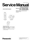
Model No. KX-PRL260B
KX-PRLA20
(Handset)
KX-PRL260W
KX-PRL262B
KX-PRL262W
KX-PRD260B
KX-PRD260W
KX-PRD262B
KX-PRD262W
KX-PRLA20B
KX-PRLA20W
KX-PRL260
(Base Unit)
KX-PRD260
(Base Unit)
(Charger Unit)
Configuration for each model
Model No
KX-PRL260
KX-PRL262
KX-PRD260
Base Unit
1 (PRL260)
1 (PRL260)
1 (PRD260)
Handset Charger Unit Expandable
1 (PRLA20)
Up to 6
1 (PRLA20)
1
Up to 6
1 (PRLA20)
Up to 6
KX-PRD262 1 (PRD260) 1 (PRLA20)
KX-PRLA20*
1 (PRLA20)
1
1
PRL series : Link-to-Cell Docking Station
for iPhone
PRD series : Link-to-Cell Docking Station
for Smartphone
B: Black Version
W: White Version
(for U.S.A.)
Up to 6
Up to 6
*KX-PRLA20 is also an optional accessory, which contains a
handset and a charger.
© Panasonic System Networks Co., Ltd. 2014
Unauthorized copying and distribution is a violation
of law.
KX-PRL260/KX-PRL262/KX-PRD260/KX-PRD262/KX-PRLA20
WARNING
This service information is designed for experienced repair technicians only and is not designed for use by the general
public. It does not contain warnings or cautions to advise non-technical individuals of potential dangers in attempting
to service a product. Products powered by electricity should be serviced or repaired only by experienced professional
technicians. Any attempt to service or repair the product or products dealt with in this service information by anyone
else could result in serious injury or death.
IMPORTANT SAFETY NOTICE
There are special components used in this equipment which are important for safety. These parts are marked by
in the Schematic Diagrams, Circuit Board Diagrams, Exploded Views and Replacement Parts List. It is essential that
these critical parts should be replaced with manufacturer’s specified parts to prevent shock, fire or other hazards.
Do not modify the original design without permission of manufacturer.
IMPORTANT INFORMATION ABOUT LEAD FREE, (PbF), SOLDERING
If lead free solder was used in the manufacture of this product, the printed circuit boards will be marked PbF.
Standard leaded, (Pb), solder can be used as usual on boards without the PbF mark.
When this mark does appear, please read and follow the special instructions described in this manual on the
use of PbF and how it might be permissible to use Pb solder during service and repair work.
L When you note the serial number, write down all 11 digits. The serial number may be found on the bottom of the unit.
L The illustrations in this Service Manual may vary slightly from the actual product.
2
KX-PRL260/KX-PRL262/KX-PRD260/KX-PRD262/KX-PRLA20
TABLE OF CONTENTS
PAGE
1 Safety Precautions----------------------------------------------- 5
1.1. For Service Technicians --------------------------------- 5
2 Warning -------------------------------------------------------------- 5
2.1. Battery Caution--------------------------------------------- 5
2.2. About Lead Free Solder (PbF: Pb free)-------------- 5
2.2.1. Suggested PbF Solder ------------------------------ 6
2.3. Discarding of P. C. Board-------------------------------- 6
3 Specifications ----------------------------------------------------- 7
4 Technical Descriptions ----------------------------------------- 8
4.1. US-DECT Description ------------------------------------ 8
4.1.1. TDD Frame Format ---------------------------------- 8
4.1.2. TDMA system------------------------------------------ 8
4.1.3. Signal Flowchart in the Radio Parts-------------- 9
4.2. Block Diagram (Base Unit_Main)---------------------10
4.3. Tel Interface Circuit--------------------------------------- 11
4.4. Block Diagram (Base Unit_RF Part) -----------------12
4.5. Circuit Operation (Base Unit) --------------------------13
4.5.1. BBIC (Base Band IC: IC501) ---------------------13
4.5.2. Flash Memory (IC502)------------------------------13
4.5.3. Flash Memory (IC601)------------------------------13
4.5.4. EEPROM (IC611) ------------------------------------13
4.5.5. Bluetooth Unit (IC721)------------------------------13
4.5.6. Power Supply Circuit/Reset Circuit--------------14
4.5.7. Telephone Line Interface---------------------------16
4.5.8. Parallel Connection Detect Circuit/Auto
Disconnect Circuit -----------------------------------17
4.5.9. Calling Line Identification (Caller ID)/Call
Waiting Caller ID -------------------------------------18
4.6. Block Diagram (Handset)-------------------------------20
4.7. Block Diagram (Handset_RF Part)-------------------21
4.8. Circuit Operation (Handset)----------------------------22
4.8.1. Outline --------------------------------------------------22
4.8.2. Power Supply Circuit/Reset Circuit--------------22
4.8.3. Charge Circuit ----------------------------------------23
4.8.4. Battery Low/Power Down Detector--------------23
4.8.5. Speakerphone ----------------------------------------23
4.9. Circuit Operation (Charger Unit) ----------------------23
5 Location of Controls and Components ------------------24
6 Installation Instructions ---------------------------------------24
7 Operating Instructions-----------------------------------------24
8 Test Mode ----------------------------------------------------------25
8.1. Engineering Mode ----------------------------------------25
8.1.1. Base Unit ----------------------------------------------25
8.1.2. Handset ------------------------------------------------27
9 Service Mode -----------------------------------------------------29
9.1. How to Clear User Setting (Handset Only)---------29
10 Troubleshooting Guide ----------------------------------------30
10.1. Troubleshooting Flowchart -----------------------------30
10.1.1. Check Power------------------------------------------31
10.1.2. Check Record ----------------------------------------32
10.1.3. Check Playback -------------------------------------35
10.1.4. Check Battery Charge ------------------------------35
10.1.5. Check Link---------------------------------------------36
10.1.6. Check the RF part -----------------------------------38
10.1.7. Registering a Handset to the Base Unit--------42
10.1.8. Deregistering a Handset ---------------------------42
10.1.9. Check Handset Transmission --------------------43
10.1.10. Check Handset Reception-------------------------43
11
12
13
14
15
3
PAGE
10.1.11. Check Caller ID ------------------------------------- 43
10.1.12. Check BT Communication ------------------------ 44
Disassembly and Assembly Instructions--------------- 46
11.1. Disassembly Instructions------------------------------- 46
11.1.1. Base Unit ---------------------------------------------- 46
11.1.2. Handset ------------------------------------------------ 48
11.1.3. Charger Unit ------------------------------------------ 49
11.2. How to Replace the Handset LCD------------------- 50
Measurements and Adjustments -------------------------- 51
12.1. Equipment Required ------------------------------------ 51
12.2. The Setting Method of JIG----------------------------- 51
12.2.1. Connections (Base Unit) -------------------------- 51
12.2.2. Connections (Handset) ---------------------------- 52
12.2.3. How to install Batch file into P.C. ---------------- 53
12.2.4. Commands-------------------------------------------- 54
12.3. Adjustment Standard (Base Unit) -------------------- 55
12.3.1. Bottom View ------------------------------------------ 55
12.4. Adjustment Standard (Handset) ---------------------- 56
12.4.1. Component View ------------------------------------ 56
12.5. Things to Do after Replacing IC or X'tal ------------ 57
12.5.1. How to download the data ------------------------ 57
12.6. Frequency Table------------------------------------------ 62
12.7. Bluetooth Frequency Table ---------------------------- 63
Miscellaneous---------------------------------------------------- 64
13.1. How to Replace the LLP (Leadless Leadframe
Package) IC ----------------------------------------------- 64
13.1.1. Preparation-------------------------------------------- 64
13.1.2. Caution------------------------------------------------- 64
13.1.3. How to Remove the IC ----------------------------- 64
13.1.4. How to Install the IC -------------------------------- 65
13.2. How to Replace the Flat Package IC --------------- 66
13.2.1. Preparation-------------------------------------------- 66
13.2.2. How to Remove the IC ----------------------------- 66
13.2.3. How to Install the IC -------------------------------- 67
13.2.4. How to Remove a Solder Bridge ---------------- 67
13.3. Terminal Guide of the ICs, Transistors and
Diodes ------------------------------------------------------ 68
13.3.1. Base Unit ---------------------------------------------- 68
13.3.2. Handset ------------------------------------------------ 68
Schematic Diagram -------------------------------------------- 69
14.1. For Schematic Diagram -------------------------------- 69
14.1.1. Base Unit (Schematic Diagram (Base
Unit_Main)) ------------------------------------------- 69
14.1.2. Handset
(Schematic
Diagram
(Handset_Main))------------------------------------- 69
14.2. Schematic Diagram (Base Unit_Main)-------------- 70
14.2.1. KX-PRL260/PRD260 ------------------------------- 70
14.3. Schematic Diagram (Handset_Main) --------------- 72
Printed Circuit Board ------------------------------------------ 74
15.1. Circuit Board (Base Unit_Main) ---------------------- 74
15.1.1. Component View ------------------------------------ 74
15.1.2. Bottom View ------------------------------------------ 75
15.2. Circuit Board (KEY)-------------------------------------- 76
15.2.1. Component View / Bottom View ----------------- 76
15.3. Circuit Board (MIC) -------------------------------------- 77
15.3.1. Component View / Bottom View ----------------- 77
15.4. Circuit Board (USB) ------------------------------------- 77
15.4.1. Component View / Bottom View ----------------- 77
KX-PRL260/KX-PRL262/KX-PRD260/KX-PRD262/KX-PRLA20
15.5. Circuit Board (Handset_Main) ------------------------ 78
15.5.1. Component View ------------------------------------ 78
15.5.2. Bottom View ------------------------------------------ 79
16 Exploded View and Replacement Parts List ----------- 80
16.1. Cabinet and Electrical Parts (Base Unit) ----------- 80
16.2. Cabinet and Electrical Parts (Handset) ------------- 81
16.3. Cabinet and Electrical Parts (Charger Unit) ------- 82
16.4. Accessories and Packing Materials ----------------- 83
16.4.1. Tools KX-PRL260/262, KX-PRD260/262------ 83
16.4.2. Tools KX-PRLA20 ----------------------------------- 84
16.5. Replacement Parts List --------------------------------- 85
16.5.1. Base Unit ---------------------------------------------- 85
16.5.2. Handset ------------------------------------------------ 88
16.5.3. Charger Unit ------------------------------------------ 89
16.5.4. Accessories and Packing Materials------------- 89
16.5.5. Screws ------------------------------------------------- 89
16.5.6. Fixtures and Tools----------------------------------- 89
4
KX-PRL260/KX-PRL262/KX-PRD260/KX-PRD262/KX-PRLA20
1 Safety Precautions
1.1.
For Service Technicians
• Repair service shall be provided in accordance with repair technology information such as service manual so as to
prevent fires, injury or electric shock, which can be caused by improper repair work.
1. When repair services are provided, neither the products nor their parts or members shall be remodeled.
2. If a lead wire assembly is supplied as a repair part, the lead wire assembly shall be replaced.
3. FASTON terminals shall be plugged straight in and unplugged straight out.
• ICs and LSIs are vulnerable to static electricity.
When repairing, the following precautions will help prevent recurring malfunctions.
1. Cover plastic parts boxes with aluminum foil.
2. Ground the soldering irons.
3. Use a conductive mat on worktable.
4. Do not grasp IC or LSI pins with bare fingers.
2 Warning
2.1.
Battery Caution
Risk of explosion if battery is replaced by an incorrect type. Dispose of used batteries according to the instructions.
Attention:
A nickel metal hydride battery that is recyclable powers the product you have purchased.
Please call 1-800-8-BATTERY (1-800-822-8837) for information on how to recycle this battery.
2.2.
About Lead Free Solder (PbF: Pb free)
Note:
In the information below, Pb, the symbol for lead in the periodic table of elements, will refer to standard solder or solder that
contains lead.
We will use PbF solder when discussing the lead free solder used in our manufacturing process which is made from Tin (Sn),
Silver (Ag), and Copper (Cu).
This model, and others like it, manufactured using lead free solder will have PbF stamped on the PCB. For service and repair
work we suggest using the same type of solder.
Caution
• PbF solder has a melting point that is 50 F ~ 70 F (30 C ~ 40 C) higher than Pb solder. Please use a soldering iron with
temperature control and adjust it to 700 F ± 20 F (370 C ± 10 C).
• Exercise care while using higher temperature soldering irons.:
Do not heat the PCB for too long time in order to prevent solder splash or damage to the PCB.
• PbF solder will tend to splash if it is heated much higher than its melting point, approximately 1100 F (600 C).
• When applying PbF solder to double layered boards, please check the component side for excess which may flow onto the
opposite side (See the figure below).
Remove all of the
excess solder
Component
pin
Solder
(Slice View)
5
Component
KX-PRL260/KX-PRL262/KX-PRD260/KX-PRD262/KX-PRLA20
2.2.1.
Suggested PbF Solder
There are several types of PbF solder available commercially. While this product is manufactured using Tin, Silver, and Copper
(Sn+Ag+Cu), you can also use Tin and Copper (Sn+Cu), or Tin, Zinc, and Bismuth (Sn+Zn+Bi). Please check the
manufacturer's specific instructions for the melting points of their products and any precautions for using their product with other
materials.
The following lead free (PbF) solder wire sizes are recommended for service of this product: 0.3 mm, 0.6 mm and 1.0 mm.
0.3 mm X 100 g
2.3.
0.6 mm X 100 g
1.0 mm X 100 g
Discarding of P. C. Board
When discarding P. C. Board, delete all personal information such as telephone directory and caller list or scrap P. C. Board.
6
KX-PRL260/KX-PRL262/KX-PRD260/KX-PRD262/KX-PRLA20
3 Specifications
█ Standard:
DECT 6.0 (Digital Enhanced Cordless
Telecommunications 6.0)
Bluetooth wireless technology 2.1+EDR
█ Number of channels:
60 Duplex Channels (DECT)
79 Duplex channels(Bluetooth)
█ Frequency range:
1.92 GHz to 1.93 GHz (DECT)
2.402 GHz to 2.48 GHz (Bluetooth)
█ Duplex procedure:
TDMA (Time Division Multiple Access)
█ Channel spacing:
1.728 MHz (DECT)
1.0 MHz(Bluetooth)
Power source
Receiving Method
Oscillation Method
Detecting Method
Tolerance of OSC Frequency
Modulation Method
ID Code
Ringer Equivalence No. (REN)
Dialing Mode
Redial
Speed Dialer
Power Consumption
Operating Conditions
Dimensions (W x D x H)
Mass (Weight)
█ Bit rate:
1.152 Mbit/s (DECT)
1.0 Mbit/s (Bluetooth)
█ Modulation:
GFSK (Gaussian Frequency Shift Keying)
█ RF transmission power:
115 mW (max)
█ Voice coding:
ADPCM 32 kbit/s (DECT)
CVSD/PCM 64 kbit/s (Bluetooth)
PCM 64 kbit/s(BT_IC)
Base Unit
Handset
Charger
AC Adaptor
(PNLV238-KZ, 120 V AC, 60 Hz)
Super Heterodyne
PLL synthesizer
Quadrature Discriminator
10.368 MHz ±100 Hz
Frequency Modulation
40 bit
0.1 B
Tone (DTMF)/Pulse
Up to 48 digits
Up to 24 digits (Phonebook)
Standby: Approx. 1.1 W
Maximum: Approx. 13.5 W
0 °C - 40 °C (32 °F – 104 °F)
20 % – 80 % relative air humidity
(dry)
Approx. 160 mm x 100 mm x 115 mm
for KX-PRL262,PRD262
Approx. 330 g
for KX-PRL262,PRD262
Rechargeable Ni-MH battery
AAA (R03) size (1.2 V 400 mAh)
Super Heterodyne
PLL synthesizer
Quadrature Discriminator
10.368 MHz ±100 Hz
Frequency Modulation
40 bit
AC Adaptor
(PNLV233Z, 120 V AC, 60 Hz)
Tone (DTMF)/Pulse
Up to 48 digits
Up to 24 digits (Phonebook)
6 days at Standby,
10 hours at Talk
0 °C - 40 °C (32 °F – 104 °F)
20 % – 80 % relative air humidity
(dry)
Approx. 45 mm x 23 mm x 155 mm
Approx. 110 g
Note:
Design and specifications are subject to change without notice.
Note for Service:
• Operation range: Up to 300 m outdoors, Up to 50 m indoors, depending on the condition.
• Analog telephone connection: Telephone Line
• Optional Range extender: KX-TGA405
• Optional Key detector: KX-TGA20
• T-adaptor: KX-J66
7
Standby: Approx 0.1 W
Maximum: Approx 1.8 W
0 °C - 40 °C (32 °F – 104 °F)
20 % – 80 % relative air humidity
(dry)
Approx. 70 mm x 70 mm x 40 mm
Approx. 50 g
KX-PRL260/KX-PRL262/KX-PRD260/KX-PRD262/KX-PRLA20
4 Technical Descriptions
4.1.
US-DECT Description
The frequency range of 1.92 GHz-1.93 GHz is used. Transmitting and receiving carrier between base unit and handset is same
frequency. Refer to Frequency Table (P.62).
4.1.1.
TDD Frame Format
RX1
5 ms
5 ms
Up Link ( Handset -> Base Unit )
Down Link ( Base Unit -> Handset )
RX2
RX3
RX4
RX5
RX6
TX1
TX2
TX3
TX4
TX5
TX6
DATA rate : 1.152 Mbps
417 μs (available) 417 μs (blind)
4.1.2.
TDMA system
This system is the cycles of 10 ms, and has 6 duplex paths, but maximum duplex communication path is 5 because of dummy
bearer use.
In 1 slot 417 s, the 10 ms of voice data is transmitted.
• 2 - Handsets Link
Traffic Bearer
Base unit
Handset 1
(Stand by)
Handset 2
(Link)
Handset 3
(Link)
Dummy bearer
RX1 RX2 RX3 RX4 RX5 RX6 TX1 TX2 TX3 TX4 TX5 TX6
TX
RX
TX
RX
Traffic Bearer
A link is established between base unit and handset.
The state where duplex communication is performed.
Handset doesn't make up duplex in no free RF channels because of interference. (*1)
Dummy Bearer
Base unit sends Dummy-data to the all stand-by state handsets.
Handsets receive that data for synchronization and monitoring request from the base unit.
Base unit doesn't send Dummy bearer in no free RF channels because of interference. (*1)
Note:
(*1) It is a feature under FCC 15 regulation and for interference avoidance.
In the case of checking RF parts, it is better in least interference condition.
8
KX-PRL260/KX-PRL262/KX-PRD260/KX-PRD262/KX-PRLA20
4.1.3.
Signal Flowchart in the Radio Parts
Reception
Base unit:
A voice signal from TEL line is encoded to digital data and converted into a 1.9 GHz modulated radio signal by BBIC(IC501).
The RF signal, after which is amplified in BBIC, is fed to selected antenna.
Handset:
As for a handset RF, RF signal is received in one antenna.
BBIC down-converts to 864 kHz IF signal from RX signal and demodulates it to digital data "RXDATA".
BBIC (IC1) converts RXDATA into a voice signal and outputs it to speaker.
Transmission
Handset:
A voice signal from microphone is encoded to digital data and converted into a 1.9 GHz modulated radio signal by BBIC(IC1).
The RF signal, after which is amplified in BBIC, is fed to an antenna.
Base unit:
As for a base unit RF, RF signal is received in two antennas.
BBIC (IC501) compares RF signal levels and selects the antenna to be used. Then BBIC down-converts to 864 kHz IF signal
from RX signal in the selected antenna, and demodulates it to digital data "RXDATA".
BBIC (IC501) converts RXDATA into a voice signal and outputs it to TEL line.
9
+5.0V
IC401
IC402
ANT2
10
IC722
BT_1.8V
IC721
BT Module
RF_Block
IC601
BBIC
IC501
RF_VDD
VDD_PA
IC611
KEY
PAD
VBAT
PDN_DET
CHARGE_DET
VRF
/VPA
AVD/VDD
QSPI
CIDINp
CIDINn
LSRp
MICh
P3_6
IC502
Crystal
10.368MHz
Q701
CHARGE
DETECT
Q301
+3.0V
+5.0V
1
4
Power Down
DET
IC411
D101
2
3
Power supply
at AC failure
IC302
REGULATOR
Q141
TR_RLY
KX-PRL260/262, KX-PRD260/262 BLOCK DIAGRAM (Base Unit_Main)
+1.8V
SIDE_TONE
CIRCUIT
Q161
-
+
CHARGE
GND
DC_JACK
DC5.5V+
RING
TIP
TEL_JACK
4.2.
LED
KX-PRL260/KX-PRL262/KX-PRD260/KX-PRD262/KX-PRLA20
Block Diagram (Base Unit_Main)
RX AMP
TX AMP
SIDE TONE
CONTROL
CIRCUIT
R142
11
REGULATOR
CALLER ID
DETECT
BELL
DETECT
1
4
C102
2
3
D101
C101
R104 C106
R102 C104
R103 C105
R101 C103
SA101
R141
P101
RING
TIP
4.3.
Q141
KX-PRL260/KX-PRL262/KX-PRD260/KX-PRD262/KX-PRLA20
Tel Interface Circuit
ANT2
RF_RXp
RF_RXn
RF_TXp
RF_TXn
12
Demodulator
Control
Logic
RXDATA
TXDATA
10.368
MHz
KX-PRL260/262,KX-PRD260/262 BLOCK DIAGRAM (Base Unit_RF Part)
Mixer
Modulator
PLL
3856-3843MHz
/3859-3845MHz
4.4.
IC501 RF block
KX-PRL260/KX-PRL262/KX-PRD260/KX-PRD262/KX-PRLA20
Block Diagram (Base Unit_RF Part)
KX-PRL260/KX-PRL262/KX-PRD260/KX-PRD262/KX-PRLA20
4.5.
Circuit Operation (Base Unit)
General Description:
(BBIC, Flash Memory, EERROM) is a digital speech/signal processing system that implements all the functions of speech
compression, record and playback, and memory management required in a digital telephone answering machine.
The BBIC system is fully controlled by a host processor. The host processor provides activation and control of all that functions
as follows.
PCM OUT
Bluetooth Unit
PCM IN
ADPCM
TDD & TDMA
with FHSS
Processor
ADPCM
Digital
Speech
Processor
RF part
Caller ID
Modem
BBIC (IC501)
4.5.1.
Flash Memory
(Program)
IC502
Multiplexer
MIC
IC402
Digital TAM System
Keys/ LEDs
/ Charge
TEL
Line
Interface
&
Host CPU
EEPROM
IC611
Analog
Front
End
IC401
Dock SP
Flash Memory IC601
BBIC (Base Band IC: IC501)
• Voice Message Recording/Play back
The BBIC system uses a proprietary speech compression technique to record and store voice message in Flash Memory.
An error correction algorithm is used to enable playback of these messages from the Flash Memory.
• DTMF Generator
When the DTMF data from the handset is received, the DTMF signal is output.
• Synthesized Voice (Pre-recorded message)
The BBIC implements synthesized Voice, utilizing the built in speech detector and a Flash Memory, which stored the vocabulary.
• Caller ID demodulation
The BBIC implements monitor and demodulate the FSK/DTMF signals that provide CID information from the Central Office.
• Digital Switching
The voice signal from telephone line is transmitted to the handset or the voice signal from the handset is transmitted to the
Telephone line, etc. They are determined by the signal path route operation of voice signal.
• Block Interface Circuit
RF part, LED, Key scan, Speaker, Telephone line.
4.5.2.
Flash Memory (IC502)
Main program data is stored.
4.5.3.
Flash Memory (IC601)
Following information data is stored.
• Voice signal
ex: Pre-recorded Greeting message, Incoming message
4.5.4.
EEPROM (IC611)
Following information data is stored.
• Settings
ex: message numbers, ID code, Flash Time, Tone/Pulse
4.5.5.
Bluetooth Unit (IC721)
Use for Bluetooth communication.
13
KX-PRL260/KX-PRL262/KX-PRD260/KX-PRD262/KX-PRLA20
4.5.6.
Power Supply Circuit/Reset Circuit
The power supply voltage from AC adaptor is converted to VBAT (3.0V) in IC302. And +3.0V for peripherals and analog part is
insulated from VBAT by Doubler of BBIC.
Circuit Operation:
+5.5V
+5.5V
AC Adaptor
+3.0V
VDD2
VDD4
IC501
IC302
IC611
+3.0V_CP
+3.0V
EEPROM
3.0V
REGULATOR
VDD1
Q301
BBIC
VDD5
+3.0V_CP2
+1.8V
IC601
TAM FLASH
IC502
QSPI FLASH
RF Part
LEDs
IC721
IC722
+1.8V
Bluetooth
unit
VDD3
IC411
IC401
5.0V
REGULATOR
D-AMP
VBAT
1.8 V
Reset (RSTN)
(IC501_77pin)
Startmonitor
(IC501 57pin)
(CKM/STM)
BBIC chip initialize
14
KX-PRL260/KX-PRL262/KX-PRD260/KX-PRD262/KX-PRLA20
4.5.6.1.
Charge Circuit
+5.5V
A
F301
DCP
R373
K
D362
R372 R371
The voltage from the AC adaptor is supplied to the charge circuits.
CHARGE+
DCM
C351
CHARGE-
15
KX-PRL260/KX-PRL262/KX-PRD260/KX-PRD262/KX-PRLA20
4.5.7.
Telephone Line Interface
Telephone Line Interface Circuit:
Function
• Bell signal detection
• ON/OFF hook and pulse dial circuit
• Side tone circuit
Bell (RINGING) signal detection and OFF HOOK circuit:
In the idle mode, Q141 is open to cut the DC loop current and decrease the ring load. When ring voltage appears at the Tip (T)
and Ring (R) leads (When the telephone rings), the AC ring voltage is transferred as follows:
L1T C105 R103 R110 R111 R112 BBIC pin18(RINGING)
When the CPU (BBIC) detects a ring signal, Q141 turns on, thus providing an off-hook condition (active DC current flow through
the circuit). Following signal flow is the DC current flow.
T D101 Q141 Q161 R163 D101 P101 R
ON HOOK Circuit:
Q141 is open, Q141 is connected as to cut the DC loop current and to cut the voice signal. The unit is consequently in an onhook condition.
Pulse Dial Circuit:
Pin 19 of BBIC turns Q141 ON/OFF to make the pulse dialing.
Side Tone Circuit:
Basically this circuit prevents the TX signal from feeding back to RX signal. As for this unit, TX signal feed back from Q161 is
canceled by the canceller circuit of BBIC.
C173
E
C
B
Q161
B
R141
E
K
A
D142
C142
R164
C101
Q142
R151
C
B
R142
R145
C152
R152
R163
R166
C171
_
~
3
+
~
C174
OFF Hook
D101
E
4
L1T
2
1
SA101
R178
RX
Pin25 of IC501
C
Q141
R162
R165
C167
+
R168
C161
R160
L1R
C102
TX
Pin27 of IC501
C184
HOOK
Pin19 of IC501
PARADET
Pin17 of IC501
ADC1
Pin33 of IC501
R110
R111
C110
CIDOUT
Pin24 of IC501
C111
C113
R112
R101 C103
BELL signal detection
CIDINn
Pin23 of IC501
R116
R118
RINGING
Pin18 of IC501
C116
C115
ADC0
Pin32 of IC501
R117
R115
R103
C105
R102 C104
CIDINp
Pin21 of IC501
C109
R104 C106
LSRn
Pin28 of IC501
R109
16
P101
KX-PRL260/KX-PRL262/KX-PRD260/KX-PRD262/KX-PRLA20
4.5.8.
Parallel Connection Detect Circuit/Auto Disconnect Circuit
Function:
In order to disable call waiting and stutter tone functions when using telephones connected in parallel, it is necessary to have a
circuit that judges whether a telephone connected in parallel is in use or not. This circuit determines whether the telephone
connected in parallel is on hook or off hook by detecting changes in the T/R voltage.
Circuit Operation:
Parallel connection detection when on hook:
When on hook, the voltage is monitored at pin 32 of IC501. There is no parallel connection if the voltage is
0.54 V or higher, while a parallel connection is deemed to exist if the voltage is lower.
Parallel connection detection when off hook:
When off hook, the voltage is monitored at pin 17 of IC501; the presence/absence of a parallel connection is determined by
detecting the voltage changes.
If the Auto disconnect function is ON and statuses are Hold, receiving ICM, OGM transmitting, BBIC disconnects the line after
detecting parallel connection is off hook.
B
B
R141
A
D142
C142
R164
K
E
Q142
R151
C101
C
D101
R145
C152
R152
R163
R166
3
+
_
~
C171
E
~
C174
B
4
L1T
2
1
SA101
C173
Q161
R142
R178
RX
Pin25 of IC501
C
R162
R165
C167
+
R168
C161
C
E
Q141
R160
L1R
C102
TX
Pin27 of IC501
C184
HOOK
Pin19 of IC501
PARADET
Pin17 of IC501
R115
17
R118
C116
R117
ADC0
Pin32 of IC501
C115
ADC1
Pin33 of IC501
R116
P101
KX-PRL260/KX-PRL262/KX-PRD260/KX-PRD262/KX-PRLA20
4.5.9.
Calling Line Identification (Caller ID)/Call Waiting Caller ID
Function:
Caller ID
The caller ID is a chargeable ID which the user of a telephone circuit obtains by entering a contract with the telephone company
to utilize a caller ID service. For this reason, the operation of this circuit assumes that a caller ID service contract has been
entered for the circuit being used. The data for the caller ID from the telephone exchange is sent during the interval between the
first and second rings of the bell signal. The data from the telephone exchange is a modem signal which is modulated in an FSK
(Frequency Shift Keying) * format. Data "1" is a 1200 Hz sine wave, and data "0" is a 2200 Hz sine wave. There are two types of
the message format which can be received: i.e. the single message format and plural message format. The plural message
format allows to transmit the name and data code information in addition to the time and telephone number data.
*: Also the telephone exchange service provides other formats.
Single message format
1st Ring
2 sec
2nd Ring
2 sec
Silent interval 4 sec
0.5 s 575 ms
min 0.5 s
DATA
STD Ring / 20 Hz
Tip-Ring
0.1 Vrms
70 Vrms
A
DATA in
2200 Hz
=DATA "0 "
1200 Hz
=DATA "1"
B
DATA out
1 bit=833 µs
month
04
day
15
hour
16
minute
35
number
2013487000
Plural message format
1st Ring
2 sec
0.5 s
718 ms
2nd Ring
DATA
DATA CODE NAME
201
John Smith
month
04
day
16
18
hour
16
minute
35
number
2013487000
KX-PRL260/KX-PRL262/KX-PRD260/KX-PRD262/KX-PRLA20
Call Waiting Caller ID
Calling Identity Delivery on Call Waiting (CIDCW) is a CLASS service that allows a customer, while off-hook on an existing call,
to receive information about a calling party on a waited call. The transmission of the calling information takes place almost
immediately after the customer is alerted to the new call so he/she can use this information to decide whether to take the new
call.
Function:
The telephone exchange transmits or receives CAS and ACK signals through each voice RX/TX route. Then FSK data and
MARK data pass the following route.
Telephone Line P101 C105, C104 R103, R102 IC501(23, 21).
If the unit deems that a telephone connected in parallel is in use, ACK is not returned even if CAS is received, and the
information for the second and subsequent callers is not displayed on the portable handset display.
Call Waiting Format
CAS: CPE Alerting Signal
Dual Tone of 2130 Hz, 2750 Hz
-15 dBm (900 ohm load)
Signal Flow
Telephone Exchange
Cordless phone
Continuance Signal
of 1200 Hz (Data "1")
"FSK"
MARK
CAS
80 5 ms
DATA
0~500 ms 58~75 ms
about 300 ms
(be changed by
Information Volume)
ACK: Acknowledged Signal
DTMF
"D"
Signal Flow
Cordless phone
Telephone Exchange
ACK
R110
CIDOUT
Pin 24
C110
0~100 ms 60 5 ms
R101 C103
R103 C105
IC501
R102 C104
CIDINp
Pin 21
R109
R104 C106
C109
LSRn
Pin 28
L1T
SA101
CIDINn
Pin 23
19
L1R
P101
KX-PRL260/KX-PRL262/KX-PRD260/KX-PRD262/KX-PRLA20
4.6.
Block Diagram (Handset)
3V
IC4
IC3
FLASH
MEMORY
ANT1
X1
10.368 MHz
EEPROM
WP, CLK, DATA
QSPI_100~4
QSPI_CS,
QSPI_SCK1
VBAT
CHG_DET
RXp
RXn
CHARGE
CONTROL
TXp
TXn
RST
RSTN
RF part
CHARGE
CHG_CTL
POWER SUPPLY
CONTROL
BATTERY_ON
VBAT
IC1
MIC
BATTERY
BBIC
MICp
MICn
Receiver
LSRp
LSRn
4V
LED
(KEY)
Q6
KIN_1~4
CKM/STM
4V
PAOUTp
PAOUTn
CKM//
NR_LED
SP-PHONE SP
STB_A~F
KEY_LED
STM
LED
(LCD)
LCD
KEYS
KX-PRLA20 BLOCK DIAGRAM (Handset)
20
KX-PRL260/KX-PRL262/KX-PRD260/KX-PRD262/KX-PRLA20
4.7.
Block Diagram (Handset_RF Part)
TXp
TXn
ANT
RXp
RXn
KX-PRLA20 BLOCK DIAGRAM (Handset_RF Part)
21
KX-PRL260/KX-PRL262/KX-PRD260/KX-PRD262/KX-PRLA20
4.8.
4.8.1.
Circuit Operation (Handset)
Outline
Handset consists of the following ICs as shown in Block Diagram (Handset) (P.20).
• DECT BBIC (Base Band IC): IC1
- All data signals (forming/analyzing ACK or CMD signal)
- All interfaces (ex: Key, Detector Circuit, Charge, EEPROM, LCD)
• EEPROM: IC3
- Setting data is stored. (e.g. ID, user setting)
4.8.2.
Power Supply Circuit/Reset Circuit
Circuit Operation:
When powering on the Handset, the voltage is as follows;
BATTERY(2.2 V ~ 2.6 V: BATT+) F1 BBC1 (IC1) 10 pin
The Reset signal generates IC1 (54 pin) and 1.8 V.
VBAT
1.8 V
Reset (*RST)
(IC1_71 pin)
Start monitor
(IC1 50 pin)
(STM)
BBIC chip initialize
VBAT
Charge Pump Output
For all peripherals
4.0V
3.0V
3.0V
BATTERY
2CELL
EEPROM
GND
1.8V
4.0V
BBIC
3.0V
1.8V
LCD
4.0V
KEY LED
GND
22
KX-PRL260/KX-PRL262/KX-PRD260/KX-PRD262/KX-PRLA20
4.8.3.
Charge Circuit
Circuit Operation:
When charging the handset on the Base Unit, the charge current is as follows;
DCP(5.5 V) F301 R371 R372 D362 CHARGE+(Base) CHARGE+(Handset) R8 Q3 F1
BATTERY+... Battery...
BATTERY- R45 GND CHARGE-(Handset) CHARGE-(Base) GND DC-(GND)
In this way, the BBIC on Handset detects the fact that the battery is charged.
The charge current is controlled by switching Q9 of Handset.
Refer to Fig.101 in Power Supply Circuit/Reset Circuit (P.14).
Q2
C27
R9
R2
R8
CHG +
Q3
R4
BATT +
Q4
47K
BATTERY
2CELL
R6
10K
CHG -
BATT R45
Q9
GND
GND
GND
CHG CTRL (33)
R7
CHG DET (34)
BBIC
IC1
100K
4.8.4.
Battery Low/Power Down Detector
Circuit Operation:
“Battery Low” and “Power Down” are detected by BBIC which check the voltage from battery.
The detected voltage is as follows;
• Battery Low
Battery voltage: V(Batt) 2.25 V ± 50 mV
The BBIC detects this level and "
" starts flashing.
• Power Down
Battery voltage: V(Batt) 2.0 V ± 50 mV
The BBIC detects this level and power down.
4.8.5.
Speakerphone
The hands-free loudspeaker at SP+ and SP- is used to generate the ring alarm.
4.9.
Circuit Operation (Charger Unit)
Charge control is executed at handset side so that the operation when using charger is also controlled by handset.
Refer to Circuit Operation (Handset) (P.22)
TP1
J1
TP2
AC Adaptor
The route for this is as follows: DC+pin of J1(+) CHARGE+pad Handset CHARGE-pad DC-pin of J1(-).
23
KX-PRL260/KX-PRL262/KX-PRD260/KX-PRD262/KX-PRLA20
5 Location of Controls and Components
Refer to the Operating Instructions.
Note:
You can download and refer to the Operating Instructions (Instruction book) on TSN Server.
6 Installation Instructions
Refer to the Operating Instructions.
Note:
You can download and refer to the Operating Instructions (Instruction book) on TSN Server.
7 Operating Instructions
Refer to the Operating Instructions.
Note:
You can download and refer to the Operating Instructions (Instruction book) on TSN Server.
24
KX-PRL260/KX-PRL262/KX-PRD260/KX-PRD262/KX-PRLA20
8 Test Mode
8.1.
Engineering Mode
8.1.1.
Base Unit
Important:
Make sure the address on LCD is correct when entering new data. Otherwise, you may ruin the unit.
OFF
Dial keypad
This pictured model is KX-PRL260
FLASH
CALL WAIT
H/S LCD
H/S key operation
1). PressMENU.
2). Select "Settings" using
then pressSELECT.
Select "Set tel line" using
then pressSELECT.
or
or
3). Enter "7", "2", "6", "2", "7", "6", "6", "4".
Note: 7262 7664 = PANA SONI
(see letters printed on dial keys)
4). Select "Write EEP" using
then pressSELECT.
Service Mode
Read EEP
Write EEP
5). Enter ""ە, ""ە, ""ە, "( "ەAddress). (*1)
BACK
SELECT
Set Addr.:
Default Data
6). Enter "㸨", "㸨" (New Data). (*1)
CLEAR
25
OK
KX-PRL260/KX-PRL262/KX-PRD260/KX-PRD262/KX-PRLA20
Set Addr.:
7). Press OK , a long confirmation beep
will be heard.
New Data
CLEAR
8). Press OFF to return to standby mode.
After that, turn the base unit power off and then power on.
Note: * To enter "Set dial mode", pressSELECT
SELECT at " Set tel line".
It is necessary to turn on the power of base unit.
OK
Set Addr.:
____ __
BACK
* "Set tel line" isn't displayed in Cell line only mode.
To return to normal mode, execute the following procedure:
1
2
3
MENU
or
→
#
1
5
7
: Select "off " → SELECT
OFF
Frequently Used Items (Base Unit)
ex.)
Items
Frequency
ID
Address
00 07 / 00 08
00 02 ~ 00 06
Default Data
70/02
Given value
New Data
-
-
Remarks
Use these items in a READ-ONLY mode to
confirm the contents. Careless rewriting may
cause serious damage to the computer system.
Note:
(*1) When you enter the address or New Data, please refer to the table below.
Desired Number (hex)
0
1
.
.
.
9
Input Keys
0
1
.
.
.
9
Desired Number (hex)
A
B
C
D
E
F
26
Input Keys
[Flash] + 0
[Flash] + 1
[Flash] + 2
[Flash] + 3
[Flash] + 4
[Flash] + 5
KX-PRL260/KX-PRL262/KX-PRD260/KX-PRD262/KX-PRLA20
8.1.2.
Handset
Important:
Make sure the address on LCD is correct when entering new data. Otherwise, you may ruin the unit.
OFF
Dial keypad
FLASH
CALL WAIT
H/S key operation
H/S LCD
1). PressMENU.
2). Select "Settings" using
then press SELECT.
or
3). Enter "7", "2", "6", "2", "7", "6", "6", "4".
Note: 7262 7664 = PANA SONI
(see letters printed on dial keys)
4). Select "Write EEP" using
then press SELECT.
or
Service Mode
Read EEP
Write EEP
BACK
5). Enter ""ە, ""ە, ""ە, "( "ەAddress). (*1)
SELECT
Set Addr.:
Default Data
CLEAR
6). Enter "㸨", "㸨" (New Data). (*1)
OK
Set Addr.:
New Data
7). Press OK , a long confirmation beep
will be heard.
CLEAR
OK
Set Addr.:
____
__
BACK
8). Press OFF to return to standby mode.
After that, remove and reinsert the batteries. Press the Power button for
about 1 second if the power is not turned on.
27
KX-PRL260/KX-PRL262/KX-PRD260/KX-PRD262/KX-PRLA20
Frequently Used Items (Handset)
ex.)
Items
Address
Default Data
New Data
Frequency
ID
00 07 / 00 08
00 02 ~ 00 06
00 / 01
Given value
-
Possible Adjusted
Value MAX (hex)
-
Possible Adjusted
Value MIN (hex)
-
Remarks
(*2)
Note:
(*1) When you enter the address or New Data, please refer to the table below.
Desired Number (hex.)
0
1
.
.
.
9
Input Keys
0
1
.
.
.
9
Desired Number (hex.)
A
B
C
D
E
F
Input Keys
[Flash] + 0
[Flash] + 1
[Flash] + 2
[Flash] + 3
[Flash] + 4
[Flash] + 5
(*2) Use these items in a READ-ONLY mode to confirm the contents. Careless rewriting may cause serious damage to the
handset.
28
KX-PRL260/KX-PRL262/KX-PRD260/KX-PRD262/KX-PRLA20
9 Service Mode
9.1.
How to Clear User Setting (Handset Only)
Handset
Press
, , ,
simultaneously until a beep sound is heard. Then single handset is initialized.
(The contents of user setting are reset to factory default)
*Usage time is not cleared.
29
KX-PRL260/KX-PRL262/KX-PRD260/KX-PRD262/KX-PRLA20
10 Troubleshooting Guide
10.1. Troubleshooting Flowchart
FLOW CHART
Not working
Power ON Base Unit
Check Power
OK
Not recording (*1)
Record
Check Record
OK
Playback Pre-Message
No playback
Check Playback
OK
Link
No link
Battery Charge
OK
Not charged
Check Battery Charge
OK
Check Link
NG
Range
Check the RF part
OK
Handset Voice Transmission
No voice
Check Handset Transmission
OK
Handset Voice Reception
No voice
Check Handset Reception
OK
Caller ID function
Caller ID Error
Check Caller ID
OK
Bluetooth Function
NG
Check BT Communication
Cross Reference:
Check Power (P.31)
Check Record (P.32)
Check Playback (P.35)
Check Battery Charge (P.35)
Check Link (P.36)
Check the RF part (P.38)
Check Handset Transmission (P.43)
Check Handset Reception (P.43)
Check Caller ID (P.43)
Check BT Communication (P.44)
Note:
(*1) When a user claims that the unit disconnects a call right
after the greeting message and no incoming messages can
be recorded, this symptom can not reappear with TEL
simulator in the service center. In this case, try to change
the Auto disconnect activation time and Vox level.
<How to change the Auto Disconnect activation time
and VOX level> (P.33) item (A) and (B).
30
KX-PRL260/KX-PRL262/KX-PRD260/KX-PRD262/KX-PRLA20
10.1.1. Check Power
10.1.1.1. Base Unit
Is the AC Adaptor inserted into AC outlet? (*1)
Is output voltage of AC adaptor 5.5 V?
NO
Check AC Adaptor.
YES
Check VDD1(1.8 V) :Test point (VDD1)
NO
Check Power Supply Circuit.
OK
RSTN: Reset = "High"?
NO
Check Reset Circuit.
YES
Check Xtal CLK=10.368 MHz?
NO
Check X501.
YES
Check BBIC.
Cross Reference:
Power Supply Circuit/Reset Circuit (P.14)
Note:
BBIC is IC501.
(*1) Refer to Specifications (P.7) for part number and
supply voltage of AC adaptor.
(*2) Refer to Circuit Board (Base Unit_Main) (P.74).
10.1.1.2. Handset
Is the battery inserted to BATT+ and BATT-?
YES
NO
Check the battery and around BATT+ and
BATT- are not shorted.
Is the voltage of TP-VBAT 2.3 V more?
YES
NO
Check Power Supply Circuit/Reset Circuit.
Is the voltage of TP 1.8V about 1.8 V?
YES
NO
Does BBIC (IC1: 49) oscillate at 10.368 MHz?
Check X1, C52, C53.
YES
Check BBIC (IC1).
Cross Reference:
Power Supply Circuit/Reset Circuit (P.22)
31
KX-PRL260/KX-PRL262/KX-PRD260/KX-PRD262/KX-PRLA20
10.1.2. Check Record
10.1.2.1. Base Unit
Not record Incoming Message
NO
Check Bell signal.
OK
Does the unit catch line?
NO
YES
Check Line In: Pin 25 of BBIC.
NO
Check Telephone Line Interface
[Bell].
Check Telephone Line Interface
[OFF HOOK].
Check ICM Recording in Signal Route.
OK
Check Auto Disconnect Circuit.
OK
Check Parallel Connection Detection
Circuit.
OK
Check BBIC and Flash Memory.
Note:
Flash Memory is IC601.
BBIC is IC501.
Cross Reference:
Telephone Line Interface (P.16)
Parallel Connection Detect Circuit/Auto Disconnect
Circuit (P.17)
32
KX-PRL260/KX-PRL262/KX-PRD260/KX-PRD262/KX-PRLA20
<How to change the Auto Disconnect activation time and VOX level>
A) Auto Disconnect activation time:
Some Telephone Company lines (fiber or cable) ON Hook and OFF Hook voltages are lower than conventional lines, which may
cause a malfunction of Auto Disconnect detection. To solve this problem, try changing the Auto Disconnect activation through
the procedures below.
1) Press "MENU " key at standby Mode and "#" key.
Note: The set must power on and be linked.
2) Press "9", "0", "0", "0"," " .
LCD (H/S)
Service ready
:
BACK
3) Press "7","3","1".
Service ready
:7 3 1
CLEAR
4) Then enter the below last digit;
last digit
Auto disconnect & CPC
"0"
(*1)
: enable 㨇default㨉
(*1)
Auto disconnect : enable
"1"
"2"
CPC : disable
Auto disconnect & CPC
(*2)
: disable
Note:
(*1) Both Auto Disconnect and CPC don't detect for the first 2 seconds.
(*2) If the "Disable" is selected, even if the parallel-connected telephone is OFF HOOK,
the line isn't disconnected.
5) Back to "standby" mode automatically after step 4).
You can hear beep sound which is a confirmation tone.
33
KX-PRL260/KX-PRL262/KX-PRD260/KX-PRD262/KX-PRLA20
B) Vox level:
It makes easier to detect a small voice (caller) by raising the sensitivity of VOX level. Therefore, the recording of TAM is not
turned off during detection.
1) ~ 2) are same as (A).
3) Press "5","1","1".
Service ready
:5 1 1
CLEAR
4) Then enter the below last digit;
last digit
default setting
"0"
"1"
: normal
6dB up
5) Back to "standby" mode automatically after step 4.
You can hear beep sound which is a confirmation tone.
34
KX-PRL260/KX-PRL262/KX-PRD260/KX-PRD262/KX-PRLA20
10.1.3. Check Playback
10.1.3.1. Base Unit
Check VDD1(1.8 V) :Test point (VDD1)
NO
Check Power Supply Circuit.
OK
Check output of BBIC (Pin 73,74).
NO
Check BBIC and Flash Memory.
OK
Check VDD3(5.0 V):Test Point (VDD3).
NO
Check IC411
OK
Check Speaker and its surroundings.
Cross Reference:
Power Supply Circuit/Reset Circuit (P.14)
Note:
Flash Memory is IC601.
BBIC is IC1.
(*1) Refer to Circuit Board (Base Unit_Main) (P.74).
10.1.4. Check Battery Charge
10.1.4.1. Base Unit
Plug in the AC Power source.
Charge Handset on Base Unit.
Is the voltage of two charge contacts about
3 V or more?
NO
Check Charge Circuit of Base Unit.
OK
YES
Check Handset.
Check Charge Contacts at
Base Unit from mechanical point of view.
Cross Reference:
Charge Circuit (P.15)
10.1.4.2. Handset
NO
Is Check Power OK?
YES
Check Power of Handset.
NO
Check Charge Circuit.
Is BBIC (IC1: 34) high at charge state?
Cross Reference:
Check Power (P.31)
Charge Circuit (P.23)
35
KX-PRL260/KX-PRL262/KX-PRD260/KX-PRD262/KX-PRLA20
10.1.4.3. Charger Unit
Plug in the AC Power source.
Charge Handset on Charger Unit.
Is the voltage of two charge contacts about
5.5 V or more?
NO
Check Charge Circuit of Charger Unit.
OK
YES
Check Handset.
Check Charge Contacts at Charger Unit
from mechanical point of view.
Cross Reference:
Charge Circuit (P.23)
10.1.5. Check Link
10.1.5.1. Base Unit
Does Base Unit connect to the properly working
Handset?
YES
Base Unit is OK. Check Handset.
NO
Is the voltage of VDD3 about 3.0 V?
NO
Check around Power Supply Circuit.
YES
Is the voltage of VDD1 about 1.8 V?
NO
YES
Does the RF clock (CLK) oscillate at 10.368 MHz in
Base Unit Test Mode?
NO
Check around X501 and RF module and adjust
clock frequency. *1
YES
Check the RF part
Cross Reference:
Power Supply Circuit/Reset Circuit (P.14)
Check the RF part (P.38)
Note:
Refer to Things to Do after Replacing IC or X'tal (P.51)(P.57) for Base Unit.
*1 How to adjust the frequency of X501:
To see the frequency, execute the command “SFR“, then check the TP_CKM (IC501-57pin).
To adjust frequency, send command “SFR
“until the frequency counter becomes10.368 MHZ±55 HZ.
36
KX-PRL260/KX-PRL262/KX-PRD260/KX-PRD262/KX-PRLA20
10.1.5.2. Handset
Does Handset link with Base Unit?
(Properly working unit)
YES
Handset is OK. Check Base Unit.
NO
Is the voltage of TP VBAT about 2.2~2.8 V?
NO
Check the batteries.
YES
NO
Check around Power Supply Circuit/Reset Circuit.
Is the voltage of +1.8 V about 1.8 V?
YES
Does the RF clock (CLK) oscillate: 10.368 MHz
in Handset Test Mode?
NO
Check around X1 and RF module and adjust
clock frequency. *1
YES
Check the RF part
Cross Reference:
Power Supply Circuit/Reset Circuit (P.22)
Check the RF part (P.38)
Note:
Refer to Things to Do after Replacing IC or X'tal (P.52)(P.61) for Handset.
*1 How to adjust the frequency of X1:
To see the frequency, execute the command “SFR“, then check the TP_CKM (IC1-49pin).
To adjust frequency, send command “SFR
“until the frequency counter becomes10.368 MHz±55 HZ.
37
KX-PRL260/KX-PRL262/KX-PRD260/KX-PRD262/KX-PRLA20
10.1.6. Check the RF part
10.1.6.1. Finding out the Defective part
1. Prepare Regular HS(*1) and Regular BU(*2).
2. a. Re-register regular HS (Normal mode) to base unit (to be checked).
If this operation fails in some ways, the base unit is defective.
b. Re-register handset (to be checked) to regular BU (Normal mode).
If this operation fails in some ways, the handset is defective.
After All the Checkings or Repairing
1. Re-register the checked handset to the checked base unit, and Regular HS to Regular BU.
START
No
Base unit is defective
Registration of
handset to
Regular BU
Registration of
Regular HS to
base unit
Yes
Yes
(other checkings)
Registration of Regular HS to Regular BU
Registration of handset to base unit
(checked ones)
Note:
(*1) HS: Handset
(*2) BU: Base Unit
38
No
Handset is defective
KX-PRL260/KX-PRL262/KX-PRD260/KX-PRD262/KX-PRLA20
10.1.6.2. RF Check Flowchart
Each item (1 ~ 5) of RF Check Flowchart corresponds to Check Table for RF part (P.40).
Please refer to the each item.
Start
1
2
Link
confirmation
Normal
NG
Control
signal
confirmation
OK
NG
Check BBIC interface parts.
(RF Block <->BBIC on BU/HS P.C.B)
OK
3
X'tal
Frequency
confirmation
NG
Adjust X'tal Frequency. (*1)
OK
4
NG
TX confirmation
Check TX Block.
OK
5
Range
confirmation
Normal
NG
TEST RANGE Check.
OK
GOOD
Note:
(*1) Refer to Check Link (P.36).
39
KX-PRL260/KX-PRL262/KX-PRD260/KX-PRD262/KX-PRLA20
10.1.6.3. Check Table for RF part
No.
Item
1 Link Confirmation Normal
HS, BU Mode [Normal Mode]
2
X'tal Frequency confirmation
3
HS, BU Mode: [Adjustment]
TX confirmation
HS Mode:
HS_Burst Mode] (*1)
4
BS Mode:
BS_Burst Mode] (*1)
Range Confirmation Normal
HS, BU Mode: [Normal Mode]
BU (Base Unit) Check
1. Register Regular HS to BU (to be
checked).
2. Press [Talk] key of the Regular HS to
establish link.
Check X'tal Frequency.
(10.368 MHz ±100 Hz)
HS (Handset) Check
1. Register HS (to be checked) to Regular
BU.
2. Press [Talk] key of the HS to establish link.
Check X'tal Frequency.
(10.368 MHz +/- 100 Hz)
1. Remove wire antenna 2 and connect
spectrum analyzer to TP. (*2)
2. Confirm TX power whether spec. is
satisfied.
Power >=13.5 dBm
1. Connect spectrum analyzer to TP. (*3)
2. Confirm TX power whether satisfied spec.
Power >=16.0 dBm
1. Register Regular HS to BU (to be
checked).
2. Press [Talk] key of the Regular HS to
establish link.
3. Compare the range of the BU (being
checked) with that of the Regular BU.
1. Register HS (to be checked) to Regular
BU.
2. Press [Talk] key of the HS to establish link.
3. Compare the range of the HS (being
checked) with that of the Regular HS.
Note:
(*1) Refer to Commands (P.54)
(*2) Adjustment Standard (Base Unit) (P.55)
(*3) Adjustment Standard (Handset) (P.56)
40
KX-PRL260/KX-PRL262/KX-PRD260/KX-PRD262/KX-PRLA20
10.1.6.4. TEST RANGE Check
Circuit block which range is defective can be found by the following check.
Item
Range Confirmation TX TEST
(TX Power check)
HS, BU setting
Checked unit: Low TX power (*1)
Regular unit: High TX power (*1)
Range Confirmation RX TEST
(RX sensitivity check)
HS, BU setting
Checked unit: High TX power (*1)
Regular unit: Low TX power (*1)
BU (Base Unit) Check
1. Register Regular HS to BU (to be checked).
HS (Handset) Check
1. Register HS (to be checked) to Regular BU.
2. Set TX Power of the BU and the Regular HS
according to CHART1.
2. Set TX Power of the HS and the Regular BU
according to CHART1.
3. At distance of about 20 m between HS and BU,
Link OK = TX Power of the BU is OK.
No Link = TX Power of the BU is NG.
1. Register Regular HS to BU (to be checked).
3. At distance of about 20 m between HS and BU,
Link OK = TX Power of the HS is OK.
No Link = TX Power of the HS is NG.
1. Register HS (to be checked) to Regular BU.
2. Set TX Power of the BU and the Regular HS
according to CHART1.
2. Set TX Power of the Checking HS and the Regular BU according to CHART1.
3. At distance of about 20 m between HS and BU,
Link OK= RX Sensitivity of the BU is OK.
No Link = RX Sensitivity of the BU is NG.
3. At distance of about 20 m between HS and BU,
Link OK= RX Sensitivity of the HS is OK.
No Link = RX Sensitivity of the HS is NG
CHART1: Setting of TX Power and RX Sensitivity in Range Confirmation TX TEST, RX TEST
BU (Base Unit) TX Power Check
BU (Base Unit) RX Sensitivity Check
BU (to be checked)
TX Power
Low
High
Regular_HS
TX Power
High
Low
HS (Handset) TX Power Check
HS (Handset) RX Sensitivity Check
HS (to be checked)
TX Power
Low
High
Regular_BU
TX Power
High
Low
Note:
(*1) Refer to Commands (P.54).
41
KX-PRL260/KX-PRL262/KX-PRD260/KX-PRD262/KX-PRLA20
10.1.7. Registering a Handset to the Base Unit
The supplied handset and base unit are pre-registered. If for some reason the
handset is not registered to the base unit, re-register the handset.
1
Handset:
{MENU} i # 1 3 0
2 Base unit:
Press and hold {LOCATOR} for about 5 seconds until the registration tone
sounds.
L If all registered handsets start ringing, press {LOCATOR} again to stop, then
repeat this step.
L The next step must be completed within 90 seconds.
3 Handset:
Press {OK}, then wait until a long beep sounds.
Note:
L While registering, “Base in registering” is displayed on all registered
handsets.
L When you purchase an additional handset, refer to the additional handset’s
installation manual for registration.
10.1.8. Deregistering a Handset
A handset can cancel its own registration to the base unit, or other handsets
registered to the same base unit. This allows the handset to end its wireless
connection with the system.
1 {MENU} i # 1 3 1
L All handsets registered to the base unit are displayed.
2 { } : Select the handset you want to cancel. i {SELECT}
3 { }: “Yes” i {SELECT}
4 {OFF}
42
KX-PRL260/KX-PRL262/KX-PRD260/KX-PRD262/KX-PRLA20
10.1.9. Check Handset Transmission
Check MIC of handset.
Check handset Tx in Signal Route.
10.1.10. Check Handset Reception
Check speaker of handset.
Check handset Rx in Signal Route.
Note:
When checking the RF part, Refer to Check the RF part
(P.38).
10.1.11. Check Caller ID
BASE UNIT
NO
Did bell ring?
(Message indicator
blinks)
Check bell signal detection in
Telephone Line Interface.
YES
Check Calling Line Identification (Caller ID)/
Call Waiting Caller ID.
Cross Reference:
Telephone Line Interface (P.16)
Calling Line Identification (Caller ID)/Call Waiting Caller
ID (P.18)
Note:
• Make sure the format of the Caller ID service of the
Telephone company that the customer subscribes to.
• It is also recommended to confirm that the customer is really
a subscriber of the service.
43
KX-PRL260/KX-PRL262/KX-PRD260/KX-PRD262/KX-PRLA20
10.1.12. Check BT Communication
Plug in the AC power source and wait
10 seconds.
Use a handset to enter the "Bluetooth" menu:
Press [MENU] Bluetooth [SELECT]
Is it possible to enter the "Bluetooth" menu?
NO
YES
Is it possible to register BT_Headset?
Check the circuit of around RF parts of BT
Module
NO
YES
Check Voice Transmission of the BT_Headset
NG
Check the circuit of around PCM
communication of main board and BT
module
OK
Check Voice Reception of the BT_Headset
NG
OK
Check ph.book transfer from cell
Refer to Troubleshooting Guide in the
Operationg Instructions.
NG
Unplug/plug in the AC power source again
...
Check the Check_PIN (PIO01 of IC721) (*1)
Continued to the next page.
Cross Reference:
Bottom View (P.75)
44
...
KX-PRL260/KX-PRL262/KX-PRD260/KX-PRD262/KX-PRLA20
Case1: OK
AC power on
PIO01
㻍
1.5s
㻍
1.95s
㻍0.05s
㻍㪋㪅㪇s
Case2: NG1(fail to reset BT_IC)
AC power on
If BT_IC does not work, 1st and 2nd signals does not
appear.
Check the circuit of around
POWER and RESET parts
of BT Module.
PIO01
㻍
1.5s
Case3: NG2 (fail to receive of UART signals)
AC power on
If BT_IC fails to receive of UART, 2nd signal does not turn
to HIGH.
PIO01
㻍
1.5s
Check the circuit of around
UART communication (*1) of
main board and BT module.
Case4: NG3 (fail to transmit of UART signals)
AC power on
If BT_IC fails to transmit of UART, 2nd signal does not turn
to LOW.
PIO01
㻍
1.5s
still NG
Replace BT module (*2)
Note:
(*2) After replacing, need to adjust the frequency of BT.
Refer to Things to Do after Replacing IC or X'tal (P.57)
45
KX-PRL260/KX-PRL262/KX-PRD260/KX-PRD262/KX-PRLA20
11 Disassembly and Assembly Instructions
11.1. Disassembly Instructions
11.1.1.
Base Unit
ձ Remove the 2 screws and the stand
to remove the cabinet cover.
Cabinet cover
Stand
(*2)
ձ 2 screws
Note:
(*1) KX-PRL260/262 only
(*2) KX-PRD260/262 only
(*2)
46
KX-PRL260/KX-PRL262/KX-PRD260/KX-PRD262/KX-PRLA20
ղ Remove the 1 screw to remove the USB holder. (*2)
ճ Remove the Cushion. (*2)
մ Remove the solders. (*2)
յ Remove the 8 screws to remove
ն
ղ 1 screw (*2)
ճ Cushion (*2)
յ 8 screws
the Lower Cabinet.
Remove the Soundproof Rubber.
մ Solders (*2)
ն Soundproof Rubber
շ
ո
շ Connectors
Disconnect the connectors CN651 CN1001(*1).
ո Solders
Remove the solders to remove
the Main P.C.B board.
Main P.C.B board
(*1)
(*2)
(*1)
Note:
(*1) KX-PRL260/262 only
(*2) KX-PRD260/262 only
(*2)
47
KX-PRL260/KX-PRL262/KX-PRD260/KX-PRD262/KX-PRLA20
11.1.2.
Handset
4 screws
Remove the 4 screws.
Insert a plastic card.
(Ex. Used SIM card etc.)
between the cabinet body
and the cabinet cover, then
pull it along the gap to open
the cabinet.
Cabinet body
Cabinet cover
Likewise, open the other
side of the cabinet.
Remove the cabinet cover
by pushing it upward.
Cabinet cover
Remove the solders.
Screw
Solders
Remove the solders to remove
the 2 charge terminals.
Main P.C. board
Remove the screw to remove
the main P. C. board.
2 charge terminals
48
KX-PRL260/KX-PRL262/KX-PRD260/KX-PRD262/KX-PRLA20
11.1.3.
Charger Unit
ձ Unhook the click of one side.
ղ Then unhook the other one.
2 charge terminals
49
KX-PRL260/KX-PRL262/KX-PRD260/KX-PRD262/KX-PRLA20
11.2. How to Replace the Handset LCD
Note:
The illustrations are simplified in this page.
They may differ from the actual product.
Peel off DOUBLE SIDE TAPE at the back side LCD 2 points as a figure shown.
FRONT SIDE OF LCD
BACK SIDE OF LCD
DOUBLE SIDE TAPE
Bend FFC and fix to the positioning points (2 points)
B
LCD r i b
A
Fit the positioning point(2 points)
when attaching LCD UNIT.
LCD connector
Insert LCD connector to MAIN P.C.B.
LCD
Main P.C.B
RI B
LCD
2 points
50
KX-PRL260/KX-PRL262/KX-PRD260/KX-PRD262/KX-PRLA20
12 Measurements and Adjustments
This chapter explains the measuring equipment, the JIG connection, and the PC setting method necessary for the measurement in
Troubleshooting Guide (P.30)
12.1. Equipment Required
• Digital multi-meter (DMM): it must be able to measure voltage and current.
• Oscilloscope.
• Frequency counter: It must be precise enough to measure intervals of 1 Hz (precision; ±4 ppm)
Hewlett Packard, 53131A is recommended.
• DECT tester: Rohde & Schwarz, CMD 60 is recommended.
This equipment may be useful in order to precisely adjust like a mass production.
12.2. The Setting Method of JIG
Note:
*: If you have the JIG Cable for TCD500 series
(PQZZ1CD505E), change the following values of
resistance. Then you can use it as a JIG Cable for both
TCD300 and TCD500 series. (It is an upper compatible JIG
Cable.)
<Preparation>
• Serial JIG cable: PQZZ1CD300E*
• PC which runs in DOS mode
• Batch file CD-ROM for setting: PNZZPRD260M
Resistor
R2
R3
R4
R7
Old value (k)
22
22
22
4.7
New value (k)
3.3
3.3
4.7
10
12.2.1. Connections (Base Unit)
Connect the AC adaptor.
Connect the JIG Cable GND (black).
Connect the JIG Cable RX (red) and TX (yellow).
AC adaptor
1 DC JACK
JIG Cable
3 UTX (yellow)
3 URX (red)
UTX
To Serial Port
(COM port 1*)
URX
GND
2 GND (black)
Base unit P. C. board
PC
Note:
*: COM port names may vary depending on what your PC calls it.
51
KX-PRL260/KX-PRL262/KX-PRD260/KX-PRD262/KX-PRLA20
12.2.2. Connections (Handset)
Connect the DC Power or Battery to BATT+ and BATT-.
Connect the JIG cable GND (black) to GND.
Connect the JIG cable UTX (yellow) to UTX and URX (red) to URX.
3 URX (red)
URX
UTX
GND
1
DC Power
or Battery
BATT+
3 UTX (yellow)
To Serial Port
(com port 1*)
2 GND (black)
BATT-
JIG Cable
PC
Handset P. C. board
Note:
*: COM port names may vary depending on what your PC calls it.
52
KX-PRL260/KX-PRL262/KX-PRD260/KX-PRD262/KX-PRLA20
12.2.3. How to install Batch file into P.C.
1. Insert the Batch file CD-ROM into CD-ROM drive and
copy PNZZTG**** folder to your PC (example: D drive).
<Example for Windows>
On your computer, click [Start], select Programs
(All Programs for Windows XP/Windows Server 2003),
then click
MS-DOS Prompt. (for Windows 95/Windows 98)
Or
Accessories-MS-DOS Prompt. (for Windows Me)
Or
Command Prompt. (for Windows NT 4.0)
Or
Accessories-Command Prompt.
(for Windows 2000/Windows XP/Windows Server 2003)
2. Open an MS-DOS mode window.
3. At the DOS prompt, type "D:" (for example) to select the
drive, then press the Enter key.
<Example>
4. Type "CD 㪳PNZZTG****", then press the Enter key.
5. Type "SET_COM=X", then press the Enter key
(X: COM port number used for the serial connection on your PC).
6. Type "READID", then press the Enter key.
䊶If any error messages appear, change the port number or
䇭check the cable connection.
䊶If any value appear, go to next step.
7. Type "DOSKEY", then press the Enter key.
C: >Documents and Settings>D:
D: >>CD >PNZZTG****
D: >PNZZTG**** >SET_COM=X
D: >PNZZTG****>READID
00 52 4F A8 A8
D: >PNZZTG****>DOSKEY
D: >PNZZTG****>
<Example: error happens>
C: >Documents and Settings>D:
D: >>CD >PNZZTG****
D: >PNZZTG**** >SET_COM=X
D: >PNZZTG****>READID
ޓCreateFile error
ERROR 10: Can't open serial port
D: >PNZZTG ****>
Note:
• “*****” varies depending on the country or models.
53
KX-PRL260/KX-PRL262/KX-PRD260/KX-PRD262/KX-PRLA20
12.2.4. Commands
See the table below for frequently used commands.
rdeeprom
Command name
Function
Read the data of EEPROM
readid
writeid
Read ID (RFPI)
Write ID (RFPI)
hookoff
hookon
getchk (Base unit)
How to use of
"getchk"
in Handset
1.rdeeprom
Off-hook mode on Base
On-hook mode on Base
Read checksum
Read EEPROM
2.sendchar epw
3.sendchar RST
4.getchk
5.sendchar epw
Write EEPROM
Reset baseset
Read checksum
Write EEPROM
wreeprom
Write the data of EEPROM
54
Example
Type “rdeeprom 00 00 FF”, and the data from address
“00 00” to “FF” is read out.
Type “readid”, and the registered ID is read out.
Type “writeid 00 18 E0 0E 98”, and the ID “0018 E0 0E
98” is written.
Type “hookoff”.
Type “hookon”.
Type “getchk”.
Type “RdEeprom 03 7D 04”, and the data from address
"03 7D" to "03 80" is read out
*This command gets 4 byte "WW", "XX", "YY", "ZZ".
*Please NEVER forget these 4 byte data!
Type “sendchar epw 03 7D 04 FF FF FF FF”
Type “sendchar RST”
Type “getchk”.
Type “sendchar epw 03 7D 04 WW XX YY ZZ”
*"WW", "XX", "YY", "ZZ" is 4 byte data that already read
from same address.
Type “wreeprom 01 23 45”. “01 23” is address and “45”
is data to be written.
BLU
MICN
SPL-
C484
BLU
SP L
SPL+
C483
ORG
DCP
GRN
DC
C111
R403
C113
R109
STM/CKM/P15
R510
DCM
WHT
Q701
Q353
R701
C517
IC502
R351
CHARGE-
LED654
CELL2_LED
CHARGE+
LED653
CELL1_LED
LED653
R892
C890
C109
R311
C501
SP_LED
R112
R111
GND1
VDD2
+5.5V
URX1
GND_USB VBUS_USB
PUR(+)
D411
IC411
VDD3
IC611
C451
C411
ANT1-S-GND
VBUS
RED
C412
VDD3
L471
L472
D132
C141
R144
Q732
VDD1
R145
R1003
R1004
STM/CKM/P15
DOCK_CHG
C421
R142
VDD1
IC402
R1001 R1002
L473 C473
L474 C474
IC401
R401
R402
BT_GND
USB_GND
BLK
R731
R735
R732
BT_UTX BT_URX
BT_SOT
R733
IC401
D133
BT_SIO
BT_MDO BT_1.8V
PNLB2284Z -GW-A
RA501
UTX1
RA451
RA452
C311
GRY(-)
VDD4 C611
Q301
USB_CHG
VDD5
C512 C509
C458
C506
R451
Q731
PbF
C471 C472
ANT1_TP
C401
ANT2
CHARGE
MIC
ORG
MICP
PUR(+)
GRY(-)
Q142
ANT2_TP
R356
C457
IC611
C518
R702
R734
KX-PRL26x/PRD26x
R148
R147
Q144
LED652
R354
C120
C105
R115
123456789
A BCDEFGH I
C103
LED651
MSG_LED
C402
Q401
C352
R352
Q702
Q354
R117
R103
C115
R101
55
RED/BRN L 1 R
Note:
(*1) refers to No.2 of Check Table for RF part (P.40)
(*2) refers to Power Supply Circuit/Reset Circuit (P.14)
C116
R102
R118
C104
L1R
TEL
C121
L1T
R119
C162
C164
ANT_BT
SPR-
SPR+
C481
ANT_BT_GND
ANT_TP-BT
C161
R116
A
C106
Spectrum
Analyzer
RA611
R104
ANT_1
R120
URX1
UTX1
GND1
C482
UART
JIG
ORG
PC
C403
BLK/YLW
Spectrum Analyzer
BLU
ANT_BT
SP R
ANT1-Short
KX-PRL260/KX-PRL262/KX-PRD260/KX-PRD262/KX-PRLA20
12.3. Adjustment Standard (Base Unit)
When connecting the simulator equipment for checking, please refer to below.
12.3.1. Bottom View
Frequency Counter (*1)
Send command "SFR", then
the frequency output on this TP.
Oscilloscope (*2)
DC
5.5V
KX-PRL260/KX-PRL262/KX-PRD260/KX-PRD262/KX-PRLA20
12.4. Adjustment Standard (Handset)
When connecting the simulator equipment for checking, please refer to below.
12.4.1. Component View
Oscilloscope
40
Oscilloscope
RECEIVER
D21 D22
C72
C78
8
LCD
C93
JTAG
C91
VOLT METER
C92
SP-PHONE_SPEAKER
CP3V
D14 D13
C73
IC3
RA5
R60
C44
R61
C45
C69
IC4
C94 C56STM
IC1
C41
C29
C53
C59
C99
CKM
C98
C22
R1
R18
Q6 RA3 RA2
CP4V
R15
C85
1.8V
POWER
CHG+
Q10
R12
R6
C15
R45
C19
R9
R8
R7
CHG-
DC VOLT METER
BATT+
BATT-
DC POWER SUPPLY
2.6 V 2.34 V
UTX GND
C6
URX VBAT
Q3
VBAT
MIC Load
R13
Q4 Q2 R2
GND
OSC
1.1 kHz
MIC+ MIC-
RCV+
47
RCV-
MICQ11 R11
56
C70 C71
C79
C191
C36
C190
R24
R19
C32
C866
C3
Note:
(*1) refers to No.2 of Check Check Table for RF part (P.40)
(*2) refers to Power Supply Circuit/Reset Circuit (P.22)
47
+
+
Frequency Counter (*1)
Oscilloscope (*2)
* Start Monitor
C5
C52
RA4
R25
C11
C13
C1
C2
1 2 3 4 5 6 7 8 9
* Send command "SFR", then
the frequency output on this TP.
CKM
Q1
C40
C55
C30
C12
C46
X1
C862
C861
C859
Spectrum Analyzer
R23
VOLT METER
P1
R77
C801
ANT
R20
C47
C43
PbF
PRLA TGHA
20 21
RU FX TW
COUNTRY
Q9
C860
MIC+
Q12
A BC DEF GH I
R10
R76
ANT1_TP
KX-PRL260/KX-PRL262/KX-PRD260/KX-PRD262/KX-PRLA20
12.5. Things to Do after Replacing IC or X'tal
If repairing or replacing EEPROM and X'tal, it is necessary to download the required data such as Programming data or adjustment
data, etc. in memory.
The set doesn't operate if it is not executed.
12.5.1. How to download the data
12.5.1.1. Base Unit
First, operate the PC setting according to The Setting Method of JIG (P.51).
Then download the appropriate data according to the following procedures.
Items
Programming data is stored in memory.
Adjusted parameter data is stored in memory.
(country version batch file, default batch file,
etc.)
BBIC(IC501)
EEPROM (IC611)
FLASH1 (IC601)
Voice prompt data is stored in memory.
(vary depending on country version)
FLASH2 (IC502)
Program D/L
X'tal (X1)
System clock
How to download/Required adjustment
1) Clock adjustment: Refer to Check Point (H).(*2)
1) Change the address “0001” of EEPROM to “AA” to download
the data.
2) Default batch file: Execute the command “default.bat”.
3) Country version batch file: Execute the command
PRL260/PRL262:PRL260US_US_RevXXX_YYY.bat.(*1)
PRD260/PRD262:PRD260US_US_RevXXX_YYY.bat.(*1)
4) Clock adjustment
1) Wait more than 15 seconds after connecting the JIG Cable.
2) Execute the command “VPDL2011 -AA ZZZ.bin” (*1).
(writing time: approx. 1 min (115200 bps).)
1) Make sure to connect the JIG cable and disconnect the DC
Power in order to download the data.
2) Update BBIC. Refer How to update the BBIC.(P.58)
3) Detach the JIG cable, then disconnect the DC Power.
4) Connect the DC Power.
5) Connect the JIG cable again, and execute the command
“getchk”, then confirm the checksum value is correct.
. If the downloading fails, start again from step 1.
6) Default batch file: Execute the command “default.bat”.
7) Country version batch file: Execute the command
PRL260/PRL262:PRL260US_US_RevXXX_YYY.bat.(*1)
PRD260/PRD262:PRD260US_US_RevXXX_YYY.bat.(*1)
8) Clock adjustment: Refer to Check Point (H). (*2)
Clock adjustment data is in EEPROM, adjust the data again
after replacing it.
1) Apply 5.5 V between DCP ad DCM with DC power.
2) Input Command "sendchar sfr", then you can confirm the
current value.
3) Check X'tal Frequency.(10.368 MHz ± 41 Hz).
4) If the frequency is not 10.368 MHz ±41 Hz, adjust the
frequency of CLK executing the command "sendchar sfr xx xx
(where xx is the value)" so that the reading of the frequency
counter is 10.368 MHz ±5 Hz.
Note:
(*1) WW: model number, XXX_YYY: revision number, ZZZ: Voice prompt, AA: Baud rate(9600/19200/57600/115200)
"XXX_YYY” and "ZZZ" vary depending on the country version. You can find them in the batch file, PNZZ- mentioned in The
Setting Method of JIG (P.51).
When adjust the frequency the BT Unit.
Item
Test command
Input
-
1
2
Power on
Test mode
3
Confirm a default value
sendchar #X nc
4
Adjust the frequency
sendchar #X b3 39 19
sendchar XBT 1
sendchar #X ts
sendchar nc,,
Description
Echo back
-
OK
#XXTEST
#XXnc=0x1A
Wait 10seconds and connect JIG
Enter "XBT 1" and then "OK" is back
when it succeeds to enter test mode.
Confirm a default value before adjusting the
frequency.
#XXTS ch=2441 pwr=19 Adjust the frequency to"2441 MHz ± 10 kHz" by
changing the value of,
#XXnc=0x,,
Test Point: ANT_BT, refer to Bottom View
(P.75)
Note:
: Enter key
57
KX-PRL260/KX-PRL262/KX-PRD260/KX-PRD262/KX-PRLA20
12.5.1.1.1. How to update the BBIC.
• Execute COM communicator.exe
1. Initialize COM port.(Only once at first.)
Select “Setting” “Serial Port” “Initial Setting “OK”.
Setting
Serial Port
Initial Setting
Cancel
OK
2.Select serial port COM number.
Select “Setting” “Serial Port” “Initial Setting “OK”.
Fill up the “COM Option” “OK”.
Setting
Serial Port
Initial Setting
(1)
(2)
(3)
Cancel
OK
Note:
Once download is successful for a PC, this step is unnecessary next time to the PC.
58
KX-PRL260/KX-PRL262/KX-PRD260/KX-PRD262/KX-PRLA20
• Execute COM communicator.exe again <<Write program>>
1. Select “ProgramLoader”.
2. Select "Setting"/"Config".
Fill up the “Config Settings”.
(1)
(2)
(3)
Note:
(2) Select Baud Rate as 57600. If write error happens, select slower Baud Rate (example: 19200).
3. Select download file.
(1)
(2)
59
KX-PRL260/KX-PRL262/KX-PRD260/KX-PRD262/KX-PRLA20
4. Start download.
(1). Connect Unit and 3wire jig.
(2). Confirm "Turn on power to target and press download." display.
(3). Power off the unit, then power on.
(4). Press "Download" button again.
(2)
(4)
5. Finish download.
Completed dialog means "Download finished successfully!." It takes more than 20 minutes to download
( It depends on baud rate). If error message is displayed, proceed from step 3 again.
6. Continuous download.
Write next unit's software with proceeding from step 3 to Step 5.
60
KX-PRL260/KX-PRL262/KX-PRD260/KX-PRD262/KX-PRLA20
12.5.1.2. Handset
First, operate the PC setting according to The Setting Method of JIG (P.51).
Then download the appropriate data according to the following procedures.
EEPROM (IC3)
X'tal (X1)
Items
How to download/Required adjustment
Adjusted parameter data is stored in memory. 1) Default batch file: Execute the command “default.bat”.
(country version batch file, default batch file, 2) Default batch file (remaining): Execute the command
etc.)
“PRLA20US_DEF_RevXXX_YYY.bat”. (*2)
3) Country version batch file: Execute the command
“PRLA20US_US_RevXXX_YYY.bat”. (*2)
4) Clock adjustment
5) 2.35 V setting and battery low detection
System clock
1) Apply 2.6 V between BATT+ and BATT- with DC power.
2) Input Command "sendchar sfr", then you can confirm the
current value.
3) Check X'tal Frequency.(10.368 MHz ± 100 Hz).
4) If the frequency is not 10.368 MHz ± 100 Hz, adjust the frequency of CLK executing the command "sendchar sfr xx xx
(where xx is the value)" so that the reading of the frequency
counter is 13.824000 MHz ± 5 Hz.
Note:
(*2) XXX_YYY: revision number
"XXX_YYY" vary depending on the country version. You can find them in the batch file, PNZZ- mentioned in The Setting
Method of JIG (P.51).
61
KX-PRL260/KX-PRL262/KX-PRD260/KX-PRD262/KX-PRLA20
12.6. Frequency Table
Channel 0
Channel 1
Channel 2
Channel 3
Channel 4
Ch. (hex)
00
01
02
03
04
TX/RX Frequency (MHz)
1928.448
1926.720
1924.992
1923.264
1921.536
62
KX-PRL260/KX-PRL262/KX-PRD260/KX-PRD262/KX-PRLA20
12.7. Bluetooth Frequency Table
Ch.
0
1
2
3
4
5
6
7
8
9
10
11
12
13
14
15
16
17
18
19
20
21
22
23
24
25
26
27
28
29
30
31
32
Frequency (MHz)
2402
2403
2404
2405
2406
2407
2408
2409
2410
2411
2412
2413
2414
2415
2416
2417
2418
2419
2420
2421
2422
2423
2424
2425
2426
2427
2428
2429
2430
2431
2432
2433
2434
Ch.
33
34
35
36
37
38
39
40
41
42
43
44
45
46
47
48
49
50
51
52
53
54
55
56
57
58
59
60
61
62
63
64
65
Frequency (MHz)
2435
2436
2437
2438
2439
2440
2441
2442
2443
2444
2445
2446
2447
2448
2449
2450
2451
2452
2453
2454
2455
2456
2457
2458
2459
2460
2461
2462
2463
2464
2465
2466
2467
63
Ch.
66
67
68
69
70
71
72
73
74
75
76
77
78
Frequency (MHz)
2468
2469
2470
2471
2472
2473
2474
2475
2476
2477
2478
2479
2480
KX-PRL260/KX-PRL262/KX-PRD260/KX-PRD262/KX-PRLA20
13 Miscellaneous
13.1. How to Replace the LLP (Leadless Leadframe Package) IC
Note:
This description only applies to the model with Shield case.
13.1.1. Preparation
• PbF (: Pb free) Solder
• Soldering Iron
Tip Temperature of 700 F ± 20 F (370 C ± 10 C)
Note:
We recommend a 30 to 40 Watt soldering iron. An expert may be able to use a 60 to 80 Watt iron where someone with less
experience could overheat and damage the PCB foil.
• Hot Air Desoldering Tool
Temperature: 608 F ± 68 F (320 C ± 20 C)
13.1.2. Caution
• To replace the IC efficiently, choose the right sized nozzle of the hot air desoldering tool that matches the IC package.
• Be careful about the temperature of the hot air desoldering tool not to damage the PCB and/or IC.
13.1.3. How to Remove the IC
1. Heat the IC with a hot air desoldering tool through the P.C.Board.
IC
P.C.Board
Hot Air Desoldering Tool
2. Pick up the IC with tweezers, etc. when the solder is melted completely.
Note:
• Be careful not to touch the peripheral parts with tweezers, etc. They are unstable.
Tweezers, etc.
IC
P.C.Board
When it is hard to melt the solder completely, heat it with a hot air desoldering tool through the IC besides through the
P.C.Board.
Hot Air Desoldering Tools
P.C.Board
3. After removing the IC, clean the P.C.Board of residual solder.
64
KX-PRL260/KX-PRL262/KX-PRD260/KX-PRD262/KX-PRLA20
13.1.4. How to Install the IC
1. Place the solder a little on the land where the radiation GND pad on IC bottom is to be attached.
Soldering Iron
Land
Solder
P.C.Board
2. Place the solder a little on the land where IC pins are to be attached, then place the IC.
Note:
• When placing the IC, the positioning should be done very carefully.
IC
Soldering Iron
Land
Solder
P.C.Board
3. Heat the IC with a hot air desoldering tool through the P.C.Board until the solder on IC bottom is melted.
Note:
• Be sure to place it precisely, controlling the air volume of the hot air desoldering tool.
IC
P.C.Board
Hot Air Desoldering Tool
4. After soldering, confirm there are no short and open circuits with visual inspection.
65
KX-PRL260/KX-PRL262/KX-PRD260/KX-PRD262/KX-PRLA20
13.2. How to Replace the Flat Package IC
Even if you do not have the special tools (for example, a spot heater) to remove the Flat IC, with some solder (large amount), a
soldering iron and a cutter knife, you can easily remove the ICs that have more than 100 pins.
13.2.1. Preparation
• PbF (: Pb free) Solder
• Soldering Iron
Tip Temperature of 700 F ± 20 F (370 C ± 10 C)
Note: We recommend a 30 to 40 Watt soldering iron. An expert may be able to use a 60 to 80 Watt iron where someone with
less experience could overheat and damage the PCB foil.
• Flux
Recommended Flux: Specific Gravity 0.82.
Type RMA (lower residue, non-cleaning type)
Note: See About Lead Free Solder (PbF: Pb free) (P.5)
13.2.2. How to Remove the IC
1. Put plenty of solder on the IC pins so that the pins can be completely covered.
Note:
If the IC pins are not soldered enough, you may give pressure to the P.C. board when cutting the pins with a cutter.
2. Make a few cuts into the joint (between the IC and its pins) first and then cut off the pins thoroughly.
3. While the solder melts, remove it together with the IC pins.
When you attach a new IC to the board, remove all solder left on the board with some tools like a soldering wire. If some solder is
left at the joint on the board, the new IC will not be attached properly.
66
KX-PRL260/KX-PRL262/KX-PRD260/KX-PRD262/KX-PRLA20
13.2.3. How to Install the IC
1. Temporarily fix the FLAT PACKAGE IC, soldering the two marked pins.
*Check the accuracy of the IC setting with the corresponding soldering foil.
2. Apply flux to all pins of the FLAT PACKAGE IC.
3. Solder the pins, sliding the soldering iron in the direction of the arrow.
13.2.4. How to Remove a Solder Bridge
1. Lightly resolder the bridged portion.
2. Remove the remaining solder along the pins using a soldering iron as shown in the figure below.
67
KX-PRL260/KX-PRL262/KX-PRD260/KX-PRD262/KX-PRLA20
13.3. Terminal Guide of the ICs, Transistors and Diodes
13.3.1. Base Unit
4
4
6
1
6
2
E
5
3
1
B
1
E
B
C
Cathode
B
Anode
Cathode
E
Cathode
Anode
3
Cathode
1
Anode
Anode
8
1
1
5
C
8
5
B
E
1
(Reverse View)
Cathode
4
PNWIPRLA20R
C3FBMY000312
5
4
4
13.3.2. Handset
C1CB00004121
C
B1GBCFGA0021,
B1ADCF000040,
B1ABGE000011,
B1ADGE000012,
2SC6054JSL
68
Anode
B3AFB0000570
KX-PRL260/KX-PRL262/KX-PRD260/KX-PRD262/KX-PRLA20
14 Schematic Diagram
14.1. For Schematic Diagram
14.1.1. Base Unit (Schematic Diagram (Base Unit_Main))
Notes:
1. DC voltage measurements are taken with voltmeter from the negative voltage line.
Important Safety Notice:
Components identified by
mark have special characteristics important for
safety. When replacing any of these components, use only the manufacture's
specified parts.
2. The schematic diagrams may be modified at any time with the development of new technology.
14.1.2. Handset (Schematic Diagram (Handset_Main))
Notes:
1. DC voltage measurements are taken with an oscilloscope or a tester with a ground.
2. The schematic diagrams may be modified at any time with the development of new technology.
69
KX-PRL260/KX-PRL262/KX-PRD260/KX-PRD262/KX-PRLA20
14.2. Schematic Diagram (Base Unit_Main)
14.2.1. KX-PRL260/PRD260
9 8 7 5 4
open-stub
SL
W1=0.2mm
GND
GND
OJ5
GND
8 7
6
12
W2=0.7mm
L2=4.3mm
SL
W=0.2mm
L=20.0mm
SL
TX-balun
SL
W=0.3mm
L=39.0mm
SL
SL
open-stub open-stub open-stub
W=2.9mm W=2.0mm W=2.2mm
L=2.8mm L=10.8mm L=5.0mm
+3.0V
RF_RXn
RF_Rx
RF_RXp
MSL
W=0.25mm
L=2mm
MSL
W=0.25mm
L=5mm
GND
10p
MSL
W=0.25mm
L=2mm
OJ1
GND L1=3.0mm
SL
SL
W=0.3mm W=0.3mm
L=6.95mm L=6.5mm
C859
DA802
GND
5
MSL
W=0.25mm
L=5mm
RF_TXn
RF_Tx
RF_TXp
OJ2
OJ3
BT headset Tx
Cell Phone Rx BT headset Rx
Cell Phone Tx
4
10k
BT_EN
1u
CE 1
VDD
GND 2
VOUT
+1.8V_BT
R732
100k
100k
R731
BT_UTX
R734
220k
220k
BT_UTX
BT_URX Q731
BT_URX
Q732
+1.8V_BT
R711
+1.8V_BT
10k
100k
GND17
PCM1_SYNC
PCM1_IN
PCM1_CLK
PCM1_OUT
PCM2_SYNC
PCM2_IN
PCM2_CLK
PCM2_OUT
BT_STATUS
BT_PERIODIC
BT_ACTIVE
WLAN_DENY
GND15
BT_TMS
BT_TDO
BT_TCK
R710
IC721
BT Module
14
13
12
11
10
9
8
7
6
5
4
3
2
1
0.01u
RESETB
GND7
TMS
TDO
TCK
UTX
GND6
GND5
URX
MD0
GND4
GND3
GND2
GND1
C710
GND14
VDD
SWDL_CLK
SWDL_RX
SWDL_TX
PIO1
PIO2
MF1_P17
MF1_P18
MF1_P19
MF2_P60
MF2_P61
MF2_P62
GND16
BT_RST
Q710
44
41
42
53
54
35
36
47
48
37
38
49
52
40
Q711
BT_PLAY
Q401
AP1
MICN
10u
2
1
L901
3
4
2.2k
MIC
C458
27n
(1)
390
0.033u
10p
27n
10k
R403
MICN
L902
+1.8V
BT headset Tx
Cell Phone Rx
BT headset Rx
Cell Phone Tx
RA451
PCM_DI
PCM_CLK
PCM_DO
PCM_FSC
C451
R451
*PCM1 L2C
PCM2 MUSIC PLAY
C901
PIO1
PIO2
+1.8V_BT
GND13
SPKER_RP
SPKER_RN
SPKER_LN
GND12
SPKR_LP
GND11
GND10
RF
GND9
MIC_BIAS
MIC_AP
GND8
MIC_AN
C721
0.1u
1u
C722
25
51
39
24
23
22
21
20
19
18
50
17
16
15
+1.8V_BT
C723
3
GND
26
27
28
29
30
31
32
33
45
34
56
55
46
43
IC722
BT_1.8V
ANT_BT_GND
BT_SIO
BT_SOT
BT_MDO
BT_GND
+3.0V
1.8V REG
R733
2
ANT_TP-BT
+3.0V
+1.8V_BT
22k
L781
1
OJ6
ANT_BT
4.7n
BT BLOCK
R721
W 0.15mm
L 22+/-4mm
GND
1st or 4th layer
LPF
open-stub
SL
W=0.6mm
L=20.0mm
TXON
GND
10p
3 4
C855
1 2
27n
L862
10 9
11
1
2
3
ZA1
NC
GND
50 ohm line
total L=4mm
R735
GND
1.5p
2
C862
GND
C860
10p
SLx2
W1=0.2mm
L1=3.3mm
W2=0.7mm
L2=5.0mm
OJ4
10p
1.8p
NC
ANT1-S-GND
RX-balun
MSL
W=0.175mm
L=3.6mm
S=0.125mm
TX 3
6 ANT
1 RX
51
C861
R861
C853
2n
C851
RF
DL801
C863
1
RXON
GND
L861
ANT1-Short
GND
10p
C857
2
2
1
GND
1.1p
W 0.15mm
L 22+/-4mm
1st or 4th layer
ANT2_TP
ANT1_TP
MICP
C457
MICP
0.033u
(2)
2.7k
3
4
2
1
(3)
RA452
MIC PCB (-C)
+1.8V
IC402
9
2Y1
1Y4 12
10
GND
2A1 11
+3.0V_CP2
VDD5
4
3
2
1
8
7
5
6
OUTR+ 15
OUTR- 14
*SD 13
DVDD 12
SAMOD 11
CHARGE_DET
1
2
3
4
3
1k
2.2k
4
8
7
6
5
SPI_DI
SPI_DO
SPI_CLK
TAM_CSn
+1.8V
RA401
0
2
NC
C505
0.1u
STM/CKM/P15
RA651 1k
R652
R401 R402
49
50
51
52
53
54
55
56
57
58
59
60
61
62
63
64
65
66
67
68
69
70
71
72
C509 1u
C512 1u
KEYS_A
KEYS_B
KEYIN1
KEYIN2
KEYIN3
NC
1
2
3
4
5
GND5
+3.0V_CP
VDD4
VDD5: 3.0V
48
47
46
45
44
1Y3 14
2A2 13
68
69
70
71
72
I2C_SCL
I2C_SDA
L474
12n
CP_C2x
CP_C1y
CP_VBAT2
CP_C2y
CP_VOUT1
CP_VOUT2
PON/P1_6
VDD2
P2_7/BXTAL
P1_5/INT5/RDI/VDDE
P1_4/INT4/TDOD
P1_3/INT3/SIO
P1_2/INT2/SK
P1_1/INT1/LE
P2_6/WTF_IN
P5_0
P5_1
P5_2
P5_3
P5_4
IC501
P5_4
P0_7/SPI_DI/PWM1
P0_6/SPI_DO
P0_5/SPI_CLK
P0_4/SPI_EN
+1.8V
BT_UTX
BT_URX
0.1u
4
4
LOCATOR
KEY PCB (-B)
1
3
DOWN
3 KEYIN1
4 KEYIN2
5 KEYIN3
6
KEYIN2
5
KEYIN3
JTAG
GND1
RSTN
I2C_SCL
I2C_SDA
KEYIN1
4
GND2
6
+3.0V_CP2
560
+3.0V
NC: No Components
70
RA601
IC601
16M FLASH
ANS_LED
SP_LED
CELL1_LED
CELL2_LED
1 *CS
VCC
2 DO/IO1
*HOLD/IO3
3 *WP/IO2
CLK
4 GND DI/IO0
8
3.3k
2
1
3
3
R601
SW902
2
1 KEYS_A
2 KEYS_B
3
8
7
6
5
SW904
CN901
(8)
4
220
1
2
3
4
UP
1
2
0.1u
4
SP
KEYS_B
URX1
UTX1
C601
4
BT
RA501
2
A
4
1
3
K
2
1
3
K A
LED651 RED
2
1
3
KEYS_A
K A
LED652 RED
2
1
K A
LED653 GREEN
SW901
LED654 GREEN
SW903
7
6
5
(6)
(7)
C513
URX2 UTX2
CN651
SW905
(5)
CP_C1x
CP_VBAT1
P4_7
P4_6
P4_5
1A4
1Y2
1k
C473 470p
470p
C474
2A3 15
2Y2
SDATA 10
LRCLK 9
GND1 8
BCLK 7
MCLK 6
OUTL+
OUTLADDR
SDA
SCL
19 GND4 IC401
20 PVDD2
RA402
12n
1500p
+
SPL
1A3
7
+1.8V
1
0.1u
C402
4.7u
C401
16
17 PVDD1
GND2
18 GND3
L473
C483
+
-
C484 1500p
SPL
2Y3
6
8
VDD4: 3.0V
16
D-AMP INPUT SELECTOR
12n
+5.0V
21
2A4 17
+1.8V
L471
C403
0.1u
470p
470p
C472
C471
1500p
C482
+
-
SPR
1500p
C481
12n
(4)
1Y1 18
5
P0_3/SCL2/URX2
P0_2/SDA2/UTX2
P0_1/URX/PWM0
P0_0/UTX
RSTn
L472
+
BBIC_PLAY
R505
SPR
2*OE
0.1u
19
73
74
75
76
77
1A1
2Y4
4 1A2
3
EEP_SCL
EEP_WP
EEP_SDA
C421
VCC 20
1u
1*OE
2
C508
1
SPI_CLK
SPI_DO
SPI_DI
TAM_CSn
(9)
KX-PRL260/KX-PRL262/KX-PRD260/KX-PRD262/KX-PRLA20
USB CHARGE
KX-PRL26x only
49.9k
49.9k
43.2k
75k
*R1001
7 VBUS
8 VBUS
GND_USB
USB_GND
USB_GND
4 D5 D+
6 VBUS
10u
2.2u
6.8V
D1001
C1001
4 VDD
5
VOUT
3 CE
NC 1
GND
2
C1002
5.0V
3.0A
3 GND
2.68V
*R1003
IC1001
F1001
1 GND
2 GND
2.00V
VBUS
USB_GND
VBUS
*R1004
*R1002
*CN1101
USB_GND
VBUS_USB
Q141
E
C
680p
L1T
NC
+1.8V
2
P101
22
2
150k
R118
100n
C116
150k
R117
C115
100n
K
NC
D132
A
A
K
NC
D133
NC
DC Monitor
R115
8.2M
R116
8.2M
R101 C103
5.6M
0.01u
R103
C105
180k
680p
C104
C459
R102
1000p
(3)
SA102 NC
(GREEN)
GAP
(1)
(2)
2
L1R
1
1u
C181
Tx
1
1
C102
680p
C184
SA101
270V
NC
3
C120
4
NC
2
NC
1
NC
(YELLOW)
D101
R119 R120 C121
R142
2.7k (3216)
C101
100k
Q142
R144
R145 2.2k
NC
C141 NC
R146
Q144
R147
NC
100k
R148 NC
R141
NC (3216)
R143
NC (3216)
NC
D143
K
A
C142 K0.01u
D141
D142
NC
25V
B
NC
R151
NC
R163
R167
39
NC
C152 0.01u
8.2k
C165
2.7k
R166
C171
0.022u
R169
B
E
R164
Rx
47k
Q161
R152 100k
C173
R162
27k
4.7k 1000p
C
R165
R168 C167
NC
10u
C161
C164
NC
NC
NC
C166
C162 R170
R160
820
REFERENCE
1XX : TEL LINE
3XX : POWER, CHARGE
4XX : MIC, SP
5XX : BBIC
6XX : FLASH, EEPROM, KEY, LCD
7XX : FOR DK/BT
8XX : RF
USB_GND
USB_GND USB_GND
5.6M 0.01u
VDD1: 1.8V
R104 C106
180k
VDD1
+1.8V
680p
+3.0V
10k
DC_SENSE 107
DC_I 108
DC_CTRLN 111
DC_CTRL 109
VDDIO
Q354
Q353
1
680
R373
A
K
1u
C321
100
NC
NC
1u
+5.5V
C352
PDN_DET
QSPI_IO0
33k
QSPI_IO3
QSPI_SCK
12k
16M FLASH
*CS
VCC 8
DO/IO1
7
*HOLD/IO3
6
*WP/IO2
CLK
GND DI/IO0 5
R351
EEP_SDA
1
2
3
4
6.8k
QSPI_IO2
R352
C518
QSPI_IO1
0.1u
0.1u
QSPI_CS
EEP_WP
EEP_SCL
10k
VCC 8
WP 7
SCL 6
SDA 5
R354
3 A2
4 GND
5.0V
5 VOUT
4
VIN
1
3 NC
ON/OFF
VSS
2
+1.8V
IC502
R356
1 A0
2 A1
C351
+1.8V
POWER DOWN DET
C611
4
3
2
1
128K
10k
R702
IC411
RA611
IC611
+5.5V
VDD3 +5.0V
D411
+3.0V_CP
122
C411
C517
+1.8V
ADJ
1
140
R892
2 OUT1 IN 3
4 OUT2
10u
10p
C890
RF_TXp
RF_TXn
TXON
C412
0.1u
220
IC302
Power Supply
from Handset
R321 R322
RF_RXp
RF_RXn
+5.5V
VDD2 +3.0V
QSPI_SCK
QSPI_IO3
QSPI_IO2
QSPI_IO1
QSPI_IO0
QSPI_CS
BT_EN
BBIC_PLAY
PDN_DET
BT_PLAY
R510
NC
0.1u
VSS/GND
RXON
CHARGE-
VDD2: 3.0V
330u
132
131
128
127
124
114
113
112
106
105
104
103
102
99
98
97
C342
IC501
VSS/GNDplane16
VSS/GNDplane15
VSS/GNDplane14
VBAT 110
VSS/GNDplane13
ULP_XTAL 117
VSS/GNDplane12
ULP_VBAT 116
VSS/GNDplane11
VSS/GNDplane10 ULP_PORT 118
ULP_MAIN_CTRL 115
VSS/GNDplane9
VSS/GNDplane8 QSPI_SCK 120
QSPI_IO3 119
VSS/GNDplane7
QSPI_IO2 123
VSS/GNDplane6
QSPI_IO1 126
VSS/GNDplane5
QSPI_IO0 121
VSS/GNDplane4
QSPI_CS 125
VSS/GNDplane3
VSS/GNDplane2
P5_7 130
VSS/GNDplane1
P5_6 129
P4_3/SPI_DI 101
P4_2/SPI2_DO 100
C341
1
10.368M
C501
0.1u
2
GND
3.3k
0.1u
3
220
+3.0V
CHG+
CHARGE+
R701
Q702
X501
56k
R501
DCM
1u
+3.0V
D362
+3.0V
Q701
DCP
3.0A
1
C113
CHARGE_DET
R891
C515 0.1u
3.3k
R372 R371
F301
120k
C111
0.033u
R112
82k
R110
820
C110
BELL
Caller ID
C516
100
100
R311
1u
C311
R111 3.9k
C504
0.1u
C506 0.1u
C503 10p
C502
1u
C514 10p
CELL1_LED R655
CELL2_LED R656
ANS_LED
SP_LED
PCM_FSC
PCM_DO
PCM_DI
PCM_CLK
BT_RST
(8)
(9)
133
JTAG
P2_5/PCM_FSC/SF
P2_4/SCL1/PCM_DO/DP3
P2_3/SDA1/PCM_DI/DP2
P2_2/PCM_CLK/CLK100
P5_5
WLED_CUR_0
WLED_CUR_1
WLED_CUR_2
P2_1/ECZ2/PWM1/LED4
P2_0/ECZ1/PWM0/LED3
VDD3
LDORF_CTRL
RFP0n
RF_SUPPLY2
RF_SUPPLY_PA
RF_TXn
RF_TXp
RFP2
78
79
80
81
82
83
84
85
86
87
88
89
90
91
92
93
94
95
96
(6)
(7)
+5.5V +5.5V +5.5V_2
82k
CIDOUT/MICn 24
CIDINn/MICp 23
VREFp 22
CIDINp/P3_2 21
RINGp/P3_7 20
RINGn/P3_6 19
RINGOUT/RINGING/P3_5 18
PARADET/P3_4 17
P4_4 16
P4_1/SPI2_CLK 15
P4_0/SPI2_EN 14
VDD1 13
RF_SUPPLY1 12
AVD_XTAL 11
XTAL1 10
XTAL2 9
AVS_XTAL 8
REF_RES 7
RFP0 6
RFP1 5
VSS_LNA2 4
RF_RXp 3
RF_RXn 2
VSS_LNA1 1
IC501
5.5V
820p
R109
5
6
7
8
(5)
C109
2200p
C174
DP0/PAOUTn/P3_0
VDD_PA
DP1/PAOUTp/P3_1
P1_7/CHARGE
CHARGE_CTRL
MIC2p
MIC2n
SOCn
SOCp
NTC/ADC2
ADC1/INT0/P1_0
ADC0/P3_3
LDO_CTRL
AVD
ONE_CELL
LSRn
LSRp
VREFm
MICh
(4)
3.3k
43
42
41
40
39 R502 3.3k
38
37
36
35
34
33
32
31
C519
30
29
28
0.1u
27
26
R178
25
Q301
+3.0V
HAK_CL1
GND
KX-PRL260/262, PRD260/262 SCHEMATIC DIAGRAM (Base Unit (Main))
71
KX-PRL260/KX-PRL262/KX-PRD260/KX-PRD262/KX-PRLA20
14.3. Schematic Diagram (Handset_Main)
Charge Current
VBAT
To Battery
BATT+
C6
K0.1u
P1 1.1A
!
GND
R45 C15
BATT- 0.1 J56p
C1
6.3V
220u
SOCp
SHORT
SOCn
*C2 *C3
NC NC
GND GND GND
OJ4
*R12
NC
Q2
*R11
NC
1s
C19
K1000p
GND
GND
CHG+
1
RA5
3.3k
VCC 8
WP 7
A0
2 A1
3 A2
R6
10k
Q9
GND
R61
1k
LCD_CS
EEP_WP
GND
LCD_RESET
LCD_LED0
LCD_LED1
BATTERY_ON
NR_LED
C45
K0.1u
TO RF BLOCK
RF_TXn
C46
B2.7p
RF_TXp
RF_RXn
67
68
69
70 VDD2
C44
71 *RST
K0.1u RST72 JTAG
73 P2_5/PCM_FSC/SF
74 P2_4/SCL1/PCM_DO/DP3
75 P2_3/SDA1/PCM_DI/DP2
76 P2_2/PCM_CLK/CLK100
77
WLED_CUR_0
78
WLED_CUR_1
79
P2_1/ECZ2/PWM1/LED4
80
P2_0/ECZ1/PWM0/LED3
81
VDD3
82
LDORF_CTRL
83
RFP0N
84
RF_SUPPLY2
85
RF_SUPPLY_PA
86
RF_TXn
87
RF_TXp
88
RFP2
89
VBAT
RF_RXp
GND
RA4
3.3k
SP
C13
K0.1u
LEFT
KIN_4
3
2
1
UP
SOFT_A
6
5
4
TALK
NR
K10u
44
GND
43 C30
VBAT
42 K1u
C191
41 C29
K1u
40K1u
VBAT
39
C59
K1u
38
GND
GND
37
36
35
CHARGE_DET
34
CHARGE_CTRL
33
32
31
C190
K0.1u
30
SOCn
29
28 GND GND C36
J39p SOCp
27
26
STB_A
25
24
23 (MAX500mA)
R1
+1.8V
10k
1.8V
C22
K1u
GND
*X1 10.368M
KIN_3
Q1
GND
(1)
C98
NC
(2)
C99
NC
GND GND
CHG+
CHG_MON
*C32
NC
*R18
NC
R19
10k
GND
(3)
(4)
OJ5
SHORT
OJ6
GNDA GND
C11
K0.1u
ECO/R
AST
C53
SHORT
GND
0
CP_VOUT1
CP_C2Y
GND
CP_VBAT2
CP_C1Y
CP_C2X
CP_C1X
CP_VBAT1
DP0/PAOUTn/P3_0
VDD_PA
DP1/PAOUTp/P3_1
P1_7/CHARGE
CHARGE_CTRL
VBAT
DC_CTRL
DC_I
DC_SENSE
SOCn
SOCp
ADC1/INT0/P1_0
ADC0/P3_3
LDO_CTRL
AVD
IC1
R20
F56k
C866
K0.1u
SHARP
C55
D10p
QSPI_IO1
P0_3/SCL2/URX2
P0_4/SPI_EN
QSPI_CS
P0_5/SPI_CLK
P0_6/SPI_DO
QSPI_IO2
P0_7/SPI_DI/PWM1
P2_6/WTF_IN
QSPI_VDDIO
P1_1/INT1/LE
P1_2/INT2/SK
QSPI_IO0
P1_3/INT3/SIO
P1_4/INT4/TDOD
QSPI_SCK
P1_5/INT5/RDI/VDDE
P2_7/BXTAL
QSPI_IO3
VDD1
PON/P1_6
CP_VOUT2
JTAG
GND
C52 K1u CP3V
CP3V
RF_RXn
RF_RXp
RFP1
RFP0
REF_RES
AVS_XTAL
XTAL2
XTAL1
AVD_XTAL
RF_SUPPLY1
PARADET/P3_4
RINGOUT/RINGING/P3_5
RINGn/P3_6
RINGp/P3_7
CIDINp/P3_2
VREFP
CIDINn/MICp
CIDOUT/MICn
MICH
VREFM
LSRp
LSRn
R60
NC
VBAT
UTX
URX
GND
CP4V
CP4V
66
65
64
63
62
61
60
59
58
57
56
55
54
53
52
51
50
49
48
47
46
45
P0_2/SDA2/UTX2
P0_1/URX/PWM0
P0_0/UTX
+1.8V
VBAT
C41
K0.1u
OFF
1
2
3
4
5
6
7
C47
8
1u
9
10
C43 D10p11
12
13
14
15
16
17
18
19
20
21
22
CHARGE_CTRL
CHARGE_DET
BATTERY_ON
GND
STM
+1.8V
GND
GND
2 DO/IO1
7
*HOLD/IO3
3 *WP/IO2
6
4 GND CLK 5
DI/IO0
C40
K0.1u
C56
K1u
IC3 32k
+1.8V
VJ1 16M
VCC 8
POWER
SCL 6
4 VSS SDA 5
CHG-
GND
CKM
K0.1u
Q3
Q4
GND
KIN_3
KIN_4
C69
R8 4.3
(3216)
C5 R7
K0.1u 820
To Charge
Terminal
IC4
1 *CS
CP3V
R2
30k
R9
30k
CHG+
STB_F
C94 220p
*Q12
NC
KEY_LED
*R13 NC
NC
LCD_CD
When on Charge
*Q11
LCD_SCL
LCD_SID
EEP_WP
*R10
NC
DdEE2sO) NC *Q10
KIN_1
KIN_2
GND
R24
820
R25
820
R23
1k
MIC_POWER
C12
K2.2u
KIN_2
9
8
DOWN
7
SOFT_C
RIGHT
GNDA
KIN_1
LCD_LED0
LCD_LED1
STB_B
STB_C
STB_D
STB_E
LCD_CD
LCD_SID
+1.8V CP4V
C91
K0.1u
1
LEDK2
LCD
2
LEDK1
LCD
3
LEDA
LCD
LCD
5
4
6
GND
LCD
7
SDA
D/CX
VDDI
LCD
8
CSX
LCD
9
RESX
LCD
10
LCD
11
SCL
LCD
C93
K0.1u
VPNL
GND
1.77inch TFT Colour LCD
Q6
LCD_CS
LCD_SCL
CP3V
C92
K0.1u
RA3
560
RA2
560
LCD_RESET
KEY_LED
*LED3
CP4V
*LED5
*LED4
*LED2
*LED6
*LED12
*LED1
NR LED
(US= White )
(EX= Blue )
LCD
STB_F
STB_E
STB_D
STB_C
NR_LED
STB_B
STB_A
GND
KEY B/L LED
(US= White )
(EX= Blue )
CP4V
R15
1.5k
GND
(5)
(6)
C85
J56p
72
KX-PRL260/KX-PRL262/KX-PRD260/KX-PRD262/KX-PRLA20
RF BLOCK
RX-balun
MSL
W=0.170mm
L=3.6mm
S=0.125mm
open-stub
SL
W1=0.2mm
L1=3.0mm
W2=0.7mm
L2=4.3mm
50 ohm line
L=2mm
ANT1_TP
C801
D10p
GND
SL
SL
MSL
W=0.25mm
L=5mm
TX-balun
SL
W=0.3mm
L=39.0mm
D10p
open-stub open-stub open-stub
SL
SL
SL
W=2.9mm W=2.0mm W=2.2mm
L=2.8mm L=10.8mm L=5.0mm
SL
W=0.2mm
L=20.0mm
W=0.25mm
L=2mm
GND
W=0.3mm W=0.3mm
L=6.95mm L=6.5mm
C859
RF_RXn
C862
B1.5p MSL
OJ1
SHORT
OJ7
SHORT
50 ohm line
Total L=4mm
MSL
W=0.25mm
L=2mm
RF_RXp
RF_TXn
C860
B2.2p
MSL
W=0.25mm
L=5mm
GND
OJ2
SHORT
RF_TXp
C861
B2.2p
LPF
GND
VBAT
OJ3
SHORT
open-stub
SL
W=0.6mm
L=20.0mm
R77
1
C78
K2200p
(1)
C72
NC
C73
NC
(2)
D13
NC
+
D14
NC
SP-PHONE_SPEAKER
-
R76
1
C79
K2200p
GND GND GND GND
GND GND
RCV+
(3)
(4)
C70
68p
RECEIVER+
C71
68p
D21
NC
+
D22
NC
RECEIVER
-
RECEIVERRCV-
GNDGND GND GND
MIC+
(5)
(6)
MICp
MIC AP1
MICn
MIC-
NC
10 9
11
*ZA1
8 7
6
12
Test Pattarn for Pattern
5
1 2
HAK_CL1
Test Pattarn for Carbon
CARBON_CL1
3 4
GND
KX-PRLA20 SCHEMATIC DIAGRAM (Handset_Main)
73
SP R
BLU
C166
R170
R169
ORG
GAP
R168
R162
TEL
Q161
R163
R167
C165
C167
C102
R160
SA101
SA102
SA101
D101
R165
1
D143
D141
CN651
C142
RED/BRN
L781
R164
R151
R152
C152
C101
D143
D142
D142
R143
P101
P101
R141
Q141
C171
R166
R146
C173
1
CN1001
C1002
IC1001
C722
IC722
PIO1 PIO2
IC721
C721
RA401
C723
BT_SIO2
BT_1.8V2
BT_SOT2
BLK
RED
URX2
GND2 +5.5V_2
UTX2
DOCK_CHG
BT_GND2
RA402
Q710
1
Q711
BT_MD0
R710
F C T
C342
R178
C174
C181
R711
USB_CHG
IC302
C508
WHT
DC
R652
C505
IC501
R110
C504
C110
X501
GRN
ZA1
C851
PNLB2284Z -GW-A
C321
BT_TMS BT_TDO BT_TCK
R721
C519
C459
R502
C710
D1001
F1001
C503
C502
RA651
KX-PRL26x/PRD26x
F1001
C184
BLK/YLW
C1001
3.0A
C341
R321 R322
PUR(+)
R501
C601
HAK_CL1
GRY(-)
DL801
1
C863
C857
R861
SP L
RA601
C859
L861
R371
R601
C516
C514
IC601
C862
R891
F301
3.0A
ORG
DA802
RSTN
JTAG
R656
R655
C855
C861
C515
R505
C860
C513
BLU
74
R372
D362
L862
C853
C351
A
R373
GRY(-)
PUR(+)
ORG
BLU
DIP
CHARGE
MIC
COUNTRY
KX-PRL260/KX-PRL262/KX-PRD260/KX-PRD262/KX-PRLA20
15 Printed Circuit Board
15.1. Circuit Board (Base Unit_Main)
15.1.1. Component View
KX-PRL260/262, PRD260/262
CIRCUIT BOARD (Base Unit_Main (Component View))
BLU
MICN
ANT2
CHARGE
MIC
ORG
MICP
PUR(+)
GRY(-)
SPL-
C484
BLU
SP L
SPL+
C483
ORG
C890
DCP
GRN
DC
R112
STM/CKM/P15
DCM
WHT
Q701
Q353
R701
C517
IC502
C111
R403
C109
R311
C501
R892
R351
CHARGE-
LED654
CELL2_LED
CHARGE+
LED653
CELL1_LED
SP_LED
C458
R109
+5.5V
URX1
GND_USB VBUS_USB
PUR(+)
D411
IC411
VDD3
C451
C411
RA451
VDD2
GRY(-)
VDD4 C611
Q301
USB_CHG
VDD5
C512 C509
C311
RA452
GND1
UTX1
R451
R111
C471 C472
VBUS
RED
C412
VDD3
L471
L472
D132
R733
VDD1
R145
R1003
R1004
C421
R142
IC402
R1001 R1002
L473 C473
L474 C474
C141
R144
Q732
DOCK_CHG
R401
R402
BT_GND
USB_GND
BLK
R731
R735
R732
BT_UTX BT_URX
BT_SOT
IC401
D133
BT_SIO
Q731
BT_MDO BT_1.8V
C403
RA501
R734
C506
C401
C113
C518
R702
Q142
LED652
R356
C457
IC611
PNLB2284Z -GW-A
R148
R147
Q144
ANT1-S-GND
C402
ANT2_TP
R354
C120
C105
R115
123456789
A BCDEFGH I
C103
PbF
C116
R102
C104
L1R
TEL
C121
C162
C164
L1T
R119
C161
ANT_BT
SPR-
SPR+
C481
ANT_BT_GND
ANT_TP-BT
R120
ANT1_TP
C482
Q401
C352
R352
Q354
R510
Q702
R117
R103
R116
C106
C115
R101
RED/BRN
R118
R104
75
BLK/YLW
RA611
BLU
LED651
MSG_LED
ORG
KX-PRL26x/PRD26x
SP R
ANT1-Short
KX-PRL260/KX-PRL262/KX-PRD260/KX-PRD262/KX-PRLA20
15.1.2. Bottom View
ANT_BT
STM/CKM/P15
(CLK:10.368MHz)
DCP
A
UTX1 URX1 GND1
For JIG
CIRCUIT BOARD (Base Unit_Main (Bottom View))
KX-PRL260/262, PRD260/262
KX-PRL260/KX-PRL262/KX-PRD260/KX-PRD262/KX-PRLA20
15.2. Circuit Board (KEY)
15.2.1. Component View / Bottom View
1
CN901
SW 9 0 1
SW 9 0 4
PbF
KX-PRL26x/PRD26x
SW 9 0 3
PNLB2284Z
-GW-B
SW 9 0 2
SW 9 0 5
KX-PRL260/262, PRD260/262
CIRCUIT BOARD (KEY (Component View / Bottom View))
76
KX-PRL260/KX-PRL262/KX-PRD260/KX-PRD262/KX-PRLA20
15.3. Circuit Board (MIC)
15.3.1. Component View / Bottom View
(Component View)
(Bottom View)
PbF
KX-PRL26x/PRD26x
PNLB2284Z -GW-C
MIC
C901
PUR
A
GRY
L902
L901
MIC
KX-PRL260/262, PRD260/262
CIRCUIT BOARD (MIC (Component View / Bottom View))
15.4. Circuit Board (USB)
15.4.1. Component View / Bottom View
1
2 3
4
PbF
PUR+
CN1101
A
G R Y - PNLB2285Z -AU
KX-PRD260/262
CIRCUIT BOARD (USB (Component View / Bottom View))
77
KX-PRL260/KX-PRL262/KX-PRD260/KX-PRD262/KX-PRLA20
15.5. Circuit Board (Handset_Main)
15.5.1. Component View
P1
SP-PHONE_SPEAKER
C92
CP3V
LCD
C93
C91
JTAG
IC3
RA5
R60
C44
R61
C45
C46
C69
IC4
C94 C56STM
IC1
C41
C191
C36
C190
C59
C29
C53
C52
R24
RA4
R25
C11
C13
C99
R18
R1
C22
C98
CKM
R19
C32
C866
CP4V
Q6 RA3 RA2
CHG+ Q10
1 2 3 4 5 6 7 8 9
C85
R15
1.8V
POWER
RCV- RCV+
MIC+ MIC-
R13
R12
Q11 R11
R6
C15
URX
R9
R8
R45
C19
Q4 Q2 R2
C6
URX VBAT
UTX GND
UTX for signal communication jig
GND
VBAT
CHG (-)
Q3
BATT-
BATT+
R7
CHG-
78
RECEIVER
D21 D22
C72
C78
D14 D13
C73
R77
C861
C862
C40
C55
C1
C3
C5
PbF
PRLA TGHA
20 21
RU FX TW
COUNTRY
Q9
R23
MIC+
RCVRCV+
MICQ12
A BC DEF GH I
R10
Q1
C70 C71
C79
R76
C801
C859
X1
R20
C47
C43
C30
C12
C2
CHG (+)
C860
KX-PRLA20 CIRCUIT BOARD (Handset_Main (Component View))
KX-PRL260/KX-PRL262/KX-PRD260/KX-PRD262/KX-PRLA20
SOFT_C
OFF
LED5
3
6
SHARP
9
LED1
ECO/R
NR
MIC
LED12
SP
LED6
8
0
LED4
7
AST
LED2
4
5
1
2
LED3
DOWN
TALK
LEFT
RIGHT
UP
SOFT_A
15.5.2. Bottom View
KX-PRLA20 CIRCUIT BOARD (Handset_Main (Bottom View))
79
KX-PRL260/KX-PRL262/KX-PRD260/KX-PRD262/KX-PRLA20
16 Exploded View and Replacement Parts List
16.1. Cabinet and Electrical Parts (Base Unit)
2(*2)
1(*1)
(*2)
A
3
5
PCB5
A
6
A
A
A
A
4
8
43
(*2)
A
42
7
9(*1)
10
PCB4
PCB1
11
A
(*1)
12
A
6(*1) 13
6(*1)
17
A
14
15
16
6
PCB2
18
21
20
19
A
22
24
A
27(*1)
23
MIC1
PCB3
(*2)
25
28
29
(*1)
32
31
26
6 x 40 mm
6 x 100 mm
30
39
38
33 B
6 x 100 mm
B
34
35
B
6 x 40 mm
40
36
41
37
Ref.No .
B
Figure
A
2.6 x 8 mm
B
1.7 x 5 mm
Note:
(*1) KX-PRL260/262 only
(*2) KX-PRD260/262 only
80
KX-PRL260/KX-PRL262/KX-PRD260/KX-PRD262/KX-PRLA20
16.2. Cabinet and Electrical Parts (Handset)
CUSHION RUBBER
Put it in the center.
104
108
B
106 (*1)
102
101
105
109
110
E101
E103
E104
E102
MIC100
103
PCB100
107
124
113
112
114
115
123
(*2)
118
111
122 (*3)
121
PCB101
120
117
119
B
116
Ref.No.
Battery cover
Figure
Spacer (No.118)
B
Stick it between
ribs.
1.7 x 5 mm
Put it in the center.
Note:
(*1) This cable is fixed by heat-sealing. Refer to How to Replace the Handset LCD (P.50).
(*2) The rechargeable Ni-MH battery HHR-4DPA is available through sales route of Panasonic.
(*3) Attach the SPACER (No. 122) to the exact location described above.
81
KX-PRL260/KX-PRL262/KX-PRD260/KX-PRD262/KX-PRLA20
16.3. Cabinet and Electrical Parts (Charger Unit)
200
200-1
200-5
200-2
200-3
200-4
201
82
KX-PRL260/KX-PRL262/KX-PRD260/KX-PRD262/KX-PRLA20
16.4. Accessories and Packing Materials
16.4.1. Tools KX-PRL260/262, KX-PRD260/262
A1
A2
A3,A4
A6
A5
(For Base unit)
A7
(For Charger)
(For KX-PRL262/ KX-PRD262)
P3
P2
PAD 5(*1)
PAD 6(*1)
PAD 1(*1)
PAD 4(*1)
PAD 3(*1)
PAD 2(*1)
P1
AZ7381DPNP
Note:
(*1)PAD1,PAD2,PAD3,PAD4,PAD5 and PAD6 are a piece of P2.
(For KX-PRL260/ KX-PRD260)
P2
PAD 4(*2)
PAD 1(*2)
PAD 2(*2)
Note:
(*2)PAD1,PAD2,PAD3 and PAD4 are a piece of P2.
83
PAD 3(*2)
KX-PRL260/KX-PRL262/KX-PRD260/KX-PRD262/KX-PRLA20
16.4.2. Tools KX-PRLA20
B1
B2
B3
(For Charger)
Q2
PAD 1(*1)
PAD 2(*1)
Q1
AZ5281DPNP
Note:
(*1)PAD1,PAD2 are a piece of P2.
Q3
84
KX-PRL260/KX-PRL262/KX-PRD260/KX-PRD262/KX-PRLA20
16.5. Replacement Parts List
Safety
1. RTL (Retention Time Limited)
Note:
The “RTL” marking indicates that its Retention Time is
Limited.
When production is discontinued, this item will
continue to be available only for a specific period of
time.
This period of time depends on the type of item, and
the local laws governing parts and product retention.
At the end of this period, the item will no longer be
available.
2. Important safety notice
Components identified by the mark indicates special
characteristics important for safety. When replacing any
of these components, only use specified manufacture's
parts.
3. The S mark means the part is one of some identical parts.
For that reason, it may be different from the installed part.
4. ISO code (Example: ABS-94HB) of the remarks column
shows quality of the material and a flame resisting grade
about plastics.
5. RESISTORS & CAPACITORS
Unless otherwise specified;
All resistors are in ohms () k=1000, M=1000k
All capacitors are in MICRO FARADS (F) p=F
*Type & Wattage of Resistor
Ref.
No.
4
5
5
6
7
8
8
9
10
11
11
12
12
13
14
15
16
16
17
17
18
19
20
21
Type
ERC:Solid
ERDS:Carbon
ERJ:Chip
ERX:Metal Film
ERG:Metal Oxide
ER0:Metal Film
22
23
24
25
26
27
PQ4R:Chip
ERS:Fusible Resistor
ERF:Cement Resistor
Wattage
10,16:1/8W 14,25:1/4W
12:1/2W
1:1W 2:2W 3:3W
*Type & Voltage Of Capacitor
Type
ECFD:Semi-Conductor
ECCD,ECKD,ECBT,F1K,ECUV:Ceramic
ECQS:Styrol
ECQE,ECQV,ECQG:Polyester
ECUV,PQCUV, ECUE:Chip ECEA,ECST,EEE:Electlytic
ECQP:Polypropylene
ECQMS:Mica
Voltage
ECSZ Type
ECQ Type ECQG
ECQV Type
1H:50V
0F:3.15V
05:50V
2A:100V
1A:10V
1:100V
2E:250V
1V:35V
2:200V
2H:500V
0J:6.3V
27
28
28
Others
0J :6.3V
1A :10V
1C :16V
1E,25:25V
29
1V :35V
50,1H:50V
1J
:16V
2A
:100V
29
16.5.1. Base Unit
30
16.5.1.1. Cabinet and Electrical Parts
31
Safety
31
Ref.
No.
1
1
2
2
3
3
Part No.
PNKK1098Z1
PNKK1098Z2
PNKK1098Y1
PNKK1098Y2
PNKL1046Z1
PNKL1046Z2
Part Name & Description Remarks
LOWER CABINET COVER
(for KX-PRL260)
(for KX-PRL262) (BLACK)
LOWER CABINET COVER
(for KX-PRL260)
(for KX-PRL262) (WHITE)
LOWER CABINET COVER
(for KX-PRD260)
(for KX-PRD262) (BLACK)
LOWER CABINET COVER
(for KX-PRD260)
(for KX-PRD262) (WHITE)
STAND (BLACK)
STAND (WHITE)
32
33
ABS-HB
34
ABS-HB
35
ABS-HB
ABS-HB
85
Part No.
Part Name & Description Remarks
PQHA10023Z
PNKE1325Z1
RUBBER PARTS, FOOT
USB JACK COVER
(for KX-PRD260)
(for KX-PRD262) (BLACK)
PNKE1325Z2
USB JACK COVER
(for KX-PRD260)
(for KX-PRD262) (WHITE)
PNHX1757Z
SHEET CHECKER SOUNDPROOF
PNHS1552Z
CUSHION, BACK COVER
PNKF1322Z1
LOWER CABINET(BLACK)
PNKF1322Z2
LOWER CABINET(WHITE)
PNJE1196Z
CONNECTOR, FPC L
(for KX-PRL260)
(for KX-PRL262)
PNHG1247Z
RUBBER, SOUND PROOF
PNKE1322Z1
RUBBER, CRADLE
(BLACK)
PNKE1322Z2
RUBBER, CRADLE
(WHITE)
PNKE1316Z1
CHARGE CASE (BLACK)
PNKE1316Z2
CHARGE CASE (WHITE)
PNJT1187Z
CHARGE TERMINAL
PQXDZLDRS1
SECURITY TAG
PNHG1245Z
LED LENS
PNKE1319Z1
RUBBER, HANDSET (BLACK)
PNKE1319Z2
RUBBER, HANDSET (WHITE)
PNJK1220Z
RUBBER, KEY (BLACK)
PNJK1220Y
RUBBER, KEY (WHITE)
PNHR1942Z
HOLDER, BUTTON
PNJE1195Z
KEY, FPC (for KX-PRL260)
(for KX-PRL262)
PNHX1771Z
SHEET COVER
HOLDER, SP
PNHR1944Z
(for KX-PRL260)
(for KX-PRL262)
L0AA02A00132 SPEAKER
PQJJ1T039H
JACK, SOCKET MODULAR
PNJJ041007Z
JACK, SOCKET MODULAR
PNHR1945Z
JACK, HOLDER
PNMG1016Z
RUBBER, MIC
PNKM1538Z1
CABINET, UPPER
(for KX-PRL260)
(for KX-PRL262) (BLACK)
PNKM1538Z2
CABINET, UPPER
(for KX-PRL260)
(for KX-PRL262) (WHITE)
PNKM1554Z1
CABINET, UPPER
(for KX-PRD260)
(for KX-PRD262) (BLACK)
PNKM1554Z2
CABINE, UPPER
(for KX-PRD260)
(for KX-PRD262) (WHITE)
PNKE1318Z1
COVER, CONNECTOR
(for KX-PRL260)
(for KX-PRL262) (BLACK)
PNKE1318Z2
COVER, CONNECTOR
(for KX-PRL260)
(for KX-PRL262) (WHITE)
LIGHTNING CONNECTOR
MFI677-0652
(for KX-PRL260)
(for KX-PRL262)
PNKE1317Z1
HOLDER CONNECTOR
(for KX-PRL260)
(for KX-PRL262) (BLACK)
PNKE1317Z2
HOLDER CONNECTOR
(for KX-PRL260)
(for KX-PRL262) (WHITE)
PNHR1943Z
CAP, CONNECTOR
(for KX-PRL260)
(for KX-PRL262)
PNHR1946Z
CAP, TENSION SPRING
(for KX-PRL260)
(for KX-PRL262)
PNJT1188Z
TENSION SPRING R
(for KX-PRL260)
(for KX-PRL262)
PNJT1197Z
TENSION SPRING L
(for KX-PRL260)
(for KX-PRL262)
PS-HB
PS-HB
PS-HB
PS-HB
PS-HB
POM-HB
PS-HB
ABS-HB
ABS-HB
ABS-HB
ABS-HB
POM-HB
POM-HB
PS-HB
PS-HB
KX-PRL260/KX-PRL262/KX-PRD260/KX-PRD262/KX-PRLA20
Safety
Ref.
No.
36
Part No.
Part Name & Description Remarks
PNKE1323Z1
36
PNKE1323Z2
37
PNKE1324Z1
RUBBER, BOTTOM
(for KX-PRL260)
(for KX-PRL262) (BLACK)
RUBBER, BOTTOM
(for KX-PRL260)
(for KX-PRL262) (WHITE)
COVER, CONNECTOR
PMMA-HB
(for KX-PRD260)
(for KX-PRD262) (BLACK)
COVER, CONNECTOR
PMMA-HB
(for KX-PRD260)
(for KX-PRD262) (WHITE)
RUBBER PARTS, SMARTPHONE
(BLACK)
RUBBER PARTS, SMARTPHONE
(WHITE)
DOUBLE FACE TAPE
PANEL, UPPER (BLACK)
PANEL, UPPER (WHITE)
LEAD WIRE, SP (BLACK)
LEAD WIRE, SP (WHITE)
LEAD WIRE, ANTENNA
NAME PLATE
(for KX-PRL260)
(for KX-PRL262) (BLACK)
NAME PLATE
(for KX-PRL260)
(for KX-PRL262) (WHITE)
NAME PLATE
(for KX-PRD260)
(for KX-PRD262) (BLACK)
NAME PLATE
(for KX-PRD260)
(for KX-PRD262) (WHITE)
37
PNKE1324Z2
38
PNKE1320Z1
38
PNKE1320Z2
39
40
40
41
41
42
43
ZT25000NS6
PNGP1324Z1
PNGP1324W2
PNGM1006Z
PNGM1006Y
PNWHN02NW8E
PNGT8038Z
43
PNGT8038Y
43
PNGT8039Z
43
PNGT8039Y
Safety
16.5.1.2. Main P.C. Board Parts
Note:
(*1) When replacing IC501, IC502, IC601, IC611 or X501,
make the adjustment using PNZZPRD260M. Refer to How
to download the data (P.57) of Things to Do after
Replacing IC or X'tal.
Safety
Ref.
No.
PCB1
Part No.
Part Name & Description Remarks
PNWP1PRL260H PCBOARDW/COMPONENT(RTL)
(for KX-PRL260)
(for KX-PRL262)
PCB1
PNWP1PRD260H PCBOARDW/COMPONENT(RTL)
(for KX-PRD260)
(for KX-PRD262)
(ICs)
IC302 C0DBEYY00102 IC
IC401 C1AB00004194 IC
IC402 C0JBAZ001466 IC
IC411 C0DBAHF00015 IC
IC501 C1CB00003663 IC
IC502 PNWI2PRD260H IC
IC601 PNWI3PRD260H IC
IC611 PNWI1PRL260H IC (for KX-PRL260)
(for KX-PRL262)
IC611 PNWI1PRD260H IC (for KX-PRD260)
(for KX-PRD262)
IC721 PNWP4PRD260H BT UNIT
IC722 C0DBGYY00915 IC
IC1001 C0DBGYY01907 IC
(TRANSISTORS)
Q142
B1ABDM000001 TRANSISTOR(SI)
Q301
B1ADGE000012 TRANSISTOR(SI)
Q353
2SC6054JSL
TRANSISTOR(SI)
Q354
2SC6054JSL
TRANSISTOR(SI)
Q401
B1GBCFYY0020 TRANSISTOR(SI)
Q701
2SA1576S
TRANSISTOR(SI)
Q702
B1GBCFYY0020 TRANSISTOR(SI)
Q731
2SC6054JSL
TRANSISTOR(SI)
Q732
2SC6054JSL
TRANSISTOR(SI)
Q161
DSC7003S0L
TRANSISTOR(SI)
S
S
S
S
S
S
S
S
86
Ref.
No.
Q710
Q711
Q141
Part No.
2SC6054JSL
UNR9216J0L
2SA1776P
D101
D142
D362
D1001
DA802
DL801
B0EDER000009
DY2J25000L
B0ECKM000008
DZ2J068M0L
B0DDCL000001
J0C1957B0016
LED651
LED652
LED653
LED654
B3AAB0000347
B3AAB0000347
B3ABB0000331
B3ABB0000331
C101
C102
C103
C104
C105
C106
C109
C110
C111
C113
C115
C116
C142
C152
C161
C167
C171
C173
C174
C184
C311
C321
C341
C342
C351
C401
C402
C403
C411
C412
C421
C451
C457
C458
C459
C471
C472
C473
C474
C481
C482
C483
C484
C501
C502
C503
C504
C505
C506
C508
C509
C512
C513
C514
C515
C516
C517
F1K2H681A008
F1K2H681A008
ECUV1H103KBV
ECUV1H103KBV
F1K2H681A008
F1K2H681A008
ECUE1H821KBQ
ECUE1H821KBQ
ECUE1A333KBQ
ECUE1A823KBQ
ECUV1C104KBV
ECUV1C104KBV
ECUV1H103KBV
ECUE1C103KBQ
F1K1E1060001
ECUV1H102KBV
ECUV1C223KBV
ECUE1A104KBQ
ECUE1H222KBQ
ECUV1C105KBV
ECUV1C105KBV
ECUV1C105KBV
F2G0J331A146
ECUE1A104KBQ
ECUV1C105KBV
F1H0J4750002
ECUE1A104KBQ
ECUE1A104KBQ
ECUV1C105KBV
ECJ1VB0G106M
ECUE1A104KBQ
PQCUV0J106KB
ECUE1C333KBQ
ECUE1C333KBQ
ECUE1H102KBQ
ECUE1H471KBQ
ECUE1H471KBQ
ECUE1H471KBQ
ECUE1H471KBQ
ECUE1H152KBQ
ECUE1H152KBQ
ECUE1H152KBQ
ECUE1H152KBQ
ECUE1A104KBQ
ECUE0J105KBQ
ECUE1H100DCQ
ECUE1A104KBQ
ECUE1A104KBQ
ECUE1A104KBQ
ECUE0J105KBQ
ECUE0J105KBQ
ECUE0J105KBQ
ECUE1A104KBQ
ECUE1H100DCQ
ECUE1A104KBQ
ECUE1A104KBQ
ECUE1A104KBQ
Part Name & Description Remarks
TRANSISTOR(SI)
TRANSISTOR(SI)
TRANSISTOR(SI)
(DIODES)
DIODE(SI)
DIODE(SI)
DIODE(SI)
DIODE(SI)
DIODE(SI)
IC FILTER
(LEDS)
LED
LED
LED
LED
(CAPACITORS)
680p
680p
0.01
0.01
680p
680p
820p
820p
0.033
0.082
0.1
0.1
0.01
0.01
10
0.001
0.022
0.1
0.0022
1
1
1
330
0.1
1
4.7
0.1
0.1
1
10
0.1
10
0.033
0.033
0.001
470p
470p
470p
470p
0.0015
0.0015
0.0015
0.0015
0.1
1
10p
0.1
0.1
0.1
1
1
1
0.1
10p
0.1
0.1
0.1
S
S
S
S
S
S
S
S
S
S
S
KX-PRL260/KX-PRL262/KX-PRD260/KX-PRD262/KX-PRLA20
Safety
Ref.
No.
C518
C519
C601
C611
C710
C721
C722
C723
C853
C855
C857
C859
C860
C861
C862
C863
C890
C1001
C1002
RA401
RA601
RA651
RA451
RA452
RA501
RA611
R101
R102
R103
R104
R109
R110
R111
R112
R115
R116
R117
R118
R141
R142
R145
R151
R152
R160
R162
R163
R164
R165
R166
R168
R178
R311
R321
R322
R351
R352
R354
R356
R371
R372
R373
R402
R403
R451
R501
R502
R505
R601
R652
R655
R656
Part No.
ECUE1A104KBQ
ECUE1A104KBQ
ECUE1A104KBQ
ECUE1A104KBQ
ECUE1C103KBQ
ECUE1A104KBQ
ECUE0J105KBQ
ECUE0J105KBQ
ECUE1H100DCQ
ECUE1H100DCQ
ECUE1H100DCQ
ECUE1H100DCQ
F1G1H1R1A765
ECUE1H100DCQ
F1G1H1R5A765
F1G1H1R8A765
ECUE1H100DCQ
ECUV1A225KBV
ECJ1VB0G106M
Part Name & Description Remarks
0.1
0.1
0.1
0.1
0.01
0.1
1
1
10p
10p
10p
10p
1.1p
10p
1.5p
1.8p
10p
2.2
10
(COMPONENT PARTS)
EXB24V222J
RESISTOR ARRAY
EXB28V561JX
RESISTOR ARRAY
D1H810240004 RESISTOR ARRAY
EXB24V222J
RESISTOR ARRAY
EXB24V272J
RESISTOR ARRAY
EXB24V221J
RESISTOR ARRAY
EXB28V332J
RESISTOR ARRAY
(RESISTORS)
ERJ3GEYJ565
5.6M
ERJ3GEYJ565
5.6M
PQ4R10XJ184
180k
PQ4R10XJ184
180k
ERJ2GEJ823
82k
ERJ2GEJ823
82k
ERJ2GEJ392
3.9k
ERJ2GEJ124
120k
ERJ3GEYJ825
8.2M
ERJ3GEYJ825
8.2M
ERJ3GEYJ154
150k
ERJ3GEYJ154
150k
ERJ3GEYJ104
100k
PQ4R18XJ272
2.7k
ERJ2GEJ222
2.2k
ERJ2GEJ104
100k
ERJ2GEJ104
100k
ERJ3GEYJ821
820
ERJ3GEYJ473
47k
ERJ14YJ390U
39
ERJ3GEYJ272
2.7k
ERJ3GEYJ273
27k
ERJ3GEYJ822
8.2k
ERJ3GEYJ472
4.7k
ERJ2GEJ332
3.3k
ERJ2GEJ103
10k
ERJ2RKF1400
140
ERJ2RKF1000
100
ERJ2GEJ333
33k
ERJ2GEJ682
6.8k
ERJ2GEJ123
12k
ERJ2GEJ103
10k
ERJ8GEYJ1R0
1
ERJ8GEYJ1R0
1
ERJ2GEJ681
680
ERJ2GE0R00
0
ERJ2GEJ103
10k
ERJ2GEJ391
390
ERJ2RKF5602
56k
ERJ2GEJ332
3.3k
ERJ2GEJ102
1k
ERJ2GEJ332
3.3k
ERJ2GEJ102
1k
ERJ2GEJ101
100
ERJ2GEJ101
100
Safety
Ref.
No.
R701
R702
R710
R711
R721
R731
R732
R733
R734
R735
R861
R891
R892
R1001
Part No.
Part Name & Description Remarks
3.3k
10k
10k
100k
10k
100k
220k
100k
220k
22k
51
220
220
75k(for KX-PRL260)
(for KX-PRL262)
R1002 ERJ2RKF4992
49.9k(for KX-PRL260)
(for KX-PRL262)
R1003 ERJ2RKF4322
43.2k(for KX-PRL260)
(for KX-PRL262)
R1004 ERJ2RKF4992
49.9k(for KX-PRL260)
(for KX-PRL262)
(OTHERS)
CN651 K1MN06BA0111 CONNECTOR
CN1001 K1MY08AA0132 CONNECTOR(for KX-PRL260)
(for KX-PRL262)
F301
K5H302Y00003 FUSE
S
S
S
S
S
S
S
S
S
S
S
S
S
S
S
S
S
S
S
S
S
ERJ2GEJ332
ERJ2GEJ103
ERJ2GEJ103
ERJ2GEJ104
ERJ2GEJ103
ERJ2GEJ104
ERJ2GEJ224
ERJ2GEJ104
ERJ2GEJ224
ERJ2GEJ223
ERJ2GEJ510
ERJ2GEJ221
ERJ2GEJ221
ERJ2RKF7502
F1001
K5H302Y00003 FUSE
L471
L472
L473
L474
L781
L861
L862
SA101
MIC1
P101
X501
G1C12NGA0039
G1C12NGA0039
G1C12NGA0039
G1C12NGA0039
G1C4N7Z00006
G1C2N0ZA0063
G1C27NJ00010
J0LE00000047
L0CBAY000053
D4DAY220A022
H0J103500037
COIL
COIL
COIL
COIL
COIL
COIL
COIL
VARISTOR
BUILTIN-MICROPHONE
THERMISTER
CRYSTALOSCILLATOR
S
S
S
S
S
S
S
S
S
S
S
S
S
S
S
16.5.1.3. KEY P.C. Board Parts
Safety
Ref.
No.
PCB2
PCB2
S
S
S
S
S
S
S
S
S
S
S
S
S
S
S
CN901
SW901
SW902
SW903
SW904
SW905
Part No.
Part Name & Description Remarks
PNWP2PRL260H PCBOARDW/COMPONENT(RTL)
(for KX-PRL260)
(for KX-PRL262)
PNWP2PRD260H PCBOARDW/COMPONENT(RTL)
(for KX-PRD260)
(for KX-PRD262)
K1MY06AA0132 CONNECTOR
K0H1BA000578 SPECIAL SWITCH
K0H1BA000578 SPECIAL SWITCH
K0H1BA000578 SPECIAL SWITCH
K0H1BA000578 SPECIAL SWITCH
K0H1BA000578 SPECIAL SWITCH
16.5.1.4. MIC P.C. Board Parts
Safety
Ref.
No.
PCB3
PCB3
S
S
C901
L901
L902
MIC1
S
S
S
S
S
87
Part No.
Part Name & Description Remarks
PNWP3PRL260H PCBOARDW/COMPONENT(RTL)
(for KX-PRL260)
(for KX-PRL262)
PNWP3PRD260H PCBOARDW/COMPONENT(RTL)
(for KX-PRD260)
(for KX-PRD262)
ECUE1H100DCQ 10p
G1C27NJ00010 COIL
G1C27NJ00010 COIL
L0CBAY000053 BUILTIN-MICROPHONE
S
KX-PRL260/KX-PRL262/KX-PRD260/KX-PRD262/KX-PRLA20
16.5.1.5. USB Board Parts
Safety
Ref.
No.
PCB5
Part No.
Safety
Part Name & Description Remarks
PNWP5PRD260H USB P.C.BOARD ASS'Y
(RTL)
CN1101 K1FY104B0038 CONNECTOR
16.5.2. Handset
16.5.2.1. Cabinet and Electrical Parts
Safety
Ref.
No.
101
101
102
103
103
104
105
106
107
107
108
109
110
111
112
113
114
115
116
116
117
118
119
119
120
121
122
123
123
124
124
Part No.
Part Name & Description Remarks
PNGP1318Z1
PNGP1318Y2
PNYE1123Z
PNKM1529Z1
PNKM1529Z2
L0AA02A00119
PNYE1122Z
L5EDDYY00590
PNYT1036Z1
PNYT1036Z2
PQHG10729Z
PNHR1923Z
PNLA1121Z
PNHX1751Z
PNMH1308Z
L0AA01A00158
PNHS1502Z
PNHX1759Z
PNGT8037Z
PNGT8037Y
PNQT2861Z
PNQT2006Z
PNYF1084Z1
PNYF1084Z2
PNJC1026Z
PNJC1025Z
PNHS1079Z
PNKK1095Z1
PNKK1095Z2
PNYNTGHA20BR
PANEL, LCD (BLACK)
PANEL, LCD (WHITE)
TAPE, DOUBLE SIDED
CABINET BODY (BLACK)
CABINET BODY (WHITE)
RECEIVER
SPACER, CUSHION LCD
LIQUID CRYSTAL DISPLAY
KEYBOARD SWITCH (BLACK)
KEYBOARD SWITCH (WHITE)
RUBBER PARTS, RECEIVER
GUIDE, RECEIVER
ANTENNA
PLASTIC COVER INSIDE
GUIDE, SPEAKER METAL
SPEAKER
SPACER, SPEAKER NET
PLASTIC COVER OUTSIDE
NAME PLATE (BLACK)
NAME PLATE (WHITE)
LABEL, BATTERY
LABEL, ATTENTION
CABINET COVER (BLACK)
CABINET COVER (WHITE)
BATTERY TERMINAL (CR)
BATTERY TERMINAL (CL)
SPACER, BATTERY
LID, BATTERY (BLACK)
LID, BATTERY (WHITE)
LID, BATTERY ASS'Y
(BLACK)
PNYNTGHA20WR LID, BATTERY ASS'Y
(WHITE)
PMMA-HB
PMMA-HB
ABS-HB
ABS-HB
ABS-HB
ABS-HB
ABS-HB
ABS-HB
ABS-HB
ABS-HB
16.5.2.2. Main P.C. Board Parts
Note:
(*1) Reconfirm the model No. written on the handset's name
plate when replacing PCB100. Because the model No. of
the optional handset may differ from the included handset.
(*2) When replacing IC3 or X1, make the adjustment
using PNZZPRD260M. Refer to Handset (P.61) of Things
to Do after Replacing IC or X'tal.
(*3) When replacing the handset LCD, See How to
Replace the Handset LCD (P.50).
Safety
Ref.
Part No.
Part Name & Description Remarks
No.
PCB100 PNWP1PRLA20R MAIN P.C.BOARD ASS'Y
(BLACK)
PCB100 PNWP1RLA20WR MAIN P.C.BOARD ASS'Y
(WHITE)
IC1
C1CB00004121 (RTC)(*1)
IC3
PNWIPRLA20R
(ICs)
IC3
C3EBHY000042 (ICs)
IC4
C3FBMY000312 IC
Q1
B1ADGE000012 IC(EEPROM)(*2)
Q2
DSA900100L
IC
Q3
B1ABGE000011 (TRANSISTORS)
88
Ref.
No.
Q4
Q6
Q9
Part No.
DSA900100L
2SC6054JSL
DRC9143T0L
LED1
LED1
LED2
LED2
LED3
LED3
LED4
LED4
LED5
LED5
LED6
LED6
LED12
LED12
B3AFB0000570
B3AEB0000146
B3AFB0000570
B3AEB0000146
B3AFB0000570
B3AEB0000146
B3AFB0000570
B3AEB0000146
B3AFB0000570
B3AEB0000146
B3AFB0000570
B3AEB0000146
B3AFB0000570
B3AEB0000146
RA2
RA3
RA4
RA5
EXB28V561JX
EXB24V561JX
EXB24V332JX
EXB28V332JX
R1
R2
R6
R7
R8
R9
R15
R19
R20
R23
R24
R25
R45
R61
R76
R77
D0GA103JA021
ERJ2GEJ303
D0GA103JA021
ERJ2GEJ821
ERJ8GEYJ4R3V
ERJ2GEJ303
D0GA152JA021
D0GA103JA021
D0GA563ZA006
D0GA102JA021
ERJ2GEJ821
ERJ2GEJ821
D0GBR10JA113
D0GA102JA021
D0GA1R0JA014
D0GA1R0JA014
C11
C12
C13
C15
C19
C22
C29
C30
C36
C40
C41
C43
C44
C45
C46
C47
C52
C53
C55
C56
C59
C69
C70
C71
C78
C79
C85
C91
C92
C93
C94
C190
ECUE1A104KBQ
ECUV0J225KBV
ECUE1A104KBQ
ECUE1H560JCQ
ECUE1H102KBQ
ECUE0J105KBQ
ECUE0J105KBQ
ECUV1A105KBV
ECUE1H390JCQ
ECUE1A104KBQ
ECUE1A104KBQ
ECUE1H100DCQ
ECUE1A104KBQ
ECUE1A104KBQ
F1G1H2R7A765
ECUE0J105KBQ
ECUE0J105KBQ
ECJ1VB0G106M
ECUE1H100DCQ
ECUE0J105KBQ
ECUE0J105KBQ
ECUE1A104KBQ
ECUE1H680JCQ
ECUE1H680JCQ
ECUE1H222KBQ
ECUE1H222KBQ
ECUE1H560JCQ
ECUE1A104KBQ
ECUE1A104KBQ
ECUE1A104KBQ
ECUE1H221JCQ
ECUE1A104KBQ
Part Name & Description Remarks
TRANSISTOR(SI)
TRANSISTOR(SI)
TRANSISTOR(SI)
(LEDS)
LED (BLACK)
LED (WHITE)
LED (BLACK)
LED (WHITE)
LED (BLACK)
LED (WHITE)
LED (BLACK)
LED (WHITE)
LED (BLACK)
LED (WHITE)
LED (BLACK)
LED (WHITE)
LED (BLACK)
LED (WHITE)
(COMPONENT PARTS)
RESISTOR ARRAY
RESISTOR ARRAY
RESISTOR ARRAY
RESISTOR ARRAY
(RESISTORS)
10k
30k
10k
820
4.3
30k
1.5k
10k
56k
1k
820
820
0.1
1k
1
1
(CAPACITORS)
0.1
2.2
0.1
56p
0.001
1
1
1
39p
0.1
0.1
10p
0.1
0.1
2.7p
1
1
10
10p
1
1
0.1
68p
68p
0.0022
0.0022
56p
0.1
0.1
0.1
220p
0.1
S
S
S
S
S
S
S
S
S
S
S
S
S
S
S
S
S
KX-PRL260/KX-PRL262/KX-PRD260/KX-PRD262/KX-PRLA20
Safety
Ref.
No.
C191
C801
C859
C860
C861
C862
C866
Part No.
1
10p
10p
2.2p
2.2p
1.5p
0.1
(OTHERS)
E101
PNVE1011Z
BATTERY TERMINAL
E102
PNJT1180Z
CHARGE TERMINAL (L)
E103
PNJT1179Z
CHARGE TERMINAL (R)
E104
PNJE1193Z
KEYBOARD SWITCH
LCD
K1MN11BA0111 CONNECTOR, LCD
MIC100 L0CBAY000053 BUILTIN-MICROPHONE
P1
D4FB1R100026 THERMISTOR
X1
Safety
Part Name & Description Remarks
ECUE0J105KBQ
ECUV1H100DCV
ECUE1H100DCQ
F1G1H2R2A765
F1G1H2R2A765
F1G1H1R5A765
ECUE1A104KBQ
P1
P1
P2
P2
P3
H0J103500038 CRYSTAL OSCILLATOR(*2)
Safety
16.5.3.1. Cabinet and Electrical Parts
Ref.
No.
A6
A6
200
Part No.
PNLC1054ZB
PNLC1054ZW
PNLC1054ZB
200
PNLC1054ZW
200-1
200-1
200-2
200-3
200-3
200-4
PNKM1533Z1
PNKM1533Z2
PNJT1182Z
PNKF1280Y1
PNKF1280Y4
PQHA10023Z
200-5
201
PNJJ021001Z
PNGT8126Z
Ref.
No.
A1
PNLV238-KZ
A2
A3
A4
A5
PQJA10075Z
PNQX6433X
PNQW3918Y
PNQW4195Z
A5
PNQW4196Z
A6
A6
A7
PNLC1054ZB
PNLC1054ZW
PNLV233Z
P1
PNPK3803003Z GIFT
(for
PNPK3803004Z GIFT
(for
PNPK3803005Z GIFT
(for
PNPK3803006Z GIFT
(for
PNPK3781001Z GIFT
(for
P1
P1
Part No.
Safety
PS-HB
PS-HB
Ref.
No.
A
B
PS-HB
PS-HB
Part Name & Description Remarks
AC ADAPTOR (for CHAGER)
INSTRUCTION BOOK
CHARGER UNIT (BLACK)
CHARGER UNIT (WHITE)
GIFT BOX
(for KX-PRLA20B) (BLACK)
PNPK3782003Z GIFT BOX
(for KX-PRLA20W) (WHITE)
PNPD1825Z
CUSHION
PNPD1865Z
CUSHION
Part No.
XTB26+8GFJ
XQH17+BG8FJ
Part Name & Description Remarks
TAPPING SCREW
TAPPING SCREW
16.5.6. Fixtures and Tools
Note:
(*1) See Equipment Required (P.51), and The Setting
Method of JIG (P.51)
(*2) When replacing the Handset LCD, See How to
Replace the Handset LCD (P.50)
Safety
Ref.
No.
Part No.
PQZZ1CD300E
PNZZPRD260M
PQZZ430PIR
Part Name & Description Remarks
AC ADAPTOR
(for BASE UNIT)
CORD, TEL
INSTRUCTION BOOK
LEAFLET, QUICK GUIDE
QIG (for KX-PRL260)
(for KX-PRL262)
QIG (for KX-PRD260)
(for KX-PRD262)
CHARGER UNIT (BLACK)
CHARGER UNIT (WHITE)
AC ADAPTOR (for CHAGER)
BOX
KX-PRL260B)
BOX
KX-PRL260W)
BOX
KX-PRD260B)
BOX
KX-PRD260W)
BOX
KX-PRL262B)
Part No.
16.5.5. Screws
16.5.4.1. KX-PRL260/262, KX-PRD260/262
P1
PNQX6434X
PNLC1054ZB
PNLC1054ZW
PNPK3782001Z
Q2
Q3
Note:
(*1) You can download and refer to the Operating
Instructions (Instruction book) on TSN Server.
P1
PNLV233Z
B2
B3
B3
Q1
Q1
16.5.4. Accessories and Packing Materials
Safety
Part Name & Description Remarks
PNPK3781005Z GIFT BOX
(for KX-PRL262W) (WHITE)
PNPK3781002Z GIFT BOX
(for KX-PRD262B) (BLACK)
PNPK3781006Z GIFT BOX
(for KX-PRD262W) (WHITE)
PNPD1841Z
CUSHION
(for KX-PRL260)
(for KX-PRD260)
PNPD1837Z
CUSHION
(for KX-PRL262)
(for KX-PRD262)
PNPE1041Z
FOOK, ACCESSORY BOX
Ref.
No.
B1
Part Name & Description Remarks
CHARGER UNIT (BLACK)
CHARGER UNIT (WHITE)
CHARGER UNIT ASS'Y
without NAME PLATE(RTC)
(BLACK)
CHARGER UNIT ASS'Y
without NAME PLATE (RTC)
(WHITE)
CABINET BODY (BLACK)
CABINET BODY (WHITE)
CHARGE TERMINAL
CABINET COVER (BLACK)
CABINET COVER (WHITE)
RUBBER PARTS, FOOT
CUSHION
JACK, SOCKET
NAME PLATE
Part No.
16.5.4.2. KX-PRLA20
S
16.5.3. Charger Unit
Safety
Ref.
No.
P1
PQZZ430PRB
Part Name & Description Remarks
JIG CABLE (*1)
BATCH FILE CD-ROM (*1)
TIP OF SOLDERING IRON
(*2)
RUBBER OF SOLDERING IRON
(*2)
INB
KXPRL260B
KXPRL260W
KXPRL262B
KXPRL262W
KXPRD260B
KXPRD260W
KXPRD262B
KXPRD262W
KXPRLA20B
KXPRLA20W
(BLACK)
(WHITE)
(BLACK)
(WHITE)
(BLACK)
89