1
Hewlett- Packard 98034A HP-IB Interface
Installation and Service Manual
HEWLETT
II
PACKARD
warranty Statement
Hewlett-Packard products are warranted against defects in materials and
workmanship. For Hewlett-Packard Desktop Computer Division products
sold in the U.S.A. and Canada, this warranty applies for ninety (90) days
from date of delivery. * Hewlett-Packard will, at its option, repair or replace
equipment which proves to be defective during the warranty period. This
warranty includes labor, parts, and surface travel costs, if any. Equipment
returned to Hewlett-Packard for repair must be shipped freight prepaid.
Repairs necessitated by misuse of the equipment, or by hardware,
software, or interfacing not provided by Hewlett-Packard are not covered
by this warranty.
NO OTHER WARRANTY IS EXPRESSED OR IMPLIED, INCLUDING, BUT
NOT LIMITED TO, THE IMPLIED WARRANTIES OF MERCHANTABILITY
AND FITNESS FOR A PARTICULAR PURPOSE. HEWLETT-PACKARD
SHALL NOT BE LIABLE FOR CONSEQUENTIAL DAMAGES.
* For other countries, contact your local Sales and Service Office to
determine warranty terms.
98034A HP-IB Interface
Installation and Service Manual
Hewlett-Packard Desktop Computer Division
3404 East Harmony Road, Fort Collins, Colorado 80525
(For World-wide Sales and Service Offices see back of manual.)
Copyright by Hewlett-Packard Company 1976
Table of Contents
Table of Contents
Chapter 1 : General Information
Introduction
I/O ROM Cards,
Technical Specifications
Bus Functions and Messages , , , .
4
Data Transfer Rate,
6
Chapter 2:
Installation
Unpacking and Inspection,
7
Installation.
7
Interconnecting Cables,
8
Cable Length Restrictions, ,
8
Metric Conversion Kit. ,
9
Select Code
9
Interrupt Priority. , , ,
10
Removing the I nterface Covers, , .
· 10
Changing Talk/Listen Addresses
12
Enabling System Controller
13
Parallel Poll Switches, ,
13
Chapter 3:
Service
Introduction
15
Functional Test
15
Replaceable Assemblies
17
Calculator I/O Lines
21
Bus Lines and Timing, . , .. ,
21
21
Data Lines, , , , , , , ... , , , , .. , , , , , ,
Control Lines, . , .. , , , , , , . , , , , , "
",
Transfer Lines. , , , , , , , . , .. ., ...... ,'
Data Transfer
· 21
,22
22
Theory of Operation. , . , ..
" 24
Select Code Decoder and Switch,
",.24
I/O Register Decoder and Calculator Command Register
· 25
Calculator I/O Data Registers, , ,
25
Calculator Interrupt Logic, .
26
26
27
27
Control Logic .
Processor Interrupt Logic,
. , ...... .
HP-IB Output Data and Control Bus Latches. , .
iii
iv
Table of Contents
HP-IB Address Register
27
Data Input Multiplexer
28
H P-I B Transceivers
,28
Parallel Poll Logic
28
Initialize Circuit
28
Controlling the Interface
.29
Send Data
.30
Receive Data ..
30
Read Interface Status
31
Interrupt Operation
,33
Send Interface Messages
34
Request Service
34
Parallel poll
,34
Interface Assemblies
36
Replaceable Parts List
37
Circuit Diagram
39
Figures
I.
HP-IB Cable Pinouts
2
2.
Standard HP-IB Cables
8
3.
Select Code Switch.
9
4.
Opening the Interface Case
11
5.
HP-IB Three-Wire Handshake (Timing Diagram)
23
6.
98034A Simplified Block Diagram
24
7.
Interface Status Bytes
8.
I nterrupt Status Byte
33
9.
98034A Detailed Block Diagram .
35
10.
98034A Circuit Diagram
31-32
39
Tables
1.
HP-IB Signal Lines
2
2.
Bus Functions Available with the 98034A
4
3.
HP-IB Messages.
4.
980934A Factory Settings
5.
Available Bus Addresses and Codes
12
6.
Replaceable Assemblies
17
7.
Calculator I/O Lines
21
8.
I/O Register Assignments
9.
Replaceable Parts
,5-6
7
.30
37
Chapter
1
General Information
Introduction
The HP 98034A Interface Card connects the HP 9825 Calculator to the HP Interface Bus. The
interface card conforms to the IEEE Standard 488-1975 1 , allowing the calculator to perform a
wide variety of operations via an HP-IB system.
This manual describes how to install and service the 98034A Interface. In addition, a general
description of HP-IB operations is given in the following pages.
I/O ROM Cards
The 1/0 ROMs plugged into the calculator determine which bus operations can be performed.
For example, the General 1/0 ROM for the HP 9825A Calculator provides control of one
instrument at a time on the bus. Use of the Extended 1/0 ROM, however, enables complete
control of bus functions. After the interface is connected as described in Chapter 2, refer to
the appropriate 1/0 ROM manual for all bus-control operating instructions.
Technical Specifications
The bus card's electrical characteristics are listed below. For complete details on HP-IB
electrical, mechanical, and timing requirements, refer to IEEE Standard 488-1975.
Select Code
The bus card is preset to select code 7 at the factory. A switch permits changing the setting, if
necessary.
Addresses
The bus card is preset to ASCII talk address "U" and listen address "5". Anyone of 30 other
pairs of talkllisten addresses can be switch-selected on the card.
llEEE Standard Digital Interface for Programmable Instrumentation. This standard describes the functional, electrical, and mechanical elements of the HP-IB system.
2
General Information
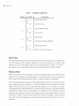
Bus Signal Lines
The bus consists of 16 signal lines as follows:
Table 1.
HP-IB Signal Lines
0101
Data Input/Output 1
•
•
•
•
•
•
0108
Data Input/Output 8
DAV
Data Valid
NRFD
Not Ready for Data
NDAC
Data Not Accepted
IFC
I nterface Clear
ATN
Attention
SRQ
Service Request
REN
Remote Enab Ie
EOI
End or Identify
The pin-outs on a standard HP-IB cable are shown below.
SHIELD
ATN
ATN
SAO
ground on
interface card
we
IFC
NDAC
NRFD
DAV
REN
DI08
Dl07
DI06
DI05
Figure 1.
HP-IB Cable Pinouts
General Information
Logic Levels
All signals use negative-true logic (low
log ical 1) •
High >2.4 V
Low <0.4 V
Line Termination
+5V
TKO
Each of the 16 bus signal lines is terminated as shown here.
HP-IB
6.2KO
851000
Line Drivers
Each of the signal Iines has a d river circuit with the following characteristics:
Type:
Open Collector
Output Voltage Low State:
<0.4 V@ 48 mA
Output Voltage High State:
>2.4 V @ -5.2 mA
Line Receivers
Each of the signal lines is received with a circuit having the following characteristics:
Hysteresis:
V t pos. - V t neg. ~0.4 V
Low State:
Negative Threshold voltage V t neg. ~0.6 V
High State:
Positive Threshold voltage 2.0 V ~V t pos.
Cable Length
A 4-meter cable is supplied with the card. Also see "Cable Length Restrictions" in Chapter 2.
Operating Temperature
Power Requirements
The calculator supplies all power for the card.
3
4
General Information
Bus Functions and Messages
The following table Iists the HP-IB functions and the capability available with the bus interface.
A complete description of these interface functions can be found in the IEEE Standard 4881975.
Table 2.
Bus Functions Available with the 98034A
Implementation
Function
SH1 (Source Handshake)
Complete Capability.
AH1 (Acceptor Handshake)
Complete Capability.
T5 (Talker)
Basic Talker.
Serial Poll.
Talk Only Mode.
Unaddress if my listen address (MLA).
L3 (Listener)
Basic Listener.
Listen Only Mode.
Unaddress if my talk address (MTA).
SR1 (Service Request)
Complete Capability.
RL.0 (Remote-Local)
Not Implemented.
PP2 (Parallel Poll)
Omits capability of being configured by controller.
DC1 (Device Clear)
Complete Capability.
DT0 (Device Trigger)
Not Implemented.
C1 ,2,3,4,5 (Controller)
System Controller.
Send Interface Clear (IFC ).
Send Remote Enable (REN).
Respond to Service Request (SRQ).
Send Interface Message.
Receive Control.
Pass Control.
Parallel Poll.
Take Control Synchronously.
General Information
The interface and calculator I/O ROMs determine how these functions are implemented to
generate messages for controlling the bus. Some functions are not available to the user with
certain calculator I/O ROMs. In many cases, the I/O ROM and interface handle the functions
automatically, as required, to simplify bus operation for the user.
Here is a complete list of bus messages and their corresponding bus command or line name
as described in previous HP-IB manuals. Refer to the appropriate I/O ROM manual for more
details.
Table 3.
HP-IB Messages
Message (command or line)
Description
Transfer instrument-dependent information between a talker
Data
and one or more listeners. It may be instrument programming information or data readings.
Trigger (GET)
Signals a group of selected devices to simultaneously initiate a set of device-dependent actions.
Causes an instrument to be initialized to a predefined or
Clear (DCL or SOL)
power-up state (a certain range, function, etc.)
Enables remote operation of all devices, allowing paramet-
Remote (REN)
ers and device characteristics to be programmed via data
messages.
Causes selected instruments to switch to local (front or rear
Local (GTL)
panel) control.
Prevents local (front or rear panel) control of instrument func-
Local Lockout (LLO)
tions.
Clear Lockout/Local (REN)
Removes all devices from Local Lockout mode and causes
all devices to revert to manual control. See the following
note.
Require Service (SRQ)
Indicates a device's need for interaction with the controller.
Status Byte
Transfers a byte (8 bits) of status information to a listener.
One bit indicates whether or not the device is currently sending the require service message. The other 7 bits (optional)
(Continued)
indicate device-dependent status.
5
6
General Information
Table 3.
HP-IB Message (cont.)
Description
Message (command or line)
Transfers a single bit of device-dependent status, which
Status Bit
may be logically combined with other Status Bit messages to
the controller.
Passes bus controller responsibilities from the current con-
Pass Control (TCT)
troller to a device which can assume the bus supervisory
role.
Abort (IFC)
Halts all bus operation and causes control to unconditionally
pass back to the system controller.
NOTE
When the 9825A Calculator is the system controller, pressing
8
automatically outputs the Abort and Clear
Lockout/Local messages.
Data Transfer Rate
The 98034A Interface transfers data at the rate of about 45k bytes (8-bit characters) per
second. The actual I/O rate can be considerably slower, however, and is determined by the
talker and listener(s) on line at any given time. The slowest device always determines the
actual data rate.
7
Chapter
2
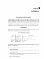
Installation
Unpacking and Inspection
If the shipping carton is damaged, ask that the carrier's agent be present when the interface is
unpacked. Inspect the interface for damage. If the interface is damaged or fails to meet
electrical specifications, immediately notify the carrier and the nearest HP sales and service
office (offices are listed at the back of this manual). Retain the shipping carton and padding
material for the carrier's inspection. The sales and service office will arrange for the repair or
replacement of your interface without waiting for the claim against the carrier to be settled.
Installation
Before plugging in the bus card, verify that its address and function switches are set to your
system's needs. The switches are preset at the factory as follows:
Table 4.
98034A Factory Settings
Factory Setting
Function
Switch
Select Code
7
A1S2
Parallel Poll Sense
Neg-True Logic (position 1)
A1S3 (1-5)
Calculator Address
Talk = U, Listen = 5 (off, on, off, on, off)
A1S3 (6)
System Controller
Enabled (on)
A2S1
Parallel Poll Bit
Bit 1
A1S1
Changing any of the switch settings except select code requires opening the interface case;
see page 10 for instructions.
After verifying (or changing) the switch settings, install the card as follows:
1. Switch the calculator off.
2.
Insert the bus card into anyone of the I/O slots at the back of the calculator. Press the
card firmly into the slot.
3.
Verify that the required I/O ROM is plugged in to provide the calculator with bus control;
see the manual furnished with the ROM.
4.
Switch the calculator back on.
8
Installation
Interconnecting Cables
A 4-meter cable is supplied with the bus card. The piggy-back connector end is connected to
the peripheral device. Other devices may be added to the bus by using the standard bus
cables listed below.
Length
Accessory Number
10631A
1 meter
2 meters
106318
4 meters
10631C
Figure 2.
Standard HP-IB Cables
Cabling Length Restrictions
In order to ensure proper operation of the bus, two rules must be observed regarding the total
length of bus cables when they are connected together:
•
The total length of cable permitted with one bus card must be less than or equal to two
meters times the number of devices connected together (the interface card is counted
as one device).
•
The total length of cable must not exceed 20 meters.
For example, there may be up to 4 meters of cable between the first two devices (2 devices x
2 m/device
= 4 m). Additional devices may be added using 2-meter cables up to a total of 10
devices (10 device x 2 m/device = 20 meters) using one 4-meter and eight 2-meter cables
(4 + (8 x 2) = 20). If more than ten devices are to be connected together, cables shorter
than two meters must be used between some of the devices. For example, 15 devices can be
connected together using one 4-meter and thirteen 1-meter cables (4
+ (13 x 1)
= 17).
Other combinations may be used as long as both requirements are met.
There are no restrictions to the ways cables may be connected together. However, it is
recommended that no more than 3 or 4 piggy-back connectors be stacked together on one
device. The resulting structure could exert great force on the connector mounting and cause
mechanical damage.
Installation
Metric Conversion Kit
The HP-IB cable furnished with the 98034A Interface is supplied with mounting fasteners
having metric threads. Other HP-IB instruments, however, may have either National Coarse
(American) threads or metric threads. The American-threaded fasteners are chromium plated,
while the metric-threaded fasteners are black.
Since metric and American threads cannot be connected together, a conversion kit can be
ordered. Use this kit to replace the mounting fasteners on any bus cable connector. Additional
conversion kits can be ordered by specifying HP Part Number 5060-0138.
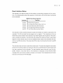
Select Code
The select code switch is accessible through a sma!1 hole on the top of the interface case. The
switch is preset to select code 7 at the factory. To change the setting, rotate the switch using a
small screwdriver.
Figure 3.
Select Code Switch
9
10
Installation
NOTE
When the 9825A Calculator is used, the bus card should not
be set to select code 0 or 1. Those codes are reserved for
internal calculator peripherals (display, keyboard, etc). Also
do not use the same code for more than one interface.
Interrupt Priority
Some calculator I/O ROMs enable a peripheral-interrupt scheme based on the interface select
code. Select codes 2 through 7 have a low-interrupt priority, while select codes 8 through 15
have a high-interrupt priority. If a device on the bus requires fast interrupt service, the interface should be set to a high-priority select code. See the appropriate I/O ROM manual for
more details.
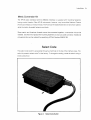
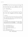
Removing the Interface Covers
Follow these steps to open the interface case:
1.
Switch the calculator off; then unplug the interface from both the calculator and the bus.
2.
Position the interface as shown in the first photo and remove only the four screws
shown. Then flip the interface over and remove only the upper-right and lower-left
screws.
3.
Carefully seperate the halves of the interface case and position them as shown in the
last photo.
To reassemble the interface:
1.
Be sure that all five pin connectors on one board are aligned with their sockets on the
other board.
2.
Position the cable wires so that they are not crimped as the case halves are pressed
together.
3.
Secure the cable-end of the case first, using the two long screws. Then replace the
other screws.
Installation
A. Remove only the four screws shown above.
c.
B. Flip the card over and remove these two screws.
Seperate the case halves and position them as shown.
Figure 4.
Opening the Interface Case
11
12
installation
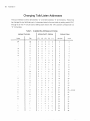
Changing Talk/Listen Addresses
The bus interface is set to talk address "U" and listen address "5" at the factory. These may
be changed to any talk/listen pair of characters listed in the next table by setting switch S3 (1
through 5) on the A 1 circuit board. Setting each slide to the "ON" position corresponds to a
"0" in the table.
Table 5.
Address Characters
Available Bus Addresses and Codes
Add ress Switch Settings
Listen
Talk
(5)
(4)
SP
@
0
A
Address Codes
(3)
(2)
(1 )
decimal
octal
0
0
0
0
0
0
0
0
0
0
1
B
0
0
0
#
C
0
0
0
$
0
0
0
%
E
0
0
&
F
0
0
G
H
0
0
1
0
0
I
0
0
0
J
0
0
K
0
0
1
L
0
0
M
0
0
N
0
0
0
+
1
0
2
2
1
1
3
3
0
0
4
4
0
1
5
5
0
6
6
1
1
7
7
0
0
8
10
1
9
11
0
10
12
1
11
13
0
12
14
1
13
15
0
14
16
1
1
1
15
17
0
P
0
0
0
0
16
20
1
0
0
0
0
1
17
21
0
18
22
19
23
0
20
24
21
25
22
26
2
R
0
0
3
S
0
0
4
T
0
0
5
U
0
0
6
V
0
7
W
0
8
9
1
0
1
1
23
27
X
0
0
0
24
30
y
0
0
1
25
31
Z
0
0
26
32
0
<
>
1
A
1
1
27
33
0
0
28
34
0
1
29
35
0
30
36
~
preset
Installation
Enabling System Controller
Switch S3(6) on the A 1 circuit board enables the calculator as the system controller. The
system controller function is enabled when A 1S3(6) is ON. Refer to the preceding photo.
Parallel Poll Switches
Switch S1 on the A2 circuit board determines which data bit is output in response to a parallel
poll operation. A2S1 is preset to bit 1 at the factory. To change the setting, rotate the switch
using a small screwdriver.
Switch S2 on the A 1 circuit board determines the logic level used when sending the parallel
poll bit. The switch is preset to use negative-true logic. To use positive-true logic, set A 1S2 to
the "0" position.
13
14
: nsta i latior
Notes
15
Chapter
3
Service
Introduction
This chapter contains a description of interface operation and instructions to help you repair
the interface. A complete circuit diagram and a list of replaceable parts are at the back of this
chapter.
Due to the microprocessor-based organization of this interface, it's recommended that the
interface not be repaired to the discrete component level. Instead, run the Functional Test
described next, and then the 98034A Test Procedure described in your calculator's System
Test Booklet. If either test indicates a defective interface, use the following Theory of Operation and Circuit Diagram to find the defective assembly.
If you have difficulty repairing the interface or if you would rather have HP repair it, contact the
nearest Sales and Service office for assistance; office locations are listed after the circuit
diagram.
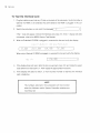
Functional Test
This test checks operation of most 98034A circuits. To perform a complete test of the interface, follow the 98034A Test Procedure in your calculator's System Test Booklet.
This test assumes that the interface switches are set to their factory settings:
98034A Factory Settings
Switch
Factory Setting
Function
A1S1
Select Code
7
A1S2
Parallel Poll Sense
Negative-True Logic (position 1)
A 1S3 (1 th ru 5)
Calculator Address
Talk = U,Listen = 5(off,on,off,on,off)
A1S3 (6)
System Controller
Enabled (on)
A2S1
Parallel Poll Bit
Bit 1 (least-significant bit)
Refer to Chapter 2 for instructions on setting the switches.
16
Service
To Test the Interface Card:
1.
Plug the interface card into any I/O slot on the back of the calculator. Verify that either a
General I/O ROM or an Extended I/O (with General I/O) ROM is plugged in the calculator.
2.
Switch the calculator on and verify the display. ('-_ _ _ _ _ _ _ _ _ _ _ _ ,]
If the i···· does not appear, remove the interface and press
B. If the
i···· display still does
not appear, refer to the 9825A System Test Booklet.
3. When an Extended I/O ROM is plugged in, execute this line and verify the display:
...
:: ..:::
...
=:::: :.. ~. ::
::.,::: .. :
:::.::::.=
When only a General I/O ROM is plugged in, execute this line and verify the display:
.0
••••
..
4.
.
.
,------::. .:_::: ._.:.::_ _ _ _ \J
If the display does not return after the line is executed, press
code switch to
5.
.
B
and rotate the select
a and back to 7. Then repeat the appropriate line above.
If the display still does not return, or if an incorrect number is returned, the interface
card is defective.
NOTE
The numbers returned in this procedure will be incorrect
when the Address and/or System Controller switches are
incorrectly set.
Service
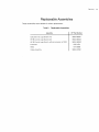
Replaceable Assemblies
These assemblies are available for direct replacement:
Table 6.
Replaceable Assemblies
Assembly
HP Part Number
Calculator I/O Logic Board (A 1)
98034-66501
HP-IB Control Logic Board (A2)
98034-66502
HP-IB Control Logic Board, without processor or ROM
98034-69502
Processor
1820-1691
ROM
1816-0868
Cable Assembly
98034-61601
17
18
Service
Notes
Service
Notes
19
20
Service
Notes
Service
Calculator I/O Lines
The data and control lines available at the calculator I/O slots are listed on the next page. The
lines are also shown in the block diagram on page 24. The bar above each line name indicates
that negative-true logic is used.
Table 7.
Calculator I/O Lines
Signal Direction
Description
Line
10D¢, thru 1007
~
interface)
Input/Output Data Lines
PA00 thru PA3
Peripheral Address Lines
'iCT thru
Register Code Lines
IC2
(Calc.
DOUT
Direction of Data Transfer (1
IOS8
I/O Strobe Line
FLG
Interface Flag (1
STS
Interface Status (1 = interface present)
INIT
Calculator Initialize (reset)
TRC
Interrupt Request Low (0-7)
=
output)
= interface ready)
IRH
Interrupt Request High (8-15)
INT
Demand Response to I nterru pt Poll
Bus Lines and Timing
The standard HP-IB signal lines are described next. The function of each line is fully described
by I EEE Standard 488-1975.
Data Lines (0101 -8)
The data lines are used to communicate all data including input, output and program codes,
addresses control, and status information between instruments connected to the bus. Data is
sent one character (byte) at a time (i.e., byte-serial and bit-parallel) under control of the
Transfer Lines. In most instruments, data is based on the 7-bit ASCII code. Unused data lines
terminate in a resistor load.
Control Lines (ATN, IFC, SRO, EOI, and REN)
The five control lines govern the flow of information over the data and transfer lines.
ATN (Attention) is driven by the active controller and indicates whether address commands
(ATN is low) or data (ATN is high) are being transmitted.
21
22
Service
IFC (Interface Clear) is used only by the system controller to initialize the bus via the Abort
message. When IFC is low for at least 100 /Ls, all talkers and listeners are stopped, the serial
poll mode is disabled, and control is returned to the system controller. When IFC is high, it has
no effect on the bus operation.
SRO (Service Request) is driven low by a device to indicate that it wants the attention of the
controller. SRO may be set low at any time except when IFC is low.
EOI (End or Identify) may be used to indicate the end of an instrument's character string.
When ATN is high, the addressed talker may indicate the end of its data by setting EOI low at
the same time that it places the last byte on the data lines.
REN (Remote Enable) is driven by the system controller and is one of the conditions for
operating instruments under remote control. Only instruments capable of remote operation
use REN and they monitor it at all times. Instruments that do not use REN terminate the line in a
resistor load. The system controller may change the state of REN at any time.
Transfer Lines (NRFD, NDAC, and DAV)
The three transfer (handshake) lines are used to execute the transfer of each byte of information on the data lines. All instruments use these lines and employ an interlocked "handshake"
technique to pass information. This allows asynchronous data transfer without timing restrictions being placed on any instrument connected to the bus. Transfer of each byte is accomplished at the speed of the slowest instrument.
NRFD (Not Ready for Data) indicates that all listeners are ready to accept information on the
data lines. When NRFD is low, one or more listeners are not ready for data.
NDAC (Not Data Accepted) is high to indicate the acceptance of information on the data lines
by all listeners. When NDAC is low, all listeners have not accepted the information.
DAV (Data Valid) indicates the validity of information on the data lines. When DAV is low, the
information on the data lines is valid for the listener(s). When DAV is high, the information on
the data lines is not valid.
Data Transfer
Transfer of data on the bus is asynchronous. It places no restrictions on the data rates of
instruments connected to the bus. The timing and levels required to transfer a byte of information on the data lines are shown in the next figure. Transfer is under the control of three
Service
lines:
DAV, NRFD and NDAC. The talker (sender of data) controls the data lines and DAV
(Data Valid) and the listeners (acceptors of data) controls both NRFD (Not Ready for Data)
and NDAC (Not Data Accepted).
The transfer of a byte of data is initiated by all listeners, signifying they are ready for data, by
setting NRFD high. When the talker recognizes t'JRFD is high and has placed valid data on the
data lines, it sets DAV low. When the listener senses that DAV is low and has finished using the
data, it sets NDAC high. Notice that the assertive, or action state, of both NRFD and NDAC is
high. Since all instruments on the bus have their corresponding lines connected together, all
listeners must be in a high state before that line goes high. This wired AND situation allows a
talker to recognize when the slowest listener has accepted a byte of data and is ready for the
next byte.
The next figure also shows the timing of the transition to the non-assertive· state of these lines.
A listener may set NRFD low when it recognizes that DAV has been set low; it must do so either
before or at the same time it puts NDAC high. The talker may return DAV to its high state after it
detects that NDAC is high. A listener may set NDAC low as soon as it recognizes that DAV is
high; it must do so either before or at the same time it places NRFD in its high state.
t_1---J r-t
0
r------------
- - - - - --I
DATA
- --
----
I
I
I
I
DAV
(TALKER)
NRFD
(LISTENER)
NDAC
(LISTENER)
-2
,
t
-1
0
.1
t
. 2
3
.4
(The curved lines indicate interlocked signal sequence.)
t
-2
Listene' b6corres ~eacy to accq:::t da:a
t
-1
Ta:~er
t
0
Irclca~es
has pu: data on the ines
data IS valid
'·e1~'es
t1
Listener has accepted tre da:a ar.::: ,:ocn;)e'
t
Talker indicates tile da:a 's no lonQer '.'alid an:::: T.a'.'
2
·3
Listener Indicates It is 'ead; for new cata
·4
A new cycle beginS (equivaent to t 0)
; -1
:c
t
0
Tille tha: data is put on ines before CAlis se:
Figure 5.
i: "e :::,2 :::
Cra~lge:
0/,
HP-IB Three-wire Handshake
23
24
Service
Theory of Operation
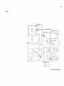
The 98034A interfaces the calculator to the HP-IB by performing four me
preting control bytes from the calculator, transferring data bytes from
HP-IB, transferring data bytes from the HP-IB to the calculator, and transfl
tion to the calculator.
A simplified block diagram of the interface is shown on the left. The
interconnections between processor, ROM, I/O registers and other circui
the processor, calculator 1/0 and HP-IB.
Calculator liO
HP-IB
The processor monitors the status of both the calculator I/O and the HP-II
I
~
...
I
I
....
Calculator
I/O
Registers
....L
...
I
I
I
I
Control Lines
......
I
I
I
-,
I
I
Bus
Address
Switch
.....
..
....
P'
......
Processor Data Bus '"\
the calculator command register. If this signal is true, the processor
r
....
Bus
Transceivers
....L
...
~{
Calculator
Interface
Interrupt
Logic
~
Data Input
Multiplexer
Multiplexer. If a condition is detected that requires action (for examph
...
quested .
.....
t
.
I
I
rp'
CFLG ......
I
Processor
and
ROM
Control
and
Interrupt
Logic
processor monitors the status of the HP-IB by periodically sampling it:
message) the processor issues the appropriate instructions to complE
-
CalculatorCommand
Register
is~
SRQ, REN, IFe and EOI) and its transfer lines (DAV, NRFD and NDAC
....
Select
Code
Switch
r
instructions to the other modules to decode and execute the requeste
Data:
DI01 - DI08
......
I
I
I
calculator is requesting an 1/0 operation by monitoring the CFLG (Calc
--..
Data Output
Latch
....
-,
.
...-
Transfer:
DAV
NRFD
NDAC
JControl:
IFC
ATN
SRQ
REN
EOI
r
Bus
Transceivers
....-,
--..
...
Please refer to the Complete Block Diagram on page 35 while reading
section.
Select Code Decoder and Switch
The function of the Select Code Decoder is to determine when the interf
the calculator. The interface responds only when the code on the perir
PA~ through PA3, matches the select code set on the select code switch.
Figure 6.
98034A Simplified Block Diagram
code enables the interface to look for an I/O command from the calculato
is ready for an 1/0 operation, the interface indicates its presence to the
the flag line (FLG) low and setting the status line (STS) low when no errc
the interface.
I(
Foldout
Theory of Operation
The 98034A interfaces the calculator to the HP-IB by performing four major functions:
inter-
preting control bytes from the calculator, transferring data bytes from the calculator to the
HP-IB, transferring data bytes from the HP-IB to the calculator, and transferring status information to the calculator.
A simplified block diagram of the interface is shown on the left. The diagram shows the
interconnections between processor, ROM, I/O registers and other circuits needed to support
the processor, calculator I/O and HP-IB.
The processor monitors the status of both the calculator I/O and the HP-IB. It determines if the
calculator is requesting an I/O operation by monitoring the CFLG (Calculator Flag) line from
the calculator command register. If this Signal is true, the processor issues the appropriate
instructions to the other modules to decode and execute the requested I/O operation. The
processor monitors the status of the HP-IB by periodically sampling its control lines (ATN,
SRO, REN, IFC and EOI) and its transfer lines (DAV, NRFD and NDAC) via the Data Input
Multiplexer. If a condition is detected that requires action (for example, a Require Service
message) the processor issues the appropriate instructions to complete the operation requested.
Please refer to the Complete Block Diagram on page 35 while reading the remainder of this
section.
Select Code Decoder and Switch
The function of the Select Code Decoder is to determine when the interface is addressed by
the calculator. The interface responds only when the code on the peripheral address lines,
PA¢ through PA3, matches the select code set on the select code switch. Receiving the preset
code enables the interface to look for an I/O command from the calculator. When the interface
is ready for an I/O operation, the interface indicates its presence to the calculator by setting
the flag line (FLG) low and setting the status line (STS) low when no error conditions exist on
the interface.
Service
110 Register Decoder and Calculator Command Register
The I/O Register Decoder is a network of gates which interprets the type of I/O operation being
requested by the calculator. It determines whether the transfer is an input or output operation
by looking at the DOUT line. For an output operation, the data on the calculator input/output
data lines (1000' through 1007) is latched into the Calculator Output Data Register when the
110 strobe pulse (lOS8) occurs. For an input operation when the calculator is not conducting
an interrupt poll (INT), the data in the Calculator Input Data Register is placed on the calculator data lines. For both input and output, the code on the DOUT, IC1 and IC2 lines is
latched into the Calculator Command Register when the I/O strobe pulse (lOS8) occurs.
The Calculator Command Register consists of a 4-bit latch and four open-collector NAND
gates. The latch holds the I/O register code (R4 through R7) determined by IC1 and IC2 and
the direction of the I/O transfer determined by DOUT. In addition, one bit of the latch is always
set when the calculator requests an I/O operation. This bit is buffered through one of the
NAND gates and becomes the Calculator Flag line (CFLG). Setting this line true causes the
flag line (FLG) to go high, indicating that the interface is busy. The other three NAND gates are
used to gate the DOUT, IC1 and IC2 signals onto the processor's data bus when it issues a
Read Calculator Command Register (RCCR) instruction. When the processor has executed
the requested I/O operation and is ready for another I/O operation, it issues a Clear Calculator
Command Register (CCCR) instruction, which clears the Calculator Command Register and
readies the interface for another I/O operation.
Calculator 110 Data Registers
The Calculator Output Data Register consists of two 4-bit latches and eight open-collector
NAND gates. As described earlier, this register holds the data to be transferred from the
calculator to the interface. The data contained in the latches is gated onto the processor data
bus when the processor issues a Read Calculator Output Data (RCOD) instruction.
The Calculator Input Data Register consists of two 4-bit latches and eight open-collector
NAND gates. The data on the processor data bus is latched into the two 4-bit latches when the
processor issues the Send Calculator Input Data (SCID) command. The data in this register is
transferred to the calculator input/output data lines when the calculator requests an input
operation.
25
26
Service
Calculator Interrupt Logic
The Calculator Interrupt Logic allows the interface to request service from the calculator for
several conditions which are described later in the section "Controlling the Interface". The
Calculator Interrupt Logic is a network of gates and a one-of-eight decoder. This logic pulls
the appropriate interrupt request line (IRL or IRH) low when the processor issues a Calculator
Interrupt Request (CIRQ) instruction and the calculator is not conducting an interrupt poll
(INT). IRL is pulled low when the select code switch is set to an address between 0 and 7, and
IRH is pulled low when the switch is set between 8 and 15. When the calculator senses a
service request, it conducts an interrupt poll to determine which interface requires service. A
poll is conducted when INT is low. When the most-significant bit of the peripheral address
(PA3) matches the most-significant address bit from the Select Code switch, the Calculator
Interrupt Logic pulls one of the calculator input/output data lines low. The setting of the Select
Code switch determines which line is pulled low, as shown in the following table:
Interrupt Request Bits
Select Code
Line Pulled Low
Oor8
100¢
1or9
1001
2 or 10
1002
3 or 11
1003
4 or 12
1004
5 or 13
1005
6 or 14
1006
7 or 15
1007
Control Logic
The Processor, ROM I/O Register Selector, and Oscillator form the control logic portion of this
interface. The Processor controls all interface operations by issuing instructions via seven
control lines, the 8-bit processor data bus, and selecting I/O registers via the I/O Register
Selector. The algorithms for interface control and the implementation of the HP-IB interface
functions are contained in the 4096-bit ROM. The Oscillator generates a 2 mHz (approx.)
asymmetrical waveform which is used as the main clock for the Processor and as the enable
signal for the I/O Register Selector.
The Processor also contains a vectored interrupt structure for conditions that require immediate action. These conditions are described next.
Service
Processor Interrupt Logic
The Processor Interrupt Logic is a network of gates that provides the ability to interrupt the
processor for either of two conditions:
•
When an Abort message (IFC) is received from the HP-IB or
•
When the control line ATN is set true by the controller in charge.
An interrupt occurs for the second condition only when the calculator is not the active controller.
The processor enables the interrupt logic via the Interrupt Enable (lENA) line. When' an Abort
message is received via the HP-IB, the interrupt causes the processor to generate a 100 JLs
pulse on the IFC line and then initializes all of the HP-IB interface functions within the interface.
The IFC line was previously set true as the result of an I/O operation from the calculator.
When the interface is not the active controller, the processor not only enables the interrupt
logic via the Interrupt Enable line, but also sets the Immediate Control line (IMD) true. When an
Abort message is received, the interrupt logic generates a vectored interrupt to the algorithm
which initializes all of the HP-IB interface functions. In addition, when the controller in charge
of the HP-IB sets the ATN line true, the interrupt logic immediately clears the HP-IB Output
Data Latch and disables the HP-IB Transceivers for the HP-IB data lines (0101 through 0108),
the DAV line, the NRFD line, and the EOI line; then the NDAC line is set low. This leaves the
interface ready to receive data from the controller. A vectored interrupt is also generated to
the algorithm which controls the acceptance and analysis of the data sent by the controller.
HP-IB Output Data and Control Bus Latches
The HP-IB Output Data Latch consists of two 4-bit latches. Data is transferred from the
processor data bus into this 8-bit latch when the processor issues the Send Interface Bus Data
(SIBD) command. The outputs of this latch are routed to the HP-IB data lines via the drivers
contained in the HP-IB Tranceivers.
The HP-IB Control Bus Latch is a 5-bit latch which holds the bit pattern to be applied to the
HP-IB control lines (EOI, ATN, SRQ, REN and IFC). The appropriate bit pattern is transferred
from the processor data bus into this latch when the processor issues the Send Interface Bus
Control (SIBC) command. This latch consists of one 4-bit latch and one 0 flip-flop. The outputs
of this latch are routed to the bus drivers contained in the HP-IB Transceivers.
HP-IB Address Register
The HP-IB Address Register consists of a hex, tri-state buffer and six switches. Five of the
switches are used to set the five least-significant bits of the HP-IB talk/listen address. When
each switch is off, its corresponding bit is set to a logical 1. The HP-IB address switches are
27
28
Service
connected to the five least-significant bits of the processor data bus (DO through 04). In
addition to the HP-IB address switches, this module also contains the System Controller
switch. When this switch is on, the interface assumes the role of system controller. This switch
is connected to bit 05 of the processor data bus. The contents of this register is gated onto the
processor data bus when the processor issues a Read Interface Bus Address (RIBA) instruction.
Data Input Multiplexer
The function of the Data Input Multiplexer is to route either a data byte (0101 through 0108) or
a control byte (EOI, ATN, SRO, REN, IFC, OAV, NRFO and NOAC) from the HP-IB Transceivers
to the processor data bus. The processor selects the data byte by issuing the Read Interface
Bus Data (RIBO) command. The control byte is selected when the processor issues the Read
Interface Bus Control (RIBC) command.
This module consists of one AND gate and two, quad 2-to-1 multiplexers.
HP-IB Transceivers
The interface uses four bus transceiver modules. Two are used for the HP-IB data lines (0101
through 0108) and two are used for the HP-IB control lines (EOI, ATN, SRO, REN, IFC, OAV,
NRFO and NOOC). These transceivers allow bidirectional flow of data and control information
between the interface and the HP-IB. Each transceiver provides four open-collector drivers
and four receivers with hysteresis.
Parallel Poll Logic
The Parallel Poll Logic provides the capability to respond to a parallel poll conducted by the
controller in charge of the HP-IB. When the controller initiates a parallel poll (A TN and EOI
true) and the calculator has requested service from the controller via the SRO line, the parallel
poll logic sends one bit of status to the controller via one data line (0101 through 0108).
This logic consists of a 3-input NAND gate, a slide switch to set the logic level of the bit, and a
switch to select which bit on the HP-IB data lines will be used to send the response to the
parallel poll.
Initialize Circuit
The Initialize Circuit applies +9 V to the processor after all other power supplies are stable.
This condition is indicated by the initialize signal (INIT) from the calculator, and causes the
processor to execute an initialize algorithm. If the interface is the system controller, this
algorithm issues the Abort message (IFC) and sets the REN line true. If the interface is not the
system controller, this algorithm clears all HP-IB interface functions. This circuit also provides
a reset pulse to the HP-IB Control Bus Latch.
Service
Controlling the Interface
The calculator controls the interface via four I/O registers, R4 through R7. These registers are
memory locations used for the storage of input and output data. It should be noted that these
four registers are not dedicated components on the bus interface. Instead, all data passes
through the Calculator I/O Registers (see block diagram on page 24) and is temporarily stored
in the processor's read/write memory. A store operation from the calculator to anyone of these
registers transfers the data to the interface previously selected by the peripheral address. A
load operation from any of these registers into the calculator transfers the data from the
selected interface to the calculator.
The calculator I/O signals IC1 and IC2 determine which I/O register is addressed, as shown
below:
IC2
IC1
a
a
a
R7
1
R6
a
R5
Register
R4
The contents of each I/O register are assigned unique roles such as data, status or control
(see the next table). These assignments are described in the following pages.
NOTE
The calculator's store and load instructions mentioned here
are internal routines, used by I/O ROM to implement the
user-language I/O statements and functions. Registers R4
through R7 are not intended to be directly accessible via
user-language operations.
29
30
Service
Table B.
Register
R4
R5
R6
Direction
{
{
IN
OUT
IN
I/O Instruction
Request Data from Bus
Send Data to Bus
Interface Status Request
OUT
I nterrupt Byte
{
IN
Null Operation
{
IN
OUT
R7
I/O Register Assignments
OUT
Send Multiline Interface Message
Get Parallel Poll Byte
Send Uniline Interface Message
Send Data
The least-significant eight bits of data contained in the calculator accumulator is transferred to
the HP-IB data bus (0101 through 0108) when a Store R4 instruction is executed. Data
transfer occurs only if the interface has previously been addressed as a talker on the HP-IB. If
the interface has not been addressed to talk, the calculator status line (STS) is cleared.
Receive Data
When a Load R4 instruction is executed, the interface accepts a data byte from the HP-IB and
places it in the Calculator Input Data Register. If the interface has not been addressed to
listen, however, the calculator status line (STS) is cleared and data is not accepted.
The first Load R4 instruction received by the interface after any other I/O instruction is essentially a request data byte instruction. The data byte placed in the Calculator Input Data
Register may be transferred into the least-significant eight bits of the calculator accumulator
by executing either a Load R6 instruction or another Load R4 instruction. In this case, both the
Load R6 and Load R4 instructions are treated as "no operations" by the interface. The Load
R6 causes the interface to remain in the input-data routine, permitting successive Load R4
instructions to rapidly input data. Two Load R4 instructions are needed to input each data
byte; the first Load R4 requests the byte and the second Load R4 transfers the byte to the
calculator.
Service
Read Interface Status
The calculator can read the status of this interface by executing a sequence of five instructions. The following table shows the sequence of instructions and the information transferred
to the calculator:
98034A Read Status Sequence
Instruction
Data Byte
Load R5
HP-IB Interface Signature
Load R6
First Status Byte (Device Clear and Error)
Load R6
Second Status Byte (HP-IB Address)
Load R6
Third Status Byte (HP-IB Control Byte)
Load R6
Fourth Status Byte (Interface Status)
The execution of the Load R5 instruction causes the interface to transfer a data byte to the
calculator. The fifth and sixth bits are always set to a logical 1. The remaining six bits are
determined by the contents of the Calculator Input Data Register and are ignored. This byte is
used to identify the interface. This instruction also causes the interface to enter a read status
algorithm, which transfers each of the four additional status bytes to the calculator with successive Load R6 instructions. If the status line (STS) is clear, it will be set by the fourth Load R6
instruction.
The calculator does not have to read all four status bytes. The read status algorithm terminates
whenever the interface detects an instruction other than Load R6 before the fourth status byte
has been transferred to the calculator. The read interface status instruction must be completed, however, in less than 100 ms. This restriction is necessary to insure that the Abort
message (IFC), sent by the controller in charge, is not missed. The bit assignments of the four
bytes are summarized on the next page.
31
32
Service
First Status Byte:
¢
91
Bit 0:
Is 1 when error detected.
Bit 2:
Is 1 when Device Clear received.
Device
¢
¢
¢
~
2
3
4
~
§
Z
Clear
}t
Error
Second Status Byte:
6
7
4
5
3
0
(MSB)
0
2
Hr-1B Addre~s
(LSB)
Third Status Byte:
7
6
5
4
3
2
EOI
REN
SRQ
ATN
IFC
NDAC
0
NRFD
DAV
Serial
Poll
Set
0
End
of
Record
Logical 1 indicates corresponding signal line is true.
Fourth Status Byte:
7
6
5
4
3
System
Controller
Set
Service
Controller
Talker
Listener
Request
Active
Active
Active
Bit 7:
Is 1 when the SRQ signal line is true.
Bit 6:
Is 1 when the calculator is the active controller.
Bit 5:
Is 1 when the calculator is the active talker.
Bit 4:
Is 1 when the calculator is an active listener.
Bit 3:
Is 1 when the calculator is the active system controller.
Bit 2:
Is always 1.
Bit 1:
Is 1 when a serial poll is in process.
Bit 0:
Is 1 when the EOI (end of record) line is true.
Figure 7.
2
1
Interface Status Bytes
Service
Interrupt Operation
The 98034A can be enabled to interrupt the calculator by transferring an interrupt-enable byte
from the calculator accumulator to the interface with a Store R5 instruction. The bit assignments in the interrupt enable byte are shown in the following table:
7
6
5
4
3
2
Input
Register
Full
Output
Register
Empty
Service
Controller
Talker
Listener
Request
Active
Active
Active
Bit 7:
Logical 1 enables interrupt on SRQ.
Bit 6:
Logical 1 enables interrupt on active controller.
Bit 5:
Logical 1 enables interrupt on active talker.
Bit 4:
Logical 1 enables interrupt on active listener.
Bit 3:
Logical 1 enables interrupt on input register full.
Bit 2:
Logical 1 enables interrupt on output register empty.
o
Other
Interrupt
Conditions
Enable
EOI
Bit 1: Logical 1 enables interrupt when error detected, device clear or selective device
clear/received (when not active controller), or EOI received.
Bit 0:
Enable EOI to clear status line (STS).
Figure 8.
Interrupt Enable Byte
When the interface receives a Store R5 instruction, the interrupt enable byte is transferred
from the Calculator Output Data Register to an internal read/write register in the processor.
The interrupt enable algorithm then checks the byte against existing conditions to determine if
an immediate interrupt should be generated. Any of the following conditions cause an immediate interrupt:
•
SRQ (service request) detected.
•
Interface is active controller.
•
Interface is active talker.
•
Interface is active listener.
•
Output register empty.
The calculator status line (STS) is cleared when the interface generates an interrupt for any of
the above five conditions. The status line is only cleared on the first output-register-empty
interrupt. All subsequent output-register-empty interrupts will have status set.
The interrupt request from the interface (IRL or IRH) can only be cleared by executing a Load
R6 instruction. If the status line has been cleared as the result of an interrupt, it can be set by
reading the interface status.
33
34
Service
Sending Interface Messages
When a Store R6 instruction is executed, the eight least-significant bits of the data contained
in the calculator are transferred to the Calculator Output Data Register on the interface. The
interface interprets this instruction as a command to send a multiline interface message to
other devices on the HP-IB. If the interface is the active controller, the ATN line on the HP-IB is
then set true and the byte in the Calculator Output Data Register is transferred to the HP-IB.
After this multiline message has been transferred, the ATN line remains true until either an
instruction other than Store R6 is received by the interface or a Pass Control message (TCT) is
transferred to another device on the HP-IB with a Store R6 instruction. When the calculator is
not the active controller when the Store R6 instruction is received, the interface clears the
status line (STS) to indicate an error.
The interface sends uniline interface messages to other devices on the HP-IB when the
calculator executes a Store R7 instruction. If the byte received via a Store R7 instruction has
the eighth bit set to a logical 1, the remaining bits in the byte are sent as uniline messages, as
shown in the following diagram:
7
6
5
(not
~Sed)
4
3
2
EOI
IFe
ATN
o
REN
SRQ
Request Service
When the eighth bit of the byte received with a Store R7 instruction is set to a logical 0, the
instruction is interpreted as a Require Service message. The seven least-significant bits of this
byte are stored in one of the processor's read/write registers. This byte is transferred to the
controller in charge when a serial poll is conducted. If the seventh bit of the byte is a logical 1,
the interface automatically sets the SRQ line true and requests service from the controller in
charge.
Parallel Poll
The calculator can conduct a parallel poll when it is the controller in charge. A parallel poll is
initiated by setting both the ATN and EOI lines true. The calculator can accomplish this by
executing a Store R7 instruction with the appropriate byte, as described in the Send Interface
Messages section. Once a parallel poll has been initiated, the Status Bit message on the
HP-IB must be transferred to the Calculator Input Data Register. This occurs when the calculator executes a Load R7 instruction. The byte that represents the parallel poll response is
then transferred to the calculator with a Load R6. The parallel poll is terminated when the
calculator executes a Store R7 instruction with the appropriate byte to clear the ATN and EOI
lines.
Service
Notes
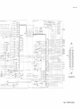
~CALCULATOR
14-------.....
~,o/..!,!00CJL----po--------------~~:_..,r+I.lll~~r;;~;~O:T~1E--Rc.:C"-'O"'O'---____
c-----'--
~
-l
~
4
f-----2---
f-----L--
~
~
SELECT
~~~~C H
,-
CALCULATOR
IRN:~I~~t~A
14--~""TIi------+--~-----"':;:~~;:':;;::":;;;;;';';;'~~~;;';;'-~r---+l
PROCESSOR DATA BUS (8 LINES)
1E__.......<.LlL-----
1-..
HP-IB
OUTPUT
DATA
LATCH
~
I/O REGISTER SELECT LINES (9)
(4 LINES)
....--;..-01
I RIB'"
v----'
lL------'
1E---41r---~
h-:--;;
-
I
SIBD
HP-IB
"'OORESS
010 I
(8 LINES)
H P-I B
TRANSCEIVERS 1--_.".5_--1
6
I
REGISTER
(SWITCH)
010 8
;
SELECT
OIOt - 0108
CODE
DECODER
PARALLEL
:~~~C ~ ~
REOI
++_____---j INTERRUPT
L _ _ _ _ _ _---1_ _ _ _ _ _ _
(SWITCH)
~----
C"'LCULATOR ....- - I - - - - ' . ! : I R ! ! , L - - < E - - - - - - - + - - - - - - - I - t - - - - - - 1 L O G I C
IRH
~~~II~LlZE
DECODE
,,~
'n
~
~--'-----.~I-+--------t_t_\l
~-I-
HP-I B
L------'T:'~r--------.
I
H P-IB
I---=-N"'RF'-D~-I
TRANSCEIVE"I--=E",OI~---1
RESET
f----
~~~-------_r~~__~__~~~~S~T~O~RE~I~~R~E~G~IS~TE~R~ID~'l
r---+-
INPUT
~
fI/O REGISTER
HP-IB
MULTIPLEXER
"'"'' U""
---I_t--____~
I--l!'iNII.!IT_ _ _ _ _ _ _+ +_ _ _ _ _ _
(8 LINES)
1..-+--,-,1M"'O'--_ _-i
INTERRUPT
LOGIC
1+---1
NDAC
-1_~C~L~EA~R~HP~-~IB~_~~I---
'---------"
I
(4 LI NES)
~
IAn
HP-IB
CONTROL
BUS
LATCH
I-'£IRl>!S"'-Q_ _--I HP-IB
ATN
SRQ
I-'£IR",E!J..H_ _ _-tiTRANSCEIVER I-""RE""N'-----1
liFe
IFe
~~------------------------------~-----------------I~~====~I
VO REGISTER
SELECTOR
I.....-
J'
I
PROCESSOR L-....a,r-- L - -
r-- ..
ROM
I OSCILLATORI
Figure 9.
98034A Detailed Block Diagram
35
36
Service
Interface Ass emblies
98034 - 66501
5040~
/
5040-7804
I
I
98034-66502
5040 -7801
5040 -7803
s
i/---------~
\~
98034-61601
.,
Service
Table 9.
REFERENCE
DESIGNATOR
A1
A1C1,C2
A1C3
A1C4,C5,C6
A1P1-P5
A1Q1
A1R1
A1R2-R5,R8
A1R6
A1 R7
A1SW1
A1SW2
A1SW3
A1U1
A 1 U2,U6-U8,
U11,U16,U18
A1U3,U4,
U12,U13
A1U5
A1U9
A1U10
A1U14
A1U15
A1U17
A1U19
A2
A2C1,C2
A2C3,C6,
C8-C10
A2C4
A2C5
A2C7
A2C11
A2CR1
A2CR2,CR3,
CR5
A2CR4
A2P1-P5
A2J1
A2Q1
A2R1
A2R2
A2R3
A2R4,R9,R12
A2R5
A2R6
A2R7
A2R8
A2R10
A2R11
A2R13
A2SW1
A2U1
A2U2
A2U3
A2U4,U5,U11
A2U6
A2U7
A2U8
A2U9,U10
A2U12
A2U13
A2U14-U17
W1
I
I
-bPPART NO.
Replaceable Parts
DESCRIPTION
TO
98034-66501
0160-3847
0180-0106
0160-3622
1251-4257
1854-0019
0683-5625
0683-2225
0683-1025
0683-4725
3101-2097
3101-1341
3100-3364
1820-1297
1
2
1
3
5
1
1
5
1
1
1
1
1
1
PC Assembly, Calculator I/O Logic.
Cap, Fixed: 0.Q1I£F,100V.
Cap, Fixed: 6OI£F,6V.
Cap, Fixed: 0.1I£F,100V.
Plug: 6 pin.
Transistor: NPN,Si.
Res, Fixed: 5.6Kn, 5%, 1/4W.
Res, Fixed: 2,2KO, 5%, 1/4W.
Res, Fixed: 1Kn, 5%, 1/4W.
Res, Fixed: 4.7Kn, 5%, 1/4W.
Switch,4PDT: Select Code.
Switch, 1PDT: Parallel Poll Sense.
Switch, 6 Gang: Address & System Controller.
IC: 74LS266, Quad NOR Gate.
1820-1198
7
IC:
1820-1562
1820-1199
1820-1284
1820-1427
1820-1144
1820-1195
1820-1203
1820-1266
98034-66502
98034-69502
0180-0210
4
1
1
1
1
1
1
1
1
2
IC: MM74C175N, 4-bit Register.
IC: 74LS04A, Hex Inverter.
IC: SN74LS55.
IC: SN74LS56, Decoder.
IC: SN74LS02N, Quad NOR Gate.
IC: 74S175, 4-bit Register.
IC: SN74LS11N, 3-input AND Gate.
IC: MM80C97N.
PC Assembly: HP-IB Control Logic.
PC Assembly without U1 and U2.
Cap, Fixed: 3.3I£F, 15V.
0160-3622
0160-3334
0180-0106
0160-3847
0160-3482
1906-0075
5
1
1
1
1
1
Cap, Fixed:
Cap, Fixed:
Cap, Fixed:
Cap. Fixed:
Cap, Fixed:
Diode Array.
1901-0040
1902-3018
1251-4215
1251-4333
1853-0016
1810-0264
0683-5615
0683-3325
0683-2225
0683-1815
0683-2025
0683-5625
0698-3225
0698-3557
0683-1035
3100-3378
1816-0868
1820-1691
1820-1216
1820-1562
1820-1753
1820-1201
1820-1199
1820-1439
1820-1417
1820-1425
1820-1689
3
1
5
1
1
1
1
1
3
1
1
1
1
1
1
1
1
1
1
1
3
1
1
1
2
1
1
1
Diode: Si, 0.05A, 30V.
Diode: Zener.
Connector: 6 pin.
Connector: 24 pin.
Transistor: PNP,Si.
Resistor Network.
Res, Fixed: 560n, 5%, 1/4W.
Res, Fixed: 3.3Kn, 5%, 1/4W.
Res, Fixed: 2.2Kn, 5%, 1/4W.
(Optimum value selected at the factory)
Res, Fixed: 1.8Kn, 5%, 1/4W.
Res, Fixed: 2Kn, 5%, 1/4W.
Res, Fixed: 5.6Kn, 5%, 1/4W.
Res, Fixed: 1430n, 1 %, 1/8W.
Res, Fixed: 806n, 1 %, 1/8W.
Res, Fixed: 10Kn, 5%, 1/4W.
Switch, 1P1 OT: Parallel Poll Bit.
IC: PROM.
IC: Nanoprocessor.
IC: SN74LS138N
IC: MM74C175N, 4-bit Register.
IC: MM74C74N
IC: SN74LS08N
IC: 74LS04N, Hex Inverter.
IC: SN74LS258N
IC: 74LS26N
IC: SN74LS132N
IC: MC3446P
98034-61601
1
Cable Assembly.
5040-7801
5040-7802
5040-7803
5040-7804
2200-0510
2200-0536
5040-7836
7120-5166
7120-5167
98034-90000
1
1
1
1
2
8
1
1
1
1
Cover, Plastic: Left Front Housing
Cover, Plastic: Right Front Housing.
Cover, Plastic: Left Rear Housing.
Cover, Plastic: Right Rear Housing.
Screws: 4-40, long.
Screws: 4-40, short.
Latch: Plastic.
Label: Front Housing.
Label: Rear Housing.
Manual: Installation and Service.
*
SN74LS03N, Quad NAND Gate.
0.1I£F, 100V.
0.01I£F,50V.
6OI£F,6V.
0.01I£F,25V.
430 PF, 300V, 1 %.
I
37
38
Service
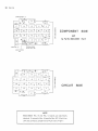
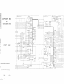
parallel poll logic (1)
PI
c:::==J
6
1
-RI-
...........
~
0
CO
::J
COMPONENT
()
CO
A1
()
0
c
SIDE
-hp- Part No. 98034-66501
RevS
SW5
talk/listen address
(off, on, off, on, off)
select code (7)
system controller
(on)
6.- - -
,---, r- - - - -;
,
C'S I
SWI
:
, L ___ J
---,1
'--p-z--'
---C3---
1:- - --; Ir
- - -
I
UI3
I,
ua I '
L _ _ _ _ -19 '- _ _ _ Ja ~
-1
U4
I
___ ~~
I
I,---,Ir---l
I
UI9
I lUIS
,
L ____ '9 L ___ J8
I, I
- -I
Ul8
I
L ___ ...1a
11----,
I
UI7
Ir - I
~
-- R6--
____
J9
1,----,
I
L ___ Ja
-- R7--
- -,
UI5
I
I
UI4
I.,JQI
I
L ___ Ja
..,
,-=~W~=:
--R2 - 1,- - - - . , 11- - - - . , I r - - ,
UI2
I,
U7
"
U3
,
'9 '
I
I
L_ -
-
-
-'
UII
-
-
J8 '-- -
1,---'
Ir---:
,
'- -
iL
I
L _ _ _ J8
U6
:
_ _ _ Ja
I,---llr---l
,
UIO
I
L ___ ...J9
1,---,
:
I
I
U9
C,5
:
U5
'- _ _ _
:
I
-'C2
I
I
, ,
- - 9C~
1.----': 1
:
U2
:1
L _ _ _ JEl'
Ir---,
..Ja
:
UI
...........
"-
o
co
::J
()
co()
o
C
CIRCUIT
:
'- ___ .J8
--RI--
6=-=-_-_-.:;1
L ___ Ja' ,..------P-I---'"
P4
NOTE
98034-66501 Rev. B and Rev. C boards are electrically
identical. To convert a Rev. A board to Rev. BIC, lift pin 5 on
U 14 and connect a jumper from U 14 pin 5 to U 14 pin 7.
SIDE
~Q~4--~L~J:ATORI/Ol..;G~C----------------
COMPONENT
SIDE
---<I (
+5V
""----<l (
A2
-CR2-
-R2-c.-C2-
A L, L L L L L
-hp- Part No. 98034-66502
Rev B
-CR3-
-R3-R4-
:::~~:
I
,,"
~:8: ~
.,i" ,,"
II +5V~,
~
,..u.,
+5V
.,
+5 V
+"V---<'8~
~
~--<16
)~
'--~"
J
PiIT--<'4
~
1
PA0--<13
"
'R4-
I
R3 -_C¢k3 _-:
U'.
'
Ule
4
3-c:(U6.1.
,~
I':
"
I·
'
I
1
5:--- 1;
_--<'I
CIRCUIT
SIDE
:1
"-
,~.
:~
'~o'
,,-"
~
103Q
5
UI2
! L----t-+++++-------""~,
I
,
I
~~"
'----
D4
SWITCH
z0r-~
i
I
_
R:r
$IUI8C
.,
___
~
_______
~
,
in ohms and capacitor values are shown in
I
ffi---(N
9S.
mli---(_E
:olor indicates the narrower strip (e.g., 924
6
7
Blue
Violet
8
9
Grey
White
voltage in the range of -2 thru -5 volts.
3Kf! (-5V).
G
II
rENA
12
I
29
IR
:~
[C)
50 1E I..tA)
CCCR
J3
I~
I
~U7e
j""_ _++_---"'---¥"---..!..
.1'--'-----"l"''''
,~'"
~
L_-_-_ _ _
10
----'7l
)>-.cc~'----""'------+-<':'q
~~)
I
UI4c 9
C5
60
i
CIRQ
i
B~
·V.....
~5io-oe-- - - - - - - - - - - - - - - - - - - - - - - - - - - - - - - - - - - - - - - - - - - - - - - - - - - - - - - - - - -
~
I
F8'"' ".
UI3c
S
'I:
UTe
E
~:
R/W
+5V
r~16
CR'
I
'''''
O
+5V
'"1'-------'''
P"6~ As
PI7~ .11
-&
),)
----------i
I.~~,m.'~~~~
mIT
6.6
.O~
K
""f'!--------!'~,~
::~::
::~ ::~
::::::::
ClO
'
.. 1 . 1
Jl
I
l
III
'Ii
:1.1
:::~+5V
BAa
~+l2E~K.
"~~~~~
V
::
!
4ilF""t-I-----,
U4
12
D6
07
30 U5 30 II
"" :" ,,"
,.~
:,~
fJrh]l
I:
+-5'(
!
04
'--1-+++-t--t-----t-+--_t-t-+-j-
t--t---
t-I
CONTROL'U'L4TCH
,,~-
,
:".rr:'-,t_-tt--_-_-_-_-~+-t-=H-'-+t---t--H---hl-----t-
LI----~~,-Tii2.:2K2K
"'f'-----'"
,j.T(C~ ~I
t C8 i
~
01
d:<c--/------------+-"I:::~
:
1
~~~I
-+--,
1
J
'---+---H-+-+-
-~.-~----~----~---~~~~~-~~-~~~
,~ rr~E----"IT-'ALlZE-'OGIC--+-"1"'"
U2: .. H
~
..
1
--.--~----+------t----_t_t-~:--.~~---t----t-~H-
+5V
leo
I
""'~,
U8,
.
I
1 I i Jr-;:~~::;~=~~=
III!
,,"
~t'-
1
T.1
PI
6)
~
. (~
.
JI
""
,
'------~ : l ! = :--'
"--_____-t__________
--_----i- ~
"'F'_t_t-~--rT-_t_T-c-:--t-_t_HH-T-~
UID 3e!0
,,"
1"45K
-->,)>--;-,--~""----'----«,f----
"'r'++_--++-+t-lr-t++-H--t-+-
2A S
::I":.'---++----"'---P"'----"'" ;,::
p.o,]_ _
+5V
."' ~H~'
OEOCQER
10.",:,
r--t:!i-'t-:;t'-t-I+-----+~"O(U'4
" ' U'4> :
r-t-
'----...:.·-+---+--1~-~-~----+-I'=====~
I
:
""si"'''-t---+t--H-+-++-t-+-++H-+-+-+-
041""'---++----"'''---1
106
::~~+5V
lL
10
C
~~y
t---
--t----t-t----r-t-i
'--r 2:~/5Vr----'
Du,.,):::
D3~
C~'
~~
'i~,~
L--·-l-----------~~_+---------7'
~30Pf
L-f--.!!
CALCULATOR !N"R'UPT "OG
,.'
"'r"~-_t__+---~~-t"~~-'i' "
" "'"
SE~::C70P
~"
I
iRH---(IIf--------------------------~U28
The first number indicates the base color,
~
~):>:'+-----"'D''iI
UI5
~
~'"
flJ--'"
"
'~i~~-~
5
~~-----------~'~U=2'~,+-;~~~~~~~~~~~~~~~~~~~=~~.:I~==~==~=:~~:~=~-~-,-U~5-.~~~.f~~~~~~~~~~~~~~~~~~~~~~~~~~~~~~~~~~~~~.!
fRi:---(t2
UI3c
UI38
4,....
I
~/O-.''+'_ _ _~DI..
: '
'" ".><
..
"I
~.
1i
L-----+''C.:~. ~
~
UI3A:3
IIO REGISTER
:,15
,
1
~
'I
2", I
~¥!"
,," t----2L
"",,,.,,, ~
i-L
' " ,
,,~
~+5V
f~~
"'----"~,,
IREQ
:::~-"',~~,-,-~-;U-,60-,---I------+-------71)>-'-~---"""'~~--«11, :~
!
r.=jF:·
t~r· "
6
4-H-,'
lLJ,,~,r-t-:
"I
I
..
I
~~: f-t-----+---1-+++-H------+:-t--++H-t----4::
I:
2
Ii
!
0'
"'f'-t---_t_t--MH-t--t-t-,
p'''-----------+'''-t~ ,~ U9 ::.e,"""-t---_t_t--H_t__t_-t-If---IA.CK·
':3Ar'''-t---_t_t--H_t_-;
I
~C:OISNTTER:O~LLE"R?
rU~'
=h
: _
I
5 UI2e
n
z
i
~~~CT
tL,~
~U8
•
:--.
"t'-r--2?
.~
MU~r:--r--___t_r--~_t__t__+1-~
"I
~
(:
DATA NPUT
:2
3
REO'
' \ PROCESSOR DATA BUS
I
I..:
•• , : )
¢
I
2~K
D5UT--<T
I
'(f~
6
L I - -_ _ ~------------~)6)~--~~--~~I~~'--'
I~I
I
1
~1):
"~~~~I
I.
6;---::;N--~6~'J; 1 oo<Uf]"
';'
f;"UI7,:,
~-~I..I....i..............::......,\i,\..........................
(5
( ~
J,3 (6
IMO
:,.
'I
-'
~I
,.
R1
t5V--"";c..o...I------__--,t)2),..:'''"-'_ _-""R'..,BA'--_ _ _''''-<C,'-____---I--'l'rr "
'~'--~_~--~-u~I------------~'4~---~K~~----~,
. Y5 W,I'-._ _ _-"j!~"DS3.rENABLE INPUT DATA
7 .
,4;
"..::::1
I
: CR. :
,
~~
'N
I
I
!
I
-
~----'
o.:~:
m--<~,O~~---~~~~~~~~~~-~~:-U-I7-'-'~~~II~I~~~~~~~~~~~~U~D~.~w~.~U~~~.~E~'.~~~R~
;---n
:
"N
"M
D3
~--------------
--
I
•
'" ~
'"
--
R7~'
+5v~l~
L.·
"
D0
UI3
o~
I
2~P-------=
2,IQ
"0'
~:~fi.... ~J-t-, ,-L~!,-i~ ~"t-J ,-ttJ:::...---_+..,
r---?6) P,~
)
II
I -
-.-.,.
::~;===~~~=~MII~O'~EG"'iS'i'TE'!lfR,mOE'f!CO~OE~R"F"===~=9
- CI - - R2-'CR2- -
l?
'C.
L
I
11
II
~~~I
I
'."
I,.-,L
:~JC
10 5·6K+5V
I
_I,
II
Rl
'PA2--<'5
e
II
1
~,
~
.~
"f----£!. ~-!1J_~Kt
COD' DECODE
SEJeT
Dl
rl-["----.I---'I
I
r---?r---?'6)
~~?~f~~S ~19
~~,l"
G
~
' ,
SO ~:; :::: ~: _ .
eo, .".~ ~~=~"',"l!f,O~~ L '-:c ,-,-=----:"'C"'"",-=::"... ~
~,~~~GlC-,:H
fC
-----1
lOY
~
(l~
/)
-
0'
1
L~~
b~~;E~~~R ~:~
.. :;;:;RESS ."lEG.S-:-E:R
10
~~~
SH.ElD----<r7~
-'2V---<V
~
21)-.,------"~----,:-«2 f-:l C2
~ll
I
riP-~B
C.1LCULAT-)RINTERFACE
!
~------~A
c----"'
J
~7"
06
"~O
STORE'NPUTO.T.
2.i2K
-7
~
,,'
I09;O;:'-665C2 c~~;~I~~J~---------l
I
:
~
U3 ,,'
I
I
I
"II" U4
!A2
I
~
,,'
r"
::::=::~
~
'"
1D06---<5
lD07---<;
I
I~'"I:
II
1005---<0 L
:=JI
,: RI ,:
:~---:
I
+5V
rrrrr
r
~+;v----------'------------------l
,~,
I
I
I
I
i
,
I
I
j
I
oe~
cs .!L.+5V
:~~o~~::v
".~R
R9
2.2K
~CLKCLR
Qr-N/C
,
.-I----t----;
V
CR4
~~~:==t=========================t--~I
~r--L2lD40 UI!
~~~
:~:==~::::::::::::::::::::::::::::::::::::::::::::::::::::::::::::::::::::::::::::::::::::::::::~___'
I
jl
"I"
(,~--------------------------------------------~
L - - - - - - - - - - - - - - - - - - - - - - - - - - - - - - - - - - - - - - - - - - - - - - - - - - - - - - - - - - --
Service
--------------------------;:=-:-+;.,---- ______
--r;;;;O~.-o~L;U~A:;:;;;_;;_LOG:c
~Ci
.JV'O
cfl""-'''' ~
~
~---'"
~
~
t
t:1 Jt:~
. ~
l
ToO'
T·oI
1
1
1
.
______
- - - - - - - - - -
-r ..;~' •
-"J,J,~
• ""
r-+-+--4'"
.,'
= = = = =: : : : : : : : : : : : : : =: : : : : : : : : : =: : : : : : : : : : =: : : : : : : : : : =: : : : : : l=f~ i: : fj~=
~I
'U7"
~"""'""_"""C"
<;QIS
R2
202K
13U7~
,.1,
,
STOR<-INPUT DATA
CAI..CU .... ATOR JNTE"?fACE
~ ?TS".\'I~i$ ~UIS
,,~,
,itrr
<tt
07
BUS
•
aD.
I
I v
I
~~ ~~hl p,~
'I'''~ " , ,,' ~
~
tATA REGISTERS
----+,----:;JI)).,u"":~-
om sus
06
============-------rH-t+tH---"-"~"T~"'~I-~~":EJ
"
]
+5V
01 1 ' ' "
+5V
>Fl~
+-+-1-~~.P-:j____-;-:-I~J.'I.'U13'~ ~~',
:"i '!.'
.
- :c.J'--F--t----r-
r
1
-----t+i------'jj'Fr-
I
1
00
0
~
r~
,,-."~ r t~i
II
+5V'
",·
,
..--I--I-'-l-++---~"'<l\~l"-::-'-__.". 'O~F "r--~ 'YSTE:
L-;I
I-~,.'l....--);;~
---++t-t-----"l)E»'-1
H-++---",<;\'<;,ue,p
I
'''''-+___,-10 '"
1
I~
u"
------t-H-t-t-
\1
o~
;~~;r~~LLER ~"
c
"U'7,
9 U50
6
I"'='
I
tSv
CO~.MAND
~ ~I ~ '"I, ,i!f :
CALC:.JLA70R
II
II!
REGI:S7ER
~CT
i
I
10
'"
t--+-l..-.-
- -
" UIO ••
-
,G2G
I
I
-~,,+;.:~--'
,
'
'
,
,
4"
~'
==t==t----'<><!
'-'
~~~
~
'Cmmh
;P-IB TRANSCEiVERS
DATA INPUT
IV
+5V
I:
i
:/,/---'--_ATN
2,:; 5
®_
~
1
I
(
I
S'Ra'
I
:U[2,PL-'- - - - - - r = 1
"'--.Ul/--'---'FG
,J!2-.::
rl
:.b.."
I
I
I
,
,U13.
I
" Uloa'
IMO
I10REGISERSE.ECTOR
L.i--
"¥,,'----++----""----t'~-~',,
'---1--
I
I
,,"
~,,( ,~
~3~
~ !,
I
r-+- '
"U-J--I--+-++-!--!-++-t+-r---'""~
I
L-~---j-++_r__H-l,l~
I
",[.!.'-+-.J-----H'--H
""-'-'--.l-----'--+-++-Ic-f-t-_r__t--'"---t-ti
"r.--"
"0'
:.
"
8" ( :, ~
NRFD .,
~4~
8;2 ( :
. .Jl'ol'!~:!
~16 ~
i
t-"
:'
'::...:;:"
~i,)J" ~":;:'l J JL~~
"
"':
:
"U70
'''~''
-
1"
"
--+-r---t-t--t-lirr-lit-"'::__
07
:
:.
~,
~,,~,
"~:;,O:'lt>-"' ~:=~f- 1-2:= K+-5:V=~:+-' il~:~l-~ :~ ~ =- t-t _:!~l~-~=: ~: ~ ~;~ ~TI~~~::]
" ..
~o'
<0"
I
ground on
interface card
j"-+S,V
r-
I
:,
I'
i
I
I"-+~v
0101
JJ
::: :
I
,,~
CONTROL BUS LATCH
L,1------Ilc-I---rl-t-t----n'
I :~_
LL--W-l----+-+--t-t-It---rJ'.
:::L---..>.,
,,~~,
"" ,..., -t-I-+---jL-~+--I-----~
"------"""~
~
~
E
ll~======t==+:t=R====t1
I
IO
:,~,: "P-+5V 2~lK
~
_
:'"
UIS ~4IL/-'-=~"'~A, ~"i"_+5V
~'"1"'I-N/C
~s~(--,-=~~
(,'....--------------r--:J".
"~-e.'
...--.l
, ~I
.lcs
i:\,
lCG!
01
·l"cs
"'r------",
",p--------------"
'"1'--------'''
+5V
l c.,
""
D2,
o~
""----",,
I.,
r--1
II
I
+5V
'
, 2 <c-(
1----;'-iL....V,
!
i.
I
I
' - "H,
I
IlS
J
,.
DIOS
0106
D7
""''''---------'..
I "
0''"--'''-
,
I
P:~;-N-ITIAL'-Z.LO-'C---n"", T
,"" . " ' "
ffi1T
ROM
e
1
)
I;
'~~"I"-----"-~~
~
+~v
~_. 1
qlf.E---1~-..--t=--t"--r-;:;;-~'r I;~ 1 i· r t
(,~
q
60
4'
i
,
':'1,"
SHIELD
-----",
I
L===~---l--+-J'-===+'------+-I'~~~~~l
,~.
-----7~
~
r-7 I
I
'~,
"1"'1 ::"
"",""o'-----l-+-----"'---t''''-----~' "
"I'" "IREa" "'"
lENA
" ""I
,,"""
,-"---
r-+---t-
::...-----"~---~(2,:;,~
"I-'-'---~"'"~·~::~=t:e=L'=h='P=-,.===I==O=UT-PU~T
,L--L-==-----I-------l----+H-iHlti,==tt==t:::tr=~
?- -'-u-e'-'-~-ue-,-,-ti--'4:~'I~:==~f====~:
-"T-A-'-_T-eH-t----++r--t±=I,±=::j=~li==tt::t:+=~H~:,:~ LJ~1I:
I,
)2)
"
I?- _L_~-_-_-_-_-_-_-_-T-r-"~":·: :.~:=='=5V====~::
I
I
====--~-=-=--~-~-~--~--~--~--~-~-~-~-~-~--~--~--~
I
i'
~--------j3 r,",:
r,
~~,'7 ~ :. :: ::
MU~,oE,R"--I---_-++_-HI--t-t-I1I~,------:'-'
~
r-+----.l-j-~-'1,....;..( 8~
~
~~"
,,'
+
f-l<1:~,
REN "
DI
'ue,
~"U9 "".J!!..--+--~-+---t---rt-1
-+---++----i--rlilill
1 £<" ':':' ~
I
' ' ' ' ' : : F ' ' ," L:;r
-l-----'---l---+-+.J.-H---:--t--t-t-t-ITiti
-4: J'g;!<r ~ _
'I I ~+5v:g~
""------"~,,
,,~~
J
I--+--+-++-+--±-r--:~o~
'I
1>..-..
:
~
;
~2~'~·~~~~~~~~~~~*~~~~~~~~~~~:I~li:l~n,3~~-~~-~~
===~==~=~~==~==~==~==~:~_'_uc_:_'
____=~~:u:.r~.~ll~~==~:::~_~_'_'
__ ~
-=======--_________________
~w'q,~
)L ' ! :cL _______________
_
-
+5V:
--4
'y '",
'I
,NTE:RRJPT _OGle
.. """,
..i
'-------'_
R
....+-I-+----___::ll:""\"
U14, ',: UI .. ,
"" u5,
L ______ ,,___-l_it_++!,
L------+--------------l
~'I'
---=::'..
r-'
.
I
' , ' ,
, ",
:
r
I
G~'
ru' --,
~, ..
DECODER
,:,l
-lH=~~';t-'l:2:;-:-+:-----r"------I-L".::···:..----.:::':.:J
~
53
SWITCH
-+·)'--¥>"---++-l-------IJ
r-=-,:
v
"OG,e
~
,\~"r--
I
03
CALCUL_TOR INTERRUP7
I
8
S2
•• ':r i. -, __
m
i
"--:ii
i
"-PROCESSOR DATA BUS
e
~o""UI3'
"9IUIBCPO'~i-...;-b-t+-r---~22:2i.2K
1
:=r "l~
RB+6V ~,:u=I6:'":,o0-L___________-t_______~,,
I
..!I
(;
ISAO
QI
.
,<Eor
,
cRcec '
ii,
'fL--1 ~~I
.....
~
II
UI7AI~ ~~)
'1':4~4:
L': __ =:::==
__ --.J~~:;'h J
I
r~--T"--
,---------------------l
"
;:'4,
_/1.
('~;Tl'
~'~'
lfU:.~Uj ~t,'t-tr~
(6
I!
'-----TI4'--T"E,:=---L_OI __ _______________7::I;
: u,.,),..L...j:--,-I:
"us,
~I
,
'i
,Ule,.
"" ""
rl'-------,
t==.t:~"
HO)"
~:
I
'~====~IWIO~R~EGg"F-'ElfR!l§DEFlo70E~RII==~~=:=="
:~ ,:<::
:
I
'''''~
+r 2~1
5"
+5V~
+. L.-H-+"'-'N-AB-L£-I~N:":1:T/"~-~;'2._~ JI
~
I
~
(t----,
~5)
--------,
,.=
~-~,";; C:,;'
r . " , ' : ')
,
I
l-H++-t-lI--r---"<~-:",::uIICJU+--Pl""
•
'i
' I
:
J3'1D
1
PRO'~SOR S;~= - -",: : =~-= - = -~=!~;
~'>-----=----,~(5
r=-'
-=
I~9;C;4~C~N~R~:~~~-G'-'----------!,
:,
==-~------~-Im Jr :~~5V:~:'U'3':~ '+- ~.'
- -t-~-'l:~ '·'
I
I
I
--I
Y i ho,
',b
-7!)>-'.-----=.!£'--~--:_'",! ~r.,."
I
-.,-----.,.,-----,---r--r
..
- - :- - ' "
Le, L L
TEO
0
•
",~:R
HP-IB Cable Pinouts
'-"
L--l-----+1---+-r--+-t---:,,'----/¢,
=~~~:~-----_--J-~J
~r_'.""',~,-----------------_
~_'_~~'--__~~-_-_~~-_-_~~-_-_~~-_-_=~-________ ~
---£--
=-51005--
Figure 10.
98034A Circuit Diagram
39
co
CD
o
u.>
~
»
I
""0
I
CD
::J
CD
4-
III
o
CD
HEWLETT
ipi
PACKARD
::J
Cf)
III
III
:=.
o
::J
III
::J
a.
W
CD
...,.
<
o·
CD
s:
III
::J
c:
III
PART NO 98034-90000
MICROFICHE NO. 98034-99000
PRINTED IN U.SA
May 3,1979