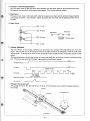
1
SERVICE MANUAL
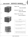
SHARP
PDSM281 007-MZ
t_
----
-
------=:::::::----..,
Dot Printer
MODEL
.
MZ-80P5 (~AeL~
~~
11-HS
e. . bH P
M.()D~L l'H-t:
i~
~Mb ~~
~~}~:)
i"-1.
I c 2'2 (
1C tG,
·~
~ AQ'"f'f([
w~Ut M.A.Y ~-.toT Bf:. 1ltf
'1l+t
\\..1
~ fo
U,..TE.~
f'~l)...l'Te ':;..)
----------------~
FEATURES
•
Printing paper
Can use fanfold paper 4-10 inches wide.
•
Character printing
Four character sizes are possible.
•
Bit image printing
Printing is possible with dot units.
•
Paging
Number of lines printed on 1 page can be determined.
•
Tabulation
Both vertical and horizontal tabulation control is possible.
•
Feed
Switch for line by line paper feed and paper feed in page units.
Control is also possible through software.
•
Copies
Simultaneous copies, up
•
Alarm bell
Alarm bell sounds to warn the user of mechanical trouble, lack of printing
paper, etc.
•
Bi-directional printing Along with bi -directional printing, there is very effective printing thanks to
the use of logical seeking. (Only 80 characters/line, 40 characters/line)
•
Printing ribbon
io 3
pages in eluding the original, are possible.
lt can be easily put in and taken out because a special cartridge ribbon
is used.
SHARP CORPORATION
~~~·-HS 2.A1"LH~
PS ?en..rrf~~
Contents
Specifications . . . . . . . . . . . . . . . . . . . . . . . . . . . . . . . . . . . . . . . . . . . . . . . . . . . . . . . . . . .
1
Precautions before servicing . . . . . . . . . . . . . . . . . . . . . . . . . . . . . . . . . . . . . . . . . . . . . . . . .
2
Explanation of MZ-80P5 . . . . . . . . . . . . . . . . . . . . . . . . . . . . . . . . . . . . . . . . . . . . . . . . . . .
3
Troubleshooting CPU board & drive PWB . . . . . . . . . . . . . . . . . . . . . . . . . . . . . . . . . . . . . . .
7
Adjustment of head driving coil energizing pulse width . . . . . . . . . . . . . . . . . . . . . . . . . . . . . .
16
1/0 card repair procedure . . . . . . . . . . . . . . . . . . . . . . . . . . . . . . . . . . . . . . . . . . . . . . . . . .
17
Power supply section . . . . . . . . . . . . . . . . . . . . . . . . . . . . . . . . . . . . . . . . . . . . . . . . . . . . . .
18
Functions of printer parts . . . . . . . . . . . . . . . . . . . . . . . . . . . . . . . . . . . . . . . . . . . . . . . . . .
20
Replacing of main printer parts. . . . . . . . . . . . . . . . . . . . . . . . . . . . . . . . . . . . . . . . . . . . . . . .
25
Replacing ink ribbon from cartridge . . . . . . . . . . . . . . . . . . . . . . . . . . . . . . . . . . . . . . . . . . .
41
Repair procedure for printer mechanism . . . . . . . . . . . . . . . . . . . . . . . . . . . . . . . . . . . . . . . .
44
Circuit diagram and printed wiring board
. . . . . . . . . . .. . . . . . . . . . . . . . . . . . . . . . . . . .. .
57
Disasse·mbled views . . . . . . . . . . . . . . . . . . . . . . . . . . . . . . . . . . . . . . . . . . . . . . . . . . . . . . .
66
Packing method . . . . . . . . . . . . . . . . . . . . . . . . . . . . . . . . . . . . . . . . . . . . . . . . . . . . . . . . .
71
Replacement parts list . . . . . . . . . . . . . . . . . . . . . . . . . . . . . . . . . . . . . . . . . . . . . . . . . . . . .
72
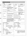
SPECIFICATIONS
• General
Item
Item
Specification
Specifications
Printing method
Impact dot matrix
Printing paper
Fanfold paper (4-10 inch wide)
Feed methos
Variable sprocket feed
Copies
Max. of 3 copies (including
original)
Kinds of characters
230 kinds (95 ASCII characters
+95 reverse characters of the 95
ASCII character +40 other
characters
Printing paper
thickness
With in 0.3mm
Character make-up
Line-to-line space
No. of digits
Ink ribbon
Special cartridge ribbon
8(H) x 9(W) dot matrix (normal
size character)
Head life
Approx. 50 million characters (14
dot character printing)
1/6 inch or determined by program
Standard interface
80 digits, 40 digits, 136 digits, 68
digits or determined by software
Power supply
8 bit parallel interface (special for
Sharp personal computer
MZ-808)
AC 220V ±1 0% 50Hz
AC 240V ±1 0% 50Hz (for UK)
Page
66 lines/page (line space mode)
or determined by program .
Printing speed
80 cps (characters per second)
(ordinary size characters)
Power consumption
75W
Working temperature 5 to 35°C
Printing direction
Storage
Si-direction (with logical seeking)
for normal size character printing
(80 characters/line) and its double
size character printing (40 characters!l-ine). For bit image printing
and other printing; u'n i-direction
(left to right).
temperatur~
External dimensions
Weight
-20 to 50°C
Approx.
377(W)
X
318(D)
Approx. 6.4 kg
Item
Specifications
Item
Specifications
CPU
Z-80A.
Timer IC
NE555
ROM
Program TMM 2732 (4K Bytes)
Head driver TR
2$D986 X 9
Character TMM 2732 (4K Bytes)
Step motor T R
2$D986 X 8
Others
Diodes, transistors
TMM 314APL-1 (2114L-1) (1K Bytes)
1/0
TMM 8255AC
Counter
Other IC's
105(H)mm
• Driver PWB Section
• CPU Board Section
RAM
X
8253AC
22 pes
• Power Supply Unit
Item
Specifications
Input
AC 220V ±10% 50Hz
AC 240V ±1 0% 50Hz (for UK)
DC 26V (21.5 to 26.5V)
DC 15V
DC 5V
Output
NOTE
-1-
Specifications and appearance are subject
to change without prior notice for improvement. In such a case, the explanation here may be a little different from
the product.
IPRECAUTIONS BEFORE SERVICING
• The printer mechanism is fixed to the chassis with two screws to keep it from being
damaged by vibration, etc. during transport. Remove these screws when using, maintaining or repairing the printer.
Fix the mechanism again with these screws when transporting the printer.
Remove the fastening screws
•
•
•
•
•
•
•
Do not apply external force to the print head, such as by touching it when it is
operating.
The print head becomes very hot so do not touch it with your hand until it cools
down sufficiently.
Do not turn the paper feeding knob (manual feed knob) when the power is on or you
will damage the paper feeding mechanism.
Do not print when the ink ribbon is loose.
When servicing and checking a printer that has been used for a long time, remove dirt,
fuzz and dust from th~ inside, and oil the mechanism.
There are two types of oil, G2 and 02. Use the proper oil for each oil point. (Refer
to page 39, 40 for oi I points.)
There are screws and nuts which are fixed and then locked with paint for vibrationproof etc. during transport. Paint the screws to lock them after disassembling and
replacing new parts. (Refer to page 39, 40 for the points to be painted to lock the
screws.)
-2-
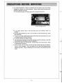
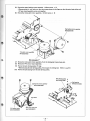
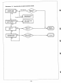
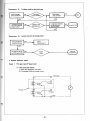
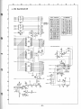
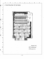
MZ-80P5 NAMES OF PARTS AND EXPLANATION OF . FUNCTI.ONS
• Names of parts
Control panel
Power switch
Appliance inlet--
----'
L-------Signal terminal (1/0 POR1
Specification panel
L...---- - - - - F G (Frame ground) term i nal
Drive PWB unit - - - - - - - - - .
r-- - - - -- - - - - - - - - CPU board unit
Switch PWB unit
-3-
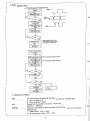
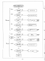
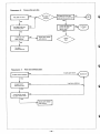
• Printer Control Flow
• Print Character Transfer Flow
When the printer receives
the character code, it raises
the signal to a high level.
• Status Check Flow
(Print character transfer routine)
(Print character transfer routine)
• Explanation of Signal
RDA . . . . . . . . . . . . The printer outputs this signal under the following conditions. (Negative logic)
1) When the power is ON.
2) When the printer is READY.
RDP . . . . . . . . . . . . Outputs from the controller to the printer. (Positive logic)
Data(RD1 ,._, RD8)strobe
STATUS . . . . . . . . . Responds in the following conditions according to STATUS demands from the controller.
(Negative logic)
1) PAPER EMPTY (1 BH + 03H)
2) Printer machanical trouble (1 BH + 04H)
-4-
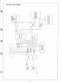
I
I
0'1
I
I
IRT . . _
1
Circuit
r----Reset
Clock
~cuit
· 4MHz
CPU
Z-BOA
D
f--
PIO
8255AC
I
>
~!l ~ :2;,:e,
"1.-~
!
D
I
§I ~>I
() -1111
Circu1t
Select
Chip
Memory Circuit
(ROM, RAM)
V
Data B!us
Add,ess Bus
Control Bus
1\ 1\ 1\
Optionla Terminal
~
r--
I
Data
>I
and Buzzer Circuit
Control SW, Indicator
Circuits
Stopping Motor
0
3
C)
~
c.c
c.;·
;::'
RDP
RQ1,..._. ROB
,------->. Head Drive and
r_
I I
Circuit f - - -
Circuit
Latch
I
OJ
0
n
a.
~
C)
0
OJ
"
STATUS
RDA
Interface Circuit
•
n
c
• Driver Board Block Diagram
Head drive
CPU
>
.>
circuit
Printer
mechanism
board
'"""!\
I
Timer
circuit
*CR step
motor and
':::>
drive circuits
'>
FEED step
motor and
drive circuits
* CR Step motor= Carriage driving step motor = Timing belt motor
-6-
!\
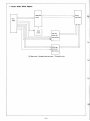
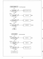
TROUBLESHOOTING CPU BOARD & DRIVE PWB
+ 5V
+15V
+26V (21.5 to 26.5V)
Check power circuit.
Check printer
mechanism
FEED, TOF SW circuit
Check FEED drive circuit
Push FEED SW
and turn power
on again .
Check CR step motor drive
circuit & printing head drive circuit
Check printing head drive
circuit & FEED circuit
Check printer interface
circuit & 1/0 card
*TOF: Top of Form
-7-
FEED, DRIVE CIRCUIT
FEED, TOF SW CIRCUIT
Connect switch PWB.
Check FEED, TOF switches
19.
>-----... and R 5, 6, 20,
for
CPU board
Check select circuit (1)
Check latch circuit
for
DRIVE PWB
Check 023, 039, 022.
2SC 1815
2SB 743
S5277B
Check connecting line &
latch circuit
Check 011, 12, 13, 14.
Check IC2
YES
Check step motor
for FEED.
-8-
2SD 986
7406
(for DRIVE PWB check)
Check TIMING circuit
Check latch circuit
555
Check IC1 and adj<;)cent
circuit
Check 020, 21 and adjacent
•I circuit
':::>
Check 019 and adjacent
circuit
I
25A 1015
25C1815
1 25C1815
Check latch circuit
Check +26V power circuit.
Check
Check printer head
-9-
01 to 8
0 1 to 8
010 to 17
RA 1
250986
1 51555
15953
CIRCUIT CONNECTED WITH.
CR STEP MOTOR DRIVE
2SC1815
Check latch circuit.
2SB743
Check +26V power circuit.
for
DRIVE PWB
Check 025, 27, 041.
~------------------~
2SC1815
2SB743
S52778
7406
Check connecting line and
latch circuit
2SD986
Check 015, 16, 17, 18
IC3
2SD986
7406
74LS14
8253
for
CPU board
IC4, 03
R10, 14, 15
2SC1815
74LS14
Check IC15, 19, 5, 17,
R17, C10.
74LS04
74LS08
74LS10
74LS74
74LS125
Check select circuit (1)
Z-80A
Check IC23
Check CR step
motor.
-10 -
8253
PRINTER INTERFACE CIRCUI"!J (For CPU board check)
'
Connect cable.
Check IC1, 3
Check IC2
74LS125
75189
Check latch circuit.
CheckiC16
I 7406
Check latch circuit.
Check IC16
Check IC11
- 11-
7406
(For CPU board check)
...__ _ _ _ _ __, Check chip select circuit.
Check IC 26
Z-80A
Check IC13
74LS02
Check IC12
74LS04
Check I C 11
8255
Check IC11
8255
(For CPU board check)
Check reset circuit.
Check I CS, 9, 10
- 12-
(For CPW board check)
Check oscillator circuit.
2MHz
Check IC26
Z-80A
Check chip select circuit.
Check IC26
Check I C23
I 8253
(For CPU board check)
Check oscillator circuit.
Check reset circuit.
Check R30.
Check each BUS line
Check EP-ROM, RAM
circuits.
-13-
Z-80A
(For CPU board Check)
Check IC26
Z-80A
Check IC16
7406
Check IC27
74LS32
Check IC26
Z-80A
Check IC24
74LS42
Check IC17
74LS08
(For CPU board Check)
Check chip select circuit
Check reset circuit.
-14-
Check IC26
Z-80A
Check IC11
8255
(For CPU board check)
Check IC26
Z-80A
Check chip select circuit.
Check IC27
74LS32
Check IC26
Z-80A
Check IC26
Z-80A
(IC22 : ROM 1)
(IC25: ROM 2)
(For CPU board Check)
Check chip select circuit.
(IC14 : RAM 1)
(IC18: RAM 2)
-15-
Check IC26
Z-80A
Check IC27
74LS32
Check IC26
Z-80A
Check IC26
Z-80A
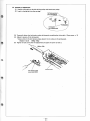
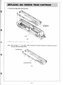
ADJUSTMENT OF HEAD DRIVING COIL ENERGIZING PULSE WIDTH
This concerns the printing energy force for the head wire to print a dot and its length in time as well. The shorter
the energizing pulse width (time) is, the smaller the printing energy is, thus · weakening printed letters. To the
contrary, the larger pulse width prolongs the printing time of head wire, thereby feeding the head with the head
wire clacking out. In most cases, the head wire is caught by the ink ribbon, and what is worse, the tip of head
wire is broken.
This adjustment is required to give an appropriate printing energy to the head wire. Make an adjustment in the
following manner.
1) Remove cabinet B. (Do not disconnect the connector of feed switch circuit.)
2) Take out the head cord PWB connector from the connector of terminal PWB. Be careful not to damage the
head cord PWB.
3) Turn on the paper end sensor. (Put a piece of paper in the paper sensor lever located at printing paper
insertion area.)
4) Draw out the power supply socket (N0504) with 5-pin lead from the CPU board.
5) Connect 3 units of D.C. power supply to the 5-pin connector (N0504) of CPU board as shown below:
24V D.C. (current capacity: 1.5A or more), 15V D.C. and SV D.C..
6) While pushing the line feed switch of the set, turn on the power switches of the three D.C. power supply
units. (The head is shifted right and left.)
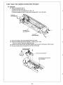
7) Connect the synchroscope to the collector of the transistor 019 (2SC1815) on the drive PWB to check to
see if the pulse width on the synchroscope is 400±1 0 J.J.sec. If the width is out of standard value, rotate the
semi-variable resistor at the drive PWB to adjust the width.
(The semi-variable resistor is to be fixed with lacquer after adjustment.)
Note: Before checking pulse width, calibrate the synchroscope to eliminate error in time base.
Head driving coil energizing pulse signal
For pulse width adjustment
0
©
Sy nch rose ope to be
connected here
(Collector of 019)
0
Drive PWB unit
0
0
0
CPU Board Un it
Connecting diagram for power supply and synchroscope
-16-
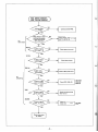
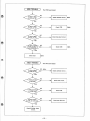
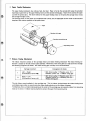
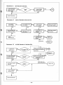
1/0 CARD REPAIR PROCEDURE
• Procedural steps
START
(
MZ-808
MZ-80P5
Mechanical
trouble
Family
check
(
Empty of paper
J
STATUS information
Check IC1, 4,
5, 7
Check IC1,
4, 6, 7, 8, 9
Check IC2,
3, 8,9
Check IC1, 2
3, 4, 7, 8, 9
YES
(
•
END
)
Checking method of printer interface circuit
1) Press insulated part of IC with finger to check
•
if it is abnormally heated . . . . . . . . . . . . . . . . . . . . . . .
•
if there is an unappropriate change . . . . . . . . . . . . . . . . .
IC improper, too large load in IC, touching
between circuits
faulty soldering, improper printed wiring
2) Use a synchroscope to check
• if input and output logics of TTL-IC do not match
• if TTL-IC voltages· are within the TTL level
Note) TTLievel: High: 2.4Vormore
Low: 0.5V or less
- 17-
Defective I C gate
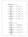
POWER SUPPLY SECTION
• Block Diagram of Power Supply Circuit
~
Smoothing
section
Rectifier
section
Smoothing
section
-
Regulator
section
Rectifier
section
Smoothing
section
--
Regulator
section
1--
AC 220V
o--
AC24 ov
(for UK)
Filter
section
Power
transformer
Regulator
section
Rectifier
section
0
+26V
(21 .5 ""26.5V)
<> +5V
~
....
-18-
--
+15V
• Troubleshooting
':>
NO
I Check power
.., transformer and input
circuit.
NO
Check 80103, F1 03,
C103, C104.
NO
CheckR101,
ZD102, Q102.
YES
Check Q101,
output connector
NO
YES
Check 80102,
F104,C105
YES
Check IC1 02,
output
connector
NO
Check 80101,
F105, C106.
Check IC101
output
connector
-19-
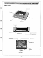
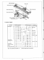
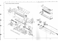
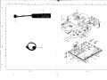
I FUNCTIONS OF PRINTER PARTS
• Exterior of Mechanism and Names of Parts
Paper sensor
Sprocket unit
Ribbon driving gear
Paper feeding motor
Print head
Timing belt motor
•
Sensing Mechanisms
Sensing mechanisms consist of HP sensor, PTS sensor and PE sensor. The HP sensor is attached to determine the
Home Position of the carriage and generates the reference signal for printing.
The PTS sensor generates the timing signal used to determine printing position. lt detects this signal and adjusts
carriage speed. The PE sensor detects the presence or absence of paper.
1.
HP Sensor (Home Position Sensor)
The HP sensor consists of the home position sensor assembly and sensor board on the lower part of the carriage.
The signal is High when the sensor board interrupts the light shaft of the photo coupler . .lt is an open collector
output)
-20-
2. PTS Sensor (Print Timing Signal Sensor)
The PTS sensor consists of the PTS sensor board assembly and the sensor board on the timing belt motor shaft.
The signal is Low when the slit of the sensor board appears. (lt is an open collector output.)
3. Paper Sensor
The paper sensor consists of the reed switch attached to paper sensor board and the permanent magnet attached
to the paper sensor lever. The permanent magnet approaches the reed switch and the signal passes when there is
no paper.
4. Sensor Circuit
To+5V
HP signal
~
Paper sensor
Reed switch
o------o~
~Permanent magnet
PTS signal
~
ToGND
• Printing Mechanism
The main elements of the printing mechanism are print head unit, carriage, timing belt, timing belt motor and
platen. The print head unit on the carriage is moved to the right and left by the timing belt on shafts A and B of the
carriage guide. The timing belt is driven by the timing belt motor through the belt driving pulley and belt driving
pulley.
Printing performs when the dot wire springs out toward the platen due to the flow of c1,.1rrent in the head driving
coil. The current flows when the PTS signal is generated by the belt motor rotation.
~--------------------~$
Carriage drive signal
HP signal
~--------------2~.5~4~m-m~(-1/-10_"_)--------------~$f
PTS signal
H d d
ea
nve coi I signal
~ C 0.4ms
---=-----
Dot wire tip
.
f
-
--~~-
1. Principle of Carriage Movement
The carriage is moved to the right and left by the drive of the timing belt motor with the timing belt inserted in
the carriage.
Carriage
Junction
Right
Timing belt
-21-
Drive for the timing belt motor is basically 2-2 phase excitation.
Sequence of the belt motor drive to move the carriage is as follows.
Carriage
From left to right
From right to left
Step
A phase
B phase
C phase
D phase
1
ON
OFF
OFF
ON
2
ON
OFF
ON
OFF
3
OFF
ON
ON
OFF
4
OFF
ON
OFF
ON
1
ON
OFF
ON
OFF
2
ON
OFF
OFF
ON
3
OFF
ON
OFF
ON
4
OFF
ON
ON
OFF
2. Printing function of the Print Head
This explanation is for the wire movement of one dot when one character is formed.
1) The function plate is pulled in to the core when current flows in the driving coil and thus the dot wire springs
toward the platen since it is connected with the function plate.
2) The forced dot wire springs out till it strikes the platen and one dot is printed on the paper through the ribbon
when it strikes the platen.
3) The function plate is reset to its former position by the force of the function plate spring when current no
longer passes through the driving coil.
The dot wire, after it strikes the platen, returnes to its position, which is connected with function plate, by its
striking force and the wire return spring and maintains itself in a waiting condition.
Dot wire
Function plate
Function plate spring
-22-
Ribbon mask Platen
•
Paper Feeding Mechanism
The paper feeding mechanism has ordinary feed, fast feed. Paper is fed by the sprocket shaft using the sprocket
transmission gear driven by the paper feeding motor and the sprocket driving gear. Paper is fed by pulling the paper
up with the sprocket pins. The drive method for the paper feeding motor is the same as the carriage motor rnoves
the carriage from right to left.
The printing position on the paper can be adjusted with a knob, but the adjustable minimum width is about 0.5mm
because of the resolution precision of the pulse motor .
..::.....::-------Paper
Sprocket drive gear
Sprocket transmission gear
Paper feeding motor
•
Ribbon Feeding Mechanism
The ribbon mechanism consists of the cartridge ribbon and ribbon feeding mechanism. The ribbon feeding mechanism is attached to the belt tension plate assembly. Movement of the timing belt to the right and left is through
the following arrangement of wheels. The ribbon driving gear normally turns counterclockwise.
Carriage movement
Arrangement of wheels
1
Left --* Right
(In direction of arrow-+)
• Belt driven pulley --* Planetary pinion ( 1) --*
Planetary pinion (2) --* Ribbon driving gear
2.
Right --* Left
(In direction of arrow
• Belt driven pulley --* Planetary pinion (1) --*
Planetary pinion (3)--* Planetary pinion (4)--*
Ribbon driving gear
L _ __ _
~)
The ink ribbon is stored endlessly in the cartridge case. This ink ribbon, pinched between the ribbon feeding knob
and ribbon pressure roller, is wound UJ3 by the ribbon feeding knob set on the ribbon driving gear.
Furthermore, there is a ribbon braking spring at the outlet of the cartridge case to. prevent the ribbon from becoming
loose as it is wound. A ribbon mask is attached to prevent the paper from becoming dirty.
-23-
Ribbon feeding knob
Ribbon pressure roller
Ribbon braking spring
Ribbon planetary gear ( 1)
Ribbon planetary gear (2)
Ribbon planetary
Ribbon driving gear
Ribbon planetary gear (4)
•
gear (3)
Connector Diagram
Connector terminal No.
Connector terminal No.
Connection
15
Print solenoid
Connection
R, T sensor (GND)
Paper sensor
11
2
2
~16
11
3
3
0 17
11
4
4
L18
11
5
5
19
Timing signal
11
6
6
20
Reset signal
11
7
7
21
CR motor A phase
11
8
8
22
" B "
11
9
9
23
" c "
10
24
.. D "
11
25
VLED (+5V)
12
26
" B "
CR motor common
line( +)
13
27
" c "
PF motor common line
14
28
" D"
Print solenoid
Common line(+)
11
Paper sensor
PF motor A phase
Note: Print solenoids are counted 1, 2 ..... 9 from the upper side of the characters.
-24-
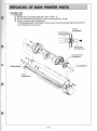
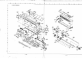
IREPLACING
OF MAIN PRINTER PARTS
1. Sprocket Unit
. 1-1 Disassembly
(1) Remove fastener for sprocket guide shaft. (4N x 2,4W x 2)
(2} Remove sprocket bearing from frame LA side of the sprocket shaft. (E ring)
(3) Remove the sprocket unit and disassemble.
1) Pull the sprocket shaft in the direction of the arrow and remove the sprocket bearing from frame RA.
2) Lift the sprocket unit up and out.
Frame RA
94V F 303003000
-+
Sprocket shaft
94VF303013010
Sprocket guide shaft
94VF303010010
Sprocket shaft
94VF30301301 0
-25-
(4) Disassemble the sprocket unit
1) Pull out sprocket LA assembly
2) Pull out the paper guide roller.
3) Pull out sprocket RA assembly.
4) Disassembly sprocket LA and RA assemblies (Remove the sprocket lock lever, sprocket wheel, paper
holding cover spring, G pin and paper holding cover.)
5) Pull out the sprocket gear (Spring pin)
Sprocket lc;>ck lever
94VF303011050
Sprocket frame
94VF303011 01 ~
1
Sprocketwh~
94VF303011020
Sprocket gear
94 V F 303013020
SP(if>2X 14)
?VB130103216
1-2 Assembly
(1) Assemble the sprocket unit in the reverse order used for disassembly.
• Note the direction for inserting LS (leaf spring).
SP(<P2X 14)
94VB130103216
Sprocket bearing
Sprocket gear
94VC601302050
94VF303013020
-26-
• Attach the sprocket wheels to have the sprocket numbers be in the same direction and same angle in
relation to the sprocket shaft.
• Note the direction for inserting the paper guide roller
Sprocket lock lever
Sprocket LA Assembly
Paper guide roller
94VF30301 0020
Sprocket gear
,-[h
Tee~cket
Sp,ocket wheel numbe,
RA assembly side
Direction for inserting paper guide roller
• Parts used for sprocket LA and sprocket RA are the same but the direction attaching the sprocket lever
and paper holding cover is different.
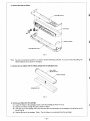
2. Print Head Unit
2-1 Disassembly
( 1) Pull the head cable from the head connector.
·When inserting or pulling out the head cable, hold the place marked with arrows ( 9 ) and move the
head cable horizontally in the direction of the arrow(~), while pushing the head connector.
Print head unit
94VF4011 00000
Head cable
Head connector
0
iJ
• •
94VA260112001
(2) Turn the head lock lever clockwise.
(3) Remove the print head unit.
2-2 Assembly
(1) Set the print head unit on the carriage.
(2) Insert the head cable into the head connector.
-27-
3. Paper Sensor
3-1 Disassembly
(1)
(2)
(3)
(4)
(5)
Remove the soldered lead wire from the terminal board ..
Stretch the bend in the outer paper guide [In the direction of the arrow.]
Remove the paper sensor lever spring.
Remove the paper sensor board assembly.
Remove the soldering of the reed switch.
Sensor board assembly
94 V F303009000
. Outer paper guide
94VF303007010
Paper sensor lever spring
94VF303007020
3-2 Assembly
(1) Assemble in the reverse order used for disassembly.
4. PTS Sensor
4-1 Disassembly
(1) Remove the sold_ered lead wire from the PTS sensor board.
(2) Remove the PTS sensor board assembly (2.5mm screw x 1 ).
-28-
4-2 Assembly and Adjustment
(1) Temporarily fasten the PTS board assembly.
(2) Solder the lead wire.
(3) Adjust the period of the PTS signal.
1) Check T period while printing.
• Check the wave form with a synchroscope.
• Check that the print head has been fitted.
T
~
•
]-J
2) Adjust the PTS sensor board in the direction shown by the arrow in the figure so that the going and
return T periods are almost equal.
3) After adjusting, fix the screw lock and paint the screw to lock it.
5. HP Sensor
5-1 Disassembly
( 1) Remove the soldered lead wire of the HP sensor board from the terminal board .
• Do not touch the timing belt the soldering iron.
(2) Remove the HP sensor board assembly (2 .5mm screw. E ring) .
t
~
~~----~
~~
- 29-
HP sensor board assembly
----- 94VF303030000
5-2 Assembly and Adjustment
(1) Attach the HP sensor board assembly
• Put in the screws temporarily.
(2) Solder the lead wire to the terminal board.
(3) Check the relation between the PTS signal and HP signal.
• Check the wave form with a synchroscope.
• Check that the print head has been set.
(4) When the phase is not right, adjust it by moving the HP sensor board in the direction of the arrow.
(5) After adjusting, fix the screw lock and paint the screw to lock it.
HP Signal
PTS Signal
I
I
0.9 - 1.2ms
6. Motor Assembly (Timing belt motor assembly, paper feeding motor assembly, belt driving pulley)
& 1 Disassembly
(1) Remove lead wires of the timing belt motor assembly from the terminal board.
(2) Remove lead wires of the paper feeding motor assembly from the terminal board.
(3) Remove the PTS sensor lead wires from the terminal board.
(4) Take off the wire band.
Wire band
motor assembly
0
0
0
0
0
0
Green Green Red White Black Yellow
For timing belt motor assembly
- 30-
Timing belt motor assembly lead cable
(5) Remove the paper feeding motor assembly. (2.5mm screw x 2)
·When removing it, only take out the two screws shown in the figure so that the motor heat sinker and
HP sensor board assembly come out together.
(6) Remove the timing belt motor assembly. (2.5mm screw x 2)
-......
Paper feeding motor assembly
94VF303031000
·~
~
'-....._~
Belt motor heat sink
94VF303026010
(7) Remove the timing belt motor assembly from the timing belt motor heat sink.
(8) Remove the PTS sensor board assembly.
(9) Remove the belt driving pulley ( E ring).
• When removing the belt driviog pulley; frrst loosen the timing belt. (Refer to page 34)
(1 0) Remove the ball bearing from the belt driving pulley.
t
Timing belt motor assembly
94 VF303027000
PTS sensor board
94 V F303029000
Belt motor heat sink
94VF303026010
- 31-
6-2 Assembly and Adjustment
(1) Attach the timing belt motor assembly to the timing belt motor heat sink.
(2) Attach the PTS sensors board.
(3) Place the ball bearing in the belt driving pulley.
(4) Put in the belt driving pulley.
(5) Attach the timing belt motor assembly and timing belt motor heat sink to the frame.
·Check the gear backlash. (C should be minimum.)
(6) Attach the paper feeding motor assembly to the frame.
·Check the gear backlash. (C should be minimum.)
''Gl
~~~
i ~ @)' \I
I
I
I
.o J
'":~
\,_>
/
·~
"0r___v
\ ./r~I
--
'~c-~
(Timing belt motor backlash)
(Paper feed motor backlash)
7. Timing Belt
7-1 Disassembly
(1) Remove the timing belt motor assembly and motor heat sinker. (2.5mm screw x 2)
Do not mix up the screws. (Refer to * mark in the figure.)
(2) Pull the timing belt from carriage assembly A.
(3) Loosen the lock screw on the belttension plate and remove the timing belt. (2.5mm screw)
Belt tension plate
94VF303019000
Timing belt
94VF303014010
Timing belt motor assembly
94VF303027000
Motor heat sinker
94 V F30302601 0
-32-
7-2 Assembly and Adjustment
(1) Hang the timing belt on the belt driving pulley and belt driven pulley.
(2) Insert the timing belt into the carriage.
(3) Temporarily fasten the belt tension plate while gently stretching the timing belt. (2.5mm screw x 2)
(4) Adjust the tension of the timing belt.
• Using the hole in the belt tension plate, adjust it to its rating on the spring scale.
[Standard value]
1300gr ±50gr
(5) Tighten the lock screw after the adjustment and paint the screw to lock it.
Belt tension plate
94VF303019000
2.5mm screw
- 33-
8. Belt Tension Plate Assembly {Including ribbon driving gear)
8·1 Disassembly
(1) Remove carriage guide side A.
1) Remove E ring on frame LA.
2) Remove the nuts on carriage shaft A. (4N x. 2)
3) Move the carriage to frame LA side and pull carriage shaft A out to the right
Frame LA
94 V F303002000
Frame RA
94 V F303003000
(2) Move the carriage to the center between frame LA and RA
(3) Remove the home position sensor assembiy. (2.5mm screw, E ring)
·There is no need to remove the soldered lead wire.
(4) Remove the lock screw for the belt tension assembly and remove the timing belt. (2.5mm screw)
(5) Pull out the belt tension plate assembly and ribbon driving gear.
-34-
(6) Disassemble the belt tension plate assembly.
1) Remove the belt driven pulley flange. (E ring)
2) Pull out the belt driven pulley.
3) Pull out the planetary lever assembly.
4) Remove the planetary pinion. (E ring x 3)
~
®
Planetary lever assembly
94VF303020000
p-~
~~lt driven pulley flange
F30301802t ·8020
all bearing
94VB210151490
Belt driven pulley
94VF303018010
"""- ,..1
e.
<!?
V
LS(3-0.07-6)
94VB101252190
~~
Planetary pinion
94 V F303020020
8-2 Assembly and Adjustment
( 1) Assemble the belt tension plate assembly.
1) Put in the planetary pinion. (E ring x 3)
• Do not make a mistake about the direction and position of LS (leaf spring).
2) Put in the planetary lever assembly.
3) Put in the belt driven pulley.
~LS(3-0. 07-6)
4) Put in the belt driven pulley flange.
_rr_
Planetary pinion
(2) Put in the ribbon driving gear and ribbon tension plate and attach the timing belt (Temporarily fasten
with 2.5mm screw.)
(3) Attach the home position sensor assembly. ( E ring)
(4) Assemble carriage shaft A in the reverse order used for disassembly.
(5) Adjust the belt tension properly. (Refer to section 7.2 on page 33.)
(6) Check the HP signal and PTS signal. (Refer to section 4.2 on page 29 and section 5.2 on page 30.
9. Platen (Including sprocket transmission gear)
9-1 Disassembly
(1) Remove the sprocket unit. (Refer to section 1-1 on page 25.)
(2) Remove the paper feeding motor. (Refer to section 6-1 on page 30.)
·There is no need to remove the soldered lead wire.
(3) Remove the sprocket transmission gear. (E ring)
(4) Remove platen A. (3mm screw x 4)
-35-
Platen A
94 V F303004000
Sprocket transmission gear
Paper feeding
motor assembly
94 V F303031 000
9-2 Assembly and Adjustment
(1) Temporarily fasten platen A to assembly LA and RA. (3mm screw x 4)
(2) Determine the position of platen A and paint the screws to lock them after fastening them.
·Determine the position of the platen then push in the direction of the arrow so there is no space
between the platen and positioning pins and then tighten the lock screws.
(3) Attach the sprocket transmission gear. (E ring)
(4) Attach the paper feeding motor. (Refer to section 6-2 on page 32.)
(5) Attach the sprocket assembly. (Refer to section 1·2 on page 26.)
Positioning pin
-36-
10. Adjusting Lever (Including adjustment of basic space between platen and print head)
10-1 Disassembly
( 1) Move the adjusting lever to the middle step in the hole in frame LA ..
(2) Remove the print head unit. (Refer to section 2-1 on page 27.)
(3) Insert a screwdriver or similar tool into the hole in carriage shaft B to stop it from turning and remove
the nuts holding it (4 N).
(4) Remove the ribbon mask and head sitting plate. (2.5mm screw x 2)
Adjusting lever
94VF303001030
Ribbon mask
94VF303001092
Screwdriver
Head sitting plate
94VF303001100
@, ~
10-2 Assembly and Adjustment
(1) Temporarily fasten the adjusting lever. (4N)
·Set it in the middle step of the adjusting hole.
(2) Attach the print head unit to the carriage.
·There is no need to insert the head cable into the head connector.
(3) Turn carriage shaft B so the hole is up.
• lt is eccentric so pay attention to the top and bottom of the eccentric part.
: :!If!~! 1 ~ -
Screwddver
I
Carriage shaft B
"vff-k-fa
I
Up
\.. \. ;1 I ,; / /
a> b
b
-37-
(4) Move the carriage to the 1 side on the scale graduation.
(5) Insert a narrow screwdriver or similar tool into the carriage shaft B hole and adjust the clearance between the dot head tip and platen by moving it forward and back.
• [Standard clearance] 0.65mm
• Position the carriage shaft where the platen and platen head tip lightly touch both sides of a thickness
gauge.
(6) Fix the adjusting lever
·Tighten it so the clearance does not change.
(7) Remove the print head unit.
(8) Temporarily fasten the head sitting plate and ribbon mask. (2.5mm screw x 2)
(9) Attach the print head unit.
• Insert the head cable into the connector.
(10) Fasten the ribbon mask and head sitting plate.
1) Adjust the adjusting lever to its uppermost step.
·Adjust it all-the way to the side marked (-).
2) Adjust the relative position of the platen, ribbon mask
and print head tip as shown in the figure.
·Check that the ribbon mask is at a right angle.
a-+-*i-b
about 0.65nm
a> b
Print head unit
Within ±0.3mm
of C (standard)
Ribbon mask
3) Put the head sitting plate approximatel y parallel to the side surface of the carriage and in contact
with the bearing. In addition, position it so it satisfies the conditions in (2) and fasten it with screws.
(11) Do not touch the home position sensor assembly and carriage sensor plate when setting the adjusting
lever to the uppermost and lowermost steps.
f
9
>0
>0
Home position sensor assembly
Sensor pi ate
-38-
A
I
B
I
c
I
I
• Points for Oiling and Painting (To lock screws)
3
/ .-·
'"---. . .
~
L
"~l!
.
~'' 0101!~;JP
~ ""~
~ ~l
~@ I
'
(LS) ·~t~
~
~'
. ,. '. "i
' !'ili
t~"'
........:.., "-
·,
·
~
.
'
"
.
~·~~
~.. . . . . 'Jr~~ ""~
G2
~t,
~
-39-
"
-40-
~(LSI
·~
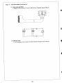
REPLACING INK RIBBON FROM CARTRIDGE
1. Remove the cartridge ribbon from the printer.
2. Remove the cartridge case lid from the cartridge case frame.
Note: There are catches ( - ) in 6 places. When removing the lid, push the catches to the outside so they aren't
bent and remove the cartridge case lid.
Cartridge case frame
Fig. 2
-41-
3. Remove the used ink ribbon
Cart ridge case lid
Used ribbon
Cartridge case frame
Fig. 3
Note:
Fig. 3 is an illustration and there is no need to remove everything as shown. If you do remove everything, the
relative positions are as shown in the figure.
4. Remove the new ribbon with the ribbon package from its cellophane case.
New ribbon
94VER-04-1/ //
Ribbon package
Cellophane case
Fig. 4
5. Put the new ribbon ~nto the cartridge.
(1) Leave the ribbon in the package and put it into the cartridge as shown in Fig. 5.
(2) Pass the ink ribbon through the path as shown in Fig. 6.
(3) Hold the top of the package with your hand and pull out the bottom of the package in the direction of the
arrow (Fig. 5).
(4) Remove the top of the package. (Note: The ink ribbon is not removed from the cartridge.)
-42-
Cartridge case lid
Ribbon
Ribbon package
Bottom of package
Fig, 6
Cartridge case frame
Fig. 5
6. Put in the cartridge case.
7. Turn the ribbon feeding rooler in the direction marked on the cartridge and check that the ribbon is not pinched
between the ribbon case.
Ribbon feeding rollwer
Fig. 7
Note: After replacing the ink ribbon, make a check on the cartridge label that indicats number of times the
cartridge ribbon has been replaced. After 5 checks, use a riew cartridge ribbon.
Example
PLATEN
INKED RIBBON
PRINT HEAD
-43-
REPAIR PROCEDURE FOR PRINTER MECHANISM
• Flow Chart to Check Cause of Defective
Phenomenon 1.
Mechanism does not function
Is it connected
to the system?
NO
Is there
printing paper?
NO
YES
Does the
mechanism function?
YES
To check of power
and control circuits.
Phenomenon 2.
Carriage does not move.
Is it connected
to the system?
Does the
carriage move?
NO
NO
YES
Does the timing belt
motor revolve?
YES
NO
NO
Is the timing belt
motor wired?
YES
Does the carriage move
when you move the timing
belt by hand?
NO
~----t-..4
To check parts
connected with power
supply.
Only timing belt moves.
Timing belt also doesn't move.
NO
NO
Belt driving pulley.
Belt driven pulley.
Is the timing belt
motor driving signal
normal?
YES
NO
1----+--_..,""'
To check of things
related with control.
Timing belt motor.
Does it move when
removing the cartridge
ribbon?
Note:
NO
Only timing belt moves.
Timing belt also doesn't move.
Active the paper to print even if there is no need to print while checking.
-44-
Phenomenon 3.
Does not print at all.
NO
Is it connected
to the system?
YES
Connect the
connector.
NO
YES
NO
Is printing command
outpu_t?
OK
Does it print?
J
-
To check parts
connected with
control.
YES
NO
Is there printing
paper?
YES
Does paper sensor
function normally?
~
.
*
NO
To Phenomenon 7.
~epla~eas
YES
Does carriage move?
NO
n sect1on 2-2.
To Phenomenon 2.
'
YES
Is print head unit
connector connected?
NO
Connect the
connector.
YES
YES
YES
Is print head driving
waveform normal?
r
Does it make any
function noise?
YES
NO
To check of things
connected with
control.
Is +26V supplied
to print head?
NO
NO
To check the parts
related
with power supply.
NO
~
@
Is printing done
on copy paper?
NO
Move the
adjusting lever to the
lowest step.
YES
YES
Is the cartridge ribbon
put in correctly?
Does it print by merely
adjusting the
adjusting lever?
NO
~
Repai,as
section 10-2.
J
Put the
cartridge ribbon in
correctly.
~*Remove the paper and check if there is a "clicking" sound when the sensor lever approaches the reed switch.
-45-
Phenomenon 4.
Ribbon does not feed.
Does carriage move?
NO
Is ribbon fed?
To Phenomen on 2.
NO
YES
Is cartridge put
in correctly?
NO
-
YES
OK
l
Put cartridge
in correctly.
YES
Does cartridge knob
turn by hand?
NO
YES
Is ribbon fed when knob
turns?
Remove cartridge.
Does knob move with
only the cartridge?
YES
~
NO
J
NO
YES
Does knob turn when
ribbon moves.
NO
YES
YES
Does knob turn only
when cartridge moves
from left to right?
Does ribbon driving gear
turn when cartridge is
removed?
I
YES
NO
Does knob turn only
when cartridge moves
from right to left?
YES
-46-
NO
I
To Repair
3
Phenomenon 5.
Paper does not feed.
NO
Is it connected to
the system?
-
YES
Connect
the connector.
Does paper feed?
NO
YES
Are paper holes out
of sprocket pins?
<§>-
YES
.
NO
YES
j
'
*1
Is there an abnormal
load at the paper feedin inlet?
YES
Has paper run out?
1---
NO
Alright for a time but
paper feed ends soon?
NO
To Repair
4.
""'
..,
YES
NO
*2
Is paper sensor
functioning properly?
NO
To Phenomenon 7.
Lighten load.
YES
Is paper fed
after printing?
-
Check parts related
with control.
NO
Is paper fed when
sprocket gear is
tu med by hand?
~
Does motor heat up
when electric signal
is sent?
YES
"""'
To Repair 5
~
I
YES
NO
Does the paper feeding
motor shaft gear also
turn at the same time?
YES
Wire
according to
section 6. ~
Is the paper feeding
motor wired?
"""
YES
Is +26V su pp I ied to
paper feeding motor?
NO
~
Check parts related
with power supply.
YES
Is paper feeding motor
driving signal normal?
NO
--
Check parts related
with control.
YES
Paper feeding motor.
""'
Replace as
in section 6 .
......_
~
* 1 Check if there is a load on the paper when it is in the paper box, system case, etc.
*2
Remove the paper and check if there is a "clicking" sound when the sensor lever approaches the reed switch.
-47-
Phenomenon 6.
Prints on the same line.
Has paper run out?
NO
Alright for a time but
soon prints on same Iine? t-- -- - - - - - 4
YES
YES
NO
Are paper holes out
of sprocket pins?
Is there an abnormal
load at the paper
feed-in inlet?
YES
YES
NO
Check parts related
with control.
Is there LF, FF
paper feeding?
NO
To check
Phenomemon 5.
Phenomenon 7.
Prints even without paper.
Is paper sensor attached?
Attach paper sensor.
NO
YES
~
Is paper sensor
lead wire wired?
Lead wire soldering.
NO
YES
Is reed switch moved
by paper sensor lever?
NO
YES
Check parts related
with control.
-48-
Section 3-2.
Phenomenon 8.
Paper feed pitch is abnormal.
Is there an abnormal
load on the paper
feed-in inlet?
YES
YES
NO
Check Phenomenon 6.
Phenomenon 9.
Density of characters varies across line.
NO
Is PTS signal
period regular?
Is PTS signal output
level normal?
YES
NO
YES
Does cartridge move
smoothly by hand?
YES
a
Is +5V supplied
to PTS sensor?
NO
Check parts related
with power supply.
YES
Check parts related
with control.
YES
Is it normal if PTS
waveform amp is
changed?
Check parts related
with control.
NO
NO
Is contact of PTS
sensor lead wire
alright?
Check
Phenomenon 2.
YES
Wire as
in section 4-2.
NO
PTS sensor.
Replace as
section 4 .
in
....._
Phenomenon 10.
Fast digit characters of printing shifts.
YES
Is position of
paper correct?
After a ~ime i_t slips ~ith
no relat1on With prev1ous
correction.
I N01
1 N~
YES
---
---
A re both right and left
sprocket lock levers
securely locked?
INO
YES
Is HP sensor securely
fastened?
Check that it has
same period as PTS.
I NO
YES
Does it have same
period as PTS?
I NO
YES
Check Phenomenon 9.
-49-
-I.O
~
Phenomenon 11.
Printing paper is dirtied by ink ribbon.
After a time does
it get dirty again?
Is ink ribbon
loose?
NO
YES
NO
Is ink ribbon
path correc t?
NO
YES
Is ribbon mask
attach ed correc tly?
NO
YES
Is scale pressing
paper firmly ?
NO
._...._c
YES
Is clearance correc t after
adjust ing with adjust ing
lever?
Is clearance betwe en
print head and platen
correc t?
YES
YES
Is it correc ted when
cartr idge ribbon is
changed?
NO
YES
NO
Is paper guide plate
A put in correc tly?
NO
1-- --- --- --- --- --- +- --- ---
YES
Is paper put i n
correc tly?
NO
YES
Is paper within
standards?
-50 -
--- --- --- --t
Phenomenon 12.
Printing is light.
Is ink ribbon almost
used up?
YES
Does it immediately
become light again?
NO
NO
YES
Is the cartridge ribbon
put in correctly?
NO
YES
Is ribbon fed when
carriage moves left
and right?
NO
Check
Phenomenon 4.
YES
Is clearance between
tip of print head and
platen correct?
Is clearance correct
after adjusting with
adjusting lever?
NO
~
YES
YES
INO
Is paper within
'standards?
Phenomenon 13.
I
•
<::.
Printing is light and dark.
Is clearance between
tip of print head and
platen correct?
Is clearance correct after
adjusting with adjusting
lever?
NO
YES
YES
Does light and dark
printing disappear?
NO
-51-
~
1 YES
•
Phenomenon 14.
Same dots only are usually (sometimes) omitted.
Is contact of head
connecto r alrigh t ?
NO
Head cable side.
YES
Terminal board side.
Is correct head driv ing
signal outputted ?
NO
Check head connecto r
and 3210 cable A .
Check things related
with control.
'YES
lsdotw i re
bent?
YES
NO
Is driving coil inside
head disconnec ted?
YES
1----+ ----.<
NO
- 52 -
Phenomenon 15.
The ribbon winds but becomes loose.
Is printing paper
within standards?
Does ribbon
feed correctly?
NO
YES
NO
YES
Is clearance between
tip of print head and
platen correct?
Is clearance corrected
by adjusting with
adjusting lever?
NO
NO
YES
Phenomenon 16.
Go/return time for the carriage varies.
Does carriage move
smoothly by hand?
NO
Check
Phenomenon 2.
YES
Do phase of HP signal
and PTS signal match?
1NO
..::"
• Practical Method of Repair
Repair 1
PTS signal is bad, HP signal is bad
(1) Check points and method
1) Check +5V. [Standard] +5V ±5%
2) Test whether LEDs are normal or not.
+5V ± 5 %
,- --------,
I
1
I
I
<
~
PTS signal
I
I
I
I
I
PTS sensor
l
_j
~._ -
I
__ _j
-53-
the light shaft to the sensor plate.
3) Check the wavefor m output by opening and intercep ting
'---.
~l
I
PTS sensor side
HP sensor side
:::~--'----....,....11
(2) Method of Repair
1) Check the parts related with the +5V power supply.
sensor board assembl y.
2) If there is no continu ity between a-b, exchang e the PTS
board assembl y.
sensor
HP
the
e
exchang
b-e,
3) If there is no continu ity between
Repair 2
Timing belt does not move
(1) Check points and method
and timing belt motor shaft.
1) Check the backlash of the gears on the belt driving pulley
ry pinion and ribbon driving gear.
planeta
pulley,
driven
belt
2) Check meshing of gears between
(2) Method of Repair
1) Adjust the backlash . (Refer to page 32.)
parts and readjust .
2) If damage , or wear, to the gears, etc. are found, replace the
Repair 3
Ribbon driving gear does not turn
(1) Check points and method
1) When ribbon driving gear does not turn by hand
ry pinion and ribbon driving gear.
(a) Check meshing of gears of ribbon driven pulley, planeta
to right or right to left.
left
either
moves
2) When ribbon driving gear turns when carriage
pinion.
ry
planeta
and
y
(a) Check meshing of planeta ry lever assembl
(b) Check the reversed revoluti on of the planeta ry lever.
(2) Method of repair
the parts and readjust .
1 ), 2): If damage , or wear to the gears, ·etc. are found, replace
Repair 4
Paper feeding path is normal but paper does not feed
(1) Check Points and Method
are fixed correctl y.
1) Check if the right and left position s of the sprocke t wheel
y.
correctl
2) Check if the paper holding cover is holding the paper
-54-
3) Check if the paper holding cover spring is damaged or fallen off.
4) Check if the sprocket lock lever is securely locked.
(2) Method of repair
1) Correct sprocket wheel positions. (Refer to se·c tion 27 .)
2), 3), 4): Replace the parts if transformation, wear, etc. are found in any parts.
Repair 5
Paper feed motor gets hot and paper does not feed
(1) Check Points and Method
1) Check the backlash of the gear on the paper feeding motor and the sprocket transmission gear.
(Refer to section 32.)
(2) Method of repair
1) If damage, or wear, to the gears, etc. are found, replace the parts and readjust.
Repair 6
Scale does not hold paper correctly.
(1) Check Points and Method
1) Check if scale springs Land R are off and if there is wear, etc.
(2) Method of repair
1) If damage, etc, to scale spring Land R is found, change them.
Repair 7
Paper guide plate A is bad.
(1) Check .Points and Method
1) Check if paper guide plate A is twisted and if there is a space between it and the platen.
(2) Method of repair
1) If paper guide plate A is deformed or if there is a space between the platen and it, change paper
guide plate A.
2) Replacement procedure
1. Move the carriage to the graducation 80 side of the scale.
2. Move the scale to the print head unit side.
3. Remove lock screws (3) of paper guide plate A.
4. Remove paper guide plate A by lifting it up from the side opposite the carriage.
5. Put a new paper guide plate A in from the carriage side.
6. Tighten lock screws (3) for paper guide plate A.
-55-
Repair 8
Check abnormalities of print head unit
(1) Che~k points and Method
coil. [Stand ard] approx . 22r2/c oil
1) Measure the DC resista nce of the print head unit
3
7
I
5
9
4
8
6
2
3
7
6
2
(2) Method of repair
rd, change the print head unit.
1) If DC resista nce of the coil does not indica te standa
•.
-56 -
(
A
I
B
c
E
D
F
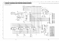
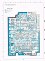
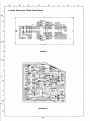
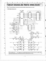
CIRCUIT DIAGRAM AND PRINTED WIRING BOARD I
Notes:
0
N
M
L
K
J
H
G
The circuit diagram and printed w iring board subject to change without prior notice.
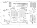
• CPU Board Circuits (1)
To OPTION UNIT
40 P CONNECTOR
J ~,,.,_____________,
~;~g;~=?Tr-=rrrr=r=rrrrlrrr=rr=rrrrrrr=rr=r=rrrrrr=rr~
2
11!-----'
RESE T -- - - - '
f.iREQ - - - - - - '
Wlf
----,
R"O
R
~~~.
IC16
-
R!!
IK
11(
lc2a lc:n
IC24
TriT -------------~
lOOp
IC27
LS32
7
6
!I
4
11
R31
IK
~8
9
IC 16
06
0~
l
R29
330
L_j3
~
~
LS42
elll!
~
Jj
4MHz
IC 26
Z- 80A
(00801
4
~
I
~~OPTIO N
13~2R23
IORO
MI
3
~
MREO
0
~
00
ICI7
08
10
3~4
8
2 3
c
-
CS!!
CS4
CS3
CS2
C'S I
9
B
I
0
A
PAO
!I
2
I
6
CSjl!l
4IC17
08
ICII
82!1!1AC
PA 1
PA l
PA 2
PA2
PA3
PA4
T.S
PRINT
PAo
11! 1
PAl
2MHz
151~~~~
5
PAT
*
IC7
LS I2!1
"f>'-'-+- - --____z§J RESE T
PCO
16
PCI
PC I
~--+--- cse
PCI
PCS
PC4
PCo
PCe
R2
IRT
6
PCT
~
I
IC2
7!1189
C2
2200PF
;:n
iN'f
PBo
R
I
I C4
LS 14
PBI
PBI
0 1
PBa
RES182!1!11
CS3
RES
§
PB3
iiR
P94
1ili
PBo
CS
PBe
RESET
PBT
7
T
ICI6
06
2 1~~ L
1
8
csl-a-
TMM314APL - I
OATEjl!lf5
14
GATE I
OATE2
1
o
T.$
1
10
CS2
CSi
4WR
NMI~IO
E - - T.S1
;-c;;--1
NMIC
_....._ _,.R(j
11
-57-
I I 2 I
3 I 4 I
+&V
OPTION
All
!I I 6 I
A11
A 14
7 I 8 I
A11
111
9 I 10 I
A1e
04
11 I 12 I
A4
Os
131 14 I
As
De
1!11 16 I
A2
De
17 I 181
AI
AO
191201
Ao
Ae
21 122
I
Dz
Ar
231 22 I
DT
M1
2!11 26 I
Do
RESET
271281
Ae
29130
A 10
31
+!IV
9
cs.s
CONNECTOR
OPTION
8
-58-
I
Wlf
I 321
331 34 1
I
ADR
01
INT
A•
MREO
iOlfO
lflj
3!5 I 36
ONO
371 381
ONO
ONO
391 40
I
ONO
p
A
c
B
E
D
G
F
H
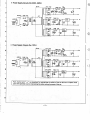
• CPU Board Circuits (2)
PAo
DRIVE
2
PA!
i
PA4
I
PAe
3
5
PAl
5
PA7
IC5
LS12!1
y
i
si
12
7 1
!!
8 1
2
9]
~
K
R3~
PCo----oc::!~~-~-mr--
I
10
IK
12
11
PIN2
3
4
PIN3
!I
6
PIN!!
I2!!P
I
(1/0 CONECTOR)
PINS
7
8
PIN7
I
GNO: 13'¥2!!
PINS
9
10
PIN9
IRDe
ATCP
11
12
PE
I R06
I RD7
T.SIG
13
14
R. SIG
VL
I!!
16
PMIA
PM 18
17
18
PM2A
10
IRPP
PM28
li
20
HOLD I
!..i-<>
12!-o
I RDA
HOLD 2
21
22
HOLD3
IS'TATUs
+!!V
23
24
+!IV
IIRT
+15V
2!1
26
+ 15V
+26V
27
28
GND
+26V
2i
!0
GNO
+26V
31
32
GNO
PRINT
33
~
GNO
IRT-!Q.l...o
L_
1
_j
13
-,IlD
~~
PIN I
PIN4
IC16
06
~·-------------------------
2
IRD4
CONECTOR
. rl !I ,jl
1
20
1/0 CONNECTOR
CONNECTOR
I
I
: ROe
11_
RS2
:
4
!le!!CLR
IRD•
GND
13
1
3D
1
40
11 !ID
::: r!lllll : I
1160
' 1 70
5
P87
~e
11 BD
•
1 1 I
I I
I
I
I
___ _ ________ Control Switch, LED, Buzzer ______ _ __________________________ _
CLR
p
=----;&
R~:)l""_k~WI
+26V
RIB
2.2K
270{1
01
!Gl
R4
6
120:
~
SW2
R3
3 .3K
Q2
""'
RZ
IOK
~ 1 ~~-------,
2SC I81S
IK
2SAIOI!I
11
~·I
7
IIIIIIII
~
ID
20
3D
4D
IC i
LS273
1or£-
1.l....o I PIN
=e~
~ IPIN3:
~ IPIN4~
~ 1PIN!!if
~
2o~
r!...o
.!!.!...a
i...o
60 IS
70 16
80 19
8
1
IK
1
' - - - - - - - '-'-1"-ot !I!I!!CLR
!10 12
!ID
Re
( 34·Pin connector)
hi
lol o
I
I
IPIN2:;
I PINS;
I PIN 7 : ·
I PINS::.
I PIN 9
11..:...
,...------'-'
1-o I ATCP
~
I PRINT
r-c'_j
I
RESET
I
T.S
rn
~7
CS3
R.S
Az
IC13
02
4
91
~
0
. m;
IC7
R9
I!IK
1!10
OPTION
8
2
RIO
15K
RI!!
IC12
04
T . SIG : - R. SIG I
I
10
IC12
VL I
RS
11
-59-·
ICI3
02
ICI2
04
A
8
c
E
D
F
H
G
• PWB (CPU Board Section)
Perspective View
2
D
Parts-fitted face
D
Opposite side
3
4
5
6
7
8
9
10
•
11
-60--
0)
.....
I
I
I
o-r-
0
~~
I I
I
I
I
~~~~
o-t--t------,
c>-J---+-·
0--'--t-----,
I
0--'--t---~
PRINT ! 0 I
ATEPI
I
I
PIN 91
PIN 7!
PIN 61
PIN 4lI
PIN 5 j
PIN 3!
PIN 2 1 <>-1--t--~
0
14
,.,.,
I
:
le
1 1
r1ZKi II
<.o
+26V
·~~~~T ~~~~6-4=~~
D26
5!12778
I "f"' '"I'£""
~,) I "f""" IIZ2'1 I
' -w -
I
•o I lr'\
...
00
I
06
5
1
I
6
e
7
PIN 4
PIN 6
26
29
30
ze
27
29
:51
:5:5 34
'I" !IV
+I !IV
+26V
+26V
+26V
PRINT
32
22
24
21
23
HOLD 2
2D
19
17
19
16
PM 18
14
13
15
T
VL
PM 28
12
11
10
B
4
2
I
3
PIN 2
R
PE
PIN9
PIN 7
PIN !I
PIN 3
PIN I
GND
GND
GND
GND
'I-I !IV
+!IV
HOLD:S
HOLD I
PM 2A
PM lA
CONNECTOR
5!1!1CLR
9
·
L - - _ _J
29
26
27
12
24
22
VB24 --Lo14
ATEP
I
I
I
I
I
I
I
I
I
I
-
Rl2
1.2K
HDLD2
VB24
21~r--+----~
2D0
IQQ I
VA24-+1:5
I
I
: 09
OB
r-f-oiD
I
I
I
l&o-1---
17
15=H
16
I
'U+, ": ~
PIN 8
PE
~
I
w
0
+26V
I
-
IPMIA
CN I
r--,
!'V
I
:::;·
c
;::;:
Cl
""0
~
:::·
CD
•
..,c
:HOLD 2
IHDLD:S
~J
--t-0
~IHOLDI
----to
jPM29
:PM2A
IPMIB
en
(")
r-----,-~7
,,
T
I
r<'l
'-------1--<14
I
VL R
i =?=i::f=?J
U1
(")
CN2
CNI
0>
,----1
'-------1--c :5
-....!
I
G>
.,
m
0
('")
(lJ
)>
A
c
B
E
D
H
G
F
• PWB (Drive Board Section)
2
3
4
5
Perspective View
D
D
6
7
Parts-fitt ed face
Opposite side
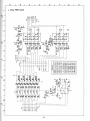
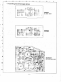
• Power Supply Circuits
~T101
1- - - -
I
I
8
8010 3
- -
-
-
I
I
I
I I
I I
I
I
I ' - - - - - -'
I
FUSE F101
+
I
I
26V
C107
33351
I
I
,1. SW101
S4VB10
r----- 1
- 1
rr-~~~~~--~--~-c>
T. F
5V
9
I I
I
+
I
-
I
'--
C101
1001"
101
--- --·
0
10
15V
+
-
C110
100.1"
251
I
I_---- ----·
11
of the set. Be sure to replace these
Parts marked with " L!',. " are importan t for maintain ing the safety
of the set.
parts with specified ones for maintain ing the safety and performa nce
-62-
8
A
c
D
E
G
F
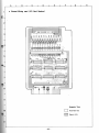
• Printed Wiring Board (Power Supply Section)
•
2
3
5
I
PRIMARY
6
7
8
9
10
SECONDARY
11
-63-
H
I
0)
~
9
10
Al2
All
17
18 EX RESET
19
20
21
2~
A4
A3
A2
AI
AO
GNO
--------------
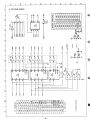
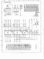
l/0 CARD lor PRINTER
A : PARTS SIDE
GNO
NMI
EX WAIT
EX INT
RESET
lEO
16
A5
-
lE I
HALT
1!5
14
GNO
MREQ
WR
MI
BUSfl$
07
06
A6
A7
13
8
Al3
A8
IOREQ
7
Al4
11
6
Al5
12
RD
!5
GND
A9
D!5
4
DO
AIO
04
3
Dl
03
D2
+!5V
I
2
+!5V
B
I
CONNECTOR
0
A
I /0
__..
__..
DO
Dl
D2
D3
D4
D5
D6
D7
<0
ID
20
3D
ID
2D
5
RO
I
CLEAR
13
12
~
4
I
I
I
I
I
_1ol
-~6
~a
IC8 7416
V
V
V
V
~
--
I
I
"""'-121
I
_,.,_21
-
~
RDA
IRT
RDP
-
15 A
14 B
13 c
CO
IC4
LS42
2
IC7 LSO"'
I
I
I
~~-J
'"
220.{1
I/2W
Jio 390Jl
1/4W
...
:
)
I
lOO
p
_v__
NOTE
STATUS
2
4
3
5
5 _6
2
I
H5V
..
..
3
,
1nn
100!
~
220.{1
I/2W 56/l I/4W
3900.
"'I/4W
~
.,~
•
.
11
10
9
8
7
GNO
13
STATUS 12
RDA
IRT
RD8
RD7
RD6
6
5
4
RD2
RD3
2
I
25
24
23
22
21
20
19
18
17
16
15
14
GND
GND
GND
GND
GND
GND
GND
GND
GND
GNO
GND
GND
CONNECTOR
ROI
RDP
PRINTER
IC7
LS04
en
;:::t'
c
(")
n
::;·
3
Q.
4
~
...
0
•
'-
5
6
12
11
1\J
RESET~RST
AO
WR
RD
A3
A2
AI
A4
A!5
A6
A7
IOREQ
w
RD5
VI
VI
V
V
RDI
RD2
R03
RD4
R0!5
R06
RD7
ROB
~
R04
+!5V
L __ _j
I
....:JL :
WO
I
113
I
I
I
I
~
I
I
Ill
I
1!5
I
19
~I I
I
"
_j
,--,
L __
..., 41
I
V
V
V
(]1
tc5
ILSI25A
;a~,
I
"""'-1ol
Ill
I
I
I
I
~61
I
I !5
I
I
....._a
19
riC9 7416
--:-r
0'>
1
RST
_!_
~
3Q 6
9
CLOCK
I"SJT
I
Ill
I
I
~
9
14
403
CLEAR
IC6
LS175
3
iQ
2Q 3
3Q 11
CLOCK
IC2
LSI7!5
~
4Q6
CLEAR
9
IQ 14
2Q 3
4QII
CLOCK
IC3
LSI7!5
"'-J
4Q 6
r=--J
2
3D
~ 40
13
4
12 3D
!5 40
13
4
12
!5 4D
CO
I
G'>
,
m
0
()
lro
I:J>
D
a::>e:} pan!:}-SlJed
D
ap!s al!SOddQ
-gg-
OL
Ma!/\ 9A!l:»9dSJad
6
8
L
9
9
l
a
3
H
8
B
A
1
.c
E
D
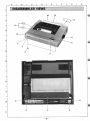
DISASSEMBLED VIEWS
2
--[
([D
8
8
3
4
5
6
7
8
9
10
11
-66-
F
G
H
A
8
c
D
E
F
G
H
J
K
L
M
Changed to [PR DAR0043PAZZ]
(Sub Radiator) during production.
(IC102, Si3552 are attached
to Sub Ragiator.)
The secondary lead wire of main
transformer will be passed between
the transformer and the secondary
power board.
2
3
4
Ill
Ill I
IIll
5
6
7
8
9
10
1l
-67-
-68-
N
0
p
I
CJ)
I
0
I
......
I
CO
0
00
U1
•
""C
...
:r
s...
0
z
r
:c
m
.. )>
A
c
8
F
E
D
G
H
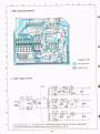
PACKING METHOD
2
~~--
d~ ~Pack;ng
3
Instruction manual
(Sometimes not packed
in same case.)
Screw ~
r&
o-~-:!S"''P<
AC .Cord
(0ACCK0050AFZZ)
(0ACCB0001 PAZZ)
(for UK, SESA)
Add. L
(SPAKA0043PAZZI
Sack
4
issAKHoo33PAzzJ A
MZ-80P5
5
•
Paper guide
(DGiD-0005PAZZ)
Packing Add.R
(SPAKA0044PAZZ)
6
7
Pack ing case
(SPAKC0125PAZZ) ..____ _ _ __
Sleeve
(SPAKS0069PAZZ)
8
9
10
11
-71-
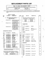
REPLACEMENT PARTS LIST
•HoW TO ORDER REPLACEMENT PARTS"
To have your order filled promptly and correctly, please furnish the following information.
1. MODEL NAME
2. REF. NO.
3. PART NO.
4. DESCRIPTION
NOTES: Be sure to use regular parts for securing the safety and reliability of the set.
portant for maintaining the safety of the set .
safety and performance of the set.
Parts marked with " .::t:. " (D) are imBe sure to replace these parts with specified ones for maintaining the
MODEL MZ-80P5
REF.
NO.
PART NO.
DESCRIPTION
CODE
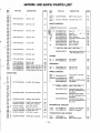
* * * CPU BOARD UNIT· SECTION * * *
OPWB-0215PAZZ
REF.
NO.
PART NO.
DESCRIPTION
CODE
R21
s
VRO-SC2EF1 02J
1 Kohm, 1/4W
AA
VRO-SC2EF151J
150 ohm, 1/4W
AA
R9 }
R10
VRO -SC2EF153J
15K ohm , 1 /4W
AA
R11 }
R14
VRO-SC2EF472J
4.7K ohm, 1 /4W
AA
:~ ~}
VRO-SC2EF222J
2.2K ohm, 1 /4W
AA
R13}
Rl6
VRO-SC2EF272J
2.7K ohm, 1/4W
AA
R24}
R26
R25
R27
R29
R34
VRO-SC2EF221 J
220 ohm, 1 /4W
AA
VRO-SC2EF561 J
VRO-SC2EF182J
VRO-SC2EF331 J
VRO-SC2EF150J
560 ohm, 1/4W
1.8K ohm, 1/4W
330 ohm, 1/4W
15 ohm, 1/ 4W
AA
AA
AA
AA
R23
R28
R30
Assembled CPU Board Unit
(Not replacement item)
s
INTEGRATED CIRCUITS
R33
R35
!Cl }
IC3
IC6
IC7
IC2
IC4
RH-iX0141 PAZZ
SN74LS125N
AG
RH -iX0086PAZZ
RH-iX01 02PAZZ
SN75189N
SN74LS14N
AN
AM
RH -iX0074PAZZ
SN74LS04N
AE
ICS]
IC9 ·
IClO
RH-iX0250PAZZ
SN74LS273N
AO
IC11
IC13
RH-iX0136PA.ZZ
RH-iX0071 PAZZ
8255AC
SN74LS02N
BA
AE
RH-iX0226PAZZ
RAM2114L-1
AY
RH -iX0079PAZZ
RH-iX0038PAZZ
RH-iX0075PAZZ
RH-iX0076PAZZ
RH-iX0127PAZZ
OPROMOOOSPAZZ
RH-i X0 146PAZZ
RH -iX01 04PAZZ
OPROM0009PAZZ
RH-iX0228PAZZ
RH-iX0078PAZZ
SN74LS74N
SN7406N
SN74LS08N
SN74LS10N
SN74LS107
ROM TMM2732
8253AC
SN74LS42N
ROM TMM2732
CPU ZSOA
SN74LS32N
AG
AG
AE
AE
AG
BP
BC
AH
BP
BG
AF
:~~2}
IC21
IC14}
IC18
IC15
IC16
IC17
IC1 9
IC20
IC22
IC23
IC24
IC25
IC26
IC27
R18
}
01
02
}
VS2SC1815//-1
2SC1815
AB
}
Rt 1
R6
Cl
C2
}
VCKZPR 1 HF222P
2,200PF. 50V, Ceramic
AA
C3
C9
C4
}
VCKZPRl HF103P
0.01 MFO , 50 V , Ceramic
AA
~~0
C15
s
VH01S1555//1A
151555
AA
RESISTORS
R1
R2
R7
R3
CAPACITORS
C5
C6
TRANSISTORS AND DIODES
01
02
03
:~7}
R19
R20
VRO -SC2EF471 J
470 ohm, 1/ 4W
AA
VRO-SC2EF223J
2'2 Kohm, 1 /4W
AA
I
}
C25
CS
C11
C12
C1 3
VCEAAU1CW476Y
47MFO , 16V, Aluminum
AB
VCEAAU 1 HW1 05R
1 MFO, 50V , Aluminum
AB
VCTYPU1B0104Z
0.1MFO, 12V, Ceramic
AB
VCSACUl VE105K
VCCCPR 1 H31 01 J
VCEAAU1 EW107M
VCEAAU1AW107M
1MFO, 35V, Tantalume
1OOPF, 50 V, Ceramic
100MFO, 25V, Aluminum
100MFO, lOV, Aluminum
AC
AA
AB
AB
Crystal, 8 MHz
25-Pin Terminal
34-Pin Terminal
AN
BF
AS
MISCELLANEOUS
X'TAL
Z0086
Z0083
-72-
RCRSA0009PAZZ
OPLGZ0086PAZZ
OPLGZ0083PAZZ
MODEL MZ-80P5 PARTS LIST
REF.
NO.
PART NO.
Z0084
OPLG Z0084PAZZ
DSOCN0138PAZZ
OPLG N0504CEZZ
OSOC Z001 OPAZZ
OSOC Z0012P.AZZ
N0504
DESCRIPTION
'CODE
40-Pin Terminal
Lead Wire with 7-Pin
Socket
5-Pin Terminal
24-Pin IC Socket
40-Pin IC Socket
I
AT
AH
R3 }
R10
R4
R5
R6
R9
R7
R8
AB
AF
AH
}
* * * DRIVE PWB UNIT SECTION * * *
DPWB-0216PAZZ
IC2 }
IC3
RH-iX0038PAZ Z
SN7406N
I:: I
TRANSISTORS
s l
01
08
011
~
o\8
J
I
VS2SD9861 I I -1
2S D986
I
AF
019)
021
023
VS2SC1815II-1
2SC1815
AB
025
020
VS2SA 10151/-1
2SA1015
AC
022}
026 "
VS2SB743III-1
2SB743
AE
027
}
oso}
o;g
10K ohm, 114W
AA
15K ohm, 1I4W
1 K ohm , 114W
AA
AA
2.2K ohm, 114W
AA
3.3K ohm, 1I4W
680 ohm , 2W
AA
AB
VRD -RU2EE122J
1.2K ohm, 1I4W
I AA
R~3}
VRS-PT3DB821 J
820 ohm, 2W
I AB
R15
RA1
R R-KZ0060PAZZ
Resistor Arry
3 .3K o hm x 9
Resistor Arry
1.2K ohm x 6
AD.
R19
RA2}
RA3
VO LUME
RR-KZ0061 PAZZ
RVR -M0038PAZZ
AC
Variable Resistor, 22K ohm I AE
CAPACITORS
s
C7
C3
C4
C8
C9
)
}
CN1
CN2
VHD1 S1555ll1 A
1S1555
VCKZPR1 HF103P
0.01 MFD, 50V, Ceram ic
I AA
VCEAAU 1 CW1 06Y
10MFD, 16V, Aluminum
AB
VCOYKU1HM104K
VCKZPU1 HF1 02P
0.1MFD, 50V. Film
0 .001 M FD, 50 V, Ceramic
AB
AA
34 -Pin Soc ket
28 -Pi n Soc ket
AX
AL
* * * SWITCH PWB UNIT SECTION * * *
VHD1 S953lll-1
1S953
l
0 8
RH-DX8402YAZZ
S5277B
f1
D35
D37
s
I
I AB
I
01
02
D1
D2
I
RESISTORS
D42
VHD-1Z24 //I-1
1Z24 , Zener
AD
VHD05Z5R6U /-1
05Z5.6L/U, Zener
AB
ZD6
ZD7
RESISTORS
R1 }
R2
DPWB-0217PAZZ
AB
Assembled Switch PWB Unit
{Not replacement item)
TRANSISTORS AND DIODES
D26
Zf1)
OSOCZ0023PAZZ
OSOCZ0017PAZZ
AA
D8
D17
D36
VRD -RU2EE103J
VRD-RU2EE153J
VRD -RU2EE102J
MISCELLANEOUS
DIODES
D~
CODE
VRD-RU2EE332J
VRS-PT3DB681 J
Cl
C2
C5
s
I
)
I
NE555
DESCRIPTION
VRD -RU2EE222J
R 12
R16
-
INTEGRATED CIRCUITS
RH-iX0134PAZZ
PART NO.
R11 )
A ssemb led Drive PWB Unit
(Not replacement item)
IC1
REF.
NO.
VRW-KT3HD121 J
R1
R2
R3
R4
R5
VS2SA 10151l- 1
VS2SC 18151l- 1
RH -PX0047PAZZ
RH-PX0033PAZZ
VRD -SC2EF102J
VRD-SC2EF1 03J
VRD-SC2EF332J
VRD-SC2EF121 J
VRD-SC2EF271J
2SA 1015
2SC1815
LED (Green)
LED (Red)
AC
AB
AD
AD
1 K ohm, 114W
1OK ohm, 1I 4W
3 .3K ohm , 114W
120 ohm , 1I 4W
7,.70 ohm, 1I 4W
AA
AA
AA
AA ·
AA
MISCELLANEOUS
120 ohm, 5W
AC
SW1}
SW2
-73-
OSW -P001 OPAZZ
Top of Fo rm, Lin e Feed
Switch
I AD
MODE L MZ-80 P5 PARTS LIST
REF.
NO.
PART NO.
BUZZER
PALMB0003PAZZ
DESCRIPTION
. REF.
NO.
CODE
Buzzer
6
DSOCN0139PAZZ
PSPAK0006PAZZ
2
Lead Wire with 7-Pin
Socket
LED Spacer
DBOXD0017PAZZ
DBOXD0027PAZZ
6
AA
RH-iX0268PAZZ
RH-iX0269PAZZ
9
10
l~ ~
VS2SD833/ I /-1
RH-PX2001 YAZZ
VHDS2VB10//-1
BD102}
BD
103
ZD101
ZD102
AK
2SD833
PC617 Photo-coupler
S2VB1 0, Bridge Diode
AL
AK
AG
VHDS4VB10//-F
S4VB1 0, Bridge Diode
AK
VHE05Z6R8Z/1A
VHEEOB0126/-1
05Z6R8Z, Zener Diode
EOBOl-26, Zener Diode
AB
AD
VRD -RU2EE102J
VRD-RU2EE561J
1Kohm,1/4W
560 ohm , 1 /4W
}
C102
C103
C104
C105
C106
C107
C108
C109
C110
C111
RC-CZ0180PAZZ
VCEAAU1 HM1 08M
VCEAA01 HC568Y
VCEAAU 1 CM688M
VCEAAU 1 VM338M
VCEAAU1 VW336M
VCEAAU1AW107 M
VCTYPU1 ED104Z
VCEAAU1 EM1 07M
RC-OZ0003PAZZ
0.047MFD, 250V,
Line Capacitor
1 ,OOOMFD, 50V, Aluminum
5,600MFD, 50V, Aluminum
6,800MFD , 16V , Aluminum
B,300MFD, 35V, Aluminum
33MFD, 35V, Aluminum
100MFD, 10V, Aluminum
0 .1MFD, 25V , Ceramic
100MFD , 25V, Alum i num
0 .1MFD, 100V, Film
6
13
e.
13
14
15
16
17
18
19
20
21
TSPCE0021 PAZZ
22
LSTYM0009PAZZ
LSTYM0010PAZZ
LX-BZ0076PAZZ
D K N B-0002PASA
LFiX-0009PAZZ
LSTYP0001 PAZZ
DG i D-0005P AZ Z
PGiDP0001 PAZZ
23
24
25
26
27
28
29
AA
AA
CAPACITORS
~~
AH
30
31
32
AF
AP
AG
AG
AC
AB
AB
AB
AB
L!:::,.
L 101
6
6
F101
F102
F105
F103
F104
SW101
SOl 01
6
6
6
L
L'
RTRNZ0005PAZZ
OFS-C0005PAZZ
Fuse, T1A
AE
OFS-C0004PAZZ
OFS-C2002T AZZ
OSW-C0003PAZZ
OSOCA0003PAZ Z
DSOCN0125PAZZ
PRDAR0034PAZZ
OFSHA0001 PAZZ
Fuse, T3. 15A
Fuse, T2A
A.C Switch
Appliance Inlet
Lead Wire with 5-pin Socket
AD
AD
AO
AF
AG
AW
AA
T101
RTRNP0056PAZZ
L!:::,.
3
4
l
TiNSE0021 PAZZ
BB
RTRNP0048PAZZ
DTi P-0052PAZZ
LBNDC0001 PAZZ
PKYU-0001 PAZZ
LX-BZ0079PAZZ
OACCK0050AFZZ
OACCB0001 PAZZ
TLABH0002PAZZ
94VER-04 -1Ill
Power Supply Transformer,
220V
Power Supply Transformer
(for UK) 240V
Line Coil
T101
H BOG 00004PASA
HBDGB1002CES/
PG U MZ0002P AZZ
PGUMZ0003PAZZ
PGUMZ0004PAZZ
GCOVA0007PASA
DSOCZ0010PAZZ
DBTN-0002PASA
94VERC-04-1//
MISCELLANEOUS
6
GCABA8207PASA
GCABB8207PAS.A
DCABC8207PASA
GCOVA0005PASA
GCOVA0006PASA
PGUMS1 01 OPASA
TSPCE0015PAZZ
AV
RESISTORS
R101
R102
-1
11-2
12
TA78015, 15V-Regulator
Si3552, 5V-Regulator
Radiator
Fu se Holder
Switch Fixing Metal
PWB Fixing Metal
CODE
AE
AC
Sub Radiator
PWB Fixing Spacer
Appliance Inlet Joint Pin
AG
AA
AA
* * * OTHER SECTION * * *
Assembled Power Supply
Unit (Not replacement item)
Assembled Power Supply
Unit (Not replacement item)
(for UK)
TRANSISTORS AND DIODES
0101
0102
BD101
PRDAR0043PAZZ
PSPAN0005V AZZ
OLUGP0005PAZZ
7
8
INTEGRATED CIRCUITS
IC101
IC102
DESCRIPTION
~C hanged during production .
AG
* * * POWER SUPPL V UNIT SECTION * * *
L~ C101
LAN G K 0325PAZZ
LANG K0326PAZZ
5
AH
PART NO.
Cabinet A (bottom)
Cabinet B (upper)
Cover Assy
Cover
Transparent Cover
Foot
Specification Panel
(for SEEG, SESA)
BF
BK
AU
Badge
SHARP Badge
Rubber (A)
(B)
AD
AC
AB
AC
AC
AG
BP
(C)
Connector Cover
Signal Cable
T op of Form, Lin e Feed
Switch Button Assy
Hinge (Right)
Hinge (Left)
Screw
Knob with Spring
Hinge ( R) ( L) Fixing Metal
Stay fo r CPU Board
Paper Guide
Paper Guide Roller
Braided Wire
Cord Keeper
Sound-deadening Material
Frame Ground Terminal
A.C. Cord
A.C. Cord (for UK, SESA)
Label for A.C. Cord
(for UK, SESA)
Ink Ribbon (with Cartridge
Case)
Ink Ribbon (Non Cartridge
Case)
Instruction Manual (English)
Ab
AM
AM
AE
AE
AC
AG
AB
AB
AX
AG
AT
AC
AG
AG
AO
AO
AC
BB
AX
AY
* * * 1/0 CARD UNIT SECTION * * *
BB
INTEGRATED CIRCUITS
AL
IC1
IC2]
IC3
IC6
IC5
IC4
IC7
IC8 }
IC9
-74-
RH-iX0077PAZZ
SN74LS30N
AE
RH-iX0181 PAZZ
SN74LS175N
AM
RH-iX0141 PAZZ
RH -iX01 04PAZZ
RH-iX0074PAZZ
SN74LS125N
SN74LS42N
SN74LS04N
AK
AH
RH-iX0013PAZZ
SN7416N
AF
A..E
MODEL MZ-80P5 PARTS LIST
REF.
NO.
PART NO.
DESCRIPTION
REF.
NO.
RESISTORS
~1
}
VRD-RU2EE391J
390 ohm, 1/4W
AA
VRD-ST2HF221J
220 ohm, 1/2W
AA
VRD-RU2EE560J
56 ohm, 1/4W
AA
R12
R;3 }
R24
R~5}
R34
CAPACITOR
C1
C2
c;o
)
er }
I
VCEAAU1 CW1 07Y
100MFD. 16V, Aluminum
AB
VCTYPU1 BD1 04Z
0.1MFD, 12V, Ceramic
AB
VCCCPR1H3101J
100PF, 50V, Ceramic
AA
C22
MISCELLANEOUS
OP LGZ0086PAZZ
LANGK0297PAZZ
* * * PRINTER
101
102
103
104
105
106
107
108
109
110
111
112
113
114
115
116
I
25-Pin Terminal
25 -Pin Terminal Fixing
Metal
MECHANICAL UNIT SECTION
94 VF303002000
94 V F303003000
94VF303027000
94 V F30302601 0
94 V F303031 000
94 V F303008000
94VF303007020
94VF30300901 0
94 V A 1 70202501
94 V F303029000
94 V F303030000
94VF303014010
94VF303017000
94VB21 0151490
94 VF30301801 0
94VF303018020
I
BF
AG
I
I
*t *
Frame LA
Frame RA
Timing Belt Motor Assy
Motor Heat Sinker
Paper Feeding Motor Assy
Paper Senser Lever
Paper Senser Lever Spring
Senser Board
Reed Switch
PTS Sensor Board Assy
Home Position Sensor Assy
Timing Belt
Belt Driving Pulley
Ball Bearing
Belt Driven Pulley
Belt Driven Puttey Flange
I
AZ
BA
BV
AR
BU
AN
AE
AK
AK
BD
BE
BB
AH
AY
AH
AE
117
118
119
120
121
122
123
124
125
126
127
128
129
130
131
132
133
134
135
136
137
138
139
140
141
142
143
144
145
146
147
148
149
150
151
152
153
154
155
156
157
158
159
160
161
- 75-
PART NO.
94 V F 30301 9000
94 V F303004000
94 V F303006000
94VF30300501 0
94 V F303005020
94VF303001 010
94 V F 303001 020
94VF303001 030
94VF303001 050
94VF303001 060
94VF303001 070
94VF303001 092
94VF3030011 00
94VF4011 00000
94VF30300701 0
94VF303001 040
94VF303011010
94VF303011 020
94VF303011 030
94 VF303011 060
94VF303011040
94VF303011 050
94VF30301301 0
94VF303013020
94 VC601302050
94VB1 01251490
94VB1301 03216
94VF303010010
94VF30301 0020
94 V F 303001 080
94VF303021 001
94 V F 303020000
94 V F303020020
94VB1 01252190
94VF303014020
94VF30335201 0
94 V F 3033 52030
94 V F303352040
94 V F303352050
94 V F303352060
94VF303352070
94VF303352080
94 V F303352090
94 V A260112001
94VF303025000
DESCRIPTION
Belt Tension Plate
Platen A
Carriage Assy A
Head Lock Lever
Head Lock Lever Spring
Carriage Shaft A
Carriage Shaft B
Adjusting Lever
Scale
Scale Spring L
Scale Spring R
R-ibbon Mask
Head Sitting Plate
Print Head Unit
Outer Paper Guide
Inner Paper Guide
Sprocket Frame
Sprocket Wheel
Paper Holding Cover
G-Pin
Paper Holding Cover Spring
Sprocket Lock Lever
Sprocket Shaft
Sprocket Gear
Plane Bearing
Leaf Spring (6 - 0.15-11)
Spring Pin (ct>2x14)
Sprocket Guide Shaft
Paper Guide Roller
Sprocket Transmission Gear
Paper Guide Plate A
Planetary Lever Assy
Planetary Pinion
Leaf Spring (3-0.07-6)
Ribbon Driving Gear
Cartridge Case Lid
Ribbon Feeding Knob
Ribbon Pressure Roll er
Ribbon Separator A
Ribbon Separator B
Ribbon Feeding Spring
Ribbon Braking Spring
Ribbon Label
Head Connector
3210 Cable A
[CODE
AT
BK
AZ
AK
AC
BD
BK
AN
AX
AF
AF
AL
AH
BU
BA
AY
AX
AR
AO
AC
AD
AL
BF
AK
AE
AB
AB
AO
AT
AK
AZ
AN
AG
AC
AN
AX
AK
AK
AK
AK
AE
AE
AH
AP
BL
MZ-80P5G/H/S
I A81 0220KS I
Printed in Japan
I. .
I
i
j
·S HARP
D
SERVICE MANUAL
: CODE:OOZMZBOP5111J
'-· ----_,___
.
.
~
---...:._
---··-·. ....
II
Dot Printer
I .
l
MODEL
I
n
l.__..,
'< .
MZ-80P5 (LATEj .
.
~~
I
I
i.
D
.....
ISUPPLEMENT I
_:-
\ \-\-\ ~
M.t>'b~l.. tt~s 11-\~ . £~ fV\t..
f
b
I
!I
.
(TS 11-\ E...
;_ _;
I
'
'\
\N 11\1 \ C i~
St+A-rL P
Pc g
P6)
A.S ll+t. c..t~!A-~TEf2
'
l
I
I
I
D
!
i
I
I
I
I
I
l.., .
(
SHARP CORPORATION
~~~EY(~
.CZ. 12...afV\ ·
I
I
I
I
I
1
c
B
A
D
F
E
H
G
~~CIRCUIT DiAGRAM AND ·pRINTED WIRING ·BoARD.,
Notes: The circuit diagram and printed wiring board subject change without prior notice.
• CPU Board Circuits (1)
2
,,, .L
n~~t-:-:~9,
'
zl • ...,
.. ,.. z
.., .,, ..
..
o::or
Gu
3
-AAA
[)If
DB•
1
___..!TO
Z1
......
4
.. n
HOlD •
..OlO 1
ICit
:t:
ler
5
10<1
zo
ooc~
ttt
!l_
I:J~
TOI'
Sw
tc•owoo•"
oo..
-~
I(,,
~~'
)2
r ,,
)9
I
~~
p ..
~
'., J. mf f ~
., , .
~-
P ,,
, ,
2
l( ot
o---<
)0
Tc..-.o.-.~
~
1
:
lt SIC
..,
T(.oOOMQ040
'
.
.
6
oSO
'
~
......
'r. I
re•
7
I
s ,,
fO tl
ID
10
"eo
eo
CL•
"I !'L....v......,
.
e
.,
v ..
Zl At
v ..
:><
.---.!! cs
vu
.
•D
.,.
"I
Or
u ••
____!.! • .,
I.
··~
e
...
.,.
,!!..._.....
Do,!!...-
I
19
!.t-
o.
o•il'--
z
1
Os
e.__.
fv_J
R
9
.I
~!~~:!tPCl
~'·
liDS -.oil
18
10
D•
~" C
.. 0 ,,
~ 10
70 •
o.
o,
~)0
l~ T
D•
~•o
60
~40
40
04
IC 17
74LS3741364
C:lt
Do
o.
y· ..
• 10
'
...
..
.2
18
~1\111
·~·
.
•IUS J 1«•1'1
',.
•! ' !I
~?! ~:'!-61 7•~ •
• 2 ')1 ~·
I
Ot
,,
so
~·(Jt4()()4"
'•~'01~
Do
•0
'0
~,0
IO<f--
CS>
wll
1;;-LS 32
"
~e:;
f---.l
'~
'""'"
.
'
Dt~
At
...
....
2)
""
~SIE"
'
) ,.
T'04700 3P
SoG
~
D·L-
u
r· r:~;!..,..
7
ID
20
Do,!__.
Ao
, ,,
•
' ,,
l.SO•
"I
ll~
IS
I( 11
I
C2S
f•oe
JO •
ao
'D
tSOI\ A)()
ruo sw
so
6D
CL•
lol.(
f .
'"'
a
IC21
T'Mf>6039P ~
'' p.
1
M0\.0
~10
t
se.
.,
,,
oe •
40
7
18
DBo
Zl .,, ,
n
"MZA
~
DB>
1
4[)
13 so
14
,,"
OR•
i(s~ IO(ij(T
,....
.,,
,,
De •
n
Till
12
[)lOo
Lu. vcro
IC22
2716/TMM3230
IC20
7•LS273
..
"'
,,.
,
>40l0 2
•C2
lSO"
;J
8
9
10
11
Parts marked with " 6 " are important for maintaining the safety of the set. Be sure to replace these
parts with specified ones for maintaining the safety and performance of the set.
-1-
c
B
A
D
OPT10N CONNECTOR
• CPU Board Circuits (2)
(
F
E
IIOoo
l
I 4
"Do•
IIDoa
5 I 15
ltDo.
IIOor
1 I I
IIOoe
.....-oA
9 110
1t
21
GND
ZZ
~
liNO
r-----~cs o
IZ! 124 I GND
C'"
11
z
0
I
2
3
"£5
3~
(
13
I~.
lOP
l
1
ROPO
14
e1
10 1
151
lA• 2A,
1'1
I AJ 2AI
oo
TOUT
C9
L S32
12
••
:ulilrstf '"
:,lt[S[T
I
··~~
"''
A oJ
~
TI .. [R OUT
9(9o!
7
-40
II[S
4
PA '
T
32
9 RO
31
10
IS
<lNOi
.1411 o----~
o----·
111 .11
PC>
PC
ICII
O'C:
18 AD•
PC,
I I I I ll•;:, ·
!)
Ill
40
I' I
~o
71 141
lO
I
":s. ~
__.,
(IIA) ) 3•
',.. ~
ln~
1
71
~1)11 ~, ..
•
L. .
11
I
PI!~
I
T'Of'S'Ir
~"''E
(
r
11
IUlUit
8
1
~5W2
I
0
., . ., I
HED lW~
0
__.__... ,
8lACIIl.
:I~:
I
(1 ".
I
I
__lll_
Ao
..._.__
50
10
6o
61 151
20
~
PIIC
.,.
"
10
o
2
'I'{
6l
Ao
AJ
~
AS
I
I
nGND
oU
PI~
I
AI
ICI6
2732
Oz
os
gJ 101 ,,J .:;
Do
~r
I
.....
"lloo
..... 5
II
~
~; c n:I 1
;~
PE
,;J
Do
IC 5
C14
l S I4
'"
I
IC 11
151555
"' .rrAIO
A ..
bo
o!0 l9
Sl4j I
~ so
(lr
.61 .,.1
I
P1"2
,,,..z .
---:1
t A4
IC 4
TOf2504P
I
IUll[ll
le
0 +Z4V
"2'
151(
IS 9e3
Ye<
I
61
IAI
1!4~
!l
$["""oo.,_ 12
T062~04P
".........._!.!
02
iOOOP
''" 6
oc•
T062504P
FOR MZBPS ONLY
y["""oo.,_
.2
"'
~
T062504P
91
••I
lY7
Z'f s
I
P 1N 8
RO
>I
~I
l 'f'l
•61
lY4
31
...2<4V
C21
o03P
ooe
<CN2)
~~ 4.:552771
ZI09S6
~::y
.,
~
40~-~
2~156
S:SZ771
~
.5
1
012
552?'?'1
Qll
>~~~
IC4
l'l' t
"f!_
18
----~-oo
v------0·
SS2771
~~4:-I
..l__.u
1
552771
~
.
3loc
IIIA2 3 3K all
T •• 1 1
09
552771
0=
!:<:/\
"""
VL
••2
Z03
IZZ04
!.:::.
l' .. ~•21'1
F
10
16
,,
o.
•
IZN
1113
1'------0·
r
250986
PVC
o,
I'
ro.
~~ ·~
250916
IAI 2A4
T062504P
l 'r'
f~
l
m
2SOMti
74 LS244
ozl
1 ["""oo.,_
IC4
CS
1-Y
__...___...J
!!
IC4
TOI52504P
IC 15
1 'f4
3 ["""oo.,_
IC-4
T062504P
· e1
150J\
·~
15
2.AJ 2.A5
oost-:r_
ZSD91115
PIN l
Pl"-1 1
}A.•
21.........._ 15
L_---~~~~~-------------~--~~~~--~--~~
I T0 ""
I
o------1
L ____ J
1w 1
025
.-
16
IC4
Pll\j'
+ I I 1•/
11£ A O
I
TOI52504P
: =-~: ,ro
OI
I"
__,_ _____
s•a •
POP -7'
i ~ 1215 1"' Ill
2501186
L . . - - - - - - - + - - - - - 0"LI"f ,(C
<MI5
..
IC 3
PI~ I
.. ,. -4
1
I
)0(
T062504P
l S04
1()4P
crP---.,o
D>
7o5n
C30
~~ 'I
i
I' r
Clllll
CIIIOI
100n
:::::
r
l
0 23
P1N6
!
22
23 N
RZI
3
PI,._ 4
"
34
.,J
I
P&ql.L
•
CE F -
0•
1"1:
,,,~. t,'~. r;;.
5
~Of<LII\j[SW
"'
00
·-
P I'-! 2
;;""
117
2
01(
B
A4
I 171111
1''120 I 11. SIG
51012W
~
IC 19
~
••on.
c:
I
p!..
IQ
3
114
..cl
TH~
1119
8039P24
2
,.
I I:S I 1151
1126
z5'
11
0'10
;~.
026
~
ZD7
05
,.
K
151555
O..Kr--
,, 161
•2
-2~
021
2141015
0
l!!
:::~
r
f6
•o ao
74LS273
;j 121
~vcc.
:
P7 IAI
IOK
rri
2 .3
Pth
.---
Cliff..
--o
10
V~[D
14
Cll IC I
I 13
R 15
,,
.----
I
I
I
I
02
Utl
GNO
GND
c
R9
PB >
~
IS
I
ICI5
13 11)15ao<J~ . ... .... Cl
ICI
1.505
20
31
r------,
<>-I
1(.15
'T'OQ003P
40
60
ITI
IZ
15
3 3o<
I
i
I'CM€11-.n>----.-..-+--- """"1
~[0
l
1
4 I
IC 14
ne~~
Ol(
24
25
ICl
Ttl6Z504P
P!lo~
l$14
8
10
wA
19 A O·
11111
<liiO~
I"(
I
l
I
l
I I
,
~tl:\ ' l I
5vo----~
PC ,
' ' A,£
7
11
Clt
GNO
C IT
IOu/1611
PC ~ F
101 ..
-
AOo
+2411
T SIG
l
Pa T ~
l
RD
19
•z4v
GNO
113
ml&2~;!
~.
21
AOT
10
.-1(- ~
zz
•o•l'
11tTo-----.a..t
C N4 )
9
12
:~1 :~
AL( 30
"
I
IC 12
TMP8155
WR
I'IN I
'
M;--t
IAI
~514
IOilif 34
•
I
"'ICI p71SI ""101
TIMLN I N
I C5
26
.."'
OUT
R5T 7 5
6
(
2A•
I
..
+1411
I AJ
11
~25:;,.__ _ _ _ ___.
lt44
(
2AJ
zl
•C S
LSt•
10
+5V
7
G"D
I;>
TMPB08~A
TOUR •
•51
tj_ . "r ,.,
12
6 ..H.I
11
• ·
•I
74LS244
I
IC 13
(
Zl I
GltO
.., ....
'
GIIO
I IC
IC 11
15
IRTO
PIN 4
7
-
112 1
4
J: tof,
...
•
GNO
Ul
I'IN2
4
I' I" 7
Cll 1111 1 21
~01--
Cl5
r:J411'
IUS
GNO
201
PORT reO
A•4
5
Ill
ROo
IIOT
3
121
11'111 '
~
~
I.
11I z I
GM()
0'10
I 7
"'" 3
NO
74LS42
m~n
T
GNO
18 I
~
I 10
75115,
75119
IC8
t 1511
"
Cl,co
•c•v · a
------cso
+S\1
161
~
410J\
,. ... I
~
~
110, I 4
R24
~~~J\I~di
+ 5V
10
I•• I
I 2
ROT
3
1C$
I
IlD•
R2J
+511
117 I l l I
GND
1.!14
I
no11
I'' 1' 1-m--
+ 5V
4
ROll'
15
+511
CONI£CTOR
STATUS
I
l'P'1"'"''Jr
CONNECTOR
1/0
p
0
N
rrr~,~£ ~::~:"""'
;~~f~~~r(fYf irrr fi ii i1 ~rIrrr
IIIIrrrIIrrII!r~Il20"'
15 114
iiOJ'
(
M
L
K
J
1
11 112
2
H
CC N 3)
liDO I
IIOoe
G
------o.
o.
(CN2)
-3-
I
(.!)I
U.. l
w_
0
(.)
CO
<(
c:
0
(,)
•,t:
c7j
==
-~
>
"'C
...
C'CI
0
Q)
0..
Q;
&I)
c.
Q)
0
-~
>
al
::J
c..
~
al
~
c..
•
I
Q)
Q)
0
c.
c.
0
·;;
Q)
....
""0
C1)
·;;
Q)
""0
0
-
....... .
tC1)
~
&I)
0..
I
n•
M
V
iti:lll iil"
Aili · ~ e
• • •
81
-
c.o
(
"
:
9
)
CO
••
0)
• • • • • • ~Hill Bill!ll
0
-
e . • • e e. e. e . • e e e W. !'· ..t •li!•t
" !\_ • _• • • ~ ·-~- ;:;: _! -' ~
• .! • .. ~ · · I
~-R25~ ,,- -
• I • .· ~~· ~L-4--··
MZ-80P5A =~.
LD
MZ-80P5= MZ-8BP5R, MZ-8AP5R or MZ-8KP5R
* MZ-80P5B = §:l,
· n~
ZOl~~~liill ·~- ,- -
• I I" ··~
I ~SF-
iU I
·.: .!~ --:~ .
~GJ
N
I
') (
0
c>
0
ID
~
0
Cl)
N
~
::>
"0
.•
c> u.0
IJ')
~
0
~ ~
-
I
V
..
11
-5-
A
B
c
D
E
F
G
H
• Printed Wiring Board (Power Supply Section)
,.
2
PRIMARY
(for 220V, 240V)
3
4
FIOI
r· 1:
~---~:=__,;, ··r~<~ a.....:--~--;....;
>
...
PRIMARY
(for 110V)
7
9
SECONDARY
Hor110V, 220V,240 V)
10
11
-6-
"""-~
I
I
16
' l7
;'la EX RESET
A4
A3
AI
~0
--- -------
'AfitTS SIDE
GND
NMI
, 21
,.
__
11 0 C ">itOior PRIN TE R
) - -·
LGri O
2'2
EX WAIT
EX INT
20
.9
lEO
-'~
A!5
A2 .
lEI
RESE T
HALT
GNO
l t3
A8
14
MREO
12
A9
A6
IOREO
•f I
AIO
A7
RO
All
WR
9
10
Al2
MI
austzS
07
06
8
T
AI<I
'
,6
Al!5
Al3
··· !5
GN O
~---~
-
0~
DO
4
04
03
+~V
B
CtlftNECTOR
o
02 .. ·. 2
3
01
1/0
f£!
-....
I
DO
01
02
03
04
0~
0
0
<e
I
)
10
20
30
13
4
ID
20
12 30
~ 40
13
4
12
!5 40
\_
RO
)
.
13
I
12
I
I
4
I
~ ~ -J
...-..
I
RS T
~
9
6
3
.:
: .~
I
I
~~
)
lut~ 25A
IC!5
I
CLEAR
CLOCK
30
40
CLEAR
9
14
3
11
~ .~
I
[11
l
I
iQ
20
30
CLOCK
2
,.!____
9
14
406
CL EAR
IC6
LS17!5
3
iQ
20
3
40 11
406
-...J
CLOCK
IC3
LSI7!5
I C2
LSI75
I
'- - - ]
~ 30
~ 40
en
I
_j
v- ·
I
2 1
I
I
I
4 1
I
to I
I
el
I
si
V
V
V
V
V
V
V
V
V
c.n
-
-
.-..
_j
220/l
I /2W
••
-
I
VI
VI
:~.. -.. 39Gn
t/ 4W
:
(
+ ~V
L _ _
I
)
_v__
NO T E
TAT US
D"A
RT
ROP
ROt
R02
R03
R04
RO~
R06
ROT
"--
l r
ROB
lOO
1,3 ~~Y.- -
I
I
I
I
I
41
IC8 7416
13
I
'"
I
15
I
19
I
ro l
,- - l
..:JL :
WO
~
"'"'
si
I
el
~
L __
I
I
'"
I
1 !5
I
I
~I I
I,
,,
--,
I
riC9 7416
m
~
,:::.
~
~
·~
:
AO
RESET
.
15
39Qfl
I /4W
1nn
~
100!
1'1'
220/l
I /2W 56Cl i/4W
+ ~V
)
14
A
11
10
9
8
7
6
5
4
GNO
13
1
GNO
GNO
25
24
23
2l
21
GNO
GNO
GNO
GNO
GNO
2() ; GND .
19 ' GNO
18 ' GNO
I T · GNO
16
15
14 b GNO
CO NAECTOR
3
2
I
C23
1t1; 1 OOOP
"r
RST
2~RO
STAT US 12
ROA
IR T
ROB
R07
R06
RO~
R0 4
R03
R02
ROI
R OP
Wl
4~1110
tv
IC7
L 504
PRINTER
IC4
L S42
2
12
,,
_2_ _
IC7 LS04
RQ~CB
WR
AI
A3
A2
A4
A~
A6
A7
IOREQ
w
...-......
en
;:;.·
c
n
a.
Q
...
Q
...
0
-
I
Cl
-m·
m.
a·
0
lo:::l
• ll>
I
I
E
II
I(I
F
G
• Printed Wiring Board (1/0 Card Section)
I
I
!
2
3
I
I
:(
4
~
5
~
6
7
9
Perspective View
. [J
10
D
(
11
-8-
Parts-fitted face
Opposite side
H
REPLACEMENT PARTS LIST
.,HOW TO ORDER REPLAC EMENT PARTS" :._.... .
?,: . .:. To have yoiJr- orqer filled promptly and correctly, please furnish
l~ : MODEL NAME
3. PART NO.
~;~~?)
~~·.~)~:.
t
'.:
t: '
(
the following information .
.
. 2. REF. NO.
4. DESCRIPTION
.·..
r;
marked with " & "are important for mainNOTES: Be sure to use regular parts for securing the safety and reliability of the set. Parts
the safety and performance of
taining the safety of the set. Be sure to replace these parts with specified ones for maintaining
the set.
MODEL MZ-80P5
· CODE
DESCRIPTIO N
PART NO.
REF.
NO.
(New CPU board) ·
Assembled CPU Board Unit
(without ROM(IC16) for
CG and IC 13 control)
(Not replaceable Item)
Assembled CPU Board Unit
(with ROM (IC16) for
CG and IC13 Control
to be use for MZBOA)
(Not replaceable Item)
Assembled CPU Board Unit
(with ROM (IC16) for
CG and IC13 control
to be. use for MZBOA)
(Not replaceable Item)
--...._/
DPWB-0311 PAZZ
DPWB-0312 PAZZ
_./
}
}
Host computer
Mode} of ROM
MZ-80B
MZ-BOK
MZ-80A
MZ -8BP5R
MZ-8KP5R
MZ -8AP5R
01
l
016
017
018
019
. 020
021
l
VS2SD986/ I / -1
250986
AF
}
V52SB772/// -1
25B772
OR (V525B743/ //-1)
AE
}
VS2SA 1015//-1
2SA1015
AC
RH-DX8402 YAZZ
S5277B
AB
VHD1S1555 //1 A
151555
AA
VHD1S953/ //-1
1S953
AB
VHD-1224// /-1
1Z24, Zener
AD
VHD05Z4R 7X/-1
VHD05Z5A6 Y /-1
05Z4 .7 X. Zen er
05Z5.6LIY ,Zener
AB
AB
SN74LS05N
AE
A H-1X0292PAZZ
TD62504P (i A Array)
AK
01
1
RH-i~ lil 1Q2PAZZ
AH-iX0272P AZZ
RH-iX0134P AZZ
AH-iX0104P AZZ
A H-i X0078PAZZ
A H-i X0086PAZZ
SN14 l S14N
TD62003P (TA Array)
NE555
SN74LS42N
SN74LS32N
SN75189N
AM
AK
AG
AH
AF
AN
02a }
024
026
025
RH·iX012JP AZZ
SN74LS244N
AS
IC12
IC13
AH-iX0249P AZZ
RH-iX0294P AZZ
TMP8155P
TMP8085A (CPU)
BA
AZ
IC14 }
IC20
IC16
IC17
IC18
IC19
IC21
IC22
RH-iX0250P AZZ
SN74LS273N
AO
AH-iX0296P AZZ
AH-iX0074P AZZ
A H-i X0293PAZZ
RH-iX0248P AZZ
DPR OM0026PAZ Z
CG-ROM & Data Control
SN.74LS374N
SN74LS04N
TC40H004P
TMP8039P-6 (CPU)
ROM & IC21 Control
BP
AN
AE
AF
BB
BB
IC15
(
DIODES ·
A H-i X0295PAZZ
IC11 }
(
TRANSIST ORS
INTEGRA TED CIRCUITS
IC1
IC2
IC3
IC4 '
IC5
IC6
IC7
ICB
IC9
IC10
CODE
• Model name for ROM when ROM is optional
* * * CPU BOARD UNIT SECTION * * *
DPWB-0307 PAZZ
DESCRIPTIO N
PART NO.
REF.
NO.
• ROM (IC 16) may not be come with unit. lt's depending
on destination and Host computer .
• Parts code, when ROM was installed on CPU board)
Host computer
Parts code
Code
MZ-SOB
MZ-SOA
DP A OM0048P AZZ
DPROM004 7PAZZ
BP
BP
0 2~-
Z~l
}
}
ZD5
ZD6
ZD7
(
RESISTORS
A1
R2
A3
A6
R7
A4
R5
AB
A10
R9
R20
R27
}
VRW-KV3HD 121 J
120 ohm, 5W
AC
}
VAD-RU2EE 122J
1.2K ohm, Y.W
AA
}
V AS-PU3DB821 J
820 ohm, 2W
AB
VRD-RU2EE 332J
3.3K ohm, Y.W
AA
VRD-RU2EE 472J
4.7K ohm, Y.W
AA
VRD-ST2HF 102J
1 K ohm, YaW
AA
1
All }
R34
A39
A12
-9-
(
MODEL MZ-80P5 PARTS LIST
r
REF.
NO.
PART NO.
CODE
..
R19
R131
r·
DESCRIPTION
R29
R30
R45
VRD-RU2E E151 J
150 ohm, Y.W
AA
R14 }
R18
R15
R17
R32
R33
R35
R36
VRD-RU2EE222J
2 .2K ohm , Y.W
AA
R16 }
R28
R21
R22
R31
VRD -RU2EE1 01J
100 ohm. Y.W
AA
VRD -RU2EE102J
lK ohm , Y..W
AA
REF.
NO.
C26
C27
C28
C29
PART NO.
}
}
DESCRIPTION
VCCSPR1 H6221J
220 PF, 50 V , Ceramic
AA
VCOYKUl HM103K 0 .01 MF.D , 50V, Film
AB
MISCELLANEOUS
~ :~~~~} RCRSA0013PAZ Z
VRD -RU2E E103J
10K ohm , Y.W
AA
& ~-F1 :
~ i<tf 2
& ~3 '
~40
CODE
}
QF~,-JOOOl PAZZ
Crystal, 6MH z
' ·. . .
. Fuse,1A · ,·:
Q FS-J0002PAZZ
CN2
CN3
33
34
OSOCZ0017PAZZ
OPLGZ0086PAZZ
DSOCN0151PAZZ
OLUGP0003PAZZ
OSOC Z0010PAZZ
OSOCZ0012PA ZZ
OP L GN0504CE ZZ
35
•
AP
·~
. .~~:
.~
AH
!··
,-. r· ;
.
. .,.!'.· .
Fuse. 2A
28 -Pin Socket
25-Pin Terminal
Lead Wire with 9 -Pin Socket
1-Pin Lug
24-Pin IC Socket
40 ·Pin IC Socke t
5-Pin Terminal
~
,;.
..,.
AH ·
AL
SF
AK
AA
AF
AH
AB
·- R42
" " R44
R46
R47
}
R23l
R24
• **SWITCH PWB UNIT SECTION * * *
VRD-RU2EE102J
VRD-RU2EE471J
1 K ohm, Y.W
AA
470 ohm, Y..W
Assembled Switch PWB Unit
(No t replacement item)
RH -PX0047PAZZ
RH -PX0033PAZZ
LED (Green)
LED (Red)
AD
AD
120 ohm , %W
270 ohm, %W
AA
AA
AA
R43
-.----.....~
DPWB-0310PAZZ
DIODES
R25l
R37
VRD-RU2EE153J
15K ohm, %W
AA
R38
R26
R41
RA1
RA2
RA3
VRl
VRS -PU3DB681J
VRD-RU2EE150J
R R-KZ0071 PAZZ
RR -KZ0038PAZZ
A R-KZ0037PAZZ
RVA -M0038PAZZ
680 ohm, 2W
15 ohm , %W
Resistor Array 1.2K ohm x 8
I
Resistor Array 3.3K ohm x 8
Resistor Array 3.3K ohm x 7,
Variable Resistor, 22K ohm
AB
AA
AD
AC
AC
AE
D1
D2
}
RESISTORS
A4
A5
}
VAO-SC2EF121J
VAD-SC2EF:271J
MISCELLANEOUS
CAPACITORS
'
l
~
I
I
I
I
I
I
I
I
I
I
I
I
Cl
C6
C7
"':8
'. "10
~
VCTYPU1 BD104Z
i
I
,.
I
I
I
I
AB
OSW-POO 1OPAZZ
PALMB0003PAZZ
DSOCN0164PAZZ
PSPAK0006PAZZ
Top of Form, Line Fe~d.
Switch
Buzzer
Lead Wire with 9-Pin Socket
LED Spacer
I
• • • POWER SUPPL V UNIT SECTION
C13
C30
OBOX00017PAZZ
C2 }
C3
C4
C20
C21
C5
C19
C32
C9
C14
C15
C16
C17
C18
l
}
f
0.1 M FD, 12V, Ceramic
. SW1 }
SW2
BUZZER
1
2
c:z ~
C24
C25
C31
}
VCKZPR1HF103P
0 .01 MFD, 50V, Ceram ic
AA
VCKZPA1HF102Z
1,000 PF , 50 V , Ceramic
AA
VCEAAU1 CW476Y
VCSACUl VE105K
47 MFD, 16V, Aluminum
1 MFD , 35V, Tantalum
AB
AC
VCCCPU 1 H3220J
22PF, 50V, Ceramic
AA
VCEAAU1CW106Y 10 MFD, 16V, Aluminum
VCOYK U 1 HM 104K 0. 1 MFD , 50V , F i lm
AB
AB
V CCCPU1H 3 100D
AA
VCEAAU1 HW150Y
0 PF, 50 V ,
e mic
1 MFD, 50V, Aluminum
AB
DBOXD0027PAZZ
DBOXD0032PAZZ
AD
AH
AG
AA
***
Assembled Power Supply
Unit (Not replaceable item)
(for 220V)
Assembled Power Supply
Un it (Not replaceable item)
(for 240V)
Assembled Power Supply
Unit (Not replaceable item)
(for 110V)
INTEGRATED CIRCUITS
IC101
IC102
RH -iX0268PAZZ
RH -iX0269PAZZ
TOR
0101
0102
10-
TA78015. 15V-Regulator
Si3552 , 5V-Regulator
AK
AV
0 DIO DES
VS2SD833///· 1
RH-PX2001 YAZZ
2SD833
PC617 Photo-coupler
AL
AK
r'\n I~ 1..1~ I
1¥1'-'LIL-L. IVI£.-UVr .,.J r
PART NO.
REF.
NO.
DESCRIPTION
VHDS2VB1 0//- f
B0101
102
} VHDS4VB10//-F
BD
BD103
V!-lE05Z6R8Z/1A
20101
VHEEOB0126/-1
ZD102
CODE
S2VB10, Bridge Diode
S4VB10 , Bridge Diode
05Z6R8Z, Zener Diode
EOB01-26 . Zener Diode
VRD-RU2EE102J
VRD -RU2EE561J
1K ohm, %W
560 ohm, %W
QAPAQITQRQ
AC-CZ0180PAZZ,.:-:·->0:0 47 MF~. 250~. ..
· : ·:. :·.,· Lme Capacttor ··
· .. ·
... ..
VCEAAU1 HM108M 1 ,OOOMFD. 50V, Aluminum
VCEAA01HC568Y 5,600MFD, 50V, Aluminum
VCEAAU1CM688M 6,800MFO, 16V, Aluminum
VCEAAU1 VM338M 3,300MFO, 35V, Aluminum
VCEAAU1 VW336M 33MFO, 35V, Aluminum
VCEAAU1AW107M 100M.FD, 10V, Aluminum
VCTYPU1 ED104Z 0 .1MFD, 25V, Ceramic
VCEAAU1 EM107M 100MFO, 25V, Aluminum
0 :1MFD, 100V, Film
RC-OZ0003PAZZ
& ;c101 }
6 fC102
C103
C104
C105
C106
C107
C108
C109
C110
C111
MISCELLANEOUS
- ATANP0048~AZZ , ~-~ Power Supply Transformer,·( · '·• · 1 ' · ..
· -~~- <-,;. · ···> (for 220V l ·
~ ,_;. ·, :· '
.· RTRNP0056PAZZ . _.· P~wer Supply. Tr~n~-f~rmer ·.
& '-: 101
'
-~- '
(for 240V)
~-~ ...
~
..
! ..
& ~r101 ·· --· •.~TRNP0060PAZZ ·. Power Supply Transformer
' '':" · ···, · ·'( for 11 OV) · -~ ·V,_.:·~· .:}.::
~L -~. ·. ' _; ; ·
R}f.iNZ0005PAZZ .'t ine Coil ·. _-. '; ~~~:>-<~:·
6 ~-L 101
··
·
& '·F101 }
~F.~-,~5PAZZ . : :~~se, :T1A (f~ 22o'/~~OV)
& y: 102
. .· .
··'"·:··,..:- ·f~. ·.. · : . ;. ·,.:.
1!:! ~f105
6 i1'101
f!; :, .,
J
•
••
••
•
·..
i~!~ l?:~;:~:1~~;,}.t:~:-z:1:;~~r~\
6 ~F105 . : )1FicOOo5PAZz ._:.:~J:.use~ T1A{f~r .l10~)
.. ,.
~
& ~101 .: OSW-C0003PA~Z 1"-~;l\.C S~itch -·~· -~ .4 ._-~.:- . ~ . • ~ ;
& f$0101 ; ~:; QSOCA0003PAZZ' :·+:,~pliance lnlet '·:·.;)· :~t ~ ~
3
5
6
7
8
OSOCN0159PAZZ
PRDAR0034PAZZ
OFSHA0001 PAZZ
LANGK0325PAZZ
PRDAA0043PAZZ
PSPAN0005VAZZ
OLUGP0005PAZZ
PZETN0009V AZZ
PSPAM0001 VAZZ
36
PSPAY0003PAZZ
Lead Wire with 5-pin Socket
Radiator
Fuse Holder
Switch Fixing Metal
Sub Radiator
PWB Fixing Spacer
Appliance Inlet Joint Pin
Insulating Washer
(forT A78015)
Insulating Sheet
(for TA78015)
Insulating Cover
* * *OTHER SECTION *
DESCRIPTION
CODE
AC
Foot
AE
Specification Panel ·
(for 220Vl
AB 6 t 13 . ' · ISPCE0034PAZZ
AE
Specification Panel
i- .
AD
(for MZ-80P58.
SEEG,SESAI
AE
Specification Panel
TSPCE0035PAZZ
(for MZ-80P5A.
AA
SEEG, SESA)
AE
AA 6 !13
Specification Panel
TSPCE0021 PAZZ
~::...
(for 240VI
~~ ;1
allt.. ~lfl inicsr1 "•"•I
(for 110Vl
~AD
14
HBDGD0004PASA Badge
AH
AC
SHARP Badge
15
H 80GB 1002CES/
AF
AB
Rubber (A)
PGUMZ0002PAZZ
16
AP
Rubber (8)
AC
PGUMZ0003PAZZ
17
AG
AC
Rubber (C)
18
PGUMZ0004PAZZ
AG
AG
GCOVA0007PASA Connector Cover
19
AC
BP
Signal Cable
OSOCZ001 OPAZZ
20
AB
AM
Top of Form , Line Feed
21
DBTN -0002PASA
AB
Switch Button Assy
AB
AE
Hinge (Right)
LSTYM0009PAZZ
22
AB
AE
Hinge (Left)
23
LSTYM001 OPAZZ
AC
Screw
24
LX-BZ0076PAZZ
AG
Knob with Spring
0 K N B-0002P ASA
25
AB
Hinge (R) (Ll Fixing Metal
LFiX -0009PAZZ
26
AB
27
.BB
Stay for CPU Board
LSTYP0001 PAZZ
AX
Paper Guide
OGiD-0005PAZZ
28
BB -~
AG
Paper Guide Roller
PGiDP0001 PAZZ
29
·'
AT
Braided Wire
DTiP-0052PAZZ
AC
Cord keeper
BB
LBNDC0001 PAZZ
30
AG
PKYU-0001 PAZZ
Sound-deadening Material
31
AG
Frame Ground Terminal
LX -BZ0079PAZZ
32
AC
Insulating Sheet
PZETV0019PAZZ
37
:Ae :
AE
Spring
MSPRP0080PAZZ
38
AB
Tip with Lead Wire
QTiPZ0022PAZZ
' 39
(CPU -FG Terminal)
'~.b
PROTECTOR FOR PAPER AB
TCAUE001 OPAZZ
::~~~:; ~:
SENSOR
AD . 6 ~~:- . -~~-~ ~~--· aACCK0050AFZZ :A.C. Cord (for SEEG). ·
' AO
AQ&t·;··::· ~ . ·.: QACCB0001PA'ZZ , A.C. Cord (for UK. SESA)
AE . 6 ~~;·~~-? -,~ ~ QACCL0001PAZZ .. A .C. Cord (for SCA) ' ,..
·. AO
.Aa 6 f~S,(
A.C. Cord (for TAIWAN) ~- : AL
0ACCU0001PAZZ
'AF
Label for A.C. Cord
. AC :
6 ~~~-~~ -':.~J.:·::O:.,-J..ABH0002PAZZ
AG
. ·~ :.;·{~,· ~(}:"J ': ·: -.·.~!-~··· · :.' · ·. (for UK, SESA) , ._··· ; '.. : ' ;. ~ ~=
AW
BB
Ink Ribbon (with Cartridge
94VERC-04-1//
AA
Case)
AE
AX
Ink Ribbon (Non Cartridge
94VER-04-1///
AG
Case)
AA
Instruction Manual (English) AZ
TiNSE0046PAZZ
AA
AL
TiNSE0047PAZZ
Instruction Manual for
AA
complement !English)
AG
12
AK
& :i3
PGUMS1010PASA
:, TSPCE0015PAZZ
10
11
11-1
11-2
GCABA8207PASA
GCABB8207PASA
DCABC8207PASA
GCOVA0005PASA
GCOVA0006PASA
AA
* * * 1/0 CARD UNIT SECTION * * *
AB
(May be handled by under the optional item
"MZ-80BP5i", depending on destination.)
**
Cabinet A (bottom)
Cabinet B (upper)
Cover Assy
Cover
Transparent Cover
(
(
,j
- I
.( I
I
>.<
(
INTEGRATED CIRCUITS
9
(
rl
RESISTORS
R101
R102
PART NO.
REF.
NO.
BF
BK
AU
AQ
AM
IC1
AH-iX0077PAZZ
SN74LS30N
AE
IC2 }
IC3
IC6
RH-iX0181 PAZZ
SN74LS175N
AM
11 -
MODEL. MZ-~OP5 PARTS LIST
REF.
NO.
IC5
IC4
IC7
IC8
IC9
PART NO.
}
DESCRIPTION
CODE
REF.
NO.
PART NO.
115
116
117
118
119
120
121
122
123
124
125
126
127
128
129
130
131
132
133
134
135
136
137
138
139
140
141
142
143
144
145
146
147
148
149
150
151
152
153
154
155.
156
157
158
159
160
161
162
163
164
165
94VF30301 8010
94VF30301 8020
94VF303019000
94 V F 303004000
94VF303006000
94VF303005010
94 V F303005020
94VF303001010
94VF303001020
94 V F 303001 030
94VF303001.050
94VF303001060
94VF303001070
94VF303001092
94VF303001100
94VF401100000
94VF303007011
94 V F30300 1040
94 V F 30303601 0
94VF303011020
94VF303036020
94VF303011060
94VF30301 1040
94VF30301 1050
94VF303013010
94VF303013020
94 V F 304004020
94VB101251490
94VB130103216
94VF30301 0010
94VF303010020
94 V F30300 1080
94VF303021001
94 V F 303020000
94 V F303020020
94VB101252190
94VF303014020
94VF303352010
94VF303352030
94 V F 303352040
94 V F303352050
94 V F 303352060
94 V F303352070
94 V F303352080
94 V F 303352090
94VA260112001
94VF303025000
94VF303037010
94VF303037020
94 V F31 0009020
94 V F 30302301 0
RH -i X0141 PAZZ
RH -iX0104PAZZ
RH-iX0074PAZZ
SN74LS125N
SN74LS42N
SN74LS04N
AK
AH
AE
RH-iX0013PAZZ
SN7416N
AF
RESISTORS
R1
l
R12
R13
I
R24
R25
I
R34
l
VRD -RU2EE391J
390 ohm, '!.W
AA
}
VRD -ST2HF221J
220 ohm, %W
AA
l
VRD-RU2EE560J
56 ohm, '!.W
AA
VCEAAU1CW107Y
100MFD, H~V. Aluminum
AB
l
VCTYPU1 BD104Z
0 .1MFD, 12V, Ceramic
AB
}
VCCCPR1H3101J
1OOPF, 50 V, Ceramic
AA
VCKYPU1 HB1 02K
1 ,OOOPF, 50 V, Ceramic
AA
25-Pin Terminal
25-Pin Terminal Fixing
Metal
BF
AG
CAPACITORS
'
Cl
C2
I
C10
C11
I
C22
C23
MISCELLANEOUS
,.....-....,
QP L GZ0086PAZZ
LANGK0297PAZZ
***PRINTER MECHANI<;AL UNIT SECTION***
101
102
103
104
105
,r---,. 06
107
108
109
110
111
112
113
114
94VF303002000
94VF303003000
94 V F 303027000
94VF303026010
94 V F 303031 000
94VF310011000
94VF303007020
94VF303009010
94 V A 170202502
94VF303029000
94 V F303030000
94VF303014010
94VF303017000
94VB21 0151490
Frame LA
Frame RA
Timing Belt Motor Assy
Motor Heat Sinker
Paper Feeding Motor Assy
. Paper Sensor lever A
Paper Senser lever Spring
Senser Board
Reed Switch
PTS Sensor Board Assy
Home Position Sensor Assy
Timing Belt
Belt Driving Pulley
Ball Bearing
AZ
BA
BV
AA
BU
AQ
AE
AK
AK
BD
BE
BB
AH
AY
·•.
-12-
DESCRIPTION
Belt Driven Pulley
Belt Driven Pulley Flange
Belt Tension Plate
Platen A
Carriage Assy A
Head Lock Lever
Head Lock Lever Spring
Carriage Shaft A
Carriage Shaft B
Adjusting Lever
Scale
Scale Spring L
Scale Spring R
Ribbon Ma.: k
Head Sitting Plate
Print Head Unit - Outer Paper Guide
Inner Paper Guide
Sprocket Frame L
Sprocket Wheel
Paper Holding Cover L I
G-P in
Paper Holding Cover Spring
Sprocket Lock Lever
Sprocket Shaft
Sprocket Gear
Plane Bearing
Leaf Spring (6-0 .15-11)
Spring Pin (4J2x 14)
Sprocket Guide Shaft
Paper Guide Roller
Sprocket Transmission Gear
Paper Guide Plate A
Planetary Lever Assy
Planetary Pinion
Leaf Spring (3-0 .07-6)
Ribbon Driving Gear
Cartridge Case Lid
Ribbon Feeding Knob
Ribbon Pressure Roller
Ribbon Separator A
Ribbon Separator B
Ribbon Feeding Spring
Ribbon Braking Spring
Ribbon label
Head Connector
3210 Cable A
Sprocket Frame R
Paper Holding Cover R
Paper Senser lever Shaft
Edge Cover
CODE
AH
AE
AT
BK
AZ
AK
AC
BD
BK
AN
AX
AF
AF
AL
AH
BU
BA
AY
AX
AA
AO
AC
AD
AL
BF
AK
AK
AB.
AB
AQ
AT
AK
AZ
AN
AG
AC
AN
AX
AK
AK
AK
AK
AE
AE
AH
AP
Bl
AX
AQ
AD
AC
'
I
!
A
8
c
E
D
1
F
G
H
(
2
3
4
5
(
6
7
. __ )
8
·. .I ,;' .
'
~
~ •
.• ·
9
- 13-
•'
•
I
..
''
;
1
.i
'~
~ -:
...
f
l.
I
1-
i"
l
I
r
i
I,
.
"t
I
l
1·
.
.
: 1
1
~
,I
11
\I
I
I·
I
..
t·'I
:
l
'·
i
I
!
l
t
I
I
I
j
i
I
!
I
I
I
I
1
I'
a...
z
·0
w
0
u
al
<
"5
·c
i
CO
.t:
..
:E
0..
B
c
·:::
•
-
M
\
.
0
-
-
-
I
CD
I
.....
I
I
.......
.....
.