1
VHF FM TRANSCEIVER
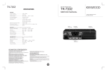
TK-280
SERVICE MANUAL
© 1999-4 PRINTED IN JAPAN
B51-8454-10(S) 1217
REVISED
This service manual is same at the TK-280(B51-8454-00)
service manual with destination K, K3 and M with the
exception of new destination, K2 and K4.
CONTENTS
Helical antenna
(T90-0679-05):M
GENERAL ................................................................................. 2
Knob (ENC)
(K29-5232-03)
OPERATING FEATURES ......................................................... 3
SYSTEM SET-UP ..................................................................... 2
REALIGNMENT ...................................................................... 11
CIRCUIT DESCRIPTION ........................................................ 16
Knob (VOL)
(K29-5231-03)
SEMICONDUCTOR DATA ..................................................... 22
DESCRIPTION OF COMPONENTS ....................................... 27
PARTS LIST ............................................................................ 28
Panel assy
(A62-0535-04)
Badge
(B43-1106-14)
EXPLODED VIEW .................................................................. 34
PACKING ................................................................................ 35
ADJUSTMENT ........................................................................ 36
TERMINAL FUNCTION .......................................................... 44
PC BOARD VIEWS
Knob (PTT etc)
(K29-5157-03)
Cabinet assy
DISPLAY UNIT (X54-3210-XX) ........................................... 45
(A02-2054-53)
TX-RX UNIT (X57-5740-XX) ............................................... 51
:K,K2,M (4 keys)
(A02-2055-53)
SCHEMATIC DIAGRAM ......................................................... 57
:K3,K4 (16 keys)
BLOCK DIAGRAM .................................................................. 61
LEVEL DIAGRAM ................................................................... 63
OPTINONS ............................................................................. 64
SPECIFICATIONS ............................................... BACK COVER
Packing
(G53-0840-02):K,K2,M (4 keys)
(G53-0841-02):K3,K4 (16 keys)
Photo is K3 type with KRA-14
CAUTION
When using an external power connector,
please use with maximum final module
protection of 9V.
TK-280
GENERAL / SYSTEM SET-UP
●
INTRODUCTION
SCOPE OF THIS MANUAL
●
This manual is intended for use by experienced technicians
familiar with similar types of commercial grade communications
equipment. It contains all required service information for the
equipment and is current as of the publication data. Changes
which may occur after publication are covered by either Service
Bulletins or Manual Revisions. These are issued as required.
SHUT OFF and DO NOT operate this equipment near
electrical blasting caps or in an explosive atmosphere.
This equipment should be serviced by a qualified technician
only.
SERVICE
This radio is designed for easy servicing. Refer to the
schematic diagrams, printed circuit board views, and alignment
procedures contained within.
ORDERING REPLACEMENT PARTS
NOTE
When ordering replacement parts or equipment information,
the full part identification number should be included. This
applies to all parts : components, kits, or chassis. If the part
number is not known, include the chassis or kit number of which
it is a part, and a sufficient description of the required
component for proper identification.
WE CANNOT guarantee oscillator stability when using
channel element manufactured by other than KENWOOD or
its authorized agents.
FCC COMPLIANCE AND TYPE NUMBERS
Type Type acceptance number Frequency range
K,K3 ALH24613110
146~174MHz
K2,K4 ALH24613120
136~162MHz
PERSONNEL SAFETY
The following precautions are recommended for personnel
safety:
● DO NOT transmit until all RF connectors are verified secure
and any open connectors are properly terminated.
Unit
Model &
destination
K, M
K3
TK-280
K2
K4
X57-5740-XX X54-3210-XX
0-10
_
_
0-11
0-10
_
Frequency range
QT/DQT DTMF
Charger Battery 16 Keys
0-11
_
_
_
Remarks
Compliance
Parts 22,74,80,90
Parts 22,74,80,90
_
_
146~174MHz
136~162MHz
IF1 : 44.85MHz
LOC : 44.395MHz
_
_
–
_
–
_
OP
OP
OP
OP
SYSTEM SET-UP
Merchandise received
License and frequency allocated by FCC
Frequency range (MHz) RF power
Choose the type of transceiver
Transceiver programming
Are you using the speaker microphone?
NO
Delivery
2
Type
TX/RX 146~174
TK-280 K,K3,M
5.0W
TX/RX 136~162
TK-280 K2,K4
A personal computer (IBM PC or compatible), programming
interface (KPG-36), and programming software (KPG-49D)
are required for programming.
(The frequency, trunked system features, conventional system
features, TX power HI/LOW, and signalling data are programmed
for the transceiver.)
YES
KMC-25
Speaker microphone
(Option)
–
_
–
_
TK-280
OPERATING FEATURES
1. Operation Features
The TK-280 is an VHF FM radio designed to operate in
both trunking format and conventional format. The
programmable features are summarized.
Model
Trunking Format
Conventional Format
Trunking mode
Conventional mode
■ Trunking Format
This format can handle up to 32 systems with up to 250
groups in each system. The transceiver can be used in both
trunked mode and conventional mode. Systems, groups,
and their functions are programmed.
■ Conventional Format
This format can handle up to 250 groups with 250 channels
in each group.
The transceiver can be used only in conventional mode.
Groups, channels, and their functions are programmed.
2. Transceiver Controls and Indicators
2-1. Physical Layout
●
lowest system number (or group number).
System numbers (or group numbers) not set are skipped.
Caution : The FPU (KPG-49D) allows selecting between
system selector and group selector.
Conventional Format
Turning the group (or channel) selector knob clockwise
increases the group (or channel) number by one. Turning
the knob in the counterclockwise direction decreases the
group (or channel) number by one.
After the group number (or channel number) reaches the
highest group number (or channel number), it goes back to
lowest group number (or channel number).
Group numbers (or channel numbers) not set are skipped.
Caution : The FPU (KPG-49D) allows selecting between
group selector and channel selector.
3 Volume/Power switch
● Trunking Format
Transceiver Power and Volume switch. Turn clockwise to
switch On the transceiver. Turn counterclockwise fully to
switch OFF the transceiver. Also adjusts the volume level.
When the power is switched off, all the parameters, such
as the system and group, are stored in memory. When the
power is switched on again, the system returns to the
previous conditions.
● Conventional Format
Transceiver Power and Volume switch. Turn clockwise to
switch On the transceiver. Turn counterclockwise fully to
switch OFF the transceiver. Also adjusts the volume level.
When the power is switched off, all the parameters, such
as the group and channel, are stored in memory. When the
power is switched on again, the group returns to the previous
conditions.
4 Auxiliary (orange) key (Programmable)
Note: The transceiver is also available without the DTMF
keypad (-).
5 Battery pack release catch
Push down to release the battery pack. See Installing the
Ni-Cd Battery Pack.
2-2. Panel controls
6 MONITOR key* (Programmable)
The key on the top and front panel is momentary-type push
buttons. The functions of these keys and knob are explained
below.
7 PTT (Push-To-Talk) key
Press this key, then speak into the microphone to call a
station.
1 Antenna connector
Connect the supplied antenna here.
2 System or Group selector knob (Programmable)
●
Trunking Format
Turning the system (or group) selector knob clockwise
increases the system (or group) number by one. Turning
the knob in the counterclockwise direction decreases the
system (or group) number by one.
After the system number (or group number) reaches the
highest system number (or group number), it goes back to
8 LAMP key* (Programmable)
9 TX/BATT indicator
This red LED lights during transmission (it does not light
during busy or when transmit is prohibited). If the battery
voltage falls below the programmed voltage during
transmission, the brightness of this indicator decreases at
intervals of about one second, so it can be used as the
battery voltage alert function.
3
TK-280
OPERATING FEATURES
0 S, A, 2 B, and C 3 key (Programmable)
- DTMF keypad (keypad model only)
Press the keys on the telephone keypad to send DTMF
tones.
the underscore disappears and the AUX ports turns to the
deactive level.
= Universal connector
Connect the external KMC-25 speaker/ microphone
(optional) here. Otherwise, keep the supplied cover in place.
3) Channel up/down (Conventional Format)
When the key is pressed each time, the channel number to
be selected is incremented/decremented and repeats if held
for one second or longer.
This key works as the voice scrambler code selector in the
voice scrambler code select mode.
* : MONITOR and LAMP are arbitrary names chosen for
these buttons. They can be used for any of the auxiliary
functions.
4) Connect ID
Pressing this key in Conventional mode, automatically sends
the preset Connect ID.
2-3. Programmable keys
The FPU (KPG-49D) enables programmable keys to select
the following functions.
■ Trunking Format
Auto Tel, AUX(only when Voice Scrambler is not selected),
Connect ID, Disconnect ID, Display Character, Emergency
(only AUX key), Function, Group Down, Group Up, Home
Group, Key Lock, Lamp, Memory (RCL/STO), Memory (RCL),
Memory (STO), Monitor A, Monitor B, Monitor C, Monitor D,
Redial, RF Power Lo, Scan, Scan Del/Add, Scan Temporary
Delete, Scrambler (Only when Voice Scrambler is selected),
System Down, System Up, TEL Disconnect and none.
5) Disconnect ID
Pressing this key in Conventional mode, automatically sends
the preset Disconnect ID.
6) Display character
● Trunking Format
This key switches the LCD display between the system/
group number and system/group name.
● Conventinal Format
This key switches the LCD display between the group/
channel number and group/channel name.
1) Auto TEL (Trunking Format)
Automatically connects available repeaters that are
connected to telephone circuits when operating as LTR
system. The time allocated to search for available repeaters
is 60 seconds, after which connection failure occurs, a DTMF
tone is output and the function terminates.
If connection to an available circuit is made, only ID 253,
EOT or hang-up time-out can terminate the function.
7) Emergency
Trunking Format
Pressing this key for longer than the programmed
“Emergency Key Delay Time” causes the transceiver to enter
the emergency mode. The transceiver jumps to the
programmed “Emergency System/Group” and transmits for
the programmed “Active Time”.
The transceiver disables mic mute while transmitting. After
finishing transmission, the transceiver receivers for the
programmed “Interval Time”. The transceiver mutes the
speaker while receiving. Following the above sequence, the
transceiver continues to transmit and receive.
● Conventinal Format
Pressing this key for longer than the programmed
“Emergency Key Delay Time” causes the transceiver to enter
the emergency mode. The transceiver jumps to the
programmed “Emergency Group/Channel” and transmits for
the programmed “Active Time”.
The transceiver disables mic mute while transmitting. After
finishing transmission, the transceiver receivers for the
programmed “Interval Time”. The transceiver mutes the
speaker while receiving. Following the above sequence, the
transceiver continues to transmit and receive.
2) AUX
This function can be programmed when the voice scrambler
board is not installed.
If this key is pressed, an underscore (“_”) appears at the
extreme right of the LCD and AUX port which is inside of
the transceiver turns to the active level. If pressed again,
8) Function
Pressing this key causes the transceiver to display “FCN”.
Then, pressing a DTMF key causes the corresponding
programmed function to start. This key may be convenient
when using many functions with the 12-key keypad (K3, K4
type).
●
■ Conventional Format
AUX(only when Voice Scrambler is not selected), Channel
Down, Channel UP, Connect ID, Disconnect ID, Display
Character, Emergency (only AUX key), Function, Group Down,
Group Up, Home Channel, Key Lock, Lamp, Memory (RCL/
STO), Memory (RCL), Memory (STO), Monitor A, Monitor B,
Monitor C, Monitor D, Operator Selectable Tone, Redial, RF
Power Lo, Scan, Scan Del/Add, Scrambler (Only when Voice
Scrambler is selected), Talk Around and none.
These functions the FPU programs to the function keys are
described in the following sections.
4
TK-280
OPERATING FEATURES
9) Group up/down
When the key is pressed each time, the group number to
be selected is incremented/decremented and repeats if held
for one second or longer. In Conventional format, this key
works as the voice scrambler code selector in the voice
scrambler code select mode.
10) Home Channel (Conventional Format)
Press this key once, the channel switches to the preprogrammed home channel.
11) Home group (Trunking Format)
Each pressing of the key selects a preset system/group.
12) Key lock
Pressing this key causes the transceiver to accept entry of
only the [Function], [Key Lock], [PTT], [Lamp], [Monitor A],
[Monitor B], [Monitor C], [Monitor D], and [Emergency] keys.
The locked keys also include the tuning control.
13) Lamp
This key illuminates the LCD and keys on the front panel.
When the key is pressed, the LED lamp goes on.
When it is released, the lamp goes off after about five
seconds. If any key is pressed while the LED lamp is on,
the lamp is kept on for five seconds.
14) Memory
This key allows DTMF memory data to be recalled; up to 32
memories each with a memory dial of up to 16 digits
and an A/N of up to 10 digits per memory.
15) Monitor
Used to release signalling or squelch when operating as a
conventional. It is also used to reset option signalling.
16) Operator Selectable Tone (Conventional Format)
This key switches the pre-set decode QT/DQT and encode
QT/DQT to OST (Operator Selectable Tone) tone pair.
Press this key, the transceiver enters to OST select mode.
In this mode, the display shows “OFF” and the operator can
select one of the OST tone pair using the tuning control.
The display shows “TONE ∗∗” and tone pair No. ∗∗ is
selected.
Press OST key again, the transceiver exits from the OST
select mode, and returns to the group/channel mode with
the handset indicator ( ) means that the OST tone pair is
selected. OST tone pair number or OFF can be memorized
for each channel.
16 kinds of tone pair for OST can be programmed by KPG49D. OST is useful to access the repeater with same radio
frequency and different tone (QT/DQT).
17) Redial
Pressing this key when System/Group(trunking format),
Group/Channel (Conventional Format) is shown, displays the
previously transmitted DTMF code. Pressing [PTT] at this time,
transmits the code that is currently displayed.
18) RF power low
Used to temporarily switch transmission output to low power.
Turning the function on enables:
Hi→Low, Low→Low
Key states are backed up, except in the PC mode when
they are reset.
19) Scan
Press this key starts scanning. Pressing this key stops
scanning.
20) Scan Del/Add
● Trunking Format
Used to select whether system scan routines are used during
system scan. Each pressing of the key (to ON) toggles
between lockout and lock. The scan routine is started when
on lock. The DEL indicator flashes when the system is on
lockout.
● Conventinal Format
This key switches the currently displayed channel between
“Delete” and “Add”.
The “Add” channel contained in the scan sequence, and
“Delete” channel is not contained. In the scan mode, this
key switches the channel delete or add temporarily.
21) Scan temporary delete (Trunking Format)
This key is temporarily deleted a system being scanned. If
you press this key when scan is stopped (when a call is
being received from another station), the system is
temporarily deleted and scanning restarts.
This key operates even when “Scan Type” is set to “List
Type System Scan”.
22) Scrambler
If a scrambler code (1 to 4) has been set in the FPU, an
underscore (“_”) appears at the extreme right of the LCD
display when scrambler is active. Pressing this key changes
ON/OFF of scramble operation.
Holding this key down for 2 seconds sets Scramble Code
Select Mode
23) System up/down (Trunking Format)
When the key is pressed each time, the system number to
be selected is incremented/decremented and repeats if held
for one second or longer.
24) Talk Around (Conventional Format)
Press this key, the transceiver uses the receive frequency
and the tone for transmission.
The operator can call the other party directory (without
repeater). Press this key again, the talk around function goes
off.
5
TK-280
OPERATING FEATURES
25) Telephone disconnect (Trunking Format)
Pressing this key ends an RIC connection (disconnects the
telephone line).
26) None
Sounds error operation beep, and no action will occur.
Use this function when the transceiver is required to be more
simple operated.
●
2-4. Display
P
or scrambler ( _ ) function. The delete/add indicator shows
the systems locked out of the scanning sequence. Selective
call and scrambler are optional functions that can be
programmed.
Conventinal Format
The twelve-character dot matrix alphanumeric display
shows the group and channel numbers. You can program
group and channel names with up to ten characters in place
of these numbers. The left display is used as an add
indicator (∞) and the right is used for the selective call (:+:)
or scrambler ( _ ) function. The add indicator shows the
channels unlocked out of the scanning sequence. Selective
call and scrambler are optional functions that can be
programmed.
3. Scan Operating
9
1 Sub display
Displays the system, channel and group numbers. Also
displays various functions, such as TA.
2 P (Priority) indicator
The P indicator ( P ) appears when a selected channel is
programmed as priority, in conventional operation.
3 MON (Monitor) indicator
The MON indicator appears when the button programmed
as MONITOR is pressed.
4 SVC (Service) indicator
This icon is not used on this transceiver.
5 SCN (Scan) indicator
The SCN indicator appears when using Scan mode.
3-1. In Case of Trunking Format
1) System scan
System scan can be selected with the “Scan” key by
programming the scan feature. When the “Scan” key is pressed
and the “SCN”’ mark appears, scan mode in entered. Scanning
starts from the system following the currently displayed system.
When a call is received, scanning stops, and the system and
group are displayed.
When the system knob or programming key is touched
during scanning, the scan stops and the revert system or group
can be changed. Scanning resumes one second after the key
is released.
System Scan consists of the following 2 types.
● Fix system scan
All the set systems except locked-out ones are scanned. If
the DEL/ADD feature is assigned to the programmable key, it
can be controlled from the front panel.
List type system scan
A scan list can be set for each system.
The list to be scanned can be changed by changing the
display system
If many system have been set, the scan speed can be
increased by narrowing the systems to be scanned with scan
lists.
●
6 LO indicator
Appears when low power is selected.
7 Handset indicator
The handset indicator ( ) appears when the selected group
is programmed as telephone IDs. (Trunking Format) In
Conventional Format, the handset indicator ( ) appears
when the OST tone pair is selected.
8 MAIL indicator
This icon is not used on this transceiver.
9 Alphanumeric display
● Trunking Format
The twelve-character dot matrix alphanumeric display
shows the system and group numbers. You can program
system and group names with up to ten characters in place
of these numbers. The left display is used as a delete
indicator (3) and the right is used for the selective call (:+:)
6
2) System lockout
The system lockout feature is used to lock systems out of
the scan sequence, and can be selected by programming in
the following two ways:
Fixed lockout
The system to be locked out is selected by programming.
When a locked system is selected, the Delete (3) indicator
appears on the left of the SYSTEM indicator. The revert system
is scanned even if it is locked out. If there is a locked system,
the Delete (3) indicator flashes during fixed scanning.
●
TK-280
OPERATING FEATURES
User selectable lockout
If the scan lockout feature is programmed to a key, the user
can lock systems out of the scan sequence with the key. To
lock a system out of the scan sequence, press the key when
the system is displayed. The Delete (3) indicator is displayed
on the left of the SYSTEM indicator.
To unlock a system, select the system and press the key.
The Delete (3) indicator disappears to indicate that the system
has returned to the scan sequence. The revert system is
scanned even if it is locked out. If there a locked system, the
Delete (3) indicator flashes during fixed scanning. If all systems
are locked out, the scan stops and only the revert system is
received.
●
3) Drop-out delay time (Scan resume time)
If a call is received during scan, the scan stops. The scan
resume time can be programmed as 0 to 300 seconds in onesecond increments. The default value is 3 seconds.
4) Dwell time
The dwell time is the time after transmission ends until the
scan resumes in scan mode. It can be set 0 to 300 seconds by
programming. The default value is 3 seconds.
5) System/Group revert
System/Group revert can be programmed for one of the
following;
Last called revert
The system or group changes to the revert system or group
when a call is received with the system or group being scanned.
7) Group scan operation
Group scan can be programmed for each group. In addition
to the ID codes of the selected group, the ID codes of the
other groups that are permitted for group scan are decoded.
(The two fixed ID and block decode codes are always decoded.)
If, during group scanning, a call is received with one of the
selectable group ID codes for which group scan is enabled,
the group display indicates the group number that the call came
in with. That group then becomes the new selected group.
Group scan resumes after the specified dropout delay time or
dwell time shared by the system scan elapses.
8) In Conventional system.
If QT or DQT is set for the channel, the channels, including
signalling, are scanned.
In case of the priority group is set in conventional system, if
a group scan (including group scan during a system scan)
temporarily stops (receiving) in a group that does not have
priority, a look back is performed to the priority group. Look
back is performed according to the look back time A and B
settings. If a call is received on the priority group, reception
immediately switches to the priority group.
3-2. In Case of Conventional Format
1) Scan types
Single Group Scan
You can scan all valid (ADD) channels in the displayed group
that can be selected with the group selector.
●
●
Last used revert
If a system/group call is received during scanning and the
PTT button is pressed for transmission and response within
the drop out delay time, the system or group is assigned as
the new revert system or group.
Multiple Group Scan
You can scan all valid (ADD) channels in the all valid (ADD)
group.
●
●
2) Scan Start Condition
Selected revert
If the system/group was changed while scanning, the newly
selected system/group.
One or more non-priority channels must be added to all
channels that can be scanned. The transceiver must be in
normal receive mode (PTT off).
When you activate the key programmed to the scan function,
the scan starts. The scan icon “SCN” lights and “-SCAN-” or
revert channel (programmable) is indicated on alphanumeric
display.
6) Scan message wait
3) Scan Stop Condition
The time for staying with the home repeater that receives a
signal during system scan and monitoring data messages can
be programmed. If there is no signal from the home repeater,
the system is scanned for about 50ms. If there is a signal,
three data messages are monitored. Normally, three data
messages are monitored for each system, and it can be
increased in multiples of three data messages per line to up to
eight lines.
If the repeater data message indicates that there is no call,
data monitoring is terminated and the home repeater of the
next system is scanned.
The scan stops temporarily if the following conditions are
satisfied.
1 A carrier is detected, then signalling matches on channels
for which receive the signalling is set by the programming
software.
2 A carrier is detected on the channel for which receiving
signalling is not set by the programming software or when
the monitor (signalling cancel) function is activated.
●
4) Scan Channel Types
1 Priority channel is the most important channel for the scan,
and always detects a signal during scan and when the scan
stops temporarily.
7
TK-280
OPERATING FEATURES
2 Non-priority channels detects a signal during scan. For the
channels that can be selected with the group or channel
selector when the scan does not occur, adds an indicator
“∞” lights.
5) Priority Channel Setting
A priority channel can be set as follows with the programming
software (KPG-49D).
1 Specify a priority channel as a fixed priority channel.
2 Make a selected channel a priority channel.
6) Scan Type According to the Priority Channel
1 When no priority channel is set : Only the non-priority
channels are scanned.
If a non-priority channel stops temporarily, it stops until
there is no signal on the channel.
2 When priority channel is set : Either priority channel is
scanned.
If a non-priority channel stops temporarily, a priority channel
signal is detected at certain intervals.
If a priority channel stops temporarily, it stops until there is
no signal on the priority channel.
7) Revert Channel
The revert channel is used to transmit during scanning and
set by the programming software (KPG-49D).
1 Priority
The transceiver reverts to the priority channel
2 Priority with talkback
The transceiver reverts to the priority channel.
If you press PTT during a resume timer (dropout delay time,
TX dwell time) or calling, you can transmit on current
channel to answer to the call however revert channel is set
to priority channel.
After resume time, scan re-starts and transmission channel
is return to priority channel.
3 Selected channel
The transceiver reverts to the channel before scanning or
the channel that you changed during scan.
4 Last called channel
The transceiver reverts to the last called channel during
the scan.
5 Last used channel
The transceiver reverts to the last used (transmitted)
channel during scan. “Last used” revert channel includes
talkback function.
6 Selected with talkback
The transceiver reverts to the channel before scanning or
the channel that you changed during scan.
8) Scan End
When you reactivate the key programmed to the scan
function during scan mode, the scan ends.
The scan icon “SCN” and “-SCAN-” or revert channel
(programmable) display goes off.
8
9) Temporarily Delete/Add
It is possible to delete or add channel temporarily during
scan. When scan stops on unnecessary channel for example
by interference of the other party, activate the delete/add
function (for example press the key), then that channel is
deleted temporarily and scan re-start immediately.
When you would like to add the deleted channel temporarily
to scan sequence, select the desired (deleted) channel during
scan, activate the delete/add function (for example press the
key) before scan re-start.
That channel is added temporarily to scan sequence. The
temporary deleted or added channels are returns to pre-set
delete/add, when the transceiver exits from scan mode.
4. Details of Features
4-1. In Case of Trunking Format/Conventional Format
1) Time-out timer
The time-out timer can be programmed in 15 seconds
increments from 15 seconds to ten minutes. If the transmitter
is keyed continuously for longer than the programmed time,
the transmitter is disabled and a warning tone sounds while
the PTT button is held down. The alert tone stops when the
PTT button is released.
2) Sub LCD
You can use 3-digit the display to display the system number,
channel number or group number. It is useful when the main
(12-digit) display indicates system, group or channel name or
other functions.
3) Selective Call Alert LED
You can select whether or not the LED on the transceiver
flashes in an orange color when selective call was occurred.
4) PTT ID
PTT ID provides a DTMF ANI to be sent with every time
PTT (connect ID at beginning of transmission, disconnect ID
at end of transmission, or both).
You can program PTT ID "on" or "off" for each group
channel. The contents of ID are programmed for each
transceiver.
The transceiver is capable to have ID. The format is DTMF.
The timing that the transceiver sends ID is programmable.
Connect ID : Connect ID is sent on beginning of transmission.
Disconnect ID : Disconnect ID is sent on end of transmission.
Both : Connect ID is sent on beginning of transmission and
disconnect ID is sent on end of transmission.
There is also "PTT ID" setting for each channel.
5) Radio password
When the password is set in the transceiver, user can not
use the transceiver unless enter the correct password.
This code can be up to 6 digits from 0 to 9 and input with
the keypad or selector, and “S” key.
TK-280
OPERATING FEATURES
6) Battery Warning
This transceiver has battery warning feature. If the low
voltage is detected during transmission, the transceiver warns
it by flashing red "LED".
Then more low voltage is detected during transmission, the
transceiver stops transmission and warns it by flashing red
"LED" and beep.
Please notice "standard" for the battery exchange, charging
time by flashing red LED and beep.
selected system (If during scanning, the scan stops).
4) Transpond
This feature can be programmed to turn on and off for each
group. If the ID of the group for which transpond is enabled is
received, two data messages (transmit ID and turn-off code)
are automatically transmitted if the PTT button is not pressed
as a response within the time set (0 to 300 seconds in 1-second
increments). If the PTT button is pressed within the time, the
transpond is not preformed.
7) Minimum Volume
The minimum volume is programmable (off (0) to 31). The
transceiver remains the minimum volume level however the
mechanical volume position is set to zero.
4-2. In Case of Trunking Format
1) Call indicator
The call indicator can be programmed for each group. In
trunked system, it can be set to respond to a selectable decode
ID or one of two fixed IDs, except block IDs. When a call is
received with a selectable decode ID, the call indicator flashes.
When a call is received with a fixed ID, the call indicator lights
continuously.
On a conventional system, the call indicator can be
programmed to light for each QT or DQT code. It keeps flashing
while a call is being received. It is turned off by pressing any
front panel key.
2) Free system ringback
This feature is available only when a telephone
interconnected ID code is selected. If a busy tone sounds when
the PTT button is pressed, the transceiver enters this mode
automatically.
When the PTT button is released, a beep sounds for 400ms
to indicate that the mode has been entered. If the scan is on, it
is resumed (the “SCN” mark goes on). When any repeater
becomes available, a ringing tone sounds and this mode ends.
The mode is terminated when the system, group, scan, PTT,
key is changed.
3) System search
This feature can be programmed to automatically access
other programmed systems when the selected system cannot
be accessed. If an intercept tone sounds when the PTT button
is pressed after setting the mode, the transceiver has entered
the mode.
If the group ID is a telephone interconnect ID, the transceiver
then attempts to access, in succession, other systems that
have a telephone interconnect ID in the revert group location.
If the group ID is a dispatch ID, the transceiver attempts to
access other systems that have a dispatch ID programmed in
the revert group location.
If there is no system to be accessed, an intercept tone
sounds, the mode is terminated, and the transceiver returns to
the first system. If the access is successful, the mode is
terminated, and the searched system becomes the new
5) Transmit inhibit
The transceiver can be programmed with a transmit inhibit
block of ID codes. If an ID code within this block is decoded
the preset time before the PTT button is pressed, transmission
is inhibited. The BUSY indicator lights and a busy tone sounds
until the PTT button is released to indicate that transmission is
not possible (except clear-to talk mode).
Transmission with the group for which the encode ID is not
set is inhibited, and the busy tone is output while the PTT button
is held down, regardless of the clear-to -talk setting.
6) Auto TEL
A telephone interconnect call can be made by simply
pressing the key by assigning this feature to the key. This
feature accesses the TEL channel of the available system
automatically.
When the key is pressed, a queue tone is output, and the
“AUTO TEL” appears on the alphanumeric display along with
a flashing handset indicator ( ) to indicate that this mode has
been entered. If the TEL ID is set for the revert system, the
TEL channel of that system is accessed. If all TEL channels
are busy, an attempt is made to access the TEL channels of
another system in which the TEL ID code has been programmed. It is repeated for 60 seconds until the access
succeeds. If the access succeeds, a dial tone returns from the
repeater. If the key is pressed again when the queue tone is
sounding, this mode is canceled.
If the access fails after 60 seconds, a deny tone is output
and this mode is terminated. When the talk ends, the revert
system/group returns. When the scan mode is effective, the
scan resumes. The Auto TEL feature can be programmed to
turn on or off for each system.
4-3. In Case of Conventional Format
1) "TOT" Pre-Alert
The transceiver has "TOT" pre-alert timer. This parameter
selects the time at which the transceiver generates "TOT" prealert tone before "TOT" is expired.
"TOT" will be expired when the selected time passes from
a TOT pre-alert tone.
2) "TOT" Re-Key Time
The transceiver has "TOT" re-key timer. This timer is the
time you can not transmit after "TOT" exceeded. After "TOT"
re-key time expired you can transmit again.
9
TK-280
OPERATING FEATURES
3) "TOT" Reset Time
The transceiver has "TOT" reset timer. This timer is the
minimum wait time allowed during a transmission that will reset
the "TOT" count.
"TOT" reset time causes the "TOT" to continue even after
PTT is released unless the "TOT" reset timer has expired.
4) OST (Operator Selectable Tone)
The transceiver is capable to have "OST" function and 16
tone pair (QT/DQT) with max 10-digit name for each tone pair.
• "OST" Back Up
The transceiver is programmable the selected "OST" code
is memorized or not. If you set to Disable (no memorized), the
"OST" function always starts at "off".
• Direct "OST"
It is possible to call "OST" number directory using keypad.
In this case, keypad is used for "OST", then "Auto PTT" "Store
& Send" functions by keypad are not usable.
5) Clear to Transpond
The transceiver waits the transpond of 2-Tone/DTMF if
channel is busy until channel open. This feature prevents the
interference to other party.
6) Battery Save
This is the automatic battery saver during a standby mode
operation. The receiver circuit is repeated on and off to
conserve the battery life.
AND
OR
Alert/Transpond
Triggers at match with QT/
DQT/ID+DTMF(2tone);Both
LTR Format→ Triggers at
match with QT/DQT/ID+DTMF
:Both
Conventional Format →
Triggers only for match with
DTMF (2tone) : Opt
AF Mute Open
Triggers at match with QT/
DQT/ID+DTMF(2tone);Both
Triggers only for match with
QT/DQT/ID;Signaling
Even if set for OR, AF mute cannot be canceled just by a
match with DTMF.
In conventional channels not set with QT/DQT, signaling is
a match just by receiving the carrier.
Auto Reset
When Option Signaling matches on a Group channel where
set to Yes, Option Signaling is canceled when it matches a
group channel set to Yes.
After Option Signaling is a match, Option Signaling can
automatically set to Reset after a specified time.
Dead Beat Disable
When the D.B.D (Dead Beat Disable) code is a match, a
preset operation is performed.
When D.B.D matches on all group channels regardless of
whether Option Signaling = Yes/No, then TX Inhibit or TX RX
Inhibit is activated by settings performed afterwards. D.B.D is
canceled when the D.B.D. code + “#” is received.
Transpond is always activated when the D.B.D code is a
match. Alert is not output. An Option Signaling match is not
displayed.
5. Option Signalling (DTMF/2 tone)
Built-in DTMF decoder is available for option signalling.
Built-in 2-Tone decoder is available for option signalling.
It is possible to use individual call, group call, DBD (Dead
Beat Disable). Note : DBD is only DTMF.
Preset operation is triggered when matches with Option
Signaling
When Option Signaling matches on a Group Channel where
set to Yes, the Option Signaling display flashes and Option
Signaling is canceled. Settings after this will cause “Transpond”
or “Alert” to sound.
Setting the Selective Call Alert LED will make an orange
LED start flashing.
Mute or Unmute is triggered by the ID/QT/DQT/Carrier when
option signaling is a match (when Option Signal is deactivated
by a transmission).
AND/OR
Option Signaling match conditions can be selected with
AND/OR logic.
10
6. Audible user feedback tones
The transceiver outputs various combinations of tones to
notify the user of the transceiver operating state. The main
tones are listed below
The high tone is 1477Hz, the mid tone is 941Hz, and the
low tone is 770Hz.
• Power on tone
This tone is output when the transceiver is turned on. (The
high tone is output for 500ms.)
• Alert tone
This tone is output when the transceiver is TX inhibition for
TOT, battery warning and PLL unlocked. It is output until the
PTT button is released. (The 697Hz tone is output.)
• Busy Tone
In trunked mode (of trunking format) the busy tone informs
the user when the repeater cannot be used (System busy or
TX inhibit status).
In conventional mode (of conventional format), this informs
the user of a Busy Channel Lockout.
TK-280
OPERATING FEATURES/REALIGNMENT
•
Group Call Tone
The group call tone informs the user of a group call in DTMF/
2Tone Option Signaling. This tone repeats 7 times.
770Hz
770Hz
30ms
30ms
30ms
• Individual Tone
Individual tone is issued on receiving selective call by DTMF/
2 Tone Option Signaling.
2000Hz
100ms
100ms
2000Hz
100ms
100ms
2000Hz
100ms
• Ringing tone (Trunking Format)
This tone indicates that the transceiver can use the repeater
in free system ringback mode. (The mid tone and no tone are
output eight cycles alternately in 50ms intervals.)
• Pre Alert tone (Conventional Format)
Informs user when nearing transmit inhibit (transmit cutoff)
time due to TOT.
The Pre Alert Tone is issued from the time set for TOT Pre
Alert until the TOT triggers.
1633Hz
50ms
50ms
1633Hz
50ms
50ms
1633Hz
50ms
• Intercept tone (Trunking Format)
This tone indicates that the transceiver is out of range. It
indicates that the PTT button is pressed, and transmission has
started, but the repeater cannot be connected and talking is
not possible. It is output until the PTT button is released. (The
mid tone and low tone are output alternately in 200ms intervals.)
• Delay tone (Trunking Format)
This tone is output when the PTT button is pressed and the
repeater is accessed three times or more to indicate connection
with the repeater is delayed. This tone is the same as the busy
tone. (It is not output of CLEAT TO TALK has been set to
YES.)
• Proceed tone (Trunking Format)
This tone is output when the PTT button is pressed,
transmission starts, and the repeater is connected to indicate
that the user can talk if the Clear-to-talk function has been set.
(The high tone is output for 100ms.)
REALIGNMENT
1. Modes
User mode
Panel test mode
Panel tuning mode
PC mode
Data programming
mode
Firmware
programming mode
PC test mode
PC tuning mode
Clone mode
• Queue tone (Trunking Format)
This tone is output until the Auto TEL function is set and the
TEL channel is accepted successfully. (The mid tone on for
50ms, off for 50ms, and on for 50ms in 1 second intervals.)
• Deny tone (Trunking Format)
This tone is output if the Auto TEL function is set, the queue
tone is output, but the TEL channel cannot be accessed within
60 seconds. It is similar to the intercept tone. (The mid tone
and low tone are output alternately in 150ms intervals.)
• Free system ringback mode tone, system search mode
tone (Trunking Format)
This tone indicates that the transceiver is free system
ringback mode or system search mode. (The low tone is output
for 400ms.)
Self programming
mode (Conventional
Format)
Mode
User mode
Panel test mode
Panel tuning mode
PC mode
Data programming mode
PC test mode
Firmware programming mode
Clone mode
Self programming
mode (Conventional
Format)
Function
For normal use.
Used by the dealer to check the
fundamental characteristics.
Used by the dealer to tune the radio.
Used for communication between the
radio and PC (IBM compatible).
Used to read and write frequency data
and other features to and from the radio.
Used to check the radio using the PC.
This feature is included in the FPU.
See panel tuning.
Used when changing the main
program of the flash memory.
Used to transfer programming data
from one radio to another.
Frequency, signalling and features
write to the radio.
11
TK-280
REALIGNMENT
2. How to Enter Each Mode
Mode
User mode
Panel test mode
PC mode
Panel tuning mode
Firmware programming mode
Clone mode
Self programming mode
(Conventional Format)
Operation
Power ON
[A]+Power ON (Two seconds)
Received commands from PC
[Panel test mode]+[S]
[S]+Power ON (Two seconds)
[C]+Power ON (Two seconds)
[LAMP]+Power ON
(Two seconds)
5-5. Programming with IBM PC
If data is transferred to the transceiver from an IBM PC with
the KPG-49D, the destination data (basic radio information)
for each set can be modified. Normally, it is not necessary to
modify the destination data because their values are
determined automatically when the frequency range (frequency
type) is set.
The values should be modified only if necessary. Data can
be programmed into the flash memory in RS-232C format via
the universal connector.
KPG-49D instruction manual parts No. : B62-1096-XX
3. Panel Test Mode
Setting method refer to ADJUSTMENT.
4. Panel Tuning Mode
Setting method refer to ADJUSTMENT.
5.PC Mode
5-1. Preface
The TK-280 transceiver is programmed by using a personal
computer, programming interface (KPG-36) and programming
software (KPG-49D).
The programming software can be used with an IBM PC or
compatible. Figure 1 shows the setup of an IBM PC for
programming.
5-2. Connection procedure
1. Connect the TK-280 to the personal computer with the
interface cable.
2. When the POWER switch on, user mode can be entered
immediately. When PC sends command the radio enter PC
mode, and “PROGRAM” is displayed on the LCD.
When data transmitting from transceiver, the red LED is
blinking.
When data receiving to transceiver, the green LED is blinking.
Notes:
• The data stored in the personal computer must match model
type, when it is written into the flash memory.
• Change the TK-280 to PC mode, then attach the interface
cable.
5-3. KPG-36 description
(PC programming interface cable: Option)
The KPG-36 is required to interface the TK-280 to the
computer. It has a circuit in its D-subconnector (25-pin) case
that converts the RS-232C logic level to the TTL level.
The KPG-36 connects the universal connector of the TK280 to the computers RS-232C serial port.
5-4. Programming software description
12
The KPG-49D programming disk is supplied in 3-1/2” disk
format. The software on this disk allows a user to program TK280 radios via programming interface cable (KPG-36).
KPG-49D
Fig. 1
6. Firmware Programming Mode
6-1. Preface
Flash memory is mounted on the TK-280. This allows the
TK-280 to be upgraded when new features are released in the
future. (For details on how to obtain the firmware, contact
Customer Service.)
6-2. Connection procedure
Connect the TK-280 to the personal computer (IBM PC or
compatible) with the interface cable (KPG-36). (Connection is
the same as in the PC Mode.)
6-3. Programming
1. Start up the programming software (KPG-49D), select
"firmware program" in the "Program" item, and press the
Return key on the personal computer. This starts up the
firmware programmer.
2. The top screen is displayed. Press any key to advance to
the next screen.
3. Set the communications speed (normally, 57600 bps) and
communications port in the Setup item.
4. Set the firmware to be updated by File select (=F1).
5. Turn the TK-280 power ON with the [S] switch held down.
Hold the switch down for two seconds until the display
changes to "PROG 57600". When "PROG 57600" appears,
release your finger from the switch.
6. Check the connection between the TK-280 and the personal
computer, and make sure that the TK-280 Is in the Program
mode.
7. Press F10 on the personal computer. A window opens on
the display to indicate progress of writing. When the TK-
TK-280
REALIGNMENT
280 starts to receive data. the [P] icon is blinking.
8. If writing ends successfully. the LED on the TK-280 lights
and the checksum is displayed.
9. If you want to continue programming other TK-280 s, repeat
steps 5 to 8.
Notes:
●
To start the Firmware Programmer from KPG-49D, the Fpro
path must be set up by KPG-49D Setup.
●
This mode cannot be entered if the Firmware Programming
mode is set to Disable in the Programming software (KPG49D).
●
When programming the firmware, it is recommend to copy
the data from the floppy disk to your hard disk before update
the radio firmware.
Directry copying from the floppy disk to the radio may not
work because the access speed is too slow.
4.
5.
6.
6-4. Function
1. If you press the [MON] switch (top of left side) while "PROG
57600" is displayed, the checksum is displayed. If you press
the [MON] switch again while the checksum is displayed,
"PROG 57600" is redisplayed.
2. If you press the [LAMP] switch (bottom of left side) while
"PROG 57600" is displayed, the display changes to "PROG
19200" to indicate that the write speed is low speed (19200
bps). If you press the [LAMP] switch again while "PROG
19200" is displayed, the display changes to "PROG 38400",
and the write speed becomes the middle-speed mode
(38400 bps). If you press the [LAMP] switch again while
"PROG 38400" is displayed, the display returns to "PROG
57600".
7.
you enter the password and press the [S] key, "CLONE
MODE" is displayed if the entered password is correct. If
the password is incorrect, "CLONE LOCK" is redisplayed.
How to enter the password with the encoder;
If the encoder is rotated while "CLONE LOCK" is displayed,
numbers (0 to 9) are displayed flashing. When you press
the [S] key, the currently selected number is determined. If
you press the [S] key after entering the password in this
procedure, "CLONE MODE" is displayed if the entered
password is correct. If the password is incorrect, "CLONE
LOCK" is redisplayed.
Power on the slave TK-280.
Connect the cloning cable (No. E30-3325-05) to the
universal connectors on the master and slave.
Press the [S] key on the master while the master displays
"CLONE MODE". The data of the master is sent to the slave.
While the slave is receiving the data, "PROGRAM" is
displayed. When cloning of data is completed, the master
displays "END", and the slave automatically operates in
the User mode. The slave can then be operated by the
same program as the master.
The other slave can be continuously cloned. When the [S]
key on the master is pressed while the master displays
"END", the master displays "CLONE MODE". Carry out the
operation in step 4 to 6.
Note:
Only the same models can be cloned together.
Note:
Normally, write in the high-speed mode.
7. Clone Mode
Programming data can be transferred from one radio to
another by connecting them via their external universal
connectors. The operation is as follows (the transmit radio is
the master and the receive radio is a slave).
1. Turn the master TK-280 power ON with the [C] key held
down. If the password is set to the TK-280, the TK-280
displays "CLONE LOCK". If the password is not set, the
TK-280 displays "CLONE MODE".
2. When "CLONE LOCK" is displayed, only the knob (encoder)
and [S], and [0] to [9] keys can be accepted. When you
enter the correct password, and "CLONE MODE" is
displayed, the TK-280 can be used as the cloning master.
The following describes how to enter the password.
3. How to enter the password with the keypad;
If you press a key while "CLONE LOCK" is displayed. the
number that was pressed is displayed on the TK-280. Each
press of the key shifts the display in order to the left. When
Fig. 2
8. Self Programming Mode
Write mode for frequency data and signalling etc. Mainly
used by the person maintaining the user equipment.
8-1. Enter to the self programming mode
Delete R134 (SELF, Figure 3) in the TX-RX unit and turn
the power switch on while pressing the [LAMP] key. When
enter the self progrumming mode, “SELF PROG” is displayed.
Note :
This mode (self programming mode) cannot be set when it
has been disabled with the FPU.
13
TK-280
REALIGNMENT
Items set in Channel Setting Mode are as follows.
X57-5740
Foil Side
R134
Fig. 3
8-2. Channel Setting Mode
This is a mode for making channel settings with the panel
keys without using the FPU.
Function settings Display
Remarks
Channel select CH or GRP
RX Frequency RXF
[LAMP] : Freq. On/Off switching
[A] : 2.5kHz/5kHz/6.25kHz/
7.5kHz/1MHz step switching
RX Signalling RXS
[LAMP] : OFF/QT/DQT switching
[A] : 1 step/Standard switching
[S] : DQT Normal/Invert swtiching
TX Frequency TXF
Key operation same as RX
Frequencies
TX Signalling TXS
Key operation same as RX
Signalling
Scan Del/Add SCN
Delete/Add
Busy Channel BSY
YES/NO
Lockout
RF Power
PWR
HIGH/LOW
Beat Shift
SFT
YES/NO
Wide/Narrow W/N
Wide/Narrow
Pressing [MON] when [SELF PROG] is displayed, sets
Channel Setting Mode.
Select an item set with [C] and change the selection with the
encoder.
The data displayed with [B] is stored in the memory and
then proceeds to the next item. Pressing [C] proceeds to the
next item without storing it in the memory.
Press [MON] to set the display to [SELF PROG] and return
to reset (default) status.
●
Flow Chart
Self programming mode
[MON]
[MON]
Channel set mode
Channel selection
[C]
Group selection
[B]
[MON]
RX frequency
[B]/[C]
OFF
[LAMP]
[LAMP]
[MON]
RX signalling
[B]/[C]
OFF
[LAMP]
DQT N
QT
[LAMP]
[LAMP]
DQT I
[S]
[MON]
TX frequency
[LAMP]
OFF
[LAMP]
[B]/[C]
[MON]
TX signalling
[B]/[C]
[MON]
Scan delete/add
[B]/[C]
[MON]
Busy channel lockout yes/no
[B]/[C]
[MON]
RF Power High/Low
[B]/[C]
[MON]
Beat shift yes/no
[B]/[C]
[MON]
Wide/Narrow
14
[B]/[C]
DQT N
QT
OFF
[LAMP]
[LAMP]
[LAMP]
DQT I
[S]
TK-280
REALIGNMENT
8-3. Function Setting Mode
●
Flow Chart
This is a mode for using the panel keys to make function
settings without using the FPU, that operate on all channels.
Pressing the [LAMP] when [SELF PROG] is displayed, sets
the Function Setting Mode.
Select an item set with [C] and change the selection with
the encoder.
Press [LAMP] to display [SELF PROG] and return to reset
(default) status.
Items set in Function Set Mode are as follows.
Function settings Display
Remarks
[A]
A
Key Function
[B]
B
Key Function
[C]
C
Key Function
[LAMP]
LAMP
Key Function
[S]
S
Key Function
[MON]
MON
Key Function
[AUX]
AUX
Key Function
[KNOB]
KNB
Knob Function
T.O.T
TOT
ON/OFF at T.O.T all settings
ON:TOT[60s]/Pre-Alert[10s]/
Rekey Time[5s]/Reset Time[5s]
OFF:TOT[600s]/Pre-Alert[Off]/
Rekey Time[Off]/Reset Time[Off]
Beep
BEP
ON/OFF at BEEP all settings
ON:Power On Tone[On]/
Control Tone[On]/Warning Tone[On]
OFF:Power ON Tone[Off]/
Control Tone[Off]/
Watning Tone[Off]
Battery Save BAT
OFF/SHORT/MEDIUM/LOG
Self programming mode
[LAMP]
Functionset mode
[LAMP]
[A] key function
[B]/[C]
[LAMP]
[B] key function
[B]/[C]
[LAMP]
[C] key function
[B]/[C]
[LAMP]
[LAMP] key function
[B]/[C]
[LAMP]
[S] key function
[B]/[C]
[LAMP]
[MON] key function
[B]/[C]
[LAMP]
[AUX] key function
[B]/[C]
[LAMP]
Knob select function
[B]/[C]
[LAMP]
T.O.T on/off
[B]/[C]
[LAMP]
Beep on/off
[B]/[C]
[LAMP]
Battery Save short/medium/long
[B]/[C]
8-4. Memory Reset Mode
This mode is used to clear data for functions that can be set
in Self Programming Mode or to return to reset values (default).
Pressing [S] when [SELF PROG] is shown, sets the display
to [CLEAR NO?].
Turning the encoder alternately switches the display
between [CLEAR NO?]
[CLEAR YES?].
Pressing [S] when [CLEAR YES?] is shown, clears the data
and sets the display to [ALL CLEAR].
Pressing [S] again, returns the display to [SELF PROG].
Pressing [S] when [CLEAR NO?] is shown, returns the
display to [SELF PROG] without resetting the data.
15
TK-280
CIRCUIT DESCRIPTION
1. Overview
This transceiver is VHF/FM portable transceiver designed
to operate in the frequency range of 146 to 174MHz (K, K3, M)
and 136 to 162MHz (K2, K4).
2. Circuit Configuration by Frequency
The receiver is a double-conversion superheterodyne with
a first intermediate frequency (IF) of 44.85MHz and a second
IF of 455kHz. Incoming signals from the antenna are mixed
with the local signal from the PLL to produce the first IF of
44.85MHz.
This is then mixed with the 44.395MHz second local
oscillator output to produce the 455kHz second IF. This is
detected to give the demodulated signal.
The transmit signal frequency is generated by the PLL VCO,
and modulated by the signal from the microphone. It is then
amplified and sent to the antenna.
CF
455kHz
TX/RX : 146~174MHz (K,K3,M)
136~162MHz (K2,K4)
ANT
1st MIX
ANT
SW
MCF
FM IF
SYSTEM
RF
AMP
AF
AMP
SP
44.85MHz
44.395MHz
186.85~206.85MHz (K2,K4)
190.85~218.85MHz (K,K3,M)
PA
AMP
TX
AMP
146~174MHz (K,K3,M)
136~162MHz (K2,K4)
Fig. 1
D/A converter (IC8). The signal is amplified by RF amplifier
(Q24), and passed through the bandpass filter (L31,33) and
band-eliminate filter (L27,29) to remove the spurious signal
again. The resulting signal is applied to the first mixer (IC18),
where it is mixed with the first local oscillator signal output
from the frequency synthesizer to produce the first IF
(44.85MHz). The 1st mixer uses the GaAs IC.
3-2. IF unit
The first IF signal is passed through a four-pole monolithic
crystal filter (XF1) to remove a adjacent channel signal. The
filtered first IF signal is amplified by the first IF amplifier (Q12)
and then applied to the lF system IC (IC12). The IF system IC
provides a second mixer, second local oscillator, limiting
amplifier, quadrature detector and RSSI (Received Signal
Strength Indicator). The second mixer mixes the first IF signal
with the 44.395MHz of second local oscillator output (crystal
unit X2) and produces the second IF signal of 455kHz.
The second IF signal is passed through the ceramic filter
(CF1; Wide, CF2 ; Narrow) to more remove the adjacent
channel signal. The filtered second IF signal is amplified by
the limiting amplifier and demodulated by the quadrature
detector with ceramic discriminator (CD1). The demodulated
signal is routed to the audio circuit.
3-3. Wide/Narrow changeover circuit
PLL
VCO
MIC
AMP
MIC
Frequency configuration
3. Receiver System
3-1. RF unit
An incoming RF signal from the antenna terminal is passed
through the antenna switch (D12, D14. and D22 are off) and
then the bandpass filter (L43,44,46,47,48). The bandpass filter
is adjusted by a variable capacitor. The input voltage to the
variable capacitor is regulated by the voltage output from the
Narrow and Wide settings can be made for each channel
by switching the ceramic filters CF1 (Wide), CF2 (Narrow).
The WIDE (high level) and NARROW (low level) data is
output from IC19 (microcomputer) pin 99.
When a WIDE (high level) data is received, Q6 turn off and
Q7 turn on. When a NARROW (low level) data is received,
Q6 turn on and Q7 turn off. D5, D7 are switched to ceramic
filters when a high/low level data is received.
Q9 turns on/off with the Wide/Narrow data and the IC12
detector output level is changed to maintain a constant output
level during wide or narrow signals.
ANT
D12
L39,41 D14,22
ANT
SW
L43,44,
46,47, Q24
48
RF
BPF AMP
IC12
MIX, DET, IF
1st Local
OSC (PLL)
2
IC13
HPF
5
1
LPF
IC4 (2/2)
Q15 AF AMP
IC18
L31,33 L27,29
XF1 Q12
BPF
BEF 1st MIX MCF 1st IF
HPF
X2
CF1 : Wide
2nd local
OSC
CF2 : Narrow
IC7 (2/2)
AF AMP
BEF
DEEMP
SW
IC8
AF AF
EXP
MUTE
41
VOL
DM
Q310
SW
IC300
AF PA
INT.
SP
VC1
SSW
Fig. 2
16
Receiver section
VC2
EXT.
SP
TK-280
CIRCUIT DESCRIPTION
SB
R99
Q305
DM
C93
Q15
C91
Q304
C76
R74
C266
VP
AF
R71
VC1
2
AM
MXI
MXO
IFI
AFO
5R
INT.SP
SW
Q9
W/N
Q12
EXT.SP
IC12
FM IF SYSTEM
Q308
VC2
8
"H" : Wide
"L" : Narrow
W/N
5
IC300
Q301
Fig. 4
Fig. 3
Wide/Narrow changeover circuit
3-4. Audio amplifier circuit
The demodulated signal from IC12 goes through the mute
switch (Q15) and is amplified by IC4 (2/2), high-pass filtered,
low-pass filtered, high-pass filtered, band-eliminate filtered, and
de-emphasized by IC13.
The signal then goes through an AF amplifier IC7 (2/2), an
electronic volume control (IC8), and an AF switch (Q310 is
on), and is routed to audio power amplifier (IC300), where it is
amplified and output to the internal speaker.
The audio mute signal (AM) from the shift register becomes
Low in the standby and Q304, Q305 which are power supply
circuit for IC300 turn off. Also, IC13 is set to the power down
mode according to data from microprocessor, and the AF signal
is muted. When the audio is output, AM becomes High to turn
Q304, Q305 ON, and voltage is supplied to power terminal VP
of IC300. Also, IC13 is canceled out of the power down mode.
The speaker is switched by the logic of speaker switching
terminal SSW on the universal connector. When SP-MIC is
not attached, the logic of SSW becomes High and SW (Q310)
is turned ON, and the AF signal is input to both amplifiers of
IC300.
When SP-MIC is attached, SSW is connected to GND at
inside of SP-MIC. For this reason, Q310 is turned OFF, and
the AF signal is input only to amplifier for EXT SP of IC300.
Change of INT/EXT SP refer to Fig. 4.
AM
H
H
L
L
SSW
H
L
H
L
VC1
H
L
L
L
VC2
L
H
L
L
SP
INT
EXT
MUTE
MUTE
The output from IC12 enters FM IC again, then passed
through a band-pass filter. The noise component output from
IC12 is amplified by Q4 and rectified by D4 to produce a DC
voltage corresponding to the noise level. The DC voltage is
sent to the analog port of the CPU (IC19). And IC12 outputs a
DC voltage (RSSI) corresponding to the input of the IF amplifier.
The CPU reads the RSSI signal via pin 93.
IC19 determines whether to output sounds from the speaker
by comparing the input voltage of pin 91 and pin 93 with the
preset value.
IC12 : FM IF IC
91
IF AMP
IC19
CPU
DET
RSSI
BPF
AMP
12
7
Q4
NOISE
AMP
D4
DET
93
Fig. 5 Squelch circuit
SQ voltage
R47
R43
R39
C268
C50
3-5. Squelch circuit
D7
CF2
R56
D5
Q7
Audio amplifier circuit
SQ close
SQ open
Preset
value
RSSI voltage
CF1
C60
R46
Q6
R42
C48
SSW
ANT input level
Preset balue
ANT input level
Fig. 6 Squelch and RSSI voltage vs ANT input level
4. Transmitter System
4-1. Microphone amplifier
The signal from the internal microphone goes through the
mute switch (Q300).
When the SP-MIC is not attached, the microphone switching
terminal (MSW) on the universal connector becomes High, and
mute switch (Q300) is turned ON. When the SP-MIC is
17
TK-280
CIRCUIT DESCRIPTION
attached, MSW is connected to GND at inside of SP-MIC. For
this reason, Q300 is turned OFF, the internal microphone is
muted, and only the input of the external microphone is supplied
to the microphone amplifier of the TX-RX unit.
The signal from microphone passes through the limitter
circuit in D8, and Mic mute switch (Q17 is off in TX) and through
the high-pass filter, the ALC circuit, the low-pass filter, the highpass filter, and pre-emphasis/IDC circuit in IC13. When
encoding DTMF, mute switch (Q13) is turned OFF for muting
the microphone input signal.
The signal passes through the D/A converter (IC8) for the
maximum deviation adjustment, and enters the summing
amplifier consisting of IC7 (1/2), and is mixed with the low speed
data from the CPU (IC19) and 9600bps DATA from Optional
Board Terminal.
The output signal from the summing amplifier passes
through the D/A converter (IC8) again and goes to the VCO
modulation input.
The other output signal from the summing amplifier passes
through the D/A converter (IC8) again for the BAL adjustment,
and the buffer amplifier (IC1 : 2/2), and goes to the VCXO
modulation input.
MUTE
Q13
SW
EXT.
MIC
MIC
Q300
D8
SW
LIMIT
MIC
Q301
IC13
12
18
19
LPF
COMP
ALC
I2
IC8
D/A
O2
I1
IC8
D/A
O1
IC7 (1/2)
IC8
D/A
O5
SUM
AMP
PTT
LSD
DI9
9
8
HPF
PRE
EMP
IDC
A1
VCO
IC1
X1
BUFF
AMP
VCXO
Fig. 7 Microphone amplifier
4-2. Drive and Final amplifier
The signal from the T/R switch (D9 is on) is amplified by
drive amplifier (Q20) to 30mW.
The output of the drive amplifier is amplified by the RF power
amplifier (IC100) to 5.0W (1W when the power is low). The RF
power amplifier consists of two stages MOS FET transistor.
The output of the RF power amplifier is then passed through
the harmonic filter (LPF) and antenna switch (D12 is on) and
applied to the antenna terminal.
ANT
Q20
From
T/R SW
(D9)
DRIVE
AMP
IC100
RF
POWER AMP
VDD
+B
D12
ANT
SW
LPF
VGG
R244
R246
R248
REF
VOL
(IC8)
IC23
(1/2)
IC23
(2/2)
Fig. 8 Drive and final amplifier and APC circuit
18
The APC circuit always monitors the current flowing through
the RF power amplifier (IC100) and keeps a constant current.
The voltage drop at R244, R246 and R248 is caused by the
current flowing through the RF power amplifier and this voltage
is applied to the differential amplifier (IC23 1/2).
IC23(2/2) compares the output voltage of IC23(1/2) with
the reference voltage from IC8, and the output of IC23(2/2)
controls the VGG of the RF power amplifier to make the both
voltages to same voltage.
The change of power high/low is carried out by the change
of the reference voltage. Q22,23 and 25 are turned on in
transmit and the APC circuit is active.
5. Frequency Synthesizer Unit
5-1. Frequency synthesizer
DTMF
Q17
MIC
MUTE
I5
MSW
16
15
HPF
4-3. APC circuit
6
The frequency synthesizer consists of the VCXO (X1), VCO
(A1), PLL IC(IC14) and buffer amplifiers.
The VCXO generates 16.8MHz. The frequency stability is
1.5ppm within the temperature range of -30 to +60˚C. The
frequency tuning and modulation of the VCXO are done to
apply a voltage to pin 1 of the VCXO. The output of the VCXO
is applied to pin 8 of the PLL IC.
The TK-280’s VCO consists of 2VCO and covers a dual
range of the 190.85~218.85MHz (K,K3,M), 186.85~206.85MHz
(K2,K4) and the 146~174MHz (K,K3,M), 136~162MHz (K2,K4).
The VCO generates 190.85~218.85MHz (K,K3,M),
186.85~206.85MHz (K2,K4) for providing to the first local signal
in receive. In TX, the pin 3 of the VCO goes low and the VCO
generates 146~174MHz (K,K3,M), 136~162MHz (K2,K4).
The output of the VCO is amplified by the buffer amplifier
(Q16) and routed to the pin 5 of the PLL IC. Also the output of
the VCO is amplified by the buffer amplifier (Q18) and routed
to the next stage according to T/R switch (D9, D23).
The PLL IC consists of a prescaler, fractional divider,
reference divider, phase comparator, charge pump. This PLL
IC is fractional-N type synthesizer and performs in the 40, 50
or 60kHz reference signal which is eighth of the channel step
(5, 6.25 or 7.5kHz). The input signal from the pins 5 and 8 of
the PLL IC is divided down to the 40, 50 or 60kHz and compared
at phase comparator. The pulsed output signal of the phase
comparator is applied to the charge pump and transformed
into DC signal in the loop filter (LPF). The DC signal is applied
to the pin 1 of the VCO and locked to keep the VCO frequency
constant.
PLL data is output from DT (pin 75). CP (pin 19) and EP
(pin 47) of the microprocessor (IC19). The data are input to
the PLL IC when the channel is changed or when transmission
is changed to reception and vice versa. A PLL lock condition
is always monitored by the pin 31 (UL) of the microprocessor.
When the PLL is unlocked, the UL goes low.
TK-280
CIRCUIT DESCRIPTION
A1
T/R T/R
VCO
(TX : Low)
CV
Q18
D9
BUFF
SW
BUFF Q16
LPF
IC14
SW
To
drive
amp
D23
To mixer
5
UL
PLL
18 8
IC19
FC
VCXO
CPU
DT,CP,EP
MB
IC1
X1
BAL
Fig. 9 PLL block diagram
6. Control Circuit
The control circuit consists of microprocessor (IC19) and
its peripheral circuits. It controls the TX-RX unit and transfers
data to and from the display unit. IC19 mainly performs the
following;
1) Switching between transmission and reception by PTT
signal input.
2) Reading system, group, frequency, and program data
from the memory circuit.
3) Sending frequency program data to the PLL.
4) Controlling squelch on/off by the DC voltage from the
squelch circuit.
5) Controlling the audio mute circuit by decode data input.
6) Transmitting tone and encode data.
6-2. Low battery warning
The battery voltage is monitored by the microprocessor
(IC19). When the battery voltage falls below the voltage set by
the Low Battery Warning adjustment, the red LED flashes to
notify the operator that it is time to replace the battery. If the
battery voltage falls even more (approx. 5.8V), a beep sounds
and transmission is stopped.
Low battery warning
Battery condition
The red LED flashes during
transmission
The battery voltage is low but
the transceiver is still usable.
The red LED flashes and
continuous beep sounds
while PTT pressed
The battery voltage is low and
the transceiver is not usable
to make calls.
6-3. Key input
If the clock is supplied to CLK terminal when the RES
terminal (CPU pin 78) of the decade counter (IC301) is set to
Low, Q0 to Q7 become High sequentially. Normally, KI1 and
KI2 are Low (pulled down). When any key is pressed. KI1 or
KI2 become High. The CPU detects which key is pressed,
according to the voltage of KI1 and Kl2 and clock timing.
KI1
KI2
KRST
IC301
Q5
Q1
Q0
Q2
Q6
Q7
Q3
Vss
6-1. Memory circuit
Memory circuit consists of the CPU (IC19) and a flash
memory (IC17), a flash memory has a capacity of 2M bits that
contains the transceiver control program for the CPU and data
such as transceiver channels and operating features.
This program can be easily written from an external devices.
Data. such as operating status, are programmed into the
EEPROM (IC20).
Flash Memory
Note : The flash memory holds data such as written with the
FPU (KPG-49D), firmware program (User mode, Test mode,
Tuning mode, etc.) This data must be rewritten when replacing
the flash memory.
CK
IC19
CPU
Vdd
RES
CLK
CL
CA
Q9
Q4
Q8
●
16 keys
Fig. 11 Key input
RESET
CLOCK
CLOCK
INHIBIT
Q0
EEPROM
Note : The EEPROM stores tuning data (Deviation, Squelch,
etc.).
Realign the transceiver after replacing the EEPROM.
●
IC19
IC20
CPU
EEPROM
Q1
Q2
Q3
Q4
Q5
Q6
Q7
Q8
FLASH
IC17
Fig. 10 Memory circuit
Q9
CARRY
OUT
Fig. 12 Decade counter timing chart
19
TK-280
CIRCUIT DESCRIPTION
7. Signalling Circuit
7-2. Decode
7-1. Encode
Low-speed data (QT,DQT,LTR)
The demodulated signal from the IF IC (IC12) is amplified
by IC4 (2/2) and passes through a low-pass filter (IC11) to
remove audio components. The signal is input to pin 95 of the
CPU.
The CPU digitizes this signal, performs processing such as
DC restoration, and decodes the signal.
●
Low-speed data (QT,DQT,LTR)
Low-speed data is output from pin 1 of the CPU. The signal
passes through a low-pass CR filter, and goes to the summing
amplifier (IC7 1/2). The signal is mixed with the audio signal
and goes to the VCO (A1) and VCXO (X1) modulation input
after passing through the D/A converter (IC8) for BAL
adjustment.
●
High-speed data (DTMF)
High-speed data is output from pin 2 of the CPU. The signal
passes through a low-pass filter consisting of IC10, and
provides a TX DTMF tone and a RX DTMF tone. TX DTMF
deviation making an adjustment by microprocessor is passed
through the D/A convertor (IC8) and then applied to the audio
processor (IC13).
The signal is mixed with the audio signal and goes to the
VCO and VCXO. The RX DTMF tone is passed a summing
amplifier (IC7 2/2). The D/A converter (IC8) for audio control,
audio power amplifier and then to the speaker.
●
MSK (ESN)
ESN utilizes 1200bps MSK signal. MSK signal is output from
pin 6 of IC13. The signal passes through the D/A converter
(IC8) for the MSK deviation adjustment. and is routed to the
VCO. When encoding MSK, the microphone input signal is
muted.
●
High-speed data (DTMF)
The DTMF input signal from the IF IC (IC12) is amplified by
IC4 (2/2) and goes to IC16, the DTMF decoder. The decoded
information is then processed by the CPU. During transmission
and standby, the DTMF IC is set to the power down mode
when the PD terminal is High. When the line is busy, the PD
terminal becomes Low, the power down mode is canceled and
decoding is carried out.
●
High-speed data (2 tone)
The demodulated signal from the IF IC (IC12) is amplified
by IC4 (2/2) and passes through an audio processor (IC13)
and band-pass filter (IC2) to remove a low-speed data. The
CPU digitizes this signal, performs processing such as DC
restoration, and decodes the signal.
●
MSK (ESN)
The MSK input signal from the IF IC is amplified by IC4 (1/
2) and goes to pin 5 of IC13. The signal is demodulated by
MSK demodulator in IC13. The demodulated data goes to the
CPU for processing.
●
RX Audio
SUM
IC7 (2/2)
HSD 2
OUT
I3
R136
R162
C170
C176
LSD
OUT
1
R166
IC10
LPF
I6
SUM
IC7(1/2)
O6 AF
AMP
IC8
D/A (ADJ)
O3
O5
I5
I2
O2
IC13
AF IC
IC13
3
SUM
IC4
AMP
MIC IN
MD
Fig. 13 Encode
IC11
LPF
A1
VCO
IC16
IC1
I1
IC2
BPF
X1
O1 BUFF MB
VCXO
AMP
HSD
95 LSD IN
IN
IC19
CPU
DCK,SD,STD
DTMF
DECODE
IC13
XOUT
DT,CK,CE
IC19
CPU
OSC1
PD
11
Fig. 14 Decode
20
IC22
TK-280
CIRCUIT DESCRIPTION
8. Power Supply Circuit
9. Optional Board Terminal
Battery +B is supplied via a 3A fuse from the battery terminal
connected to the TX-RX unit. After passing through the power
switch, power supply (SB) is applied to the three AVRs. IC5
supplies 5V (5M) to the control circuit, and IC9 supplies 5V
(5C) to common circuits. IC6 supplies to the TX circuit, the RX
circuit and common circuits of needless save mode. During
transmission, 5TC becomes Low and Q3 is turned ON to supply
5V (5T) to the TX circuit. During reception, 5RC becomes Low
and Q2 is turned ON to supply 5V (5R) to the RX Circuit.
Terminals for mounting the option board are provided at
the bottom edge of the TX-RX unit. The table below shows the
correspondence between the board and terminals. R37, R69,
R249, R258, R259, R304, R305 may have to be removed
depending on the type of option board being used.
F1
+B
RF power amp (IC100)
SB
ON/OFF
VOL
IC5
5M
IC9
5C
Q3
5R
IC6
Display unit
5RC
5R
Q2
5RC
5CNS
Fig. 15 Power supply circuit
Name
SB
GND
TXD
RXD
SQ
LOK
DI/ANI
DEO
TXAI/MUTE
TXAO
RXAI
RXAO
D1
D2
OPT
PTTIN
5CNS
DI9
RXEMAO
Function
Battery (7.5V)
Ground
Serial data
Serial data
Busy: high
Link acquired : low (TX mode)
Modulation (ANI) input
Detect output
Modulation output from board or mic mute: low
Modulation input to board
Received signal input to board
Received signal output from board
Binary 1
Binary 2
Scramble, Emergency:low
PTT switch signal input to board (TX:low)
Battery (5V)
9600 bps data output
Received signal output from board (after deemphasis)
RXEMAI
Received signal input to board (after deemphasis)
PTTOUT
PTT switch signal output from board (TX:low)
MONI
Busy:low
LAMP
Busy:low
AAC
Audio Amp Control signal output from board
(Busy:high)
Audio Beep Beep signal output from board.
AUX TXD
Serial data
AUX RXD
Serial data
Table 1 Terminal name and function
21
TK-280
SEMICONDUCTOR DATA
Microprocesser : 30612M4A-407GP (TX-RX UNIT : IC19)
■ Pin function
Pin
No.
1
2
3
4
5
6
7
8
9
10
11
12
13
14
15
16
Port
I/O
Name
LSDOUT O
HSDOUT O
HSDIN
I
DTMSTD
I
SELF
I
BYTE
I
CNVSS
I
SFTOE
O
LCDCS
O
RESET
I
XOUT
VSS
XIN
VCC
AUX
I
AFTRD
I
17
AFRTM
I
EN2
PLLCLK
BEEP
AFRDT
AFREG1
AFREG2
EEPDAT
DACSTB
AFCLR
SAVE
LAMP
AUXTXD
AUXRXD
PLLUL
AFMSKE
TXD
RXD
AFDAT
PTT
RDY
ALE
HOLD
HLDA
BLCK
RD
BHE
WR
DTMCLK
CNTCLK
PLLSTB
CS0
A19
A9~A18
VCC
A8
I
O
O
I
O
O
O
O
O
O
I
O
I
I
O
O
I
O
I
O
O
O
O
-
18
19
20
21
22
23
24
25
26
27
28
29
30
31
32
33
34
35
36
37
38
39
40
41
42
43
44
45
46
47
48
49
50~59
60
61
22
Function
Low speed data output.
High speed data output.
High speed data input.
DTMF decode IC data detect input.
Self programming mode input.
+5V.
GND.
Shift register output enable.
LCD driver chip select output.
Microcomputer reset input.
9.8304MHz (System clock).
GND.
9.8304MHz (System clock).
+5V
AUX switch input.
MSK modulation data output timing pulse
input.
MSK demodulation data input timing pulse
input.
Encoder pulse input 2.
PLL IC clock output.
Beep data output.
MSK demodulation data input.
AF IC register switching data output 1.
AF IC register switching data output 2.
EEPROM data output.
D/A converter IC data strobe output.
MSK flame reset output.
Battery save output.
LAMP switch input.
External Serial interface output.
External Serial interface input.
PLL unlock detect input.
MSK modulation enable (Enable active “H”).
Serial interface output (ex. PC).
Serial interface input (ex. PC).
MSK data output.
PTT switch input.
Not used.
Not used.
Not used.
Not used.
Not used.
Flash memory RD bus.
Not used.
Flash memory WR bus.
DTMF decode IC clock output.
Common clock output.
PLL IC data strobe output.
Flash memory chip enable.
Not used.
Flash memory address bus.
+5V
Flash memory address bus.
Pin
No.
62
63~70
71
72
73
74
75
76
77
78
79~86
87
88
89
90
91
92
93
94
95
96
97
98
99
100
Port
I/O
Name
VSS
A0~A7
MONI
I
EN4
I
EN3
I
EN1
I
MINDAT O
KEY2
I
KEY1
I
RESET
O
D0~D7
DTMDAT I
PF
I
VOL
I
BATT
I
ANLSQL I
TEMP
I
RSSI
I
AVSS
LSDIN
VREF
AVCC
SFTSTB1
W/N
AFSTB
I
O
O
O
Function
GND.
Flash memory address bus.
Monitor switch input.
Encoder pulse input 4.
Encoder pulse input 3.
Encoder pulse input 1.
Common data output.
Key scan input 2.
Key scan input 1.
Key scan IC reset output..
Flash memory data bus.
DTMF decode IC data input.
PF switch input.
Volume level input.
Battery voltage input.
Squelch level input.
Thermistor input.
Received signal strength indicator input
(RSSI).
GND.
Low speed data input.
+5V
+5V
Shift register data strobe output.
Wide/Narrow switching output.
AF IC data strobe output.
Shift register 1 : BU4094BCFV (TX-RX UNIT : IC21)
■ Pin function
Pin
No.
4
5
6
7
Q1
Q2
Q3
Q4
LEDR
LEDG
KEYBLT
MMUTE
Red LED. H:ON, L:OFF
Green LED. H:ON, L:OFF
Key back light. H:ON, L:OFF
Mic mute. H:Unmute, L:Mute
14
13
12
11
Q5
Q6
Q7
Q8
5RC
5TC
BSHIFT
DTMPD
RX power control. H:TX, L:RX
TX power control. H:RX, L:TX
Beat shift. H:ON, L:OFF
DTMF decode IC power down.
H:Power Down, L:Busy
Port
Port Name
Function
Shift register 2 : BU4094BCFV (TX-RX UNIT : IC22)
■ Pin function
Pin
No.
4
5
6
7
14
Q1
Q2
Q3
Q4
Q5
13
12
11
Q6
Q7
Q8
Port
Port Name
AM1
LOK
T/R
DM
OPT
Function
Audio mute 1. H:Unmute, L:Mute
Link complete. (Programmable active H/L)
TX/RX switching. H:RX, L:TX
Dead mute. H:RX, L:TX
Option board control. H:ON, L:OFF
Auxiliary. (Programable active H/L)
CODE1 Option board data 1. H:ON, L:OFF
CODE2 Option board data 2. H:ON, L:OFF
SQ
External squelch. (Programmable active H/L)
TK-280
SEMICONDUCTOR DATA
Audio Processor : TC35453F (TX-RX Unit IC13)
■ Block diagram
■ Pin function
Pin Port
No. Name
1
RXFO
2
RXGS
3
4
5
6
7
8
9
10
11
12
13
14
15
16
17
18
19
20
21
22
23
RXIN
MSKGS
MSKIN
TXOUT
IDCGS
IDCIN
TXFO
AGND
CST
MICIN
MICGS
CALC
ALCO
CMPIN
CCHG
CMPO
TXFI
VDDA
VDDD
STB
DIN
I/O
Function
O
O
RX audio filter output.
RX audio signal level setting amplifier
output.
RX audio signal level setting amplifier input.
MSK RX level setting amplifier output.
MSK RX level setting amplifier input.
TX signal output.
IDC input level setting amplifier output.
IDC input level setting amplifier input.
TX audio filter circuit output.
Analog reference voltage stabilization.
Compressor stabilization.
Microphone amplifier input.
Microphone amplifier output.
ALC Circuit response time setting.
ALC circuit output.
Compressor input.
Compressor response time setting.
Compressor output.
TX audio filter input.
Analog power supply.
Digital power supply.
Data strobe pulse input / system reset input 1.
Data input.
I
O
I
O
O
I
O
I/O
I
O
I/O
O
I
I/O
O
I
I
I
Pin
No.
24
25
26
27
28
29
30
31
32
33
Port
Name
DCK
REGS1
REGS2
XOUT
XIN
MSKE
TRD
RTM
RDT
FCLR
34
35
36
VSSD
VSSA
MS KST
I/O
37
38
39
40
41
42
43
44
PWROP
PWRON
PWRGS
PWRIN
EXPO
ECHG
EXPGS
EXPIN
O
O
O
I
O
I/O
O
I
I/O
Function
I
I
I
O
I
I
O
O
O
I
Data synchronized clock input.
Internal register select input 1
Internal register select input 2.
Oscillation circuit output.
Oscillation circuit input.
MSK modulation enable input.
MSK modulation data latch timing output.
MSK RX synchronized clock output.
MSK RX data output.
Flame detect circuit reset input I
System reset input 2.
Digital ground.
Analog ground.
MSK modem demodulation circuit
stabilization.
Speaker operation positive output.
Speaker operation negative output.
RX output level setting amplifier output.
RX output level setting amplifier input.
Expander output.
Expander response time setting.
Expander input level setting amplifier output.
Expander input level setting amplifier input.
23
TK-280
SEMICONDUCTOR DATA
D/A Converter : M62364FP (TX-RX Unit IC8)
■ Block diagram
■ Pin function
Pin No.
1
2,3
4
5
6
7
8
9
24
Pin code I/O
Function
VI1
I D/A converter input.
VO1,VO2 O 8-bit resolution D/A.
VI2
I D/A Converter input.
VDD
- Power supply.
LD
I When the LD is at the low level, the clock
input reception mode is entered. and data
can be uptaken by the 12-bit shift register.
Then at the threshold rising from low to
high, the 12-bit shift register value is loaded
to the D/A output register.
CLK
I Shift clock input. With the rise of the shift
clock, the input signal from the DI is input
to the 12-bit shift register.
Dl
I Serial data input. Input serial data 12 bits long.
VI3
I D/A converter input.
Pin No.
10,11
12,13
14,15
16
17
18
19
20
21
22,23
24
Pin code I/O
Function
VO3,VO4 O 8-bit resolution D/A.
VI4,VI5
I D/A converter input.
VO5,VO6 O 8-bit resolution D/A.
VI6
I D/A converter input.
DO
O 12-bit shift register MSB bit data is output.
VREF
- Terminal for determining the D/A
Conversion reference point level.
Vo = (VIN - VDAref) x n/256 + VDAref
reset
- When a low level signal is input to the
reset terminal, all the D/A output register
value become low.
GND
- GND.
VI7
I D/A converter input.
VO7,VO8 O 8-bit resolution D/A.
VI8
I D/A converter input.
TK-280
SEMICONDUCTOR DATA
PLL System : SA7025DK (TX-RX Unit IC14)
■ Block diagram
Audio Power Amplifier : TDA7053AT
(Display Unit IC300)
■ Block diagram
■ Pin description
■ Pin description
Pin No.
1
2
3
4
5
6
7
Pin No.
1
2
3
4
5
6
7
8
9
10
11
12
13
14
15
16
Symbol
CLOCK
DATA
STROBE
Vss
RFIN
RFIN
VccP
8
9
10
11
12
13
14
15
REFIN
RA
AUXIN
PHA
VSSA
PHI
PHP
VDDA
16
17
RN
RF
18
19
20
LOCK
TEST
VDD
Description
Serial clock input.
Serial data input.
Serial strobe input.
Digital ground.
Prescaler positive input.
Prescaler negative input.
Prescaler positive Supply voltage. This pin supplies
power to the prescaler and RF input buffer.
Reference divider input.
Auxiliary current setting; resistor to VSSA.
AuxIliary divider input.
Auxiliary phase detector output.
analog ground.
Integral phase detector output.
Proportional phase detector output.
Analog supply voltage. This pin supplies power
to the charge pumps, Auxiliary prescaler.
Auxiliary and Reference buffers.
Main current setting; resistor to VSSA.
Fractional compensation current setting;
resistor to VSSA.
Lock detector output.
Test pin; connect to VDD.
Digital supply voltage. This pin supplies power
to the CMOS digital part of the device.
Symbol
NC
VC1
NC
VI(1)
VP
VI(2)
SGND
VC2
OUT2+
PGND2
NC
OUT2OUT1PGND1
NC
OUT1+
Description
Not connected.
DC volume control 1.
Not connected.
Voltage input 1.
Positive Supply voltage.
Voltage input 2.
Signal ground.
DC volume control 2.
Positive output 2.
Power ground 2.
Not conncted.
Negative output 2.
Negative output 1.
Power ground 1.
Not connected.
Positive output 1.
25
TK-280
SEMICONDUCTOR DATA
Voltage Detector : RN5VL42C
(TX-RX Unit IC3)
VCO System : X58-4580-XX (SUB Unit : A1)
■ Circuit diagram
■ Block diagram (CMOS output)
■ Pin function
Pin No.
1
2
3
Pin code
OUT
VDD
GND
Function
Output.
Power supply.
Ground.
Counter : MC74HC4017F (Display Unit IC301)
■ Logic circuit
● Input
CLOCK (pin No.14) - Clock Input
The rising edge of this clock advances the count.
● Controller Input
RESET (pin No.15) - Asynchronous Reset Input
When this pin is High, the counter is initialized. and Q0 and
CARRY OUT output become High. At this time, Q1 to Q9
become Low.
CLOCK ENABLE (Pin No.13) - Clock Enable Input (Low active)
The count operation is forbidden when this pin is High. When
it is Low. the normal count is carried out. When the clock
input (pin No.14) is used as enable (High active). this input
can be used for the count as the rising clock.
● Output
Q0 to Q9 (pins 3,2,4,7,10,1,5,6,9,11) - Decoded Decade
Counter Output
These outputs become High only during a single clock cycle.
CARRY OUT (pin No.12) - Cascade Output Pin
This output is used as the cascade output, or as the ÷10
output during the 50% duty cycle. When the count reaches
"5", this output becomes Low. When the count reaches "0"
or is reset, this output becomes High. When counters are
cascade-connected, this output sends the rise signal to clock
input of the next counter.
26
TK-280
DESCRIPTION OF COMPONENTS
DISPLAY UNIT (X54-3180-XX)
Ref. No. Use/Function
IC300
IC301
Q300
Q301
Q302
Q303
Q304
Q305
Q306
Q307
Q308
Q309
Q310
D300
D301
D302
D303
D304
D305~310
D315~318
D319~321
IC
IC
FET
FET
Transistor
Transistor
Transistor
Transistor
Transistor
Transistor
FET
Transistor
FET
Zener diode
LED
Diode
Zener diode
Diode
LED
Diode
Zener diode
Operation/Condition
Audio power amplifier
Counter
/Key scan
DC switch
/ INT MIC on/off
DC switch
DC switch
/ LED (Red) driver
DC switch
/ LED (Green) driver
DC switch
Current driver
/ Audio amp AVR
DC switch
Current driver
/ LCD back light LED AVR
DC switch
/ SP INT/EXT
Temperature compensation
Mute switch
Surge absorption
LED
/ Red, Green
Quick discharge /AF mute
Voltage reference
Voltage reference
LCD back light
Reverse current prevention
Surge absorption
TX-RX UNIT (X57-5740-XX)
Ref. No. Use/Function
Operation/Condition
IC1,2
IC
Buffer amplifier
IC3
IC
Voltage detector / Reset
IC4
IC
Buffer amplifier
IC5
IC
Voltage regulator / 5M
IC6
IC
Voltage regulator / 5V
IC7
IC
Buffer amplifier
IC8
IC
D/A converter (Adjustment)
IC9
IC
Voltage regulator / 5C
IC10
IC
Active filter / For HSDout
IC11
IC
Active filter / For LSDin
IC12
IC
FM IF system
IC13
IC
Audio processor
IC14
IC
PLL system
IC16
IC
DTMF decoder
IC17
IC
Flash memory
IC18
IC
Active DBM
IC19
IC
Microprocessor
IC20
IC
EEPROM
IC21,22 IC
Shift register / Output expander
IC23
IC
Comparator (APC)
IC24
IC
Analog switch
Q1
Transistor
Switch
Q2
FET
DC switch / 5R
Q3
Transistor
DC switch / 5T
Q4
Transistor
Noise amplifier / Squelch
Q5
FET
DC switch / Save
Q6
Transistor
2nd IF W/N switch sets to on when Narrow
Q7
Transistor
2nd IF W/N switch sets to on when Wide
Ref. No. Use/Function
Operation/Condition
Q8
Transistor
Ripple filter
Q9
Transistor
DC switch / W/N audio amplitude adjust
Q10
Transistor
AF mute switch
Q11
FET
Mute switch
Q12
Transistor
IF amplifier
Q13
FET
Mute switch / MIC line mute
Q14
FET
DC switch
Q15
FET
DET mute
Q16
Transistor
PLL IC fin amplifier
Q17
Q18
Q19
Q20
Q21
FET
Transistor
Transistor
Transistor
FET
Mute switch / MIC line mute
Buffer amplifier
Clock frequency shift
RF amplifier / TX driver
DC switch
Q22
Q23
Q24
Q25
D1
D2
D3
D4
D5
D6
D7
D8
D9
D10
D12,14
D15
D16,17
D18,19
D20,21
D22
D23
D24
Transistor
FET
FET
Transistor
Diode
Diode
Diode
Diode
Diode
Diode
Diode
Diode
Diode
Diode
Diode
Diode
Diode
Diode
Diode
Diode
Diode
Diode
DC switch
DC switch
RF amplifier
DC switch
Reverse protection
Overload protection
Reverse current protection
Noise detection
RF switch (2nd IF wide/narrow)
Current steering
RF switch (2nd IF wide/narrow)
Voltage clamp
TX/RX switch
Overload protection
ANT switch
Overload protection
Varactor tuning
Surge absorption
Varactor tuning
ANT switch
TX/RX switch
Voltage drop
SUB UNIT (X58-4580-XX)
Ref. No. Use/Function
Operation/Condition
Q1
FET
DC switch
Q2,3
FET
VCO oscillation
Q4
Transistor
DC switch
Q5
Transistor
RF Buffer amplifier
D1-D8
Diode
Frequency control
D9
Diode
TX modulation
27
TK-280
PARTS LIST
L: Scandinavia
K: USA
Y: PX (Far East, Hawaii) T: England
Y: AAFES (Europe)
X: Australia
indicates safety critical components.
∗ New Parts.
Parts without Parts No. are not supplied.
Les articles non mentionnes dans le Parts No. ne sont pas fournis.
Teile ohne Parts No. werden nicht geliefert.
P: Canada
E: Europe
M: Other Areas
TK-280
New
Ref. No. Address parts
Parts No.
Destination
Description
TK-280 (Y50-487)
1
1
2
1A
1A
3B
A02-2054-53
A02-2055-53
A62-0535-04
CABINET ASSY(4 KEYS)
CABINET ASSY(16 KEYS)
PANEL ASSY
3
4
5
6
7
2C
2A
1B
1C
1C
B09-0363-03
B38-0810-05
B43-1106-14
B46-0470-00
B62-0967-00
CAP
(SP/MIC)
LCD ASSY
BADGE
(KENWOOD)
WARRANTY CARD
INSTRUCTION MANUAL
7
8
8
1C
3B
3B
9
10
11
12
13
K,K2,M
K3,K4
ACSY
ACSY
ACSY
B62-0988-00
B72-1445-14
B72-1446-04
INSTRUCTION MANUAL
MODEL NAME PLATE
MODEL NAME PLATE
3B
3A
3B
2B
2B
E04-0416-05
E23-1048-05
E23-1101-05
E23-1104-04
E37-0672-05
RF COAXIAL RECEPTACLE(SMA)
TERMINAL (BATT-)
TERMINAL (BATT+)
TERMINAL (ANT)
FLAT CABLE
14
15
16
3A
1A
3B
E37-0673-05
E37-0674-05
E58-0440-05
LEAD WIRE WITH CONNECTOR(PTT)
LEAD WIRE WITH CONNECTOR(SP)
SQUARE SOCKET (SP/MIC)
17
18
19
20
21
2A
3B
2B
2B
2A
F10-2310-03
F10-2255-04
F10-2271-03
F10-2272-03
F10-2274-13
SHIELDING PLATE(LCD)
SHIELDING PLATE(P-MODULE)
SHIELDING CASE (FRONT END)
SHIELDING CASE (DBM)
SHIELDING CASE (VCO-OUT)
22
2A
F20-3303-04
INSULATING SHEET(MIC/GND)
23
24
25
27
29
1A
1B
1B
3A
3A
G01-0881-04
G09-0418-05
G10-0799-04
G11-2544-04
G11-2590-04
COIL SPRING
KNOB SPRING
(VOL,ENC)
FIBROUS SHEET (SP)
SHEET
(CHASSIS)
SHEET
(PTT)
31
32
33
34
3B
3A
1B
1B
G53-0811-03
G53-0814-04
G53-0840-02
G53-0841-02
PACKING
PACKING
PACKING
PACKING
35
36
37
2D
1D
3D
H12-3014-02
H13-1072-04
H52-1225-02
PACKING FIXTURE
CARTON BOARD
ITEM CARTON CASE
38
39
40
41
42
1A
2A
2C
3B
3B
J19-1572-04
J21-8366-03
J29-0618-15
J82-0045-05
J82-0066-05
HOLDER
HARDWARE FIXTURE(P-MODULE)
HOOK
ACSY
FPC
(VOL,ENC)
FPC
(SQUARE SOCKET)
43
44
45
46
47
1A
1A
1A
1B
1B
K29-5157-03
K29-5158-03
K29-5165-03
K29-5231-03
K29-5232-03
KNOB
(PTT etc)
KEY TOP
(PTT etc)
LEVER KNOB
KNOB
(VOL)
KNOB
(ENC)
A
B
C
D
E
3B
3B
3A
2B
2A
N14-0569-04
N30-2604-46
N30-2610-46
N67-2606-46
N83-2005-46
CIRCULAR NUT
(VOL,ENC)
PAN HEAD MACHINE SCREW(ANT)
PAN HEAD MACHINE SCREW(CASE)
PAN HEAD SEMS SCREW(P-MODULE)
PAN HEAD TAPTITE SCREW(UNIT)
48
49
2C
3B
N99-2004-05
R31-0617-05
SCREW SET
ACSY
VARIABLE R (POWER SW/VOL)
28
*
*
*
*
*
*
ACSY
(TOP)
(BATT+)
(4 KEYS)
(16 KEYS)
K,K2,K3,K4
K,K2,K3,K4
M
K,K3,M
K2,K4
K,K2,M
K3,K4
New
Ref. No. Address parts
Parts No.
Description
50
2B
S70-0414-05
TACT SWITCH
SP
ANT
MIC300
1B
2D
2A
T07-0347-05
T90-0679-05
T91-0579-05
SPEAKER
HELICAL ANTENNA
MIC ELEMENT
IC100
IC100
51
2B
2B
3B
M68731HM
M68776
W02-1814-05
IC (POWER MODULE)
IC (POWER MODULE)
ENCODER
*
Destination
(AUX SW)
ACSY
M
K,K3,M
K2,K4
DISPLAY UNIT (X54-3210-XX) -10:K,K2,M -11:K3,K4
C301
C302
C304
C305
C307
CC73GCH1H470J
C92-0560-05
CK73FB1C474K
CC73GCH1H101J
CK73GB1C104K
CHIP C
CHIP-TAN
CHIP C
CHIP C
CHIP C
47PF
10UF
0.47UF
100PF
0.10UF
J
6.3WV
K
J
K
C308
C309
C310
C311
C312
CC73GCH1H101J
CK73FB1C474K
CK73GB1C104K
CC73GCH1H470J
CK73GB1C104K
CHIP C
CHIP C
CHIP C
CHIP C
CHIP C
100PF
0.47UF
0.10UF
47PF
0.10UF
J
K
K
J
K
C313
C314
C315
C316,317
C318
C92-0628-05
C92-0647-05
CC73GCH1H101J
CC73GCH1H470J
CC73GCH1H101J
CHIP-TAN
TAN C
CHIP C
CHIP C
CHIP C
10UF
3.3UF
100PF
47PF
100PF
10WV
4WV
J
J
J
C321-333
C335-339
C340
C341-344
CN300
CC73GCH1H470J
CC73GCH1H470J
CK73GB1E153K
CC73GCH1H470J
E40-5891-05
CHIP C
47PF
J
CHIP C
47PF
J
CHIP C
0.015UF K
CHIP C
47PF
J
FLAT CABLE CONNECTOR(24P:TX-RX)
CN301
CN302
CN303
CN304
L300,301
E40-5892-05
E40-5662-05
E40-5887-05
E40-5823-05
L92-0141-05
FLAT CABLE CONNECTOR(14P)
PIN ASSY SOCKET
(SP)
PIN ASSY (PTT)
FLAT CABLE CONNECTOR(LCD)
FERRITE CHIP
L302,303
L304,305
L306,307
L308,309
CP300,30
L92-0138-05
L92-0141-05
L92-0138-05
L92-0141-05
R90-0723-05
FERRITE CHIP
FERRITE CHIP
FERRITE CHIP
FERRITE CHIP
MULTI-COMP 47K
X2
CP302
CP303
R300
R301
R302
R90-0724-05
R90-0724-05
RK73GB1J103J
RK73FB2A101J
RK73GB1J470J
MULTI-COMP 1K
MULTI-COMP 1K
CHIP R
10K
CHIP R
100
CHIP R
47
X4
X4
J 1/16W
J 1/10W
J 1/16W
R303
R304
R305
R306
R307
RK73GB1J471J
RK73GB1J182J
RK73GB1J104J
R92-1252-05
RK73GB1J821J
CHIP R
CHIP R
CHIP R
CHIP R
CHIP R
470
1.8K
100K
0 OHM
820
J 1/16W
J 1/16W
J 1/16W
R308
R309
R310
R311
R312
RK73GB1J153J
R92-1252-05
RK73GB1J331J
RK73GB1J102J
RK73GB1J104J
CHIP R
CHIP R
CHIP R
CHIP R
CHIP R
15K
0 OHM
330
1.0K
100K
J 1/16W
J 1/16W
J 1/16W
J 1/16W
R313, 314
R315
R316
R317
RK73GB1J102J
RK73GB1J104J
RK73GB1J473J
RK73GB1J472J
CHIP R
CHIP R
CHIP R
CHIP R
1.0K
100K
47K
4.7K
J
J
J
J
J 1/16W
1/16W
1/16W
1/16W
1/16W
K3,K4
TK-280
PARTS LIST
New
Ref. No. Address parts
Parts No.
Description
R318
R319
R320, 321
R324
R325
RK73GB1J104J
RK73GB1J820J
RK73GB1J820J
RK73GB1J102J
RK73GB1J102J
CHIP R
CHIP R
CHIP R
CHIP R
CHIP R
100K
82
82
1.0K
1.0K
J
J
J
J
J
1/16W
1/16W
1/16W
1/16W
1/16W
R326
R327
R328
R331
R332
RK73GB1J124J
RK73GB1J563J
RK73GB1J124J
RK73GB1J103J
RK73GB1J272J
CHIP R
CHIP R
CHIP R
CHIP R
CHIP R
120K
56K
120K
10K
2.7K
J
J
J
J
J
1/16W
1/16W
1/16W
1/16W
1/16W
R333
R336
R337
R338-341
S301-303
RK73GB1J103J
R92-1252-05
RK73GB1J472J
RK73GB1J101J
S70-0457-05
D300
D301
D302
D303
D304
Destination
DISPLAY UNIT (X54-3210-XX)
TX-RX
TX-RX UNIT
UNIT (X57-5740-XX)
(X57-5740-XX)
New
Ref. No. Address parts
Parts No.
Description
C31
C32 , 33
C34
C35
C36 , 37
CK73FB1A105K
CK73GB1H102K
CK73GB1E103K
CK73GB1C104K
CK73GB1H102K
CHIP C
CHIP C
CHIP C
CHIP C
CHIP C
1.0UF
1000PF
0.010UF
0.10UF
1000PF
K
K
K
K
K
C38 , 39
C40
C41
C42
C43
CK73GB1C104K
C92-0713-05
CK73GB1H102K
CK73GB1C333K
CK73GB1H102K
CHIP C
TAN C
CHIP C
CHIP C
CHIP C
0.10UF
10UF
1000PF
0.033UF
1000PF
K
6.3WV
K
K
K
CHIP R
10K
J 1/16W
CHIP R
0 OHM
CHIP R
4.7K
J 1/16W
CHIP R
100
J 1/16W
TACT SWITCH(PTT)
C45
C46
C47
C48
C49
CC73GCH1H121J
CK73GB1C104K
CK73GB1H102K
CK73GB1C104K
CC73GCH1H100D
CHIP C
CHIP C
CHIP C
CHIP C
CHIP C
120PF
0.10UF
1000PF
0.10UF
10PF
J
K
K
K
D
NNCD6.8G
B30-2019-05
1SS373
015AZ2.4-X
MA2S111
ZENER DIODE
LED(RE/GR)
DIODE
ZENER DIODE
DIODE
C50
C51
C52
C53
C54
CK73GB1E103K
CC73GCH1H271J
CK73GB1H102K
CK73GB1E103K
CK73GB1C104K
CHIP C
CHIP C
CHIP C
CHIP C
CHIP C
0.010UF
270PF
1000PF
0.010UF
0.10UF
K
J
K
K
K
D305,306
D307-310
D315
D316
D317
B30-2171-05
B30-2171-05
IMN10
MA2S111
MA2S111
LED(1608/D/8)
LED(1608/D/8)
DIODE
DIODE
DIODE
C55
C56
C57
C58
C59
C92-0662-05
CK73GB1H472K
CK73GB1H102K
CK73GB1H222K
CK73GB1C273K
TAN C
CHIP C
CHIP C
CHIP C
CHIP C
15UF
4700PF
1000PF
2200PF
0.027UF
6.3WV
K
K
K
K
D318
D319-321
IC300
IC301
Q300
IMN10
015AZ6.8
TDA7053AT
MC74HC4017F
2SJ243
DIODE
ZENER DIODE
IC(AUDIO AMP)
IC(GATE CMOS)
FET
C60
C61
C62
C63
C64 ,65
CK73GB1C104K
CK73GB1E123K
CK73GB1H122J
CK73GB1H102K
CC73GCH1H680J
CHIP C
CHIP C
CHIP C
CHIP C
CHIP C
0.10UF
0.012UF
1200PF
1000PF
68PF
K
K
J
K
J
Q301
Q302-304
Q305
Q306
Q307
UPA672T
2SC4617(S)
2SB798(DL,DK)
2SC4617(S)
2SB1132(Q,R)
FET
TRANSISTOR
TRANSISTOR
TRANSISTOR
TRANSISTOR
C66
C67 ,68
C69
C70
C71
CK73GB1C104K
CK73GB1E103K
CK73GB1C104K
CC73GCH1H220J
CK73GB1C683K
CHIP C
CHIP C
CHIP C
CHIP C
CHIP C
0.10UF
0.010UF
0.10UF
22PF
0.068UF
K
K
K
J
K
Q308
Q309
Q310
TH300
UPA672T
2SC4617(S)
2SK1824
TN10-3S154JT
FET
TRANSISTOR
FET
THERMISTOR
C72
C73
C74
C75
C76
CC73GCH1H100D
CK73GB1C104K
CK73GB1E103K
CK73GB1C104K
C92-0662-05
CHIP C
CHIP C
CHIP C
CHIP C
TAN C
10PF
0.10UF
0.010UF
0.10UF
15UF
D
K
K
K
6.3WV
CK73GB1H562J
C92-0713-05
CK73GB1C104K
CK73GB1H102K
CK73GB1C333K
CC73GCH1H101J
CK73GB1H562J
CK73GB1H102K
CK73GB1H562J
CK73GB1C333K
CK73GB1C104K
CHIP C
TAN C
CHIP C
CHIP C
CHIP C
CHIP C
CHIP C
CHIP C
CHIP C
CHIP C
CHIP C
5600PF
10UF
0.10UF
1000PF
0.033UF
100PF
5600PF
1000PF
5600PF
0.033UF
0.10UF
J
6.3WV
K
K
K
J
J
K
J
K
K
K3,K4
K3,K4
K3,K4
K3,K4
K3,K4
TX-RX UNIT (X57-5740-XX) -10:K,K3,M -11:K2,K4
C1
C2 ,3
C4 -6
C7
C8 ,9
CK73GB1H102K
CK73GB1E103K
CK73GB1H102K
CK73GB1C104K
CK73GB1E103K
CHIP C
CHIP C
CHIP C
CHIP C
CHIP C
1000PF
0.010UF
1000PF
0.10UF
0.010UF
K
K
K
K
K
C10
C11
C12
C13
C14
CK73GB1H102K
CK73GB1E103K
CC73GCH1H101J
C92-0628-05
C92-0592-05
CHIP C
CHIP C
CHIP C
CHIP-TAN
CHIP-TAN
1000PF
0.010UF
100PF
10UF
4.7UF
K
K
J
10WV
6.3WV
C77
C78
C79
C80
C81
C82
C83
C84
C85
C86
C87
C15
C16
C17
C18
C19
CK73GB1H102K
C92-0628-05
CK73FB1C334K
C92-0628-05
C92-0592-05
CHIP C
CHIP-TAN
CHIP C
CHIP-TAN
CHIP-TAN
1000PF
10UF
0.33UF
10UF
4.7UF
K
10WV
K
10WV
6.3WV
C88
C90
C91
C92
C93
CC73GCH1H820J
CK73GB1H102K
C92-0662-05
CK73GB1H272J
CK73GB1C104K
CHIP C
CHIP C
TAN C
CHIP C
CHIP C
82PF
1000PF
15UF
2700PF
0.10UF
J
K
6.3WV
J
K
C20
C21
C22
C23 -25
C26
CK73GB1C104K
CK73GB1H331K
C92-0592-05
CK73GB1H102K
CK73GB1E223K
CHIP C
CHIP C
CHIP-TAN
CHIP C
CHIP C
0.10UF
330PF
4.7UF
1000PF
0.022UF
K
K
6.3WV
K
K
C94
C95
C96
C97 ,98
C101
CK73GB1H102K
CC73GCH1H330J
CC73GCH1H030C
CK73GB1H272J
CK73GB1C104K
CHIP C
CHIP C
CHIP C
CHIP C
CHIP C
1000PF
33PF
3.0PF
2700PF
0.10UF
K
J
C
J
K
C27 -29
C30
CK73GB1H102K
CK73GB1C104K
CHIP C
CHIP C
1000PF K
0.10UF K
C102
C103
CC73GCH1H151J
CK73GB1H152J
CHIP C
CHIP C
150PF J
1500PF J
Destination
29
TK-280
PARTS LIST
TX-RX UNIT (X57-5740-XX)
New
Ref. No. Address parts
Parts No.
Description
Destination
New
Ref. No. Address parts
Parts No.
Description
Destination
C104
C105
C106
C107
C108
CK73GB1H102K
CK73GB1E103K
CC73GCH1H030C
C92-0635-05
C92-0714-05
CHIP C
CHIP C
CHIP C
TAN C
TAN C
1000PF
0.010UF
3.0PF
10UF
4.7UF
K
K
C
6.3WV
6.3WV
C187
C189
C190
C190
C191
CC73GCH1H270J
CK73GB1H102K
CC73GB1H102K
CK73GC1H101J
CK73HB1C103K
CHIP C
CHIP C
CHIP C
CHIP C
CHIP C
27PF
1000PF
1000PF
100PF
0.010UF
J
K
K
J
K
C109
C110
C111
C112
C113
CK73GB1C104K
CK73GB1H102K
C92-0713-05
CK73GB1H102K
CK73GB1C104K
CHIP C
CHIP C
TAN C
CHIP C
CHIP C
0.10UF
1000PF
10UF
1000PF
0.10UF
K
K
6.3WV
K
K
C192
C193
C193
C194
C194
CK73GB1H102K
CK73GB1H102K
CC73GCH1H101J
CC73GCH1H390J
CC73GCH1H070B
CHIP C
CHIP C
CHIP C
CHIP C
CHIP C
1000PF
1000PF
100PF
39PF
7PF
K
K
J
J
B
C116,117
C119
C120,121
C122
C123,124
CK73GB1C104K
CK73GB1C473K
CK73GB1C104K
CK73GB1E103K
CK73GB1C104K
CHIP C
CHIP C
CHIP C
CHIP C
CHIP C
0.10UF
0.047UF
0.10UF
0.010UF
0.10UF
K
K
K
K
K
C195
C195
C196
C197
C197
CC73GCH1H220J
CC73GCH1H270J
CK73GB1H102K
CC73GCH1H150J
CC73GCH1H220J
CHIP C
CHIP C
CHIP C
CHIP C
CHIP C
22PF
27PF
1000PF
15PF
22PF
J
J
K
J
J
C125
C126
C127
C128
C129
C92-0657-05
C92-0592-05
CK73GB1C104K
CK73GB1H562J
CK73GB1H102K
TAN C
CHIP-TAN
CHIP C
CHIP C
CHIP C
2.2UF
4.7UF
0.10UF
5600PF
1000PF
20WV
6.3WV
K
J
K
C198
C199
C200
C201
C202
CK73FB1C474K
CK73GB1H102K
C92-0565-05
CC73GCH1H270J
CC73GCH1H180J
CHIP C
CHIP C
CHIP-TAN
CHIP C
CHIP C
0.47UF
1000PF
6.8UF
27PF
18PF
K
K
10WV
J
J
C130
C132
C133
C134
C135
CK73GB1H562J
CC73GCH1H220J
CK73GB1E153K
CK73GB1E103K
CK73GB1C333K
CHIP C
CHIP C
CHIP C
CHIP C
CHIP C
5600PF
22PF
0.015UF
0.010UF
0.033UF
J
J
K
K
K
C203
C204
C204
C205
C206
CK73GB1H102K
CC73GCH1H330J
CC73GCH1H300J
CK73GB1H102K
CC73GCH1H270J
CHIP C
CHIP C
CHIP C
CHIP C
CHIP C
1000PF
33PF
30PF
1000PF
27PF
K
J
J
K
J
C136
C137
C138
C139
C140
CK73GB1E103K
CC73GCH1H100D
CK73GB1H102K
CC73GCH1H220J
C92-0592-05
CHIP C
CHIP C
CHIP C
CHIP C
CHIP-TAN
0.010UF
10PF
1000PF
22PF
4.7UF
K
D
K
J
6.3WV
C207
C208
C209
C209
C210,211
CC73GCH1H050B
CK73GB1E103K
CC73GCH1H020B
CC73GCH1H120J
CK73GB1H102K
CHIP C
CHIP C
CHIP C
CHIP C
CHIP C
5.0PF
0.010UF
2.0PF
12PF
1000PF
B
K
B
J
K
C141
C142
C143
C144
C146
CK73GB1H102K
CC73GCH1H150J
C92-0714-05
CK73FB1H563K
CK73HB1H102K
CHIP C
CHIP C
TAN C
CHIP C
CHIP C
1000PF
15PF
4.7UF
0.056UF
1000PF
K
J
6.3WV
K
K
C212
C212
C213
C214
C215
CC73GCH1H270J
CC73GCH1H220J
CK73FB1C474K
CC73GCH1H330J
CC73GCH1H101J
CHIP C
CHIP C
CHIP C
CHIP C
CHIP C
27PF
22PF
0.47UF
33PF
100PF
J
J
K
J
J
K,K3,M
K2,K4
C148
C149
C153
C154
C157
CK73GB1H102K
CC73GCH1H060D
CK73GB1C104K
CK73GB1H102K
CK73GB1H102K
CHIP C
CHIP C
CHIP C
CHIP C
CHIP C
1000PF
6.0PF
0.10UF
1000PF
1000PF
K
D
K
K
K
C216
C216
C217
C217
C218
CC73GCH1H330J
CC73GCH1H560J
CC73GCH1H680J
CC73GCH1H560J
CK73GB1H102K
CHIP C
CHIP C
CHIP C
CHIP C
CHIP C
33PF
56PF
68PF
56PF
1000PF
J
J
J
J
K
K,K3,M
K2,K4
K,K3,M
K2,K4
C158
C159
C160
C162
C164
CK73HB1C103K
CK73GB1C104K
CC73GCH1H100D
CK73GB1C104K
CK73GB1E103K
CHIP C
CHIP C
CHIP C
CHIP C
CHIP C
0.010UF
0.10UF
10PF
0.10UF
0.010UF
K
K
D
K
K
C219
C220
C221
C221
C222
CC73GCH1H120J
CC73GCH1H101J
CC73GCH1H220J
CC73GCH1H100D
CK73GB1H102K
CHIP C
CHIP C
CHIP C
CHIP C
CHIP C
12PF
100PF
22PF
10PF
1000PF
J
J
J
D
K
C165
C166
C167
C168
C169
CC73GCH1H050C
CK73HB1C103K
CC73GCH1H150J
CC73GCH1H220J
CC73GCH1H1R5B
CHIP C
CHIP C
CHIP C
CHIP C
CHIP C
5.0PF
0.010UF
15PF
22PF
1.5PF
C
K
J
J
B
C223
C224-226
C227
C228
C229
CC73GCH1H270J
CK73GB1H102K
CC73GCH1H150J
CK73GB1H102K
CC73GCH1H470J
CHIP C
CHIP C
CHIP C
CHIP C
CHIP C
27PF
1000PF
15PF
1000PF
47PF
J
K
J
K
J
C170
C171
C172
C175
C176
CK73GB1E103K
CK73HB1C103K
CC73GCH1H120J
CK73GB1C104K
CK73GB1H472K
CHIP C
CHIP C
CHIP C
CHIP C
CHIP C
0.010UF
0.010UF
12PF
0.10UF
4700PF
K
K
J
K
K
C230
C231
C233
C234
C235
CK73GB1H102K
CC73GCH1H270J
CC73GCH1H090D
CC73GCH1H470J
CK73GB1E103K
CHIP C
CHIP C
CHIP C
CHIP C
CHIP C
1000PF
27PF
9.0PF
47PF
0.010UF
K
J
D
J
K
C177,178
C179
C180,181
C182
C183
CK73GB1H102K
CK73GB1H471K
CK73GB1H102K
CK73GB1E103K
CC73GCH1H100D
CHIP C
CHIP C
CHIP C
CHIP C
CHIP C
1000PF
470PF
1000PF
0.010UF
10PF
K
K
K
K
D
C236
C237
C238,239
C241
C242
CK73GB1H102K
CC73GCH1H100D
CK73GB1H102K
CK73GB1H102K
CC73GCH1H270J
CHIP C
CHIP C
CHIP C
CHIP C
CHIP C
1000PF
10PF
1000PF
1000PF
27PF
K
D
K
K
J
C184
C186
CC73GCH1H270J
CK73GB1H102K
CHIP C
CHIP C
27PF
J
1000PF K
C243
C244
CK73GB1H102K
CC73GCH1H100D
CHIP C
CHIP C
1000PF K
10PF
D
30
K,K3,M
K2,K4
K,K3,M
K2,K4
K,K3,M
K2,K4
K,K3,M
K2,K4
K,K3,M
K2,K4
K,K3,M
K,K3,M
K2,K4
K,K3,M
K2,K4
K,K3,M
K2,K4
K2,K4
TK-280
PARTS LIST
TX-RX UNIT (X57-5740-XX)
Ref. No.
New
Address parts
Parts No.
Description
Destination
Ref. No.
New
Address parts
Parts No.
Description
L38
L39
L40
L41
L43 ,44
L40-3371-36
L34-4568-05
L40-1888-67
L34-4568-05
L34-4568-05
SMALL FIXED INDUCTOR(33NH/8)
AIR-CORE COIL(8T)
SMALL FIXED INDUCTOR(180NH/8)
AIR-CORE COIL(8T)
AIR-CORE COIL(8T)
L45
L46
L47 ,48
L49
L51
L40-1092-81
L40-2288-67
L34-4568-05
L92-0138-05
L40-2288-67
SMALL FIXED INDUCTOR
SMALL FIXED INDUCTOR(220NH/8)
AIR-CORE COIL(8T)
FERRITE CHIP
SMALL FIXED INDUCTOR(220NH/8)
X1
X2
X3
X4
XF1
L77-1778-05
L77-1760-05
L77-1708-05
L78-0462-05
L71-0530-05
TCXO
(16.8MHZ/4P/16)
CRYSTAL RESONATOR(44.395MHZ)
CRYSTAL RESONATOR(3.579545MHZ)
RESONATOR (9.8304M/8*2.5)
MCF
(44.85MHZ/6P/1)
CP1
CP2
CP4 , 5
CP6 -21
CP22-24
R90-0724-05
R90-0718-05
R90-0743-05
R90-0741-05
R90-0743-05
MULTI-COMP
1K X4
MULTI-COMP
4.7K X4
MULTIPLE RESISTOR 47K X2
MULTIPLE RESISTOR 1K X2
MULTIPLE RESISTOR 47K X2
FLAT CABLE CONNECTOR
PIN ASSY SOCKET
(4P)
FLAT CABLE CONNECTOR(24P)
TEST TERMINAL
(2P)
TERMINAL
R1
R2
R3
R4
R5
RK73GB1J103J
RK73GB1J473J
RK73GB1J104J
RK73GB1J154J
RK73GB1J103J
CHIP R
CHIP R
CHIP R
CHIP R
CHIP R
10K
47K
100K
150K
10K
J
J
J
J
J
1/16W
1/16W
1/16W
1/16W
1/16W
F53-0130-05
L79-1072-05
L72-0962-05
L72-0963-05
L92-0149-05
FUSE (3A)
TUNING COIL
CERAMIC FILTER(455KHz)
CERAMIC FILTER(455KHz)
FERRITE CHIP
R6 ,7
R8
R9
R10
R11
RK73GB1J104J
RK73GB1J472J
RK73GB1J474J
RK73GB1J472J
RK73GB1J104J
CHIP R
CHIP R
CHIP R
CHIP R
CHIP R
100K
4.7K
470K
4.7K
100K
J
J
J
J
J
1/16W
1/16W
1/16W
1/16W
1/16W
L2
L3
L4
L5 ,6
L8
L92-0138-05
L40-4791-37
L40-1091-37
L92-0138-05
L92-0138-05
FERRITE CHIP
SMALL FIXED INDUCTOR(4.7UH)
SMALL FIXED INDUCTOR(1.0UH)
FERRITE CHIP
FERRITE CHIP
R12
R13
R14
R15
R16 ,17
RK73GB1J184J
RK73GB1J563J
RK73GB1J223J
RK73GB1J104J
RK73GB1J473J
CHIP R
CHIP R
CHIP R
CHIP R
CHIP R
180K
56K
22K
100K
47K
J
J
J
J
J
1/16W
1/16W
1/16W
1/16W
1/16W
L9
L10
L11 ,12
L14
L15
L40-2771-36
L40-6871-36
L92-0138-05
L40-1081-36
L40-3371-36
SMALL FIXED INDUCTOR(27NH/8)
SMALL FIXED INDUCTOR(68NH)
FERRITE CHIP
SMALL FIXED INDUCTOR(100NH)
SMALL FIXED INDUCTOR(33NH/8)
R18
R19 ,20
R21
R22 ,23
R24
RK73GB1J154J
RK73GB1J104J
RK73GB1J393J
RK73GB1J823J
RK73GB1J473J
CHIP R
CHIP R
CHIP R
CHIP R
CHIP R
150K
100K
39K
82K
47K
J
J
J
J
J
1/16W
1/16W
1/16W
1/16W
1/16W
L17
L18
L19
L20
L21 ,22
L40-4771-36
L39-1272-05
L92-0138-05
L40-1081-36
L39-1272-05
SMALL FIXED INDUCTOR(47NH)
TOROIDAL COIL
FERRITE CHIP
SMALL FIXED INDUCTOR(100NH)
TOROIDAL COIL
R25
R26
R27
R28
R29
RK73GB1J472J
RK73GB1J473J
RK73GB1J332J
RK73GB1J474J
RK73GB1J184J
CHIP R
CHIP R
CHIP R
CHIP R
CHIP R
4.7K
47K
3.3K
470K
180K
J
J
J
J
J
1/16W
1/16W
1/16W
1/16W
1/16W
L23
L24
L25
L26
L27
L40-8271-36
L92-0138-05
L40-1081-36
L92-0138-05
L40-8278-67
SMALL FIXED INDUCTOR(82NH)
FERRITE CHIP
SMALL FIXED INDUCTOR(100NH)
FERRITE CHIP
SMALL FIXED INDUCTOR(82NH/8)
R30
R31
R32
R33
R34
RK73GB1J334J
RK73GB1J102J
RK73GB1J104J
RK73GB1J184J
RK73GB1J683J
CHIP R
CHIP R
CHIP R
CHIP R
CHIP R
330K
1.0K
100K
180K
68K
J
J
J
J
J
1/16W
1/16W
1/16W
1/16W
1/16W
L28
L29
L30
L31
L31
L92-0138-05
L40-6875-54
L92-0149-05
L40-1878-67
L40-1278-67
FERRITE CHIP
SMALL FIXED INDUCTOR(68NH)
FERRITE CHIP
SMALL FIXED INDUCTOR(18NH/8)
SMALL FIXED INDUCTOR(12NH/8)
RK73GB1J220J
RK73GB1J154J
R92-1252-05
RK73GB1J101J
RK73GB1J472J
CHIP R
CHIP R
CHIP R
CHIP R
CHIP R
22
150K
0 OHM
100
4.7K
J 1/16W
J 1/16W
K,K3,M
K2,K4
R35
R36
R37
R38
R39
L32
L33
L34
L35
L35
L34-4564-05
L40-1878-67
L40-1095-34
L40-1088-67
L40-1288-67
AIR-CORE COIL(4T)
SMALL FIXED INDUCTOR(18NH/8)
SMALL FIXED INDUCTOR(1UH/8)
SMALL FIXED INDUCTOR(100NH/8)
SMALL FIXED INDUCTOR(120NH/8)
K,K3,M
K2,K4
R40 ,41
R42 ,43
R44
R45
R46 ,47
RK73GB1J334J
RK73GB1J223J
RK73GB1J473J
RK73GB1J472J
RK73GB1J223J
CHIP R
CHIP R
CHIP R
CHIP R
CHIP R
330K
22K
47K
4.7K
22K
J
J
J
J
J
L36
L37
L40-3978-67
L34-4568-05
SMALL FIXED INDUCTOR(39NH/8)
AIR-CORE COIL(8T)
R48
R49
R92-1252-05
RK73GB1J223J
CHIP R
CHIP R
0 OHM
22K
J 1/16W
C245
C246
C247
C248
C249
CK73GB1H102K
CC73GCH1H130J
CC73GCH1H040B
CC73GCH1H330J
CK73GB1H102K
CHIP C
CHIP C
CHIP C
CHIP C
CHIP C
1000PF
13PF
4.0PF
33PF
1000PF
K
J
B
J
K
C251
C252
C252
C253
C255
CC73GCH1H331J
CK73GB1H102K
CC73GCH1H101J
CK73GB1H102K
CK73GB1H102K
CHIP C
CHIP C
CHIP C
CHIP C
CHIP C
330PF
1000PF
100PF
1000PF
1000PF
J
K
J
K
K
C256,257
C259
C260
C261
C263
CK73HB1C103K
CK73GB1E103K
CC73GCH1H180J
CK73GB1E103K
CC73GCH1H0R5B
CHIP C
CHIP C
CHIP C
CHIP C
CHIP C
0.010UF
0.010UF
18PF
0.010UF
0.5PF
K
K
J
K
B
C264
C265
C266
C267
C268
CC73GCH1H180J
CK73GB1C104K
CC73GCH1H181J
CC73GCH1H680J
CK73GB1C104K
CHIP C
CHIP C
CHIP C
CHIP C
CHIP C
18PF
0.10UF
180PF
68PF
0.10UF
J
K
J
J
K
CN1
CN2
CN3
CN4
CN5 -12
E40-5823-05
E40-9517-05
E40-5890-05
E23-0342-05
E23-1081-05
F1
CD1
CF1
CF2
L1
K,K3,M
K2,K4
K2,K4
K2,K4
Destination
J 1/16W
J 1/16W
1/16W
1/16W
1/16W
1/16W
1/16W
31
TK-280
PARTS LIST
TX-RX UNIT (X57-5740-XX)
New
Ref. No. Address parts
Parts No.
Description
Destination
New
Ref. No. Address parts
Parts No.
Description
R50
R51
R52
R53
R54
RN73GH1J913D
RN73GH1J683D
RN73GH1J913D
RK73GB1J473J
RK73GB1J123J
CHIP R
CHIP R
CHIP R
CHIP R
CHIP R
91K
68K
91K
47K
12K
D
D
D
J
J
1/16W
1/16W
1/16W
1/16W
1/16W
R123
R124
R127
R129
R132,133
RK73GB1J183J
R92-1252-05
RK73GB1J103J
RK73HB1J104J
R92-1368-05
CHIP R
CHIP R
CHIP R
CHIP R
CHIP R
18K
J 1/16W
0 OHM
10K
J 1/16W
100K
J 1/16W
0 OHM
R55
R56
R57
R58
R59
RN73GH1J333D
RK73GB1J472J
RK73GB1J183J
RK73GB1J184J
RK73GB1J564J
CHIP R
CHIP R
CHIP R
CHIP R
CHIP R
33K
4.7K
18K
180K
560K
D
J
J
J
J
1/16W
1/16W
1/16W
1/16W
1/16W
R134
R136
R137
R138
R139,140
R92-1252-05
RK73GB1J103J
RK73HB1J103J
R92-1252-05
RK73HB1J473J
CHIP R
CHIP R
CHIP R
CHIP R
CHIP R
0 OHM
10K
J 1/16W
10K
J 1/16W
0 OHM
47K
J 1/16W
R60
R61
R62
R63
R64
RK73GB1J123J
RK73GB1J103J
RN73GH1J913D
RK73GB1J474J
RK73GB1J184J
CHIP R
CHIP R
CHIP R
CHIP R
CHIP R
12K
10K
91K
470K
180K
J
J
D
J
J
1/16W
1/16W
1/16W
1/16W
1/16W
R143-151
R155
R159
R161
R162
RK73HB1J102J
RK73GB1J102J
RK73GB1J154J
R92-1252-05
RK73GB1J103J
CHIP R
CHIP R
CHIP R
CHIP R
CHIP R
1.0K
1.0K
150K
0 OHM
10K
J 1/16W
J 1/16W
J 1/16W
R65
R66
R67
R68
R69
RK73GB1J103J
R92-1252-05
RN73GH1J274D
RK73GB1J223J
R92-1252-05
CHIP R
CHIP R
CHIP R
CHIP R
CHIP R
10K
J 1/16W
0 OHM
270K
D 1/16W
22K
J 1/16W
0 OHM
R163
R166
R167,168
R177
R180
RK73HB1J103J
RK73GB1J223J
R92-1252-05
RK73GB1J101J
RK73GB1J473J
CHIP R
CHIP R
CHIP R
CHIP R
CHIP R
10K
22K
0 OHM
100
47K
J 1/16W
J 1/16W
J 1/16W
J 1/16W
R70
R71
R72
R73
R74
RN73GH1J682D
RK73GB1J183J
RK73GB1J155J
RK73GB1J471J
RK73GB1J183J
CHIP R
CHIP R
CHIP R
CHIP R
CHIP R
6.8K
18K
1.5M
470
18K
D
J
J
J
J
1/16W
1/16W
1/16W
1/16W
1/16W
R184
R185
R189
R190
R192
RK73GB1J102J
RK73GB1J470J
RK73HB1J473J
RK73GB1J472J
RK73GB1J122J
CHIP R
CHIP R
CHIP R
CHIP R
CHIP R
1.0K
47
47K
4.7K
1.2K
J
J
J
J
J
1/16W
1/16W
1/16W
1/16W
1/16W
R75
R76
R78
R79
R80
RN73GH1J683D
RK73GB1J474J
RN73GH1J682D
RK73GB1J101J
RK73GB1J152J
CHIP R
CHIP R
CHIP R
CHIP R
CHIP R
68K
470K
6.8K
100
1.5K
D
J
D
J
J
1/16W
1/16W
1/16W
1/16W
1/16W
R195
R199
R202
R217
R218
RK73GB1J222J
RK73HB1J102J
RK73GB1J271J
RK73HB1J473J
RK73GB1J220J
CHIP R
CHIP R
CHIP R
CHIP R
CHIP R
2.2K
1.0K
270
47K
22
J
J
J
J
J
1/16W
1/16W
1/16W
1/16W
1/16W
R81
R83
R84
R85
R86
RK73GB1J220J
RK73GB1J184J
R92-1252-05
RK73GB1J103J
RK73GB1J223J
CHIP R
CHIP R
CHIP R
CHIP R
CHIP R
22
180K
0 OHM
10K
22K
J 1/16W
J 1/16W
RK73GB1J820J
RK73HB1J102J
RK73GB1J221J
R92-1252-05
RK73GB1J331J
CHIP R
CHIP R
CHIP R
CHIP R
CHIP R
82
1.0K
220
0 OHM
330
J 1/16W
J 1/16W
J 1/16W
J 1/16W
J 1/16W
R218
R220
R221
R239
R240
R89
R90
R91
R93
R94
RK73GB1J102J
RK73GB1J153J
RK73GB1J473J
RK73HB1J682J
RK73HB1J563J
CHIP R
CHIP R
CHIP R
CHIP R
CHIP R
1.0K
15K
47K
6.8K
56K
J
J
J
J
J
1/16W
1/16W
1/16W
1/16W
1/16W
R243
R244
R246
R247
R248
RK73GB1J220J
RK73EB2ER39K
RK73EB2ER39K
R92-1252-05
RK73EB2ER39K
CHIP R
CHIP R
CHIP R
CHIP R
CHIP R
22
0.39
0.39
0 OHM
0.39
J 1/16W
K 1/4W
K 1/4W
R95
R96
R96
R97
R99
RK73GB1J394J
RK73GB1J122J
RK73GB1J821J
RK73GB1J151J
RK73GB1J104J
CHIP R
CHIP R
CHIP R
CHIP R
CHIP R
390K
1.2K
820
150
100K
J
J
J
J
J
1/16W
1/16W
1/16W
1/16W
1/16W
R249
R250-252
R253
R254-256
R257
R92-1252-05
RN73GH1J154D
RK73GB1J221J
RN73GH1J154D
RK73GB1J221J
CHIP R
CHIP R
CHIP R
CHIP R
CHIP R
0 OHM
150K
220
150K
220
D
J
D
J
1/16W
1/16W
1/16W
1/16W
R100
R101
R102
R104
R106
R92-1252-05
RK73GB1J560J
RK73GB1J333J
RK73GB1J102J
RK73GB1J470J
CHIP R
CHIP R
CHIP R
CHIP R
CHIP R
0 OHM
56
33K
1.0K
47
J
J
J
J
1/16W
1/16W
1/16W
1/16W
R258,259
R260
R261
R262,263
R264
R92-1252-05
RK73GB1J103J
RK73GB1J470J
RK73GB1J104J
RK73GB1J680J
CHIP R
CHIP R
CHIP R
CHIP R
CHIP R
0 OHM
10K
47
100K
68
J
J
J
J
1/16W
1/16W
1/16W
1/16W
R107
R109
R110
R112
R114
RK73GB1J473J
R92-1252-05
RK73GB1J220J
R92-1252-05
RK73GB1J223J
CHIP R
CHIP R
CHIP R
CHIP R
CHIP R
47K
J 1/16W
0 OHM
22
J 1/16W
0 OHM
22K
J 1/16W
R265
R266
R267
R268
R269,270
RK73GB1J473J
RK73GB1J683J
R92-1252-05
RK73GB1J105J
RK73GB1J473J
CHIP R
CHIP R
CHIP R
CHIP R
CHIP R
47K
68K
0 OHM
1.0M
47K
R115
R116
R118
R119
R120
RK73GB1J184J
RK73GB1J103J
RK73GB1J331J
RK73GB1J101J
RK73GB1J224J
CHIP R
CHIP R
CHIP R
CHIP R
CHIP R
180K
10K
330
100
220K
J
J
J
J
J
R271
R272
R273
R274
R276
R92-1252-05
RK73GB1J222J
RK73GB1J103J
RK73GB1J470J
RK73GB1J103J
CHIP R
CHIP R
CHIP R
CHIP R
CHIP R
0 OHM
2.2K
10K
47
10K
J
J
J
J
R121
R122
RK73GB1J222J
RK73GB1J331J
CHIP R
CHIP R
2.2K
330
J 1/16W
J 1/16W
R281
R282,283
RK73GB1J331J
RK73GB1J472J
CHIP R
CHIP R
330
4.7K
J 1/16W
J 1/16W
32
1/16W
1/16W
1/16W
1/16W
1/16W
K,K3,M
K2,K4
Destination
J 1/16W
K,K3,M
K2,K4
K,K3,M
J 1/16W
K 1/4W
J 1/16W
J 1/16W
J 1/16W
J 1/16W
1/16W
1/16W
1/16W
1/16W
K,K3,M
TK-280
PARTS LIST
New
Ref. No. Address parts
Parts No.
Description
Destination
TX-RX UNIT (X57-5740-XX)
SUBUNIT
UNIT(X57-5740-XX)
(X58-4580-10)
TX-RX
New
Ref. No. Address parts
Parts No.
Description
R284
R294
R295
R296,297
R298-300
R92-1252-05
RK73GB1J221J
R92-1252-05
RK73HB1J473J
R92-1252-05
CHIP R
CHIP R
CHIP R
CHIP R
CHIP R
0 OHM
220
J 1/16W
0 OHM
47K
J 1/16W
0 OHM
Q13 -15
Q16
Q17
Q18
Q19
2SK1824
2SC5108(Y)
2SK1824
2SC5108(Y)
2SC4619
FET
TRANSISTOR
FET
TRANSISTOR
TRANSISTOR
R303-305
R306
R307
R308
R309
R92-1252-05
RK73HB1J474J
RK73GB1J272J
RK73GB1J684J
RK73GB1J221J
CHIP R
CHIP R
CHIP R
CHIP R
CHIP R
0 OHM
470K
2.7K
680K
220
J
J
J
J
Q20
Q21
Q22
Q23
Q24
2SC4988
2SK1824
DTC114EE
2SK1824
3SK239A
TRANSISTOR
FET
DIGITAL TRANSISTOR
FET
FET
R310
D1
D2 ,3
D4
D5
RK73GB1J221J
1SR154-400
MA2S111
RB706F-40
DAN222
CHIP R
DIODE
DIODE
DIODE
DIODE
220
J 1/16W
Q25
TH1
A1
A1
DTA144EE
157-302-65801
X58-4580-10
X58-4580-11
DIGITAL TRANSISTOR
THERMISTOR
SUB UNIT
SUB UNIT
D6
D7
D8
D9
D10
MA2S111
DAN222
RB706F-40
MA2S077
HZU5ALL
DIODE
DIODE
DIODE
DIODE
DIODE
D12
D14
D15
D16 ,17
D18 ,19
HVU131
MA2S077
HSM88AS
HVC200A
DA221
DIODE
DIODE
DIODE
VARIABLE CAPACITANCE DIODE
DIODE
D20
D21
D22 ,23
D24
IC1
HVC200A
HVC200A
MA2S077
1SS373
TA75W01FU
VARIABLE CAPACITANCE DIODE
VARIABLE CAPACITANCE DIODE
DIODE
DIODE
IC(OP AMP X2)
IC2
IC3
IC4
IC5
IC6
TC75W51FU
RN5VL42C
TC75W51FU
S-81350HG-KD
NJU7201U50
IC(OP AMP X2)
IC(REGULATOR)
IC(OP AMP X2)
IC(VOLTAGE REGULATOR)
IC(VOLTAGE REGULATOR)
IC7
IC8
IC9
IC10
IC11
TC75W51FU
M62364FP
TK11250BM
TA75S01F
TA75W01FU
IC(OP AMP X2)
IC(D/A CONVERTER)
IC(VOLTAGE REGULATOR)
IC(OP AMP)
IC(OP AMP X2)
IC12
IC13
IC14
IC16
IC17
TA31136FN
TC35453F
SA7025DK
LC73872M
AT29C020-90TI
IC(FM IF DETECTOR)
IC(AUDIO PROCESSOR)
IC(PLL SYSTEM)
IC(DTMF RECEIVER)
IC
IC18
IC19
IC20
IC21,22
IC23
GN2011(Q)
30612M4A-407GP
AT2408N10SI2.5
BU4094BCFV
NJM2904V
IC
IC(CPU)
IC(8kbit SERIAL EEPROM)
IC(8bit SHIFT/STORE REGISTER)
IC(APC)
IC24
Q1
Q2
Q3
Q4
TC7S66FU
DTC144EE
2SJ243
2SA1745(6,7)
2SC4617(S)
IC(ANALOG SWITCH)
DIGITAL TRANSISTOR
FET
TRANSISTOR
TRANSISTOR
Q5
Q6
Q7
Q8
Q9 ,10
2SJ243
DTA144EE
DTC144EE
2SC4617(S)
DTC144EE
FET
DIGITAL TRANSISTOR
DIGITAL TRANSISTOR
TRANSISTOR
DIGITAL TRANSISTOR
Q11
Q12
2SK1824
2SC5108(Y)
FET
TRANSISTOR
1/16W
1/16W
1/16W
1/16W
K,K3,M
K2,K4
*
Destination
K,K3,M
K2,K4
A1:SUB UNIT (VCO) X58-4580-XX
The A1 is replaceable as a unit assembly so individual parts
are not kept in stock.
C1
C2
C3
C4
C5
CK73HB1C103K
CC73HCH1H100B
CK73HB1H102K
CC73HCH1H101J
CC73HCH1H470J
CHIP C
CHIP C
CHIP C
CHIP C
CHIP C
0.010UF
10PF
1000PF
100PF
47PF
K
B
K
J
J
CC73HCH1H120J
CK73HB1C103K
CC73HCH1H0R5B
CK73HB1H102K
CC73HCH1H070B
CHIP C
CHIP C
CHIP C
CHIP C
CHIP C
12PF
0.010UF
0.5PF
1000PF
7.0PF
J
K
B
K
B
CC73HCH1H090B
CC73HCH1H070B
CC73HCH1H120J
CC73HCH1H0R5B
C92-0606-05
CHIP C
CHIP C
CHIP C
CHIP C
CHIP-TAN
9.0PF
7.0PF
12PF
0.5PF
4.7UF
B
B
J
B
10WV
C17
C18
C19
C20
C21
CC73HCH1H0R5B
CK73HB1C103K
CK73HB1H102K
CC73HCH1H150J
CK73HB1C103K
CHIP C
CHIP C
CHIP C
CHIP C
CHIP C
0.5PF
0.010UF
1000PF
15PF
0.010UF
B
K
K
J
K
TC1 ,2
CN1 ,2
L1
L2
L3 ,4
C05-0384-05
E40-5622-05
L40-3391-37
L40-4791-37
L40-2291-37
CERAMIC TRIMMER CAP(10P/8)
PIN ASSY
SMALL FIXED INDUCTOR(3.3UH)
SMALL FIXED INDUCTOR(4.7UH)
SMALL FIXED INDUCTOR(2.2UH)
L34-4577-05
L34-4575-05
L92-0138-05
L40-8275-44
RK73HB1J334J
AIR-CORE COIL(9T)
AIR-CORE COIL(7T)
FERRITE CHIP
SMALL FIXED INDUCTOR(82.0NH)
CHIP R
330K
J 1/16W
R2
R3
R4
R5 ,6
R7
RK73HB1J473J
RK73HB1J274J
RK73HB1J104J
RK73HB1J391J
RK73HB1J334J
CHIP R
CHIP R
CHIP R
CHIP R
CHIP R
R8
D1 -8
D9
Q1
Q2 ,3
RK73HB1J470J
HVC350B
HVC351
2SJ243
2SK508NV(K52)
CHIP R
47
J 1/16W
VARIABLE CAPACITANCE DIODE
VARIABLE CAPACITANCE DIODE
FET
FET
Q4
Q5
UMC4
2SC5108(Y)
TRANSISTOR
TRANSISTOR
C6
C7
C9
C10
C11
*
*
K,K3,M
C12
C13
C14
C15
C16
L5
L6
L7
L8
R1
*
*
*
*
47K
270K
100K
390
330K
J
J
J
J
J
1/16W
1/16W
1/16W
1/16W
1/16W
33
TK-280
EXPLODED VIEW
A
B
1
2
3
34
Parts with the exploded numbers larger than 700 are not supplied.
TK-280
PACKING
D
C
6 Warranty card
(B46-0470-00):K,K2,K3,K4
1
7 Instrution mamual
(B62-0967-00):K,K2,K3,K4
(B62-0988-00):M
36 Carton Board
(H13-1072-04)
3 Cap
(B09-0363-03)
48 Screw set
(N99-2004-05)
35 Packing fixture
(H12-3014-02)
ANT
2
Helical antenna
(T90-0679-05):M
40 Hook
(J29-0618-15)
3
UPC code label
37 Item carton case
(H52-1225-02)
35
TK-280
ADJUSTMENT
Test Equipment Required for Alignment
1.
Test Equipment
Standard Signal Generator
(SSG)
2.
Power Meter
3.
4.
7.
8.
Deviation Meter
Digital Volt Meter
(DVM)
Oscilloscope
High Sensitivity
Frequency Counter
Ammeter
AF Volt Meter
9.
(AF VTVM)
Audio Generator (AG)
10.
Distortion Meter
11.
12.
16Ω Dummy Load
Regulated Power Supply
5.
6.
Frequency Range
Modulation
Output
Input Impedance
Operation Frequency
Measurement Range
Frequency Range
Measuring Range
Input Impedance
Frequency Range
Frequency Stability
Frequency Range
Voltage Range
Frequency Range
Output
Capability
Input Level
Major Specifications
136 to 174MHz
Frequency modulation and external modulation.
-127dBm/0.1µV to greater than -47dBm/1mV
50Ω.
136 to 174MHz or more.
Vicinity of 10W
136 to 174MHz.
10mV to 10V DC
High input impedance for minimum circuit loading.
DC through 30MHz.
10Hz to 1000MHz.
0.2ppm or less.
5A.
50Hz to 10kHz.
1mV to 10V.
50Hz to 5kHz or more.
0 to 1V.
3% or less at 1kHz.
50mV to 10Vrms.
Approx. 16Ω, 3W.
5V to 10V, approx. 5A
Useful if ammeter equipped.
■ The following parts are required for adjustment
1. Antenna connector adapter
Caution
The antenna connector of this radio uses an SMA terminal.
Use an antenna connector adapter [SMA(f) – BNC(f) or
SMA(f) – N(f)] for adjustment. (The adapter is not provided as
an option, so buy a commercially-available one.)
1. When connecting the plug to the universal connector of
the radio, a short circuit may occur. To provent this, be
sure to turn the radio POWER switch off.
2. Since the RX AF output is a BTL output, there is a DC
component. Isolate this with a capacitor or transformer as
shown in the figure.
3. Do not connct an instrument between red or black and GND.
Note
When the antenna connector adapter touches the knob,
draw out the knob to mount the connector.
• Universal connector
2. Universal connector
Use the interface cable (KPG-36) for PC tuning or the lead
wire with plug (E30-3287-18) and screw (N08-0535-08) for
panel tuning. Connect the plug to the universal connector of
the radio and tighten the screw.
The lead wire with plug (E30-3287-18) and screw (N080535-08) terminals are as follows. Numbers are universal
connector terminal numbers.
36
1: SSW
2: SP+
3: SP–
4: MSW
5: EMC
6: ME
7: PTT
9: NC
8: PF
10: E
11: 5M
12: TXD
13: RXD
14: E
TK-280
ADJUSTMENT
• Panel tuning
Repair Jig (Chassis)
Use jig (part No.: A10-1383-14) for repairing the TK-280.
2: RED (RX AF OUTPUT)
The jig facilitates the voltage check and protects the module
when the voltage on the flow side of the TX-RX unit is checked
during pepairs.
3: BLACK (RX AF OUTPUT)
Battery terminal (+)
5: WHITE (MIC INPUT)
SCREW
6: BROWN (MIC GND)
TUBE
7: BLUE (PTT SW) GND → ON
Power
module
8: YELLOW (PF SW)
TX-RX unit
10: BROWN (GND)
11: GREEN (5M)
BLU (7)
To Radio
PTT SW
BRN (10)
Jig
100µ 10V
RED (2)
+
16Ω
AF Voltmeter
+
100µ 10V
BLK (3)
WHT
(5) +
10µ 10V
BRN (6)
Audio generator
How to Remove the Flat Cable
• PC tuning
Connect the wires to the PCB in the connector case of
interface cable.
For output the wires out of the connector case, need to
process the connector case.
1. Gently draw out both sides of the connector lever uniformly
in the direction of the arrow with tweezers.
(CN300, CN301)
Tweezers
Flat cable
KPG-36
PCB lay
Lever
2. Gently rise up the connector lever in the direction of the
arrow with a fine regular screwdriver or tweezers.
(CN1, CN3, CN304)
Regular screwdriver
Remove the
screw
PCB layout
Connector case
16 Ω
100 µ 10 V
+
100 µ 10 V
+
Flat cable
AF voltmeter
10 µ 10 V
+
Lever
Audio generator
Shield
37
TK-280
ADJUSTMENT
Test Mode
■ Test mode operating features
This transceiver has a test mode. To enter test mode,
press [A] key and turn power on. Hold [A] key until test
channel No. and test signalling No. appears on LCD. Test
mode can be inhibited by programming. To exit test mode,
switch the power on again. The following functions are available
in test mode.
• Controls
Controls
[PTT]
“FCN” appears
Used when making a
transmission.
[AUX]
Unused
[MON]
Monitor ON and OFF.
[LAMP]
Lights the lamp for five
seconds.
Lighting is extended for
a further five seconds by
pressing any key while
the lamp is lit.
[S]
Sets to the Tuning
mode.
[A]
Function OFF
[B]
Compander function
ON and OFF.
[C]
Best shift ON and OFF.
[O] to [9],
Used as the DTMF
and [#],[∗]
keypad. If a key is
pressed during transmission, the DTMF
corresponding to the
key that was pressed
is sent. (keypad model)
[ENCODER] Changes channel.
“FCN” not appears
Used when making
a transmission.
Unused
Monitor ON and OFF.
Changes wide and
narrow.
Sets to the Tuning
mode.
Function ON.
RF power HIGH and
LOW.
Changes signalling.
Used as the DTMF
keypad. If a key is
pressed during transmission, the DTMF
corresponding to the
key that was pressed
is sent. (keypad model)
Changes channel.
Note: If a [S],[A],[B],[C] key is pressed during transmission,
the DTMF corresponding to the key that was pressed is sent.
• LCD indicator
“SCN”
Unused
“ ”
Lights at Compander ON.
“LO”
Lights at RF Power Low.
“P”
Unused
“MON”
Lights at moniter ON.
“SVC”
Unused
“
”
Unused
• LED indicator
Red LED
Lights during transmission. Blinks at the low
battery voltage warning.
Green LED
Lights when there is a carrier.
• Sub LCD indicator
“FCN”
appears at Function ON.
“n”
appears at Narrow ON.
38
■ Frequency and signalling
The set has been adjusted for the frequencies shown in the
following table. When required. re-adjust them following the
adjustment procedure to obtain the frequencies you want in
actual operation.
Frequency (MHz)
Channel No.
1
2
3
4
5
6
7~16
Channel No.
1
2
3
4
5
6
7~16
VHF-F1 K, K3, M
RX
TX
160. 05000
160. 10000
146. 05000
146. 10000
173. 95000
173. 90000
160. 00000
160. 00000
160. 20000
160. 20000
160. 40000
160. 40000
VHF-F2 K2, K4
RX
TX
149. 05000
149. 10000
136. 05000
136. 10000
161. 95000
161. 90000
149. 00000
149. 00000
149. 20000
149. 20000
149. 40000
149. 40000
Signalling
Signalling No.
1
2
3
4
5
6
7
8
9
10
11
12
13
14
15
RX
None
None
LTR data
QT 67.0Hz
QT 151.4Hz
QT 210.7Hz
QT 250.3Hz
DQT D023N
DQT D754I
DTMF DEC, (159D)
None
2 tone 321.7/928.1Hz
Single tone 1200Hz
None
MSK code
TX
None
100Hz square
LTR data
QT 67.0Hz
QT 151.4Hz
QT 210.7Hz
QT 250.3Hz
DQT D023N
DQT D754I
DTMF ENC, (159D)
DTMF tone 9
None
Single tone 1200Hz
MSK
MSK code
• Preparations for tuning the transceiver
Before attempting to tune the transceiver, connect the unit
to a suitable power supply.
When ever the transmitter is turned, the unit must be
connected to a suitable dummy load (i.e. power meter).
The speaker output connector must be terminated with a
16Ω dummy load and connected to an AC voltmeter and an
audio distortion meter or a SINAD measurement meter at all
times during tuning.
• Transceiver tuning
(To place transceiver in tuning mode)
Channel appears on LCD. Set channel according to tuning
requirements.
TK-280
ADJUSTMENT
LCD display (Test mode)
channel No.
Signalling No.
1
LCD display (Tuning mode)
FREQ
1
Adjustment item
1
Adjustment (1~256)
Panel Tuning Mode
Press [S], now in tuning mode. Use [2 B] button to write
tuning data through tuning modes, and channel selector knob
to adjust tuning requirements (1 to 256 appears on LCD).
Use [C 3] button to select the adjustment item through
tuning modes. Use [A] button to adjust 3 or 5 point tuning, and
use [LAMP] button to switch between Wide/Narrow.
TEST Ch
L
L2
C
H2
H
VHF-F1 K,K3,M
RX frequency (MHz) TX frequency (MHz)
146.05000
146.10000
153.05000
153.10000
160.05000
160.10000
167.05000
167.10000
173.95000
173.90000
TEST Ch
L
L2
C
H2
H
VHF-F2 K2,K4
RX frequency (MHz) TX frequency (MHz)
136.05000
136.10000
142.55000
142.60000
149.05000
149.10000
155.55000
155.60000
161.95000
161.90000
■ Tuning mode
FREQ
Frequency adj.
[C]
[A]
HPOW
Hi Power
[A]
L HPOW
Hi Power (Low)
L2 HPOW
[C]
Hi Power (Low 2)
C HPOW
[C]
Hi Power (Cen)
H2 HPOW
[C]
Hi Power (Hi 2)
H HPOW
[C]
Hi Power (Hi)
[C]
[A]
[C]
LPOW
Low Power
Narrow
n MAX
Max deviation (Narrow)
[LAMP]
[C]
n
BAL
[LAMP]
[C]
FQT
[LAMP]
[C]
FDQT
[LAMP]
[C]
C LPOW
[C]
Low Power (Cen)
H2 LPOW
[C]
Low Power (Hi 2)
H LPOW
[C]
Low Power (Hi)
[C]
[A]
[A]
L MAX
Max deviation (W, L)
C MAX
[C]
Max deviation (W, C)
H MAX
[C]
Max deviation (W, H)
[C]
[A]
BAL
DQT balance (Wide)
[A]
L BAL
DQT balance (W, L)
C BAL
[C]
DQT balance (W, C)
H BAL
[C]
DQT balance (W, H)
[C]
[A]
FQT
Fine QT (Wide)
[A]
L FQT
Fine QT (W, L)
C FQT
[C]
Fine QT (W, C)
H FQT
[C]
Fine QT (W, H)
[C]
[A]
FDQT
Fine DQT (Wide)
[A]
L FDQT
Fine DQT (W, L)
C FDQT
[C]
Fine DQT (W, C)
H FDQT
[C]
Fine DQT (W, H)
[C]
[A]
[C]
FLTR
Fine LTR (Narrow)
[LAMP]
[C]
n
Low Power (Low 2)
[C]
Fine DQT (Narrow)
n
L2 LPOW
[C]
[C]
Fine QT (Narrow)
n
Max deviation (Wide)
L LPOW
Low Power (Low)
[C]
DQT balance (Narrow)
n
[C]
Wide
MAX
[A]
FLTR
Fine LTR (Wide)
[A]
L FLTR
Fine LTR (W, L)
C FLTR
[C]
Fine LTR (W, C)
H FLTR
[C]
Fine LTR (W, H)
[C]
[C]
DTMF
DTMF
DTMF deviation (Narrow) [LAMP] DTMF deviation (Wide)
[C]
n
[C]
FMSK
FMSK
MSK deviation (Narrow) [LAMP] MSK deviation (Wide)
[C]
n
[C]
TONE
TONE
Tone deviation (Narrow) [LAMP] Tone deviation (Wide)
[C]
[A]
SENS
Sensitivity
Narrow
n SQL
Sauelch (Narrow)
L SENS
Sensitivity (Low)
C SENS
[C]
Sensitivity (Cen)
H SENS
[C]
Sensitivity (Hi)
[C]
[C]
[LAMP]
[A]
SQL
Sauelch (Wide)
[C]
BATT
Battery
39
TK-280
ADJUSTMENT
Common Section
Item
Condition
Measurement
Test equipment
Unit
Terminal
1. Setting
1) BATT terminal voltage:7.5V
2. VCO lock
voltage
RX
TX
2) SSG Standard modulation
[Wide] MOD:1kHz, DEV:3kHz
[Narrow] MOD:1kHz, DEV:1.5kHz
[Panel Test Mode]
1) CH-Sig:2-1
Power meter
2) CH-Sig:3-1
DVM
3) CH-Sig:2-1
PTT:ON
4) CH-Sig:3-1
PTT:ON
Panel
TX-RX
Unit
Adjustment
Parts
ANT
CV (CN14)
Method
Check
Specifications/
Remark
0.8V or more
4.4V or less
0.8V or more
4.4V or less
Transmitter Section [Panel Tuning Mode except when Panel TEST Mode is specified.]
Item
1. Frequency
Adjust
Condition
1) Adj item [FREQ]
Adjust [∗∗∗]
PTT:ON
Measurement
Test equipment
Unit
Terminal
Power meter Panel
ANT
Am meter
2. Max Power 1) Adj item [HPOW]
Check
Adjust [256]
2) Adj item
[L HPOW] ➞ [L2 HPOW] ➞ [C HPOW] ➞ [H2 HPOW] ➞ [H HPOW]
Adjust [256]
PTT:ON
3. Hight Power 1) Adj item [HPOW]
Adjust
Adjust [∗∗∗]
2) Adj item
[L HPOW] ➞ [L2 HPOW] ➞ [C HPOW] ➞ [H2 HPOW] ➞ [H HPOW]
Adjust [∗∗∗]
PTT:ON
4. Hight Power [Panel Test Mode]
Check
1) CH-Sig:1-1
PTT:ON
2) CH-Sig:2-1
PTT:ON
3) CH-Sig:3-1
PTT:ON
5. Low Power 1) Adj item [LPOW]
Adjust
Adjust [∗∗∗]
2) Adj item
[L LPOW] ➞ [L2 LPOW] ➞ [C LPOW] ➞ [H2 LPOW] ➞ [H LPOW]
Adjust [∗∗∗]
PTT:ON
6. Low Power [Panel Test Mode]
Check
1) CH-Sig:1-1
Set low power (Push [B])
PTT:ON
2) CH-Sig:2-1
PTT:ON
3) CH-Sig:3-1
PTT:ON
40
Unit
Panel
Adjustment
Specifications/
Remark
Parts
Method
Encoder
Center frequency
knob
± 100Hz
(Note:) After replacing the VCXO
(X1), align using KPG-49D.
Check
5.3W or more
Encoder
knob
K, K3, M :
5.0W
K2, K4 :
4.8W
Check
±0.1W
2.2A or less
K, K3, M :
4.8~5.2W
K2, K4 :
4.6~5.0W
2.3A or lessZ
0.8W
±0.1W
1.0A or less
Check
0.5~1.5W
1.2A or less
TK-280
ADJUSTMENT
[Panel Tuning Mode except when Panel TEST Mode is specified.]
Item
7. Max DEV
Adjust
[Wide]
Condition
Measurement
Test equipment
Unit
Terminal
Power meter Panel
ANT
Dev meter
universal
Oscilloscope
connector
AG
AF VTVM
1) Adj item [MAX]
Adjust [∗∗∗]
AG:1kHz / 150mV
Dev meter filter
LPF:15kHz
HPF:OFF
2) Adj item
[L MAX] ➞ [C MAX] ➞ [H MAX]
Adjust [∗∗∗]
PTT:ON
[Narrow]
1) Adj item [n MAX]
Adjust [∗∗∗]
PTT:ON
8. MIC
[Panel Test Mode]
Sensitivity 1) CH-Sig:1-1
Check
AG:1kHz / 15mV
LPF:15kHz
PTT:ON
9. DQT Balance 1) Adj item [BAL]
Power meter
Adjust
Adjust [∗∗∗]
Dev meter
[Wide]
LPF:3kHz
Oscilloscope
HPF:OFF
AG
2) Adj item
AF VTVM
[L BAL] ➞ [C BAL] ➞ [H BAL]
Adjust [∗∗∗]
PTT:ON
[Narrow]
3) Adj item [n BAL]
Adjust [∗∗∗]
PTT:ON
10.QT Deviation 1) Adj item [FQT]
Adjust
Adjust [∗∗∗]
LPF:3kHz
HPF:OFF
[Wide]
2) Adj item
[L FQT] ➞ [C FQT] ➞ [H FQT]
Adjust [∗∗∗]
PTT:ON
[Narrow]
3) Adj item [n FQT]
Adjust [∗∗∗]
PTT:ON
11.DQT
1) Adj item [FDQT]
Devition
Adjust [∗∗∗]
Adjust
LPF:3kHz
HPF:OFF
[Wide]
2) Adj item
[L FDQT] ➞ [C FDQT] ➞ [H FDQT]
Adjust [∗∗∗]
PTT:ON
[Narrow]
3) Adj item [n FDQT]
Adjust [∗∗∗]
PTT:ON
Unit
Panel
Adjustment
Specifications/
Remark
Parts
Method
Encoder
3.8kHz
±50Hz
knob
(According to
the larger +,-)
1.75kHz
(According to
the larger+,-)
Check
2.2~3.0kHz
Panel
ANT
universal
connector
Panel
Encoder
knob
Make the
demodulation
waves into
square waves.
Wide:0.75kHz ±50Hz
Narrow:0.35kHz
41
TK-280
ADJUSTMENT
[Panel Tuning Mode except when Panel TEST Mode is specified.]
Item
12.LTR
Deviation
Adjust
[Wide]
[Narrow]
13.DTMF
Deviation
Adjust
[Wide]
[Narrow]
14.MSK
Deviation
Adjust
[Wide]
[Narrow]
15.TONE
Deviation
Adjust
[Wide]
[Narrow]
16.BATT
Detection
Writing
17.BATT
Detection
Check
42
Condition
Measurement
Test equipment
1) Adj item [FLTR]
Power meter
Adjust [∗∗∗]
Dev meter
LPF:3kHz
Oscilloscope
HPF:OFF
AG
2) Adj item
AF VTVM
[L FLTR] ➞ [C FLTR] ➞ [H FLTR]
Adjust [∗∗∗]
PTT:ON
3) Adj item [n FLTR]
Adjust [∗∗∗]
PTT:ON
1) Adj item [DTMF]
Adjust [∗∗∗]
LPF:15kHz
HPF:OFF
PTT:ON
2) Adj item [n DTMF]
Adjust [∗∗∗]
PTT:ON
1) Adj item [FMSK]
Adjust [∗∗∗]
LPF:15kHz
HPF:OFF
PTT:ON
2) Adj item [n FMSK]
Adjust [∗∗∗]
PTT:ON
1) Adj item [TONE]
Adjust [∗∗∗]
LPF:15kHz
HPF:OFF
PTT:ON
2) Adj item [n TONE]
Adjust [∗∗∗]
PTT:ON
1) Adj item [BATT]
Adjust [∗∗∗]
PTT:ON
[Panel Test Mode]
1) CH-Sig:1-1
BATT terminal voltage:6.5V
PTT:ON
2) BATT terminal voltage:5.7V
PTT:ON
Power meter
DVM
Unit
Panel
Adjustment
Terminal
ANT
universal
connector
Unit
Panel
Parts
Encoder
knob
Method
Specifications/
Remark
1.0kHz
±0.1kHz
0.75kHz
±50Hz
Wide:2.5kHz ±0.1kHz
Narrow:1.25kHz
Panel
ANT
BATT
terminal
Panel
Encoder
knob
After pressing BATT terminal
the PTT switch, voltage:6.2V
confirm that
one predetermined numeric
in the range 1
to 256 appears
and then press
[B] key. That
numeric will be
stored in memory.
Check
No blinking of LED
Blinking of LED
TK-280
ADJUSTMENT
Receiver Section [Panel Tuning Mode except when Panel TEST Mode is specified.]
Item
1. Sensitivity
Adjust
Condition
1) Adj item [SENS]
Adjust [∗∗∗]
2) Adj item
2. Sensitivity
Check
3. Squelch
Adjust
4. Squelch
Check
Measurement
Test equipment
Unit
Terminal
SSG
Panel
ANT
AF VTVM
Oscilloscope
[L SENS] ➞ [C SENS] ➞ [H SENS]
Adjust [∗∗∗]
SSG OUT:-118dBm
MOD:1kHz / ±3kHz
[Panel Test Mode]
1) CH-Sig:1-1
SSG OUT
Wide:-118dBm
(MOD:1kHz / ±3kHz)
Narrow:-117dBm
(MOD:1kHz / ±1.5kHz)
1) Adj item [SQL]
Adjust [∗∗∗]
SSG OUT:
12dB SINAD level
2) Adj item [n SQL]
Adjust [∗∗∗]
12dB SINAD level
[Panel Test Mode]
1) CH-Sig:1-1
SSG OUT:
12dB SINAD level
2) SSG OUT:OFF
Unit
Panel
Adjustment
Parts
Method
Encoder
Adjust for
knob
maximam
SINAD.
Specifications/
Remark
14dB SINAD or
more.
Universal
Connector
Check
Encoder
knob
12dB SINAD or
more
Adjust to point
of opening
squelch.
Check
Squelch must
be opened.
Squelch must
be closed.
Adjustment points
TX-RX unit (X57-5740)
component side view
43
TK-280
TERMINAL FUNCTION
CN No. Pin No. Name I/O
Function
TX-RX UNIT (X57-5740-XX): TX-RX section
CN1
CN2
for X54SW
section
CN3
for
X54Display
unit
1
B
O
2
B
O
3
4
5
6
SB
SB
5M
VOL
I
I
O
I
7
8
9
10
1
E
EN2
E
EN1
MON
I
I
I
2
LAMP
I
3
PTT
I
4
1
2
3
4
5
6
7
8
GND
AF
AFE
NC
PF
CK
RXD
TXD
DT
O
I
O
I
O
O
9
10
11
12
13
14
KRS
KI1
KI2
GND
5M
AM
O
I
I
O
O
15
16
17
18
19
CS
NC
PTT
AUX
LR
O
I
I
O
20
LG
O
21
LBL
O
22
23
24
ME
MIC
SB
I
O
Power input after passing through
the fuse.
Power input after passing through
the fuse.
Power output after power switch.
Power output after power switch.
5V.
Volume level input for audio
control.
GND
Encoder pulse input.
GND
Encoder pulse input.
Normally; 5V. MON when
connected GND.
Normally; 5V. LAMP when
connected GND.
Normally; 5V. transmit when
connected GND.
GND
Audio output.
Audio GND.
Not use.
External PF signal input.
Clock data output.
Serial control signal input.
Serial control signal output.
Data output for LCD driver/decade
counter.
Key scan IC reset output.
KEY input
KEY input
GND
5V.
Audio mute signal output.
Mute: “L”. Unmute: “H”
LCD driver chip select output.
Not use.
PTT signal input.
AUX key input.
TX LED control. Normally: 0V,
lighting: 5V.
RX LED control. Normally: 0V,
lighting: 5V.
Backlight LED control.
Normally: 0V, lighting: 5V.
MIC GND.
MIC signal input.
Power output after power switch.
DISPLAY UNIT (X54-3210-XX A/2) : DISPLAY section
CN300
for
X57TX-RX
unit
44
1
2
3
4
SB
MIC
ME
LBL
I
O
I
5
6
7
LG
LR
AUX
I
I
O
Power input after power switch.
MIC signal output.
MIC GND.
Backlight LED control.
Normally: 0V, lighting: 5V.
RX LED control. Normally: 0V, lighting: 5V.
TX LED control. Normally: 0V, lighting: 5V.
AUX key output.
CN No. Pin No. Name I/O
8
9
10
11
CN301
CN302
CN304
CN303
For X57TX-RX
unit
PTT
NC
CS
AM
O
I
I
Function
PTT signal output.
Not use.
LCD driver chip select input.
Audio mute signal input.
Mute: “L”, Unmute: “H”
12
5M
I
5V.
13
GND
GND
14
KI2
O KEY output
15
KI1
O KEY output
16
KRS
I
Key scan IC reset input
17
DT
I
Data input for LCD driver/decade counter.
18
TXD
I
Serial control signal input.
19
RXD
O Serial control signal output.
20
CK
I
Clock data input.
21
PF
O External PF signal output.
22
NC
Not use.
23
AFE
Audio GND.
24
AF
I
Audio input.
1
SSW
I
EXT/INT speaker switch input.
2
SP+
O BTL output + for external speaker.
3
SPO BTL output - for external speaker.
4
MSW
I
EXT/INT MIC switch input.
5
EMC
I
External microphone input.
6
ME
External microphone ground.
7
PTT
I
External PTT input.
8
PF
I
Programmable function key input.
9
NC
Not use.
10
E
GND
11
5M
O 5V output
12
TXD
O Serial data output.
13
RXD
I
Serial data input.
14
NC (E) Not use (GND)
1
SP
O Output for internal speaker.
2
E
GND
1
NC
Not use.
2
LEDK I
Backlight LED control.
3
LEDA O Backlight LED control.
4
VCI
O LCD power supply.
5
SOD
O Serial data output for LCD driver.
6
SID
I
Serial data input for LCD driver.
7
SCLK O Clock data output for LCD driver.
8
CS
O LCD driver chip select output.
9
Vcc
O 5V
10
GND
GND
DISPLAY UNIT (X54-3210-XX B/2) : SW section
1
MON O Normally; 5V.,MON when connected GND.
2
LAMP O Normally; 5V, LAMP when connected GND.
3
PTT
O Normally; 5V, transmit when connected GND.
4
GND
GND
A
B
C
D
E
F
G
H
I
J
K
L
M
N
O
P
Q
R
S
TK-280
PC BOARD VIEW
1
2
DISPLAY UNIT (X54-3210-XX) (-10) : K, K2, M (-11) : K3, K4 Component Side View
DISPLAY UNIT
(X54-3210-XX)
S301
MON
Ref. No. Address
D301
9C
D305
8L
D306
6L
D307
8N
D308
6N
D309
8Q
D310
6Q
S302
PTT
X54-3210-XX (B/2)
J72-0517-12
3
S303
LAMP
4
SP– 2
SP+ 1
C329
C330
C337
C338
LCD ASSY
CN302
5
C
#
9
D306
C317
C336
C316
6
3
D310
D308
6
B
5
2
7
0
8
A
D309
D307
8
D305
1
MIC
4
7
∗
9
S
D301
+
X54-3210-XX (A/2)
J72-0517-12
–
10
11
Component side
Pattern 1
Pattern 2
Pattern 3
Pattern 4
12
Foil side
13
45
46
14
A
B
C
TK-280
1
2
D
E
F
G
H
I
J
K
L
M
N
O
P
Q
R
S
PC BOARD VIEW
DISPLAY UNIT (X54-3210-XX) (-10) : K, K2, M (-11) : K3, K4 Foil Side View
CN303
X54-3210-XX (B/2)
J72-0517-12
1
MON
PTT
LAMP
GND
4
3
DISPLAY UNIT
(X54-3210-XX)
Ref. No. Address
D300
6L
D302
8G
D303
8H
D304
9H
D315
8F
D316
8G
D317
8F
D318
8F
D319
5K
D320
6H
IC300
7H
IC301
7F
Q300
5N
Q301
6H
Q302
10P
Q303
9P
Q304
9G
Q305
8H
Q306
10H
Q307
10G
Q308
6G
Q309
9I
4
C339
R300 D321
Q310
IC300
C343
7
R305
R303
C302
Q300
R338 C331 C328
C301
6
16
SSW
EMC
R304
C327
16
1
R314
SSW
SP+
SP–
MSW
EMC
ME
PTT
PF
NC
E
5M
TXD
RXD
NC
MSW
14
4
1
4
1
3
D320
6
D300
Q308
C318
Q301
L309
ME
L308
L304 C333 C344
3
C307
C312
L302
R315
R332
1
L305
R318 1
R331 5M
R306
C332
1
SB
MIC
ME
LBL
LG
LR
AUX
PTT
NC
CS
AM
5M
GND
K12
K11
KRS
DT
TXD
RXD
CK
PF
NC
AE
AF
24
R324
C340
6
R311 R312
SB
AM
CP300
R325
R301
R339
5
C326 C335
D319
CN300
R302
CN301
R340
S300
PTT
R341
AUX
IC301
CP301
SP–
L300
Q309
CS
R337
10
1
C314
C323
C324
CN304
R336
C315
R328
L307
R333
C322
C321
R310
+MIC
C325
R317
C308
GND
VCC
CS
SCLK
SID
SOD
VCI
LEDA
LEDK
NC
L303
R327
TH300
L306
B
D304
SP+
L301
R326
R319
Q306
C310
C
E
C313
C309
C304
Q304
CP302
CP303
E
C
C341 C342
R308
D316
D317
10
R321
B
Q307
R320
X54-3210-XX (A/2)
J72-0517-12
Q305
R313
D315
R316
D302
D318
D303
9
8
9
9
C311 R309
8
8
Q303
C305
Q302
R307
Component side
2SC4617
11
2SB798
MC74HC4017F
2SJ243
2SK1824
B
Pattern 1
Pattern 2
Pattern 3
Pattern 4
E
C
E
C
B
Foil side
2SB1132
UPA672T
12
TDA7053AT
B C
E
9
16
13
8
1
47
14
48
A
B
C
D
E
F
G
H
I
J
K
L
M
N
O
P
Q
R
S
TK-280
PC BOARD VIEW
1
2
DISPLAY UNIT (X54-3210-XX) (-10) : K, K2, M (-11) : K3, K4 Component Side + Foil Side View
CN303
PTT
4
GND
S303
LAMP
LAMP
X54-3210-XX (B/2)
J72-0517-12
S302
PTT
MON
1
S301
MON
3
DISPLAY UNIT
(X54-3210-XX)
Ref. No. Address
D300
6H
D301
9C
D302
8M
D303
8L
D304
9L
D305
8L
D306
6L
D307
8N
D308
6N
D309
8Q
D310
6Q
D315
8N
D316
8M
D317
8N
D318
8N
D319
5I
D320
6L
IC300
7L
IC301
7N
Q300
5F
Q301
5L
Q302
10D
Q303
9D
Q304
9M
Q305
8L
Q306
10L
Q307
10M
Q308
9M
Q309
9K
4
C339
SP– 2
D319
CN300
R325
C340
4
6
C318
16
6
D310
R332
D308 L302
1
B
C312
16
R315
3
#
9
R324
C307
4
6
5M R331
Q308
AUX
R314
1
CP300
3
R341
Q301
AM
R318 1
PTT
SB
R306
D320
6
L304 C333 C344
R340
S300
3
AF
AE
NC
PF
CK
RXD
TXD
DT
KRS
K11
K12
GND
5M
AM
CS
NC
PTT
AUX
LR
LG
LBL
ME
MIC
SB
MSW
24
1
L309
L308
D306
L305
ME
5
C
R312 R311
D300
C301
C328 C331 R338
R301
R339
C316
C336
SSW
C332
C317
14
NC
RXD
TXD
5M
E
NC
PF
PTT
ME
EMC
MSW
SP–
SP+
SSW
Q300
CN302
1
C327
C302
LCD ASSY
CN301
C337
R305
C338
R304
R303
SP+ 1
R302
C326 C335
EMC
C329
C330
D321 R300
1
Q310
C343
IC300
5
2
7
0
8
IC301
D309
R308
CP303
CP302
C309
Q307
4
7
8
∗
9
R320
C310
B
D318
1
E
C
D307 D317
B
8
D315
D316
D304
D302
C308
C
Q304
C304
2SB798
R321
X54-3210-XX (A/2)
J72-0517-12
10
MC74HC4017F
2SJ243
2SK1824
B
S
Q306
2SC4617
R319
R317
L307
–
C321
R333
Q302
E
R336
C322
R316
L306
TH300
Pattern 1
Pattern 2
Pattern 3
Pattern 4
+
R328
Component side
R327
Åú Connect 1 and 4.
C314
R307
CN304
C325
Q303
C315
C305
C324
1
D301
+MIC
10
MIC
R310
R326
9
Q305
C341 C342
L303
A
C313
NC
LEDK
LEDA
VCI
SOD
SID
SCLK
CS
VCC
GND
CS
R337
C323
D305
Q309
C311 R309
L300
D303
SP–
8
R313
L301
CP301
9
SP+
11
E
C
E
2SB1132
C
B
UPA672T
12
Foil side
TDA7053AT
B C
E
9
16
13
8
1
49
50
14
A
B
C
D
TK-280
1
2
E
F
G
H
I
J
K
L
M
N
O
P
Q
S
PC BOARD VIEW
TX-RX UNIT (X57-5740-XX) (-10) : K, K3, M (-11) : K2, K4 Component Side View
L39
D22
C3
C4
C2
10
R273 D16
L44
C263
L46
L22
C10
3
C23
1
C25
L19
C175
C28
IC3
D2
4
5
R270
R274
CF2
CF1
C6
C177
5M
R26
L40
4
6
L43
R11
IC18
L18
C11
Q5
3
1
L21
C19
I
G
IC5
O
R155
R6
R177
D24
R7
D18
DI / ANI
R1
C245
D17
C180
R195
Q6
C42
R35
R41
C46
5R
D19
1
CN1
C268
R46
L38
EN1
E
EN2
E
VOL
5M
5B
SB
+B
+B
C251
L47
D20
R202
C179
R167
C48
C58
24
D7
C237
C264
CD1
C60
D14
C243
D21
D15
R42
R47
R56
C233
D12
L37
R276
4
D5
C50
L32
L48
C249
TP
R246
L17
C34
4
1
IC11
R39
R43
C223
C224
C217
C186
C169
IC4
5
8
C238
1
R36
Q7
C221
C209
C205
R244
C157
R248
L30
C154
L15
Q15
C165
R99
5
8
C160
C168
C208
C199
R221
C198
C213
D10
VCO
X58-458
C93
R68
R28
R127
R58
C61
B
R40
C207
OUT
R298
C200
C172
CN3
TXAI / MUTE
R74
C91
R29
C71
8
R24
C45
L45
L3
R71
1
IC2
12
R64
VDD
C52
R5
5
R249
R259
R184
1
8
C266
C76
R20
R69
SB
MIC
ME
LBL
LG
LR
AUX
PTT
NC
CS
AM
5M
GND
K12
K11
KRS
DT
TXD
RXD
CK
PF
NC
AFE
AF
C170
PTTIN
CN4
C1
C18
F1
L1
5
C38
4
R136
TXAO
8
C236
SB
AUDIOBEEP
IC7
C234
C229
PTTOUT
R22
7
R21
AUXTXD
1
R33
R32
R23
AUXRXD
C35
RXAI
R17
R37
R34
C21
TXD
R14
C54
C16
RXAO
RXD
R9
R10
4
1
C126
REXMAO
Q9
C82
Q14
RXEMAI
2
1
13
AAC
C33
C7
R107
C117
LOK
R115
3
X1
R8
IC8
5CNS
VGG
C101
C20
Q13
C123
C124
IN
C8
R13
24
D19
6
C49
8
R12
C230
C235
C241
R258
C247
IC100
CV
C9
5
MON
PTT
LAMP
C12
C140
OPT
5
C138
D1
GND
D2
X57-5740-XX
J72-0613-02
R106
SQ
1
4
GND
R110
4
4
CN2
R73
5C
IC1
DEO
1
4
R271
C244
C41
C13
R3
LAMP
TX-RX UNIT
(X57-5740-XX)
L41
R2
R4
R267
MONI
3
9
S-81350HG-KD
DTA144EE
DTC144EE
10
Component side
GN2011
TA75W01FU
TC75W51FU
B
Pattern 1
Pattern 2
Pattern 3
Pattern 4
Pattern 5
Pattern 6
6
5
E
4
8
C
1
4
2SJ243
2SK1824
11
1
3
M62364FP
Foil side
RN5VL42C
13
24
12
12
1
13
51
14
R
52
Ref. No. Address
D2
8P
D5
7I
D7
8I
D10
5L
D12
4P
D14
4P
D15
5P
D16
6O
D17
6N
D18
9G
D19
8F
D20
6N
D21
5N
D22
4Q
D24
8Q
IC1
4G
IC2
5H
IC3
8P
IC4
6I
IC5
8Q
IC7
7F
IC8
5G
IC11
7H
IC18
7N
Q5
7P
Q6
8I
Q7
7I
Q9
5I
Q13
5F
Q14
5F
Q15
6I
A
B
C
D
E
F
G
H
I
J
K
L
M
N
O
P
Q
R
S
TK-280
PC BOARD VIEW
2
TX-RX UNIT (X57-5740-XX) (-10) : K, K3, M (-11) : K2, K4 Foil Side View
1
IC20
8
5
8
CP15
CP11
CP12
CP13
C191
CP16
CP17
4
1
5
CP14
CP10
6
CP9
CP8
CP7
R132
7
CP6
L12
25
8
R247
R190
L28
R180
C182
C187
X4
C184
C141
R134
Q19
C267
R129
R217
R199
R189
CP5
C257
CP4
R163
R306
C171
C159
R162
C133
R102
C144
C104
5
C127
C166
CP24
26
R166 R137 1
C128
C130
R91
R86
C103
C81
IC10
4
C63
Q17
Q12
R297
100
C176
R95
16
R296
CN8
R83
D8
R220
50
C158
C102
R85
1
C53
C59
R61
X2
C107
C98
R75
3
C17
C110
C97
C92
C85
C83
C77
C51
R53
R27
R78
51
IC19
R133
C69
R70
C109
R44
CP18
R62
Q10
75
76
R148
R149
R150
R151
11
R76
CP19
12
R139
R140
R143
R145
R146
R147
CP20
44
R72
1
CP23
32
R144
C62
R59
R65
L4
8
CN12
C75
R51
R16
L2
D3
R15
CP22
R283
R67
R55
IC13
R48
C26
C72
C116
22
1
C256
X57-5740-XX
J72-0613-02
23
34
D4
C108
C70
R60
R84
1
C96
C74
D1
R52
C14
C29
C73
16
C95
CP2
R66
33
L24
L49
IC17
17
R89
R81
IC12
R305
CP21
Q4
R31
C106
1
R79
C113
R90
3
5
1
C134
R121
CN7
C68
R18
R19
C30
C105
R308
C67
C5
C37
8
R50
C15
R294
C259
R307
R63
C260
R118
9
C86
XF1
C111
R299
C122 C112
5R
CN5
R138
C239
R269
R112
C65
R122
C261
C88
L14
C87
C64
R57
R80
R49
R124
C56
C265
C162
C153
C218
C222
R261
R266
R54
C94
C90
L9
Q16
C255
C164
L35
L36
R264
C225
Q24
C80
C78
10
C84
C47
C139
R30
Q11
4
R304
C66
C132
C142
L10
C148
VCC
GND
CN2
OUT
C149
R120
C137
D6
R45
C57
Q8
R168
R119
X3
R116
IC24
R101
CN6
L51
C136
IC14
1
CP1
C55
C181
L6
C129
R185
R123
R94
C146
L20
C178
Q18
R159
1
C119
11
20
T/R
MOD
C121
C167
D23
R192
L27
CV
R309
R303
C183
14
R93
C193
R218
R161
D9
C192
L29
C204
R239
C195
C202
C216
C189
C219
1
C36
C32
IC9
C39
C231
C197
L33
3
C214
C31
C210 C206
Q3
C40
C248
C212
R25
C79
G
C43
C201
R300
I
L31
R243/L23
C253
R282
Q23
R263
R265
R268
R262
Q22
C203
R256
R255
R250
R251
O
IC6
C27
C226
B
C
E
R281 C252
C196
Q1
R284
Q2
C24
5
C190
IC23
4
R240
L26
8
Q25
Q21
CN11
1
C211
L25
Q20
C228
CN1
CN10
C194
R254
R272
R260
C215
R252
C220
L34
C22
4
R96
C120
TH1
C125
R257
R295
R253/R310
L5
C135
R104
C143
R109
R97
C227
C242
ANT
L11
3
R38
L8
CN9
6
R114
IC22
IC21
C246
4
9
9
R100
7
16
IC16
8
16
TX-RX UNIT
(X57-5740-XX)
Ref. No. Address
D1
6L
D3
7M
D4
7K
D6
6J
D8
8N
D9
6H
D23
6H
IC6
6D
IC9
7D
IC10
8N
IC12
8J
IC13
6N
IC14
5K
IC16
3M
IC19
7Q
IC20
3Q
IC21
3P
IC22
3Q
IC23
5F
IC24
4M
Q1
5E
Q2
5E
Q3
6D
Q4
7K
Q8
5J
Q10
7N
Q11
7I
Q12
9I
Q16
6J
Q17
6N
Q18
6I
Q19
8Q
Q20
5G
Q21
5G
Q22
5F
Q23
5G
Q24
8E
Q25
5F
1
9
Component side
Pattern 1
Pattern 2
Pattern 3
Pattern 4
Pattern 5
Pattern 6
DTA144EE
DTC114EE
DTC144EE
2SA1745
2SC4617
2SC4619
2SC5108
TK11250BM
3SK239A
SA7025DK
NJM2904V
10
2SJ243
2SK1824
B
AT2408N10SI2.5
NJU7201U50
TA75S01F
11
E
C
Foil side
2SC4988
TC35453F
TC7S66FU
BU4094BCFV
12
LC73872M
13
53
54
14
A
B
C
TK-280
1
D
E
F
G
H
I
J
K
L
M
N
O
P
Q
R
S
PC BOARD VIEW
TX-RX UNIT
(X57-5740-XX)
2
TX-RX UNIT (X57-5740-XX) (-10) : K, K3, M (-11) : K2, K4 Component Side + Foil Side View
16
9
16
9
4
1
7
8
C244
R73
L39
C242
C233
R257
L38
C2
10
G
C79
R25
C39
3
4
IC9
1
6
3
C23
1
C28
R269
C239
L19
C175
C25
IC3
C10
4
5
R274
R270
D2
5M
R26
L40
C225
R264
L36
R138
C6
C11 R11
C32
C36
L35
Q24
C31 Q5
L46
C214
C40
R266
C3
R1
EN1
E
EN2
E
VOL
5M
5B
SB
+B
+B
I
IC6
1
O
CN1
C43
Q3
C263
C218
C237
C4
C243
Q2
R284
C251
D15
D22
L34
C220
CN11
L33
L14
C153
C222
R261
D14
D12
C221
C207
C27
C19
I
G
IC5
O
R155
C260
C259
C24
C177
XF1
R118
L51
4
6
R299
L43
IC18
C261
R112
C219
3
C180
R122
C216
L44
C162
C22
R273 D16
C212
C202
C204
L27
1
C179
R195
R124
L47
C231
C169
L22
L18
R250
D20
C245
D17
L21
L31
CN9 R298
R251
R256
L29
C186
R276
C201
C223
L37
C197 C264C206 C210
C195
C192
C165
R239
R255
C248
C211
L48
L45
C217
Q1
D21
Q22
C203 C249
C189
4
C246
C224
L32
1
R246
R265
R252
C209
R260
C205
R262
R161
R300
R303
R263
R282
C253 C154
C226
Q23
R202
C215
R254
IC23
R244
C196
5
R268
R248
Q21 L30
C190
R167
C164
CF2
C112
R308
C208
C213
R272
C199
C198
C157
D23
R192
CD1
CN5
5R
R307
C228
R6
D24
R177
R7
C63
R84
R60
D18
R134
C141
C187
C184
R180
C182
L28
L4
C95
C70
C87
C122
C86
16
C72
Q11
C111
1
C88
CF1
R46
C108
5R
C144
X2
R56
C265
R49
IC12
L17
C172
TP
CN10
R127
R80
9
R81 D7
L15
CN2
OUT
GND
R54
C73
C60
C105
R27
Q6
24
R35
C42
Q4 D5 R31
R42
8
R47
C64
R57
C30
C65
C50
C37
C56
R43
R63
C46
R41
R16
C29
C48 C26
L2
C58
4
R39
R218
R221
R309
C193
Q18
R168
C168
CN6
Q7
OUT
8
Q25
E
C
B
C200
C252 R281
L20
C181
C178
C183
C160
R159
C167
VCC
C148
Q16
R294
C255
R120
Q20
D9
4
1
IC11
C34
R19
R18
5
IC4
C149
R240
D10 C194
L26
CN1
VCO
X58-458
C57
R45
R119
L10
L25
R243/L23
R185
C268
D19
CV
C146
C55
Q8
D6
C142
Q15
C15
5
8
C139
MOD
CP1
1
C47
C132
L9
C129
R99
R101
R30
VDD
R253/R310
T/R
R94
L6
C137
C93
R68
R28
C91 C14
R29
C71
8
R58
8
C238
1
R36
SB
MIC
ME
LBL
LG
LR
AUX
R40
C17
C84
C90
R74
C94
IC2
C61
B
C45
R15
C121
10
R71
CN7
1
4
R24
D4
VGG
20
IC14
C78
C80
R9
R5
R10
5
D1
R52 12
R259
D3
C143
C135 L3
R104
2
13
R55
R67
C81 1
C104
AF
R44
IN
R295
C120
C52
11
X1
1
R13
C74
IC8
CN4
R69
R48
L8
R96
C8
R12
R90
R66
1
R64
8
5
Q17
C125
L5
8
5
24
C266
C76
R20
44
1
3
C9
TH1
4
R121
5C
IC1
C113
1
C230
C235
MON
LAMP
C85
C98
C103
C170
R86
PTT
R51
C1
NC
R249
C59
CS
L1
R59
AM
R184 5M
C38
R61
C62
R62
GND
K12
R34
R32
R53 K11
C53
C69
C236 KRS
C35
4
DT 3
R70 C51
C234 TXD
RXD
C77 C229 CK 1
5
PF
R75 NC
IC10
C83
AFE
C54
F1
C5
R33
L11
R93
Q9
CN3
DI / ANI
X4
R107
C92
R22
C97
R21
R102
C127
C130
D8
R50
R65
R136
R78
C7
R72
C18
Q10
R91
C133
R129
R85
C68
C75
R37
C33
C82
C67
C49
R114
CV
R109
R8
C101
C66
R14
IC7
1
R76
4
R83
R95
PTTIN
R17
R23
C102
TXAI / MUTE
Q13
11
TXAO
C128
R306
R247
R190
Q19
C267
R162
C166
C159
C171
R163
CP4
CP5
C257
R189
R217
R199
C21
C107
CN8
L12
CP24
1 R137 R166
5
IC24 C20
Q14
C16
C110
R133
CP6
100
C176
25
8
PTTOUT
IC13
R258
4
34
C126
C109
C158
AUDIOBEEP
26
C241
R151
SB
PTT
IC19
R132
CP7
7
GND
R296
AUXRXD
AUXTXD
CP2
RXD
R297
C138
CP8
CP9
REXMAO
TXD
R110
CP10
6
R139
R140
R143
R145
R146
R147
RXAO 12
R148
R149
R150 RXAI
76
R115
C117
AAC R220
50
RXEMAI
C124
R123
C136
C12
3
1
14
C119
33
C123
22
CP21
R144
75
CP20
51
C140
D19
32
1
R116
R89
23
CP23
CP19
CP18
CP17
CP16
C191
CP14
LOK
CP13
OPT
1
5CNS
CP12
CP11
CP15
5
CN2
R79
4
D1
R106
D2
CN12
X57-5740-XX
J72-0613-02
SQ
C96
GND
C106
17
C116
R305
16
R283
IC17
X3
C134
1
CP22
L49
8
1
8
5
8
L24
C256
4
DEO
R304
R97
R38
C247
ANT
IC100
C227
1
4
R271
C41
C13
R3
LAMP
L41
R2
R4
IC21
IC22
IC20
3
IC16
R100
R267
MONI
Q12
9
DTA144EE
DTC114EE
DTC144EE
2SA1745
2SC4617
2SC4619
2SC5108
10
2SJ243
2SK1824
TK11250BM
TC35453F
Åú Connect 1 and 6.
6
Component side
5
4
8
1
4
AT29C020-90TI
B
SA7025DK
1
NJM2904V
TC7S66FU
E
RN5VL42C
TA75S01F
C
11
GN2011
TA75W01FU
TC75W51FU
BU4094BCFV
3
Pattern 1
Pattern 2
Pattern 3
Pattern 4
Pattern 5
Pattern 6
Foil side
2SC4988
AT2408N10SI2.5
NJU7201U50
M62364FP
S-81350HG-KD
12
13
LC73872M
24
12
3SK239A
1
13
55
14
56
Ref. No. Address
D1
6H
D2
8P
D3
7G
D4
7I
D5
7I
D6
6J
D7
8I
D8
8F
D9
6L
D10
5L
D12
4P
D14
4P
D15
5P
D16
6O
D17
6N
D18
9G
D19
8F
D20
6N
D21
5N
D22
4Q
D23
6L
D24
8Q
IC1
4G
IC2
5H
IC3
8P
IC4
6I
IC5
8Q
IC6
6P
IC7
7F
IC8
5G
IC9
6P
IC10
6F
IC11
7H
IC12
8J
IC13
6F
IC14
6I
IC16
6G
IC18
7N
IC19
7C
IC20
3C
IC21
6D
IC22
3C
IC23
5N
IC24
4G
Q1
5O
Q2
5O
Q3
6P
Q4
7I
Q5
7P
Q6
8I
Q7
7I
Q8
5J
Q9
5I
Q10
7F
Q11
7K
Q12
9K
Q13
5F
Q14
5F
Q15
6I
Q16
6J
Q17
6F
Q18
6K
Q19
6C
Q20
5M
Q21
5M
Q22
5N
Q23
5M
Q24
8O
Q25
5N
TK-280
TK-280
BLOCK DIAGRAM
61
62
TK-280
TK-280
PLL
A1
IC8
C193
VCO
DAC
KNB-16A
Circuit Diagram
KNB-17A
Circuit Diagram
KSC-19 External View
IC7
KPG-36 External View
IC8
DAC
C101
Broaker
(70±5˚C)
IDC
6
435mVrms
Discharge pin side
Breaker
(80±5˚C)
Broaker
(70±5˚C)
Diode
Thermister
T
T
Charge pin side
19
Power Module
C194
RXLO
D9
D23
KNB-16A Specifications
KSC-19 Charging
Voltage ......................................... 7.2V (1.2V x 6)
Charging current .......................... 1100mAh
Dimensions (mm) ......................... 58 W x 110.8 H x 17.2 D
(Projections included)
Charger and charging time
KSC-19 (Normal Charger) ...... Approx. 8 hours
KSC-20 (Rapid Charger) ........ Approx. 1 hour
Weight .......................................... 180g
KNB-16A
Voltage ....................................7.2V
Battery capacity ...................... 1100mAh
Charging time .......................... Approx. 8 hours
KNB-17A
Voltage ....................................7.2V
Battery capacity ...................... 1500mAh
Charging time .......................... Approx. 8 hours
KNB-17A Specifications
Q20
+10.2dBm
12
MIC
+6.2dBm
RF (CENTER FREQUENCY)
IC13
ALC
COMP
5.0W
SW
18
15
13
310mVrms
36.5mVrms
15mVrms
20.0mVrms
TX
Thermister
9
Diode
16
300mVrms
AF (1kHz)
IC7
C54
IC13
C98
Breaker
(80±5˚C)
8
290mVrms
IC8
DAC
41
3
4
210mVrms
AG is set to the MIC input becomes 3kHz DEV.
at 1kHz MOD (WIDE).
To make measurements in the AF section, connect the AC level meter.
In the RF section, use a 1000pF coupling capacitor.
C183
Q18
C149
-2.5dBm
155mVrms
SP
IC300
C343
30mVrms
160mVrms
520mVrms
AF (1kHz)
C210
KNB-17A
External View
Discharge pin side
5
–120dBm
RX
63
KNB-16A
External View
Charge pin side
Q24
C251
KNB-16A/17A (Ni-Cd BATTERY) / KPG-36 (PROGRAMMING INTERFACE CABLE) / KSC-19 (CHARGER) / KRA-14 (HELICAL ANTENNA)
500mW
(BTL)
XF1
L18
C192
L22
IC18
–104.5dBm
–97.5dBm
–102.5dBm
–10.5dBm
–116.0dBm
RF (CENTER FREQUENCY)
RF (CENTER FREQUENCY)
To make measurements in the AF section, connect the AC level meter. (ANT input : -53dBm,
1kHz FM, 3kHz DEV(WIDE).)
In the RF section, use a 1000pF coupling capacitor. (The display shows the SSG input value
required to obtain 12dB SINAD.)
C112
Q12
C95
FM IF
SYSTEM
IC4
270mVrms
238mVrms
IF1 (44.85MHz)
–117.0dBm
–102.0dBm
IF2 (455kHz)
AF (1kHz)
LEVEL DIAGRAM
Voltage ......................................... 7.2V (1.2V x 6)
Charging current .......................... 1500mAh
Dimensions (mm) ......................... 58.0 W x 110.8 H x 20.0 D
(Projections included)
Charger and charging time
KSC-19 (Normal Charger) ...... Approx. 8 hours
KSC-20 (Rapid Charger) ........ Approx. 1.3 hour
Weight .......................................... 220g
64
KRA-14 External View
TK-280
TK-280
PLL
A1
IC8
C193
VCO
DAC
KNB-16A
Circuit Diagram
KNB-17A
Circuit Diagram
KSC-19 External View
IC7
KPG-36 External View
IC8
DAC
C101
Broaker
(70±5˚C)
IDC
6
435mVrms
Discharge pin side
Breaker
(80±5˚C)
Broaker
(70±5˚C)
Diode
Thermister
T
T
Charge pin side
19
Power Module
C194
RXLO
D9
D23
KNB-16A Specifications
KSC-19 Charging
Voltage ......................................... 7.2V (1.2V x 6)
Charging current .......................... 1100mAh
Dimensions (mm) ......................... 58 W x 110.8 H x 17.2 D
(Projections included)
Charger and charging time
KSC-19 (Normal Charger) ...... Approx. 8 hours
KSC-20 (Rapid Charger) ........ Approx. 1 hour
Weight .......................................... 180g
KNB-16A
Voltage ....................................7.2V
Battery capacity ...................... 1100mAh
Charging time .......................... Approx. 8 hours
KNB-17A
Voltage ....................................7.2V
Battery capacity ...................... 1500mAh
Charging time .......................... Approx. 8 hours
KNB-17A Specifications
Q20
+10.2dBm
12
MIC
+6.2dBm
RF (CENTER FREQUENCY)
IC13
ALC
COMP
5.0W
SW
18
15
13
310mVrms
36.5mVrms
15mVrms
20.0mVrms
TX
Thermister
9
Diode
16
300mVrms
AF (1kHz)
IC7
C54
IC13
C98
Breaker
(80±5˚C)
8
290mVrms
IC8
DAC
41
3
4
210mVrms
AG is set to the MIC input becomes 3kHz DEV.
at 1kHz MOD (WIDE).
To make measurements in the AF section, connect the AC level meter.
In the RF section, use a 1000pF coupling capacitor.
C183
Q18
C149
-2.5dBm
155mVrms
SP
IC300
C343
30mVrms
160mVrms
520mVrms
AF (1kHz)
C210
KNB-17A
External View
Discharge pin side
5
–120dBm
RX
63
KNB-16A
External View
Charge pin side
Q24
C251
KNB-16A/17A (Ni-Cd BATTERY) / KPG-36 (PROGRAMMING INTERFACE CABLE) / KSC-19 (CHARGER) / KRA-14 (HELICAL ANTENNA)
500mW
(BTL)
XF1
L18
C192
L22
IC18
–104.5dBm
–97.5dBm
–102.5dBm
–10.5dBm
–116.0dBm
RF (CENTER FREQUENCY)
RF (CENTER FREQUENCY)
To make measurements in the AF section, connect the AC level meter. (ANT input : -53dBm,
1kHz FM, 3kHz DEV(WIDE).)
In the RF section, use a 1000pF coupling capacitor. (The display shows the SSG input value
required to obtain 12dB SINAD.)
C112
Q12
C95
FM IF
SYSTEM
IC4
270mVrms
238mVrms
IF1 (44.85MHz)
–117.0dBm
–102.0dBm
IF2 (455kHz)
AF (1kHz)
LEVEL DIAGRAM
Voltage ......................................... 7.2V (1.2V x 6)
Charging current .......................... 1500mAh
Dimensions (mm) ......................... 58.0 W x 110.8 H x 20.0 D
(Projections included)
Charger and charging time
KSC-19 (Normal Charger) ...... Approx. 8 hours
KSC-20 (Rapid Charger) ........ Approx. 1.3 hour
Weight .......................................... 220g
64
KRA-14 External View
TK-280
KMC-25 (SPEAKER MICROHONE)
External View
Circuit Diagram
Specifications
Microphone
Impedance .............................. 2kΩ
Sensitivity ................................ -65dB±4.0dB at 1kHz
Speaker
Impedance .............................. 16Ω
Input ........................................ 0.5W
Maximum input ........................ 1.5W
Dimensions .................................. 62W x 81 H x 29 D (mm)
Weight (With plug cord) ............... Approx. 0.17kg
65
TK-280
SPECIFICATION
General
Frequency Range
RX, TX .............................................................................. K, K3, M : 146 to 174MHz
K2, K4 : 136 to 162MHz
Systems ........................................................................... Maximum 32
Groups ............................................................................. Maximum 250 (Case of 1 system)
Channels .......................................................................... LTR Model : Maximum 600
Conventional Model :Maximum 250
Channel Spacing (Wide/Narrow) ...................................... 25kHz, 30kHz/12.5kHz, 15kHz
Channel Step Frequency ................................................. 2.5, 5.0, 6.25, 7.5kHz
Battery Voltage ................................................................ DC 7.5V ±20%
Battery Life ....................................................................... More than 8 hours at 5-5-90 duty cycle with KNB-16A battery
More than 10 hours at 5-5-90 duty cycle with KNB-17A battery
Temprature Range ........................................................... –30˚C to +60˚C (-22˚F to + 140˚F)
Dimension and Weight
With KNB-16A (1100mAh battery) ................................ 5.33” (135mm) H x 2.29” (58mm) W x 1.34” (34mm) D 1.01lbs (460g)
Receiver (Measurements made per EIA-RS 316B)
RF Input Impedance ........................................................ 50Ω
Sensitivity
12dB SINAD .................................................................. 0.25µV
Selectivity (Wide/Narrow) ................................................ 70dB/65dB
Intermodulation (Wide/Narrow) ........................................ 70dB/65dB
Spurious (Except for IF 1/2) ............................................. 70dB
Frequency Stability .......................................................... ±0.00025% (-30˚C to +60˚C)
Channel Spread ............................................................... 28MHz : K, K3, M
26MHz : K2, K4
Audio Power Output ......................................................... 500mW at 16Ω less than 5% distortion
Transmitter (Measurements made per EIA-RS 316B)
RF Power Output
Hi ................................................................................... 5W
Low ................................................................................ 1W
RF Output Impedance ...................................................... 50Ω
Spurious ........................................................................... -70dB
Modulation (Wide/Narrow) ............................................... 16K0F3E/11K0F3E
FM Noise (Wide/Narrow) .................................................. -45dB/-40dB
Audio Distortion (Wide/Narrow) ....................................... Less than 3%/5%
Frequency Stability .......................................................... ±0.00025% (-30˚C to +60˚C)
Channel Spread ............................................................... 28MHz : K, K3, M
26MHz : K2, K4
KENWOOD
CORPORATION
14-6, Dogenzaka 1-chome, Shibuya-ku, Tokyo 150-8501, Japan
KENWOOD SERVICE CORPORATION
KENWOOD ELECTRONICS EUROPE B.V.
P.O. BOX 22745, 2201 East Dominguez Street, Long Beach, CA 90801-5745,
U.S.A.
Amsterdamseweg 37, 1422 AC Uithoorn, The Netherlands
KENWOOD ELECTRONICS LATIN AMERICA S.A.
Via G. Sirtori, 7/9 20129 Milano, Italy
P.O. BOX 55-2791 Piso 6 Plaza Chase Cl, 47 y Aquilino de la Guardio Panama,
Republic of Panama
KENWOOD IBERICA S.A.
KENWOOD ELECTRONICS CANADA INC.
KENWOOD ELECTRONICS AUSTRALIA PTY. LTD.
6070 Kestrel Road, Mississauga, Ontario, Canada L5T 1S8
Rembrücker Str. 15, 63150 Heusenstamm, Germany
(A.C.N. 001 499 074)
P.O. Box 504, 8 Figtree Drive, Australia Centre, Homebush, N.S.W. 2140,
Australia
KENWOOD ELECTRONICS BELGIUM N.V.
KENWOOD & LEE ELECTRONICS, LTD.
Mechelsesteenweg 418 B-1930 Zaventem, Belgium
Unit 3712-3724, Level 37, Tower one Metroplaza, 223 Hing Fong Road, Kwai Fong,
N.T., Hong Kong
KENWOOD ELECTRONICS DEUTSCHLAND GMBH
KENWOOD ELECTRONICS FRANCE S.A.
KENWOOD ELECTRONICS ITALIA S.p.A.
Bolivia, 239-08020 Barcelona, Spain
13, Boulevard Ney, 75018 Paris, France
KENWOOD ELECTRONICS TECHNOLOGIES(S) PTE LTD.
KENWOOD ELECTRONICS U.K. LIMITED
Sales Marketing Division
1 Ang Mo Kio Street 63, Singapore 569110
66 KENWOOD House, Dwight Road, Watford, Herst., WD1 8EB United Kingdom