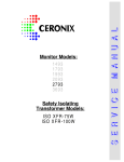
1
Models1492 and 2092
SERVICE MANUAL
2 YEAR LIMITED WARRANTY
This product is warranted by CERONIX to be free of defects in material
and workmanship for a period of two years from the date of purchase.
In case of a fault, developed during this time, it is the customer's
responsibility to transport the defective unit to CERONIX or
one of the authorized service centers for repair.
Please attach a note describing the problem.
All parts and labor are free of charge during the warranty period.
CERONIX
12265 Locksley Lane
Auburn, CA. 95602-2055
(530) 888-1044
This warranty does not cover mechanical breakage due to physical abuse.
CERONIX shall not be liable for any consequential damages, including
without limitation damages resulting from loss of use.
Some states do not allow limitation of incidental or consequential
damages, so the limitation or exclusion may not apply to you.
This warranty gives you specific rights and you may also have
other rights which vary from state to state.
®
®
Recognized under the Component Program
of Underwriters Laboratories Inc. and
the Canadian Standards Association.
COPYRIGHT
© 1988, 1990, 1998
CERONIX
All rights reserved.
The information contained in this manual
is subject to change without prior notice.
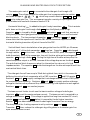
ABOUT THIS MANUAL
This manual is specifically written to aid the service technician, repairing
CERONIX Models 1492 and 2092 color monitors.
There are three main sections:
1. General Description.
2. Circuit Description.
3. Solutions to Problems.
INTRODUCTION
Block
Diagram
Description
BLOCK
Diagram
Schematic
Circuit
Description
Problem
Solving
Tools &
Examples
Appendix
A
Video
Interface
programs
To understand how the Monitor works, it is best to know what each
circuit does and how each circuit relates to the other circuits.
The Block Diagram is presented in a simplified view and a comprehensive
view to accomplish the goal of understanding the whole unit.
Once the general picture is clear, the complexity of each circuit will be easier
to understand.
The Circuit Description is also written in two views, a simplified view
and a detailed view to help give the reader a clear understanding of
what each component does. This understanding is most helpful for the more
complex problems or multiple problems that sometimes occur.
The Trouble Finder section is made up of an index, which lists
symptoms of problems, and a list of possible solutions. Part of this section
also deals with setting up conditions which make it easier to trouble shoot
specific circuits such as the power supply.
1
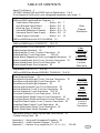
TABLE OF CONTENTS
About This Manual. 1
CERONIX Models 1492 and 2092 Electrical Specification. 3 & 4
Drive Signals to the Monitor Input voltage and waveforms, work sheet. 5
1492 and 2092 Simplified Block Diagram. 6
Video Section Description. - - - - - - - Blocks
Auto Bias and Socket Board. - - - - - - Blocks
Blanking, Sync, & Vertical. - - - - - - - Blocks
Horizontal Deflection & Remote. - - - Blocks
Horizontal Size & Power Supply. - - - Blocks
Power Supply Continued. - - - - - - - - Blocks
A-D
E-G
H-L
M-Q
R-U
V-Y
7
8
9
10
11
12
Block
Diagram
Description
1492 and 2092 Monitor BLOCK DIAGRAM. 13
1492 and 2092 Monitor SCHEMATIC
14 & 15
Video Interface Circuit Description. 16 & 17
Video Interface Schematic. 18
Video Amplifier Circuit, Function, Description. 19
Video Amplifier Circuit Description.
19 & 20
Socket Board, Degaussing Circuit, and Legend Description. 21
Blanking and Master Gain Circuit, Function, Description. 22
Blanking and Master Gain Circuit Description. 23
Blanking and Master Gain Schematic. 24
Video
Socket Board
Blanking
Master Gain
Circuit &
Function
Description
Replacement PARTS LIST. 25 & 28
1492 and 2092 Main Board ASSEMBLY DRAWING. 29 & 30
Block Diagram Review. 31
Auto Bias and Auto Bright Circuit, Function, Description. 32
Auto Bias and Auto Bright Circuit Description. 33
Auto Bias and Auto Bright Schematic. 34
Vertical and Horizontal Sync Circuit Description. 35
Vertical Deflection Circuit, Function, Description. 36
Vertical Deflection Circuit Description. 37 & 38
Horizontal Deflection Circuit Description. 39 & 40
Horizontal Raster Width Control Circuit Description. 41
Horizontal Raster Width and Position Control Schematic. 42
Simplified Power Supply Circuit, Function, Description. 43
Simplified Power Supply Circuit Description. 44
Switch Mode Power Supply Circuit Description. 45
Switch Mode Power Supply Schematic. 46
Auto Bias
Auto Bright
Sync
Vertical
Horizontal
Power Supply
Circuit &
Function
Description
Equipment setup for repairing the Model 1492 Monitor. 47
Problem Solving Tools. 48
Appendix A --- Setup and Convergence Procedure. 49
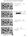
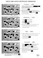
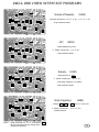
Appendix B --- Video Interface Programs. 50 to 55
Appendix C --- Resistor Array Layout for; B, C, G, H, I, & J.
57 & 58
2
CERONIX
MODELS 1492 and 2092 Electrical Specification
INPUTS
1. Standard Video Configurations, available, are:
A. Positive Analog
Source
Video
.6mA To Amp.
only
Video
Source
Source
D-A 301Ω
301Ω
Gnd
Monitor and
Monitor
{
{
Black level
Saturated color
Black level
Saturated color
1492 & 2092
Min.
Typ.
Max
.05V
0V
0V
3.1V 3.2V 3.3V
.06V
.09V .15V
1.61V 1.69V 1.75V
B. Negative Analog
Video
Source
D-A
To Amp.
Video
905 Ω
Gnd
R IN
V Blk.+.7 V
Monitor
C. 4 Line TTL
R,G,B
Video
Video
Source
*
Intensity
To Amp.
BIAS
Gnd
+12V
VB
Monitor
Red & Green Black level
Blue Black level
Saturated color
Black level
Color on
Low intensity
Full intensity
5.4V
5.6V
4.85V 5.05V
.7V
.9V
0V
2.7V
0V
4.5V
.2V
3.5V
.2V
4.6V
5.8V
5.25V
1.1V
.5V
6.0V
.4V
4.8V
* No pullup resistor on intensity line.
Note: RS170 and other voltage combinations optional for analog video.
2. The Sync signals may be of either polarity and separate or composite.
Hs
1.8K
Sync
High input voltage 2.2V
Source
.15V
Vs
Low input voltage -2.7V
1.8K
Ω,
2
PL
220
Gnd
Horizontal sync pulse 1.5uS
Monitor
Vertical sync pulse 120uS
For composite sync, vertical and horizontal
Horizontal frequency 15.3KHz
sync lines are connected together.
Vertical frequency
45Hz
3. The Power to the monitor is to be
supplied by a secondary winding
of an isolation transformer.
Model 1492
Min.
Typ.
Max.
3.5V
20V
.30V
.80V
4.5uS 31uS
.5mS 1.5mS
15.6KHz 15.9KHz
60Hz
50Hz
65Hz
Model 2092
Min.
Typ.
Max.
115VAC 50Hz or 60Hz 85VAC 115VAC 145VAC 90VAC 115VAC 145VAC
230VAC 50HZ or 60Hz 170VAC 230VAC 290VAC 180VAC 230VAC 290VAC
32W
44W
60W
30W
50W
67W
Power
3
4. The remote Controls are located on
a separate PCB for easy access.
H SIZE--------------Horizontal raster size
V SIZE---------------Vertical raster size
V RAS. POS.-----Vertical raster position
H POS-------Horizontal picture position*
M GAIN---------------------Master gain
Model 1492
Min.
Max.
9.9"
11.4"
6.3"
10.3"
0"
.44"
.9" Right
Dark
Screen
2" Left
Light
Screen
Model 2092
Min.
Max.
14.8"
16.3"
10.0"
14.0"
0"
.60"
1.2 right
Dark
Screen
2.8" left
Light
Screen
The board Controls are located on the main PCB, and are:
Focus on the flyback transformer and an optional Horizontal hold control.
* For start of horizontal sync 1.7uS after end of picture.
5.
Picture
Model 1492
Min. Typ
Max.
.
Rise time 35nS 44nS
49nS
Fall time 32nS 42nS 47nS
Overshoot
0%
0%
2%
Video response is measured at the
tube socket, using low capacitance
coupling. The input signal should
be fully damped and faster than
the expected response.
Band width
Model 2092
Min. Typ
Max.
.
37nS 46nS
52nS
35nS 44nS 50nS
0%
0%
2%
DC
to
8MHz
DC
to
8MHz
Horizontal blank time 12.4uS 12.9uS 13.4uS 12.4uS 12.9uS 13.4uS
20H 1.28mS 20H
20H 1.28mS 20H
Vertical blank time
1%
2%
1%
2%
Horizontal linearity
1%
2%
1%
2%
Vertical linearity
1%
2%
1%
2%
Pincushion
Picture tube
6.
Model 1492
Model 2092
Inch
mm
Inch
mm
Useful diagonal
13
328
20
508
Useful horizontal
10.83
275
16
406.6
Useful vertical
8.13
206.5
12
304.8
86
Useful area
558
192
1,239
Spacing between dot/line trios
.015
.39
.029
.74
Horizontal resolution
680 Pixels
550 Pixels
Vertical resolution
240 Pixels
240 Pixels
Interlaced
480 Pixels
480 Pixels
Deflection angle
90°
90°
Light transmission at center of glass Approximately 46% Approximately 46%
CRT also features: Enhanced contrast, Internal magnetic shield, and
X-Ray output Less than .3mR/hour.
7.
Environmental
Operating temperature
Storage temperature
Operating humidity
Storage humidity
0° C
-20° C
20%
10%
70° C
85° C
80%
95%
0° C
-20° C
20%
10%
70° C
85° C
80%
95%
4
The "Drive Signals To The Monitor Input" form is included here for those people who have
problems interfacing their drive electronics with the Ceronix Monitor.
DRIVE SIGNALS to the MONITOR INPUT
voltage and waveforms, work sheet.
CERONIX
12265 Locksley Lane
Auburn, CA, USA 95602-2055
VIDEO:
Company name:
Date:
Drive signal source
Model number:
For the following measurements use an oscilloscope.
RED GREEN BLUE
With no load the black level voltage is:
With no load the saturated color voltage is:
With 301Ω load
the black level voltage is:
Ω load.
or other
the saturated color voltage is:
To GND, or to
voltage
V.
}
If available, sketch the video drive circuit on the back of a copy of this form.
Horizontal or composite sync:
Horizontal frequency:
Horizontal sync pulse time:
Hz
uS
"High" voltage:
"Low" voltage:
V
V
Hz
uS
"High" voltage:
"Low" voltage:
V
V
Compare your sync to
this table and check
the best fit.
For composite sync.
Sketch if different.
Vertical sync:
Vertical frequency:
Vertical sync pulse time:
Check correct polarity.
Complete form and send to:
CERONIX, 12265 Locksley Lane
If there are any questions, call (530) 888-1044.
Auburn, CA. 95602-2055
5
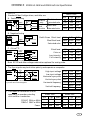
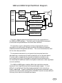
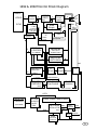
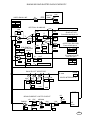
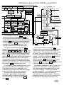
1492 and 2092 Simplified Block Diagram
VIDEO
Output
VIDEO
Interface
GAME
Blanking
SYNC
Output
VIDEO
Amps.
AUTO BIAS
Vertical Deflection
Horizontal Deflection
Remote
Controls
Isolated
Power
CRT
FBT
Horizontal Size
Control
POWER SUPPLY
This block diagram gives a broad view of the circuit organization of
the 1492 and 2092 monitors. The blocks with the bold outline represent
circuits that are quite different than most other monitors.
The auto bias circuit is designed to actively compensate for picture
tube and circuit drift which normally cause the color balance to become
unbalanced and also brightness variation. This circuit eliminates the need
for the color setup procedure.
The horizontal size control circuit permits the horizontal size to be
adjusted from a remote control board instead of a coil on the main board.
It is also used to compensate for pincushion distortion and acts as an
anti-blooming circuit by correcting for horizontal size variations which
are caused by the additional load on the flyback transformer under high beam
current conditions.
The 1492 and 2092 power supplies differ from most other monitors
because of their high efficiency switching mode power supply. It is not
difficult to troubleshoot if the techniques presented in this manual are
clearly understood. Careful reading of all the information presented in this
manual will make trouble shooting of the CERONIX monitor no more difficult
than any other monitor and maybe even easier.
6
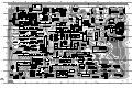
Refer to the block diagram on page 13 (foldout) when reading this description.
A
The Video Interface is designed around a custom IC and will accept positive
or negative analog video signals and also 4 line TTL. This IC also has a
built in multiplier circuit for the master gain control and blanking.
Resistors are used to protect the IC and to set the gain. The programmed gain
is dependent on the input signal amplitude except on TTL. Solder jumpers are
used to program the Video Interface for the type of input signal to be received.
The output of the IC drives the video amplifiers. This drive is a current where
0 mA is black and 4.5 mA is a satur`ted color.
B
The Video Amplifiers are of the push pull type. They are built partly on
thick films and partly on the PCB. Spreading out the amplifier reduces the
component heat and improves the life of the unit. The bandwidth is 8 MHz
with 60Vp-p output. The rise and fall times are .04uS.
C
The Beam Current Feedback circuit directs most of the beam current of each
amplifier to the beam current buffer. The only time this current is measured by
the auto bias circuit is during the time of the three faint lines at the top of the
screen and three lines thereafter. The auto bias circuit is designed to adjust the
video amplifier bias voltage such that the beam current of each of the three guns is
set (programmed), at this time.
D
The Beam Current Buffer converts the, high impedance low current, beam
current signal into a low impedance voltage. This voltage is applied to the
auto bias IC through a 200 ohm resistor. After the three lines of beam
current are measured, the program pulse from the auto bias IC, produces a
voltage drop across this 200 ohm resistor that equals the amplitude of the
beam current voltage.
7
E
The Auto Bias IC is a combination of digital and analog circuitry.
The digital part is a counter and control logic which steps the analog
circuits through a sequence of sample and hold conditions.
The analog part uses a transconductance amplifier to control the voltage on
a 10uF capacitor (one per gun). This voltage is buffered and sent to the
video amplifhers as the bias voltage. In monitors without auto bias, this
voltage has to be set manually using a setup procedure to set the color
balance. With the auto bias, the color balance is set during the end of each
vertical blanking time.
The control sequence is:
1. Grid pulse on G1 causes cathode current (3 lines top of screen)
which is transmitted by the beam current feedback to the
beam current buffer where it is converted to a voltage and
applied to the auto bias input pin.
2.
Auto bias IC outputs a reference voltage at its input pin which
sets the voltage across the coupling capacitor. This coupling
capacitor voltage is directly dependent on beam current.
3.
After the grid pulse is over, the program pulse matches the
voltage from the beam current buffer. If the voltage from the
beam current buffer, during the grid pulse, is the same as the
voltage from the program pulse, the bias is correct and no bias
adjustment is made for that vertical cycle.
F
The aging of the picture tube (CRT) not only affects the balance of the
cathode cutoff voltage, which is corrected by the auto bias circuit, but
it also affects the gain of the CRT. The Auto Bright circuit actively
corrects for CRT gain changes by sensing any common bias change from
the auto bias circuit and adjusts the screen voltage to hold the average
bias voltage constant. The lower adjustment on the flyback
transformer is used to set the auto bright voltage to the center of
its range. This sets up a second control feedback loop to eliminate
picture variation due to the aging of the picture tube.
G
The CRT is a 90° deflection type color picture tube with a 25KV EHT
and has integral implosion protection.
8
H
Blanking is accomplished by setting the gain of the interface IC to zero during
blank time. The Horizontal Blanking pulse is generated by amplifying the flyback
pulse. The Vertical Blanking pulse is started by the vertical oscillator and ended
by the counter in the auto bias IC via the "bias out" pulse. The Master Gain control,
located on the remote PCB, sets the gain of the video signal when blanking is not
active. The Beam Current Limiter circuit, which is designed to keep the FBT from
overloading, will reduce the video gain if the average beam current exceeds .75mA.
I
The Sync Interface can be made to accept separate or composite sync. Two
comparators are used to receive sync, one for vertical sync and the other for
horizontal sync. Resistor dividers are used to protect the comparator IC from
over voltage damage.
J
The Vertical Control circuit consists of:
1.
2.
3.
4.
Vertical sync circuit.
Vertical oscillator.
Linear ramp generator.
Output control and bias circuits for controlling the power driver.
The active components that make up these circuits, except for part of the bias circuit,
are located in the deflection control IC (LA7851). The vertical sync circuit is capable
of accepting either positive or negative going sync pulses without adjustment.
The vertical oscillator in the LA7851 is set at 45 Hz and will sync up to 65 Hz
without adjustment. The deflection yoke is driven with a linear current ramp which
produces evenly spaced horizontal lines on the raster. This linear ramp is generated
by supplying a 1uF capacitor with a constant current. The vertical output voltage is
held within range (biased) by a timer which partly discharges the 1uF ramp capacitor
at the start of vertical retrace. The duration of the timer is controlled by the vertical
output voltage and the vertical auto bias circuit.
K
The Vertical Auto Bias circuit greatly increases the range of the bias circuit built
into the LA7851. It is made up of a negative peak detector and an amplifier which
outputs current to the normal bias circuit, but with a much lower frequency response.
This then eliminates the need for adjustments during production and permits the use
of 50Hz and 60Hz vertical sync with only a size adjustment on the remote control board.
K
The aging of the picture tube (CRT) not only affects the balance of the cathode
cutoff voltage, which is corrected by the auto bias circuit, but it also affects
the gain of the CRT. The Auto Bright circuit actively corrects for CRT gain changes
by sensing any common bias change from the auto bias circuit and adjusts the scre
en voltage to hold the
9
M
The Horizontal Control incorporates a variable sync delay and a phase
locked loop to generate the horizontal timing. The H POS. adjustment on the
remote control board sets the sync delay time which controls the picture position.
The phase locked loop uses the flyback pulse to generate a sawtooth wave
which is gated with the delayed sync pulse to control the horizontal oscillator.
N
The Horizontal Driver supplies the high base current necessary to drive the
horizontal output transistor which has a beta as low as three.
It also protects the horizontal output transistor since it is a transformer and
cannot keep the base turned on for longer than its inductive time constant.
O
The Horizontal Output transistor is mounted to the rear frame which acts as
a heat sink. The collector conducts 1,000 volt flyback pulses which should
not be measured unless the equipment is specifically designed to withstand
this type of stress. A linear ramp current is produced in the horizontal
yoke by the conduction of the horizontal output transistor (trace time).
A fast current reversal (retrace time) is achieved by the high voltage pulse
that follows the turn off of the horizontal output transistor. This pulse is due
to the inductive action of the yoke and flyback transformer.
P
The main function of the Flyback Transformer (FBT) is to generate a
25,000 volt (EHT) potential for the anode of the picture tube. This voltage
times the beam current is the power that lights up the phosphor on the face
of the picture tube. At .75mA beam current the FBT is producing almost 19
watts of high voltage power. The FBT also sources the focus voltage and the
filament power. The FBT has a built in high voltage load resistor which
stabilizes the EHT, for the low beam current condition. This resistor also
discharges the EHT, when the monitor is turned off, which improves the
safety of handling the monitor.
Q
The Remote Control PCB houses the:
CONTROL
1.
2.
3.
4.
5.
DESCRIPTION
CIRCUIT
H SIZE ----------- Horizontal raster size --------- Diode modulator
V SIZE ----------- Vertical raster size ------------- Vertical drive
V RAS. POS. --- Vertical raster position ------- DC current to V. yoke
H POS ------------ Horizontal picture position -- H. sync delay
M GAIN ---------- Master gain ---------------------- Video interface
10
R
The Horizontal Size Control circuit has four inputs:
#
1.
2.
3.
4.
SIGNAL
FUNCTION
Horizontal size ---------------------- Horizontal size control
Beam current ----------------------- Blooming control
Vertical linear ramp ---------------- (#4)-(#3)=Vertical parabolic
Vertical parabolic + V. linear ramp
(Pincushion)
The horizontal size control circuit sums the four signals at one node to
produce the diode modulator control voltage.
S
The Diode Modulator is a series element of the horizontal tuned circuit.
It forms a node between GND and the normal yoke return circuit.
If this node is shorted to GND, maximum horizontal size is present.
A diode is used to control the starting time of the retrace pulse at this node.
The reverse conduction time is dependent on the forward current because the
current waveform at this node has to exceed the forward current in the diode.
A diode, placed in series with the yoke, is then used to control the retrace
pulse amplitude across the yoke. The horizontal size, therefore, is controlled by
controlling the current to this diode via the horizontal size control circuit.
T
A Voltage Doubler is used in the power supply for two reasons:
1. To improve the efficiency of the power supply.
2. To permit 120 volt and 220 volt operation. For the 220 volt
operation the voltage doubler is replaced with a bridge rectifier.
U
The Switching Regulator is synchronized to the horizontal pulse and drives
a power MOSFET. Unlike most regulators that have a common GND, this
power supply has a common V+ and current is supplied from V- to GND.
The MOSFET is connected to V- and signal ground (GND) through a
transformer which is used as an inductor for series switchmode regulation.
An operational amplifier, voltage reference, comparator, and oscillator
in the power supply controller IC are used to accomplished regulation by
means of pulse width modulation.
11
The transformer has two taps on the main winding which are used to
generate the +16 volt and +24 volt supplies. It also has a secondary which is
referenced to V- and supplies the power supply. Since the power supply is
generating its own power, a special start up circuit is built into the power
supply controller IC that delays start up until its supply capacitor is
charged up enough to furnish the current to start the power supply.
This capacitor is charged with current through a high value resistor
from the raw dc supply. This is why the power supply chirps when
an overload or underload occurs.
V
The Load consists of the video amplifiers and the horizontal flyback circuit.
The power supply will not operate without the load since the voltage that
sustains the power supply comes from a secondary in the power transformer
and depends on some primary current to generate secondary current.
W & X
A separate +12V regulator for the video and the deflection circuits are used in this
monitor to minimize raster and video interactions. This also simplifies PCB layout,
since the video GND loops are separate from the deflection GND loops.
Y
The Over Voltage Protect circuit is built into the power supply and monitors the
flyback transformer peak pulse voltage. This circuit will turn off the power
supply and hold it off if the EHT exceeds its rated value. This circuit not only
provides assurance that the X-ray specifications are met but also protects the
monitor from catastrophic failure due to a minor component failure.
12
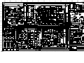
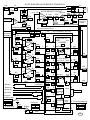
1492 & 2092 Monitor Block Diagram
GAME
VIDEO
VIDEO
3
VIDEO
AMPS.
3
Interface
Bias
A
SYNC
F.B.P.
V retrace
Beam limit
M. gain
H
AUTO BIAS
IC
SYNC
Interface
I
Vs
G
VDY
H DY
3
F
D
Beam current
buffer
Program pulse
Grid pulse
H. blank
V. blank
2
CRT
Feedback
C
Auto
Bright
3
3
Current
B
3
3
BLANKING
Beam
3
E
VERTICAL
CONTROL
VERTICAL
OUTPUT
I. V. Feedback
High Efficiency
L
J
VERTICAL
AUTO BIAS
K
EHT
Hs
HORIZONTAL
CONTROL
Sync delay
H. Pos.
H.
H.
Driver
Output
FBT
O
N
P
M
V. Size &
V. Ras. Pos.
PINCUSHION
2
REMOTE
CONTROLS
(PCB)
DIODE
HORIZONTAL
Size Control
Q
Modulator
R
S
Beam Current
+127V
ISOLATION
Transformer
(IN GAME)
VOLTAGE
DOUBLER
Raw DC
320V
T
V-
LOAD
-200V
(VIDEO & DEFLECTION)
SWITCHING +16V
REGULATOR +27V
Sync U
OVER
VOLTAGE
PROTECT
Y
V
+12V
Video
Regulator Supply
W
+12V Deflection
Zener
Supply
X
13
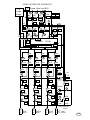
BB
CC
DD
EE
FF
GG
HH
II
JJ
KK
LL
MM
13
0
6
11
3
7
7
8
+12V
392Ω
1.65K
B5
B11
1
B8
82B
7
12
14
8
B2
B19
096
3.3pF
B9
B10
89B
FDH400
83B
WITH GRID
B12
3.32K
B7
GND
VERTICAL BLANKING
129
6.8K
136
138
2
PN2907
1
139
+
155
124
134
3
1N4148
102
1.8K
135
133
8
1/2
LM393
7
1.8K
HORIZONTAL
6.4-7.5VDC BLANKING
8V
63uS
1N4148
4
0Ω
1N4148
1/2
LM393
+
6
1.92.3V
RC7
Master
Gain
RC2
5
1.8K
4
097
.1uF
GND
187
OUT
20
224
+16V
IN
V+
2.7K
2
Hs 56pF
137
132
7.2-8.1VDC
5V 63uS
104
6.8K
1K
.01uF
107
112
197
7
+12V
I2
I1
-9Hz
200K
B
22K
C
TC
4
H7
100K
4.75K
17
RETRACE &
BIAS O/S
DELAYED
SYNC O/S
15
16
V Ref.
14
GND
13
LA7851
RAS. POS.
0 TO 7 VDC
6
7
8
3.6-4.1VDC
1.6V 63uS
3.2VDC
2.9-3.4VDC
0V
5.9VDC
5.7-6.3VDC
.2V 63uS
6.3VDC
5.9-6.4VDC
4V 63uS
11
226
9
25K
330pF
I5
6,10
227
1
10K
230
I13
18
6,800pF
45K
+
228
I6
236
218
9
5.3-6VDC
7.5V 63uS
33K
13
I7
14
I8
1uF
.01uF
233
231
1K
17
2.05K
15
6800pF
I10
232
054
2,200pF
032
6.8K
15.8K
030
033
1.82K
Y
C7
094
+12V
GND
Z
*
62K
016
3.92K
3.92K
013
003
017
R
GIN
14
14
11
5
15
BR
8
340Ω
340Ω
340Ω
038
035
031
L
N
18
13
4K
O
12.1K
023
340Ω
12.1K
024
034
12.1K
340Ω
037
008
340Ω
GND
007
121
120
C2
+
.047uF
14
1/4
LM324
6,800pF
111
.1uF
5
68.1K
C12
118
20
.1uF
4
117
68.1K
C15
C1
1
V. RETRACE
604Ω
604Ω
464Ω
018
044
014
G
8
H
2.7K
052
I
1N4148
1N4148
1N4148
020
042
012
+12V
.1uF
.1uF
025
060
GND
11.5-12.5V
022
041
4.42K
021
043
D 301Ω
E
004
A
9
046
B
005
14
GND
AA
C
027
VC RED VC
4 INPUT 3
GND
P
G
VC GREEN
5 INPUT
270Ω
301Ω
001
75Ω
053
FG
B
VC BLUE
6 INPUT
1.8K
1K
047
048
FRAME
GND
080
8
1
33K
1/2
LM393
4
8
12K
20K
176
C5
2,9
67
HB
5 +
6
116
078
6.8K
1/2
LM393
270Ω
7
+10V
1.8K
VC 4 LINE
0 TTL INPUT
s
VC
1
CC
3
1.22.5V
4
Red
hold
cap.
sw.
normal
Green
hold
cap.
5
1.22.5V
10.6K
18
6
Blue input
5.86.4V
Blue
hold
cap.
303
7
1.22.5V
8
.1.3V
9
10
6.37.7V
PN2222
.5-.8VDC
.7V 17mS
J15
11K
125
16
33K
254A
GND
5V Ref.
PROGRAM
14
246
13
Inrush
Current
Limit
2.2nF
275
275
274
254A
276
279
150uF
250V
100K
1/2W
247
7
8,14
239
3
4
CONTROL &
FAULT SENSE
.1-.5VDC
5
277
5.7-6.3VDC
330pF
288
J6
FR205
248A
248
4uS
DELAY
COMP.
+
.022uF
296
GG
6 Rx
Osc.
7 Cx
285
3.6-4.4VDC
6V 63uS
12
13
5.3-5.7VDC
.10-.17VDC
1V 63uS
OUTPUT
Current
SENSE
DRIVE
38.3K
1,000
pF
J9
291
1.8K
169
271
9
G4
8
2092
22K
166 H. Pincushion
167
Parabolic
62K
50K
163
166A
G9
J11
8.87K
10K
J8
2SK1446LS
D
270
1N4005
283
284
3
13
18Ω
MPSA64
2
HEAT
SINK
10K
G1
GND
267
268
+6V LINE 19 6.8K
6.8K
171
2, 12
GND
G16
.1uF
300
.01uF
1.5KV
306
1N4005
.47uF
250V
8VDC 22V
4V 12Vp-p 17mS
MAX. MIN. H. Size
310
305
2092
.33uF
305
7
750uH
13
18
161
1/4
LM324
G13
316
2SC4159E
0Ω
14 2.2K
278
G14
15 16
HEAT
SINK
16K 17 .01uF
G15
14
185
186
1N4937
311
2.7uF
.022uF
630V
315
8
307
168
CC1
265
150Ω
292
264
CC2
BF5ROM
125
No.
Optional LTR.No.
V-
255
KK
11
2092
8.2nF
306
3,300pF
302
8VDC 23V
70V 250V 63uS
MAX. MIN. H. Size
12 +
164
1
308
200pF
1.2Ω
POWER SUPPLY VOLTAGES REFERENCED FROM VSCOPE GND MUST NOT BE CONNECTED TO GND AND V- AT THE SAME TIME.
3
4
1/4
LM324
6
1N4005
1/2W
298
301
44.2K
*
510Ω
H. Size
2.2K
220uH
167
Linear
13
G11
4
G2
10
38.3K
+12V
J12
2.4-3.6VDC
14V 63uS
1
H.
Width
H. Lin.
68uH
Adj.
.01uF 100K
G10
5
YC4
127VDC
150V 300V
MAX. MIN.
G5
12K
H SIZE
15.8K
14.7K
12
JJ
+6V
18
2,200pF
II
2092
68uH
301
1.00M
1.00M
282
5K
28K Blooming correction.
H. Width
G12
+ 100uF
162
YC3
6VDC
3V 17mS
G17
20
159
.047uF
17
11
J PRA PINS: 3,10,15, & 19
290
20
J10
8 +7.5V REF. V- 9
XRC5184 280
V-
HH
2092
36K
166
1.82K
179
287
V-
0VDC
48V 63uS
NOTES:
5
3.3K
1N4148
191K
16
.1uF
286
238
10K
8
266
244
PC 115VAC PC
2 INPUT 1
FF
FR205
8
1/4
LM324
165
G6
066
433
6VDC
4V
17mS
220K
258
2
1
6-7VDC
+127V
9
6,800pF
90K
18Ω
070
10uF
069 GND
172
10
7
.1uF
7.15K
9
10
184
1/4
LM324
6
6
SMXFR 5
9
4
3
241
Vs
EE
064
HORIZONTAL YOKE
G3
10K
Pincushion correction.
10K 7 5
261
14.8-16.3VDC
INPUT
Output
3.5-4.1VDC
3-4V 63uS
100uF
254
220Vo
131
62K
+
065
10K
178
260
19
J7
FR205
240
245
J3
+15V 16
+17V 15
INPUT Over
Voltage 14
COMP. Protect }
INPUT
3.4-4.2VDC
33.2K
257
3A
FUSE
1.9-2.3VDC
4V
17mS
5
56pF
273
253
150uF
CUT
250V
FOR
256
220Vo
25-.5Ω
C-200
12
PULSE
8.0-9.0VDC
8.4V 17mS
.5-.8VDC
J4
1.8K
252
220Vo
4.6-5.2VDC
EN
21 H. Line Auto
Counter
Bias
CL
Active
Decoder
sw. control
GRID
PULSE
15
.1uF
2
6,800pF 56pF
23.2K
2
FR205
6V Ref.
BIAS
56K
4
J2
2.2nF
143
CL
Start
Counter
FF Q
ERROR
AMP.
6.5-7.5VDC
A
+1.5V
130Ω
2.56.7V
2.7K
154
33K
comp.
VC VERTICAL
2 SYNC
DD
750Ω
4
1K
201
+
1
275
281
17 10uF
sw.
6.5-7.5VDC
.01uF
J16
142
262
183
+ 1,000uF
G7
B
+3V
260Ω
comp.
.1uF
.33uF
GND
INPUT
126
+ 1,000uF
10uF
+
2092
28K
203
203
FR205
+16V
16.3-17.8VDC
J5
2.56.7V
263
251
6
19 10uF
sw.
295
250
33K
141
Green input
250V
294
250V
317
215
249
147
2.56.7V
TZ160B-T3
160V Zener
100K
*
22K
127
20
J14
J1
1 2SA1371E
21 10uF
.1uF
150uF
289
65A
36K
FR205
+27V
20
4.67K
J13
193K
8
+127V
0Ω
297
Beam current limiter circuit.
MPSA64
+6V 270Ω
PN2222
62K
071
D
+12V
GND
+127V
D -3V
2.33K
146
1/4
LM324
comp.
5.86.4V
11
153
GND
5.86.4V
77
061
HORIZONTAL
SYNC H
TH
2
+
.14-.16V
050
75Ω
002
BB
270 Ω
045
PN2907
011
F
301Ω
026
75Ω
R
010
301Ω
301Ω
3
1.8K
.047uF
152
22K
062
051
301Ω
1K
148
10 +
9
Red input
200Ω
C16
5K
2
C -1.5V
sw. in grid pls. pos.
200Ω
C13
5K
19
C14
.047uF
1
17
12
122
C3
1/4
LM324
16
.1uF
7
68.1K
+
2
110
C8
AUTO BIAS IC
1 GND
Vcc 22
CA3224E
123
200Ω
5K
C9
3
C11
6,800pF
7
12
13
4K
144
1/4
LM324
22K
150
.1uF
146
+
6
C10
6,800pF
108
8
4
.1uF
+4.2V
4K
015
GR B IN
15
7
K
312
314
4
1 FIL.
CPT1500
GND
VERTICAL LINEARITY
+10V
145
1.82K
1.8K
M
J
7
103
C4
GND
RR
1
101
Beam
4 Current
5 FIL.
2
V-
063
2.74K
16 13 9 6 11
3
10
5 12
TTL M GAIN
+A EN +12V - A BL
R o G o Bo
BBL
Controls XRC5346A 036
R IN
2
10
C6
Q
X
6
057
2.7K
1.62K
055
.1uF
SCREEN
HL
HR
293
3
FOCUS
7
3
GND
1N4005
1.62K
040
+127V
HORIZONTAL RASTER ADJ. FR205
FR205
E
GND
9
6
8
304
470Ω,1/2W 270Ω, 2W
FBP
1N4005 1N4005
4.2-8.2VDC
5-10 17mS
9
U
056
3
4
309
200Ω 412Ω
909Ω
1
16
F
EHT
2SD1651
GND
+
5
T
237
V-
+200Hz
I16
I15
+800Hz +400Hz
FLYBACK
TRANSFORMER
10
234
157
GND
+127V
2
I11
390Ω, 2W
+27V
H.Fo ADJ. 170Ω
680Ω 340Ω I14
I9 9.31K
2
NO DVM
1KV 63uS
100Ω
20
105
S
TC1
Transformer
2SC4159E
H. V+
10
G
GND
421
182
Hs
GND
423
12.7VDC
33V 63uS Horizontal Drive
235
I12
180
150Ω 1/2W
HORIZONTAL
OSCILLATOR DISCHARGE
5
+ 1uF
418
4,700pF
433
YC2
19
.1-.3VDC
1.4V 63uS
6.8K
1
1K 1/2W
330pF
VERTICAL
DEFLECTION
YOKE
209
19
V
+
comp.
-
4
11
422
2SC3467
16
12
X-RAY
PROTECT
MULTIPLIER
BIAS
SAW TOOTH
TR . GENERATOR
431
EHT
FIL.
.01uF
195
H8
GND
+9Hz
1
1/2W
413
1K 1/2W
1/2W
H11
.36-.4VDC
.6V
63uS
8.2-9VDC
4.4V 63uS
I3
402
7
1K
405
2092
0Ω
405
GND
1,000uF 35V
+
6-6.4VDC
3
1,000
pF
47Ω
424
200K
H3
VERTICAL
OSCILLATOR
D
417
416
415
47Ω 1/2W
5
.68Ω
YC1
H9
223
.7-1.2VDC
.9V 17mS
3.0-3.8VDC
3V 17mS
9
18
4.99K
7.9-8.5VDC
4.4V 63uS
8.8K
1/2W
403
425
15
1N4742
2
22K
470Ω
414
100K 1/2W
200Ω, 2W
11.5-12.5V
12
H6
11
.16-.23VDC
5V 17mS
10
.015uF 250V
10K 1/2W
196
330Ω
76.8K
H18
84K
18
GND
0VDC
47V 63uS
1N4148
H19
CRT
12
1K
13
14,6
500K
Reverse
Hs
12K
1.8K
3
198
1,000pF
205
200
4
410
404
BLUE 11
TC2
.047uF
220
127K
0
8
420
H17
VERTICAL
± SYNC INPUT
1
8
I4
106
PN2222
.068uF
207
15
7
PICTURE
Horizontal
POSITION
O/S
SYNC INPUT
225
0Ω
VIDEO GAIN LINE
5.7-6.6VDC
4V 17mS
19
VERTICAL
100uF
GND 130
.1uF VERT.
206 OSC.
5.8-6.5VDC
4V 17mS
or
Hp5,2
18Ω
RC1
095
1.8K
.047uF
GND
216
128
3.0-3.8VDC
3V 17mS
175
.047uF
7812
.1uF
0Ω
100uF
173
156
.01uF
H14
411
1K 1/2W
2SC3675
1N4005
470uF,50V
190
+ 191
204
Vo
12.4 TO 14V
42V 17mS
9
22K
56pF
208
H4
1.2VDC
25V 17mS
+27V
330pF
118K
7
22-25VDC
1V 16mS
.7-1.0VDC
.9V 17mS
22-25VDC
25V 17mS
210
PCB 490
+12V
GND
H23
H24 GND
068
Remote Control
1K
058
098
H16
17
H10
H22
10uF
10uF
Vs
1K
485
MPS A64
D
3906
34K
6
5
+12V
GND
+12V
93B
1.62K
H13
H5
484
3 7.4-8.4VDC
100
H25 3904
22K
4
193
Bias Control Line
1.21K
200K
301Ω 11
10
202
+10V
6.8K
H15
H20
1N4148
H2
1uF
483
RC4
1.8K
H1
8
Horizontal 20K
Position
1.8K
81B
174
18
22K
88K
330Ω
92B
91B
+12V
1K
3
432
6
408
FDH400
412
TC
3
GRID PULSE
RR
RED
1K 1/2W GREEN
*
2
H12
0Ω 1 330Ω
+12V
3
406
160
RETRACE
BOOSTER
COMP.
INPUT
Retrace
Booster
Vo
18
20
1K
1.8K
2SA1370
B3
B4
181
486
RC3
1.5-2.4V
across
85B
11
1.2K
Vertical
Raster
Position
80-112VDC
Dark screen
90B
27 Ω
2
5.62K
B00
836Ω
88B
4
8.0-9.2VDC
1-2V 4uS
.1uF
0Ω
RC6
1
3.3Ω
510 Ω
2SC3467
5
790Ω
20
180 Ω
B22
3.78K
B16
RC8
750Ω
B13
14
510 Ω
500Ω
482
84B
32 Ω
1000pF
NE592
1.27K
B6
15
19
.015uF
Vertical
Size
.1uF
87B
1
B1
5
SOT
606Ω
2
10
18
0 VDC
2-4V 17mS
GND
0Ω
VERTICAL DRIVE
VERTICAL OUTPUT
VERTICAL 192
POWER
AMPLIFIER
GND
188
481
B15
2SA
68K
1
3
Horizontal
10K
Size
RC5
HEAT
SINK
+12V
+127V
B18
66 Ω
B14
B20
LA7830
270 Ω
20 16 1N4148
1370
86B
17
539Ω
8
1K 1/2W
407
FDH400
1.8-2.3VDC
270Ω
B17
FDH400
11
124-126VDC
40.2K
PCB 428
TC
6
13
Blue Video Amplifier
WITH GRID
Socket Board
20
3
8.9-9.8VDC
1V
4uS
PP
8
13
81G
Green Video Amplifier
8
6
20
81R
Red Video Amplifier
8
NN
TC
10
+
AA
Dual Posistor Optional. 246
LEGEND
BOARD PART No.
PART No. ON PRA.
X
X
PRA PIN No.
DC VOLTAGE
XRANGE, USING
Y V X-Y VDC
A DMM.
X-Y VDC
AC VOLTS CYCLE
Vp-p TIME
Peak to Peak TIME
WAVEFORM
LL
CERONIX
SCALE:
NONE
DRAWN BY:
F. H.
DATE & REV. 1/16/88
1/8/88
5/21/88 2/12/98
9
3/11/88 11/12/90
CERONIX MODEL 1492 MONITOR CIRCUIT
DRAWING
NUMBER
Measured with scope
MM
12265 Locksley Lane
Auburn, California 95602-2055
NN
PP
2ED0114-E
RR
15
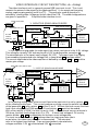
VIDEO INTERFACE CIRCUIT DESCRIPTION (+ & - Analog)
The video interface circuit is a general purpose RGB type input circuit. This circuit
connects the external video signal to the video amplifiers. It can accept positive going
analog, negative going analog, and 4 line TTL. The particular mode of operation is
selected by placing solder bridges on the foil side of the PCB. The solder bridge patterns
are given in appendix A.
Simplified video interface circuit:
Black Level (5.6V)
1. NEGATIVE GOING ANALOG MODE.
+12V
RED channel shown
Saturated Color (1V)
16
7.5V BIAS LINE
VIDEO
AMPS
2.2V
R,G,&B
VIDEO
INPUTS 301Ω
200 Ω
20
604Ω
21
18
3
62K
6.3V
2
C5346
-Analog Black Level
3.6K
MG 12
Connections Installed
36
ALWAYS
(-A BL)
Q&Y
MASTER
GAIN&
BLANKING
NORMALLY
S&X
R
16
In the negative analog mode, the video signal has a black level which is the -A BL voltage.
This voltage is normally 5.6V and may be set to 5.1V by adding solder connection R .
The saturated color is the lowest input voltage (.9V-1.1V). To prevent input line ringing
from exceeding the saturated color voltage limit, a clamp diode 20 has been added.
The current amplitude to the video amplifiers is defined by resistors 21 & 18 and the
master gain voltage.
Saturated Color (1.6V or 3.2V)
2. POSITIVE GOING ANALOG MODE.
+12V
Black Level (.27V)
15.8K 11
16
VIDEO
AMPS
+ANALOG ENABLE
33
R,G,&B
VIDEO
INPUTS
3.6K
200Ω
301Ω
21
D
2
C5346
+12V
36
12.1K
23
A
75Ω
05
RED channel shown
7.5V BIAS LINE
301Ω
04
340Ω
24
MG 12
Connection Installed
ALWAYS NORMALLY
Y
MASTER
GAIN &
BLANKING
D,E,F,G,H,I,
J,K,L,P, & T
3
J
340Ω
38
M
In the positive analog mode, a bias current flows to the input which is set by resistor 33
at the +Analog Enable input. This current produces a voltage, across the parallel resistance
of the (game and 04 ) plus resistor 21 , at the IC pin 2. Without this bias current the black
level input voltage to the C5346 would be 0V and resistor 23 would not be needed.
With a bias resistor of 15.8K, the bias current is .6mA. If the external source resistance is
300 ohms, the black level voltage at pin 2 is .27V. A black level voltage of .3V is set by
resistor divider 23 , 24 to compensate for the bias current voltage drop.
The input termination resistor 04 reduces video line ringing and sets a dark
screen when the video input connector is disconnected. The saturated
color is the highest input voltage. There are two standard, saturated color,
16
voltages available: 1.6V J connected and 3.2V M connected.
VIDEO INTERFACE CIRCUIT DESCRIPTION (TTL)
3. 4 LINE TTL MODE.
+12V
RED channel shown
7.5V BIAS LINE
15.8K
R,G,&B
VIDEO
INPUTS
11
VIDEO
AMPS
+ANALOG EN. &TTL
33
+12V
905 Ω
18 21
200Ω
2.7V
2
C5346
1K (Optional)
04
+12V
INTENSITY
INPUT
16
36
GND
3.92K
03 1.87K
3.92K
13
3.6K
MG 12
Connections Installed
ALWAYS NORMALLY
None
MASTER
GAIN &
BLANKING
A, B, C,
P, & T
5
15
In the 4 line TTL mode the red, green, and blue video lines will pass color when high.
The intensity of the color is set by the fourth TTL line. Saturated color is displayed when
the intensity line is high or open, and when it is low, the displayed color is half intensity.
Although the R, G, and B lines are logic lines, the intensity line is an analog line.
To insure full saturated color, the TTL driver to the intensity line should have no other loads.
The, 1K to GND, input resistor on the color lines may be installed to keep the screen dark when
no video input cable is connected. The logic 0 voltage at the input is 0 to .4V @ .6mA.
The logic 1 voltage at the input is 2.7V to 5.5V @ -2.1mA with the 1K pulldown and .6mA without.
Refer to the video interface schematic to the right for the following component description.
Both the blanking and the gain control is accomplished by the Master Gain line to the video
interface IC (C5346 pin 12). Resistors 054 , 055 , 056 , 057 , & 094
94 provide five
programmable voltages for setting the max. MG voltage. The video gain is also affected by
each of the input modes. Resistors 021 , 018 , 043 , 044 , 011 , and 014 set the video
gain for the -Analog mode and provide protection to the video interface IC inputs in the
+Analog and TTL modes.
Resistors 014 and 030 modify the blue video response in the
Analog mode. The video gain, for the +Analog mode is set by resistors 023 , 024 , 038 ,
034 , 037 , 035 , 008 , 007 , and 031 . The TTL video gain is set by resistors 003 , 013 ,
and 015 . In the +Analog mode, G , H , AND I are bridged to reduce the offset voltage
caused by the bias current. Also, input termination resistors 004 , 026 , and 001 are used
to improve input line matching. In the TTL mode resistors 005 , 027 , and 002 may be 1K &
programmed in. A clamp circuit is used in the -Analog mode to reduce the effect of line ringing.
Resistors 050 and 051 provide a reference voltage which is buffered by PNP transistor 053 ,
load resistor 052 , capacitor 025 , and applied to diodes 020 , 042 , and 012 to perform
this clamping function. P is bridged to reference the clamp to GND for the +Analog and TTL
modes. Resistor 016 is used to set the -Analog black level lower than 5.6 volts.
If the -Analog black level is set below 4.9 volts, both resistors 016 & 017 are used to
override the chip resistor tolerance. The black level for the blue channel may be increased
for all modes by connecting resistor 030 . The C5346 036 has, built in, separate circuits
for each of the three input modes. These modes are selected by bridge points Q & Y .
17
VIDEO INTERFACE SCHEMATIC
P.S. Master Gain line (MG)
To
Video
Amps.
S
T
909 Ω
200 Ω
054
056
040
057
2.7K
Y
094
6.8K
15.8K
62K
030
033
016
+12V
GND
3.92K 3.92K
*
017
013
003
1.87K
Q
X
4.2-8.2VDC
5-10 17mS
1.5K
412 Ω
1.62K
055
.1uF
032
U
R
015
16 13 9 6 11
3
5 12
10
BL
A
TTL
M GAIN
+ A EN +12V
Ro G o B o
BBL
Controls
C5346
036
4
GND
R IN
2
RR
1
GIN
14
GR B IN
15
7
BR
8
340Ω
340Ω
340Ω
038
035
031
J
M
K
N
L
O
12.1K
340 Ω
12.1K
340 Ω
12.1K
340Ω
023
024
034
037
008
007
604Ω
604Ω
464Ω
018
044
014
G
H
I
2.7K
052
1N4148
1N4148
1N4148
020
042
012
+12V
.1uF
.1uF
025
060
GND
4.42K
051
022
041
010
301Ω
301Ω
301Ω
021
043
011
D 301Ω
E
004
A
F
301Ω
026
B
75 Ω
005
C
75 Ω
027
R
G
VC RED
4 INPUT
VC GREEN
5 INPUT
301Ω
053
001
FG
P
1.00K
050
75 Ω
002
B
PN2907
FRAME
GND
GND
HORIZONTAL
SYNC
VC BLUE VC 4 TH LINE
6 INPUT 0 TTL INPUT
18
VIDEO AMPLIFIER CIRCUIT, FUNCTION, DESCRIPTION
The video amplifier, is a high speed push pull amplifier, which can swing as much as 92 volts.
The maximum dynamic output swing is limited to 60 volts. The rest of the output voltage range
is reserved for bias adjustment.
+127V
SIMPLIFIED VIDEO AMPLIFIER CIRCUIT:
270Ω
B14
2SA1370
66Ω
B15
+12V
87B
40.2K
VIDEO
INTERFACE
392Ω
B5
1.65K
B11
606Ω
B6
C5346
790Ω
B9
1
B17
+
NE592
7
68K
B1
.015uF
82B 2SC3467
83B
14
836Ω
B10
27Ω
B3
5.62K
B12
From Auto Bias
control output
+7.9V line
The video amplifier's output voltage, With no input signal, is the black level
which is the picture tube cut off voltage. This voltage is set for each of the three video
amplifiers by the auto bias circuit. This black level voltage has a range of 80V to 112V.
The voltage swing at the output is 60 volts for a 4.3 mA current signal from the C5346.
For this same 4.3 mA current signal the voltage swing at the video amp. input is 1.32 volts and the
-input voltage swing at the NE592 is .75 volts. The reason for using the voltage matching resistor
B6 is that the C5346 minimum output voltage is 7.7 volts, and the bias voltage at the NE592
input is 5.3 volts.
VIDEO AMPLIFIER CIRCUIT DESCRIPTION
The control circuit for the video amplifier is located on the B PRA (B precision resistor array).
The B PRA includes all the Bxx resistors and the NE592. All of the parts labeled xxR
Rxx ,
xxG
xxG , and xxB
xxB , are components located on the circuit board, which are part of the red,
green, and blue video amplifiers.
The video amplifier's stability and precise response to the input signal comes from a
combination of the geometric layout of the B PRA and the high frequency response of the NE592.
The NE592 stabilization capacitor B00 is an integral part of the B PRA conductor layout.
Resistor BB44 is used to boost the NE592 drive current to the PNP transistor 87B
87B .
The NE592 bias circuit, at the input side, consists of BB55 , B6 , and BB99 .
The negative feedback bias resistors are, B11
12 with B
17 as the
B11 , B10 , and BB12
B17
output feedback resistor. Resistors B19 and B20 are connected to solder pads which,
when bridged, permit the 1492 B PRA to be used on the models 1490 and 1491 monitors.
The NE592 gain is set by resistor B8 . The drive signal from the NE592, B22
B22 pin 7,
is coupled to the base of the NPN transistor 83B through an impedance matching resistor B2
B2 .
This drive is also coupled to the base of the PNP transistor 87B
87B via a coupling capacitor 82B
82B .
The NE592 output voltage range is 6V to 10V, which is the reason for the 7.9 volt NPN bias line.
The 7.9 volt bias line is generated by buffering a voltage divider, formed by resistors 097
97
and 100 , with a PNP darlington transistor 098
98 . A capacitor 095
9 5 is connected to
shunt the high current spikes to GND. This line is common to all three video amplifiers.
The AC current gain is set by resistor B3 for the NPN output transistor and by B13
B13
for the PNP output transistor which is AC coupled via a capacitor 84B
.
On
a
positive
84B
output transition of the video amplifier, the current of the PNP transistor can go
as high as 32mA and on a negative transition the current drops to 0mA
19
VIDEO AMPLIFIER SCHEMATIC
6
7
8
Blue Video Amplifier
WITH GRID
+12V
392 Ω
1.65K
B5
B11
40.2K
B17
B14
10
5
B8
12
14
.1uF
B19
3.3pF
B00
790 Ω
836 Ω
B9
B10
.015uF
096
5.62K
B12
GND
+12V
B16
4
8.0-9.2VDC
1-2V 4uS
FDH400
83B
90B
2SA
1370
27 Ω
2
WITH GRID
88B
B3
11
1.2K
3.32K
B4
B7
91B
80-112VDC
Dark screen
1.5-2.4V
across
85B
2.2K
92B
PART OF
AUTO BIAS
2.2K
93B
BIAS CONTROL LINE
3 7.4-8.4VDC
+12V
+12V
VIDEO INTERFACE
MG
G
B13
14
510 Ω
20
84B
32 Ω
19
81B
R
15
180 Ω
510 Ω
B2 2SC
85B
3467
8
5
3.78K
.1uF
87B
1000pF
NE592
B22
18
1
82B
+127V
B15
2SA
7
SOT
1.27K
B1
B18
66 Ω
20 16 1N4148
1370
86B
17
68K
1
3
B6
270 Ω
270 Ω
B20
606Ω
1.8-2.3VDC
124-126VDC
539 Ω
8
13
3
8.9-9.8VDC
1V
4uS
VERTICAL and
HORIZONTAL
BLANKING,
Master Gain, &
Beam limiter
1.21K
100
MPS A64
D
1.62K
097
GND
098
.1uF
095
GND
B
VIDEO SOURCE (external)
For low output distortion, the PNP transistor is biased with a 6 mA current. The NPN
transistor and resistor B
17 conduct the PNP bias current to GND. Diode 86B balances the
B17
PNP base to emitter voltage. Resistors B1 and B14
B14 set the voltage across B15
B 15 which
define the video amplifier output stage bias current. A quick way to check this current, is to
measure the voltage drop across the 510 ohm 85B . The permissible voltage range is
listed on the schematic as 1.5-2.4V. The PNP and NPN collector resistors B16 and 85B
help stabilize the amplifier and provide some arc protection. Resistor BB18
18 is used to decouple
the video amplifiers from the +127V line. Capacitor 096
96 is used to decouple the +12 volt line
close to the video amplifiers. If this capacitor or the 7.9V line capacitor 095 is open, the
video may be unstable and distorted. Resistor B7
B7 is the auto bias output load resistor.
If there is a problem with the video, first check the output waveform of the video amplifier,
with the oscilloscope, if ok the problem is not in the video section. If not ok, check the input
waveform at B PRA pin 8, if not ok there, check the video interface, If ok at the video amplifier
input, refer to this section to help with analyzing the video amplifier problems.
20
SOCKET BOARD , DEGAUSSING CIRCUIT, AND LEGEND DESCRIPTION
TC
10
8
PCB 428
TC
6
FDH400
1K 1/2W
407
406
FDH400
TC
3 GRID PULSE
RED
1K 1/2W GREEN
8
411
FDH400
1K 1/2W
410
404
BLUE 11
12
*
.1uF 250V
470Ω
412
414
1/2W
403
10K 1/2W
2SC3675
100K
417
416
200K
420
100K 1/2W
47Ω
424
10
6
408
425
TC
4
432
Socket Board
415
9
5
.68Ω
405
2092
0Ω
405
47Ω
402
GND
7
1
431
1K
1K 1/2W
422
EHT
1/2W
413
1K 1/2W
EHT
FOCUS
SCREEN
418
330pF
2,200pF
423
421
FIL.
FBT
TC1
TC2
FIL.
FIL.
The primary function of the socket board is to connect the main board to the CRT and to
CC1
protect the main board against arc related voltage spikes which originate in the CRT.
The tube socket has built in spark gaps which direct part of the arc energy to the
403 . The remaining high voltage
tube ground (aquadag) through a dissipation resistor 403
CC2
406 , 406
411 , and 411
404 and
from an arc is dropped across current limit resistors: Resistors 404
407 , 408
408 , & 410
410 protect the video amplifiers by directing the arc energy to
diodes 407
BF
capacitor 414
414 . Since arcing does not normally occur in rapid succession, capacitor 414
414
5ROM
is left to discharge by the leakage current of diodes 407 , 408
408 , & 410
410 and zener
125
diode 412
412 is not normally used. The grid pulse transistor is protected by a low pass filter
244
made up of resistors 422
422 & 425
425 and capacitor 423
423 . The auto bright transistor 417
417
is protected by resistors 416
416 & 420
420 and by a low pass filter comprised of
resistors 413
413 , 418
418 , & 415
415 and capacitor 421
421 . Resistors 402
402 & 424
424
3A FUSE
reduce the arc energy from the tube ground to signal GND.
245
The current gain of the auto bright control loop is set by resistor 420
420 .
The filament current is fine tuned by resistor 405
405 .
The degaussing coil 432
432 is energized when power is turned on.
It then rapidly turns off due to the heating of posistor 244
244 .
241
PC
115VAC PC
Legend Description
2 INPUT 1 238
the 1492 board part number. The parts list gives the
No.
{ Represents
CERONIX PART NUMBER which is indexed to the board part number.
LTR.No.
Part numbers of the resistors on the PRA indicated by LTR.
LEGEND
PRA
pin
number.
To
determine
which
PRA
the
pin
number
X
X
{ belongs to, look for the nearest PRA part number on that line. No.
BOARD PART No.
XYV
X-Y VDC
DC voltages are measured to GND except in the power supply
where V- is the reference. Use a DVM for DC measurements.
X-Y VDC
Vp-p TIME
WAVEFORM
TIME is the cycle time of the waveform.
waveform is normally checked with a oscilloscope.
{ The
It has a P-P voltage amplitude of Vp-p .
LTR.No.
X
X
PART No. ON PRA.
PRA PIN No.
DC VOLTAGE
XRANGE, USING
Y V X-Y VDC
A DMM.
X-Y VDC
AC VOLTS CYCLE
Vp-p TIME
Peak to Peak TIME
WAVEFORM
CAUTION: When making measurements on the power
supply be sure that the other scope probe is not connected to GND.
Measured with scope
21
BLANKING AND MASTER GAIN CIRCUIT, FUNCTION, DESCRIPTION
Blanking in this monitor is accomplished by reducing the video gain to zero during the
vertical and horizontal blank time. During video time, the gain is set by the master
gain control which is located on the remote control PCB. If the overall beam current
exceeds .75mA for more then ten frames, the beam current limiter circuit will reduce the
video gain to protect the FBT.
SIMPLIFIED GAIN CONTROL CIRCUIT:
GAIN SELECT
RESISTORS
+12V
1K
MASTER GAIN
1K
VIDEO INTERFACE
VIDEO GAIN LINE
C5346
Video
Amp.
36
58
485
3.6K
HORIZONTAL BLANKING
FLYBACK PULSE
0VDC
47V 63uS
To
CRT
200Ω +7.5V
PN2222
One of three input circuits.
SIGNAL
CONDITIONING
CIRCUIT
BIAS ACTIVE
LM393
6 +
155
BEAM CURRENT LIMITER
+6V
2
5
Vertical Bias O/S 1/2
104
VERTICAL BLANKING
+2V
HIGH Z
+2V
+
+12V
7
1N4148
134
.047uF
MPSA64
1/2
LM393
1
PN2222
D
3 +
65
63
Total
beam current
From FBT
10uF
66
132
The video P-P voltage amplitude at the cathodes, is the video input signal amplitude times
the master gain control setting times the video amplifier gain. The gain select resistors set
the maximum video gain via the master gain line. For a greater range of brightness,
(highlighting) the video system is allowed to supply high peak video currents which could
damage the FBT if sustained. The beam current limiter circuit insures that the long term
maximum beam current is not exceeded.
104 .
Horizontal blanking is achieved by amplifying the flyback pulse (FBP) with transistor 104
Vertical blanking starts as soon as the LA7851 starts the vertical retrace sequence and is
terminated by the auto bias, bias active signal. A comparator is used to sense the vertical bias
132
O/S, at pin 16 of the LA7851, which goes low when vertical retrace starts. Capacitor 132
holds the vertical blanking active, between the vertical bias O/S pulse, and the bias active pulse.
132 is reset and vertical blanking ends,
When the bias active line goes high, the capacitor 132
after the bias active line returns to it's high impedance state.
22
BLANKING AND MASTER GAIN CIRCUIT DESCRIPTION
The master gain control 485 is connected to the video gain line through a 1K
58 . The voltage range of the video gain line is programmable via resistor 094
resistor 58
094
54 , 55
55 , 56
56 , and
and solder bridges at S , TT , & U
U which may connect resistors 54
57
57 to the video gain line. This arrangement permits a variety of input signals and
picture tubes to be used with the same monitor PCB.
Horizontal blanking ( H B ) is added to the gain line by transistors 104 . This transistor
102 when the flyback pulse is high.
pulls down on the gain line through diode 102
105 , 106 and resistor 112
Capacitor 197 is charged by diodes 105
112 such that, as soon as
the flyback pulse starts going positive the NPN transistor 104 turns on and horizontal
blanking starts. The time constant of capacitor 197 and resistors 112
112 and 107 is
chosen such that the capacitor will lead the FBP on the downward slope and turn the
horizontal blanking transistor off just at the end of the FBP.
Vertical blank time is started when a low going pulse from the LA7851 pin 16 causes
the output, pin 7, of the dual comparator 155 to go low. Capacitor 132 is discharged
through resistor 135
135 at this time. After the end of the LA7851 pulse, the capacitor 132
holds the output, pin 1 of the comparator, low until the bias active pulse recharges the
134 . During the high time of the bias active pulse, the
capacitor 132 through diode 134
134 .
second comparator output is still low, because of the voltage drop across the diode 134
The end of vertical blank time occurs when the bias active line returns to it's high
impedance state. The capacitor 132 holds the charge from the bias active pulse until the
next vertical blank time.
The video gain line will source up to 32mA during blank time, which is the reason for
buffering the vertical blank comparator with a PNP transistor 139
139 and E-B resistor 129 .
138 supply a voltage that is midrange relative to the LA7851 pulse
Resistors 137 and 138
for maximum noise immunity. Resistors 133 and 136 also supply another midrange
voltage for the bias active pulse and the, vertical blanking, hold capacitor to work against.
Resistors 124 and 156 are used as jumpers.
The beam current limiter circuit uses the base to emitter voltage of a darlington
transistor 65 to set the maximum beam current. The beam current is converted to a
voltage across resistor G17 . This voltage is applied to a long time constant RC circuit,
70
66 , before it is sensed by the darlington transistor.
resistor 70
and capacitor 66
65A
Resistor 65
A has been added to protect the darlington transistor from arc energy.
64 and 71
71 .
The sharpness of the limiting response is set by resistors 64
63 then, reduces the video gain by pulling down on the master gain line
Transistor 63
upon excessive beam current.
23
BLANKING AND MASTER GAIN SCHEMATIC
Remote control PCB
1K
VIDEO GAIN LINE
MASTER
GAIN
RC2
1K
485
GND
058
4.2-8.2VDC
5-10 17mS
+12V
VERTICAL BLANKING
FROM AUTO BIAS SUPPLY
+10V
1.8K
136
2
MPS2907
1
1/2
LM393
139
+
155
3
63uS
5
4
1.9-2.3VDC
4V
17mS
1.92.3V
1.8K
(VERTICAL BIAS O/S)
From LA7851 pin 16
156
3.0-3.8VDC
3V 17mS
1.8K
.047uF
1N4148
137
132
GND
106
6.8K
1K
.01uF
(FLYBACK PULSE)
From FBT pin 8
107
1N4148
105
112
197
0VDC
47V 63uS
PN2222
104
+
135
133
6
1/2
LM393
1.8K
1.8K
HORIZONTAL
6.4-7.5VDC BLANKING
8
124
7
134
(BIAS ACTIVE)
From auto bias IC pin 13
138
0Ω
1N4148
1N4148
102
8V
6.8K
6.8K
129
HB
TO AUTO BIAS IC
GND
GAIN SELECT RESISTORS
S
T
U
909Ω
200Ω
412 Ω
054
056
057
M
1.62K
10K
040
094
GAIN
C5346
036
VIDEO INTERFACE IC
1.62K
055
+12V
GND
FBT
+6V
BEAM CURRENT LIMITER CIRCUIT.
+6V
PN2222
063
270Ω
071
1.8K
MPSA64
D
750Ω
065
064
GND
62K
62K
065A
070
GI7
EHT
Return
+ 10uF
066
24
BB9
BB9
CC6
AA9
AA9
A2
A2
A2
B1
B2
B1
B1
B1
CPR0132 B2
BB8
BB8
BB8
BB6
BB7
BB6
BB6
BB6
AA7
Optional input filter capacitor.
301 ohm ±1%, .25W
1N4148 10mA, 75V Diode
3.92K ohm ±1%, .25W
464 ohm ±1%, .25W
1.8K ohm ±5%, .25W
62K ohm ±5%, .25W
Optional -BL adjust resistor.
604 ohm ±1%, .25W
CPD1251 B1 AA8
CPR0128 B2 AA8
B2 AA8
CPR0144 B2 AA7
CPR0129 C2 AA7
CPC1039 C2 CC8
CPR0128 C2 BB9
CPR0124 C2 BB9
CPR0050 A2
1N4148 10mA, 75V Diode
301 ohm ±1%, .25W
Optional input filter capacitor.
12.1K ohm ±1%, .25W
340 ohm ±1%, .25W
.1uF ±5% @ 50V
301 ohm ±1%, .25W
75 ohm ±1%, .25W
0 ohm Jumper
CPR0013
CPR0129
CPC1039
CPR0145
CPR0144
CPR0129
CPI1409
CPR0129
CPR0129
CPR0128
CPD1251
CPR0140
CPR0131
CPR0011
CPR0018
301 ohm ±1%, .25W
75 ohm ±1%, .25W
3.92K ohm ±1%, .25W
301 ohm ±1%, .25W
75 ohm ±1%, .25W
6 Conductor Header.
BB7 340 ohm ±1%, .25W
BB7 12.1K ohm ±1%, .25W
A2
A2
A2
A2
B3
B2
B2
B2
B2
AA6
BB7
AA5
AA6
AA7
BB7
AA6
BB7
AA7
6.8K ohm ±5%, .25W
340 ohm ±1%, .25W
.1uF ±5% @ 50V
15.8K ohm ±1%, .25W
12.1K ohm ±1%, .25W
340 ohm ±1%, .25W
XRC5346A Custom Video IC
340 ohm ±1%, .25W
340 ohm ± 1%, .25W
CPR0136 B2
C2
CPD1251 C2
CPR0128 C2
CPR0132 C2
CPR0004 D1
CPR0011 D1
CPR0011 D1
CPR0004 D1
BB5
BB8
AA8
AA8
AA7
DD8
CC8
CC9
DD8
1.62K ohm ±1%, .25W
Optional input filter capacitor.
1N4148 10mA, 75V Diode
301 ohm ± 1%, .25W
604 ohm ±1%, .25W
270 ohm ±5%, .25W
1.8K ohm ±5%, .25W
1.8K ohm ±5%, .25W
270 ohm ±5%, .25W
CPR0009 D1 CC9 1K ohm ±5%, .25W
.01
.01
.01
.01
.01
.22
.01
.01
.01
.01
.01
.01
.01
.01
.01
.01
.01
.01
.01
.05
.01
.01
.01
.01
.01
.05
.01
.01
.01
1.51
.01
.01
.01
.01
.01
.01
.01
.01
.01
.01
.01
051
052
053
054
055
056
057
058
059
060
061
062
063
064
065
065A
066
067
068
069
070
071
072
073
074
075
076
077
078
079
080
81B
82B
83B
84B
85B
86B
87B
88B
89B
90B
91B
92B
93B
094
095
096
097
098
099
100
CERONIX
PART No.
CPR0141
CPR0012
CPQ1301
CPR0126
CPR0136
CPR0127
CPR0130
CPR0009
D1
C1
C2
D2
D2
D2
D2
C2
CC8
CC8
CC8
AA5
AA5
AA5
BB5
EE3
4.42K ohm ±1%, .25W
2.7K ohm ±5%, .25W
PN2907 .6A, 40V, .6W, PNP
909 ohm ±1%, .25W
1.62K ohm ±1%, .25W
205 ohm ±1%, .25W
412 ohm ±1%, .25W
1K ohm ±5%, .25W
.01
.01
.06
.01
.01
.01
.01
.01
D1
D1
D1
D1
D2
D2
D2
D2
E1
E2
D1
E2
E2
E1
E1
E1
E1
E1
CPR0011 E1
CPR0009 E2
CC8
DD9
DD8
PP5
PP5
PP5
RR5
RR5
DD8
GG2
PP5
RR5
PP5
.1uF ±5% @ 50V
270 ohm ±5%, .25W
22K ohm ±5%, .25W
PN2222A .6A, 30V, .5W, NPN
750 ohm ±5%, .25W
MPSA64 .3A, 30V, D-PNP
62K ohm ±5%, .25W
10uF ±20% @ 50V
LM393 Dual Comparator
10uF ±20% @ 50V
.1uF ±5%, @ 50V
62K ohm ±5%, .25W
270 ohm ±5%, .25W
.05
.01
.01
.05
.01
.08
.01
.04
.31
.04
.05
.01
.01
E1
C3
A3
A3
C3
B3
C3
C3
C3
C3
C3
C3
C3
C4
B3
A3
B3
A4
A4
DD8
CC1
CC1
CC2
DD1
CPC1039
CPR0004
CPR0015
CPQ1303
CPR0007
CPQ1302
CPR0018
CPC1101
CPI1410
CPC1101
CPC1039
CPR0018
CPR0004
CPR0013
CPR0500
CPC1040
CPQ1308
CPC1037
CPR0050
CPD1251
CPQ1309
CPC1005
CPR0006
CPD1250
CPQ1309
CPR0011
CPR0011
CPR0012
CPC1039
CPC1039
CPR0136
CPQ1302
PRICE
A1
A1
B1
B1
B1
C1
A2
A2
BOARD No.
CPR0128
CPR0124
CPR0140
CPR0128
CPR0124
CPS1754
CPR0129
CPR0144
DESCRIPTION
PRICE
CERONIX
PART No.
Models 1492 and 2092
Board Ref.
Schematic
Reference
001
002
003
004
005
006
007
008
009
010
011
012
013
014
015
016
017
018
019
020
021
022
023
024
025
026
027
028
029
030
031
032
033
034
035
036
037
038
039
040
041
042
043
044
045
046
047
048
049
050
REPLACEMENT PARTS LIST
Board Ref.
Schematic
Reference
BOARD No.
Board No.s 001 to 100
DESCRIPTION
EE9 1.8K ohm ±5%, .25W
EE8 1K ohm ±5%, .25W
CC1
CC1
DD2
CC2
DD2
DD2
DD2
DD2
BB5
DD3
BB2
CC3
DD3
.01
.01
6.8K ohm ±5%, .25W
Blue Video Amplifier
.015uF ±10% @ 250V
2SC3467AE .1A, 200V, 1W, NPN.
.1uF ±10% @ 250V
0Ω Jumper
1N4148 10mA, 75V Diode
2SA1370E .1A, 200V, 1W, PNP
1000pF ±20% @ 500V
510 ohm ±5%, .25W
FDH400 .1A, 200V, Diode
2SA1370E .1A, 200V, 1W, PNP
1.8K ohm ±5%, .25W CF
1.8K ohm ±5%, .25W CF
2.7K ohm ±5%, .25W
.1uF ±5% @ 50V
.1uF ±5% @ 50V
1.62K ohm ±1%, .25W
MPSA64 .3A, 30V, D-PNP
CPR0134 B4 CC3 1.21K ohm ±1%, .25W
.01
1.12
.07
.16
.07
.01
.01
.19
.03
.01
.03
.19
.01
.01
.01
.05
.05
.01
.08
.01
25
101
102
103
104
105
106
107
108
109
110
111
112
113
114
115
116
117
118
119
120
121
122
123
124
125
126
127
128
129
130
131
132
133
134
135
136
137
138
139
140
141
142
143
144
145
146
147
148
149
150
151
152
DD5
AA4
DD5
AA4
BB4
BB4
BB4
DD6
1N4005 1A, 600V, R-Diode
1N4148 10mA, 75V, Diode
1N4005 1A, 600V, R-Diode
PN2222A .8A, 40V, .5W, NPN
1N4148 10mA, 75V, Diode
1N4148 10mA, 75V, Diode
6.8K ohm ±5%, .25W
6800pF ±10% @ 100V
CPC1028 C5 DD7 6800pF ±10% @ 100V
CPC1028 C5 DD7 6800pF ±10% @ 100V
CPR0009 D5 BB4 1K ohm ±5%, .25W
CPS1756
CPR0506
CPC1036
CPC1039
CPC1036
"TC" 10 Conductor Header
D4
"C" PRA (Auto Bias)
C5
A5 EE7 .047 uF ±5% @ 50V
B5 EE7 .1 uF ±5% @ 50V
B5 EE7 .047uF ±5% @ 50V
CPC1039
CPC1036
CPC1039
CPI1402
CPR0050
CPC1101
CPC1101
CPC1101
CPC1039
CPR0011
CPI1407
CPC1104
CPC1036
CPR0011
CPD1251
CPR0011
CPR0013
CPR0011
CPR0013
CPQ1301
CPR0050
CPR0016
CPR0016
CPR0016
CPC1039
CPD1252
CPI1405
CPR0015
CPR0015
B5
B5
B5
A6
A6
B6
B6
B6
A7
A6
A7
B7
B7
C7
C7
C7
C7
C7
C6
A6
C6
C6
C6
C6
B6
C5
C5
C6
C6
EE6
EE6
EE6
FF7
CC3
FF7
FF6
FF6
EE3
AA3
EE3
JJ6
BB4
BB4
BB3
BB4
BB3
CC4
CC3
AA3
GG6
GG7
GG7
EE5
DD5
GG6
GG6
GG6
.02
.01
.02
.05
.01
.01
.01
.03
.03
.03
.01
.29
.68
.04
.05
.04
.1uF ±5% @ 50V
.05
.047uF ±5% @ 50V
.04
.1uF ±5% @ 50V
.05
1.95
CA3224E Auto Bias IC
0 ohm Jumper.
.01
10uF ±20% @ 50V
.04
10uF ±20% @ 50V
.04
10uF ±20% @ 50V
.04
.1uF ±5% @ 50V
.05
1.8K ohm ±5%, .25W
.01
NJM7812FA 12V, 1A, Regulator.
.30
1000uF ±20% @ 35V
.22
.047uF ±5% @ 50V
.04
1.8K ohm ±5%, .25W
.01
1N4148 10mA, 75V, Diode
.01
1.8K ohm ±5%, .25W
.01
6.8K ohm ±5%, .25W
.01
1.8K ohm ±5%, .25W
.01
6.8K ohm ±5%, .25W
.01
MPS2907 .6A, 40V, .6W, PNP .06
0 ohm Jumper
.01
33K ohm ±5%, .25W
.01
33K ohm ±5%, .25W
.01
33K ohm ±5%, .25W
.01
.1uF ±5% @ 50V
.05
1N4005 1A, 600V, R-Diode
.02
LM324 Quad Op. Amp.
.31
22K ohm ±5%, .25W
.01
22K ohm ±5%, .25W
.01
CPC1039 C6 GG5 .1uF ±5% @ 50V
CPR0050 D6
0 ohm Jumper
CPR0016 C6 EE8 33K ohm ±5%, .25W
.05
.01
.01
153
154
155
156
157
158
159
160
161
162
163
164
165
166
166
166A
167
167
168
169
170
171
172
173
174
175
176
177
178
179
180
181
182
183
183A
184
185
186
187
188
188A
189
190
191
192
193
194
195
196
197
198
200
CPQ1303
CPR0012
CPI1410
CPR0011
CPR0393
CPS1755
CPR0011
CPR0050
CPC1039
CPC1036
CPC1032
CPR0018
CPI1405
CPR0144
CPR0017
CPR0018
CPR0168
CPR0015
CPC1032
CPC1102
CPR0504
CPR0013
CPR0142
CPR0050
CPR0050
CPR0050
CPR0144
CPR0050
CPR0009
CPR0024
CPQ1308
CPR0050
CPR0351
CPC1041
CPR0050
CPR0143
CPQ1307
CPM2037
CPC1036
CPM2036
CPM2037
CPD1252
CPC1109
CPI1401
CPR0377
CPR0050
CPC1104
CPR0391
CPC1032
CPC1000
CPR0157
C6
C6
C7
D7
D7
C2
F3
D2
E2
E2
E2
E2
E2
E3
E3
E3
E3
E3
E3
E2
F3
F3
E3
D3
D3
D3
D3
E3
E3
F3
E4
E3
E3
E4
E3
E3
F3
G3
D4
E4
F4
E4
E4
E4
F4
F4
G4
D5
D5
D5
E5
EE9
DD9
BB3
CC4
MM4
MM7
LL0
NN8
MM7
NN7
NN8
NN7
NN7
NN7
NN7
NN7
NN7
PP8
MM7
MM8
NN5
GG4
GG1
GG2
EE8
NN5
MM7
MM2
GG1
NN3
MM5
NN6
PP8
PP8
GG3
GG1
GG1
KK1
KK1
HH1
GG2
MM2
JJ2
BB4
EE4
HH2
Models 1492 and 2092
PRICE
CERONIX
PART No.
Board Ref.
Schematic
Reference
A5
A5
B5
B5
B5
B5
B4
C5
DESCRIPTION
BOARD No.
CPD1252
CPD1251
CPD1252
CPQ1303
CPD1251
CPD1251
CPR0013
CPC1028
REPLACEMENT PARTS LIST
PRICE
CERONIX
PART No.
Board Ref.
Schematic
Reference
BOARD No.
Board No.s 101 to 200
DESCRIPTION
PN2222A .6A, 30V, .5W, NPN
2.7K ohm ±5%, .25W
LM393 Dual Comparators
1.8K ohm ±5%, .25W
390 ohm ±5%, 2W
"RC" 8 Conductor Header
1.8K ohm ±5% (Blooming adjust)
0 ohm Jumper
.1uF ±5% @ 50V
.047uF ±5% @ 50V
.01uF ±5% @ 50V
62K ±5%, .25W (2092 Option)
LM324 Quad Op. Amp.
12.1KΩ ±1%.25W (Pin. Adj) 1492
36KΩ ±5%, .25W (Pin. Adj) 2092
62KΩ ±5%, .25W (H. Ras. Adj.)
8.06KΩ ±1%.25W (Pin. Adj) 1492
22KΩ ±5%, .25W (Pin. Adj) 2092
.01uF ±5% @ 50V
100uF ±20% @ 25V
"G" PRA (H. Width Control)
6.8K ohm ±5%, .25W
7.15K ohm ±1%, .25W
0 ohm Jumper
0 ohm Jumper
0 ohm Jumper
12.1K ohm ±1%, .25W
0 ohm Jumper
1K ohm ±5%, .25W
3.3KΩ ±5% .25W (Max. iBeam adj.)
2SC3467F .1A, 200V, 1W, NPN
0 ohm Jumper
150 ohm ±10%, .5W, CC
.33uF ±5% @ 50V
0 ohm Jumper
10.0K ohm ±1%, .25W
2SC4159E 1.5A, 180V, 15W, NPN
Heat Sink, H. Width output
.047uF ±5% @ 50V
Heat Sink, V. Deflection out
Heat Sink (2092 Option)
1N4005 1A, 600V, R-Diode
470uF ±20% @ 50V
LA7830 Vert. Def. Output
3.3 ohm ±5%, 1W
0 ohm Jumper
1000uF ±20% @ 35V
200 ohm ±5%, 2W
.01uF ±5% @ 50V
56pF ±5% @ 100V
127K ohm ±1%, .25W
26
.05
.01
.31
.01
.04
.26
.01
.01
.05
.04
.04
.01
.31
.01
.01
.01
.01
.01
.04
.05
.92
.01
.01
.01
.01
.01
.01
.01
.01
.01
.16
.01
.05
.08
.01
.01
.36
.11
.04
.13
.11
.01
.02
.19
.67
.03
.01
.22
.04
.04
.03
.01
201
202
203
203
204
205
206
207
208
209
210
211
212
213
214
215
216
217
218
219
220
222
223
224
225
226
227
228
229
230
231
232
233
234
235
236
237
238
239
240
241
242
243
244
245
246
247
248
248A
249
250
251
MM5
GG2
MM5
MM5
JJ1
JJ2
HH2
HH2
II1
NN2
JJ2
.04
.17
.01
.01
.03
.03
.05
.04
.03
.04
.04
CPS1759
CPR0503
CPC1104
CPC1102
E5
E5
E5
E5
F5
F5
F5
F5
F5
F5
F5
F5
F5
G5
F5
D6
D6
10uF ±20% @ 50V
1.0uF ±5% @ 50V
36K ohm ±5%, .25W 1492
28.0KΩ ±1%, .25W
2092
56pF ±5% @ 100V
1000pF ±20% @ 500V
.1uF ±5% @ 50V
.01uF ±5% @ 50V
330pF ±10% @ 100V
.01uF ±5% @ 50V
.047uF ±5% @ 50V
Vertical Deflection Bias Adj.
Vertical Deflection Bias Adj.
4X .062 Dia. Bead Pins (YC)
HH2 "H" PRA Vertical Control
JJ6 1000uF ±20% @ 35V
GG3 100uF ±20% @ 25V
.01
1.26
.22
.05
CPI1400
E6 KK3 LA7851 V. & H. Control IC
1.48
CPC1036
CPR0502
CPD1257
CPR0002
CPC1102
CPC1026
CPC1025
CPC1028
F5
F6
D6
D6
D6
E6
E6
E6
II1
KK4
JJ2
GG3
GG3
HH4
HH4
II4
CPC1100
CPC1032
CPC1027
CPC1100
CPC1003
CPR0138
CPQ1307
CPT1505
CPS1753
E6
F6
F6
F6
F6
F7
F7
E7
F1
F1
F1
F2
F2
F2
F3
F3
G1
G2
G2
G2
G2
G3
H3
II4 1uF ±20% @ 50V
JJ4 .01uF ±5% @ 50V
JJ4 6800pF ±5% @ 100V
JJ4 1uF ±20% @ 50V
MM3 2,200pF ±20% @ 1KV
KK4 2.05K ohm ±1%, Hfo adjust.
MM3 2SC4159E 1.5A, 180V, 15W, NPN
NN3 Horizontal Drive Transformer
GG9 "PC" 2 Conductor Header
GG9 Optional AC noise capacitor.
GG9 C-200-7, 25-.5Ω Inrush Current Limiter
GG9 Optional AC line capacitor.
"CC" .093 Dia. Bead Pins
"CC" .093 Dia. Bead Pins
LL9 BF5ROM125 Posistor (Optional)
GG9 SS1-3A 3 AMP FUSE
LL9 Dual Posistor (Optional)
HH8 100K ohm ±5%, .5W, CF
KK6 FR205 2A, 600V, F-Diode
JJ6 18 ohm ± 5%, .25W
HH6 Optional 127V line control.
HH6 2SA1371E .1A, 300V, 1W, PNP
HH6 100K ohm ±5%, .25W
CPC1101
CPC1043
CPR0017
CPR0163
CPC1000
CPC1005
CPC1058
CPC1032
CPC1002
CPC1032
CPC1036
CPR0426
CPS1758
CPS1758
CPRO427
CPR0425
CPRO430
CPR0366
CPD1264
CPR0002
CPQ1310
CPR0019
.047uF ±5% @ 50V
"I" PRA Horizontal Control
1N4742 12V ±5%, 1W, Z. DIODE
18 ohm ±5%, .25W
100uF ±20% @ 25V
1000pF ±5% @ 100V
330pF ±5% @ 100V
6800pF ±10% @ 100V
.04
.68
.05
.01
.05
.06
.06
.03
.04
.04
.06
.04
.03
.01
.36
.60
.21
.28
.02
.02
.96
.25
.01
.04
.01
.22
.01
252
252A
253
254
254A
254B
255
256
257
258
259
260
261
262
263
264
265
266
267
268
269
270
271
272
273
274
275
276
277
278
279
280
281
282
283
284
285
286
287
288
289
290
291
292
293
294
295
296
297
298
298
300
CPD1264
CPC1003
CPD1264
CPD1264
CPC1003
CPR0050
CPD1264
CPC1105
CPC1105
CPT1503
CPR0050
CPD1264
CPC1039
CPC1039
CPD1264
CPR0351
CPC1006
CPD1264
CPM2027
CPQ1304
CPR0050
CPR0002
CPR0147
CPR0501
CPR0011
CPC1028
CPC1000
CPC1000
CPC1027
CPR0050
CPI1403
CPC1032
CPC1003
CPD1252
CPQ1302
CPC1039
CPC1102
CPR0169
CPC1002
CPR0050
CPD1251
CPC1026
CPR0376
CPD1264
CPC1037
CPD1256
CPC1034
CPT1500
CPR0356
CPR0353
CPC1035
H1
H1
H1
H2
G2
H2
H2
H1
H2
J1
I1
J1
J2
J2
J2
I2
I2
I2
J3
J3
J3
I2
I3
I3
G3
G3
G3
G3
G4
G4
G3
H4
H3
H3
H3
H3
I3
H3
I3
I4
G3
I4
I3
I3
J3
J3
J3
I4
I5
G5
G5
G5
GG8
GG7
GG8
GG9
GG7
GG9
HH8
HH8
KK6
KK5
KK6
JJ6
JJ5
KK9
KK8
KK6
LL8
KK8
KK8
KK7
HH7
HH7
II7
HH7
HH8
PP8
HH8
II6-8
HH6
JJ9
KK8
KK9
JJ7
HH9
KK7
II8
RR4
LL7
KK7
KK9
MM4
II5
II5
JJ6
PP3
PP6
PP6
PP6
Models 1492 and 2092
PRICE
CERONIX
PART No.
Board Ref.
Schematic
Reference
DESCRIPTION
BOARD No.
REPLACEMENT PARTS LIST
PRICE
CERONIX
PART No.
Board Ref.
Schematic
Reference
BOARD No.
Board No.s 201 to 300
DESCRIPTION
.04
FR205 2A, 600V, F-Diode
.03
2,200pF ±20% @ 1KV
.04
FR205 (220V Option)
.04
FR205 2A, 600V, F-Diode
.03
2,200pF ±20% @ 1KV
.01
0 ohm Jumper
.04
FR205 (220V Option)
.88
150uF ±20% @ 250V
.88
150uF ±20% @ 250V
2.10
Switch Mode Transformer
.01
0 ohm Jumper
.04
FR205 2A, 600V, F-Diode
.05
.1uF ±5% @ 50V
.05
.1uF ±5% @ 50V
.04
FR205 2A, 600V, F-Diode
.07
150 ohm ±10%, .5W, CC
.04
200pF ±10% @ 1KV, NPO
.04
FR205 2A, 600V, F-Diode
.08
HEAT SINK , Power Supply
.94
2SK1446LS 450V, 7A, MOS FET
0Ω Jumper, to ground PS H. S. 267
.01
.01
18 ohm ±5%, .25W
.01
1.0 Meg ohm ±1%, .25W
.68
"J" Power Supply PRA
.01
1.8K ±5%, 127V line adjust.
.03
6800pF ±10% @ 100V
.03
56pF ±5% @ 100V
.03
56pF ±5% @ 100V
.06
6800pF ±5% @ 100V
.01
0 ohm Jumper
Power Supply Fo Adjustment.
1.91
XRC5184 Custom P. S. IC
.04
.01uF ±5% @ 50V
.03
2200pF ±20% @ 1KV
.04
1N4005 1A, 600V, R-Diode
.08
MPSA64 .3A, 30V, D-PNP
.05
.1uF ±5% @ 50V
.05
100uF ±20% @ 25V
.01
191K ohm ±1%, .25W
.03
330pF ±10% @ 100V
.01
0 ohm Jumper
.01
1N4148 10mA, 75V, Diode
.06
1000pF ±5% @ 100V
.03
1.2 ohm ±5%, 1W
.04
FR205 2A, 600V, F-Diode
.07
.1uF ±10% @ 250V
.18
TZ160B-T3 160V ±5%, 1W, Z-Diode
.08
.022uF ±5% @ 630V
10.64
Flyback Transformer
.07
2.2KΩ ±10%, .5W, CC 1492
.07
1KΩ ±10%, .5W, CC
2092
.06
3,300pF ±5% @ 200V
27
301
301
302
303
304
305
305
306
306
307
308
309
310
311
312
313
314
315
316
317
PP7
PP7
PP6
NN4
NN3
RR7
RR7
RR6
RR6
RR8
RR6
NN4
RR7
RR8
NN4
220uH Horz. Width Coil. 1492
Horz. Linearity Coil 2092
Horz. Linearity Coil
270 ohm ±5%, 2W
2SD1651 5A, 1.5KV, NPN
.47uF ±5% @ 250V
1492
.33uF ±5% @ 250V
2092
.01uF ±3% @ 1.6KV
1492
8,200pF ±3% @ 1.6KV 2092
.022uF ±5% @ 630V
1N4005 1A, 600V, R-Diode
470 ohm ±5%, .5W, CF
1N4005 1A, 600V, R-Diode
1N4937 1A, 600V, F-Diode
FR205 2A, 600V, F-Diode
0 ohm Jumper
CPC1044 I6 PP8 2.7uF ±10% @ 100V
CPT1504 I7 PP7 Horizontal Width Coil
CPC1105 J7 II5 150uF ±20% @ 250V
.60
.60
.60
.04
1.48
.36
.38
.26
.37
.08
.02
.01
.02
.03
.04
.01
Models 1492 and 2092
PRIC
E
CERONIX
PART No.
Board Ref.
Schematic
Reference
G5
G5
G6
F7
G7
H6
H6
H6
H6
H7
I6
H7
I6
I6
J6
J6
DESCRIPTION
BOARD No.
CPT1523
CPT1506
CPT1506
CPR0392
CPQ1305
CPC1050
CPC1059
CPC1030
CPC1055
CPC1034
CPD1252
CPR0365
CPD1252
CPD1253
CPD1264
CPR0050
REPLACEMENT PARTS LIST
PRIC
E
CERONIX
PART No.
Board Ref.
Schematic
Reference
BOARD No.
Board No.s 301 to 490
DESCRIPTION
REMOTE CONTROL BOARD
485
483
481
484
482
486
487
CPA4102
CPR0400
CPR0401
CPR0402
CPR0403
CPR0405
CPR0007
CPS1767
Remote PCB Assembly.
FF2 1K ohm White Pot
FF2 1K ohm Blue Pot
FF1 10K ohm Yellow Pot
FF2 20K ohm Orange Pot
FF1 500 ohm Black Pot
FF1 750 ohm ±5%, .25W
"RC" 8 Conductor Cable
PCB ASSEMBLIES
CPA4100
CPA4103
CPA4101
1492 Main PCB Assembly
2092 Main PCB Assembly
CRT P.C. Board Assembly
.32
.63
.88
TUBE SOCKET BOARD
401
402
403
404
405
405
406
407
408
409
410
411
412
413
414
415
416
417
418
419
420
421
422
423
424
425
426
427
CPS1750
CPR0350
CPR0352
CPR0353
CPR0375
CPR0050
CPR0353
CPD1250
CPD1250
NN1
NN1
NN0
PP1
PP1
NN1
MM0
MM0
CRT SOCKET
47 ohm ±10%, .5W, CC
470 ohm ±10%, .5W, CC
1K ohm ±10%, .5W, CC
.68 ohm ±5%, 1W
1492
0Ω Jumper
2092
1K ohm ±10%, .5W, CC
FDH400 .1A, 200V, Diode
FDH400 .1A, 200V, Diode
1.54
.07
.07
.07
.03
.01
.07
.03
.03
CPD1250
CPR0353
MM0 FDH400 .1A, 200V, Diode
NN0 1K ohm ±10%, .5W, CC
.03
.07
CPR0353
CPC1040
CPR0355
CPR0019
CPQ1306
CPR0353
PP1
MM1
NN1
MM1
MM1
PP1
1K ohm ±10%, .5W, CC
.015uF ±10% @ 250V
100K ohm ±10%, .5W, CC
100K ohm ±5%, .25W, CF
2SC3675 .1A, 1.5KV, NPN
1K ohm ±10%, .5W, CC
.07
.07
.07
.01
.67
.07
CPR0029
CPC1003
CPR0353
CPC1002
CPR0350
CPR0354
CPS1769
CPS1768
CPS1758
MM1
PP1
PP1
PP1
NN1
NN1
200K ohm ±10%, .25W, CF
2200pF ±20% @ 1KV
1K ohm ±10%, .5W, CC
330pF ±10% @ 100V
47 ohm ±10%, .5W, CC
10K ohm ±10%, .5W, CC
10 Conductor Cable
10 Conductor Cable, Double length.
.093 Dia. Bead Pin
.01
.03
.07
.03
.07
.07
.83
.99
.02
4.75
.17
.17
.17
.17
.17
.01
.87
28
105.00
115.00
7.50
A
B
C
D
E
F
G
H
I
J
VIDEO INPUT CONN.
VC
510R, 89R
4148, 106
"C" PRA
.1uF, 122
2 1
CA3224
14
7
6,800pF
111
16
7
+
10uF
125
18
20
+
10uF
126
+
10uF
127
1,000uF
GND
7812, 130
22
47nF, 132
.1uF, 128
0Ω, 124
1.8K, 129
+12V
GND
16
131
192
*
6
3 2
1
5
4
FR205,260
0Ω, 259
.1uF, 261
239
1.8K, 159
1.00M, 271
9
8
14
"J" PRA
16
20
272
D
2SK1446
S
15
3
4
14
C5184 13
0Ω, 289
279
5
12
6
11
6.8nF, 277
7
8
10
9
0 ohm,194
+
100uF
286
2
3
0Ω, 269
FR205,293
.1uF, 294
330pF,288
0Ω, 278
280
A64
284
1nF, 291
16
2
292
.1uF,285
191K, 287
1.8K, 273
1
56pF, 276
*
268
2.2nF, 282
22nF
4148, 290
3.3K, 179
LA7830
7
4005,283
22K, 062
FR205,252
2.2nF, 252A
253
2.2nF, 254A
47nF, 162
1K, 178
0Ω, 177
12K, 176
200R
196
20
6 5 4 3
+24V
2 1
1
12
1.0uF, 202
2 3 4 5
6
14
GND
+127V
296
TZ160B, 295
160V
ZENER
4
3
1
1,000uF
4
5
FLYBACK
TRANSFORMER
195
6.8K, 136
0Ω,151
33K, 152
2222
153
2.7K, 154
6
+
100uF
225
1
8 7 6
1.8K, 135
4148, 134
1.8K, 133
2 3
.1uF,150
6.8K, 138
1.8K, 137
5
1.8K, 156
LM393
155
1
2
16
214
12
218
5 6 7
4
8
Vr
YC
Hr
7 8 9
"I" PRA
+
1uF
230
HORIZONTAL
DRIVE XFR.
2
7
20
2.2K
H. WIDTH
COIL, 1492
CPT1523
H
14
16
222
+
1uF
233
298
.47uF for 1492
.33uF for 2092
20
305
4005, 308
LINEARITY
COIL
4005, 310
.01uF for 1492
CPT1506
8.2nF for 2092
302
4937, 311
.022uF
315
+
307
270R
303
6
306
2.7uF
H. HOLD
SEL. RES.
2.05K, 235
FR205, 312
0 ohm, 313
CPT1504
237
3
5
8
9
3.3nF
300
301
LINEARITY
COIL, 2092
CPT1506
9
157
4
Ho
213
10
212
16
14
Vo
6
297
211
14
"H" PRA
CPT1505
390R
3 4
GND
47nF, 210
10nF, 209
I
1
0Ω, 140
1nF, 205
215
33K, 143
33K, 141
330pF, 208
10nF, 207
18
1 2 3
22K, 148
56pF, 204
.1uF, 206
LA7851
22K, 147
33K, 142
7 8 9
20
+
100uF
216
1,000uF
9
+
10uF
201
56pF, 198
LM324
146
8
1K, 112
115
123
14
7
2.2nF, 234
3
10
114
47nF, 220
5 4
9
6.8nF, 232
9
47nF, 121
8
185
10nF, 231
7 6
7
.1uF, 120
47nF, 118
6
4005, 145
9 8
5
.1uF, 144
11
4
.1uF, 117
47nF, 116
1 2 3
6,800pF
110
6,800pF
108
4005,103
4005, 101
C
E
191
267
G
1.8K, 92R
4148, 105
2222
104
4148, 102
8
127K, 200
GND
1370
91R
1370
87R
4148, 86R
6.8K, 107
1.8K, 93G
0Ω, 85R
3467
83R
188
7
.1uF, 84R
.015uF, 82R
6
6
56pF, 275
470uF
47nF,187
5
1nF, 88R
5
6.8nF,274
2SC4159
189
18 81R
4
10nF, 281
G
3.3R, 193
13 "B" PRA
4
3
FR205,263
18R, 270
100K, 251
1.2Ω
1 2
2
257
244
20
B
3
H400, 90R
.1uF, 262
200pF, 265
FR205,266
1371
250
186
2
1.8K, 92G
16 170
14
150R, 264
18Ω, 248A
5ROM
245
6.8K, 171
3467
180
1nF, 226
11
6 7 8
"G" PRA
9
150uF
250V
100K, 247
10nF, 168
4005, 190
1370
87G
4148, 86G
0Ω, 175
1370
91G
18R, 224
5
TC
510R, 89G
1.21K, 100
A64
098
2907
139
.1uF,060
H400,90G
0Ω, 174
18 81G
.1uF, 84G
0Ω, 85G
8
1nF, 88G
0Ω, 173
13 "B" PRA
6 7
4 5
1.8K, 92B
10nF, 197
11
62K, 166A
7.15K, 172
4742, 223
8
14
8.1K, 22K, 167
1 2 3
1370
87B
4148, 86B
12
12K, 36K, 166
1370
91B
510R, 89B
1.62K, 097
6
9
FR205,254
0Ω, 254B
25 5
301R, 043
1nF, 88B
81B
1.8K, 93B
6 7
249
LM324
8
+
FR205,248
165
.1uF, 84B
4 5
243
10.0K, 184
18
"B" PRA
5 4
.33uF, 183
13
*
.01uF, 163
36K, 203
11
.1uF, 096
12
7 6
SWITCH MODE
TRANSFORMER
220 VAC
Input
100uF
+169
none, 62K, 164
3 2 1
8
3 AMP
FUSE
242
CC
256
1
258
Optional Dual
Posistor.
241
150uF
250V
246
078
.1uF, 161
0Ω, 160
2.7K, 094
5
3 4 5 6 7
270R, 071
REMOTE C.
C-200,240
1.8K, 077
1K,
62K, 070
62K, 065A
75Ω, 027
.1uF, 025
301R, 026
RC
6.8K, 080
076
+
10uF
068
H400, 90B
3467
83G
4
158 2
PC
238
075
7 8
.1uF, 69
750R, 064
A64
065
+
10uF
066
412R, 057
1K, 058
6
604R, 044
0Ω, 85B
2 3 4
5
LM393
150R, 182
16
.015uF, 82G
1
067
0Ω,183A
8
909R, 054
1.62K, 055
1.8K, 93R
2 3
2907
053
2222
063
AC POWER
074
6.8nF, 228
6 7
3467
83B
1
4.42K, 051
2.7K, 052
073
2 1
0Ω, 181
4 5
.1uF, 095
270R, 048
4 3
330pF, 227
14
4148, 042
041
036
12
1.62K, 040
9
2 1
.015uF, 82B
3
1.8K, 047
205R, 056
340R, 037
5 4 3
C5346
2 3
4 5 6
R G B
270R, 061
75Ω, 005
340R, 024
604R, 018
12.1K, 023
4148, 020
017
1.8K, 015
62K, 016
464R,014
3.92K, 013
1 2 3
HS VS
072
1K, 050
301R, 021
022
75Ω, 002
4148, 012
010
301R, 011
.1uF, 032
1.8K, 046
15.8K, 033
340R, 035
12.1K, 034
1
+
270R, 045
340R,038
8 7 6
0Ω,
GND
3.92K, 003
340R, 031
6.8K, 030
2
028
340R, 007
12.1K, 008
301R, 001
1
301R, 004
006
150uF @ 250V
2SD1651, 304
2SC4159, 236
H. Width Coil
317
470R, 309
+24V
7
316
+16V
29
30
A
B
C
D
E
F
G
H
I
J
Block Diagram Review
GAME
VIDEO
VIDEO
3
VIDEO
AMPS.
3
Interface
Bias
A
SYNC
F.B.P.
V retrace
Beam limit
M. gain
H
AUTO BIAS
IC
SYNC
Interface
I
Vs
G
VDY
H DY
3
F
D
Beam current
buffer
Program pulse
Grid pulse
H. blank
V. blank
2
CRT
Feedback
C
Auto
Bright
3
3
Current
B
3
3
BLANKING
Beam
3
E
VERTICAL
CONTROL
VERTICAL
OUTPUT
I. V. Feedback
High Efficiency
L
J
VERTICAL
AUTO BIAS
K
EHT
HORIZONTAL
Hs
CONTROL
Sync delay
H. Pos.
H.
H.
Driver
Output
FBT
O
N
P
M
V. Size &
V. Ras. Pos.
PINCUSHION
2
REMOTE
CONTROLS
(PCB)
DIODE
HORIZONTAL
Size Control
Q
Modulator
R
S
Beam Current
+127V
ISOLATION
Transformer
(IN GAME)
VOLTAGE
DOUBLER
Raw DC
320V
T
V-
LOAD
-200V
(VIDEO & DEFLECTION)
SWITCHING +16V
REGULATOR +27V
Sync U
OVER
VOLTAGE
PROTECT
Y
V
+12V
Video
Regulator Supply
W
+12V Deflection
Zener
Supply
X
31
AUTO BIAS AND AUTO BRIGHT CIRCUIT, FUNCTION, DESCRIPTION
The auto bias circuit is a control system that forms a closed loop for controlling the CRT bias
voltage. It generates a set of conditions where the current near the cutoff voltage of each gun
is measured, and then adjusts the bias voltage of the video amplifiers, to set the correct black
level voltage for each gun. This color balance adjustment is necessary, since each gun in the
color picture tube can have a different cutoff voltage, which also, will change as the CRT ages.
If the picture tube gain changes, the auto bias circuit would adjust all three guns in the same
direction to maintain constant black level. This effect reduces the auto bias voltage range which
is needed for the cathode differential voltage adjustment. To prevent this occurrence a second
control loop is added to the system. This second control loop is called the auto bright circuit and
corrects for CRT gain changes. The auto bright circuit senses any common bias voltage change
and controls the screen grid (G2) to hold the common bias voltage constant.
SIMPLIFIED PICTURE TUBE VIDEO BIAS CONTROL CIRCUIT: (One channel shown)
VIDEO
INTERFACE
R
G
B
+
Video
Amp.
CA3224E
G1
123
Beam
Current
Buffer
.1uF
5K
LM324
4.2V
+
122
comp.
200 Ω
C8
.047uF
Red input
A
B
SW C
normal
Red
hold
cap.
BLUE CHANNEL
V sync
H sync
10uF
Counter, Decoder
Control Logic
G2
Auto Bright
Amplifier
4.2V
+
+
127
R
33K
G
33K
B
33K
V ref.
GREEN CHANNEL
68.1K
CRT
LM324
FBT
Screen
adj.
8*
22K
100K
2.7K
+10V
Grid pulse
Program
Pulse
*Adjust, FBT bottom pot, for 4.6V at pin 8.
Note; All XX92 boards have a solder connection on;
C thick films, with a solder connection in the middle.
The auto bias circuit performs all of its sensing and bias corrections during the sixteenth to
the twenty first horizontal cycle, after the vertical blanking has started. Before the sixteenth
cycle, the SW in the auto bias IC is open ( SW in "C" position).
During the 16,17, and 18 horizontal cycle, the CRT is brought out of cutoff by the grid
pulse. The resulting beam current produces a voltage at the beam current buffer output.
This voltage is applied to the coupling capacitor 122
122 . At the other side of the coupling
capacitor is the channel input, which is clamped to V ref. (SW in "A" position). The voltage
amplitude of the amplifier output with the cathode current information is then stored in the
coupling capacitor 122
122 during this time.
During the next three horizontal cycles (19, 20, and 21), the SW is switched to pass
current to capacitor 127
127 which is the bias voltage storage capacitor. At the same time a
program pulse is applied to resistor C8
C8 which, if the bias was correct during the previous
cycle, exactly balances the voltage stored in the coupling capacitor and no difference is
sensed at the channel input. The channel amplifier, in this case, does not output current
and the voltage of capacitor 127
127 stays unchanged.
If the CRT cathode is too far into cutoff, less beam current flows, the beam current buffer
puts out a smaller negative pulse, less voltage is stored in the coupling capacitor, the
program pulse amplitude (which is constant) is now larger than the stored (beam current)
voltage and the channel amplifier will add current to the bias voltage, storage capacitor
127 , correcting the low bias voltage which caused the cathode to be too far into cutoff.
After the program pulse is over, the SW is switched to the open position again and the
next time the bias voltage can be adjusted is during the next vertical blank time.
32
AUTO BIAS AND AUTO BRIGHT CIRCUIT DESCRIPTION
The beam current feedback circuit uses a PNP video transistor 91R
91R to direct most of
the beam current to the auto bias circuit while passing the voltage waveform, from the
90R and capacitor 88R insure that no
video amplifiers to the CRT cathodes. Diode 90R
video waveform distortion occurs. An additional benefit of this circuit is that it protects
the video amplifiers from the destructive arc energy. Resistors 92R and 93R
93R divide
energy due to CRT arcing, between the video amplifier transistors and the beam current
feedback transistor 91R . The beam current is filtered by capacitor 108 and resistor
C10 and is buffered by an operational amplifier, which translates the beam current into
C10
a low impedance voltage. This voltage is applied to a coupling capacitor 122 through a
C8 . The 200 ohm and the 68.1K resistor C3
C3 forms the program
200 ohm resistor C8
value which sets the black level voltage via the action of the program pulse.
121 is used to stabilize the transconductance amplifier which is used at the
Capacitor 121
123 . The auto bias IC stores the bias voltage of this
channel input of the auto bias IC 123
channel in capacitor 127 at pin 21. This voltage is buffered by an internal amplifier,
with output at pin 20, which is connected to the Red video amplifier bias input.
141 , 142 , and 143 are part of the auto bright circuit. They are used to
Resistor 141
sum the bias voltage of each of the three channels via a voltage node at the auto
bright amplifier, 146
146 pin 9. The resulting output voltage then controls the screen
417 . Resistors 413 and 418
grid via transistor 417
418 protect the CRT from excessive
current during arcing. Capacitor 423
423 supplies a low AC impedance to GND to
insure that the CRT gain is constant during each horizontal line.
420 defines the current gain of, and stabilizes, the auto bright control loop.
Resistor 420
148 and capacitor 150
Resistor 148
150 act as a low pass filter to reduce the chance of
damaging the amplifier 146 due to CRT arcing. Resistors 415 , and 416
416 protect
the auto bright control transistor 417 . The grid pulse is generated by a discrete
transistor 153 to protect the auto bias IC from possible arc energy.
Pullup resistor 154 supplies the grid pulse voltage during the grid pulse time.
The auto bias IC (CA3224E) is designed for a supply voltage of +10V and since the
101 , 103 , and 145 are used to supply
video amplifier requires +12V, three diodes 101
C4 and C7
C7 form a voltage divider which supplies the bias
this IC. Resistors C4
voltage to the LM324 146 . The green and blue channel circuits are identical to the
red channel and are controlled by the timing logic in the same way. Refer to the
waveforms at the bottom left of page 34 for the timing relationship. The vertical
retrace pulse, from the LA7851, starts the 21 count auto bias state counter. The
grid pulse becomes active between the 15 and 18 horizontal cycle and the program
pulse is active between the 18 and 21 horizontal cycle. These two pulses in
conjunction with the internal control of the transconductance amplifier output switch
are what measure and set the video bias.
33
10K
AUTO BIAS AND AUTO BRIGHT SCHEMATIC
1K
425
1000pF
422
330pF
88R
421
VIDEO
INTERFACE
+4.2V
FDH400
AUTO BRIGHT CIRCUIT
9
92R
Video
Amp.
C7
101
11
5
6
4K
C10
4K
5K
C11
6,800pF
110
13
4K
19
C14
6,800pF
111
7
C3
5K
C2
5.86.4V
200Ω
C16
5K
4
1.22.5V
.1uF
4
120
5.86.4V
C1
.1uF
117
68.1K
C15
1
V. RETRACE
V. Blanking
.047uF
116
33K
H. Blanking
1
152
18
Grid pulse
8
Program pulse
20K
8.0-9.0VDC
8.4V 17mS
C5
2,9
+10V
Grid pulse
2.7K
PN2222
.5-.8VDC
.7V 17mS
3
121
118
20
AUTO BIAS IC
122
14
V. Retrace
154
420
Green, Blue
Video BIAS
LINES
1 GND
Vcc 22
CA3224E
2
.047uF
GND
To CRT Grid #1
413
423
GND
Red
hold
cap.
sw.
normal
21 10uF
+
127
20
HB
1.22.5V
6
Green
hold
cap.
8
6.37.7V
126
18
2.56.7V
33K
comp.
142
10uF
Blue input
Blue
hold
cap.
17 +
125
sw.
16
2.56.7V
33K
comp.
143
6V REF.
CL
START
COUNTER
FF Q
9 GND
10
10uF
19 +
sw.
7
.1.3V
33K
141
Green input
5.86.4V
1.22.5V
2.56.7V
comp.
5
11
153
Red input
sw. in grid pls. pos.
5
68.1K
C12
1/4
LM324
418
G2
AUTO BIAS CIRCUIT
.1uF
.047uF
200Ω
C13
+
+10V
1
17
12
1K
4,700pF
100K
123
68.1K
1/4
LM324
16
1K
145
200Ω
C8
+
2
417
150
7
C9
3
415
.1uF
144
12
13
6,800pF
108
Bias active
416
.1uF
1/4
LM324
C4
103
146
+
1.82K
18
148
100K
Red video BIAS control line.
1N4001 1N4001 1N4001
2.74K
15
100K
CRT
147
93R
+12V Video Supply
14
22K
146
2.2K
Red BEAM CURRENT
10
8
22K
91R
Green &
Blue BEAM
CURRENT
2SC3675
+
1/4
LM324
2.2K
90R
2SA1370
+
10
G1
R
G
B
BIAS
4.6-5.2VDC
5V REF
EN
21 H. LINE AUTO
COUNTER BIAS
CL
ACTIVE
DECODER
sw. control
GRID
PULSE
15
PROGRAM
14
13 To vertical blanking
1.9-2.3VDC
4V
17mS
12
PULSE
34
VERTICAL AND HORIZONTAL SYNC CIRCUIT DESCRIPTION
The 1492 Monitor has a separate input for horizontal and vertical sync. The horizontal
sync pulse is normally positive going. The horizontal deflection control circuit will sync
on the rising edge of this pulse. If horizontal sync is negative going, the picture is shifted
to the left, and may be out of range of the horizontal picture position adjustment circuit.
To sync on the falling edge of horizontal sync, a solder bridge is installed on the I PRA.
The vertical deflection circuit will sync on either a negative or positive sync pulse,
provided that the pulse width is between two and twenty horizontal cycles long. Both the
vertical and horizontal sync lines are joined for composite sync operation.
VERTICAL AND HORIZONTAL SYNC CIRCUIT
VIDEO +12V
22K
78
62
3
1.8K
46
270Ω
45
GND
2
270Ω
1.8K
47
80
1/2
LM393
1
12K
56pF
1.8K
198
I1
6
+
1/2
LM393
I2
1 Horizontal
Sync input
12K
LA7851
Deflection
Control IC
176
67
5
48
+
6.8K
8
DEFLECTION +12V
1K
7
1.8K
10uF
+
77
68
8.8K
22K
I12
I3
19
Vertical
Sync input
4
.14-.16V
270Ω
61
.047uF
187
GND
HORIZONTAL
SYNC
Hs V s
VC VC VERTICAL
1 2 SYNC
This sync interface incorporates a dual voltage comparator 67
67 and a resistive input
circuit for high reliability. For TTL level sync signals, the resistive inputs are seven to one
45 ,
46 ,
47 , and 48 . The comparators are
attenuators comprised of resistors 45
46
47
61
62
biased to .15 volts by resistors 61 , 62 which permit direct connection to an RS170
48 .
sync source by removing resistors 45 and 48
80 and
The horizontal sync signal from the comparator output is pulled up by resistor 80
176 and I1
I1 , for correct drive amplitude. It is differentiated by
attenuated by resistor 176
capacitor 198
198 and applied to the horizontal sync input, pin 1, of the LA7851.
I2 and I3
I3 set up the correct voltage for positive edge triggering.
Bias resistors I2
By adding resistor I12 , the LA7851 is programmed for negative edge triggering.
This is used when the horizontal sync pulses are negative going. Resistor I12 is connected
by adding a solder bridge to the I PRA solder pads above pin 6.
The vertical sync signal from the second comparator is coupled to the LA7851, vertical sync
68 . Resistor 77
77 and capacitor 187
input, via a coupling capacitor 68
187 form a low pass
filter to eliminate false triggering by horizontal sync pulses in the case of composite sync.
78 and capacitor 77
77 compliments the comparator open collector output by
Resistor 78
acting as a pullup. These resistors also form a voltage divider which insures that the
capacitor 68
68 is not reverse biased and provide the proper vertical sync drive amplitude.
The LA7851 vertical sync input circuit is designed to accept either positive or negative sync
pulses, but will not work with a sync signal that is close to a square wave.
35
VERTICAL DEFLECTION CIRCUIT, FUNCTION, DESCRIPTION
The LA7851 IC and the H PRA have all the active components to control the vertical deflection.
LA7830 is a high efficiency vertical yolk driver IC. Together they form a compact and efficient
vertical deflection system.
SIMPLIFIED VERTICAL DEFLECTION CIRCUIT
34K
.047uF
V. Auto Bias on H PRA
22K
+12V
22K
+12V
22K
301Ω
10uF
17
V.
OSC
.1uF
330 Ω
330 Ω
1uF
V
SYNC
19
500 Ω
3.3 Ω
193
S Q
FF
R Q
+24V LINE
16
220uF
+
5V
7
3
COMP.
+ or VERT.
SYNC
V SIZE
202
.01uF
18
+ 1000uF
76.8K
H6
+
118K
VERT. YOLK
200K
AMP.
LA7851
218
3.4V
CONTROL
6
RETRACE
BOOSTER
LA7830
192
OUTPUT
15
2
4
The vertical oscillator supplies the start time for the vertical cycle and when vertical sync
is present, sync supplies the start time to the vertical oscillator. The linear vertical ramp
current which is necessary for linear vertical deflection is generated by supplying a
capacitor 202
202 with a constant current from resistor H6
H6 , at a voltage node (pin 16).
The voltage at this node is held constant by a system of amplifiers which drive the deflection
193 is connected to the other side of this capacitor
yoke. The yoke current sensing resistor 193
202 and supplies the ramp voltage which balances the current from H6 during trace time.
202
To generate the other half of the deflection yoke sawtooth current (vertical retrace),
a flip flop is set by the vertical oscillator which partly discharges the capacitor 202
and causes the drive voltage across the yoke to reverse. The amount of discharge of
capacitor 202
202 determines the vertical output voltage for the next cycle and is controlled by a
timer at pin 17. The time out of the timer is controlled by the vertical output voltage from two
different paths. One path is through the 34K and 118K resistors which supplies the higher
frequency component for the timer and stabilize the vertical amplifier. The other path is
through the vertical auto bias circuit which detects the minimum vertical output voltage over
many vertical cycles and supplies a second current source to the timer. This second current
source has a wide dynamic range and will hold the vertical output voltage well within operating
limits for both 50Hz and 60Hz with no need for manual adjustment.
To better understand the LA7851 bias control loop, imagine the vertical output voltage
goes up, the time out shortens which causes the capacitor 202
202 to be less discharged. This
raises the voltage on capacitor 202
202 and lowers the vertical output voltage. This type of
vertical bias control system has the advantage of only correcting the bias during retrace
which means that it will not cause current ramp distortion during vertical trace time.
The vertical yoke driver LA7830 is the power output stage for the vertical amplifier.
It has a built-in voltage booster circuit to reduce vertical retrace time without
the power losses associated with a high vertical supply voltage.
36
VERTICAL DEFLECTION CIRCUIT DESCRIPTION
LA7830
HEAT
SINK
188
Remote Control PCB
0 VDC
2-4V 17mS
VERTICAL
SIZE
500Ω
RC3
RC6
181
750Ω
174
8
486
H1
1uF
1K
10
+12V
H12
88K
22K
H20
H15
1N4148
200K
H25 3904
H13
330Ω
H5
10uF H23
H24
GND
22K
H14
.01uF
207
15
V. RTN.
+12V
GND
+12V
GND
DEFLECTION +12V SUPPLY
10uF
Vs
The vertical sync, input circuit (LA7851 pin 19),
is coupled to the sync interface circuit with a 10uF
capacitor 6688 . The oscillator cycle is terminated if
the voltage at pin 19 goes up or down more than
one volt from its DC bias voltage, which enables
synchronizing on positive or negative sync pulses.
For composite sync, capacitor 187
187 limits the P-P
horizontal component to less than .4 volts.
0Ω
175
068
100uF
GND
H16
H22
193
VIDEO +12V SUPPLY
22K
3906
301Ω 11
3.3Ω
VERTICAL SYNC
18
1K
H2
202
483
1
20
0Ω 1 330Ω
482
VERTICAL
RASTER
POSITION
RC8
0Ω
VERTICAL
VERTICAL 192
POWER
AMPLIFIER
GND
.1uF VERT.
206 OSC.
5.7-6.6VDC
4V 17mS
H17
5.8-6.5VDC
187
4V 17mS
or
Hp5,2
20
VERTICAL
V+
200
4
22K
.047uF
216
127K
19
VERTICAL
± SYNC INPUT
7
84K
C
H3
18
+5Hz
VERTICAL
OSCILLATOR
The charge current to (the vertical oscillator
capacitor) 206
206 comes from +12V through a
The V. Auto Bias senses the lowest point of the
combination of five resistors. This resistor network
vertical
output waveform with resistors
200 , H17
H17 , H3 , H18
H18 , and H19
H19 .
is made up of 200
H12
H12
,
H13
H13
And diode H25
H25 . This voltage Stored
[Solder connection B decreases Vfo by 6Hz and connection C
by H24
increases Vfo by 5Hz. See page 56 for the location of the solder
H24 is converted to a current by transistor
connections on the H PRA. This adjustment is only used if Vfo is
H23
H23 and resistors H14
H14 & H20
H20 . This current is
outside the range of 39Hz to 48Hz. The normal vertical sync,
reflected from the +12V line via resistors H15
H15 ,
frequency range, of the LA7851 is 44Hz (Vfo) to 70Hz.] Upon
H16
H16 and transistor H22
H22 .
vertical sync, or when the oscillator waveform
This current then adds to the charging current of
reaches 6 volts, the capacitor 2206
06 is rapidly
the bias O/S capacitor 207
207 . The retrace and bias
discharged by a transistor and a resistor, inside
O/S outputs a low pulse, which is conducted by a
the LA7851, to 2 volts at which time the cycle
diode to pin 16 and discharges capacitor 202
202
starts over. Note the voltage and waveform block
through resistor H5
H5 which causes the system to
above pin 18.
retrace. The pulse duration determines the extent
of the 2202
02 discharge which has to be made up by
During the discharge time of 206
206 the retrace
resistor H3
H6 during trace time. This balance
and bias one shot (O/S) is triggered. This O/S
02 charge during trace time and
consists of the flip flop and comparator mentioned between the 2202
r
discharge during retrace is what keeps the
in the function description. The time duration of
vertical output waveform at the proper DC level. T
the O/S is set by capacitor 207
207 and two low pass
o
filters which are connected to the vertical output.
Pin 16 is the minus input of the vertical
t
The higher frequency filter is made up of resistors
amplifier that extends to the LA7830 for its
t
H10 , H4 and capacitor 2220
20 . The lower
output stage. The other input of the vertical
t
frequency filter is the Vertical Auto Bias circuit.
amplifier is tied to V ref. (3.5V).
37
VERTICAL DEFLECTION SCHEMATIC
VERTICAL DRIVE
OUTPUT
Vo
2
3
18
34K
4
22-25VDC
25V 17mS
RETRACE
BOOSTER
COMP.
INPUT
Retrace
Booster
6
5
7
22-25VDC
1V 16mS
.7-1.0VDC
.9V 17mS
H10
330pF
+
9
.068uF
208
Vo
12.4 TO 14V
42V 17mS
56pF
1N4005
204
1,000pF
205
1K
196
1,000uF,35V
+
195
14,6
H19 -6Hz
B
.16-.23VDC
5V 17mS
17
RETRACE &
BIAS O/S
13
11.5-12.5V
330Ω
76.8K
H6
11
3.0-3.8VDC
3V 17mS
16
V Ref.
YC1
220Ω, 2W
V. RTN.
+12V
GND
500K
VERTICAL
YOKE
+ 191
18
.047uF
210
H18
220uF,35V
190
V. BOOST
V. OUTPUT
220
200K
+27 V LINE
+27V
17
H4
1.2VDC
25V 17mS
1N4742
H7
12
V
19
209
433
YC2
2SC3467
RAS. POS.
0 TO 7 VDC
.01uF
180
223
150Ω, 1/2W
GND
.7-1.2VDC
.9V 17mS
15
H11
14
GND
LA7851
218
Vertical size is dependent on H6 , 202
202 ,
, H1
H1 , H2 , and 482
482 . The vertical yoke
current is converted to a voltage across resistor
193
193 and applied to the ramp generating
capacitor 202
202 through resistor H1
H1 and H2 .
The ramp waveform on the H1
H1 side of the
capacitor 202
202 is constant for any vertical size
f because of the constant current from resistors
H6 . For minimum vertical size, the feedback
s H6
voltage is present on both resistors H1
H1 and
H2 . For maximum vertical size H1
H1 is
H2
grounded and twice the amplitude across the
93 is required to
t current feedback resistor 1193
generate the ramp waveform.
e
193
193
Retrace is started by partly discharging the
H5 .
ramp capacitor 202 through resistor H5
The vertical amplifier responds to the discharge
of cap. 202
202 by outputting a high voltage across
the yoke which reverses the yoke current. When
the yoke current reaches the new value dictated by
the voltage on 202
202 , the vertical cycle starts over.
182
The vertical amplifier consists of a
differential amplifier in the LA7851 with the
+ input at pin 16 and the - input is connected
to an internal reference voltage (3.5V).
The output of this amplifier is connected to
the power driver stage which is located in the
LA7830. Resistors H7 , H11 and capacitors
208
208 , 209
209 , & 2210
10 stabilize the LA7830 during
trace time and capacitors 2204
04 and 2205
05 provide
stabilization during retrace. The retrace
booster doubles the 27 volt line voltage during
retrace by connecting pin 7 of the LA7830 to the
27 volt line. This raises capacitor 1191
91 27 volts
which then applies 54 volts to pin 3 of the
LA7830. Pin 3 is the retrace booster input and
is connected to the vertical output stage. After
191 is
the retrace cycle is over, capacitor 191
recharged through diode 190 .
The vertical raster position control 483
483 sets
the NPN transistor 1180
80 base voltage. The
emitter resistor 1182
82 supplies current to the
yoke through transistor 180 . The magnitude of
this DC current directly effects the vertical
raster position.
The yoke return blocking capacitor 195
195
provides a voltage such that the vertical
amplifier can drive the yoke with a + and
a - current.
38
HORIZONTAL DEFLECTION CIRCUIT DESCRIPTION
160Ω, 2W
+12V
+
REMOTE
CONTROL
PCB
216
18Ω
196
1N4742
100uF
4.75K
223
H8
224
218
100uF
+
LA7851
225
HORIZONTAL
POSITION
20K
RC7
0Ω
484
173
Horizontal
SYNC INPUT
2 2.7K
8
I4
7
GND
12K
Hs
FROM SYNC
INTERFACE
56pF
198
1.8K
I1
7.2-8.1VDC
5V 63uS
I2
PICTURE
POSITION
O/S
DELAYED
SYNC O/S
SAW TOOTH
TR. GENERATOR
MULTIPLIER
BIAS
1
2
3
4
+12V
7.9-8.5VDC
4.4V 63uS
8.2-9VDC
4.4V 63uS
.1-.3VDC
3.6-4.1VDC
1.4V 63uS 1.6V 63uS
Reverse
Hs
D
22K
8.8K
I3
I12
GND
11
1,000
pF
226
The horizontal control circuit's functions are:
1. To provide the horizontal output circuit
with a stable frequency with or without
incoming horizontal sync.
2. To be able to adjust the picture position,
horizontally, with respect to the raster.
3. To operate stability through periods of
missing horizontal sync pulses.
4. To keep the picture from drifting within
the operating temperature range.
All of these functions except for the picture
position adjustment are accomplished by the
phase locked loop (PLL). Delaying the
horizontal sync with an adjustable timer
produces the picture position adjustment.
The horizontal sync input circuit (pin 1) will
trigger the picture position O/S on either the
rising edge, or the falling edge, of the horizontal
sync pulse. To accomplish the edge triggering,
the sync pulse is differentiated by capacitor 198
198
into two short pulses, one for the rising edge and
one for the falling edge of the sync pulse.
Which edge is the trigger depends on the bias
voltage at pin 1. For positive edge triggering ,
the bias voltage is set to 7.8 volts by resistors I2I2
and I3
I3 . For negative edge triggering, the bias
voltage is set to 4.1V by connecting II12
12 via a
solder bridge on the I PRA
The picture position O/S clamps timing
capacitor 226
226 to 8.2 volts until horizontal sync
triggers this O/S. The voltage on the timing
capacitor drops at a rate set by the horizontal
9
25K
I5
6,10
5
45K
227
1
I6
3.2VDC
2.9-3.4VDC
0V
+ 1uF 10K
6.8K
230
I13
330pF
6
6800pF
228
18
+ 1uF
I7
233
484 and resistor II4
position control 484
4 . When
the voltage, at pin 2, drops below 4 volts the
226
delayed sync O/S is triggered and capacitor 226
is reset to its clamped voltage. The delayed sync
O/S functions the same as the picture position
O/S with the exception that it is not adjustable.
The flyback pulse, connected to pin 4 through
resistor I6 , starts the negative slope of the
saw tooth generator. When the sawtooth wave,
which is produced by a current to capacitor 228 ,
drops to 3 volts, the sawtooth generator switches
back to the positive slope part of the wave till the
next FBP.
During the active part of the delayed sync
pulse, the multiplier gates current to capacitor
231
231 which is dependent on the sawtooth
voltage at the delayed sync pulse time.
capacitor 230
230 sets the "0" voltage for the
multiplier which is the average value of the
sawtooth waveform.
If the delayed sync pulse occurs when the
sawtooth is at a low voltage part of its cycle,
capacitor 231 discharges and the oscillator
frequency lowers. If the delayed sync
pulse occurs at the top part of the sawtooth
wave no current flows to capacitor 231 .
This action, phase locks the horizontal oscillator
to the incoming sync pulses.
39
HORIZONTAL DEFLECTION CONTROL SCHEMATIC
+24V
4.99K
6-6.4VDC
GND
H9
12
X-RAY
PROTECT
10
11
7
8
9
5.9VDC
5.7-6.3VDC
.2V 63uS
6.3VDC
5.9-6.4VDC
4V 63uS
9
6
8
+127V
H.
V+
10
5.3-6VDC
7.5V 63uS
33K
I8
.01uF
231
14
1K
15
I9 9.31K
7
3
1.87K
6800pF
232
I10
HFo ADJ.
170Ω
680Ω 340Ω I14
I16
I15
+800Hz +400Hz
G
F
FOCUS
SCREEN
17
235
13
EHT
.36-.4VDC
.6V
63uS
+
comp.
-
HORIZONTAL
OSCILLATOR DISCHARGE
FLYBACK
TRANSFORMER
BEAM
4 CURRENT
5 FIL.
2
+200Hz
1 FIL.
297
2435322
16
12.7VDC
33V 63uS
E
231 controls the
The voltage on capacitor 231
horizontal oscillator frequency via I8I8 .
in the case of missing horizontal sync pulses,
the multiplier does not sink current and flywheel
capacitor 233
233 holds the horizontal frequency
constant. Resistor I7
I7 permits small rapid
changes of the control voltage at pin 7 for
locking of the oscillator to horizontal sync.
2SC2344
270Ω
2W
157
2SD1651
2
19
236
HORIZONTAL
DRIVE
TRANSFORMER
304
100Ω
20
.01uF
234
GND
3
4
I11
1
237
GND
232
The horizontal oscillator capacitor 232
charges to its upper voltage limit through
I10 , I16
I16 , I15 , I14
I 14 and 235
235 . This
resistors I10
capacitor is then discharged to the lower voltage
limit through the action of discharge pin 9 and
resistor I I9
9 . The free running frequency (Hfo)
may be adjusted by making solder connections on
the I PRA. (see page 56 for the I PRA layout)
In some cases where there are many missing
horizontal sync pulses, it is necessary to adjust
the Hfo closer than ±200 Hz. For fine tuning the
Hfo, resistor 2235
35 is replaced with a pot.
304
The horizontal output transistor 304
conducts about three amps of horizontal flyback
transformer primary current and deflection
yoke current. This transistor has a beta as low
as three. To supply the high base current
a horizontal output transistor drive transformer
is used. The drive transformer 237
237 builds up
energy during the on time of the
drive transistor, 236
236 which is the off time of
the horizontal output transistor 304
304 .
Capacitor 2234
34 and resistor II11
11 damps the drive
transformer primary waveform.
The horizontal phase locked loop then consists
of an oscillator which sets the flyback timing.
The flyback pulse is then compared to the
incoming sync pulse and the difference voltage
holds the oscillator at the sync frequency.
The duty cycle of the horizontal drive
transistor is generated by comparing the
oscillator waveform against a fixed voltage.
This fixed voltage is set by resistors H8
H8
and HH99 .
The flyback transformer's main function is to
supply EHT to the CRT. It also supplies the
focus and screen grid voltages which are taps
on the EHT supply. There are three low
voltage secondaries. One supplies the filament
current. Another supplies sync and EHT
information to the power supply. The third
secondary supplies sync for the horizontal PLL
and drives the horizontal blanking circuit.
40
HORIZONTAL RASTER WIDTH CONTROL CIRCUIT DESCRIPTION
The purpose of the horizontal width control circuit is to:
1. Provide a convenient means for adjusting the horizontal raster size.
2. Correct pincushion distortion in the vertical axis.
3. Correct horizontal raster distortion caused by periods of high beam current.
The horizontal width control circuit is comprised of two main parts; The control circuit and
the diode modulator (DM). The control circuit combines four signals in the monitor to produce
the width control circuit. These signals are:
1. Horizontal size
From the H. Size Pot.
2. Vertical current (Iv)
From the 3.3 ohm vertical current feedback resistor.
3. Vertical parabolic + Iv From the vertical yoke return.
4. Beam current
From the EHT return on the FBT.
The diode modulator controls the horizontal yoke current which affects the horizontal size. This is
accomplished by controlling the start time of the flyback pulse in the diode modulator node at the
311 . The start time of this pulse is then a function of the forward current of the
cathode of 311
306 must exceed the current in
diode 311 . This is because the current in the pulse across capacitor 306
the diode 311
311 before the pulse in the diode modulator node can start. The current used to control the
316 from the previous horizontal pulse
start time of the pulse comes from the voltage across inductor 316
and is controlled by the control circuit.
The horizontal size voltage from the remote control PCB 490
490 is applied directly to the control
amplifier summing node (LM324 Pin 12) by resistor G11
G11 . For pincushion correction, the vertical
parabolic voltage is needed, but it is not directly available since the vertical current,voltage (Iv) is part
of the vertical parabolic voltage with respect to GND. The + Iv from the current sensing
resistor 193
193 , is inverted by an Op Amp and resistors 184
148 and 1172
72 . Resistor G
G33 level shifts the
inverted Iv to + 6V. The (vertical parabolic + Iv) is AC coupled by capacitor 1183
83 and resistor G6 .
It is then amplified by an Op Amp connected as a voltage follower. Resistor G7
G7 protects the Op Amp
against arc related voltage spikes. The inverted Iv (-Iv) and (parabolic voltage +Iv) are added to the
amplifier node by resistors 1167
67 and 166 which then makes up the pincushion correction signal.
The beam current from the FBT is converted to a voltage by resistors G17
G17 , adj. 159
159 & adj. 179
179 and
is filtered by capacitor 162
162 . Resistor G12
G12 then connects the signal to the width control amplifier
node which accomplishes the blooming control function. The control amplifier converts the current at
the summing node (LM324 Pin 12) to a voltage across capacitor 315
315 , via feedback resistor G13
G13 .
A power transistor 185
185 is necessary since up to 2 watts may be dissipated by the control amplifier.
Resistor G15
G15 and capacitor 163 & 168
168 set the AC gain of the control Op Amp for stable operation.
Resistor G14 stabilizes the complete control amplifier by reducing the overall gain. Resistors GG99 ,
G
10 , 1
64 and 166A
166A provide adjustment for setting the horizontal size range. The fourth Op Amp of
G10
164
the LM324 and resistors GG11 and GG22 are used to generate a +6 volt ref. voltage for the control
circuit. Resistor 171
1 71 stabilizes this +6V line with a load to GND. Capacitor 161
161 decouples the
deflection +12 volt supply by the LM324 165 . Components G4 , G5 , 178 , 201
203 are
201 , and 203
used to correct a slight nonlinearity in the vertical deflection yoke via the vertical control circuit.
311 to control the voltage on the DM main node
The diode modulator (DM) incorporates diode 311
(cathode of 311 ) during the flyback pulse time. If the diode 311 has low forward current, the DM
node voltage will be high during flyback time and the horizontal size will be small. The forward
current in the diode 311
311 comes from the current buildup in inductor 316 during flyback time and the
voltage across the capacitor 315
315 during trace time. If the voltage is large across the capacitor 315
during trace time, most of the inductor current is discharged before the next retrace cycle and the
horizontal size is small. This condition can be checked by connecting a DVM to the vertical heat sink
(GND) and to the heat sink 186
186 (collector 185
185 ). The voltage for minimum horizontal size is about 22V.
Capacitor 315
315 supplies a voltage for the inductor 316
316 to work against similar to the 1,000uF
capacitor 195
195 in the vertical yoke circuit. For max. horizontal size, the voltage across 3315
15 is about 8V,
and the diode 311
311 , current before retrace is high. Diodes 3
08 and 310
3 10 clamp the DM node to GND
308
to keep the yoke current stable during trace time. Inductor 3301
01 is an additional width coil and 3302
02
is a horizontal linearity coil. Capacitor 300 and resistors 298
298 keep the coils from ringing after
retrace.
Capacitors 306
306 and 307
307 form the normal Cp. The raster may be shifted by making solder
connections: left HL
HL or right HR with increased effect ZZ . These solder connections introduces a DC
current in the horizontal yoke via diode 293
193 or diode 312
303 limits
312 . Resistor 303
41
the maximum current and resistor 309
309 permits fine adjustment.
HORIZONTAL RASTER WIDTH and POSITION CONTROL SCHEMATIC
VERTICAL
CONTROL
+12V
+
HORIZONTAL
SIZE
10K
RC5
VERTICAL
OUTPUT
VERTICAL
LINEARITY
481
VERTICAL
YOKE
-
Remote Control
PCB 490
1,000uF
FR205 HORIZONTAL RASTER ADJ.
+127V
+12V
309
183
10K
Pincushion correction.
184
10K
5 +
7
G7
6
6
7
G6
5
2092
36K
166
19
1.82K
179
2.2K
159
169
.01uF 100K
Width
Adj.
163
166A
1
38.3K
+12V
2
4
+
3
10K
G1
11
+6V
6.8K
171
2, 12
GND
167
Linear
.1uF
161
308
.01uF
1.5KV
300
.47uF
250V
8VDC 23V
70V 250V 63uS
MAX. MIN. H. Size
305
2092
.33uF
305
1N4005
306
2092
8.2nF
306
310
G9
8VDC 22V
4V 12Vp-p 17mS
MAX. MIN. H. Size
750uH
316
44.2K
12 +
G13
1/4
LM324
19 6.8K
G16
1N4005
302
50K
164
1
1/2W
298
301
H. LIN.
68uH
8.87K
13
*
1/4
LM324
3
2092
22K
167
G11
4
220uH
2.2K
3,300pF
Blooming correction.
G10
H.
WIDTH
G5
Parabolic
G12
+6V
2092
68uH
301
8
12K Horizontal
166 Pincushion
H SIZE
G2
5K
9
G4
+6V LINE
28K
+ 100uF
162
10K
6VDC
3V 17mS
G17
20
8
165
8
.047uF
1/4
LM324
10K
FBT Pin 10
YC4
127VDC
127VDC
50V
150V 170V
300V
MAX. MIN.
MIN. H. Size
YC3 MAX.
172
9
10
HORIZONTAL
OUTPUT
7.15K
6VDC
4V
17mS
220K
3.3K
433
G3
10
1/4
LM324
FBT Pin 4
+
.33uF
303
HORIZONTAL YOKE
10K
178
BEAM
CURRENT
289
4
1K
201
312
470Ω,1/2W 270Ω, 2W
12K, 2W
203
FBT Pin 9
314
193
10uF
+
FR205
Z
HL
HR
293
3.3Ω
36K
127VDC
H. RAS POS. CONTROL
195
GND
GND
14
13
18
16K 17
G15
.01uF
168
14
2SC2344
2.2K
G14
15 16
185
0Ω
1N4937
278
HEAT
SINK
186
.022uF
630V
311
2.7uF
315
307
GND
42
SIMPLIFIED POWER SUPPLY CIRCUIT FUNCTION DESCRIPTION
+127V
FLYBACK
DIODE
+
AC
line
Res.
GND
+
266
LOAD
H Dy & EHT
VIDEO
GND
+
C5184
Error Amp.
User supplied
Isolation
Transformer
FET
SECONDARIES
Comp.
DRIVER
V REF.
V-
258
268
OSC.
ENABLE
280
(-200V)
V-
292
The switching regulator includes the power FET 268 which passes current from
258 . During the time the FET is on, the current in
V- to GND through the inductor 258
the inductor is increasing and the inductor is storing energy. When the FET
is turned off, the stored energy in the inductor continues supplying current to GND.
But in this case, the current path is from V+ to GND, instead of V-to GND.
During this part of the cycle, the current in the inductor is decreasing.
Under normal conditions, the current will decrease to zero and the voltage will ring.
FET drain voltage
Current in inductor
Current supplying GND
Voltage across
292
Current from V-
Current in diode
266
Current added to the +127V line
Flyback pulse
As can be seen from the waveforms, the largest number of changes occur when
the FET is turned off. Also, the FET drain voltage switches fast due to the high
inductor current. To minimize video interference from the power supply, the
power supply is synchronized to the horizontal oscillator such that horizontal
blanking is coincident with the FET turn off time.
The C5184 280
280 is the series regulator IC. All of the control circuits that are built
into this IC work together to produce one output signal, which is the FET drive
signal. This signal can take on many shapes depending on the load conditions
of the power supply. The waveforms for normal operation are shown above.
For the shorted +127V to GND condition, which also occur right on power up,
The waveforms are:
FET Gate Drive
FET Drain Voltage
Inductor Current
The first FET pulse is a full on pulse which causes current to flow in the inductor.
After the FET is turned off the current in the inductor drops much more slowly than
normal since the inductor is discharging into a much lower than normal voltage.
If the FET were turned on for full power in the next cycle with current still flowing
in the flyback diode, a current spike of 6A would occur, which is a power spike of
2,000W. The reason for this is that the diode stores charge when current flows
which turns into reverse current for a short time when the voltage is reversed
across the diode.
43
SIMPLIFIED POWER SUPPLY CIRCUIT DESCRIPTION
The FET drive waveform avoids this problem by sensing flyback diode conduction.
If the flyback diode conduction is sensed, the low current start mode is selected.
this mode turns the FET on, to a current of .1A, for not more than 4uS. If before or
during the low current FET on time, the flyback diode breaks free, and the FET
drain voltage goes down, the flyback diode voltage comparator will signal the
regulator to permit the FET to be turned on for a full power cycle.
The cycle after the last low power cycle in the waveform above is an example of this
condition. The flyback diode voltage comparator inputs are located at pins 12 & 13
of the C5184. The two resistor dividers J10
J10 , J11
271 connect the
J11 and J12 , 271
comparator across the flyback diode. The comparator enables the FET drive only
after a 10% voltage drop is measured across this diode.
Another fault condition exists when the FET exceeds 1.6A drain current.
This condition can occur if the oscillator frequency is too low, the FET drain is shorted
to GND or V+, the transformer has a shorted secondary, or the core is broken.
292 exceeds 1.6V which
In these cases the voltage across the FET source resistor 292
is sensed by the over current comparator at pin 11. If pin 11 exceeds 1.6V, the FET
drive is set to 0V for the rest of the cycle. In some cases, this condition can
produce an output waveform which looks normal, but the voltage across the load
(+127V to GND) would be low or unstable. A quick check for this condition is to
check the peak voltage across the FET source resistor. CAUTION; Whenever
connecting a scope ground to V-, be sure that the other scope probe or common
grounded devices are not connected to the monitor GND.
Most of the power supply fault conditions cause the power supply to chirp
because the source of +17V for the regulator IC is generated by the power supply.
A special circuit is built into the regulator IC, which permits charging the +17V line
filter capacitor with only a very low load from the IC. This circuit turns the rest
of the IC on only after the voltage at pin 15 reaches 17V. If the transformer does not
supply at least 12V to this line before the filter capacitor discharges to 12V, the
regulator IC turns off. The reason for the audible chirp, is that, the power supply
is not full on for each cycle which produces a frequency low enough to hear.
A 19V to 20V @ 1A, DC, isolated power supply is a tool necessary for trouble shooting
CERONIX monitors. When trouble shooting the power supply, it can be connected to
V- and the +17V line to keep the power supply running while checking the voltages
and waveforms to find the fault. It can also be used to supply the GND to +24V line
for checking the horizontal circuit. If the horizontal circuit does not work, the
power supply will chirp. Without the horizontal circuit working, there is not
enough load on the power supply for transformer action to keep the regulator IC
+17V line up to the minimum of +12V. A quick check for this condition is to clip
a 2-4K@10W power resistor from GND to +127V line. If the chirping stops, the
horizontal is probably not working.
The heart of the power supply is the oscillator which supplies the basic timing.
The FET drive is always low during the negative slope of the oscillator or, when
synchronized, after the start of the sync pulse. The low to high transition of the
FET drive, pin 10, is determined by the voltage at the output of the error amplifier.
If the 127V line goes up in voltage, the error amplifier voltage goes up, which then
intersects the oscillator waveform at a higher voltage and causes the FET on time to
start later and be shorter. This negative feedback accomplishes the control loop of
the power supply.
The regulator IC has a built in reference voltage which is used by the
error amplifier set and hold the +127V line constant. Solder connections on the J PRA
are used to adjust the +127V line in steps of ±1.5V.
The over voltage protect circuit, when activated, turns off the regulator IC until
power is disconnected. This circuit is connected to the rectified flyback pulse, which
outputs a voltage that is proportional to the EHT. The circuit's main purpose
44
is to protect the user against excessive x-ray which is caused by excessive EHT.
SWITCH MODE POWER SUPPLY CIRCUIT DESCRIPTION
127V
The series regulator IC 280 , controls current to the monitor GND by pulse width modulation.
A PNP transistor 250
250 , has an emitter current, that is directly proportional to the 127V line voltage
due to resistor J1
J1 and adjustment resistors J13 & J14
J14 . This current is transmitted to the power
supply V- line, and is applied to a resistor J5
J5 , J15
J15 , & J16 . The voltage across these resistors
is compared to a reference voltage by the error amplifier. If the +127V line goes up the output of
the error amplifier voltage goes up. The pulse width modulation, which controls the + 127V line
voltage, is accomplished by turning the FET drive on at some particular voltage along the rising
slope of the oscillator waveform. This particular voltage is the error amplifier output voltage.
Oscillator waveform without sync:
Oscillator waveform with sync:
Error Amp. V.
Fet Drive
With Sync
The FET drive is always off during the negative slope of the oscillator, or just after the sync pulse.
Since the FET drive pulse is started by the error amplifier voltage and terminated by the end of the
oscillator cycle, a control system via pulse width modulation has been established. The oscillator
waveform is produced by charging capacitor 277
277 with a constant current set by resistor J7
J7
to a voltage of 5V and then discharging the capacitor with double the charging current to 2.5V.
Adding the flyback pulse, via capacitor 288 to this waveform synchronizes the oscillator, since the
oscillator frequency is set below the horizontal frequency.
Resistors J2
J2 , J4
J4 and capacitor 274
274 limit the error amplifier's AC gain, to hold the control loop
stable. Capacitor 275
275 holds the error amplifier stable. Capacitor 281 reduces power supply
noise, but, if too large, will cause the power supply to be unstable.
FR205
The 127V line is adjusted by making solder connections on the J PRA
(refer to page 56 for the layout). Solder connections AA and B
B are used to
2,200pF
252
raise the 127V line up to 4.5 volts in steps of 1.5 volts. Connections
220Vo
C
D lower the 127V line as much as 4.5V. The 127V line
C and D
252A
should be adjusted if below 125.8V or higher than 128.2V.
253
246
100K
Resistors 273 and 249
249 are used for monitors with special
+
150uF 1/2W
127V line voltages.
CUT
256
247
FOR
The FET 268 works together with the transformer 258
258
220Vo 250V
8,14
to provide a low resistance current path from V- to GND.
INRUSH
7
CURRENT
This low resistance coupled with no large voltage times
2,200pF +150uF
LIMIT
90K
current products is what makes the power supply efficient.
257
J6
254A
25-.5Ω
Resistor 292
292 provides a means for sensing the FET current.
250V
GL200
FR205
In the low current mode, it is used to set the 100mA current
240
+
100uF
and in the full on mode it is used to sense the max. current.
254
286
Resistors 264 , 270 and capacitor 265 reduce power supply
220Vo
Velectrical noise. Transistor 284
284 and diode 283
283 short the
3A FUSE
FET drive to V- when the monitor is turned off to protect the
255
245
FET from conducting current with a still large drain voltage.
Resistors J10 , J11 , J12
J12 and 271
271 provide a means for
To deguassing coil
checking flyback diode 266 conduction via a comparator.
and posistor.
241
If the comparator measures low flyback diode voltage the
FET is turned on to the .1A low current mode. This mode PC 115VAC PC
is necessary during power up, since initially the +127V line 2 INPUT 1 238
is 0V and no reverse diode voltage exists. The over voltage protect circuit has a trip voltage of 8V
and when it is activated, it shuts down the power supply. The EHT is measured by rectifying the
flyback pulse, with diode 290 , from a secondary winding of the FBT. Capacitors 291
291 , 285
285 and
resistors 287
287 , J9 are connected as a low pass filter to smooth out the simulated EHT voltage which
is then applied to the C5184 at pin 14. Resistor J8J8 protects the IC current sense input from voltage
spikes and resistor 251
251 protects the PNP transistor from momentary overvoltage damage due to
line spikes. Zener diode 295
295 protects the horizontal and video circuits
from overvoltage due to power supply failure. If the +127V line exceeds 160V,
45
the zener diode 295 shorts to GND the +127V line.
FET drive,
C5184 pin 10:
SWITCH MODE POWER SUPPLY SCHEMATIC
127V
C -1.5V
D -3V
2.33K
150uF
TZ160B-T3
160V
295
J14
J1
1 2SA1371E
100K
*
250V
294
263
FR205
+16V
+ 1,000uF
.1uF
+ 1,000uF
.1uF
215
262
131
261
260
GND
GND
251
249
250
17V
16.3-17.8VDC
6.5-7.5VDC
6
1
INPUT
10.6K
.01uF
J5
275
281
ERROR
AMP.
B
+3V
260Ω
J16
A
+1.5V
130Ω
J15
11K
6.5-7.5VDC
2
.5-.8VDC
3
56K
J4
4
6,800pF 56pF
275
275
274
5
4
3.4-4.2VDC
J2
J3
56pF
.1-.5VDC
5
276
33.2K
9
5.7-6.3VDC
6
J7
Osc.
3.5-4.1VDC
3-4V 63uS
6,800pF
277
7
330pF
288
FROM
FBT
Rx
Cx
18Ω
COMP.
+
12
13
DRIVE
248
16
.022uF
296
285
287
38.3K
1,000
pF
J9
291
V-
.10-.17VDC
1V 63uS
1.00M
1.00M
J10
271
17
14.7K
15.8K
J11
J12
510Ω
J8
2.4-3.6VDC
14V 63uS
2SK1446
10
J PRA PINS: 3,10,15, & 19
VOLTAGE CURRENT
CIRCUIT SUPPLIED
POWER
17VDC
7mA
POWER SUPPLY CONTROL
SUPPLY
LOW VOLTAGE 16VDC
250mA
VIDEO AND INPUT
SECONDARIES 27VDC
250mA
V. &H. DEFLECTION
13
18Ω
270
1N4005
MPSA64
D
284
282
DIODE FILTER CAP.
248
100uF 286
260
1,000uF 131
263
1,000uF 215
Heat
Sink
267
268
283
2,200pF
V-
290
18
12
0VDC
48V 63uS
266
20
11
8 +7.5V REF. V- 9
XRC5184 280
FR205
1N4148
191K
.1uF
5.3-5.7VDC
FROM
FBT
258
2
1
6-7VDC
+127V
3.6-4.4VDC
6V 63uS
OUTPUT
Current
SENSE
SMXFR 5
9
FR205
4
3
248A
Output
4uS
DELAY
14.8-16.3VDC
INPUT
CONTROL &
FAULT SENSE
1.87K
273
16
+15V
+17V 15
INPUT Over
Voltage 14
COMP. Protect }
INPUT
23.2K
2
FR205
.1uF
250V
317
+127V
+16V
+27V
20
4.67K
J13
193K
+24V
+127V
200pF
265
1.2Ω
150Ω
292
264
VNOISE CAP.
NONE
.1uF
261
.1uF
262
At the input to the power supply is a voltage doubler which outputs between 240 to 425VDC
depending on the AC line voltage. It has a three amp fuse 245 to protect the PCB traces, an inrush
252 , 254 , and optional capacitor 241
241 and
current limiter 240 to protect the rectifier diodes 252
inductor 246
246 which can be used to reduce conducted noise from the monitor AC input. For 220VAC
operation the voltage doubler is replaced by a full wave rectifier by adding diodes 253
253 , 255
255 and
cutting the 220Vo trace. 256 & 257 are the raw DC filter capacitors. Resistor J6
J6 supplies the
power supply start current and resistor 247 balances the series connected filter
capacitors for 220VAC operation.
46
Equipment setup for repairing the Model 1492 Monitor
VARIABLE
+127.0
ISOLATION
DVM
TRANSFORMER
OSCILLOSCOPE
TRANSFORMER
115
VAC
ISOLATED
+20V @.5A DC
POWER
SUPPLY
CERONIX Model 1492
ISOLATED +20V POWER SUPPLY CIRCUIT.
1N4005
1A Std. Fuse
+20V
1A Std. Fuse
Power SW
115 VAC
60 Hz
20V @ 1A
Transformer
Triad #F-254 X
4.75K,1%
1N4005
1N4005
1,000uF
35V
47K
20 Volt
@.5 A
10K
1N4749A
24V Zener
301R,1%
1N4005
-7V
ADJ.
IN
OUT
LM337MT
HEAT SINK
1uF
0V
47
Problem Solving Tools
SAFETY FIRST; Use only one hand when working on a powered up monitor to avoid electrical
shock.
Always wear safety glasses.
Many of the failures that cause burnt components and boards are eliminated by the load sensitive
switching mode power supply in the CERONIX monitor. This feature can cause problems with
servicing the monitor if the proper trouble shooting approach is not used. The equipment setup,
shown here, is necessary for efficient trouble shooting of the CERONIX monitors.
Problems that cause the power supply to chirp are:
1. Insufficient +127V line load.
2. Overloaded +127V, +24V, or +16V lines.
3. Shorted +127V, +24V, or +16V lines.
4. Power supply component failure.
5. Raw DC (+127V to V-) voltage too low.
1. A quick check for the insufficient +127V load is to connect a 2K to 4K ohm 10 watt power
resistor to GND and the +127V line. If the chirping stops, proceed to check the horizontal
deflection circuit. First disconnect the board from the AC supply. Then connect the +20V supply,
0V line to GND, and the +20V line to +127V and +24V lines on the monitor. Now the complete
horizontal and vertical circuits can be checked with the oscilloscope and DVM.
The flyback waveform will be about 140Vp–p instead of 1,000Vp–p which permits checking even
the horizontal output transistor, collector, waveform.
2. For the overloaded supply line problems, which often occur only when the +127V line is fully
powered up, the +20 volt external power supply is used to keep the monitor power supply running.
To use the external supply, connect the 0V line to V- (anode of diode 254
254 ) and the +20V line to
the monitor power supply +17V line (cathode of diode 248
248 ).
Connect the oscilloscope GND to V- and the probe to the FET drive (anode of diode 283
283 ).
TAKE CARE NOT TO TOUCH THE OSCILLOSCOPE AND MONITOR CHASSIS DURING THIS
TEST, SINCE
THE VOLTAGE DIFFERENCE CAN BE AS HIGH AS 400 VOLTS.
Increase the AC supply, slowly, to the normal operating voltage while monitoring the +127V line
to GND voltage with the DVM. The power supply overload condition can be seen on the scope
as an almost square wave which can break up into short and long pulses as the AC line voltage
is increased. The short pulses are the flyback diode current sense pulses. Sometimes the monitor
will operate normally in this mode, in which case, watch for smoke and after a few minutes of
operation disconnect the power connections and carefully feel around the conductor side of the
board for hot spots. Overload conditions will not harm the power supply unless there is a problem
in the power supply.
3. If the +127V crowbar zener 295
295 is shorted, a fault exists in the power supply which
permitted the +127V line to exceed +160V. First replace the zener. Never operate the monitor
without the crowbar zener installed. Then with the external supply, the DVM, and the scope
connected to the power supply (as in 2) slowly increase the AC line and observe the power supply
response. Do not exceed +145V on the +127 V line. If the monitor runs normally, a fault may
still exist in the power supply power down circuit. Check parts 283
283 and 284
284 . If the crowbar
zener is shorted and the FET is internally shorted, the C5184 IC 280
280 should also be replaced.
If there is no FET drive waveform, check the voltages and waveforms on the C5184 pins
and compare them to the voltages and waveforms on the schematic.
Shorts on the +127V, 24V, and 16V lines other than the crowbar zener are not likely to be
connected to the power supply even though the power supply chirps. By operating the power
supply with the +20V external power supply many of these problems can be found using the same
procedure as are used in trouble shooting monitors with linear power supplies.
4.
5.
The power supply may chirp if: The transformer core is broken or a winding is shorted.
The 1.2 ohm current sensing resistor value is too high.
The +17V line is open. (goes away when ext. PS is used)
There is a line voltage range of about 60% to 70% AC line voltage where a correctly
48
operating monitor will chirp.
SETUP AND CONVERGENCE PROCEDURE
1. Use a knife to brake free the magnetic rings on the yoke which are locked
with red varnish. Bring the adjustment tabs on each pair of magnetic rings
in line for the starting point.
2. Loosen the yoke clamp. Remove the yoke wedges and the tape from the CRT.
3. Connect a test generator to the video input and clip the red lead to the
+12V line (anode of diode 101 ).
4. Turn the monitor on. Switch the test generator to red field.
Adjust the horizontal and vertical raster size, on the remote control board,
for under scan. Let the monitor run for at least half an hour.
5. Check the auto bright control voltage with a DVM connected to GND and pin 8
of the LM324 146 . The voltage range is 4.3V to 4.9V. If out of range,
adjust this voltage to 4.6V by using pliers to rotate the bottom knob on the FBT.
6. Degauss the picture tube and front part of the frame.
CAUTION: To avoid electrical shock , take care not to touch the yoke conductors
or push against the anode cap. Always keep one hand away from unit.
7. Adjust the yoke position, on the CRT neck, to the center of purity. One way to
locate this yoke position is to make a felt pen mark on the CRT neck at the
rear extreme of purity and another mark at the front extreme of purity.
Make a third mark between the two marks and set the yoke to this position.
Rotate the yoke to line up, the raster top line, with the top of the picture tube.
Tighten the yoke clamp. Tilt the yoke side to side and up and down while
watching the red field to verify that purity is good.
8. On the 13 inch CRT, use the purity magnets (closest to the yoke coils) to center
the raster horizontally. To accomplish this, find the rotational position
where spreading the tabs has the most effect on the horizontal position
and spread the tabs a minimum to center the raster horizontally. On the 20 inch
CRT, the purity magnets are often needed to optimize purity. The horizontal
raster position solder connections are used to adjust the raster position.
These solder connections are located on the foil side of the PCB next to the FBT.
Connection HR shifts the raster right, HL shifts the raster left and the range of this
shift can be increased by making solder connection ZZ under resistor 309
309 .
9. Check the purity with red field and with blue field while tilting the yoke side
to side and up and down.
10. Switch the generator to red/blue grid. Adjust the 4 pole magnets (center pair)
for convergence of the red and blue guns in the center of the screen.
11. Tilt the yoke up and down for the best convergence around the edge of the grid.
Insert the top yoke wedge. Tilt the yoke side to side for the best
convergence around the edge of the grid and insert the rest of the yoke wedges.
Secure the wedges with tape.
12. Switch the generator to white grid. Adjust the 6 pole magnets (Pair closest
to the socket board) for convergence of the green gun.
Step #10 and this step may have to be repeated for optimum convergence.
49
1492 & 2092 VIDEO INTERFACE PROGRAMS
H
N K
AC Coin & Slot Service;
X
I
O
(1492)
Q
Y
G
L
B
T U
J M
R
E
D A
FC
4 Solder Connections:
Standard Board.
Q, X, Y, & S.
S
P
AA
H
N K
Q
X
I
O
Advanced Touch Systems;
Y
Change 007 , 024 , & 037 from 340Ω to 205Ω ±1%
Change 008 , 023 , & 034 from 12.1K to 7.15K ±1%,
G
L
B
T U
J M
R
E
D A
FC
(1492)
12 Solder Connections: A, B, C, G, H, I, J, K, L, P, T, & Y.
S
P
AA
H
N K
Aeries International;
X
I
O
(1492)
Q
Y
11 Solder Connections:
G
L
R
T U
E
D A
FC
Standard Board.
B
J M
D, E, F, G, H, I, M, N, O, P, & Y.
S
P
AA
H
N K
Altec;
X
I
O
(1492)
Q
Y
L
R
FC
11 Solder Connections:
G
T U
J M
E
D A
D, E, F, G, H, I, M, N, O, P, & Y.
Standard Board.
HFo = 15,370 ±200Hz.
B
S
P
AA
NOTE:
Solder connections S, T, & U, and resistor 094
set the video gain and may change due to
component variations.
50
1492 & 2092 VIDEO INTERFACE PROGRAMS
Aristocrat;
H
N K
(1492)
Install three 100pF disc capacitors at 010 , 022 , & 041 .
I
O
Invert horizontal sync by adding a solder connection
on the "I" PRA above pin 5.
Q
X
Y
G
L
J M
R
T U
E
11 Solder Connections:
S
P
AA
I
(1492)
Automation;
Q
X
O
High resolution board.
H
N K
D, E, F, G, H, I, M, N, O, P, & Y.
Before final test, clip out 045 , 270 ohm resistor, and add
one solder connection AA by component no. 060 .
D A
FC
Install posistor at 244 .
B
Change 002 From 75Ω to 130Ω..
Y
Change 027 From 75Ω to 47Ω.
G
L
B
J M
R
T U
E
Change 094 from 2.7K to 10K.
Install posistor 244 .
S
11 Solder Connections: D, E, F, G, H, I, M, N, O, P, & Y
D A
FC
Before final test add solder connections B & C.
P
AA
High resolution board.
H
N K
Bally;
X
I
O
(1492)
Q
Y
G
L
T U
J M
R
12
B
E
Solder Connections:
D, E, F, G, H, I, J, K, L, P, T, & Y.
Add a solder connection on the "I" PRA above pin 5.
S
Install posistor at 244 .
High resolution board.
D A
FC
P
AA
I
Y
G
L
R
FC
B
T U
J M
E
D A
S
11 Solder Connections:
A, B, C, G, H, I, J, K, L, P, & Y.
Before final test, add the AA solder connection and
cut out the 270Ω resistor at 045 .
P
AA
NOTE:
(1492)
Change 007 , 024 , & 037 from 340Ω to 301Ω ±1%
Change 235 , from Hfo set resistor to 3K pot.
Remove the 2.7K resistor at 094 .
Add a solder connection on the I PRA above pin 5.
Q
X
O
Brunswick;
H
N K
Solder connections S, T, & U, and resistor 094
set the video gain and may change due to
component variations.
Standard board.
51
1492 & 2092 VIDEO INTERFACE PROGRAMS
By Video;
H
N K
I
O
Change 008 , 023 , & 034 from 12.1K to 2.67K,1%
Change 002 , 005 , & 027 from 75Ω to 2.7K, 5%, 1/4W
Change 203 from 36K, 5% to 24.3K, 1%.
Install posistor at 244 .
Q
X
Y
G
L
B
T U
J M
R
E
D A
FC
12 Solder Connections:
S
For the 13" CRT monitor, Add solder connection
S, and omit T . do not change resistor 203
P
H
N K
O
Carson Valley Inn;
Q
I
A, B, C, G, H, I, M, N, O, P, T, & Y.
Before final test, clip out 045 , 270 ohm resistor,
and add one solder connection AA by 060 .
AA
X
(2092)
Y
G
L
Change 200 from 127K to a 200K pot.
B
T U
J M
R
(1492)
E
4 Solder Connections:
S
Q, X, Y, & S.
High resolution board.
D A
FC
P
AA
12 Solder Connections:
Q, X, Y, & S.
H
N K
CAS Ltd.;
X
I
O
(1492)
Q
Y
Add a solder connection on the I PRA above pin 5.
G
L
B
T U
J M
R
E
Change 094 from 2.7K to 10K.
S
11 Solder Connections:
Standard board.
D A
FC
D, E, F, G, H, I, M, N, O, P, & Y.
P
AA
H
N K
I
O
CEI;
Q
X
Y
G
L
R
FC
Change 094 from 2.7K to 10K.
B
T U
J M
E
D A
(1492)
Install the posistor at 244 .
S
11
Solder Connections:
D, E, F, G, H, I, M, N, O, P, & Y.
P
AA
NOTE:
Solder connections S, T, & U, and resistor 094
set the video gain and may change due to
component variations.
52
1492 & 2092 VIDEO INTERFACE PROGRAMS
H
N K
I
O
Games of Nevada;
Q
X
Y
G
L
T U
E
D A
FC
12 Solder connections: D, E, F, G, H, I, J, K, L, P, T, & Y.
B
J M
R
(1492)
High resolution board.
S
P
AA
H
N K
IGT;
X
I
O
(1492)
Q
Y
Delete degaussing circuit.
G
L
B
T U
J M
R
E
D A
FC
4
Solder Connections:
S
Q, S, X, & Y.
High resolution board.
P
AA
H
N K
Keevex;
X
I
O
(1492)
Q
Y
Install posistor at 244 .
G
L
B
T U
J M
R
E
S
Solder Connections:
Q, S, X, & Y.
Horizontal frequency is 17,182Hz
High resolution board.
D A
FC
4
P
AA
H
N K
Mast Keystone;
X
I
O
(1492)
Q
Y
L
R
FC
Change 002 , 005 , & 027 from 75Ω to 1K ±5%.
G
B
T U
J M
E
D A
5
S
Solder Connections:
Standard Board.
A, B, C, P, & S.
P
AA
NOTE:
Solder connections S, T, & U, and resistor 094
set the video gain and may change due to
component variations.
53
1492 & 2092 VIDEO INTERFACE PROGRAMS
H
N K
Q
X
I
O
RS 170;
Y
G
L
R
T U
E
D A
FC
Change 007 , 024 , & 037 from 340 ohm to 140 ohm ±1%.
Change 008 , 023 , & 034 from 12.1K to 3.32K ±1%.
Remove 045 , 046 , 047 , & 048 .
Add a 2.2K resistor to hole by video connector 006 pin 5 and
hole between resistors 050 & 051 .
B
J M
(1492)
S
12
P
Solder Connections:
A, AA, B, C, G, H, I, J, K, L, P, & Y.
AA
Q
X
I
O
Semi-Conductor;
H
N K
Y
G
L
R
T U
E
S
11 Solder Connections:
D A
FC
Change 002 , 005 , & 027 from 75Ω to 27Ω ±1%.
Change 007 , 024 , & 037 from 340Ω to 140Ω ±1%.
Change 008 , 023 , & 034 from 12.1K to 3.32K ±1%.
Change 064 from 2.7K to 10K ±5%.
Install posistor at 244 .
B
J M
P
H
Syntec;
(2092)
Q
X
I
O
A, B, C, G, H, I, J, K, L, P, & Y.
High resolution board.
AA
N K
(1492)
Y
G
L
B
T U
J M
R
Change 203 from a 36K ±5% to a 24.3K ±1% resistor.
Change 094 from 2.7K to 10K ±5%.
Delete degaussing circuit.
E
S
5
D A
FC
Solder Connections:
Q, U, R, X, & Y.
P
AA
H
N K
I
O
United Tote;
Q
X
Y
G
L
R
Change 002 , 005 , & 027 from 75Ω to 1K ±5%.
Change 008 , 023 , & 034 from 12.1K to 4.42K ±1%.
B
T U
J M
E
S
12 Solder Connections:
FC
D A
(1492)
A, B, C, G, H, I, M, N, O, P, U, & Y.
P
AA
NOTE:
Solder connections S, T, & U, and resistor 094
set the video gain and may change due to
component variations.
54
1492 & 2092 VIDEO INTERFACE PROGRAMS
H
N K
Q
X
I
O
Western Amusement
(1492)
Change 094 from 2.7K to 10K, ±5%.
Y
G
L
T U
J M
R
Install posistor 244 .
B
E
11
S
Solder Connections:
D, E, F, G, H, I, M, N, O, P, & Y.
Standard board.
D A
FC
P
AA
H
N K
4 Line TTL;
X
I
O
(1492)
Q
Y
G
L
B
T U
J M
R
Change 002 , 005 , & 027 from 75Ω to 1K ±5%.
Change, the video input connector, 006 from a 6 conductor
to a 7 conductor header.
E
S
5
D A
FC
Solder Connections:
A, B, C, P, & S
P
AA
H
N K
Q
X
I
O
Solder Connections:
Y
G
L
B
T U
J M
R
E
D A
FC
S
P
AA
H
N K
Q
X
I
O
Solder Connections:
Y
G
L
R
FC
B
T U
J M
E
D A
S
P
AA
NOTE:
Solder connections S, T, & U, and resistor 094
set the video gain and may change due to
component variations.
55
NOTES:
56
Ω
790Ω
1.2K
3.78K
B19
B9
1490-91
B4
7
6
5
4
1
2
3
40.2K
1.65K
B17
Ω
836Ω
1.27
NE592 K
B8
B11
B10
5.62K
B12
9
8
68K
10
11
12
14
13
Ω
606Ω
B6
B1
Ω
539Ω
3.32
K
Ω
270Ω
B20
1
Ω
392Ω
2
3
4
5
NPN
E
7.9V
LINE
NPN
B
NE592
Output
6
GND
7
+12V
LINE
Ω
32Ω
B5
B2
8
9
VIDEO
INPUT
B14
B13
10
GND
11
12
GND
AUTO
BIAS
Ω
510Ω
Ω
66Ω
B15
270
Ω
B7
180
Ω
B3
PNP
drive
cap.
B18
1490-91
Ω
27Ω
B16
13
14
15
16
17
18
19
20
127V
7.9V
PNP E
CAP.
PNP B
DIODE
PNP
B
PNP
E
PNP
C
AMP
Output
LINE
B
P/N CPR0500
VIDEO AMPLIFIER RESISTOR ARRAY "B"
Ω
200Ω
C16
Ω
200Ω
C13
Ω
200Ω
C8
4K
5.00K
68.1K
68.1K
C1
20K 1.82 2.74K 1.82
K
K
C5
C6
C7
C4
68.1K
C2
C3
4K
C10
4K
5.00K
C11
C14 5.00K
C12
C9
C15
1
2
3
4
5
6
7
8
9
10
11
12
13
14
15
16
17
18
19
20
Program
PULSE
H.
Blank
Program
PULSE
BLUE
i Beam
GREEN
i Beam
Program
PULSE
RED
i Beam
GND
NC
10.7V
LINE
4.2V
LINE
RED
Amp out
RED
Amp FB
RED
i sense
GREEN
i sense
GREEN
Amp FB
GREEN
Amp out
BLUE
i sense
BLUE
Amp FB
BLUE
Amp out
4
5
7
6
2
1
13
14
LM324 Pin No.
C
AUTO BIAS RESISTOR ARRAY "C"
P/N CPR0503
Solder connection
A
reduces the horizontal raster size.
38.3K
G11
10K
10K
220K
28K
G3
G9
G4
G6
G12
50K
A
10K
10K
G1
1
2
3
H. SIZE
POT
GND
+6V
Source
3
4
5K
10K
G2
5
+12V
LINE
7
6
Pincush.
Couple
Cap.
10K
G5
G7
7
8
to Pin.
Buffer
5
8
9
10
V. LIN.
Correct.
LIN.
buffer
node
9
44.2K
100K
G10
G8
11
NC
2.2K
12
GND
16K
G14
G13
G15
1.82
K
6.8K
G16 G17
13
14
15
16
17
18
DM
Buffer
DM
control
V FB
DM amp
Output
NPN
B
Stability
Cap.
DM amp
Neg FB
12
14
LM324 Pin No.
13
P/N CPR0504
HORIZONTAL WIDTH CONTROL RESISTOR ARRAY "G"
19
+6V
LINE
20
i Beam
FB
1
G
57
Precision Resisitor Arrays (PRAs).
B - Decreases Vfo.
Solder jumpers B and C are used to keep the vertical oscillator (with no sync) within the range of 43 to 47Hz.
C - Increases Vfo.
Ω
330Ω
H2
Ω
330Ω
22K
H21
H1
3904
H14
.5M
H
19
B
E
C
B
C
B
C
.2M
H
18
H23
3906
E
84K
22K
H17
10uF
16V
H24
+
118K
H4
88K
H20
.2M
1K
H
13
H16
H26
330
Ω
H7
76.8K
H6
4.99K
H9
1
2
4
5
6
7
8
9
10
11
13
14
SYNC
INPUT
V. OSC.
VERT.
+12V
SYNC
19
LINE
20
V. OSC.
CAP.
RAMP
CAP.
RAMP
CAP.
BIAS
O/S
V. OUT
LA7851
LA7830
INPUT
+12V
RES.
Output
bias
Control
17
12
VERT.
SIZE
16
15
18
34K
H11
Ω
301Ω
H5
22K
H3
H12
1N4148
H25
22K
H15
H22
1K
4.75K
H8
15
LINE
H10
16
17
18
19
20
GND
H. Duty
Cycle
BIAS
H.F. FB
TO
YOKE
YOKE
Return
YOKE
i sense
13 14
11
LA7851 Pin No.
H
Vertical Control Resistor Array
E, F, & G Adjust the Horizontal Oscillator Frequency.
D - Inverts Horizontal Sync.
45K
8.8K
I1
E
D
I6
1
2
3
H. Pos.
POT
H. Sync
Cap.
I3
10K
I7
5
6
7
8
9
10
11
+12V
GND
H. Sync
Output
H. Pos.
O/S
PLL
O/S
GND
PLL
SYNC
1
2
3
H.
Ω
200Ω
Ω
200Ω
9.31K
1/2
I11
I10
25K
22K
I5
FBP
G
Ω
Ω 680Ω
340Ω
I16
I15
Ω
170Ω
I14
I4
I2
F
2.7K
I12
12K
P/N CPR0503D
E=Hfo +200 Hz, F=Hfo +400Hz, & G=Hfo +800Hz.
6.8K
I13
1.8K
"H"
4
33K
1K
I8
13
I9
14
OSC.
PLL
output
Cap.
LA7851 Pin No.
7
1/2
I11
15
Osc. Discharge
8
16
17
18
19
20
Hfo
SET
H. +12V
Line
Flywheel
Cap.
H. Drive
Damper
Damper
Cap.
9
I
Horizontal Control Resistor Array
C - Decreases +127Vline by 1.5V
A - Increases +127Vline by 1.5V
D - Decreases +127Vline by 3V
B - Increases +127Vline by 3V
193K
J1
2.33K J13 4.67
K
J14
1
+127V
SENSE
2
Old
+127V
SET
POWER SUPPLY. RESISTOR ARRAY
45K
Ω
260Ω
J16
56K
J4
"I"
1M
"J"
J10
A
J15
D
C
11K
23.2K
R2
J3
J2
130
Ω
P/N CPR0502
45K
P/N CPR0501
J6A
J6B
14.7K
15.8K
J11
J12
38.3K
B
J9
10.6K
33.2k
J5
J7
3
4
5
6
7
8
9
V-
E. Amp.
-FB cap.
E. Amp
Output
E. Amp
+Input
1/2 Raw
DC
17V
Osc.
Rx
2
1
V-, 100V to 300V below GND.
10
V-
Ω
510Ω
R8
J8
12
13
14
FET
FET
Source
+17V
i Sense
C5184 Pin No.
11
15
15
V-
16
17
18
O.V.P.
LOAD
D 266
+ Comp.
D 266
- Comp.
14
13
19
V-
12
J
Normally GND -200V.
Power Supply Resistor Array
20
V+
127V
"J"
P/N CPR0501
58