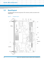
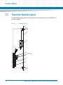
Download MVME4100ET Single Board Computer Installation and Use
Transcript
MVME4100ET Single Board Computer Installation and Use P/N: 6806800K76F June 2014 © Copyright 2014 Artesyn Embedded Technologies, Inc. All rights reserved. Trademarks Artesyn Embedded Technologies, Artesyn and the Artesyn Embedded Technologies logo are trademarks and service marks of Artesyn Embedded Technologies, Inc.© 2014 Artesyn Embedded Technologies, Inc. All other product or service names are the property of their respective owners. Intel® is a trademark or registered trademark of Intel Corporation or its subsidiaries in the United States and other countries. Java™ and all other Java-based marks are trademarks or registered trademarks of Oracle America, Inc. in the U.S. and other countries. Microsoft®, Windows® and Windows Me® are registered trademarks of Microsoft Corporation; and Windows XP™ is a trademark of Microsoft Corporation. PICMG®, CompactPCI®, AdvancedTCA™ and the PICMG, CompactPCI and AdvancedTCA logos are registered trademarks of the PCI Industrial Computer Manufacturers Group. UNIX® is a registered trademark of The Open Group in the United States and other countries. Notice While reasonable efforts have been made to assure the accuracy of this document, Artesyn assumes no liability resulting from any omissions in this document, or from the use of the information obtained therein. Artesyn reserves the right to revise this document and to make changes from time to time in the content hereof without obligation of Artesyn to notify any person of such revision or changes. Electronic versions of this material may be read online, downloaded for personal use, or referenced in another document as a URL to an Artesyn website. The text itself may not be published commercially in print or electronic form, edited, translated, or otherwise altered without the permission of Artesyn. It is possible that this publication may contain reference to or information about Artesyn products (machines and programs), programming, or services that are not available in your country. Such references or information must not be construed to mean that Artesyn intends to announce such Artesyn products, programming, or services in your country. Limited and Restricted Rights Legend If the documentation contained herein is supplied, directly or indirectly, to the U.S. Government, the following notice shall apply unless otherwise agreed to in writing by Artesyn. Use, duplication, or disclosure by the Government is subject to restrictions as set forth in subparagraph (b)(3) of the Rights in Technical Data clause at DFARS 252.227-7013 (Nov. 1995) and of the Rights in Noncommercial Computer Software and Documentation clause at DFARS 252.227-7014 (Jun. 1995). Contact Address Artesyn Embedded Technologies Artesyn Embedded Technologies Marketing Communications Lilienthalstr. 17-19 2900 S. Diablo Way, Suite 190 85579 Neubiberg/Munich Tempe, Arizona 85282 Germany Contents About this Manual . . . . . . . . . . . . . . . . . . . . . . . . . . . . . . . . . . . . . . . . . . . . . . . . . . . . . . . . . . . . . . . . . . . . . . . 11 1 Introduction . . . . . . . . . . . . . . . . . . . . . . . . . . . . . . . . . . . . . . . . . . . . . . . . . . . . . . . . . . . . . . . . . . . . . . . . . 17 1.1 1.2 1.3 1.4 2 Hardware Preparation and Installation . . . . . . . . . . . . . . . . . . . . . . . . . . . . . . . . . . . . . . . . . . . . . . . . . 25 2.1 2.2 2.3 2.4 2.5 2.6 2.7 2.8 3 Features . . . . . . . . . . . . . . . . . . . . . . . . . . . . . . . . . . . . . . . . . . . . . . . . . . . . . . . . . . . . . . . . . . . . . . . . . . . 17 Standard Compliances . . . . . . . . . . . . . . . . . . . . . . . . . . . . . . . . . . . . . . . . . . . . . . . . . . . . . . . . . . . . . . 19 Mechanical Data . . . . . . . . . . . . . . . . . . . . . . . . . . . . . . . . . . . . . . . . . . . . . . . . . . . . . . . . . . . . . . . . . . . 22 Ordering Information . . . . . . . . . . . . . . . . . . . . . . . . . . . . . . . . . . . . . . . . . . . . . . . . . . . . . . . . . . . . . . . 22 1.4.1 Supported Board Models . . . . . . . . . . . . . . . . . . . . . . . . . . . . . . . . . . . . . . . . . . . . . . . . . . . . . . 22 1.4.2 Board Accessories . . . . . . . . . . . . . . . . . . . . . . . . . . . . . . . . . . . . . . . . . . . . . . . . . . . . . . . . . . . . 23 1.4.3 Serial Number Label . . . . . . . . . . . . . . . . . . . . . . . . . . . . . . . . . . . . . . . . . . . . . . . . . . . . . . . . . . 24 Overview . . . . . . . . . . . . . . . . . . . . . . . . . . . . . . . . . . . . . . . . . . . . . . . . . . . . . . . . . . . . . . . . . . . . . . . . . . 25 Unpacking and Inspecting the Board . . . . . . . . . . . . . . . . . . . . . . . . . . . . . . . . . . . . . . . . . . . . . . . . . . 26 Requirements . . . . . . . . . . . . . . . . . . . . . . . . . . . . . . . . . . . . . . . . . . . . . . . . . . . . . . . . . . . . . . . . . . . . . . 27 2.3.1 Environmental Requirements. . . . . . . . . . . . . . . . . . . . . . . . . . . . . . . . . . . . . . . . . . . . . . . . . . 27 2.3.2 Power Requirements . . . . . . . . . . . . . . . . . . . . . . . . . . . . . . . . . . . . . . . . . . . . . . . . . . . . . . . . . 28 2.3.3 Thermal Requirements . . . . . . . . . . . . . . . . . . . . . . . . . . . . . . . . . . . . . . . . . . . . . . . . . . . . . . . 29 2.3.4 Thermally Significant Components . . . . . . . . . . . . . . . . . . . . . . . . . . . . . . . . . . . . . . . . . . . . . 29 2.3.5 Equipment Requirements . . . . . . . . . . . . . . . . . . . . . . . . . . . . . . . . . . . . . . . . . . . . . . . . . . . . . 31 Configuring the Board . . . . . . . . . . . . . . . . . . . . . . . . . . . . . . . . . . . . . . . . . . . . . . . . . . . . . . . . . . . . . . 31 2.4.1 SMT Configuration Switch, S1 . . . . . . . . . . . . . . . . . . . . . . . . . . . . . . . . . . . . . . . . . . . . . . . . . 33 2.4.2 Geographical Address Switch, S2. . . . . . . . . . . . . . . . . . . . . . . . . . . . . . . . . . . . . . . . . . . . . . . 34 Installing Accessories . . . . . . . . . . . . . . . . . . . . . . . . . . . . . . . . . . . . . . . . . . . . . . . . . . . . . . . . . . . . . . . 36 2.5.1 Transition Module. . . . . . . . . . . . . . . . . . . . . . . . . . . . . . . . . . . . . . . . . . . . . . . . . . . . . . . . . . . . 36 2.5.2 PMC . . . . . . . . . . . . . . . . . . . . . . . . . . . . . . . . . . . . . . . . . . . . . . . . . . . . . . . . . . . . . . . . . . . . . . . . 37 2.5.3 XMCspan . . . . . . . . . . . . . . . . . . . . . . . . . . . . . . . . . . . . . . . . . . . . . . . . . . . . . . . . . . . . . . . . . . . 40 Installing and Removing the Board . . . . . . . . . . . . . . . . . . . . . . . . . . . . . . . . . . . . . . . . . . . . . . . . . . . . 40 Completing the Installation . . . . . . . . . . . . . . . . . . . . . . . . . . . . . . . . . . . . . . . . . . . . . . . . . . . . . . . . . . 41 Factory Installed Linux . . . . . . . . . . . . . . . . . . . . . . . . . . . . . . . . . . . . . . . . . . . . . . . . . . . . . . . . . . . . . . 42 Controls, LEDs, and Connectors . . . . . . . . . . . . . . . . . . . . . . . . . . . . . . . . . . . . . . . . . . . . . . . . . . . . . . . . 45 3.1 3.2 Overview . . . . . . . . . . . . . . . . . . . . . . . . . . . . . . . . . . . . . . . . . . . . . . . . . . . . . . . . . . . . . . . . . . . . . . . . . . 45 Board Layout . . . . . . . . . . . . . . . . . . . . . . . . . . . . . . . . . . . . . . . . . . . . . . . . . . . . . . . . . . . . . . . . . . . . . . . 46 MVME4100ET Single Board Computer Installation and Use (6806800K76F) 3 Contents Contents 3.3 3.4 4 Front Panel . . . . . . . . . . . . . . . . . . . . . . . . . . . . . . . . . . . . . . . . . . . . . . . . . . . . . . . . . . . . . . . . . . . . . . . . 47 3.3.1 Reset/Abort Switch. . . . . . . . . . . . . . . . . . . . . . . . . . . . . . . . . . . . . . . . . . . . . . . . . . . . . . . . . . . 48 3.3.2 LEDs . . . . . . . . . . . . . . . . . . . . . . . . . . . . . . . . . . . . . . . . . . . . . . . . . . . . . . . . . . . . . . . . . . . . . . . . 48 3.3.3 Connectors. . . . . . . . . . . . . . . . . . . . . . . . . . . . . . . . . . . . . . . . . . . . . . . . . . . . . . . . . . . . . . . . . . 49 3.3.3.1 XMC Expansion Connector (J6) . . . . . . . . . . . . . . . . . . . . . . . . . . . . . . . . . . . . . . . 50 3.3.3.2 Ethernet Connectors (J4A/J4B) . . . . . . . . . . . . . . . . . . . . . . . . . . . . . . . . . . . . . . . . 52 3.3.3.3 PCI Mezzanine Card (PMC) Connectors (J11 – J14, J21 – J23) . . . . . . . . . . . . . . 52 3.3.3.4 Serial Port Connector (COM1/J1) . . . . . . . . . . . . . . . . . . . . . . . . . . . . . . . . . . . . . . 62 3.3.3.5 VMEbus P1 Connector . . . . . . . . . . . . . . . . . . . . . . . . . . . . . . . . . . . . . . . . . . . . . . . 62 3.3.3.6 VMEbus P2 Connector . . . . . . . . . . . . . . . . . . . . . . . . . . . . . . . . . . . . . . . . . . . . . . . 64 3.3.3.7 MVME721ET PMC I/O Module (PIM) Connectors (J10, J14) . . . . . . . . . . . . . . . 65 Headers . . . . . . . . . . . . . . . . . . . . . . . . . . . . . . . . . . . . . . . . . . . . . . . . . . . . . . . . . . . . . . . . . . . . . . . . . . . 66 3.4.1 Processor COP Header (P4) . . . . . . . . . . . . . . . . . . . . . . . . . . . . . . . . . . . . . . . . . . . . . . . . . . . . 67 3.4.2 Boundary Scan Header (P5). . . . . . . . . . . . . . . . . . . . . . . . . . . . . . . . . . . . . . . . . . . . . . . . . . . . 67 Functional Description . . . . . . . . . . . . . . . . . . . . . . . . . . . . . . . . . . . . . . . . . . . . . . . . . . . . . . . . . . . . . . . . 69 4.1 4.2 4.3 4.4 4.5 4.6 4.7 4.8 Overview . . . . . . . . . . . . . . . . . . . . . . . . . . . . . . . . . . . . . . . . . . . . . . . . . . . . . . . . . . . . . . . . . . . . . . . . . . 69 Block Diagram . . . . . . . . . . . . . . . . . . . . . . . . . . . . . . . . . . . . . . . . . . . . . . . . . . . . . . . . . . . . . . . . . . . . . 70 Processor . . . . . . . . . . . . . . . . . . . . . . . . . . . . . . . . . . . . . . . . . . . . . . . . . . . . . . . . . . . . . . . . . . . . . . . . . . 71 I2C Serial Interface and Devices . . . . . . . . . . . . . . . . . . . . . . . . . . . . . . . . . . . . . . . . . . . . . . . . . . . . . . 71 System Memory . . . . . . . . . . . . . . . . . . . . . . . . . . . . . . . . . . . . . . . . . . . . . . . . . . . . . . . . . . . . . . . . . . . . 72 Timers . . . . . . . . . . . . . . . . . . . . . . . . . . . . . . . . . . . . . . . . . . . . . . . . . . . . . . . . . . . . . . . . . . . . . . . . . . . . 72 Ethernet Interfaces . . . . . . . . . . . . . . . . . . . . . . . . . . . . . . . . . . . . . . . . . . . . . . . . . . . . . . . . . . . . . . . . . 72 Local Bus Interface . . . . . . . . . . . . . . . . . . . . . . . . . . . . . . . . . . . . . . . . . . . . . . . . . . . . . . . . . . . . . . . . . . 73 4.8.1 Flash Memory . . . . . . . . . . . . . . . . . . . . . . . . . . . . . . . . . . . . . . . . . . . . . . . . . . . . . . . . . . . . . . . 73 4.8.2 NVRAM . . . . . . . . . . . . . . . . . . . . . . . . . . . . . . . . . . . . . . . . . . . . . . . . . . . . . . . . . . . . . . . . . . . . . 74 4.8.3 Quad UART (QUART) . . . . . . . . . . . . . . . . . . . . . . . . . . . . . . . . . . . . . . . . . . . . . . . . . . . . . . . . . 74 4.8.4 Control and Timers PLD . . . . . . . . . . . . . . . . . . . . . . . . . . . . . . . . . . . . . . . . . . . . . . . . . . . . . . . 74 4.9 DUART Interface . . . . . . . . . . . . . . . . . . . . . . . . . . . . . . . . . . . . . . . . . . . . . . . . . . . . . . . . . . . . . . . . . . . 75 4.10 PCI-X Port . . . . . . . . . . . . . . . . . . . . . . . . . . . . . . . . . . . . . . . . . . . . . . . . . . . . . . . . . . . . . . . . . . . . . . . . . 75 4.10.1 Tsi148 VME Controller . . . . . . . . . . . . . . . . . . . . . . . . . . . . . . . . . . . . . . . . . . . . . . . . . . . . . . . . 75 4.11 XMC Expansion . . . . . . . . . . . . . . . . . . . . . . . . . . . . . . . . . . . . . . . . . . . . . . . . . . . . . . . . . . . . . . . . . . . . . 75 4.12 Power Supplies . . . . . . . . . . . . . . . . . . . . . . . . . . . . . . . . . . . . . . . . . . . . . . . . . . . . . . . . . . . . . . . . . . . . . 75 4.12.1 Power Sequencing . . . . . . . . . . . . . . . . . . . . . . . . . . . . . . . . . . . . . . . . . . . . . . . . . . . . . . . . . . . 76 4.12.2 Power Supply Monitor . . . . . . . . . . . . . . . . . . . . . . . . . . . . . . . . . . . . . . . . . . . . . . . . . . . . . . . . 76 4 MVME4100ET Single Board Computer Installation and Use (6806800K76F) Contents 4.12.3 Power Supply Filtering and Fusing . . . . . . . . . . . . . . . . . . . . . . . . . . . . . . . . . . . . . . . . . . . . . . 76 4.13 Clock Distribution . . . . . . . . . . . . . . . . . . . . . . . . . . . . . . . . . . . . . . . . . . . . . . . . . . . . . . . . . . . . . . . . . . 76 4.13.1 System Clock . . . . . . . . . . . . . . . . . . . . . . . . . . . . . . . . . . . . . . . . . . . . . . . . . . . . . . . . . . . . . . . . 77 4.13.2 Real Time Clock Input. . . . . . . . . . . . . . . . . . . . . . . . . . . . . . . . . . . . . . . . . . . . . . . . . . . . . . . . . 77 4.13.3 Local Bus Controller Clock Divisor . . . . . . . . . . . . . . . . . . . . . . . . . . . . . . . . . . . . . . . . . . . . . . 77 4.14 Reset Control Logic . . . . . . . . . . . . . . . . . . . . . . . . . . . . . . . . . . . . . . . . . . . . . . . . . . . . . . . . . . . . . . . . . 77 4.15 Real Time Clock Battery . . . . . . . . . . . . . . . . . . . . . . . . . . . . . . . . . . . . . . . . . . . . . . . . . . . . . . . . . . . . . 78 4.16 Debug Support . . . . . . . . . . . . . . . . . . . . . . . . . . . . . . . . . . . . . . . . . . . . . . . . . . . . . . . . . . . . . . . . . . . . . 78 5 Transition Module . . . . . . . . . . . . . . . . . . . . . . . . . . . . . . . . . . . . . . . . . . . . . . . . . . . . . . . . . . . . . . . . . . . . 79 5.1 5.2 5.3 5.4 5.5 5.6 6 Overview . . . . . . . . . . . . . . . . . . . . . . . . . . . . . . . . . . . . . . . . . . . . . . . . . . . . . . . . . . . . . . . . . . . . . . . . . . 79 Transition Module Layout . . . . . . . . . . . . . . . . . . . . . . . . . . . . . . . . . . . . . . . . . . . . . . . . . . . . . . . . . . . . 80 Features . . . . . . . . . . . . . . . . . . . . . . . . . . . . . . . . . . . . . . . . . . . . . . . . . . . . . . . . . . . . . . . . . . . . . . . . . . . 81 SEEPROM Address Switch, S1 . . . . . . . . . . . . . . . . . . . . . . . . . . . . . . . . . . . . . . . . . . . . . . . . . . . . . . . . 82 Rear Panel Connectors . . . . . . . . . . . . . . . . . . . . . . . . . . . . . . . . . . . . . . . . . . . . . . . . . . . . . . . . . . . . . . 83 PMC Input/Output Module . . . . . . . . . . . . . . . . . . . . . . . . . . . . . . . . . . . . . . . . . . . . . . . . . . . . . . . . . . 85 MOTLoad Firmware. . . . . . . . . . . . . . . . . . . . . . . . . . . . . . . . . . . . . . . . . . . . . . . . . . . . . . . . . . . . . . . . . . . 87 6.1 6.2 6.3 6.4 6.5 Overview . . . . . . . . . . . . . . . . . . . . . . . . . . . . . . . . . . . . . . . . . . . . . . . . . . . . . . . . . . . . . . . . . . . . . . . . . . 87 Implementation and Memory Requirements . . . . . . . . . . . . . . . . . . . . . . . . . . . . . . . . . . . . . . . . . . . 87 MOTLoad Commands . . . . . . . . . . . . . . . . . . . . . . . . . . . . . . . . . . . . . . . . . . . . . . . . . . . . . . . . . . . . . . . 87 6.3.1 Utilities . . . . . . . . . . . . . . . . . . . . . . . . . . . . . . . . . . . . . . . . . . . . . . . . . . . . . . . . . . . . . . . . . . . . . 87 6.3.2 Tests . . . . . . . . . . . . . . . . . . . . . . . . . . . . . . . . . . . . . . . . . . . . . . . . . . . . . . . . . . . . . . . . . . . . . . . 88 6.3.3 Command List . . . . . . . . . . . . . . . . . . . . . . . . . . . . . . . . . . . . . . . . . . . . . . . . . . . . . . . . . . . . . . . 89 Using the Command Line Interface . . . . . . . . . . . . . . . . . . . . . . . . . . . . . . . . . . . . . . . . . . . . . . . . . . . 94 6.4.1 Rules . . . . . . . . . . . . . . . . . . . . . . . . . . . . . . . . . . . . . . . . . . . . . . . . . . . . . . . . . . . . . . . . . . . . . . . 96 6.4.2 Help . . . . . . . . . . . . . . . . . . . . . . . . . . . . . . . . . . . . . . . . . . . . . . . . . . . . . . . . . . . . . . . . . . . . . . . . 96 Firmware Settings . . . . . . . . . . . . . . . . . . . . . . . . . . . . . . . . . . . . . . . . . . . . . . . . . . . . . . . . . . . . . . . . . . 97 6.5.1 Default VME Settings . . . . . . . . . . . . . . . . . . . . . . . . . . . . . . . . . . . . . . . . . . . . . . . . . . . . . . . . . 97 6.5.2 Control Register/Control Status Register Settings . . . . . . . . . . . . . . . . . . . . . . . . . . . . . . . 101 6.5.3 Displaying VME Settings . . . . . . . . . . . . . . . . . . . . . . . . . . . . . . . . . . . . . . . . . . . . . . . . . . . . . 101 6.5.4 Editing VME Settings . . . . . . . . . . . . . . . . . . . . . . . . . . . . . . . . . . . . . . . . . . . . . . . . . . . . . . . . 102 6.5.5 Deleting VME Settings . . . . . . . . . . . . . . . . . . . . . . . . . . . . . . . . . . . . . . . . . . . . . . . . . . . . . . . 102 6.5.6 Restoring Default VME Settings . . . . . . . . . . . . . . . . . . . . . . . . . . . . . . . . . . . . . . . . . . . . . . . 103 MVME4100ET Single Board Computer Installation and Use (6806800K76F) 5 Contents Contents 6.6 6.7 6.8 A Battery Exchange. . . . . . . . . . . . . . . . . . . . . . . . . . . . . . . . . . . . . . . . . . . . . . . . . . . . . . . . . . . . . . . . . . . . 111 A.1 B Remote Start . . . . . . . . . . . . . . . . . . . . . . . . . . . . . . . . . . . . . . . . . . . . . . . . . . . . . . . . . . . . . . . . . . . . . 103 Boot Images . . . . . . . . . . . . . . . . . . . . . . . . . . . . . . . . . . . . . . . . . . . . . . . . . . . . . . . . . . . . . . . . . . . . . . 104 6.7.1 Checksum Algorithm . . . . . . . . . . . . . . . . . . . . . . . . . . . . . . . . . . . . . . . . . . . . . . . . . . . . . . . . 105 6.7.2 Image Flags . . . . . . . . . . . . . . . . . . . . . . . . . . . . . . . . . . . . . . . . . . . . . . . . . . . . . . . . . . . . . . . . 106 6.7.3 User Images . . . . . . . . . . . . . . . . . . . . . . . . . . . . . . . . . . . . . . . . . . . . . . . . . . . . . . . . . . . . . . . . 107 6.7.4 Alternate Boot Data Structure . . . . . . . . . . . . . . . . . . . . . . . . . . . . . . . . . . . . . . . . . . . . . . . . 107 6.7.5 Alternate Boot Images and Safe Start . . . . . . . . . . . . . . . . . . . . . . . . . . . . . . . . . . . . . . . . . . 108 6.7.6 Boot Image Firmware Scan . . . . . . . . . . . . . . . . . . . . . . . . . . . . . . . . . . . . . . . . . . . . . . . . . . . 108 Startup Sequence . . . . . . . . . . . . . . . . . . . . . . . . . . . . . . . . . . . . . . . . . . . . . . . . . . . . . . . . . . . . . . . . . 109 Battery Exchange . . . . . . . . . . . . . . . . . . . . . . . . . . . . . . . . . . . . . . . . . . . . . . . . . . . . . . . . . . . . . . . . . . 111 Related Documentation . . . . . . . . . . . . . . . . . . . . . . . . . . . . . . . . . . . . . . . . . . . . . . . . . . . . . . . . . . . . . . 115 B.1 B.2 B.3 Artesyn Embedded Technologies - Embedded Computing Documentation . . . . . . . . . . . . . . . 115 Manufacturers’ Documents . . . . . . . . . . . . . . . . . . . . . . . . . . . . . . . . . . . . . . . . . . . . . . . . . . . . . . . . . 115 Related Specifications . . . . . . . . . . . . . . . . . . . . . . . . . . . . . . . . . . . . . . . . . . . . . . . . . . . . . . . . . . . . . . 118 Safety Notes . . . . . . . . . . . . . . . . . . . . . . . . . . . . . . . . . . . . . . . . . . . . . . . . . . . . . . . . . . . . . . . . . . . . . . . . . . . . 121 Sicherheitshinweise . . . . . . . . . . . . . . . . . . . . . . . . . . . . . . . . . . . . . . . . . . . . . . . . . . . . . . . . . . . . . . . . . . . . . 125 6 MVME4100ET Single Board Computer Installation and Use (6806800K76F) List of Tables Table 1-1 Table 1-2 Table 1-3 Table 1-4 Table 1-5 Table 2-1 Table 2-2 Table 2-3 Table 2-4 Table 2-5 Table 2-6 Table 3-1 Table 3-2 Table 3-3 Table 3-4 Table 3-5 Table 3-6 Table 3-7 Table 3-8 Table 3-9 Table 3-10 Table 3-11 Table 3-12 Table 3-13 Table 3-14 Table 3-15 Table 3-16 Table 3-17 Table 4-1 Table 5-1 Table 5-2 Table 5-3 Table 5-4 Table 5-5 Table 6-1 Table 6-2 Features List . . . . . . . . . . . . . . . . . . . . . . . . . . . . . . . . . . . . . . . . . . . . . . . . . . . . . . . . . . . . . . . . . . . 17 Board Standard Compliances . . . . . . . . . . . . . . . . . . . . . . . . . . . . . . . . . . . . . . . . . . . . . . . . . . . . 19 Mechanical Data . . . . . . . . . . . . . . . . . . . . . . . . . . . . . . . . . . . . . . . . . . . . . . . . . . . . . . . . . . . . . . . 22 Board Variants . . . . . . . . . . . . . . . . . . . . . . . . . . . . . . . . . . . . . . . . . . . . . . . . . . . . . . . . . . . . . . . . . 22 Board Accessories . . . . . . . . . . . . . . . . . . . . . . . . . . . . . . . . . . . . . . . . . . . . . . . . . . . . . . . . . . . . . . 23 Startup Overview . . . . . . . . . . . . . . . . . . . . . . . . . . . . . . . . . . . . . . . . . . . . . . . . . . . . . . . . . . . . . . 25 MVME4100ET Specifications . . . . . . . . . . . . . . . . . . . . . . . . . . . . . . . . . . . . . . . . . . . . . . . . . . . . 27 Power Requirements . . . . . . . . . . . . . . . . . . . . . . . . . . . . . . . . . . . . . . . . . . . . . . . . . . . . . . . . . . . 28 Thermally Significant Components . . . . . . . . . . . . . . . . . . . . . . . . . . . . . . . . . . . . . . . . . . . . . . . 29 Configuration Switch Settings (S1) . . . . . . . . . . . . . . . . . . . . . . . . . . . . . . . . . . . . . . . . . . . . . . . 34 Geographical Address Switch Settings . . . . . . . . . . . . . . . . . . . . . . . . . . . . . . . . . . . . . . . . . . . . 35 Front Panel LEDs . . . . . . . . . . . . . . . . . . . . . . . . . . . . . . . . . . . . . . . . . . . . . . . . . . . . . . . . . . . . . . . 48 Base Board Connectors . . . . . . . . . . . . . . . . . . . . . . . . . . . . . . . . . . . . . . . . . . . . . . . . . . . . . . . . . 49 XMC Expansion Connector (J6) Pin Assignments . . . . . . . . . . . . . . . . . . . . . . . . . . . . . . . . . . . 50 Ethernet Connectors (J4A/J4B) Pin Assignments . . . . . . . . . . . . . . . . . . . . . . . . . . . . . . . . . . . 52 PMC Slot 1 Connector (J11) Pin Assignments . . . . . . . . . . . . . . . . . . . . . . . . . . . . . . . . . . . . . . 52 PMC Slot 1 Connector (J12) Pin Assignments . . . . . . . . . . . . . . . . . . . . . . . . . . . . . . . . . . . . . . 54 PMC Slot 1 Connector (J13) Pin Assignments . . . . . . . . . . . . . . . . . . . . . . . . . . . . . . . . . . . . . . 55 PMC Slot 1 Connector (J14) Pin Assignments . . . . . . . . . . . . . . . . . . . . . . . . . . . . . . . . . . . . . . 56 PMC Slot 2 Connector (J21) Pin Assignments . . . . . . . . . . . . . . . . . . . . . . . . . . . . . . . . . . . . . . 58 PMC Slot 2 Connector (J22) Pin Assignments . . . . . . . . . . . . . . . . . . . . . . . . . . . . . . . . . . . . . . 59 PMC Slot 2 Connector (J23) Pin Assignments . . . . . . . . . . . . . . . . . . . . . . . . . . . . . . . . . . . . . . 60 COM1 Port Connector Pin Assignments . . . . . . . . . . . . . . . . . . . . . . . . . . . . . . . . . . . . . . . . . . . 62 VMEbus P1 Connector Pin Assignments . . . . . . . . . . . . . . . . . . . . . . . . . . . . . . . . . . . . . . . . . . . 62 VME P2 Connector Pinouts . . . . . . . . . . . . . . . . . . . . . . . . . . . . . . . . . . . . . . . . . . . . . . . . . . . . . . 64 MVME721 Host I/O Connector (J10) Pin Assignments . . . . . . . . . . . . . . . . . . . . . . . . . . . . . . . 65 Processor COP Header (P4) Pin Assignments . . . . . . . . . . . . . . . . . . . . . . . . . . . . . . . . . . . . . . . 67 Boundary Scan Header (P5) Pin Assignments . . . . . . . . . . . . . . . . . . . . . . . . . . . . . . . . . . . . . . 67 Clock Frequencies . . . . . . . . . . . . . . . . . . . . . . . . . . . . . . . . . . . . . . . . . . . . . . . . . . . . . . . . . . . . . . 77 Transition Module Features . . . . . . . . . . . . . . . . . . . . . . . . . . . . . . . . . . . . . . . . . . . . . . . . . . . . . . 81 SEEPROM Address Switch Assignments (RTM) . . . . . . . . . . . . . . . . . . . . . . . . . . . . . . . . . . . . . 82 Switch Settings and Device Addresses . . . . . . . . . . . . . . . . . . . . . . . . . . . . . . . . . . . . . . . . . . . . 82 Transition Module Connectors . . . . . . . . . . . . . . . . . . . . . . . . . . . . . . . . . . . . . . . . . . . . . . . . . . . 83 Transition Module LEDs . . . . . . . . . . . . . . . . . . . . . . . . . . . . . . . . . . . . . . . . . . . . . . . . . . . . . . . . . 85 MOTLoad Commands . . . . . . . . . . . . . . . . . . . . . . . . . . . . . . . . . . . . . . . . . . . . . . . . . . . . . . . . . . 89 MOTLoad Image Flags . . . . . . . . . . . . . . . . . . . . . . . . . . . . . . . . . . . . . . . . . . . . . . . . . . . . . . . . . 106 MVME4100ET Single Board Computer Installation and Use (6806800K76F) 7 List of Tables Table B-1 Table B-2 Table B-3 8 Artesyn Embedded Technologies - Embedded Computing Publications . . . . . . . . . . . . . .115 Manufacturer’s Publications . . . . . . . . . . . . . . . . . . . . . . . . . . . . . . . . . . . . . . . . . . . . . . . . . . . .115 Related Specifications . . . . . . . . . . . . . . . . . . . . . . . . . . . . . . . . . . . . . . . . . . . . . . . . . . . . . . . . .118 MVME4100ET Single Board Computer Installation and Use (6806800K76F) List of Figures Figure 1-1 Figure 1-2 Figure 2-1 Figure 2-2 Figure 2-3 Figure 2-4 Figure 2-5 Figure 2-6 Figure 3-1 Figure 3-2 Figure 4-1 Figure 5-1 Figure 5-2 Figure 5-3 Figure 5-4 Figure 5-5 Figure A-1 Declaration of Conformity . . . . . . . . . . . . . . . . . . . . . . . . . . . . . . . . . . . . . . . . . . . . . . . . 21 Serial Number Label Location . . . . . . . . . . . . . . . . . . . . . . . . . . . . . . . . . . . . . . . . . . . . . 24 Primary Side Thermally Significant Components . . . . . . . . . . . . . . . . . . . . . . . . . . . . 30 Secondary Side Thermally Significant Components . . . . . . . . . . . . . . . . . . . . . . . . . . 31 Switch Locations . . . . . . . . . . . . . . . . . . . . . . . . . . . . . . . . . . . . . . . . . . . . . . . . . . . . . . . . 32 SMT Configuration Switch Position . . . . . . . . . . . . . . . . . . . . . . . . . . . . . . . . . . . . . . . . 33 Geographical Address Switch Position . . . . . . . . . . . . . . . . . . . . . . . . . . . . . . . . . . . . . 35 Typical Placement of a PMC Module on a VME Module . . . . . . . . . . . . . . . . . . . . . . . 39 Component Layout . . . . . . . . . . . . . . . . . . . . . . . . . . . . . . . . . . . . . . . . . . . . . . . . . . . . . . 46 Front Panel LEDs, Connectors, Switch . . . . . . . . . . . . . . . . . . . . . . . . . . . . . . . . . . . . . . 47 Block Diagram . . . . . . . . . . . . . . . . . . . . . . . . . . . . . . . . . . . . . . . . . . . . . . . . . . . . . . . . . . 70 Component Layout . . . . . . . . . . . . . . . . . . . . . . . . . . . . . . . . . . . . . . . . . . . . . . . . . . . . . . 80 Block Diagram . . . . . . . . . . . . . . . . . . . . . . . . . . . . . . . . . . . . . . . . . . . . . . . . . . . . . . . . . . 81 S1 Switch Positions . . . . . . . . . . . . . . . . . . . . . . . . . . . . . . . . . . . . . . . . . . . . . . . . . . . . . . 82 Rear Panel Connectors and LEDs . . . . . . . . . . . . . . . . . . . . . . . . . . . . . . . . . . . . . . . . . . 84 Installing the PIM . . . . . . . . . . . . . . . . . . . . . . . . . . . . . . . . . . . . . . . . . . . . . . . . . . . . . . . 86 Battery Location . . . . . . . . . . . . . . . . . . . . . . . . . . . . . . . . . . . . . . . . . . . . . . . . . . . . . . . 111 MVME4100ET Single Board Computer Installation and Use (6806800K76F) 9 List of Figures 10 MVME4100ET Single Board Computer Installation and Use (6806800K76F) About this Manual Overview of Contents This manual provides the information required to install and configure an MVME4100ET Single Board Computer. Additionally, this manual provides specific preparation and installation information and data applicable to the board. The MVME4100ET Single Board Computer, with the Freescale MPC8548E System on Chip (SoC) processor, provides a high-performance, cost-effective continuation for currently deployed VME infrastructure. This manual is divided into the following chapters and appendices: Chapter 1, Introduction, lists the features of the MVME4100ET base board, standard compliances, and model numbers for boards and accessories. Chapter 2, Hardware Preparation and Installation, includes a description of the MVME4100ET, unpacking instructions, environmental, thermal, and power requirements, and how to prepare and install the base board, transition module, and PMC module. Chapter 3, Controls, LEDs, and Connectors, provides an illustration of the board components and front panel details. This chapter also provides descriptions for the front panel LEDs and connectors. Chapter 4, Functional Description, describes the major features of the MVME4100ET base board. These descriptions include both programming and hardware characteristics of major components. Chapter 5, Transition Module, describes the MVME721ET transition module used with the MVME4100ET. Chapter 6, MOTLoad Firmware, describes the role, process, and commands employed by the MVME4100ET diagnostic and initialization firmware MOTLoad. This chapter also briefly describes how to use the debugger commands. Appendix A, Battery Exchange, describes the procedure for replacing a battery. Appendix B, Related Documentation, provides a list of publications, manufacturer’s documents, and related industry specification for this product. Safety Notes summarizes the safety instructions in the manual. Sicherheitshinweise is a German translation of the Safety Notes chapter. MVME4100ET Single Board Computer Installation and Use (6806800K76F) 11 About this Manual About this Manual Abbreviations This document uses the following abbreviations: 12 Term Meaning A Ampere ANSI American National Standard Institute BLT Block Transfer CFM Cubic Feet per Minute CMC Common Mezzanine Card COM Communications COP Common On-chip Processor CPU Central Processing Unit DDR Double Data Rate °C Degree Celsius DMA Direct Memory Access DRAM Dynamic Random Access Memory DUART Dual Universal Asynchronous Receiver/Transmitter ECC Error Correction Code EEPROM Electrically Erasable Programmable Read-Only Memory FCC Federal Communications Commission FIFO First In First Out GB Gigabytes Gbit Gigabit Gbps Gigabits Per Second GPCM General Purpose Chip select Machine H/W Hardware IEEE Institute of Electrical and Electronics Engineers I2C Inter IC JTAG Joint Test Access Group MVME4100ET Single Board Computer Installation and Use (6806800K76F) About this Manual Term Meaning KB Kilobytes KBAUD Kilo Baud LBC Local Bus Controller LED Light Emitting Diode MB Megabytes Mbps Megabits Per Second MHz Megahertz NAND (Not and) Flash that is used for storage NOR (Not or) Flash that is used for executing code OS Operating System PCI Peripheral Component Interconnect PCI-X Peripheral Component Interconnect -X PIC Programmable Interrupt Controller PIM PCI Mezzanine Card Input/Output Module PMC PCI Mezzanine Card (IEEE P1386.1) PLD Programmable Logic Device QUART Quad Universal Asynchronous Receiver/Transmitter RAM Random Access Memory RGMII Reduced Gigabit Media Independent Interface RTC Real-Time Clock RTM Rear Transition Module SBC Single Board Computer SDRAM Synchronous Dynamic Random Access Memory SMT Surface Mount Technology SODIMM Small-Outline Dual In-line Memory Module SPD Serial Presence Detect SoC System-on-Chip SRAM Static Random Access Memory MVME4100ET Single Board Computer Installation and Use (6806800K76F) 13 About this Manual About this Manual Term Meaning S/W Software TSEC Three-Speed Ethernet Controller 2eSST Two edge Source Synchronous Transfer UART Universal Asynchronous Receiver/Transmitter V Volts VIO Input/Output Voltage VITA VMEbus International Trade Association VME Versa Module Eurocard VPD Vital Product Data W Watts Conventions The following table describes the conventions used throughout this manual. 14 Notation Description 0x00000000 Typical notation for hexadecimal numbers (digits are 0 through F), for example used for addresses and offsets 0b0000 Same for binary numbers (digits are 0 and 1) bold Used to emphasize a word Screen Used for on-screen output and code related elements or commands in body text Courier + Bold Used to characterize user input and to separate it from system output Reference Used for references and for table and figure descriptions File > Exit Notation for selecting a submenu <text> Notation for variables and keys [text] Notation for software buttons to click on the screen and parameter description MVME4100ET Single Board Computer Installation and Use (6806800K76F) About this Manual Notation Description ... Repeated item for example node 1, node 2, ..., node 12 . Omission of information from example/command that is not necessary at the time being . . .. Ranges, for example: 0..4 means one of the integers 0,1,2,3, and 4 (used in registers) | Logical OR Indicates a hazardous situation which, if not avoided, could result in death or serious injury Indicates a hazardous situation which, if not avoided, may result in minor or moderate injury Indicates a property damage message No danger encountered. Pay attention to important information MVME4100ET Single Board Computer Installation and Use (6806800K76F) 15 About this Manual About this Manual Summary of Changes 16 Part Number Publication Date Description 6806800K76A July 2010 Initial version 6806800K76B March 2011 Minor correction to Factory Installed Linux on page 42. 6806800K76C July 2011 Updated Table "MVME4100ET Specifications" on page 27. 6806800K76D August 2011 Updated Safety Notes on page 121 and Sicherheitshinweise on page 125. 6806800K76E December 2012 Updated Standard Compliances on page 19. 6806800K76F June 2014 Re- branded to Artesyn template. MVME4100ET Single Board Computer Installation and Use (6806800K76F) Chapter 1 Introduction 1.1 Features The MVME4100ET Single Board Computer is a VMEbus board based on the MPC8548E Integrated Processor. It is a full 6U board and occupies a single VME card slot with PMC cards installed. The MVME4100ET is compliant with the VITA standards VMEbus, 2eSST, and PCI-X as listed in Appendix B, Related Documentation. Target applications for this board are medical imaging, industrial control, radar/sonar, and test and measure. Table 1-1 Features List Function Features Processor / Host Controller / Memory Controller One MPC8548E Integrated Processor One e500 core with integrated L2 Core frequency of 1.3 GHz One integrated four channel DMA controller One integrated PCI-E interface One integrated PCI-X interface Four integrated 10/100/1000 Ethernet controllers One integrated DUART Two integrated I2C controllers One integrated Programmable Interrupt Controller One integrated Local Bus Controller One integrated DDR2 SDRAM controller System Memory One DDR2 SO-CDIMM for SDRAM with ECC 2 GBytes Up to DDR533 I2C One 8 KB VPD serial EEPROM Two 64 KB user configuration serial EEPROMs One Real Time Clock (RTC) with removable battery Dual temperature sensor One SPD for memory on SO-CDIMM Connection to XMCspan and rear transition module MVME4100ET Single Board Computer Installation and Use (6806800K76F) 17 Introduction Table 1-1 Features List (continued) Function Features Flash 128 MB soldered NOR flash with two alternate 1 MB boot sectors selectable via hardware switch H/W switch or S/W bit write protection for entire logical bank 4 GB NAND flash NVRAM One 512 KB MRAM extended temperature range PCI_E 8X Port to XMC Expansion I/O One front panel mini DB-9 connector for front I/O: one serial channel Two front panel RJ-45 connectors with integrated LEDs for front I/O: two 10/100/1000 Ethernet channels PMC site 1 front I/O and rear P2 I/O PMC site 2 front I/O Ethernet Four 10/100/1000 MPC8548E Ethernet channels: two front panel Ethernet connectors and two channels for rear P2 I/O Serial Interface One 16550-compatible, 9.6 to 115.2 Kbaud, MPC8548E, asynchronous serial channel: one channel for front panel I/O One quad UART (QUART) controller to provide four 16550compatible, 9.6 to 115.2 Kbaud, asynchronous serial channels: four channels for rear P2 I/O Timers Four 32-bit MPC8548E timers Four 32-bit timers in a PLD Watchdog Timer One watchdog timer in a PLD VME Interface VME64 (ANSI/VITA 1-1994) compliant (3 row backplane 96-pin VME connector) VME64 Extensions (ANSI/VITA 1.1-1997) compliant (5 row backplane 160-pin VME connector) 2eSST (ANSI/VITA 1.5-2003) compliant ANSI/VITA 1.7-2003 compliant (Increased Current Level for 96 pin & 160 pin DIN/IEC Connector Standard) VITA 41.0, version 0.9 compliant Two five-row P1 and P2 backplane connectors One Tsi148 VMEbus controller Form Factor 18 Standard 6U VME, one slot MVME4100ET Single Board Computer Installation and Use (6806800K76F) Introduction Table 1-1 Features List (continued) Function Features Miscellaneous One front panel RESET/ABORT switch Six front panel status indicators: Two 10/100/1000 Ethernet link/speed and activity (4 total) Board fail User S/W controlled LED Planar status indicators One standard 16-pin COP header One standard 20-pin JTAG header Boundary scan support Switches for VME geographical addressing in a three-row backplane Software Support VxWorks OS support Linux OS support 1.2 Standard Compliances The MVME4100ET is designed to be CE compliant and to meet the following standard requirements. Table 1-2 Board Standard Compliances Standard Description UL 60950-1 Safety Requirements (legal) EN 60950-1 IEC 60950-1 CAN/CSA C22.2 No 60950-1 MVME4100ET Single Board Computer Installation and Use (6806800K76F) 19 Introduction Table 1-2 Board Standard Compliances (continued) Standard Description CISPR 22 EMC requirements (legal) on system level (predefined Artesyn system) CISPR 24 EN 55022 EN 55024 FCC Part 15 Industry Canada ICES-003 VCCI Japan AS/NZS CISPR 22 EN 300 386 NEBS Standard GR-1089 CORE NEBS Standard GR-63-CORE Environmental Requirements ETSI EN 300 019 series Directive 2011/65/EU 20 Directive on the restriction of the use of certain hazardous substances in electrical and electronic equipment (RoHS) MVME4100ET Single Board Computer Installation and Use (6806800K76F) Introduction Figure 1-1 Declaration of Conformity EC Declaration of Conformity According to EN 17050-1:2004 Manufacturer’s Name: Artesyn Embedded Technologies Embedded Computing Manufacturer’s Address: Zhongshan General Carton Box Factory Co. Ltd. No 62, Qi Guan Road West, Shiqi District, 528400 Zhongshan City Guangdong, PRC Declares that the following product, in accordance with the requirements of 2004/108/EC, 2006/95/EC, 2011/65/ EU and their amending directives, Product: MVME4100ET Extended Temperature VMEbus Single Board Computer Series Model Name/Number: MVME4100ET-0171, MVME4100ET-0173, MVME4100ET-0173-M has been designed and manufactured to the following specifications: EN55022: 2006 EN55024 (A1: 2001 + A2: 2003): 1998 2011/65/EU RoHS Directive As manufacturer we hereby declare that the product named above has been designed to comply with the relevant sections of the above referenced specifications. This product complies with the essential health and safety requirements of the above specified directives. We have an internal production control system that ensures compliance between the manufactured products and the technical documentation. ___________________________________________________ Tom Tuttle, Manager, Product Testing Services MVME4100ET Single Board Computer Installation and Use (6806800K76F) ___06/17/2014______ Date (MM/DD/YYYY) 21 Introduction 1.3 Mechanical Data This section provides details on the board’s mechanical data. Table 1-3 Mechanical Data 1.4 Characteristic Value Dimensions (D x W x H) 6U, 4HP wide, (233.4 mm x 160 mm x 19.8 mm) Weight 0.453 kg Ordering Information While ordering board variants or board accessories, use the order numbers given in the following tables. 1.4.1 Supported Board Models The MVME4100ET Single Board Computer is available in the configurations shown below. Table 1-4 Board Variants 22 Marketing Number Processor MVME4100ET-0171 1.3GHZ MPC8548E, 4G NAND FLASH, 2G DDR2-533 SO-CDIMM, SCANBE at -40C to +71c operating temperature MVME4100ET-0173 1.3GHZ MPC8548E, 4G NAND FLASH, 2G DDR2-533 SO-CDIMM, IEEE at -40C to +71c operating temperature MVME4100ET Single Board Computer Installation and Use (6806800K76F) Introduction 1.4.2 Board Accessories The following table lists the available expansion and transition modules for the MVME4100ET. Table 1-5 Board Accessories Model Number Description MVME721ET-101 Rear Transition Module at -40C to +71c operating temperature MVME721ET-102 RTM with the SCANBE handles XMCSPAN-001 XMC Expansion, IEEE handles XMCSPAN-002 XMC Expansion, SCANBE handles The IPMC712 and IPMC761 I/O modules are not supported on the MVME4100ET. MVME4100ET Single Board Computer Installation and Use (6806800K76F) 23 Introduction 1.4.3 Serial Number Label You can find the serial number of the product on a label that is located on the PCB close to the front panel. The following figure shows a sample label and its location. The actual label on your product may vary in content and location. Figure 1-2 24 Serial Number Label Location MVME4100ET Single Board Computer Installation and Use (6806800K76F) Chapter 2 Hardware Preparation and Installation 2.1 Overview This chapter provides startup and safety instructions related to this product, and hardware preparation instruction that includes default switch settings. System considerations and installation instructions for the base board, PMC, and transition module are also described in this chapter. A fully implemented MVME4100ET consists of the following along with the base board: Two single-wide or one double-wide PCI Mezzanine Card (PMC) slot for added versatility. One transition module for support of the mapped I/O from the MVME4100ET base board to the P2 connector. Up to two optional XMCspan cards. The following table lists the tasks that you need to do before you can use this board. Read this entire chapter, including all Cautions and Warnings, before you begin. Table 2-1 Startup Overview Task Page Unpack the hardware. Unpacking and Inspecting the Board on page 26 Configure the hardware by setting jumpers on the board and RTM. Configuring the Board on page 31 and SEEPROM Address Switch, S1 on page 82 Install the MVME721ET transition module in the chassis. Transition Module on page 36 Install PMC module (if required). Installing Accessories on page 36 Install XMCspan module (if required). XMCspan Installation and Use manual (6806800H03) Install the MVME4100ET in the chassis. Installing and Removing the Board on page 40 Attach cabling and apply power. Completing the Installation on page 41 Install PIM on transition module (if required). PMC Input/Output Module on page 85 Ensure that the firmware initializes the MVME4100ET Chapter 6, MOTLoad Firmware Initialize the board Chapter 6, MOTLoad Firmware Examine and/or change environmental parameters. MVME4100ET Single Board Computer Programmer’s Reference MVME4100ET Single Board Computer Installation and Use (6806800K76F) 25 Hardware Preparation and Installation Table 2-1 Startup Overview (continued) 2.2 Task Page Program the board as needed for your applications. MVME4100ET Single Board Computer Programmer’s Reference Unpacking and Inspecting the Board Read all notices and cautions prior to unpacking the product. Damage of Circuits Electrostatic discharge and incorrect installation and removal can damage circuits or shorten their life. Before touching the board or electronic components, make sure that you are working in an ESD-safe environment. Shipment Inspection inspect the shipment as follows: 1. Verify that you have received all items of your shipment. 2. Check for damage and report any damage or differences to customer service. 3. Remove the desiccant bag shipped together with the board and dispose of it according to your country’s legislation. The product is thoroughly inspected before shipment. If any damage occurred during transportation or any items are missing, contact customer service immediately. 26 MVME4100ET Single Board Computer Installation and Use (6806800K76F) Hardware Preparation and Installation 2.3 Requirements Make sure that the board, when operated in your particular system configuration, meets the requirements specified in the next sections. 2.3.1 Environmental Requirements The following table lists the currently available specifications for the environmental characteristics of the MVME4100ET. A complete functional description of the MVME4100ET base board is available in Chapter 4, Functional Description. Operating temperatures refer to the temperature of the air circulating around the board and not to the component temperature. Table 2-2 MVME4100ET Specifications Characteristics Operating Cooling Method Force Air Operating Temperature -40C to +71C Storage Temperature -50C to +100C Temperature Transition Time Operational temperature transition rate 0.5c/minute Vibration Swept sine: 1.0 g from 5.0 to 200 Hz Sweep rate: 0.25 octaves/minute Humidity Designed to operate up to 100% relative humidity, Non condensing The RTC field removable battery should be removed, if MVME4100ET has to be stored beyond its operational temperature range. MVME4100ET Single Board Computer Installation and Use (6806800K76F) 27 Hardware Preparation and Installation Product Damage High humidity and condensation on the board surface causes short circuits. Do not operate the board outside the specified environmental limits. Make sure the board is completely dry and there is no moisture on any surface before applying power. 2.3.2 Power Requirements Up to 90 W (18 A at 5 V) of power can be supplied to the board in a 5-row backplane. 70 W (14 A at 5 V) can be supplied in a 3-row backplane. The board requires 18 W to 22 W (3.6 A to 4.4 A at 5 V) to operate. The remainder is available to the PMC site, but you have to make sure to not exceed 10 A (33 W) on 3.3 V. The table below provides an estimate of the typical and maximum power required. Table 2-3 Power Requirements Board Variant Power MVME4100ET-0171 Typical: 18 W at +5 V Maximum: 22 W at +5 V MVME4100ET-0173 Typical: 18 W at +5 V Maximum: 22 W at +5 V The following table shows the power available when the MVME4100ET is installed in either a 3row or 5-row chassis and when PMCs are present. Chassis Type Available Power Power With PMCs 3-Row 70 W maximum Below 70 W1 5-Row 90 W maximum Below 90 W1 1. Keep below power limit. Cooling limitations must be considered. 28 MVME4100ET Single Board Computer Installation and Use (6806800K76F) Hardware Preparation and Installation 2.3.3 Thermal Requirements The MVME4100ET module requires a minimum air flow of 14 CFM uniformly distributed across the board, with the airflow traveling from the heat sink to the PMC2 site, when operating at a 71°C (160 °F) ambient temperature. 2.3.4 Thermally Significant Components The following table summarizes components that exhibit significant temperature rises. These are the components that should be monitored in order to assess thermal performance. The table also supplies the component reference designator and the maximum allowable operating temperature. You can find components on the board by their reference designators as shown in Figure 2-1 and Figure 2-2. Versions of the board that are not fully populated may not contain some of these components. The preferred measurement location for a component may be junction or case as specified in the below table. Junction temperature refers to the temperature measured by an on-chip thermal device. Case temperature refers to the temperature at the top, center surface of the component. Table 2-4 Thermally Significant Components Reference Designator Generic Description Maximum Allowable Component Temperature Measurement Location U12 Processor 105 °C (+221 °F) Junction U4, U27 Gb Ethernet Transceivers 125 °C (+257 °F) Junction U66 MRAM 115 °C (+239 °F) Junction U24 VME Bridge 122 °C (+251.6 °F) Junction U22, U25 PCI-X to PCI-X Bridge 125 °C (+257 °F) Junction U67 PLD 90 °C (+194 °F) Junction U21 CPLD 85 °C (+185 °) Junction U2, U34, U35, U36 Transceivers 150 °C (+302 °F) Junction XJ1 DDR2 SDRAM 85 °C (+185 °) Case MVME4100ET Single Board Computer Installation and Use (6806800K76F) 29 Hardware Preparation and Installation Figure 2-1 30 Primary Side Thermally Significant Components MVME4100ET Single Board Computer Installation and Use (6806800K76F) Hardware Preparation and Installation Figure 2-2 Secondary Side Thermally Significant Components U66 U67 2.3.5 Equipment Requirements The following equipments are recommended to complete an MVME4100ET system: 2.4 VMEbus system enclosure System console terminal Operating system (and/or application software) Transition module and connecting cables Configuring the Board To produce the desired configuration and ensure proper operation of the MVME4100ET, you may need to carry out certain hardware modifications before installing the module. MVME4100ET Single Board Computer Installation and Use (6806800K76F) 31 Hardware Preparation and Installation The MVME4100ET provides software control over most options. By setting bits in control registers after installing the module in a system, you can modify its configuration. The MVME4100ET control registers are described in the MVME4100ET Programmer’s Reference. Prior to installing PMC modules on the MVME4100ET base board, ensure that all switches that are user configurable are set properly. To do this, refer to Figure 2-3 or the board itself, for the location of specific switches and set the switches according to the following descriptions. Figure 2-3 32 Switch Locations MVME4100ET Single Board Computer Installation and Use (6806800K76F) Hardware Preparation and Installation The following sections describe the on-board switches and their configurations for the MVME4100ET. Board Malfunction Switches marked as "reserved" might carry production-related functions and can cause the board to malfunction if their setting is changed. Do not change settings of switches marked as "reserved". The setting of switches which are not marked as "reserved" has to be checked and changed before board installation. 2.4.1 SMT Configuration Switch, S1 An 8-position SMT configuration switch is located on the MVME4100ET to control the flash bank write-protect, select the flash boot image, and control the safe start ENV settings. The default setting on all switch positions is OFF and is indicated by brackets in Table 2-5. Figure 2-4 SMT Configuration Switch Position MVME4100ET Single Board Computer Installation and Use (6806800K76F) 33 Hardware Preparation and Installation Table 2-5 Configuration Switch Settings (S1) Switch S1-1 S1-2 S1-3 Description Safe Start 1 Boot Block B Select Flash Bank WP Setting Function [OFF] Use normal ENV ON Use safe ENV [OFF] Flash memory map normal and boot block A selected ON Boot block B selected, mapped to highest address [OFF] Entire NOR flash is not write-protected ON Flash is write-protected When this switch is on, writes to the NOR flash devices are blocked by hardware. The FLASH BANK WP switch does not control writes to the NAND flash. S1-4 S1-5 S1-6 S1-7 JTAG Pass Thru PCI Mode PCI 66 MASTER WP [OFF] Normal operation ON Pass-Through mode [OFF] PCI-X mode ON PCI-C, 66 MHz mode [OFF] PCI-X 100 MHz mode ON PCI 66 mode and PCI bus mode controlled by PCI Mode switch [OFF] Master write-protection (WP) disabled ON Master WP on to write protect the NOR flash, NAND flash, MRAM, and I2C EEPROM devices This switch does not write protect the SPD on the SOCDIMM. Other switches and control bits may writeprotect individual devices. S1-8 Reserved - - 1. Switch status is readable from System Status Register 1, bit 5. Software should check this bit and act accordingly. 2.4.2 Geographical Address Switch, S2 The Tsi148 VMEbus Status Register provides the VMEbus geographical address of the MVME4100ET. The switch reflects the inverted states of the geographical address signals. Applications that are not using the 5-row backplane can use the geographical address switch to assign a geographical address per the following diagram. Note that this switch is wired in parallel with the geographical address pins on the 5-row connector, so these switches must be 34 MVME4100ET Single Board Computer Installation and Use (6806800K76F) Hardware Preparation and Installation in the off position when installed in a 5-row chassis in order to get the correct address from the P1 connector. This switch also includes the SCON control switches. More information regarding GA address switch assignments can be found in the MVME4100ET Single Board Computer Programmer’s Reference. Figure 2-5 Geographical Address Switch Position Table 2-6 Geographical Address Switch Settings Position Function Default 1 Auto-SCON S2-1 VME SCON Auto S2-2 VME SCON SEL 2 S2-3 GAP 1 S2-4 GA4 1 S2-5 GA3 1 S2-6 GA2 1 S2-7 GA1 1 S2-8 GA0 1 Non-SCON 1. The VME SCON MAN switch is OFF to select Auto-SCON mode. The switch is ON to select manual SCON mode which works in conjunction with the VME SCON SEL switch. MVME4100ET Single Board Computer Installation and Use (6806800K76F) 35 Hardware Preparation and Installation 2. The VME SCON SEL switch is OFF to select non-SCON mode. The switch is ON to select always SCON mode. This switch is only effective when the VME SCON MAN switch is ON. If you are installing the optional MVME721ET transition module, refer to Transition Module on page 36 for configuration switch settings. 2.5 Installing Accessories This section describes the procedures for installing the MVME721ET transition module, PMCs, and the XMCspan on the base board. 2.5.1 Transition Module The MVME721ET does not support hot swap. You should remove power to the rear slot or system before installing the module. Before installing the MVME721ET transition module, you may need to manually configure the switch and install a PMC I/O Module (PIM). Refer to Chapter 5, Transition Module, for switch settings and PIM installation. Damage of Circuits Electrostatic discharge and incorrect installation and removal can damage circuits or shorten their life. Before touching the board or electronic components, make sure that you are working in an ESD-safe environment. Product Damage Only use injector handles for board insertion to avoid damage to the front panel and/or PCB. Deformation of the front panel can cause an electrical short or other board malfunction. Board Malfunction Switches marked as “reserved” might carry production-related functions and can cause the board to malfunction if their setting is changed. Do not change settings of switches marked as “reserved”. The setting of switches which are not marked as “reserved” has to be checked and changed before board installation. 36 MVME4100ET Single Board Computer Installation and Use (6806800K76F) Hardware Preparation and Installation Installation and Removal Procedure To begin the installation of the transition module in a chassis, proceed as follows: 1. Turn all equipment power OFF and disconnect the power cable from the AC power source. 2. Remove the chassis cover as instructed in the equipment user's manual. 3. Remove the filler panel(s) from the appropriate card slot(s) at the rear of the chassis (if the chassis has a rear card cage). 4. Install the top and bottom edge of the transition module into the rear guides of the chassis. 5. Ensure that the levers of the two injector/ejectors are in the outward position. 6. Slide the transition module into the chassis until you feel resistance. 7. Simultaneously move the injector/ejector levers in an inward direction. 8. Verify that the transition module is properly seated and secure it to the chassis using the two screws located adjacent to the injector/ejector levers. 9. Connect the appropriate cables to the transition module. To remove the transition module from the chassis, reverse the procedure and press the red locking tabs (IEEE handles only) to extract the board. 2.5.2 PMC The PMC connectors are placed to support two single-width PMCs or one double-width PMC. PMC site 1 supports front PMC I/O and rear PMC I/O via the Jn4 connector. PMC 1 I/O is routed to the VME P2 connector. PMC site 2 only supports front PMC I/O and does not have a Jn4 connector. The PMC 1 Jn4 user I/O signals only support low-current high-speed signals and thus do not support current-bearing power supply usage. The user-configured switches S1 and S2 are not accessible with a PMC installed in PMC site 2. The onboard PMC sites are configured to support +3.3 V I/O PMC modules. The onboard PMC sites may be configured to support 3.3V or 5.0V I/O PMC modules. To support 3.3V or 5.0V I/O PMC modules, both PMC I/O keying pins must be installed in the holes. If both the keying pins MVME4100ET Single Board Computer Installation and Use (6806800K76F) 37 Hardware Preparation and Installation are not in the same location or if the keying pins are not installed, the PMC sites does not function. Note that setting the PMC I/O voltage to 5.0 V forces the PMC sites to operate in 33 MHz PCI mode instead of PCI-X mode. The default factory configuration is for 3.3 V PMC I/O voltage. Follow these steps to install a PMC onto the MVME4100ET board. Installation Procedure Read all notices and follow these steps to install a PMC on the base board. Damage of Circuits Electrostatic discharge and incorrect installation and removal can damage circuits or shorten their life. Before touching the board or electronic components, make sure that you are working in an ESD-safe environment. Product Damage Inserting or removing modules with power applied may result in damage to module components. Before installing or removing additional devices or modules, read the documentation that is provided with the product. 1. Attach an ESD strap to your wrist. 2. Attach the other end of the ESD strap to the chassis as a ground. The ESD strap must be secured to your wrist and to ground throughout the procedure. 3. Remove the PCI filler from the front panel. 4. Slide the edge connector of the PMC module into the front panel opening from behind and place the PMC module on top of the base board. The four connectors on the underside of the PMC module should then connect smoothly with the corresponding connectors on the MVME4100ET. 38 MVME4100ET Single Board Computer Installation and Use (6806800K76F) Hardware Preparation and Installation 5. Insert the four short phillips-head screws (provided with the PMC) through the holes on the bottom side of the MVME4100ET and the PMC front bezel and into rear standoffs. 6. Tighten the screws. Refer to Figure 2-6 on page 39. 7. Reinstall the MVME4100ET assembly in its proper card slot. Be sure the module is well seated in the backplane connectors. Do not damage or bend connector pins. 8. If the PMC module was installed in a non-hot swap chassis, replace the chassis or system cover(s), reconnect the system to the AC or DC power source and turn the equipment power on. Figure 2-6 Typical Placement of a PMC Module on a VME Module MVME4100ET Single Board Computer Installation and Use (6806800K76F) 39 Hardware Preparation and Installation 2.5.3 XMCspan The XMCspan is a carrier module that provides PCI Express expansion capability to the MVME4100ET. Refer to the XMCspan Installation and Use manual for details about the XMCspan and the installation procedure. 2.6 Installing and Removing the Board This section describes a recommended procedure for installing a board module in a chassis. The MVME4100ET does not support hot swap. You should remove power to the slot or system before installing the module. Before installing the MVME4100ET, ensure that the serial ports and switches are properly configured. Installation and Removal Procedure Before you install the module, read all cautions, warnings, and instructions described in this section. Damage of Circuits Electrostatic discharge and incorrect installation and removal can damage circuits or shorten their life. Before touching the board or electronic components, make sure that you are working in an ESD-safe environment. Product Damage Only use injector handles for board insertion to avoid damage to the front panel and/or PCB. Deformation of the front panel can cause an electrical short or other board malfunction. To install the MVME4100ET into your computer chassis, perform the following steps: 1. Attach an ESD strap to your wrist. 2. Attach the other end of the ESD strap to an electrical ground. The ESD strap must be secured to your wrist and to ground throughout the procedure. 40 MVME4100ET Single Board Computer Installation and Use (6806800K76F) Hardware Preparation and Installation 3. Remove any filler panel that might fill that slot. 4. Install the top and bottom edge of the MVME4100ET into the guides of the chassis. 5. Ensure that the levers of the two injector/ejectors are in the outward position. 6. Slide the MVME4100ET into the chassis until you feel resistance. 7. Simultaneously move the injector/ejector levers in an inward direction. 8. Verify that the MVME4100ET is properly seated. 9. Secure it to the chassis using the two screws located adjacent to the injector/ejector levers. 10.Connect the appropriate cables to the MVME4100ET. To remove the board from the chassis, reverse the procedure and press the red locking tabs (IEEE handles only) to extract the board. 2.7 Completing the Installation The MVME4100ET is designed to operate as an application-specific computing blade or an intelligent I/O board/carrier. It can be used in any slot in a VME chassis. When the MVME4100ET is installed in a chassis, you can connect peripherals and apply power to the board. MVME4100ET Single Board Computer Installation and Use (6806800K76F) 41 Hardware Preparation and Installation Figure 3-1 on page 46 and Figure 5-1 on page 80 show the locations of the various connectors on the MVME4100ET and MVME721ET. Product Damage RJ-45 connectors on modules are either twisted-pair Ethernet (TPE) or E1/T1/J1 network interfaces. Connecting an E1/T1/J1 line to an Ethernet connector may damage your system. Make sure that TPE connectors near your working area are clearly marked as network connectors. Verify that the length of an electric cable connected to a TPE bushing does not exceed 100 m. Make sure the TPE bushing of the system is connected only to safety extra low voltage circuits (SELV circuits). If in doubt, ask your system administrator. The console settings for the MVME4100ET are: Eight bits per character One stop bit per character Parity disabled (no parity) Baud rate of 9600 baud Verify that hardware is installed and the power/peripheral cables connected are appropriate for your system configuration. Replace the chassis or system cover, reconnect the chassis to the AC or DC power source, and turn the equipment power on. 2.8 Factory Installed Linux A bootable ramdisk based Linux image based on the 2.6.27 kernel is available in NOR flash. To boot this image, use the following MOTLOAD commands: MVME4100> bmw -af8000000 -bf8f00000 -c2000000 execP -l2000400 42 MVME4100ET Single Board Computer Installation and Use (6806800K76F) Hardware Preparation and Installation The image should boot to the following prompt: Emerson Network Power Embedded Computing Linux Kernel 2.6.27 on a MVME4100 localhost login: Login as root. The /root/README.MVME4100_LINUX file provides a brief overview of MVME4100ET Linux. Contact Artesyn Embedded Technologies for kernel patches and additional information on using MVME4100ET Linux. MVME4100ET Single Board Computer Installation and Use (6806800K76F) 43 Hardware Preparation and Installation 44 MVME4100ET Single Board Computer Installation and Use (6806800K76F) Chapter 3 Controls, LEDs, and Connectors 3.1 Overview This chapter summarizes the controls, LEDs, connectors, and headers for the MVME4100ET base board. Connectors for the MVME721ET transition module are available in Rear Panel Connectors on page 83. MVME4100ET Single Board Computer Installation and Use (6806800K76F) 45 Controls, LEDs, and Connectors 3.2 Board Layout The following figure shows the components, LEDs, connectors, and the reset switch on the MVME4100ET. Figure 3-1 46 Component Layout MVME4100ET Single Board Computer Installation and Use (6806800K76F) Controls, LEDs, and Connectors 3.3 Front Panel The following switch, LEDs, and connectors are available on the MVME4100ET front panel. Figure 3-2 Front Panel LEDs, Connectors, Switch MVME4100ET Single Board Computer Installation and Use (6806800K76F) 47 Controls, LEDs, and Connectors 3.3.1 Reset/Abort Switch The MVME4100ET has a single push button switch to provide both the abort and reset functions. When the switch is depressed for less than 3 seconds, an abort interrupt is generated to the MPC8548E PIC. If the switch is held for more than 3 seconds, a board hard reset is generated. If the MVME4100ET is the VMEbus system controller, a VME SYSRESET is generated. 3.3.2 LEDs The table below describes the LEDs on the front panel of the MVME4100ET. Refer to Figure 3-2 on page 47 for LED locations. Table 3-1 Front Panel LEDs Label Function Color Description BFL Board Fail Red This indicator is illuminated during a hard reset and remains illuminated until software turns it off. The LED is controlled by bit 14 (BDFAIL) of the VSTAT register in the Tsi148. USR1 User Defined Red/Yellow This indicator is illuminated by S/W assertion of its corresponding register bits in the Status Indicator Register. See the Programmer's Guide for further details. GNET1 SPEED TSEC1 Link / Speed Off No link Yellow 10/100 BASE-T operation Green 1000 BASE-T operation Off No activity Blinking Green Activity proportional to bandwidth utilization Off No link Yellow 10/100 BASE-T operation Green 1000 BASE-T operation GNET1 ACT GNET2 SPEED 48 TSEC1Activity TSEC2 Link / Speed MVME4100ET Single Board Computer Installation and Use (6806800K76F) Controls, LEDs, and Connectors Table 3-1 Front Panel LEDs (continued) 3.3.3 Label Function Color Description GNET2 ACT TSEC2 Activity Off No activity Blinking Green Activity proportional to bandwidth utilization Connectors This section describes the pin assignments and signals for the connectors on the MVME4100ET. The table below lists the standard connectors on the MVME4100ET base board. Refer to Figure 3-1 on page 46 for connector locations. Pin assignments for the connectors are in the following sections. Some connectors use standard pin assignments in compliance with the VMEbus, IEEE, PCI, and ANSI/VITA specifications. Links to these specifications are located at Appendix B, Related Documentation, on page 115. Table 3-2 Base Board Connectors Reference Designator Function Notes J6 XMC Expansion 8X PCI-E to XMCSpan J4A TSEC 1, 10/100/1000 Ethernet RJ-45 GENET 1 on front J4B TSEC 2, 10/100/1000 Ethernet RJ-45 GENET2 on front J11, J12, J13, J14 PMC1 J21, J22, J23 PMC2 Implementing all recommended and optional VITA32 signals except RESETOUT# J1 Port 0. Serial Port 1 Micro DB-9 console serial port on front P1 VME five-row P1 P2 VME five-row P2 on SBC and RTM TSEC3 signals assigned to E1-1 thru E1-4 TSEC4 signals assigned to E2-1 thru E2-4 Serial ports 2-5 P4 Processor COP header Planar header for processor COP emulation P5 Boundary Scan header Planar header for boundary scan and PLD/flash programming MVME4100ET Single Board Computer Installation and Use (6806800K76F) 49 Controls, LEDs, and Connectors 3.3.3.1 XMC Expansion Connector (J6) One 76-pin Mictor connector with a center row of ground pins is used to provide XMC expansion capability. The pin assignments for this connector are as follows: Table 3-3 XMC Expansion Connector (J6) Pin Assignments 50 Pin Signal Signal Pin 1 GND GND 2 3 TX0_P RX0_P 4 5 TX0_N RX0_N 6 7 GND GND 8 9 TX1_P RX1_P 10 11 TX1_N RX1_N 12 13 GND GND 14 15 TX2_P RX2_P 16 17 TX2_N RX2_N 18 19 GND GND 20 21 TX3_P RX3_P 22 23 TX3_N RX3_N 24 25 GND GND 26 27 REFCLK_P No Connect 28 29 REFCLK_N No Connect 30 31 GND GND 32 33 No Connect No Connect 34 35 No Connect PCIE_END_N 36 37 INT_N RESET_N 38 GND MVME4100ET Single Board Computer Installation and Use (6806800K76F) Controls, LEDs, and Connectors Table 3-3 XMC Expansion Connector (J6) Pin Assignments (continued) Pin Signal Signal Pin 39 GND GND 40 41 TX4_P RX4_P 42 43 TX4_N RX4_N 44 45 GND GND 46 47 TX5_P RX5_P 48 49 TX5_N RX5_N 50 51 GND GND 52 53 TX6_P RX6_P 54 55 TX6_N RX6_N 56 57 GND GND 58 59 TX7_P RX7_P 60 61 TX7_N RX7_N 62 63 GND GND 64 65 No Connect No Connect 66 67 No Connect No Connect 68 69 TDI TDO 70 71 TRST_N I2C_CLK 72 73 TMS I2C_DATA 74 75 TCK PRESENT_N 76 GND MVME4100ET Single Board Computer Installation and Use (6806800K76F) 51 Controls, LEDs, and Connectors 3.3.3.2 Ethernet Connectors (J4A/J4B) There are four 10/100/1000 Mb/s full duplex Ethernet interfaces using the MPC8548E Triple Speed Ethernet Controllers (TSECs). Two Gigabit Ethernet interfaces are routed to the two front-panel RJ-45 connectors with integrated LEDs for speed and activity indication. The other Gigabit Ethernet interfaces are routed to P2 for rear I/O. These connectors use standard pin assignments and are as follows: Table 3-4 Ethernet Connectors (J4A/J4B) Pin Assignments 3.3.3.3 Pin # 10/100/1000 Mb/s 1 _DA+ 2 _DA- 3 _DB+ 4 _DC+ 5 _DC- 6 _DB- 7 _DD+ 8 _DD- PCI Mezzanine Card (PMC) Connectors (J11 – J14, J21 – J23) There are seven 64-pin SMT connectors on the MVME4100ET to provide 32/64-bit PCI interfaces and P2 I/O for one optional add-on PMC. PMC slot connector J14 contains the signals that go to VME P2 I/O rows A, C, D, and Z. The pin assignments for these connectors are as follows: Table 3-5 PMC Slot 1 Connector (J11) Pin Assignments 52 Pin Signal Signal Pin 1 TCK -12V 2 3 GND INTA# 4 5 INTB# INTC# 6 7 PMCPRSNT1# +5V 8 MVME4100ET Single Board Computer Installation and Use (6806800K76F) Controls, LEDs, and Connectors Table 3-5 PMC Slot 1 Connector (J11) Pin Assignments (continued) Pin Signal Signal Pin 9 INTD# PCI_RSVD (No Connect) 10 11 GND +3.3Vaux (No Connect) 12 13 CLK GND 14 15 GND PMCGNT1# 16 17 PMCREQ1# +5V 18 19 +3.3V (VIO) AD31 20 21 AD28 AD27 22 23 AD25 GND 24 25 GND C/BE3# 26 27 AD22 AD21 28 29 AD19 +5V 30 31 +3.3V (VIO) AD17 32 33 FRAME# GND 34 35 GND IRDY# 36 37 DEVSEL# +5V 38 39 PCIXCAP LOCK# 40 41 PCI_RSVD (No Connect) PCI_RSVD (No Connect) 42 43 PAR GND 44 45 +3.3V (VIO) AD15 46 47 AD12 AD11 48 49 AD09 +5V 50 51 GND C/BE0# 52 53 AD06 AD05 54 55 AD04 GND 56 57 +3.3V (VIO) AD03 58 59 AD02 AD01 60 61 AD00 +5V 62 MVME4100ET Single Board Computer Installation and Use (6806800K76F) 53 Controls, LEDs, and Connectors Table 3-5 PMC Slot 1 Connector (J11) Pin Assignments (continued) Pin Signal Signal Pin 63 GND REQ64# 64 Table 3-6 PMC Slot 1 Connector (J12) Pin Assignments 54 Pin Signal Signal Pin 1 +12V TRST# 2 3 TMS TDO 4 5 TDI GND 6 7 GND Not Used 8 9 Not Used Not Used 10 11 Pull-up to +3.3V +3.3V 12 13 RST# Pull-down 14 15 +3.3V Pull-down 16 17 Not Used GND 18 19 AD30 AD29 20 21 GND AD26 22 23 AD24 +3.3V 24 25 IDSEL1 AD23 26 27 +3.3V AD20 28 29 AD18 GND 30 31 AD16 C/BE2# 32 33 GND IDSEL1B 34 35 TRDY# +3.3V 36 37 GND STOP# 38 39 PERR# GND 40 41 +3.3V SERR# 42 43 C/BE1# GND 44 45 AD14 AD13 46 MVME4100ET Single Board Computer Installation and Use (6806800K76F) Controls, LEDs, and Connectors Table 3-6 PMC Slot 1 Connector (J12) Pin Assignments (continued) Pin Signal Signal Pin 47 M66EN AD10 48 49 AD08 +3.3V 50 51 AD07 REQ1B# 52 53 +3.3V GNT1B# 54 55 Not Used GND 56 57 Not Used EREADY0 58 59 GND Not Used 60 61 ACK64# +3.3V 62 63 GND No Connect (MONARCH#) 64 Table 3-7 PMC Slot 1 Connector (J13) Pin Assignments Pin Signal Signal Pin 1 Reserved (No Connect) GND 2 3 GND C/BE7# 4 5 C/BE6# C/BE5# 6 7 C/BE4# GND 8 9 +3.3V (VIO) PAR64 10 11 AD63 AD62 12 13 AD61 GND 14 15 GND AD60 16 17 AD59 AD58 18 19 AD57 GND 20 21 +3.3V (VIO) AD56 22 23 AD55 AD54 24 25 AD53 GND 26 27 GND AD52 28 29 AD51 AD50 30 MVME4100ET Single Board Computer Installation and Use (6806800K76F) 55 Controls, LEDs, and Connectors Table 3-7 PMC Slot 1 Connector (J13) Pin Assignments (continued) Pin Signal Signal Pin 31 AD49 GND 32 33 GND AD48 34 35 AD47 AD46 36 37 AD45 GND 38 39 +3.3V (VIO) AD44 40 41 AD43 AD42 42 43 AD41 GND 44 45 GND AD40 46 47 AD39 AD38 48 49 AD37 GND 50 51 GND AD36 52 53 AD35 AD34 54 55 AD33 GND 56 57 +3.3V (VIO) AD32 58 59 Reserved (No Connect) Reserved (No Connect) 60 61 Reserved (No Connect) GND 62 63 GND Reserved (No Connect) 64 Table 3-8 PMC Slot 1 Connector (J14) Pin Assignments 56 Pin Signal Signal Pin 1 PMC1_1 (P2-C1) PMC1_2 (P2-A1) 2 3 PMC1_3 (P2-C2) PMC1_4 (P2-A2) 4 5 PMC1_5 (P2-C3) PMC1_6 (P2-A3) 6 7 PMC1_7 (P2-C4) PMC1_8 (P2-A4) 8 9 PMC1 _9 (P2-C5) PMC1_10 (P2-A5) 10 11 PMC1_11 (P2-C6) PMC1_12 (P2-A6) 12 13 PMC1_13 (P2-C7) PMC1_14 (P2-A7) 14 MVME4100ET Single Board Computer Installation and Use (6806800K76F) Controls, LEDs, and Connectors Table 3-8 PMC Slot 1 Connector (J14) Pin Assignments (continued) Pin Signal Signal Pin 15 PMC1_15 (P2-C8) PMC1_16 (P2-A8) 16 17 PMC1_17 (P2-C9) PMC1_18 (P2-A9) 18 19 PMC1_19 (P2-C10) PMC1_20 (P2-A10) 20 21 PMC1PMC1_21 (P2-C11) PMC1_22 (P2-A11) 22 23 PMC1_23 (P2-C12) PMC1_24 (P2-A12) 24 25 PMC1_25 (P2-C13) PMC1_26 (P2-A13) 26 27 PMC1_27 (P2-C14) PMC1_28 (P2-A14) 28 29 PMC1_29 (P2-C15) PMC1_30 (P2-A15) 30 31 PMC1_31 (P2-C16) PMC1_32 (P2-A16) 32 33 PMC1_33 (P2-C17) PMC1_34 (P2-A17) 34 35 PMC1_35 (P2-C18) PMC1_36 (P2-A18) 36 37 PMC1_37 (P2-C19) PMC1_38 (P2-A19) 38 39 PMC1_39 (P2-C20) PMC1_40 (P2-A20) 40 41 PMC1_41 (P2-C21) PMC1_42 (P2-A21) 42 43 PMC1_43 (P2-C22) PMC1_44 (P2-A22) 44 45 PMC1_45 (P2-C23) PMC1_46 (P2-A23) 46 47 PMC1_47 (P2-C24) PMC1_48 (P2-A24) 48 49 PMC1_49 (P2-C25) PMC1_50 (P2-A25) 50 51 PMC1_51 (P2-C26) PMC1_52 (P2-A26) 52 53 PMC1_53 (P2-C27) PMC1_54 (P2-A27) 54 55 PMC1_55 (P2-C28) PMC1_56 (P2-A28) 56 57 PMC1_57 (P2-C29) PMC1_58 (P2-A29) 58 59 PMC1_59 (P2-C30) PMC1_60 (P2-A30) 60 61 PMC1_61 (P2-C31) PMC1_62 (P2-A31) 62 63 PMC1_63 (P2-C32) PMC1_64 (P2-A32) 64 MVME4100ET Single Board Computer Installation and Use (6806800K76F) 57 Controls, LEDs, and Connectors Table 3-9 PMC Slot 2 Connector (J21) Pin Assignments 58 Pin Signal Signal Pin 1 TCK -12V 2 3 GND INTC# 4 5 INTD# INTA# 6 7 PMCPRSNT1# +5V 8 9 INTB# PCI_RSVD (No Connect) 10 11 GND +3.3Vaux (No Connect) 12 13 CLK GND 14 15 GND PMCGNT1# 16 17 PMCREQ1# +5V 18 19 +3.3V (VIO) AD31 20 21 AD28 AD27 22 23 AD25 GND 24 25 GND C/BE3# 26 27 AD22 AD21 28 29 AD19 +5V 30 31 +3.3V (VIO) AD17 32 33 FRAME# GND 34 35 GND IRDY# 36 37 DEVSEL# +5V 38 39 PCIXCAP LOCK# 40 41 PCI_RSVD (No Connect) PCI_RSVD (No Connect) 42 43 PAR GND 44 45 +3.3V (VIO) AD15 46 47 AD12 AD11 48 49 AD09 +5V 50 51 GND C/BE0# 52 53 AD06 AD05 54 MVME4100ET Single Board Computer Installation and Use (6806800K76F) Controls, LEDs, and Connectors Table 3-9 PMC Slot 2 Connector (J21) Pin Assignments (continued) Pin Signal Signal Pin 55 AD04 GND 56 57 +3.3V (VIO) AD03 58 59 AD02 AD01 60 61 AD00 +5V 62 63 GND REQ64# 64 Table 3-10 PMC Slot 2 Connector (J22) Pin Assignments Pin Signal Signal Pin 1 +12V TRST# 2 3 TMS TDO 4 5 TDI GND 6 7 GND Not Used 8 9 Not Used Not Used 10 11 Pull-up to +3.3V +3.3V 12 13 RST# Pull-down 14 15 +3.3V Pull-down 16 17 Not Used GND 18 19 AD30 AD29 20 21 GND AD26 22 23 AD24 +3.3V 24 25 IDSEL1 AD23 26 27 +3.3V AD20 28 29 AD18 GND 30 31 AD16 C/BE2# 32 33 GND IDSEL1B 34 35 TRDY# +3.3V 36 37 GND STOP# 38 MVME4100ET Single Board Computer Installation and Use (6806800K76F) 59 Controls, LEDs, and Connectors Table 3-10 PMC Slot 2 Connector (J22) Pin Assignments (continued) Pin Signal Signal Pin 39 PERR# GND 40 41 +3.3V SERR# 42 43 C/BE1# GND 44 45 AD14 AD13 46 47 M66EN AD10 48 49 AD08 +3.3V 50 51 AD07 REQ1B# 52 53 +3.3V GNT1B# 54 55 Not Used GND 56 57 Not Used EREADY1 58 59 GND RSTOUT# 60 61 ACK64# +3.3V 62 63 GND No Connect (MONARCH#) 64 Table 3-11 PMC Slot 2 Connector (J23) Pin Assignments 60 Pin Signal Signal Pin 1 Reserved (No Connect) GND 2 3 GND C/BE7# 4 5 C/BE6# C/BE5# 6 7 C/BE4# GND 8 9 +3.3V (VIO) PAR64 10 11 AD63 AD62 12 13 AD61 GND 14 15 GND AD60 16 17 AD59 AD58 18 19 AD57 GND 20 21 +3.3V (VIO) AD56 22 MVME4100ET Single Board Computer Installation and Use (6806800K76F) 
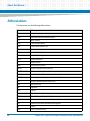
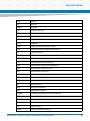
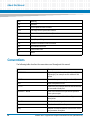
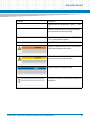
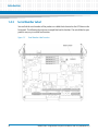
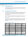
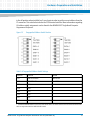
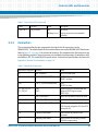
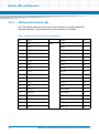
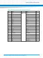
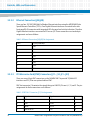
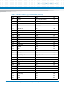
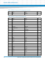
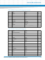
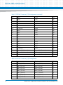
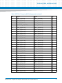
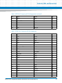
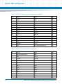
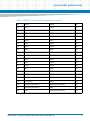
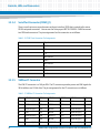
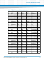
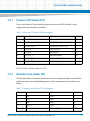
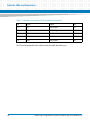
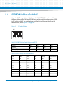
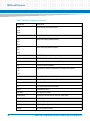
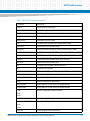
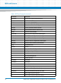
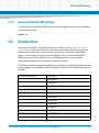
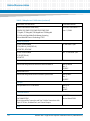
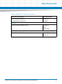
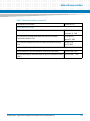
Controls, LEDs, and Connectors Table 3-11 PMC Slot 2 Connector (J23) Pin Assignments (continued) Pin Signal Signal Pin 23 AD55 AD54 24 25 AD53 GND 26 27 GND AD52 28 29 AD51 AD50 30 31 AD49 GND 32 33 GND AD48 34 35 AD47 AD46 36 37 AD45 GND 38 39 +3.3V (VIO) AD44 40 41 AD43 AD42 42 43 AD41 GND 44 45 GND AD40 46 47 AD39 AD38 48 49 AD37 GND 50 51 GND AD36 52 53 AD35 AD34 54 55 AD33 GND 56 57 +3.3V (VIO) AD32 58 59 Reserved (No Connect) Reserved (No Connect) 60 61 Reserved (No Connect) GND 62 63 GND Reserved (No Connect) 64 MVME4100ET Single Board Computer Installation and Use (6806800K76F) 61 Controls, LEDs, and Connectors 3.3.3.4 Serial Port Connector (COM1/J1) There is one front access asynchronous serial port interface (SP0) that is routed to the micro DB-9 front-panel connector. You can use the Artesyn part MTCA-CONSOLE-CABLE to convert to a DB9 male connector. The pin assignments for this connector are as follows: Table 3-12 COM1 Port Connector Pin Assignments 3.3.3.5 Pin Signal 1 No Connect 2 RX 3 TX 4 No Connect 5 GND 6 No Connect 7 RTS 8 CTS 9 No Connect VMEbus P1 Connector The VME P1 connector is a 160-pin DIN. The P1 connector provides power and VME signals for 24-bit address and 16-bit data. The pin assignments for the P1 connector are as follows: Table 3-13 VMEbus P1 Connector Pin Assignments 62 Pin ROW Z ROW A ROW B ROW C ROW D Pin 1 Reserved (N/C) D00 BBSY* D08 +5V 1 2 GND D01 BCLR* D09 GND 2 3 Reserved (N/C) D02 ACFAIL* D10 Reserved (N/C) 3 4 GND D03 BG0IN* D11 Reserved (N/C) 4 5 Reserved (N/C) D04 BG0OUT* D12 Reserved (N/C) 5 6 GND D05 BG1IN* D13 Reserved (N/C) 6 7 Reserved (N/C) D06 BG1OUT* D14 Reserved (N/C) 7 MVME4100ET Single Board Computer Installation and Use (6806800K76F) Controls, LEDs, and Connectors Table 3-13 VMEbus P1 Connector Pin Assignments (continued) Pin ROW Z ROW A ROW B ROW C ROW D Pin 8 GND D07 BG2IN* D15 Reserved (N/C) 8 9 Reserved (N/C) GND BG2OUT* GND GAP_L 9 10 GND SYSCLK BG3IN* SYSFAIL* GA0_L 10 11 Reserved (N/C) GND BG3OUT* BERR* GA1_L 11 12 GND DS1* BR0* SYSRESET* +3.3V (Not Used) 12 13 Reserved (N/C) DS0* BR1* LWORD* GA2_L 13 14 GND WRITE* BR2* AM5 +3.3V (Not Used) 14 15 Reserved (N/C) GND BR3* A23 GA3_L 15 16 GND DTACK* AM0 A22 +3.3V (Not Used) 16 17 Reserved (N/C) GND AM1 A21 GA4_L 17 18 GND AS* AM2 A20 +3.3V (Not Used) 18 19 Reserved (N/C) GND AM3 A19 Reserved (N/C) 19 20 GND IACK* GND A18 +3.3V (Not Used) 20 21 Reserved (N/C) IACKIN* SERA (N/C) A17 Reserved (N/C) 21 22 GND IACKOUT* SERB (N/C) A16 +3.3V (Not Used) 22 23 Reserved (N/C) AM4 GND A15 Reserved (N/C) 23 24 GND A07 IRQ7* A14 +3.3V (Not Used) 24 25 Reserved (N/C) A06 IRQ6* A13 Reserved (N/C) 25 26 GND A05 IRQ5* A12 +3.3V (Not Used) 26 27 Reserved (N/C) A04 IRQ4* A11 Reserved (N/C) 27 28 GND A03 IRQ3* A10 +3.3V (Not Used) 28 29 Reserved (N/C) A02 IRQ2* A09 Reserved (N/C) 29 30 GND A01 IRQ1* A08 +3.3V (Not Used) 30 31 Reserved (N/C) -12V +5VSTDBY (N/C) +12V GND 31 32 GND +5V +5V +5V +5V 32 MVME4100ET Single Board Computer Installation and Use (6806800K76F) 63 Controls, LEDs, and Connectors 3.3.3.6 VMEbus P2 Connector The VME P2 connector is a 160-pin DIN. Row B of the P2 connector provides power to the MVME4100ET and to the upper eight VMEbus address lines and additional 16 VMEbus data lines. The Z, A, C, and D pin assignments for the P2 connector are the same for both the MVME4100ET and MVME721ET, and are as follows: Table 3-14 VME P2 Connector Pinouts 64 Pin P2-Z P2-A P2-B P2-C P2-D 1 SP1RX PMC1_IO2 +5V PMC1_IO1 E1-1+ 2 GND PMC1_IO4 GND PMC1_IO3 E1-1- 3 SPITX PMC1_IO6 VRETRY_L PMC1_IO5 GND 4 GND PMC1_IO8 VA24 PMC1_IO7 E1-2+ 5 SP1CTS PMC1_IO10 VA25 PMC1_IO9 E1-2- 6 GND PMC1_IO12 VA26 PMC1_IO11 GND 7 SP1RTS PMC1_IO14 VA27 PMC1_IO13 E1-3+ 8 GND PMC1_IO16 VA28 PMC1_IO15 E1-3- 9 SP2RX PMC1_IO18 VA29 PMC1_IO17 GND 10 GND PMC1_IO20 VA30 PMC1_IO19 E1-4+ 11 SP2TX PMC1_IO22 VA31 PMC1_IO21 E1-4- 12 GND PMC1_IO24 GND PMC1_IO23 GND 13 SP2CTS PMC1_IO26 +5V PMC1_IO25 I2C_SDA 14 GND PMC1_IO28 VD16 PMC1_IO27 I2C_SCL 15 SP2RTS PMC1_IO30 VD17 PMC1_IO29 E1_LINK 16 GND PMC1_IO32 VD18 PMC1_IO31 E1_ACT 17 SP3RX PMC1_IO34 VD19 PMC1_IO33 E2_LINK 18 GND PMC1_IO36 VD20 PMC1_IO35 E2_ACT 19 SP3TX PMC1_IO38 VD21 PMC1_IO37 GND 20 GND PMC1_IO40 VD22 PMC1_IO39 E2-4- 21 SP3CTS PMC1_IO42 VD23 PMC1_IO41 E2-4+ 22 GND PMC1_IO44 GND PMC1_IO43 GND MVME4100ET Single Board Computer Installation and Use (6806800K76F) Controls, LEDs, and Connectors Table 3-14 VME P2 Connector Pinouts (continued) 3.3.3.7 Pin P2-Z P2-A P2-B P2-C P2-D 23 SP3RTS PMC1_IO46 VD24 PMC1_IO45 E2-3- 24 GND PMC1_IO48 VD25 PMC1_IO47 E2-3+ 25 SP4RX PMC1_IO50 VD26 PMC1_IO49 GND 26 GND PMC1_IO52 VD27 PMC1_IO51 E2-2- 27 SP4TX PMC1_IO54 VD28 PMC1_IO53 E2-2+ 28 GND PMC1_IO56 VD29 PMC1_IO55 GND 29 SP4CTS PMC1_IO58 VD30 PMC1_IO57 E2-1- 30 GND PMC1_IO60 VD31 PMC1_IO59 E2-1+ 31 SP4RTS PMC1_IO62 GND PMC1_IO61 GND 32 GND PMC1_IO64 +5V PMC1_IO63 +5V MVME721ET PMC I/O Module (PIM) Connectors (J10, J14) PMC Host I/O connector J10 routes only power and ground from VME P2. There are no Host I/O signals on this connector. The MVME4100ET routes PMC I/O from J14 of PMC Slot 1 to VME P2 rows A and C. The MVME721ET routes these signals (pin-for-pin) from VME P2 to PMC I/O Module connector J14. See Table 3-15 for the pin assignments. Table 3-15 MVME721 Host I/O Connector (J10) Pin Assignments Pin Signal Signal Pin 1 No Connect No Connect 2 3 No Connect No Connect 4 5 +5V No Connect 6 7 No Connect No Connect 8 9 No Connect +3.3V 10 11 No Connect No Connect 12 13 GND No Connect 14 15 No Connect No Connect 16 17 No Connect GND 18 MVME4100ET Single Board Computer Installation and Use (6806800K76F) 65 Controls, LEDs, and Connectors Table 3-15 MVME721 Host I/O Connector (J10) Pin Assignments (continued) 3.4 Pin Signal Signal Pin 19 No Connect No Connect 20 21 +5V No Connect 22 23 No Connect No Connect 24 25 No Connect +3.3V 26 27 No Connect No Connect 28 29 GND No Connect 30 31 No Connect No Connect 32 33 No Connect GND 34 35 No Connect No Connect 36 37 +5V No Connect 38 39 No Connect No Connect 40 41 No Connect +3.3V 42 43 No Connect No Connect 44 45 GND No Connect 46 47 No Connect No Connect 48 49 No Connect GND 50 51 No Connect No Connect 52 53 +5V No Connect 54 55 No Connect No Connect 56 57 No Connect +3.3V 58 59 No Connect No Connect 60 61 No Connect No Connect 62 63 No Connect No Connect 64 Headers This section describes the pin assignments of the Headers on the MVME4100ET. 66 MVME4100ET Single Board Computer Installation and Use (6806800K76F) Controls, LEDs, and Connectors 3.4.1 Processor COP Header (P4) There is one standard 16-pin header that provides access to the COP function. The pin assignments for this header are as follows: Table 3-16 Processor COP Header (P4) Pin Assignments Pin Signal Signal Pin 1 CPU_TDO No Connect 2 3 CPU_TDI CPU_TRST_L 4 5 Pull-up to +3.3V Pull-up to CPU_VIO (+3.3V) 6 7 CPU_TCK CPU_CKSTPI_L 8 9 CPU_TMS No Connect 10 11 CPU_SRST_L GND (No Connect) 12 13 CPU_HRST_L KEY (no pin) 14 15 CPU_CKSTPO_L GND 16 Pin 6 +3.3 V has a 100 W resistor to +3.3 V. 3.4.2 Boundary Scan Header (P5) The 20-pin boundary scan header provides an interface for programming the on-board PLDs and for boundary scan testing/debug purposes. The pin assignments for this header are as follows: Table 3-17 Boundary Scan Header (P5) Pin Assignments Pin Signal Signal Pin 1 TCK GND 2 3 TDO GND 4 5 TMS GND 6 7 TRST_N GND 8 9 TDI (BSCANEN_N) 10 MVME4100ET Single Board Computer Installation and Use (6806800K76F) 67 Controls, LEDs, and Connectors Table 3-17 Boundary Scan Header (P5) Pin Assignments (continued) Pin Signal Signal Pin 11 KEY No Connect 12 13 GND AUTOWR_N 14 15 GND No Connect 16 17 GND No Connect 18 19 GND No Connect 20 Pin 10 must be grounded in the cable in order to enable boundary scan. 68 MVME4100ET Single Board Computer Installation and Use (6806800K76F) Chapter 4 Functional Description 4.1 Overview The MVME4100ET VMEbus board is based on the MPC8548E System on Chip (SoC) processors. The MVME4100ET provides front panel access to one serial port with a mini DB-9 connector and two 10/100/1000 Ethernet ports with two RJ-45 connectors. The front panel includes a fail indicator LED, user-defined indicator LED, and a reset/abort switch. The MVME721ET transition module provides rear panel access to four serial ports with one RJ-45 connector per port and two 10/100/1000 Ethernet ports with two RJ-45 connectors. The transition module also provides two planar connectors for one PIM with front I/O. The block diagram for the MVME4100ET Single Board Computer is shown in Figure 4-1 and the block diagram for the MVME721ET transition module is shown in Figure 5-2. MVME4100ET Single Board Computer Installation and Use (6806800K76F) 69 Functional Description 4.2 Block Diagram The following figure is a block diagram of the MVME4100ET architecture. Figure 4-1 70 Block Diagram MVME4100ET Single Board Computer Installation and Use (6806800K76F) Functional Description 4.3 Processor The MVME4100ET is designed to support the MPC8548E processor. The processor is configured to operate at 1.3 GHz core frequency with a corresponding 533 Mb DDR2 memory bus. The MVME4100ET supports the power-on reset (POR) pin sampling method for processor reset configuration. The states of the various configuration pins on the processor are sampled when reset is de-asserted to determine the desired operating modes. Combinations of pull-up and pull-down resistors are used to set the options. Some options are fixed and some are selectable at build time by installing the proper pull-up/pull-down resistor. Refer to the MPC8548E reference manual, listed in Appendix B, Related Documentation, Manufacturers’ Documents on page 115 for additional details and/or programming information. 4.4 I2C Serial Interface and Devices The MVME4100ET provides the following on-board I2C serial devices connected to the MPC8548E I2C controller 0 interface: 8 KB serial EEPROM for VPD Two 64 KB serial EEPROMs for user configuration data storage One 256 byte serial EEPROM on SO-CDIMM for SPD Maxim DS1375 Real Time Clock On-Semi ADT7146 temperature sensor 8 KB serial EEPROM on RTM VPD The RTC implemented on the MVME4100ET provides an alarm interrupt routed to the MPC8548E PIC through the control PLD. A DS32KHz temperature controlled crystal oscillator provides the RTC clock reference. A battery backup circuit for the RTC is provided on-board. The On-Semi digital temperature sensor measures the temperature of the board and also connects to the temperature diode on the MPC8548E. The temperature sensor also provides an alarm interrupt routed to the MPC8548E PIC through the control PLD. MVME4100ET Single Board Computer Installation and Use (6806800K76F) 71 Functional Description The I2C interface is routed to the P2 connector for access to the serial EEPROM located on the transition module. The device address for the transition module serial EEPROM is user selectable using the configuration switches. Refer to Chapter 5, Transition Module for information on the switches. For programming information, see the MVME4100ET Single Board Computer Programmer’s Reference. 4.5 System Memory The MVME4100ET includes one SO-CDIMM socket. The SO-CDIMM socket supports 2 GByte DDR2 SDRAM module. The MVME4100ET supports memory speeds up to DDR533. 4.6 Timers Timing functions for the MVME4100ET are provided by four global high-resolution timers integrated into the MPC8548E plus four additional independent 32-bit timers in a PLD. The four integrated 32-bit timers are clocked by the RTC input which is driven by a 1 MHz clock. Refer to the MPC8548E reference manual, listed in Appendix B, Related Documentation, Manufacturers’ Documents on page 115 for additional details and/or programming information. The clock source for the four 32-bit timers in the PLD is 25 MHz. The timer prescaler must be configured to generate a 1 MHz timer reference. For programming information, see MVME4100ET Single Board Computer Programmer’s Reference. 4.7 Ethernet Interfaces The MVME4100ET provides four 10/100/1000 Mbps full-duplex Ethernet interfaces using the MPC8548E Ethernet Controllers. Two Broadcom BCM5482S PHYs are used. The Ethernet ports on the MPC8548E are configured to operate in RGMII mode. Two Gigabit Ethernet interfaces are routed to front panel RJ-45 connectors with integrated LEDs for speed and activity indication. The other two Gigabit Ethernet interfaces are routed to P2 for rear I/O. For programming information, see MVME4100ET Single Board Computer Programmer’s Reference. 72 MVME4100ET Single Board Computer Installation and Use (6806800K76F) Functional Description 4.8 Local Bus Interface The MVME4100ET uses the MPC8548E Local Bus Controller (LBC) for access to on-board flash and I/O registers. The LBC has programmable timing modes to support devices of different access times, as well as device widths of 8, 16, and 32 bits. The MVME4100ET uses the LBC in GPCM mode to interface to two physical banks of on-board flash, an on-board Quad UART (QUART), an MRAM, and on-board 32-bit timers along with control/status registers. Access timing for each device type is programmable and depends on the device timing data found in the VPD during initialization. A hardware flash bank write protect switch is provided on the MVME4100ET to enable write protection of the NOR Flash. Regardless of the state of the software flash write protect bit in the NOR Flash Control/Status register, write protection is enabled when this switch is ON. When this switch is OFF, write protection is controlled by the state of the software flash write protect bits and can only be disabled by clearing this bit in the NOR Flash Control/Status register. Note that the F_WE_HW bit reflects the state of the switch and is only software readable whereas the F_WP_SW bit supports both read and write operations. The MVME4100ET provides a dual boot option for booting from one of two separate boot images in the boot flash bank which are referred to as boot block A and boot block B. Boot blocks A and B are each 1 MB in size and are located at the top (highest address) 2 MB of the boot flash memory space. Block A is located at the highest 1 MB block and block B is the next highest 1 MB block. A flash boot block switch is used to select between boot block A and boot block B. When the switch is OFF, the flash memory map is normal and block A is selected. When the switch is ON, block B is mapped to the highest address. The MAP_SELECT bit in the flash Control/Status register can disable the jumper and restore the memory map to the normal configuration with block A selected. 4.8.1 Flash Memory The MVME4100ET is designed to provide 128 MB of soldered-on NOR flash memory. Two Spansion +3.3 V devices are configured to operate in 16-bit mode to form a 32-bit flash bank. This flash bank is also the boot bank and is connected to LBC Chip Select 0 and 1. A second bank of NAND flash, up to 16 GB, connected to LBC Chip Select 2 is also included. The VPD flash packet(s) will determine which devices are populated and the size of the devices. Programming details can be found in the MVME4100ET Single Board Computer Programmer’s Reference manual. MVME4100ET Single Board Computer Installation and Use (6806800K76F) 73 Functional Description 4.8.2 NVRAM The MVME4100ET includes one Everspin 512 KB MRAM device connected to the MPC8548E device control bus to provide a non-volatile memory that has unlimited writes, fast access, and long term data retention without power. The MRAM is organized as 256 K by 16. Refer to the data sheet for additional information. 4.8.3 Quad UART (QUART) The MVME4100ET contains one Quad UART device connected to the MPC8548E device control bus to provide additional asynchronous serial ports. The Quad UART provides four asynchronous serial ports which are routed to the P2 connector. The TTL-level signals of RX, TX, CTS, and RTS from each port are routed through on-board RS-232 drivers and receivers to the P2 connector where the signals can be picked up by a transition module. The reference clock frequency for the QUART is 1.8432 MHz. All UART ports are capable of signaling at up to 115 Kbaud. Refer to the ST16C554D data sheet for additional details and/or programming information. 4.8.4 Control and Timers PLD The MVME4100ET Control and Timers PLD resides on the local bus. The Control and Timers PLD provides the following functions on the board: 74 Local bus address latch Chip selects for flash banks, MRAM, and Quad UART System control and status registers Four 32-bit tick timers Watch Dog Timer RTC 1 MHz reference clock MVME4100ET Single Board Computer Installation and Use (6806800K76F) Functional Description 4.9 DUART Interface The MVME4100ET provides a front access asynchronous serial port interface using Serial Port 0 from the MPC8548E DUART. The TTL-level signals SIN, SOUT, RTS, and CTS from Serial Port 0 are routed through on-board RS-232 drivers and receivers to the mini DB-9 front panel connector. 4.10 PCI-X Port The PCI-X port on the MPC8548E connects to the TSi148 VMEbus interface and one PCI-X to PCI-X bridges, PLX PCI6520. The main PCI bus can be configured for 100 MHz PCI-X or 66 MHz PCI operation. The secondary side of the first bridge connects to the two PMC sites and is configured dynamically, with onboard logic, to operate in 33/66 MHz PCI or 66/100 MHz PCI-X mode depending on the PMCs installed. 4.10.1 Tsi148 VME Controller The VMEbus interface for the MVME4100ET is provided by the Tsi148 VMEbus controller. The Tsi148 provides the required VME, VME extensions, and 2eSST functions. TI SN74VMEH22501 transceivers are used to buffer the VME signals between the Tsi148 and the VME backplane. Refer to the Tsi148 user's manual for additional details and/or programming information. 4.11 XMC Expansion The MVME4100ET provides an additional XMC/PMC module capability through the use of a 78-pin stacking connector. This connector is connected to the PCI Express port on the processor. Up to four additional XMC/PMC modules may be added by using two expansion boards. Refer to the XMCspan manual for additional details and/or programming information. 4.12 Power Supplies The MVME4100ET on-board voltages are generated using Linear Tech LTC3828 dual output two phase controllers and LTC3416 single output controllers. The following sections detail the MVME4100ET power requirements. MVME4100ET Single Board Computer Installation and Use (6806800K76F) 75 Functional Description 4.12.1 Power Sequencing In order to meet the power sequencing requirements of the various components on the MVME4100ET, the power supply controllers implement voltage tracking which allows the power supply outputs to track each other coincidentally during power up and power down. The +3.3 V supply output is used as the tracking reference. All supply outputs will reach their final values within 20 milliseconds during power up. 4.12.2 Power Supply Monitor Logic is provided on-board to monitor the PGOOD signal from the LTC3828 and LTC3416 regulators to determine if the power supply outputs are within tolerance. If any of the power supplies fail, this logic shuts off the power supplies to avoid any component damage. If the +5.0 V power supply is still good during a fail condition, a planar red LED (PWR FAIL D9) is illuminated to indicate the power supply fail condition. 4.12.3 Power Supply Filtering and Fusing Each of the switching power supply inputs on the MVME4100ET will have an inductor to reduce switching noise from being fed back onto the +5.0 V input. The LTC3828 supplies will each have a 10 A fuse to protect the supplies from over-current in case of component failure. 4.13 Clock Distribution The clock function generates and distributes all of the clocks required for system operation. The PCI-E clocks are generated using an eight output differential clock driver. The PCI/PCI-X bus clocks are generated by the bridge chips from the PCI-E clock. Additional clocks required by individual devices are generated near the devices using individual oscillators. For clock assignments, refer to the MVME4100ET Single Board Computer Programmer’s Reference manual. 76 MVME4100ET Single Board Computer Installation and Use (6806800K76F) Functional Description 4.13.1 System Clock The system clock is driven by an oscillator. The following table defines the clock frequencies. Table 4-1 Clock Frequencies SYSCLK Core MPX (Platform) DDR2 66.67 MHz 1.3 GHz 533 MHz 266 MHz 4.13.2 Real Time Clock Input The RTC clock input is driven by a 1 MHz clock generated by the Control and Timers PLD. This provides a fixed clock reference for the MPC8548E PIC timers which software can use as a known timing reference. 4.13.3 Local Bus Controller Clock Divisor The Local Bus Controller (LBC) clock output is connected to the PLD but is not used by the internal logic. 4.14 Reset Control Logic There are multiple sources of reset on the MVME4100ET. The following sources generate a board level reset: Power-up Reset switch Watchdog timer System control register (BRD_RST) VMEbus reset A board level hard reset generates a reset for the entire SBC including the processor, local PCI/PCI-X buses, Ethernet PHYs, serial ports, flash devices, and PLD(s). If the MVME4100ET is configured as the VME system controller, the VMEbus and local Tsi148 reset input are also reset. MVME4100ET Single Board Computer Installation and Use (6806800K76F) 77 Functional Description 4.15 Real Time Clock Battery There is an on-board battery holder that provides easy replacement of a +3.0 V button cell lithium battery which provides back-up power to the on-board Real Time Clock. A battery switching circuit provides automatic switching between the +3.3 V and battery voltages. 4.16 Debug Support The MVME4100ET provides a boundary scan header for boundary scan test access and device programming. The MVME4100ET also provides a separate standard COP header for processor COP emulation. A signal from the boundary scan header controls a set of buffers that isolate the MPC8548E onto a single device chain separate from the Boundary Scan chain containing all of the scannable devices. This is a requirement of some COP debuggers to allow emulator support for the MPC8548E. 78 MVME4100ET Single Board Computer Installation and Use (6806800K76F) Chapter 5 Transition Module 5.1 Overview This chapter provides information on the features of MVME721ET transition module. It also includes a drawing of the module showing the components and rear panel connectors. MVME4100ET Single Board Computer Installation and Use (6806800K76F) 79 Transition Module 5.2 Transition Module Layout The following illustration shows the component layout and connectors on the MVME721ET transition module. Figure 5-1 Component Layout J1 J2 T2 T1 C1 U1 L1 C25 C38 L2 C39 U4 J10 S1 SMT Switch C38 S1 U2 P2 J14 80 MVME4100ET Single Board Computer Installation and Use (6806800K76F) Transition Module 5.3 Features The MVME721ET transition module is for I/O routing through the rear of a compact VMEbus chassis. It connects directly to the VME backplane in chassis’ with an 80 mm deep rear transition area. The MVME721ET is designed for use with the host MVME4100ET board. It has the following features: Table 5-1 Transition Module Features Function I/O Features One five-row P2 backplane connector for serial and Ethernet I/O passed from the SBC Four RJ-45 connectors for rear panel I/O: four asynchronous serial channels Two RJ-45 connectors with integrated LEDs for rear panel I/O: two 10/100/1000 Ethernet channels One PIM site with rear panel I/O Figure 5-2 Block Diagram MVME4100ET Single Board Computer Installation and Use (6806800K76F) 81 Transition Module 5.4 SEEPROM Address Switch, S1 A 4-position SMT configuration switch is located on the MVME721ET transition module to set the device address of the RTM serial EEPROM device and to control its write protection (if SW4 is OFF, write is enabled). The switch settings are defined in the following table. To see the switch location, refer to Figure 5-1 on page 80. Figure 5-3 S1 Switch Positions ON 1 2 3 4 Table 5-2 SEEPROM Address Switch Assignments (RTM) Position SW4 SW3 SW2 SW1 Function WP A(2) A(1) A(0) Default (OFF) 0 1 1 1 Table 5-3 Switch Settings and Device Addresses 82 SW4 SW3 SW2 SW1 A(2:0) Device Address OFF ON ON ON 000 $A0 OFF ON ON OFF 001 $A2 OFF ON OFF ON 010 $A4 OFF ON OFF OFF 011 $A6 OFF OFF ON ON 100 $A8 OFF OFF ON OFF 101 $AA (default) OFF OFF OFF ON 110 $AC OFF OFF OFF OFF 111 $AE MVME4100ET Single Board Computer Installation and Use (6806800K76F) Transition Module 5.5 Rear Panel Connectors The MVME721ET transition module provides the following connectors. All connectors use standard pin assignments in compliance with the VMEbus specifications. Table 5-4 Transition Module Connectors Connector Function J1A, J1B, J1C, J1D COM port connectors J2A 10/100/1000Mb/s Ethernet connector J2B 10/100/1000Mb/s Ethernet connector J10 PIM power/ground J14 PIM I/O P2 VME backplane connector MVME4100ET Single Board Computer Installation and Use (6806800K76F) 83 Transition Module PMC I/O (PIM) connector J10 routes only power and ground from VME P2 connector. There are no host I/O signals on this connector. The MVME4100ET routes PMC I/O from J14 of PMC Slot 1 to VME P2 rows A and C. The MVME721ET routes these signals (pin-for-pin) from VME P2 to PMC I/O module connector J14. Figure 5-4 Rear Panel Connectors and LEDs COM2 COM3 COM4 COM5 ACT SPEED ACT SPEED G Enet 1 G Enet 2 PMC Site 84 MVME4100ET Single Board Computer Installation and Use (6806800K76F) Transition Module There are two sets of ACT and SPEED LEDs, one set for each Ethernet connector. They are described in the following table. Table 5-5 Transition Module LEDs 5.6 LED Function ACT Activity for Ethernet or Gigabit Ethernet connector SPEED 10/100/1000Mb/s of Ethernet connectors PMC Input/Output Module If a PMC Input/output Module (PIM) has already been installed on the MVME721ET, or you are installing a transition module as it has been shipped from the factory, disregard this procedure and refer to Transition Module on page 36. Procedure For PIM installation, perform the following steps: 1. Attach an ESD strap to your wrist. 2. Attach the other end of the ESD strap to the chassis as a ground. The ESD strap must be secured to your wrist and to ground throughout the procedure. 3. Carefully remove the transition module from its packaging and lay it flat on a stable surface. 4. Remove the PIM filler from the front panel of the transition module. 5. Slide the face plate (front bezel) of the PIM module into the front panel opening from behind and place the PIM module on top of the transition module, aligned with the appropriate two PIM connectors. The two connectors on the underside of the PIM module should then connect smoothly with the corresponding connectors on the transition module (J10 and J14). MVME4100ET Single Board Computer Installation and Use (6806800K76F) 85 Transition Module 6. Insert the four short Phillips screws, provided with the PIM, through the holes on the bottom side of the transition module into the PIM front bezel and rear standoffs. Tighten the screws. Refer to the following figure for proper screw/board alignment. The example below may not accurately represent your MVME721ET. Figure 5-5 Installing the PIM PIM Alignment 86 MVME4100ET Single Board Computer Installation and Use (6806800K76F) Chapter 6 MOTLoad Firmware 6.1 Overview The MOTLoad firmware package serves as a board power-up and initialization package, as well as a vehicle from which user applications can be booted. A secondary function of the MOTLoad firmware is to serve in some respects as a test suite providing individual tests for certain devices. This chapter includes a list of standard MOTLoad commands, the default VME and firmware settings that are changeable by the user, remote start, and the alternate boot procedure. MOTLoad is controlled through an easy-to-use, UNIX-like, command line interface. The MOTLoad software package is similar to many end-user applications designed for the embedded market, such as the real time operating systems currently available. Refer to the MOTLoad Firmware Package User’s Manual, listed in Appendix B, Related Documentation, for more details. 6.2 Implementation and Memory Requirements The implementation of MOTLoad and its memory requirements are product specific. The MVME4100ET single-board computer (SBC) is offered with a range of memory (for example, DRAM or flash). Typically, the smallest amount of on-board DRAM that an SBC has is 32 MB. Each supported product line has its own unique MOTLoad binary image(s). Currently the largest MOTLoad compressed image is less than 1 MB in size. 6.3 MOTLoad Commands MOTLoad supports two types of commands (applications): utilities and tests. Both types of commands are invoked from the MOTLoad command line in a similar fashion. Beyond that, MOTLoad utilities and MOTLoad tests are distinctly different. 6.3.1 Utilities The definition of a MOTLoad utility application is very broad. Simply stated, it is considered a MOTLoad command if it is not a MOTLoad test. Typically, MOTLoad utility applications are applications that aid the user in some way (that is, they do something useful). From the perspective of MOTLoad, examples of utility applications are: configuration, data/status displays, data manipulation, help routines, data/status monitors, and so on. MVME4100ET Single Board Computer Installation and Use (6806800K76F) 87 MOTLoad Firmware Operationally, MOTLoad utility applications differ from MOTLoad test applications in several ways: 6.3.2 Only one utility application operates at any given time (that is, multiple utility applications cannot be executing concurrently). Utility applications may interact with the user. Most test applications do not. Tests A MOTLoad test application determines whether or not the hardware meets a given standard. Test applications are validation tests. Validation is conformance to a specification. Most MOTLoad tests are designed to directly validate the functionality of a specific SBC subsystem or component. It is possible for a board's component to fail in the user application but pass specification conformance. These tests validate the operation of such SBC modules as: dynamic memory, external cache, NVRAM, real time clock, and so on. All MOTLoad tests are designed to validate functionality with minimum user interaction. Once launched, most MOTLoad tests operate automatically without any user interaction. There are a few tests where the functionality being validated requires user interaction (that is, switch tests, interactive plug-in hardware modules, and so on). Most MOTLoad test results (errordata/status-data) are logged, not printed. Test results are not preserved and therefore not available to user applications subsequent to their execution. All MOTLoad tests/commands have complete and separate descriptions (refer to the MOTLoad Firmware Package User’s Manual for this information). All devices that are available to MOTLoad for validation/verification testing are represented by a unique device path string. Most MOTLoad tests require the operator to specify a test device at the MOTLoad command line when invoking the test. A listing of all device path strings can be displayed through the devShow command. If an SBC device does not have a device path string, it is not supported by MOTLoad and cannot be directly tested. There are a few exceptions to the device path string requirement, like testing RAM, which is not considered a true device and can be directly tested without a device path string. Refer to the devShow command description page in the MOTLoad Firmware Package User’s Manual. 88 MVME4100ET Single Board Computer Installation and Use (6806800K76F) MOTLoad Firmware Most MOTLoad tests can be organized to execute as a group of related tests (a testSuite) through the use of the testSuite command. The expert operator can customize their testing by defining and creating a custom testSuite(s). The list of built-in and user-defined MOTLoad testSuites, and their test contents can be obtained by entering testSuite -d at the MOTLoad prompt. All testSuites that are included as part of a product specific MOTLoad firmware package are product specific. For more information, refer to the testSuite command description page in the MOTLoad Firmware Package User’s Manual. Test results and test status are obtained through the testStatus, errorDisplay, and taskActive commands. Refer to the appropriate command description page in the MOTLoad Firmware Package User’s Manual for more information. 6.3.3 Command List The following table provides a list of all current MOTLoad commands. Products supported by MOTLoad may or may not employ the full command set. Typing help at the MOTLoad command prompt will display all commands supported by MOTLoad for a given product. Table 6-1 MOTLoad Commands Command Description as One-Line Instruction Assembler bcb Block Compare Byte/Halfword/Word bch bcw bdTempShow Display Current Board Temperature bfb Block Fill Byte/Halfword/Word bfh bfw blkCp Block Copy blkFmt Block Format blkRd Block Read blkShow Block Show Device Configuration Data blkVe Block Verify blkWr Block Write MVME4100ET Single Board Computer Installation and Use (6806800K76F) 89 MOTLoad Firmware Table 6-1 MOTLoad Commands (continued) Command Description bmb Block Move Byte/Halfword/Word bmh bmw br Assign/Delete/Display User-Program Break-Points bsb Block Search Byte/Halfword/Word bsh bsw bvb Block Verify Byte/Halfword/Word bvh bvw cdDir ISO9660 File System Directory Listing cdGet ISO9660 File System File Load clear Clear the Specified Status/History Table(s) cm Turns on Concurrent Mode csb Calculates a Checksum Specified by Command-line Options csh csw 90 devShow Display (Show) Device/Node Table diskBoot Disk Boot (Direct-Access Mass-Storage Device) downLoad Down Load S-Record from Host ds One-Line Instruction Disassembler echo Echo a Line of Text elfLoader ELF Object File Loader errorDisplay Display the Contents of the Test Error Status Table eval Evaluate Expression execProgram Execute Program fatDir FAT File System Directory Listing fatGet FAT File System File Load MVME4100ET Single Board Computer Installation and Use (6806800K76F) MOTLoad Firmware Table 6-1 MOTLoad Commands (continued) Command Description fdShow Display (Show) File Discriptor flashLock Flash Memory Sector Lock flashProgram Flash Memory Program flashShow Display Flash Memory Device Configuration Data flashUnlock Flash Memory Sector Unlock gd Go Execute User-Program Direct (Ignore Break-Points) gevDelete Global Environment Variable Delete gevDump Global Environment Variable(s) Dump (NVRAM Header + Data) gevEdit Global Environment Variable Edit gevInit Global Environment Variable Area Initialize (NVRAM Header) gevList Global Environment Variable Labels (Names) Listing gevShow Global Environment Variable Show gn Go Execute User-Program to Next Instruction go Go Execute User-Program gt Go Execute User-Program to Temporary Break-Point hbd Display History Buffer hbx Execute History Buffer Entry help Display Command/Test Help Strings l2CacheShow Display state of L2 Cache and L2CR register contents l3CacheShow Display state of L3 Cache and L3CR register contents mdb Memory Display Bytes/Halfwords/Words mdh mdw memShow Display Memory Allocation mmb Memory Modify Bytes/Halfwords/Words mmh mmw mpuFork Execute program from idle processor MVME4100ET Single Board Computer Installation and Use (6806800K76F) 91 MOTLoad Firmware Table 6-1 MOTLoad Commands (continued) 92 Command Description mpuShow Display multi-processor control structure mpuStart Start the other MPU netBoot Network Boot (BOOT/TFTP) netShow Display Network Interface Configuration Data netShut Disable (Shutdown) Network Interface netStats Display Network Interface Statistics Data noCm Turns off Concurrent Mode pciDataRd Read PCI Device Configuration Header Register pciDataWr Write PCI Device Configuration Header Register pciDump Dump PCI Device Configuration Header Register pciShow Display PCI Device Configuration Header Register pciSpace Display PCI Device Address Space Allocation ping Ping Network Host portSet Port Set portShow Display Port Device Configuration Data rd User Program Register Display reset Reset System rs User Program Register Set set Set Date and Time sromRead SROM Read sromWrite SROM Write sta Symbol Table Attach stl Symbol Table Lookup stop Stop Date and Time (Power-Save Mode) taskActive Display the Contents of the Active Task Table tc Trace (Single-Step) User Program td Trace (Single-Step) User Program to Address MVME4100ET Single Board Computer Installation and Use (6806800K76F) MOTLoad Firmware Table 6-1 MOTLoad Commands (continued) Command Description testDisk Test Disk testEnetPtP Ethernet Point-to-Point testNvramRd NVRAM Read testNvramRdWr NVRAM Read/Write (Destructive) testRam RAM Test (Directory) testRamAddr RAM Addressing testRamAlt RAM Alternating testRamBitToggle RAM Bit Toggle testRamBounce RAM Bounce testRamCodeCopy RAM Code Copy and Execute testRamEccMonitor Monitor for ECC Errors testRamMarch RAM March testRamPatterns RAM Patterns testRamPerm RAM Permutations testRamQuick RAM Quick testRamRandom RAM Random Data Patterns testRtcAlarm RTC Alarm testRtcReset RTC Reset testRtcRollOver RTC Rollover testRtcTick RTC Tick testSerialExtLoop Serial External Loopback testSeriallntLoop Serial Internal Loopback testStatus Display the Contents of the Test Status Table testSuite Execute Test Suite testSuiteMake Make (Create) Test Suite testWatchdogTimer Tests the Accuracy of the Watchdog Timer Device tftpGet TFTP Get MVME4100ET Single Board Computer Installation and Use (6806800K76F) 93 MOTLoad Firmware Table 6-1 MOTLoad Commands (continued) 6.4 Command Description tftpPut TFTP Put time Display Date and Time transparentMode Transparent Mode (Connect to Host) tsShow Display Task Status upLoad Up Load Binary Data from Target version Display Version String(s) vmeCfg Manages user specified VME configuration parameters vpdDisplay VPD Display vpdEdit VPD Edit wait Wait for Test Completion waitProbe Wait for I/O Probe to Complete Using the Command Line Interface Interaction with MOTLoad is performed via a command line interface through a serial port on the single board computer, which is connected to a terminal or terminal emulator (for example, Window’s Hypercomm). The default MOTLoad serial port settings are: 9600 baud, 8 bits, no parity. The MOTLoad command line interface is similar to a UNIX command line shell interface. Commands are initiated by entering a valid MOTLoad command (a text string) at the MOTLoad command line prompt and pressing the carriage-return key to signify the end of input. MOTLoad then performs the specified action. An example of a MOTLoad command line prompt is shown below. The MOTLoad prompt changes according to what product it is used on (for example, MVME6100, MVME3100, MVME4100ET). Example: MVME4100> If an invalid MOTLoad command is entered at the MOTLoad command line prompt, MOTLoad displays a message that the command was not found. 94 MVME4100ET Single Board Computer Installation and Use (6806800K76F) MOTLoad Firmware Example: MVME4100> mytest "mytest" not found MVME4100> If the user enters a partial MOTLoad command string that can be resolved to a unique valid MOTLoad command and presses the carriage-return key, the command is executed as if the entire command string had been entered. This feature is a user-input shortcut that minimizes the required amount of command line input. MOTLoad is an ever changing firmware package, so user-input shortcuts may change as command additions are made. Example: MVME4100>[ver]sion Copyright: Motorola Inc.1999-2005, All Rights Reserved MOTLoad RTOS Version 2.0, PAL Version 1.0 RM01 Mon Aug 29 15:24:13 MST 2005 MVME4100> Example: MVME4100> ver Copyright: Motorola Inc.1999-2005, All Rights Reserved MOTLoad RTOS Version 2.0, PAL Version 1.0 RM01 Mon Aug 29 15:24:13 MST 2005 MVME4100> If the partial command string cannot be resolved to a single unique command, MOTLoad informs the user that the command was ambiguous. Example: MVME4100> te "te" ambiguous MVME4100> MVME4100ET Single Board Computer Installation and Use (6806800K76F) 95 MOTLoad Firmware 6.4.1 Rules There are a few things to remember when entering a MOTLoad command: Multiple commands are permitted on a single command line, provided they are separated by a single semicolon (;). Spaces separate the various fields on the command line (command/arguments/options). The argument/option identifier character is always preceded by a hyphen (-) character. Options are identified by a single character. Option arguments immediately follow (no spaces) the option. All commands, command options, and device tree strings are case sensitive. Example: MVME4100> flashProgram –d/dev/flash0 –n00100000 For more information on MOTLoad operation and function, refer to the MOTLoad Firmware Package User’s Manual. 6.4.2 Help Each MOTLoad firmware package has an extensive, product-specific help facility that can be accessed through the help command. The user can enter help at the MOTLoad command line to display a complete listing of all available tests and utilities. Example MVME4100> help For help with a specific test or utility the user can enter the following at the MOTLoad prompt: help <command_name> The help command also supports a limited form of pattern matching. Refer to the help command page. Example MVME4100> help testRam 96 MVME4100ET Single Board Computer Installation and Use (6806800K76F) MOTLoad Firmware Usage: testRam [-aPh] [-bPh] [-iPd] [-nPh] [-tPd] [-v] Description: RAM Test [Directory] Argument/Option Description -a Ph: Address to Start (Default = Dynamic Allocation) -b Ph: Block Size (Default = 16KB) -i Pd: Iterations (Default = 1) -n Ph: Number of Bytes (Default = 1MB) -t Ph: Time Delay Between Blocks in OS Ticks (Default = 1) -v O : Verbose Output MVME4100> 6.5 Firmware Settings The following sections provide additional information pertaining to the MVME4100ET VME bus interface settings as configured by MOTLoad. A few VME settings are controlled by hardware jumpers while the majority of the VME settings are managed by the firmware command utility vmeCfg. VME settings in MOTLoad are preserved through the use of Global Environment Variables (GEVs). Configuration GEVs are executed only at power-on reset. Therefore, if VME configuration changes are implemented through vmeCfg, a board reset must be effected for the changes to be implemented in MOTLoad. 6.5.1 Default VME Settings As shipped from the factory, the MVME4100ET has the following VME configuration programmed via Global Environment Variables (GEVs) for the Tsi148 VME controller. The firmware allows certain VME settings to be changed in order for the user to customize the environment. The following is a description of the default VME settings that are changeable by the user. For more information, refer to the MOTLoad User’s Manual and Tundra’s Tsi148 User Manual, listed in Appendix B, Related Documentation. MVME4100> vmeCfg -s -m Displaying the selected Default VME Setting - interpreted as follows: VME PCI Master Enable [Y/N] = Y MVME4100> MVME4100ET Single Board Computer Installation and Use (6806800K76F) 97 MOTLoad Firmware The PCI Master is enabled. MVME4100> vmeCfg -s -r234 Displaying the selected Default VME Setting - interpreted as follows: VMEbus Master Control Register = 00000003 MVME4100> The VMEbus Master Control Register is set to the default (RESET) condition. MVME4100> vmeCfg -s -r238 Displaying the selected Default VME Setting - interpreted as follows: VMEbus Control Register = 00000008 MVME4100> The VMEbus Control Register is set to a Global Timeout of 2048 seconds. MVME4100> vmeCfg -s -r414 Displaying the selected Default VME Setting - interpreted as follows: CRG Attribute Register = 00000000 CRG Base Address Upper Register = 00000000 CRG Base Address Lower Register = 00000000 MVME4100> The CRG Attribute Register is set to the default (RESET) condition. MVME4100> vmeCfg –s –i0 Displaying the selected Default VME Setting - interpreted as follows: Inbound Image 0 Attribute Register = 000227AF Inbound Image 0 Starting Address Upper Register = 00000000 Inbound Image 0 Starting Address Lower Register = 00000000 Inbound Image 0 Ending Address Upper Register = 00000000 Inbound Image 0 Ending Address Lower Register = 1FFF0000 Inbound Image 0 Translation Offset Upper Register = 00000000 Inbound Image 0 Translation Offset Lower Register = 00000000 MVME4100> 98 MVME4100ET Single Board Computer Installation and Use (6806800K76F) MOTLoad Firmware Inbound window 0 (ITAT0) is not enabled; Virtual FIFO at 256 bytes, 2eSST timing at SST320, respond to 2eSST, 2eVME, MBLT, and BLT cycles, A32 address space, respond to Supervisor, User, Program, and Data cycles. Image maps from 0x00000000 to 0x1FFF0000 on the VMEbus, translates 1x1 to the PCI-X bus (thus 1x1 to local memory). To enable this window, set bit 31 of ITAT0 to 1. MVME4100> vmeCfg –s –o1 Displaying the selected Default VME Setting - interpreted as follows: Outbound Image 1 Attribute Register = 80001462 Outbound Image 1 Starting Address Upper Register = 00000000 Outbound Image 1 Starting Address Lower Register = 91000000 Outbound Image 1 Ending Address Upper Register = 00000000 Outbound Image 1 Ending Address Lower Register = AFFF0000 Outbound Image 1 Translation Offset Upper Register = 00000000 Outbound Image 1 Translation Offset Lower Register = 70000000 Outbound Image 1 2eSST Broadcast Select Register = 00000000 MVME4100> Outbound window 1 (OTAT1) is enabled, 2eSST timing at SST320, transfer mode of 2eSST, A32/D32 Supervisory access. The window accepts transfers on the PCI-X Local Bus from 0x91000000-0xAFFF0000 and translates them onto the VMEbus using an offset of 0x70000000, thus an access to 0x91000000 on the PCI-X Local Bus becomes an access to 0x01000000 on the VMEbus. MVME4100> vmeCfg –s –o2 Displaying the selected Default VME Setting - interpreted as follows: Outbound Image 2 Attribute Register = 80001061 Outbound Image 2 Starting Address Upper Register = 00000000 Outbound Image 2 Starting Address Lower Register = B0000000 Outbound Image 2 Ending Address Upper Register = 00000000 Outbound Image 2 Ending Address Lower Register = B0FF0000 Outbound Image 2 Translation Offset Upper Register = 00000000 Outbound Image 2 Translation Offset Lower Register = 40000000 Outbound Image 2 2eSST Broadcast Select Register = 00000000 MVME4100> MVME4100ET Single Board Computer Installation and Use (6806800K76F) 99 MOTLoad Firmware Outbound window 2 (OTAT2) is enabled, 2eSST timing at SST320, transfer mode of SCT, A24/D32 Supervisory access. The window accepts transfers on the PCI-X Local Bus from 0xB0000000-0xB0FF0000 and translates them onto the VMEbus using an offset of 0x40000000, thus an access to 0xB0000000 on the PCI-X Local Bus becomes an access to 0xF0000000 on the VMEbus. MVME4100> vmeCfg –s –o3 Displaying the selected Default VME Setting - interpreted as follows: Outbound Image 3 Attribute Register = 80001061 Outbound Image 3 Starting Address Upper Register = 00000000 Outbound Image 3 Starting Address Lower Register = B3FF0000 Outbound Image 3 Ending Address Upper Register = 00000000 Outbound Image 3 Ending Address Lower Register = B3FF0000 Outbound Image 3 Translation Offset Upper Register = 00000000 Outbound Image 3 Translation Offset Lower Register = 4C000000 Outbound Image 3 2eSST Broadcast Select Register = 00000000 MVME4100> Outbound window 3 (OTAT3) is enabled, 2eSST timing at SST320, transfer mode of SCT, A16/D32 Supervisory access. The window accepts transfers on the PCI-X Local Bus from 0xB3FF0000-0xB3FF0000 and translates them onto the VMEbus using an offset of 0x4C000000, thus an access to 0xB3FF0000 on the PCI-X Local Bus becomes an access to 0xFFFF0000 on the VMEbus. MVME4100> vmeCfg –s –o7 Displaying the selected Default VME Setting - interpreted as follows: Outbound Image 7 Attribute Register = 80001065 Outbound Image 7 Starting Address Upper Register Outbound Image 7 Starting Address Lower Register Outbound Image 7 Ending Address Upper Register = Outbound Image 7 Ending Address Lower Register = 100 = 00000000 = B1000000 00000000 B1FF0000 MVME4100ET Single Board Computer Installation and Use (6806800K76F) MOTLoad Firmware Outbound Image 7 Translation Offset Upper Register = 00000000 Outbound Image 7 Translation Offset Lower Register = 4F000000 Outbound Image 7 2eSST Broadcast Select Register = 00000000 MVME4100> Outbound window 7 (OTAT7) is enabled, 2eSST timing at SST320, transfer mode of SCT, CR/CSR Supervisory access. The window accepts transfers on the PCI-X Local Bus from 0xB1000000-0xB1FF0000 and translates them onto the VMEbus using an offset of 0x4F000000, thus an access to 0xB1000000 on the PCI-X Local Bus becomes an access to 0x00000000 on the VMEbus. 6.5.2 Control Register/Control Status Register Settings The CR/CSR base address is initialized to the appropriate setting based on the Geographical address; that is, the VME slot number. See the VME64 Specification and the VME64 Extensions for details. As a result, a 512 KB CR/CSR area can be accessed from the VMEbus using the CR/CSR AM code. 6.5.3 Displaying VME Settings To display the changeable VME setting, type the following at the firmware prompt: To display Master Enable state: vmeCfg –s –m To display selected Inbound Window state: vmeCfg –s –i(0 - 7) To display selected Outbound Window state: vmeCfg –s –o(0 - 7) To display Master Control Register state: vmeCfg –s –r234 To display Miscellaneous Control Register state: vmeCfg –s –r238 To display CRG Attribute Register state: vmeCfg –s –r414 MVME4100ET Single Board Computer Installation and Use (6806800K76F) 101 MOTLoad Firmware 6.5.4 Editing VME Settings To edit the changeable VME setting, type the following at the firmware prompt: 6.5.5 Edits Master Enable state: vmeCfg –e –m Edits selected Inbound Window state: vmeCfg –e –i(0 - 7) Edits selected Outbound Window state: vmeCfg –e –o(0 - 7) Edits Master Control Register state: vmeCfg –e –r234 Edits Control Register state: vmeCfg –e –r238 Edits CRG Attribute Register state: vmeCfg –e –r414 Deleting VME Settings To delete the changeable VME setting (restore default value), type the following at the firmware prompt: 102 Deletes Master Enable state: vmeCfg –d –m Deletes selected Inbound Window state: vmeCfg –d –i(0 - 7) Deletes selected Outbound Window state: vmeCfg –d –o(0 - 7) Deletes Master Control Register state: vmeCfg –d –r234 Deletes Control Register state: vmeCfg –d –r238 Deletes CRG Attribute Register state: vmeCfg –d –r414 MVME4100ET Single Board Computer Installation and Use (6806800K76F) MOTLoad Firmware 6.5.6 Restoring Default VME Settings To restore all of the changeable VME setting back to their default settings, type the following at the firmware prompt: vmeCfg –z 6.6 Remote Start As described in the MOTLoad Firmware Package User's Manual, listed in Appendix B, Related Documentation, remote start allows the user to obtain information about the target board, download code and/or data, modify memory on the target, and execute a downloaded program. These transactions occur across the VMEbus in the case of the MVME4100ET. MOTLoad uses one of four mailboxes in the Tsi148 VME controller as the inter-board communication address (IBCA) between the host and the target. CR/CSR slave addresses configured by MOTLoad are assigned according to the installation slot in the backplane, as indicated by the VME64 Specification. For reference, the following values are provided: CS/CSR Starting Address Slot Position 1 0x0008.0000 2 0x0010.0000 3 0x0018.0000 4 0x0020.0000 5 0x0028.0000 6 0x0030.0000 7 0x0038.0000 8 0x0040.0000 9 0x0048.0000 A 0x0050.0000 B 0x0058.0000 C 0x0060.0000 MVME4100ET Single Board Computer Installation and Use (6806800K76F) 103 MOTLoad Firmware For further details on CR/CSR space, refer to the VME64 Specification, listed in Appendix B, Related Documentation. The MVME4100ET uses a TSi148 for its PCI/X-to-VME bus bridge. The offsets of the mailboxes in the TSi148 are defined in the TSi148 VMEBus PCI/X-to-VME User Manual, listed in Appendix B, Related Documentation, but are listed here for reference: Mailbox 0 is at offset 7f610 in the CR/CSR space Mailbox 1 is at offset 7f614 in the CR/CSR space Mailbox 2 is at offset 7f618 in the CR/CSR space Mailbox 3 is at offset 7f61C in the CR/CSR space The selection of the mailbox used by remote start on an individual MVME4100ET is determined by the setting of a global environment variable (GEV). The default mailbox is zero. Another GEV controls whether remote start is enabled (default) or disabled. Refer to the Remote Start appendix in the MOTLoad Firmware Package User's Manual for remote start GEV definitions. The MVME4100ET’s IBCA needs to be mapped appropriately through the master’s VMEbus bridge. For example, to use remote start using mailbox 0 on an MVME4100ET installed in slot 5, the master would need a mapping to support reads and writes of address 0x002ff610 in VME CR/CSR space (0x280000 + 0x7f610). 6.7 Boot Images Valid boot images whether POST, USER, or Alternate MOTLoad, are located on 1 MB boundaries within the upper 8 MB of flash. The image may exceed 1 MB in size. An image is determined valid through the presence of two "valid image keys" and other sanity checks. A valid boot image begins with a structure as defined in the following table: 104 Name Type Size Notes UserDefined unsigned integer 8 User defined ImageKey 1 unsigned integer 1 0x414c5420 ImageKey 2 unsigned integer 1 0x424f4f54 ImageChecksum unsigned integer 1 Image checksum ImageSize unsigned integer 1 Must be a multiple of 4 ImageName unsigned character 20 User defined MVME4100ET Single Board Computer Installation and Use (6806800K76F) MOTLoad Firmware 6.7.1 Name Type Size Notes ImageRamAddress unsigned integer 1 RAM address ImageOffset unsigned integer 1 Offset from header start to entry ImageFlags unsigned integer 1 Refer to Image Flags on page 106 ImageVersion unsigned integer 1 User defined Reserved unsigned integer 8 Reserved for expansion Checksum Algorithm The checksum algorithm is a simple unsigned word add of each word (4 byte) location in the image. The image must be a multiple of 4 bytes in length (word-aligned). The content of the checksum location in the header is not part of the checksum calculation. The calculation assumes the location to be zero. The algorithm is implemented by the MOTLoad command csUserAltBoot or by using the following code: Unsigned int checksum( Unsigned int *startPtr,/* starting address */ Unsigned int endPtr/* ending address */ ) { unsigned int checksum=0; while (startPtr < endPtr) { checksum += *startPtr; startPtr++; } return(checksum); } MVME4100ET Single Board Computer Installation and Use (6806800K76F) 105 MOTLoad Firmware 6.7.2 Image Flags The image flags of the header define various bit options that control how the image will be executed. Table 6-2 MOTLoad Image Flags Name Value Interpretation COPY_TO_RAM 0x00000001 Copy image to RAM at ImageRamAddress before execution IMAGE_MCG 0x00000002 Alternate MOTLoad image IMAGE_POST 0x00000004 POST image DONT_AUTO_RUN 0x00000008 Image not to be executed COPY_TO_RAM If set, this flag indicates that the image is to be copied to RAM at the address specified in the header before control is passed. If not set, the image will be executed in flash. In both instances, control will be passed at the image offset specified in the header from the base of the image. IMAGE_MCG If set, this flag defines the image as being an Alternate MOTLoad, as opposed to USER, image. This bit should not be set by developers of alternate boot images. IMAGE_POST If set, this flag defines the image as being a power-on self-test image. This bit flag is used to indicate that the image is a diagnostic and should be run prior to running either USER or MCG boot images. POST images are expected, but not required, to return to the boot block code upon completion. DONT_AUTO_RUN If set, this flag indicates that the image is not to be selected for automatic execution. A user, through the interactive command facility, may specify the image to be executed. MOTLoad currently uses an Image Flag value of 0x3, which identifies itself as an alternate MOTLoad image that executes from RAM. MOTLoad currently does not support execution from flash. 106 MVME4100ET Single Board Computer Installation and Use (6806800K76F) MOTLoad Firmware 6.7.3 User Images These images are user-developer boot code; for example, a VxWorks bootrom image. Such images may expect the system software state to be as follows upon entry: The MMU is disabled. L1 instruction cache has been initialized and is enabled. L1 data cache has been initialized (invalidated) and is disabled. L2 cache is disabled. L3 cache is disabled. RAM has been initialized and is mapped starting at CPU address 0. If RAM ECC or parity is supported, RAM has been scrubbed of ECC or parity errors. The active flash bank (boot) is mapped from the upper end of the address space. If specified by COPY_TO_RAM, the image has been copied to RAM at the address specified by ImageRamAddress. CPU register R1 (the stack pointer) has been initialized to a value near the end of RAM. CPU register R3 is added to the following structure: typedef struct altBootData { unsigned int ramSize;/* board's RAM size in MB */ void flashPtr;/* ptr to this image in flash */ char boardType[16];/* name string, eg MVME4100 */ void globalData;/* 16K, zeroed, user defined */ unsigned int reserved[12]; } altBootData_t; 6.7.4 Alternate Boot Data Structure The globalData field of the alternate boot data structure points to an area of RAM which was initialized to zeroes by the boot loader. This area of RAM is not cleared by the boot loader after execution of a POST image or other alternate boot image is executed. It is intended to provide a user a mechanism to pass POST image results to subsequent boot images. The boot loader performs no other initialization of the board than that specified prior to the transfer of control to either a POST, USER, or Alternate MOTLoad image. Alternate boot images need to initialize the board to whatever state the image may further require for its execution. MVME4100ET Single Board Computer Installation and Use (6806800K76F) 107 MOTLoad Firmware POST images are expected, but not required, to return to the boot loader. Upon return, the boot loader proceeds with the scan for an executable alternate boot image. POST images that return control to the boot loader must ensure that upon return, the state of the board is consistent with the state that the board was in at POST entry. USER images should not return control to the boot loader. 6.7.5 Alternate Boot Images and Safe Start Some later versions of MOTLoad support alternate boot images and a safe start recovery procedure. If safe start is available on the MVME4100ET, alternate boot images are supported. With alternate boot image support, the boot loader code in the boot block examines the upper 8 MB of the flash bank for alternate boot images. If an image is found, control is passed to the image. 6.7.6 Boot Image Firmware Scan The scan is performed by examining each 1 MB boundary for a defined set of flags that identify the image as being POST, USER, or Alternate MOTLoad. POST is a user-developed Power On Self Test that would perform a set of diagnostics and then return to the boot loader image. USER would be a boot image, such as the VxWorks bootrom, which would perform board initialization. A bootable VxWorks kernel would also be a USER image. Boot images are not restricted to being 1 MB or less in size; however, they must begin on a 1 MB boundary within the 8 MB of the scanned flash bank. The flash bank structure is shown below: 108 Address Usage 0xFFF00000 to 0xFFFFFFFF Boot block. Recovery code. 0xFFE00000 to 0XFFFFFFFF Backup MOTLoad image 0xFFD00000 to 0xFFDFFFFF First possible alternate image 0xFFC00000 to 0xFFCFFFFF Second possible alternate image .... Alternate boot images 0xFF899999 to 0xFF8FFFFF Bottom of flash (flash size varies per product) MVME4100ET Single Board Computer Installation and Use (6806800K76F) MOTLoad Firmware The scan is performed downwards beginning at the location of the first possible alternate image and searches first for POST, then USER, and finally Alternate MOTLoad images. In the case of multiple images of the same type, control is passed to the first image encountered in the scan. Safe Start, whether invoked by hitting ESC on the console within the first five seconds following power-on reset or by setting the Safe Start jumper, interrupts the scan process. The user may then display the available boot images and select the desired image. The feature is provided to enable recovery in cases when the programmed Alternate Boot Image is no longer desired. The following output is an example of an interactive Safe Start: ABCDEInteractive Boot Mode Entered boot> ? Interactive boot commands: 'd':show directory of alternate boot images 'c':continue with normal startup 'q':quit without executing any alternate boot image 'r [address]':execute specified (or default) alternate image 'p [address]':execute specified (or default) POST image '?':this help screen 'h':this help screen boot> d Addr FFE00000 Size 00100000 Flags 00000003 Name: MOTLoad Addr FFD00000 Size 00100000 Flags 00000003 Name: MOTLoad boot> c NOPQRSTUVabcdefghijk#lmn3opqrsstuvxyzaWXZ Copyright Motorola Inc. 1999-2004, All Rights Reserved MOTLoad RTOS Version 2.0, PAL Version 0.b EA02 ... MVME4100> 6.8 Startup Sequence The firmware startup sequence following reset of MOTLoad is to: Initialize cache, MMU, FPU, and other CPU internal items Initialize the memory controller MVME4100ET Single Board Computer Installation and Use (6806800K76F) 109 MOTLoad Firmware Search the active flash bank, possibly interactively, for a valid Power On Self Test (POST) image. If found, the POST images executes. Once completed, the POST image returns and startup continues. Search the active flash bank, possibly interactively, for a valid USER boot image. If found, the USER boot image executes. A return to the boot block code is not anticipated. If a valid USER boot image is not found, search the active flash bank, possibly interactively, for a valid Alternate MOTLoad boot image; anticipated to be an upgrade of alternate MOTLoad firmware. If found, the image is executed. A return to the boot block code is not anticipated. Execute the recovery image of the firmware in the boot block if no valid USER or alternate MOTLoad image is found. During startup, interactive mode may be entered by either setting the Safe Start jumper/switch or by sending an <ESC> to the console serial port within five seconds of the board reset. During interactive mode, the user has the option to display locations at which valid boot images were discovered, specify which discovered image is to be executed, or specify that the recovery image in the boot block of the active flash bank is to be executed. 110 MVME4100ET Single Board Computer Installation and Use (6806800K76F) Appendix A A Battery Exchange A.1 Battery Exchange Some blade variants contain an on-board battery. The battery location is shown in the following figure. Figure A-1 Battery Location MVME4100ET Single Board Computer Installation and Use (6806800K76F) 111 Battery Exchange The battery provides data retention of seven years summing up all periods of actual data use. Artesyn therefore assumes that there usually is no need to exchange the battery except, for example, in case of long-term spare part handling. Board/System Damage Incorrect exchange of lithium batteries can result in a hazardous explosion. When exchanging the on-board lithium battery, make sure that the new and the old battery are from exactly the same battery manufacturer and of the same models. If the respective battery model is not available, contact your local Artesyn sales representative for the availability of alternative, officially approved battery models. Data Loss Exchanging the battery can result in loss of time settings. Backup power prevents the loss of data during exchange. Quickly replacing the battery may save time settings. Data Loss If the battery has low or insufficient power the RTC is initialized. Exchange the battery before seven years of actual battery use have elapsed. PCB and Battery Holder Damage Removing the battery with a screw driver may damage the PCB or the battery holder. To prevent damage, do not use a screw driver to remove the battery from its holder. 112 MVME4100ET Single Board Computer Installation and Use (6806800K76F) Battery Exchange Exchange Procedure To exchange the battery, proceed as follows: 1. Remove the old battery. 2. Install the new battery with the plus sign (+) facing up. 3. Dispose of the old battery according to your country’s legislation and in an environmentally safe way. The RTC field removable battery should be removed, if MVME4100ET has to be stored beyond its operational temperature range. MVME4100ET Single Board Computer Installation and Use (6806800K76F) 113 Battery Exchange 114 MVME4100ET Single Board Computer Installation and Use (6806800K76F) Appendix B B Related Documentation B.1 Artesyn Embedded Technologies - Embedded Computing Documentation The publications listed below are referenced in this manual. You can obtain electronic copies of Artesyn Embedded Technologies - Embedded Computing publications by contacting your local Artesyn sales office. For released products, you can also visit our Web site for the latest copies of our product documentation. 1. Go to www.artesyn.com/computing. 2. Under SUPPORT, click TECHNICAL DOCUMENTATION. 3. Under FILTER OPTIONS, click the Document types drop-down list box to select the type of document you are looking for. 4. In the Search text box, type the product name and click GO. Table B-1 Artesyn Embedded Technologies - Embedded Computing Publications B.2 Document Title Publication Number MVME4100ET Single Board Computer Programmer’s Reference 6806800K77A MOTLoad Firmware Package User’s Manual 6806800C24 XMCspan Installation and Use 6806800H03 Manufacturers’ Documents For additional information, refer to the following table for manufacturers’ data sheets or user’s manuals. As an additional help, a source for the listed document is provided. Please note that, while these sources have been verified, the information is subject to change without notice. Table B-2 Manufacturer’s Publications Document Title and Source Publication Number Spansion MVME4100ET Single Board Computer Installation and Use (6806800K76F) 115 Related Documentation Table B-2 Manufacturer’s Publications (continued) Document Title and Source Publication Number S29GL-P MirrorBitTM Flash Family Revision A Amendment 11 S29GL01GP, S29GL512P, S29GL256P, S29GL128P June 11, 2008 1 Gigabit, 512 Megabit, 256 Megabit and 128 Megabit 3.0 Volt-only Page Mode Flash Memory featuring 90 nm MirrorBit Process Technology 27631 Atmel Corporation 2-Wire Serial EEPROM 5174B-SEEPR-12/06 32K (4096 x 8), 64K (8192 x 8) AT24C32C, AT24C64C 2-Wire Serial EEPROM Rev. 1116K-SEEPR-1/04 512K (65,536 x 8) AT24C512 Freescale Corporation MPC8548E Integrated Host Processor Reference Manual MPC8548ERM Rev. 2 02/2007 MPC8548E Errata MPC8548E IntegratedProcessor Hardware Specifications MPC8548EEC Rev. 1 10/2007 Everspin Everspin MR2A16A 512 KB MRAM MR2A16A Rev. 5 9/2007 Texas Instruments Data Sheet SCES357E SN74VMEH22501 Revised March 2004 8-bit Universal Bus Transceiver and Two 1-bit Bus Transceivers with Split LVTTL Port, Feedback Path, and 3-state Outputs Exar 116 MVME4100ET Single Board Computer Installation and Use (6806800K76F) Related Documentation Table B-2 Manufacturer’s Publications (continued) Document Title and Source Publication Number ST16C554/554D, ST68C554 Version 4.0.1 Quad UART with 16-Byte FIFO's June 2006 On Semi ADT7461 Digital Temperature Sensor ADT7461/D Rev 4 January 2009 Tundra Semiconductor Corporation Tsi148 PCI/X-to-VME Bus Bridge User Manual FN 80A3020 MA001_08 MVME4100ET Single Board Computer Installation and Use (6806800K76F) 117 Related Documentation Table B-2 Manufacturer’s Publications (continued) Document Title and Source Publication Number Broadcom Corporation BCM5482S 5482S-DS06-R 10/100/1000BASE-T Gigabit Ethernet Transceiver 2/15/07 PLX Technology PCI6520 Version 2.0 PCI-X to PCI-X Bridge Databook B.3 Related Specifications For additional information, refer to the following table for related specifications. As an additional help, a source for the listed document is provided. Please note that, while these sources have been verified, the information is subject to change without notice. Table B-3 Related Specifications Organization and Standard Document Title VITA Standards Organization VME64 ANSI/VITA 1-1994 VME64 Extensions ANSI/VITA 1.1-1997 2eSST Source Synchronous Transfer ANSI/VITA 1.5-2003 Increased Current Level for 96 pin & 160 pin DIN/IEC Connector Standard ANSI/VITA 1.7 Processor PMC ANSI/VITA 32-2003 PCI-X on PMC ANSI/VITA 39-2003 PMC I/O Module (PIM) Draft Standard VITA 36 Draft Rev 0.1 July 19, 1999 Universal Serial Bus Universal Serial Bus Specification Revision 2.0 April 27, 2000 118 MVME4100ET Single Board Computer Installation and Use (6806800K76F) Related Documentation Table B-3 Related Specifications (continued) Organization and Standard Document Title PCI Special Interest Group PCI Local Bus Specification, Revision 2.2 PCI Rev 2.2 December 18, 1998 PCI-X Electrical and Mechanical Addendum to the PCI Local Bus Specification, Revision 2.0a PCI-X EM 2.0a PCI-X Protocol Addendum to the PCI Local Bus Specification, Revision 2.0a PCI-X PT 2.0a August 22, 2003 July 22, 2003 Institute for Electrical and Electronics Engineers, Inc. IEEE Standard for a Common Mezzanine Card Family: CMC Family IEEE Std 1386 - 2001 IEEE Standard Physical and Environmental Layer for PCI Mezzanine Cards (PMC) IEEE Std 1386.1 - 2001 MVME4100ET Single Board Computer Installation and Use (6806800K76F) 119 Related Documentation 120 MVME4100ET Single Board Computer Installation and Use (6806800K76F) Safety Notes This section provides warnings that precede potentially dangerous procedures throughout this manual. Instructions contained in the warnings must be followed during all phases of operation, service, and repair of this equipment. You should also employ all other safety precautions necessary for the operation of the equipment in your operating environment. Failure to comply with these precautions or with specific warnings elsewhere in this manual could result in personal injury or damage to the equipment. Artesyn intends to provide all necessary information to install and handle the product in this manual. Because of the complexity of this product and its various uses, we do not guarantee that the given information is complete. If you need additional information, ask your Artesyn representative. This product is a Safety Extra Low Voltage (SELV) device designed to meet the EN60950-1 requirements for Information Technology Equipment. The use of the product in any other application may require safety evaluation specific to that application. Only personnel trained by Artesyn or persons qualified in electronics or electrical engineering are authorized to install, remove or maintain the product. The information given in this manual is meant to complete the knowledge of a specialist and must not be used as replacement for qualified personnel. Keep away from live circuits inside the equipment. Operating personnel must not remove equipment covers. Only factory authorized service personnel or other qualified service personnel may remove equipment covers for internal subassembly or component replacement or any internal adjustment. Do not install substitute parts or perform any unauthorized modification of the equipment or the warranty may be voided. Contact your local Artesyn representative for service and repair to make sure that all safety features are maintained. EMC This equipment has been tested and found to comply with the limits for a Class A digital device, pursuant to Part 15 of the FCC Rules. These limits are designed to provide reasonable protection against harmful interference when the equipment is operated in a commercial environment. This equipment generates, uses, and can radiate radio frequency energy and, if not installed and used in accordance with the instruction manual, may cause harmful interference to radio communications. MVME4100ET Single Board Computer Installation and Use (6806800K76F) 121 Safety Notes Operation of this equipment in a residential area is likely to cause harmful interference in which case the user will be required to correct the interference at his own expense. Changes or modifications not expressly approved by Artesyn Embedded Technologies could void the user's authority to operate the equipment. Board products are tested in a representative system to show compliance with the above mentioned requirements. A proper installation in a compliant system will maintain the required performance. Use only shielded cables when connecting peripherals to assure that appropriate radio frequency emissions compliance is maintained. Installation Data Loss Powering down or removing a board before the operating system or other software running on the board has been properly shut down may cause corruption of data or file systems. Make sure all software is completely shut down before removing power from the board or removing the board from the chassis. Product Damage Only use injector handles for board insertion to avoid damage to the front panel and/or PCB. Deformation of the front panel can cause an electrical short or other board malfunction. Product Damage Inserting or removing modules with power applied may result in damage to module components. Before installing or removing additional devices or modules, read the documentation that came with the product. Operation Product Damage High humidity and condensation on the board surface causes short circuits. Do not operate the board outside the specified environmental limits. Make sure the board is completely dry and there is no moisture on any surface before applying power. 122 MVME4100ET Single Board Computer Installation and Use (6806800K76F) Safety Notes Damage of Circuits Electrostatic discharge and incorrect installation and removal can damage circuits or shorten their life. Before touching the board or electronic components, make sure that you are working in an ESD-safe environment. Board Malfunction Switches marked as "reserved" might carry production-related functions and can cause the board to malfunction if their setting is changed. Do not change settings of switches marked as "reserved". The setting of switches which are not marked as "reserved" has to be checked and changed before board installation. Cabling and Connectors Product Damage RJ-45 connectors on modules are either twisted-pair Ethernet (TPE) or E1/T1/J1 network interfaces. Connecting an E1/T1/J1 line to an Ethernet connector may damage your system. Make sure that TPE connectors near your working area are clearly marked as network connectors. Verify that the length of an electric cable connected to a TPE bushing does not exceed 100 m. Make sure the TPE bushing of the system is connected only to safety extra low voltage circuits (SELV circuits). If in doubt, ask your system administrator. Battery Board/System Damage Incorrect exchange of lithium batteries can result in a hazardous explosion. When exchanging the on-board lithium battery, make sure that the new and the old battery are from exactly the same battery manufacturer and of the same models. If the respective battery model is not available, contact your local Artesyn sales representative for the availability of alternative, officially approved battery models. MVME4100ET Single Board Computer Installation and Use (6806800K76F) 123 Safety Notes Data Loss Exchanging the battery can result in loss of time settings. Backup power prevents the loss of data during exchange. Quickly replacing the battery may save time settings. Data Loss If the battery has low or insufficient power the RTC is initialized. Exchange the battery before seven years of actual battery use have elapsed. PCB and Battery Holder Damage Removing the battery with a screw driver may damage the PCB or the battery holder. To prevent damage, do not use a screw driver to remove the battery from its holder. Environment Always dispose of used batteries, boards, and RTMs according to your country’s legislation and manufacturer’s instructions. 124 MVME4100ET Single Board Computer Installation and Use (6806800K76F) Sicherheitshinweise Dieses Kapitel enthält Hinweise, die potentiell gefährlichen Prozeduren innerhalb dieses Handbuchs vorrangestellt sind. Beachten Sie unbedingt in allen Phasen des Betriebs, der Wartung und der Reparatur des Systems die Anweisungen, die diesen Hinweisen enthalten sind. Sie sollten außerdem alle anderen Vorsichtsmaßnahmen treffen, die für den Betrieb des Produktes innerhalb Ihrer Betriebsumgebung notwendig sind. Wenn Sie diese Vorsichtsmaßnahmen oder Sicherheitshinweise, die an anderer Stelle diese Handbuchs enthalten sind, nicht beachten, kann das Verletzungen oder Schäden am Produkt zur Folge haben. Artesyn ist darauf bedacht, alle notwendigen Informationen zum Einbau und zum Umgang mit dem Produkt in diesem Handbuch bereit zu stellen. Da es sich jedoch um ein komplexes Produkt mit vielfältigen Einsatzmöglichkeiten handelt, können wir die Vollständigkeit der im Handbuch enthaltenen Informationen nicht garantieren. Falls Sie weitere Informationen benötigen sollten, wenden Sie sich bitte an die für Sie zuständige Geschäftsstelle von Artesyn. Das Produkt wurde entwickelt, um die Sicherheitsanforderungen für SELV Geräte nach der Norm EN 60950-1 für informationstechnische Einrichtungen zu erfüllen. Die Verwendung des Produkts in einer anderen Anwendung erfordert eine Sicherheitsüberprüfung für diese spezifische Anwendung. Einbau, Wartung und Betrieb dürfen nur von durch Artesyn ausgebildetem oder im Bereich Elektronik oder Elektrotechnik qualifiziertem Personal durchgeführt werden. Die in diesem Handbuch enthaltenen Informationen dienen ausschließlich dazu, das Wissen von Fachpersonal zu ergänzen, können dieses jedoch nicht ersetzen. Halten Sie sich von stromführenden Leitungen innerhalb des Produktes fern. Entfernen Sie auf keinen Fall Abdeckungen am Produkt. Nur werksseitig zugelassenes Wartungspersonal oder anderweitig qualifiziertes Wartungspersonal darf Abdeckungen entfernen, um Komponenten zu ersetzen oder andere Anpassungen vorzunehmen. Installieren Sie keine Ersatzteile oder führen Sie keine unerlaubten Veränderungen am Produkt durch, sonst verfällt die Garantie. Wenden Sie sich für Wartung oder Reparatur bitte an die für Sie zuständige Geschäftsstelle von Artesyn. So stellen Sie sicher, dass alle sicherheitsrelevanten Aspekte beachtet werden. MVME4100ET Single Board Computer Installation and Use (6806800K76F) 125 Sicherheitshinweise EMV Das Produkt wurde in einem Artesyn Standardsystem getestet. Es erfüllt die für digitale Geräte der Klasse A gültigen Grenzwerte in einem solchen System gemäß den FCC-Richtlinien Abschnitt 15 bzw. EN 55022 Klasse A. Diese Grenzwerte sollen einen angemessenen Schutz vor Störstrahlung beim Betrieb des Produktes in Gewerbe- sowie Industriegebieten gewährleisten. Das Produkt arbeitet im Hochfrequenzbereich und erzeugt Störstrahlung. Bei unsachgemäßem Einbau und anderem als in diesem Handbuch beschriebenen Betrieb können Störungen im Hochfrequenzbereich auftreten. Wird das Produkt in einem Wohngebiet betrieben, so kann dies mit großer Wahrscheinlichkeit zu starken Störungen führen, welche dann auf Kosten des Produktanwenders beseitigt werden müssen. Änderungen oder Modifikationen am Produkt, welche ohne ausdrückliche Genehmigung von Artesyn Embedded Technologies durchgeführt werden, können dazu führen, dass der Anwender die Genehmigung zum Betrieb des Produktes verliert. Boardprodukte werden in einem repräsentativen System getestet, um zu zeigen, dass das Board den oben aufgeführten EMV-Richtlinien entspricht. Eine ordnungsgemäße Installation in einem System, welches die EMV-Richtlinien erfüllt, stellt sicher, dass das Produkt gemäß den EMV-Richtlinien betrieben wird. Verwenden Sie nur abgeschirmte Kabel zum Anschluss von Zusatzmodulen. So ist sichergestellt, dass sich die Aussendung von Hochfrequenzstrahlung im Rahmen der erlaubten Grenzwerte bewegt. Warnung! Dies ist eine Einrichtung der Klasse A. Diese Einrichtung kann im Wohnbereich Funkstörungen verursachen. In diesem Fall kann vom Betreiber verlangt werden, angemessene Maßnahmen durchzuführen. Installation Datenverlust Das Herunterfahren oder die Deinstallation eines Boards bevor das Betriebssystem oder andere auf dem Board laufende Software ordnungsmemäß beendet wurde, kann zu partiellem Datenverlust sowie zu Schäden am Filesystem führen. Stellen Sie sicher, dass sämtliche Software auf dem Board ordnungsgemäß beendet wurde, bevor Sie das Board herunterfahren oder das Board aus dem Chassis entfernen. 126 MVME4100ET Single Board Computer Installation and Use (6806800K76F) Sicherheitshinweise Beschädigung des Produktes Fehlerhafte Installation des Produktes kann zu einer Beschädigung des Produktes führen. Verwenden Sie die Handles, um das Produkt zu installieren/deinstallieren. Auf diese Weise vermeiden Sie, dass das Front Panel oder die Platine deformiert oder zerstört wird. Beschädigung des Produktes und von Zusatzmodulen Fehlerhafte Installation von Zusatzmodulen, kann zur Beschädigung des Produktes und der Zusatzmodule führen. Lesen Sie daher vor der Installation von Zusatzmodulen die zugehörige Dokumentation. Betrieb Beschädigung des Produktes Hohe Luftfeuchtigkeit und Kondensat auf der Oberfläche des Produktes können zu Kurzschlüssen führen. Betreiben Sie das Produkt nur innerhalb der angegebenen Grenzwerte für die relative Luftfeuchtigkeit und Temperatur. Stellen Sie vor dem Einschalten des Stroms sicher, dass sich auf dem Produkt kein Kondensat befindet. Beschädigung von Schaltkreisen Elektrostatische Entladung und unsachgemäßer Ein- und Ausbau des Produktes kann Schaltkreise beschädigen oder ihre Lebensdauer verkürzen. Bevor Sie das Produkt oder elektronische Komponenten berühren, vergewissern Sie sich, dass Sie in einem ESD-geschützten Bereich arbeiten. Fehlfunktion des Produktes Schalter, die mit "Reserved" gekennzeichnet sind, können mit produktionsrelevanten Funktionen belegt sein. Das Ändern dieser Schalter kann im normalen Betrieb Störungen auslösen. Verstellen Sie nur solche Schalter, die nicht mit "Reserved" gekennzeichnet sind. Prüfen und ggf. ändern Sie die Einstellungen der nicht mit "Reserved" gekennzeichneten Schalter, bevor Sie das Produkt installieren. MVME4100ET Single Board Computer Installation and Use (6806800K76F) 127 Sicherheitshinweise Kabel und Stecker Beschädigung des Produktes Bei den RJ-45-Steckern, die sich an dem Produkt befinden, handelt es sich entweder um Twisted-Pair-Ethernet (TPE) oder um E1/T1/J1-Stecker. Beachten Sie, dass ein versehentliches Anschließen einer E1/T1/J1-Leitung an einen TPE-Stecker das Produkt zerstören kann. Kennzeichnen Sie deshalb TPE-Anschlüsse in der Nähe Ihres Arbeitsplatzes deutlich als Netzwerkanschlüsse. Stellen Sie sicher, dass die Länge eines mit Ihrem Produkt verbundenen TPE-Kabels 100 m nicht überschreitet. Das Produkt darf über die TPE-Stecker nur mit einem Sicherheits-KleinspannungsStromkreis (SELV) verbunden werden. Bei Fragen wenden Sie sich an Ihren Systemverwalter. Batterie Beschädigung des Blades Ein unsachgemäßer Einbau der Batterie kann gefährliche Explosionen und Beschädigungen des Blades zur Folge haben. Verwenden Sie deshalb nur den Batterietyp, der auch bereits eingesetzt wurde und befolgen Sie die Installationsanleitung. Datenverlust Wenn Sie die Batterie austauschen, können die Zeiteinstellungen verloren gehen. Eine Backupversorgung verhindert den Datenverlust während des Austauschs. Wenn Sie die Batterie schnell austauschen, bleiben die Zeiteinstellungen möglicherweise erhalten. Datenverlust Wenn die Batterie wenig oder unzureichend mit Spannung versorgt wird, wird der RTC initialisiert. Tauschen Sie die Batterie aus, bevor sieben Jahre tatsächlicher Nutzung vergangen sind. 128 MVME4100ET Single Board Computer Installation and Use (6806800K76F) Sicherheitshinweise Schäden an der Platine oder dem Batteriehalter Wenn Sie die Batterie mit einem Schraubendreher entfernen, können die Platine oder der Batteriehalter beschädigt werden. Um Schäden zu vermeiden, sollten Sie keinen Schraubendreher zum Ausbau der Batterie verwenden. Umweltschutz Entsorgen Sie alte Batterien und/oder Boards/RTMs stets gemäß der in Ihrem Land gültigen Gesetzgebung und den Empfehlungen des Herstellers. MVME4100ET Single Board Computer Installation and Use (6806800K76F) 129 Sicherheitshinweise 130 MVME4100ET Single Board Computer Installation and Use (6806800K76F) Artesyn Embedded Technologies, Artesyn and the Artesyn Embedded Technologies logo are trademarks and service marks of Artesyn Embedded Technologies, Inc. All other product or service names are the property of their respective owners. © 2014 Artesyn Embedded Technologies, Inc.