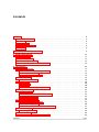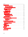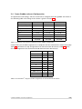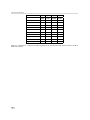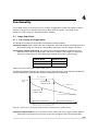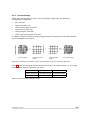
1
User Manual
DS1-D1312 CameraLink® Series
CMOS Area Scan Camera
MAN039 09/2009 V1.2
All information provided in this manual is believed to be accurate and reliable. No
responsibility is assumed by Photonfocus AG for its use. Photonfocus AG reserves the right to
make changes to this information without notice.
Reproduction of this manual in whole or in part, by any means, is prohibited without prior
permission having been obtained from Photonfocus AG.
1
2
Contents
1 Preface
1.1 About Photonfocus
1.2 Contact . . . . . . .
1.3 Sales Offices . . . .
1.4 Further information
1.5 Legend . . . . . . .
.
.
.
.
.
.
.
.
.
.
.
.
.
.
.
.
.
.
.
.
.
.
.
.
.
.
.
.
.
.
.
.
.
.
.
.
.
.
.
.
.
.
.
.
.
.
.
.
.
.
.
.
.
.
.
.
.
.
.
.
.
.
.
.
.
.
.
.
.
.
.
.
.
.
.
.
.
.
.
.
.
.
.
.
.
.
.
.
.
.
.
.
.
.
.
.
.
.
.
.
.
.
.
.
.
.
.
.
.
.
.
.
.
.
.
.
.
.
.
.
.
.
.
.
.
.
.
.
.
.
.
.
.
.
.
.
.
.
.
.
.
.
.
.
.
.
.
.
.
.
.
.
.
.
.
.
.
.
.
.
.
.
.
.
.
.
.
.
.
.
.
.
.
.
.
.
.
.
.
.
.
.
.
.
.
5
5
5
5
5
6
.
.
.
.
.
2 How to get started (CameraLink® )
3 Product Specification
3.1 Introduction . . . . . . . . . . . . . . . .
3.2 Feature Overview . . . . . . . . . . . . .
3.3 Technical Specification . . . . . . . . . .
3.4 Frame Grabber relevant Configuration .
7
.
.
.
.
.
.
.
.
.
.
.
.
.
.
.
.
.
.
.
.
.
.
.
.
.
.
.
.
.
.
.
.
.
.
.
.
.
.
.
.
.
.
.
.
.
.
.
.
.
.
.
.
.
.
.
.
.
.
.
.
.
.
.
.
.
.
.
.
.
.
.
.
.
.
.
.
.
.
.
.
.
.
.
.
.
.
.
.
.
.
.
.
11
11
12
13
15
4 Functionality
4.1 Image Acquisition . . . . . . . . . . . . . . . . .
4.1.1 Free-running and Trigger Mode . . . . .
4.1.2 Exposure Control . . . . . . . . . . . . .
4.1.3 Maximum Frame Rate . . . . . . . . . .
4.2 Pixel Response . . . . . . . . . . . . . . . . . . .
4.2.1 Linear Response . . . . . . . . . . . . . .
4.3 Test Images . . . . . . . . . . . . . . . . . . . . .
4.3.1 Ramp . . . . . . . . . . . . . . . . . . . .
4.3.2 LFSR . . . . . . . . . . . . . . . . . . . . .
4.3.3 Troubleshooting using the LFSR . . . . .
4.4 Image Correction . . . . . . . . . . . . . . . . .
4.4.1 Overview . . . . . . . . . . . . . . . . . .
4.4.2 Offset Correction (FPN, Hot Pixels) . . .
4.4.3 Gain Correction . . . . . . . . . . . . . .
4.4.4 Corrected Image . . . . . . . . . . . . . .
4.5 Reduction of Image Size . . . . . . . . . . . . .
4.5.1 Region of Interest (ROI) . . . . . . . . .
4.5.2 ROI configuration . . . . . . . . . . . . .
4.5.3 Calculation of the maximum frame rate
4.6 External Trigger . . . . . . . . . . . . . . . . . .
4.6.1 Trigger Source . . . . . . . . . . . . . . .
4.7 Strobe Output . . . . . . . . . . . . . . . . . . .
4.8 Configuration Interface (CameraLink® ) . . . .
.
.
.
.
.
.
.
.
.
.
.
.
.
.
.
.
.
.
.
.
.
.
.
.
.
.
.
.
.
.
.
.
.
.
.
.
.
.
.
.
.
.
.
.
.
.
.
.
.
.
.
.
.
.
.
.
.
.
.
.
.
.
.
.
.
.
.
.
.
.
.
.
.
.
.
.
.
.
.
.
.
.
.
.
.
.
.
.
.
.
.
.
.
.
.
.
.
.
.
.
.
.
.
.
.
.
.
.
.
.
.
.
.
.
.
.
.
.
.
.
.
.
.
.
.
.
.
.
.
.
.
.
.
.
.
.
.
.
.
.
.
.
.
.
.
.
.
.
.
.
.
.
.
.
.
.
.
.
.
.
.
.
.
.
.
.
.
.
.
.
.
.
.
.
.
.
.
.
.
.
.
.
.
.
.
.
.
.
.
.
.
.
.
.
.
.
.
.
.
.
.
.
.
.
.
.
.
.
.
.
.
.
.
.
.
.
.
.
.
.
.
.
.
.
.
.
.
.
.
.
.
.
.
.
.
.
.
.
.
.
.
.
.
.
.
.
.
.
.
.
.
.
.
.
.
.
.
.
.
.
.
.
.
.
.
.
.
.
.
.
.
.
.
.
.
.
.
.
.
.
.
.
.
.
.
.
.
.
.
.
.
.
.
.
.
.
.
.
.
.
.
.
.
.
.
.
.
.
.
.
.
.
.
.
.
.
.
.
.
.
.
.
.
.
.
.
.
.
.
.
.
.
.
.
.
.
.
.
.
.
.
.
.
.
.
.
.
.
.
.
.
.
.
.
.
.
.
.
.
.
.
.
.
.
.
.
.
.
.
.
.
.
.
.
.
.
.
.
.
.
.
.
.
.
.
.
.
.
.
.
.
.
.
.
.
.
.
.
.
.
.
.
.
.
.
.
.
.
.
.
.
.
.
.
.
.
.
.
.
.
.
.
.
.
.
.
.
.
.
.
.
.
.
.
.
.
.
.
.
.
.
.
.
.
.
.
.
.
.
.
.
.
.
.
.
.
.
.
.
.
.
.
.
.
.
.
.
.
.
.
.
.
.
.
.
.
.
.
.
.
.
.
.
.
.
.
.
.
.
.
.
.
.
.
.
.
.
.
.
.
.
.
.
.
.
.
17
17
17
19
19
19
19
20
20
20
20
23
23
23
25
27
28
28
30
31
34
34
34
34
CONTENTS
.
.
.
.
.
.
.
.
.
.
.
.
3
CONTENTS
5 Hardware Interface
5.1 Connectors . . . . . . . . . . . . . . .
5.1.1 CameraLink® Connector . . .
5.1.2 Power Supply . . . . . . . . .
5.1.3 Trigger and Strobe Signals . .
5.1.4 Status Indicator (CameraLink®
5.2 CameraLink® Data Interface . . . . .
5.3 Read-out Timing . . . . . . . . . . . .
5.3.1 Free running Mode . . . . . .
5.4 Trigger . . . . . . . . . . . . . . . . .
5.4.1 Trigger Modes . . . . . . . . .
5.4.2 Trigger Delay . . . . . . . . . .
. . . . . .
. . . . . .
. . . . . .
. . . . . .
cameras)
. . . . . .
. . . . . .
. . . . . .
. . . . . .
. . . . . .
. . . . . .
.
.
.
.
.
.
.
.
.
.
.
.
.
.
.
.
.
.
.
.
.
.
.
.
.
.
.
.
.
.
.
.
.
.
.
.
.
.
.
.
.
.
.
.
.
.
.
.
.
.
.
.
.
.
.
.
.
.
.
.
.
.
.
.
.
.
.
.
.
.
.
.
.
.
.
.
.
.
.
.
.
.
.
.
.
.
.
.
.
.
.
.
.
.
.
.
.
.
.
.
.
.
.
.
.
.
.
.
.
.
.
.
.
.
.
.
.
.
.
.
.
.
.
.
.
.
.
.
.
.
.
.
.
.
.
.
.
.
.
.
.
.
.
.
.
.
.
.
.
.
.
.
.
.
.
.
.
.
.
.
.
.
.
.
.
.
.
.
.
.
.
.
.
.
.
.
.
.
.
.
.
.
.
.
.
.
.
.
.
.
.
.
.
.
.
.
.
.
.
.
.
.
.
.
.
.
.
.
.
.
.
.
.
.
.
.
.
.
.
.
.
.
.
.
.
.
.
.
.
.
.
.
.
.
.
.
.
.
.
.
.
.
37
37
37
37
38
38
39
41
41
44
44
44
6 The PFRemote Control Tool
6.1 Overview . . . . . . . . . . . . . .
6.2 PFRemote and PFLib . . . . . . .
6.3 Operating System . . . . . . . . .
6.4 Installation Notes . . . . . . . . .
6.5 Graphical User Interface (GUI) . .
6.5.1 Port Browser . . . . . . . .
6.5.2 Ports, Device Initialization
6.5.3 Main Buttons . . . . . . .
6.6 Device Properties . . . . . . . . .
.
.
.
.
.
.
.
.
.
.
.
.
.
.
.
.
.
.
.
.
.
.
.
.
.
.
.
.
.
.
.
.
.
.
.
.
.
.
.
.
.
.
.
.
.
.
.
.
.
.
.
.
.
.
.
.
.
.
.
.
.
.
.
.
.
.
.
.
.
.
.
.
.
.
.
.
.
.
.
.
.
.
.
.
.
.
.
.
.
.
.
.
.
.
.
.
.
.
.
.
.
.
.
.
.
.
.
.
.
.
.
.
.
.
.
.
.
.
.
.
.
.
.
.
.
.
.
.
.
.
.
.
.
.
.
.
.
.
.
.
.
.
.
.
.
.
.
.
.
.
.
.
.
.
.
.
.
.
.
.
.
.
.
.
.
.
.
.
.
.
.
.
.
.
.
.
.
.
.
.
.
.
.
.
.
.
.
.
.
.
.
.
.
.
.
.
.
.
.
.
.
.
.
.
.
.
.
47
47
47
47
47
48
48
49
50
50
7 Graphical User Interface (GUI)
7.1 DS1-D1312-40, DS1-D1312-80 and DS1-D1312-160
7.1.1 Exposure, Window . . . . . . . . . . . . . .
7.1.2 Trigger . . . . . . . . . . . . . . . . . . . . .
7.1.3 Correction . . . . . . . . . . . . . . . . . . .
7.1.4 Info . . . . . . . . . . . . . . . . . . . . . . .
.
.
.
.
.
.
.
.
.
.
.
.
.
.
.
.
.
.
.
.
.
.
.
.
.
.
.
.
.
.
.
.
.
.
.
.
.
.
.
.
.
.
.
.
.
.
.
.
.
.
.
.
.
.
.
.
.
.
.
.
.
.
.
.
.
.
.
.
.
.
.
.
.
.
.
.
.
.
.
.
.
.
.
.
.
.
.
.
.
.
.
.
.
.
.
.
.
.
.
.
51
51
52
53
54
56
8 Mechanical and Optical Considerations
8.1 Mechanical Interface . . . . . . . . . . . . . .
8.1.1 Cameras with CameraLink® Interface
8.2 Optical Interface . . . . . . . . . . . . . . . . .
8.2.1 Cleaning the Sensor . . . . . . . . . . .
8.3 Compliance . . . . . . . . . . . . . . . . . . . .
.
.
.
.
.
.
.
.
.
.
.
.
.
.
.
.
.
.
.
.
.
.
.
.
.
.
.
.
.
.
.
.
.
.
.
.
.
.
.
.
.
.
.
.
.
.
.
.
.
.
.
.
.
.
.
.
.
.
.
.
.
.
.
.
.
.
.
.
.
.
.
.
.
.
.
.
.
.
.
.
.
.
.
.
.
.
.
.
.
.
.
.
.
.
.
.
.
.
.
.
57
57
57
58
58
60
.
.
.
.
.
.
.
.
.
.
.
.
.
.
.
.
.
.
.
.
.
.
.
.
.
.
.
.
.
.
.
.
.
.
.
.
.
.
.
.
.
.
.
.
.
.
.
.
.
.
.
.
.
.
.
.
.
.
.
.
.
.
.
.
.
.
.
.
.
.
.
.
.
.
.
.
.
.
9 Warranty
61
9.1 Warranty Terms . . . . . . . . . . . . . . . . . . . . . . . . . . . . . . . . . . . . . . . . 61
9.2 Warranty Claim . . . . . . . . . . . . . . . . . . . . . . . . . . . . . . . . . . . . . . . . 61
10 References
63
A Pinouts
65
A.1 Power Supply Connector . . . . . . . . . . . . . . . . . . . . . . . . . . . . . . . . . . . 65
A.2 CameraLink® Connector . . . . . . . . . . . . . . . . . . . . . . . . . . . . . . . . . . . 66
B Revision History
4
69
1
Preface
1.1
About Photonfocus
The Swiss company Photonfocus is one of the leading specialists in the development of CMOS
image sensors and corresponding industrial cameras for machine vision, security & surveillance
and automotive markets.
Photonfocus is dedicated to making the latest generation of CMOS technology commercially
available. Active Pixel Sensor (APS) and global shutter technologies enable high speed and
high dynamic range (120 dB) applications, while avoiding disadvantages like image lag,
blooming and smear.
Photonfocus has proven that the image quality of modern CMOS sensors is now appropriate
for demanding applications. Photonfocus’ product range is complemented by custom design
solutions in the area of camera electronics and CMOS image sensors.
Photonfocus is ISO 9001 certified. All products are produced with the latest techniques in order
to ensure the highest degree of quality.
1.2
Contact
Photonfocus AG, Bahnhofplatz 10, CH-8853 Lachen SZ, Switzerland
Sales
Phone: +41 55 451 07 45
Email: [email protected]
Support
Phone: +41 55 451 01 37
Email: [email protected]
Table 1.1: Photonfocus Contact
1.3
Sales Offices
Photonfocus products are available through an extensive international distribution network
and through our key account managers. Details of the distributor nearest you and contacts to
our key account managers can be found at www.photonfocus.com.
1.4
Further information
Photonfocus reserves the right to make changes to its products and documentation without notice. Photonfocus products are neither intended nor certified for
use in life support systems or in other critical systems. The use of Photonfocus
products in such applications is prohibited.
Photonfocus is a trademark and LinLog® is a registered trademark of Photonfocus AG. CameraLink® and GigE Vision® are a registered mark of the Automated
Imaging Association. Product and company names mentioned herein are trademarks or trade names of their respective companies.
5
1 Preface
Reproduction of this manual in whole or in part, by any means, is prohibited
without prior permission having been obtained from Photonfocus AG.
Photonfocus can not be held responsible for any technical or typographical errors.
1.5
Legend
In this documentation the reader’s attention is drawn to the following icons:
Important note
Alerts and additional information
Attention, critical warning
✎
6
Notification, user guide
2
How to get started (CameraLink® )
1.
Install a suitable frame grabber in your PC.
To find a compliant frame grabber, please see the frame grabber compatibility
list at www.photonfocus.com.
2.
Install the frame grabber software.
✎
3.
Without installed frame grabber software the camera configuration tool PFRemote will not be able to communicate with the camera. Please follow the instructions of the frame grabber supplier.
Remove the camera from its packaging. Please make sure the following items are included
with your camera:
•
Power supply connector (7-pole power plug)
•
Camera body cap
If any items are missing or damaged, please contact your dealership.
4.
Remove the camera body cap from the camera and mount a suitable lens.
When removing the camera body cap or when changing the lens, the camera
should always be held with the opening facing downwards to prevent dust or
debris falling onto the CMOS sensor.
Figure 2.1: Camera with protective cap and lens.
Do not touch the sensor surface. Protect the image sensor from particles and
dirt!
7
2 How to get started (CameraLink® )
The sensor has no cover glass, therefore dust on the sensor surface may resemble
to clusters or extended regions of dead pixel.
To choose a lens, see
www.photonfocus.com.
5.
the
Lens
Finder
in
the
’Support’
area
at
Connect the camera to the frame grabber with a suitable CameraLink® cable (see Fig. 2.2).
CameraLink® cables can be purchased from Photonfocus directly (www.photonfocus.com).
Please note that Photonfocus provides appropriate solutions for your advanced vision
applications.
Figure 2.2: Camera with frame grabber, power supply and cable.
Do not connect or disconnect the CameraLink® cable while camera power is on!
For more information about CameraLink® see Section 4.8.
6.
Connect a suitable power supply to the provided 7-pole power plug. For the connector
assembly see Fig. A.1. The pinout of the connector is shown in Appendix A.
Check the correct supply voltage and polarity! Do not exceed the maximum
operating voltage of +12V DC (± 10%).
7.
Connect the power supply to the camera (see Fig. 2.2).
✎
8
The status LED on the rear of the camera will light red for a short moment, and
then flash green. For more information see Section 5.1.4.
8.
Download the camera software PFRemote to your computer.
You can find the latest version of PFRemote on the support page at
www.photonfocus.com.
9.
Install the camera software PFRemote. Please follow the instructions of the PFRemote
setup wizard.
Figure 2.3: Screen shot PFremote setup wizard
10. Start the camera software PFRemote and choose the communication port.
Figure 2.4: PFRemote start window
11. Check the status LED on the rear of the camera.
✎
The status LED lights green when an image is being produced, and it is red when
serial communication is active. For more information see Section 5.1.4.
12. You may display images using the software that is provided by the frame grabber
manufacturer.
9
2 How to get started (CameraLink® )
10
3
Product Specification
3.1
Introduction
The DS1-D1312 camera series is built around the monochrome A1312 CMOS image sensor from
Photonfocus, that provides a resolution of 1312 x 1082 pixels at a wide range of spectral
sensitivity. It is aimed at standard applications in industrial image processing. The principal
advantages are:
•
Resolution of 1312 x 1082 pixels.
•
Superior signal-to-noise ratio.
•
Low power consumption at high speeds.
•
Very high resistance to blooming.
•
High dynamic range of up to 60 dB.
•
Ideal for high speed applications: Global shutter.
•
Greyscale resolution of up to 10 bit.
•
On camera shading correction.
•
Software provided for setting and storage of camera parameters.
•
The camera has a digital CameraLink® interface.
•
The compact size make the DS1-D1312 camera the perfect solution for applications in
which space is at a premium.
•
Wide spectral sensitivity from 320 to 1030 nm.
•
High quantum efficiency (> 50%).
•
High pixel fill factor (> 60%).
The general specification and features of the camera is listed in the following sections.
.
11
3 Product Specification
3.2
Feature Overview
Characteristics
Interfaces
Camera Control
Configuration Interface
Trigger Modes
Features
DS1-D1312 Series
CameraLink® base configuration
PFRemote (Windows GUI) or programming library
CLSERIAL (9’600 baud)
Interface Trigger / External opto isolated trigger input
Greyscale resolution 10 bit / 8 bit
Region of Interest (ROI)
Test pattern (LFSR and grey level ramp)
Shading Correction (Offset and Gain)
High blooming resistance
Opto isolated trigger input and opto isolated strobe output
Table 3.1: Feature overview (see Chapter 4 for more information)
Figure 3.1: DS1-D1312 CMOS camera series with C-mount lens.
.
12
3.3
Technical Specification
Technical Parameters
DS1-D1312- Series
Technology
CMOS active pixel (APS)
Scanning system
Optical format / diagonal
Progressive scan
1” (13.6 mm diagonal) @ maximum resolution
2/3” (11.6 mm diagonal) @ 1024 x 1024 resolution
Resolution
1312 x 1082 pixels
Pixel size
8 µm x 8 µm
Active optical area
10.48 mm x 8.64 mm (maximum)
< 0.3 DN @ 8 bit 1)
Random noise
Fixed pattern noise (FPN)
3.4 DN @ 8 bit / correction OFF 1)
Fixed pattern noise (FPN)
< 1DN @ 8 bit / correction ON 1)2)
Dark current
0.65 fA / pixel @ 27 °C
~ 100 ke−
Full well capacity
Spectral range
320 nm to 1030 nm (to 10% of peak responsivity)
210 x103 DN/(J/m2 ) @ 625 nm / 8 bit
Responsivity
Quantum Efficiency
> 50 %
Optical fill factor
> 60 %
Dynamic range
Up to 60 dB
Colour format
Monochrome
Characteristic curve
Linear
Shutter mode
Global shutter
Greyscale resolution
10 bit / 8 bit
Exposure Time
10 µs ... 0.41 s
Table 3.2: General specification of the DS1-D1312 camera series (Footnotes:
values. 2) Indicated values are subject to confirmation.)
Exposure Time
Exposure time increment
3)
Frame rate
( Tint = 10 µs)
Pixel clock frequency
Pixel clock cycle
Indicated values are typical
DS1-D1312-40
DS1-D1312-80
DS1-D1312-160
10 µs ... 1.68 s
10 µs ... 0.84 s
10 µs ... 0.42 s
100 ns
50 ns
25 ns
27 fps
54 fps
108 fps
40 MHz
40 MHz
80 MHz
25 ns
25 ns
12.5 ns
1
2
2
Camera taps
Read out mode
Table 3.3: Model-specific parameters (Footnote:
3.3 Technical Specification
1)
sequential or simultaneous
3)
Maximum frame rate @ full resolution)
13
3 Product Specification
DS1-D1312-40
DS1-D1312-80
Operating temperature
DS1-D1312-160
0°C ... 50°C
Camera power supply
+12 V DC (± 10 %)
Trigger signal input range
+5 .. +15 V DC
Max. power consumption
< 2.5 W
< 3.0 W
< 3.3 W
Lens mount
C-Mount (CS-Mount optional)
Dimensions
60 x 60 x 45 mm3
Mass
265 g
Conformity
CE / RoHS / WEE
Table 3.4: Physical characteristics and operating ranges
Fig. 3.2 shows the quantum efficiency and the responsivity of the A1312 sensor, displayed as a
function of wavelength. For more information on photometric and radiometric measurements
see the Photonfocus application notes AN006 and AN008 available in the support area of our
website www.photonfocus.com.
60%
QE
1200
Responsivity
50%
1000
800
30%
600
20%
400
10%
200
0%
200
0
300
400
500
600
700
800
900
Wavelength [nm]
Figure 3.2: Spectral response of the A1312 sensor in the DS1-D1312 camera series
.
14
1000
1100
Responsivity [V
V/J/m²]
Quantum
m Efficiency
40%
3.4
Frame Grabber relevant Configuration
The parameters and settings, which are essential to configure the frame grabber are shown in
the following table. The timing of the camera is given in Section 5.3.
DS1-D1312-40
DS1-D1312-80
DS1-D1312-160
40 MHz
40 MHz
80 MHz
1
2
2
10 bit / 8 bit
10 bit / 8 bit
10 bit / 8 bit
36 clock cycles
18 clock cycles
18 clock cycles
CC1
EXSYNC
EXSYNC
EXSYNC
CC2
not used
not used
not used
CC3
not used
not used
not used
CC4
not used
not used
not used
Pixel Clock per Tap
Number of Taps
Greyscale resolution
Line pause
Table 3.5: Summary of parameters needed for frame grabber configuration
CameraLink® port and bit assignments are compliant with the CameraLink® standard (see [CL]).
Table 3.6 summarizes the tap configurations for the DS1-D1312-40 cameras. Table 3.7 shows
the tap configurations for the DS1-D1312-80 and DS1-D1312-160 cameras.
Bit
Tap 0
Tap 0
8 Bit
10 Bit
0 (LSB)
A0
A0
1
A1
A1
2
A2
A2
3
A3
A3
4
A4
A4
5
A5
A5
6
A6
A6
7 (MSB of 8 Bit)
A7
A7
8
-
B0
9 (MSB of 10 Bit)
-
B1
Table 3.6: CameraLink® 1 Tap port and bit assignments for the DS1-D1312-40 camera
3.4 Frame Grabber relevant Configuration
15
3 Product Specification
Bit
Tap 0
Tap 1
Tap 0
Tap 1
8 Bit
8 Bit
10 Bit
10 Bit
0 (LSB)
A0
B0
A0
C0
1
A1
B1
A1
C1
2
A2
B2
A2
C2
3
A3
B3
A3
C3
4
A4
B4
A4
C4
5
A5
B5
A5
C5
6
A6
B6
A6
C6
7 (MSB of 8 Bit)
A7
B7
A7
C7
8
-
-
B0
B4
9 (MSB of 10 Bit)
-
-
B1
B5
Table 3.7: CameraLink® 2 Tap port and bit assignments for the DS1-D1312-80 camera and for the DS1D1312-160 camera
.
16
4
Functionality
This chapter serves as an overview of the camera configuration modes and explains camera
features. The goal is to describe what can be done with the camera. The setup of the
DS1-D1312 series cameras is explained in later chapters.
4.1
4.1.1
Image Acquisition
Free-running and Trigger Mode
The DS1-D1312 camera series provides two different readout modes:
Sequential readout Frame time is the sum of exposure time and readout time. Exposure time
of the next image can only start if the readout time of the current image is finished.
Simultaneous readout (interleave) The frame time is determined by the maximum of the
exposure time or of the readout time, which ever of both is the longer one. Exposure
time of the next image can start during the readout time of the current image.
Readout Mode
DS1-D1312 Series
Sequential readout
available
Simultaneous readout
available
Table 4.1: Readout mode of DS1-D1312 camera series
The following figure illustrates the effect on the frame rate when using either the sequential
readout mode or the simultaneous readout mode (interleave exposure).
fp s = 1 /r e a d o u t tim e
F ra m e ra te
(fp s)
S im u lta n e o u s
re a d o u t m o d e
fp s = 1 /e x p o s u r e tim e
S e q u e n tia l
re a d o u t m o d e
fp s = 1 /( r e a d o u t tim e + e x p o s u r e tim e )
e x p o s u re tim e < re a d o u t tim e
e x p o s u re tim e = re a d o u t tim e
e x p o s u re tim e > re a d o u t tim e
E x p o s u re tim e
Figure 4.1: Frame rate in sequential readout mode and simultaneous readout mode
Sequential readout mode For the calculation of the frame rate only a single formula applies:
frames per second equal to the invers of the sum of exposure time and readout time.
17
4 Functionality
Simultaneous readout mode (exposure time < readout time) The frame rate is given by the
readout time. Frames per second equal to the invers of the readout time.
Simultaneous readout mode (exposure time > readout time) The frame rate is given by the
exposure time. Frames per second equal to the invers of the exposure time.
The simultaneous readout mode allows higher frame rate. However, if the exposure time
strongly exceeds the readout time, then the effect on the frame rate is neglectable.
In simultaneous readout mode image output faces minor limitations. The overall
linear sensor reponse is partially restricted in the lower grey scale region.
When changing readout mode from sequential to simultaneous readout mode
or vice versa, new settings of the BlackLevelOffset and of the image correction
are required.
Sequential readout
By default the camera continuously delivers images as fast as possible ("Free-running mode")
in the sequential readout mode. Exposure time of the next image can only start if the readout
time of the current image is finished.
e x p o s u re
re a d o u t
e x p o s u re
re a d o u t
Figure 4.2: Timing in free-running sequential readout mode
When the acquisition of an image needs to be synchronised to an external event, an external
trigger can be used (refer to Section 4.6 and to Section 5.4). In this mode, the camera is idle
until it gets a signal to capture an image.
e x p o s u re
re a d o u t
id le
e x p o s u re
e x te r n a l tr ig g e r
Figure 4.3: Timing in triggered sequential readout mode
Simultaneous readout (interleave exposure)
To achieve highest possible frame rates, the camera must be set to "Free-running mode" with
simultaneous readout. The camera continuously delivers images as fast as possible. Exposure
time of the next image can start during the readout time of the current image.
e x p o s u re n
re a d o u t n -1
id le
e x p o s u re n + 1
re a d o u t n
id le
re a d o u t n + 1
fr a m e tim e
Figure 4.4: Timing in free-running simultaneous readout mode (readout time> exposure time)
18
e x p o s u re n -1
id le
e x p o s u re n + 1
e x p o s u re n
re a d o u t n -1
id le
re a d o u t n
fr a m e tim e
Figure 4.5: Timing in free-running simultaneous readout mode (readout time< exposure time)
When the acquisition of an image needs to be synchronised to an external event, an external
trigger can be used (refer to 4.6 and 5.4). In this mode, the camera is idle until it gets a signal
to capture an image.
Figure 4.6: Timing in triggered simultaneous readout mode
4.1.2
Exposure Control
The exposure time defines the period during which the image sensor integrates the incoming
light. Refer to Section Table 3.3 for the allowed exposure time range.
4.1.3
Maximum Frame Rate
The maximum frame rate depends on the exposure time and the size of the image (see 4.5.)
4.2
4.2.1
Pixel Response
Linear Response
The camera offers a linear response between input light signal and output grey level. In
addition, a linear digital gain may be applied, as follows. Please see Table 3.2 for more
model-dependent information.
Gain x1
The DS1-D1312 camera series supports gain x1 only.
4.2 Pixel Response
19
4 Functionality
Black Level Adjustment
The black level is the average image value at no light intensity. It can be adjusted by the
software by changing the black level offset. Thus, the overall image gets brighter or darker.
Use a histogram to check the settings of the black level.
4.3
Test Images
Test images are generated in the camera FPGA, independent of the image sensor. They can be
used to check the transmission path from the camera to the frame grabber. Independent from
the configured grey level resolution, every possible grey level appears the same number of
times in a test image. Therefore, the histogram of the received image must be flat.
A test image is a useful tool to find data transmission errors that are caused most
often by a defective cable between camera and frame grabber.
The analysis of the test images with a histogram tool gives the correct result at
full resolution only.
4.3.1
Ramp
Depending on the configured grey level resolution, the ramp test image outputs a constant
pattern with increasing grey level from the left to the right side (see Fig. 4.7).
Figure 4.7: Ramp test images: 8 bit output (left), 10 bit output (right)
4.3.2
LFSR
The LFSR (linear feedback shift register) test image outputs a constant pattern with a
pseudo-random grey level sequence containing every possible grey level that is repeated for
every row. The LFSR test pattern was chosen because it leads to a very high data toggling rate,
which stresses the interface electronic and the cable connection.
In the histogram you can see that the number of pixels of all grey values are the same.
Please refer to application note [AN026] for the calculation and the values of the LFSR test
image.
4.3.3
Troubleshooting using the LFSR
To control the quality of your complete imaging system enable the LFSR mode and check the
histogram at full resolution. If your frame grabber application does not provide a real-time
histogram, store the image and use a graphic software tool to display the histogram.
20
Figure 4.8: LFSR (linear feedback shift register) test image
In the LFSR (linear feedback shift register) mode the camera generates a constant
pseudo-random test pattern containing all grey levels. If the data transmission is error free, the
histogram of the received LFSR test pattern will be flat (Fig. 4.9). On the other hand, a non-flat
histogram (Fig. 4.10) indicates problems, that may be caused either by the cable, by the
connectors or by the frame grabber.
A possible origin of failure message can be caused by the CameraLink® cable
which exceeds the maximum length. Also, CameraLink® cables may suffer either
from stress due to wrong installation or from severe electromagnetic interference.
.
4.3 Test Images
21
4 Functionality
Some thinner CameraLink® cables have a predefined direction. In these cables
not all twisted pairs are separately shielded to meet the RS644 standard. These
pairs are used for the transmission of the RX/TX and for the CC1 to CC4 low
frequency control signals.
Figure 4.9: LFSR test pattern received at the frame grabber and typical histogram for error-free data
transmission
Figure 4.10: LFSR test pattern received at the frame grabber and histogram containing transmission errors
CameraLink® cables contain wire pairs, which are twisted in such a way that the
cable impedance matches with the LVDS driver and receiver impedance. Excess
stress on the cable results in transmission errors which causes distorted images.
Therefore, please do not stretch and bend a CameraLink cable.
In robots applications, the stress that is applied to the CameraLink® cable is especially high due
to the fast movement of the robot arm. For such applications, special drag chain capable cables
are available. Please contact the Photonfocus Support for consulting expertise. Appropriate
CameraLink® cable solutions are available from Photonfocus.
.
22
4.4
Image Correction
4.4.1
Overview
The camera possesses image pre-processing features, that compensate for non-uniformities
caused by the sensor, the lens or the illumination. This method of improving the image quality
is generally known as ’Shading Correction’ or ’Flat Field Correction’ and consists of a
combination of offset correction, gain correction and pixel interpolation.
Since the correction is performed in hardware, there is no performance limitation of the cameras for high frame rates.
The offset correction subtracts a configurable positive or negative value from the live image
and thus reduces the fixed pattern noise of the CMOS sensor. In addition, hot pixels can be
removed by interpolation. The gain correction can be used to flatten uneven illumination or to
compensate shading effects of a lens. Both offset and gain correction work on a pixel-per-pixel
basis, i.e. every pixel is corrected separately. For the correction, a black reference and a grey
reference image are required. Then, the correction values are determined automatically in the
camera.
Do not set any reference images when gain or LUT is enabled! Read the following sections very carefully.
Correction values of both reference images can be saved into the internal flash memory, but
this overwrites the factory presets. Then the reference images that are delivered by factory
cannot be restored anymore.
4.4.2
Offset Correction (FPN, Hot Pixels)
The offset correction is based on a black reference image, which is taken at no illumination
(e.g. lens aperture completely closed). The black reference image contains the fixed-pattern
noise of the sensor, which can be subtracted from the live images in order to minimise the
static noise.
Offset correction algorithm
After configuring the camera with a black reference image, the camera is ready to apply the
offset correction:
1.
Determine the average value of the black reference image.
2.
Subtract the black reference image from the average value.
3.
Mark pixels that have a grey level higher than 252 DN (@ 10 bit) as hot pixels.
4.
Store the result in the camera as the offset correction matrix.
5.
During image acquisition, subtract the correction matrix from the acquired image and
interpolate the hot pixels (see Section 4.4.2).
4.4 Image Correction
23
4 Functionality
1
4
3
1
4
1
4
2
4
2
4
3
4
2
3
1
1
1
3
4
3
1
3
4
4
-
b la c k r e fe r e n c e
im a g e
a v e ra
o f b la
re fe re
p ic tu
g e
c k
n c e
re
=
1
1
1
-2
1
1
-1
2
-1
1
-1
0
1
-1
2
0
-2
0
2
-2
0
0
-1
-2
-2
o ffs e t c o r r e c tio n
m a tr ix
Figure 4.11: Schematic presentation of the offset correction algorithm
How to Obtain a Black Reference Image
In order to improve the image quality, the black reference image must meet certain demands.
•
The black reference image must be obtained at no illumination, e.g. with lens aperture
closed or closed lens opening.
•
It may be necessary to adjust the black level offset of the camera. In the histogram of the
black reference image, ideally there are no grey levels at value 0 DN after adjustment of
the black level offset. All pixels that are saturated black (0 DN) will not be properly
corrected (see Fig. 4.12). The peak in the histogram should be well below the hot pixel
threshold of 252 DN @ 10 bit.
•
Camera settings may influence the grey level. Therefore, for best results the camera
settings of the black reference image must be identical with the camera settings of the
image to be corrected.
Figure 4.12: Histogram of a proper black reference image for offset correction
Hot pixel correction
Every pixel that exceeds a certain threshold in the black reference image is marked as a hot
pixel. If the hot pixel correction is switched on, the camera replaces the value of a hot pixel by
an average of its neighbour pixels (see Fig. 4.13).
24
p
h o t
p ix e l
n -1
p
n
p
p
n
=
p
n -1
+ p
2
n + 1
n + 1
Figure 4.13: Hot pixel interpolation
4.4.3
Gain Correction
The gain correction is based on a grey reference image, which is taken at uniform illumination
to give an image with a mid grey level.
Gain correction is not a trivial feature. The quality of the grey reference image
is crucial for proper gain correction.
Gain correction algorithm
After configuring the camera with a black and grey reference image, the camera is ready to
apply the gain correction:
1.
Determine the average value of the grey reference image.
2.
Subtract the offset correction matrix from the grey reference image.
3.
Divide the average value by the offset corrected grey reference image.
4.
Pixels that have a grey level higher than a certain threshold are marked as hot pixels.
5.
Store the result in the camera as the gain correction matrix.
6.
During image acquisition, multiply the gain correction matrix from the offset-corrected
acquired image and interpolate the hot pixels (see Section 4.4.2).
Gain correction is not a trivial feature. The quality of the grey reference image
is crucial for proper gain correction.
4.4 Image Correction
25
4 Functionality
a v e
o f
re fe
p ic
ra
g r
re
tu
g e
a y
n c e
re
:
1
4
3
1
4
4
8
7
9
9
6
7
7
9
2
7
3
1 0
8
9
3
1 0
4
6
1
g ra y re fe re n c e
p ic tu r e
-
1
1
1
-2
1
1
-1
2
-1
1
-1
0
1
-1
2
0
-2
0
0
2
-2
0
-1
-2
-2
o ffs e t c o r r e c tio n
m a tr ix
)
=
1
1
1
0 .9
-2
1 .2
1
1
1
0 .9
0
-1
1
1
1 .2 0 .8
1
-2
1
-2
0
0 .8
1 .3
1
-2
g a in c o r r e c tio n
m a tr ix
Figure 4.14: Schematic presentation of the gain correction algorithm
Gain correction always needs an offset correction matrix. Thus, the offset correction always has to be performed before the gain correction.
How to Obtain a Grey Reference Image
In order to improve the image quality, the grey reference image must meet certain demands.
•
The grey reference image must be obtained at uniform illumination.
Use a high quality light source that delivers uniform illumination. Standard illumination will not be appropriate.
•
When looking at the histogram of the grey reference image, ideally there are no grey
levels at full scale (1023 DN @ 10 bit). All pixels that are saturated white will not be
properly corrected (see Fig. 4.15).
•
Camera settings may influence the grey level. Therefore, the camera settings of the grey
reference image must be identical with the camera settings of the image to be corrected.
Figure 4.15: Proper grey reference image for gain correction
26
4.4.4
Corrected Image
Offset, gain and hot pixel correction can be switched on separately. The following
configurations are possible:
•
No correction
•
Offset correction only
•
Offset and hot pixel correction
•
Hot pixel correction only
•
Offset and gain correction
•
Offset, gain and hot pixel correction
)
In addition, the black reference image and grey reference image that are currently stored in
the camera RAM can be output.
1
4
3
7
4
5
4
7
6
7
6
4
5
6
3
7
6
6
5
3
7
1
c u r r e n t im a g e
4
3
4
-
1
1
1
-2
1
1
-1
2
-1
1
-1
0
1
-1
2
0
-2
0
0
0
-1
-2
2
-2
-2
o ffs e t c o r r e c tio n
m a tr ix
.
1
1
1
0 .9
-2
1 .2
1
1
1
0 .9
-1
1
1
0
1 .2 0 .8
1
-2
1
1
4
0
-2
0 .8
1 .3
1
=
-2
g a in c o r r e c tio n
m a tr ix
3
7
5
4
4
7
5
7
6
4
5
6
3
5
6
4
5
6
1
3
3
4
4
c o r r e c te d im a g e
Figure 4.16: Schematic presentation of the corrected image using gain correction algorithm
Table 4.2 shows the minimum and maximum values of the correction matrices, i.e. the range
that the offset and gain algorithm can correct.
Offset correction
Minimum
Maximum
-127 DN @ 10 bit
+127 DN @ 10 bit
0.42
2.67
Gain correction
Table 4.2: Offset and gain correction ranges
.
4.4 Image Correction
27
4 Functionality
4.5
Reduction of Image Size
With Photonfocus cameras there are several possibilities to focus on the interesting parts of an
image, thus reducing the data rate and increasing the frame rate. The most commonly used
feature is Region of Interest (ROI).
4.5.1
Region of Interest (ROI)
Some applications do not need full image resolution (e.g. 1312 x 1082 pixels). By reducing the
image size to a certain region of interest (ROI), the frame rate can be drastically increased. A
region of interest can be almost any rectangular window and is specified by its position within
the full frame and its width (W) and height (H). Fig. 4.17, Fig. 4.18 and Fig. 4.19 show possible
configurations for the region of interest, and Table 4.3 presents numerical examples of how
the frame rate can be increased by reducing the ROI.
Both reductions in x- and y-direction result in a higher frame rate.
The minimum width of the region of interest depends on the model of the DS1D1312 camera series. For more details please consult Table 4.4 and Table 4.5.
The minimum width must be positioned symmetrically towards the vertical center line of the sensor as shown in Fig. 4.17, Fig. 4.18 and Fig. 4.19). A list of
possible settings of the ROI for each camera model is given in Table 4.5.
³ 1 4 4 P ix e l
³ 1 4 4 P ix e l + m o d u lo 3 2 P ix e l
³ 1 4 4 P ix e l
³ 1 4 4 P ix e l
+ m o d u lo 3 2 P ix e l
a )
b )
Figure 4.17: Possible configuration of the region of interest for the DS1-D1312-40 CMOS camera
✎
28
It is recommended to re-adjust the settings of the shading correction each time
a new region of interest is selected.
³ 2 0 8 P ix e l
³ 2 0 8 P ix e l + m o d u lo 3 2 P ix e l
³ 2 0 8 P ix e l
³ 2 0 8 P ix e l
+ m o d u lo 3 2 P ix e l
b )
a )
Figure 4.18: Possible configuration of the region of interest with DS1-D1312-80 CMOS camera
³ 2 7 2 p ix e l
³ 2 7 2 p ix e l + m o d u lo 3 2 p ix e l
³ 2 7 2 p ix e l
³ 2 7 2 p ix e l
+ m o d u lo 3 2 p ix e l
a )
b )
Figure 4.19: Possible configuration of the region of interest with DS1-D1312-160 CMOS camera
Any region of interest may NOT be placed outside of the center of the sensor. Examples shown
in Fig. 4.20 illustrate configurations of the ROI that are NOT allowed.
.
4.5 Reduction of Image Size
29
4 Functionality
ROI Dimension [Standard]
DS1-D1312-40
DS1-D1312-80
DS1-D1312-160
1312 x 1082 (full resolution)
27 fps
54 fps
108 fps
288 x 1 (minimum resolution)
10245 fps
10863 fps
not allowed ROI setting
1280 x 1024 (SXGA)
29 fps
58 fps
117 fps
1280 x 768 (WXGA)
39 fps
78 fps
156 fps
800 x 600 (SVGA)
79 fps
157 fps
310 fps
640 x 480 (VGA)
121 fps
241 fps
472 fps
544 x 1
9615 fps
10498 fps
11022 fps
544 x 1082
63 fps
125 fps
249 fps
1312 x 544
54 fps
107 fps
214 fps
1312 x 256
114 fps
227 fps
445 fps
544 x 544
125 fps
248 fps
485 fps
1024 x 1024
36 fps
72 fps
145 fps
1312 x 1
8116 fps
9537 fps
10468 fps
Table 4.3: Frame rates of different ROI settings (exposure time 10 µs; correction on, and sequential readout
mode).
a )
b )
Figure 4.20: ROI configuration examples that are NOT allowed
4.5.2
ROI configuration
In the DS1-D1312 camera series the following two restrictions have to be respected for the ROI
configuration:
•
The minimum width (w) of the ROI is camera model dependent, consisting of 288 pixel in
the DS1-D1312-40 camera, of 416 pixel in the DS1-D1312-80 camera and of 544 pixel in the
DS1-D1312-80 camera.
•
The region of interest must overlap a minimum number of pixels centered to the left and
to the right of the vertical middle line of the sensor (ovl).
30
For any camera model of the DS1-D1312 camera series the allowed ranges for the ROI settings
can be deduced by the following formula:
xmin = max(0, 656 + ovl − w)
xmax = min(656 − ovl, 1312 − w)
.
where "ovl" is the overlap over the middle line and "w" is the width of the region of interest.
Any ROI settings in x-direction exceeding the minimum ROI width must be modulo 32.
ROI width (w)
overlap (ovl)
width condition
DS1-D1312-40
DS1-D1312-80
DS1-D1312-160
288 ... 1312
416 ... 1312
544 ... 1312
144
208
272
modulo 32
modulo 32
modulo 32
Table 4.4: Summary of the ROI configuration restrictions for the DS1-D1312 camera series indicating the
minimum ROI width (w) and the required number of pixel overlap (ovl) over the sensor middle line
The settings of the region of interest in x-direction are restricted to modulo 32
(see Table 4.5).
There are no restrictions for the settings of the region of interest in y-direction.
4.5.3
Calculation of the maximum frame rate
The frame rate mainly depends on the exposure time and readout time. The frame rate is the
inverse of the frame time.
1
fps = tframe
Calculation of the frame time (sequential mode)
tframe ≥ texp + tro
Typical values of the readout time tro are given in table Table 4.6. Calculation of the frame time
(simultaneous mode)
The calculation of the frame time in simultaneous read out mode requires more detailed data
input and is skipped here for the purpose of clarity.
✎
The formula for the calculation of the frame time in simultaneous mode is available from Photonfocus on request.
4.5 Reduction of Image Size
31
4 Functionality
Width
ROI-X (DS1-D1312-40)
ROI-X (DS1-D1312-80)
ROI-X (DS1-D1312-160)
288
512
not available
not available
320
480 ... 512
not available
not available
352
448 ... 512
not available
not available
384
416 ... 512
not available
not available
416
384 ... 512
448
not available
448
352 ... 512
416 ... 448
not available
480
320 ... 520
384 ... 448
not available
512
288 ... 512
352 ... 448
not available
544
256 ...512
320 ... 448
384
576
224 ... 512
288 ... 448
352 ... 384
608
192 ... 512
256 ... 448
320 ... 352
640
160 ... 512
224 ... 448
288 ... 384
672
128 ... 512
192 ... 448
256 ... 384
704
96 ... 512
160 ... 448
224 ... 384
736
64 ... 512
128 ... 448
192 ... 384
768
32 ... 512
96 ... 448
160 ... 384
800
0 ... 512
64 ... 448
128 ... 384
832
0 ... 480
32 ... 448
96 ... 384
864
0 ... 448
0 ... 448
64 ... 384
896
0 ... 416
0 ... 416
32 ... 384
...
...
...
...
1312
0
0
0
Table 4.5: Some possible ROI-X settings
ROI Dimension
DS1-D1312-40
DS1-D1312-80
DS1-D1312-160
1312 x 1082
tro = 36.46 ms
tro = 18.23 ms
tro = 9.12 ms
1024 x 512
tro = 13.57 ms
tro = 6.78 ms
tro = 3.39 ms
1024 x 256
tro = 6.78 ms
tro = 3.39 ms
tro = 1.70 ms
Table 4.6: Read out time at different ROI settings for the DS1-D1312 CMOS camera series in sequential
read out mode.
A frame rate calculator for calculating the maximum frame rate is available in
the support area of the Photonfocus website.
An overview of resulting frame rates in different exposure time settings is given in table Table
4.7.
.
32
Exposure time
DS1-D1312-40
DS1-D1312-80
DS1-D1312-160
10 µs
27 / 27 fps
54 / 54 fps
108 / 108 fps
100 µs
27 / 27 fps
54 / 54 fps
107 / 108 fps
500 µs
27 / 27 fps
53 / 54 fps
103 / 108 fps
1 ms
27 / 27 fps
51 / 54 fps
98 / 108 fps
2 ms
26 / 27 fps
49 / 54 fps
89 / 108 fps
5 ms
24 / 27 fps
42 / 54 fps
70 / 108 fps
10 ms
22 / 27 fps
35 / 54 fps
52 / 99 fps
12 ms
21 / 27 fps
33 / 54 fps
47 / 82 fps
Table 4.7: Frame rates of different exposure times, [sequential readout mode / simultaneous readout
mode], resolution 1312 x 1082 pixel (correction on).
4.5 Reduction of Image Size
33
4 Functionality
4.6
External Trigger
An external trigger is an event that starts an exposure. The trigger signal is either generated
on the frame grabber (soft-trigger) or comes from an external device such as a light barrier. If a
trigger signal is applied to the camera before the earliest time for the next trigger, this trigger
will be ignored.
4.6.1
Trigger Source
The trigger signal can be configured to be active high or active low. One of the following
trigger sources can be used:
Interface Trigger In the interface trigger mode, the trigger signal is applied to the camera by
the CameraLink® interface.
Trigger In the trigger mode, the trigger signal is applied directly to the camera by the power
supply connector (via an optocoupler).
C a m e r a
C L
I n t e r f a c e T r ig g e r
F r a m e g r a b b e r /
U S B h o s t
A n y T r ig g e r
S o u r c e
D A T A
o p t o
I n p u t
T r ig g e r I n p u t
A n y T r ig g e r
S o u r c e
Figure 4.21: Trigger Inputs
4.7
Strobe Output
The strobe output is an opto-isolated output located on the power supply connector that can
be used to trigger a strobe. The strobe output can be used both in free-running and in trigger
mode. There is a programmable delay available to adjust the strobe pulse to your application.
The strobe output needs a separate power supply. Please see Section 5.4 for
more information.
4.8
Configuration Interface (CameraLink® )
A CameraLink® camera can be controlled by the user via a RS232 compatible asynchronous
serial interface. This interface is contained within the CameraLink® interface as shown in Fig.
4.22 and is physically not directly accessible. Instead, the serial communication is usually routed
through the frame grabber. For some frame grabbers it might be necessary to connect a serial
cable from the frame grabber to the serial interface of the PC.
.
34
C a m e ra
F ra m e g ra b b e r
P ix e l C lo c k
C C
S ig n a ls
C a m e r a L in k
C a m e r a L in k
Im a g e d a ta ,
F V A L , L V A L , D V A L
S e r ia l In te r fa c e
Figure 4.22: CameraLink serial interface for camera communication
4.8 Configuration Interface (CameraLink® )
35
4 Functionality
36
5
Hardware Interface
5.1
Connectors
5.1.1
CameraLink® Connector
The CameraLink® cameras are interfaced to external components via
•
a CameraLink® connector, which is defined by the CameraLink® standard as a 26 pin, 0.5"
Mini Delta-Ribbon (MDR) connector to transmit configuration, image data and trigger.
•
a subminiature connector for the power supply, 7-pin Binder series 712.
The connectors are located on the back of the camera. Fig. 5.1 shows the plugs and the status
LED which indicates camera operation.
Figure 5.1: Rear view of the CameraLink camera
The CameraLink® interface and connector are specified in [CL]. For further details including the
pinout please refer to Appendix A. This connector is used to transmit configuration, image
data and trigger signals.
5.1.2
Power Supply
The camera requires a single voltage input (see Table 3.4). The camera meets all performance
specifications using standard switching power supplies, although well-regulated linear power
supplies provide optimum performance.
It is extremely important that you apply the appropriate voltages to your camera.
Incorrect voltages will damage the camera.
For further details including the pinout please refer to Appendix A.
.
37
5 Hardware Interface
5.1.3
Trigger and Strobe Signals
The power connector contains an external trigger input and a strobe output.
The input voltage to the TRIGGER pin must not exceed +15V DC, to avoid damage
to the internal optocoupler!
In order to use the strobe output, the internal optocoupler must be powered with 5 .. 15 V DC.
The STROBE signal is an open-collector output, therefore, the user must connect a pull-up
resistor (see Table 5.1) to STROBE_VDD (5 .. 15 V DC) as shown in Fig. 5.2. This resistor should be
located directly at the signal receiver.
Figure 5.2: Circuit for the trigger input signals
The maximum sink current of the STROBE pin is 8 mA. Do not connect inductive
or capacitive loads, such loads may result in damage of the optocoupler! If the
application requires this, please use voltage suppressor diodes in parallel with
this components to protect the opto coupler.
5.1.4
Status Indicator (CameraLink® cameras)
A dual-color LED on the back of the camera gives information about the current status of the
CameraLink® cameras.
38
STROBE_VDD
Pull-up Resistor
15 V
> 3.9 kOhm
10 V
> 2.7 kOhm
8V
> 2.2 kOhm
7V
> 1.8 kOhm
5V
> 1.0 kOhm
Table 5.1: Pull-up resistor for strobe output and different voltage levels
LED Green
Green when an image is output. At slow frame rates, the LED blinks with the
FVAL signal. At high frame rates the LED changes to an apparently continuous
green light, with intensity proportional to the ratio of readout time over frame
time.
LED Red
Red indicates an active serial communication with the camera.
Table 5.2: Meaning of the LED of the CameraLink® cameras
5.2
CameraLink® Data Interface
The CameraLink® standard contains signals for transferring the image data, control
information and the serial communication.
Data signals: CameraLink® data signals contain the image data. In addition, handshaking
signals such as FVAL, LVAL and DVAL are transmitted over the same physical channel.
Camera control information: Camera control signals (CC-signals) can be defined by the camera
manufacturer to provide certain signals to the camera. There are 4 CC-signals available
and all are unidirectional with data flowing from the frame grabber to the camera. For
example, the external trigger is provided by a CC-signal (see Table 5.3 for the CC
assignment).
CC1
EXSYNC
External Trigger. May be generated either by the frame grabber itself
(software trigger) or by an external event (hardware trigger).
CC2
CTRL0
Control0. This signal is reserved for future purposes and is not used.
CC3
CTRL1
Control1. This signal is reserved for future purposes and is not used.
CC4
CTRL2
Control2. This signal is reserved for future purposes and is not used.
Table 5.3: Summary of the Camera Control (CC) signals as used by Photonfocus
Pixel clock: The pixel clock is generated on the camera and is provided to the frame grabber
for synchronisation.
Serial communication: A CameraLink® camera can be controlled by the user via a RS232
compatible asynchronous serial interface. This interface is contained within the
CameraLink® interface and is physically not directly accessible. Refer to Section 4.8 for
more information.
The frame grabber needs to be configured with the proper tap and resolution settings,
otherwise the image will be distorted or not displayed with the correct aspect ratio. Refer to
5.2 CameraLink® Data Interface
39
5 Hardware Interface
C a m e ra
F ra m e g ra b b e r
P ix e l C lo c k
C C
S ig n a ls
C a m e r a L in k
C a m e r a L in k
Im a g e d a ta ,
F V A L , L V A L , D V A L
S e r ia l In te r fa c e
Figure 5.3: CameraLink interface system
Table 3.3 and to Section 3.4 for a summary of frame grabber relevant specifications. Fig. 5.3
shows symbolically a CameraLink® system. For more information about taps refer to the
relevant application note [AN021] on the Photonfocus website.
40
5.3
Read-out Timing
5.3.1
Free running Mode
Sequential readout timing
By default, the camera is in free running mode and delivers images without any external
control signals. The sensor is operated in sequential readout mode, which means that the
sensor is read out after the exposure time. Then the sensor is reset, a new exposure starts and
the readout of the image information begins again. The data is output on the rising edge of
the pixel clock. The signals FRAME_VALID (FVAL) and LINE_VALID (LVAL) mask valid image
information. The signal SHUTTER indicates the active exposure period of the sensor and is shown
for clarity only.
P C L K
F r a m e T im e
S H U T T E R
E x p o s u re
T im e
F V A L
C P R E
L in e p a u s e
L in e p a u s e
L in e p a u s e
L V A L
F ir s t L in e
L a s t L in e
D V A L
D A T A
Figure 5.4: Timing diagram sequential readout mode
Simultaneous readout timing
To achieve highest possible frame rates, the camera must be set to "Free-running mode" with
simultaneous readout. The camera continuously delivers images as fast as possible. Exposure
time of the next image can start during the readout time of the current image. The data is
output on the rising edge of the pixel clock. The signals FRAME_VALID (FVAL) and LINE_VALID (LVAL)
mask valid image information. The signal SHUTTER indicates the active integration phase of the
sensor and is shown for clarity only.
5.3 Read-out Timing
41
5 Hardware Interface
P C L K
F r a m e T im e
S H U T T E R
E x p o s u re
T im e
E x p o s u re
T im e
F V A L
C P R E
L in e p a u s e
L in e p a u s e
L in e p a u s e
C P R E
L V A L
F ir s t L in e
L a s t L in e
D V A L
D A T A
Figure 5.5: Timing diagram simultaneous readout mode (readout time > exposure time)
P C L K
F r a m e T im e
S H U T T E R
E x p o s u r e T im e
F V A L
C P R E
L in e p a u s e
L in e p a u s e
L in e p a u s e
L V A L
F ir s t L in e
L a s t L in e
D V A L
D A T A
Figure 5.6: Timing diagram simultaneous readout mode (readout time < exposure time)
42
C P R E
Frame time
Frame time is the inverse of the frame rate.
Exposure time
Period during which the pixels are integrating the incoming light.
PCLK
Pixel clock on CameraLink® interface.
SHUTTER
Internal signal, shown only for clarity. Is ’high’ during the exposure
time.
FVAL (Frame Valid)
Is ’high’ while the data of one complete frame are transferred.
LVAL (Line Valid)
Is ’high’ while the data of one line are transferred. Example: To transfer
an image with 640x480 pixels, there are 480 LVAL within one FVAL active
high period. One LVAL lasts 640 pixel clock cycles.
DVAL (Data Valid)
Is ’high’ while data are valid.
DATA
Transferred pixel values. Example: For a 100x100 pixel image, there are
100 values transferred within one LVAL active high period, or 100*100
values within one FVAL period.
Line pause
Delay before the first line and after every following line when reading
out the image data.
Table 5.4: Explanation of control and data signals used in the timing diagram
These terms will be used also in the timing diagrams of Section 5.4.
5.3 Read-out Timing
43
5 Hardware Interface
5.4
Trigger
5.4.1
Trigger Modes
The following sections show the timing diagram for the trigger modes. The signal ExSync
denotes the trigger signal that is provided either by the interface trigger or the I/O trigger (see
Section 4.6). The other signals are explained in Table 5.4. For an active high trigger signal, the
image acquisition begins with the rising edge of the trigger signal. The image is read out after
the pre-configured exposure time. After the readout, the sensor returns to the reset state and
the camera waits for a new trigger pulse (see Fig. 5.7).
The data is output on the rising edge of the pixel clock, the handshaking signals FRAME_VALID
(FVAL) and LINE_VALID (LVAL) mask valid image information. The signal SHUTTER in Fig. 5.7
indicates the active integration phase of the sensor and is shown for clarity only.
P C L K
E X S Y N C
F r a m e T im e
S H U T T E R
E x p o s u re
T im e
F V A L
C P R E
L in e p a u s e
L in e p a u s e
L in e p a u s e
L V A L
F ir s t L in e
L a s t L in e
D V A L
D A T A
Figure 5.7: Trigger timing diagram for camera controlled exposure
5.4.2
Trigger Delay
The total delay between the trigger edge and the camera exposure consists of the delay in the
frame grabber and the camera (Fig. 5.8). Usually, the delay in the frame grabber is relatively
large to avoid accidental triggers caused by voltage spikes (see Fig. 5.9).
.
44
C a m e r a
C a m e r a L in k
3
I n t e r f a c e T r ig g e r
o p t o
I / O
4
1
e G r a b b e r
C C 1
P O R T B
T r ig g e r S o u r c e
I / O
F r a m
P O R T A
D A T A
®
T r ig g e r
T r ig g e r S o u r c e
1
T r ig g e r
2
I / O
I / O
C o n t r o l
B o a r d
Figure 5.8: Trigger Delay visualisation from the trigger source to the camera
1
td
2
_ F G
t jitte
3
td
4
td
r
T r ig g e r s o u r c e
E X S Y N C
F ra m e g ra b b e r
In t. E X S Y N C
C a m e ra
S H U T T E R
C a m e ra
_ c a m e ra
_ o p to I/O
td
T R IG G E R
C a m e ra o p to I/O
C a m e ra
_ c a m e ra
Figure 5.9: Timing Diagram for Trigger Delay
.
5.4 Trigger
45
5 Hardware Interface
For the delay in the frame grabber, please ask your frame grabber manufacturer. The camera
delay consists of a constant trigger delay and a variable delay (jitter), due to the sampling of
the trigger signal by the clocked camera electronic. The trigger delay and the jitter are
specified in Table 5.6 and shown in Fig. 5.9. The description of the parameters is summarized in
Table 5.5.
Trigger delay type
Description
td−FG
Trigger delay of the frame grabber, refer to frame grabber manual
tjitter
Variable camera trigger delay
td−camera
Constant camera trigger delay
td−opto
Variable trigger delay of opto coupler
Table 5.5: Trigger Delay Parameters
Trigger delay type
DS1-D1312-40
DS1-D1312-80
DS1-D1312-160
tjitter
100 ns
50 ns
25 ns
td−camera
600 ns
300 ns
150 ns
Table 5.6: Trigger Delay for the DS1-D1312-160 camera in sequential read out mode
In simultaneous read out mode trigger delay times may exceed indicated trigger
delay times of the sequential read out mode (see Table 5.6).
✎
.
46
Please contact Photonfocus for further information on trigger delay times in
simultaneous read out mode.
6
The PFRemote Control Tool
6.1
Overview
PFRemote is a graphical configuration tool for Photonfocus cameras. The latest release can be
downloaded from the support area of www.photonfocus.com.
All Photonfocus cameras can be either configured by PFRemote, or they can be programmed
with custom software using the PFLib SDK ([PFLIB]).
6.2
PFRemote and PFLib
As shown in Fig. 6.1, the camera parameters can be controlled by PFRemote and PFLib
respectively. To grab an image use the software or the SDK that was delivered with your frame
grabber.
Figure 6.1: PFRemote and PFLib in context with the CameraLink frame grabber software
6.3
Operating System
The PFRemote GUI is available for Windows OS only. For Linux or QNX operating systems, we
provide the necessary libraries to control the camera on request, but there is no graphical user
interface available.
If you require support for Linux or QNX operating systems, you may contact us
for details of support conditions.
6.4
Installation Notes
Before installing the required software with the PFInstaller, make sure that your frame grabber
software is installed correctly.
Several DLLs are necessary in order to be able to communicate with the cameras:
47
6 The PFRemote Control Tool
•
PFCAM.DLL: The main DLL file that handles camera detection, switching to specific camera
DLL and provides the interface for the SDK.
•
’CAMERANAME’.DLL: Specific camera DLL, e.g. ds1_d1312_160.dll.
•
COMDLL.DLL: Communication DLL. This COMDLL is not necessarily CameraLink® specific, but
may depend on a CameraLink® API compatible DLL, which should also be provided by
your frame grabber manufacturer.
•
CLALLSERIAL.DLL: Interface to CameraLink® frame grabber which supports the clallserial.dll.
•
CLSER_USB.DLL: Interface to USB port.
More information about these DLLs is available in the SDK documentation [SW002].
6.5
Graphical User Interface (GUI)
PFRemote consists of a main window (Fig. 6.2) and a configuration dialog. In the main window,
the camera port can be opened or closed, and log messages are displayed at the bottom. The
configuration dialog appears as a sub window as soon as a camera port was opened
successfully. In the sub window of PFRemote the user can configure the camera properties.
The following sections describe the general structure of PFRemote.
6.5.1
Port Browser
On start, PFRemote displays a list of available communication ports in the main window.
Figure 6.2: PFRemote main window with PortBrowser and log messages
To open a camera on a specific port double click on the port name (e.g. USB). Alternatively
right click on the port name and choose Open & Configure.... The port is then queried for a
compatible Photonfocus camera.
In the PFRemote main window, there are two menus with the following entries available:
File Menu
Clear Log: Clears the log file buffer
Quit: Exit the program
Help Menu
About: Copyright notice and version information
Help F1: Invoke the online help (PFRemote documentation)
48
6.5.2
Ports, Device Initialization
After starting PFRemote, the main window as shown in Fig. 6.2 will appear. In the PortBrowser
in the upper left corner you will see a list of supported ports.
Depending on the configuration, your port names may differ, and not every port
may be functional.
If your frame grabber supports clallserial.dll version 1.1 ( CameraLink® compliant
standard Oct 2001), the name of the manufacturer is shown in the PortBrowser.
If your frame grabber supports clallserial.dll version 1.0 (CameraLink® compliant
standard Oct 2000), the PortBrowser shows either the name of the dll or the
manufacturer name or displays "Unknown".
If your frame grabber does not support clallserial.dll, copy the clserXXXX.dll of
your frame grabber in the PFRemote directory and rename it to clser.dll. The
PortBrowser will then indicate this DLL as "clser.dll at PFRemote directory".
After connecting the camera, the device can be opened with a double click on the port name
or by right-clicking on the port name and choosing Open & Configure. If the initialisation of
the camera was successful, the configuration dialog will open. The device is closed when
PFRemote is closed. Alternatively, e.g. when connecting another camera or evaluation kit, the
device can also be closed explicitely by right clicking on the port name and choosing Close.
Make sure that the configuration dialog is closed prior to closing the port.
✎
Errors, warnings or other important activities are logged in a log window at the
bottom of the main window.
If the device does not open, check the following:
•
Is the power LED of the camera active? Do you get an image in the display software of
your frame grabber?
•
Verify all cable connections and the power supply.
•
Check the communication LED of the camera: do you see some activity when you try to
access the camera?
6.5 Graphical User Interface (GUI)
49
6 The PFRemote Control Tool
6.5.3
Main Buttons
The buttons on the right side of the configuration dialog store and reset the camera
configuration.
Figure 6.3: Main buttons
Reset: Reset the camera and load the default configuration.
Store as defaults: Store the current configuration in the camera flash memory as the default
configuration. After a reset, the camera will load this configuration by default.
Settings file - File Load: Load a stored configuration from a file.
Settings file - File Save: Save current configuration to a file.
Factory Reset: Reset camera and reset the configuration to the factory defaults.
6.6
Device Properties
Cameras or sensor devices are generally addressed as ’device’ in this software. These devices
have properties that are accessed by a property name. These property names are translated
into register accesses on the driver DLL. The property names are reflected in the GUI as far as
practicable. A property name normally has a special mark up throughout this document, for
example: ExposureTime. Some properties are grouped into a structure whose member is
accessed via dot notation, e.g. Window.X (for the start X value of a region of interest). When
changing a property, the property name can always be seen in the log window of the main
program window.
50
7
Graphical User Interface (GUI)
7.1
DS1-D1312-40, DS1-D1312-80 and DS1-D1312-160
GUI description
This section describes the parameters of the following cameras:
•
DS1-D1312-40-CL, CameraLink interface
•
DS1-D1312-80-CL, CameraLink interface
•
DS1-D1312-160-CL, CameraLink interface
The following sections are grouped according to the tabs in the configuration dialog.
Figure 7.1: DS1-D1312-160 frame rate and average value
Frame Rate [fps :] Shows the actual frame rate of the camera in frames per second.
Update: To update the value of the frame rate, click on this button.
Average Value: Grey scale average of the actual image. This value is in 10 bit (0...1023).
Update: To update the value of the average, click on this button.
51
7 Graphical User Interface (GUI)
7.1.1
Exposure, Window
This tab contains exposure time and ROI settings.
Figure 7.2: DS1-D1312-160 exposure and window panel
Exposure
Exposure time [ms :] Configure the exposure time in milliseconds.
Region of Interest
The region of interest (ROI) is defined as a rectangle (X, Y), (W, H) where
X: X - coordinate, starting from 0 in the upper left corner.
Y: Y - coordinate, starting from 0 in the upper left corner.
W: Window width (in steps of 32 pixel).
H: Window height.
Set to max ROI: Set Window to maximal ROI (X=0; Y=0; W=1312; H=1082).
Window width is only available in steps of 32 pixel.
Simultaneous readout (Interleave)
The simultaneous readout mode allows higher frame rate.
Simultaneous readout (Interleave): Enable the simultaneous readout mode.
52
7.1.2
Trigger
This tab contains trigger and data output settings.
Figure 7.3: DS1-D1312-160 trigger and data output panel
Trigger
Trigger Source options are:
Free running: The camera continuously delivers images with a certain configurable frame rate.
Interface Trigger: The Trigger signal is applied to the camera by the CameraLink frame grabber
or the USB interface respectively.
I/O Trigger: The trigger signal is applied directly to the camera on the power supply connector.
Further trigger settings:
Trigger signal active low: Define the trigger signal to be active high (default) or active low.
Strobe
The camera generates a strobe output signal that can be used to trigger a strobe. The pulse
width can be defined by software. To turn off strobe output, set StrobePulseWidth to 0.
Strobe Pulse Width [ms :] The pulse width of the strobe trigger in milliseconds.
Output Mode
Output Mode options are:
Normal: Normal mode.
LFSR: Test image. Linear feedback shift register (pseudo-random image). The pattern depends
on the grey level resolution.
Ramp: Test image. Values of pixel are incremented by 1, starting at each row. The pattern
depends on the grey level resolution.
Resolution options are:
8 Bit: Grey level resolution of 8 bit.
10 Bit: Grey level resolution of 10 bit.
7.1 DS1-D1312-40, DS1-D1312-80 and DS1-D1312-160
53
7 Graphical User Interface (GUI)
7.1.3
Correction
This tab contains correction settings.
Figure 7.4: DS1-D1312-160 correction panel
Correction Mode
The camera has image pre-processing features, that compensate for non-uniformities caused
by the sensor, the lens or the illumination.
Off: No correction.
Offset: Activate offset correction.
Offset + Hotpixel: Activate offset and hot pixel correction.
Hotpixel: Activate hot pixel correction.
Offset + Gain: Activate offset and gain correction.
Offset + Gain + Hotpixel: Activate offset, gain and hot pixel correction.
Black Level Offset
It may be necessary to adjust the black level offset of the camera.
Black Level Offset: Black level offset value. Use this to adjust the black level.
Calibration
Offset (FPN), Hotpixel Correction: The offset correction is based on a black reference image,
which is taken at no illumination (e.g. lens aperture completely closed). The black
reference image contains the fixed-pattern noise of the sensor, which can be subtracted
from the live images in order to minimize the static noise. Close the lens of the camera.
Click on the Validation button. If the Set Black Ref - button is still inactive, the average of
the image is out of range. Change the Property Voltage.BlackLevelOffset until the
average value of the image is between 60 and 100 DN. Click again on the Validation
button and then on the Set Black Ref Button.
54
If only offset and hot pixel correction are needed it is not necessary to calibrate
a grey image.
Gain Correction: The gain correction is based on a grey reference image, which is taken at
uniform illumination to give an image with a mid grey level.
Gain correction is not a trivial feature. The quality of the grey reference image
is crucial for proper gain correction.
Produce a grey image with an average value between 550 and 900 DN. Click on the
Validation button to check the average value. If the average value is in range, the Set
Grey Ref button is active.
Calculate: Calculate the correction values into the camera RAM. To make the correction values
permanent, use the ’Save to Flash’ button.
Save to Flash: Save the current correction values to the internal flash memory.
This will overwrite the factory presets.
7.1 DS1-D1312-40, DS1-D1312-80 and DS1-D1312-160
55
7 Graphical User Interface (GUI)
7.1.4
Info
This panel shows camera specific information such as type code, serial number and firmware
revision of the FPGA and microcontroller and the description of the camera interface.
Figure 7.5: DS1-D1312-160 info panel
Camera name: Name of the connected camera.
Typecode: Type code of the connected camera.
Serial: Serial number of the connected camera.
FPGA Revision: Firmware revision of built-in Sensor FPGA of the connected camera.
uC Revision: Firmware revision of built-in microcontroller of the connected camera.
Interface: Description of the camera interface.
For any support requests, please enclose the information provided on this tab.
56
8
Mechanical and Optical Considerations
8.1
Mechanical Interface
During storage and transport, the camera should be protected against vibration, shock,
moisture and dust. The original packaging protects the camera adequately from vibration and
shock during storage and transport. Please either retain this packaging for possible later use or
dispose of it according to local regulations.
8.1.1
Cameras with CameraLink® Interface
Figure 8.1: Mechanical dimensions of the CameraLink model, displayed without and with C-Mount adapter
Fig. 8.1 shows the mechanical drawing of the camera housing for the DS1-D1312 camera. The
depth of the camera housing is given in Table 8.1 (all values in [mm]).
Camera Series
X (housing depth)
DS1-D1312
45 mm
Table 8.1: Model-specific parameters
57
8 Mechanical and Optical Considerations
8.2
Optical Interface
8.2.1
Cleaning the Sensor
The sensor is part of the optical path and should be handled like other optical components:
with extreme care.
Dust can obscure pixels, producing dark patches in the images captured. Dust is most visible
when the illumination is collimated. Dark patches caused by dust or dirt shift position as the
angle of illumination changes. Dust is normally not visible when the sensor is positioned at the
exit port of an integrating sphere, where the illumination is diffuse.
1.
The camera should only be cleaned in ESD-safe areas by ESD-trained personnel using wrist
straps. Ideally, the sensor should be cleaned in a clean environment. Otherwise, in dusty
environments, the sensor will immediately become dirty again after cleaning.
2.
Use a high quality, low pressure air duster (e.g. Electrolube EAD400D, pure compressed
inert gas, www.electrolube.com) to blow off loose particles. This step alone is usually
sufficient to clean the sensor of the most common contaminants.
Workshop air supply is not appropriate and may cause permanent damage to
the sensor.
3.
If further cleaning is required, use a suitable lens wiper or Q-Tip moistened with an
appropriate cleaning fluid to wipe the sensor surface as described below. Examples of
suitable lens cleaning materials are given in Table 8.2. Cleaning materials must be
ESD-safe, lint-free and free from particles that may scratch the sensor surface.
Do not use ordinary cotton buds. These do not fulfil the above requirements and
permanent damage to the sensor may result.
4.
58
Wipe the sensor carefully and slowly. First remove coarse particles and dirt from the
sensor using Q-Tips soaked in 2-propanol, applying as little pressure as possible. Using a
method similar to that used for cleaning optical surfaces, clean the sensor by starting at
any corner of the sensor and working towards the opposite corner. Finally, repeat the
procedure with methanol to remove streaks. It is imperative that no pressure be applied
to the surface of the sensor or to the black globe-top material (if present) surrounding the
optically active surface during the cleaning process.
Product
Supplier
Remark
EAD400D
Airduster
Electrolube, UK
www.electrolube.com
Anticon Gold 9"x 9"
Wiper
Milliken, USA
ESD safe and suitable for
class 100 environments.
www.milliken.com
TX4025
Wiper
Texwipe
www.texwipe.com
Transplex
Swab
Texwipe
Small Q-Tips SWABS
BB-003
Q-tips
Hans J. Michael GmbH,
Germany
Large Q-Tips SWABS
CA-003
Q-tips
Hans J. Michael GmbH,
Germany
Point Slim HUBY-340
Q-tips
Hans J. Michael GmbH,
Germany
Methanol
Fluid
Johnson Matthey GmbH,
Germany
Semiconductor Grade
99.9% min (Assay),
Merck 12,6024, UN1230,
slightly flammable and
poisonous.
www.alfa-chemcat.com
2-Propanol
(Iso-Propanol)
Fluid
Johnson Matthey GmbH,
Germany
Semiconductor Grade
99.5% min (Assay) Merck
12,5227, UN1219,
slightly flammable.
www.alfa-chemcat.com
www.hjm.de
Table 8.2: Recommended materials for sensor cleaning
For cleaning the sensor, Photonfocus recommends the products available from the suppliers as
listed in Table 8.2.
✎
Cleaning tools (except chemicals) can be purchased directly from Photonfocus
(www.photonfocus.com).
.
8.2 Optical Interface
59
8 Mechanical and Optical Considerations
8.3
Compliance
C E
C o m p lia n c e S t a t e m e n t
W e ,
P h o t o n fo c u s A G ,
C H -8 8 5 3 L a c h e n , S w it z e r la n d
d e c la r e u n d e r o u r s o le r e s p o n s ib ility th a t th e fo llo w in g p r o d u c ts
M V -D 1 0 2 4 -2 8 -C L -1 0 , M V -D 1 0 2 4 -8 0 -C L -8 , M V -D 1 0 2 4 -1 6 0 -C L -8
M V -D 7 5 2 -2 8 -C L -1 0 , M V -D 7 5 2 -8 0 -C L -8 , M V -D 7 5 2 -1 6 0 -C L -8
M V -D 6 4 0 -3 3 -C L -1 0 , M V -D 6 4 0 -6 6 -C L -1 0 , M V -D 6 4 0 -4 8 -U 2 -8
M V -D 6 4 0 C -3 3 -C L -1 0 , M V -D 6 4 0 C -6 6 -C L -1 0 , M V -D 6 4 0 C -4 8 -U 2 -8
M V -D 1 0 2 4 E -4 0 , M V -D 7 5 2 E -4 0 , M V -D 7 5 0 E -2 0 (C a m e r a L in k a n d
U S B 2 .0 M o d e ls ), M V -D 1 0 2 4 E -8 0 , M V -D 1 0 2 4 E -1 6 0
M V -D 1 0 2 4 E -3 D 0 1 -1 6 0
M V 2 -D 1 2 8 0 -6 4 0 -C L -8
S M 2 -D 1 0 2 4 -8 0 / V is io n C a m
P S
D S 1 -D 1 0 2 4 -4 0 -C L , D S 1 -D 1 0 2 4 -4 0 -U 2 ,
D S 1 -D 1 0 2 4 -8 0 -C L , D S 1 -D 1 0 2 4 -1 6 0 -C L
D S 1 -D 1 3 1 2 -4 0 -C L , D S 1 -D 1 3 1 2 -8 0 -C L , D S 1 -D 1 3 1 2 -1 6 0 -C L
M V 1 -D 1 3 1 2 (I)-4 0 -C L , M V 1 -D 1 3 1 2 (I)-8 0 -C L , M V 1 -D 1 3 1 2 (I)-1 6 0 -C L
D ig ip e a te r C L B 2 6
a r e in c o m p lia n c e w ith th e b e lo w m e n tio n e d s ta n d a r d s a c c o r d in g to
th e p r o v is io n s o f E u r o p e a n S ta n d a r d s D ir e c tiv e s :
E N
E N
E N
E N
E N
E N
E N
6 1 0
6 1 0
6 1 0
6 1 0
6 1 0
6 1 0
5 5 0
0 0
0 0
0 0
0 0
0 0
0 0
2 2
- 6 - 6 - 4 - 4 - 4 - 4 : 1 9
3 : 2
2 : 2
6 : 1
4 : 1
3 : 1
2 : 1
9 4
0 0 1
0 0 1
9 9 6
9 9 6
9 9 6
9 9 5
P h o to n fo c u s A G , J u ly 2 0 0 9
Figure 8.2: CE Compliance Statement
60
9
Warranty
The manufacturer alone reserves the right to recognize warranty claims.
9.1
Warranty Terms
The manufacturer warrants to distributor and end customer that for a period of two years
from the date of the shipment from manufacturer or distributor to end customer (the
"Warranty Period") that:
•
the product will substantially conform to the specifications set forth in the applicable
documentation published by the manufacturer and accompanying said product, and
•
the product shall be free from defects in materials and workmanship under normal use.
The distributor shall not make or pass on to any party any warranty or representation on
behalf of the manufacturer other than or inconsistent with the above limited warranty set.
9.2
Warranty Claim
The above warranty does not apply to any product that has been modified or altered by any party other than manufacturer, or for any defects caused by any use
of the product in a manner for which it was not designed, or by the negligence
of any party other than manufacturer.
61
9 Warranty
62
10
References
All referenced documents can be downloaded from our website at www.photonfocus.com.
CL CameraLink® Specification, January 2004
SW002 PFLib Documentation, Photonfocus, August 2005
MAN025 User Manual "microDisplayUSB2.0", Photonfocus, November 2005
AN006 Application Note "Quantum Efficiency", Photonfocus, February 2004
AN007 Application Note "Camera Acquisition Modes", Photonfocus, March 2004
AN008 Application Note "Photometry versus Radiometry", Photonfocus, December 2004
AN010 Application Note "Camera Clock Concepts", Photonfocus, July 2004
AN021 Application Note "CameraLink® ", Photonfocus, July 2004
AN026 Application Note "LFSR Test Images", Photonfocus, September 2005
63
10 References
64
A
Pinouts
A.1
Power Supply Connector
The power supply plugs are available from Binder connectors at www.binder-connector.de. Fig.
A.2 shows the power supply plug from the solder side. The pin assignment of the power supply
plug is given in Table A.2.
It is extremely important that you apply the appropriate voltages to your camera.
Incorrect voltages will damage or destroy the camera.
Figure A.1: Power connector assembly
Connector Type
Order Nr.
7-pole, plastic
99-0421-00-07
7-pole, metal
99-0421-10-07
Table A.1: Power supply connectors (Binder subminiature series 712)
65
A Pinouts
7
6
1
5
2
3
4
Figure A.2: Power supply plug, 7-pole (rear view of plug, solder side)
Pin
I/O Type
Name
Description
1
PWR
VDD
+12 V DC (± 10%)
2
PWR
GND
Ground
3
O
RESERVED
Do not connect
4
PWR
STROBE-VDD
+5 .. +15 V DC
5
O
STROBE
Strobe control (opto-isolated)
6
I
TRIGGER
External trigger (opto-isolated), +5 .. +15V DC
7
PWR
GROUND
Signal ground (for opto-isolated strobe signal)
Table A.2: Power supply plug pin assignment
A.2
CameraLink® Connector
The pinout for the CameraLink® 26 pin, 0.5" Mini D-Ribbon (MDR) connector is according to
the CameraLink® standard ([CL]) and is listed here for reference only (see Table A.3). The
drawing of the CameraLink® cable plug is shown in Fig. A.3.
CameraLink® cables can
(www.photonfocus.com).
be
purchased
1
2
3
4
5
6
7
8
9
1 4
1 5
1 6
1 7
1 8
1 9
2 0
2 1
2 2
Figure A.3: CameraLink cable 3M MDR-26 plug (both ends)
.
66
1 0
2 3
1 1
2 4
from
1 2
2 5
1 3
2 6
Photonfocus
directly
PIN
IO
Name
Description
1
PW
SHIELD
Shield
2
O
N_XD0
Negative LVDS Output, CameraLink® Data D0
3
O
N_XD1
Negative LVDS Output, CameraLink® Data D1
4
O
N_XD2
Negative LVDS Output, CameraLink® Data D2
5
O
N_XCLK
Negative LVDS Output, CameraLink® Clock
6
O
N_XD3
Negative LVDS Output, CameraLink® Data D3
7
I
P_SERTOCAM
Positive LVDS Input, Serial Communication to the camera
8
O
N_SERTOFG
Negative LVDS Output, Serial Communication from the camera
9
I
N_CC1
Negative LVDS Input, Camera Control 1 (CC1)
10
I
N_CC2
Positive LVDS Input, Camera Control 2 (CC2)
11
I
N_CC3
Negative LVDS Input, Camera Control 3 (CC3)
12
I
P_CC4
Positive LVDS Input, Camera Control 4 (CC4)
13
PW
SHIELD
Shield
14
PW
SHIELD
Shield
15
O
P_XD0
Positive LVDS Output, CameraLink® Data D0
16
O
P_XD1
Positive LVDS Output, CameraLink® Data D1
17
O
P_XD2
Positive LVDS Output, CameraLink® Data D2
18
O
P_XCLK
Positive LVDS Output, CameraLink® Clock
19
O
P_XD3
Positive LVDS Output, CameraLink® Data D3
20
I
N_SERTOCAM
Negative LVDS Input, Serial Communication to the camera
21
O
P_SERTOFG
Positive LVDS Output, Serial Communication from the camera
22
I
P_CC1
Positive LVDS Input, Camera Control 1 (CC1)
23
I
N_CC2
Negative LVDS Input, Camera Control 2 (CC2)
24
I
P_CC3
Positive LVDS Input, Camera Control 3 (CC3)
25
I
N_CC4
Negative LVDS Input, Camera Control 4 (CC4)
26
PW
SHIELD
Shield
S
PW
SHIELD
Shield
Table A.3: Pinout of the CameraLink® connector
.
A.2 CameraLink® Connector
67
A Pinouts
68
B
Revision History
Revision
Date
Changes
1.2
September 2009
Typos fixed
1.1
July 2009
Added model information for DS1-D1312-40 and DS1-D1312-80
Section 3-1, table "feature overview": error corrected:
only 9600 baud supported.
1.0
October 2008
First release
0.1
May 2008
Preliminary release
69