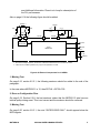
1
NOTE
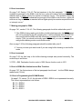
The default setting of bits 3 and 2 for option register 1 is determined by the settings of configuration pin.
19. Error in Table 6-14.
On page 6-77, The last column heading on Table 6-14 has an error. The heading should be:
“Number of clocks (DRAM)” not “Number of Wait States (DRAM)”
Section 7 – Communication Processor Module
1. Global advisory concerning Buffer Descriptor status bits.
The user is responsible for clearing (writing a zero) any buffer descriptor (RxBD or TxBD)
status bits set by the communication processor.
2. Deletion of STP bit.
On page 7-26, section 7.6.2.1. The STP bit in the ICCR was designed to conserve power
when IDMA was not in use. This function has been removed due to erratic behavior. The
user must keep this bit clear. Bit 15 of ICCR is now reserved.
3. Error in note.
On page 7-33, the note under section 7.6.3 Interface Signals should be as follows.
NOTE
DREQ must be level sensitive if IDMA uses buffer chaining or
auto buffer mode.
4. Wrong section number.
On page 7-34, the last sentence on the page "7.5.2.5 Timer Capture Register..." The section
was not correct. The correct section number is 7.6.2.5.
5. Wrong table reference.
On page 7-35, first sentence in section 7.6.4.2.1 reference, table 7-2. This should be table
7-3.
MOTOROLA
MC68360 USER’S MANUAL ERRATA
9