1
Mindi™
Amplifier Designer
User’s Guide
© 2009 Microchip Technology Inc.
DS51690B
Note the following details of the code protection feature on Microchip devices:
•
Microchip products meet the specification contained in their particular Microchip Data Sheet.
•
Microchip believes that its family of products is one of the most secure families of its kind on the market today, when used in the
intended manner and under normal conditions.
•
There are dishonest and possibly illegal methods used to breach the code protection feature. All of these methods, to our
knowledge, require using the Microchip products in a manner outside the operating specifications contained in Microchip’s Data
Sheets. Most likely, the person doing so is engaged in theft of intellectual property.
•
Microchip is willing to work with the customer who is concerned about the integrity of their code.
•
Neither Microchip nor any other semiconductor manufacturer can guarantee the security of their code. Code protection does not
mean that we are guaranteeing the product as “unbreakable.”
Code protection is constantly evolving. We at Microchip are committed to continuously improving the code protection features of our
products. Attempts to break Microchip’s code protection feature may be a violation of the Digital Millennium Copyright Act. If such acts
allow unauthorized access to your software or other copyrighted work, you may have a right to sue for relief under that Act.
Information contained in this publication regarding device
applications and the like is provided only for your convenience
and may be superseded by updates. It is your responsibility to
ensure that your application meets with your specifications.
MICROCHIP MAKES NO REPRESENTATIONS OR
WARRANTIES OF ANY KIND WHETHER EXPRESS OR
IMPLIED, WRITTEN OR ORAL, STATUTORY OR
OTHERWISE, RELATED TO THE INFORMATION,
INCLUDING BUT NOT LIMITED TO ITS CONDITION,
QUALITY, PERFORMANCE, MERCHANTABILITY OR
FITNESS FOR PURPOSE. Microchip disclaims all liability
arising from this information and its use. Use of Microchip
devices in life support and/or safety applications is entirely at
the buyer’s risk, and the buyer agrees to defend, indemnify and
hold harmless Microchip from any and all damages, claims,
suits, or expenses resulting from such use. No licenses are
conveyed, implicitly or otherwise, under any Microchip
intellectual property rights.
Trademarks
The Microchip name and logo, the Microchip logo, Accuron,
dsPIC, KEELOQ, KEELOQ logo, MPLAB, PIC, PICmicro,
PICSTART, rfPIC, SmartShunt and UNI/O are registered
trademarks of Microchip Technology Incorporated in the
U.S.A. and other countries.
FilterLab, Linear Active Thermistor, MXDEV, MXLAB,
SEEVAL, SmartSensor and The Embedded Control Solutions
Company are registered trademarks of Microchip Technology
Incorporated in the U.S.A.
Analog-for-the-Digital Age, Application Maestro, CodeGuard,
dsPICDEM, dsPICDEM.net, dsPICworks, dsSPEAK, ECAN,
ECONOMONITOR, FanSense, In-Circuit Serial
Programming, ICSP, ICEPIC, Mindi, MiWi, MPASM, MPLAB
Certified logo, MPLIB, MPLINK, mTouch, PICkit, PICDEM,
PICDEM.net, PICtail, PIC32 logo, PowerCal, PowerInfo,
PowerMate, PowerTool, REAL ICE, rfLAB, Select Mode, Total
Endurance, WiperLock and ZENA are trademarks of
Microchip Technology Incorporated in the U.S.A. and other
countries.
SQTP is a service mark of Microchip Technology Incorporated
in the U.S.A.
All other trademarks mentioned herein are property of their
respective companies.
© 2009, Microchip Technology Incorporated, Printed in the
U.S.A., All Rights Reserved.
Printed on recycled paper.
Microchip received ISO/TS-16949:2002 certification for its worldwide
headquarters, design and wafer fabrication facilities in Chandler and
Tempe, Arizona; Gresham, Oregon and design centers in California
and India. The Company’s quality system processes and procedures
are for its PIC® MCUs and dsPIC® DSCs, KEELOQ® code hopping
devices, Serial EEPROMs, microperipherals, nonvolatile memory and
analog products. In addition, Microchip’s quality system for the design
and manufacture of development systems is ISO 9001:2000 certified.
DS51690B-page ii
© 2009 Microchip Technology Inc.
MINDI™ AMPLIFIER DESIGNER
USER’S GUIDE
Table of Contents
Preface ........................................................................................................................... 1
Introduction............................................................................................................ 1
Document Layout .................................................................................................. 1
Conventions Used in this Guide ............................................................................ 2
Recommended Reading........................................................................................ 3
The Microchip Web Site ........................................................................................ 3
Customer Support ................................................................................................. 3
Document Revision History ................................................................................... 4
Chapter 1. Overview
1.1 Introduction ..................................................................................................... 5
1.2 Accessing Mindi™ .......................................................................................... 6
1.3 Amplifier Design ............................................................................................. 9
Chapter 2. Amplifier Circuit Design Tutorial
2.1 Introduction ................................................................................................... 13
2.2 Amplifier Design Example ............................................................................ 13
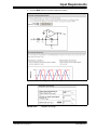
Chapter 3. Input Requirements
3.1 Introduction ................................................................................................... 23
3.2 Circuit Configuration ..................................................................................... 23
3.3 Description and Block Diagram .................................................................... 24
3.4 Power Supply ............................................................................................... 32
3.5 Load ............................................................................................................. 33
3.6 Amplifier Characteristics ............................................................................... 35
Chapter 4. Op Amp Selection
4.1 Introduction ................................................................................................... 39
4.2 Recommended Op Amps ............................................................................. 39
4.3 Op Amp Parameters ..................................................................................... 39
Chapter 5. Analyze
5.1 Introduction ................................................................................................... 41
5.2 Interactive Schematic ................................................................................... 41
5.3 Reset Design ................................................................................................ 61
5.4 Design Summary .......................................................................................... 62
5.5 Downloads, Samples and More ................................................................... 63
Worldwide Sales and Service .................................................................................... 64
© 2009 Microchip Technology Inc.
DS51690B-page iii
Mindi™ Amplifier Designer User’s Guide
NOTES:
DS51690B-page iv
© 2009 Microchip Technology Inc.
MINDI™ AMPLIFIER DESIGNER
USER’S GUIDE
Preface
NOTICE TO CUSTOMERS
All documentation becomes dated, and this manual is no exception. Microchip tools and
documentation are constantly evolving to meet customer needs, so some actual dialogs
and/or tool descriptions may differ from those in this document. Please refer to our web site
(www.microchip.com) to obtain the latest documentation available.
Documents are identified with a “DS” number. This number is located on the bottom of each
page, in front of the page number. The numbering convention for the DS number is
“DSXXXXXA”, where “XXXXX” is the document number and “A” is the revision level of the
document.
For the most up-to-date information on development tools, see the MPLAB® IDE on-line help.
Select the Help menu, and then Topics to open a list of available on-line help files.
INTRODUCTION
This chapter contains general information that will be useful to know before using the
Mindi™ Amplifier Designer & Simulator. Items discussed in this chapter include:
•
•
•
•
•
•
Document Layout
Conventions Used in this Guide
Recommended Reading
The Microchip Web Site
Customer Support
Document Revision History
DOCUMENT LAYOUT
This document describes how to use the Mindi™ Amplifier Designer & Simulator as a
development tool to emulate and debug firmware on a target board. The manual layout
is as follows:
• Chapter 1. “Overview” – this chapter provides an overview of the Mindi™
Amplifier Designer & Simulator.
• Chapter 2. “Amplifier Circuit Design Tutorial” – this chapter provides an
amplifier circuit design example.
• Chapter 3. “Input Requirements” – this chapter discusses the desired
parameters for the amplifier circuit.
• Chapter 4. “Op Amp Selection” – this chapter discusses the selection of op
amps to be used in the amplifier circuit design.
• Chapter 5. “Analyze” – this chapter discusses the analysis of the amplifier and
displays the amplifier circuit response.
© 2009 Microchip Technology Inc.
DS51690B-page 1
Mindi™ Amplifier Designer User’s Guide
CONVENTIONS USED IN THIS GUIDE
This manual uses the following documentation conventions:
DOCUMENTATION CONVENTIONS
Description
Arial font:
Italic characters
Represents
Referenced books
Emphasized text
A window
A dialog
A menu selection
A field name in a window or
dialog
A menu path
MPLAB® IDE User’s Guide
...is the only compiler...
the Output window
the Settings dialog
select Enable Programmer
“Save project before build”
A dialog button
A tab
A number in verilog format,
where N is the total number of
digits, R is the radix and n is a
digit.
A key on the keyboard
Click OK
Click the Power tab
4‘b0010, 2‘hF1
Italic Courier New
Sample source code
Filenames
File paths
Keywords
Command-line options
Bit values
Constants
A variable argument
Square brackets [ ]
Optional arguments
Curly brackets and pipe
character: { | }
Ellipses...
Choice of mutually exclusive
arguments; an OR selection
Replaces repeated text
#define START
autoexec.bat
c:\mcc18\h
_asm, _endasm, static
-Opa+, -Opa0, 1
0xFF, ‘A’
file.o, where file can be
any valid filename
mcc18 [options] file
[options]
errorlevel {0|1}
Initial caps
Quotes
Underlined, italic text with
right angle bracket
Bold characters
N‘Rnnnn
Text in angle brackets < >
Courier New font:
Plain Courier New
Represents code supplied by
user
DS51690B-page 2
Examples
File>Save
Press <Enter>, <F1>
var_name [,
var_name...]
void main (void)
{ ...
}
© 2009 Microchip Technology Inc.
Preface
RECOMMENDED READING
This user's guide describes how to use Mindi™ Amplifier Designer & Simulator. Other
useful documents are listed below. The following Microchip documents are available
and recommended as supplemental reference resources.
• AN 722, “Operational Amplifier DC Specifications and Applications”,
DS00722, Bonnie Baker, Microchip Technology Inc., 2000.
• AN 723, “Operational Amplifier AC Specifications and Applications”,
DS00723, Bonnie Baker, Microchip Technology Inc., 2000.
• AN 682, “Using Single Supply Operational Amplifiers in Embedded
Systems”, DS00682, Bonnie Baker, Microchip Technology Inc., 2000.
• AN 884, “Driving Capacitive Loads with Op Amps”, DS00884, Kumen Blake,
Microchip Technology Inc., 2003.
• AN 990, “Analog Sensor Conditioning Circuits - An Overview”, DS00990,
Kumen Blake, Microchip Technology Inc., 2005.
These application notes and others are listed in the design guide:
• “Signal Chain Design Guide”, DS21825.
THE MICROCHIP WEB SITE
Microchip provides online support via our web site at www.microchip.com. This web
site is used as a means to make files and information easily available to customers.
Accessible by using your favorite Internet browser, the web site contains the following
information:
• Product Support – Data sheets and errata, application notes and sample
programs, design resources, user’s guides and hardware support documents,
latest software releases and archived software
• General Technical Support – Frequently Asked Questions (FAQs), technical
support requests, online discussion groups, Microchip consultant program
member listing
• Business of Microchip – Product selector and ordering guides, latest Microchip
press releases, listing of seminars and events, listings of Microchip sales offices,
distributors and factory representatives
CUSTOMER SUPPORT
Users of Microchip products can receive assistance through several channels:
•
•
•
•
Distributor or Representative
Local Sales Office
Field Application Engineer (FAE)
Technical Support
Customers should contact their distributor, representative or field application engineer
(FAE) for support. Local sales offices are also available to help customers. A listing of
sales offices and locations is included in the back of this document.
Technical support is available through the web site at: http://support.microchip.com.
© 2009 Microchip Technology Inc.
DS51690B-page 3
Mindi™ Amplifier Designer User’s Guide
DOCUMENT REVISION HISTORY
Revision B (April 2009)
• Updated the Tool’s Name to Mindi™ Amplifier Designer & Simulator.
• Added Two Amplifier Circuits: Inverting Differentiator and Inverting Integrator.
Revision A (November 2007)
• Initial Release of this Document.
DS51690B-page 4
© 2009 Microchip Technology Inc.
MINDI™ AMPLIFIER DESIGNER
USER’S GUIDE
Chapter 1. Overview
1.1
INTRODUCTION
The Mindi™ Amplifier Designer & Simulator is an Application Circuit within the Mindi™
Circuit Designer & Simulator, which is available on the Microchip home page
(http://www.microchip.com) under “Analog Design & Sim. Tool” or going directly to
the Mindi home page (http://www.microchip.com/mindi). The Mindi™ Amplifier
Designer & Simulator generates full schematic diagrams of the amplifier circuit with
recommended component values and displays the signal responses in frequency and
time domains.
The Mindi™ Amplifier Designer & Simulator allows the following designs:
•
•
•
•
•
•
•
•
Inverting Amplifier
Non-inverting Amplifier
Voltage Follower
Difference Amplifier
Inverting Summing Amplifier
Inverting Comparator
Inverting Differentiator
Inverting Integrator
Once the amplifier characteristics have been identified, the Mindi™ Amplifier Designer
& Simulator can generate and simulate the schematic of the amplifier circuit. For
maximum design flexibility, changes in resistor and capacitor values can be
implemented to fit the demands of the application. The tool also generates a Design
Summary of the designed amplifier, including Design Requirements, Application
Schematic, Result Plot, and Bill of Materials (BOM). Users can directly download the
schematic, BOM, and Mindi™ offline version. The op amps and evaluation boards also
can be ordered from the Microchip web site at www.microchip.com.
© 2009 Microchip Technology Inc.
DS51690B-page 5
Mindi™ Amplifier Designer User’s Guide
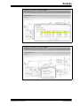
1.2
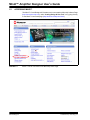
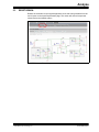
ACCESSING MINDI™
The Mindi™ Circuit Designer & Simulator can be accessed on Microchip’s Home Page
(http://www.microchip.com) under “Analog Design & Sim. Tool” or by going directly
to the Mindi™ Home web page (http://www.microchip.com/mindi).
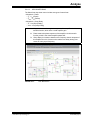
FIGURE 1-1:
DS51690B-page 6
Mindi™ can be accessed on the Microchip Home Page.
© 2009 Microchip Technology Inc.
Overview
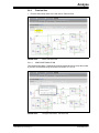
The Mindi™ Home Page is shown in Figure 1-2. To enter the Mindi™ Circuit Designer
& Simulator, click the Click Here to Start button in the window.
FIGURE 1-2:
Home Page.
Bring up the Mindi™ Circuit Designer & Simulator on the Mindi™
Once users log onto Mindi™, the Mindi™ home page is displayed, (as shown in
Figure 1-3) indicating the application circuits that are available for design and simulation. The Amplifiers button is located in the upper-left corner of the web page. Click
on it to enter the amplifier online design and simulation test environment.
The first time Amplifiers is accessed, users will be prompted to provide some basic
registration information, as shown in Figure 1-4. Once registered, an account is created
on the Host Server and users will be able to generate and analyze designs on the
Mindi™ Circuit Designer & Simulator web page. Custom designs can also be saved to
users’ PC, where they can be accessed for future reference.
Note:
© 2009 Microchip Technology Inc.
If a Pop-Up Blocker is enabled on the users’ browser, there may be a
problem with the registration process. Please be sure to disable this feature
when registering on Mindi™. On Internet Explorer, this is done by selecting
the Pop-Up Blocker window under the Tools pull-down menu.
DS51690B-page 7
Mindi™ Amplifier Designer User’s Guide
FIGURE 1-3:
Application Circuit.
FIGURE 1-4:
New User Registration.
DS51690B-page 8
© 2009 Microchip Technology Inc.
Overview
1.3
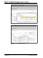
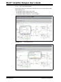
AMPLIFIER DESIGN
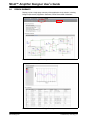
The Mindi™ Amplifier Designer & Simulator has four amplifier design tabs which
include Application Circuit, Input Requirements, Op Amp Selection, and Analyze,
as shown on the Tab bar on the top of the tool page in Figure 1-5. These tabs allow the
user to move through the design steps of specifying performance requirements. An
overview of the Mindi™ Amplifier Designer & Simulator is given in the following
sections.
1.3.1
Application Circuit Tab
The amplifier circuit design starts from the Application Circuit tab (see Figure 1-3).
Select the Amplifiers button to enter the online simulation test environment.
1.3.2
Input Requirements Tab
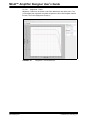
Click the Input Requirements tab and set desired parameters for the amplifier circuit.
(This tab is discussed in more detail in Chapter 3. “Input Requirements”.)
FIGURE 1-5:
Input Requirements.
© 2009 Microchip Technology Inc.
DS51690B-page 9
Mindi™ Amplifier Designer User’s Guide
1.3.3
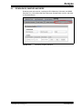
Op Amp Selection Tab
Click the Op Amp Selection tab, choose an op amp to be used in the amplifier circuit
and click the corresponding Analyze link to start the next phase of the design. (This tab
is discussed in more detail in Chapter 4. “Op Amp Selection”).
FIGURE 1-6:
DS51690B-page 10
Op Amp Selection.
© 2009 Microchip Technology Inc.
Overview
1.3.4
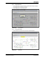
Analyze Tab
There are four buttons associated with the Analyze tab:
•
•
•
•
Interactive Schematic
Reset Design
Design Summary
Downloads, Samples and More
The Mindi™ Amplifier Designer & Simulator generates the amplifier circuit schematic
on this tab. For maximum design flexibility, changes in resistor and capacitor values
can be implemented to fit the demands of the application. To run a simulation, choose
a mode from the Select drop-down menu and click the Run button to simulate the
schematic. Once the simulation is complete, waveforms will be available via the
Waveforms drop-down menu. A single-page design summary can be generated by
clicking Design Summary button. Moreover, the schematic, amplifier SPICE model
and Mindi™ offline version can be downloaded. (This tab is discussed in more detail in
Chapter 5. “Analyze”).
FIGURE 1-7:
Analyze.
© 2009 Microchip Technology Inc.
DS51690B-page 11
Mindi™ Amplifier Designer User’s Guide
NOTES:
DS51690B-page 12
© 2009 Microchip Technology Inc.
MINDI™ AMPLIFIER DESIGNER
USER’S GUIDE
Chapter 2. Amplifier Circuit Design Tutorial
2.1
INTRODUCTION
This chapter steps users through the design of an example amplifier circuit.
2.2
AMPLIFIER DESIGN EXAMPLE
Design a non-inverting amplifier with the following requirements:
•
•
•
•
Closed Loop Gain = +2 V/V
Power Supply Voltage = 5.0V
Load Type: Resistor-Capacitor
Load Capacitance = 60 pF
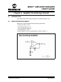
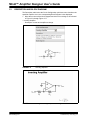
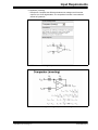
The block diagram of a non-inverting amplifier is shown in Figure 2-1.
FIGURE 2-1:
© 2009 Microchip Technology Inc.
Block Diagram for a Non-Inverting Amplifier.
DS51690B-page 13
Mindi™ Amplifier Designer User’s Guide
1. To access the Mindi™ Amplifier Designer & Simulator, refer to
Section 1.2 “Accessing Mindi™” for more detail (especially Figure 1-3).
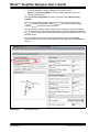
2. Set Desired Parameters
Click the Circuit Configuration drop-down menu and choose Non-Inverting
Amplifier.
The Power Supply dialog enables users to specify the minimum power supply
(VDD-min), nominal power supply voltage (VDD-nom), and maximum power supply
voltage (VDD-max). Enter 5.0 in these text boxes.
The Non-Inverting Amplifier dialog enables users to specify the desired closed loop
gain (G), Peak-to-Peak Output Signal Voltage (GVPP), and Max Input Signal Frequency
(Fin-max). Enter 2 in the text box of desired closed loop gain. Use default values for the
other text boxes.
The Load dialog enables users to specify the load type. Click the Load Type
drop-down menu and choose Resistor-Capacitor. Enter 60p in the Load Capacitance
text box.
FIGURE 2-2:
DS51690B-page 14
Input Requirements.
© 2009 Microchip Technology Inc.
Amplifier Circuit Design Tutorial
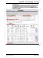
3. Select Op Amp
The Non-Inverting Amplifier table lists key amplifier design information as a reminder.
The Recommended Op Amps table lists those op amps that come close to the
recommended op amp specifications. For this tutorial, select MCP6021 by clicking the
corresponding Analyze link.
FIGURE 2-3:
Op Amp Selection.
© 2009 Microchip Technology Inc.
DS51690B-page 15
Mindi™ Amplifier Designer User’s Guide
4. Analyze
The Mindi™ Amplifier Designer & Simulator automatically generates the full schematic
diagram of the amplifier circuit with recommended component values. There are three
types of analysis in the Select drop-down menu: Transient Step, Transient Sine, and
AC Analysis.
First, choose AC Analysis. Then, click the Configure button to set up the AC
simulation condition. This pull-down menu allows the user to set up the start frequency,
stop frequency, and resolution. Finally, click the Run button to simulate the schematic.
Once the simulation is completed, the AC response will be available via the Waveforms
drop-down menu. Similarly, the Transient Step and the Sine Analysis can be completed
and the transient responses will also be available via the Waveforms drop-down menu.
Moreover, a design summary can be generated by clicking the Design Summmary
button (see Figures 2-4 to Figure 2-14).
FIGURE 2-4:
DS51690B-page 16
AC Analysis.
© 2009 Microchip Technology Inc.
Amplifier Circuit Design Tutorial
FIGURE 2-5:
Configure the Simulation.
FIGURE 2-6:
Running the Simulation.
© 2009 Microchip Technology Inc.
DS51690B-page 17
Mindi™ Amplifier Designer User’s Guide
DS51690B-page 18
FIGURE 2-7:
Simulation Complete.
FIGURE 2-8:
View the Waveform.
© 2009 Microchip Technology Inc.
Amplifier Circuit Design Tutorial
FIGURE 2-9:
AC Response: Magnitude-Phase.
FIGURE 2-10:
AC Response: Magnitude-Group Delay.
© 2009 Microchip Technology Inc.
DS51690B-page 19
Mindi™ Amplifier Designer User’s Guide
DS51690B-page 20
FIGURE 2-11:
Transient Sine Response.
FIGURE 2-12:
Transient Step Response.
© 2009 Microchip Technology Inc.
Amplifier Circuit Design Tutorial
FIGURE 2-13:
Design Summary.
FIGURE 2-14:
© 2009 Microchip Technology Inc.
Downloads, Samples and More.
DS51690B-page 21
Mindi™ Amplifier Designer User’s Guide
NOTES:
DS51690B-page 22
© 2009 Microchip Technology Inc.
MINDI™ AMPLIFIER DESIGNER
USER’S GUIDE
Chapter 3. Input Requirements
3.1
INTRODUCTION
This chapter discusses the Mindi™ Input Requirements tab in greater detail. The
Input Requirements tab is shown in Figure 1-5 in Section 1.3.2.
3.2
CIRCUIT CONFIGURATION
The Circuit Configuration drop-down menu enables the user to specify the amplifier
circuit type as: Inverting Amplifier, Non-Inverting Amplifier, Voltage Follower, Difference
Amplifier, Inverting Summing Amplifier, Inverting Comparator, Inverting Differentiator
and Inverting Integrator.
FIGURE 3-1:
© 2009 Microchip Technology Inc.
Circuit Configuration.
DS51690B-page 23
Mindi™ Amplifier Designer User’s Guide
3.3
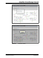
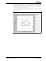
DESCRIPTION AND BLOCK DIAGRAM
The Description table below the Circuit Configuration pull-down menu describes the
specified amplifier circuit; the corresponding Block Diagram is also displayed.
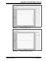
1. Move the mouse over the block diagram and click on it to enlarge it, as indicated
in Figure 3-2 through Figure 3-17.
• Inverting Amplifier
- Description: Inverts and amplifies a voltage.
DS51690B-page 24
FIGURE 3-2:
Inverting Amplifier.
FIGURE 3-3:
Enlarged Inverting Amplifier Block Diagram.
© 2009 Microchip Technology Inc.
Input Requirements
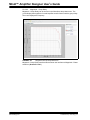
• Non-Inverting Amplifier
- Description: Amplifies a voltage with a gain > +1 V/V.
FIGURE 3-4:
Non-Inverting Amplifier.
FIGURE 3-5:
Enlarged Non-Inverting Amplifier Block Diagram.
© 2009 Microchip Technology Inc.
DS51690B-page 25
Mindi™ Amplifier Designer User’s Guide
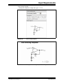
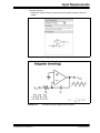
• Voltage Follower
- Description: Known as a Unity Gain Buffer and as a Voltage Follower.
Amplifies a voltage with a gain of +1 V/V.
DS51690B-page 26
FIGURE 3-6:
Voltage Follower.
FIGURE 3-7:
Enlarged Voltage Follower Block Diagram.
© 2009 Microchip Technology Inc.
Input Requirements
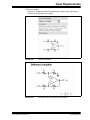
• Difference Amplifier
- Description: Amplifies the difference between two voltages, while rejecting the
common mode (average) input voltage.
FIGURE 3-8:
Difference Amplifier.
FIGURE 3-9:
Enlarged Difference Amplifier Block Diagram.
© 2009 Microchip Technology Inc.
DS51690B-page 27
Mindi™ Amplifier Designer User’s Guide
• Summing Amplifier (Inverting)
- Description: Amplifies two or more input voltages with an inverting gain.
DS51690B-page 28
FIGURE 3-10:
Inverting Summing Amplifier.
FIGURE 3-11:
Enlarged Inverting Summing Amplifier Block Diagram.
© 2009 Microchip Technology Inc.
Input Requirements
• Comparator (Inverting)
- Description: Compares the difference between two voltages and forces the
output to one of two digital states. The comparison includes a user selected
amount of hysteresis.
FIGURE 3-12:
Inverting Comparator.
FIGURE 3-13:
Enlarged Inverting Comparator Block Diagram.
© 2009 Microchip Technology Inc.
DS51690B-page 29
Mindi™ Amplifier Designer User’s Guide
• Inverting Differentiator
- Description: Output voltage is proportional to the negative derivative of the
input voltage.
DS51690B-page 30
FIGURE 3-14:
Inverting Differentiator.
FIGURE 3-15:
Enlarged Inverting Differentiator Block Diagram.
© 2009 Microchip Technology Inc.
Input Requirements
• Inverting Integrator
- Description: Output voltage is proportional to the negative integral of the input
voltage.
FIGURE 3-16:
Inverting Integrator.
FIGURE 3-17:
Enlarged Inverting Integrator Block Diagram.
© 2009 Microchip Technology Inc.
DS51690B-page 31
Mindi™ Amplifier Designer User’s Guide
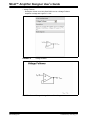
3.4
POWER SUPPLY
The ”Power Supply” text boxes allow users to modify the power supply requirement of
the amplifier circuit. The allowable range of power supply is 1.4V to 5.5V.
1. Move the mouse over the text and view the ranges, as indicated in Figure 3-18
through Figure 3-21.
DS51690B-page 32
FIGURE 3-18:
Power Supply Text Boxes.
FIGURE 3-19:
Nominal Power Supply Voltage.
FIGURE 3-20:
Minimum Power Supply Voltage.
FIGURE 3-21:
Maximum Power Supply Voltage.
© 2009 Microchip Technology Inc.
Input Requirements
3.5
LOAD
The Load Type drop-down menu specifies six load types: Resistor-Capacitor, ADC,
PIC, Coax, Twisted Pair, and Ribbon Cable. The corresponding characteristics text
boxes allow users to modify the load parameters, as indicated in Figure 3-18 through
Figure 3-21.
3.5.1
Resistor-Capacitor
The allowable range of Load Capacitance is 0F to 1 µF.
1. Move the mouse over the text and the range will be shown.
.
FIGURE 3-22:
3.5.2
Load Type: Resistor-Capacitor.
ADC, PIC
The allowable range of Load Capacitance is 0F to 1 µF. The allowable range of Load
Resistance is 100Ω to 10 MΩ.
1. Move the mouse over the text and the range will be shown.
.
FIGURE 3-23:
Load Type: ADC.
FIGURE 3-24:
Load Type: PIC.
© 2009 Microchip Technology Inc.
DS51690B-page 33
Mindi™ Amplifier Designer User’s Guide
3.5.3
Coax, Twisted Pair, and Ribbon Cable
The allowable range of Length is 10 mm to 1 km. The allowable range of Capacitance
per Length is 1 pF/m to 1 nF/m.
1. Move the mouse over the text and the range will be shown.
.
DS51690B-page 34
FIGURE 3-25:
Load Type: Coax.
FIGURE 3-26:
Load Type: Twisted Pair.
FIGURE 3-27:
Load Type: Ribbon Cable.
© 2009 Microchip Technology Inc.
Input Requirements
3.6
AMPLIFIER CHARACTERISTICS
The Amplifier Characteristics text boxes allow users to specify the Desired Closed
Loop Gain, Peak-to-Peak Output Signal Voltage, Maximum Input Signal Frequency,
etc, as shown in Figure 3-28 through Figure 3-37.
1. The allowable range of Desired Closed Loop Gain is 0.1 V/V to 10 kV/V.
2. The allowable range of Peak-to-Peak Output Signal Voltage is 1 mVpp to 5.5 Vpp.
Note:
The Mindi™ Amplifier Designer & Simulator will automatically calculate the
Peak-to-Peak Input Signal Voltage according to the Peak-to-Peak Output
Signal Voltage specified by users.
3. The allowable range of Max Input Signal Frequency is 1 Hz to 1 MHz.
FIGURE 3-28:
Inverting Amplifier.
FIGURE 3-29:
Non-Inverting Amplifier.
FIGURE 3-30:
Voltage Follower.
© 2009 Microchip Technology Inc.
DS51690B-page 35
Mindi™ Amplifier Designer User’s Guide
DS51690B-page 36
FIGURE 3-31:
Difference Amplifier.
FIGURE 3-32:
Summing Amplifier (Inverting).
FIGURE 3-33:
Comparator (Inverting).
FIGURE 3-34:
Differentiator (Inverting).
© 2009 Microchip Technology Inc.
Input Requirements
4. Click the INFO button to view the advanced summary.
FIGURE 3-35:
Viewing Advanced Summary.
FIGURE 3-36:
Integrator (Inverting).
© 2009 Microchip Technology Inc.
DS51690B-page 37
Mindi™ Amplifier Designer User’s Guide
5. Click INFO button to view the advanced summary.
FIGURE 3-37:
Viewing Advanced Summary.
6. After setting the desired specifications for the input requirments, click the Op
Amp Selection tab to select the op amp to be used in this amplifier.
DS51690B-page 38
© 2009 Microchip Technology Inc.
MINDI™ AMPLIFIER DESIGNER
USER’S GUIDE
Chapter 4. Op Amp Selection
4.1
INTRODUCTION
This chapter discusses the Mindi Op Amp Selection tab in greater detail. The Op Amp
Selection tab is shown in Figure 1-6 in Section 1.3.4. This tab allows the user to
specify which Microchip op amp is used in the amplifier circuit.
4.2
RECOMMENDED OP AMPS
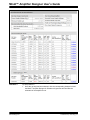
Four table are provided in this tab as indicated in Figure 4-1.
1. The Amplifier Characteristics table lists the key amplifier design information as a
reference.
2. The Op Amp Design Constraints and Recommended Op Amp Parameters tables
show the recommended op amp specifications for the amplifier design.
3. The Recommended Op Amps table lists those op amps that come close to the
recommended op amp specifications. The ideal op amp list at the top is included
for comparing simulation results to textbook amplifier responses.
4. The Other Op Amps table lists other op amps that are not as close to the
recommended op amp specifications. Click the Show button to display these op
amps; the op amps and parameters that do not meet recommendations are
indicated in red.
4.3
OP AMP PARAMETERS
The following parameters and their definitions will help the designer choose the correct
op amp.
1. Gain Bandwidth Product:
The product of op amp open-loop gain times the frequency at any point where
the amplifier response is attenuating at a rate of -20 dB/decade of frequency.
2. Slew Rate:
The maximum rate of change at the output of an op amp. Basically, it shows how
fast the output can “follow” the input.
3. Minimum Stable Gain:
The minimum gain at which an op amp can be set while still remaining stable.
Most op amps are unity gain stable (G ≥ +1 V/V). A few op amps need to be set
at higher gains to remain stable (e.g., G ≥ +10 V/V for the MCP6141).
4. Power Supply Voltage:
The acceptable supply voltage that allows the linear operation of an op amp.
5. Quiescent Current (Iq):
The amount of current consumed by the op amp when it is not performing any
work (idle).
6. Rail-to-Rail Input/Output:
The op amp will operate correctly when its input/output is closely driven to either
power rail under defined operating conditions. (N means No and Y means Yes).
© 2009 Microchip Technology Inc.
DS51690B-page 39
Mindi™ Amplifier Designer User’s Guide
FIGURE 4-1:
Op Amp Selection.
1. Once the op amp has been selected, click the corresponding Analyze link and
the Mindi™ Amplifier Designer & Simulator will generate and simulate the
schematic of the amplifier circuit.
DS51690B-page 40
© 2009 Microchip Technology Inc.
MINDI™ AMPLIFIER DESIGNER
USER’S GUIDE
Chapter 5. Analyze
5.1
INTRODUCTION
This chapter discusses the Mindi Analyze tab in greater detail. The Analyze tab is
shown in Figure 1-7 in Section 1.3.4. This tab includes four buttons which selects the
following views: Interactive Schematic, Reset Design, Design Summary and
Downloads, Samples and More.
5.2
INTERACTIVE SCHEMATIC
5.2.1
Schematic Viewer
The Mindi™ Amplifier Designer & Simulator automatically generates the full schematic
view of the amplifier circuit with recommended component values based on the Input
Requirements. Various simulation operations can also be selected in order to analyze
and evaluate the performance of the amplifier circuit. In addition, the individual
components of the schematic can be modified, allowing users to further evaluate the
design solution. Detailed help on using the Schematic Viewer can be accessed via the
Help button.
FIGURE 5-1:
© 2009 Microchip Technology Inc.
Schematic Viewer.
DS51690B-page 41
Mindi™ Amplifier Designer User’s Guide
5.2.2
Edit Component Value
The value of a component (resistor or capacitor) can be changed from its default value
calculated by the Mindi™ Amplifier Designer & Simulator. Changing the component
value only affects the component that is selected. To adjust a component value, click
on the component to access its attributes window, as shown in Figure 5-2 through
Figure 5-5.
• Database Tab: Contains recommended parts to use with this circuit. Users can
click on the header of any column to sort the database by that column. Column
widths can also be adjusted by dragging the boundary between columns.
• Custom Tab: Enter custom parameter for this component.
The allowable range of capacitance is from 1.0 pF to 10 µF.
The allowable range of resistance is from 0Ω to 1.0 GΩ.
Note 1:
0Ω , 1.0 GΩ, 1.0 pF, and 10 µF are intended for simulation purposes and
are not practical in real applications.
2:
To remove parts from the schematic for simulation purposes, use 1.0 GΩ
for shunt resistors, 0Ω for series resistor, use 1.0 pF for shunt capacitors
and 10 µF for series capacitors.
.
Note:
DS51690B-page 42
It is the user’s responsibility to ensure the proper circuit behavior when the
component values are changed.
© 2009 Microchip Technology Inc.
Analyze
FIGURE 5-2:
Edit Capacitor: Database Tab.
FIGURE 5-3:
Edit Capacitor: Custom Tab.
© 2009 Microchip Technology Inc.
DS51690B-page 43
Mindi™ Amplifier Designer User’s Guide
DS51690B-page 44
FIGURE 5-4:
Edit Resistor: Database Tab.
FIGURE 5-5:
Edit Resistor: Custom Tab.
© 2009 Microchip Technology Inc.
Analyze
5.2.3
Edit Op Amp
The type of op amp can also be changed. Changing the type of op amp only affects the
op amp that is selected as shown in Figure 5-6.
1. To change the op amp, move the mouse over the appropriate op amp, then
left-click the mouse. The attributes window will appear. Select the type of op amp
and click OK.
Note:
It is the user’s responsibility to ensure the proper circuit behavior when the
op amp is changed.
FIGURE 5-6:
© 2009 Microchip Technology Inc.
Edit Op Amp.
DS51690B-page 45
Mindi™ Amplifier Designer User’s Guide
5.2.4
Select Analysis
Three types of analysis may be selected in the Select drop-down menu: Transient Step,
Transient Sine, and AC Analysis.
• Transient Analysis or time-domain analysis most closely simulates the
phenomena seen in the real circuit by means of an oscilloscope. A simulation
consists usually of a time sweep starting at t = 0. There are two types of Transient
Analysis: Transient Step and Transient Sine
• AC Analysis or frequency-domain analysis is used mainly in connection with
amplifiers when the frequency response is needed. The AC simulation is usually
based on a sweep over a range of frequencies. In the real world, this kind of
measurement would be made with a network analyzer (the source power would
be small enough to not excite any non-linearities, such as slew rate)
5.2.4.1
AC ANALYSIS
AC Analysis can be chosen from the Select drop-down menu.
FIGURE 5-7:
DS51690B-page 46
Select AC Analysis.
© 2009 Microchip Technology Inc.
Analyze
5.2.4.2
CONFIGURE SIMULATION
The “Configure Simulation: AC Analysis” text boxes allow users to set up the start
frequency and the stop frequency.
• The allowable range of start and stop frequencies: 0.001 Hz to 1 GHz.
FIGURE 5-8:
© 2009 Microchip Technology Inc.
Configure Simulation: AC Analysis.
DS51690B-page 47
Mindi™ Amplifier Designer User’s Guide
5.2.4.3
RUN SIMULATION
1. Click the Run button to start the simulation. The Simulation Complete message
box appears when the simulation is complete.
2. Click the OK button to view the waveforms. (See Figure 5-9 and Figure 5-10).
DS51690B-page 48
FIGURE 5-9:
Run Simulation.
FIGURE 5-10:
Simulation Complete.
© 2009 Microchip Technology Inc.
Analyze
5.2.4.4
VIEW WAVEFORMS
The Waveforms drop-down menu includes two types of waveforms:
• Magnitude - Phase
- VL - VIN (Phase)
- VOUT - VIN (Phase)
• Magnitude - Group Delay
- VL - VIN (Group Delay)
- VOUT - VIN (Group Delay)
Note 1:
Magnitude means the magnitude response of the amplifier circuit's
transfer function, which is the overall amplifier gain.
2:
Phase means the phase response of the amplifier circuit's transfer
function, which is the overall amplifier phase shift.
3:
Group Delay is a measure based on the frequency domain response of
the amplifier circuit. It focuses on the relative time delay among sine
waves of nearly equal frequency.
FIGURE 5-11:
© 2009 Microchip Technology Inc.
View Waveforms.
DS51690B-page 49
Mindi™ Amplifier Designer User’s Guide
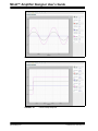
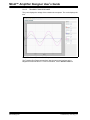
5.2.4.4.1
Magnitude - Phase
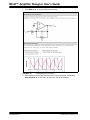
Magnitude - Phase can be chosen in the View Waveforms drop-down menu. The
y-axes display the magnitude and phase responses of the overall amplifier transfer
function. The x-axis displays the frequency.
FIGURE 5-12:
DS51690B-page 50
Magnitude - Phase Waveform.
© 2009 Microchip Technology Inc.
Analyze
M1 or M2 can be moved horizontally to a desired frequency value. Or, double click M1
or M2 and a dialog box will appear; you can input a frequency value to force the marker
to that value. (See Figure 5-13). After the frequency value are set for M1 and M2, the
values of magnitude and phase will be updated.
Also worth noting are the buttons in the upper left hand corner of the window (Zoom In,
Zoom Out, Magnifier, Hand Tool, Reset View, and Print) that allow the waveform view
to be changed or printed.
FIGURE 5-13:
© 2009 Microchip Technology Inc.
Set Value for Markers.
DS51690B-page 51
Mindi™ Amplifier Designer User’s Guide
5.2.4.4.2
Magnitude - Group Delay
Magnitude - Group Delay can be chosen in the Waveforms drop-down menu. The
y-axes display the magnitude of overall amplifier transfer function and the group delay.
The x-axis displays the frequency.
FIGURE 5-14:
Magnitude-Group Delay Waveform.
Magnitude - Group Delay waveform has the same user interface as Magnitude - Phase
waveform (Section 5.2.4.4.1).
DS51690B-page 52
© 2009 Microchip Technology Inc.
Analyze
5.2.5
Transient Step
Transient Step can be chosen from the Select drop-down menu.
.
FIGURE 5-15:
5.2.5.1
Select Transient Step.
CONFIGURE SIMULATION
The Configure Simulation: Transient Step text boxes allow the user to set up the
stop time, or duration of the step response. The allowable range of Stop Time: 1 µs to
1s.
FIGURE 5-16:
© 2009 Microchip Technology Inc.
Configure Simulation: Transient Step.
DS51690B-page 53
Mindi™ Amplifier Designer User’s Guide
5.2.5.2
EDIT VOLTAGE SOURCE
The Configure Source text boxes allow the user to set up the Center, Step Amplitude,
and Delay of VIN.
• The allowable range of Center: 0V to 5.5V
• The allowable range of Step Amplitude: 0V to 10V
• The allowable range of Delay: 1 µs to 1s
FIGURE 5-17:
DS51690B-page 54
Edit Voltage Source.
© 2009 Microchip Technology Inc.
Analyze
5.2.5.3
RUN SIMULATION
1. Click the Run button to start the simulation. The Simulation Complete message
box appears when the simulation is complete. Click the OK button to view the
waveforms.
FIGURE 5-18:
Run Simulation.
FIGURE 5-19:
Simulation Complete.
© 2009 Microchip Technology Inc.
DS51690B-page 55
Mindi™ Amplifier Designer User’s Guide
5.2.5.4
VIEW WAVEFORMS
1. Click the Waveform drop-down menu and select Transient Response.
FIGURE 5-20:
5.2.5.5
Waveforms.
TRANSIENT STEP RESPONSE
The y-axis displays the voltage of the transient step response. The x-axis displays the
time.
FIGURE 5-21:
Transient Step Response.
Transient Step Response waveform has the same user interface as Magnitude-Phase
waveform. For more information, refer to Section 5.2.4.4.1.
DS51690B-page 56
© 2009 Microchip Technology Inc.
Analyze
5.2.6
Transient Sine
1. Click the Select drop-down menu and choose Transient Sine.
.
FIGURE 5-22:
5.2.6.1
Select Transient Sine.
CONFIGURE SIMULATION
The Configure Simulation: Transient Sine text box allows the user to set up the number
of periods. The allowable range of Number of Periods: 0.5T to 10T.
FIGURE 5-23:
© 2009 Microchip Technology Inc.
Configure Simulation: Transient Sine.
DS51690B-page 57
Mindi™ Amplifier Designer User’s Guide
5.2.6.2
EDIT VOLTAGE SOURCE
The Configure Source text boxes allow the user to set up the Center, Peak-to-Peak,
and Frequency of VIN.
• The allowable range of Center: 0V to 5.5V
• The allowable range of Peak-to-Peak: 0V to 10V
• The allowable range of Frequency: 1 Hz to 100 MHz
DS51690B-page 58
FIGURE 5-24:
Edit Voltage Source.
FIGURE 5-25:
Simulation Complete.
© 2009 Microchip Technology Inc.
Analyze
5.2.6.3
RUN SIMULATION
1. Click the Run button to start the simulation. The Simulation Complete message
box appears when the simulation is complete.
2. Click the OK button to view the waveforms.
FIGURE 5-26:
5.2.6.4
Run Simulation.
VIEW WAVEFORMS
1. Click the Waveform drop-down menu and select Transient Response.
FIGURE 5-27:
© 2009 Microchip Technology Inc.
Waveforms.
DS51690B-page 59
Mindi™ Amplifier Designer User’s Guide
5.2.6.5
TRANSIENT SINE RESPONSE
The y-axis displays the voltage of the transient sine response. The x-axis displays the
time.
.
FIGURE 5-28:
Transient Sine Response.
The Transient Sine Response waveform has the same user interface as the
Magnitude-Phase waveform. For more information, refer to Section 5.2.4.4.1.
DS51690B-page 60
© 2009 Microchip Technology Inc.
Analyze
5.3
RESET DESIGN
Restore the schematic to the original application circuit that was generated from the
user’s inputs on the Input Requirements page. This action will reset all component
values back to their default values.
FIGURE 5-29:
© 2009 Microchip Technology Inc.
Reset Design.
DS51690B-page 61
Mindi™ Amplifier Designer User’s Guide
5.4
DESIGN SUMMARY
Display or print a single page summary of the application circuit solution, including
Design Requirements, Application Shematic, Result Plot and Bill of Materials.
DS51690B-page 62
FIGURE 5-30:
Design Summary.
FIGURE 5-31:
Continued Design Summary.
© 2009 Microchip Technology Inc.
Analyze
5.5
DOWNLOADS, SAMPLES AND MORE
Download tools and materials, including the Bill of Materials, Schematic, and MINDI
Simulator Tool. Link to Microchip Direct web page, Sample/Order a device, and Order
an Evaluation Board.
FIGURE 5-32:
© 2009 Microchip Technology Inc.
Download, Samples and More.
DS51690B-page 63
WORLDWIDE SALES AND SERVICE
AMERICAS
ASIA/PACIFIC
ASIA/PACIFIC
EUROPE
Corporate Office
2355 West Chandler Blvd.
Chandler, AZ 85224-6199
Tel: 480-792-7200
Fax: 480-792-7277
Technical Support:
http://support.microchip.com
Web Address:
www.microchip.com
Asia Pacific Office
Suites 3707-14, 37th Floor
Tower 6, The Gateway
Harbour City, Kowloon
Hong Kong
Tel: 852-2401-1200
Fax: 852-2401-3431
India - Bangalore
Tel: 91-80-3090-4444
Fax: 91-80-3090-4080
India - New Delhi
Tel: 91-11-4160-8631
Fax: 91-11-4160-8632
Austria - Wels
Tel: 43-7242-2244-39
Fax: 43-7242-2244-393
Denmark - Copenhagen
Tel: 45-4450-2828
Fax: 45-4485-2829
India - Pune
Tel: 91-20-2566-1512
Fax: 91-20-2566-1513
France - Paris
Tel: 33-1-69-53-63-20
Fax: 33-1-69-30-90-79
Japan - Yokohama
Tel: 81-45-471- 6166
Fax: 81-45-471-6122
Germany - Munich
Tel: 49-89-627-144-0
Fax: 49-89-627-144-44
Atlanta
Duluth, GA
Tel: 678-957-9614
Fax: 678-957-1455
Boston
Westborough, MA
Tel: 774-760-0087
Fax: 774-760-0088
Chicago
Itasca, IL
Tel: 630-285-0071
Fax: 630-285-0075
Cleveland
Independence, OH
Tel: 216-447-0464
Fax: 216-447-0643
Dallas
Addison, TX
Tel: 972-818-7423
Fax: 972-818-2924
Detroit
Farmington Hills, MI
Tel: 248-538-2250
Fax: 248-538-2260
Kokomo
Kokomo, IN
Tel: 765-864-8360
Fax: 765-864-8387
Los Angeles
Mission Viejo, CA
Tel: 949-462-9523
Fax: 949-462-9608
Santa Clara
Santa Clara, CA
Tel: 408-961-6444
Fax: 408-961-6445
Toronto
Mississauga, Ontario,
Canada
Tel: 905-673-0699
Fax: 905-673-6509
Australia - Sydney
Tel: 61-2-9868-6733
Fax: 61-2-9868-6755
China - Beijing
Tel: 86-10-8528-2100
Fax: 86-10-8528-2104
China - Chengdu
Tel: 86-28-8665-5511
Fax: 86-28-8665-7889
Korea - Daegu
Tel: 82-53-744-4301
Fax: 82-53-744-4302
China - Hong Kong SAR
Tel: 852-2401-1200
Fax: 852-2401-3431
Korea - Seoul
Tel: 82-2-554-7200
Fax: 82-2-558-5932 or
82-2-558-5934
China - Nanjing
Tel: 86-25-8473-2460
Fax: 86-25-8473-2470
Malaysia - Kuala Lumpur
Tel: 60-3-6201-9857
Fax: 60-3-6201-9859
China - Qingdao
Tel: 86-532-8502-7355
Fax: 86-532-8502-7205
Malaysia - Penang
Tel: 60-4-227-8870
Fax: 60-4-227-4068
China - Shanghai
Tel: 86-21-5407-5533
Fax: 86-21-5407-5066
Philippines - Manila
Tel: 63-2-634-9065
Fax: 63-2-634-9069
China - Shenyang
Tel: 86-24-2334-2829
Fax: 86-24-2334-2393
Singapore
Tel: 65-6334-8870
Fax: 65-6334-8850
China - Shenzhen
Tel: 86-755-8203-2660
Fax: 86-755-8203-1760
Taiwan - Hsin Chu
Tel: 886-3-6578-300
Fax: 886-3-6578-370
China - Wuhan
Tel: 86-27-5980-5300
Fax: 86-27-5980-5118
Taiwan - Kaohsiung
Tel: 886-7-536-4818
Fax: 886-7-536-4803
China - Xiamen
Tel: 86-592-2388138
Fax: 86-592-2388130
Taiwan - Taipei
Tel: 886-2-2500-6610
Fax: 886-2-2508-0102
China - Xian
Tel: 86-29-8833-7252
Fax: 86-29-8833-7256
Thailand - Bangkok
Tel: 66-2-694-1351
Fax: 66-2-694-1350
Italy - Milan
Tel: 39-0331-742611
Fax: 39-0331-466781
Netherlands - Drunen
Tel: 31-416-690399
Fax: 31-416-690340
Spain - Madrid
Tel: 34-91-708-08-90
Fax: 34-91-708-08-91
UK - Wokingham
Tel: 44-118-921-5869
Fax: 44-118-921-5820
China - Zhuhai
Tel: 86-756-3210040
Fax: 86-756-3210049
03/26/09
DS51690B-page 64
© 2009 Microchip Technology Inc.