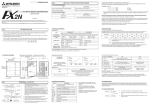
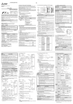
1
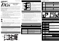
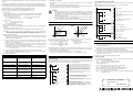
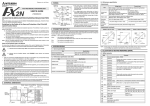
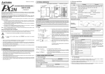
5.3 Performance specification
3. WIRING
Analog Inputs
1
Shielded
This manual should be used by trained and competent personnel. The definition of such a person or
persons is as follows:
a) Any engineer using the product associated with this manual, should be of a competent nature,
trained and qualified to the local and national standards. These engineers should be fully aware of
all aspects of safety with regards to automated equipment.
b) Any commissioning or service engineer must be of a competent nature, trained and qualified to
the local and national standards.
c) All operators of the completed equipment should be trained to use this product in a safe and
coordinated manner in compliance to established safety practices.
Note: The term ‘completed equipment’ refers to a third party constructed device which contains or uses
the product associated with this manual.
Notes on the Symbols Used in this Manual
At various times throughout this manual certain symbols will be used to highlight points of information
which are intended to ensure the users personal safety and protect the integrity of equipment.
1) Indicates that the identified danger WILL cause physical and property damage.
electrically induced noise on the external wiring,
connect a smoothing capacitor of 0.1 to 0.47 µF, 25V.
CH1
terminals to each other.
4
DC24V 55mA
5
+15V
24+
DC/DC
AG
converter
24-
$ If there is excessive electrical noise, connect the FG
(frame ground) terminal with the grounded terminal on
the FX2N-4AD. (In CH1, there is no FG terminal. Use
FG terminal of other channels.)
-15V
Grounding
(100! or less)
PLC
FX2N-4AD
Analog Input Block
% Connect the ground terminal on the FX2N-4AD unit
with the grounded terminal on the main unit. Use
grounding on the main unit, if available.
Extension cable
12-bit conversion stored in 16-bit 2’s complement form.
Maximum value: +2047 Minimum value: -2048
Resolution
5mV (10V default range 1/2000)
20µA (20mA default range 1/1000)
Overall
accuracy
± 1% (for the range of -10V to +10V)
± 1% (for the range of -20mA to +20mA)
Conversion
speed
15ms/channel (Normal speed), 6ms/channel (High speed)
Analog Inputs continued...
Preset 0 (-10V to +10V)
1) Up to 4 FX2N-4AD units can connect to the FX0N series PLC, up to 5 for FX1N, up to 8 for FX2N or, up
to 4 for an FX2NC series PLC, all with powered extension units.
However the following limitation exists when the undermentioned special function blocks are
connected.
FX 2N:
Main unit and powered extension units of 48 I/O points or more. Current consumption
available for the undermentioned special function blocks ≤ 300mA
FX 2NC: Up to 4 undermentioned special function blocks can be connected regardless of the system
I/O.
When using an FX2NC, an FX2NC-CNV-IF is required.
FX 0N/1N: Main unit and powered extension units. Up to 2 undermentioned special function blocks can
be connected regardless of the system I/O.
3) FX 2N-4AD consumes 30mA from the 5V DC bus.
The total 5V consumption of all special function blocks connected to either the FX 2N or FX2NC main
unit or FX2N extension unit must not exceed the 5V source capacity of the system.
+2,047
Digital output
•
•
Under no circumstances will Mitsubishi Electric be liable or responsible for any consequential damage
that may arise as a result of the installation or use of this equipment.
All examples and diagrams shown in this manual are intended only as an aid to understanding the
text, not to guarantee operation. Mitsubishi Electric will accept no responsibility for the actual use of
the product based on these illustrative examples.
Owing to the very great variety in possible application for this equipment, you must satisfy yourself as
to its suitability for your specific application.
+10V
1. INTRODUCTION
•
The FX2N-4AD analog special function block has four input channels. The input channels receive analog signals and
convert them into a digital value. This is called an A/D conversion. The FX2N-4AD has maximum resolution of 12 bits.
•
The selection of voltage or current based input/output is by user wiring. Analog ranges of -10 to 10V DC (resolution:
5mV), and/or 4 to 20mA, -20 to 20mA (resolution: 20 µA) may be selected.
•
The FX2N-4AD can be connected to the FX0N, FX1N, FX2N, and the FX2NC series Programmable Controllers (PLC).
•
Data transfer between the FX2N-4AD and the main unit is by buffer memory exchange. There are 32 buffer memories
(each of 16 bits) in the FX2N-4AD.
•
BFM
Channel 3
Channel 4
#5
Channel 1
#6
Channel 2
#7
Channel 3
#8
Channel 4
#9
Channel 1
Channel 2
#11
Channel 3
Item
5 5 (2 .1 7 )
4 (0 .1 6 )
5 5 (2 .1 7 )
2 4 -
2 4 -
2 4 +
2 4 +
Analog circuits
24V DC ± 10%, 55mA
(external power supply from the main unit)
Digital circuits
5V DC, 30mA
(internal power supply from main unit)
#12
Channel 4
#13 - #14
Reserved
#15
Selection of A/D
conversion speed
see note 2
Isolation
Photo-coupler isolation between analog and digital circuits.
DC/DC converter isolation of power from the main unit.
No isolation between analog channels.
Number of occupied I/O points
The analog block occupies 8 points.
(can be either inputs or outputs)
Contains the number of samples (1 to 4096) to be used for an
averaged result.
The default setting is 8- normal speed. High speed operation
can be selected with a value of 1.
These buffer memories contain the averaged input values for
the number of samples entered for the channel in buffer
memories #1 to #4 respectively.
These buffer memories contain the present value currently
being read by each input channel.
When set to 0, a normal speed is selected of 15ms/ch (default)
When set to 1, a high speed is selected of 6ms/ch
Reserved
Reset to Defaults and Preset.
Default = 0
*#21
Offset, Gain Adjust Prohibit.
Default = (0, 1) Permit
*#22
Offset, Gain Adjust
*#23
Offset Value
Default = 0
*#24
Gain Value
Default = 5,000
#25 - #28
Reserved
#29
Error status
#30
Identification code K2010
#31
Cannot be used
V I-
C H 1
#16 - #19
*#20
V +
V I-
C H 1
V +
b7
b6
b5
b4
b3
b2
b1
b0
G4
O4
G3
O3
G2
O2
G1
O1
P O W E R
V +
V I-
C H 2
F G
I+
F G
9 0 (3 .5 4 )
8 0 (3 .1 5 )
I+
D IN r a il
M o u n tin g s lo t
3 5 m m (1 .3 8 )
Dimensions : mm (inches)
Specification
#10
2. EXTERNAL DIMENSIONS
Weight : Approx. 0.3 kg (0.66 lbs)
Channel selection Default = H0000
*#4
5.2 Performance specification and others
C H 3
V +
I+
F G
V I-
2 4 V L E D
A /D L E D
I+
4 (0 .1 6 )
V +
E x te n s io n c a b le
a n d c o n n e c to r
C H 4
9 (0 .3 5 )
F X 2 N -4 A D
V I-
2 4 V
A /D
T e r m in a l s c r e w s M 3 ( 0 .1 2 )
Current input
Contents
*#0
*#3
500V AC, 1min (between all terminals and ground)
-1,600
6.1 Buffer memories
5.1 Environmental specification
Dielectric withstand voltage
-1,000
+20mA
6. ALLOCATION OF BUFFER MEMORIES (BFM#)
Channel 2
Same as those for the main unit
+20mA
NOTE: Preset ranges are selected by an appropriate setting in the buffer memory of the analog block.
Current/Voltage input selection must match the correct input terminal connections.
Channel 1
Environmental specifications
-20mA
Current input
-2,048
*#2
Specification
+1,000
Digital
output
0 +4mA
+1,600
Digital
output
+1,000
-2,000
*#1
The FX2N-4AD occupies 8 I/O points on the FX2N expansion bus. The 8 I/O points can be allocated from either inputs
or outputs. The FX2N-4AD draws 30mA from the 5V rail of the main unit or powered extension unit.
8 7 (3 .4 3 )
M o u n tin g h o le s
4 .5 m m ( 0 .1 8 ) d ia .
Voltage input
5. SPECIFICATIONS
Item
Preset 2 (-20mA to +20mA)
+1,750
-10V
4) The FX2N-4AD and main unit are connected by a cable on the right of the main unit.
•
Preset 1 (+4mA to +20mA)
+2,000
Main unit and powered extension units of 32 I/O points or less. Current consumption
available for the undermentioned special function blocks ≤ 190mA
2) Each block occupies 8 I/O points (The 8 points can be allocated from either inputs or outputs).
2) Indicates that the identified danger could POSSIBLY cause physical and property
damage.
Digital output
4. CONNECTION WITH PLC
FX 2N:
DC -20mA to +20mA
(input resistance: 250Ω).
Warning: this unit may be damaged by an
input currents in excess of ± 32mA.
DC -10V to +10V
(input resistance: 200kΩ).
Warning: this unit may be damaged by an
input voltage in excess of ± 15V.
# If you are using current input, connect the V+ and I+
100K!
FG
Current input
Either voltage or current input can be selected with your choice of input terminal.
Up to four input points can be used at one time.
Analog input
range
-10.240V
Guidelines for the Safety of the User and Protection of the FX2N-4AD
special function block.
" If a voltage ripple occurs during input, or there is
100K!
250!
Item
+32mA
CH1
V+
3
I+
VI-
JY992D65201C
This manual contains text, diagrams and explanations which will guide the reader in the correct installation
and operation of the FX2N-4AD and should be read and understood before attempting to install or use the
unit.
Further information can be found in the FX SERIES PROGRAMMING MANUAL(ΙΙ), FX 0N/FX 1N/FX2N/
FX2NC SERIES HARDWARE MANUAL.
100K!
AG
Voltage input
shielded cable. This cable should be wired separately
from power lines or any other lines which may induce
electrical noise.
CH4
-32mA
1
Shielded
Current input
-20mA to +20mA
100K!
250!
+32mA
CH4
V+
2
I+
VIFG
FX2N-4AD SPECIAL FUNCTION BLOCK
USER’S GUIDE
! The analog input is received through a twisted pair
+10.235V
Voltage input
-10V to +10V
In buffer memory locations (BFMs) marked with an “*” data can be written from the PLC using the TO
instruction.
8.2 Using gain and offset in a program
5) Identification Code BFM #30
The identification (or ID) code number for a Special Function Block is read using the FROM
instruction.
This number for the FX 2N-4AD Special Function Block unit is K2010.
The user’s program in the PLC can use this facility in the program to identify the special function block
before commencing data transfer from and to the special function block.
For buffer memories (BFMs) without “*” mark, data can be read by the PLC using the FROM instruction.
Before reading from the analog special function block, ensure that the appropriate settings have been sent
to the analog special function block. Otherwise, the previous values held in the analog block will be used.
The following is an example of changing the offset value on input channel CH1 to 0V and the gain value to
2.5V.
The FX2N-4AD block is in the position of block No. 0 (i. e. closest to the main unit).
Example: Adjusting gain/offset by PLC programing
The buffer memory also gives a facility to adjust the offset and gain via software.
X010
SET
Offset (intercept): The analog input value when the digital output becomes 0.
M0
•
1) Channel Selection
Values of BFM #0, #23 and #24 are copied to the EEPROM memory of the FX2N-4AD.
BFM #21 and BFM #22 are only copied when data is written to the gain/offset command
buffer BFM #22. Also, BFM #20 causes the resetting of the EEPROM memory. The
EEPROM has a life of about 10,000 cycles (changes), so do not use programs which
frequently change these BFMs.
Channel selection is made by a 4 character HEX number HOOOO in buffer memory BFM #0.
The least significant character controls channel 1 and the 4th character controls channel 4.
•
O = 2: Preset range (-20mA to +20mA)
O = 3: Channel OFF
Example: H3310
CH1
: Preset range (-10V to +10V)
CH2
: Preset range (+4mA to +20mA)
CH3, CH4: Channel OFF
Due to the time needed to write to the EEPROM memory, a delay of 300 ms is required
between instructions that cause a write to the EEPROM.
Therefore, a delay timer should be used before writing to the EEPROM for a second time.
Gain
K0
TO P
K0
K21
K1
K1
TO P
K0
K22
K0
K1
H0000 K1
TO
Offset
(b)
(a)
(d)
(e)
(K1) → BFM #21
BFM #21 (gain/offset prohibition) must be set to permission
with (b1, b0) = (0,1).
(K0) → BFM #22 (offset/gain adjustment)
Reset adjustment bits.
(K0) → BFM #23 (offset)
TO P
K0
K23
TO P
K0
K24
K2500 K1
TO P
K0
K22
H0003 K1
K0
(H0000) → BFM #0 (input channels selection)
K4
K1
(f)
(K2500) → BFM #24 (gain)
Digital
(c)
+1,000
NOTE: When a conversion speed change is made, BFM #1-#4 are set to their default values
immediately after the change. This is regardless of the values they held originally. Bear this in
mind if a speed change will be made as part of the normal program execution.
Digital
(H0003) → BFM #22 (offset/gain adjustment)
3 = 0011 i. e. O1 = 1, G1 = 1.
Channel 1 is adjusted.
T1
0
K4
Offset value
T1
3) Adjusting Gain and Offset values
a) When buffer memory BFM #20 is activated by setting it to K1, all settings within the analog special
function block are reset to their default settings. This is a very quick method to erase any
undesired gain and offset adjustments.
b) If (b1, b0) of BFM #21 is set to (1,0), gain and offset adjustments are prohibited to prevent
inadvertent changes by the operator. In order to adjust the gain and offset values, bits (b1, b0)
must be set to (0,1). The default is (0,1).
c) Offset and gain values of BFM #23 and #24 are sent respectively to the offset and gain resisters
in non-volatile memory of the specified input channels. Input channels to be adjusted are
specified by the appropriate G-O (gain-offset) bits of BFM #22.
Example:If bits G1 and O1 are set to 1, input channel 1 will be adjusted when BFM #22 is written
to by a TO instruction.
d) Channels can be adjusted individually or together with the same gain and offset values.
e) Offset and gain values in BFM #23 and #24 are in units of mV or m A. Due to the resolution of the
unit the actual response will be in steps of 5mV or 20 m A.
Analog
Gain value
Analog
TO P
G ain de te r m ine s t he an gle or s lop e of th e
calibration line, identified at a digital value of 1000.
a) Small gain value: Large steps in digital
readings
b) Zero gain value: default (5V or 20mA)
c) Large gain value: Small steps in digital
readings
ON
When any of b1 to b4 is ON.
If any of b2 to b4 is ON, A/D
conversion of all the channels is
stopped.
OFF
No error
b1 : Offset/gain error
Offset/Gain data in the EEPROM
Offset/Gain data normal
is corrupted or adjustment error.
b2 : Power source abnormality
24V DC power supply failure.
Power supply normal
b3 : Hardware error
A/D converter or other hardware
failure.
Hardware Normal
b10 : Digital range error
Digital output value is less than
-2048 or more than +2047
Digital output value is normal.
b11 : Averaging error
Number of averaging samples is
4097 or more or 0 or less
(default of 8 will be used)
Averaging is normal.
(between 1 and 4096)
b12 : Offset/gain adjust prohibit
Prohibit-(b1, b0) of BFM #21 is
set to (1, 0)
Permit-(b1, b0) of BFM #21 is
set to (0,1)
K0
K21
RST
M0
End of adjustment.
K2
K1
(K2) → BFM #21
BFM #21 gain/offset prohibition.
Offset is the ’Position’ of the calibrated line,
identified at a digital value of 0.
d) Negative offset
e) Zero offset: default (0V or 4mA)
f) Positive offset
9. DIAGNOSTICS
9.1 Preliminary checks
I.
Check whether the input wiring and/or extension cables are properly connected on the FX2N-4AD
analog special function block
Offset and gain can be set independently or together. Reasonable offset ranges are -5V to +5V or -20mA
to +20mA, and gain value - offset value = 1V to 15V or 4mA to 32mA. Gain and offset can be adjusted by
software in the main unit (see program example 2)
II. Check that the PLC system configuration limits have not been exceeded, i. e. the number of special
function blocks, and the total system I/O are within the specified range.
•
Bit device’s b1, b2 of the gain/offset BFM #21 should be set to 0, 1 to allow adjustment.
•
Once adjustment is completed these bit devices should be set to 1, 0 to prohibit any further changes.
IV. Check that there is no power overload on either the 5V or 24V power sources, remember the loading
on a main unit or a powered extension unit varies according to the number of extension blocks or
special function blocks connected.
4) Status Information BFM #29
NOTE:
K0
TO
By writing 0 or 1 to BFM #15 of the FX2N-4AD, the speed at which A/D conversion is performed can be
changed.
However the following points should be noted:
To maintain a high speed conversion rate, use the FROM/TO instructions as seldom as possible.
b0 : Error
TO P
7. DEFINING GAIN AND OFFSET
2) Analog to Digital Conversion Speed Change
Bit devices of BFM #29
Adjustment start.
CAUTION
Gain (slope): The analog input value when the digital output becomes +1000.
Setting of each character is as follows:
O = 0: Preset range (-10V to +10V)
O = 1: Preset range (+4mA to +20mA)
M0
III. Ensure that the correct operating range has been selected for the application.
V. Make sure that the main unit has been switched to RUN.
8. EXAMPLE PROGRAM
9.2 Error checking
8.1 Basic Program
If the FX2N-4AD special function block does not seem to operate normally, check the following items.
In the following example, channels CH1 and CH2 are used as voltage inputs. The FX 2N-4AD block is
connected at the position of special function block No. 0. The number of averaged samples is set at 4 and
data registers D0 and D1 of the main unit receive the averaged digital data.
•
Check the status of the POWER LED.
Lit
:The extension cable is properly connected.
Otherwise :Check the connection of the extension cable.
•
Check the external wiring.
•
Check the status of the “24V” LED (top right corner of the FX 2N-4AD).
Lit
:FX2N-4AD is OK, 24V DC power source is OK.
Otherwise :Possible 24VDC power failure, if OK possible FX2N-4AD failure.
•
Check the status of the “A/D” LED (top right corner of the FX2N-4AD).
Lit
:A/D conversion is proceeding normally.
Otherwise :Check buffer memory #29 (error status). If any bits (b2 and b3) are ON, then this is why
the A/D LED is OFF.
M8002
FROM
K0
K30
D4
K1
K2010
D4
M0
initial
pulse
CMP
M1
TO P
K0
K0
TO
K0
K1
H3300 K1
K4
K2
b4 to b7, b9 and b13 to b15 are undefined.
FROM K0
K29 K4M10
K1
M10 M20
FROM K0
NO
error
Digital output
value is normal
K5
D0
K2
The ID code for the special function block at position "0" is
read from BFM #30 of that block and stored at D4 in the main
unit.
This is compared with K2010 to check that the block is a
FX2N-4AD, if OK M1 is turned ON. These two program steps
are not strictly needed to perform an analog read. They are
however a useful check and are recommended as good
practice.
The analog input channels (CH1, CH2) are setup by writing
H3300 to the BFM #0 of the FX2N-4AD.
The number of averaged samples for CH1 and CH2 is set to 4
by writing 4 to the BFM #1 and #2 respectively.
Do not execute the pulse form of the instruction.
The operational status of the FX2N-4AD is read from BFM #29
and output as bit devices of the main unit.
If there are no errors in the operation of the FX2N-4AD, then
the averaged data BFM's are read.
In the case of this example BFM #5 and #6 are read into the
main unit and stored in D0 and D1. These devices contain the
averaged data for CH1 and CH2 respectively.
Manual number : JY992D65201
Manual revision : C
Date
: SEPTEMBER 2002
HEAD OFFICE : MITSUBISHI DENKI BLDG MARUNOUTI TOKYO 100-8310
HIMEJI WORKS : 840, CHIYODA CHO, HIMEJI, JAPAN
TELEX : J24532 CABLE MELCO TOKYO
5.3 Performance specification
3. WIRING
Analog Inputs
1
Shielded
This manual should be used by trained and competent personnel. The definition of such a person or
persons is as follows:
a) Any engineer using the product associated with this manual, should be of a competent nature,
trained and qualified to the local and national standards. These engineers should be fully aware of
all aspects of safety with regards to automated equipment.
b) Any commissioning or service engineer must be of a competent nature, trained and qualified to
the local and national standards.
c) All operators of the completed equipment should be trained to use this product in a safe and
coordinated manner in compliance to established safety practices.
Note: The term ‘completed equipment’ refers to a third party constructed device which contains or uses
the product associated with this manual.
Notes on the Symbols Used in this Manual
At various times throughout this manual certain symbols will be used to highlight points of information
which are intended to ensure the users personal safety and protect the integrity of equipment.
1) Indicates that the identified danger WILL cause physical and property damage.
electrically induced noise on the external wiring,
connect a smoothing capacitor of 0.1 to 0.47 µF, 25V.
CH1
terminals to each other.
4
DC24V 55mA
5
+15V
24+
DC/DC
AG
converter
24-
$ If there is excessive electrical noise, connect the FG
(frame ground) terminal with the grounded terminal on
the FX2N-4AD. (In CH1, there is no FG terminal. Use
FG terminal of other channels.)
-15V
Grounding
(100! or less)
PLC
FX2N-4AD
Analog Input Block
% Connect the ground terminal on the FX2N-4AD unit
with the grounded terminal on the main unit. Use
grounding on the main unit, if available.
Extension cable
12-bit conversion stored in 16-bit 2’s complement form.
Maximum value: +2047 Minimum value: -2048
Resolution
5mV (10V default range 1/2000)
20µA (20mA default range 1/1000)
Overall
accuracy
± 1% (for the range of -10V to +10V)
± 1% (for the range of -20mA to +20mA)
Conversion
speed
15ms/channel (Normal speed), 6ms/channel (High speed)
Analog Inputs continued...
Preset 0 (-10V to +10V)
1) Up to 4 FX2N-4AD units can connect to the FX0N series PLC, up to 5 for FX1N, up to 8 for FX2N or, up
to 4 for an FX2NC series PLC, all with powered extension units.
However the following limitation exists when the undermentioned special function blocks are
connected.
FX 2N:
Main unit and powered extension units of 48 I/O points or more. Current consumption
available for the undermentioned special function blocks ≤ 300mA
FX 2NC: Up to 4 undermentioned special function blocks can be connected regardless of the system
I/O.
When using an FX2NC, an FX2NC-CNV-IF is required.
FX 0N/1N: Main unit and powered extension units. Up to 2 undermentioned special function blocks can
be connected regardless of the system I/O.
3) FX 2N-4AD consumes 30mA from the 5V DC bus.
The total 5V consumption of all special function blocks connected to either the FX 2N or FX2NC main
unit or FX2N extension unit must not exceed the 5V source capacity of the system.
+2,047
Digital output
•
•
Under no circumstances will Mitsubishi Electric be liable or responsible for any consequential damage
that may arise as a result of the installation or use of this equipment.
All examples and diagrams shown in this manual are intended only as an aid to understanding the
text, not to guarantee operation. Mitsubishi Electric will accept no responsibility for the actual use of
the product based on these illustrative examples.
Owing to the very great variety in possible application for this equipment, you must satisfy yourself as
to its suitability for your specific application.
+10V
1. INTRODUCTION
•
The FX2N-4AD analog special function block has four input channels. The input channels receive analog signals and
convert them into a digital value. This is called an A/D conversion. The FX2N-4AD has maximum resolution of 12 bits.
•
The selection of voltage or current based input/output is by user wiring. Analog ranges of -10 to 10V DC (resolution:
5mV), and/or 4 to 20mA, -20 to 20mA (resolution: 20 µA) may be selected.
•
The FX2N-4AD can be connected to the FX0N, FX1N, FX2N, and the FX2NC series Programmable Controllers (PLC).
•
Data transfer between the FX2N-4AD and the main unit is by buffer memory exchange. There are 32 buffer memories
(each of 16 bits) in the FX2N-4AD.
•
BFM
Channel 3
Channel 4
#5
Channel 1
#6
Channel 2
#7
Channel 3
#8
Channel 4
#9
Channel 1
Channel 2
#11
Channel 3
Item
5 5 (2 .1 7 )
4 (0 .1 6 )
5 5 (2 .1 7 )
2 4 -
2 4 -
2 4 +
2 4 +
Analog circuits
24V DC ± 10%, 55mA
(external power supply from the main unit)
Digital circuits
5V DC, 30mA
(internal power supply from main unit)
#12
Channel 4
#13 - #14
Reserved
#15
Selection of A/D
conversion speed
see note 2
Isolation
Photo-coupler isolation between analog and digital circuits.
DC/DC converter isolation of power from the main unit.
No isolation between analog channels.
Number of occupied I/O points
The analog block occupies 8 points.
(can be either inputs or outputs)
Contains the number of samples (1 to 4096) to be used for an
averaged result.
The default setting is 8- normal speed. High speed operation
can be selected with a value of 1.
These buffer memories contain the averaged input values for
the number of samples entered for the channel in buffer
memories #1 to #4 respectively.
These buffer memories contain the present value currently
being read by each input channel.
When set to 0, a normal speed is selected of 15ms/ch (default)
When set to 1, a high speed is selected of 6ms/ch
Reserved
Reset to Defaults and Preset.
Default = 0
*#21
Offset, Gain Adjust Prohibit.
Default = (0, 1) Permit
*#22
Offset, Gain Adjust
*#23
Offset Value
Default = 0
*#24
Gain Value
Default = 5,000
#25 - #28
Reserved
#29
Error status
#30
Identification code K2010
#31
Cannot be used
V I-
C H 1
#16 - #19
*#20
V +
V I-
C H 1
V +
b7
b6
b5
b4
b3
b2
b1
b0
G4
O4
G3
O3
G2
O2
G1
O1
P O W E R
V +
V I-
C H 2
F G
I+
F G
9 0 (3 .5 4 )
8 0 (3 .1 5 )
I+
D IN r a il
M o u n tin g s lo t
3 5 m m (1 .3 8 )
Dimensions : mm (inches)
Specification
#10
2. EXTERNAL DIMENSIONS
Weight : Approx. 0.3 kg (0.66 lbs)
Channel selection Default = H0000
*#4
5.2 Performance specification and others
C H 3
V +
I+
F G
V I-
2 4 V L E D
A /D L E D
I+
4 (0 .1 6 )
V +
E x te n s io n c a b le
a n d c o n n e c to r
C H 4
9 (0 .3 5 )
F X 2 N -4 A D
V I-
2 4 V
A /D
T e r m in a l s c r e w s M 3 ( 0 .1 2 )
Current input
Contents
*#0
*#3
500V AC, 1min (between all terminals and ground)
-1,600
6.1 Buffer memories
5.1 Environmental specification
Dielectric withstand voltage
-1,000
+20mA
6. ALLOCATION OF BUFFER MEMORIES (BFM#)
Channel 2
Same as those for the main unit
+20mA
NOTE: Preset ranges are selected by an appropriate setting in the buffer memory of the analog block.
Current/Voltage input selection must match the correct input terminal connections.
Channel 1
Environmental specifications
-20mA
Current input
-2,048
*#2
Specification
+1,000
Digital
output
0 +4mA
+1,600
Digital
output
+1,000
-2,000
*#1
The FX2N-4AD occupies 8 I/O points on the FX2N expansion bus. The 8 I/O points can be allocated from either inputs
or outputs. The FX2N-4AD draws 30mA from the 5V rail of the main unit or powered extension unit.
8 7 (3 .4 3 )
M o u n tin g h o le s
4 .5 m m ( 0 .1 8 ) d ia .
Voltage input
5. SPECIFICATIONS
Item
Preset 2 (-20mA to +20mA)
+1,750
-10V
4) The FX2N-4AD and main unit are connected by a cable on the right of the main unit.
•
Preset 1 (+4mA to +20mA)
+2,000
Main unit and powered extension units of 32 I/O points or less. Current consumption
available for the undermentioned special function blocks ≤ 190mA
2) Each block occupies 8 I/O points (The 8 points can be allocated from either inputs or outputs).
2) Indicates that the identified danger could POSSIBLY cause physical and property
damage.
Digital output
4. CONNECTION WITH PLC
FX 2N:
DC -20mA to +20mA
(input resistance: 250Ω).
Warning: this unit may be damaged by an
input currents in excess of ± 32mA.
DC -10V to +10V
(input resistance: 200kΩ).
Warning: this unit may be damaged by an
input voltage in excess of ± 15V.
# If you are using current input, connect the V+ and I+
100K!
FG
Current input
Either voltage or current input can be selected with your choice of input terminal.
Up to four input points can be used at one time.
Analog input
range
-10.240V
Guidelines for the Safety of the User and Protection of the FX2N-4AD
special function block.
" If a voltage ripple occurs during input, or there is
100K!
250!
Item
+32mA
CH1
V+
3
I+
VI-
JY992D65201C
This manual contains text, diagrams and explanations which will guide the reader in the correct installation
and operation of the FX2N-4AD and should be read and understood before attempting to install or use the
unit.
Further information can be found in the FX SERIES PROGRAMMING MANUAL(ΙΙ), FX 0N/FX 1N/FX2N/
FX2NC SERIES HARDWARE MANUAL.
100K!
AG
Voltage input
shielded cable. This cable should be wired separately
from power lines or any other lines which may induce
electrical noise.
CH4
-32mA
1
Shielded
Current input
-20mA to +20mA
100K!
250!
+32mA
CH4
V+
2
I+
VIFG
FX2N-4AD SPECIAL FUNCTION BLOCK
USER’S GUIDE
! The analog input is received through a twisted pair
+10.235V
Voltage input
-10V to +10V
In buffer memory locations (BFMs) marked with an “*” data can be written from the PLC using the TO
instruction.
8.2 Using gain and offset in a program
5) Identification Code BFM #30
The identification (or ID) code number for a Special Function Block is read using the FROM
instruction.
This number for the FX 2N-4AD Special Function Block unit is K2010.
The user’s program in the PLC can use this facility in the program to identify the special function block
before commencing data transfer from and to the special function block.
For buffer memories (BFMs) without “*” mark, data can be read by the PLC using the FROM instruction.
Before reading from the analog special function block, ensure that the appropriate settings have been sent
to the analog special function block. Otherwise, the previous values held in the analog block will be used.
The following is an example of changing the offset value on input channel CH1 to 0V and the gain value to
2.5V.
The FX2N-4AD block is in the position of block No. 0 (i. e. closest to the main unit).
Example: Adjusting gain/offset by PLC programing
The buffer memory also gives a facility to adjust the offset and gain via software.
X010
SET
Offset (intercept): The analog input value when the digital output becomes 0.
M0
•
1) Channel Selection
Values of BFM #0, #23 and #24 are copied to the EEPROM memory of the FX2N-4AD.
BFM #21 and BFM #22 are only copied when data is written to the gain/offset command
buffer BFM #22. Also, BFM #20 causes the resetting of the EEPROM memory. The
EEPROM has a life of about 10,000 cycles (changes), so do not use programs which
frequently change these BFMs.
Channel selection is made by a 4 character HEX number HOOOO in buffer memory BFM #0.
The least significant character controls channel 1 and the 4th character controls channel 4.
•
O = 2: Preset range (-20mA to +20mA)
O = 3: Channel OFF
Example: H3310
CH1
: Preset range (-10V to +10V)
CH2
: Preset range (+4mA to +20mA)
CH3, CH4: Channel OFF
Due to the time needed to write to the EEPROM memory, a delay of 300 ms is required
between instructions that cause a write to the EEPROM.
Therefore, a delay timer should be used before writing to the EEPROM for a second time.
Gain
K0
TO P
K0
K21
K1
K1
TO P
K0
K22
K0
K1
H0000 K1
TO
Offset
(b)
(a)
(d)
(e)
(K1) → BFM #21
BFM #21 (gain/offset prohibition) must be set to permission
with (b1, b0) = (0,1).
(K0) → BFM #22 (offset/gain adjustment)
Reset adjustment bits.
(K0) → BFM #23 (offset)
TO P
K0
K23
TO P
K0
K24
K2500 K1
TO P
K0
K22
H0003 K1
K0
(H0000) → BFM #0 (input channels selection)
K4
K1
(f)
(K2500) → BFM #24 (gain)
Digital
(c)
+1,000
NOTE: When a conversion speed change is made, BFM #1-#4 are set to their default values
immediately after the change. This is regardless of the values they held originally. Bear this in
mind if a speed change will be made as part of the normal program execution.
Digital
(H0003) → BFM #22 (offset/gain adjustment)
3 = 0011 i. e. O1 = 1, G1 = 1.
Channel 1 is adjusted.
T1
0
K4
Offset value
T1
3) Adjusting Gain and Offset values
a) When buffer memory BFM #20 is activated by setting it to K1, all settings within the analog special
function block are reset to their default settings. This is a very quick method to erase any
undesired gain and offset adjustments.
b) If (b1, b0) of BFM #21 is set to (1,0), gain and offset adjustments are prohibited to prevent
inadvertent changes by the operator. In order to adjust the gain and offset values, bits (b1, b0)
must be set to (0,1). The default is (0,1).
c) Offset and gain values of BFM #23 and #24 are sent respectively to the offset and gain resisters
in non-volatile memory of the specified input channels. Input channels to be adjusted are
specified by the appropriate G-O (gain-offset) bits of BFM #22.
Example:If bits G1 and O1 are set to 1, input channel 1 will be adjusted when BFM #22 is written
to by a TO instruction.
d) Channels can be adjusted individually or together with the same gain and offset values.
e) Offset and gain values in BFM #23 and #24 are in units of mV or m A. Due to the resolution of the
unit the actual response will be in steps of 5mV or 20 m A.
Analog
Gain value
Analog
TO P
G ain de te r m ine s t he an gle or s lop e of th e
calibration line, identified at a digital value of 1000.
a) Small gain value: Large steps in digital
readings
b) Zero gain value: default (5V or 20mA)
c) Large gain value: Small steps in digital
readings
ON
When any of b1 to b4 is ON.
If any of b2 to b4 is ON, A/D
conversion of all the channels is
stopped.
OFF
No error
b1 : Offset/gain error
Offset/Gain data in the EEPROM
Offset/Gain data normal
is corrupted or adjustment error.
b2 : Power source abnormality
24V DC power supply failure.
Power supply normal
b3 : Hardware error
A/D converter or other hardware
failure.
Hardware Normal
b10 : Digital range error
Digital output value is less than
-2048 or more than +2047
Digital output value is normal.
b11 : Averaging error
Number of averaging samples is
4097 or more or 0 or less
(default of 8 will be used)
Averaging is normal.
(between 1 and 4096)
b12 : Offset/gain adjust prohibit
Prohibit-(b1, b0) of BFM #21 is
set to (1, 0)
Permit-(b1, b0) of BFM #21 is
set to (0,1)
K0
K21
RST
M0
End of adjustment.
K2
K1
(K2) → BFM #21
BFM #21 gain/offset prohibition.
Offset is the ’Position’ of the calibrated line,
identified at a digital value of 0.
d) Negative offset
e) Zero offset: default (0V or 4mA)
f) Positive offset
9. DIAGNOSTICS
9.1 Preliminary checks
I.
Check whether the input wiring and/or extension cables are properly connected on the FX2N-4AD
analog special function block
Offset and gain can be set independently or together. Reasonable offset ranges are -5V to +5V or -20mA
to +20mA, and gain value - offset value = 1V to 15V or 4mA to 32mA. Gain and offset can be adjusted by
software in the main unit (see program example 2)
II. Check that the PLC system configuration limits have not been exceeded, i. e. the number of special
function blocks, and the total system I/O are within the specified range.
•
Bit device’s b1, b2 of the gain/offset BFM #21 should be set to 0, 1 to allow adjustment.
•
Once adjustment is completed these bit devices should be set to 1, 0 to prohibit any further changes.
IV. Check that there is no power overload on either the 5V or 24V power sources, remember the loading
on a main unit or a powered extension unit varies according to the number of extension blocks or
special function blocks connected.
4) Status Information BFM #29
NOTE:
K0
TO
By writing 0 or 1 to BFM #15 of the FX2N-4AD, the speed at which A/D conversion is performed can be
changed.
However the following points should be noted:
To maintain a high speed conversion rate, use the FROM/TO instructions as seldom as possible.
b0 : Error
TO P
7. DEFINING GAIN AND OFFSET
2) Analog to Digital Conversion Speed Change
Bit devices of BFM #29
Adjustment start.
CAUTION
Gain (slope): The analog input value when the digital output becomes +1000.
Setting of each character is as follows:
O = 0: Preset range (-10V to +10V)
O = 1: Preset range (+4mA to +20mA)
M0
III. Ensure that the correct operating range has been selected for the application.
V. Make sure that the main unit has been switched to RUN.
8. EXAMPLE PROGRAM
9.2 Error checking
8.1 Basic Program
If the FX2N-4AD special function block does not seem to operate normally, check the following items.
In the following example, channels CH1 and CH2 are used as voltage inputs. The FX 2N-4AD block is
connected at the position of special function block No. 0. The number of averaged samples is set at 4 and
data registers D0 and D1 of the main unit receive the averaged digital data.
•
Check the status of the POWER LED.
Lit
:The extension cable is properly connected.
Otherwise :Check the connection of the extension cable.
•
Check the external wiring.
•
Check the status of the “24V” LED (top right corner of the FX 2N-4AD).
Lit
:FX2N-4AD is OK, 24V DC power source is OK.
Otherwise :Possible 24VDC power failure, if OK possible FX2N-4AD failure.
•
Check the status of the “A/D” LED (top right corner of the FX2N-4AD).
Lit
:A/D conversion is proceeding normally.
Otherwise :Check buffer memory #29 (error status). If any bits (b2 and b3) are ON, then this is why
the A/D LED is OFF.
M8002
FROM
K0
K30
D4
K1
K2010
D4
M0
initial
pulse
CMP
M1
TO P
K0
K0
TO
K0
K1
H3300 K1
K4
K2
b4 to b7, b9 and b13 to b15 are undefined.
FROM K0
K29 K4M10
K1
M10 M20
FROM K0
NO
error
Digital output
value is normal
K5
D0
K2
The ID code for the special function block at position "0" is
read from BFM #30 of that block and stored at D4 in the main
unit.
This is compared with K2010 to check that the block is a
FX2N-4AD, if OK M1 is turned ON. These two program steps
are not strictly needed to perform an analog read. They are
however a useful check and are recommended as good
practice.
The analog input channels (CH1, CH2) are setup by writing
H3300 to the BFM #0 of the FX2N-4AD.
The number of averaged samples for CH1 and CH2 is set to 4
by writing 4 to the BFM #1 and #2 respectively.
Do not execute the pulse form of the instruction.
The operational status of the FX2N-4AD is read from BFM #29
and output as bit devices of the main unit.
If there are no errors in the operation of the FX2N-4AD, then
the averaged data BFM's are read.
In the case of this example BFM #5 and #6 are read into the
main unit and stored in D0 and D1. These devices contain the
averaged data for CH1 and CH2 respectively.
Manual number : JY992D65201
Manual revision : C
Date
: SEPTEMBER 2002
HEAD OFFICE : MITSUBISHI DENKI BLDG MARUNOUTI TOKYO 100-8310
HIMEJI WORKS : 840, CHIYODA CHO, HIMEJI, JAPAN
TELEX : J24532 CABLE MELCO TOKYO