1
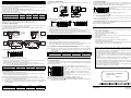
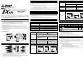
Voltage output
3. Connection with PLC
1) Up to 4 FX0N-3A units can connect to the FX0N series PLC, up to 5 for FX1N, up to 8 for FX2N or, up to
4 for an FX 2NC series PLC, all with powered extension units.
However the following limitation exists when the undermentioned special function blocks are connected.
FX2N:
Main unit and powered extension units of 32 I/O points or less. Consumption current available for
undermentioned special function blocks ≤ 190mA
FX2N:
Main unit and powered extension units of 48 I/O points or more. Consumption current available
for undermentioned special function blocks ≤ 300mA
Analog output range
DC 0 to 10V, 0 to 5V external load:
1kΩ to 1MΩ
8 bits
40mV: 0 to 10V/0 to 250(At shipment)
Change depending on the input
characteristic.
64μA: 4 to 20mA /0 to 250
Change depending on the input
characteristic.
Overall accuracy
± 0.1V
± 0.16mA
Processing time
TO instruction processing time x 3
Smallest output
signal resolution
FX0N/1N: Main unit and powered extension units. Up to 2 undermentioned special function blocks can be
connected regardless of the system I/O.
[At shipment]
0
1
0 .0 2 0
1
0
2 5 0
D IG IT A L V A L U E
3) The FX0N-3A and main unit are connected by a cable on the right of the main unit.
5 .1 V
5
0 .0 4 0
2 0 .3 2 m A
2 0
4 .0 6 4
2 5 5
This manual contains text, diagrams and explanations which will guide the user in the correct installation
and operation of the FX0N-3A special function block and should be read and understood before attempting
to install or use the unit. Further information can be found in the FX PROGRAMMING MANUAL(ΙΙ), FX0N
/FX1N/FX2N/FX2NC SERIES HARDWARE MANUAL.
Output
characteristics
2) FX 0N-3A consumes 5V DC by 30mA. The total 5V consumption of all special function blocks
connected to either the FX2N or FX2NC main unit or an FX2N extension unit must not exceed the 5V
voltage source capacity of the system.
1 0
A N A L O G
V O L T S
The consumption current of the above units is to be subtracted from the service power supply of the host
PLC.
1 0 .2 V
O U T P U T m A
90mA
2 5 5
85mA
A N A L O G
50mA
Consumption current of 24V DC for one unit.
JY992D49001F
O U T P U T
FX0N-3A
A N A L O G
V O L T S
FX2N-2DA
2 5 5
FX2N-2AD
O U T P U T
USER’S GUIDE
4 to 20mA, external load: 500Ω or less
Digital resolution
FX2NC: Up to 4 undermentioned special function blocks can be connected regardless of the system I/O.
FX0N-3A SPECIAL FUNCTION BLOCK
Current output
At shipment, 0 to 250 range selected for 0 to 10V DC output.
When using an FX0N-3A for current output or differing voltage output except 0 to
10V DC, it is necessary to readjust the offset and gain.
4
0
2 5 0
D IG IT A L V A L U E
1
D IG IT A L V A L U E
2 5 0
If digital source data of greater than 8 bits is used, only the lower 8 bits will be
valid. Additional (upper) bits will be ignored
1. Introduction
4. Installation notes and Usage
•
4.1 General and Environmental Specifications
The FX0N-3A analog special function block has two input channels and one output channel.
The input channels receive analog signals and convert them into digital values.
The output channel takes a digital value and outputs an equivalent analog signal.
The FX0N-3A has a maximum resolution of 8 bits.
•
The selection of voltage or current based input/output is decided by user wiring.
•
An FX0N-3A can connected to the FX2N, FX2NC, FX1N or FX0N series of Programmable Controllers
(Hereafter referred to as a PLC).
•
All data transfers and parameter setups are adjusted through software control for the FX0N-3A, via
TO/FROM applied instructions in the PLC. Communications between the PLC and FX0N-3A are
protected by a photo-coupler.
An FX0N-3A occupies 8 I/O points on the PLC’s expansion bus. The 8 I/O points can be allocated from
either inputs or outputs.
1.1 External Dimensions
Item
Withstand Voltage
500V AC for 1 minute (between ground and all other terminals)
BFM
No.
Analog circuit power requirement
24V DC +/- 10%, 90mA (internal power supply from main unit)
0
Digital circuit power requirement
5V DC, 30mA (internal power supply from main unit)
16
Isolation
Photo-coupler isolation between analog and digital circuit.
No isolation between analog channels.
17
Number of occupied I/O points
8 I/O points from expansion bus. (either input or output)
Dimensions: mm (inches)
Voltage input
V
V
IN
1
IN
V
IN
3 5 m m
D IN r a il
g ro o v e
1
V
2
E x te n s io n
c a b le
IN
I IN 1
A /D
9 0 (3 .5 4 )
8 0 (3 .1 5 )
2
I IN 2 C O M 2
C O M 1
C O M
C O M
IIN 1
IIN 2
P O W E R
O F F S E T
P O W E R
Analog input range
A /D
G A IN
D /A
IO
O F F S E T
D /A
V
C O M
C O M
O U T
O U T
V
8 7 (3 .4 3 )
U T
9 (0 .3 5 )
IO
M o u n tin g h o le ,
2 h o le s 4 .5
( 0 .1 8 ) d ia
U T
G A IN
M 3 (0 .1 2 )
te r m in a l s c r e w s
4 (0 .1 6 )
4 3 (1 .6 9 )
Overall accuracy
± 0.1V
± 0.16mA
Processing time
TO instruction processing time x 2 + FROM instruction processing time
C O M
C O M 2
C O M 1
Input characteristics
V
IO
IN
V
V
U T
1
IN
IIN 2
C O M
I IN 1
O U T
2
C O M 2
C O M 1
C u rre n t
o u tp u t
2 5 5
2 5 0
2 5 0
0
0 .0 4 0
A N A L O G
1 0
IN P U T V O L T S
1
0
0 .0 2 0
A N A L O G
5
IN P U T V O L T S
1
0
4
A N A L O G
4 .0 6 4
IN P U T m A
2 0
The module does not allow different input characteristics for two channels.
•
When a current input is used, ensure that the terminals marked [VIN*1] and [IIN*1] are linked.
Do not connect the [VOUT] and [IOUT] terminals when the current output is used.
*1 terminal number 1 or 2 is identified here.
•
If any voltage ripple is experienced on the voltage inputs/outputs or if there is excessive electrical
noise, connect a capacitor of 0.1 to 0.47μF, approx. 25V rating at position *2.
b4
b3
b2
b1
b0
Current value input data (stored in 8 bits) of the A/D channel selected by b0 of BFM#17
Current value output data on D/A channel (stored in 8 bits)
D/A
start
Reserved
A/D
start
A/D
channel
Reserved
•
BFM 17:
b0 = 0 analog input channel 1 is selected
b0 = 1 analog input channel 2 is selected
b1 = 0 Ö1, the A/D conversion process is started
b2 = 1 Ö 0, the D/A conversion process is started
•
Note: These buffer memory devices are stored/located within the FX0N-3A
6. Diagnostics
6.1 Preliminary Checks
a) Check whether the input/output wiring and/or expansion cables are properly connected.
d) As the status of the PLC changes (RUN Ö STOP, STOP Ö RUN, etc.), the analog output status will
operate in the following manner.
2 5 5
2 5 0
1
b5
c) Ensure that the correct operating range has been selected for the application.
2 0 .3 2 m A
O U T
IIN 2
+
V o lta g e
o u tp u t
b6
Status change of the host PLC:
D IG IT A L V A L U E
V
U T
I IN 1
+
5 .1 V
2
*2
IO
IN
+
64μA: 4 to 20mA /0 to 250
Change depending on the input
characteristic.
1 0 .2 V
1
*2
C H 2
40mV: 0 to 10V/0 to 250(At shipment)
Change depending on the input
characteristic.
D IG IT A L V A L U E
V
V o lta g e
in p u t
+
C H 1
Smallest input signal resolution
2 5 5
Reserved
b7
b) Check that the system configuration rules for the host PLC have not been broken.
[At shipment]
IN
+
C H 2
4 to 20mA, resistance 250Ω. Warning:
this unit may be damaged by input
currents in excess of -2mA, +60mA.
8 bits
V
C u rre n t
in p u t
At shipment, 0 to 250 range selected for 0 to 10V DC input.
When using an FX0N-3A for current input or differing voltage inputs except 0 to
10V DC, it is necessary to readjust the offset and gain.
The module does not allow different input characteristics for two channels.
0 to 10V, 0 to 5V DC, resistance
200kΩ. Warning: this unit may be
damaged by input voltages in excess
of -0.5V, +15V.
b15-b8
1-5,
18-31
Current input
Digital resolution
2. Terminal layouts and wiring
+
When FNC176(RD3A) and FNC177(WR3A) are used with FX1N,FX2N (V3.00 or more) or FX2NC (V3.00 or
more), the allocation of the buffer memory (BFM) need not be considered.
Same as those for the main unit
4.2 Performance Specifications
Mass: Approx. 0.2kg (0.44lbs)
C H 1
Specification
General specifications
(ex. withstand voltage)
D IG IT A L V A L U E
•
5. Allocation of Buffer Memories (BFM)
-
RUN Ö STOP: The last operational value used by the analog output channel during RUN
operation is retained during STOP mode.
-
STOP Ö RUN: Once the host PLC is switched back into RUN mode the analog output reacts as
normal to the program controlled, digital values.
PLC power shutdown: The analog output signal ceases operation.
e) Remember that only 8 bit digital values (0 to 255) are valid for use with the analog output of the
FX0N-3A
7. Change and adjustment method of input/output characteristic
7.1 Change in input/output characteristic
7.3 Method of Calibration(D/A)
8.2 Using Analog Outputs
Use the following program and the appropriate wiring configuration to calibrate the output channel of the
FX0N-3A
The buffer memories (BFM) of the FX 0N-3A are written TO, or read FROM by the host PLC. In the
following program, when M0 is turned ON the D/A conversion process is executed and an analog signal
equivalent to the digital value stored in this example, is output to register D02
At shipment, 0 to 250 range selected for 0 to 10V DC input/output.
When using an FX0N-3A for current input/output or differing voltage input/output except 0 to 10V DC, it is
necessary to readjust the offset and gain.
The module does not allow different input characteristics for two channels.
Set analog values from 0 to 250 digital equivalent within the range specified in the table below when
changing the input/output characteristic.
A/D
A/D
D/A
D/A
D/A
D/A
GAIN
GAIN
OFFSET
Voltage
output
M0
OFFSET
GAIN
Current
output
GAIN
VOUT
IOUT COM
VOUT
IOUT COM
Range of allowance of input/output characteristic
Voltage
input
Current
input
Voltage
output
Current
output
Analog value when digital value is 0
0 to 1V
0 to 4mA
0V
4mA
Analog value when digital value is 250
5 to 10V
20mA
5 to 10V
20mA
+
Voltmeter
X00
X00
7.2 Method of Calibration(A/D)
O F F S E T
A
V o ltm e te r
+
+
C u rre n t g e n e ra to r
+
V IN 2
IIN 2 C O M 2
IIN 1 C O M 1
V IN 1
O F F S E T
G A IN
C O M
In te g ra l
c u rre n t
in p u t
+
K0
K16
K1
K1
TO
K0
K16 K250
K1
TO
K0
K17
H04
K1
TO
K0
K17
H04
K1
TO
K0
K17
H00
K1
TO
K0
K17
H00
K1
X02
K0
K17
H00
K1
TO
K0
K17
H02
K1
2) Adjust the D/A OFFSET potentiometer (‘pot) until the selected meter displays the appropriate offset
voltage/current (in accordance with the analog operation range selected, see table below).
1) Run the previously detailed program. Ensure X02 is ON.
2) Generate an offset voltage/current (in accordance with the analog operation range to be selected, see
table below) using the selected generator or analog output.
3) Adjust the A/D OFFSET potentiometer (‘pot’) until a digital value of 1 is read in D00.
Note : Turn the ‘pot’ clockwise and the digital value will increase. The ‘pot’ requires 18 revolutions to
move between the minimum and maximum settings.
Analog output range
0-10V DC
0-5V DC
4-20mA DC
Offset calibration meter value
0.040V
0.020V
4.064mA
1) Run the previously detailed program. Ensure X00 is OFF and X01 is ON.
2) Adjust the D/A GAIN potentiometer (‘pot’) until selected meter displays the appropriate gain voltage/
current (in accordance with the analog operation range selected, see table below).
K1
TO
K0
K17
H00
K1
If the FX0N-3A special function block does not seem to operate normally, check the following items:
•
Check the status of POWER LED.
Lit: The extension cable is properly connected.
Otherwise: Check the connection of the extension cable.
•
Check the external wiring.
•
Check whether the output load connected to the analog output terminal is within the following
specified limits.
Voltage output: 1kΩ to 1MΩ, Current output: 500Ω or less
•
Check whether the impedance of the input device is within the specified limits.
Voltage input: 200kΩ, Current input: 250Ω.
•
Check the calibration of the FX0N-3A’s analog channels (input and output) using a voltmeter/ ammeter
as required. See previous two sections for a detailed explanation.
Guidelines for the safety of the user and protection of the FX0N-3A Special
function block
•
This manual has been written to be used by trained and competent personnel. This is defined
by the European directives for machinery and EMC.
•
If in doubt at any stage during the installation of the FX0N-3A always consult a professional
electrical engineer who is qualified and trained to the local and national standards. If in doubt
about the operation or use of the FX 0N-3A please consult the nearest Mitsubishi Electric
distributor.
8. Program example
•
Under no circumstances will Mitsubishi Electric be liable or responsible for any consequential
damage that may arise as a result of the installation or use of this equipment.
8.1 Using Analog Inputs
•
The buffer memories (BFM) of the FX0N-3A are written TO or read FROM by the host PLC. The following
program reads the analog input from channel 1 of the FX0N-3A when M0 is ON, and the analog input data
of channel 2 when M1 is ON.
All examples and diagrams shown in this manual are intended only as an aid to understanding
the text, not to guarantee operation. Mitsubishi Electric will accept no responsibility for actual
use of the product based on these illustrative examples.
•
Owing to the very great variety in possible application of this equipment, you must satisfy
yourself as to its suitability for your specific application.
M0
Offset calibration value
H04
Please use FNC 176 (RD3A) and FNC 177 (WR3A)
Refer to FX Series Programming Manual ΙΙ.
0-10V DC
0-5V DC
4-20mA DC
10.000V
5.000V
20.000mA
K1
7.2.2 Calibrating the Offset
Analog input range
K17
8.3 Using FX1N, FX2N (V3.00 or more) or FX2NC (V3.00 or more) Series PLC’s
Note: Turn the ‘pot’ clockwise and the analog output signal will increase. The ‘pot’ requires 18 revolutions
to move between the minimum and maximum settings.
Analog output range
D0
K0
9. Error Checking
Gain calibration meter value
K0
TO
The contents of D2 are written to BFM#16. This will be converted to
an analog output.
(H04) is written to BFM#17 to start the D/A conversion process.
1) Run the previously detailed program. Ensure X00 is ON and X01 is OFF.
Note 2: When it is necessary to maximize the 8 bit resolution, the digital value used in the gain adjustment
(detailed above) should be replaced with 255. This section has been written to demonstrate a 250
full scale calibration.
TO
K1
Note 1: Turn the ‘pot’ clockwise and the analog output signal will increase. The ‘pot’ requires 18
revolutions to move between the minimum and maximum settings
7.2.1 Input Calibration Program
FROM K0
X01
TO
7.3.3 Calibrating the Gain
O U T
D /A
A /D
A
V
V
U T
G A IN
IO
O F F S E T
C O M
D /A
O U T
A /D
V
U T
G A IN
A /D
A /D
O F F S E T
In te g ra l
v o lta g e
in p u t
O F F S E T
IO
P O W E R
I IN 2 C O M 2
C O M 1
G A IN
IIN 1
D /A
2
D /A
IN
1
P O W E R
V
IN
D02
Details on both the FROM and TO instructions (functions 78 and 79 respectively) can be found in the
“FX series Programming Manual (ΙΙ)”
7.3.2 Calibrating the Offset
A m m e te r
V o lta g e g e n e r a to r
V
E x te rn a l
c u rre n t
in p u t
K16
Note : The 3 (TO) instruction format shown above should always be used when writing data to the
FX0N-3A’s analog output channel.
A /D
O F F S E T
O F F S E T
G A IN
G A IN
A /D
V
1
IN
I IN 2 C O M 2
I IN 1 C O M 1
D /A
A /D
O F F S E T
A /D
+
V
A /D G A IN
D /A O F F S E T
D /A G A IN
2
IN
P O W E R
V
IIN 2 C O M 2
I IN 1 C O M 1
D /A
1
IN
2
IN
P O W E R
V
E x te rn a l
v o lta g e
in p u t
V
A
Ammeter
X01
K0
The time TAD required to write an analog input channel is calculated as follows:
TAD = (TO instruction processing time) × 3
7.3.1 Output Calibration Program
Resolution changes depending on the set value when the input/output characteristic is changed.
Example: Resolution becomes (5 to 0V)/250=20mV at voltage input 0 to 5V/0 to 250.
Overall accuracy does not change. (Voltage input: ±0.1V, Current input: ±0.16mA)
Both analog input channels share the same ‘setup’ and configuration. Hence only one channel needs to
be selected to perform the calibration for both analog input channels.
Use the following program and the appropriate wiring configuration to calibrate input channel 1 (and
indirectly channel 2) of the FX0N-3A.
+
V
TO
0-10V DC
0-5V DC
4-20mA DC
0.040V
0.020V
4.064mA
TO
K0
K17
H00
K1
TO
K0
K17
H02
K1
K0
D00
K1
FROM K0
M1
7.2.3 Calibrating the Gain
1) Run the previously detailed program. Ensure X02 is ON.
2) Generate a gain voltage/current (in accordance with the analog operation range to be selected, see
table below) using the selected generator or analog output.
3) Adjust the A/D GAIN potentiometer (‘pot’) until a digital value of 250 is read in D00.
Note 1: Turn the ‘pot’ clockwise and the digital value will increase. The ‘pot’ requires 18 revolutions to
move between the minimum and maximum settings.
Note 2: When necessary to maximize the 8 bit resolution, the digital value used in the gain adjustment
(detailed above) should be replaced with 255. This section has been written to demonstrate 250
full scale calibration.
TO
K0
K17
H01
K1
TO
K0
K17
H03
K1
K0
D01
K1
FROM K0
(H00) is written to BFM#17, selecting A/D input channel 1.
(H02) is written to BFM#17 starting the A/D conversion process for
channel 1.
BFM#0 is read, storing the current value of channel 1 in register
D00
(H01) is written to BFM#17 now selecting A/D input channel 2.
(H03) is written to BFM#17 to re-start the A/D conversion process,
but for channel 2.
BFM#0 is read, storing the current value of channel 2 in register
D01.
Manual number : JY992D49001
Manual revision : F
The time TAD required to read an analog input channel is calculated as follows:
TAD = (TO instruction processing time) × 2 + (FROM instruction processing time)
Date
: April 2015
Note : The 3 (TO/FROM) command format shown above should always be used when reading data from
the FX0N-3A’s analog input channels.
HEAD OFFICE : TOKYO BUILDING, 2-7-3 MARUNOUCHI, CHIYODA-KU, TOKYO 100-8310, JAPAN
Analog input range
Gain calibration value
0-10V DC
0-5V DC
4-20mA DC
10.000V
5.000V
20.000mA
JY992D49001F
Effective April 2015
Specifications are subject to
change without notice
Voltage output
3. Connection with PLC
1) Up to 4 FX0N-3A units can connect to the FX0N series PLC, up to 5 for FX1N, up to 8 for FX2N or, up to
4 for an FX 2NC series PLC, all with powered extension units.
However the following limitation exists when the undermentioned special function blocks are connected.
FX2N:
Main unit and powered extension units of 32 I/O points or less. Consumption current available for
undermentioned special function blocks ≤ 190mA
FX2N:
Main unit and powered extension units of 48 I/O points or more. Consumption current available
for undermentioned special function blocks ≤ 300mA
Analog output range
DC 0 to 10V, 0 to 5V external load:
1kΩ to 1MΩ
8 bits
40mV: 0 to 10V/0 to 250(At shipment)
Change depending on the input
characteristic.
64μA: 4 to 20mA /0 to 250
Change depending on the input
characteristic.
Overall accuracy
± 0.1V
± 0.16mA
Processing time
TO instruction processing time x 3
Smallest output
signal resolution
FX0N/1N: Main unit and powered extension units. Up to 2 undermentioned special function blocks can be
connected regardless of the system I/O.
[At shipment]
0
1
0 .0 2 0
1
0
2 5 0
D IG IT A L V A L U E
3) The FX0N-3A and main unit are connected by a cable on the right of the main unit.
5 .1 V
5
0 .0 4 0
2 0 .3 2 m A
2 0
4 .0 6 4
2 5 5
This manual contains text, diagrams and explanations which will guide the user in the correct installation
and operation of the FX0N-3A special function block and should be read and understood before attempting
to install or use the unit. Further information can be found in the FX PROGRAMMING MANUAL(ΙΙ), FX0N
/FX1N/FX2N/FX2NC SERIES HARDWARE MANUAL.
Output
characteristics
2) FX 0N-3A consumes 5V DC by 30mA. The total 5V consumption of all special function blocks
connected to either the FX2N or FX2NC main unit or an FX2N extension unit must not exceed the 5V
voltage source capacity of the system.
1 0
A N A L O G
V O L T S
The consumption current of the above units is to be subtracted from the service power supply of the host
PLC.
1 0 .2 V
O U T P U T m A
90mA
2 5 5
85mA
A N A L O G
50mA
Consumption current of 24V DC for one unit.
JY992D49001F
O U T P U T
FX0N-3A
A N A L O G
V O L T S
FX2N-2DA
2 5 5
FX2N-2AD
O U T P U T
USER’S GUIDE
4 to 20mA, external load: 500Ω or less
Digital resolution
FX2NC: Up to 4 undermentioned special function blocks can be connected regardless of the system I/O.
FX0N-3A SPECIAL FUNCTION BLOCK
Current output
At shipment, 0 to 250 range selected for 0 to 10V DC output.
When using an FX0N-3A for current output or differing voltage output except 0 to
10V DC, it is necessary to readjust the offset and gain.
4
0
2 5 0
D IG IT A L V A L U E
1
D IG IT A L V A L U E
2 5 0
If digital source data of greater than 8 bits is used, only the lower 8 bits will be
valid. Additional (upper) bits will be ignored
1. Introduction
4. Installation notes and Usage
•
4.1 General and Environmental Specifications
The FX0N-3A analog special function block has two input channels and one output channel.
The input channels receive analog signals and convert them into digital values.
The output channel takes a digital value and outputs an equivalent analog signal.
The FX0N-3A has a maximum resolution of 8 bits.
•
The selection of voltage or current based input/output is decided by user wiring.
•
An FX0N-3A can connected to the FX2N, FX2NC, FX1N or FX0N series of Programmable Controllers
(Hereafter referred to as a PLC).
•
All data transfers and parameter setups are adjusted through software control for the FX0N-3A, via
TO/FROM applied instructions in the PLC. Communications between the PLC and FX0N-3A are
protected by a photo-coupler.
An FX0N-3A occupies 8 I/O points on the PLC’s expansion bus. The 8 I/O points can be allocated from
either inputs or outputs.
1.1 External Dimensions
Item
Withstand Voltage
500V AC for 1 minute (between ground and all other terminals)
BFM
No.
Analog circuit power requirement
24V DC +/- 10%, 90mA (internal power supply from main unit)
0
Digital circuit power requirement
5V DC, 30mA (internal power supply from main unit)
16
Isolation
Photo-coupler isolation between analog and digital circuit.
No isolation between analog channels.
17
Number of occupied I/O points
8 I/O points from expansion bus. (either input or output)
Dimensions: mm (inches)
Voltage input
V
V
IN
1
IN
V
IN
3 5 m m
D IN r a il
g ro o v e
1
V
2
E x te n s io n
c a b le
IN
I IN 1
A /D
9 0 (3 .5 4 )
8 0 (3 .1 5 )
2
I IN 2 C O M 2
C O M 1
C O M
C O M
IIN 1
IIN 2
P O W E R
O F F S E T
P O W E R
Analog input range
A /D
G A IN
D /A
IO
O F F S E T
D /A
V
C O M
C O M
O U T
O U T
V
8 7 (3 .4 3 )
U T
9 (0 .3 5 )
IO
M o u n tin g h o le ,
2 h o le s 4 .5
( 0 .1 8 ) d ia
U T
G A IN
M 3 (0 .1 2 )
te r m in a l s c r e w s
4 (0 .1 6 )
4 3 (1 .6 9 )
Overall accuracy
± 0.1V
± 0.16mA
Processing time
TO instruction processing time x 2 + FROM instruction processing time
C O M
C O M 2
C O M 1
Input characteristics
V
IO
IN
V
V
U T
1
IN
IIN 2
C O M
I IN 1
O U T
2
C O M 2
C O M 1
C u rre n t
o u tp u t
2 5 5
2 5 0
2 5 0
0
0 .0 4 0
A N A L O G
1 0
IN P U T V O L T S
1
0
0 .0 2 0
A N A L O G
5
IN P U T V O L T S
1
0
4
A N A L O G
4 .0 6 4
IN P U T m A
2 0
The module does not allow different input characteristics for two channels.
•
When a current input is used, ensure that the terminals marked [VIN*1] and [IIN*1] are linked.
Do not connect the [VOUT] and [IOUT] terminals when the current output is used.
*1 terminal number 1 or 2 is identified here.
•
If any voltage ripple is experienced on the voltage inputs/outputs or if there is excessive electrical
noise, connect a capacitor of 0.1 to 0.47μF, approx. 25V rating at position *2.
b4
b3
b2
b1
b0
Current value input data (stored in 8 bits) of the A/D channel selected by b0 of BFM#17
Current value output data on D/A channel (stored in 8 bits)
D/A
start
Reserved
A/D
start
A/D
channel
Reserved
•
BFM 17:
b0 = 0 analog input channel 1 is selected
b0 = 1 analog input channel 2 is selected
b1 = 0 Ö1, the A/D conversion process is started
b2 = 1 Ö 0, the D/A conversion process is started
•
Note: These buffer memory devices are stored/located within the FX0N-3A
6. Diagnostics
6.1 Preliminary Checks
a) Check whether the input/output wiring and/or expansion cables are properly connected.
d) As the status of the PLC changes (RUN Ö STOP, STOP Ö RUN, etc.), the analog output status will
operate in the following manner.
2 5 5
2 5 0
1
b5
c) Ensure that the correct operating range has been selected for the application.
2 0 .3 2 m A
O U T
IIN 2
+
V o lta g e
o u tp u t
b6
Status change of the host PLC:
D IG IT A L V A L U E
V
U T
I IN 1
+
5 .1 V
2
*2
IO
IN
+
64μA: 4 to 20mA /0 to 250
Change depending on the input
characteristic.
1 0 .2 V
1
*2
C H 2
40mV: 0 to 10V/0 to 250(At shipment)
Change depending on the input
characteristic.
D IG IT A L V A L U E
V
V o lta g e
in p u t
+
C H 1
Smallest input signal resolution
2 5 5
Reserved
b7
b) Check that the system configuration rules for the host PLC have not been broken.
[At shipment]
IN
+
C H 2
4 to 20mA, resistance 250Ω. Warning:
this unit may be damaged by input
currents in excess of -2mA, +60mA.
8 bits
V
C u rre n t
in p u t
At shipment, 0 to 250 range selected for 0 to 10V DC input.
When using an FX0N-3A for current input or differing voltage inputs except 0 to
10V DC, it is necessary to readjust the offset and gain.
The module does not allow different input characteristics for two channels.
0 to 10V, 0 to 5V DC, resistance
200kΩ. Warning: this unit may be
damaged by input voltages in excess
of -0.5V, +15V.
b15-b8
1-5,
18-31
Current input
Digital resolution
2. Terminal layouts and wiring
+
When FNC176(RD3A) and FNC177(WR3A) are used with FX1N,FX2N (V3.00 or more) or FX2NC (V3.00 or
more), the allocation of the buffer memory (BFM) need not be considered.
Same as those for the main unit
4.2 Performance Specifications
Mass: Approx. 0.2kg (0.44lbs)
C H 1
Specification
General specifications
(ex. withstand voltage)
D IG IT A L V A L U E
•
5. Allocation of Buffer Memories (BFM)
-
RUN Ö STOP: The last operational value used by the analog output channel during RUN
operation is retained during STOP mode.
-
STOP Ö RUN: Once the host PLC is switched back into RUN mode the analog output reacts as
normal to the program controlled, digital values.
PLC power shutdown: The analog output signal ceases operation.
e) Remember that only 8 bit digital values (0 to 255) are valid for use with the analog output of the
FX0N-3A
7. Change and adjustment method of input/output characteristic
7.1 Change in input/output characteristic
7.3 Method of Calibration(D/A)
8.2 Using Analog Outputs
Use the following program and the appropriate wiring configuration to calibrate the output channel of the
FX0N-3A
The buffer memories (BFM) of the FX 0N-3A are written TO, or read FROM by the host PLC. In the
following program, when M0 is turned ON the D/A conversion process is executed and an analog signal
equivalent to the digital value stored in this example, is output to register D02
At shipment, 0 to 250 range selected for 0 to 10V DC input/output.
When using an FX0N-3A for current input/output or differing voltage input/output except 0 to 10V DC, it is
necessary to readjust the offset and gain.
The module does not allow different input characteristics for two channels.
Set analog values from 0 to 250 digital equivalent within the range specified in the table below when
changing the input/output characteristic.
A/D
A/D
D/A
D/A
D/A
D/A
GAIN
GAIN
OFFSET
Voltage
output
M0
OFFSET
GAIN
Current
output
GAIN
VOUT
IOUT COM
VOUT
IOUT COM
Range of allowance of input/output characteristic
Voltage
input
Current
input
Voltage
output
Current
output
Analog value when digital value is 0
0 to 1V
0 to 4mA
0V
4mA
Analog value when digital value is 250
5 to 10V
20mA
5 to 10V
20mA
+
Voltmeter
X00
X00
7.2 Method of Calibration(A/D)
O F F S E T
A
V o ltm e te r
+
+
C u rre n t g e n e ra to r
+
V IN 2
IIN 2 C O M 2
IIN 1 C O M 1
V IN 1
O F F S E T
G A IN
C O M
In te g ra l
c u rre n t
in p u t
+
K0
K16
K1
K1
TO
K0
K16 K250
K1
TO
K0
K17
H04
K1
TO
K0
K17
H04
K1
TO
K0
K17
H00
K1
TO
K0
K17
H00
K1
X02
K0
K17
H00
K1
TO
K0
K17
H02
K1
2) Adjust the D/A OFFSET potentiometer (‘pot) until the selected meter displays the appropriate offset
voltage/current (in accordance with the analog operation range selected, see table below).
1) Run the previously detailed program. Ensure X02 is ON.
2) Generate an offset voltage/current (in accordance with the analog operation range to be selected, see
table below) using the selected generator or analog output.
3) Adjust the A/D OFFSET potentiometer (‘pot’) until a digital value of 1 is read in D00.
Note : Turn the ‘pot’ clockwise and the digital value will increase. The ‘pot’ requires 18 revolutions to
move between the minimum and maximum settings.
Analog output range
0-10V DC
0-5V DC
4-20mA DC
Offset calibration meter value
0.040V
0.020V
4.064mA
1) Run the previously detailed program. Ensure X00 is OFF and X01 is ON.
2) Adjust the D/A GAIN potentiometer (‘pot’) until selected meter displays the appropriate gain voltage/
current (in accordance with the analog operation range selected, see table below).
K1
TO
K0
K17
H00
K1
If the FX0N-3A special function block does not seem to operate normally, check the following items:
•
Check the status of POWER LED.
Lit: The extension cable is properly connected.
Otherwise: Check the connection of the extension cable.
•
Check the external wiring.
•
Check whether the output load connected to the analog output terminal is within the following
specified limits.
Voltage output: 1kΩ to 1MΩ, Current output: 500Ω or less
•
Check whether the impedance of the input device is within the specified limits.
Voltage input: 200kΩ, Current input: 250Ω.
•
Check the calibration of the FX0N-3A’s analog channels (input and output) using a voltmeter/ ammeter
as required. See previous two sections for a detailed explanation.
Guidelines for the safety of the user and protection of the FX0N-3A Special
function block
•
This manual has been written to be used by trained and competent personnel. This is defined
by the European directives for machinery and EMC.
•
If in doubt at any stage during the installation of the FX0N-3A always consult a professional
electrical engineer who is qualified and trained to the local and national standards. If in doubt
about the operation or use of the FX 0N-3A please consult the nearest Mitsubishi Electric
distributor.
8. Program example
•
Under no circumstances will Mitsubishi Electric be liable or responsible for any consequential
damage that may arise as a result of the installation or use of this equipment.
8.1 Using Analog Inputs
•
The buffer memories (BFM) of the FX0N-3A are written TO or read FROM by the host PLC. The following
program reads the analog input from channel 1 of the FX0N-3A when M0 is ON, and the analog input data
of channel 2 when M1 is ON.
All examples and diagrams shown in this manual are intended only as an aid to understanding
the text, not to guarantee operation. Mitsubishi Electric will accept no responsibility for actual
use of the product based on these illustrative examples.
•
Owing to the very great variety in possible application of this equipment, you must satisfy
yourself as to its suitability for your specific application.
M0
Offset calibration value
H04
Please use FNC 176 (RD3A) and FNC 177 (WR3A)
Refer to FX Series Programming Manual ΙΙ.
0-10V DC
0-5V DC
4-20mA DC
10.000V
5.000V
20.000mA
K1
7.2.2 Calibrating the Offset
Analog input range
K17
8.3 Using FX1N, FX2N (V3.00 or more) or FX2NC (V3.00 or more) Series PLC’s
Note: Turn the ‘pot’ clockwise and the analog output signal will increase. The ‘pot’ requires 18 revolutions
to move between the minimum and maximum settings.
Analog output range
D0
K0
9. Error Checking
Gain calibration meter value
K0
TO
The contents of D2 are written to BFM#16. This will be converted to
an analog output.
(H04) is written to BFM#17 to start the D/A conversion process.
1) Run the previously detailed program. Ensure X00 is ON and X01 is OFF.
Note 2: When it is necessary to maximize the 8 bit resolution, the digital value used in the gain adjustment
(detailed above) should be replaced with 255. This section has been written to demonstrate a 250
full scale calibration.
TO
K1
Note 1: Turn the ‘pot’ clockwise and the analog output signal will increase. The ‘pot’ requires 18
revolutions to move between the minimum and maximum settings
7.2.1 Input Calibration Program
FROM K0
X01
TO
7.3.3 Calibrating the Gain
O U T
D /A
A /D
A
V
V
U T
G A IN
IO
O F F S E T
C O M
D /A
O U T
A /D
V
U T
G A IN
A /D
A /D
O F F S E T
In te g ra l
v o lta g e
in p u t
O F F S E T
IO
P O W E R
I IN 2 C O M 2
C O M 1
G A IN
IIN 1
D /A
2
D /A
IN
1
P O W E R
V
IN
D02
Details on both the FROM and TO instructions (functions 78 and 79 respectively) can be found in the
“FX series Programming Manual (ΙΙ)”
7.3.2 Calibrating the Offset
A m m e te r
V o lta g e g e n e r a to r
V
E x te rn a l
c u rre n t
in p u t
K16
Note : The 3 (TO) instruction format shown above should always be used when writing data to the
FX0N-3A’s analog output channel.
A /D
O F F S E T
O F F S E T
G A IN
G A IN
A /D
V
1
IN
I IN 2 C O M 2
I IN 1 C O M 1
D /A
A /D
O F F S E T
A /D
+
V
A /D G A IN
D /A O F F S E T
D /A G A IN
2
IN
P O W E R
V
IIN 2 C O M 2
I IN 1 C O M 1
D /A
1
IN
2
IN
P O W E R
V
E x te rn a l
v o lta g e
in p u t
V
A
Ammeter
X01
K0
The time TAD required to write an analog input channel is calculated as follows:
TAD = (TO instruction processing time) × 3
7.3.1 Output Calibration Program
Resolution changes depending on the set value when the input/output characteristic is changed.
Example: Resolution becomes (5 to 0V)/250=20mV at voltage input 0 to 5V/0 to 250.
Overall accuracy does not change. (Voltage input: ±0.1V, Current input: ±0.16mA)
Both analog input channels share the same ‘setup’ and configuration. Hence only one channel needs to
be selected to perform the calibration for both analog input channels.
Use the following program and the appropriate wiring configuration to calibrate input channel 1 (and
indirectly channel 2) of the FX0N-3A.
+
V
TO
0-10V DC
0-5V DC
4-20mA DC
0.040V
0.020V
4.064mA
TO
K0
K17
H00
K1
TO
K0
K17
H02
K1
K0
D00
K1
FROM K0
M1
7.2.3 Calibrating the Gain
1) Run the previously detailed program. Ensure X02 is ON.
2) Generate a gain voltage/current (in accordance with the analog operation range to be selected, see
table below) using the selected generator or analog output.
3) Adjust the A/D GAIN potentiometer (‘pot’) until a digital value of 250 is read in D00.
Note 1: Turn the ‘pot’ clockwise and the digital value will increase. The ‘pot’ requires 18 revolutions to
move between the minimum and maximum settings.
Note 2: When necessary to maximize the 8 bit resolution, the digital value used in the gain adjustment
(detailed above) should be replaced with 255. This section has been written to demonstrate 250
full scale calibration.
TO
K0
K17
H01
K1
TO
K0
K17
H03
K1
K0
D01
K1
FROM K0
(H00) is written to BFM#17, selecting A/D input channel 1.
(H02) is written to BFM#17 starting the A/D conversion process for
channel 1.
BFM#0 is read, storing the current value of channel 1 in register
D00
(H01) is written to BFM#17 now selecting A/D input channel 2.
(H03) is written to BFM#17 to re-start the A/D conversion process,
but for channel 2.
BFM#0 is read, storing the current value of channel 2 in register
D01.
Manual number : JY992D49001
Manual revision : F
The time TAD required to read an analog input channel is calculated as follows:
TAD = (TO instruction processing time) × 2 + (FROM instruction processing time)
Date
: April 2015
Note : The 3 (TO/FROM) command format shown above should always be used when reading data from
the FX0N-3A’s analog input channels.
HEAD OFFICE : TOKYO BUILDING, 2-7-3 MARUNOUCHI, CHIYODA-KU, TOKYO 100-8310, JAPAN
Analog input range
Gain calibration value
0-10V DC
0-5V DC
4-20mA DC
10.000V
5.000V
20.000mA
JY992D49001F
Effective April 2015
Specifications are subject to
change without notice