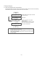
1
Remote I/O & Remote Motion
G9001A/G9002
(Center device / I/O device)
User's Manual
Nippon Pulse Motor Co., Ltd.
[Preface]
Thank you for considering our super high-speed serial communicator LSI, the "G9000."
To learn how to use the G9000, read this manual to become familiar with the product.
The handling precautions for installing this LSI are described at the end of this manual. Make sure to
[What Motionnet is]
As a next generation communication system, the Motionnet can construct faster and more volume
large, scale-systems with wire saving than conventional T-NET system (conventional LSI product to
construct serial communication system by NPM). Further, it has data communication function which
the T-NET does not have, so that it can control data control devices such as PCL series (pulse train
generation LSI made by NPM).
The Motionnet system consists of one center device connected to a CPU bus, a maximum of 64 local
devices, all connected using cables of two or three conductive cores
[Cautions]
(1) Copying all or any part of this manual without written approval is prohibited.
(2) The specifications of this LSI may be changed to improve performance or quality without prior
notice.
(3) Although this manual was produced with the utmost care, if you find any points that are unclear,
wrong, or have inadequate descriptions, please let us know.
[Logic indicators]
(1) Terminal names and signal names that start with a # use negative logic.
Ex.: #CS means that the CS terminal uses negative logic. This has the same meaning as
(2) The expression: PCL device (G9x03) and data device (G9x03) means G9003 and G9103
Motionnet Pulse Control LSI. (G9103 is our product under development as of April 2009.)
INDEX
I. Center device (G9001A) .............................................................................................I-1
1. Outline .................................................................................................................................................... I-3
2. Features.................................................................................................................................................. I-3
3. General specifications ............................................................................................................................ I-4
3-1. Communication system specifications ........................................................................................... I-4
3-2. Center device specifications (G9001A) .......................................................................................... I-5
4. Hardware description.............................................................................................................................. I-6
4-1. A list of terminals (QFP-64)............................................................................................................. I-6
4-2. Terminal allocation diagram............................................................................................................ I-8
4-3. Entire block diagram....................................................................................................................... I-9
4-4. Functions of terminals .................................................................................................................. I-10
4-4-1. CLK ........................................................................................................................................ I-10
4-4-2. #RST ...................................................................................................................................... I-10
4-4-3. CKSL...................................................................................................................................... I-10
4-4-4. IF0, IF1....................................................................................................................................I-11
4-4-5. #CS .........................................................................................................................................I-11
4-4-6. #RD, #WR, A0 and #WRQ......................................................................................................I-11
4-4-7. #INT ........................................................................................................................................I-11
4-4-8. #IFB.........................................................................................................................................I-11
4-4-9. A1 to A8...................................................................................................................................I-11
4-4-10. D0 to D7 ................................................................................................................................I-11
4-4-11. D8 to D15 ............................................................................................................................. I-12
4-4-12. SPD0, SPD1 ........................................................................................................................ I-12
4-4-13. SO ........................................................................................................................................ I-12
4-4-14. SOEH, #SOEL ..................................................................................................................... I-12
4-4-15. SIA, SIB................................................................................................................................ I-12
4-4-16. #MCRY................................................................................................................................. I-13
4-4-17. #MERR................................................................................................................................. I-13
4-4-18. #MERF ................................................................................................................................. I-13
4-4-19. MSYN................................................................................................................................... I-13
4-5. Address map................................................................................................................................. I-14
4-5-1. "Device information" area....................................................................................................... I-18
4-5-2. "Cyclic communication area flags"......................................................................................... I-19
4-5-3. "Change to Input Port Interrupt Setting" area ........................................................................ I-20
4-5-4. "Change-In-Input Interrupt Flag" area.................................................................................... I-21
4-5-5. "Port data" area...................................................................................................................... I-21
4-6. Status............................................................................................................................................ I-22
4-7. Interrupt status.............................................................................................................................. I-24
4-8. Command ..................................................................................................................................... I-25
4-8-1. Operation command............................................................................................................... I-25
4-8-2. Memory access command ..................................................................................................... I-28
4-8-3. Register access command..................................................................................................... I-29
4-9. Register ........................................................................................................................................ I-30
4-9-1. RENV0 register ...................................................................................................................... I-30
4-9-2. RERCNT ................................................................................................................................ I-31
4-9-3. RSYCNT ................................................................................................................................ I-31
4-9-4. RDJADD................................................................................................................................. I-31
4-9-5. RVER ..................................................................................................................................... I-31
5. Description of the software ................................................................................................................... I-32
5-1. Outline of control .......................................................................................................................... I-32
5-1-1. Communication control .......................................................................................................... I-32
5-1-2. Communication type .............................................................................................................. I-32
5-1-3. Input change interrupt ............................................................................................................ I-34
5-1-4. Break function ........................................................................................................................ I-34
5-1-5. Control of communication errors............................................................................................ I-34
5-2. Operating procedure..................................................................................................................... I-37
5-2-1. Reset...................................................................................................................................... I-37
5-2-2. Cyclic communication procedures ......................................................................................... I-37
5-2-3. Data communication procedure ............................................................................................. I-37
5-2-4. Exclude a device with an error............................................................................................... I-37
5-2-5. Restoring excluded devices to cyclic communications .......................................................... I-37
5-3. Status after reset .......................................................................................................................... I-37
6. How to calculate the communication cycle time................................................................................... I-38
6-1. Time required for one cycle .......................................................................................................... I-38
6-2. Time required for one complete data communication .................................................................. I-38
6-3. Total cycle time (including data communication) .......................................................................... I-38
7. Electrical Characteristics ...................................................................................................................... I-39
7-1. Absolute maximum ratings ........................................................................................................... I-39
7-2. Recommended operating conditions............................................................................................ I-39
7-3. DC characteristics ........................................................................................................................ I-39
7-4. AC characteristics......................................................................................................................... I-40
7-4-1. System clock .......................................................................................................................... I-40
7-4-2. Reset timing ........................................................................................................................... I-40
7-4-3. I/F mode4 (IF1=H, IF0=H)...................................................................................................... I-41
7-4-4. I/F mode 3 (IF1=H, IF0=L) ..................................................................................................... I-42
7-4-5. I/F mode 2 (IF1=L, IF0=H) ..................................................................................................... I-43
7-4-6. I/F mode 1 (IF1=L, IF0=L)...................................................................................................... I-44
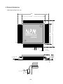
8. External dimensions ............................................................................................................................. I-45
II. I/O device (G9002) ...................................................................................................II-1
1. Outline ................................................................................................................................................... II-3
2. Features................................................................................................................................................. II-3
3. Basic specifications ............................................................................................................................... II-3
3-1. I/O device specifications (G9002) ................................................................................................. II-3
4. Hardware Description ............................................................................................................................ II-4
4-1. List of terminals (QFP-80) ............................................................................................................. II-4
4-2. Terminal assignment drawings ...................................................................................................... II-6
4-3. Complete block diagram................................................................................................................ II-7
4-4. Functions of terminals ................................................................................................................... II-8
4-4-1. CLK ......................................................................................................................................... II-8
4-4-2. #RST ....................................................................................................................................... II-8
4-4-3. CKSL....................................................................................................................................... II-8
4-4-4. #DN0 to #DN5......................................................................................................................... II-8
4-4-5. DNSM...................................................................................................................................... II-9
4-4-6. #DNSO.................................................................................................................................... II-9
4-4-7. SPD0, SPD1 ........................................................................................................................... II-9
4-4-8. TUD ......................................................................................................................................... II-9
4-4-9. TMD......................................................................................................................................... II-9
4-4-10. #TOUT ................................................................................................................................ II-10
4-4-11. SO ....................................................................................................................................... II-10
4-4-12. SOEH, #SOEL .................................................................................................................... II-10
4-4-13. SOEI.................................................................................................................................... II-10
4-4-14. SI......................................................................................................................................... II-10
4-4-15. #MRER................................................................................................................................ II-10
4-4-16. #MSEL ................................................................................................................................ II-10
4-4-17. BRK..................................................................................................................................... II-10
4-4-18. PMD0 to PMD2 ....................................................................................................................II-11
4-4-19. #P0N, #P1N, #P2N, #P3N ...................................................................................................II-11
4-4-20. P00 to 07, P10 to 17, P20 to 27, P30 to 37 .........................................................................II-11
4-5. Status after reset ..........................................................................................................................II-11
5. Electrical Characteristics ..................................................................................................................... II-12
5-1. Absolute maximum ratings .......................................................................................................... II-12
5-2. Recommended operating conditions........................................................................................... II-12
5-3. DC characteristics ....................................................................................................................... II-12
5-4. AC characteristics........................................................................................................................ II-13
5-4-1. System clock ......................................................................................................................... II-13
5-4-2. Reset timing .......................................................................................................................... II-13
5-4-3. Fixed output data timing........................................................................................................ II-14
5-4-4. Input data set timing.............................................................................................................. II-14
6. External dimensions ............................................................................................................................ II-15
III. Connection Examples and Recommended Environments......................................III-1
1. Connection examples ........................................................................................................................... III-3
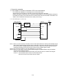
1-1. An example of a circuit to interface a CPU to a center device ..................................................... III-3
1-1-1. I/F mode 4 (IF1 = H, IF0 = H)................................................................................................. III-3
1-1-2. I/F mode 3 (IF1 = H, IF0 = L) ................................................................................................. III-4
1-1-3. I/F mode 3 (IF1 = L, IF0 = H) ................................................................................................. III-5
1-1-4. I/F mode 1 (IF1 = L, IF0 = L).................................................................................................. III-6
1-1-5. Connecting to a CPU without a wait function......................................................................... III-7
1-2. Access timing................................................................................................................................ III-8
1-2-1. Normal access ....................................................................................................................... III-8
1-2-1-1. Write to the I/O buffer or the data transfer FIFO............................................................... III-8
1-2-1-2. Writing to a memory address............................................................................................ III-9
1-2-1-3. Read timing....................................................................................................................... III-9
1-2-2. Access by commands .......................................................................................................... III-10
1-2-2-1. Write operation command............................................................................................... III-10
1-2-2-2. Write data to memory using write commands .................................................................III-11
1-2-2-3. Read data from memory using read commands ............................................................ III-12
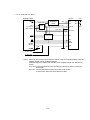
1-3. Line transceiver and pulse transformer for the center device .................................................... III-13
1-4. Line transceivers and pulse transformers for local devices ....................................................... III-14
1-5. A connection example of a level shifter ...................................................................................... III-16
1-6. Complete configuration............................................................................................................... III-17
2. Recommended environment .............................................................................................................. III-18
2-1. Cable .......................................................................................................................................... III-18
2-2. Terminating resistor .................................................................................................................... III-18
2-3. Pulse transformer ....................................................................................................................... III-18
2-4. I/F chip ........................................................................................................................................ III-18
2-5. Parts used in our experiments.................................................................................................... III-19
2-6. Other precautions ....................................................................................................................... III-19
IV. Software Examples (flow chart) ..............................................................................IV-1
1. Assumption ........................................................................................................................................... IV-3
1-1. Environment and precautions used for the descriptions .............................................................. IV-3
1-2. Commands used .......................................................................................................................... IV-3
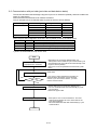
2. Software Examples............................................................................................................................... IV-4
2-1. Start of the simplest cyclic communication................................................................................... IV-4
2-2. The center device specifies the data for the local devices that are connected ............................ IV-5
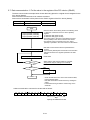
2-3. Set up an input-change interrupt .................................................................................................. IV-7
2-4. Check and clear any existing input-change interrupts ................................................................. IV-9
2-5. Check and clear cyclic communication errors ............................................................................ IV-11
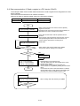
2-6. Communication with port data (port data and data device status) ............................................. IV-13
2-7. Data communication 1: Put the value in the register of the PCL device (G9x03) ...................... IV-15
2-8. Data communication 2: Read a register in a PCL device (G9x03)............................................. IV-16
2-9. Data communication 3: Start the PCL device (G9x03)............................................................... IV-17
2-10. Data communication 4: Start a PCL6045B using a CPU emulation device ............................. IV-19
2-11. An example of measuring when a break occurs....................................................................... IV-23
V. Troubleshooting ........................................................................................................V-1
1. Checking the center device ................................................................................................................... V-1
2. Checking the local devices .................................................................................................................... V-1
3. Checking the system ............................................................................................................................. V-1
VI. Handling Precautions ............................................................................................ VI-1
1. Design precautions ............................................................................................................................... VI-1
2. Precautions for transporting and storing LSIs ...................................................................................... VI-1
3. Precautions for mounting...................................................................................................................... VI-2
3-1. About the center device (G9001A) ............................................................................................... VI-2
3-2. I/O device (G9002) ....................................................................................................................... VI-3
4. Other precautions ................................................................................................................................. VI-4
VII. Differences between the G9001 and G9001A ..................................................... VII-1
1. How to distinguish between the G9001 and G9001A using a program............................................... VII-1
2. Newly added functions in the G9001A ................................................................................................ VII-1
2-1. Main status .................................................................................................................................. VII-1
2-2. Operation commands .................................................................................................................. VII-1
2-3. Register access command .......................................................................................................... VII-2
2-4. Register ....................................................................................................................................... VII-2
2-4-1. RENV0 register ..................................................................................................................... VII-2
2-4-2. RERCNT ............................................................................................................................... VII-3
2-4-3. RSYCNT ............................................................................................................................... VII-3
2-4-4. RDJADD................................................................................................................................ VII-3
2-4-5. RVER .................................................................................................................................... VII-3
I. Center device (G9001A)
User's Manual
I-1
I-2
1. Outline
This LSI is a center device of the Motionnet system.
It contains 256-byte RAM for controlling I/O and 512-byte RAM for data communication, and can control up to
64 local devices.
The local devices can be classified into I/O devices (G9002) that control input/output signals such as
G8014C on the T-NET system, and data device (G9x03, G9004A) that control by data such as G8015. It
allocates device numbers from 0 to 63 for each local device.
One I/O device (G9002) has 4 ports (1 port = 8 bits) for input/output (select input/output by terminals).
Therefore, connecting all the local devices to the center device as I/O device(G9002), you can connect I/Os
of 2048 points (64 units x 4 ports x 8 bits = 2048) by serial communication.
One data device (G9x03 or G9004A) can communicate max. 256 bytes data (maximum data length of the
PCL device (G9x03) will be 8 byte communication).
Suppose that all of the local devices connected to the center device as PCL devices (G9x03), 64 axes can be
controlled by serial communication.
2. Features
- Maximum data transfer speed is 20 Mbps.
- Transfer cycle time is less than 1 msec when 64 local devices are connected (in case of cyclic
communication only).
- One center device can connect up to 256 ports (2048 bits) for I/O connection.
- The center device provides input interrupt function to a CPU.
- Local devices are classified into the following devices:
* "I/O device" dedicated to control I/O port (G9002)
* "PCL device" to generate pulse strings.(G9x03)
* "CPU emulation device" to control data communication between CPUs and other peripheral
equipment.(G9004A)
- Local devices are allocated device numbers (0 to 63) with hardware. These device numbers can be
assigned at random in a Motionnet system. Further, by system communication, device numbers can
automatically be allocated.
- The center device is integrated with a memory for I/O ports. Thus, the center device can operate I/O status
just like accessing normal memories.
- The center device is integrated with four types of CPU-I/F circuits (Z80, 8086, H8, 68000, etc.). As it applies
for typical CPU interfaces, it will offer wide possibility to interface with a variety of CPUs.
- The center device normally uses 512 bytes area as address area. However, if resource is shorted, it can
use 8-byte areas.
- Input 3.3 V single power as power supply.
However, the major terminals can be connected to devices that run with 5 V.
I-3
3. General specifications
3-1. Communication system specifications
Item
Description
Reference clock
Note 1 40 MHz or 80 MHz
Communication speed Note 2 2.5 M, 5 M, 10 M, or 20 Mbps
Communication sign
NRZ sign
Communication protocol
NPM original method
Communication method
Half-duplex communication
Communication I/F
Note 3 RS-485 or pulse transfer
Connection method
Multi-drop connection
Number of local devices
64 devices max.
Cyclic communication cycle
When using 8 local devices
when 20 Mbps
(IN: 128 points, OUT: 128 points) --- 0.12 msec.
Note 4 When using 16 local devices
(IN: 256 points, OUT:256 points) --- 0.24 msec.
When using 32 local devices
(IN: 512 points, OUT: 512 points) --- 0.49 msec.
When using 64 local devices
(IN: 1024 points, OUT: 1024 points) --- 0.97 msec.
Note 1: When transferring data with 20 Mbps speed, and if the clock duty can be maintained to ideal "50:50"
condition, the center device can be operated by inputting 40 MHz clock signal.
The above ideal conditions mean that an oscillator and the center device are connected as 1:1 and
close to each other. (Actually, even these conditions cannot establish 50:50. However, a duty
approximate to the ideal one will be established.
Even if the ideal duty is broken a little, when signal lines are shorter and/or the number of local
devices is smaller, the center device can operate without any trouble. (For the details, see the
section for the "CLK" terminal.)
When the signal lines are longer and/or the number of connected local devices is greater and if it is
difficult to warranty the clock duty, you should take measures such as preparing an 80 MHz signal
or preparing a 40 MHz clock proprietary to the center device.
To select clock rate, specify using the LSI terminal. In either clock rate, the maximum speed of 20
Mbps is the same.
Note 2: Select the communication speed using the LSI terminal. Regardless of the selection of the
communication speed, the reference clock remains the same.
Note 3: NPM recommends using a system with a pulse transformer.
Note 4: The number of I/O ports in the parenthesis is true when the all the connected local devices are
connected as I/O device (G9002).
When data devices are connected such as PCL device (G9x03), the number of available I/O points
will be decreased. However, basic cyclic cycle (alt. frequency) does not change. (When the center
device communicates data, the frequency will be changed. For this matter, see the "Calculation of
communication time" in this manual.
I-4
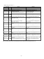
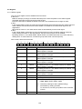
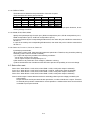
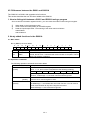
3-2. Center device specifications (G9001A)
Item
Address area
Address map
Description
Normally it uses 512 bytes area (A0 to A8).
However, 8 bytes area (A0 to A2) can be used when using the I/O buffer
(Note).
Address (h)
000 to 001
002 to 003
004 to 005
006 to 007
008 to 077
078 to 0B7
0B8 to 0BF
0C0 to 0DF
0E0 to 0FF
100 to 1FF
Communication
data length
Data
communication
time
CPU-I/F
Transfer method
Package
Power source
Storage
temperature range
Operating
temperature range
Writing
Command
Invalid
I/O buffer
Data sending FIFO
Not specified (112 bytes)
Reading
Status
Interrupt status
I/O buffer
Data receiving FIFO
Not specified (112
bytes)
Device information (8 bits / Device information (8
device)
bits / device)
Reset cyclic
Cyclic communication
communication error flag
error flag
Set input port change
Set input port change
interrupt
interrupt
Reset input port change
Input port change
interrupt flag
interrupt flag
I/O port data
I/O port data
1 to 128 word/frame (1 word = 16 bits)
When communicating 3 words (write 1 register of PCL) --- 19.3 s
When communicating 128 words --- 168.1 s
Integrated 4 types of CPU-I/F circuit (Z80, 8086, H8, 68000 etc.)
Cyclic transfer for I/O port, transit transfer for data communication
64-pin QFP (model section: 10 x 10 x 1.4 mm)
3.3 V±10%
-65 to +150oC
-40 to +85oC
Note: By issuing an operation command to the center device, you can access the entire address area
through a single I/O buffer. (It will take more time than direct access.)
Required address area is only 8-bytes (3 address signals).
For concrete use example, see the software examples in chapter IV.
I-5
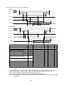
4. Hardware description
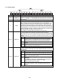
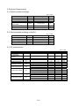
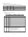
4-1. A list of terminals (QFP-64)
Signal name
I/O
1
IFO
I
2
IF1
I
3
#CS
I
4
#WR
I
5
#RD
I
6
A0
I
7
A1
I
8
A2
I
9
A3
I
10 GND
I
11 A4
I
12 A5
I
13 A6
I
14 A7
I
15 A8
I
16 VDD
I
17 D0
B
18 D1
B
19 D2
B
20 D3
B
21 GND
I
22 D4
B
23 D5
B
24 D6
B
25 D7
B
26 VDD
I
27 D8
B
28 D9
B
29 D10
B
30 D11
B
31 GND
I
32 D12
B
33 D13
B
34 D14
B
35 D15
B
36 VDD
I
37 #INT
O
38 #WRQ
O
39 #IFB
O
40 #MCRY
O
Logic
Negative
Negative
Negative
Positive
Positive
Positive
Positive
Positive
Positive
Positive
Positive
Positive
Positive
Positive
Positive
Positive
Positive
Positive
Positive
Positive
Positive
Positive
Positive
Positive
Positive
Positive
Positive
Positive
Negative
Negative
Negative
Negative
41
#MERR
O
Negative
42
43
GND
#MERF
O
O
Negative
44
45
MSYN
#SOEL
O
O
Negative
Negative
Description
CPU-I/F mode setting bit 0
CPU-I/F mode setting bit 1
Select chip
Write
Read
Address bus bit 0 (LSB)
Address bus bit 1
Address bus bit 2
Address bus bit 3
GND
Address bus bit 4
Address bus bit 5
Address bus bit 6
Address bus bit 7
Address bus bit 8
+3.3 V power input
Data bus bit 0 (LSB)
Data bus bit 1
Data bus bit 2
Data bus bit 3
GND
Data bus bit 4
Data bus bit 5
Data bus bit 6
Data bus bit 7
+3.3 V power input
Data bus bit 8
Data bus bit 9
Data bus bit 10
Data bus bit 11
GND
Data bus bit 12
Data bus bit 13
Data bus bit 14
Data bus bit 15
+3.3 V power input
Interrupt request
Wait request
CPU-I/F is busy
By detecting a communication line
signal, this signal becomes L for a rated
interval.
When received an error frame and no
response, this signal becomes L level for
a rated interval.
GND
When receiving an error response frame,
this signal becomes L level for a rated
interval.
The level reverses at each cyclic cycle.
Enable serial output
I-6
5V interface
Available
Available
Available
Available
Available
Available
Available
Available
Available
Available
Available
Available
Available
Available
Available
Available
Available
Available
Available
Available
Available
Available
Available
Available
Available
Available
Available
Available
Available
Available
Available
Available
Available
Available
Available
Available
Available
46
47
48
49
50
51
52
53
54
55
56
57
58
59
60
61
62
63
64
Signal name
SOEH
SO
VDD
SPD0
SPD1
SIA
GND
VDD
SIB
GND
CKSL
GND
CLK
VDD
GND
GND
GND
#RST
VDD
I/O
O
O
I
I
I
I
I
I
I
I
I
I
I
I
I
I
I
I
I
Logic
Positive
Positive
Positive
Positive
-
Negative
Description
Enable serial output
Serial output
+3.3 V power input
Communication speed setting bit 0
Communication speed setting bit 1
Serial input A
GND
+3.3 V power input
Serial input B
GND
Clock selection (L: 40 MHz, H: 80 MHz)
GND
Reference clock
+3.3 V power input
GND
GND
GND
Reset
+3.3 V power input
5V interface
Available
Available
Available
Note 1: "I" in the I/O column is for input, "O" is output, and "B" is both directions.
Note 2: As for the terminals with "available" in the 5V interface column, note the following.
* These terminals can be input at 5 V level signal. These are deleted diodes for overcurrent
protection on 3.3 V lines. If over voltage may be possible to charge due to reflection, linking, or
inductive noise, we recommend inserting a diode for overcurrent protection.
* Outputs from 5V devices can be connected to the center device as far as these are TTL level.
(Even if a signal is pulled up to 5V, the output level will be less than 3.3 V.) However, CMOS
level signals cannot be connected.
* On the CPU bus interface, pull up of 5 V level is possible for stabilizing bus lines (prevent
floating). Use 10 k-ohm or larger capacity pull up resistors.
I-7
VDD
SO
SOEH
#SOEL
MSYN
#MERF
GND
#MERR
#MCRY
#IFB
#WRQ
#INT
VDD
D15
D14
D13
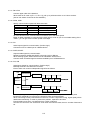
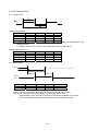
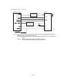
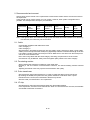
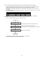
4-2. Terminal allocation diagram
48
47
46
45
44
43
42
41
40
39
38
37
36
35
34
33
SPD0 49
32
D12
SPD1 50
31
GND
SIA 51
30
D11
GND 52
29
D10
VDD 53
28
D9
SIB 54
27
D8
GND 55
26
VDD
CKSL 56
25
D7
24
D6
23
D5
22
D4
21
GND
20
D3
GND 62
19
D2
#RST 63
18
D1
VDD 64
17
D0
6
7
IF1
#CS
#WR
#RD
A0
A1
8
9
10
11
12
13
14
15
16
VDD
5
A8
4
A7
3
A6
2
A5
1
IF0
GND 61
A4
GND 60
GND
VDD 59
A3
CLK 58
A2
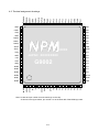
G9001A
XXXXXXXXX
JAPAN
GND 57
Note: For each pin number, see the marks on the actual LSI.
As shown above, to the lower left of the NPM logo mark is the 1st pin.
I-8
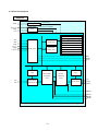
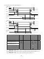
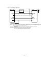
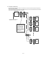
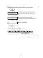
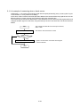
4-3. Entire block diagram
G9001A
#RST
SPD (1:0)
CKSL
Reset control circuit
Internal reset
Clock control
Internal clock (20 MHz)
circuit
Internal clock (40 MHz)
CLK
Memory area
Device information area
Memory area
control circuit
#CS
#RD
Cyclic communication error flag
Input change interrupt setting area
Input change interrupt flag area
#WR
Port 0 data area
IF (1:0)
A (8:0)
D (15:0)
Command
CPU I/F circuit
Port 1 data area
control circuit
Port 2 data area
Port 3 data area
#INT
#WRQ
#IFB
Data receiving
Data transfer
FIFO
FIFO
SIA
Serial signal
SIB
receiving circuit
Receipt data
Transfer
processing
processing
circuit
circuit
Serial signal
transfer circuit
SO
SOEH
#SOEL
#MSYN
#MCRY
#MERR
#MERF
I-9
4-4. Functions of terminals
4-4-1. CLK
This is an input terminal of the reference clock. By setting of the CKSL terminal, either of the following
clock rate signals can be connected.
CKSL = L: 40 MHz
CKSL = H: 80 MHz
By selecting either of these clock rates, the serial communication transfer rate does not change. This
clock rate selection affects communication precision.
For a small-scale serial communication and transfer rate below 10 Mbps, use of the center device with 40
MHz does not give any restriction.
With 20 Mbps transfer speed; however, longer communication lines or a large number of connected local
devices may deteriorate communication precision due to collapse of signals on the circuit. This
deterioration of communication quality can be corrected inside the LSI, if the deterioration level is not
much. In order to improve correction precision; however, evenness of the clock duty is required. In other
words, if the duty is ideal (50:50), the capacity to correct collapse of the signals in the communication lines
can be improved. On the contrary, if the duty is not ideal, the center device cannot cope with collapses of
the communication line.
As a result, if the duty is close to ideal, the center device can be used with 40 MHz. When connecting
more than one oscillator, the duty will not be ideal. In this case, select 80 MHz. The center device divides
the frequency inside and creates 40 MHz frequency.
If you do not want 80 MHz frequency, you may prepare a separate 40 MHz oscillator for this LSI.
4-4-2. #RST
This is an input terminal for a reset signal.
By inputting an L level signal, the center device is reset. As the center device synchronizes with a clock,
arrange a circuit so that it does not disconnect the clock while resetting. Reset signal length longer than
10 clock cycles is required.
4-4-3. CKSL
Use to select clock rate.
L: Connect 40 MHz clock frequency to the CLK terminal.
H: Connect 80 MHz clock frequency to the CLK terminal.
Select this when the duty of the 40 MHz clock collapses too much.
I-10
4-4-4. IF0, IF1
Specify CPU-I/F mode
Set status
IF1
IF0
L
L
H
H
L
H
L
H
I/F mode
I/F mode 1
I/F mode 2
I/F mode 3
I/F mode 4
CPU signal to connect to terminals
#RD
#WR
A0
#WRQ
terminal
terminal
terminal
terminal
(VDD)
R/W
#LDS
#DTACK
#RD
#HWR
(VDD)
#WAIT
#RD
#WR
(GND)
READY
#RD
#WR
A0
#WAIT
Example
of CPU
68000
H8
8086
Z80
This LSI has the following four interface modes.
The above four CPUs are typical ones among CPUs currently available on the market. Even if a CPU you
are examining is other than the above CPUs, most of the CPUs can be connected using either of the
interfaces above. For details, see the hardware specification sheets of the CPU you are planning to use,
and check with which mode you can connect.
Note: The classification of the CPU interface modes above is applicable only for the center device. The
CPU emulation device G9004A also has unique CPU interface modes. Mode classification of this is
different than the above.
4-4-5. #CS
Input L level signal to this terminal when accessing this LSI.
4-4-6. #RD, #WR, A0, and #WRQ
Connect I/F signals with a CPU. Input signals vary with setting of the IF0 to 1.
For the details, see items "IF0 and IF1."
4-4-7. #INT
Outputs an interrupt request signal.
When not using this terminal, keep this terminal open.
4-4-8. #IFB
Use this terminal when connecting with a CPU having no wait control input terminal.
By reading a command from a CPU, this signal becomes L level. When the command process is complete,
this signal returns to H level. After confirming that this terminal is H level, access the center device.
4-4-9. A1 to A8
Enter address signal to these terminals.
When the IF1 is L, address bus A1 to A8 are inverted inside.
When to control at 8-byte area, process as follows:
IF1 terminal status
L
H
A (8:3) process
Pull up (set to H)
GND (set to L)
4-4-10. D0 to D7
Connect lower 8 bits of the data bus.
I-11
Remarks
I/F mode 1, 2
I/F mode 3, 4
4-4-11. D8 to D15
Connect upper 8 bits of the data bus.
When used as I/F mode 4 (IF1 = H, IF0 = H), pull up or pull down with 5 to 10 K-ohms resistor.
(Use of one resistor for 8 lines is also available.)
4-4-12. SPD0, SPD1
Specify communication speed with these terminals.
SPD1
SPD0
Communication speed
L
L
2.5 Mbps
L
H
5 Mbps
H
L
10 Mbps
H
H
20 Mbps
All of the devices on the communication line shall be set to the same speed.
Either 40 MHz or 80 MHz is connected to the clock signal, as far as you do not mistake setting of the
"CKSL," you can get communication speed of 20 Mbps.
4-4-13. SO
Serial output signal for communication. (Positive logic)
Connect this line to a data input of a RS485 device.
4-4-14. SOEH, #SOEL
Output enable signal for communication.
Difference between SOEH and #SOEL is that only logic is different.
When sending signals, SOEH will become H and #SOEL will become L.
Connect either of needed signal to the data enabled input of a RS485 device.
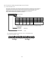
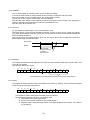
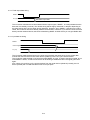
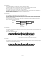
4-4-15. SIA, SIB
Serial input signals for communication. (Positive logic)
Basically these two are identical in functions.
Each of them can construct independent signal line as follows.
SIA
Center
device
SIB
Line
Transceiver
Transformer
Local
device
SO
Line
Transceiver
Local Local
device device
Transformer
Local Local Local
device device device
Commonly using the serial output signal "SO" from the center device, provide RS485 and pulse
transformer individually for each line, the signal line load can be decreased.
When connecting to many local devices on one line, or when a signal line is long, signal quality will be
deteriorated remarkably. In order to prevent this problem, separate to two lines.
Even divided into two lines, use easiness from a CPU is identical.
One line can connect to max. 64 devices. Even when two lines are used, the max. number of devices is
64.
I-12
4-4-16. #MCRY
This is a monitor output to confirm communication.
When a signal is transferred on the signal line, this terminal outputs L signal. If there is no signal on the
signal line, this terminal outputs H signal.
4-4-17. #MERR
This is a monitor output to check communication quality.
When the center device receives an error frame such as a CRC error, or when it cannot receive a
response frame within 20 s, the signal becomes L only for 128 cycles (3.2 s) of the CLK.
By measuring the condition using the counter, you can check communication quality.
4-4-18. #MERF
This is a monitor terminal to confirm communication control status.
When the center device receives an error response frame, this terminal outputs L level signal only for
0.2 seconds.
The error response frame is as follows:
A local device normally receives signals from the center device if there is no CRC error on the local
device.
However, it may possible that the received data do not match with the local device status (such as
receiving output data on the input port).
In this case, the local device sends back the data to the center device in order to notify the center device
that the received data is useless.
This is error response frame.
Other case is that a local device sends data longer than 8 bytes to a PCL device (G9x03 8 bytes FIFO),
and the PCL device returns receipt process error (format error).
4-4-19. MSYN
This is a monitor output of cyclic communication cycle.
Each time a cyclic communication cycle ends, this signal level changes between L and H.
I-13
4-5. Address map
Address map (1) I/F mode 4 (Please be aware of Notes 1 and 2 while accessing)
A0 to A8
0 0000 0000
0 0000 0001
0 0000 0010
0 0000 0011
0 0000 0100
0 0000 0101
0 0000 0110
0 0000 0111
0 0000 1000
|
0 0111 0111
0 0111 1000
0 0111 1001
000h
001h
002h
003h
004h
005h
006h
007h
008h
|
077h
078h
079h
|
|
0 1011 0110
0 1011 0111
0 1011 1000
0B6h
0B7h
0B8h
0 1011 1001
0B9h
|
|
0 1011 1110
0BEh
0 1011 1111
0BFh
0 1100 0000
0C0h
0 1100 0001
0C1h
|
Writing
Command bits 0 to 7
Command bits 8 to 15
Invalid
Invalid
Input/output buffer bits 0 to 7
Input/output buffer bits 8 to 15
Data transfer FIFO bits 0 to 7
Data transfer FIFO bit 8 to 15
Reading
Note 1 Status bits 0 to 7
Note 1 Status bits 8 to 15
Interrupt status bits 0 to 7
Interrupt status bits 8 to 15
Input/output buffer bits 0 to 7
Input/output buffer bits 8 to 15
Note 1 Data receiving FIFO bits 0 to 7
Note 1 Data receiving FIFO bits 8 to 15
Not defined (112 bytes)
(Any data written here will be ignored.)
Not defined (112 bytes)
(Always read as 00h.)
Device information (Device No. 0)
Device information (Device No. 1)
Device information (Device No.0)
Device information (Device No.1)
|
Note 2
Note 2
|
Device information (Device No. 62)
Device information (Device No. 63)
Cyclic communication error flags
(Device No. 0 to 7)
Cyclic communication error flags
(Device No. 8 to 15)
|
Device information (Device No.62)
Device information (Device No.63)
Cyclic communication error flags (Device
No. 0 to 7)
Cyclic communication error flags (Device
No. 8 to 15)
|
Cyclic communication error flags
(Device No. 48 to 55)
Cyclic communication error flags
(Device No. 56 to 63)
Input change interrupt settings (Device
No. 0, 1)
Input change interrupt settings (Device
No. 2, 3)
Cyclic communication error flags (Device
No. 48 to 55)
Cyclic communication error flags (Device
No. 56 to 63)
Input change interrupt settings (Device
No. 0 to 1)
Input change interrupt settings (Device
No. 2, 3)
|
|
|
0 1101 1110
0DEh
0 1101 1111
0DFh
0 1110 0000
0E0h
0 1110 0001
0E1h
Input change interrupt settings (Device
No. 60, 61)
Input change interrupt settings (Device
No. 62, 63)
Input change interrupt flags (Device No.
0, 1)
Input change interrupt flags (Device No.
2, 3)
Input change interrupt settings (Device
No. 60, 61)
Input change interrupt settings (Device
No. 62, 63)
Input change interrupt flags (Device No.
0, 1)
Input change interrupt flags (Device No.
2, 3)
|
|
|
0 1111 1110
0FEh
0 1111 1111
0FFh
1 0000 0000
100h
Input change interrupt flags (Device No.
60, 61)
Input change interrupt flags (Device No.
62, 63)
Port data No. 0 (Device No.0 - Port 0)
Input change interrupt flags (Device No.
60, 61)
Input change interrupt flags (Device No.
62, 63)
Port data No. 0 (Device No.0 - Port 0)
|
I-14
A0 to A8
1 0000 0001
101h
1 0000 0010
102h
1 0000 0011
103h
|
1 1111 1100
1 1111 1101
1 1111 1110
1 1111 1111
Writing
Port data No. 1 (Device No.0 - Port 1)
Port data No. 2 (Device No.0 - Port 2)
Port data No. 3 (Device No.0 - Port 3)
Reading
Port data No. 1 (Device No.0 - Port 1)
Port data No. 2 (Device No.0 - Port 2)
Port data No. 3 (Device No.0 - Port 3)
|
|
|
1FCh
1FDh
1FEh
1FFh
Port data No. 252 (Device No.63 - Port 0)
Port data No. 253 (Device No.63 - Port 1)
Port data No. 254 (Device No.63 - Port 2)
Port data No. 255 (Device No.63 - Port 3)
Port data No. 252 (Device No.63 - Port 0)
Port data No. 253 (Device No.63 - Port 1)
Port data No. 254 (Device No.63 - Port 2)
Port data No. 255 (Device No.63 - Port 3)
Note 1: Write in lower bit to upper bit order.
This order is especially important when accessing the FIFO used exclusively for sending data.
Note 2: Read in lower bit to upper bit order.
This order is especially important when accessing the FIFO used exclusively for receiving data.
I-15
Address map (2) I/F mode 3
A1 to A8
0 0000 000
000h
0 0000 001
002h
0 0000 010
004h
0 0000 011
006h
0 0000 100
008h
|
|
0 0111 011
076h
0 0111 100
078h
|
0 1011 011
0 1011 100
|
|
0B6h
0B8h
Writing
Command bits 0 to 15
Invalid
Input/output buffer bits 0 to 15
Data transfer FIFO bits 0 to 15
Reading
Status bits 0 to 15
Interrupt status bits 0 to 15
Input/output buffer bits 0 to 15
Data receiving FIFO bits 8 to 15
Not defined (56 words)
(Any data written here will be ignored.)
Not defined (56 words)
(Always read as 00h.)
Device information (Device No. 0, 1)
Device information (Device No.0, 1)
|
|
Device information (Device No. 62, 63)
Cyclic communication error flags
(Device No. 0 to 15)
Device information (Device No.62, 63)
Cyclic communication error flags (Device
No. 0 to 15)
|
|
|
0 1011 111
0BEh
0 1100 000
0C0h
Cyclic communication error flags
(Device No. 48 to 63)
Input change interrupt settings (Device No.
0 to 3)
Cyclic communication error flags (Device
No. 48 to 63)
Input change interrupt settings (Device No.
0 to 3)
|
|
|
0 1101 111
0DEh
0 1110 000
0E0h
Input change interrupt settings (Device No.
60 to 63)
Input change interrupt flags (Device No. 0
to 3)
Input change interrupt settings (Device No.
60 to 63)
Input change interrupt flags (Device No. 0
to 3)
|
|
|
0 1111 111
0FEh
1 0000 000
1 0000 001
100h
102h
Input change interrupt flags (Device No. 60
to 63)
Port data No. 0, 1 (Device No.0 - Port 0, 1)
Port data No. 2, 3 (Device No.0 - Port 2, 3)
Input change interrupt flags (Device No. 60
to 63)
Port data No. 0, 1 (Device No.0 - Port 0, 1)
Port data No. 2, 3 (Device No.0 - Port 2, 3)
|
|
|
|
|
|
1 1111 110
1FCh
1 1111 111
1FEh
Port data No. 252, 253 (Device No.63 Port data No. 252,253 (Device No.63 - Port
Port 0, 1)
0, 1)
Port No.254, 255 (Device No.63 - Port 2, 3) Port data No. 254, 255 (Device No.63 Port 2, 3)
Note: The hexadecimal notation for the addresses above are written with the assumption that A0 = 0.
I-16
Address map (3) I/F mode 1, 2
A1 to A8
1 1111 111
1FFh
1 1111 110
1FCh
1 1111 101
1FAh
1 1111 100
1F8h
1 1111 011
1F6h
|
|
1 1000 100
188h
1 1000 011
186h
|
1 0100 100
1 0100 011
|
|
148h
146h
Writing
Command bits 0 to 15
Invalid
Input/output buffer bits 0 to 15
Data transfer FIFO bits 0 to 15
Reading
Status bits 0 to 15
Interrupt status bits 0 to 15
Input/output buffer bits 0 to 15
Data receiving FIFO bits 8 to 15
Not defined (56 words)
(Any data written here will be ignored.)
Not defined (56 words)
(Always read as 00h.)
Device information (Device No. 0, 1)
Device information (Device No.0, 1)
|
|
Device information (Device No. 62, 63)
Cyclic communication error flags
(Device No. 0 to 15)
Device information (Device No.62, 63)
Cyclic communication error flags (Device
No. 0 to 15)
|
|
|
1 0100 000
140h
1 0011 111
13Eh
Cyclic communication error flags
(Device No. 48 to 63)
Input change interrupt settings (Device No.
0 to 3)
Cyclic communication error flags (Device
No. 48 to 63)
Input change interrupt settings (Device No.
0 to 3)
|
|
|
1 0010 000
120h
1 0001 111
11Eh
Input change interrupt settings (Device No.
60 to 63)
Input change interrupt flags (Device No. 0
to 3)
Input change interrupt settings (Device No.
60 to 63)
Input change interrupt flags (Device No. 0
to 3)
|
|
|
1 0000 000
100h
0 1111 111
0 1111 110
0FEh
0FCh
Input change interrupt flags (Device No. 60
to 63)
Port data No. 0, 1 (Device No.0 - Port 0, 1)
Port data No. 2, 3 (Device No.0 - Port 2, 3)
Input change interrupt flags (Device No. 60
to 63)
Port data No. 0, 1 (Device No.0 - Port 0, 1)
Port data No. 2, 3 (Device No.0 - Port 2, 3)
|
|
|
|
|
|
0 0000 001
002h
0 0000 000
000h
Port data No. 252, 253 (Device No.63 Port data No. 252,253 (Device No.63 - Port
Port 0, 1)
0, 1)
Port No.254, 255 (Device No.63 - Port 2, 3) Port data No. 254, 255 (Device No.63 Port 2, 3)
Note: The hexadecimal notation for the addresses above are written with the assumption that A0 = 0.
I-17
Note: The discussion of address maps below largely concerns I/F mode 3.
4-5-1. "Device information" area
With system communication, the center device polls all local devices, from device 0 to 63. According to
the response from local devices, the center device can confirm the connection status, device type,
settings for the I/O port on each local device, and refresh its own "device information" area.
When a CPU knows the "device information", the center device can write to it.
8 bits of device information are required for each device.
7 6 5 4 3 2 1 0
0 0 0
(Device information
I/O setting
Set value
Port0
Port1
Port2
Port3
PMD2 PMD1 PMD0
000
Output
Output
Output
Output
L
L
L
001
Input
Output
Output
Output
L
L
H
010
Input
Input
Output
Output
L
H
L
011
Input
Input
Input
Output
L
H
H
Other
than the
Input
Input
Input
Input
Other than the above
above
When a local device is a data device (G9x03, G9004A) , the port used to
exchange data (status or general-purpose ports) have a different meaning
for each device.
Device type
0: I/O device
1: Data device
Use of device
0: Do not use
1: Used
Ex.: To get device information for device Nos. 0 and 1, access address 078h.
For a 16-bit CPU (address = 078h)
I-18
4-5-2. "Cyclic communication area flags"
The center device communicates with all the I/O ports using cyclic communication.
In this type of cyclic communication, if a communication error occurs for a specific I/O device (G9002) on
three consecutive communication cycles, the center device will treat this as cyclic communication error.
When this error occurs, the bit in this area corresponding to the device number will become 1. By
checking these bits, you can identify the I/O device (G9002) in error.
Ex.: When reading address 0B8h
For a 16-bit CPU (address = 0B8h)
As seen above, the lowest bit shows the error status of the local device with the lowest address number.
By reading "0B8h," local device numbers from 0 to 15 can be checked. In the same way, by reading "BAh"
you can check device numbers 16 to 31.
To determine the address, proceed as follows. (discard any remainder)
Address = 0B8h + (Device No. / 8)
For an 8-bit CPU (Address = 0B8h)
The bits are read in groups of 8 by an 8-bit CPU, but the meaning of each bit is the same.
The device number refers to the number allocated to each local device. The numbers are specified on the
external terminals on local devices. Duplicate use of the same number is prohibited.
- To clear flags
In order to return a bit to 0 that was changed to a 1 when an error occurred, write a 1 to this bit.
The simplest way to clear a flag is to write the same data back to the same cyclic communication error flag
position that it was read from.
(For examples of how to use these flags, see point (2) in the "Check and Clear Errors" in "Software examples"
in Chapter IV.
I-19
4-5-3. "Change to Input Port Interrupt Setting" area
Port information for the I/O devices (G9002) that are connected can be obtained automatically using the
cyclic communication system. The center device also uses cyclic communication to periodically obtain
status information for the data devices (G9x03, G9004A) that are connected.
These changes to input ports and status changes in data devices can be detected automatically, and then
the center device can generate an interrupt (#INT) for a CPU.
This area can be addressed by writing bits that correspond to the local device number whose status you
want to monitor. When a bit is set to "1" its status will be monitored
Ex.: When you want to monitor port 2 on device number 0.
In order to specify device number 0, you have to access address 0C0h.
As shown above, there are 4 bits which correspond to each local device. The lowest 4 bits will be the
area for setting up interrupts for the local device with the lowest address number.
The lowest of the 4 bits corresponds to port 0, the next bit corresponds to port 1, and so forth.
When you want to monitor another local device, determine the address using the following rule
(discard any remainder).
Address = 0C0h + (device number / 2)
The rule is the same for an 8-bit CPU, except that the data will be transferred in units of 8 bits.
Since mainly status information corresponds to each port on data devices (G9x03, G9004A), you just
enter a "1" for the port which has the status you want to monitor.
For details, see "5-1-3. Input change interrupt" (Be especially careful when monitoring the status of a
device to make sure that port 0 is not monitoring all the bits.)
For details about which status information corresponds to which port, see the user's manual for each data
device (G9x03, G9004A).
(For examples of use, see point (2) in the "Set up an input-change interrupt" section of "Software
Examples" in Chapter IV.)
I-20
4-5-4. "Change-In-Input Interrupt Flag" area
If a port has been specified in the area for setting Change-In-Input Interrupts, when its port status changes,
the center device will issue an interrupt to a CPU and change the bit to a "1."
The interrupt allows the CPU to determine the device number and port number (or status) which changed
by reading this area.
Ex.: To monitor port 2 on device number 0
To read the status of device number 0 you must access address 0E0h.
4 bits correspond to each local device. The lower 4 bits are the Input Interrupt Setting area of the
local device with the lowest address number.
The lowest bit among these 4 corresponds to port 0, the next bit corresponds to port 1, and so
forth.
To check other local devices, specify the address by using the following rule (discard any
remainder).
Address = 0E0h + (device number / 2)
The procedure is the same for an 8-bit CPU, except that data will be handled in units of 8 bits.
- To clear flags
In order to return a bit to 0 that was changed to a 1 when a change occurred I the input, write a 1 to this bit.
The simplest way to clear a flag is to write the same data back to the same "input change interrupt flag" area
that it was read from.
(For examples of use, see point (2) in the "Change-In-Input Interrupt Setting" section of "Software Examples"
in Chapter IV.)
4-5-5. "Port data" area
This area is used primarily to set the data for output ports on I/O devices (G9002), and to check the data
from the input ports.
When the local device is a data device (G9x03, G9004A), this area is used to read status information and
set data for the general-purpose port (if any needs to be set).
To access this area, see the device number and port number described in the address map.
To learn which status register corresponds to which port when the local device is a data device (G9x03 or
G9004A), see the User's manual for each data device (G9x03, G9004A).
(For examples of use, see point (2) in the "Change-In-Input Interrupt Setting" section of "Software
Examples" in Chapter IV.)
I-21
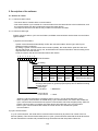
4-6. Status
STSW
STSB1
15
14
13
12
BBSY DBSY RBSY SBSY
Bit
Symbol
0
CEND
1
BRKF
2
IOPC
3
EIOE
4
EDTE
5
ERAE
6
CAER
7
(Not defined)
8
REF
9
TDBB
10
RDBB
11
12
(Not defined)
SBSY
11
STSB0
8
7
0 RDBB TDBB REF
10
9
0
6
5
4
3
2
1
0
CAER ERAE EDTE EIOE IOPC BRKF CEND
Description
Becomes 1 when ready for data to be written to the transmitting FIFO buffer.
When the system communication or data communication is complete and the next chunk of
data can be sent to the transmitting FIFO buffer, this bit becomes 1 and the center device
outputs an interrupt signal (#INT).
The method for clearing this bit will depend on status bit 9 in the RENV0 register.
When the center device receives a break frame this bit becomes 1 and an interrupt signal
(#INT) is output.
The method for clearing this bit will depend on status bit 9 in the RENV0 register
Becomes 1 when any input port which had enabled the input change interrupt setting and
that status changed. The center device then outputs an interrupt signal (#INT).
This signal is an OR of all 256 input port change interrupt flag bits.
When all the bits return to 0, this bit returns to 0.
Becomes 1 when a cyclic communication error occurs. The center device then outputs an
interrupt signal (#INT).
This signal is an OR of all 64 cyclic communication error flag bits.
For details about the conditions when the error occurred, see 1) cyclic communication error
in section 5-1-5.
When all the bits return to 0, this bit returns to 0.
Becomes 1 when a data communication error occurs. The center device then outputs an
interrupt signal (#INT).
For details about the conditions when the error occurred, see 2) Data communication error
in section 5-1-5.
The method for clearing this bit will depend on status bit 9 in the RENV0 register
Becomes 1 when a local device reception processing error occurs. The center device then
outputs an interrupt signal (#INT).
For details about the conditions when the error occurred, see the interrupt status CAE bit
description on the next page. Refer to this status bit to check which error occurred, the
device No. and other error details.
The method for clearing this bit will depend on status bit 9 in the RENV0 register
A CPU access error occurred.
When there is a problem accessing a CPU, such as a data send command being written
when there is no data to send, this bit becomes 1. The center device then outputs an
interrupt signal (#INT).
For details about the conditions when the error occurred, see the interrupt status ERA bit
description on the next page. Refer to this status bit to check which error occurred, the
device No. and other error details.
The method for clearing this bit will depend on status bit 9 in the RENV0 register..
Always 0.
When there is not-yet-sent output port data, this bit becomes 1.
When data is written to the output port this bit becomes 1. When the center device
successfully completes two rounds of cyclic communication to all the ports without any
errors, this bit will return to 0.
When there is data to send in the transmitting FIFO, this bit becomes 1.
After data is written to the transmitting FIFO, this bit becomes 1. Once a data send
command or a transmitting FIFO reset command is written, this bit returns to 0.
When data has been received in the receiving FIFO, this bit becomes 1.
When receiving data from a data device, this bit becomes 1. After a CPU has read all of the
data received, this bit returns to 0.
Always 0.
Becomes 1 when cyclic communication starts.
I-22
Bit
13
14
Symbol
RBSY
DBSY
15
BBSY
Description
Is 1 during a reset.
Is 1 during system communication or data communication.
When RENV0(8) is 1 and the center device issues a break communication command
(0610h), this bit stays 1 until the break communication is complete. This bit stays 0 for any
other case.
Note 1: When errors occur on more than one device, only the device number where the last error occurred
would be shown.
I-23
4-7. Interrupt status
Bit
Symbol
0 to 5
EDN0 to 5
6
(Not defined)
7
LNRV
8 to 11
ERA0 to 3
12 to 15
CAE0 to 3
Description
These bits show the number of the device which has an error, when
EDTE = 1 or ERAE = 1. These details are stored until the next time an
error occurs.
Always 0.
When a local device is not receiving data, this bit is 1.
When the data communication terminates with an error (EDTE = 1),
and if a local device cannot receive data from the center device (the
local device does not respond), this bit becomes 1. When the local
device has received the data (communication data from a local device
is interrupted by a communication error and the center device does not
receive the data normally, you have to check whether the local device
received the data normally), this bit returns to 0.
This condition is stored until the next time an error occurs.
These errors occur even if a local device received data normally but
the packet details of the data do not match at the local device.
When this error occurs, the center device will store one of the following
codes in these bits. This condition is stored until the next time an error
occurs.
Code Error conditions
0001
I/O setting information in the device information area in the
center device is not identical to the I/O port combination
(specified using the PMD terminal) on the local device.
0010
An I/O device(G9002) received a data communication
frame.
0011
A data device received frames larger than the receiving
buffer capacity of the data device.
If the CPU tries to access the G9001A illegally, it will store one of the
following codes in these bits. The code is stored until the next time an
error occurs.
Code Error conditions
0001
The CPU tried to write a cyclic communication start
command but the number of devices used was set to zero.
0010
Tried to write a start sending command without putting any
data in the data sending FIFO.
0011
While the DBSY = 1, a device tried to do one of the
following:
(1) Reading or writing to the transmitting or receiving FIFO.
(2) Wrote a system start command or a data
communication start command.
0100
Tried to communicate with a device which had device
information area bit 7 set to 0 (means the device is not
used).
I-24
4-8. Command
Note: Write to the 8-bit CPU I/F (IF0=H, IF1=1) in the following order: COMB0 then COMB1.
4-8-1. Operation command
Command
0000 0000 0000 0000
(0000h)
0000 0001 0000 0000
(0100h)
0000 0010 0000 0000
(0200h)
0000 0011 0000 0000
(00300h)
0001 0000 0$$$ 00$$
(04xxh)
Description
Invalid command
Resets the software.
Resets the center device. This is the same function as the #RST input.
Resets the transmitting FIFO.
Resets only the data transmitting FIFO.
Resets the receiving FIFO.
Resets only the data receiving FIFO.
Clear command for the INT group status.
Bits 0, 1, 4, 5, and 6 of the command have the following meaning.
0
CAER ERAE EDTE
0
0
BRKF CEND
By changing each of these bits, the corresponding status will be cleared.
However, if RENV0(9) = 0, the clear command will be ignored.
0000 0110 0000 0000 Error count clear command.
(0600h) Clear the error counter register to zero.
0000 0110 0001 0000 Break communication command.
(0610h) Set RENV0(8) = 1 and disable the auto break function. You can issue a break
communication at any time using this command.
When REIV0(8) = 0, this command is ignored.
Note: For all bits marked with a #, the upper bits of the device address should be set in order, starting from the
left end of the # bits.
For bits with marked with an &, when the port is 0 or 1, set the bit to 0. When the port is 2 or 3, set the bit
to 1.
Either 0 or 1 may be used for bits marked with a $.
For bits marked with an x, either 0 or 1 may be used.
I-25
Command
0001 0000 0000 0000
(1000h)
Description
System communication to all devices.
Polls all of the devices (device Nos. 0 to 63) one by one, and refreshes the
device information areas that correspond to each device number.
The device information contains the following:
- Device in use: 0 when no response, and 1 when it responds.
- Device type: Reset to 1 when it is a data device.
- I/O setting information
No response to a system communication is not treated an error. However,
an error with a CRC mismatch may be possible.
0001 0001 0000 0000 System communication to all devices except those devices excluded from
(1100h)
cyclic communication.
After checking the device information area, the center device polls all the
devices whose device-in-use bit is set to 0, one by one, and refreshes the
device information areas that correspond to each device number.
The details are refreshed the same as by writing a command 1000h.
No response to a system communication is not treated an error. However,
an error with a CRC mismatch may be possible.
0001 0010 00## #### System communication to specified devices.
(1200h to 123Fh)
The center device polls only the specified devices and refreshes the
device information areas that correspond to each specified device
number.
The details are refreshed the same as by writing a command 1000h.
No response to a system communication is not treated an error. However,
an error with a CRC mismatch may be possible.
0001 0011 00## ####
Obtain attribute information for the specified devices.
(1300h to 133Fh)
The polling response frame consists of device attribute information. This
command polls the specified devices and copies the attribute information
into the data receiving FIFO.
The device information area does not change.
The details of the data receiving FIFO are as follows.
Bits 0 to 4: (Number of bytes for the longest piece of data) / 8 -1
Bits 5 to 7: Not used (not defined)
Bits 8 to 15: Device type code (I/O device: 01h, Data device: 81h)
Bits 16 to 18: Set the I/O port (PMD terminal information when an I/O
device is selected)
Bit 19: Always 0
Bits 20 to 31: Data device type (G9003:000h,G9004A:001h,G9103:002h)
0011 0000 0000 0000
Start cyclic communication
(3000h)
Start cyclic communication with devices that have a 1 in the device-in-use
bit in the device information.
0011 0001 0000 0000
Stop cyclic communication.
(3100h)
Stop the current cyclic communication.
0100 0000 00## ####
Data communication.
(4000h to 403Fh)
Sends data in the transmitting FIFO to the specified devices. The data
received in response will be stored in the receiving FIFO.
0100 0001 0000 0000
Cancel data communication
(4100h)
Halt the data communication and reset the transmitting FIFO.
This command will be ignored after the data has been sent.
Note: For all bits marked with a "#," the upper bits of the device address should be set in order, starting from
the left end of the # bits.
For bits marked with an "&," when the port is 0 or 1, set the bit to 0. When the port is 2 or 3, set the bit
to 1.
For bits marked an "x," either 0 or 1 may be used.
G9002: I/O device
G9x03: PCL device
G9004A: CPU emulation device
I-26
Command
0101 0001 0##x xxxx
(5100h to 517Fh)
Description
Write to the "cyclic communication error flag" area.
The contents of the I/O buffer are written into a word in this area.
Use this function when you want to reduce the number of addresses
used in this device.
0101 0010 0### #xxx
Write to the "input change interrupt setting" area.
(5200h to 527Fh) The contents of the I/O buffer are written into a word in this area.
Use this function when you want to reduce the number of addresses
used in this device.
0101 0011 0### #xxx
Write to the "input change interrupt flag" area.
(5300h to 537Fh) The contents of the I/O buffer are written into a word in this area.
Use this function when you want to reduce the number of addresses
used in this device.
0101 0100 0### ###& Write to the "port data" area.
(5400h to 547Fh) The contents of the I/O buffer are written into a word in this area.
Use this function when you want to reduce the number of addresses
used in this device.
0110 0000 0### ##xx
Read the "device information" area.
(6000h to 607Fh) The contents of the word in this area are copied to the I/O buffer.
Use this function when you want to reduce the number of addresses
used in this device.
0110 0001 0##x xxxx
Read the "cyclic communication error flag" area.
(6100h to 617Fh) The contents of the word in this area are copied to the I/O buffer.
Use this function when you want to reduce the number of addresses
used in this device.
0110 0010 0### #xxx
Read the "input change interrupt setting" area.
(6200h to 627Fh) The contents of the word in this area are copied to the I/O buffer.
Use this function when you want to reduce the number of addresses
used in this device.
0110 0 11 0### #xxx
Read the "input change interrupt flag" area.
(6300h to 637Fh) The contents of the word in this area are copied to the I/O buffer.
Use this function when you want to reduce the number of addresses
used in this device.
0110 0100 0### ###& Read the "port data" area.
(6400h to 647Fh) The contents of the word in this area are copied to the I/O buffer.
Use this function when you want to reduce the number of addresses
used in this device.
Note: For all bits marked with a "#," the upper bits of the device address should be set in order,
starting from the left end of the # bits.
For bits marked with an "&," when the port is 0 or 1, set the bit to 0. When the port is 2 or 3,
set the bit to 1.
For bits marked with an "x," either 0 or 1 may be used.
If all of the address map byte (512 bytes) requested by the center device are allocated so
that a CPU can see them, the commands from "5000h" and after (as shown above) are not needed.
If the resources controlled by a CPU are limited and only 8 bytes are available for addresses, the
commands from "5000h" and up can be used to access to all of the
addresses owned by the center device.
I-27
4-8-2. Memory access command
Command
Description
0101 0000 0### ##xx
(5000h to 507Fh)
Writes data to the "device information" area.
The data in the input/output buffer are written into one word of the device
information area.
Relationship between The contents of the input/output buffer and the area is
shown in the table below.
Input/output
Command
Address
Device No.
buffer
bit 7 to 0
078h
0
5000h
bit15 to 8
079h
1
bit 7 to 0
07Ah
2
5004h
bit15 to 8
07Bh
3
bit 7 to 0
07Ch
4
5008h
bit15 to 8
07Dh
5
bit 7 to 0
07Eh
6
500Ch
bit15 to 8
07Fh
7
0101 0001 0##x xxxx Writes to the "cyclic communication error flag" area.
(5100h to 517Fh) The contents of the input/output buffer are written into one word of the above
area.
0101 0010 0### #xxx Writes to the "input change interrupt setting" area.
(5200h to 527Fh) The contents of the input/output buffer are written into one word of the above
area.
0101 0011 0### #xxx Writes to the "input change interrupt flag" area.
(5300h to 537Fh) The contents of the input/output buffer are written into one word of the above
area.
0101 0100 0### ###& Writes to the "port data" area.
(5400h to 547Fh) The contents of the input/output buffer are written into one word of the above
area.
0110 0000 0### ##xx Reads the "device information" area.
(6000h to 607Fh) The contents of one word in the above area are copied to the input/output
buffer.
0110 0001 0##x xxxx Reads the "cyclic communication error flag" area.
(6100h to 617Fh) The contents of one word in the above area are copied to the input/output
buffer.
0110 0010 0### #xxx Reads the "input change interrupt setting" area.
(6200h to 627Fh) The contents of one word in the above area are copied to the input/output
buffer.
0110 0 11 0### #xxx Reads the "input change interrupt flag" area.
(6300h to 637Fh) The contents of one word in the above area are copied to the input/output
buffer.
0110 0100 0### ###& Reads the "port data" area.
(6400h to 647Fh) The contents of one word in the above area are copied to the input/output
buffer.
Note: Bit with # symbol; Set upper bit of the device address from the upper side of the # bit.
Bit with & symbol; Assign "0" for port 0 and 1 and assign "1" for port 2 and 3.
Bit with x symbol; Any value is available.
If all of the address map (512 bytes), required by the center device, are allocated so as the CPU
can review the whole of them, the commands described on this page are not needed.
If resources administrated by the CPU are shorted and only 8 bytes can be secured for the center device,
by using the commands described on this page, the CPU can access all of the addresses the center device
has.
I-28
4-8-3. Register access command
Command
Description
0101 0101 0000 0000 RENV0 write command
(5500h) Store data in the input/output buffer and issue this command, the value in
the input/output buffer is copied to the RENV0 register.
0110 0101 0000 0000 RENV0 read command
(6500h) When this command is issued, the value of the RENV0 register is copied
to the input/output buffer. By reading the input/output buffer, you can
obtain the value of the RENV0.
0110 0101 0000 0001 Error counter read command
(6501h) When this command is issued, the value of the error counter register is
copied to the input/output buffer. By reading the value of the input/output
buffer, you can obtain the value of the error counter.
0110 0101 0000 0010 Cyclic cycle register read command
(6502h) When this command is issued, the value of the cyclic cycle register is
copied to the input/output buffer. Reading the input/output buffer, you can
obtain the value of the cyclic cycle register.
0110 0101 0000 0011 Receive address register read command
(6503h) When this command is issued, the value of the receive address register is
copied to the input/output buffer. By reading the input/output buffer, you
can obtain the value of the receive address register.
0110 0101 0000 0100 Version information register read command
(6504h) When this command is issued, the version information register value is
copied to the input/output buffer. By reading the input/output buffer, you
can get the value of the version information register.
The register owned by the G9001A are not allocated on the address map. Therefore, in order to
access these registers, the commands described above shall be used.
I-29
4-9. Register
4-9-1. RENV0 register
This is a 16-bit register used to establish the environment.
● Bits 0 to 6
Mask an interrupt (a change on the #INT terminal) for the same bit position in the status register.
Unwanted interrupts can be ignored using this function.
Even if the interrupt is masked, the status of the bits is not masked and can change as usual.
● Bit 8
In the original G9001 model, the center device automatically issues a break signal at a certain interval in
order to detect new devices that have been added. In the G9001A, this auto break signal can be
suppressed.
When this bit is set to 1, the center device does not automatically issue a break signal.
● Bit 9
In the original G9001, depending on type of interrupt that occurred, the status could be cleared by
merely reading the status. In the new G9001A, this auto clear function can be disabled.
By setting this bit to 1, the CEND, BRKF, EDTE, ERAE, and CAER status bits may not be cleared by
reading them. To clear these bits, use the INT group status clear command (04xxh).
After a reset, all the bits will be zero.
15
14
13
12
0
0
0
0
11
0
10
0
9
8
MCLR BKOF
7
0
6
5
4
3
2
1
0
MCSE MERE MEDE MEIE MIOP MBRK MCED
Bit
Bit name
Details
0
MCED
1
MBRK
2
MIOP
3
MEIE
4
MEDE
5
MERE
6
MCSE
7
8
9
BKOF
MCLR
By setting this bit to 1, the CEND interrupt is masked. The
status register is changed.
By setting this bit to 1, the BRKF interrupt is masked. The
status register is changed.
By setting this bit to 1, the IOPC interrupt is masked. The
status register is changed.
By setting this bit to 1, the EIOE interrupt is masked. The
status register is changed.
By setting this bit to 1, the EDTE interrupt is masked. The
status register is changed.
By setting this bit to 1, the ERAE interrupt is masked. The
status register is changed.
By setting this bit to 1, the CAER interrupt is masked. The
status register is changed.
Always set this bit to 0.
By setting this bit to 1, the auto break function will be disabled.
Select the method for clearing the following status bits.
CEND, BRKF, EDTE, ERAE, CAER
0: Cleared by reading its status (default setting)
1: Not cleared by reading its status.
To clear the bit, use INT group status clear command
(04xxh).
15~10
-
Always set this bit to 0.
I-30
4-9-2. RERCNT
This is 16-bit register for counting errors. This is a read only register.
It counts the total number of communication errors including no response and CRC errors.
When the number of errors exceeds 65535, the counter stops counting.
To clear the counter, issue a counter clear command (0600h).
Note that the center device counts a failure to respond as a system communication error. (Originally, a
failure to respond to a system communication is not treated as error.)
After the reset, all the bits are zero.
4-9-3. RSYCNT
16 –bit register for measuring the cyclic communication cycle.
The center device counts the time after MSYN changes, in units of 1µsec. This is a read only register.
The center device always count the cycles, and you can read the amount of time that has passed just
before changing the MSYN.
The counter counts up to 65535 (approx. 65.5 ms). The center device cannot measure the time if the
MSYN signal length exceeds this value.
Read timing
MSNY
Can read this
length as the time
counted in
microseconds.
4-9-4. RDJADD
This register latches the device address for the most recently received normal data communication. This
is a read only register.
After a reset, all the bits are zero.
15
0
14
0
13
0
12
0
11
0
10
0
9
0
8
0
7
0
6
0
5
4
3
2
1
0
Device address for the most recently received normal data communication
4-9-5. RVER
This register is used to read the version information in the G9001 or G9001A. This is a read only register.
It always has the following value (0001h).
15
0
14
0
13
0
12
0
11
0
10
0
9
0
8
0
7
0
6
0
5
0
4
0
3
0
2
0
1
0
0
1
This register is used to distinguish the G9001 from the G9001A.
Do the following to determine which chip is being used.
① Write 0000h to the input/output buffer.
② Issue a read command (6504h) to the RVER register.
③ Read the data in the input/output buffer. If the result is 0000h, it is a G9001. If it is 0001h,
it is a G9001A.
I-31
5. Description of the software
5-1. Outline of control
5-1-1. Communication control
- The center device controls all the communications.
- One communication cycle consists of a communication from the center device to the local devices, and
the communication from the local devices back to the center device.
- The response from the local devices may include I/O information and data.
5-1-2. Communication type
System communications, cyclic communications, and data communications are the three communication
types available.
1) System communications
System communications automatically confirm the connection status, device type, and I/O port
settings of each local device.
By writing a system communication start command (1000h), the center device polls all of the local
devices (device No. 0 to 63), one by one, and refreshes the "device information" area according to the
response from the local devices.
8 bits are used for the device information about each device.
7 6 5 4 3 2 1 0
0 0 0
(Device information
I/O setting
Set value
Port0
Port1
Port2
Port3
PMD2 PMD1 PMD0
000
Output
Output
Output
Output
L
L
L
001
Input
Output
Output
Output
L
L
H
010
Input
Input
Output
Output
L
H
L
011
Input
Input
Input
Output
L
H
H
Other
than the
Input
Input
Input
Input
Other than the above
above
When a local device is a data device (G9x03, G9004A) , the port used to
exchange data (status or general-purpose ports) have a different meaning
for each device.
Device type
0: I/O device
1: Data device
Use of device
0: Do not use
1: Used
"When the "device information" is already known to a CPU, you can write data from a CPU.
When a system communication is started during cyclic communication, the center device halts the
cyclic communication and executes the system communication which has a higher priority. After the
system communication is complete, the center device will restart the cyclic communication.
Even if cyclic communications are halted, the center device can still execute system
communications.
2) Cyclic communication
In cyclic communication, the center device communicates continuously to perform I/O control of the I/O
devices (G9002). This communication takes place in cycles. (Communication starts with the local device that
has the lowest device number and proceeds through all the devices that are present. When the
I-32
communication with the device that has the highest number is complete, the center device again starts to
communicate with the local device that has the lowest device number.) If the communication target is a data
device (G9x03, G9004A), it exchanges information such as device status.
By writing a cyclic communication start command, the center device communicates only with devices whose
"device information" bit is set to 1.
This communication continues until a cyclic communication stop command is written.
3) Data communication
In data communication, the center device communicates with other data devices, such as the PCL device
(G9x03).
Normally, the center device executes cyclic communications continuously. A data communication command
from a CPU allows you to perform data communications by interrupting the cyclic communications.
After writing data to the data transmitting FIFO, write a send data command. The center device will start the
data communication on an interrupt when the current cyclic communication is complete.
When the data communication is complete, the CEND bit 0 in the status register changes to "1" and an
interrupt signal is output. When data is received from a data device, RDBB status register bit 10 becomes 1,
so that the center device can read the data until receiving FIFO is emptied.
If data communication commands are written continuously, further data communication will be postponed
until another round of cyclic communications is executed once the current data communication is complete.
(This ensures continuity in the cyclic communications.)
After a local device has received data, it will ignore any further data received until it has read out all of the
data received, and it will not send any response to the center device while reading the data. The center
device will generate a no response error in this case and retry the communication.
- An example of how to write the data "01234567h" to the RMV (the feed amount register) in a PCL device
(G9x03).
[When using a 16-bit CPU]
1) First, write an RMV write command (0090h) to the transmitting FIFO (006h).
2) Next, write the lower 16 bits data (4567h) for the RMV register into the transmitting FIFO (006h).
3) Finally, write the upper 16 bits data (0123h) to be sent to the RMV register into the transmitting FIFO
(006h).
1st word
2nd word
3rd word
Details of the data transmitting FIFO
0090h
4567h
0123h
[When using an 8-bit CPU]
1) First, write the lower half of the RMV write command (90h) to the transmitting FIFO (006h)
2) Then, write the upper half (00h) of the RMV write command to the transmitting FIFO (007h)
3) Next, write bits 0 to 7 (67h) for the RMV register into the transmitting FIFO (006h).
4) Next, write bits 8 to 15 (45h) intended for the RMV register into the transmitting FIFO (007h).
5) Next, write bits 16 to 23 (23h) to be sent to the RMV register into the transmitting FIFO (006h).
6) Finally, write bits 24 to 31 (01h) for the RMV register into the transmitting FIFO (007h).
1st byte
2nd byte
3rd byte
4th byte
5th byte
6th byte
Details of the data transmitting FIFO
90h
00h
67h
45h
23h
01h
I-33
5-1-3. Input change interrupt
When the status of an input port changes, the center device can output an interrupt request to a CPU.
A bit corresponding to any input port number whose status changed can be set to 1 in the interrupt
setting register. And, if the input port data changed while receiving cyclic communication data, the
center device will output an interrupt request to a CPU, and it will change the bit in the input change
interrupt flag register which corresponds to the input port number to 1.
Then, the CPU checks the "input change interrupt" status (IOPC = 1) when an interrupt occurs, and
reads the input change interrupt flag to identify which input port changed.
By writing back the flag data just read, the interrupt can be reset.
- In the case of an I/O device (G9002)
If the input port data changed while receiving I/O data, an input change interrupt will occur.
- In the case of data device (G9x03, G9004A).
If bit 0 on input port 0 changes from 0 to 1, an input change interrupt will occur. For ports other than
input port 0, if the input port data changes an input change interrupt will occur the same way as it
does for I/O data.
The PCL device (G9x03) handles the status register (16 bits) as input ports 0 and 1, and the
general-purpose I/O terminal status register as input port 2 data using cyclic communication.
The status register consists of bits to stop operation, to indicate an error has happened, and to
indicate an event has occurred.
Using the input change interrupt function, the center device can output an interrupt request by
changing the status of the PCL device (G9x03).
5-1-4. Break function (when RENV0(8) = 1)
Local devices have BRK terminals. By applying a HIGH to the terminal for a certain length of time (to
create a break signal), the local device will enter the break-waiting status.
Also, the center device periodically sends a "break frame sending request" to the local devices (every
16384 cycles in cyclic communication, or approximately every 250 msec. at 20 Mbps), offering
another way to make a break.
The local devices in break-waiting status send break frames when they receive a "break frame send
request." (More than one device may send a break at once.)
The center device recognizes the break frame and outputs an interrupt request to a CPU. It also sets
the "BRK" bit (bit 1) in the status register to "1."
This function is used to restore the devices that were excluded from the system, such as by device
extension or due to an error.
The CPU detects an interrupt caused by a break and can then issue a system communication
command. This allows it to refresh all the devices in polling operation, or to refresh the "device
information" for devices that are currently stopped.
5-1-5. Control of communication errors
1) Cyclic communication errors
When a cyclic communication error occurs, the center device does not retry the communication.
However, if it fails to communicate three times in a row (three consecutive cycles), a cyclic
communication error occurs, and the center device sets the cyclic communication error flag bit that
corresponds to the I/O device number to 1. Also, when bit 3 in the RENV0 register is 0, the center
device outputs an interrupt request to the CPU.
I-34
The CPU checks the "existence of a cyclic communication error interrupt" (EIOE = 1) in the status register
when an interrupt occurs and then reads the cyclic communication error flags to see which I/O device
(G9002) has an error.
By writing back the flag data just read, the interrupt is reset.
If needed, the device with an error can be excluded from further cyclic communication by software
processing in the CPU.
2) Data communication errors
When data communications from the center device fail, it automatically retries the communication
three times. If it fails all three times, a data communication error occurs and the center device sets the
status register data communication error bit (EDTE) to 1. It stores the device number which has the
error (EDN0 to 5) in the interrupt status register. And, when bit 4 in the RENV0 register is 0, it outputs
an interrupt request to the CPU.
The CPU checks the data communication error interrupt status when an interrupt occurs and then
reads the interrupt status bits (EDN0 to 5) to determine which device has an error and whether the
local device received data or not (LNRV).
Shown below is a detailed description of the LNRV bit and examples of how to handle it.
LNRV status
Conditions which cause this
How to handle it
After three retries, if there is no
If the target local device has a cyclic
response from a local device, the
communication error, check the wiring
1
LNRV bit is set to 1.
and the local device status.
This means that the local device could If there is no cyclic communication
not receive the data.
error, retry the communication.
There was at least one response from You have to check whether the local
the three retries. However, the center device received the data.
device could not receive a normal
For example, if the local device is a
response due to a CRC error or other PCL device (G9x03), you can check
0
problems.
by reading the sent data.
In this case, the LNRV bit will be 0 and If the device could not receive the data
it is unknown whether the local device normally, try sending it again.
received the data or not
When bit 9 in the RENV0 register is 0, the interrupt signal can be reset by reading the status register.
(However, the interrupt status register itself is not cleared by reading.)
3) Other error processing
(1) When a local device detects an error in the receiving frame (such as a CRC error), it does not
respond.
(2) When any of the following errors occurs in a local device, it sends notice of the error to the center
device in a response frame.
- In cyclic communication, a local device (G9002) receives a frame that is different from the I/O
setting (PMD terminal setting in case of an I/O device (G9002)).
- An I/O device receives a data communication frame.
- A data device (G9x03, G9004A) receives a frame larger than the receiving buffer capacity.
(3) If the communication line does not change after 20 sec or longer (when communicating at 20
Mbps) after the center device has finished sending data, it concludes that the local device could not
receive the data. In data communications and system communications, the center device attempts
sending the data three times. During this time, it also attempts to reestablish communications by
inserting one cycle of cyclic communications. If the result is still not good after the three attempts,
an error occurs and the status changes. Also, if the interrupt is not masked by the RENV0 register,
the center device outputs an interrupt request to the CPU. If the communication line does not
change during the three attempts, the center device concludes that the local device has not
received the data and it will set LNRV (bit 7) in the interrupt status register to 1.
I-35
(4) When a frame received by the center device is faulty (such as a CRC error), the center device
sends a resend request to the local device (a request to send the same data again). It automatically
sends the resend request up to three times.
During this time, the center device also inserts one cycle of cyclic communications for a retry.
If the result is still no good after three resend requests, the center device outputs an interrupt
request to the CPU.
When sending this resend request, since the local device already has the data, LNRV (bit 7) in the
interrupt status register will be set to 0.
I-36
5-2. Operating procedure
5-2-1. Reset
After turning ON the power, make sure to reset at least once before starting any operation.
1) To perform a reset, place a LOW on the #RST terminal for at least 10 reference clock cycles.
2) Wait until the status bit 13 (RBSY) becomes 0.
5-2-2. Cyclic communication procedures
1) Write a command 1000h (start system communications to all the devices), and allow the "device
information" area to be set automatically. If the "device information" is already known, you may write
data/information to the devices from the CPU.
2) Place an initial value in the "port data" area. (Steps 1) and 2) can be performed in either order.)
3) Write a command 3000h to start cyclic communications.
After that, write output information to the "port data" area when needed, and read input information
from the "port data" area.
5-2-3. Data communication procedure
1) Write data to be sent (multiple words) to the "data transmitting FIFO."
2) Write a send data command (4000h to 403Fh) to send the data.
3) Wait until the status bit 0 (CEND) becomes 1.
4) If data has been received, the status bit 10 (RDBB) will become 1.
Until the status bit 10 (RDBB) returns to 0, the center device will read the response data from the "data
receiving FIFO."
Note 1: While cyclic communication is stopped, data communication is disabled.
Note 2: Writing a send data command clears the "data receiving FIFO".
5-2-4. Exclude a device with an error
1) The center device reads the interrupt status bits EDN0 to 5 to identify the deice which has an error.
2) Set the "device-in-use" bit in the "device information" area, which corresponds to the device with an
error, to 0.
5-2-5. Restoring excluded devices to cyclic communications
Set the corresponding "device-in-use" bit in the "device information" area to 1.
Or, when RENV0(8) = 0, the following methods are available.
1) Send a rising edge ON signal to the excluded local device's BRK terminal.
2) When the center device receives the break frame, it will output an interrupt request to the CPU.
3) Write a command 1100h, check all of the excluded devices, and refresh the "device information" area.
5-3. Status after reset
Command ·············································0000h
Status ···················································0000h
Interrupt status ·····································0000h
I/O buffer ··············································0000h
Data transmitting FIFO ·························Undetermined.
Data receiving FIFO ·····························Undetermined.
Device information ································All 00h
Cyclic communication error flag ···········All 00h
Input change interrupt setting ···············All 00h
Input change interrupt flag ···················All 00h
Port data ···············································All 00h
Registers ···············································All 0000h, except RVER = 0001h
I-37
6. How to calculate the communication cycle time
The calculations of the communication cycle time can be classified as follows:
K: Communication speed coefficient
Communication speed (Mbps)
K
20
1
10
2
5
4
2.5
8
N: Number of local devices connected
B: Number of bytes of data to send (when sending 2 bytes of data: B = 2)
6-1. Time required for one cycle
Basic item
Communication time required per local device (CT)
Required time (s)
7.7 x K
Cycle time = (CT + 7.4) x N (s)
Ex.: Calculating the cycle time with a communication speed of 20 Mbps and 30 local devices.
(7.7 x 1 + 7.4) x 30 = 453 s
6-2. Time required for one complete data communication
There are two types of data communications as follows:
1) When there is data in the response from a local device (the data length is variable).
2) When there is no data in the response from a local device.
Basic item
Data sending time (ST)
Response time with data (JT)
Response time without data (JT)
Required time (s)
(B x 0.6 + 3.25) x K
(B x 0.6 + 5.65) x K
5.05 x K
One complete data communication cycle = ST + JT + 7.4 (s)
6-3. Total cycle time (including data communication)
The total time can be obtained by adding the data communication times to the ordinary communication
cycle time.
Ex.1: Communication speed = 20 Mbps, 34 local devices are connected, and on 4 occasions the data
communication consisted of 2 bytes for sending and 6 bytes for receiving.
Cycle time = Cyclic time + (Data communication time) x Number of times of data communication
= (7.7 x 1 + 7.4) x 34 + {(2 x 0.6 + 3.25) x 1 + (6 x 0.6 + 5.65) x 1 + 7.4} x 4
= 513.4 + 21.1 x 4
= 597.8 s
Note: The formula above contains some margin for error. In actual operation, a shorter total time can be
obtained.
However, if a communication error occurs, the total time will be longer than the calculated time.
I-38
7. Electrical Characteristics
7-1. Absolute maximum ratings
Item
Power supply voltage
Input voltage
Input voltage (5V-I/F)
Output current / Terminal
Storage temperature
Symbol
VDD
VIN
VIN
IOUT
TSTO
Rating
VSS -0.3 to +4.0
VSS -0.3 to VDD +0.5
VSS -0.3 to +7.0
±30
-65 to +150
Unit
V
V
V
mA
o
C
Rating
+3.0 to +3.6
VSS to VDD
VSS to +5.5
-40 to +85
Unit
V
V
V
o
C
7-2. Recommended operating conditions
Item
Power supply voltage
Input voltage
Input voltage (5V-I/F)
Storage temperature
Symbol
VDD
VIN
VIN
Ta
7-3. DC characteristics
Item
Current consumption
Output leakage current
Input capacitance
LOW input current
HIGH input current
Symbol
Idd
IOZ
VIL
HIGH input current
VIH
LOW output voltage
VOL
VOH
IOL
IOH
RUP
Min.
CLK = 80 MHz
-1
IIL
IHL
LOW input current
HIGH output voltage
LOW output current
HIGH output current
Internal pull up resistance
Condition
TYP
Max.
Unit
45
mA
1
10
1
µA
pF
µA
µA
0.8
V
-1
2.0
IOL = 6 mA
IOH = -6 mA
VOL = 0.4 V
VOH = VDD -0.4 V
I-39
V
0.4
VDD-0.4
6
-6
20
120
V
V
mA
mA
K-ohm
7-4. AC characteristics
7-4-1. System clock
1) When setting CKSL = L
Item
Symbol
Min.
Standard
Max.
Unit
Frequency
fCLK
40
40
MHz
Cycle
TCLK
25
25
ns
HIGH duration
TCLKH
10
12.5
15
ns
LOW duration
TCLKL
10
12.5
15
ns
Note: In order to secure good communication quality, use a clock offering the nearest figures to the
standards above.
For details, see the "CLK" section of the "terminal function" in this manual.
2) When setting CKSL = H
Item
Symbol
Frequency
fCLK
Cycle
TCLK
HIGH duration
TCLKH
LOW duration
TCLKL
Min.
Standard
-
-
Max.
80
12.5
-
Unit
MHz
ns
ns
ns
7-4-2. Reset timing
#RST
TWRSTI
TDRST
TDRST
Internal
RST
Item
Reset length
Delay time
Symbol
TWRSTI
TDRST
Min.
10
-
Standard
10
Max.
-
Unit
Clock cycles
Clock cycles
Note 1: The reset signal must last at least 10 cycles of the system clock.
While resetting, Make sure the clock signal is continuously available to the device.
If the clock is stopped while resetting, the device cannot be reset normally.
Note 2: After the internal RST goes LOW, the center device automatically resets the internal memory area
to all zeros (address: 078h to 1ffh). After the reset is complete, the center device is once again
ready.
During the reset, the status RBSY (bit 13) remains 1. Therefore, make sure that this bit has returned to 0
before accessing the center device at the end of a reset.
The following are the minimum times needed to reset the internal memory area.
CKSL = L --- 270 TCLK (6.75 sec at 40 MHz)
CKSL = H --- 540 TCLK (6.75 sec at 80 MHz)
I-40
7-4-3. I/F mode 4 (IF1=H, IF0=H) (8-bit Z80 etc.)
- Read cycle
A(8:0)
TARW
TRWA
#CS
TCSRW
TRWCS
#WRQ
TCSWT
TWAIT
#RD
TRDHD
TRDWT
D(7:0)
TRDLD
TWTHD
- Write cycle
A(8:0)
TARW
TRWA
#CS
TCSRW
TRWCS
#WRQ
TCSWT
TWAIT
#WR
TWRD
TWR
D(7:0)
TDWR
Item
Address setup time for #RD, #WR
Address hold time for #RD, #WR
#CS setup time for #RD, #WR
#CS hold time for #RD,#WR
#WRQ=ON delay time for #CS
#WRQ=ON delay time for #RD
#WRQ signal LOW time
Data output delay time for #RD
Symbol
TARW
TRWA
TCSRW
TRWCS
TCSWT
TRDWT
TWAIT
TRDLD
Data output delay time for #WRQ
TWTHD
Data float delay time for #RD
#WR signal width
Data setup time for #WR
Data hold time for #WR
TRDHD
TWR
TDWR
TWRD
Condition
Min.
18
0
8
0
CL = 40pF
CL = 40pF
Note 1
Note 2
CL = 40pF Note 3, 4
CL = 40pF Note 5
CL = 40pF Note 4
CL = 40pF Note 5
CL = 40pF
Note 6
Max.
11
17
12TCLK
2TCLK+24
28
0
10
28
14
22
0
Unit
ns
ns
ns
ns
ns
ns
ns
ns
ns
ns
ns
ns
ns
ns
ns
Note 1: Only when reading memory area (address 078h to 1FFh), #WRQ = LOW will be output by #RD
= LOW.
Note 2: When CKSL = LOW or CKSL = HIGH, the #WRQ signal LOW level will be held for 24 x TCLK.
Note 3: When CKSL = LOW or CKSL = HIGH, the data output delay time will be 4TCLK + 24.
Note 4: When reading memory address (addresses 078h to 1FFh).
Note 5: When reading non memory addresses (addresses 078h to 1FFh).
Note 6: The time that the #WRQ signal is output will be the interval after #WRQ goes HIGH until #WR
goes HIGH.
I-41
7-4-4. I/F mode 3 (IF1=H, IF0=L) (16-bit 8086 etc.)
- Read cycle
A(8:1)
TARW
TRWA
#CS
TRWCS
TCSRW
#WRQ
TCSWT
TWAIT
#RD
TRDHD
TRDWT
D(15:0)
TRDLD
TWTHD
- Write cycle
A(8:1)
TRWA
TARW
#CS
TCSRW
TRWCS
#WRQ
TCSWT
TWAIT
#WR
TWR
TWRD
D(15:0)
Item
Address setup time for #RD, #WR
Address hold time for #RD, #WR
#CS setup time for #RD, #WR
#CS hold time for #RD,#WR
#WRQ=ON delay time for #CS
#WRQ=ON delay time for #RD
#WRQ signal LOW time
Data output delay time for #RD
Symbol
TARW
TRWA
TCSRW
TRWCS
TCSWT
TRDWT
TWAIT
TRDLD
Data output delay time for #WRQ
TWTHD
Data float delay time for #RD
#WR signal width
Data setup time for #WR
Data hold time for #WR
TRDHD
TWR
TDWR
TWRD
Condition
Min.
18
0
8
0
CL = 40pF
CL = 40pF
Note 1
Note 2
CL = 40pF Note 3, 4
CL = 40pF Note 5
CL = 40pF Note 4
CL = 40pF Note 5
CL = 40pF
Note 6
Max.
11
17
12TCLK
2TCLK+24
28
0
10
28
14
22
0
Unit
ns
ns
ns
ns
ns
ns
ns
ns
ns
ns
ns
ns
ns
ns
ns
Note 1: Only when reading memory area (address 078h to 1FFh), #WRQ = LOW will be output by #RD
= LOW.
Note 2: When CKSL = LOW or CKSL = HIGH, the #WRQ signal LOW level will be held for 24 x TCLK.
Note 3: When CKSL = LOW or CKSL = HIGH, the data output delay time will be 4TCLK + 24.
Note 4: When reading memory address (addresses 078h to 1FFh).
Note 5: When reading non memory addresses (addresses 078h to 1FFh).
Note 6: The time that the #WRQ signal is output will be the interval after #WRQ goes HIGH until #WR
goes HIGH.
I-42
7-4-5. I/F mode 2 (IF1=L, IF0=H) (16-bit H8 etc.)
- Read cycle
A(8:1)
TARW
TRWA
#CS
TCSRW
TRWCS
#WRQ
TCSWT
TWAIT
#RD
TRDHD
TRDWT
D(15:0)
TRDLD
TWTHD
- Write cycle
A(8:1)
TARW
#CS
TRWA
TCSRW
TRWCS
#WRQ
TCSWT
TWAIT
#WR
TWRD
TWR
D(15:0)
TDWR
Item
Address setup time for #RD, #WR
Address hold time for #RD, #WR
#CS setup time for #RD, #WR
#CS hold time for #RD,#WR
#WRQ=ON delay time for #CS
#WRQ=ON delay time for #RD
#WRQ signal LOW time
Data output delay time for #RD
Symbol
TARW
TRWA
TCSRW
TRWCS
TCSWT
TRDWT
TWAIT
TRDLD
Data output delay time for #WRQ
TWTHD
Data float delay time for #RD
#WR signal width
Data setup time for #WR
Data hold time for #WR
TRDHD
TWR
TDWR
TWRD
Condition
Min.
18
0
8
0
CL = 40pF
CL = 40pF
Note 1
Note 2
CL = 40pF Note 3, 4
CL = 40pF Note 5
CL = 40pF Note 4
CL = 40pF Note 5
CL = 40pF
Note 6
Max.
11
17
12TCLK
2TCLK+24
28
0
10
28
14
22
0
Unit
ns
ns
ns
ns
ns
ns
ns
ns
ns
ns
ns
ns
ns
ns
ns
Note 1: Only when reading memory area (address 078h to 1FFh), #WRQ = LOW will be output by #RD
= LOW.
Note 2: When CKSL = LOW or CKSL = HIGH, the #WRQ signal LOW level will be held for 24 x TCLK.
Note 3: When CKSL = LOW or CKSL = HIGH, the data output delay time will be 4TCLK + 24.
Note 4: When reading memory address (addresses 078h to 1FFh).
Note 5: When reading non memory addresses (addresses 078h to 1FFh).
Note 6: The time that the #WRQ signal is output will be the interval after #WRQ goes HIGH until #WR
goes HIGH.
I-43
7-4-6. I/F mode 1 (IF1=L, IF0=L) (16-bit 68000 etc.)
- Read cycle
A(8:1)
TSA
TAS
#CS
TSCS
TCSS
LS(A0)
TRWS
TSRW
R/W(#WR)
TSLAKR
TSHAKR
ACK(#WRQ)
TDAKLR
D(15:0)
TSHD
- Write cycle
A(8:1)
TSA
TAS
#CS
TSCS
TCSS
LS(A0)
TRWS
TSRW
R/W(#WR)
TSHAKW
TSLAKW
ACK(#WRQ)
TDSL
D(15:0)
TAKDH
Item
Address setup time for LS
Address hold time for LS
#CS setup time for LS
#CS hold time for LS
R/W setup time for LS
R/W hold time for LS
ACK=ON delay time for LS
ACK=ON delay time for LS
Data float delay time for ACK
Data float delay time for LS
Data setup time for LS
Data hold time for ACK
Symbol
TAs
Tsa
Tcss
Tscs
TRWS
TSRW
TSLAKR
TSLAKW
TSHAKR
TSHAKW
TDAKLR
TSHD
TDSL
TAKDH
Condition
CL = 40pF Note 1
CL = 40pF Note 2
CL = 40pF
CL = 40pF
CL = 40pF Note 3
CL = 40pF
Min.
17
0
10
0
2
14
2TCLK
2TCLK
Max.
14TCLK+15
10TCLK+15
7
7
2TCLK
14
22
0
Unit
ns
ns
ns
ns
ns
ns
ns
ns
ns
ns
ns
ns
ns
ns
Note 1: When CKSL = LOW or CKSL = HIGH, the ACK signal LOW level will be held for MIN = 4 x TCLK,
MAX = 28TCLK + 15.
Note 2: When CKSL = LOW or CKSL = HIGH, the ACK signal LOW level will be held for MIN = 4 x TCLK,
MAX = 20TCLK + 15.
Note 3: When CKSL = LOW or CKSL = HIGH, the data float delay time will be 4TCLK.
I-44
8. External dimensions
Plastic QFP13-64pin Unit: mm
12±0.4
10±0.1
G9001A
XXXXXXXXX
JAPAN
12±0.4
10±0.1
64
1
0.5
+0.05
-0.025
0.1
0~10°
0.5±0.2
1
I-45
1.7max
0.125
+0.1
-0.025
14±0.1
0.18
II. I/O device (G9002)
User's Manual
II-1
II-2
1. Outline
This LSI is an I/O device for the Motionnet system.
The center device can control input and output signals for four ports (each of which can be specified as an
input or output port using terminal settings). (One port = 8 bits)
2. Features
- Four I/O terminal ports can be controlled. Each port has 8 bits.
- Input or output operation can be selected for each port. Specify the I/O selection using the LSI terminals.
- The signal logic can be specified for each I/O port. Specify the logic using the LSI terminals.
- A single 3.3 V power source is all that is needed.
Connections can be made to 5 V devices on the main terminals.
3. Basic specifications
3-1. I/O device specifications (G9002)
Item
Number of input/output ports
Transfer system
Package
Power source
Storage temperature range
Operation temperature range
Description
4 input/output ports (1 port = 8 bits)
Input or output operation can be selected using the terminals.
The I/O signal logic can be set for each port using the terminals.
Cyclic transfer
80-pin QFP (Mold size: 12 x 12 x 1.4 mm)
3.3 V 10%
-40 to +125oC
-40 to + 85oC
II-3
4. Hardware Description
4-1. List of terminals (QFP-80)
No.
Signal name
I/O
1
#MRER
O
2
#MSEL
O
3
4
#TOUT
TMD
O
I
5
TUD
I
6
7
8
9
SI
#SOEL
SOEH
SO
I
O
O
O
10
#P0N
I
11
12
13
14
15
16
17
18
19
20
21
22
VDD
GND
P00
P01
P02
P03
P04
P05
P06
P07
VDD
GND
I
I
B
B
B
B
B
B
B
B
I
I
23
#P1N
I
24
25
26
27
28
29
30
31
32
33
34
35
36
37
38
39
40
41
42
43
44
45
P10
P11
P12
P13
P14
P15
P16
P17
GND
VDD
P20
P21
P22
P23
P24
P25
P26
P27
VDD
GND
P30
P31
B
B
B
B
B
B
B
B
I
I
B
B
B
B
B
B
B
B
I
I
B
B
Logic
Negative
Negative
Negative
Positive
Negative
Positive
Positive
Negative
Negative
-
Description
Goes LOW for a specified time when an
abnormal communication is received
Goes LOW for a specified time when this
I/O device is receiving data.
Watchdog timer output
Enable the watchdog timer
Specify the operation when the watchdog
timer signal (#TOUT) is output.
Serial input
Enables serial output
Enables serial output
Serial output
LOW: Sets P00 to P07 to use negative
logic.
Power source +3.3 V
GND
Bit 0 on port 0
Bit 1 on port 0
Bit 2 on port 0
Bit 3 on port 0
Bit 4 on port 0
Bit 5 on port 0
Bit 6 on port 0
Bit 7 on port 0
Power source: +3.3 V
GND
LOW: Sets P10 to P17 to use negative
logic.
Bit 0 on port 1
Bit 1 on port 1
Bit 2 on port 1
Bit 3 on port 1
Bit 4 on port 1
Bit 5 on port 1
Bit 6 on port 1
Bit 7 on port 1
GND
Power source: +3.3 V
Bit 0 on port 2
Bit 1 on port 2
Bit 2 on port 2
Bit 3 on port 2
Bit 4 on port 2
Bit 5 on port 2
Bit 6 on port 2
Bit 7 on port 2
Power source: +3.3 V
GND
Bit 0 on port 3
Bit 1 on port 3
II-4
5 V interface
Available
Available
Available
Available
Available
Available
Available
Available
Available
Available
Available
Available
Available
Available
Available
Available
Available
Available
Available
Available
Available
Available
Available
Available
Available
Available
Available
Available
Available
Available
No.
46
47
48
49
50
51
52
53
Signal name
P32
P33
P34
P35
P36
P37
GND
VDD
I/O
B
B
B
B
B
B
I
I
Logic
-
54
#P2N
I
55
#P3N
I
56
57
58
59
60
61
62
63
64
65
66
67
68
69
70
71
72
73
74
75
76
77
78
79
SOEI
BRK
#RST
DNSM
#DNSO
GND
CKSL
VDD
GND
PMD0
PMD1
PMD2
SPD0
SPD1
VDD
GND
CLK
VDD
GND
#DN5
#DN4
#DN3
#DN2
#DN1
I
I
I
I
O
I
I
I
I
I
I
I
I
I
I
I
I
I
I
I
I
I
I
I
Positive
Positive
Negative
80
#DN0
I
Negative
Negative
Negative
Negative
Negative
Negative
Negative
Negative
Negative
Description
Bit 2 on port 3
Bit 3 on port 3
Bit 4 on port 3
Bit 5 on port 3
Bit 6 on port 3
Bit 7 on port 3
GND
Power source: +3.3 V
LOW: Sets P20 to P27 to use negative
logic.
LOW: Sets P30 to P37 to use negative
logic.
Enables serial output
Requests a break frame to be sent.
Reset
Mode to set the device number
Serial output of next chip device number
GND from the power supply
Select clock rate (L: 40 MHz, H: 80 MHz)
Power source: + 3.3 V
GND
Selects input/output port mode 0
Selects input/output port mode 1
Selects input/output port mode 2
Selects communication speed 0
Selects communication speed 1
Power source: +3.3 V
GND
Reference clock
Power source: +3.3 V
GND
Device number bit 5
Device number bit 4
Device number bit 3
Device number bit 2
Device number bit 1
Device number bit 0 (common with the
serial input line)
II-5
5 V interface
Available
Available
Available
Available
Available
Available
Available
Available
Available
Available
Available
Available
Available
Available
Available
Available
Available
Available
Available
Available
Available
Available
Available
#DNSO
DNSM
#RST
BRK
SOEI
#P3N
#P2N
VDD
GND
P37
P36
P35
P34
P33
P32
P31
P30
GND
VDD
P27
4-2. Terminal assignment drawings
60
59
58
57
56
55
54
53
52
51
50
49
48
47
46
45
44
43
42
41
GND
61
40
P26
CKSL
62
39
P25
VDD
63
38
P24
GND
64
37
P23
PMD0
65
36
P22
PMD1
66
35
P21
PMD2
67
34
P20
SPD0
68
33
VDD
SPD1
69
32
GND
VDD
70
31
P17
GND
71
30
P16
CLK
72
29
P15
VDD
73
28
P14
GND
74
27
P13
#DN5
75
26
P12
#DN4
76
25
P11
#DN3
77
24
P10
#DN2
78
23
#P1N
#DN1
79
22
GND
#DN0
80
21
VDD
XXXX
JAPAN XXXXXXXXX
1
2
3
4
5
6
7
8
9
10
11
12
13
14
15
16
17
18
19
20
#MRER
#MSEL
#TOUT
TMD
TUD
SI
#SOEL
SOEH
SO
#P0N
VDD
GND
P00
P01
P02
P03
P04
P05
P06
P07
G9002
Note: Locate each pin number from the markings on the chip.
As shown in the figure above, pin number 1 is at the lower left of the NPM logo mark.
II-6
4-3. Complete block diagram
G9002
SI
SO
SOEH
#SOEL
Communication
control
Device number
#DN (5:0)
DNSM
#DNSO
Manage device
number
Manage level
output
Watchdog timer
#MSEL
#MRER
#TOUT
Port data
P0 (7:0)
P1 7:0)
P2 7:0)
P3 (7:0)
I/O control
PMD (2:0)
#P (3:0)N
Timing signal
SPD (1:0)
CLK
CKSL
Clock control
20 MHz
40 MHz
II-7
4-4. Functions of terminals
4-4-1. CLK
This is an input terminal of the reference clock. By setting of the CKSL terminal, either of the following
clock rate signals can be connected.
CKSL = L: 40 MHz
CKSL = H: 80 MHz
By selecting either of these clock rates, the serial communication transfer rate does not change. This
clock rate selection affects communication precision.
For a small-scale serial communication and transfer rate below 10 Mbps, use of the center device with 40
MHz does not give any restriction.
With 20 Mbps transfer speed; however, a longer communication line or a large number of connected local
devices may deteriorate communication precision due to collapse of signals on the circuit. This
deterioration of communication quality can be corrected inside the LSI, if the deterioration level is not
much. In order to improve correction precision, evenness of the clock duty is required. In other words, if
the duty is ideal (50:50), the capacity to correct collapse of the signals in the communication lines can be
improved. On the contrary, if the duty is not ideal, the center device cannot cope with collapses of the
communication line.
As a result, if the duty is close to ideal, the center device can be used with 40 MHz. When connecting
more than one oscillators, the duty will not be ideal. In this case, select 80 MHz. The center device divides
the frequency inside and creates 40 MHz frequency.
If you do not want to 80 MHz frequency, you may prepare a separate 40 MHz oscillator for this LSI.
4-4-2. #RST
This is an input terminal for a reset signal.
By input L level signal, the center device is reset. As the center device synchronizes with a clock, arrange
a circuit so that it does not disconnect the clock while resetting. Reset signal length longer than 10 clock
cycles is required.
4-4-3. CKSL
Use to select clock rate.
L: Connect 40 MHz clock frequency to the CLK terminal.
H: Connect 80 MHz clock frequency to the CLK terminal.
Select this when the duty of the 40 MHz clock collapses too much.
4-4-4. #DN0 to #DN5
Input terminals for setting device address.
Since these terminals use negative logic, setting all the terminals to zero calls up device address "3Fh."
There are two methods for entering a device address. Select the input method using the DNSM terminal.
II-8
4-4-5. DNSM
Select the input method for loading the device address.
1) When the DNSM = H
Specify an address from 00h to 3Fh using the #DN0 to #DN5 terminals.
2) When the DNSM = L
Input a #DNSO signal that is output by some other chip on the #DN0 terminal on this device. When
using this input method, this chip has an address equal to the other chip's address plus one.
When using this method, connect terminals #DN1 to #DN5 to GND.
When two sequential sets of serial data match, the data is taken to be a device address.
4-4-6. #DNSO
The numeric equivalent of the address on #DN0 to #DN5 + 1 will be output after being converted into a
serial bit stream.
Connect this output to another local device's #DN0 terminal (make all the other DNSM terminals of that
local device LOW), so that other devices can get the address and pass it along to the next data-sending
device.
Please note that the next address after "3Fh" (#DN(5:0) = " 000000") is "00h."
In the case that a continuous address by #DNSO signal is set, it is necessary at least approximately 50 µs
until the next step address is confirmed.
4-4-7. SPD0, SPD1
Set the communications speed
All of the devices on the same communication line must be set to the same speed.
SPD1
L
L
H
H
SPD0
L
H
L
H
Communication speed
2.5 Mbps
5 Mbps
10 Mbps
20 Mbps
4-4-8. TUD
A watchdog timer is included on the chip to assist in administration of the communication status (see the
"TMD" terminal section).
When the data transmission interval from a center device to this device exceeds the set time, the
watchdog timer times out.
This terminal is used to set output conditions when the watchdog timer times out.
When TUD = HIGH --- The LSI keeps its current status.
When the TUD = LOW --- The LSI is Reset.
4-4-9. TMD
Specify the time for the watchdog timer.
The watchdog timer is used to administer the communication status.
When the interval between data packets sent from a center device is longer than the specified interval, the
watchdog timer times out (the timer restarts its count at the end of each data packet received from a
center device). The time out may occur because of a problem on the communication circuit, such as
disconnection, or simply because the center device has stopped communicating.
The time used by the watchdog timer varies with communication speed selected.
TMD terminal
L
H
20 Mbps
5 ms
20 ms
Watchdog timer setting
10 Mbps
5 Mbps
10 ms
20 ms
40 ms
80 ms
II-9
2.5 Mbps
40 ms
160 ms
4-4-10. #TOUT
Once the watchdog timer has timed out, this terminal goes LOW.
4-4-11. SO
Serial output signal for communication. (Positive logic, tri-state output)
4-4-12. SOEH, #SOEL
Output enable signal for communication.
The difference between the SOEH and #SOEL is that the logic is inverted.
When sending, SOEH = HIGH and #SOEL = LOW.
4-4-13. SOEI
When using more than one I/O device, connect the SOEH signal of the other I/O device to this terminal.
By being wire OR'ed with the output enable signal from this I/O device, the device outputs an enable
signal to SOEH or #SOEL.
4-4-14. SI
Serial input signal for communication. (Positive logic)
4-4-15. #MRER
Monitor output used to check communication quality.
When the I/O device receives an error frame such as a CRC error, this terminal goes LOW for exactly
128 CLK cycles (3.2 s).
By timing this interval using a counter, you can check the quality of the communication.
4-4-16. #MSEL
Communication status monitor output.
When the I/O device receives a frame intended for this device and everything is normal (when
communication MFER is OFF), this terminal goes LOW for exactly 128 CLK cycles (3.2 s). This can be
used to check the cyclic communication time.
4-4-17. BRK
By providing HIGH pulses that are longer than the specified interval, the I/O device will be made to wait
for a break frame.
When the I/O device receives a break frame send request from a center device, it immediately sends a
break frame.
A pulse at least 3200 sec long is needed, in order to be seen as the BRK input pulse (positive logic).
II-10
4-4-18. PMD0 to PMD2
Terminals used to determine the port direction of the four I/O ports.
These terminals can set the ports as follows:
PMD2
PMD1
PMD0 P0(7:0) P1(7:0) P2(7:0) P3(7:0)
L
L
L
Output Output Output Output
L
L
H
Input
Output Output Output
L
H
L
Input
Input
Output Output
L
H
H
Input
Input
Input
Output
H
L
L
Input
Input
Input
Input
When PMD0 to 2 are set other than as shown above, all the ports will be input ports. However, do not
use any settings not shown.
4-4-19. #P0N, #P1N, #P2N, #P3N
Specify the input/output logic for each port. (#P0N corresponds to port 0, #P1N corresponds to port 1,
#P2N corresponds to port 2, and# P3n corresponds to port 3.)
If a port is set HIGH by the corresponding #PxN terminal, then when this port is HIGH the center device
will see a 1.
If a port is set LOW by the corresponding #PxN terminal, then when this port is LOW the center device
will see a 1.
4-4-20. P00 to 07, P10 to 17, P20 to 27, P30 to 37
Input/output port terminals.
When used in output mode, these terminal outputs are open drains. Therefore, they should be pulled up
externally (a few k-ohms is all that is needed).
1) 5 V input and output are possible in the following conditions:
- As an input: Connect a 5 V signal.
- As an output: the pins can be pulled up to 5 V.
2) Be careful not to provide too much voltage by reflection or linking.
3) We recommend the use of diodes at each terminal to prevent the possibility of too much voltage.
4-5. Status after reset
P00 to P07: When #P0N = LOW, HIGH, when #P0N = HIGH, LOW (when output is selected)
P10 to P17: When #P1N = LOW, HIGH, when #P1N = HIGH H, LOW (when output is selected)
P20 to P27: When #P2N = LOW, HIGH, when #P2N = HIGH, LOW (when output is selected)
P30 to P37: When #P3N = LOW, HIGH, when #P3N = HIGH, LOW (when output is selected)
Note: A HIGH output H means that the terminal is externally pulled up to the voltage provided by the
power supply.
Output circuits for the I/O port terminals are open drains, in order to handle a 5 V output. Therefore,
an external pull up resistor is essential for correct operation. A resister with a few K-ohms is all that
is needed to pull up the terminal.
II-11
5. Electrical Characteristics
5-1. Absolute maximum ratings
Item
Power supply voltage
Input voltage
Input voltage (5V-I/F)
Output resisting voltage
(open drain)
Input current
Storage temperature
(VSS = 0V)
Unit
V
V
V
Symbol
VDD
VIN
VIN
Rating
-0.3 to +5.0
-0.3 to VDD +0.3
-0.3 to +7.0
VODP
-0.3 to +7.0
V
IIN
TSTO
±10
-40 to +125
mA
o
C
5-2. Recommended operating conditions
Item
Power supply voltage
Input voltage
Input voltage (5V-I/F)
Storage temperature
Symbol
VDD
VIN
VIN
Ta
Rating
+3.0 to +3.6
VDD
Up to 5.5
-40 to +85
(VSS = 0V)
Unit
V
V
V
V
5-3. DC characteristics
Item
Current
consumption
Output leakage
current
Input capacitance
Symbol
Idd
Condition
Min.
CLK = 80 MHz
Max.
(VSS = 0V)
Unit
36
mA
10
μA
IOZ
-10
5.6
pF
10
μA
HIGH input current
IIL
IHL
-10
-10
LOW input current
VIL
10
0.8
VDD x 0.2
HIGH input current
VIH
LOW output voltage
VOL
HIGH output voltage
VOH
LOW output current
IOL
HIGH output current
IOH
μA
V
V
V
V
V
V
V
V
V
mA
mA
mA
LOW input current
Terminals except CLK.
CLK terminal
Terminals except CLK.
CLK terminal
IOL = 4 mA
Bi-directional I/F IOL-8mA
IOL = 1 μA
IOH = -4 mA
IOH = -1 μA
VOL = 0.4 V
Bi-directional I/F VOL = 0.4V
VOH = 2.4 V
II-12
2.0
VDD x 0.8
0.4
0.4
VSS+0.05
2.4
Vdd-0.05
4
8
-4
5-4. AC characteristics
5-4-1. System clock
1) When setting CKSL = L
Item
Symbol
Min.
Max.
Unit
Frequency
fCLK
40
MHz
Cycle
TCLK
25
ns
HIGH duration
TCLKH
10
15
ns
LOW duration
TCLKL
10
15
ns
Note: In order to secure good communication quality, use a clock offering the nearest figures to the
standards above.
For details, see the "CLK" section of the "Terminal Function" in this manual.
2) When setting CKSL = H
Item
Symbol
Frequency
fCLK
Cycle
TCLK
HIGH duration
TCLKH
LOW duration
TCLKL
Min.
12.5
-
Max.
80
-
Unit
MHz
ns
ns
ns
5-4-2. Reset timing
#RST
TWRSTI
TDRST
TDRST
Internal
RST
Item
Reset length
Delay time
Symbol
TWRSTI
TDRST
Min.
10
-
Max.
10
Unit
Clock cycles
Clock cycles
Note 1: After the internal RST goes LOW, the I/O device (G9002) will be ready.
Note 2: The reset signal must last at least 10 cycles of the system clock.
While resetting, make sure the clock signal is continuously available to the device.
If the clock is stopped while resetting, the device cannot be reset normally.
II-13
5-4-3. Fixed output data timing
#MSEL
Px (7:0)
Refreshed output data
The I/O device refreshes the received data while the output signal, "#MSEL", is LOW (indicates that the
data was successfully received). The refresh timing will be slightly advanced or delayed, depending on
the data receive timing of the center device (G9001A). However, when "#MSEL" changes from LOW to
HIGH, the I/O device must have already read the received data. Therefore, if you want to use the received
data by another external device, take out the data during #MSEL is HIGH so that you can get reliable data.
5-4-4. Input data set timing
#MSEL
Internal register
Px (7:0)
The I/O device reads the data input on the ports using basically the same timing for the output data.
It sends the data it receives to the center device (G9001A) in the next cyclic communication.
The I/O device reads the data on its input lines while #MSEL is LOW. To send it data from outside, do so
while #MSEL is HIGH, so that the I/O device will be looking at stable data when the signal goes LOW
again.
Also, unless it is receiving cyclic communications from the center device (G9001A) normally, the I/O
device (G9002) will not read data that is sent to its input ports.
II-14
6. External dimensions
80-pin, LQFP, Unit: mm
14±0.2
12±0.1
JAPAN
14±0.2
XXXX
XXXXXXXXX
12±0.1
0.25 TYP
G9002
80
1
0.5 BSC
0.22
+0.05
-0.04
0.10 M
1.4±0.05
0.145
0.08
+0.055
-0.045
0 to 10o
0.1±0.05
0.45 min
0.75 max
II-15
1.6 max
0.25 TYP
III. Connection Examples and
Recommended Environments
G9000 Series
III-1
III-2
1. Connection examples
1-1. An example of a circuit to interface a CPU to a center device
Four modes are available for connecting a CPU to the center device.
Shown below is an example for connecting a CPU to the IF0 and IF1 terminals.
Please note that the CPU shown in the connection example below is only a representative example. If
the interface is similar, CPUs other than the one shown below may be connected in this fashion. For
details, see the hardware instructions for the CPU you are using.
1-1-1. I/F mode 4 (IF1 = H, IF0 = H)
M1
A9 to A15
VDD
G9001A
Z80 type CPU
Decoding
circuit
CLK
A0 to A8
CLK
#CS
IF1
IF0
A0 to A8
INT
IORQ
RD
WR
#INT
#RD
#WR
WAIT
D0 to D7
#WRQ
D0 to D7
RESET
#RST
System reset
Note 1: When you use an interrupt controller, the CPU will output IORQ as an interrupt acknowledge signal
that is used to determine the interrupt vector. At this time, when this LSI's #CS terminal goes LOW,
the LSI may output a #WRQ signal and still not be able to capture the vector properly. Therefore,
arrange the decoding circuit so that it only functions when the #M1 signal is HIGH.
Note 2: Pull up terminals D8 to D15 to VDD externally (5 to 10 k-ohms).
Note 3: When you only need to control 8 bytes, without using the complete address map, the address
signals can be handled as follows:
A3 to A15: Connect these lines to the decoding circuit and use them to create the #CS signal.
A0 to A2: Connect these lines to A0 to A2 on the center device.
Connect A3 to A8 on the center device to GND.
III-3
1-1-2. I/F mode3 (IF1=H, IF0=L)
8086 type CPU
M/IO
Decoding
circuit
A1 to A19
ALE
A16 to A19
AD0 to AD15
CLK
A1 to A8
Latch
D0 to D15
CLK
#CS
A1 to A8
A0
IF1
IF0
GND
D0 to D15
Interrupt
control circuit
INTR
INTA
RD
WR
READY
RESET
VDD
G9001A
#INT
#RD
#WR
#WRQ
#RST
VDD
MN/MX
GND
System reset
System reset
Note 1: When you only need to control 8 bytes, without using the complete address map, the
address signals can be handled as follows:
("Address signal" as used in this example refers to signals output from the latching
circuit.)
A3 to A19: Connect these lines to the decoding circuit and use them to create the
#CS signal.
A0 to A2: Connect these lines to A0 to A2 on the center device.
Connect A3 to A8 on the center device to GND.
III-4
1-1-3. I/F mode 3 (IF1 = L, IF0 = H)
VDD
H8 type CPU
A9 to A15
Decoding
circuit
CLK
A1 to A8
CLK
#CS
A1 to A8
A0
#INT
#RD
#WR
#WRQ
D0 to D15
IRQ
RD
HWR
WAIT
D0 to D15
VDD
G9001A
IF1
IF0
GND
#RST
RESET
System reset
Note 1: When you only need to control 8 bytes, without using the complete address map, the
address signals can be handled as follows:
A3 to A15: Connect these lines to the decoding circuit and use them to create the
#CS signal.
A0 to A2: Connect these lines to A0 to A2 on the center device.
A3 to A8 on the center device should be pulled up.
III-5
1-1-4. I/F mode 1 (IF1 = L, IF0 = L)
68000 type CPU
AS
A9 to A23
G9001A
Decoding
circuit
CLK
A1 to A8
LDS
D0 to D15
DTACK
IPL0 to IPL2
CLK
#CS
A1 to A8
A0
D0 to D15
#WRQ
Interrupt
control circuit
VDD
IF1
IF0
GND
#INT
#RD
#WR
R/W
#RST
RESET
System reset
Note 1: When you only need to control 8 bytes, without using the complete address map, the
address signals can be handled as follows:
A3 to A23: Connect these lines to the decoding circuit and use them to create the #CS
signal.
A0 to A2: Connect these lines to A0 to A2 on the center device.
A3 to A8 on the center device should be pulled up.
III-6
1-1-5. Connecting to a CPU without a wait function
The center device can be connected to a CPU that does not have a wait function.
Lets look at an example with the CPU interface using I/F mode 4 while it is connected to an Intel 8031
8-bit CPU.
Since this CPU does not have a terminal for executing a wait function, care is needed when
programming.
8031 (intel)
CLK
A8 to A15
A9 to A15
Decoding
circuit
P2-0 to P2-7
A8
ALE
P0-0 to P0-7
A0 to A8
Latch
VDD
G9001A
CLK
#CS
IF1
IF0
A1 to A8
D0 to D7
RD
WR
#RD
#WR
INT0
#INT
P1-1
#IFB
#RST
System reset
[Points]
1) Set IF1 = H and IF0 = H (I/F mode 4).
2) Since the 8031 does not have a wait terminal, the #WRQ terminal cannot be used.
However, some waiting time is needed to be able to access the center device (since it takes some
time to finish processing a command), and a wait function is therefore essential for continuous
access operations.
In the example above, the "#IFB" output terminal on the center device is connected to a port on the
8031.
The #IFB bit is monitored using a routine in the 8031, so that the 8031 does not try to access the
center device while it is processing a command.
Note 1: When you only need to control 8 bytes, without using the complete address map, the address
signals can be handled as follows:
A3 to A15: Connect these lines to the decoding circuit and use them to create the #CS signal.
A0 to A2: Connect these lines to A0 to A2 on the center device.
A3 to A8 on the center device should be connected to GND.
Note 2: Pull up D8 to D15 to VDD externally (5 to 10 K-ohms).
III-7
1-2. Access timing
1-2-1. Normal access
The center device has 9 address terminals used to access 512 bytes of memory. The access timing
for each of these addresses is shown below.
CPUs that have a wait function can be connected to the #WRQ terminal on the center device so that
they can be used without special concern for signal timing.
However, CPUs without a wait function must monitor the #IFB output or use one of the following
timing schemes (this is essential).
1-2-1-1. Write to the I/O buffer or the data transfer FIFO
The timing for writing to the I/O buffer (address 4 and 5 when I/F mode 4) or the data transfer FIFO
(address 6 and 7 when I/F mode 4) is shown below.
A wait time is necessary to perform continuous writing. The wait must be 4 clock cycles or longer at
40 MHz.
1) Does not use the #WRQ output (CPU does not have a wait function)
Address
Next address
Address
#CS
#WR
DATA
Data
Data
A wait of 4 clock cycles or longer (at
40 MHz) must be inserted by the
CPU software.
2) Uses the #WRQ output (CPU has a wait function)
Address
Address
Next address
#CS
#WR
#WRQ
DATA
Data
Data
The CPU automatically waits for the
required period of time.
III-8
1-2-1-2. Writing to a memory address
The timing for writing to the memory area (078h to 1FFh with I/F mode 4) is shown below.
A wait time is necessary to perform continuous writing. The wait must be 6 clock cycles or longer at
40 MHz.
1) Does not use the #WRQ output (CPU does not have a wait function)
Address
Address
Next address
#CS
#WR
DATA
Data
Data
A wait of 6 clock cycles or longer (at
40 MHz) must be inserted by the
CPU software.
2) Uses the #WRQ output (CPU has a wait function)
Address
Address
Next address
#CS
#WR
#WRQ
DATA
Data
Data
The CPU automatically waits for the
required period of time.
1-2-1-3. Read timing
The data read timing for reading the status (addresses 0 and 1 when the I/F mode = 4), the data
receive FIFO, (addresses 6 and 7 when the I/F mode = 4), and the memory area (078h to 1FFh
when the I/F mode = 4) is shown below. When reading the I/O buffer (addresses 4 and 5 when the
I/F mode = 4), no waiting time is needed.
A wait of 4 clock cycles is needed for continuous reading at 40 MHz.
1) Does not use the #WRQ output (CPU does not have a wait function)
Address
Address
Next address
#CS
#RD
DATA
Data
Data
A wait of 4 clock cycles or longer (at
40 MHz) must be inserted by the
CPU software.
III-9
2) Uses the #WRQ output (CPU has a wait function)
Address
Address
Next address
#CS
#RD
#WRQ
DATA
Data
Data
The CPU automatically waits for the
required period of time.
Note: The memory area (078h to 1FFh when the I/F mode = 4) is shared with the internal serial
reception circuit. In order to prevent a conflict between reading by a CPU and the internal
timing, the center device transfers data from the memory area (internal RAM) to an
indirect reading buffer, and then reads the data from this buffer.
In order to secure the necessary data transfer time (2 clock cycles at 40 MHz), the center
device outputs #WRQ = L in response to #RD = L, when reading the memory area.
Please note the output delay time for reading data. (For details about the output delay
time, see section 7-4, "AC characteristics" in the G9001A manual.)
1-2-2. Access by commands
The center device has 9 address terminals used to access 512 bytes of memory. The access timing
for each of these addresses is shown below.
However, for certain CPUs, this amount of memory is not directly available.
In this case, just use three address terminals to access 8 bytes in the center device. When addressing
in this fashion, commands are used to access addresses beyond the basic 8 bytes,.
The access timing used to access the memory area in the center device with commands is different
from the method used for direct memory address.
However, CPU's with a wait function don't need to be aware of these timing requirements, since they
use the #WRQ terminal on the center device.
For CPUs that don't have a wait function, monitor the #IFB output or use software to observe the
timing described below (this is essential).
1-2-2-1. Write operation command
The operation commands shown below (commands that don't need data, such as Start and Stop)
use the write timing to write continuously to the command area (address 1 when the I/F mode = 4).
They must wait 8 clock cycles or longer to perform continuous writing at 40 MHz.
1) Does not use the #WRQ output (CPU does not have a wait function)
Address
Next address
Address
#CS
#WR
DATA
Command
Command
2) Uses the #WRQ output (CPU has a wait function)
III-10
A waiting period of 8 clock cycles (at
40 MHz), or longer, must be inserted
by the CPU software.
Address
Address
Next address
#CS
#WR
#WRQ
DATA
Command
Command
The CPU automatically waits for the
required period of time.
1-2-2-2. Write data to memory using write commands
The write commands can be used to write data to certain memory areas.
Shown below is the write timing when I/F mode 4 is selected.
- Intervals of 4 clock cycles at 40 MHz are needed to write data into the I/O buffer or to write
write-commands into the command area.
- The following operations (both read and write) require intervals of at least 8 clock cycles at 40 MHz.
- The data can be written in any order. However, the commands must be written in low-bit, high-bit
order.
* When the #WRQ terminal is connected to the wait terminal on a CPU, the timing is controlled
automatically by the CPU's wait control function.
Next operation
Write data to the memory
Address
4h
5h
0h
4h
1h
#CS
#WR
DATA
Data
Command
Data
A wait of 4 clock cycles at 40 MHz
III-11
Command
Data
A wait of 8 clock cycles at 40 MHz
1-2-2-3. Read data from memory using read commands
Use read commands to read data from certain memory areas.
The read timing when I/F mode 4 is selected is shown below.
- After writing a read command, the center device reads data from the I/O buffer. After a read
command is sent, the center device needs an interval of 8 reference CLK cycles (at 40 MHz)
before the data can be read by the CPU.
- When reading data from the I/O buffer, there is no restriction on the timing. It can be read in any
order.
- Read commands must be written low-bit to high bit order.
* When the #WRQ terminal is connected to the wait terminal on the CPU, the timing is controlled
automatically by the CPU's wait control function.
Read data from the memory
Address
0h
1h
Next operation
4h
5h
4h
#CS
#WR
#RD
DATA
Command
Command
Data
Data
A wait of 8 clock cycles at 40 MHz
III-12
Command
1-3. Line transceiver and pulse transformer for the center device
To make connections for serial communication, use RS-485 line transceivers (driver/receiver) and
pulse transformers (1000 H or equivalent).
Connect the line transceivers as shown below:
On a transmission line, connect terminating resistors suitable for the cable impedance (100 ohms or
similar).
The position of the terminating resistor can be either before or after the pulse transformer. The same
effect will be obtained at either position.
When using a 5 V line driver/receiver, ICs such as a level shifter are needed to assert signals on lines
such as "SO," "SOEH," and "SI."
Line transceiver
(3.3 V)
DI
DE
RO
Pulse transformer
Y
Z
A
B
Center device
1000 H
or
equivalent
Terminating
resistor
Serial line 1
Line transceiver
(3.3 V)
SIA
SO
SOEH
SIB
#SOEL
DI
DE
RO
(Note 2)
Pulse transformer
Y
Z
A
B
1000 H
or
equivalent
Terminating
resistor
Serial line 2
GND
Note 1: When connecting the serial lines to line
transceivers, make the path as short
and straight as possible.
Serial line 1 and serial line 2 are identical, except for their serial signal input terminals on the center
device (SIA and SIB).
In order not to load the lines too heavily, two identical line inputs are provided.
If there are only a few local devices and the serial line is relatively short, a single one of the input lines
named above will be enough to maintain a reliable signal.
If you will not be using one or the other of the two inputs (SIA or SIB), connect the unused terminal
(SIA or SIB) to VDD or GND.
Note 1: When connecting the serial lines to line transceivers, make the path as short and straight as
possible.
Running these lines on a PC board could deteriorate the communication performance.
Note 2: Pull down resistors to GND, should be 5 to 10 k-ohms.
III-13
1-4. Line transceivers and pulse transformers for local devices
Use RS-485 line transceivers and pulse transformers (1000 H or equivalent) to make serial
communication connections.
Connect the line transceivers as shown below.
Connect terminating resistors (which match the cable impedance) at both ends of the transmission
line.
The terminating resistors can be either before or after the pulse transformer. The same effect will be
obtained at either position.
When using a 5 V line driver/receiver, ICs such as a level shifter are needed to assert signals on
lines such as "SO," "SOEH," and "SI."
(1) Circuit example for a single local device
VDD
Local device
Line transceiver
(3.3 V)
SO
SOEH
SI
#SOEL
#DNSO
SOEI
#DN0 to #DN5
Device number
DNSM
DI
DE
RO
(Note 1)
Pulse transformer
Y
Z
A
B
1000 H
or
equivalent
Terminating
resistor
Serial line
Note 1: Make the wiring as straight and short as
possible (circuit on a circuit board).
GND
III-14
(2) Circuit example for multiple local devices
Using the connections shown below, the address of the local
device above will be the address of the local device
underneath it, plus 1.
Line transceiver
(3.3 V)
Local device
DI
DE
RO
SO
SOEH
SI
#SOEL
#DNSO
SOEI
#DN0
DNSM
(Note 2)
GND
Pulse transformer
Y
Z
A
B
Terminating
resistor
1000 μH
or
equivalent
Serial line
Note 1: Make the wiring as straight and short as
possible (circuit on a circuit board).
VDD
SO
SOEH
SI
#SOEL
#DNSO
SOEI
Device number
#DN0 to #DN5
DNSM
Note 3: In the case that a continuous address by
#DNSO signal is set, it is necessary at
least approximately 50 µs until next
address is confirmed.
Local device
GND
Note 2: The pull down resistor to GND should be 5 to 10 k-ohms.
III-15
1-5. A connection example of a level shifter
When using a 5 V line transceiver, a level shifter is needed.
Shown below is an example of the connections for a level shifter (TI: SN74LVC244A) and a line transceiver
(TI: SN75LBC180A).
SN75LBC180A
Pulse transformer
SN74LVC244A
G9000 series
SO
SOEH
SI
(Note 1)
A1
A2
A3
A4
Y1
Y2
Y3
Y4
'
'
'
'
'
'
R
RE
D
DE
GND
GND
Note 1: The pull down resistor to GND should be 5 to 10 k-ohms.
III-16
A
B
Z
Y
Communication
line
If the pulse transformer is at
the end of the
communication line, insert a
terminating resistor, either
before or after the pulse
transformer.
1-6. Complete configuration
We recommend a configuration with the center device at one end of the line and the local devices at
other end, as shown below.
If you want to place the center device in the middle of the line, use two communication lines so that the
center device is effectively at the end of each line.
Center device
Transformer
SIA
SO
SOEH
Line transceiver
SIB
Local device
Line transceiver
Transformer
If needed, construct the same
configuration on this side.
SI
SO
SOEH
Local device
Line transceiver
Transformer
Line transceiver
Transformer
Terminating resistors are
needed at the ends of the
line. Insert them either
before or after the pulse
transformer to get the
same effect. Terminating
resistors are not needed
anywhere except for the
ends of the line.
SI
SO
SOEH
Local device
SI
SO
SOEH
Local device
Line transceiver
Transformer
III-17
SI
SO
SOEH
2. Recommended environment
Shown below are the results of our experimental communication results and the environment used for
the experiment.
These results can be used to design your own system. However, other system configurations are
possible. The example below is only for your reference.
Transmission
rate
20 Mbps
20 Mbps
10 Mbps
Number of
local
devices
32
64
64
Conditions
Cable
used
CAT5
CAT5
CAT6
Results
Terminating
resistor
Pulse
transformer
100 ohm
100 ohm
100 ohm
1000 H
1000 H
1000 H
I/F chip
RS485
RS485
RS485
Max.
length
100 m
50 m
100 m
Note: In the figures above, the maximum length figures are results from ideal conditions in a laboratory.
In actual use, the results may not be the same.
2-1. Cable
Commercially available LAN cables were used.
CAT5: Category 5
CAT6: Category 6
We used these LAN cables because they are high quality, cheap, and easy to obtain. Lower quality
cables (such as cheap instrument cables) may significantly reduce the effective total length of the line.
LAN cables normally consist of several pair of wires. Make sure to use wires from the same pair for
one set of communication lines.
Even when using cables with the same category and rating, the performance of each cable
manufacturer may be different. Always use the highest quality cables in the same category.
2-2. Terminating resistor
Select resistors that match the impedance of the cable used.
Normally, a 100 ohm resistor is recommended. Therefore, we used terminating resistors with this
value.
Adjusting this resistor value may improve the transmission line quality.
2-3. Pulse transformer
We recommend using pulse transformers, in order to isolate the GND of each local device.
By isolating the GNDs, the system will have greater resistance to electrical noise. If pulse
transformers are not used, the transmission distance may be less.
We used 1000 H transformers in our experiments.
2-4. I/F chip
We selected I/C chips with specifications better than the RS485 standard.
In the experiment, we used 5 V line transceivers. When 5 V line transceivers are used, level shifters
are needed to make the connections.
III-18
2-5. Parts used in our experiments
Show below is a list of the parts used in the interface circuits of our experiments.
Use of other parts may change the system's response. This list is only for your reference.
Parts
CAT5
CAT6
Pulse transformer
Line transceiver
Level shifter
Manufacturer
Oki Wire Co., Ltd.
Oki Wire Co., Ltd.
Nippon Pulse Motor, Co., Ltd.
TEXAS INSTRUMENTS
TEXAS INSTRUMENTS
Model name
F-DTI-C5 (SLA)
DTI-C6X
NPT102F
SN75LBC180AP
SN74LVC244ADB
2-6. Other precautions
- Cables
When you are planning long distance transmission, cable quality will be the single most important
factor.
Specialized cables designed for use as field buses, such as those by CC-Link and LONWORKS,
have guaranteed quality and may be easier to use.
- Pulse transformers
Needless to say, the pulse transformers should handle 20 Mbps (10 MHz) without becoming
saturated. The transformer's inductance is also important.
Since up to 64 pulse transformers may be connected, the actual working specifications of these
devices must be very similar.
We used 1000 H pulse transformers. However, in order to obtain better response characteristics,
you may want to try pulse transformers with a larger reactance.
- Line transceivers
We used TEXAS Instruments chips for the experiments.
Other possibilities are available from MAXIM and LINEAR TECHNOLOGY, who offer very high
performance transceivers.
- Connectors
If possible, the connectors should match the cable characteristics.
Although we did not use them, modular type connecters will be better for LAN cables.
- Cable connections
Do not connect one cable to another cable (using connectors etc.).
In a multi-drop system, the number of cables increases as the number of local devices increase.
However, connecting a cable just to extend the line should be avoided.
- Processing of excess cable
Excess cable, left over after making all the runs, should be eliminated.
Unneeded cable length may restrict the line overall usable length, and may introduce electrical
noise.
- Circuit board substrate
Create circuits on a substrate with 4 or more layers, to prevent the introduction of noise.
- Estimating cable length in the system design phase
In the first estimate, use shorter line lengths. In the actual system configuration, lines may be
lengthened. Estimates made using the maximum length may lead to impossible communication
distances.
- Minimum cable length
Each cable must be at least 60 cm (23-1/2 in) long. Although this may seem contradictory to the
excess cable precaution, this minimum length is necessary.
III-19
- Using different cables in one system
Do not mix cables from different manufacturers, even when they are in the same category. (Different
cable models from the same manufacturer should not be used either.)
Using different cables together may deteriorate the communication quality.
III-20
IV. Software Examples (flow chart)
G9001A
IV-1
IV-2
1. Assumption
This Chapter outlines software for the center device using flow charts.
In the flow charts, required variables are used for convenience.
1-1. Environment and precautions used for the descriptions
The descriptions below assume that I/F mode 3 is selected. Therefore, a 16-bit data bus is used.
Address map details are found in item "(2) I/F mode 3", of the "Address Map" section in Chapter 1. The
addresses described there will be used in the descriptions in this section.
Also, these descriptions are based on the assumption that the wiring connections around the center
device have been properly prepared and that the connected local devices are turned on. And, of course,
we presume that connections to the serial line and the termination resistances are all correct.
1-2. Commands used
We will use the following two commands to access the address map in the center device.
1) Write command to the center device
Outpw (Address, Data)
Address
Value corresponding to the address map in the center device
The lowest bit is fixed to 0.
Data
Data to write (16 bits)
Return value
None
2) Read command from the center device
Inpw (Address)
Address
Value corresponding to the address map in the center device
The lowest bit is fixed to 0.
Return value
Read data (16 bits)
IV-3
2. Software Examples
2-1. Start of the simplest cyclic communication
The simplest example is to issue a system communication command, let the center device automatically
collect data from the local devices, and then start cyclic communication.
Start
Outpw (0x0000h, 0x1000h)
Sts = Inpw (0x0000h)
NO
CEND = 1
YES
Outpw (0x0000h, 0x3000h)
Send a system communication command
to all local devices.
Read status
Waits for completion of the system
communication
Without a completion signal the center
device cannot start the next operation.
Start cyclic communication
End
Note: Unless otherwise specified, the flow charts shown in this manual omit
the steps needed to process errors.
Be aware that when actually creating programs, you will have to add
steps for processing errors.
We recommend creating the steps used to check errors after reading
the status register.
IV-4
2-2. The center device specifies the data for the local devices that are connected
This method assumes that the data for the local devices is already known and this data is manually
specified in the address map of the center device. Then cyclic communication is started.
By doing this, mis-settings in local devices can be found rather easily (an error occurs when there is a
mis-setting).
For example, assume that the following three devices are connected. (The device numbers shown below
are in decimal notation.)
Local device type
Device No.
Input port Output ports
1 I/O device
10
Port 0
Port 1 to 3
2 PCL device
11
Port 0 to 2
Port 3
3 I/O device
20
Port 0 to 2
Port 3
Note: The port attributes of the PCL device (G9x03) are fixed. Input ports 0 and 1 contain status
information.
1) When the whole address map can be used (all 512 bytes)
Start
Outpw (0x0082h, 0x8B81h)
Specify device data for device numbers 10 and 11.
Outpw (0x008ch, 0x0083h)
Specify device data for device number 20.
* Be careful not to corrupt the data for device number 21.
Outpw (0x0000h, 0x3000h)
Start cyclic communication.
End
For information about device data values, see section 5-1-2 in Chapter I.
With a PCL device (G9x03), this value is always "8Bh."
IV-5
2) When using only the lower 8 bytes in the address map
The details in the center device that can be seen by an external CPU are from the command area to
the data transmission (reception) FIFOs. Use commands to access other areas.
Start
Specify the device data for device numbers 10 and 11.
To set the data, write the data to the I/O buffer. Then
issue a write command to the target's device number
area.
Outpw (0x0004h, 0x8B81h)
Outpw (0x0000h, 0x5014h)
Outpw (0x0004h, 0x0083h)
Outpw (0x0000h, 0x5028h)
Specify the device data for device number 20.
* Be careful not to corrupt the data for device number 21.
Outpw (0x0000h, 0x3000h)
Start cyclic communication.
End
A write command is constructed as follows:
15 14
0
1
13
0
12
1
11 10
0
0
9
0
8
0
7
0
6
#
5
#
4
#
3
#
2
#
1
X
0
&
- Specify the address here
- The lower bit is not used in the address. Leave it at 0.
- Positions marked with "&" are not used. Leave them at 0.
IV-6
2-3. Set up an input-change interrupt
Assume that the center device wants to detect changes on the ports for the following two local devices.
Device No. Port numbers to monitor for change
4
Port 0
7
Port 1, Port 2
1) When the whole address map can be used
Start
Specify the ports to monitor for device numbers 4 and 7.
* Be careful not to corrupt the data for device numbers 5
and 6.
Outpw (0x00C2h, 0x6001h)
End
In I/F mode 3, address "00C2h" has the following meaning.
Monitor Port "1" and if there is a change on this port, an input-change interrupt will be issued.
Device No. = 7
15 14
0
1
Port 2
13
1
12
0
Device No. = 6
11 10
0
0
9
0
8
0
Device No. = 5
7
0
6
0
5
0
Device No. = 4
4
0
3
0
2
0
1
0
0
1
Port 0
Port 1
This address also contains a change interrupt setting for parts of device Nos. 5 and 6. In order to prevent
problems with the settings for these parts, it is better to read the address and then use a mask.
IV-7
* An example of how to use a mask to prevent corruption of the settings for device numbers 5 and 6
Start
Read the current settings
WORK = Inpw (0x00C2h)
- Specify the mask and port data to
monitor
- In this case, a logical AND process
may not be needed.
WORK = WORK and 0x9FFEh
WORK = WORK or 0x6001h
Outpw (0x00C2h, WORK)
Write
End
2) When using only the lower 8 bytes in the address map
The center device details that can be seen from an external CPU are from the command area to the data
transmission (reception) FIFOs. Use commands to access other areas.
Start
Specify the device data for device numbers 4 and 7.
To set the data, write the data to the I/O buffer. Then
issue a write command to the target's device number
area.
Outpw (0x0004h, 0x6001h)
Outpw (0x0000h, 0x5208h)
End
A write command is constructed as follows:
15 14
0
1
13
0
12
1
11 10
0
0
9
1
8
0
7
0
6
#
5
#
4
#
3
#
2
X
1
X
0
&
- Specify the address here
- The lower 2 address bits are not used. Leave them at 0.
- Positions marked with "&" are not used. Leave them at 0.
IV-8
2-4. Check and clear any existing input-change interrupts
When the port status set in the previous section changes, an input-change interrupt will occur. This
section describes how to check and clear this interrupt.
1) When the whole address map is used
Assume that the routine is started by an interrupt being
issued; INT = LOW.
Start
Read the status data in the center device.
Sts = Inpw (0x0000h)
NO
IOPC = 1 ?
A
YES
Loop = 0
Note 1
WORK = LOOP << 1
Add = 0x00e0h + WORK
Data = Inpw (Add)
NO
- Shift the loop variable 1 bit left to create the read
address.
- Read the contents of the address that was created.
The bit positions which are HIGH correspond to device
and port numbers whose input has changed.
Input change?
YES
Process specified by the user
In this step, process all the flags that have become HIGH
(the other flags do not need to be processed.)
Write back the data you just read in order to clear the
change-interrupt flag.
Outpw (Add, Data)
Loop = Loop + 1
NO
Note 2
IOPC = 16 ?
A
YES
Although this example checks the interrupt flags on all the
addresses by using loop processing, you can check just
the areas required.
End
Note 1: In the address creation step above, the program shifts the LOOP variable one bit left (2x). This is
because the address number to read increases by 2 each time the loop is executed.
Note 2: The number of loop executions will always be less than 16. This is because one read loop can
obtain the data for 4 local devices. (64 / 4 = 16)
IV-9
2) When using only the upper 8 bytes in the address map
Assume that the routine is started by an interrupt being
issued; INT = LOW.
Start
Read the status data in the center device.
Sts = Inpw (0x0000h)
NO
IOPC = 1 ?
A
YES
LOOP = 0
WORK = LOOP << 3
Com = 0x6300h or WORK
Outpw (0x0000h, Com)
Data = Inpw (0x0004h)
NO
Note 1
- Shift the loop variable 3 bits left to create the read
address.
- Read the contents of the target address using the
command that was just created.
The bit positions which are HIGH correspond to device
and port numbers whose input has changed.
Input change?
YES
Process specified by the user
Process specified by user
In this step, process all the flags that have become HIGH
(the other flags do not need to be processed.)
Com = 0x5300h or WORK
Outpw (0x0004h, Data)
Outpw (0x0000h, Com)
Write back the data you just read in order to clear the
change-interrupt flag.
Note that the command is different from the one used to
read the data.
LOOP = LOOP + 1
NO
LOOP<16 ?
A
YES
Note 2
Although this example checks the interrupt flags on all the
addresses by using loop processing, you can check just
the areas required.
End
The read command is constructed as follows:
15 14 13 12 11 10 9
8
7
6
0
1
1
0
0
0
1
1
0
#
When writing data used to
clear the flags, these bits
become "0101."
5
#
4
#
3
#
2
X
1
X
0
&
- Specify the address in these 8 bits.
- The lower 2 bits of the address byte are not used. Leave
them at 0.
- The lowest bit (marked with an "&") is empty. Leave it at 0.
Note 1: In the address creation step above, the program shifts the LOOP variable three bits left. This
is done to create the command above.
Note 2: The number of loop executions will always be less than 16. This is because one read loop
can obtain the data for 4 local devices. (64 / 4 = 16)
IV-10
2-5. Check and clear cyclic communication errors
If the same device number reports the same fault 3 times in a row in cyclic communication, an error occurs.
This section describes how to check and clear this cyclic communication error.
1) When the whole address map can be used
Assume that the routine is started by an interrupt being
issued; INT = LOW.
Start
Read the status data in the center device.
Sts = Inpw (0x0000h)
NO
EIOE = 1 ?
A
YES
LOOP = 0
WORK = LOOP << 1
Add = 0x00B8h + WORK
Data = Inpw(Add)
NO
Note 1
- Shift the loop variable 1 bit left to create the read address.
- Read the contents of the address that was just created.
Bit positions which are 1 correspond to device numbers
where a cyclic communication error has occurred.
Communication
error?
YES
Process specified by the user
In this step, process all the flags that are 1 (the other flags
do not need to be processed.)
Write back the data you just read in order to clear the
change-interrupt flag.
Outpw (Add, Data)
LOOP = LOOP + 1
LOOP< 4 ?
A
Note 2
YES
Although this example checks the interrupt flags on
all the addresses by using loop processing, you can
check just the areas required.
End
Note 1: In the address creation step above, the program shifts the LOOP variable one bit left (2x). This is
because the address number to read increases by 2 each time the loop is executed.
Note 2: The number of loop executions will always be less than 16. This is because one read loop can
obtain the data for 4 local devices. (64 / 16 = 4)
IV-11
2) When using only the upper 8 bytes in the address map
Assume that the routine is started by an interrupt being
issued; INT = LOW.
Start
Read the status data in the center device.
Sts = Inpw (0x0000h)
NO
EIOE = 1 ?
A
YES
LOOP =0
Note 1
WORK = LOOP << 5
Com = 0x6100h or WORK
Outpw (0x0000h, Com)
Data = Inpw (0x0004h)
NO
- Shift the loop variable 5 bits left to create the read
address.
- Read the contents of the target address using the
command that was just created.
The bit positions which are 1 correspond to device and
port numbers whose input has changed.
Communication
error?
YES
Process specified by the user
In this step, process all the flags that are 1 (the other flags
do not need to be processed.)
Com = 0x5100h or WORK
Outpw (0x0004h, Data)
Outpw (0x0000h, Com)
Write back the data you just read in order to clear the
change-interrupt flag.
Note that the command is different from the one used to
read the data.
LOOP = LOOP + 1
NO
LOOP<4 ?
A
Note 2
Although this example checks the interrupt flags on all the
addresses by using loop processing, you can check just
the areas required.
YES
End
The read command is constructed as follows:
15 14 13 12 11 10 9
8
7
6
0
1
1
0
0
0
0
1
0
#
When writing data used to
clear the flags, these bits
become "0101."
5
#
4
X
3
X
2
X
1
X
0
&
- Specify the address in these 6 bits.
- The lower 2 bits of the address byte are not used. Leave them
at 0.
- The lowest bit (marked with an "&") is empty. (Leave it at 0.)
Note 1: In the address creation step above, the program shifts the LOOP variable five bits left. This
is done to create the command above.
Note 2: The number of loop executions will always be less than 16. This is because one read loop
can obtain the data for 4 local devices. (64 / 16 = 4)
IV-12
2-6. Communication with port data (port data and data device status)
This section describes data exchange using the I/O port on an I/O device (G9002), and how to obtain the
status of a data device.
Assume that the local devices to be used are as follows:
Only an example of how to read the status is given for the PCL device (G9x03).
Device type
I/O device
PCL device
Item to configure
Device address
Port 0
Port 1
Port 2
Port 3
Device address
Configuration data
2
Input
Output
Output
Output
5
Output data
12h
34h
56h
Note: The port area configuration of the PCL device (G9x03) is always as follows (fixed).
Port No.
Mode
Description
Port 0
Input
Main status (MSTSB0) lower 16 bits
Port 1
Input
Main status (MSTSB1) upper 16 bits
Port 2
Input
Input value from the general-purpose I/O port (IOPIB)
Port 3
Output
Output value to the general-purpose I/O port (IOPIB)
1) When the whole address map can be used
Start
Outpw(0x0108h, 0x1200h)
Outpw(0x010Ah, 0x5634h)
Sts = Inpw (0x0000h)
NO
REF = 0 ?
YES
Data = Inpw (0x0108h)
Sts = Inpw (0x0114h)
- Write data to the I/O device (G9002)output port.
If the system is in the middle of cyclic communication, just
write the data here and it will be sent automatically to the
target I/O device (G9002).
- Ports 2 and 3 can be specified at the same time (16 bit
CPU)
Read status
If you want to confirm whether the port data you
wrote has been transferred, use the following
routine. If you don't need to check it, you don't
need to use this routine.
- Get the data input from I/O device (G9002) port 0.
- This area will be filled with data automatically by cyclic
communication.
- Discard the upper 8 bits.
- Read ports 0 and 1 at device address 5. This area
might be automatically set as the status data for the
PCL device (G9x03).
- This area will be filled with data automatically by cyclic
communication.
End
IV-13
2) When using only the lower 8 bytes in the address map
Start
- Put the data in the I/O buffer and issue a write command.
Outpw (0x0004h, 0x1200h)
Outpw (0x0000h, 0x5404h)
Outpw (0x0004h, 0x5634h)
Outpw (0x0000h, 0x5405h)
- In order to read port 0 on device number 2, and then
read the I/O buffer.
- Discard the upper 8 bits.
Outpw (0x0000h, 0x6404h)
Data = Inpw (0x0004h)
- Issue a read command to read port 0 on device number
5, and then read the I/O buffer.
Outpw (0x0000h, 0x640Ah)
Sts = Inpw (0x1140h)
End
A read command is constructed as follows:
15 14
0
1
13
0
12
1
11 10
0
1
9
0
8
0
7
0
6
#
5
#
4
#
3
#
2
#
1
#
0
&
Specify the address here.
When accessing ports 0 and 1: 0.
When accessing ports 2 and 3: 1.
A write command is constructed as follows:
15 14
0
1
13
1
12
0
11 10
0
1
9
0
8
0
7
0
6
#
5
#
4
#
3
#
2
#
Specify the address here.
IV-14
1
#
0
&
2-7. Data communication 1: Put the value in the register of the PCL device (G9x03)
The data communication example below shows data being placed in a register that is integrated in the
PCL device (G9x03).
Assume that the local devices to be used are as follows.
Assume that "00123456h" will be placed in the "RMV" register of the PCL device (G9x03).
.
Device type
PCL device
Configuration item
Device address
Device number
40 (28h)
Start
- Store the data in the receiving FIFO in the following order.
1) Write the command to the PCL device (G9x03)
register.
2) Write the data (lower 16 bits)
3) Write the data (upper 16 bits)
- The writing order to the FIFO is specified for the PCL
device (G9x03) in the user's manual for the G9x03.
- The register access command for the PCL device
(G9x03) is specified in the user's manual for the G9x03.
Outpw (0x0006h, 0x0090h)
Outpw (0x0006h, 0x3456h)
Outpw (0x0006h, 0x0012h)
- Start data communication with the specified device
number.
A PCL device (G9x03) that receives this communication
will write the data to the register specified in the data
details.
Outpw (0x0000h, 0x4028h)
Sts = Inpw (0x0000h)
Read status
Waits until the data communication is complete.
This process may be waiting for an interrupt.
CEND = 1
YES
YES
EDTE = 1
Error processing
NO
End
- Check the EDTE bit. If the data communication failed,
take the defined steps.
- Note that the EDTE bit will be cleared by reading the
status.
- The EDTE bit changes with the same timing as the
CEND bit.
A data communication command is constructed as follows:
15 14
0
1
13
0
12
0
11 10
0
0
9
0
8
0
7
0
6
0
5
#
4
#
3
#
2
#
1
#
0
#
Specify the address in these
IV-15
2-8. Data communication 2: Read a register in a PCL device (G9x03)
The example of data communication below shows how to read a register that is integrated in the PCL
device (G9x03).
Assume that the local devices to be used are as follows.
Assume you want to read the register value in the PCL device (G9x03).
.
Device type
PCL device
Configuration item
Device address
Configuration data
40 (28h)
Start
Outpw (0x0006h, 0x00D0h)
Outpw (0x0000h, 0x4028h)
Dev_Sts = Inpw (0x0000h)
NO
CEND = 1
- Write a read command from the PCL device (G9x03)
register to the FIFO.
- Register access command of the PCL device (G9x03) is
specified in the user's manual for the G9x03.
- Have data communication with the specified device
number.
A PCL device, that received this communication, returns
the specified register data to the center device. The
returned data is stored in the receiving FIFO.
Read status
Waits until the data communication will complete.
This process may be waiting for an interrupt.
YES
EDTE = 1
NO
Com = Inpw (0x0006h)
Data_L = Inpw (0x0006h)
Data_H = Inpw (0x0006h)
End
Data = Inpw (0x0006h)
Dev_Sts = Inpw (0x0000h)
YES
YES
Error processing
- Read the data in the receiving FIFO.
The data details and order are specified in the user's
manual for the G9x03.
- Since 3 words of return data are specified, the
communication is completed by reading the FIFO three
times.
If the number of words in the return data is not known,
read the status in the center device. Keep reading the
receiving FIFO until the "RDBB" bit goes LOW.
- When reading data while checking the RDBB
RDBB = 1 ?
NO
IV-16
2-9. Data communication 3: Start the PCL device (G9x03)
The data communication example below shows how to start pulse output by setting the registers in the
PCL device (G9x03).
The local devices are the same as in the previous section.
Assume that the data to place in the PCL device (G9x03) are as follows (only the data needed to trigger
the pulse output).
Register name
Set value
Remarks
RFL
00000100h
RFH
00000200h
RMG
00C7h
Multiplication rate = 1
Start
Outpw (0x0006h, 0x0091h)
Outpw (0x0006h, 0x0100h)
Outpw (0x0006h, 0x0000h)
Outpw (0x0000h, 0x4028h)
Dev Sts = Inpw (0x0000h)
NO
CEND = 1?
RFL setting
- Write a register write command and place the data in the
FIFO.
- Lastly, issue a device communication command.
- Check the EDTE bit to see if this data communication
ended normally before starting the next data
communication.
YES
EDTE = 1
NO
Outpw (0x0006h, 0x0092h)
Outpw (0x0006h, 0x0200h)
Outpw (0x0006h, 0x0000h)
Outpw (0x0000h, 0x4028h)
YES
Error processing
RFH setting
- Process the next set of data the same way.
Dev_Sts = Inpw(0x0000h)
NO
CEND = 1 ?
YES
EDTE = 1
NO
YES
Error processing
A
B
IV-17
B
A
Outpw (0x0006h, 0x0095h)
Outpw (0x0006h, 0x00C7h)
Outpw (0x0006h, 0x0000h)
Outpw (0x0000h, 0x4028h)
RMG setting
Dev_Sts = Inpw (0x0000h)
NO
CEND = 1 ?
YES
YES
EDTE = 1
NO
Error processing
Outpw (0x0006h, 0x0051h)
Outpw (0x0000h, 0x4028h)
Dev_Sts = Inpw(0x0000h)
NO
CEND = 1 ?
YES
EDTE = 1
NO
- Finally, place a start command for the PCL
device in the FIFO and send it to the G9x03
using data communication.
- When the G9x03 receives the data correctly,
the PCL device (G9x03) should start.
- Check the EDTE bit to see if the device
communication was successful or not.
YES
Error processing
End
IV-18
2-10. Data communication 4: Start a PCL6045B using a CPU emulation device
The CPU emulation device (a G9004A) can substitute for a CPU, and it can be connected to normal
CPU peripheral devices. This section gives an example of how to start the PCL6045B (LSI made by
NPM that is used to generate pulse trains for 4 axes) by the CPU emulation device (G9004A).
Device type
G9004A
Configuration item
Device address
Configuration data
40 (28h)
Registers to set in the PCL6045A/B
Register name Set value
Remark
PRFL
00000100h
PRFH
00000200h
PRMG
012Bh
Multiplication rate = 1
Start
Outpw (0x0006h, 0x1184h)
Outpw (0x0006h, 0x0100h)
Outpw (0x0006h, 0x0000h)
Outpw (0x0006h, 0x0100h)
Outpw (0x0006h, 0x0081h)
Send command data to the G9004A and it will process it one
command at a time, similar to a CPU (to control the
PCL6045A/B)
Instruction to write data to the PCL6045B I/O buffer
Instruction to write the data in the I/O buffer of the
PCL6045B to the PRFL register
Command data
Outpw 0x0006h, 0x1184h)
Outpw (0x0006h, 0x0200h)
Outpw (0x0006h, 0x0000h)
Instruction to write data to the PCL6045B I/O buffer
Outpw (0x0006h, 0x0100h)
Outpw (0x0006h, 0x0082h)
Instruction to write the data in the I/O buffer of the
PCL6045B to the PRFH register
Outpw (0x0006h, 0x1184h)
Outpw (0x0006h, 0x012Bh)
Outpw (0x0006h, 0x0000h)
Instruction to write data to the PCL6045B I/O buffer
Outpw (0x0006h, 0x0100h)
Outpw (0x0006h, 0x0085h)
Instruction to write the data in the I/O buffer of the
PCL6045B to the PRMG register
Outpw (0x0006h, 0x0100h)
Outpw (0x0006h, 0x0051h)
Instruction to the PC6045B to start feeding a pulse train at
Outpw (0x0000h, 0x4028h)
Data communication command (send the command
data stored in the FIFO)
Dev Sts = Inpw (0x0000h)
NO
CEND = 1 ?
YES
EDTE = 1
NO
A
* This step checks the read status EDTE flag. If a
communication error occurs the next process should not
be started.
If there is no error, the PCL6045B will begin operation.
(In this step, it is not clear if the PCL6045B is operating
or not.)
YES
Error processing
B
IV-19
A
Sts 28h = Inpw (0x01A0h)
NO
Bit1 = 1 ?
YES
- G9004A status bit 1 (in this case, equivalent to port 0)
indicates whether reception by the local devices is
complete.
When the G9004A completes all the processes specified,
this bit becomes 1.
In other words, this will mean that the PCL6045B has
definitely started operation (if there is no problem with the
command data).
Outpw(0x0006h, 0x0400h)
Put a reset instruction command for the "local receive
processing complete" flag in the FIFO.
Outpw (0x0000h, 0x4028h)
Write a data communication command (send the
command data stored in the FIFO)
Dev Sts = Inpw(0x0000h)
When CEND = HIGH (and EDTE = 0), the local device
flag has been reset.
NO
CEND = 1 ?
YES
EDTE = 1
NO
YES
B
Error processing
End
IV-20
For a detailed description of the G9004A CPU emulation device, see the user's manual.
In this paragraph, a simple explanation will be provided following the example above.
Assume that the G9004A is substituting for a 16-bit CPU.
* Let the CPU emulation device substitute for a CPU
The description of how to set the external terminals on the CPU emulation device is omitted.
The present subject is how to define the CPU operation to be done.
See the flow chart for writing command data to the FIFO. Make sure the first data written sends "1184h" to the
FIFO. This is the operation command for the CPU emulation device. The CPU emulation device interprets the
data received as follows.
15 14
13
Number of
repetitions
12
11 10
9
8
7
6
5
4
3
2
1
0
Starting
Processing
Setting to
details
refresh the
address
Communication wait setting
(description omitted)
- Starting address
Address to output on the address bus when the CPU emulation device is substituted for a CPU.
When it substitutes for a 16-bit CPU, the lowest bit is ignored (always 0).
- Address modification
When the number of repetitions is set to 1 or more, the CPU emulation device will repeat multiple processes
continuously. In this case, specify how to modify the addresses that will be output for each process.
0X: Address is fixed
10: Increment the address (When an 8-bit CPU, +1. When a 16-bit CPU +2.)
11: Decrement the address (When an 8-bit CPU, -1. When a 16-bit CPU -2.)
- Processing details
Specify what the CPU should do.
001: Write
010: Read
The description of other combined processes is omitted.
- Number of repetitions
When 0 is specified, the G9004 will execute the process details one time.
When 1 or more is specified, the G9004 will execute the operation specified in the processing details the
number of repetitions +1.
Now, interpret the values placed in the FIFO as follows:
[Interpreted results]
To address 04h,
While incrementing the address number,
Write data,
Two times.
= Write data two times to address 04h while adding one to the address each time.
Then, what data should be written? This corresponds to two words written to the FIFO sequentially. Since the
G9004 will execute the process two times, two words need to be written.
IV-21
In all, the following operations were commanded by the CPU emulation device.
1st process: Write 0100h to the specified address (004h).
2nd process: Write 0000h to the specified address (006h).
Actually, these operations are equivalent to the procedures used to place data in the I/O buffer of the PCL6045B.
After that, instructions are needed about which data should be written to which register.
These are equivalent to the following blocks written to the FIFO. Let's look at them.
0100h and 0081h were written to the FIFO.
The first data is sent to the CPU emulation device. The interpreted meanings are as follows.
[Interpreted results] Write data (0081h) to specified address (00h) once.
This instruction is used to issue a command to the PCL6045B and has the meaning: write the contents of the I/O
buffer into the PRFL register
Now the data are sent to the PRFL.
In the same way, commands can be stacked up in the FIFO, so that the register setting is complete.
The last "0100h" and "0051h" mean: write 0051h to address 00h.
This instruction corresponds to the FH speed start command on the PCL6045B. After receiving this instruction,
the PCL6045B starts feeding pulses at FH speed.
Groups of commands can be stacked up for sending in the FIFO. When a certain number of commands is stored
in the FIFO, send the command data to the CPU emulation device using data communication.
While interpreting the command data received, the CPU emulation device will repeat its operation as a
substitute for a CPU.
When all of the commands have been received, the CPU emulation device turns on a bit in the status data which
mean that the local side has completed the reception process. This is passed along to the center device (by
cyclic communication).
Notes
Be careful about the size of the command data group sent to the CPU emulation device.
The FIFO in the center device is 256 bytes long. As long as the command group size does not exceed this value,
there should not be a problem.
However, if the communication data increases, the ratio of data that need to be caught as communication errors,
such as electrical noise, will increase. If the amount of data is small, the data packet size used for sending is also
small, and it may be possible to for data packets to pass through between burst of noise. If the packet size is too
large, a data collapse may occur due to a noise environment (CRC error), in which case proper communication
cannot be established.
If the communication line is too long or the number of local devices connected is too great, it is better to send
command data after dividing it into smaller pieces.
IV-22
2-11. An example of measuring when a break occurs
If RENV0(8) = 1, the center device sends a break frame request periodically (every 16,384 cycles of cyclic
communication, or every 250ms at 20 Mbps).
At this time, if there is a device that has just been added to the communication line (it places an H on the
BRK terminal for a certain interval), the local device will return a break frame.
If the center device receives this break frame, it sets the BRKF bit in the status (STSW) register HIGH and
changes the #INT signal to LOW. Now, using the interrupt, the CPU can see that a new device has been
added.
The software is started when an interrupt is received;
#INT = LOW.
Start
Sts = Inpw (0x0000h)
NO
The status in the center device is read.
BRKF = H ?
YES
Outpw (0x0000h, 0x1000h)
System communication commands are assigned
to all local devices.
End
IV-23
V. Troubleshooting
During the initial design stage, your system may not function normally due to simple misunderstandings, or
you may need to think about the problem differently.
If your system does not function normally after it is completely designed, check the following:
1. Checking the center device
1) Is power supplied properly? (3.3 V only)
2) Is the external clock signal stopped while a reset signal is input?
3) Is the reset signal released?
4) Is the clock signal supplied correctly? (40 MHz or 80 MHz)
5) Is the CKSL terminal set correctly? (LOW = 40 MHz, HIGH = 80 MHz)
6) Does the IF (1:0) terminal setting match the CPU that is connected?
7) Is the data transfer speed identical throughout the system?
8) Do the access times follow the specified timings?
9) Is there open state input terminal?
2. Checking the local devices
1) Is power supplied properly? (3.3 V only)
2) Is the external clock signal stopped while a reset signal is input?
3) Is the reset signal released?
4) Is the clock signal supplied correctly? (40 MHz or 80 MHz)
5) Is the CKSL terminal set correctly? (LOW = 40 MHz, HIGH = 80 MHz)
6) Does the data transfer speed match the setting on the center device?
7) When the DNSM is HIGH, is the address set properly through the DN (5:0) terminal? (The address must
be set using negative logic)
8) When the DNSM is LOW, are the signals from other local devices through the #DNSO terminal connected
to the #DN0 terminal?
If this signal is held LOW, normal address setting cannot be performed.
9) Is one of the #DNSO signals connected to the #DN0 terminals of multiple local devices?
Connect the #DNSO signals in a daisy chain arrangement.
10) Is an #SOEL signal output by another local device connected to the SOEI terminal?
Only the SOEH signal can be connected to the SOEI terminal.
11) When the device being checked is an I/O device (G9002), is the PMD (2:0) terminal setting wrong? Is the
combination of input and output ports set properly?
12) When the device being checked is an I/O device (G9002), are the settings on #P0N, #P1N, #P2N, and/or
#P3N correct? Using these terminals, the signal logic can be changed for each port.
13) Is there an open state input terminal?
14) After releasing a reset, does the #TOUT terminal go LOW? If so, a local device is waiting for a signal from
the center device. (The devices themselves must be appropriate.)
3. Checking the system
1) Is cable polarity correct?
Twisted pair cables must be used. The polarity of these two lines must be correct.
The output from "Y" on the RS485 chip must be connected to input "A" on another RS485 chip, and output
"Z" must be connected to input "B".
2) Are there termination resistors at both ends of the cable?
3) Is a terminal resistor connected in some other position not at the ends?
4) When a 5V line transceiver is used, is a level shifter connected?
5) Is the inductance of the pulse transformer too low?
6) Is the pulse transformer connected properly?
7) Are there any faulty contacts on connectors?
8) Is the same address used for two local devices?
9) Are pulse transformers connected to all branch points?
10) If a pulse transformer is not used, is the GND signal connected to all the branch points? (shared GND).
11) Is the operating voltage on all the line transceivers at the same level?
V-1
VI. Handling Precautions
1. Design precautions
1) Never exceed the absolute maximum ratings, even for a very short time.
2) Take precautions against the influence of heat in the environment, and keep the temperature around the
LSI as cool as possible.
3) Please note that ignoring the following may result in latching up and may cause overheating and smoke.
- Do not apply a voltage greater than +3.3V (greater than 5V for 5V connectable terminals) to the
input/output terminals and do not pull them below GND.
- Please consider the voltage drop timing when turning the power ON/OFF. Consider power voltage drop
timing when turning ON/OFF the power.
- Make sure you consider the input timing when power is applied.
- Be careful not to introduce external noise into the LSI.
- Hold the unused input terminals to +3.3 V or GND level.
- Do not short-circuit the outputs.
- Protect the LSI from inductive pulses caused by electrical sources that generate large voltage surges,
and take appropriate precautions against static electricity.
4) Provide external circuit protection components so that overvoltages caused by noise, voltage surges, or
static electricity are not fed to the LSI.
2. Precautions for transporting and storing LSIs
1) Always handle LSIs carefully and keep them in their packages. Throwing or dropping LSIs may damage
them.
2) Do not store LSIs in a location exposed to water droplets or direct sunlight.
3) Do not store the LSI in a location where corrosive gases are present, or in excessively dusty
environments.
4) Store the LSIs in an anti-static storage container, and make sure that no physical load is placed on the
LSIs.
VI-1
3. Precautions for mounting
3-1. About the center device (G9001A)
(1) Plastic packages absorb moisture easily. Even if they are stored indoors, they will absorb moisture as
time passes. Putting the packages in to a solder reflow furnace while they contain moisture may cause
cracks in plastic case or deteriorate the bonding between the plastic case and the frame.
The storage warranty period is one year as long as the moisture barrier bags are not opened.
(2) If you are worried about moisture absorption, dry the chip packages thoroughly before reflowing the
solder.
Dry the packages for 20 to 36 hours at 125+/-5oC. The packages should not be dried more than two
times.
(3) To heat the entire package for soldering, such as infrared or superheated air reflow, make sure to
observe the following conditions and do not reflow more than two times.
- Temperature profile
The temperature profile of an infrared reflow furnace must be within the range shown in the figure
below. (The temperatures shown are the temperature at the surface of the plastic package.)
- Maximum temperature
The maximum allowable temperature at the surface of the plastic package is 260oC peak [A profile].
The temperature must not exceed 250oC [A profile] for more than 10 seconds. In order to decrease the
heat stress load on the packages, keep the temperature as low as possible and as short as possible,
while maintaining the proper conditions for soldering.
Package body temperature oC
o
Max. peak temperature 260 C
o
Less than 10 seconds at 250 C
Preliminary
heating
140 to 200 oC
60 to 120 sec.
Main heating
220 oC or higher
Less than 35 sec.
Time
[A profile (applied to lead-free soldering)]
(4) Solder dipping causes rapid temperature changes in the packages and may damage the devices.
Therefore, do not use this method.
VI-2
3-2. I/O device (G9002)
1) In order to prevent damage caused by static electricity, pay attention to the following.
- Make sure to ground all equipment, tools, and jigs that are present at the work site.
- Ground the work desk surface using a conductive mat or similar apparatus (with an appropriate
resistance factor). However, do not allow work on a metal surface, which can cause a rapid change in
the electrical charge on the LSI (if the charged LSI touches the surface directly) due to extremely low
resistance.
- When picking up an LSI using a vacuum device, provide anti-static protection using a conductive
rubber pick up tip. Anything which contacts the leads should have as high a resistance as possible.
- When using a pincer that may make contact with the LSI terminals, use an anti-static model. Do not use
a metal pincer, if possible.
- Store unused LSIs in a PC board storage box that is protected against static electricity, and make sure
there is adequate clearance between the LSIs. Never directly stack them on each other, as it may
cause friction that can develop an electrical charge.
2) Operators must wear wrist straps which are grounded through approximately 1M-ohm of resistance.
3) Use low voltage soldering devices and make sure the tips are grounded.
4) Do not store or use LSIs, or a container filled with LSIs, near high-voltage electrical fields, such those
produced by a CRT.
5) To preheat LSIs for soldering, we recommend keeping them at a high temperature in a completely dry
environment, i.e. 125oC for 24 hours. The LSI must not be exposed to heat more than 2 times.
6) When using an infrared reflow system to apply solder, we recommend the use of a far-infrared
pre-heater and mid-infrared reflow devices, in order to ease the thermal stress on the LSIs.
Product flow direction
Far-infrared heater (pre-heater)
Mid-infrared heater (reflow-heater)
Package and substrate surface temperatures must never exceed 260oC and 230oC for 30 to 50 seconds.
Temperature oC
260
230
190
180
Time
60 to 120 seconds
35 to 50 seconds
[Recommended temperature profile of a far-infrared heater, hot air reflow]
(7) When using hot air for solder reflow, the restrictions are the same as for infrared reflow equipment.
o
(8) If you will use a soldering iron, the temperature at the leads must not be 260 C or less for more than 10
o
seconds, and must not be 350 C or less for more than 3 seconds.
VI-3
4. Other precautions
1) When the LSI will be used in poor environments (high humidity, corrosive gases, or excessive amounts
of dust), we recommend applying a moisture prevention coating.
2) The package resin is made of fire-retardant material; however, it can burn. When baked or burned, it may
generate gases or fire. Do not use it near ignition sources or flammable objects.
3) This LSI is designed for use in commercial apparatus (office machines, communication equipment,
measuring equipment, and household appliances). If you use it in any device that may require high
quality and reliability, or where faults or malfunctions may directly affect human survival or injure humans,
such as in nuclear power control devices, aviation devices or spacecraft, traffic signals, fire control, or
various types of safety devices, we will not be liable for any problem that occurs, even if it was directly
caused by the LSI. Customers must provide their own safety measures to ensure appropriate
performance in all circumstances.
VI-4
VII. Differences between the G9001 and G9001A
The G9001A is a G9001 with upgrades to its functions.
This section describes the new functions added to the G9001A.
1. How to distinguish between a G9001 and G9001A using a program
Since a version information register is built in, you can check the model number using this register.
Write 0000h in the input/output buffer.
Issue a read command (6504h) to the RVER register.
Read the input/output buffer. The meaning of the value read is as follows.
0000h:G9001
0001h:G9001A
①
②
③
2. Newly added functions in the G9001A
2-1. Main status
Bit 15 (BBSY) has been added.
15
14
13
12
BBSY DBSY RBSY SBSY
Bit
15
Symbol
BBSY
10
9
8
11
0 RDBB TDBB REF
7
0
6
5
4
3
2
1
0
CAER ERAE EDTE EIOE IOPC BRKF CEND
Description
When RENV0(8) = 1, and a break communication command (0610h) is
issued, this bit turns 1 until the break communication is complete. This bit
stays 0 for all other conditions.
2-2. Operation commands
The following operation commands have been added.
Command
Description
0001 0000 0$$$ 00$$
Clear command for the INT group status.
(04xxh)
Bits 0, 1, 4, 5, and 6 of the command have the following meaning.
0
CAER ERAE EDTE
0
0
BRKF CEND
By changing each of these bits, the corresponding status will be cleared.
However, if RENV0(9) = 0, the clear command will be ignored.
0000 0110 0000 0000
Error count clear command.
(0600h)
Clear the error counter register to zero.
0000 0110 0001 0000
Break communication command.
(0610h)
Set RENV0(8) = 1 and disable the auto break function. You can issue a
break communication at any time using this command.
When REIV0(8) = 0, this command is ignored.
VII-1
2-3. Register access command
Some registers have been added that were not in the G9001A.
These are not seen in the memory map so they can only be accessed using commands.
Register name
RENV0
RERCNT
RSYCNT
RDJADD
Write
command
5500h
―
-
Read
command
6500h
6501h
6502h
6503h
RVER
-
6504h
Detail
Environment setting register
Error counting register
Elapsed cyclic time register
Device number latching register when data is received
normally
Version information
2-4. Register
2-4-1. RENV0 register
A 16-bit register for establishing the environment.
All bits are zero after a reset.
15
14
13
12
0
0
0
0
Bit
Bit name
0
MCED
1
MBRK
2
MIOP
3
MEIE
4
MEDE
5
MERE
6
MCSE
7
8
9
BKOF
MCLR
11
0
10
0
9
8
MCLR BKOF
7
0
6
5
4
3
2
-
0
MCSE MERE MEDE MEIE MIOP MBRK MCED
Details
By setting this bit to 1, the CEND interrupt is masked. The status register
changed.
By setting this bit to 1, the BRKF interrupt is masked. The status register
changed.
By setting this bit to 1, the IOPC interrupt is masked. The status register
changed.
By setting this bit to 1, the EIOE interrupt is masked. The status register
changed.
By setting this bit to 1, the EDTE interrupt is masked. The status register
changed.
By setting this bit to 1, the ERAE interrupt is masked. The status register
changed.
By setting this bit to 1, the CAER interrupt is masked. The status register
changed.
Always set this bit to 0.
By setting this bit to 1, the auto break function will be disabled.
Select the method for clearing the following status bits.
CEND, BRKF, EDTE, ERAE, CAER
0: Cleared by reading its status (default setting)
1: Not cleared by reading its status.
To clear the bit, use INT group status clear command
(04xxh).
15~10
1
Always set this bit to 0.
VII-2
is
is
is
is
is
is
is
2-4-2. RERCNT
This is 16-bit register for counting errors. This is a read only register.
It counts the total number of communication errors including no response and CRC errors.
When the number of errors exceeds 65535, the counter stops counting.
To clear the counter, issue a counter clear command (0600h).
Note that the center device counts a failure to respond as a system communication error. (Originally, a
failure to respond to a system communication is not treated as error.)
After the reset, all the bits are zero.
2-4-3. RSYCNT
16 –bit register for measuring the cyclic communication cycle.
The center device counts the time after MSYN changes, in units of 1µsec. This is a read only register.
The center device always count the cycles, and you can read the amount of time that has passed just
before changing the MSYN.
The counter counts up to 65535 (approx. 65.5 ms). The center device cannot measure the time if the
MSYN signal length exceeds this value.
Read timing
MSNY
Can read this
length as the time
counted in
microseconds.
2-4-4. RDJADD
This register latches the device address for the most recently received normal data communication. This
is a read only register.
After a reset, all the bits are zero.
15
0
14
0
13
0
12
0
11
0
10
9
8
7
6
0
0
0
0
0
5
4
3
2
1
0
Device address for the most recently received normal data
2-4-5. RVER
This register is used to read the version information in the G9001 or G9001A. This is a read only register.
It always has the following value (0001h).
15
14
13
12
11
10
9
8
7
6
5
4
3
2
1
0
0
0
0
0
0
0
0
0
0
0
0
0
0
0
0
1
VII-3
Notes
Oct 6, 2009
No.DA70109-1/5E
VII-4