1
MLDL 2000
USER MANUAL
MLDL2000 User Manual
Introduction
This document serves as the Installation and User Manual for the MLDL2000 and includes a list of available products as well.
The Users Manual only covers some basic operations of the MLDL2000 and should be used in combination with the
MLDL2000 Specifications. It is assumed that the user is familiar with the operation of the HP41, especially with regards to the
operation of plug-in modules. The User Manual covers the following main topics:
• MLDL2000 Assembly and Test
• MLDL2000 Operation
• M2kM Software basic operation
The MLDL2000 is designed to have fun, so make certain that you have it!
Email:
Website: www.kuiprs.nl
Meindert Kuipers
June 2008
References
•
•
•
MLDL2000 Specifications V1.50 and all references and credits in it
Mark Hoskins Card Reader Repair instructions
HEPAX and MLDL2000 How-to (written by Howard Owen)
www.kuiprs.nl
www.hpmuseum.org
www.kuiprs.nl
Conventions
$00FF Hexadecimal numbers are used to indicate addresses, leading zero’s are typically used to indicate the total possible
range, e.g. $00FFFF. The ‘x’ character is used for a “don’t care” situation
$040
The ‘$’ character is used to indicate hexadecimal values when context is not clear.
17o
Octal values are indicated with the character ‘o’
/OE
Signal names preceded by a slash ("/") indicate that this signal is either active low or that it becomes active at a falling
edge.
in/out Signal directions generally refer to the MLDL2000 assembly or CPLD, "in" meaning "to the MLDL2000", "out"
meaning "coming from it".
HP41 HP41 indicates all versions of the HP41 calculator, including HP41C, CV, CX, etc
TBD
To Be Defined: information is not fully specified yet
Copyrights and Disclaimer
© Copyright 2005-2008 by Meindert Kuipers, The Netherlands
This document, the MLDL2000 design, VHDL code and software are copyrighted under the GNU General Public License. This
means that anyone is free to use the design for his or her own purposes and may modify it. The MLDL2000 and components
are supplied “as is” without warranty of any kind nor do I assume any kind of liability including consequential damages. The
specifications, functionality or contents may be changed without notification to the user. If you wish to incorporate (parts of)
the design into products which are distributed under any other conditions than the GNU Public License (commercial on noncommercial) you will have to have permission from the author. Please make certain that you have read and understood the
GNU General Public License if you plan to use (parts of) the design.
Note that some parts of the MLDL2000, specifically the USB interface and driver software, are commercially licensed but free
(without source code). The development software for the Xilinx devices is basically free but requires registration with Xilinx.
The application software controlling the USB module is written in Borland Turbo Delphi (Turbo Explorer version). This
compiler is licensed, but free. All brand or product names are trademarks or registered trademarks of their respective holders.
Information in this document has been carefully checked and is believed to be accurate as of the date of publication; however,
no responsibility is assumed for inaccuracies. I will not be liable for any consequential or incidental damages arising from
reliance on the accuracy of this document. The information contained herein is subject to change without notice.
Version History
0.99
1.00
1.01
1.1
1.2
1.5
January 2005
February 2005
April 2005
June 2005
October 2005
June 2008
Version 1.50
Meindert Kuipers
Version for MLDL Beta (Specification version 1.41)
Final Version for MLDL Beta (Specification version 1.41)
Final Version for MLDL Beta (Specification version 1.41)
First Version for MLDL production (Specification version 1.41)
First Version for MLDL production (Specification version 1.44)
Final Version for MLDL V1 (Specification version 1.50)
6/17/2008
www.kuiprs.nl
MK, done
MK, done
MK, done
MK, done
MK, done
MK, done
Page 1 of 32
MLDL 2000
USER MANUAL
Table of Contents
Introduction................................................................................................................................................................................... 1
References...................................................................................................................................................................................... 1
Conventions ................................................................................................................................................................................... 1
Copyrights and Disclaimer........................................................................................................................................................... 1
Version History ............................................................................................................................................................................. 1
Table of Contents .......................................................................................................................................................................... 2
IMPORTANT INFORMATION ................................................................................................................................................. 2
MLDL2000 Features..................................................................................................................................................................... 2
Technical Data............................................................................................................................................................................... 3
About this User Manual ............................................................................................................................................................... 3
Assembling the MLDL2000.......................................................................................................................................................... 4
MLDL2000 Testing ..................................................................................................................................................................... 11
MLDL2000 Software Installation.............................................................................................................................................. 13
Using the MLDL2000.................................................................................................................................................................. 14
MLDL2000 Settings Registers ................................................................................................................................................... 14
ROM Images................................................................................................................................................................................ 16
Bank Switching............................................................................................................................................................................ 16
Power Management .................................................................................................................................................................... 17
M2kM Software .......................................................................................................................................................................... 18
Supported ROMS........................................................................................................................................................................ 31
Troubleshooting .......................................................................................................................................................................... 31
Warranty ..................................................................................................................................................................................... 31
APPENDIX A: Bling-bling your MLDL2000 ........................................................................................................................... 32
IMPORTANT INFORMATION
The MLDL2000 is a powerful means of expanding the HP41 and using those old modules that you always wanted to have or
make your own. The nature of the MLDL2000 requires the user to think before connecting the MLDL2000 to an HP41. Please
follow all instructions and double check your assembly before plugging it in. Make certain that you are aware of potential
conflicts between modules and peripherals at various locations, both physical and in the HP41 memory map.
Before using the MLDL2000 put the switches in the correct position and verify the settings of the jumper for the power mode
select. If the MLDL2000 does not work as expected, unplug it immediately and rethink your actions. Follow the steps in the
section ‘troubleshooting’ to resolve your problem. The MLDL2000 parts have all been individually tested before shipping.
Check the website at www.kuiprs.nl for possible updates or answers to your questions.
MLDL2000 Features
Current features of the MLDL2000 are:
• 255 ROM Banks of FLASH EPROM memory, each 4k * 10 bits, can be relocated to any HP41 ROM location at any bank,
including the HP41 System ROMS
• 64 banks of MLDL SRAM memory, each 4k * 10 bits, can be relocated to any HP41 ROM location at any bank, including
the HP41 System ROMS
• USB interface for I/O and programming FLASH and SRAM
• Each ROM/RAM block can be individually enabled or disabled
• In-system Programmable CPLD as control interface to allow upgrades and/or functional changes
• M2kM: MLDL2000 Manager: software for managing the MLDL2000 contents, up- and downloading ROM images
Version 1.50
Meindert Kuipers
6/17/2008
www.kuiprs.nl
Page 2 of 32
MLDL 2000
USER MANUAL
Technical Data
Memory
1M * 16 bit FLASH memory (>100.000 erase/programming cycles, >10yrs data retention)
512K *16 bit SRAM memory (some units have 1M * 16 bit SRAM, serial numbers below 2050)
ROM Images
255 possible ROM images in FLASH memory
64 possible ROM images in SRAM
Bank Switching 4 banks per page for pages $0-$F, odd and even page share bankswitching with HEPAX support
Logic
Xilinx XPLA3 CPLD with 384 macrocells (XCR3384)
>100.000 erase/programming cycles, >10yrs data retention
Interface
FTDI-based single-chip USB 2.0 Controller (FT2232C)
Power
MLDL2000 is powered by the HP41 through 3.3V regulator
SRAM can be battery backed up
The USB controller is powered through the USB cable
Power consumption: 6-7 mA additional to the HP41 when running.
Speed
MLDL2000 supports all known speeds of the HP41
Refer to the datasheets of the individual devices for more extended information. The partlist will be published together with the
schematics.
About this User Manual
The MLDL2000 is supplied as a kit of 3 PCB’s that require assembly. The components are already assembled on the PCB’s and
everything is functionally tested. The MLDL2000 is designed to fit in the (empty) housing of the HP41 cardreader, but feel free
to choose another housing if you want to. This User Manual will guide you through all the steps required to get your
MLDL2000 up and running through the following steps:
1. Assemble the MLDL2000 and carefully follow the test procedures after each individual assembly step. Connect the
MLDL2000 only to an HP41 when instructed!
2. Verify connectivity through a USB connection
3. Verify that the HP41 works with the MLDL connected
4. Verify correct operation in combination with the MLDL2000 Manager, M2kM, the software for the MLDL2000
Finally, this manual will explain how to use the MLDL2000 in combination with the supplied software.
Please skip the parts for assembly and testing when you have received your unit assembled and tested.
Recommended tools:
• Soldering tool, preferable temperature controlled with a fine tip
• Unsoldering wire braid
• Pliers, wire cutter and strip tool
• Magnifying glass
• Digital Voltmeter or oscilloscope
• Dremel or comparable tool
• Time, patience and skills
Material required:
• Some length of fine (multistranded) wire in various colors and a bit of wirewrap wire
• A USB-B connector for soldering to a PCB
• On the beta models only: 100k resistor
• HP41 module connector and empty cardreader shell (supplied with the MLDL2000)
Working instructions:
• Read this manual and all instructions completely before starting and make certain that you understand what you
are doing
• The MLDL2000 contains sensitive electronics. Work in a clean, organized and antistatic environment.
• After soldering, inspect the joint and verify that the solder has really ‘caught’. Check if there is no excess solder and that
there are no wire strand sticking out. If in doubt use a voltmeter to verify the connection. Remove excess solder with
desoldering braid and cut off wire sticking out on the other side
• Handle the PCB’s with care, do not drop them, do not drop tools on them and keep them in their antistatic bag when not
used
• Do not hurry, take your time
• When in doubt: check www.kuiprs.nl for updates, ask me or a friend, but do not experiment! Before starting assembly,
verify that you have the latest version of this manual and the M2kM software by checking on my website.
Version 1.50
Meindert Kuipers
6/17/2008
www.kuiprs.nl
Page 3 of 32
MLDL 2000
USER MANUAL
Assembling the MLDL2000
The MLDL2000 comes as 3 (three) assembled PCB’s, that need to be connected together and put into a Card Reader Housing.
Please follow the steps as described carefully. First read through the complete assembly instructions and make certain that you
fully understand these before starting. The 3 PCB’s are:
1. I/O and Supply print: contains the levelshifters/drivers
and the power supply
2. USB Interface PCB: contains the USB interface
3. CPLD and Memory PCB: contains the CPLD and
memories
(1)
If you choose to use another housing you are free to do
whatever you like, as long as the connections between the
PCB’s are made according to the assembly instruction. Do not
( 2)
make the wires between the PCB and the HP41 really long, as
this might make the MLDL2000 unstable, although the
breadboard prototype had wires of 10-20 cm long.
You will receive the MLDL2000 as a kit with the parts as
shown in the picture:
• Interface and Power PCB: the PCB with the (obvious)
HP41 module connector pads and all these diodes
• USB PCB: the PCB with the shiny oscillator
• CPLD PCB: the print with the 3 large IC’s: the heart and soul of the MLDL2000
(3)
The picture below shows an overview of all the connections that must be made.
G
Backup BAT -
M
J
Backup BAT +
Backup CAP
Charge
K
F
C
B
F
D
H
Ext BAT +
I
L
Ext BAT -
A
E
HPHP-41 module connector
USB BB-connector
Version 1.50
Meindert Kuipers
6/17/2008
www.kuiprs.nl
Page 4 of 32
MLDL 2000
USER MANUAL
Note 1: The I/O and Supply PCB contains an error. By oversight part of the ground plane is NOT connected to Ground but
floating. This must be fixed by soldering a wire between J3-pin 3 and J4-pin 3. This necessary modification was not done by
myself to facilitate soldering the wires. For Beta units only: a 100k pulldown resistor needs to be added
Note 2: The power jumper J7 on the I/O and Supply PCB is in the way of the USB-B connector on the USB Interface if
assembled as intended. There are several ways to fix this:
• Best choice: do not mount Jumper J7. Determine your best power mode and solder a wire between the appropriate pins.
Note that the default mode has NO connection between any of the pins of J7 and this work good
• Do not use the USB connector, or mount it elsewhere in the Cardreader housing.
• Mount the jumper parallel to the PCB, or mount it elsewhere, but make certain that the jumper does not touch anything
Note 3: Use the pictures in the specification for identifying the exact location of the numbering of pins and connectors.
Note 4: During testing some wires may have been soldered and unsoldered to the MLDL2000
Note 5: A possible patch exists for the USB print. See page 8 (SRAM backup supercap) for instructions. This patch should be
done BEFORE connecting all other wires.
Be very careful when handling the PCB’s, use ESD precautions and inspect every single soldering joint for shorts with other
pads. Before starting, a few decisions need to be made:
• Assemble in cardreader housing or not
• Use USB B-type connector of make custom USB connection? Using a B-type USB connector requires you to make a
cutout in the cardreader housing.
• Make cutout for SR-mode switch? Requires a cutout in the cardreader housing. It is absolutely necessary to have
immediate access to the SR-mode switches in order to disable the MLDL2000 in case of a ‘crash’ and to be able to quickly
switch between configurations.
It is advised to make the cutouts BEFORE connecting the PCB’s with wires. This makes it much easier to make the cutouts
exactly to size. Obviously the USB connector has to be mounted.
A cardreader shell may be supplied with the MLDL2000. The instructions for opening and closing the cardreader can be found
at http://www.hpmuseum.org/guest/hoskins/41crfix.pdf
It is recommended to verify current consumption during the various stages of assembly. The MLDL2000 by itself should not
consume more about 8 mA when the HP41 is running (and when USB is not connected). There may be a higher current when
the goldcap is charged.
Assembly instructions for the MLDL2000:
1. Solder the module connector to the Interface PCB of the MLDL 2000 (A in the picture on page 4). Check the correct
position by placing the Interface PCB in the cardreader and put the module connector on top of it before soldering. It can
be useful to use a bit of tape to fix the connector in the correct position, solder one line and verify the position. DO NOT
SOLDER WHILE THE PCB IS IN THE CARDREADER! For the production units, the connector is already soldered.
2. (for the beta units only) Cut and bend the wires of a 100k resistor (the value is important!) to fit on the Interface PCB (B
in the picture on page 4): one end of the resistor to one of the pads of the diodes (these are connected) J3 pin 3.
3. Cut and strip a small piece of wire to fit between J3 pin 3 and J4 pin 3 (C in the picture on page 4), I use wirewrap wire for
this
4. Cut and strip two wires of appr. 80 mm. These wires are for ground and can be color coded for that, I use black wiring for
GND (D and E in the picture on page 4).
5. Solder one end of the resistor to one of the diodes and put the other end in J3 pin 3, but do not solder!
6. Solder one of the black wires of step (4) together with the wire from step (3) in J4 pin 3
7. Solder the other wire from step (4) with the other end from the wire in step wire from step (3) with the resistor in J3 pin 3.
8. The result should look like the pictures below. Cut off any remaining length of wire on the bottom side of the PCB.
Version 1.50
Meindert Kuipers
6/17/2008
www.kuiprs.nl
Page 5 of 32
MLDL 2000
9.
USER MANUAL
Remove all modules from the HP41, put the Interface PCB in the lower part of the cardreader and plug it in the HP41. Be
very careful when aligning the connector. Do NOT turn the HP41 on yet. The HP41 should be running on batteries or an
external adapter.
10. With the HP41 OFF verify the following voltages with a digital voltmeter, by using one of the soldered black wires as your
GND reference.
• J3 pin 1 = 0V
J3 pin 2 = ~2.3V
• J4 pin 1 = 0V
J4 pin 2 = 0V
• J7 pin 1 = ~5V J7 pin 2 = 0V
J7 pin 3 = 0V
• J2 pin 1 = ~6V (only if the hP41 has batteries installed)
11. Switch the HP41 on and convince yourself that your precious machine is still working by doing a CAT3
12. With the HP41 switched ON but not running verify the following voltages
• J3 pin 1 = 0V
J3 pin 2 = ~2.8V, a bit higher that in step (9)
• J4 pin 1 = 0V
J4 pin 2 = 0V
• J7 pin 1 = ~6V J7 pin 2 = 0V
J7 pin 3 = 6V
• J2 pin 1 = ~6V (only if the hP41 has batteries installed)
13. Now write a small program on your HP41 that executes an endless loop, run this program and verify the following
voltages:
• J3 pin 1 = 3.3V J3 pin 2 = ~2.8V, a bit higher that in step (9)
• J4 pin 1 = 3.3V J4 pin 2 = 0V (maybe slightly over 0V)
• J7 pin 1 = ~6V J7 pin 2 = 0V
J7 pin 3 = ~1V (with a scope you will see SYNC pulses)
• J2 pin 1 = ~6V (only if the HP41 has batteries installed)
14. Verify the current consumption. With the HP41 OFF or in STANDBY there should be almost no extra current, when
running the extra current should not be
more than 8 mA
15. Switch the HP41 on and convince
yourself that your precious machine is
still working by doing a CAT3
This concludes the first set of tests. If there
is any type of problem, verify the PCB for
shorts, bits of solder (also on the bottom!)
and recheck the solder joints.
In the next step you will connect the CPLD
PCB to the Interface PCB, and the result
will be as in the picture. It may be useful to
first make the cutout for the switch in the
Version 1.50
Meindert Kuipers
6/17/2008
www.kuiprs.nl
Page 6 of 32
MLDL 2000
USER MANUAL
cardreader housing since the cabling will not disturb the fitting.
16. Strip 14 pieces of cable with a length of appr. 35 mm and solder all of them to J5 of the Interface PCB. These wires are
white in the picture (G in the picture on page 4).
17. Solder the other end of the white wires to J1 of the CPLD print, observe the correct positioning of the PCBs with respect to
each other. Pin 1 connects to pin 1 etc. Note that the wires should all have equal lengths.
18. Cut and strip 2 wires (one for 3.3V CPLD power and one for the SRAM power, use appropriate colors, I use red for CPLD
power and orange for battery power) of appr. 80 mm length (F in the picture on page 4). The picture already shows two
other wires as well (red and orange).
Connect the wires as follows:
Interface PCB CPLD PCB
color
J3 pin 1
J3 pin 2
red (CPLD power)
J3 pin 2
J3 pin 3
orange (SRAM power)
J3 pin 3
J3 pin 1
black (GND)
19. Position the Interface PCB again in the bottom part of the cardreader. Put the switch on the back
ON
of the PCB in the following position: SW 1: OFF
SW 2: OFF
SW 3: OFF
1
2
3
4
SW 4: OFF
This effectively disables the MLDL2000 and makes it invisible to the HP41
20. Connect the MLDL2000 to your HP41 and verify that your HP41 is fully functional. Executing a CAT 2 should not reveal
any of the ROM images in the MLDL2000.
21. Switch your HP41 off and put SW 1 in the ON position (up). This will enable the MLDL2000
ON
with the pre-programmed settings in the Settings Register which are in FLASH memory.
Executing a CAT 2 should shown the “-M2K ROM” and is the proof that the basic MLDL2000 is
now working!
1
2
3
4
For a more detailed test first follow the procedure on page 11, then proceed with the next step in
assembling your MLDL2000.
In the next step of the assembly process you will connect the USB interface.
22. When using the USB connector, solder it to the
solder side of the USB PCB. The connector should
be a right angle USB-B type connector. When using
another type of connector you are on your own.
23. Before connecting the USB Interface to the
MLDL2000, first install the driver on your system
and connect the USB Interface to your PC to verify
correct operation. The driver should be installed upon
recognition of the USB device by the system and
some user interaction may be required. Driver
installation instructions can be found in the
README file that can be found with the driver.
Further tests are not required at this point.
24.
25.
26.
27.
28.
Before proceeding it may be useful to make the
cutout for the USB connector in the cardreader
housing before soldering the USB print. This makes
it easier to create a cutout that really fits well.
Patch to make +3.3V available
Cut and strip one wire of appr. 80 mm length for power (should be red) and solder it J4 pin 2. This will be the power from
USB (I in the picture on page 4). The GND wire for USB is already soldered in step (6).
Cut and strip 11 wires of appr. 25 mm and solder these between the CPLD print J1 and the USB print J2 as follows:
pin2-pin2, pin3-pin3, pin4-pin4, pin5-pin5, pin6-pin6, pin7-pin7,
pin8-pin8, pin9-pin9, pin10-pin10, pin11-pin11, pin12-pin12
(H in the picture on page 4)
Connect the GND wire (from the Interface PCB J4 pin 3) to the USB print J2 pin 3
Connect the USB power wire (from the Interface PCB J4 pin 2) to the USB print J1 pin 1
Version 1.50
Meindert Kuipers
6/17/2008
www.kuiprs.nl
Page 7 of 32
MLDL 2000
USER MANUAL
Your MLDL2000 should now look like this:
Ignore the wires running out of the picture in the upper right corner, these are the JTAG programming leads that you will not
need.
The next step is preparing wires for the battery backup on the SRAM. Skip these steps if you do not want battery backup, but I
do recommend it. SRAM memory is kept alive as long as the MLDL2000 is plugged in your HP41 but without battery backup
SRAM is corrupted as soon as it is unplugged.
29. Solder wires to J6 pin 1 (GND) and 2 (SRAM battery power) (J in
the picture on page 4). J6 is connected to the SRAM power
through a diode. A battery can be connected between these wires. I
recommend a 3V battery cell, since the minimum SRAM standby
voltage is appr 1.4V. A 1.5V cell may have too much voltage drop
over the diode to offer a reliable backup voltage.
A good alternative is the use of a goldcap (capacitor with a high
capacitance). I use a 0.1F, 5V device which keeps SRAM contents
alive for many days at least when not connected. I have also used a
1 F device without any problems. To charge the capacitor it should be connected to the +3.3V
line of the Interface PCB J4 pin 1 with a resistor (to limit the charge current) and diode (to
prevent powering the full MLDL from the goldcap (K in the picture on page 4). See the
schematic and picture.
30. The last step is the wiring of a connector for external power (L in the picture on page 4). J2
pin 1 of the Interface PCB is directly connected to the battery terminal of the HP41 (J2 pin 2
is GND) and allows the connection of an external battery pack or adapter by making a power
jack in the cardreader housing. The connection with the HP41 battery terminal is not protected
with a diode and should be used with extreme care!
31. It is now time for a final functional test, follow the procedure on page 11/12..
100Ω
J4-1
+
-
0.1F 5V
J6-2
J6-1
Congratulations! It all seems to be working. The last bit of work is to put the MLDL2000 PCB’s in a cardreader housing. If you
choose to use another type of housing, please feel free to do so, but you are on your own. I appreciate your feedback and
pictures on your solution.
Charging the goldcap from USB saves battery power from the HP41. Therefore connect the
100 Ohm resistor to the USB +3V3 (J2-1 of the USB print) instead of J4-1. The picture below
shows how to get to the USB +3V3 on the USB print. A small wire should be soldered from
the capacitor to J2-1 of the USB print.
Version 1.50
Meindert Kuipers
6/17/2008
www.kuiprs.nl
Page 8 of 32
MLDL 2000
USER MANUAL
Cardreader Assembly instructions for the MLDL2000:
You will have to make cutouts in the cardreader housing. This is best done with a dremel-like tool. Be very very careful in
order not to damage the cardreader shell or your fingers. First understand how the final configuration should look (ignore the
other wires sticking out):
1.
Create a cutout for the USB-B type connector in both the upper and lower part of the housing. Use the USB PCB with the
connector installed for the right location and size of the cutouts. This is best done before soldering wires to the PCB.
2.
Remove the little notch (see picture) in the top part of the housing and make a cutout for the dip switch. When positioning
the switch make sure that the PCB is centered by using the piece of plastic closing the cardreader on the HP41 side.
Version 1.50
Meindert Kuipers
6/17/2008
www.kuiprs.nl
Page 9 of 32
MLDL 2000
3.
4.
5.
USER MANUAL
Install the assembled PCB’s in the cardreader housing. For fixing the PCB’s a bit of silicone paste can be used, this is
relatively easy to remove again if required. The USB interface PCB can be fixed between the other PCB’s with a bit of
(non-conductive) foam or silicone paste. This is important since the USB connector can suffer pressure from
inserting/extracting the USB cable.
When using the goldcap find a suitable place for this little PCB and fix it
Test the MLDL2000 again and then carefully re-assemble the other parts of the cardreader.
Below are pictures of how the complete assembly should (or could) look.
Version 1.50
Meindert Kuipers
6/17/2008
www.kuiprs.nl
Page 10 of 32
MLDL 2000
USER MANUAL
MLDL2000 Testing
IMPORTANT: Do not disconnect the USB cable from the HP41 when the HP41 is running. This may result in very high
current consumption (about 30 mA). This condition returns to normal when the HP41 is in SLEEP or STANDBY mode.
Disconnect the USB cable only when the HP41 is turned off.
These instructions are for the first tests to confirm functionality of the MLDL2000 without USB connection. For these tests the
MLDL2000 is pre-configured with the “-M2K ROM”, a slightly modified version of the “-ML ROM”. The manual for this can
be downloaded from www.kuiprs.nl, but this manual is not required to execute the tests described below. These tests can be
done without the USB print connected.
The settings of the DIP switches will be indicated as follows:
ON-OFF-OFF-OFF means:
switch 1
ON
switch 2
OFF
switch 3
OFF
switch 4
OFF
Change the DIP switches only when the HP41 is OFF.
(up)
(down)
(down)
(down)
ON
1
2
3
4
Initial Testing (only Interface and CPLD PCB’s assembled)
1.
2.
3.
4.
5.
6.
7.
Remove all external ROMs from the HP41 and put the DIP switches in the position OFF-OFF-OFF-OFF and do a CAT 2.
No ROM images should be visible. When changing the dipswitches, the MLDL2000 must remain connected to the HP41,
as the SRAM does not have yet have battery backup.
Put the DIP switches in the position ON-OFF-OFF-OFF. This enables the MLDL2000 with the Settings Registers from
FLASH. This should reveal the catalog of the “-M2K ROM”, which is located in Page $8. This is the only page that is
enabled.
Key in:
XEQ “XCAT” ([XEQ] [ALPHA] XCAT [ALPHA]
When prompted for the “XROM?” type “21 [R/S]”
The display will show
“21 ML-9C TST”
And after a while
“21 ML-9C OK”
The ROM checksum is calculated and verified first and if OK the complete FAT of the ROM is shown. This proves that all
bits in the ROM image are correct and that the MLDL2000 successfully runs code. The FAT listing shows the addresses,
verify that they indeed are from page $8.
Put the DIP switches in the position ON-OFF-OFF-ON. A ROM image in SRAM is now activated and write enabled, but
disabled for reading, otherwise the HP41 would quickly crash due to the random contents of the SRAM. The SRAM is
located in page $9.
Key in:
[ALPHA] “90009FFF” [ALPHA]
XEQ “CODE”
XEQ “CLBL”
this clears page $9
Put the dipswitches in the position ON-OFF-ON-OFF. The ROM image in SRAM is now enabled. If the HP41 crashed
then the memory is probably not cleared correctly. Repeat step 4 again. If your HP41 is still running, do a CAT 2 to verify
that only one ROM image is shown. Now key in the following instructions:
[ALPHA] “80008FFF9000” [ALPHA]
XEQ “CODE”
XEQ “MOVE”
this copies the M2K ROM from page $8 to page $9
CAT 2
should show two times the M2K ROM
This verifies that the MLDL2000 can write to SRAM.
Put the dipswitches in the position ON-OFF-ON-ON. This disables the ROM image in FLASH and enables the copy in
SRAM only, and puts it in page $F. Do a CAT 2 to verify this, and an XCAT of XROM 21 to make certain that the ROM
image is now in page $F.
This concludes the first basic test of the MLDL2000. The next test requires the connection of the USB print and the M2kM
software.
Full Test (MLDL2000 completely assembled, including the USB print)
1.
2.
3.
4.
Remove all external ROMs from the HP41, plug in the MLDL2000 in the HP41 and put the DIP switches in the position
OFF-OFF-OFF-OFF and do a CAT 2. No ROM images should be visible.
Install the FTDI drivers and M2kM software (see Software Installation). This must be done before connecting your
MLDL2000 to the PC.
Connect your MLDL2000 to the PC, the PC should notify that a USB device is connected.
Start M2kM, the main window status bar should show your MLDL2000 connected with the serial number. If you started
M2kM before connecting the MLDL2000 click Connection -> Connect and the status should change. If this does not
happen check the following:
Version 1.50
Meindert Kuipers
6/17/2008
www.kuiprs.nl
Page 11 of 32
MLDL 2000
•
•
•
USER MANUAL
USB Cable connection
FTDI drivers status
Use a program USBView (may be downloaded from the FTDI website at www.ftdichip.com) to verify if the system
recognizes the MLDL2000.
5.
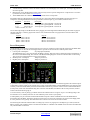
In M2kM, execute Tools -> Memory Editor, click the Radio button for FLASH with the Address at $0000 and click the
Read button. The result should match with the picture below, this is actually the FAT of –M2K ROM
6.
Now click the Radio Button to SRAM, Address $01000 and click Read again. The result should be like above, but with
random rubbish, since SRAM has not been initialized yet. At Address $00000 you should read the copy of – M2K ROM
that you have made earlier (if you have battery backup).
In the data window, click a word and change it. Do a Write and then a Read and verify if the data has actually changed
Use the download button in the ROM/SR Handler to download the current – M2K ROM image at address $00000 from
Flash to your PC. You may save it under any name you like.
7.
8.
9.
The open the tab Erase FLASH and erase Sector 00 (ONLY SECTOR 00!). Use the Memory Editor to verify that bits in
the first ROM image in Flash have been reset to 1’s.
10. Upload the image of –M2K ROM back to Flash and verify again if this has been correctly done. You may also program
SRAM with the -M2K ROM image.
11. For your own peace of mind you may run the memory test Fill and Test in SRAM (will take time!) by starting Tools ->
MLDL Test and then run the random test. Do not run this test in FLASH!
You can now be confident that the MLDL2000 works as it should.
Version 1.50
Meindert Kuipers
6/17/2008
www.kuiprs.nl
Page 12 of 32
MLDL 2000
USER MANUAL
MLDL2000 Software Installation
First download and install FTDI USB drivers before connecting the USB interface to your PC. These can be downloaded form
www.ftdichip.com. Double check if you are using the drivers for the FT2232C controller with D2XX functionality for your
operating system. The combined driver (VCP and D2XX) should work just fine. Install according to the instructions that come
with it.
After the drivers are installed connect the MLDL2000 (plugged in your HP41) to the USB of your computer. A USB hub in
between should not make any difference. Automatic installation is usually fine, just follow the instructions of your PC. Since
the USB controller has two channels it will do the installation twice.
The M2kM software does not require specific installation instructions or registry modifications. Just unpack and install it in a
suitable directory and launch it after the FTDI drivers have been installed. Another file, BORLNDMM.DLL is in the same
zipfile as M2kM, this must be in the same directory as the M2kM executable. M2kM will generate a file MLDL2K.INI with
settings if this file does not already exist. This file must be in the same directory as the executable.
If all is well the Mk2M software should recognize the MLDL2000 with the correct serial number.
Your MLDL2000 is now ready for regular use, have fun! If you have questions, or if the MLDL2000 does not work as
expected, please do the following:
1. Check the MLDL2000 website at www.kuiprs.nl for any updates, latest news, errata and news versions of software,
documentation or firmware
2. Re-read this User Manual and check for any omissions
3. Check all wires and soldering joints. I spent two nights figuring out why something did not work and it turned out to be due
to bad soldering!
4. RTFM: Read the Specifications and this manual and make certain that you fully understand the operation of the
MLDL2000
5. Contact me by email
Version 1.50
Meindert Kuipers
6/17/2008
www.kuiprs.nl
Page 13 of 32
MLDL 2000
USER MANUAL
Using the MLDL2000
This section describes the daily usage of the MLDL2000. Please read these carefully, together with the MLDL2000 Design
Specifications, for a good understanding of the device. It is assumed that you have access to information about the internal
workings of the HP41, especially when working with MCode.
This section is divided in the following topics:
• MLDL2000 Settings Registers
• ROM Images
• Bankswitching
• Power Management
• M2kM Software
MLDL2000 Settings Registers
The MLDL2000 has a lot of memory for ROM module images, much more than the HP41 can handle. Which ROM images the
HP41 sees is managed by the so-called Settings Registers: SR. This is a table which describes an index for every page and
every bank (Page $0 to $F, 4 banks per page) the following attributes:
• ROM Image is enabled or disabled (for example if a regular or system ROM is at that page/bank)
• ROM Image is in SRAM or FLASH memory
• ROM Image is mapped to I/O (only for SRAM images)
• ROM Images in SRAM is Write Protected or Write Enabled
• Rom Image number (8 bits if in FLASH, 6 bits if in SRAM)
During every access that the HP41 attempts the MLDL analyzes the 4 most significant bits of the address that is passed on the
ISA line, these indicate the port being addressed. In combination with information about the current active bank one of 64
Settings Registers from the active set of SR is now addressed and its contents are used to check which part of memory (SRAM
or FLASH) contains the requested ROM image.
Each of the individual 10-bit Settings Registers has the following layout:
Bit 9
EN
EN
Bit 8
FL/SR=1
FL/SR=0
Bit 7
IO
A19
Bit 6
WP
A18
Setting Register Layout
Bit 5
Bit 4
A17
A16
A17
A16
Bit 3
A15
A15
Bit 2
A14
A14
Bit 1
A13
A13
Bit 0
A12
A12
Bit 9:
EN, Enable
0 = FLASH/SRAM/IO Bank is enabled
1 = FLASH/SRAM/IO Bank is disabled
Bit 8: FL/SR: Flash or SRAM
0 = ROM Image is in FLASH
1 = ROM Image is in SRAM
If Bit 9 is 0 (ROM Image is in FLASH) then Bit 5 to 0 have the following meaning:
Bit 7-0: A19-12 for addressing the FLASH memory (or the ROM image number)
If Bit 8 is 1 (ROM Image is in SRAM) then Bit 5 to 0 have the following meaning:
Bit 7: IO, I/O Interface
0 = Bank is SRAM
1 = Bank is IOI
Bit 6: WP: Write Protect (for SRAM only)
0 = Write Enabled
1 = Write Protected
Bit 5-0: A17-12 for addressing the SRAM memory (or the ROM image number)
To access the devices a 20-bit address bus (XA, for eXternal Address) is used with the 16-bit XD (eXternal Data). The top
block of FLASH and SRAM is used to store the Settings Registers. Of the 16 data bits only 10 are actually used.
If an IO Memory bank is indicated, it means that the MLDL2000 will map all access to this bank to the IO interface and the
bank cannot be used for ROM. Bit 0 to 7 are used for data, bit 8 and 9 for status bits, to be used as a basic handshake
mechanism. HP41 Page $4 is the most likely candidate for IO, as this is used exclusively for the Service ROM. An address
window is used to prevent reading of meaningless IO data at critical entry points which would most certainly lead to a crash of
the calculator, see the description of the I/O Interface. Other parts of the IO address window are used for direct access by the
HP41 to FLASH, SRAM and Settings Registers.
NOTE 1:
NOTE 2:
For writing, an SRAM bank does not have to be enabled (bit 0) to allow initializing memory but it must be Write
Enabled.
SRAM banks that do not exist in an HP41 memory map must be write protected, and all Setting Registers must be
initialized at meaningful values to prevent overwriting existing memory contents.
Version 1.50
Meindert Kuipers
6/17/2008
www.kuiprs.nl
Page 14 of 32
MLDL 2000
NOTE 3:
NOTE 4:
NOTE 5:
NOTE 6:
NOTE 7:
USER MANUAL
It is possible to have different SR’s point to the same ROM bank, although this might give unexpected results. This
would be the same as plugging identical modules in multiple ports.
Although multiple IO banks are possible, these all alias to the same physical I/O interface and registers for
accessing SRAM and FLASH.
A disabled bank is best indicated with $3FF in the SR. This allows for non-initialized FLASH to be used as SR that
can be reprogrammed without first erasing the whole block.
FLASH memory is erased by sector, and a sector may contain multiple ROM images and/or Setting Register sets.
FLASH memory bits can only be programmed from ‘1’ to ‘0’. An erase operation (of a complete sector) is required
to set bits from ‘0’ to ‘1’.
With the SR a complete HP41 configuration is described, including potential remapping of the system pages (for example if the
ROMs do not work anymore or are unsoldered). To move a module from one page to another only a change of the SR is
required, the module image in FLASH or SRAM does not have to be moved.
The SRAM memory above $40000 can not be used for storing ROM images, as the SR’s do not allow usage of address lines
A18 and A19. The SR’s are stored in SRAM starting at address $7FF00. The I/O interface allows direct access to this area for
specific applications. Possible future expansions of the MLDL2000 could include access of the SRAM area above $40000 for
emulation of user registers and/or Extended Memory.
The Settings Registers are all in one sector of the FLASH memory. Changing a value may require erasing and reprogramming
of the entire sector! It is therefore best not to keep any ROM images in the sector of the Settings Registers.
For easy switching between configurations, and to recover from lockups, there are 8 (eight) different
sets of SR: 4 in FLASH and 4 in SRAM. The SR in FLASH can be used for more fixed and fully
tested configurations while the SR in SRAM are easily changed. Switching between the configurations
is done with 3 of the DIP switches on the MLDL2000: one switches between SR in FLASH or SRAM
, two switches select which of the SR are being used. The 1st switch is used to completely disable all
communication between the MLDL2000 and the HP41.
Switch 1
Switch 2
Switch 3-4
MLDL_DIS
MLDL_SR
SR_SET[1,0]
OFF:
OFF:
OFF
OFF
ON
ON
-
OFF
ON
OFF
ON
ON
1
2
3
4
MLDL Disabled
ON:
MLDL Enabled
SR from FLASH
ON:
SR from SRAM
SR Set 0, base $FFF00 (FLASH), $7FF00 (SRAM)
SR Set 1, base $FFF40 (FLASH), $7FF00 (SRAM)
SR Set 2, base $FFF80 (FLASH), $7FF00 (SRAM)
SR Set 3, base $FFFC0 (FLASH), $7FF00 (SRAM)
The offset in the table below should be added to the base address as indicated by the settings of the SR_SET switches.
Bank 1
Page 0
Page 1
Page 2
Page 3
Page 4
Page 5
Page 6
Page 7
Page 8
Page 9
Page A
Page B
Page C
Page D
Page E
Page F
$00
$04
$08
$0C
$10
$14
$18
$1C
$20
$24
$28
$2C
$30
$34
$38
$3C
*
*
*
Setting Register Offset
Bank 2
Bank 3
$01
*
$02
*
$05
*
$06
*
$09
*
$0A
*
$0D
$0E
$11
$12
$15
$16
$19
$1A
$1D
$1E
$21
$22
$25
$26
$29
$2A
$2D
$2E
$31
$32
$35
$36
$39
$3A
$3D
$3E
Bank 4
$03
$07
$0B
$0F
$13
$17
$1B
$1F
$23
$27
$2B
$2F
$33
$37
$3B
$3F
*
*
*
* bankswitching not supported in the system pages, see the paragraph on bankswitching
Bank Switching is a mechanism that is used in the HP41 to use multiple ‘banks’ of ROM images in one page, by using
instructions to change the active bank in a page. The mechanism is actually part of the expansion module and the instruction for
switching is decoded and implemented inside the expansion module. The MLDL2000 currently offers only limited support for
bank switching, see the paragraph on bank switching later in this manual.
It is NOT recommended to use any bank of the Pages 0, 1 or 2 in the MLDL2000 since these are reserved for the HP41 system
ROMs.
Version 1.50
Meindert Kuipers
6/17/2008
www.kuiprs.nl
Page 15 of 32
MLDL 2000
USER MANUAL
FLASH Memory Sector Layout
Start
FFF00
F8000
F0000
E8000
E0000
D8000
D0000
C8000
C0000
B8000
B0000
A8000
A0000
98000
90000
88000
80000
78000
70000
68000
60000
58000
50000
48000
40000
38000
30000
28000
20000
18000
10000
08000
04000
03000
02000
00000
End
FFFFF
FEFFF
F7FFF
EFFFF
E7FFF
DFFFF
D7FFF
CFFFF
C7FFF
BFFFF
B7FFF
AFFFF
A7FFF
9FFFF
97FFF
8FFFF
87FFF
7FFFF
77FFF
6FFFF
67FFF
5FFFF
57FFF
4FFFF
47FFF
3FFFF
37FFF
2FFFF
27FFF
1FFFF
17FFF
0FFFF
07FFF
03FFF
02FFF
01FFF
Contents
SECTOR 34, Settings Registers
SECTOR 34, ROM 248-254
SECTOR 33, ROM 240-247
SECTOR 32, ROM 232-239
SECTOR 31, ROM 224-231
SECTOR 30, ROM 216-223
SECTOR 29, ROM 208-215
SECTOR 28, ROM 200-207
SECTOR 27, ROM 192-199
SECTOR 26, ROM 184-191
SECTOR 25, ROM 176-183
SECTOR 24, ROM 168-175
SECTOR 23, ROM 160-167
SECTOR 22, ROM 152-159
SECTOR 21, ROM 144-151
SECTOR 20, ROM 136-143
SECTOR 19, ROM 128-135
SECTOR 18, ROM 120-127
SECTOR 17, ROM 112-119
SECTOR 16, ROM 104-111
SECTOR 15, ROM 96-103
SECTOR 14, ROM 88-95
SECTOR 13, ROM 80-87
SECTOR 12, ROM 72-79
SECTOR 11, ROM 64-71
SECTOR 10, ROM 56-63
SECTOR 09, ROM 48-55
SECTOR 08, ROM 40-47
SECTOR 07, ROM 32-39
SECTOR 06, ROM 24-31
SECTOR 05, ROM 16-23
SECTOR 04, ROM 08-15
SECTOR 03, ROM 04-07
SECTOR 02, ROM 03
SECTOR 01, ROM 02
SECTOR 00, ROM 00-01
The SRAM memory above $40000 can not be used for storing
ROM images, as the SR’s do not allow usage of address lines A18
and A19. The SR’s are stored in SRAM starting at address
$7FF00. The I/O interface allows direct access to this area for
specific applications. Possible future expansions of the
MLDL2000 could include access of the SRAM area above $40000
for emulation of user registers or other purposes.
The FLASH device used is the AM29LV160DB, with a sector size
of 32K words (good for 8 ROM images each). The lowest 4 blocks
are boot blocks and have smaller sector sizes (see table). Since
there is plenty of room in the FLASH memory it is advised to
spread the ROM images as much as possible to allow erasing of
only a single ROM image. After erasing FLASH memory its
contents are set to all 1’s. It is possible to program a bit from 1 to
0, but not from 0 to 1!
Some MLDL2000 units may have a different FLASH memory
layout. This is automatically detected by M2kM, and the exact
layout is shown in the FLASH tab.
The Settings Registers are all in one sector of the FLASH memory.
Changing a value may require erasing and reprogramming of the
entire sector! It is therefore best not to keep any ROM images in
the sector of the Settings Registers.
With the I/O interface as described it is possible to access all of the
SRAM and FLASH from the HP41. Writing to SRAM is also
supported, but writing to FLASH and erasing FLASH is not
supported from the HP41, FLASH can only be programmed
through the USB interface.
ROM Images
ROM Images are soft-copies of existing HP plug-in modules (Application Pacs) like the MATH module, custom modules (PPC
module, HEPAX) or modules that have been privately developed (SANDBOX or M2K ROM). Some modules contain specific
hardware or functions that may or may not be successfully implemented in the MLDL2000. A list of specific modules that is
known to be supported by the MLDL2000 can be found in the appendix. Not supported are modules that have specific I/O, such
as the IL Module, Time Module, Printer, Extended Functions/Memory, Card Reader or Wand (Barcode Reader), although the
ROM images of these modules may be loaded in the MLDL2000 and some functions may work.
The primary means for loading ROM images in the MLDL2000 is by using the USB connection and the M2kM program.
Alternatively a physical module may be copied to the MLDL2000 by using one of the ROM images for Mcode development to
copy a complete ROM Image to MLDL2000 SRAM and then saving it over USB to the PC. It is not possible to copy a ROM
Image directly to FLASH memory from the HP41.
Standard ROMs are 4K * 10 bits, or multiples thereof. Currently M2kM only supports the .ROM format to load and save ROM
Images. In this format a 10-bit ‘word’ is saved in a 16-bit word, with the 6 most significant bits set to zero. M2kM takes care of
the proper conversion. A future version will support the .MOD format as used by Warren Furlow in his V41 emulator.
Please observe copyrights of ROMs and ROM Images!
Bank Switching
Bank Switching is a mechanism that is used in the HP41 to use multiple ‘banks’ of ROM images in one page, by using
instructions to change the active bank in a page. The mechanism is actually part of the expansion module and the instruction for
switching is decoded and implemented inside the expansion module. The MLDL2000 currently offers only limited support for
bank switching, the main limitations are:
• Bankswitching of Page 0, 1 and 2 is not supported (system ROMS)
• Bankswitching for the HP41-CX system ROMS (Extended Functions and Time in page $3 and $5) is not supported
Version 1.50
Meindert Kuipers
6/17/2008
www.kuiprs.nl
Page 16 of 32
MLDL 2000
•
•
•
USER MANUAL
A bankswitching instruction switches the banks in both the even and odd pages of a module port, for example page $8 and
$9 switch together.
HEPAX uses its own bankswitching scheme and can be only used in a special configuration. A separate how-to is written
by Howard Owen and available on www.kuiprs.nl.
The W&W Rambox uses a different bankswitching scheme and is not supoorted.
For ROMS which using bankswitching all unused banks of a page must be filled with the ROM in the last used page. For
example the Advantage ROM has the following .ROM files (ref www.hp41.org, V41 emulator, thanks Warren):
Page,Bank
File Name
Description
n,1
AdvL1-1B.rom
Advantage Pac Lower Page Bank 1 Version 1B
n+1,1
AdvU1-1B.rom
Advantage Pac Upper Page Bank 1 Version 1B
n+1,2
AdvU2-1B.rom
Advantage Pac Upper Page Bank 2 Version 1B
*where n can be 8, A, C or E
Use the following settings in the MLDL2000 when ‘plugging’ the Advantage ROM in MLDL2000 port $8 and $9. If page $9
switches from bank 1 to bank 2, page $8 will switch as well, and therefore bank 2 of page $8 has to be filled with the same
contents as bank 1.
Page $8
Page $9
Bank 1: AdvL1-1B.rom
Bank 1: AdvU1-1B.rom
Bank 2: AdvL1-1B.rom
Bank 2: AdvU2-1B.rom
Bank 3: AdvL1-1B.rom
Bank 3: AdvU2-1B.rom
Bank 4: AdvL1-1B.rom
Bank 4: AdvU2-1B.rom
Power Management
The MLDL2000 was designed to consume minimal power. This may sometimes conflict with the operation of the MLDL2000.
By placing a jumper on J7 on the I/O and Supply PCB it is possible to choose between 3 different power modes:
1. Lowest power consumption
No jumper placed (default)
The MLDL2000 logic is only powered when the HP41 is running. There have been no problems with this configuration, so
this is the recommended setting. The contents of the Bank Switching Registers will be lost when the HP41 is not running.
Tests so far have indicated that this will not cause problems.
2. Medium power consumption
Jumper in position 2-3
3. Highest power consumption
Jumper in position 1-2
2
1
2
3
J3
J1
1
4
6
8
10 12
14
J5
2
4
3
5
1
3
5
7
9
11
13
J7
6
7
J4
8
2
1
3
2
9
10
11
12
3
1
2
1
J6
1
2
J2
It is possible to use an external power source for the HP41/MLDL2000 system. Power should be applied to the external input. It
is important to note the polarity of the external power. In this case the HP41 Battery must be REMOVED, as the external power
is directly connected with the battery terminals inside the HP41 without any protection. Tests so far have indicated that Mode 1
(lowest power) works well with bankswitching. The works fine with the HP41, the HP41CX has an extra protection, and this
results in the BAT indicator going on.
J7 is not suited very well for placing a pin header because the USB B-connector is right on top of it. A soldering bridge is the
best alternative as it is unlikely that users will switch between power modes very frequently.
A backup-battery may be connected inside the MLDL2000 to keep the contents of SRAM valid when the MLDL2000 is
disconnected from the HP41. The battery should provide at least 2.3V and can be connected to J6 on the I/O and Supply PCB.
It is also possible to use a goldcap. The schematic for this is shown in an earlier section of this manual.
Disconnecting the USB cable while the HP41 is running may result in very high power consumption (up to 30mA) while the
HP41 is running. This condition returns to normal when the HP41 is in SLEEP or STANDBY mode. Disconnect the USB cable
only when the HP41 is turned off.
Version 1.50
Meindert Kuipers
6/17/2008
www.kuiprs.nl
Page 17 of 32
MLDL 2000
USER MANUAL
M2kM Software
NOTE: M2kM is constantly being changed. Please check regularly on www.kuiprs.nl/hp41 for updates. Some menu items
mentioned may be disabled and the screenshots in this manual may differ from the most recent version. The description in this
version of the manual is valid for version 1.50. Of course I assume no responsibility for damage, crashes, blue screens and other
disasters.
There is only one version of M2kM. For testing and production I have exactly the same version. This allows me to support you
in case of problems by taking over your computer over the internet and use some of the special functions that you should not
normally use, or to instruct you to use these. The functions are potentially dangerous, although I have no proof that they can
cause any physical harm to the MLDL2000 or HP41. So you have these functions available, but please keep away from them,
unless specifically instructed. The functions are described in this manual to a certain extent and the descriptions contains
warnings.
M2kM is written in Borland Delphi and requires a specific dll: BORLNDMM.DLL. This is available from my website.
NOTE: The current version of M2kM does not support auto detection of plugging and unplugging the MLDL2000. It is
therefore advised to connect the MLDL2000 before starting M2kM and not to disconnect it while M2kM is running.
Attempting to communicate with an unconnected MLDL2000 may result in crashing the M2kM application or in extreme cases
may require a reset of the host PC.
Before using M2kM please install and test the FTDI USB driversM2kM (MLDL2000 Manager) software is used to
communicate between the MLDL2000 and a PC using a USB connection. Only the Windows XP operating system (SP2) is
tested. The basic functions of M2kM are:
• Uploading ROM images to FLASH and/or SRAM
• Downloading ROM images from FLASH and/or SRAM
• Erasing blocks of FLASH memory
• Managing the Settings Registers
• Communication between the HP41 and the PC
• Testing of the MLDL2000
• Modifying the MLDL2000 operation by loading a new firmware version
• Disassembly of ROM images
Standard ROMs are 4K * 10 bits, or multiples thereof. M2kM supports the .ROM and .MOD format to load and save ROM
Images. M2kM takes care of the proper conversion. The ROM and MOD formats are supported by various other HP41
programs, like Warren Furlows V41 PC simulator (see www.hp41.org ).
After launching the M2kM application you will see the main ROM Handler window with menu and status bar. The status bar
will show if the MLDL2000 is connected and initialized and also shows the serial number, firmware version and memory type
of your MLDL2000.
Through the menu the following choices are possible:
File
- Open
- Save
- Exit
Opens a ROM, MOD or SR file
Saves a ROM or SR file
Leave the M2kM application
Connection
- Connect
- Disconnect
Connect and initialize MLDL2000 connection after plugging in
Disconnect MLDL2000 before unplugging
Tools
- Memory Editor
- CPLD Upgrade
- MLDL Test
- BitBang
Random access to MLDL2000 Memory
Upgrade contents of CPLD
Test of MLDL2000 (handle with care!)
Individual control of the MLDL2000 I/O signals (handle with care!)
Preferences
- Preferences
change the default settings of M2kM
Help
- About
shows the version of the M2kM application
Connecting and Disconnecting the MLDL2000
When launching the application it will automatically check if an MLDL2000 is connected and will show the serial number,
firmware version and memory configuration if it finds one. If not, all functions that communicate with the MLDL2000 will be
disabled. You may connect the MLDL2000 later and use Connection - Connect for initialization. If you want to keep M2kM
running and want to unplug the MLDL2000 first use Connection - Disconnect before pulling the plug. Automatic detection of
plugging/uplugging of the MLDL2000 is not supported.
Version 1.50
Meindert Kuipers
6/17/2008
www.kuiprs.nl
Page 18 of 32
MLDL 2000
USER MANUAL
Communication Speed
When transfer of data between the PC and the MLDL2000 is unreliable, please decrease the Communication Speed with the
Preferences dialog. The default speed is high enough to be comfortable, but is some cases there could be problems. The
presence of other USB devices or hubs on the system may influence the communication speed. Firmware upgrading should
normally be done at lower speed, therefore the JTAG speed is usually lower than the normal communication speed. You may
also try to increase the communication speed. Maximum speed is 6 mbit/s. See the section on Preferences for more information.
Handling MLDL2000 ROM Images and Settings Registers
The ROM/SR Handler will be the most used tool for communicating with the MLDL2000. It contains 4 tabs for the following
functions:
• ROM: up-downloading ROM images, saving and retrieving ROM images, the disassembler and creating backups
• Settings Registers: handling the SR’s and the MLDL2000 contents
• FLASH Erase: erase blocks of FLASH Memory
• MOD file editor: open, edit and save MOD files
ROM Handler
The Status Bar will always indicate the current open file, selected memory type and status. It also contains a progress bar to
monitor up- and downloads.
The ROM Handler tab is the central part of M2kM. It represents the current open .ROM file or the ROM image that has been
downloaded. The MOD Handler tab uses the current ROM as a reference as well. Only the current ROM can be disassembled,
meaning that in many cases the ROM image in a MOD file must first be copied to the current ROM. The current open ROM
file is different from the open MOD file!
•
•
•
•
•
Open button: will open a .ROM, .MOD or .SR file, and lists some characteristics in the window. The tab will
automatically change to the relevant part.
Save ROM button: saves the current open .ROM file (may be a ROM image downloaded form the MLDL2000).
Upload button: will copy the open ROM image to the MLDL2000. When a MOD file is open, only the first image will
be uploaded to the ROM number indicated
Download button: copies a ROM image from the MLDL2000 and lists some characteristics in the window.
Verify button: checks the contents of MLDL2000 against the current open ROM image.
Version 1.50
Meindert Kuipers
6/17/2008
www.kuiprs.nl
Page 19 of 32
MLDL 2000
•
•
•
USER MANUAL
ROM Number edit/up-down control: indicates the ROM number for up- or download. The actual ROM address will
be shown below it. ROM Number and Address will be recalculated according to choice of FLASH/SRAM.
SRAM/FLASH radio button: indicates memory type for up-or download.
Auto checkbox: enables automatic searching for the first free ROM page.
NOTE: When uploading to FLASH Memory the target page will be checked. If it is not erased (all words $FFFF),
programming is not possible since FLASH memory bits can only be programmed from ‘1’ to ‘0’. In that case the complete
sector containing the ROM needs to be erased first. First save any other ROM images in that sector. This check is not done
when uploading to SR’s. A time-out will occur when attempting to program a bit from 0 to 1.
Programming FLASH takes more power than normal operation. The HP41 should be connected and powered.
Uploading ROM images
The Upload function copies a ROM image to the MLDL2000. It uses the settings in the toolbar for ROM Number and memory
type. There is no check for overwriting existing content to SRAM. Overwriting FLASH is generally not possible, unless the
page is erased first. The Auto Checkbox may be used to automatically find the first free ROM page in the selected memory
type. Since it will communicate with the MLDL2000 more frequent it may disrupt any ongoing operations in the HP41. This
also happens when M2kM is started. The algorithm behind it checks the first 16 words of a ROM page. When it finds any bit
set to 1 in the 6 most significant bits of any of the words (these bits are not used by the 10-bit ROM words) it will decide that
the page is not is use. For SRAM this means that there was random data, for FLASH is means that it was erased. If not all of
FLASH was erased this will be discovered when writing to the page.
Downloading ROM images
The Download function copies a ROM image from the MLDL2000 to the Rom Handler. It uses the settings in the toolbar for
ROM Number and memory type. The Auto checkbox must be unchecked, and the relevant ROM must be selected. An easier
way to select and download ROM images is by using the SR Handler, where a ROM can be picked from the Contents list.
Disassembler
The Disassembler will allow disassembly of the current open ROM image. The disassembly listing will be shown in a separate
window as text, from where it can be selected and copied to another application, for example to be saved or edited.
The checkbox ‘ROM has FAT’ is checked by default, but should be unchecked when disassembling ROM images which do not
have a FAT, for example the HP41 system ROMs. The Disassembler Base Page should be used when a ROM image has a
known page in the HP41 address map.
•
•
•
•
•
•
•
List FAT button: lists the FAT of the current ROM. When a 2nd ROM is loaded and Disasm 8K is selected it will list
both FAT’s. Do not use base pages 0 to 2 when there are labels in the FAT area as some XROM numbers might not
show correctly.
ROM Header button: lists the header of the current ROM file or of both if Disasm 8K is sleceted
Disassemble button: starts the disassembler
Move to 2nd 4K button: copies the current Rom to the 2nd 4K page for disassembly
ROM has FAT checkbox: use this to indicate if a FAT has to be disassembled (uncheck when disassembling the
system ROMs for example)
Disasm 8K ROM checkbox: enables disassembling of an 8K ROM
Disassembler Base pulldown: choose the base page for the disassembler.
The Disassembler uses 2 external files: XROM.txt and SYSTEMLABELS.TXT. These are text files that supply standard
XROM numbers and the names and addresses of the system entry points (Mainframe Labels). An explanation of the format is
in the files. These files may be edited with other XROM numbers or labels as required.
To disassemble an 8K ROM, use the following steps:
1. Open the 2nd 4K ROM image
2. Click [Move to 2nd 4K]
3. Open the first 4K ROM image
4. Check the box DisAsm 8K ROM
5. Click DisAsm
When disassembling 8K ROMS, the Base Page will always be an even page (the 2nd block will be in the odd page).
Currently, the Disassembler has the following features:
• System entry points are read from SYSTEMLABELS.TXT (this may be switched off in Preferences)
• When a ROM with a base Page from $0 to $7 is disassembled, the local labels are read from SYSTEMLABELS.TXT
(this may be switched off in Preferences). Use this when disassembling the system ROMs,
• XROM numbers are read from XROM.TXT (this may be switched off in Preferences)
Version 1.50
Meindert Kuipers
6/17/2008
www.kuiprs.nl
Page 20 of 32
MLDL 2000
•
•
•
•
•
•
USER MANUAL
Automatic comments are generated for local GOSUB, and XROM’s, comments for system labels or XROM’s are read
from SYSTEMLABELS.TXT or XROM.txt (this may be switched off in Preferences). Local XROM numbers are
generated from the disassembled ROMs own FAT.
User code is recognized and disassembled
Labels for jump address are automatically generated (this may be switched off in Preferences)
ROM checksum is verified
Mnemonics type may be chosen in the Preferences Dialog (Jacobs/De Arras, HP or Zencode)
Multiple consecutive (more than 3) NOPs may be skipped (see Preferences). Only NOPs that do not have a label will
be skipped. In some cases labels may be generated by disassembling data.
There are also some limitations:
• Disassembly is never perfect. It is not always possible to distinguish data from instructions, in many cases data is
incorrectly disassembled as instructions. This may also generate labels that are never jumped to.
• Function names and User Code which have their FAT in another Page (which is the case for many 8K ROMS) may
have their function names and User Code incorrectly disassembled as mcode. Resolve this by disassembling both
ROMs at the same time as an 8K ROM.
• Some ROMs have adjacent function names without instructions in between. These are shown in the FAT, but not
correctly in the disassembly listing.
• Synthetic characters in User Code and special HP41 characters in function names (Sigma etc) are not displayed
correctly, therefore the hex codes are listed behind these strings.
• When disassembling .MOD files, the ROM images must be moved to the ROM Handler first.
• When disassembling random data, the disassembler may be stuck in an endless loop.
Various options for the Disassembler can be set in the Preferences dialog.
Backup and Restore
Backups are created in MOD files. The created MOD file has a special attribute to indicate that it is an MLDL2000 backup.
MLDL2000 serial number, firmware version and date/time are written in the comments. Every module image has the Custom
Header set to indicate memory type and address. A special attribute has been created for SR backups. It is possible to have
more than 255 pages images in one MOD file, but this is not compatible with V41!
SRAM, FLASH and SR’s can be individually saved and restored, this is indicated the checkboxes. When backing up FLASH or
SRAM, the user can choose to save all ROM pages, including those which are not used (are not shown in the list in the SR
Handler). This may be useful when there is custom information stored in FLASH or SRAM. Note that these pages are not
automatically restored. MOD files only save a 10-bit word, while FLASH and SRAM have 16-bit words. For normal HP41
code and SR’s this is not an issue, because
A backup MOD file may be manipulated like any MOD file, ROM images can be individually extracted, uploaded, etc. When
there are more than 255 images in one MOD file it is not possible to add pages but deleting pages is possible.
The restore functions will restore the contents of a backup MOD file to the MLDL2000. Note that any previous contents will be
overwritten, and that all FLASH will be erased first. Use the MOD file Handler for restoring individual ROM images. The SR
checkbox indicates if the SR’s are restored as well. Pages which were marked as empty or unused will not be automatically
restored.
Restoring SR’s is a bit more complicated, since the complete sector must be erased first if these were in FLASH, and this might
erase ROM images. Therefore SR’s should be saved to SRAM first. Using the SR Handler the SR’s can be individually
downloaded from SRAM, edited, and uploaded to FLASH. Of course, if the SR’s in SRAM were in use, these should be backed
up first.
Changes to the MOD file format:
• Additional Category:
MLDL2000_backup = 8
• Additional Page:
SR Backup = $8F
• NumPages is $FF when there are more than 255 images in the MOD file
• HeaderCustom definition: Byte 0 $A5, identifier for MLDL2000 backup
Byte 1 Number of images DIV $100
Byte 2 Number of images MOD $100
• PageCustom definition: Byte 0 $A5, identifier for MLDL2000 backup
Byte 1 $01 - SRAM (bit 0, lsb)
$02 - FLASH (bit 1), bit 0 or 1 is always set
$04 - ROM (bit 2)
$08 – SR (bit 3), bit 2 or 3 is always set
Byte 2 MLDL2000 ROM number, $00 for SR, $FF for empty page (FLASH only)
Version 1.50
Meindert Kuipers
6/17/2008
www.kuiprs.nl
Page 21 of 32
MLDL 2000
USER MANUAL
Settings Register Handler
The Settings Register Handler allows easy editing of the Settings Registers. The Listing window allows expansion of the Page
in the 4 possible banks. Please refer to the paragraph about the Settings Registers for more details. The file format allows for
comments. For a better overview the splitter between the SR tree and MLDL2000 contents list can be moved.
The file format for the .SR files is based on a text file for easy off-line editing. See the example SR file that comes with M2kM.
The Status Bar will always indicate the current open file, selected memory type and status. It also contains a progress bar to
monitor up- and downloads.
•
•
•
•
•
•
•
•
•
•
•
Open button: will open a .sr file, and will list the contents.
Save button: will save the open .sr file.
Upload button: will copy the open SR’s to the MLDL2000.
Download button: copies SR’s from the MLDL2000.
Verify button: checks the contents of MLDL2000 against the current open ROM image.
SR Number edit/up-down control: indicates the SR number for up- or download. The actual SR address will be shown
below it. SR Number and Address will be recalculated according to choice of FLASH/SRAM.
SRAM/FLASH radio button: indicates memory type for up-or download
Default SR button: Reset the current SR to $3FF, which indicates a disabled ROM.
Default ALL button: Reset all SR’s to $3FF.
Collapse/Expand All button: Collapses or Expands the treeview.
List MLDL button: lists the contents of the connected MLDL2000.
The ROM Number and SR attributes (the 4 checkboxes) allow easy editing of the SR contents. The SR that is selected in the
treeview will be updated after every change.
Right clicking in the SR tree will give various options for collapsing or expanding part of the tree.
When the MLDL List is present and an SR configuration is available, the ROM names will be shown in the HP41 Page
Overview (if they are part of the current configuration). Selecting a ROM Page and Bank on the left hand side, and double
clicking a ROM in the right window, will add that ROM to the SR overview to build a complete configuration. The individual
SR settings may then be modified. When finished the SR configuration may be saved. Do not forget to upload the configuration
to the MLDL2000, in the correct SR, to activate it and set the dipswitches to the matching position. Clicking the titles on the list
header will sort the list.
Version 1.50
Meindert Kuipers
6/17/2008
www.kuiprs.nl
Page 22 of 32
MLDL 2000
USER MANUAL
The List MLDL function only finds ROM images that have the 6 most significant bits set to 0 in the first 16 words of the
image, otherwise it will assume that there is no valid image. This means that images with all zeroes will be found. It is very
unlikely that uninitialized SRAM (with random contents) will be detected as a valid ROM.
Right-clicking on a ROM image gives the following options:
• Refresh List: Re-reads the list from the MLDL2000, same as the List MLDL button
• Download: download the selected ROM image to the current ROM
• Save As: download and save the current ROM.
• Wipe SRAM: only works on SRAM: will fill the first 16 words of the selected ROM images with $FFFF and
effectively removes the ROM image from SRAM. It will not show again in the list. Select Refresh List to verify this.
Multiple ROM images may be selected by holding the SHIFT or CONTROL key while selecting the ROMS, FLASH
pages will not be erased.
• Append to MOD: append the selected ROM images to the current open MOD file. Will not work if there is no MOD
file open (see MOD File Handler)
NOTE: When uploading an SR configuration FLASH Memory, there is no check if the data can actually be programmed.
FLASH memory bits can only be programmed from ‘1’ to ‘0’. A time-out error will occur when attempting to program a bit
from ‘0’ to ‘1’. In that case the complete sector containing the SR must be erased first.
When experimenting with the Settings Registers, always do this in SRAM, since the individual bits may be changed if a
mistake is made. This is much more difficult in FLASH, because the complete sector containing the SR’s must normally be
erased, wiping out all other SR’s in the process. There is no functional difference between SR’s coming from FLASH or
SRAM. Once a certain SR configuration is final, just download it from SRAM, select FLASH in the FLASH/SRAM radio
button and choose 1 of 4 SR sets, and then program to FLASH.
FLASH Erase Handler
The buttons for Open, Save, are not relevant here.
The list window allows selection of one of the FLASH Memory sectors. It is not possible to select multiple sectors. Depending
on the FLASH type used in your specific MLDL2000 version, the sector layout may differ.
•
•
ERASE SECTOR button: Erases the selected sector.
ERASE ALL button: Erases the complete FLASH memory. This may take up to one minute and no progress bar is
shown.
Version 1.50
Meindert Kuipers
6/17/2008
www.kuiprs.nl
Page 23 of 32
MLDL 2000
•
•
•
•
USER MANUAL
Chk Sector Empty button: verifies if the selected sector is indeed empty. When it is not empty, the address of the first
non-$FFFF word will be shown in the statusbar. The check stops at the first non-$FFFF word is finds.
Chk ALL Empty button: verifies all of FLASH memory (may take a longer time depending on the communication
speed and block size settings) and shows empty sectors. If a sector is not empty, the address of the first non-$FFFF
word will be shown in the statusbar. The check stops within a sector after the first non-$FFFF word it finds.
Read FLASH Type button: re-reads the FLASH memory type. This is done automatically after connecting the
MLDL2000.
Reset FLASH button: Under certain circumstances the FLASH memory may ‘hang’ in a programming mode, for
example after a time-out. This can be verified by reading an alternating pattern from FLASH. Use this button to
recover from that situation.
The time-out values may be changed in the Preferences dialog. This is not recommended, but may be required in rare
circumstances, for example when the FLASH cells have been programmed many times and become more difficult to reprogram
or erase. The FLASH cells are normally guaranteed at least 1 million write cycles per sector.
Erasing and programming FLASH takes more power than normal operation. The HP41 should be connected, preferably
powered by an external adapter.
MOD File Handler
MOD Files are container files that may hold up to 256 ROM images. The advantage is that, apart form the ROM image itself, a
MOD file also contains information about the type of ROM, comments, manufacturer and how it should be used. MOD files are
introduced by Warren Furlow for his V41 emulator. The exact format is described in the V41 sources that can be downloaded
from www.hp41.org. The MLDL2000 uses some minor additions to some of the field definitions.
MOD files may be created, opened, edited, saved and up- and downloaded from the MOD File Handler in M2kM. Automatic
configuration like in V41 is not supported by M2kM. For disassembly the ROM image must be copied to the ROM Handler.
The MLDL2000 backups are in MOD file format.
When opening a MOD file, the ROM images are shown in the list on the left. The MOD file header is shown on the top right,
the Module Characteristics of the first ROM on the lower right. Clicking one of the ROMs will show its contents on the lower
right. Note that the ROM image itself cannot be edited, only the parameters in the headers. Some information from the image is
shown. A backup copy of the MOD file is made immediately after opening the file. It has the same name as the MOD file with
the extension .BAK. Clicking the headers in the list will sort the list. When opening a MOD file, some checks are done to
prevent opening a file with non-compatible contents.
Version 1.50
Meindert Kuipers
6/17/2008
www.kuiprs.nl
Page 24 of 32
MLDL 2000
USER MANUAL
Manipulation of the MOD files can be disk intensive. Only one ROM image is kept in memory, the other images are read
whenever these are requested. Edits must be specifically saved before selecting a different ROM page in the MOD file. The
various fields may be edited at any time. In some cases changes are immediately written to disk.
Backup files form the MLDL2000 are stored as MOD file, and can be handled as such without problems. Care should be taken
when the backup file contains the Settings Registers. These can be recognized by the Custom Header, and the value of the Page
(this will be $8F). It is possible to handle the SR backup just as a normal ROM image, but the results will be unpredictable.
To Save, Apply or Cancel edits made in the MOD file:
• Save Edits button: Will write the changes to disk for both the MOD file header and the ROM.
• Apply Edit button: Activates the changes, the various fields will be updated and refreshed. Edits are not yet written to
disk.
• Cancel Edit button: Restores the original contents of the MOD file fields. Must be done before clicking Save or Apply.
Manipulation of the MOD file (some functions are available only in the popup menu in the list).
• Reread File button: Re-reads the file from disk and updates the list with the changes that may have been done.
• New MODf button: Creates a new MOD file with zero ROM images and an empty header, the Save As dialog will be
started.
• Close MODf button: Saves and closes the current MOD file.
• Save>ROM button: Saves all selected pages to .ROM files. The name of the ROM (Module name in Header) will be
used as the filename, it there is no name or the file exists, the Save As dialog will be shown.
• ROM>MOD button: Appends the current open ROM from the Rom Handler (this may be downloaded from the
MLDL2000 or opened from disk) to the current MOD file. The ROM page parameters are cleared and may be edited.
If the checkbox Image has FAT was selected before clicking ROM>MOD the name field will be filled. The ID+Rev
field will always be filled from the image contents. Click Save Edits and ReRead File. Multiple ROM images may be
added to the MOD file in this way. A maximum of 255 ROM images can be in any single MOD file. When the
Overwrite checkbox is checked the first selected ROM image will be overwritten.
• Overwrite checkbox: when checked the ROM>MOD function will not append, but overwrite the current selected ROM
image. To prevent unintended overwrites the checkbox is cleared after every ROM>MOD action.
• INS MOD: this button inserts an empty page before the selected page. This is done in the order the pages are in the
MOD file, the actual sort order in the list is ignored.
• DEL MOD: removes all selected pages from the MOD file. Confirmation is asked.
Upload ROM: Uploads the selected ROM images to the MLDL2000. See explanation below.
When uploading ROM images to the MLDL2000 the MOD Upload options (radio buttons) are active in combination with the
ROM # (and address) and Auto checkbox. When a MOD file contains Settings Registers (for example from a backup) these will
not be uploaded. Multiple selected pages may be uploaded and the free pages will be automatically found with the algorithm
used to find ROMs in the SR Handler, modules occurring in that list will not be overwritten. FLASH will always be check if it
is erased. The following options can be used:
• When the Auto checkbox (in the button bar) is not checked, only manual loading is supported, the MOD Upload
Options are ignored. The ROM number and Memory Type as indicated in the button bar will be used, and only the
first selected image will be uploaded. Uploading will be just like loading a single image from the ROM Handler.
• When the Auto checkbox is checked, multiple selected images may be uploaded. This is always done in the order as
the images appear in the list. When errors occur, the complete upload will be aborted. The radio buttons in MOD
Upload Options are used as follows:
o Auto from Button Bar: will automatically find free ROM space in the memory type indicated by the
SRAM/FLASH radio button. All selected pages will be uploaded if there is enough free space. FLASH
memory will be checked first if it is erased.
o Auto from MOD contents: same as option above, with the exception that pages which have the RAM attribute
set (in the MOD file header) will always be uploaded to SRAM, other pages will be uploaded to FLASH or
SRAM as indicated in the button bar.
o Auto from MOD backup: the settings in the button bar will be ignored, the custom header field will be used to
individually restore pages from a backup file. Note that in this case an existing ROM in SRAM may be
overwritten.
In the list multiple ROM images may be selected by holding the SHIFT or CONTROL keys while selecting a ROM. Right
clicking in the list activates a popup menu with the following choices (some of the functions above are also available in the
popup menu):
• Delete Selected Pages: Deletes the selected ROM images from the MOD file. Confirmation is asked.
• Insert Before Selected: inserts an empty page before the selected page. This is done in the order the pages are in the
MOD file, the actual sort order in the list is ignored.
• ROM>MOD: (append or overwrite): appends (or overwrites) the current open ROM from the Rom Handler, see
ROM>MOD button.
Version 1.50
Meindert Kuipers
6/17/2008
www.kuiprs.nl
Page 25 of 32
MLDL 2000
•
•
•
•
•
•
USER MANUAL
Reread File: Re-reads the file from disk and updates the list with the changes that may have been done.
Extract to ROM Handler (1st 4K or 2nd 4K): Copies the ROM contents to the ROM Handler for saving as .ROM,
disassembly, up- or downloading. When multiple pages are selected, the second one is copied to the 2nd 4K block..
Extract to SR Handler (0..3): Copies one of the SR’s from the MOD file to the SR Handler for verification or
uploading to the MLDL2000. It is not possible to immediately upload an SR to the MLDL2000. The contents must
come from an SR backup, and the SR page must be selected, otherwise the result in the SR handler will be undefined.
Extract selected to .ROM file: Saves all selected pages to .ROM files. The name of the ROM (Module name in
Header) will be used as the filename, it there is no name or the file exists, the Save As dialog will be shown.
Extract to SR file: Extracts all 4 SR backups to an .sr file. The name is taken from the Page Name field. If this name is
undefined, a new filename will be prompted for. 4 files will be created, with the name ending in ‘_srx’, x is 0..3. The
individual files may be opened with the SR Handler for editing and/or uploading.
Upload to MLDL2000: See Upload button.
To add a ROM image which is in the MLDL2000, it must first be downloaded to the ROM Handler, or it can be appended to
the current MOD file from the list in the SR tab. The last option supports adding multiple (or all) ROM images. When adding
multiple ROM images, the file is immediately written to disk and it is assumed that the ROMs have a FAT to update the ROM
name and ID/Rev. Also the Custom Header of the ROM page will be filled with the MLDL2000 address and memory type in
the same way as in the MLDL2000 backup files.
NOTES
Uploading (multiple) ROM images from MOD files to the MLDL2000 still require the user to create the correct SR settings.
For example the Write Protect attribute from the MOD file must be set in the correct way in the SR’s, otherwise there will be no
write protection. MOD files created with M2kM may not always work in the V41 emulator, depending on the settings of the
attributes. After the upload, refresh the module list in the SR handler to check where the images have ended up.
M2kM used the Custom Header sections. This may conflict with other applications using these fields.
M2kM defines extra attributes for storing SR’s and backups. MOD files created with these attributes should not be loaded in
V41.
Future changes in V41 may results in different MOD file definitions and interoperability cannot be always guaranteed.
The MOD file will remain open for reading and writing in M2kM until specifically closed, until another MOD file is opened or
until M2kM is closed. When the file is open, other applications like V41 may have no access to the file.
Preferences
The Preferences dialog is used to set the default
settings of M2kM.
There are two sections, one for the Disassembler,
and one for Communication. Apart from the
settings in the preferences screen, some other
options are automatically saved in the m2km.ini
file:
• Screen positions and sizes of all windows
• Position of splitter in SR tab
• Memory type (SRAM or FLASH)
The effects of the Preferences settings are as
follows
• Auto Comments: enable the automatic
generation of comments that are read for the XROM.TXT or SYSTEMLABELS.TXT file. When unchecked, no
comments are generated at all
• Auto Label Generation: the disassembler generates labels when it finds a jump or execute to an address, for the
function entries, FAT and at many other points. A label is shown in the disassembly listing for these locations in the
form of LBL_1234, where 1234 is the address. When unchecked, no labels are generated at all
• Use MainFrame Label File: enable use of the SYSTEMLABELS.TXT file for translation of address into text for
jumps/executes, and also for generating labels when diassembling system pages.
• Use XROM file: enable use of the file XROM.TXT when disassembling user code for translating XROM numbers in
function names with possible comments.
• Skip Multiple NOPS: causes the disassembler to skip NOPS if there are more than 3.
• Mnemonics Type: sets the preferred mnemonics type.
Version 1.50
Meindert Kuipers
6/17/2008
www.kuiprs.nl
Page 26 of 32
MLDL 2000
•
•
•
•
•
•
•
USER MANUAL
Comm Speed: Defines the default communication speed between the USB controller and the MLDL2000. A value of 0
indicates the highest speed (6 mbit/s), a value of 65535 the lowest speed. Increase the value when communication is
unreliable. Normally the speed should be as high as possible, and 6 mbit/s should work in most cases. The
communication speed may depend on the USB cabling, use of USB hubs, performance of your computer and or
diskdrive and possible other factors.
Comm Block Size: Defines the default USB communication block size. The larger the block, the faster the
communication. Change the value when communication is unreliable.
JTAG Speed: Defines the communication speed between the USB controller and the MLDL2000 when upgrading
firmware. This should be about 300 kbit/s. A value of 0 indicates the highest speed (6 mbit/s), a value of 65535 the
lowest speed. Increase the value when Firmware upgrading is unreliable.
USB Timeout: Defines the default USB timeout value (in milliseconds) when M2kM is communicating with the
MLDL2000. Failures may occur, for example when unplugging the USB cable. This value should not normally be
changed.
Flash Prog Timeout: Defines the FLASH timeout value (in milliseconds) when writing a single word to FLASH. This
timeout occurs when attempting to program a ‘1’ to a ‘0’, or when the FLASH is damaged.
Sector Erase Timeout: Defines the FLASH timeout value (in milliseconds) when erasing a sector. Errors may occur
when there is not enough power (low BAT). Sectors are normally erased in about 300 milliseconds.
Erase All Timeout: Defines the FLASH timeout value (in milliseconds) when erasing the complete FLASH memory.
Normally erasing takes about 30 seconds. Errors may occur when there is not enough power (low BAT).
The time-out values for programming or erasing should normally not be changed, but may be required in rare circumstances,
for example when the FLASH cells have been programmed many times and become more difficult to reprogram or erase. The
FLASH cells are normally guaranteed at least 1 million write cycles per sector. When errors occur, first reset FLASH and
verify if the HP41 has enough battery power.
• Auto Verify: Enables automatic verify after downloading a ROM or SR’s. Verify is always done after uploading.
• Confirm Download: Requires confirmation before downloading a ROM or SR. Confirmation is always required when
uploading a ROM.
• Auto Find Free ROM: Enables automatic search for free ROM space in the MLDL2000. This will enable more
frequent and automatic communication with the MLDL2000, which could disrupt operation of the HP41.
• SRAM default Memory Type: Will set SRAM to the default memory type for up- and downloads.
CPLD Upgrade (JTAG Mode)
The CPLD contains the MLDL2000 Firmware. The firmware may be upgraded when new functionality becomes available or
when bugs are resolved.
Firmware Programming is a critical operation, please do only when required. Do not use any of the debugging features, when in
doubt please ask. The debugging functions are there to be able to support you in case of problems. Firmware upgrading takes
more power than normal operation. When programming new firmware, have you HP41 connected and powered. Do no use your
HP41 during firmware programming and use fresh batteries or an external power adapter. Do not disconnect the USB cable and
only use trusted firmware files.
Version 1.50
Meindert Kuipers
6/17/2008
www.kuiprs.nl
Page 27 of 32
MLDL 2000
USER MANUAL
Instructions for use:
• Check the Device ID, this must be $0495B093
• Check the current Firmware Version (Device ID is shown as well)
• If no errors occur, firmware may be upgraded
• Click OPEN to choose the firmware file, must have the .XSVF extension
• Click PROGRAM to do the actual programming. The progress bar is shown. The actual programming consists of 4
steps, although these steps are not individually shown:
1. Erasing current firmware
2. Programming new firmware
3. Verify new firmware. Any programming problems will be visible during this step
4. Program Firmware version string (only after successful programming)
• During Firmware programming, the contents of the first block of SRAM may become corrupted. It is strongly advised
to make a backup of the entire MLDL2000 SRAM and restore it after programming.
• Should Firmware programming fail, decrease the JTAG Speed (in the Preferences dialog) and try again. The default
JTAG Speed is already lower than the regular communication speed.
• After successful programming, verify the operation of the MLDL2000 by doing a CAT 2 of some ROMs that are in
the MLDL2000, and download a ROM image. A full test is not required.
BitBang
Please do not use this function. It is available for production and test/debug purposes only.
Memory Editor
The Memory Editor is useful for direct inspection and modification of SRAM and /or FLASH contents without the limitations
of the ROM and SR Handler. It should be used with care.
• FLASH/SRAM radio button: Selects between SRAM and FLASH memory
• Address edit: start address of the listing.
• Read button: reads 256 16-bit words starting at Address.
• Write button: Writes all 16-bits words to the selected address.
• Up Arrow button: increases the Address by $10 and read.
• Down Arrow button: decreases the Address by $10 and read.
• Up 256 button: increases the Address by $100 and read.
• Down 256 button: decreases the Address by $100 and read.
• Up 4K button: increases the Address by $1000 and read.
• Down 4K button: decreases the Address by $1000 and read.
Data may be changed by selecting a cell and editing the information. There is no specific error checking of the edited data. The
Write button writes all data in the edit windows back, it does not check if data is actually changed. After the write operation the
block is read again.
NOTE: When changing words in FLASH Memory, there is no check if the data can actually be programmed. FLASH memory
bits can only be programmed from ‘1’ to ‘0’. A time-out error will occur when attempting to program a bit from ‘0’ to ‘1’.
NOTE: SRAM addresses above $7FFFF do not exist, but are aliased with the lower part of SRAM except on the units with 2*
SRAM.
Version 1.50
Meindert Kuipers
6/17/2008
www.kuiprs.nl
Page 28 of 32
MLDL 2000
USER MANUAL
MLDL TEST
The TEST window is used for ‘production’ test of the MLDL2000. Not all tests are currently implemented. Only the memory
tests can be used. The button Shipping Config relies on absolute file paths and should not be used. The memory tests will fill
the FLASH and/or SRAM with a random pattern, starting with a fixed seed. The random pattern is regenerated again while
reading the memory contents. The random pattern virtually guarantees that any shorts or bad connections between traces on the
PCB are detected. It may miss defects in individual memory cells.
Testing memory may take a long time, so please be patient. The tests can be interrupted with the STOP button (erasing FLASH
cannot be interrupted).
•
•
•
•
•
•
•
•
•
•
•
TEST SRAM button: Will test SRAM, or the 2* SRAM configuration is that checkbox is checked
TEST FLASH button: Will test FLASH. FLASH memory will be erased!
QUICK SRAM button: Will do a test of the first 4K SRAM block only
QUICK FLASH button: Will do a test of the first 4K FLASH sector only. The sector containing the block will be
erased first.
TEST ALL button: First do a full SRAM test, then a full FLASH test
QUICK ALL button: First do a QUICK SRAM test, then a QUICK FLASH test (see above)
2* SRAM checkbox: for double SRAM configurations
Detailed Results checkbox: when checked, all errors with the offending address and data will be shown, otherwise
only one error message per block will be shown.
MEMORY TEST radio buttons: selects the type of test. Fill Only will one write the memory, not test, Test Only will
only test the memory, and not fill it before. Fill and Test will do both.
Shipping Config button: Prepares the MLDL2000 in the default configuration. This depends on absolute file paths and
should not be used.
SRAM only checkbox: Prepares the MLDL2000 in the default configuration for SRAM only, FLASH is not
programmed. This depends on absolute file paths and should not be used.
The test progress and results will be shown.
Version 1.50
Meindert Kuipers
6/17/2008
www.kuiprs.nl
Page 29 of 32
MLDL 2000
USER MANUAL
Limitations of M2kM
• Only one MLDL2000 can be connected to a PC.
• There is no monitoring of plugging/unplugging MLDL2000, this may lead to a crash of the application and/or the PC. It is
best to connect the MLDL2000 before starting M2kM, and to remove it after closing M2kM or use the Connection menu.
• While communicating (meaning actively reading or programming) the MLDL2000 must be connected to the HP41. Do not
run programs on the HP41 that use any of the MLDL2000 functions (like ROM images) while communicating. The
MLDL2000 will be disabled while communicating, and no ROM images will be visible.
• M2kM is tested only on Windows XP (SP2)
• There is a very small (theoretical) possibility that other USB devices with the FT2232C controller are recognized as an
MLDL2000
• The error checking and recovery of M2kM may not catch all possible errors. Reset FLASH if you suspect problems, for
example after a FLASH programming time-out
• FTDI offers a program for erasing and reprogramming of the EEPROM on the USB print. DO NOT USE THIS, or the
MLDL2000 might not be able to work with M2kM again
• In case of problems, check if you have the latest version of the FTDI drivers, the M2kM software and if all software and
drivers are installed correctly
• Verify only tests until the first faulty address, and will show the error address in the status bar
• In the current version there is a possibility to test the MLDL2000, but the functionality is very limited.
Version 1.50
Meindert Kuipers
6/17/2008
www.kuiprs.nl
Page 30 of 32
MLDL 2000
USER MANUAL
Supported ROMS
A list of modules that are known or expected to work with the MLDL2000 is maintained on www.kuiprs.nl. Feedback
regarding success or failure of a certain modules will be appreciated.
ROM Images are soft-copies of existing HP plug-in modules (Application Pacs) like the MATH module, custom modules (PPC
module, HEPAX) or modules that have been privately developed (SANDBOX or ML ROM). Please observe the copyrights of
these modules. Some modules contain specific hardware or functions that may or may not be successfully implemented in the
MLDL2000. Not supported are modules that have specific I/O, such as the IL Module, Time Module, Printer, Extended
Functions/Memory, Card Reader or Wand (Barcode Reader), although the ROM images of these modules may be loaded in the
MLDL2000 and some functions may work.
HEPAX is working in a specific configuration. A paper written by Howard Owen (can be downloaded from www.kuiprs.nl)
describes this in detail.
It may be interesting to note an experiment that I have done with a faulty Wand (barcode reader). When plugging in an HP41 it
was not visible in CAT 2, nor could the ROM be seen with Mcode tools. The LED in the tip would light up however when the
key was pressed on the Wand. I then obtained a copy of the Wand ROM, programmed it into the MLDL2000 and attached the
(faulty) Wand to the HP41. It then turned out that the Wand was working perfectly with the ROM contents coming from
another port!
The primary means for loading ROM images in the MLDL2000 is by using the USB connection and the M2kM program.
Alternatively a physical module may be copied to the MLDL2000 by using one of the ROM images for mcode development to
copy a complete ROM Image to MLDL2000 SRAM and then saving it over USB to the PC. It is NOT possible to copy a ROM
image directly to FLASH memory.
Troubleshooting
So, the MLDL2000 does not work or pass a certain test? Note that all MLDL2000 parts have been tested before shipping, but a
later failure is always possible. Perform the following checks:
1. Check www.kuiprs.nl for any know problems or bugs
2. Decrease the communication speed
3. Recheck wires, soldering joint en other connections
If none of the above works, you should contact me for guidance. In some cases I can take over your computer over the Internet
and do some tests with the test and debugging features that are in the M2kM program.
Warranty
All MLDL2000 products and services are supplied as is and without any warranty. Please understand that the whole project is a
hobby project and definitely NOT for profit. Pricing is very close to the cost and the uplift only allows me to continue
supporting the MLDL2000 project. Shipped units will be fully tested, DOA’s will be replaced free of charge (shipping will be
charged however).
Version 1.50
Meindert Kuipers
6/17/2008
www.kuiprs.nl
Page 31 of 32
MLDL 2000
USER MANUAL
APPENDIX A: Bling-bling your MLDL2000
Just for fun and based on a request from a user I have made a special version of the MLDL2000 that contains a number of
LED’s. Control of the LED’s is supported in firmware version 1.50 in the following way:
LED1:
LED2:
LED3:
LED4:
lights up whenever the MLDL2000 is connected to the USB interface
lights up whenever the MLDL2000 is being accessed by the HP41
lights up when there is USB traffic
toggles when a WROM is done
The schematic for connecting the LED’s is shown below. To prevent excessive current drain, the LED’s are powered form the
USB interface, so these will not work when the MLDL2000 is running from batteries.
USB power is taken from the USB print, J2-1 (with the patch in place, see specifications pages 23). The SPARE signals are on
J2 of the CPLD and Memory print (see specifications, page 20).
USB +3V3
LED1 GND
330Ω
LED2 SPARE1
330Ω
LED3
SPARE2
330Ω
LED4
SPARE3
330Ω
Version 1.50
Meindert Kuipers
6/17/2008
www.kuiprs.nl
Page 32 of 32