1
DSTni-EX User Guide
Section Six
Part Number 900-335
Revision A 3/04
Copyright & Trademark
© 2003 Lantronix, Inc. All rights reserved.
Lantronix and the Lantronix logo, and combinations thereof are registered trademarks of
Lantronix, Inc. DSTni is a registered trademark of Lantronix, Inc. Ethernet is a registered
trademark of Xerox Corporation. All other product names, company names, logos or other
designations mentioned herein are trademarks of their respective owners.
Am186 is a trademark of Advanced Micro Devices, Inc.
Ethernet is a registered trademark of Xerox Corporation.
SPI is a trademark of Motorola, Inc.
No part of this guide may be reproduced or transmitted in any form for any purpose other than
the purchaser's personal use, without the express written permission of Lantronix, Inc.
Lantronix
15353 Barranca Parkway
Irvine, CA 92618, USA
Phone: 949-453-3990
Fax:
949-453-3995
Technical Support
Phone: 630-245-1445
Fax:
630-245-1717
Master Distributor
Grid Connect
1841 Centre Point Circle, Suite 143
Naperville, IL 60563
Phone: 630-245-1445
www.gridconnect.com
Am186 is a trademark of Advanced Micro Devices, Inc.
Ethernet is a registered trademark of Xerox Corporation.
SPI is a trademark of Motorola, Inc.
REV
A
Changes
Reformat. Add changes from Design
Spec. 1.1
i
Released Date
3-24-04
Warranty
Lantronix warrants each Lantronix product to be free from defects in material and workmanship
for a period specified on the product warranty registration card after the date of shipment.
During this period, if a customer is unable to resolve a product problem with Lantronix Technical
Support, a Return Material Authorization (RMA) will be issued. Following receipt of an RMA
number, the customer shall return the product to Lantronix, freight prepaid. Upon verification of
warranty, Lantronix will -- at its option -- repair or replace the product and return it to the
customer freight prepaid. If the product is not under warranty, the customer may have Lantronix
repair the unit on a fee basis or return it. No services are handled at the customer's site under
this warranty. This warranty is voided if the customer uses the product in an unauthorized or
improper way, or in an environment for which it was not designed.
Lantronix warrants the media containing its software product to be free from defects and
warrants that the software will operate substantially according to Lantronix specifications for a
period of 60 DAYS after the date of shipment. The customer will ship defective media to
Lantronix. Lantronix will ship the replacement media to the customer.
*
*
*
*
In no event will Lantronix be responsible to the user in contract, in tort (including negligence),
strict liability or otherwise for any special, indirect, incidental or consequential damage or loss of
equipment, plant or power system, cost of capital, loss of profits or revenues, cost of
replacement power, additional expenses in the use of existing software, hardware, equipment or
facilities, or claims against the user by its employees or customers resulting from the use of the
information, recommendations, descriptions and safety notations supplied by Lantronix.
Lantronix liability is limited (at its election) to:
refund of buyer's purchase price for such affected products (without interest)
repair or replacement of such products, provided that the buyer follows the above procedures.
There are no understandings, agreements, representations or warranties, express or implied,
including warranties of merchantability or fitness for a particular purpose, other than those
specifically set out above or by any existing contract between the parties. Any such contract
states the entire obligation of Lantronix. The contents of this document shall not become part of
or modify any prior or existing agreement, commitment or relationship.
For details on the Lantronix warranty replacement policy, go to our web site at
http://www.lantronix.com/support/warranty/index.html
ii
Contents
Copyright & Trademark ________________________________________________________i
Warranty___________________________________________________________________ ii
Contents___________________________________________________________________ iii
List of Figures_______________________________________________________________ iv
List of Tables _______________________________________________________________ iv
1: About This User Guide _________________________________________ 1
Intended Audience ___________________________________________________________ 2
Conventions ________________________________________________________________ 2
Navigating Online____________________________________________________________ 2
Organization________________________________________________________________ 3
2: Interrupt Controller ____________________________________________ 5
Overview __________________________________________________________________ 6
Theory of Operation __________________________________________________________ 7
Interrupt Controller Register Summary __________________________________________ 14
Register Definitions _________________________________________________________ 15
3: Miscellaneous Registers ______________________________________ 31
4: Debugging In-circuit Emulator (Delce) ___________________________ 39
Theory of Operation _________________________________________________________ 39
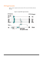
FS2 Target Connection ______________________________________________________ 45
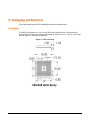
5: Packaging and Electrical ______________________________________ 47
Packaging ________________________________________________________________ 47
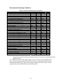
Recommended Circuit Board Layout ____________________________________________ 48
Electrical Specifications ______________________________________________________ 49
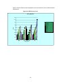
Power Curve Diagrams ______________________________________________________ 53
6: Applications ________________________________________________ 55
Timing ___________________________________________________________________ 56
Data _____________________________________________________________________ 57
Reset ____________________________________________________________________ 58
XTAL ____________________________________________________________________ 59
Burst Flash (3 wire) _________________________________________________________ 60
Burst Flash (2 Wire) _________________________________________________________ 61
Page Flash ________________________________________________________________ 62
Serial Flash _______________________________________________________________ 63
Static RAM ________________________________________________________________ 64
SDRAM __________________________________________________________________ 65
External DMA ______________________________________________________________ 66
ARDY ____________________________________________________________________ 67
PHY (10/100 Mbit) __________________________________________________________ 68
Fibre (100 Mbit) ____________________________________________________________ 69
LED Functionality ___________________________________________________________ 70
7: Instruction Clocks____________________________________________ 71
8: DSTni Sample Code __________________________________________ 85
9: Baud Rate Calculations ______________________________________ 107
iii
List of Figures
Figure 3-1. PLL and Clock Generator ....................................................................................... 37
Figure 4-1. Typical FS2 Target Connection .............................................................................. 45
Figure 5-1. DSTni Package ....................................................................................................... 47
Figure 5-2. Recommended Circuit Board Layout ...................................................................... 48
Figure 5-3. DSTni Current ......................................................................................................... 53
Figure 5-4. DSTni Power Curve ................................................................................................ 54
Figure 6-1. LEDs ....................................................................................................................... 70
List of Tables
Table 2-1. Interrupt Vectors ........................................................................................................ 7
Table 2-2. Interrupt Controller Register Summary..................................................................... 14
Table 2-3. CAN Interrupt Control Register ................................................................................ 15
Table 2-4. CAN Interrupt Control Register Definitions............................................................... 15
Table 2-5. DMA 3 Interrupt Control Register ............................................................................. 15
Table 2-6. DMA 3 Interrupt Control Register Definitions ........................................................... 16
Table 2-7. DMA 2 Interrupt Control Register ............................................................................. 16
Table 2-8. DMA 2 Interrupt Control Register Definitions ........................................................... 16
Table 2-9. Serial Port 3 Interrupt Control Register .................................................................... 16
Table 2-10. Serial Port 3 Interrupt Control Register Definitions ................................................ 17
Table 2-11. Serial Port 0 Interrupt Control Register .................................................................. 17
Table 2-12. Serial Port 0 Interrupt Control Register Definitions ................................................ 17
Table 2-13. Serial Port 1 Interrupt Control Register .................................................................. 17
Table 2-14. Serial Port 1 Interrupt Control Register Definitions ................................................ 18
Table 2-15. Serial Port 2 Interrupt Control Register .................................................................. 18
Table 2-16. Serial Port 2 Interrupt Control Register Definitions ................................................ 18
Table 2-17. INT3 or USB Interrupt Control Register.................................................................. 19
Table 2-18. Serial Port 2 Interrupt Control Register Definitions ................................................ 19
Table 2-19. INT2 (SPI/I2C) Interrupt Control Register ............................................................... 19
Table 2-20. INT2 (SPI/I2C) Interrupt Control Register Definitions ............................................. 20
Table 2-21. INT1 or Ethernet MAC 1 Interrupt Control Register................................................ 21
Table 2-22. INT1 or Ethernet MAC 1 Interrupt Control Register Definitions .............................. 21
Table 2-23. Ethernet MAC 0 (INT0) Interrupt Control Register ................................................. 22
Table 2-24. Ethernet MAC 0 (INT0) Interrupt Control Register Definitions................................ 22
Table 2-25. DMA 1 Interrupt Control Register ........................................................................... 23
Table 2-26. DMA 1 Interrupt Control Register Definitions ......................................................... 23
Table 2-27. DMA 0 Interrupt Control Register ........................................................................... 23
Table 2-28. DMA 0 Interrupt Control Register Definitions ......................................................... 23
Table 2-29. Timer Interrupt Control Register............................................................................. 24
Table 2-30. Timer Interrupt Control Register Definitions ........................................................... 24
Table 2-31. Interrupt Status Register ........................................................................................ 24
Table 2-32. Interrupt Status Register Definitions....................................................................... 24
Table 2-33. Interrupt Request Register ..................................................................................... 25
Table 2-34. Interrupt Request Register Definitions ................................................................... 25
Table 2-35. In-Service Register................................................................................................. 26
Table 2-36. In-Service Register Definitions ............................................................................... 26
Table 2-37. Priority Mask Register ............................................................................................ 27
Table 2-38. Priority Mask Register Definitions .......................................................................... 27
Table 2-39. Interrupt Mask Register.......................................................................................... 28
Table 2-40. Interrupt Mask Register Definitions ........................................................................ 28
Table 2-41. Poll Status Register................................................................................................ 29
Table 2-42. Poll Status Register Definitions .............................................................................. 29
Table 2-43. Poll Register........................................................................................................... 29
Table 2-44. Poll Register Definitions ......................................................................................... 29
Table 2-45. End of Interrupt Register ........................................................................................ 30
Table 2-46. End of Interrupt Register Definitions ...................................................................... 30
Table 3-1. Miscellaneous Register Summary............................................................................ 31
Table 3-2. Checksum Adder Register ....................................................................................... 32
Table 3-3. Checksum Adder Register Definitions...................................................................... 32
iv
Table 3-4. Checksum Data Register ......................................................................................... 32
Table 3-5. Checksum Data Register Definitions........................................................................ 32
Table 3-6. LED Control Register ............................................................................................... 33
Table 3-7. LED Control Register Definitions ............................................................................. 33
Table 3-8. LED Bits [3] and [2] .................................................................................................. 34
Table 3-9. LED Bits [1] and [0] .................................................................................................. 34
Table 3-10. PLL/CLK Control Register...................................................................................... 35
Table 3-11. PLL/CLK Control Register Definitions .................................................................... 35
Table 3-12. Divider Bits and Corresponding Values.................................................................. 36
Table 3-13. Random Number Generator Register .................................................................... 38
Table 3-14. Random Number Generator Register Definitions................................................... 38
Table 3-15. RS/LI Combinations ............................................................................................... 38
Table 4-1. ADDR, DATA, and STAT Scan Chain...................................................................... 40
Table 4-2. STATUS Scan Chain ............................................................................................... 41
Table 4-3. TRACE Buffer .......................................................................................................... 43
Table 4-4. DEICE Instructions................................................................................................... 44
Table 5-1. Absolute Maximum Ratings ..................................................................................... 49
Table 5-2. Recommended Operating Conditions ...................................................................... 50
Table 5-3. I/O Characteristics Xin/Xout Pins ............................................................................ 51
Table 5-4. PHY Receiver Input Characteristics ......................................................................... 51
Table 5-5. 100Base-TX Transceiver Characteristics................................................................. 51
Table 5-6. 100Base-FX Transceiver Characteristics................................................................. 51
Table 5-7. 100Base-T Transceiver Characteristics ................................................................... 52
Table 5-8. 100Base-T Link Integrity Timing Characteristics...................................................... 52
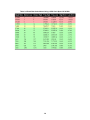
Table 9-1. Baud Rate Calculations Using a CPU Clock Speed of 20 MHz ............................. 107
Table 9-2. Baud Rate Calculations Using a CPU Clock Speed of 24 MHz ............................. 108
Table 9-3. Baud Rate Calculations Using a CPU Clock Speed of 25 MHz ............................. 109
Table 9-4. Baud Rate Calculations Using a CPU Clock Speed of 36 MHz ............................. 109
Table 9-5. Baud Rate Calculations Using a CPU Clock Speed of 48 MHz ............................. 110
Table 9-6. Baud Rate Calculations Using a CPU Clock Speed of 60 MHz ............................. 110
Table 9-7. Baud Rate Calculations Using a CPU Clock Speed of 72 MHz ............................. 111
Table 9-8. Baud Rate Calculations Using a CPU Clock Speed of 84 MHz ............................. 111
Table 9-9. Baud Rate Calculations Using a CPU Clock Speed of 96 MHz ............................. 112
v
1: About This User Guide
This User Guide describes the technical features and programming interfaces of the Lantronix
DSTni-EX chip (hereafter referred to as “DSTni”).
DSTni is an Application Specific Integrated Circuit (ASIC)-based single-chip solution (SCS) that
integrates the leading-edge functionalities needed to develop low-cost, high-performance device
server products. On a single chip, the DSTni integrates an x186 microprocessor, 16K-byte
ROM, 256K-byte SRAM, programmable input/output (I/O), and serial, Ethernet, and Universal
Serial Bus (USB) connectivity — key ingredients for device- server solutions. Although DSTni
embeds multiple functions onto a single chip, it can be easily customized, based on the
comprehensive feature set designed into the chip.
Providing a complete device server solution on a single chip enables system designers to build
affordable, full-function solutions that provide the highest level of performance in both
processing power and peripheral systems, while reducing the number of total system
components. The advantages gained from this synergy include:
Simplifying system design and increased reliability.
Minimizing marketing and administration costs by eliminating the need to source
products from multiple vendors.
Eliminating the compatibility and reliability problems that occur when combining
separate subsystems.
Dramatically reducing implementation costs.
Increasing performance and functionality, while maintaining quality and cost
effectiveness.
Streamlining development by reducing programming effort and debugging time.
Enabling solution providers to bring their products to market faster.
These advantages make DSTni the ideal solution for designs requiring x86 compatibility;
increased performance; serial, programmable I/O, Ethernet, and USB communications; and a
glueless bus interface.
1
Intended Audience
This User Guide is intended for use by hardware and software engineers, programmers, and
designers who understand the basic operating principles of microprocessors and their systems
and are considering designing systems that utilize DSTni.
Conventions
This User Guide uses the following conventions to alert you to information of special interest.
The symbols # and n are used throughout this Guide to denote active LOW signals.
Notes: Notes are information requiring attention.
Navigating Online
The electronic Portable Document Format (PDF) version of this User Guide contains hyperlinks.
Clicking one of these hyper links moves you to that location in this User Guide. The PDF file
was created with Bookmarks and active links for the Table of Contents, Tables, Figures and
cross-references.
2
Organization
This User Guide contains information essential for system architects and design engineers. The
information in this User Guide is organized into the following chapters and appendixes.
Section 1: Introduction
Describes the DSTni architecture, design benefits, theory of operations, ball
assignments, packaging, and electrical specifications. This chapter includes a
DSTni block diagram.
Section 2: Microprocessor
Describes the DSTni microprocessor and its control registers.
Section 2: SDRAM
Describes the DSTni SDRAM and the registers associated with it.
Section 3: Serial Ports
Describes the DSTni serial ports and the registers associated with them.
Section 3: Programmable Input/Output
Describes DSTni’s Programmable Input/ Output (PIO) functions and the
registers associated with them.
Section 3: Timers
Describes the DSTni timers.
Section 4: Ethernet Controllers
Describes the DSTni Ethernet controllers.
Section 4: Ethernet PHY
Describes the DSTni Ethernet physical layer core.
Section 5: SPI Controller
Describes the DSTni Serial Peripheral Interface (SPI) controller.
Section 5: I2C Controller
Describes the DSTni I2C controller.
Section 5: USB Controller
Describes the DSTni USB controller.
Section 5: CAN Controllers
Describes the DSTni Controller Area Network (CAN) bus controllers.
Section 6: Interrupt Controller
Describes the DSTni interrupt controller.
Section 6: Miscellaneous Registers
Describes DSTni registers not covered in other chapters of this Guide.
Section 6: Debugging In-circuit Emulator (Delce)
Section 6: Packaging and Electrical
Describes DSTni’s packaging and electrical characteristics.
Section 6: Applications
Describes DSTni’s packaging and electrical characteristics.
Section 6: Instruction Clocks
Describes the DSTni instruction clocks.
Section 6: DSTni Sample Code
Section 6: Baud Rate Calculations
Provides baud rate calculation tables.
3
2: Interrupt Controller
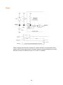
This chapter describes the DSTni interrupt controller. Topics in this chapter include:
Overview on page 6
Theory of Operation on page 7
Interrupt Controller Register Summary on page 14
Register Definitions on page 15
5
Overview
DSTni can receive interrupt requests from a variety of internal and external sources. DSTni’s
internal interrupt controller arranges these requests by priority and presents them one at a time
to the microprocessor.
There are 15 interrupt sources available on DSTni:
The timers use three.
The UARTs use four.
The DMA channels use four.
The peripherals use four:
−
−
−
−
−
INT0 connects to Ethernet MAC 0.
INT1 is Ethernet MAC 1 ORed with external 1.
INT2 connects to both the SPI controller and the I2C controller.
INT3 connects to both the USB controller and an external input
pin.
INT6 is both CAN channels.
Interrupts are automatically disabled when an interrupt is taken. Interrupt-service routines
(ISRs) can re-enable interrupts by setting the IF flag. This allows interrupts of equal or greater
priority to interrupt the currently executing ISR. Interrupts from the same source are disabled so
long as the corresponding bit in the interrupt in-service register is set.
6
Theory of Operation
Interrupt Vector Table
Table 2-1 provides information about the reserved interrupts.
Table 2-1. Interrupt Vectors
Interrupt Name
Vector Type
Vector Address
Default
Priority
Related
Instructions
Divide Error Exception
0
00h
1
DIV, DIV
(See Note 1)
Single Step Interrupt
1
04h
1A
All
(See Note 2)
Non-Maskable (NMI)
2
08h
1
INT
Breakpoint Interrupt
3
0Ch
1
INT
(See Note 1)
INT0 Detected Overflow Exception
4
10h
1
INT0
Array Bounds Exception
5
14h
1
BOUND
(See Note 1)
Unused Opcode Exception
6
18h
1
Undefined
(See Note 1)
Opcodes
ESC Opcode Exception
7
1Ch
1
ESC
(See Note 1)
Time 0 Interrupt
8
20h
2A
(See Note 3)
Reserved
9
24h
DMA 0 Interrupt
10
28h
4
DMA 1 Interrupt
11
2Ch
5
Ethernet MAC 0 (INT0) Interrupt
12
30h
6
INT1 or Ethernet MAC 1 Interrupt
13
34h
7
2
INT2 or SPI/I C Interrupt
14
38h
8
INT3 or USB Interrupt
15
3Ch
9
UART 2 Interrupt
16
40h
10
UART 1 Interrupt
17
44h
15
Timer 1 Interrupt
18
48h
2B
(See Note 3)
Timer 2 Interrupt
19
4Ch
2C
(See Note 3)
UART 0 Interrupt
20
50h
15
INT5 or UART 3 Interrupt
21
54h
11
DMA 2 Interrupt
22
58h
12
DMA 3 Interrupt
23
5Ch
13
CAN Interrupts
24
60h
14
Default priorities for interrupt sources are used only if you do not program each source to a unique priority level.
Note 1. Generated as a result of an instruction execution.
Note 2. Performed the same way as the 8086.
Note 3. All three timers make up a single interrupt request from the interrupt controller and share the same
priority level. However, each timer has a defined priority with respect to the other:
Priority level 2A is the highest, followed by 2B and 2C.
7
Interrupt Type
An 8-bit interrupt type identifies each of the 256 possible interrupts.
Software exceptions, internal peripherals, and non-cascaded external interrupts supply the
interrupt type through the internal interrupt controller.
Cascaded external interrupts and slave-mode external interrupts get the interrupt type from the
external interrupt controller by means of interrupt acknowledge cycles on the bus.
Interrupt Vector Table
The interrupt vector table is a 1K memory area that starts at address 00000h. It has up to 256
four-byte address pointers containing the address for the interrupt service routine for each
possible interrupt type. For each interrupt, an 8-bit interrupt type identifies the appropriate
interrupt vector table entry.
Interrupts 00h to 5Ch are reserved (see Table 2-1 on page 7).
The microprocessor calculates the index to the interrupt vector table by shifting the interrupt
type left two bits (multiplying by 4).
Maskable/Nonmaskable Interrupts
Interrupt types 08h through 1Fh are maskable. Of these, only 08h through 14h are actually used
(see Table 2-1 on page 7) The maskable interrupts are enabled and disabled by the interrupt
enable flag (IF) in the microprocessor status flags; however, the INT command can execute any
interrupt regardless of the setting of IF.
Interrupt types 00h through 07h and all software interrupts (the INT instruction) are
nonmaskable. The nonmaskable interrupts are not affected by the setting of the IF flag.
DSTni provide two ways to mask and unmask maskable interrupt sources.
Each interrupt source has an interrupt control register that contains a mask bit
specific to that interrupt.
In addition, the interrupt mask register is provided as a single source to access all of the
mask bits.
If the interrupt mask register is written while interrupts are enabled, an interrupt can occur while
the register is in an undefined state. This can cause interrupts to be accepted even though they
were masked before and after the write to the interrupt mask register. As a result, the interrupt
mask register should only be written when interrupts are disabled. Mask bits in the individual
interrupt control registers can be written while interrupts are enabled, without erroneous
interrupt operation.
Interrupt Enable Flag
The interrupt enable flag (IF) is part of the microprocessor status flags.
If IF = 1, maskable interrupts are enabled and can cause microprocessor interrupts.
(Individual maskable interrupts can still be disabled by means of the mask bit in each
control register.)
If IF = 0, all maskable interrupts are disabled.
The IF flag does not affect the NMI or software exception interrupts (interrupt types 00h to 07h)
or the execution of any interrupt through the INT instruction.
Interrupt Mask Bit
Each interrupt control register for the maskable interrupts contains a mask bit (MSK).
If MSK = 1 for a particular interrupt, that interrupt is disabled, regardless of the IF setting.
8
Interrupt Priority
The column titled Default Priority in Table 2-1 on page 7 shows the priority for the interrupts at
power-on reset. The nonmaskable interrupts 00h through 07h are always prioritized ahead of
the maskable interrupts.
To reprioritize the maskable interrupts, reconfigure the PR2–PR0 bits in the interrupt control
registers. The PR2–PR0 bits in all the maskable interrupts are set to priority level 7 at power-on
reset.
Software Interrupts
Software interrupts can be initiated by the INT instruction. Any of the 256 possible interrupts can
be initiated by the INT instruction.
INT 21h causes an interrupt to the vector located at 00084h in the interrupt vector table.
INT FFh causes an interrupt to the vector located at 003FCh in the interrupt vector
table.
Software interrupts are not maskable and are not affected by the setting of the IF flag.
Software Exceptions
A software exception interrupt occurs when an instruction causes an interrupt due to a condition
in the microprocessor. Interrupt types 00h, 01h, 03h, 04h, 05h, 06h, and 07h are software
exception interrupts.
Software exceptions are not maskable and are not affected by the setting of the IF flag.
Interrupt Conditions and Sequence
The following sections describe how interrupts are serviced.
Nonmaskable Interrupts
The following nonmaskable interrupts are serviced, regardless of the setting of the interrupt
enable flag (IF) in the microprocessor status flags.
The trace interrupt
The NMI interrupt
Software interrupts, both user-defined (INT) and software exceptions.
9
Maskable Hardware Interrupts
For maskable hardware interrupt requests to be serviced:
The STI instruction must set the IF flag must be set, and
The mask bit associated with each interrupt must be reset
Interrupt Request
When an interrupt is requested, DSTni’s internal interrupt controller verifies that the interrupt is
enabled and that there are no higher priority interrupt requests being serviced or pending.
If the interrupt request is granted, the interrupt controller uses the interrupt type to access a
vector from the interrupt vector table (see Table 2-1 on page 7).
Each interrupt type has a four-byte vector available in the interrupt vector table. The interrupt
vector table is located in the 1024 bytes from 00000h to 003FFh. Each four-byte vector consists
of a 16-bit offset (IP) value and a 16-bit segment (CS) value. The 8-bit interrupt type is shifted
left 2 bit positions (multiplied by 4) to generate the index into the interrupt vector table.
Interrupt Servicing
A valid interrupt transfers execution to a new program location based on the vector in the
interrupt vector table. The next instruction address (CS:IP) and the microprocessor status flags
are pushed onto the stack.
The interrupt enable flag (IF) clears after the microprocessor status flags are pushed on the
stack, disabling maskable interrupts during the interrupt service routine (ISR).
The segment:offset values from the interrupt vector table are loaded into the code segment
(CS) and the instruction pointer (IP), and execution of the ISR begins.
Returning from an Interrupt
The interrupt return (IRET) instruction pushes the microprocessor status flags and the return
address off the stack. Program execution resumes at the point where the interrupt occurred.
The interrupt enable flag (IF) is restored by the IRET instruction along with the remaining
microprocessor status flags. If the IF flag was set before the interrupt was serviced, interrupts
are re-enabled when the IRET is executed. If there are valid interrupts pending when the IRET
is executed, the instruction at the return address is not executed. Instead, the new interrupt is
serviced immediately.
If an ISR intends to modify the value of any of the saved flags permanently, it must modify the
copy of the microprocessor status flags register that was pushed onto the stack.
10
Interrupt Priority
Table 2-1 on page 7 shows DSTni’s predefined interrupt types and default priority structure.
Nonmaskable interrupts (interrupt types 0–7) always have a higher priority than maskable
interrupts. However, maskable interrupts have a programmable priority that can override the
default priorities relative to one another.
The levels of interrupt priority are:
Interrupt priority for nonmaskable interrupts and software interrupts
Interrupt priority for maskable hardware interrupts
Nonmaskable Interrupts and Software Interrupt Priority
The nonmaskable interrupts from 00h to 07h and software interrupts (INT instruction) always
take priority over the maskable hardware interrupts. Within the nonmaskable and software
interrupts, the trace interrupt has the highest priority, followed by the NMI interrupt, and the
remaining nonmaskable and software interrupts.
After the trace interrupt and the NMI interrupt, the remaining software exceptions are mutually
exclusive and can only occur one at a time, obviating the need for a further priority breakdown.
Maskable Hardware Interrupt Priority
Starting with interrupt type 8 (timer 0 interrupt), the maskable hardware interrupts have both a
default priority (see Table 2-1 on page 7) and a programmable priority. The programmable
priority is the primary priority for maskable hardware interrupts. The overall priority is the
secondary priority for maskable hardware interrupts.
Since all maskable interrupts are set to a programmable priority of seven on reset, the overall
priority of the interrupts determines the priority in which each interrupt is granted by the interrupt
controller until programmable priorities are changed by reconfiguring the control registers.
The default priority levels shown in Table 2-1 on page 7 are not the same as the programmable
priority level associated with each maskable hardware interrupt. Each of the maskable hardware
interrupts has a programmable priority from 0 to 7, with 0 being the highest priority (see Table
2-1 on page 7).
For example, if the INT4–INT0 interrupts are all changed to programmable priority 6 and no
other programmable priorities are changed from the reset value of seven, the INT4–INT0
interrupts take precedence over all other maskable interrupts. (Within INT4–INT0, the hierarchy
is as follows: INT0>INT1>INT2>INT3>INT4.)
Software Exceptions, Traps, and NMI
The following predefined interrupts cannot be masked by programming.
Divide Error Exception (Interrupt Type 00h)
Generated when a DIV or IDIV instruction quotient cannot be expressed in the number of
destination bits.
Trace Interrupt (Interrupt Type 01h)
If the trace flag (TF) in the microprocessor status flags register is set, the trace interrupt is
generated after most instructions. This interrupt lets program execute in single-step mode. The
interrupt is not generated after prefix instructions like REP, instructions that modify segment
registers like POP DS, or the WAIT instruction.
Taking the trace interrupt clears the TF bit after the microprocessor status flags are pushed onto
the stack. The IRET instruction at the end of the single step interrupt service routine restores
the microprocessor status flags (and the TF bit) and transfers control to the next instruction to
be traced.
Trace mode is initiated by pushing the microprocessor status flags onto the stack, then setting
the TF flag on the stack, and then popping the flags.
11
Nonmaskable Interrupt-NMI (Interrupt Type 02h)
This pin tells DSTni that an interrupt request has occurred. The NMI signal is the highest priority
hardware interrupt and, unlike the INT4–INT0 pins, cannot be
masked. DSTni always transfers program execution to the location specified by the
nonmaskable interrupt vector in the DSTni interrupt vector table when NMI is asserted.
Although NMI is the highest priority interrupt source, it does not participate in the priority
resolution process of the maskable interrupts. There is no bit associated with NMI in the
interrupt in-service or interrupt request registers. This means that a new NMI request can
interrupt an executing NMI interrupt service routine. As with all hardware interrupts, the IF
(interrupt flag) clears when the microprocessor takes the interrupt, disabling the maskable
interrupt sources. However, if maskable interrupts are re-enabled by software in the NMI
interrupt service routine (via the STI instruction, for example), the NMI currently in service does
not affect the priority resolution of maskable interrupt requests. For this reason, the NMI
interrupt service routine should not enable the maskable interrupts.
Breakpoint Interrupt (Interrupt Type 03h)
An interrupt caused by the 1-byte version of the INT instruction (INT3).
INT0 Detected Overflow Exception (Interrupt Type 04h)
Generated by an INT0 instruction if the OF bit is set in the Processor Status Flags (F) register.
Array BOUNDS Exception (Interrupt Type 05h)
Generated by a BOUND instruction if the array index is outside the array bounds. The array
bounds are located in memory at a location indicated by one of the instruction operands.
The other operand indicates the value of the index to be checked.
Unused Opcode Exception (Interrupt Type 06h)
Generated if execution is attempted on undefined opcodes.
ESC Opcode Exception (Interrupt Type 07h)
Generated if execution of ESC opcodes (D8h–DFh) is attempted. DSTni does not check the
escape opcode trap bit. The return address of this exception points to the ESC instruction that
caused the exception. If a segment override prefix preceded the ESC instruction, the return
address points to the segment override prefix.
Note: All numeric coprocessor opcodes cause a trap. DSTni does not support the numeric
coprocessor interface.
12
Interrupt Acknowledge
Interrupts can be acknowledged in two different ways:
The internal interrupt controller can provide the interrupt type.
An external interrupt controller can provide the interrupt type.
The microprocessor requires the interrupt type as an index into the interrupt vector table. When
the internal interrupt controller is supplying the interrupt type, no interrupt acknowledge bus
cycles are generated. The only external indication that an interrupt is being serviced is the
microprocessor reading the interrupt vector table.
When an external interrupt controller supplies the interrupt type, the microprocessor generates
two interrupt acknowledge bus cycles. The external interrupt controller writes the interrupt type
to the AD7–AD0 lines during the second bus cycle.
Interrupt acknowledge bus cycles have the following characteristics:
The two interrupt acknowledge cycles are locked.
Two idle states are always inserted between the two interrupt acknowledge cycles.
Wait states are inserted if READY is not returned to the microprocessor.
Interrupt Controller Reset Conditions
On reset, the interrupt controller performs the following actions:
1.
2.
All special fully nested mode (SFNM) bits are reset, implying fully nested mode.
All priority (PR) bits in the various control registers are set to 1. This places all sources at
the lowest priority (level 7).
3.
All level-triggered mode (LTM) bits are reset to 0, resulting in edge-triggered mode.
4.
All interrupt in-service bits are reset to 0.
5.
All interrupt request bits are reset to 0.
6.
All mask (MSK) bits are set to 1. All interrupts are masked.
7.
All cascade (C) bits are reset to 0 (non-cascade).
8.
The interrupt priority mask is set to 7, permitting interrupts of all priorities.
9.
The interrupt controller is initialized to master mode.
Polled Environments
The interrupt controller can be used in polled mode if interrupts are not desired. When polling,
interrupts are disabled and software polls the interrupt controller as required. The interrupt
controller is polled by reading the Poll Status register (see Poll Status Register on page 29).
Bit [15] indicates to the microprocessor that an interrupt of high enough priority is
requesting service.
Bits [4:0] indicate to the microprocessor the interrupt type of the highest-priority source
requesting service.
After determining that an interrupt is pending, software reads the Poll register (see Poll Register
on page 29), which causes the in-service bit of the highest-priority source to be set.
To enable reading of the Poll register information without setting the indicated in-service bit,
DSTni provides a Poll Status register in addition to the Poll register. The Poll Status register
contains the same information in the Poll register; however the Poll Status register can be read
without setting the associated in-service bit. These registers are located in two adjacent
memory locations in the peripheral control block.
13
End-of-Interrupt Write to the EOI Register
When an interrupt service routine completes, a program must write to the EOI register to reset
the in-service (IS) bit. There are two types of writes to the EOI register — specific EOI and nonspecific EOI (see End-of-Interrupt Write to the EOI Register on page 14).
Non-specific EOI does not specify which IS bit is to be reset. Instead, the interrupt controller
automatically resets the IS bit of the highest priority source with an active service routine.
Specific EOI requires the program to send the interrupt type to the interrupt controller to indicate
the source IS bit that is to be reset. Specific reset is applicable when interrupt nesting is
possible or when the highest priority IS bit that was set does not belong to the service routine in
progress.
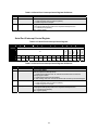
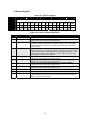
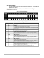
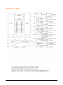
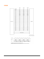
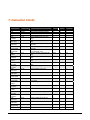
Interrupt Controller Register Summary
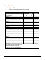
Table 2-2. Interrupt Controller Register Summary
Hex Offset
4C
4A
48
46
44
42
40
3E
3C
3A
38
36
34
32
30
2E
2C
2A
28
26
24
22
Description
Page
CAN Interrupt Control register
DMA 3 Interrupt Control register
DMA 2 Interrupt Control register
Serial Port 3 Interrupt Channel register
Serial Port 0 Interrupt Channel register
Serial Port 1 Interrupt Channel register
Serial Port 2 Interrupt Channel register
INT3 or USB Interrupt Control register
INT2 (SPI/I2C) Interrupt Control register
INT1 or Ethernet MAC 1 Interrupt Control register
Ethernet MAC 0 (INT0) Interrupt Control register
DMA 1 Interrupt Control register
DMA 0 Interrupt Control register
Timer Interrupt Control register
Interrupt Status register
Interrupt Request register
In-Service register
Priority Mask register
Interrupt Mask register
Poll Status register
Poll register
End of Interrupt (EOI) register
14
15
15
16
16
17
17
18
19
19
21
22
23
23
23
24
25
26
27
28
29
29
30
Register Definitions
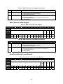
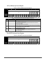
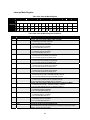
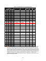
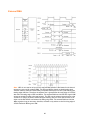
CAN Interrupt Control Register
12
11
10
9
8
7
6
5
4
3
2
1
0
PR0
13
PR1
14
PR2
15
MSK
BIT
OFFSET
LTM
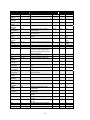
Table 2-3. CAN Interrupt Control Register
0
R
W
0
R
W
0
R
W
0
RW
1
R
W
1
R
W
1
R
W
1
R
W
4Ch
FIELD
///
RESET
RW
0
R
W
0
RW
0
R
W
0
RW
0
RW
0
RW
0
RW
0
R
W
Table 2-4. CAN Interrupt Control Register Definitions
Bits
Field Name
15:5
4
LTM
3
MSK
2:0
PR[2:0]
Description
Reserved
Level Trigger Mode
Sets the respective interrupt source.
1 = enable level-triggered mode. An interrupt generates when the external
interrupt signal is HIGH.
0 = enable edge-triggered mode (default).
For both settings, the level must remain HIGH until the interrupt is acknowledged.
Mask Interrupt
1 = mask respective interrupt request (default)
0 = enable respective interrupts.
Programmable Priority Level
The programmable priority level for the respective interrupt source.
111 = lowest priority.(default)
000 = highest priority.
\\\
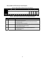
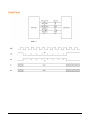
DMA 3 Interrupt Control Register
13
12
11
10
9
8
7
6
5
4
0
R
W
0
R
W
0
R
W
0
RW
2
1
0
1
R
W
1
R
W
1
R
W
1
R
W
4Ah
FIELD
///
RESET
RW
3
PR0
14
PR1
15
PR2
BIT
OFFSET
MSK
Table 2-5. DMA 3 Interrupt Control Register
0
R
W
0
RW
0
R
W
0
RW
0
RW
0
RW
0
RW
0
R
W
15
Table 2-6. DMA 3 Interrupt Control Register Definitions
Bits
Field Name
15:4
3
MSK
2:0
PR[2:0]
Description
Reserved
Mask Interrupt
1 = mask respective interrupt request (default)
0 = enable respective interrupts.
Programmable Priority Level
The programmable priority level for the respective interrupt source.
111 = lowest priority.(default)
000 = highest priority.
\\\
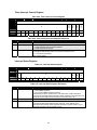
DMA 2 Interrupt Control Register
BIT
OFFSET
15
14
13
12
11
10
9
8
7
6
5
4
0
R
W
0
R
W
0
R
W
0
RW
3
2
1
0
MSK
Table 2-7. DMA 2 Interrupt Control Register
1
R
W
48h
0
RW
0
R
W
0
RW
0
RW
0
RW
0
RW
0
R
W
PR0
0
R
W
PR1
RESET
RW
PR2
FIELD
1
R
W
1
R
W
1
R
W
Table 2-8. DMA 2 Interrupt Control Register Definitions
Bits
Field Name
15:4
3
MSK
2:0
PR[2:0]
Description
Reserved
Mask Interrupt
1 = mask respective interrupt request (default)
0 = enable respective interrupts.
Programmable Priority Level
The programmable priority level for the respective interrupt source.
111 = lowest priority.(default)
000 = highest priority.
\\\
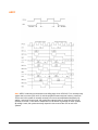
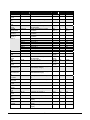
Serial Port 3 Interrupt Control Register
12
11
10
9
8
7
6
5
4
3
2
1
0
PR0
13
PR1
14
PR2
15
MSK
BIT
OFFSET
LTM
Table 2-9. Serial Port 3 Interrupt Control Register
0
R
W
0
R
W
0
R
W
0
RW
1
R
W
1
R
W
1
R
W
1
R
W
46h
FIELD
///
RESET
RW
0
R
W
0
RW
0
R
W
0
RW
0
RW
0
RW
0
RW
0
R
W
16
Table 2-10. Serial Port 3 Interrupt Control Register Definitions
Bits
Field Name
15:5
4
LTM
3
MSK
2:0
PR[2:0]
Description
Reserved
Level Trigger Mode
Sets the respective interrupt source.
1 = enable level-triggered mode. An interrupt generates when the external
interrupt signal is HIGH.
0 = enable edge-triggered mode (default).
For both settings, the level must remain HIGH until the interrupt is acknowledged.
Mask Interrupt
1 = mask respective interrupt request (default)
0 = enable respective interrupts.
Programmable Priority Level
The programmable priority level for the respective interrupt source.
111 = lowest priority.(default)
000 = highest priority.
\\\
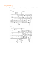
Serial Port 0 Interrupt Control Register
15
14
13
12
11
10
9
8
7
6
5
4
0
R
W
0
R
W
0
R
W
0
RW
2
1
0
0
R
W
0
RW
0
R
W
0
RW
0
RW
0
RW
0
RW
0
R
W
1
R
W
PR0
///
PR1
FIELD
RESET
RW
3
44h
PR2
BIT
OFFSET
MSK
Table 2-11. Serial Port 0 Interrupt Control Register
1
R
W
1
R
W
1
R
W
Table 2-12. Serial Port 0 Interrupt Control Register Definitions
Bits
Field Name
15:4
3
MSK
2:0
PR[2:0]
Description
Reserved
Mask Interrupt
1 = mask respective interrupt request (default)
0 = enable respective interrupts.
Programmable Priority Level
The programmable priority level for the respective interrupt source.
111 = lowest priority.(default)
000 = highest priority.
\\\
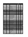
Serial Port 1 Interrupt Control Register
13
12
11
10
9
8
7
6
5
4
0
R
W
0
R
W
0
R
W
0
RW
2
1
0
1
R
W
1
R
W
1
R
W
1
R
W
42h
FIELD
///
RESET
RW
3
PR0
14
PR1
15
PR2
BIT
OFFSET
MSK
Table 2-13. Serial Port 1 Interrupt Control Register
0
R
W
0
RW
0
R
W
0
RW
0
RW
0
RW
0
RW
0
R
W
17
Table 2-14. Serial Port 1 Interrupt Control Register Definitions
Bits
Field Name
15:4
3
MSK
2:0
PR[2:0]
Description
Reserved
Mask Interrupt
1 = mask respective interrupt request (default)
0 = enable respective interrupts.
Programmable Priority Level
The programmable priority level for the respective interrupt source.
111 = lowest priority.(default)
000 = highest priority.
\\\
Serial Port 2 Interrupt Control Register
12
11
10
9
8
7
6
5
4
3
2
1
0
PR0
13
PR1
14
PR2
15
MSK
BIT
OFFSET
LTM
Table 2-15. Serial Port 2 Interrupt Control Register
0
R
W
0
R
W
0
R
W
0
RW
1
R
W
1
R
W
1
R
W
1
R
W
40h
FIELD
///
RESET
RW
0
R
W
0
RW
0
R
W
0
RW
0
RW
0
RW
0
RW
0
R
W
Table 2-16. Serial Port 2 Interrupt Control Register Definitions
Bits
Field Name
15:5
4
\\\
LTM
3
MSK
2:0
PR[2:0]
Description
Reserved
Level Trigger Mode
Sets the respective interrupt source.
1 = enable level-triggered mode. An interrupt generates when the external
interrupt signal is HIGH.
0 = enable edge-triggered mode (default).
For both settings, the level must remain HIGH until the interrupt is acknowledged.
Mask Interrupt
1 = mask respective interrupt request (default)
0 = enable respective interrupts.
Programmable Priority Level
The programmable priority level for the respective interrupt source.
111 = lowest priority.(default)
000 = highest priority.
18
INT3 or USB Interrupt Control Register
12
11
10
9
8
7
6
5
4
3
2
1
0
PR0
13
PR1
14
PR2
15
MSK
BIT
OFFSET
LTM
Table 2-17. INT3 or USB Interrupt Control Register
0
R
W
0
R
W
0
R
W
0
RW
1
R
W
1
R
W
1
R
W
1
R
W
3Eh
FIELD
///
RESET
RW
0
R
W
0
RW
0
R
W
0
RW
0
RW
0
RW
0
RW
0
R
W
Table 2-18. Serial Port 2 Interrupt Control Register Definitions
Bits
Field Name
15:5
4
LTM
3
MSK
2:0
PR[2:0]
Description
Reserved
Level Trigger Mode
Sets the respective interrupt source.
1 = enable level-triggered mode. An interrupt generates when the external
interrupt signal is HIGH.
0 = enable edge-triggered mode (default).
For both settings, the level must remain HIGH until the interrupt is acknowledged.
Mask Interrupt
1 = mask respective interrupt request (default)
0 = enable respective interrupts.
Programmable Priority Level
The programmable priority level for the respective interrupt source.
111 = lowest priority.(default)
000 = highest priority.
\\\
INT2 (SPI/I2C) Interrupt Control Register
Table 2-19. INT2 (SPI/I2C) Interrupt Control Register
BIT
OFFSET
15
14
13
12
11
10
9
8
7
6
5
4
3
2
1
0
3Ch
RESET
RW
PR0
PR1
PR2
LTM
///
MSK
FIELD
0
0
0
0
0
0
0
0
0
0
0
0
1
1
1
1
RW
RW
RW
RW
RW
RW
RW
RW
RW
RW
RW
RW
RW
RW
RW
RW
19
Table 2-20. INT2 (SPI/I2C) Interrupt Control Register Definitions
Bits
Field Name
15:5
4
\\\
LTM
3
MSK
2:0
PR[2:0]
Description
Reserved
Level Trigger Mode
Sets the respective interrupt source.
1 = enable level-triggered mode. An interrupt generates when the external
interrupt signal is HIGH.
0 = enable edge-triggered mode (default).
For both settings, the level must remain HIGH until the interrupt is acknowledged.
Mask Interrupt
1 = mask respective interrupt request (default)
0 = enable respective interrupts.
Programmable Priority Level
The programmable priority level for the respective interrupt source.
111 = lowest priority.(default)
000 = highest priority.
20
INT1 or Ethernet MAC 1 Interrupt Control Register
Table 2-21. INT1 or Ethernet MAC 1 Interrupt Control Register
BIT
OFFSET
15
14
13
12
11
10
9
8
7
6
5
4
3
2
1
0
3Ah
LTM
MSK
PR2
PR1
PR0
FIELD
0
0
0
0
0
0
0
0
0
0
0
0
1
1
1
1
RW
RW
RW
RW
RW
RW
RW
RW
RW
RW
RW
RW
RW
RW
RW
RW
///
RESET
RW
Table 2-22. INT1 or Ethernet MAC 1 Interrupt Control Register Definitions
Bits
Field Name
15:5
4
\\\
LTM
3
MSK
2:0
PR[2:0]
Description
Reserved
Level Trigger Mode
Sets the respective interrupt source.
1 = enable level-triggered mode. An interrupt generates when the external
interrupt signal is HIGH.
0 = enable edge-triggered mode (default).
For both settings, the level must remain HIGH until the interrupt is acknowledged.
Mask Interrupt
1 = mask respective interrupt request (default)
0 = enable respective interrupts.
Programmable Priority Level
The programmable priority level for the respective interrupt source.
111 = lowest priority.(default)
000 = highest priority.
21
Ethernet MAC 0 (INT0) Interrupt Control Register
Table 2-23. Ethernet MAC 0 (INT0) Interrupt Control Register
BIT
OFFSET
15
14
13
12
11
10
9
8
7
6
5
4
3
2
1
0
38h
LTM
MSK
PR2
PR1
PR0
FIELD
0
0
0
0
0
0
0
0
0
0
0
0
1
1
1
1
RW
RW
RW
RW
RW
RW
RW
RW
RW
RW
RW
RW
RW
RW
RW
RW
///
RESET
RW
Table 2-24. Ethernet MAC 0 (INT0) Interrupt Control Register Definitions
Bits
Field Name
15:5
4
\\\
LTM
3
MSK
2:0
PR[2:0]
Description
Reserved
Level Trigger Mode
Sets the respective interrupt source.
1 = enable level-triggered mode. An interrupt generates when the external
interrupt signal is HIGH.
0 = enable edge-triggered mode (default).
For both settings, the level must remain HIGH until the interrupt is acknowledged.
Mask Interrupt
1 = mask respective interrupt request (default)
0 = enable respective interrupts.
Programmable Priority Level
The programmable priority level for the respective interrupt source.
111 = lowest priority.(default)
000 = highest priority.
22
DMA 1 Interrupt Control Register
BIT
OFFSET
15
14
13
12
11
10
9
8
7
6
5
4
0
R
W
0
R
W
0
R
W
0
RW
3
2
1
0
MSK
Table 2-25. DMA 1 Interrupt Control Register
1
R
W
36h
0
RW
0
R
W
0
RW
0
RW
0
RW
0
RW
0
R
W
PR0
0
R
W
PR1
RESET
RW
PR2
FIELD
1
R
W
1
R
W
1
R
W
Table 2-26. DMA 1 Interrupt Control Register Definitions
Bits
Field Name
15:4
3
MSK
2:0
PR[2:0]
Description
Reserved
Mask Interrupt
1 = mask respective interrupt request (default)
0 = enable respective interrupts.
Programmable Priority Level
The programmable priority level for the respective interrupt source.
111 = lowest priority.(default)
000 = highest priority.
\\\
DMA 0 Interrupt Control Register
13
12
11
10
9
8
7
6
5
4
0
R
W
0
R
W
0
R
W
0
RW
3
2
1
0
PR0
14
PR1
15
PR2
BIT
OFFSET
MSK
Table 2-27. DMA 0 Interrupt Control Register
1
R
W
1
R
W
1
R
W
1
R
W
34h
FIELD
RESET
RW
0
R
W
0
RW
0
R
W
0
RW
0
RW
0
RW
0
RW
0
R
W
Table 2-28. DMA 0 Interrupt Control Register Definitions
Bits
Field Name
15:4
3
\\\
MSK
2:0
PR[2:0]
Description
Reserved
Mask Interrupt
1 = mask respective interrupt request (default)
0 = enable respective interrupts.
Programmable Priority Level
The programmable priority level for the respective interrupt source.
111 = lowest priority.(default)
000 = highest priority.
23
Timer Interrupt Control Register
BIT
OFFSET
15
14
13
12
11
10
9
8
7
6
5
4
0
R
W
0
R
W
0
R
W
0
RW
3
2
1
0
MSK
Table 2-29. Timer Interrupt Control Register
1
R
W
32h
0
R
W
0
RW
0
R
W
0
RW
0
RW
0
RW
0
RW
0
R
W
PR0
RESET
RW
PR1
///
PR2
FIELD
1
R
W
1
R
W
1
R
W
1
0
Table 2-30. Timer Interrupt Control Register Definitions
Bits
Field Name
15:4
3
MSK
2:0
PR[2:0]
Description
Reserved
Mask Interrupt
1 = mask respective interrupt request (default)
0 = enable respective interrupts.
Programmable Priority Level
The programmable priority level for the respective interrupt source.
111 = lowest priority.(default)
000 = highest priority.
\\\
Interrupt Status Register
Table 2-31. Interrupt Status Register
RESET
RW
14
13
12
11
10
9
8
7
6
5
4
3
2
IRT0
///
IRT1
30h
IRT2
FIELD
15
DHL
T
BIT
OFFSET
0
0
0
0
0
0
0
0
0
0
0
0
1
1
1
1
RW
RW
RW
RW
RW
RW
RW
RW
RW
RW
RW
RW
RW
RW
RW
RW
Table 2-32. Interrupt Status Register Definitions
Bits
Field Name
Description
15
DHLT
14:3
2:0
IRT[2:0]
Halt DMA Operations
1 = halt all DMA operations.
0 = do not halt all DMA operations (default).
Automatically set when an NMI occurs, and resets when an IRET instruction
executes. By suspending DMA operations during an NMI, the microprocessor can
quickly service the NMI request. Programmers can also set this bit.
Reserved
Timer Interrupt Request Bits
Lets software differentiate between timer interrupts, as the TMR bit in the
Interrupt Request register is the logical OR of all timer requests. Setting any of
these bits generates a timer-interrupt request.
\\\
24
Interrupt Request Register
Table 2-33. Interrupt Request Register
BIT
OFFSET
FIELD
RESET
RW
15
14
13
12
11
10
9
8
7
6
5
4
3
2
1
0
I3
I2
I1
I0
D1
D0
///
TMR
0
R
W
0
R
W
0
R
W
0
R
W
0
R
W
0
R
W
0
R
W
0
R
2Eh
///
I6
D3
D2
0
R
W
0
R
W
0
R
W
0
R
W
SP
3
0
R
W
SP
0
0
R
W
SP
1
0
R
W
SP
2
0
R
W
Table 2-34. Interrupt Request Register Definitions
Bits
Field Name
15
14
\\\
I6
13:12
D[3:0]
11:8
SP[3:0]
7
I3
6
I2
5
I1
4
I0
3:2
1
0
D[1:0]
///
TMR
Description
Reserved
Logical “OR” Connected to Both CAN0 and CAN1
This bit is the in-service bit for this interrupt source.
Interrupt Request Bits for the DMA Channels (DMA3:0)
Setting any of these bits generates an interrupt request on the corresponding
DMA channel interrupt request line. Resetting any of these bits removes the
interrupt request.
State of the Asynchronous Serial Port Interrupt Requests
These bits are set when the respective serial port generates an interrupt request.
These bits clear when the respective interrupt acknowledge cycle occurs. D3:0
In-service bits for DMA channels DMA3:0. I0 Logical “OR” connected to both
internal MACs. This bit is the in-service bit.
Logical “OR” Connected to External Interrupt 3 and the USB Controller
This bit is the in-service bit for this interrupt source.
Logical “OR” Connected to the SPI Controller and the I2C Controller
This bit is the in-service bit for this interrupt source.
Logical “OR” Connected to External Interrupt 1 and Ethernet MAC 1
This bit is the in-service bit for this interrupt source.
Ethernet MAC 0
This bit is the in-service bit for this interrupt source.
In-Service Bits for DMA Channels DMA1:0
Reserved
Logical OR of All Timer Interrupt Requests
The individual timer interrupt request bits are contained in the interrupt status
register. This bit cannot be written.
25
In-Service Register
Table 2-35. In-Service Register
BIT
OFFSET
FIELD
RESET
RW
15
14
13
12
11
10
9
8
7
6
5
4
3
2
1
0
I3
I2
I1
I0
D1
D0
///
TMR
0
R
W
0
R
W
0
R
W
0
R
W
0
R
W
0
R
W
0
R
W
0
RW
2Ch
///
I6
D3
D2
0
R
W
0
R
W
0
R
W
0
R
W
SP
3
0
R
W
SP
0
0
R
W
SP
1
0
R
W
SP
2
0
R
W
Table 2-36. In-Service Register Definitions
Bits
Field Name
15
14
\\\
I6
13:12
D[3:0]
11:8
SP[3:0]
7
I3
6
I2
5
I1
4
I0
3:2
1
0
D[1:0]
///
TMR
Description
Reserved
Logical “OR” Connected to Both CAN0 and CAN1
This bit is the in-service bit for this interrupt source.
Interrupt Request Bits for the DMA Channels (DMA3:0)
Setting any of these bits generates an interrupt request on the corresponding
DMA channel interrupt request line. Resetting any of these bits removes the
interrupt request.
State of the Asynchronous Serial Port Interrupt Requests
These bits are set when the respective serial port generates an interrupt request.
These bits clear when the respective interrupt acknowledge cycle occurs. D3:0
In-service bits for DMA channels DMA3:0. I0 Logical “OR” connected to both
internal MACs. This bit is the in-service bit.
Logical “OR” Connected to External Interrupt 3 and the USB Controller
This bit is the in-service bit for this interrupt source.
Logical “OR” Connected to the SPI Controller and the I2C Controller
This bit is the in-service bit for this interrupt source.
Logical “OR” Connected to External Interrupt 1 and Ethernet MAC 1
This bit is the in-service bit for this interrupt source.
Ethernet MAC 0
This bit is the in-service bit for this interrupt source.
In-Service Bits for DMA Channels DMA1:0
Reserved
Logical OR of All Timer Interrupt Requests
The individual timer interrupt request bits are contained in the interrupt status
register. This bit cannot be written.
26
Priority Mask Register
Table 2-37. Priority Mask Register
BIT
OFFSET
15
14
13
12
11
10
9
8
7
6
5
4
3
2
1
0
2Ah
FIELD
PR0
RW
PR1
RESET
PR2
///
0
0
0
0
0
0
0
0
0
0
0
0
0
1
1
1
RW
RW
RW
RW
RW
RW
RW
RW
RW
RW
RW
RW
RW
RW
RW
RW
Table 2-38. Priority Mask Register Definitions
Bits
Field Name
15:3
2:1
\\\
PR[2:1]
0
TMR
Description
Reserved
Minimum Priority Level an Interrupt Request Must Have to be Recognized
An interrupt request is processed by the interrupt controller if its priority level is
greater than or equal to the priority in this register.
111 = lowest priority (default).
000 = highest priority.
Logical OR of All Timer Interrupt Requests
The individual timer interrupt request bits are contained in the interrupt status
register. This bit cannot be written.
27
Interrupt Mask Register
Table 2-39. Interrupt Mask Register
BIT
OFFSET
FIELD
RESET
RW
15
14
13
12
11
10
9
8
7
6
5
4
3
2
1
0
I3
I2
I1
I0
D1
D0
///
TMR
1
R
W
1
R
W
1
R
W
1
R
W
1
R
W
1
R
W
0
RW
1
RW
28h
///
I6
D3
D2
1
R
W
1
R
W
1
R
W
1
R
W
SP
3
1
R
W
SP
0
1
R
W
SP
1
1
R
W
SP
2
1
R
W
Table 2-40. Interrupt Mask Register Definitions
Bits
Field Name
15
14
\\\
I6
13
D3
12
D2
11
SP3
10
SP0
9
SP1
8
SP2
7
I3
6
I2
5
I1
4
I0
3
D1
2
D0
1
0
TMR
///
Description
Reserved
Logical “OR” Connected to Both CAN0 and CAN1
1 = mask CAN 0 and CAN 1 (default).
0 = do not mask CAN 0 and CAN 1.
Mask DMA Channel 3 Interrupt
1 = mask DMA channel 3 (default).
0 = do not mask DMA channel 3.
Mask DMA Channel 2 Interrupt
1 = mask DMA channel 2 (default).
0 = do not mask DMA channel 2.
Asynchronous Serial Port 3
1 = mask asynchronous serial port 3 (default).
0 = do not mask asynchronous serial port 3.
Asynchronous Serial Port 0
1 = mask asynchronous serial port 0 (default).
0 = do not mask asynchronous serial port 0.
Asynchronous Serial Port 1
1 = mask asynchronous serial port 1 (default).
0 = do not mask asynchronous serial port 1.
Asynchronous Serial Port 2
1 = mask asynchronous serial port 2 (default).
0 = do not mask asynchronous serial port 2.
Logical “OR” Connected to External Interrupt 3 and USB Controller
1 = mask external interrupt 3 and USB controller (default).
0 = do not mask external interrupt 3 and USB controller.
Logical “OR” Connected to the SPI Controller and the I2C Controller
1 = mask the SPI controller and I2C controller (default).
0 = do not mask the SPI controller and I2C controller.
Logical “OR” Connected to External Interrupt 1 and Ethernet MAC 1
1 = mask external interrupt 1 and Ethernet MAC 1 (default).
0 = do not mask external interrupt 1 and Ethernet MAC 1.
Ethernet MAC 0
1 = mask Ethernet MAC 0 (default).
0 = do not mask Ethernet MAC 0.
Mask DMA Channel 1 Interrupt
1 = mask DMA channel 1 (default).
0 = do not mask DMA channel 1.
Mask DMA Channel 0 Interrupt
1 = mask DMA channel 0 (default).
0 = do not mask DMA channel 0.
Reserved
Logical OR of All Timer Interrupt Requests
The individual timer interrupt request bits are contained in the interrupt status
register. This bit cannot be written.
28
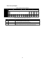
Poll Status Register
Note: These bits are only valid if IRQ=1.
Differences between the Poll Status and Poll registers:
Reading the Poll register generates a software poll. This sets the in-service bit for the
highest priority-pending interrupt.
Reading the Poll Status register does not set the in-service bit for the highest prioritypending interrupt.
Table 2-41. Poll Status Register
BIT
OFFSET
15
14
13
12
11
10
9
8
7
6
5
4
3
2
1
0
24h
FIELD
IRQ
///
RESET
RW
0
0
0
0
0
0
0
0
0
0
1
0
0
1
1
0
RW
RW
RW
RW
RW
RW
RW
RW
RW
RW
RW
RW
RW
RW
RW
RW
Table 2-42. Poll Status Register Definitions
Bits
Field Name
Description
15
IRQ
14:5
4:0
S[4:0]
Pending Interrupt
Determines whether an interrupt request is pending.
1 = interrupt request is present.
0 = interrupt request is reset (default).
Reserved
Highest Priority Interrupt Source
Contain the encoded vector type of the highest priority interrupt source.
///
Poll Register
Table 2-43. Poll Register
BIT
OFFSET
15
14
13
12
11
10
9
8
7
6
5
4
3
2
1
0
S4
S3
S2
S1
S0
0
R
W
0
R
W
0
R
W
0
R
W
0
RW
24h
FIELD
IRQ
///
RESET
RW
0
R
W
0
R
W
0
R
W
0
R
W
0
RW
0
RW
0
RW
0
RW
0
R
W
0
R
W
0
R
W
Table 2-44. Poll Register Definitions
Bits
Field Name
Description
15
IRQ
14:5
4:0
S[4:0]
Pending Interrupt
Determines whether an interrupt request is pending.
1 = interrupt request is present.
0 = interrupt request is reset (default).
Reserved
Highest Priority Interrupt Source
Contain the encoded vector type of the highest priority interrupt source.
///
29
End of Interrupt Register
Table 2-45. End of Interrupt Register
BIT
OFFSET
15
14
13
12
11
10
9
8
7
6
5
4
3
2
1
0
S4
S3
S2
S1
S0
0
R
W
0
R
W
0
R
W
0
R
W
0
RW
22h
FIELD
SPC
///
RESET
RW
0
R
W
0
R
W
0
R
W
0
R
W
0
RW
0
RW
0
RW
0
RW
0
R
W
0
R
W
0
R
W
Table 2-46. End of Interrupt Register Definitions
Bits
Field Name
Description
15
SPC
14:5
4:0
S[4:0]
Type of EOI command
1 = issue a non-specific EOI command in S4:S0.
0 = issue a specific EOI command in S4:S0 (default).
Reserved
Highest Priority Interrupt Source
Contain the encoded vector type of the highest priority interrupt source.
///
30
3: Miscellaneous Registers
Table 3-1. Miscellaneous Register Summary
Hex
Offset
AE
AC
7E
6E
6A
Mnemonic
Register Description
CAR
CDR
LEDC
PLLCLK
RNG
Checksum Adder register
Checksum Data register
LED Control register
Phase Lock Loop, Clock register
Random Number Generator register
31
Page
32
32
33
35
38
Checksum Adder Register
Always write a value to the Checksum Data register to initialize it before using the Checksum
Adder Register.
Note: The Checksum Adder register is a single hardware resource that must be protected from
being accessed simultaneously by multiple application threads.
Table 3-2. Checksum Adder Register
BIT
OFFSET
15
14
13
12
11
10
9
8
7
6
5
4
FIELD
DATA [7:0]
RESET
RW
3
2
1
0
AEh
0
R
W
0
RW
0
R
W
0
R
W
0
RW
DATA [15:8]
0
RW
0
RW
0
RW
0
R
W
0
R
W
0
R
W
0
R
W
0
R
W
0
R
W
0
R
W
0
R
W
Table 3-3. Checksum Adder Register Definitions
Bits
Field Name
Description
15:0
DATA [15:0]
Writing to this register adds the byte swapped data to the Checksum register with
carry. The data is byte-swapped during this write. This register is to be used with
TCPIP checksum generation. Reading this register shows the data in the adder.
Checksum Data Register
Table 3-4. Checksum Data Register
BIT
OFFSET
15
14
13
12
11
10
8
7
6
5
4
3
2
1
0
0
R
W
0
R
W
0
R
W
0
R
W
0
R
W
0
R
W
0
R
W
ACh
FIELD
RESET
RW
9
DATA [15:0]
0
R
W
0
RW
0
RW
0
RW
0
RW
0
RW
0
RW
0
R
W
0
R
W
Table 3-5. Checksum Data Register Definitions
Bits
Field Name
Description
15:0
DATA [15:0]
Writing to this register sets the checksum value. Typically this can be a starting value.
Reading this register shows its current value after any writes to the Checksum Adder
register.
32
LED Control Register
The LEDs normally connect to four control outputs from the internal PHY. To control the LEDs
by software, set SEN to 1.
Note: The reset value for this register, 0000h, is read as 000Dh because the LED signals
initially are driven from the PHY.
11
10
9
8
7
6
0
R
0
R
5
4
3
2
1
0
LED0
12
LED1
13
LED2
14
LED3
15
SEN
BIT
OFFSET
ENC
Table 3-6. LED Control Register
0
R
W
0
R
W
0
R
W
0
R
W
0
R
W
0
R
W
7Eh
FIELD
///
RESET
RW
0
R
0
R
0
R
0
R
0
R
0
R
0
R
0
R
Table 3-7. LED Control Register Definitions
Bits
Field Name
15:6
///
5
ENC
4
SEN
3
LED3
2
LED2
1
LED1
0
LED0
Description
Reserved
Read only as 0.
Encoding
0 = the LED signals are driven directly with no encoding.
1 = the LED signals are driven through an encoder to allow connection to two wire Bicolor LED’s. The un-encoded signals are active LOW. The encoded signals are shown
with an E in front.
0 = the LED signals are driven from the PHY.
1 = the LED signals are driven from this register.
LED3 Control Line
Normally, this bit connects to duplex signal.
If SEN = 0, the LED3 signal is driven from the PHY and reading LED3 indicates the
PHY status. When duplex is 0, the PHY is in full-duplex mode. If SEN = 1, the LED3
signal is driven from this register. See Table 3-8.
LED2 Control Line
Normally, this bit connects to the activity signal.
If SEN = 0, the LED2 signal is driven from the PHY and reading LED2 indicates the
PHY status. Activity is 0 when the PHY detects or generates valid Ethernet traffic.
If SEN = 1, the LED2 signal is driven from this register. See Table 3-8.
LED1 Control Line
Normally, this bit connects to the link signal.
If SEN = 0, the LED1 signal is driven from the PHY and reading LED1 indicates the
PHY status. Link is 0 when the PHY has a valid link.
If SEN = 1, the LED1 signal is driven from this register. See Table 3-9
LED0 Control Line
Normally, this bit connects to the 100Mbit signal.
If SEN = 0, the LED0 signal is driven from the PHY and reading LED0 indicates the
PHY status. 100Mbit is 0 when in 100Mbit mode.
If SEN = 1, the LED0 signal is driven from this register. See Table 3-9.
33
Table 3-8. LED Bits [3] and [2]
LED3
Duplex
LED2
Activity
ELED2
Green (R)
ELED3
Yellow (R)
Function
1
1
0
0
1
0
1
0
0
0
0
1
0
1
0
0
No activity
Half-duplex
No activity
Full-duplex
Table 3-9. LED Bits [1] and [0]
LED1
Link
LED0
100Mbps
ELED0
Green (L)
ELED1
Yellow (L)
Function
1
1
0
0
1
0
1
0
0
0
0
1
0
0
1
0
No link
No link
10 Mbit link
100 Mbit link
Note: The ELED signals in Table 3-8 and Table 3-9 stand for Encoded LEDs and are enabled
by ENC bit [5] in the LED Control register. The other LED signals in these tables apply when
ENC is off.
34
PLL/CLK Control Register
PLL/CLK Control is the Phase Lock Loop/Clock Control register.
Table 3-10. PLL/CLK Control Register
BIT
OFFSET
15
14
13
11
10
9
8
7
6
5
4
3
2
1
0
6Eh
//
/
///
PLL BYP N
LOCKED
FIELD
RESET
RW
12
0
RW
0
RW
⎯
R
⎯
R
Default
PLLMULT
0
R
W
0
RW
00xx
0
RW
1
1
R
RW
W
18h
USBDIV
0
R
W
0
RW
0
R
W
0
R
W
0
R
W
0
R
W
0
R
W
0
Table 3-11. PLL/CLK Control Register Definitions
Bits
Field Name
Description
15:14
13
///
PLLBYP N
12
LOCKED
11:4
PLLMULT
3:0
USBDIV
Reserved
PLL Bypass Pin
1 = PLL is being used to generate CPUCLK.
0 = PLL is being bypassed and CPUCLK is receiving a clock to use as CPUCLK.
PLL LOCKED
1 = indicates the PLL has locked onto the desired frequency set by PLLMULT.
0 = PLL is trying to change to the desired frequency. For frequencies below 13
MHz, lock may not be possible because of PLL jitter.
PLL Multiplier x1= 01h to x7Fh. Default=x18h (24 MHz)
The PLL Multiplier sets the value that the PLL uses to multiply the input clock.
With a 25 MHz crystal, the frequency will be a multiple of 1 MHz. The maximum
clock rate is limited by the CPU cycle time. Exceeding this value causes
unpredictable results. The PLL output is connected directly to the CPU Clock,
unless the PLLBYP (PLL Bypass is pulled LOW. The clock is sourced from the
CLKOUT pin, which is then tri-stated by PLLBYP_n being LOW; in this case, the
PLL is not used and should be run as slowly as possible to minimize power. Be
aware of the impact the clock frequency has on Flash access time and serial
baud rates, and adjust the other appropriate register values.
USB Clock Divider
These four bits set the USB clock divider from the PLL output clock frequency to
the USB block. The input clock to the USB divider is 2 times the CPUCLK rate
when the PLL is used (PLLBYP_n =1). The input to the USB divider is connected
to CLKOUT signal directly when PLL is disabled (PLLBYP_n = 0). See Table
3-12.
Clock Divider. /1=0000 to /16=1111. Default = /1
Note: The USB clock must be 48 MHz for USB to work properly in high-speed
mode and 6 MHz for some low-speed modes. This may limit the CPU clock
speeds that can be used if the USB is used. If the USB is not used, set the divider
to the maximum to minimize power.
35
Table 3-12. Divider Bits and Corresponding Values
6
5
0
0
0
0
0
0
0
0
0
0
0
0
0
:
:
0
:
:
0
0
:
:
0
:
:
0
1
:
:
1
:
:
1
:
:
1
:
:
1
1
1
1
1
0
0
0
0
0
0
0
0
0
0
0
0
0
:
:
0
:
:
0
1
:
:
1
:
:
1
0
:
:
0
:
:
0
:
:
1
:
:
1
1
1
1
1
PLLMULT
4 3 2 1
0
0
0
0
0
0
0
0
0
0
0
0
0
:
:
1
:
:
1
0
:
:
1
:
:
1
0
:
:
0
:
:
0
:
:
1
:
:
1
1
1
1
1
0
0
0
0
0
0
0
0
1
1
1
1
1
:
:
1
:
:
1
0
:
:
0
:
:
1
0
:
:
1
:
:
1
:
:
1
:
:
1
1
1
1
1
0
0
0
0
1
1
1
1
0
0
0
0
1
:
:
0
:
:
1
0
:
:
0
:
:
1
0
:
:
0
:
:
0
:
:
0
:
:
0
1
1
1
1
0
0
1
1
0
0
1
1
0
0
1
1
0
:
:
0
:
:
1
0
:
:
0
:
:
1
0
:
:
0
:
:
0
:
:
0
:
:
1
0
0
1
1
0
0
1
0
1
0
1
0
1
0
1
0
1
0
:
:
0
:
:
1
0
:
:
0
:
:
1
0
:
:
0
:
:
0
:
:
0
:
:
1
0
1
0
1
VCO Divider
1, 2 or 4
FB Divider
(N)
USB
Divider
4
4
4
4
4
4
4
4
4
4
4
4
4
:
:
0
1
2
3
4
5
6
7
8
9
10
11
12
:
:
-
4 (Default)
:
:
4
2
:
:
2
:
:
2
1
:
:
1
:
:
1
:
:
1
:
:
1
1
1
1
1
24(Default)
:
:
31
32
:
:
48
:
:
63
64
:
:
72
:
:
96
:
:
120
:
:
123
124
125
126
127
1
2
3
4
5
-
Clock (MHz)
USB
CPU
?
2
4
6
8
10
12
14
16
18
20
22
24
:
:
48
:
:
62
64
:
:
96
:
:
126
128
:
:
144
:
:
192
:
:
240
:
:
246
248
250
252
254
?
1
2
3
4
5
6
7
8
9
10
11
12
:
:
24
:
:
31
32
:
:
48
:
:
63
64
:
:
72
:
:
96
:
:
120
:
:
123
124
125
126
127
Notes: Gray rows show values that can be used to run the USB at standard 1 2Mbit data rates.
The internal 256K bytes of memory use different internal refresh timing. Therefore, when the
clock speed exceeds 63 MHz, fewer internal refresh cycles can be performed. This reduces the
amount of power used by the internal memory. These refresh cycles are transparent to the user
and do not effect memory access speeds. This register controls that timing. If the internal PLL is
bypassed and the CPU clock frequency exceeds 63 MHz, this register must be programmed for
64 MHz. If the internal PLL is bypassed and the CPU clock frequency is 63 MHz or less,
program this register to 24 MHz. Clock frequencies above 115 MHz are not guaranteed across
all DSTni design specifications.
36
Figure 3-1. PLL and Clock Generator
To PHY
25 Mhz to PHY
USB Divider [3:0]
25 Mhz
Crystal
PLL
To internal
PLL Status
Register
Lock
Clock
Oscillator
PLL
Pre-Divider
25Mhz
CLK
Fixed at 25
PLL &
Multiplier
10-127
1Mhz
CLK
1
PLLCLK
BYPASS
MUX
Default=24
0
Frequency Range
(20-254Mhz)
PLL Multiplier [6:0]
PLL
Post-Divider
S
Fixed at 2
PLLBYP_n
USB
Clock
Divider
1-16
CLKUSB
To internal
USB
Controller
Default=1
PLLBYP_n
CLKOUT
To External
Devices
PLLCLK/2
Frequency Range
(10-127Mhz)
Input Clock is fixed at 25Mhz.
PLLCLK is the PLL output clock and
is programmable by PLL Multiplier
(20-254Mhz). Final output frequency
after post divider is 10-127Mhz. If
PLLBYP is high then the CLKOUT is
used as an input and output to the
internal WRTCLK and USBCLK.
CLK_WRT
1.5ns before CLK_CPU
To internal CPU
and Internal
Devices
1
BYPASS
MUX
0
S
PLLBYP_n
CLK_WRT
CLK_CPU
CLOCK TREE
Clock Generator
Rev B
PLLBYP
37
Random Number Generator Register
The Random Number Generator register provides a random number for use in the TCPIP or
MAC as an address. The random-number generator is a counter running at the current CPU
clock frequency and continuously updates on each clock. The data read is a 16-bit data field.
Writes to this register are to bits [1] and [0].
Writes to this register control which type number is returned. The random numbers are not
affected by these writes. The linear version of the random number can also be used to indicate
the number of clocks that have passed for timing some code execution. The linear number
consists of two 16-bit registers, with RS=1 being the most-significant 16 bits.
Table 3-13. Random Number Generator Register
BIT
OFFSET
15
14
13
12
11
10
8
7
6
5
4
3
2
1
0
RS
LI
0
R
W
0
R
W
6Ah
FIELD
RESET
RW
9
Don’t Care
0
R
0
R
0
R
0
R
0
R
0
R
0
R
DATA[15:0]
0
0
R
R
0
R
0
R
0
R
0
R
0
R
Table 3-14. Random Number Generator Register Definitions
Bits
Field Name
15:2
1
///
RS
0
LI
15:0
DATA[15:0]
Description
Don’t Care
Register Select
0 = register 0.
1 = register 1.
Only used in Linear Number mode. See Table 3-15.
Linear
0 = selects Pseudo Random number in a 16-bit register.
1 = selects Linear numbers in a 32-register.
See Table 3-15.
Random Number Generator Data
A counter running at the current CPU clock frequency that continuously updates
on each clock.
Table 3-15. RS/LI Combinations
RS
LI
0
0
1
1
0
1
0
1
Description
Pseudo Random Number (16 bits)
Linear Clock Counter (lower 16 bits)
Reserved
Linear Clock Counter (Upper 16 bits)
38
4: Debugging In-circuit Emulator (Delce)
This chapter describes the Debugging In-circuit Emulator (Delce). Topics in this chapter include:
Theory of Operation on page 39
FS2 Target Connection on page 45
Theory of Operation
The CPU has an integrated Joint Test Action Group (JTAG) DeBugger/In-Circuit-Emulator
called CPUDICE. CPUDICE integrates an IEEE 1149.1 JTAG Test Access Port (TAP) or “slave“
controller that is typically connected to a JTAG debugger. The CPUDICE architecture has two
submodules:
BRKPTS, which contains the logic for four hardware breakpoints.
TRCEBUFF, which contains a trace buffer of 256 instructions.
Overview
Generally, users of the CPU will rely on First Silicon Solutions JTAG debugger or Paradigm
software to control the CPUDICE core. This section is provided for advanced users who want to
understand and extend the CPUDICE architecture features.
The CPUDICE architecture provides the logic to stop, single step, read/write memory,
interrogate the state of the CPU. The CPUDICE controls the CPU via JTAG instructions and the
scan chains described below.
The CPUDICE controls the CPU at the bus cycle level. This means it can force feed any byte or
word into the CPU and stop the processor between any bus cycle. The CPUDICE cannot stop
in the middle of instructions, only bus cycles (any memory or IO operation). The CPUDICE can
also insert any memory or I/O read or write into the stream while the processor is stopped or
while it is running.
The CPUDICE core provides access and control of the CPU via JTAG instructions and scan
chains.
ADDR Scan Chain
The ADDR scan chain consists of only the 24 bits of the CPUs address bus. The address bus is
setup as a separate chain to allow rapid polling of the address bus during real time operation for
generating histograms. The chain is 24 bits long with bit 0 shifted out first and bit 23 shifted out
last. The address is the linear address generated after the offset is added to the segment
register.
39
DATA Scan Chain
The DATA scan chain consists of the 16-bit DATA bus and 8 bits of control/status information.
These 24 bits are appended to the front of the ADDR scan chain. Bits [2:0] indicate the type of
cycle requested or captured as defined in the CPU STATUS signals. Bit [3] has two different
meanings, depending on whether data is being captured or cycles are being initiated.
When bus cycles are being captured, bit [3] is a one when a DMA cycle has been
captured.
When performing MEMREAD, MEMWRITE, IOREAD, or IOWRITE JTAG instructions,
program bit [3] with either a 1 when a 16-bit cycle is desired or a zero when an 8-bit
cycle is desired.
When using the APPLY_CPU instruction, bits [5] and [4] in the control chain have special
meaning. When bit [4] is set and the APPLY_CPU instruction is used, the CPU’s instruction
queue is flushed before the scanned in vector is applied. Bit [5] is a select for opcodes versus
data. When applying data for an opcode fetch, bit [5] should be clear. When applying data for a
memory or I/O read (anything but an opcode fetch), bit [5] should be set.
Table 4-1. ADDR, DATA, and STAT Scan Chain
Bits
Field Name
Description
23:0
39:24
ADDR[23:0]
DATA[15:0]
ADDR[23:0]
Data[15:0]
47:40
STAT[2:0]
STAT[2:0]
Valid settings are:
000 = interrupt ACK
001 = read IO
010 = write IO
011 = halt
100 = instruction fetch
101= read memory
110 = write memory
111 = idle
CTL[3] = sixteen
0 = 8-bit cycle
1 = 16-bit cycle
CTL[4] = IQ flush (for APPLYs)
CTL[5] = DATA (for APPLYs)
The following bits are used only in HW_BKPT chains:
CTL[4] = TR_QUAL mode
CTL[5] = OP_EXEC mode
CTL[7:6] = MODE
40
STATUS Scan Chain
The STATUS scan chain consists of a single 8-bit register with some status information as listed
in the table below.
Table 4-2. STATUS Scan Chain
Bits
Field Name
Description
7:4
3
///
Middle of Cycle
2
OP_FETCH
Reserved
Middle of Cycle
1 = only the first half of a two-part bus cycle has completed. This condition can
happen if the processor is stopped on the first bus cycle of a 16-bit access to an
odd address. Do not to insert any bus cycles when this bit is set; the processor
must first be single-stepped one bus cycle to compete the access before any bus
cycles are forced by the JTAG debugger.
OP_FETCH
1
Breakpoint Flag
0
JTAG HALT
1 = processor is expecting to fetch an opcode. This lets the debugging
software know that the processor is about to fetch an opcode. Software
can then substitute its own opcodes in place of the ones from the system
to interrogate or change the value of any register.
Breakpoint Flag
1 = the breakpoint is currently being searched. It is set when the
ENB_BKPT instruction is loaded into the instruction register.
0 = breakpoint has been found.
JTAG HALT
1 = target CPU is halted.
Hardware Breakpoints
There are four hardware BREAKPOINT scan chains. Each BREAKPOINT chain is identical to
the DATA scan chain described above except with some additional features in the CTL field and
an 8 bit COUNT field is added. The hardware breakpoint chains can be used as four individual
breakpoints, or they can be used in pairs for specifying either address ranges or in a
value/mask pair.
The control byte is as follows:
Bits [3:0] of the control byte must match for the desired cycle to trigger. If CTL[2:0]=111
then the cycle type field is ignored and a trigger will occur on any type of cycle.
The hardware breakpoints can be used in pairs for masking or to specify ranges.
HW_BKPT[1] can be paired with HW_PKPT[2] and HW_BKPT[3] can be paired with
HW_BKPT[4].
If HW_BKPT[1 or 3] is programmed with CTL[7:6]=00, the trigger condition in
HW_BKPT[1] must be met; then HW_BKPT[2] is enabled and must also be met before
the processor is halted. Only the ADDR is compared in this mode.
If HW_BKPT[1 or 3] is programmed with CTL[7:6]=01, the value on the ADDR, DATA
and STATUS busses are logically ANDed with value in HW_BKPT[2 or 4] and the result
is compared with value in HW_BKPT[1 or 3]. The CTL byte in HW_BKPT[2 or 4] is
ignored when used as a pair.
If HW_BKPT[1 or 3] is programmed with a 10, the breakpoints are used in pairs to
specify an address range as follows:
HW_BKPT[1].ADDR >= Current ADDR >= HW_BKPT[2].ADDR
41
If CTL[7:6]=11, the breakpoint is a simple address and cycle type comparison. The
cycle type can be optionally enabled with the low 3 bits of the CTL register. This mode
simply compares the current address on the bus with the value in the ADDR field of the
HW_BKPT. The DATA field is ignored. If CTL[2:0] is not equal to 11, the desired cycle
type must also match before the breakpoint triggers. Note that this mode compares the
value on the address bus and triggers on instruction queue fills.
If CTL[5]=1, the breakpoint is set to Opcode Execute Breakpoint Mode. In this mode,
the ADDR field is compared with the segment register and instruction pointer and a
breakpoint is initiated when the ADDR matches the physical address pointed to by the
segment register and instruction pointer. The comparison is NOT on the ADDR bus, but
directly on the execution units Instruction Pointer. This stops the CPU typically on the
bus cycle when the opcode is about to be executed. This mode is ideal for breaking on
specific opcodes as it will not break on the prefetch of an opcode. In this mode CTL[7:6]
are ignored.
If CTL[4]=1, the breakpoint is in Trace Qualifier mode. In this mode, the value in the
ADDR field, or the ADDR and DATA values in a register pair is used as a qualifier to
store data into the TRACE buffer.
The COUNT field counts the number of occurrences that the trigger condition must be
met before the processor is halted.
0 = disables the breakpoint.
1 = halts on the first occurrence.
0xff = halts on the 255th occurrence.
To enable a breakpoint, the desired breakpoint condition is scanned into the HW_BKPT
scan chain. Then the BREAKPT_ENB instruction should be executed and the target
processor is then allowed to run by issuing a RUN instruction. To stop the processor,
deassert control signals to the CPU after the breakpoint condition is recognized. The
breakpoint cannot stop on the actual breakpoint condition due to pipeline restrictions.
Consequently, the processor stops at an instruction boundary.
When the breakpoint is in Opcode Execute Mode, the processor stops before the
instruction is executed. In the other breakpoint modes, the processor is stopped on the
next instruction boundary after the desired bus cycle has been detected.
Trace Buffer
The TRACE scan chain is a 48-bit chain that provides access to the 256x48 bit trace buffer in
the CPUDICE core. The TRACE scan chain is also identical to the DATA scan chain. Each
word in the TRACE buffer corresponds to one bus cycle.
The TRACE buffer operates in three different modes, Normal TRACE mode, Branch history
mode, and Timer mode. In normal TRACE mode, each word in the TRACE buffer corresponds
to a single bus cycle. Trace mode can optionally use the four hardware breakpoints as qualifiers
for the data to be stored into the TRACE buffer.
In Branch History mode, the 48-bit bus is split into two 24-bit words. The low 24-bit word
corresponds to the physical address pointed to by the segment register and Instruction Pointer
value before the branch was taken (the SOURCE address). The high 24-bit word corresponds
to the CS:IP value after the branch is taken (the TARGET address). The NEWIP signal from the
CPU core is active high when the IP is about to be reloaded. The IP bus on the CPU is the
Instruction Pointer value from within the CPU execution unit. The IP bus is latched while
NEWIP is active to capture the SOURCE address. The clock after NEWIP is active the IP bus
will be latched again to capture the TARGET address.
Note: The SOURCE address always points to the last byte of the opcode. Therefore, software
must read the SOURCE address, then disassemble the code at that address and look a few
bytes backwards to find the instruction that caused the branch. If an interrupt was taken, then
TARGET address indicates that an interrupt was taken and, as a result, the SOURCE address
will point to the address of the return address after the interrupt has been serviced.
42
Timer mode also splits the 48 bit TRACE buffer into two 24 bit words. In this mode, each 24 bit
word corresponds to the number of clock cycles divided by 8 between triggers. The most
significant 2 bits indicate which trigger caused a store to the TRACE buffer. If the counter
overflows the 22-bit count range, the maximum value of all ones is stored.
The current value of the TRACE buffer pointer is available in the upper eight bits of the
TRACE_CTL scan chain. You can set the current address by scanning in a value into this
register. After a trigger has occurred, the register reflects the current pointer in the TRACE
buffer. Each time the TRACE scan chain is read, the pointer automatically increments to the
next value. Consequently, if the trace buffer size is 256, reading the TRACE scan chain 256
times reads all values in the buffer. The value scanned into the TRACE scan chain is also
written into that location of the TRACE buffer. This lets you initialize the entire buffer to make it
easier to verify that the TRACE buffer contains valid data.
Typically, the TRACE_CTL scan chain is set to 0x00 and the TRACE scan chain is read N times
(where N is the size of the trace buffer), while 48 bits of zeros are shifted in during the read.
This initializes the entire TRACE buffer with zeroes. The desired trace mode is then selected via
the TRACE_CTL and the HW_BKPT scan chains. After a trigger occurs, the TRACE buffer is
read N times. The first value read is the oldest value stored in the buffer, the second value read
is the next oldest and the last value read is the most recent value. Any values that are all zeroes
are probably unused values.
Table 4-3. TRACE Buffer
Bits
15:8
7:6
Field Name
TRACE Buffer
Address
///
5
TRACE SIZE
4
Trace Buffer Test
Mode
3:2
Mode
Description
TRACE Buffer Address
Reserved
TRACE SIZE (Read Only)
1 = 256 words.
0 = 16 words.
1:0
///
Trace Buffer Test Mode
1 = no writes to trace buffer allowed when bus cycles execute.
0 = writes to trace buffer allowed when bus cycles execute.
Mode
Mode
00 = normal
01 = branch history
10 = timer mode
11 = reserved
Reserved
43
DEICE Instructions
The Instruction register selects certain modes of operation and scan chains as described in
Table 4-4. All instructions require the least-significant two bits to be 01, which require the INST
register to be set to the appropriate settings per the 1149.1 specification.
Table 4-4. DEICE Instructions
Instruction
EXTEST
STOP
Hex
00
11
Scan Chain
RUN
ENB_BKPT
STATUS
ONE_OP
ONE_CLK
OP_ADDR
ADDR
DATA
TRACE
TRACE_CTL
BREAKPT1
BREAKPT2
BREAKPT3
BREAKPT4
MEM_WRIT
E
MEM_READ
IO_WRITE
IO_READ
APPLY
APPLY_CP
U
APPLY_EXT
21
31
41
51
61
71
81
91
A1
B1
C1
D1
E1
F1
05
ADDR
STATUS
STATUS
ADDR
ADDR
ADDR
ADDR
DATA
TRACE
TR_CTL
BREAKPT1
BREAKPT2
BREAKPT3
BREAKPT4
DATA
15
25
35
45
55
DATA
DATA
DATA
DATA
DATA
65
DATA
RESET
BYPASS
75
FF
DATA
BYPASS
ADDR
Description
Required by IEEE 1149.1
Forces READY low. CPU stops execution immediately. Remains
halted until the RUN instruction is executed.
Releases the processor from HALT.
Run until the breakpoint is reached
Select the STATUS scan chain
Execute one opcode
Execute one processor bus cycle
Capture the address of the next opcode fetch
Select the ADDR scan chain
Select the DATA scan chain
Select the TRACE scan chain
Select the TRACE Control scan chain
Select BREAKPOINT 1 scan chain
Select BREAKPOINT 2 scan chain
Select BREAKPOINT 3 scan chain
Select BREAKPOINT 4 scan chain
Initiates a MEMORY WRITE cycle
Initiates a MEMORY READ cycle
Execute an IO WRITE cycle
Execute an IO READ Cycle
Apply the scanned in vector for 1 bus cycle
Apply the scanned in vector for 1 bus cycle only to the CPU. Hold
WRN, WRLN, WRHN and RDN inactive to external logic.
Apply the scanned in vector for 1 bus cycle only to external logic.
The CPU remains inactive
Assert reset to the CPU and external peripherals
This instruction required by IEEE 1149.1. The BYPASS opcode is
automatically loaded into the INSTRUCTION register when RESET
is asserted
44
FS2 Target Connection
Figure 4-1 shows a typical connection from the CPU core to the First Silicon Solutions
Debugger.
Figure 4-1. Typical FS2 Target Connection
45
Excerpt From First Silicon Solution’s VSA186 Debugger User’s Guide
The standard target connection is the 20-position flat ribbon cable with the AMP System 50
connector. This mates to AMP connector 104549-2 (vertical surface mount), 104069-1 (rightangle through-hole), or 104068-1 (vertical through-hole) mounted on the target.
Pin
1
2
Signal
///
DBRESET
I/O
///
OUT
Active
///
HIGH
3
4
5
6
RESET
GND
///
VCC
IN
HIGH
7
8
9
10
11
12
13
14
15
16
17
18
19
20
///
GND
///
GND
///
TDI
TDO
TMS
GND
///
TCK
GND
TRST#
DBINST#
BSEN#
///
IN
///
///
///
///
///
///
///
OUT
IN
OUT
///
///
OUT
///
///
///
///
///
HIGH
HIGH
HIGH
///
///
HIGH
OUT
OUT
OUT
LOW
LOW
LOW
Comments
The target should not connect to these pins.
Driven HIGH by the debugger to reset the target system. Typically
hooked into the target power-on reset circuit.
Input to debugger informs debugger that a target reset has occurred.
Signal reference
The target should not connect to these pins.
Used by debugger to determine target power-on state. Debugger
does not draw significant current from this pin.
The target should not connect to these pins.
Signal reference
The target should not connect to these pins.
Signal reference
The target should not connect to these pins.
JTAG signal
JTAG signal
JTAG signal
Signal reference
JTAG signal
Signal reference
JTAG signal (optional)
Driven low by the debugger
Driven low by the debugger
Notes: When designing in a target system connector for the debugger, pay close attention to
the TCK signal. TCK is an edge-sensitive signal where ringing is undesirable.
DBRESET can be active HIGH or LOW. Configurable by the FS2 debugger. The RSTIN# is
active LOW. BSCEN must be HIGH for JTAG to work with the debugger.
46
5: Packaging and Electrical
This chapter describes the DSTni packaging and electrical characteristics.
Packaging
The DSTni-EX package is a 12-by-12 mm LFBGA with 0.8mm ball pitch. The part has four
thermal balls in the center to increase heat dissipation. Die size is 4.1 x 5.4 mm in 0.18u TSMC
process. Figure 5-1 describes the package.
Figure 5-1. DSTni Package
47
Recommended Circuit Board Layout
Figure 5-2. Recommended Circuit Board Layout
48
Electrical Specifications
Absolute Maximum Ratings
Table 5-1. Absolute Maximum Ratings
Parameter
Core Supply Voltage
IO Supply Voltage
Input Voltage
Output Voltage
ESD Performance
Latch-Up current
Operating Temperature
Storage Temperature
Thermal Resistance (Case)
Thermal Resistance (Ambient)
Package Dissipation
Package Dissipation
Package Dissipation
Package Dissipation
Sym
Min
VDD1.8
-0.5
VDD3.3
-0.5
Vi
-0.5
Vo
-0.5
>3K (HBM), 300 (MM), 1000 (CDM)
Ilatch
>500
TOPT
-40
TSTG
-65
(θJC)
(θJA)
105Deg C Ta
95 Deg C Ta
85 Deg C Ta
70 Deg C Ta
Max
2.5
4.6
6
6
125
150
7.6
30
0.67
1
1.33
1.83
Units
V
V
V
V
V
mA
o
C
o
C
o
C/W
o
C/W
W
W
W
W
Note: Long-term exposure to absolute maximum ratings may affect device reliability, and
permanent damage may occur if operation exceeds the rating. The device should be operated
under recommended operating conditions.
49
Recommended Operating Conditions
Table 5-2. Recommended Operating Conditions
Parameter
Core Supply Voltage (10%)
IO Supply Voltage (10%)
TJ Junction Temperature
VIL Input Low Voltage
VIH Input High Voltage
VT Threshold Point (non-Schmitt Input)
VT+ Schmitt trig low to high threshold point
VT- Schmitt trig high to low threshold point
II Input leakage current @Vi-3.3V or 0V
IOZ Tri-state output leakage current @Vo-3.3V
IOZ Tri-state output leakage current @Vo-0V
RPU Pull-up Resistor
RPD Pull-down Resistor
Ball Input Capacitance
VOL Output low voltage @IOL max
VOH Output high voltage @IOH max
IOL Low level output current @VOL 0.4V 2mA
IOL Low level output current @VOL 0.4V 4mA
IOL Low level output current @VOL 0.4V 8mA
IOL Low level output current @VOL 0.4V 12mA
IOL Low level output current @VOL 0.4V 16mA
IOL Low level output current @VOL 0.4V 24mA
IOH High level output current @VOH 2.4V 2mA
IOH High level output current @VOH 2.4V 4mA
IOH High level output current @VOH 2.4V 8mA
IOH High level output current @VOH 2.4V 12mA
IOH High level output current @VOH 2.4V 16mA
IOH High level output current @VOH 2.4V 24mA
Input Rise and fall time (10% <>90%)
CPUCLK (0 wait internal RAM)
CPUCLK (1 wait internal RAM)
VDD1.8 Current (1Mhz)
VDD1.8 Current (127Mhz)
VDD3.3 Current
PLL Jitter p/p over 200 cycles
PLL Lock Time
Min
1.62
3.0
-40
-0.3
2.0
1.46
1.50 wc
0.88 wc
///
///
///
56K
51K
///
///
2.4
2.2
4.4
8.8
13.2
17.6
24.2
-3.2
-6.4
-12.8
-19.1
-28.7
-38.2
///
1
1
///
///
///
///
20
Typ
1.8
3.3
25
///
///
1.60
1.55
0.95
±10na
10na
-10na
77K
69K
4
///
///
3.5
7.1
14.1
21.2
28.2
38.8
-6.4
-12.8
-25.7
-38.5
-57.7
-76.9
///
///
///
15
150
150
48
///
Max
1.98
3.6
125
0.8
5.5
1.76
1.55 bc
0.98 bc
±1ua
1ua
-1ua
122K
127K
///
0.4
///
4.3
8.5
17.0
25.5
34.0
46.7
-10.0
-20.0
-40.0
-60.0
-90.0
-119.9
8
100
115
20
200
200
200
150
Unit
V
V
o
C
V
V
V
V
V
///
///
///
Ω
Ω
pf
V
V
mA
mA
mA
mA
mA
mA
mA
mA
mA
mA
mA
mA
ns
Mhz
Mhz
mA
mA
mA
ps
us
Typical values are at 25oC and are for design information only and are not guaranteed and not
production tested.
Note: DSTni-EX uses two power supply voltages, one for core logic (1.8V) and another for I/O
(3.3V). If the 3.3V supply is powered and the 1.8V core logic is not powered, current in excess
of 350ma will flow into the chip. This is not a problem for short periods not to exceed 1 minute.
Longer periods could overheat DSTni and cause device failure.
50
I/O Characteristics − Xin/Xout Pins
Table 5-3. I/O Characteristics Xin/Xout Pins
Parameter
Input Clock Frequency Tolerance
Input Clock Duty Cycle
Input Capacitance
Sym
∆f
TDC
CIN
Min
///
35
///
Typ
Max
±100
65
///
///
///
3.0
Units
ppm
%
pF
PHY Receiver Input Characteristics
Table 5-4. PHY Receiver Input Characteristics
Item
Full Scale Input voltage
Input Common Mode
Spec
3.0 Differential pk-to-pk
1.6-2.0
Units
V
V
Comments
Gain dependent.
100Base-TX Transceiver Characteristics
Table 5-5. 100Base-TX Transceiver Characteristics
Parameter
Peak Differential Output Voltage
100M TX mid-level
Signal Amplitude Symmetry
Signal Rise/Fall Time
Rise/Fall Time Symmetry
Duty Cycle Distortion
Overshoot/Undershoot
Jitter (measured differentially)
Sym
VP
///
VSS
TRF
TRFS
DCD
VOS
///
Min
0.95
-50
98
3.0
///
35
///
///
Typ
///
///
///
///
///
50
///
///
Max
1.05
50
102
5.0
0.5
65
5
1.4
Units
V
mV
%
ns
ns
%
%
ns
100Base-FX Transceiver Characteristics
Table 5-6. 100Base-FX Transceiver Characteristics
Parameter
Sym
Peak Differential Output Voltage
Signal Rise/Fall Time (2pF load)
Jitter (measured differentially)
VP
TRF
///
Peak Differential Input Voltage
Common Mode Input Range
VIP
VCMIR
Min
Typ
Max
Unit
Test
Conditions
///
///
///
1.5
1.9
1.3
V
ns
ns
///
10<->90%
///
///
///
1.5
VDD-0.7
V
V
Transmitter
0.6
///
///
Receiver
0.55
///
51
///
///
100Base-T Transceiver Characteristics
Table 5-7. 100Base-T Transceiver Characteristics
Parameter
Sym
Min
Typ
Max
Unit
Test Conditions
With Transformer, line replaced
by 100Ω resistor
After line model specified by
IEEE 802.3 for 10BASE-T MAU
Transmitter
Peak Differential Output
Voltage
Transition Timing Jitter
added by the MAU and
PLS sections
VOP
Receive Input Voltage
Differential Squelch
Threshold
ZIN
VDS
///
2.2
2.5
2.8
V
0
2
11
ns
///
300
3.6
420
Receiver
///
585
///
///
kΩ
mV
100Base-T Link Integrity Timing Characteristics
Table 5-8. 100Base-T Link Integrity Timing Characteristics
Parameter
Time Link Loss Receive
Link Pulse
Link Min Receive Timer
Link Max Receive Timer
Link Transmit Period
Link Pulse Width
Sym
TLL
TLP
TLR Min
TLR Max
TLT
TLPW
Min
50
2
2
50
8
60
Typ
///
///
///
///
///
///
Max
150
7
7
150
24
150
52
Units
ms
Link Pulses
ms
ms
ms
ms
Test Conditions
///
///
///
///
///
///
Power Curve Diagrams
Figure 5-3 shows the current for both power supplies of a typical part.
Figure 5-3. DSTni Current
DSTni-EX Current
160
Current (ma)/ Temp C
140
120
1.8V Current (ma)
Temp (case) C
Ambient C
Differential C
3.3V Current (ma)
100
80
60
40
20
0
0
50
100
Frequency (Mhz)
53
150
Figure 5-4 shows shows the power dissipation of a worse-case device at four different ambient
temperatures.
Figure 5-4. DSTni Power Curve
DSTni_EX Power
1.8
Watts
1.6
1.4
Usable Pwr 12mm
115Mhz
1.2
100Mhz
72Mhz
1
50Mhz
24Mhz
10Mhz
0.8
0.6
0.4
0.2
0
105
95
85
Temperature
54
70
6: Applications
This appendix identifies various DSTni applications. Topics in this chapter include:
Timing ⎯ see page 56
Data ⎯ see page 57
Reset ⎯ see page 58
XTAL ⎯ see page 59
Burst Flash (3 wire) ⎯ see page 60
Burst Flash (2 Wire) ⎯ see page 61
Page Flash ⎯ see page 62
Serial Flash ⎯ see page 63
Static RAM ⎯ see page 64
SDRAM ⎯ see page 65
External DMA ⎯ see page 66
ARDY ⎯ see page 67
PHY (10/100 Mbit) ⎯ see page 68
Fibre (100 Mbit) ⎯ see page 69
LED Functionality ⎯ see page 70
55
Timing
56
Data
Note: For non tri-state I/O cells, the propagation delay is measured from the 50% point of the
input waveform to the 50% point of the output waveform. For tri-state I/O cells, since the tri-state
status may not exhibit any change in the output waveform, we define the propagation delay
(disable time) as the time form 50% of the disable signal to the turning on/off threshold level of
the n and p MOS transistors.
57
Reset
Power On Reset with no external connections is ~200ms. RSTOUTn is synchronized with the
internal CLKOUT before it goes inactive. External components (Cdelay and Rdelay) can extend
RSTOUTn if needed. The RSTINn input is LVTTL and TTL compatible.
58
XTAL
Power On Oscillator Startup time is 50us maximum. DSTni requires this crystal to be 25 MHz to
use either the internal PLL or Ethernet PHY. If using an external CPUCLK input (PLLBYP=0),
this crystal still is required at 25 MHz to use the Ethernet PHY. If an external oscillator is used, it
is connected to the X1 input and X2 is left open. CLKOUT cannot be used to drive X1. The
capacitors Cx1 and Cx2 include PCB capacitance.
59
Burst Flash (3 wire)
60
Burst Flash (2 Wire)
61
Page Flash
62
Serial Flash
63
Static RAM
64
SDRAM
65
External DMA
Note: WRn is not used as an input for the external DMA interface. Wait states for the internal
memory are not used for external DMA. The RDn and WRxn signals are leading-edge level
sensitive. Memory reads and writes always complete internally in one clock cycle following the
leading-edge detection. Therefore, the address bus is ignored after the rising edge of CPUCLK
after the first leading edge of RDn and WRxn. The external DMA can hold the RDn signal LOW
as long as needed for data to be read properly. The RDn can be released asynchronous to the
CPUCLK. For reads, the data is latched from the memory after one clock and continues to be
driven out the DATA BUS until released by RDn going HIGH. The external DMA can hold the
WRxn signal as long as necessary. However, the data is only written on the first rising edge of
CPUCLK after the WRxn goes LOW.
66
ARDY
Note: ARDY is internally synchronized on the falling edge of the CPUCLK. For a normally ready
system and an access cycle set for 0, wait the peripheral cannot respond in time to cause the
CPU to wait. If the system is normally not ready, this can be accomplished with difficulty. By
adding 1 wait to the access cycle, the system can respond in time to cause the CPU to wait.
However, less than ½ clock time is needed and can be difficult to generate on faster systems.
By adding 2 waits, the system can easily respond in time to cause the CPU to wait in all
systems.
67
PHY (10/100 Mbit)
The following figure shows two different, but equivalent, ways to attach DSTni to an RJ-45
connection.
68
Fibre (100 Mbit)
Note: If Fiber is not used, leave all pins open.
69
LED Functionality
This section shows the LEDs associated with DSTni and describes their functions.
Figure 6-1. LEDs
1
2
Solid: 100Base-T link
Blinking: full-duplex
Tx/Rx activity
3
Blinking: Error Indication
5
4
Solid: 100Base-T link
Blinking: full-duplex
Tx/Rx activity
6
Blinking: Power Indication
1. Blinks when transmitting or receiving packets with full-duplex LAN connection.
2. Solid when the link is established with a 100Base-T connection.
3. Blinks to indicate error detection. A pause equal to two blinking intervals is required
between the x times. If the link is good, the LED color for the pause interval is yellow or
green, depending on the 10 or 100M link. If the link is not good, the LED is OFF during the
pause interval.
Blinks 1 time = hardware error.
Blinks 2 times = duplicated IP address on the network.
Blinks 3 times = faulty network connection.
Blinks 4 times = no DHCP response received.
4. Blinks when transmitting or receiving packets with half-duplex LAN connection.
5. Solid when the link is established with a 10Base-T connection.
6. Blinks when powered on. When a 10Base-T link is detected, the LED changes to solid
green.
70
7: Instruction Clocks
Mnemonic
Opcode
Description
186
486
DSTni
AAA
AAD
AAM
AAS
ADC
AL,imm8
ADC
AX,imm16
ADC
r/m8,imm8
ADC
r/m16,imm16
ADC
r/m16,imm8
ADC
r/m8,r8
ADC
r/m16,r16
ADC
r8,r/m8
ADC
r16,r/m16
ADD
AL,imm8
ADD
AX,imm16
ADD
r/m8,imm8
ADD
r/m16,imm16
ADD
r/m16,imm8
ADD
r/m8,r8
ADD
r/m16,r16
ADD
r8,r/m8
ADD
r16,r/m16
AND
AL,imm8
AND
AX,imm16
AND
r/m8,imm8
AND
r/m16,imm16
AND
37
D5 0A
D4 0A
3F
14 ib
8
15
19
7
3
3
14
15
3
1
4
5
5
4
1
4
1
1
4/16
1/3
1/4
4/16
1/3
1/4
4/16
1/3
1/4
3/10
1/1
1/4
3/10
1/1
1/4
3/10
½
1/4
3/10
½
1/4
04 ib
ASCII-adjust AL after addition
ASCII-adjust AX before division
ASCII-adjust AL after multiplication
ASCII-adjust AL after subtraction
Add immediate byte to AL with
carry
Add immediate word to AX with
carry
Add immediate byte to r/m byte
with carry
Add immediate word to r/m byte
with carry
Add sign-extended immediate byte
to r/m word with carry
Add byte register to r/m byte with
carry
Add word register to r/m word with
carry
Add r/m byte to byte register with
carry
Add r/m word to word register with
carry
Add immediate byte to AL
3
1
1
05 iw
Add immediate word to AX
4
1
1
80 /0 ib
Add immediate byte to r/m byte
4/16
1/3
1/4
81 /0 iw
Add immediate word to r/m word
4/16
1/3
1/4
83 /0 ib
4/16
1/3
1/4
00 /r
Add sign-extended immediate byte
to r/m word
Add byte register to r/m byte
3/10
1/1
1/4
01 /r
Add word register to r/m word
3/10
1/1
1/4
02 /r
Add r/m byte to byte register
3/10
½
1/4
03 /r
Add r/m word to word register
3/10
½
1/4
24 ib
AND immediate byte with AL
3
1
1
25 iw
AND immediate word with AX
4
1
1
80 /4 ib
AND immediate byte with r/m byte
4/16
1/3
1/4
81 /4 iw
AND immediate word with r/m word
4/16
1/3
1/4
83 /4 ib
AND sign-extended immediate byte
4/16
1/3
1/4
15 iw
80 /2 ib
81 /2 iw
83 /2 ib
10 /r
11 /r
12 /r
13 /r
71
Mnemonic
r/m16,imm8
AND
r/m8,r8
AND
r/m16,r16
AND
r8,m8
AND
r16,r/m16
BOUND
r16,m16&16
CALL
rel16
CALL
r/m16
CALL
ptr16:16
CALL
m16:16
CBW
CLC
CLD
Opcode
Description
186
486
DSTni
20 /r
with r/m word
AND byte register with r/m byte
3/10
1/1
1/4
21 /r
AND word register with r/m word
3/10
1/1
1/4
22 /r
AND r/m byte with byte register
3/10
½
1/4
23 /r
AND r/m word with word register
3/10
½
1/4
62 /r
33-35
7,50
24
15
3
8
13/19
5/5
9A cd
Check to see if word register is
within bounds
Call near, displacement relative to
next instruction
Call near, register indirect/memory
indirect
Call far to full address given
23
18
FF /3
Call far to address at m16:16 word
38
17
98
F8
FC
2
2
2
3
2
2
3+J
(8)
6+J
(11)
7+J
(12)
1
1
1
2
2
3
5
2
1
1
1
1
E8 cw
FF /2
CLI
CMC
CMP
AL,imm8
CMP
AX,imm16
CMP
r/m8,imm8
CMP
r/m16,imm16
CMP
r/m16,imm8
CMP
r/m8,r8
CMP
r/m16,r16
CMP
r8,r/m8
CMP
r16,r/m16
CMPS
m8,m8
CMPS
m16,m16
CMPSB
FA
F5
3C ib
Put signed extension of AL in AX
Clear Carry Flag
Clear Direction Flag so the Source
Index (SI) and/or the Destination
Index (DI) registers will increment
during instructions
Clear Interrupt Enable Flag
Complement Carry Flag
Compare immediate byte to AL
3D iw
Compare immediate word to AX
4
1
1
80 /7 ib
3/10
½
1/4
3/10
½
1/4
3/10
½
1/4
38 /r
Compare immediate byte to r/m
byte
Compare immediate word to r/m
word
Compare sign-extended immediate
byte to r/m word
Compare byte register to r/m byte
3/10
½
1/4
39 /r
Compare word register to r/m word
3/10
½
1/4
3A /r
Compare r/m byte to byte register
3/10
½
1/4
3B /r
Compare r/m word to word register
3/10
½
1/4
A6
22
8
5
22
8
5
22
8
5
CMPSW
A7
22
8
5
CWD
99
4
3
1
DAA
DAS
DEC
27
2F
FE /1
Compare byte ES:[DI] to byte
segment:[SI]
Compare word ES:[DI] to word
segment:[SI]
Compare byte ES:[DI] to byte
DS:[SI]
Compare word ES:[DI] to word
DS:[SI]
Put signed extension of AX in
DX::AX
Decimal-adjust AL after addition
Decimal-adjust AL after subtraction
Subtract 1 from r/m byte
4
4
3/15
2
2
1/3
2
2
1/4
81 /7 iw
83 /7 ib
A7
A6
72
Mnemonic
r/m8
DEC
r/m16
DEC
r16
DIV
r/m8
DIV
r/m16
ENTER
imm16,imm8
ENTER
imm16,0
ENTER
imm16,1
ESC m
HLT
IDIV
r/m8
IDIV
r/m16
IMUL
r/m8
IMUL
r/m16
IMUL
r16,r/m16,imm
8
IMUL
r16,r/m16,imm
16
IN
AL,imm8
IN
AX,imm8
IN
AL,DX
IN
AX,DX
INC
r/m8
INC
r/m16
INC
r16
INS
m8,DX
INS
m16,DX
INSB
Opcode
Description
186
486
DSTni
FF /1
Subtract 1 from r/m word
3/15
1/3
1/4
48 + rw
Subtract 1 from word register
3
1
1
F6 /6
AL=AX/(r/m byte); AH=remainder
29/35
16/16
13/16+I
F7 /6
AX=DX::AX/(r/m word);
DX=remainder
Create stack frame for nested
procedure
Create stack frame for non-nested
procedure
Create stack frame for nested
procedure
Takes trap 7
Takes trap 7
Takes trap 7
Takes trap 7
Takes trap 7
Takes trap 7
Takes trap 7
Takes trap 7
Suspend instruction execution
AL=AX/(r/m byte); AH=remainder
38/44
24/24
21/24+I
22+
16(n-1)
15
14
14
9+
6(n-1)
7
25
17
9+6(n-1)
?
?
?
?
?
?
?
?
2
44-52/
50-58
53-61/
59-67
25-28/
31-34
34-37/
40-43
22-25
?
?
?
?
?
?
?
?
4
19/20
2+I
2+I
2+I
2+I
2+I
2+I
2+I
2+I
1
15/18+I
27/28
23/26+I
5/5
12/15
5/6
20/23
5/5
20/23
C8 iw ib
C8 iw 00
C8 iw 01
D8 /0
D9 /1
DA /2
DB /3
DC /4
DD /5
DE /6
DF /7
F4
F6 /7
F7 /7
F6 /5
AX=DX::AX/(r/m word);
DX=remainder
AX=(r/m byte)*AL
F7 /5
DX::AX=(r/m word) *AX
6B /r ib
(word register)=(r/m word)*(signextended byte integer)
69 /r iw
(word register)=(r/m word)*(signextended word integer)
29-32
5/6
20/23
E4 ib
10
17
6
10
17
6
EC
Input byte from immediate port to
AL
Input word from immediate port to
AX
Input byte from port in DX to AL
8
17
4
ED
Input word from port in DX to AX
8
17
4
FE /0
Increment r/m byte by 1
3/15
1/3
1/4
FF /0
Increment r/m word by 1
3/15
1/3
1/4
40 + rw
Increment word register by 1
3
1
1
6C
Input byte from port in DX to
ES:[DI]
Input word from port in DX to
ES:[DI]
Input byte from port in DX to
ES:[DI]
14
15
3
14
15
3
14
15
3
E5 ib
6D
6C
73
Mnemonic
Opcode
Description
186
486
DSTni
INSW
6D
14
15
3
INT 3
CC
45
26
2+I
INT
imm8
INTO
CD ib
47
30
2+I
CE
48,4
28/3
2+I
IRET
CF
28
15
7
JA rel8
JAE rel8
JB rel8
JBE rel8
JC rel8
JCXZ rel8
JE rel8
JG rel8
JGE rel8
JL rel8
JLE rel8
JMP
rel8
JMP
rel16
JMP
r/m16
JMP
ptr16:16
JMP
m16:16
JNA rel8
JNAE rel8
JNB rel8
JNBE rel8
JNC rel8
JNE rel8
JNG rel8
JNGE rel8
JNL rel8
JNLE rel8
JNO rel8
JNP rel8
JNS rel8
JNZ rel8
JO rel8
JP rel8
JPE rel8
JPO rel8
JS rel8
JZ rel8
LAHF
77 cb
73 cb
72 cb
76 cb
72 cb
E3 cb
74 cb
7F cb
7D cb
7C cb
7E cb
EB cb
Input word from port in DX to
ES:[DI]
Generate interrupt 3 (trap to
debugger)
Generate type of interrupt specified
by immediate byte
Generate interrupt 4 if Overflow
Flag (OF) is 1
Return from interrupt handler to
interrupted procedure
Jump short if above
Jump short if above or equal
Jump short if below
Jump short if above or equal
Jump short if carry
Jump short if above
Jump short if equal
Jump short if greater
Jump short if greater or equal
Jump short if less
Jump short if less or equal
Jump short direct, displacement
relative to next instruction
Jump near direct, displacement
relative to next instruction
Jump near indirect, displacement
relative to next instruction
Jump far direct to doubleword
immediate address
Jump m16:16 indirect and far
13,4
13,4
13,4
13,4
13,4
15,5
13,4
13,4
13,4
13,4
13,4
14
3/1
3/1
3/1
3/1
3/1
8/5
3/1
3/1
3/1
3/1
3/1
3
2+J
2+J
2+J
2+J
3+J
2+J
2+J
2+J
2+J
2+J
2+J
2+J
14
3
2+J
11/17
5
2+J
14
17
2+J
26
13
2+J
Jump short if not above
Jump short if not above or equal
Jump short if not below
Jump short if not below or equal
Jump short if not carry
Jump short if not equal
Jump short if not greater
Jump short if not greater or equal
Jump short if not less
Jump short if not less or equal
Jump short if not overflow
Jump short if not parity
Jump short if not sign
Jump short if not zero
Jump short if overflow
Jump short if parity
Jump short if parity even
Jump short if parity odd
Jump short if sign
Jump short if zero
Load AH with low byte of Processor
Status Flags register
Load DS:r16 with segment:offset
from memory
Load offset for m16 word in 16-bit
register
Destroy procedure stack frame
13,4
13,4
13,4
13,4
13,4
13,4
13,4
13,4
13,4
13,4
13,4
13,4
13,4
13,4
13,4
13,4
13,4
13,4
13,4
13,4
2
3/1
3/1
3/1
3/1
3/1
3/1
3/1
3/1
3/1
3/1
3/1
3/1
3/1
3/1
3/1
3/1
3/1
3/1
3/1
3/1
3
2+J
2+J
2+J
2+J
2+J
2+J
2+J
2+J
2+J
2+J
2+J
2+J
2+J
2+J
2+J
2+J
2+J
2+J
2+J
2+J
1
18
6/12
8
6
1/2
2
8
5
5
LDS
r16,m16:16
LEA
r16,m16
LEAVE
E9 cw
FF /4
EA cd
FF /5
76 cb
72 cb
73 cb
77 cb
73 cb
75 cb
7E cb
7C cb
7D cb
7F cb
71 cb
7B cb
79 cb
75 cb
70 cb
7A cb
7A cb
7B cb
78 cb
74 cb
9F
C5 /r
8D /r
C9
74
Mnemonic
Opcode
Description
186
486
DSTni
LES
C4 /r
18
6/12
8
LOCK
F0
1
1
0
LODS m8
LODS m16
LODSB
LODSW
LOOP rel8
AC
AD
AC
AD
E2
12
12
12
12
16,6
5
5
5
5
7/6
4
4
4
4
3+J
LOOPE rel8
E1 cb
16,6
9/6
3+J
LOOPNE
E0 cb
16,6
9/6
3+J
LOOPNZ
E0 cb
16,6
9/6
3+J
LOOPZ
E1 cb
16,6
9/6
3+J
MOV
r/m8,r8
MOV
r/m16,r16
MOV
r8,r/m8
MOV
r16,r/m16
MOV
r/m16,sreg
MOV
sreg,r/m16
MOV
AL,moffs8
MOV
AX,moffs16
MOV
moffs8,AL
MOV
moffs16,AX
MOV
r8,imm8
MOV
r16,imm16
MOV
r/m8,imm8
MOV
r/m16,imm16
MOVS
m8,m8
MOVS
m16,m16
MOVSB
MOVSW
MUL
r/m8
MUL
r/m16
NEG
r/m8
88 /r
Load ES:r16 with segment:offset
from memory
Asserts LOCK during an instruction
execution
Load byte segment:[SI] in AL
Load word segment:[SI] in AX
Load byte segment:[SI] in AL
Load word segment:[SI] in AX
Decrement count; jump short if CX
/=0
Decrement count; jump short if CX
/=0 and ZF=1
Decrement count; jump short if CX
/=0 and ZF=0
Decrement count; jump short if CX
/=0 and ZF=0
Decrement count; jump short if CX
/=0 and ZF=1
Copy register to r/m byte
2
1
1
89 /r
Copy register to r/m word
12
1
1
8A /r
Copy r/m byte to register
2
1
1/4
8B /r
Copy r/m word to register
9
1
1/4
8C /sr
Copy segment register to r/m word
2/11
3
1
8E /sr
Copy r/m word to segment register
2/9
3/9
1/4
A0
Copy byte at segment:offset to AL
8
1
1
A1
Copy word at segment:offset to AX
8
1
1
A2
Copy AL to byte at segment:offset
9
1
1
A3
Copy AX to word at segment:offset
9
1
1
B0+rb
Copy immediate byte to register
3
1
1
B8+rw
Copy immediate word to register
3
1
1
C6 /0
Copy immediate byte to r/m byte
12
1
1
C7 /0
Copy immediate word to r/m word
12
1
1
A4
Copy byte segment:[SI] to ES:[DI]
14
7
3
A5
Copy word segment:[SI] to ES:[DI]
14
7
3
A4
A5
F6 /4
Copy byte segment:[SI] to ES:[DI]
Copy word segment:[SI] to ES:[DI]
AX=(r/m byte)*AL
7
7
5/5
3
3
12/15
F7 /4
DX::AX=(r/m word)*AX
5/6
20/23
F6 /3
Perform a two’s complement
negation of r/m byte
14
14
26-28/
32-34
35-37/
41-43
3/10
1/3
1/4
75
Mnemonic
Opcode
Description
186
486
DSTni
NEG
r/m16
NOP
NOT
r/m8
NOT
r/m16
OR
AL,imm8
OR
AX,imm16
OR
r/m8,imm8
OR
r/m16,imm16
OR
r/m16,imm8
OR
r/m8,r8
OR
r/m16,r16
OR
r8,r/m8
OR
r16,r/m16
OUT
imm8,AL
OUT
imm8,AX
OUT
DX,AL
OUT
DX,AX
OUTS
DX,m8
OUTS
DX,m16
OUTSB
OUTSW
POP
m16
POP
r16
POP DS
POP ES
POP SS
POPA
POPF
F7 /3
3/10
1/3
1/4
90
F6 /2
Perform a two’s complement
negation of r/m word
Perform no operation
Complement each bit in r/m byte
3
3/10
1
1/3
1
1/4
F7 /2
Complement each bit in r/m word
3/10
1/3
1/4
0C ib
OR immediate byte with AL
3
1
1
0D iw
OR immediate word with AX
4
1
1
80 /1 ib
OR immediate byte with r/m byte
4/16
1/3
1/4
81 /1 iw
OR immediate word with r/m word
4/16
1/3
1/4
83 /1 ib
OR immediate byte with r/m word
4/16
1/3
1/4
08 /r
OR byte with r/m byte
3/10
1/3
1/4
09 /r
OR word with r/m word
3/10
1/3
1/4
0A /r
OR r/m byte with byte register
3/10
1/3
1/4
0B /r
OR r/m word with word register
3/10
1/3
1/4
E6 ib
Output AL to immediate port
9
19
4
E7 ib
Output AX to immediate port
9
19
4
EE
Output AL to port in DX
7
19
1
EF
Output AX to port in DX
7
19
1
6E
Output byte DS:[SI] to port in DX
14
14
4
6F
Output word DS:[SI] to port in DX
14
14
4
6E
6F
8F /0
14
14
20
14
14
5
4
4
5
10
1
5
1F
07
17
61
9D
8
8
8
51
8
4
4
4
9
9/6
5
5
5
14
5
PUSH m16
PUSH r16
PUSH imm8
FF /6
50+rw
6A
16
10
10
4
1
1
2
2
2
PUSH imm16
PUSH CS
PUSH SS
PUSH DS
PUSH ES
68
0E
16
1E
06
Output byte DS:[SI] to port in DX
Output word DS:[SI] to port in DX
Pop to word of stack into memory
word
Pop to word of stack into word
register
Pop to word of stack into DS
Pop to word of stack into ES
Pop to word of stack into SS
Pop DI, SI, BP, BX, DX, CX and AX
Pop top word of stack into
Processor Status Flags register
Push memory word onto stack
Push register word onto stack
Push sign-extended immediate
byte onto stack
Push immediate word onto stack
Push CS onto stack
Push SS onto stack
Push DS onto stack
Push ES onto stack
10
9
9
9
9
1
4
4
4
4
2
2
2
2
2
58+rw
76
Mnemonic
Opcode
Description
186
486
DSTni
PUSHA
60
36
11
14
PUSHF
9C
9
4/3
2
RCL
r/m8,1
RCL
r/m8,CL
RCL
r/m8,imm8
RCL
r/m16,1
RCL
r/m16,CL
RCL
r/m16,imm8
RCR
r/m8,1
RCR
r/m8,CL
RCR
r/m8,imm8
RCR
r/m16,1
RCR
r/m16,CL
RCR
r/m16,imm8
REP INS
m8,DX
REP INS
m16,DX
REP LODS
m8
REP LODS
m16
REP MOVS
m8,m8
REP MOVS
m16,m16
REP OUTS
DX,m8
REP OUTS
DX,m16
REP STOS
m8
REP STOS
m16
REPE CMPS
m8,m8
REPE CMPS
m16,m16
REPE SCAS
m8
REPE SCAS
m16
REPNE CMPS
m8,m8
REPNE CMPS
D0 /2
2/15
3/4
1
5+n/
17+n
5+n/
17+n
2/15
3/4
4+n
2/4
4+n
3/4
1
5+n/
17+n
5+n/
17+n
2/15
3/4
4+n
2/4
4+n
3/4
1
5+n/
17+n
5+n/
17+n
2/15
3/4
4+n
2/4
4+n
3/4
1
5+n/
17+n
5+n/
17+n
8+8n
3/4
4+n
2/4
4+n
19+11D
8+8n
19+11D
6+11n
8+8n
5/
7+4D
5/
7+4D
5/
12+3D
5/
12+3D
20+8D
8+8n
20+8D
F3 AA
Push AX, CX, DX, BX, original SP,
BP, SI and DI
Push Processor Status Flags
register
Rotate 9 bits of CF and r/m byte left
once
Rotate 9 bits of CF and r/m byte left
CL times
Rotate 9 bits of CF and r/m byte left
imm8 times
Rotate 17 bits of CF and r/m word
left once
Rotate 17 bits of CF and r/m word
left CL times
Rotate 17 bits of CF and r/m word
left imm8 times
Rotate 9 bits of CF and r/m byte
right once
Rotate 9 bits of CF and r/m byte
right CL times
Rotate 9 bits of CF and r/m byte
right imm8 times
Rotate 17 bits of CF and r/m word
right once
Rotate 17 bits of CF and r/m word
right CL times
Rotate 17 bits of CF and r/m word
right imm8 times
Input CX bytes from port in DX to
ES:[DI]
Input CX words from port in DX to
ES:[DI]
Load CX bytes from segment:[SI] in
AL
Load CX words from segment:[SI]
in AX
Copy CX bytes from segment:[SI]
in ES:[DI]
Copy CX words from segment:[SI]
in ES:[DI]
Output CX bytes from DS:[SI] to
port in DX
Output CX words from DS:[SI] to
port in DX
Fill CX bytes at ES:[DI] with AL
6+9n
F3 AB
Fill CX words at ES:[DI] with AX
6+9n
F3 A6
Find nonmatching bytes in ES:[DI]
and segment:[SI]
Find nonmatching words in ES:[DI]
and segment:[SI]
Find non-AL byte starting at ES:[DI]
5+22n
5/
7+4D
5/
7+4D
5/
7+7D
5/
7+7D
5/
7+5D
5/
7+5D
5/
7+7D
5/
4+
(D+3)n
4+
(D+3)n
4+
(D+3)n
4+
(D+3)n
4+
(D+3)n
4+
(D+3)n
4+
(D+3)n
4+
(D+3)n
4+
(D+3)n
4+
(D+3)n
4+
(D+3)n
4+
(D+3)n
4+
(D+3)n
4+
(D+3)n
4+
(D+3)n
4+
D2 /2
C0 /2 ib
D1 /2
D3 /2
C1 /2 ib
D0 /3
D2 /3
C0 /3 ib
D1 /3
D3 /3
C1 /3 ib
F3 6C
F3 6D
F3 AC
F3 AD
F3 A4
F3 A5
F3 6E
F3 6F
F3 A7
F3 AE
F3 AF
F2 A6
F2 A7
Find non-AX word starting at
ES:[DI]
Find matching bytes in ES:[DI] and
segment:[SI]
Find matching words in ES:[DI] and
77
6+11n
8+8n
8+8n
5+22n
5+15n
5+15n
5+22n
5+22n
Mnemonic
m16,m16
REPNE SCAS
m8
REPNE SCAS
m16
REPNZ CMPS
m8,m8
REPNZ CMPS
m16,m16
REPNZ SCAS
m8
REPNZ SCAS
m16
REPZ CMPS
m8,m8
REPZ CMPS
m16,m16
REPZ SCAS
m8
REPZ SCAS
m16
RET
RET
RET
imm16
RET
imm16
ROL
r/m8,1
ROL
r/m8,CL
ROL
r/m8,imm8
ROL
r/m16,1
ROL
r/m16,CL
ROL
r/m16,imm8
ROR
r/m8,1
ROR
r/m8,CL
ROR
r/m8,imm8
ROR
r/m16,1
ROR
r/m16,CL
ROR
r/m16,imm8
SAHF
SAL
r/m8,1
SAL
r/m8,CL
SAL
Opcode
Description
186
F2 AE
segment:[SI]
Find AL byte starting at ES:[DI]
5+15n
F2 AF
Find AX word starting at ES:[DI]
5+15n
F2 A6
5+22n
F2 AE
Find matching bytes in ES:[DI] and
segment:[SI]
Find matching words in ES:[DI] and
segment:[SI]
Find AL byte starting at ES:[DI]
5+15n
F2 AF
Find AX word starting at ES:[DI]
5+15n
F3 A6
Find nonmatching bytes in ES:[DI]
and segment:[SI]
Find nonmatching words in ES:[DI]
and segment:[SI]
Find non-AL byte starting at ES:[DI]
5+22n
486
DSTni
(D+3)n
4+
(D+3)n
4+
(D+3)n
4+
(D+3)n
4+
(D+3)n
4+
(D+3)n
4+
(D+3)n
4+
(D+3)n
4+
(D+3)n
4+
(D+3)n
4+
(D+3)n
3
5
7
16
22
18
CA iw
Find non-AX word starting at
ES:[DI]
Return near to calling procedure
Return far to calling procedure
Return near; pop imm16
parameters
Return far; pop imm16
7+7D
5/
7+5D
5/
7+5D
5/
7+7D
5/
7+7D
5/
7+5D
5/
7+5D
5/
7+7D
5/
7+7D
5/
7+5D
5/
7+5D
5
13
5
25
14
9
D0 /0
Rotate 8 bits of r/m byte left once
2/15
3/4
1
D2 /0
Rotate 8 bits of r/m byte left CL
times
Rotate 8 bits of r/m byte left imm8
times
Rotate 8 bits of r/m word left once
5+n/
17+n
5+n/
17+n
2/15
3/4
4+n
2/4
4+n
3/4
1
Rotate 8 bits of r/m word left CL
times
Rotate 8 bits of r/m word left imm8
times
Rotate 8 bits of r/m byte right once
5+n/
17+n
5+n/
17+n
2/15
3/4
4+n
2/4
4+n
3/4
1
Rotate 8 bits of r/m byte right CL
times
Rotate 8 bits of r/m byte right imm8
times
Rotate 8 bits of r/m word right once
5+n/
17+n
5+n/
17+n
2/15
3/4
4+n
2/4
4+n
3/4
1
5+n/
17+n
5+n/
17+n
3
3/4
4+n
2/4
4+n
2
1
D0 /4
Rotate 8 bits of r/m word right CL
times
Rotate 8 bits of r/m word right
imm8 times
Store AH in low byte of the
Processor Status Flags register
Multiply r/m byte by 2, once
2/15
3/4
1
D2 /4
Multiply r/m byte by 2, CL times
3/4
4+n
C0 /4 ib
Multiply r/m byte by 2, imm8 times
5+n/
17+n
5+n/
2/4
4+n
F2 A7
F3 A7
F3 AE
F3 AF
C3
CB
C2 iw
C0 /0 ib
D1 /0
D3 /0
C1 /0 ib
D0 /1
D2 /1
C0 /1 ib
D1 /1
D3 /1
C1 /1 ib
9E
78
5+22n
5+22n
5+15n
5+15n
Mnemonic
r/m8,imm8
SAL
r/m16,1
SAL
r/m16,CL
SAL
r/m16,imm8
SAR
r/m8,1
SAR
r/m8,CL
SAR
r/m8,imm8
SAR
r/m16,1
SAR
r/m16,CL
SAR
r/m16,imm8
SBB
AL,imm8
SBB
AX,imm16
SBB
r/m8,imm8
SBB
r/m16,imm16
SBB
r/m16,imm8
SBB
r/m8,r8
SBB
r/m16,r16
SBB
r8,r/m8
SBB
r16,r/m16
SCAS
m8
SCAS
m16
SCASB
Opcode
Description
186
486
DSTni
D1 /4
Multiply r/m word by 2, once
17+n
2/15
3/4
1
D3 /4
Multiply r/m word by 2, CL times
3/4
4+n
C1 /4 ib
Multiply r/m word by 2, imm8 times
2/4
4+n
D0 /7
5+n/
17+n
5+n/
17+n
2/15
3/4
1
5+n/
17+n
5+n/
17+n
2/15
3/4
4+n
2/4
4+n
3/4
1
5+n/
17+n
5+n/
17+n
3
3/4
4+n
2/4
4+n
1
1
4
1
1
4/16
1/3
1/4
4/16
1/3
1/4
4/16
1/3
1/4
3/10
1/3
1/4
3/10
1/3
1/4
3/10
1/3
1/4
3/10
1/3
1/4
15
6
4
15
6
4
15
6
4
15
6
4
2/15
3/4
1
5+n/
17+n
5+n/
17+n
2/15
3/4
4+n
2/4
4+n
3/4
1
5+n/
17+n
5+n/
17+n
2/15
3/4
4+n
2/4
4+n
3/4
1
SCASW
AF
SHL
r/m8,1
SHL
r/m8,CL
SHL
r/m8,imm8
SHL
r/m16,1
SHL
r/m16,CL
SHL
r/m16,imm8
SHR
r/m8,1
D0 /4
Perform a signed division of r/m
byte by 2, once
Perform a signed division of r/m
byte by 2, CL times
Perform a signed division of r/m
byte by 2, imm8 times
Perform a signed division of r/m
word by 2, once
Perform a signed division of r/m
word by 2, CL times
Perform a signed division of r/m
word by 2, imm8 times
Subtract immediate byte from AL
with borrow
Subtract immediate word from AX
with borrow
Subtract immediate byte from r/m
byte with borrow
Subtract immediate word from r/m
word with borrow
Subtract sign-extended immediate
byte from r/m word with borrow
Subtract byte register from r/m byte
with borrow
Subtract word register from r/m
word with borrow
Subtract r/m byte from byte register
with borrow
Subtract r/m word from word
register with borrow
Compare byte AL to ES:[DI];
Update DI
Compare word AX to ES:[DI];
Update DI
Compare byte AL to ES:[DI];
Update DI
Compare word AX to ES:[DI];
Update DI
Multiply r/m byte by 2, once
D2 /4
Multiply r/m byte by 2, CL times
C0 /4 ib
Multiply r/m byte by 2, imm8 times
D1 /4
Multiply r/m word by 2, once
D3 /4
Multiply r/m word by 2, CL times
C1 /4 ib
Multiply r/m word by 2, imm8 times
D0 /5
Divide unsigned r/m byte by 2,
once
D2 /7
C0 /7 ib
D1 /7
D3 /7
C1 /7 ib
1C ib
1D iw
80 /3 ib
81 /3 iw
83 /3 ib
18 /r
19 /r
1A /r
1B /r
AE
AF
AE
79
Mnemonic
Opcode
Description
186
486
DSTni
SHR
r/m8,CL
SHR
r/m8,imm8
SHR
r/m16,1
SHR
r/m16,CL
SHR
r/m16,imm8
STC
STD
D2 /5
5+n/
17+n
5+n/
17+n
2/15
3/4
4+n
2/4
4+n
3/4
1
5+n/
17+n
5+n/
17+n
2
2
3/4
4+n
2/4
4+n
2
2
1
1
STI
FB
2
5
1
STOS m8
STOS m16
AA
AB
10
10
5
5
2
2
STOSB
STOSW
AA
AB
10
10
5
5
2
2
SUB
AL,imm8
SUB
AX,imm16
SUB
r/m8,imm8
SUB
r/m16,imm16
SUB
r/m16,imm8
SUB
r/m8,r8
SUB
r/m8,r16
SUB
r8,r/m8
SUB
r16,r/m16
TEST
AL,imm8
TEST
AX,imm16
TEST
r/m8,imm8
TEST
r/m16,imm16
TEST
r/m8,r8
TEST
r/m16,r16
WAIT
XCHG
AX,r16
XCHG
r16,AX
2C ib
Divide unsigned r/m byte by 2, CL
times
Divide unsigned r/m byte by 2,
imm8 times
Divide unsigned r/m word by 2,
once
Divide unsigned r/m word by 2, CL
times
Divide unsigned r/m word by 2,
imm8 times
Set the Carry Flag to 1
Set the Direction Flag so the
Source Index (SI) and/or the
destination Index (DI) registers will
decrement during string
instructions
Enable maskable interrupts after
the next instruction
Store AL in byte ES:[DI]; Update DI
Store AX in word ES:[DI]; Update
DI
Store AL in byte ES:[DI]; Update DI
Store AX in word ES:[DI]; Update
DI
Subtract immediate byte from AL
3
1
1
2D iw
Subtract immediate word from AX
4
1
1
80 /5 ib
Subtract immediate byte from r/m
byte
Subtract immediate word from r/m
word
Subtract sign-extended immediate
byte from r/m word
Subtract byte register from r/m byte
4/16
1/3
1/4
4/16
1/3
1/4
4/16
1/3
1/4
3/10
1/3
1/4
3/10
1/3
1/4
4/16
1/3
1/4
C0 /5 ib
D1 /5
D3 /5
C1 /5 ib
F9
FD
81 /5 iw
83 /5 ib
28 /r
29 /r
2A /r
2B /r
Subtract word register from r/m
word
Subtract r/m byte from byte register
4/16
1/3
1/4
A8 ib
Subtract r/m word from word
register
AND immediate byte with AL
3
1
1
A9 iw
AND immediate word with AX
4
1
1
F6 /0 ib
AND immediate byte with r/m byte
4/10
1/2
1/4
F7 /0 iw
AND immediate word with r/m word
4/10
1/2
1/4
84 /r
AND byte register with r/m byte
3/10
1/2
1/4
85 /r
AND word register with r/m word
3/10
1/2
1/4
9B
90+rw
Performs a NOP
Exchange word register with AX
?
3
?
3
?
3
90+rw
Exchange AX with word register
3
3
3
80
Mnemonic
Opcode
Description
186
486
DSTni
XCHG
r/m8,r8
XCHG
r8,r/m8
XCHG
r/m16,r16
XCHG
r16,r/m16
XLAT
m8
XLATB
86 /r
4/17
3/5
3/7
4/17
3/5
3/7
4/17
3/5
3/7
4/17
3/5
3/7
11
4
5
11
4
5
34 ib
Exchange byte register with r/m
byte
Exchange r/m byte with byte
register
Exchange word register with r/m
word
Exchange r/m word with word
register
Set AL to memory byte
segment:[BX+unsigned AL]
Set AL to memory byte
segment:[BX+unsigned AL]
XOR immediate byte with AL
3
1
1
35 iw
XOR immediate word with AX
4
1
1
80 /6 ib
XOR immediate byte with r/m byte
4/16
1/3
1/4
81 /6 iw
XOR immediate word with r/m word
4/16
1/3
1/4
83 /6 ib
4/16
1/3
1/4
30 /r
XOR sign-extended immediate
word with r/m word
XOR byte register with r/m byte
3/10
1/3
1/4
31 /r
XOR word register with r/m word
3/10
1/3
1/4
32 /r
XOR r/m byte with byte register
3/10
1/3
1/4
33 /r
XOR r/m word with word register
3/10
1/3
1/4
86 /r
87 /r
87 /r
D7
D7
XOR
AL,imm8
XOR
AX,imm16
XOR
r/m8,imm8
XOR
r/m16,imm16
XOR
r/m16,imm8
XOR
r/m8,r8
XOR
r/m16,r16
XOR
r8,r/m8
XOR
r16,r/m16
Each instruction includes an instruction mnemonic and zero or more operands. A placeholder is
shown for operands that must be provided. The placeholder indicates the size and type of
operand that is allowed.
The Operand Is a placeholder for
imm8
An immediate byte: a signed number between –128 and 127
imm16
An immediate word: a signed number between –32768 and 32767
m
An operand in memory
m8
A byte string in memory pointed to by DS:SI or ES:DI
m16
A word string in memory pointed to by DS:SI or ES:DI
m16&16
A pair of words in memory
m16:16
A doubleword in memory that contains a signed, relative offset
displacement
moffs8
A byte in memory that contains a signed, relative offset displacement
ptr16:16
A full address (segment:offset)
r8
A general byte register: AL, BL, CL, DL, AH, BH, CH or DH
r16
A general word register: AX, BX, CX, DX, BP, SP, DI or SI
r/m8
A general byte register or a byte in memory
81
r/m16
A general word register or a word in memory
rel8
A signed, relative offset displacement between –128 and 127
rel16
A signed, relative offset displacement between –32768 and 32767
sreg
A segment register
Parameter
Indicates that
/0-/7
The Auxiliary field in the Operand Address byte specifies an extension
from 0 to 7 to the opcode instead of a register.
/r
The Auxiliary field in the Operand Address byte specifies a register
instead of an opcode extension. If the Opcode byte specifies a byte register,
the registers are assigned as follows: AL=0, CL=1, DL=2, BL=3, AH=4, CH=5,
DH=6 and BH=7. If the Opcode byte specifies a word register, the registers are
assigned as follows: AX=0, CX=1, DX=2, BX=3, SP=4, BP=5, SI=6 and DI=7.
/sr
The Auxiliary field in the Operand Address byte specifies a segment
register as follows: ES=0, CS=1, SS=2 and DS=3.
cb
The byte following the Opcode byte specifies an offset.
cd
The doubleword following the Opcode byte specifies an offset and in
some cases a segment.
cw
The word following the Opcode byte specifies an offset and in some
cases a segment
ib
The parameter is an immediate byte. The Opcode byte determines
whether it is interpreted as a signed or unsigned number.
iw
The parameter is an immediate word. The Opcode byte determines
whether it is interpreted as a signed or unsigned number.
rb
The byte register operand is specified in the Opcode byte. To determine
the Opcode byte for a particular register, add the hexadecimal value on the left
of the plus sign to the value of rb for that register as follows: AL=0, CL=1,
DL=2, BL=3, AH=4, CH=5, DH=6 and BH=7
rw
The word register operand is specified in the Opcode byte. To determine
the Opcode byte for a particular register, add the hexadecimal value on the left
of the plus sign to the value of rw for that register as follows: AX=0, CX=1,
DX=2, BX=3, SP=4, BP=5, SI=6 and DI=7.
/
This number of clocks required for a register operand is different the
number required for an operand located in memory. The number to the left
corresponds with a register operand. The number to the right corresponds with
an operand located in memory.
,
The number of clocks depends on the result of the condition tested. The
number to the left corresponds with a True or Pass result, and the number to
the right corresponds with a False or Fail result.
n
The number of clocks depends on the number of times the instruction is
repeated. n is the number of repetitions.
I
Interrupt handler +jump=18
J
Jump / queue init=5
D
Duration of instruction repeated
82
83
8: DSTni Sample Code
DstExStd.h
10-DEC-2002
This header file defines the "standard" constant
values used for all DSTni-EX module code development.
WD
Author, creation. Revision 1.00
* * * * * * * * * * * * * * * * * * * * * * * * * * * * * * * * * * * * * * *
*/
#if !defined(DSTEXSTD_H)
#define DSTEXSTD_H
#include "DstExConfig.h"
#if !defined(DST_REG_PCB)
#define DST_REG_PCB
#endif
0xFF00
/*
** * * * * * * * * * * * * * * * * * * * * * * * * * * * * * * * * * * * * * * *
** Peripheral Control Block register addresses
** Base address defined in DstLxConfig.h
** * * * * * * * * * * * * * * * * * * * * * * * * * * * * * * * * * * * * * * *
*/
/* System control and configuration registers*/
#define DST_REG_RELREG (DST_REG_PCB + 0x00FE) /* Relocation Register
*/
#define DST_REG_DCR
(DST_REG_PCB + 0x00F8) /* DSTni Configuration Reg */
#define DST_REG_RCR
(DST_REG_PCB + 0x00F6) /* Reset Configuration Reg */
#define DST_REG_PRL
(DST_REG_PCB + 0x00F4) /* Processor Release Reg
*/
#define DST_REG_AUXCON (DST_REG_PCB + 0x00F2) /* Auxiliary Configuration */
#define DST_REG_SYSCON
(DST_REG_PCB + 0x00F0) /* System Configuration
*/
/* Chip
#define
#define
#define
#define
#define
#define
#define
#define
select registers */
DST_REG_CAR
(DST_REG_PCB +
DST_REG_CDR
(DST_REG_PCB +
DST_REG_PRCS
(DST_REG_PCB +
DST_REG_MPCS
(DST_REG_PCB +
DST_REG_MMCS
(DST_REG_PCB +
DST_REG_PACS
(DST_REG_PCB +
DST_REG_LMCS
(DST_REG_PCB +
DST_REG_UMCS
(DST_REG_PCB + 0x00A0)
0x00AE) /* Checksum Adder
*/
0x00AC) /* Checksum Data
*/
0x00AA) /* Page Chip Select
*/
0x00A8) /* Memory / Peripheral Ctrl */
0x00A6) /* Mid Memory Chip Select
*/
0x00A4) /* Peripheral Chip Select
*/
0x00A2) /* Lower Memory Chip Select*/
/* Upper Memory Chip Select */
85
/* Phase lock loop, CPU clock and SPI control */
#define DST_REG_PLLCLKUSB
(DST_REG_PCB + 0x006E)
/* Watchdog timer register */
#define DST_REG_WDTCON
(DST_REG_PCB + 0x006C)
/* Random number generator / Linear counter */
#define DST_REG_RNG
(DST_REG_PCB + 0x006A)
/* SDRAM control */
#define DST_REG_SDRAMCTRL
#define DST_REG_REFMAX
/* Timer 2 registers */
#define DST_REG_T2CON
#define DST_REG_T2CMPA
(DST_REG_PCB + 0x0068) /* Control register */
(DST_REG_PCB + 0x0064) /* Refresh maxcount */
#define DST_REG_T2CNT
(DST_REG_PCB + 0x0066)
(DST_REG_PCB + 0x0062)
/*
(DST_REG_PCB + 0x0060)
/*
/*
No
/*
Control
*/
Compare A
*/
Compare B for T2 */
Count
*/
/* Timer 1 Registers */
#define DST_REG_T1CON
#define DST_REG_T1CMPB
#define DST_REG_T1CMPA
#define DST_REG_T1CNT
(DST_REG_PCB
(DST_REG_PCB
(DST_REG_PCB
(DST_REG_PCB
+
+
+
+
0x005E)
0x005C)
0x005A)
0x0058)
/*
/*
/*
/*
Control
*/
Compare B */
Compare A */
Count
*/
/* Timer 0 Registers */
#define DST_REG_T0CON
#define DST_REG_T0CMPB
#define DST_REG_T0CMPA
#define DST_REG_T0CNT
(DST_REG_PCB
(DST_REG_PCB
(DST_REG_PCB
(DST_REG_PCB
+
+
+
+
0x0056)
0x0054)
0x0052)
0x0050)
/*
/*
/*
/*
Control
*/
Compare B */
Compare A */
Count
*/
/* Interrupt controller Master Mode registers */
#define DST_REG_CANCON
(DST_REG_PCB + 0x004C) /* CAN 1 & I6 control
*/
#define DST_REG_DMA3CON
(DST_REG_PCB + 0x004A) /* DMA 3 interrupt control
#define DST_REG_DMA2CON
(DST_REG_PCB + 0x0048) /* DMA 2 interrupt control
#define DST_REG_SP3CON
(DST_REG_PCB + 0x0046) /* SP3 interrupt control
#define DST_REG_SP0CON
(DST_REG_PCB + 0x0044) /* Serial Port 0 int ctrl
#define DST_REG_SP1CON
(DST_REG_PCB + 0x0042) /* Serial Port 1 int ctrl
#define DST_REG_SP2CON
(DST_REG_PCB + 0x0040) /* Serial Port 2 int ctrl
#define DST_REG_I3CON
(DST_REG_PCB + 0x003E) /* INT3 interrupt control
#define DST_REG_USBCON
(DST_REG_PCB + 0x003E) /* USB interrupt control
#define DST_REG_SPICON
(DST_REG_PCB + 0x003C) /* SPI interrupt control
#define DST_REG_I2CCON
(DST_REG_PCB + 0x003C) /* I2C interrupt control
#define DST_REG_I1CON
(DST_REG_PCB + 0x003A) /* INT1 interrupt control
#define DST_REG_MAC1CON
(DST_REG_PCB + 0x003A) /* MAC1 interrupt control
#define DST_REG_MAC0CON
(DST_REG_PCB + 0x0038) /* MAC0 interrupt control
#define DST_REG_DMA1CON
(DST_REG_PCB + 0x0036) /* DMA 1 interrupt control
#define DST_REG_DMA0CON
(DST_REG_PCB + 0x0034) /* DMA 0 interrupt control
#define DST_REG_TCUCON
(DST_REG_PCB + 0x0032) /* Timer/Counter Unit
#define DST_REG_INTSTS
(DST_REG_PCB + 0x0030) /* Interrupt Status
#define DST_REG_REQST
(DST_REG_PCB + 0x002E) /* Interrupt Request
#define DST_REG_INSERV
(DST_REG_PCB + 0x002C) /* In-Service
#define DST_REG_PRIMSK
(DST_REG_PCB + 0x002A) /* Priority mask
#define DST_REG_IMASK
(DST_REG_PCB + 0x0028) /* Interrupt mask
#define DST_REG_POLLST
(DST_REG_PCB + 0x0026) /* Interrupt poll status
#define DST_REG_POLL
(DST_REG_PCB + 0x0024) /* Interrupt poll
#define DST_REG_EOI
(DST_REG_PCB + 0x0022) /* End Of Interrupt
/* DMA 0 control registers */
#define DST_REG_D0CON
(DST_REG_PCB + 0x00CA) /* Control */
#define DST_REG_D0TC
(DST_REG_PCB + 0x00C8) /* Terminal Count
#define DST_REG_D0DSTH
(DST_REG_PCB + 0x00C6) /* Destination hi
#define DST_REG_D0DSTL
(DST_REG_PCB + 0x00C4) /* Destination lo
#define DST_REG_D0SRCH
(DST_REG_PCB + 0x00C2) /* Source hi byte
#define DST_REG_D0SRCL
(DST_REG_PCB + 0x00C0) /* Source lo byte
86
*/
byte */
byte */
*/
*/
*/
*/
*/
*/
*/
*/
*/
*/
*/
*/
*/
*/
*/
*/
*/
*/
*/
*/
*/
*/
*/
*/
*/
*/
/* DMA 1 control registers */
#define DST_REG_D1CON
(DST_REG_PCB + 0x00DA) /* Control */
#define DST_REG_D1TC
(DST_REG_PCB + 0x00D8) /* Terminal Count
#define DST_REG_D1DSTH
(DST_REG_PCB + 0x00D6) /* Destination hi
#define DST_REG_D1DSTL
(DST_REG_PCB + 0x00D4) /* Destination lo
#define DST_REG_D1SRCH
(DST_REG_PCB + 0x00D2) /* Source hi byte
#define DST_REG_D1SRCL
(DST_REG_PCB + 0x00D0) /* Source lo byte
*/
byte */
byte */
*/
*/
/* DMA 2 control registers */
#define DST_REG_D2CON
(DST_REG_PCB + 0x009A)
#define DST_REG_D2TC
(DST_REG_PCB + 0x0098)
#define DST_REG_D2DSTH
(DST_REG_PCB + 0x0096)
#define DST_REG_D2DSTL
(DST_REG_PCB + 0x0094)
#define DST_REG_D2SRCH
(DST_REG_PCB + 0x0092)
#define DST_REG_D2SRCL
(DST_REG_PCB + 0x0090)
/*
/*
/*
/*
/*
/*
Control */
Terminal Count
Destination hi
Destination lo
Source hi byte
Source lo byte
*/
byte */
byte */
*/
*/
/* DMA 3 control registers */
#define DST_REG_D3CON
(DST_REG_PCB + 0x00BA)
#define DST_REG_D3TC
(DST_REG_PCB + 0x00B8)
#define DST_REG_D3DSTH
(DST_REG_PCB + 0x00B6)
#define DST_REG_D3DSTL
(DST_REG_PCB + 0x00B4)
#define DST_REG_D3SRCH
(DST_REG_PCB + 0x00B2)
#define DST_REG_D3SRCL
(DST_REG_PCB + 0x00B0)
/*
/*
/*
/*
/*
/*
Control */
Terminal Count
Destination hi
Destination lo
Source hi byte
Source lo byte
*/
byte */
byte */
*/
*/
/* Serial Port 3 registers */
#define DST_REG_SP3AUX
(DST_REG_PCB + 0x00EA)
#define DST_REG_SP3BAUD
(DST_REG_PCB + 0x00E8)
#define DST_REG_SP3RD
(DST_REG_PCB + 0x00E6)
#define DST_REG_SP3TD
(DST_REG_PCB + 0x00E4)
#define DST_REG_SP3STS
(DST_REG_PCB + 0x00E2)
#define DST_REG_SP3CT
(DST_REG_PCB + 0x00E0)
/*
/*
/*
/*
/*
/*
Auxiliary control */
Baud rate divisor */
Receive Data */
Transmit Data */
Status */
Control */
/* Serial Port 0 registers */
#define DST_REG_SP0AUX
(DST_REG_PCB + 0x008A)
#define DST_REG_SP0BAUD
(DST_REG_PCB + 0x0088)
#define DST_REG_SP0RD
(DST_REG_PCB + 0x0086)
#define DST_REG_SP0TD
(DST_REG_PCB + 0x0084)
#define DST_REG_SP0STS
(DST_REG_PCB + 0x0082)
#define DST_REG_SP0CT
(DST_REG_PCB + 0x0080)
/*
/*
/*
/*
/*
/*
Auxiliary control */
Baud rate divisor */
Receive Data */
Transmit Data */
Status */
Control */
/* Serial Port 1 registers */
#define DST_REG_SP1AUX
(DST_REG_PCB + 0x001A)
#define DST_REG_SP1BAUD
(DST_REG_PCB + 0x0018)
#define DST_REG_SP1RD
(DST_REG_PCB + 0x0016)
#define DST_REG_SP1TD
(DST_REG_PCB + 0x0014)
#define DST_REG_SP1STS
(DST_REG_PCB + 0x0012)
#define DST_REG_SP1CT
(DST_REG_PCB + 0x0010)
/*
/*
/*
/*
/*
/*
RS422/RS485 Control */
Baud rate divisor */
Receive Data */
Transmit Data */
Status */
Control */
/* Serial Port 2 registers */
#define DST_REG_SP2AUX
(DST_REG_PCB + 0x000A)
#define DST_REG_SP2BAUD
(DST_REG_PCB + 0x0008)
#define DST_REG_SP2RD
(DST_REG_PCB + 0x0006)
#define DST_REG_SP2TD
(DST_REG_PCB + 0x0004)
#define DST_REG_SP2STS
(DST_REG_PCB + 0x0002)
#define DST_REG_SP2CT
(DST_REG_PCB + 0x0000)
/*
/*
/*
/*
/*
/*
Auxiliary control */
Baud rate divisor */
Receive Data */
Transmit Data */
Status */
Control */
/* LED Control Register */
#define DST_REG_LEDC
(DST_REG_PCB + 0x007E)
/* Programmable I/O Bank 1 (bits 31-16) registers */
#define DST_REG_PIODATA1
(DST_REG_PCB + 0x007A)
#define DST_REG_PIODIR1
(DST_REG_PCB + 0x0078)
#define DST_REG_PIOMODE1
(DST_REG_PCB + 0x0076)
/* Input / Output Data */
/* Direction Select */
/* Mode Select */
/* Programmable I/O Bank 0 (bits 15-0) registers */
#define DST_REG_PIODATA0
(DST_REG_PCB + 0x0074)
#define DST_REG_PIODIR0
(DST_REG_PCB + 0x0072)
#define DST_REG_PIOMODE0
(DST_REG_PCB + 0x0070)
/* Input / Output Data */
/* Direction Select */
/* Mode Select */
87
/*
**
**
**
**
*/
* * * * * * * * * * * * * * * * * * * * * * * * * * * * * * * * * * * * * * *
Peripheral device I/O addresses
These are the peripheral devices not part of the Peripheral Control Block
* * * * * * * * * * * * * * * * * * * * * * * * * * * * * * * * * * * * * * *
/*
** * * * * * * * * * * * * * * * * * * * * * * * * * * * * * * * * * * * * * * *
** Ethernet Controller Registers
** * * * * * * * * * * * * * * * * * * * * * * * * * * * * * * * * * * * * * * *
*/
#define DST_ETH0_BASE
0x9000
#define DST_ETH1_BASE
0x9100
#define
#define
#define
#define
DST_REG_ETH0_RDP
DST_REG_ETH0_RAP
DST_REG_ETH0_RST
DST_REG_ETH0_MII
(DST_ETH0_BASE
(DST_ETH0_BASE
(DST_ETH0_BASE
(DST_ETH0_BASE
+
+
+
+
0x0010)
0x0012)
0x0014)
0x0018)
/*
/*
/*
/*
Register Data Port */
Register Access Port */
Reset Port */
MII Port */
#define
#define
#define
#define
DST_REG_ETH1_RDP
DST_REG_ETH1_RAP
DST_REG_ETH1_RST
DST_REG_ETH1_MII
(DST_ETH1_BASE
(DST_ETH1_BASE
(DST_ETH1_BASE
(DST_ETH1_BASE
+
+
+
+
0x0010)
0x0012)
0x0014)
0x0018)
/*
/*
/*
/*
Register Data Port */
Register Access Port */
Reset Port */
MII Port */
/*
** * * * * * * * * * * * * * * * * * * * * * * * * * * * * * * * * * * * * * * *
** CAN 0 Registers
** * * * * * * * * * * * * * * * * * * * * * * * * * * * * * * * * * * * * * * *
*/
#define DST_CAN0_BASE
0xA800
#define DST_CAN1_BASE
0xA900
/* Transmit message 0 */
#define DST_REG_CAN0_TX0_ID28_13
#define DST_REG_CAN0_TX0_ID12_00
#define DST_REG_CAN0_TX0_D63_48
#define DST_REG_CAN0_TX0_D47_32
#define DST_REG_CAN0_TX0_D31_16
#define DST_REG_CAN0_TX0_D15_00
#define DST_REG_CAN0_TX0_LEN
#define DST_REG_CAN0_TX0_CTRL
(DST_CAN0_BASE + 0x00) /*
(DST_CAN0_BASE + 0x02) /*
(DST_CAN0_BASE + 0x04)
(DST_CAN0_BASE + 0x06)
(DST_CAN0_BASE + 0x08)
(DST_CAN0_BASE + 0x0A)
(DST_CAN0_BASE + 0x0C)
(DST_CAN0_BASE + 0x0E)
Hi
Lo
/*
/*
/*
/*
/*
/*
ID bits */
ID bits */
Hi Data bits */
.... */
.... */
Lo Data bits */
Length */
Control */
/* Transmit message 1 */
#define DST_REG_CAN0_TX1_ID28_13
#define DST_REG_CAN0_TX1_ID12_00
#define DST_REG_CAN0_TX1_D63_48
#define DST_REG_CAN0_TX1_D47_32
#define DST_REG_CAN0_TX1_D31_16
#define DST_REG_CAN0_TX1_D15_00
#define DST_REG_CAN0_TX1_LEN
#define DST_REG_CAN0_TX1_CTRL
(DST_CAN0_BASE
(DST_CAN0_BASE
(DST_CAN0_BASE
(DST_CAN0_BASE
(DST_CAN0_BASE
(DST_CAN0_BASE
(DST_CAN0_BASE
(DST_CAN0_BASE
+
+
+
+
+
+
+
+
0x10)
0x12)
0x14)
0x16)
0x18)
0x1A)
0x1C)
0x1E)
/*
/*
/*
/*
/*
/*
/*
/*
Hi ID bits */
Lo ID bits */
Hi Data bits */
.... */
.... */
Lo Data bits */
Length */
Control */
/* Transmit message 2 */
#define DST_REG_CAN0_TX2_ID28_13
#define DST_REG_CAN0_TX2_ID12_00
#define DST_REG_CAN0_TX2_D63_48
#define DST_REG_CAN0_TX2_D47_32
#define DST_REG_CAN0_TX2_D31_16
#define DST_REG_CAN0_TX2_D15_00
#define DST_REG_CAN0_TX2_LEN
#define DST_REG_CAN0_TX2_CTRL
(DST_CAN0_BASE
(DST_CAN0_BASE
(DST_CAN0_BASE
(DST_CAN0_BASE
(DST_CAN0_BASE
(DST_CAN0_BASE
(DST_CAN0_BASE
(DST_CAN0_BASE
+
+
+
+
+
+
+
+
0x20)
0x22)
0x24)
0x26)
0x28)
0x2A)
0x2C)
0x2E)
/*
/*
/*
/*
/*
/*
/*
/*
Hi ID bits */
Lo ID bits */
Hi Data bits */
.... */
.... */
Lo Data bits */
Length */
Control */
88
/* Receive */
#define DST_REG_CAN0_RX_ID28_13
#define DST_REG_CAN0_RX_ID12_00
#define DST_REG_CAN0_RX_D63_48
#define DST_REG_CAN0_RX_D47_32
#define DST_REG_CAN0_RX_D31_16
#define DST_REG_CAN0_RX_D15_00
#define DST_REG_CAN0_RX_LEN
#define DST_REG_CAN0_RX_FLAGS
(DST_CAN0_BASE
(DST_CAN0_BASE
(DST_CAN0_BASE
(DST_CAN0_BASE
(DST_CAN0_BASE
(DST_CAN0_BASE
(DST_CAN0_BASE
(DST_CAN0_BASE
+
+
+
+
+
+
+
+
0x30)
0x32)
0x34)
0x36)
0x38)
0x3A)
0x3C)
0x3E)
/*
/*
/*
/*
/*
/*
/*
/*
Hi ID bit */
Lo ID bits */
Hi Data bits */
.... */
.... */
Lo Data bits */
Length */
Control */
/* Status/IRQ registers */
#define DST_REG_CAN0_ERR_CNT
#define DST_REG_CAN0_ERR_STAT_CNT
#define DST_REG_CAN0_MSG_LEVEL
#define DST_REG_CAN0_IRQ_FLAGS
#define DST_REG_CAN0_IRQ_ENABLE
(DST_CAN0_BASE
(DST_CAN0_BASE
(DST_CAN0_BASE
(DST_CAN0_BASE
(DST_CAN0_BASE
+
+
+
+
+
0x40)
0x42)
0x44)
0x46)
0x48)
/*
/*
/*
/*
/*
Rx/Tx err count */
Err Status count */
Msg Level Thresh */
Interrupt Flags */
Interrupt enable */
/* CAN Configuration */
#define DST_REG_CAN0_MODE
#define DST_REG_CAN0_BITRATE
#define DST_REG_CAN0_TIMING
(DST_CAN0_BASE + 0x4A)
(DST_CAN0_BASE + 0x4C)
(DST_CAN0_BASE + 0x4E)
/* Operating mode */
/* */
/* */
/* Acceptance Mask and Code registers */
#define DST_REG_CAN0_FILTER_ENA
(DST_CAN0_BASE + 0x50)
/* Filter enables */
#define
#define
#define
#define
#define
#define
DST_REG_CAN0_AMR0_ID28_13
DST_REG_CAN0_AMR0_ID12_00
DST_REG_CAN0_AMR0_D63_48
DST_REG_CAN0_ACR0_ID28_13
DST_REG_CAN0_ACR0_ID12_00
DST_REG_CAN0_ACR0_D63_48
(DST_CAN0_BASE
(DST_CAN0_BASE
(DST_CAN0_BASE
(DST_CAN0_BASE
(DST_CAN0_BASE
(DST_CAN0_BASE
+
+
+
+
+
+
0x52) /*Acceptance mask 0*/
0x54) /* .. */
0x56) /* .. */
0x58) /* Acceptance code 0*/
0x5A) /* .. */
0x5C) // ..
#define
#define
#define
#define
#define
#define
DST_REG_CAN0_AMR1_ID28_13
DST_REG_CAN0_AMR1_ID12_00
DST_REG_CAN0_AMR1_D63_48
DST_REG_CAN0_ACR1_ID28_13
DST_REG_CAN0_ACR1_ID12_00
DST_REG_CAN0_ACR1_D63_48
(DST_CAN0_BASE
(DST_CAN0_BASE
(DST_CAN0_BASE
(DST_CAN0_BASE
(DST_CAN0_BASE
(DST_CAN0_BASE
+
+
+
+
+
+
0x5E) /*Acceptance mask 1*/
0x60) /* .. */
0x62) /* .. */
0x64) /* Acceptance code 1*/
0x66) /* .. */
0x68) /* .. */
#define
#define
#define
#define
#define
#define
DST_REG_CAN0_AMR2_ID28_13
DST_REG_CAN0_AMR2_ID12_00
DST_REG_CAN0_AMR2_D63_48
DST_REG_CAN0_ACR2_ID28_13
DST_REG_CAN0_ACR2_ID12_00
DST_REG_CAN0_ACR2_D63_48
(DST_CAN0_BASE
(DST_CAN0_BASE
(DST_CAN0_BASE
(DST_CAN0_BASE
(DST_CAN0_BASE
(DST_CAN0_BASE
+
+
+
+
+
+
0x6A)
0x6C)
0x6E)
0x70)
0x72)
0x74)
/*Acceptance mask 2*/
/* .. */
/* .. */
/* Acceptance code 2*/
/* .. */
/* .. */
(DST_CAN0_BASE + 0x76)
(DST_CAN0_BASE + 0x78)
(DST_CAN0_BASE + 0x7A)
/* Arb. Lost Cap.Reg*/
/* Error Capture Reg*/
/* Frame Refer Reg */
/* Analysis registers */
#define DST_REG_CAN0_ALCR
#define DST_REG_CAN0_ECR
#define DST_REG_CAN0_FRR
/*
** * * * * * * * * * * * * * * * * * * * * * * * * * * * * * * * * * * * * * * *
** CAN 1 Registers
** * * * * * * * * * * * * * * * * * * * * * * * * * * * * * * * * * * * * * * *
*/
/* Transmit message 0 */
#define DST_REG_CAN1_TX0_ID28_13
#define DST_REG_CAN1_TX0_ID12_00
#define DST_REG_CAN1_TX0_D63_48
#define DST_REG_CAN1_TX0_D47_32
#define DST_REG_CAN1_TX0_D31_16
#define DST_REG_CAN1_TX0_D15_00
#define DST_REG_CAN1_TX0_LEN
#define DST_REG_CAN1_TX0_CTRL
(DST_CAN1_BASE
(DST_CAN1_BASE
(DST_CAN1_BASE
(DST_CAN1_BASE
(DST_CAN1_BASE
(DST_CAN1_BASE
(DST_CAN1_BASE
(DST_CAN1_BASE
+
+
+
+
+
+
+
+
89
0x00)
0x02)
0x04)
0x06)
0x08)
0x0A)
0x0C)
0x0E)
/*
/*
/*
/*
/*
/*
/*
/*
Hi ID bits */
Lo ID bits */
Hi Data bits */
.... */
.... */
Lo Data bits */
Length */
Control */
/* Transmit message 1 */
#define DST_REG_CAN1_TX1_ID28_13
#define DST_REG_CAN1_TX1_ID12_00
#define DST_REG_CAN1_TX1_D63_48
#define DST_REG_CAN1_TX1_D47_32
#define DST_REG_CAN1_TX1_D31_16
#define DST_REG_CAN1_TX1_D15_00
#define DST_REG_CAN1_TX1_LEN
#define DST_REG_CAN1_TX1_CTRL
(DST_CAN1_BASE
(DST_CAN1_BASE
(DST_CAN1_BASE
(DST_CAN1_BASE
(DST_CAN1_BASE
(DST_CAN1_BASE
(DST_CAN1_BASE
(DST_CAN1_BASE
+
+
+
+
+
+
+
+
0x10)
0x12)
0x14)
0x16)
0x18)
0x1A)
0x1C)
0x1E)
/*
/*
/*
/*
/*
/*
/*
/*
Hi ID bits */
Lo ID bits */
Hi Data bits */
.... */
.... */
Lo Data bits */
Length */
Control */
/* Transmit message 2 */
#define DST_REG_CAN1_TX2_ID28_13
#define DST_REG_CAN1_TX2_ID12_00
#define DST_REG_CAN1_TX2_D63_48
#define DST_REG_CAN1_TX2_D47_32
#define DST_REG_CAN1_TX2_D31_16
#define DST_REG_CAN1_TX2_D15_00
#define DST_REG_CAN1_TX2_LEN
#define DST_REG_CAN1_TX2_CTRL
(DST_CAN1_BASE
(DST_CAN1_BASE
(DST_CAN1_BASE
(DST_CAN1_BASE
(DST_CAN1_BASE
(DST_CAN1_BASE
(DST_CAN1_BASE
(DST_CAN1_BASE
+
+
+
+
+
+
+
+
0x20)
0x22)
0x24)
0x26)
0x28)
0x2A)
0x2C)
0x2E)
/*
/*
/*
/*
/*
/*
/*
/*
Hi ID bits */
Lo ID bits */
Hi Data bits */
.... */
.... */
Lo Data bits */
Length */
Control */
/* Receive */
#define DST_REG_CAN1_RX_ID28_13
#define DST_REG_CAN1_RX_ID12_00
#define DST_REG_CAN1_RX_D63_48
#define DST_REG_CAN1_RX_D47_32
#define DST_REG_CAN1_RX_D31_16
#define DST_REG_CAN1_RX_D15_00
#define DST_REG_CAN1_RX_LEN
#define DST_REG_CAN1_RX_FLAGS
(DST_CAN1_BASE
(DST_CAN1_BASE
(DST_CAN1_BASE
(DST_CAN1_BASE
(DST_CAN1_BASE
(DST_CAN1_BASE
(DST_CAN1_BASE
(DST_CAN1_BASE
+
+
+
+
+
+
+
+
0x30)
0x32)
0x34)
0x36)
0x38)
0x3A)
0x3C)
0x3E)
/*
/*
/*
/*
/*
/*
/*
/*
Hi ID bit */
Lo ID bits */
Hi Data bits */
.... */
.... */
Lo Data bits */
Length */
Control */
/* Status/IRQ registers */
#define DST_REG_CAN1_TX_ERR_CNT
#define DST_REG_CAN1_ERR_STAT_CNT
#define DST_REG_CAN1_MSG_LEVEL
#define DST_REG_CAN1_IRQ_FLAGS
#define DST_REG_CAN1_IRQ_ENABLE
(DST_CAN1_BASE
(DST_CAN1_BASE
(DST_CAN1_BASE
(DST_CAN1_BASE
(DST_CAN1_BASE
+
+
+
+
+
0x40)
0x42)
0x44)
0x46)
0x48)
/*
/*
/*
/*
/*
Rx/Tx err count
Error Stat count
Msg Level Thresh
Interrupt Flags
Interrupt enable
/* CAN Configuration */
#define DST_REG_CAN1_MODE
#define DST_REG_CAN1_BITRATE
#define DST_REG_CAN1_TIMING
(DST_CAN1_BASE + 0x4A)
(DST_CAN1_BASE + 0x4C)
(DST_CAN1_BASE + 0x4E)
/* Operating mode */
/* */
/* */
/* Acceptance mask and code registers */
#define DST_REG_CAN1_FILTER_ENA
(DST_CAN1_BASE + 0x50)
/* Filter enables */
#define
#define
#define
#define
#define
#define
DST_REG_CAN1_AMR0_ID28_13
DST_REG_CAN1_AMR0_ID12_00
DST_REG_CAN1_AMR0_D63_48
DST_REG_CAN1_ACR0_ID28_13
DST_REG_CAN1_ACR0_ID12_00
DST_REG_CAN1_ACR0_D63_48
(DST_CAN1_BASE
(DST_CAN1_BASE
(DST_CAN1_BASE
(DST_CAN1_BASE
(DST_CAN1_BASE
(DST_CAN1_BASE
+
+
+
+
+
+
0x52)
0x54)
0x56)
0x58)
0x5A)
0x5C)
/*Acceptance mask 0*/
/* .. */
/* .. */
/* Acceptance code 0*/
/* .. */
/* .. */
#define
#define
#define
#define
#define
#define
DST_REG_CAN1_AMR1_ID28_13
DST_REG_CAN1_AMR1_ID12_00
DST_REG_CAN1_AMR1_D63_48
DST_REG_CAN1_ACR1_ID28_13
DST_REG_CAN1_ACR1_ID12_00
DST_REG_CAN1_ACR1_D63_48
(DST_CAN1_BASE
(DST_CAN1_BASE
(DST_CAN1_BASE
(DST_CAN1_BASE
(DST_CAN1_BASE
(DST_CAN1_BASE
+
+
+
+
+
+
0x5E)
0x60)
0x62)
0x64)
0x66)
0x68)
/*Acceptance mask 1*/
/* .. */
/* .. */
/* Acceptance code 1*/
/* .. */
/* .. */
#define
#define
#define
#define
#define
#define
DST_REG_CAN1_AMR2_ID28_13
DST_REG_CAN1_AMR2_ID12_00
DST_REG_CAN1_AMR2_D63_48
DST_REG_CAN1_ACR2_ID28_13
DST_REG_CAN1_ACR2_ID12_00
DST_REG_CAN1_ACR2_D63_48
(DST_CAN1_BASE
(DST_CAN1_BASE
(DST_CAN1_BASE
(DST_CAN1_BASE
(DST_CAN1_BASE
(DST_CAN1_BASE
+
+
+
+
+
+
0x6A)
0x6C)
0x6E)
0x70)
0x72)
0x74)
/*Acceptance mask 2*/
/* .. */
/* .. */
/* Acceptance code 2*/
/* .. */
/* .. */
(DST_CAN1_BASE + 0x76)
(DST_CAN1_BASE + 0x78)
(DST_CAN1_BASE + 0x7A)
/* Arb. Lost Cap Reg*/
/* Error Capture Reg*/
/* Frame Ref. Reg. */
/* Analysis registers */
#define DST_REG_CAN1_ALCR
#define DST_REG_CAN1_ECR
#define DST_REG_CAN1_FRR
/*
** * * * * * * * * * * * * * * * * * * * * * * * * * * * * * * * * * * * * * * *
** Serial Peripheral Inteface registers
** * * * * * * * * * * * * * * * * * * * * * * * * * * * * * * * * * * * * * * *
*/
#define DST_SPI0_BASE
0xB800
#define DST_REG_SPICTRHI
#define DST_REG_SPICTRLO
#define DST_REG_SPISSEL
(DST_SPI0_BASE + 0x0A)
(DST_SPI0_BASE + 0x08)
(DST_SPI0_BASE + 0x06)
90
/* High byte of counter */
/* Low byte of counter */
/* Slave Select */
*/
*/
*/
*/
*/
#define DST_REG_SPISTAT
#define DST_REG_SPICTRL
#define DST_REG_SPIDATA
(DST_SPI0_BASE + 0x04)
(DST_SPI0_BASE + 0x02)
(DST_SPI0_BASE + 0x00)
/* Status */
/* Control */
/* Write / Read data */
/*
** * * * * * * * * * * * * * * * * * * * * * * * * * * * * * * * * * * * * * * *
** USB Controller Registers
** * * * * * * * * * * * * * * * * * * * * * * * * * * * * * * * * * * * * * * *
*/
#define DST_USB0_BASE
0x9800
#define
#define
#define
#define
#define
#define
#define
#define
#define
#define
#define
#define
#define
DST_REG_USB_INT_STAT
(DST_USB0_BASE + 0x00) /* Interrupt status */
DST_REG_USB_INT_ENB
(DST_USB0_BASE + 0x01) /* Interrupt enable */
DST_REG_USB_ERR_STAT
(DST_USB0_BASE + 0x02) /* Error Int. status */
DST_REG_USB_ERR_ENB
(DST_USB0_BASE + 0x03) /* Error Int. enable */
DST_REG_USB_STAT
(DST_USB0_BASE + 0x04) /* Status */
DST_REG_USB_CTL
(DST_USB0_BASE + 0x05) /* Control */
DST_REG_USB_ADDR
(DST_USB0_BASE + 0x06) /* Address */
DST_REG_USB_BDT_PAGE
(DST_USB0_BASE + 0x07) /* Buf descr table */
DST_REG_USB_FRM_NUML (DST_USB0_BASE + 0x08) /* Frame num 7:0 */
DST_REG_USB_FRM_NUMH (DST_USB0_BASE + 0x09) /* Frame num 10:8 */
DST_REG_USB_TOKEN
(DST_USB0_BASE + 0x0A) /* Token */
DST_REG_USB_SOF_THLDL (DST_USB0_BASE + 0x0B) /* SOF Thres 15:8 */
DST_REG_USB_SOF_THLDH
(DST_USB0_BASE + 0x0C) /* SOF Threshold 7:0 */
#define
#define
#define
#define
#define
#define
#define
#define
#define
#define
#define
#define
#define
#define
#define
#define
DST_REG_USB_ENDPT0
DST_REG_USB_ENDPT1
DST_REG_USB_ENDPT2
DST_REG_USB_ENDPT3
DST_REG_USB_ENDPT4
DST_REG_USB_ENDPT5
DST_REG_USB_ENDPT6
DST_REG_USB_ENDPT7
DST_REG_USB_ENDPT8
DST_REG_USB_ENDPT9
DST_REG_USB_ENDPT10
DST_REG_USB_ENDPT11
DST_REG_USB_ENDPT12
DST_REG_USB_ENDPT13
DST_REG_USB_ENDPT14
DST_REG_USB_ENDPT15
(DST_USB0_BASE
(DST_USB0_BASE
(DST_USB0_BASE
(DST_USB0_BASE
(DST_USB0_BASE
(DST_USB0_BASE
(DST_USB0_BASE
(DST_USB0_BASE
(DST_USB0_BASE
(DST_USB0_BASE
(DST_USB0_BASE
(DST_USB0_BASE
(DST_USB0_BASE
(DST_USB0_BASE
(DST_USB0_BASE
(DST_USB0_BASE
+
+
+
+
+
+
+
+
+
+
+
+
+
+
+
+
0x10)
0x11)
0x12)
0x13)
0x14)
0x15)
0x16)
0x17)
0x18)
0x19)
0x1A)
0x1B)
0x1C)
0x1D)
0x1E)
0x1F)
/*
/*
/*
/*
/*
/*
/*
/*
/*
/*
/*
/*
/*
/*
/*
/*
Endpoint
Endpoint
Endpoint
Endpoint
Endpoint
Endpoint
Endpoint
Endpoint
Endpoint
Endpoint
Endpoint
Endpoint
Endpoint
Endpoint
Endpoint
Endpoint
0 control */
1 control */
2 control */
3 control */
4 control */
5 control */
6 control */
7 control */
8 control */
9 control */
10 control */
11 control */
12 control */
13 control */
14 control */
15 control */
/*
** * * * * * * * * * * * * * * * * * * * * * * * * * * * * * * * * * * * * * * *
** I2C Controller Registers
** * * * * * * * * * * * * * * * * * * * * * * * * * * * * * * * * * * * * * * *
*/
#define DST_I2C0_BASE
0xD000
#define
#define
#define
#define
#define
#define
#define
DST_REG_I2CSRST
DST_REG_I2CXADDR
DST_REG_I2CCCR
DST_REG_I2CSTAT
DST_REG_I2CCNTR
DST_REG_I2CDATA
DST_REG_I2CADDR
(DST_I2C0_BASE
(DST_I2C0_BASE
(DST_I2C0_BASE
(DST_I2C0_BASE
(DST_I2C0_BASE
(DST_I2C0_BASE
(DST_I2C0_BASE
+
+
+
+
+
+
+
0x0E)
0x08)
0x06)
0x06)
0x04)
0x02)
0x00)
91
/*
/*
/*
/*
/*
/*
/*
Software Reset */
Extended Slave Addr */
Clock Control */
Status */
Control */
Data */
Address */
/*
** * * * * * * * * * * * * * * * * * * * * * * * * * * * * * * * * * * * * * * *
** Register field defines and masks
** * * * * * * * * * * * * * * * * * * * * * * * * * * * * * * * * * * * * * * *
*/
/* PCB/RELREG - Relocation Register */
#define DST_RELREG_PCB_IN_MEM
0x1000
/* Puts PCB in memory space */
#define DST_RELREG_PCB_IN_IO
0x0000
/* Puts PCB in I/O space */
/* PRL - Processor Revision Level */
#define DST_PRL_MSK_REV
#define DST_PRL_MSK_CPU
0xFF00
0x00FF
/* Revision Number */
/* CPU number */
/* PCB/AUXCON - Auxiliary Configuration */
#define DST_AUXCON_ENRX3
#define DST_AUXCON_DTE3
#define DST_AUXCON_ENRX2
#define DST_AUXCON_DTE2
#define DST_AUXCON_ENRX1
#define DST_AUXCON_DTE1
#define DST_AUXCON_ENRX0
#define DST_AUXCON_DTE0
0x0400
0x0200
0x0100
0x0080
0x0040
0x0020
0x0010/*
0x0008
/* Selects ENRX mode SP3 CTS/ENRX */
/* Selects RTS mode SP3 RTR/RTS */
/* Selects ENRX mode SP2 CTS/ENRX */
/* Selects RTS mode SP2 RTR/RTS pin */
/* Selects ENRX mode SP1 CTS/ENRX */
/* Selects RTS mode SP1 RTR/RTS pin */
Selects ENRX mode SP0 CTS/ENRX pin */
/* Selects RTS mode SP0 RTR/RTS pin */
/* PCB/SYSCON - System Configuration (read-only) */
#define DST_SYSCON_MCS0
0x4000 /* Enable MSC0 over entire MCS range */
#define DST_SYSCON_CD
0x0100 /* Disable clock output */
/* DCR - DSTni Configuration Register */
#define DST_DCR_BROMEN
0x4000 /* Boot ROM enabled */
#define DST_DCR_ADDR24
0x2000 /* Extended address mode enabled */
#define DST_DCR_WDOGEN
0x1000 /* Watchdog enabled */
#define DST_DCR_SPIBOOT
0x0800 /* Boot from SPI enabled */
#define DST_DCR_SPIEN
0x0400 /* SPI pins enabled in PIO */
#define DST_DCR_ETHBOOT
0x0200 /* Ethernet boot enabled */
#define DST_DCR_ETHCHAN
0x0100 /* Ethernet channel 1 selected */
#define DST_DCR_BICOLOR
0x0080 /* Using encoded LEDs */
#define DST_DCR_PARBOOT
0x0040 /* Boot from parallel flash enabled */
#define DST_DCR_PHYBYPASS
0x0020 /* Do not access Ethernet PHY via MII */
#define DST_DCR_BYTEMODE
0x0010 /* Select hi/lo byte read */
#define DST_DCR_SERBOOT
0x0008 /* Enable boot via serial port */
#define DST_DCR_SERCHAN
0x0004 /* Select serial port 0 or 1 for boot */
#define DST_DCR_SERSPEED
0x0002 /* Select 9600 baud serial speed */
#define DST_DCR_DEBUG
0x0001 /* Enable boot debug messages */
/* PCB/WDTCON - Watchdog control */
#define DST_WDTCON_ENA
#define DST_WDTCON_WRST
#define DST_WDTCON_RSTFLAG
#define DST_WDTCON_NMIFLAG
#define DST_WDTCON_UNLOCK
#define DST_WDTCON_EXP_10
#define DST_WDTCON_EXP_20
#define DST_WDTCON_EXP_21
#define DST_WDTCON_EXP_22
#define DST_WDTCON_EXP_23
#define DST_WDTCON_EXP_24
#define DST_WDTCON_EXP_25
#define DST_WDTCON_EXP_26
#define DST_WDTCON_EXP_27
#define DST_WDTCON_EXP_28
#define DST_WDTCON_EXP_29
#define DST_WDTCON_RESET_1
#define DST_WDTCON_RESET_2
#define DST_WDTCON_OPEN_1
#define DST_WDTCON_OPEN_2
0x2000
0x1000
0x0800
0xAAAA
0x5555
0x8000
/* Enable timer */
0x4000
/* Cause a reset upon timeout */
/* Set if a WD reset has happened */
/* Set if a NMI event occurred */
/* Unlock reg for further writes */
0x0001
/* Set WDT timer exponent to 10 */
0x0002
/* Set WDT timer exponent to 20 */
0x0004
/* Set WDT timer exponent to 21 */
0x0008
/* Set WDT timer exponent to 22 */
0x0010
/* Set WDT timer exponent to 23 */
0x0020
/* Set WDT timer exponent to 24 */
0x0040
/* Set WDT timer exponent to 25 */
0x0080
/* Set WDT timer exponent to 26 */
0x0100
/* Set WDT timer exponent to 27 */
0x0200
/* Set WDT timer exponent to 28 */
0x0400
/* Set WDT timer exponent to 29 */
/* First of 2 reset steps */
/* Second of 2 reset steps */
0x3333
/* First of 2 open-for-write steps */
0xCCCC
/* Second of 2 open-for-write steps */
92
/* PCB/T0CON - Timer 0 Control */
#define DST_T0CON_ENABLE
#define DST_T0CON_DISABLE
#define DST_T0CON_INT_ENABLE
#define DST_T0CON_RIU
#define DST_T0CON_MC
#define DST_T0CON_RTG
#define DST_T0CON_P
#define DST_T0CON_EXT
#define DST_T0CON_ALT
#define DST_T0CON_CONT
0xC000
/*
0x4000
/*
0x2000
/* Enable
0x1000
/*
0x0020
/*
0x0010
/*
0x0008
/*
0x0004
/*
0x0002
/*
0x0001
/*
Enables Timer */
Disables Timer */
interrupts */
0 = maxcount A in use,else maxcnt B*/
If 1, maxcount has been reached */
Use TMRIN0 to reset count */
Use Timer 2 as prescale */
Use TMRIN0 as external clock source */
Alternate between Maxcount A and B */
Run in continuous mode */
/* PCB/T1CON - Timer 1 Control */
#define DST_T1CON_ENABLE
#define DST_T1CON_DISABLE
#define DST_T1CON_INT_ENABLE
#define DST_T1CON_RIU
#define DST_T1CON_MC
#define DST_T1CON_RTG
#define DST_T1CON_P
#define DST_T1CON_EXT
#define DST_T1CON_ALT
#define DST_T1CON_CONT
0xC000
/*
0x4000
/*
0x2000
/* Enable
0x1000
/*
0x0020
/*
0x0010
/*
0x0008
/*
0x0004
/*
0x0002
/*
0x0001
/*
Enables Timer */
Disables Timer */
interrupts */
0 = maxcnt A in use, else maxcnt B*/
If 1, maxcnt has been reached */
Use TMRIN0 to reset count */
Use Timer 2 as prescale */
Use TMRIN0 as external clock source */
Alternate between Maxcnt A and B */
Run in continuous mode */
/* PCB/T2CON - Timer 2 Control */
#define DST_T2CON_ENABLE
#define DST_T2CON_DISABLE
#define DST_T2CON_INT_ENABLE
#define DST_T2CON_MC
#define DST_T2CON_CONT
0xC000
/*
0x4000
/*
0x2000
/* Enable
0x0020
/*
0x0001
/*
Enables Timer */
Disables Timer */
interrupts */
If 1, maxcount has been reached */
Run in continuous mode */
/* PCB/INSERV - Interrupt in-service */
#define DST_INSERV_CAN
#define DST_INSERV_DMA3
#define DST_INSERV_DMA2
#define DST_INSERV_SP3
#define DST_INSERV_INT5
#define DST_INSERV_SP0
#define DST_INSERV_SP1
#define DST_INSERV_SP2
#define DST_INSERV_USB
#define DST_INSERV_INT3
#define DST_INSERV_SPI
#define DST_INSERV_I2C
#define DST_INSERV_MAC1
#define DST_INSERV_INT1
#define DST_INSERV_MAC0
#define DST_INSERV_DMA1
#define DST_INSERV_DMA0
#define DST_INSERV_TMR
0x4000
0x2000
0x1000
0x0800
0x0800
0x0400
0x0200
0x0100
0x0080
0x0080
0x0040
0x0040
0x0020
0x0020
0x0010
0x0008
0x0004
0x0001
/* PCB/REQST - Interrupt request */
#define DST_REQST_DMA3
#define DST_REQST_DMA2
#define DST_REQST_SP3
#define DST_REQST_INT5
#define DST_REQST_SP0
#define DST_REQST_SP1
#define DST_REQST_SP2
#define DST_REQST_USB
#define DST_REQST_INT3
#define DST_REQST_SPI
#define DST_REQST_I2C
#define DST_REQST_INT1
#define DST_REQST_MAC1
#define DST_REQST_MAC0
#define DST_REQST_DMA1
#define DST_REQST_DMA0
#define DST_REQST_TMR
/* DMA channel 3 */
/* DMA channel 2 */
/* I5: serial port 3 */
0x0800
/* I5: Extneral INT5 pin */
/* Serial Port 0 */
/* Serial Port 1 */
/* Serial Port 2 */
/* I3: USB */
/* I3: External INT 3 pin */
/* I2: SPI */
/* I2: I2C */
/* I1: External INT1 pin */
0x0020
/* I1: Ethernet MAC1 */
/* I0: Ethernet MAC0 */
/* DMA channel 1 */
/* DMA channel 0 */
/* Timer (0, 1 or 2) */
0x2000
0x1000
0x0800
0x0400
0x0200
0x0100
0x0080
0x0080
0x0040
0x0040
0x0020
0x0010
0x0008
0x0004
0x0001
93
/*
/*
/*
/*
/*
/*
/*
/*
/*
/*
/*
/*
/*
/*
/*
/*
/*
/*
I6: CAN1 and CAN0 */
DMA channel 3 */
DMA channel 2 */
I5: serial port 3 */
I5: Extneral INT5 pin */
Serial Port 0 */
Serial Port 1 */
Serial Port 2 */
I3: USB */
I3: External INT 3 pin */
I2: SPI */
I2: I2C */
I1: Ethernet MAC1 */
I1: External INT1 pin */
I0: Ethernet MAC0 */
DMA channel 1 */
DMA channel 0 */
Timer (0, 1 or 2) */
/* PCB/IMASK - Interrupt mask */
#define DST_IMASK_DMA3
#define DST_IMASK_DMA2
#define DST_IMASK_SP3
#define DST_REQST_INT5
#define DST_IMASK_SP0
#define DST_IMASK_SP1
#define DST_IMASK_SP2
#define DST_IMASK_USB
#define DST_IMASK_INT3
#define DST_IMASK_SPI
#define DST_IMASK_I2C
#define DST_IMASK_INT1
#define DST_IMASK_MAC1
#define DST_IMASK_MAC0
#define DST_IMASK_DMA1
#define DST_IMASK_DMA0
#define DST_IMASK_TMR
#define DST_IMASK_ALL
0x2000
0x1000
0x0800
0x0400
0x0200
0x0100
0x0080
0x0080
0x0040
0x0040
0x0020
0x0010
0x0008
0x0004
0x0001
/* DMA channel 3 */
/* DMA channel 2 */
/* I5: serial port 3 */
0x0800
/* I5: Extneral INT5 pin */
/* Serial Port 0 */
/* Serial Port 1 */
/* Serial Port 2 */
/* I3: USB */
/* I3: External INT 3 pin */
/* I2: SPI */
/* I2: I2C */
/* I1: External INT1 pin */
0x0020
/* I1: Ethernet MAC1 */
/* I0: Ethernet MAC0 */
/* DMA channel 1 */
/* DMA channel 0 */
/* Timer (0, 1 or 2) */
0x7FFD
/* Mask all interrupt sources */
/* PCB/PRIMSK - Interrupt priority mask */
#define DST_PRIMSK_L7
#define DST_PRIMSK_L6
#define DST_PRIMSK_L5
#define DST_PRIMSK_L4
#define DST_PRIMSK_L3
#define DST_PRIMSK_L2
#define DST_PRIMSK_L1
#define DST_PRIMSK_L0
0x0007
0x0006
0x0005
0x0004
0x0003
0x0002
0x0001
0x0000
/*
/*
/*
/*
/*
/*
/*
/*
Enable
Enable
Enable
Enable
Enable
Enable
Enable
Enable
/* PCB/INSTS - Interrupt status */
#define DST_INTSTS_DHLT
#define DST_INTSTS_TMR2
#define DST_INTSTS_TMR1
#define DST_INTSTS_TMR0
0x8000
0x0004
0x0002
0x0001
/*
/*
/*
/*
Halts
Timer
Timer
Timer
all priority levels (0 - 7) */
levels 0 through 6 */
levels 0 through 5 */
levels 0 through 4 */
levels 0 through 3 */
levels 0 through 2 */
levels 0 through 1 */
level 0 */
DMA activity when set */
2 is requesting an interrupt */
1 is requesting an interrupt */
0 is requesting an interrupt */
/* PCB/xxxCON - Peripheral interrupt control (timer, serial, dma, spi) */
#define DST_PERCON_MSK
0x0008
/* Mask this interrupt */
#define DST_PERCON_PRI_L7
0x0007
/* Set interrupt priority 7 (lowest) */
#define DST_PERCON_PRI_L6
0x0006
/* Set interrupt priority 6 */
#define DST_PERCON_PRI_L5
0x0005
/* Set interrupt priority 5 */
#define DST_PERCON_PRI_L4
0x0004
/* Set interrupt priority 4 */
#define DST_PERCON_PRI_L3
0x0003
/* Set interrupt priority 3 */
#define DST_PERCON_PRI_L2
0x0002
/* Set interrupt priority 2 */
#define DST_PERCON_PRI_L1
0x0001
/* Set interrupt priority 1 */
#define DST_PERCON_PRI_L0
0x0000
/* Set interrupt priority 0 (highest) */
/* PCB/IxCON - Interrupt 5-0 control */
#define DST_IXCON_LTM
#define DST_IXCON_MSK
#define DST_IXCON_PRI_L7
#define DST_IXCON_PRI_L6
#define DST_IXCON_PRI_L5
#define DST_IXCON_PRI_L4
#define DST_IXCON_PRI_L3
#define DST_IXCON_PRI_L2
#define DST_IXCON_PRI_L1
#define DST_IXCON_PRI_L0
0x0010
0x0008
0x0007
0x0006
0x0005
0x0004
0x0003
0x0002
0x0001
0x0000
/*
/*
/*
/*
/*
/*
/*
/*
/*
/*
/* PCB/EOI - End of interrupt */
#define DST_EOI_NONSPEC
0x8000
/* Non-specific end of interrupt */
Select level triggering */
Mask this interrupt */
Set interrupt priority 7 (lowest) */
Set interrupt priority 6 */
Set interrupt priority 5 */
Set interrupt priority 4 */
Set interrupt priority 3 */
Set interrupt priority 2 */
Set interrupt priority 1 */
Set interrupt priority 0 (highest) */
/* PCB/POLL/POLLST - Interrupt Poll and Poll Status */
#define DST_POLL_IRQ
0x8000
/* Set if interrupt is pending */
#define DST_POLL_VECTOR_MSK
0x001F
/* Mask off the interrupt vector */
94
/* Interrupt vectors - devices */
#define DST_IVECT_CAN
#define DST_IVECT_DMA3
#define DST_IVECT_DMA2
#define DST_IVECT_SP3
#define DST_IVECT_INT5
#define DST_IVECT_SP0
#define DST_IVECT_TMR2
#define DST_IVECT_TMR1
#define DST_IVECT_SP1
#define DST_IVECT_SP2
#define DST_IVECT_USB
#define DST_IVECT_INT3
#define DST_IVECT_SPI
#define DST_IVECT_I2C
#define DST_IVECT_INT1
#define DST_IVECT_MAC1
#define DST_IVECT_MAC0
#define DST_IVECT_DMA1
#define DST_IVECT_DMA0
#define DST_IVECT_TMR0
24
23
22
21
21
20
19
18
17
16
15
15
14
14
13
13
12
11
10
8
/*
/*
/*
/*
/*
/*
/*
/*
/*
/*
/*
/*
/*
/*
/*
/*
/*
/*
/*
/*
I6: CAN1 & CAN0 */
DMA channel 3 */
DMA channel 2 */
I5: Serial port 3 */
I5: External INT5 pin */
Serial Port 0 */
Timer 2 */
Timer 1 */
Serial Port 1 */
Serial port 2 */
I3: USB controller */
I3: External INT3 pin */
I2: SPI controller */
I2: I2C controller */
I1: External INT1 pin */
I1: Ethernet MAC1 */
INT0: Ethernet MAC0 */
DMA channel 1 */
DMA channel 0 */
Timer 0 */
/* Interrupt vectors - software */
#define DST_IVECT_DIVIDE
#define DST_IVECT_SSTEP
#define DST_IVECT_NMI
#define DST_IVECT_BREAKPT
#define DST_IVECT_INTO
#define DST_IVECT_BOUNDS
#define DST_IVECT_INV_OP
#define DST_IVECT_ESC_OP
0
1
2
3
4
5
6
7
/*
/*
/*
/*
/*
/*
/*
/*
Divide error */
Single Step */
Non-Maskable Interrupt */
Software breakpoint */
INTO instruction + OF flag set */
Array bounds exception */
Unused opcode */
Escape (ESC) trap */
/* PCB/DMA - DMA control */
#define DST_DMA_DST_MEM
#define DST_DMA_DST_IO
#define DST_DMA_DST_DEC
#define DST_DMA_DST_INC
#define DST_DMA_SRC_MEM
#define DST_DMA_SRC_IO
#define DST_DMA_SRC_DEC
#define DST_DMA_SRC_INC
#define DST_DMA_TC
#define DST_DMA_INT_ENABLE
#define DST_DMA_SYNC_NO
#define DST_DMA_SYNC_DST
#define DST_DMA_SYNC_SRC
#define DST_DMA_PRI_HI
#define DST_DMA_PRI_LO
#define DST_DMA_TDRQ
#define DST_DMA_START
#define DST_DMA_STOP
#define DST_DMA_XFER_WORD
#define DST_DMA_XFER_BYTE
0x8000
/*
0x0000
/*
0x4000
/*
0x2000
/*
0x1000
/*
0x0000
/*
0x0800
/*
0x0400
/*
0x0200
/*
0x0100
/*
0x0000
/*
0x0080
/*
0x0040
/*
0x0020
/*
0x0000
/*
0x0010
/*
0x0006
/*
0x0004
/*
0x0001
/* Select
0x0000
/*
95
Destination is in memory space */
Destination is in I/O space */
Decrement dst pointer */
Increment dst pointer */
Source is in memory space */
Source is in I/O space */
Decrement src pointer */
Increment src pointer */
Stop DMA when count reaches 0 */
Generate interrupt on termination */
No synchronization */
Destination sync */
Source sync */
Select high priority */
Select low priority */
Timer 2 provides request */
Start DMA operation */
Stop DMA operation */
word transfers */
Select byte transfers */
/* PCB/SPxCT - Serial port control */
#define DST_SPXCT_DMA_MODE_0
0x0000
/* DMA Mode 0 */
#define DST_SPXCT_DMA_MODE_1 0x2000
/* DMA Mode 1 */
#define DST_SPXCT_DMA_MODE_2
0x4000
/* DMA Mode 2 */
/* No DMA mode 3 */
#define DST_SPXCT_DMA_MODE_4
0x8000
/* DMA Mode 4 */
#define DST_SPXCT_DMA_MODE_5
0xA000
/* DMA Mode 5 */
#define DST_SPXCT_DMA_MODE_6
0xC000
/* DMA Mode 6 */
#define DST_SPXCT_DMA_MODE_7
0xE000
/* DMA Mode 7 */
#define DST_SPXCT_RSIE
0x1000
/* Receive Status Interrupt Enable */
#define DST_SPXCT_BRK
0x0800
/* Generate Break */
#define DST_SPXCT_TB8
0x0400
/* Transmit Bit 8 */
#define DST_SPXCT_FC_EN
0x0200
/* Enable flow control */
#define DST_SPXCT_TXIE
0x0100
/* Transmitter empty interrupt enable */
#define DST_SPXCT_RXIE
0x0080
/* Receive data interrupt enable */
#define DST_SPXCT_TMOD
0x0040
/* Enable transmitter */
#define DST_SPXCT_RMOD
0x0020
/* Enable receiver */
#define DST_SPXCT_PARITY_EVN
0x0018
/* Select even parity */
#define DST_SPXCT_PARITY_ODD
0x0008
/* Select odd parity */
#define DST_SPXCT_PARITY_NONE
0x0000
/* Select no parity */
#define DST_SPXCT_MODE_1
0x0001
/* Select mode 1 */
#define DST_SPXCT_MODE_2
0x0002
/* Select mode 2 */
#define DST_SPXCT_MODE_3
0x0003
/* Select mode 3 */
#define DST_SPXCT_MODE_4
0x0004
/* Select mode 4 */
#define DST_SPXCT_MODE_5
0x0005
/* Select mode 4 */
/* PCB/SPxSTS - Serial port status */
#define DST_SPXSTS_BRK1
#define DST_SPXSTS_BRK0
#define DST_SPXSTS_RB8
#define DST_SPXSTS_RDR
#define DST_SPXSTS_THRE
#define DST_SPXSTS_FER
#define DST_SPXSTS_OER
#define DST_SPXSTS_PER
#define DST_SPXSTS_TEMT
#define DST_SPXSTS_HS0
0x0400
0x0200
0x0100
0x0080
0x0040
0x0020
0x0010
0x0008
0x0004
0x0002
/*
/*
/*
/*
/*
/*
/*
/*
/*
/*
Long break detected */
Short break detected */
Receive bit 8 */
Receive data ready */
Transmit holding register empty */
Framing error */
Overrun error */
Parity error */
Transmitter empty */
Handshake 0 (CTS) active */
/* PCB/SPxAUX - Serial port Aux control */
#define DST_SPXAUX_BRGO
0x0800
/* Connect RTS out to baud generator */
#define DST_SPXAUX_FIFO_1
0x0000
/* Set FIFO depth to 1 byte */
#define DST_SPXAUX_FIFO_2
0x0020
/* Set FIFO depth to 2 bytes */
#define DST_SPXAUX_FIFO_3
0x0040
/* Set FIFO depth to 3 bytes */
#define DST_SPXAUX_FIFO_4
0x0060
/* Set FIFO depth to 4 bytes */
#define DST_SPXAUX_RTSZ
0x0010
/* Forcr RTS inactive */
#define DST_SPXAUX_RTS
0x0008
/* Force RTS active */
#define DST_SPXAUX_RXM
0x0004
/* Force receiver to half-duplex */
#define DST_SPXAUX_CTSM
0x0002
/* Force CTS active internally */
#define DST_SPXAUX_RTSP
0x0001
/* Invert RTS polarity */
/* PCB/SPICTRL - Serial peripheral interface control */
#define DST_SPICTRL_IRQEN
0x0080
/*
#define DST_SPICTRL_AUTODRV
0x0040
/*
#define DST_SPICTRL_INVCS
0x0020
/*
#define DST_SPICTRL_PHASE_0
0x0000
/*
#define DST_SPICTRL_PHASE_1
0x0010
/*
#define DST_SPICTRL_CKPOL_HI
0x0008
/*
#define DST_SPICTRL_CKPOL_LO
0x0000
/*
#define DST_SPICTRL_WOR_EN
0x0004
/*
#define DST_SPICTRL_MSTEN
0x0002
/*
#define DST_SPICTRL_ALT
0x0001
/* Select
Enable interrupt */
Enable Autodrv */
Invert Chip Select */
Select Phase 0 */
Select Phase 1 */
Select 'high' clock idle */
Select 'low' clock idle */
Enable wire-or operation */
Assert mastery of bus */
alternate I/O pinout */
/* PCB/SPISTAT - Serial peripheral interface status */
#define DST_SPISTAT_IRQ
0x0080
/* Interrupt has occurred */
#define DST_SPISTAT_OVERRUN
0x0040
/* Transmit overrun */
#define DST_SPISTAT_COL
0x0020
/* Collision between bus masters */
#define DST_SPISTAT_TXRUN
0x0002
/* Master mode operation in progress */
#define DST_SPISTAT_SLVSEL
0x0001
/* External master is active on bus */
96
/* PCB/SPISSEL - Serial peripheral interface slave select */
#define DST_SPISSEL_SHIFT_8
0x0000
/* Select 8 bit
#define DST_SPISSEL_SHIFT_7
0x00E0
/* Select 7 bit
#define DST_SPISSEL_SHIFT_6
0x00C0
/* Select 6 bit
#define DST_SPISSEL_SHIFT_5
0x00A0
/* Select 5 bit
#define DST_SPISSEL_SHIFT_4
0x0080
/* Select 4 bit
#define DST_SPISSEL_SHIFT_3
0x0060
/* Select 3 bit
#define DST_SPISSEL_SHIFT_2
0x0040
/* Select 2 bit
#define DST_SPISSEL_SHIFT_1
0x0020
/* Select 1 bit
#define DST_SPISSEL_SELECTO
0x0001
/* Drive SLVSEL
/*
** * * * * * * * * * * * * * * * * * * * * * * *
** Ethernet Controller Constants
** * * * * * * * * * * * * * * * * * * * * * * *
*/
/* Ethernet/RAP - Register Address Port */
/* Here are the registers accessible via RAP/RDP
#define DST_ETHRAP_STATUS
0
#define DST_ETHRAP_IADR_L
1
#define DST_ETHRAP_IADR_H
2
#define DST_ETHRAP_INTMSK
3
#define DST_ETHRAP_FEATURE
4
#define DST_ETHRAP_PADR_15_00
12
/*
#define DST_ETHRAP_PADR_31_16
13
/*
#define DST_ETHRAP_PADR_47_32
14
/*
#define DST_ETHRAP_MODE
15
#define DST_ETHRAP_RXBASE_L
24
#define DST_ETHRAP_RXBASE_H
25
/*
#define DST_ETHRAP_TXBASE_L
30
#define DST_ETHRAP_TXBASE_H
31
#define DST_ETHRAP_POLL_TIME
46
#define DST_ETHRAP_POLL_INTVL
47
/*
#define DST_ETHRAP_RXLEN
76
#define DST_ETHRAP_TXLEN
78
#define DST_ETHRAP_CHIP_ID_L
88
#define DST_ETHRAP_CHIP_ID_H
89
#define DST_ETHRAP_MISSD_FRM
112
/*
#define DST_ETHRAP_RCV_COL
114
/* Ethernet Status register bits (CSR0) */
#define DST_ETHSTAT_ERR
#define DST_ETHSTAT_CERR
#define DST_ETHSTAT_MISS
#define DST_ETHSTAT_RINT
#define DST_ETHSTAT_TINT
#define DST_ETHSTAT_IDON
#define DST_ETHSTAT_INSTR
/* RINT, TINT, IDON, TXSTRT, PAUSE */
#define DST_ETHSTAT_IENA
#define DST_ETHSTAT_RXON
#define DST_ETHSTAT_TXON
#define DST_ETHSTAT_TDMD
#define DST_ETHSTAT_STOP
#define DST_ETHSTAT_STRT
#define DST_ETHSTAT_INIT
/* Ethernet Interrupt mask (CSR3) */
#define DST_ETHIMSK_MISSM
#define DST_ETHIMSK_RINTM
#define DST_ETHIMSK_TINTM
#define DST_ETHIMSK_IDONM
#define DST_ETHIMSK_DTX2PD
transfer */
transfer */
transfer */
transfer */
transfer */
transfer */
transfer */
transfer */
pin active */
* * * * * * * * * * * * * * * *
* * * * * * * * * * * * * * * *
*/
/* CSR0 - Status */
/* CSR1 - initialization addr low word */
/* CSR2 - initialization addr high word*/
/* CSR3 - interrupt mask */
/* CSR4 - features control */
CSR12 - MAC address bits 15-0 */
CSR13 - MAC address bits 31-16 */
CSR14 - MAC address bits 47-32 */
/* CSR15 - Mode control */
/* CSR24 - RX ring base addr low word */
CSR25 - RX ring base addr high word */
/* CSR30 - TX ring base addr low word */
/* CSR31 - TX ring base addr high word */
/* CSR46 - Poll time counter */
CSR47 - Poll interval */
/* CSR76 - Receive ring length */
/* CSR78 - Transmit length */
/* CSR88 - Chip ID low word */
/* CSR89 - Chip ID high word */
CSR112 - Missed frame count */
/* CSR114 - Received collision count */
0x8000
0x2000
0x1000
0x0400
0x0200
0x0100
0x0080
/*
/*
/*
/*
/*
/*
/*
Logical or of CERR, MISS */
SQE test error */
Incoming frame was lost */
Frame received in RX ring */
Frame has been transmitted */
Initialization block read */
Logical or of MISS, MFCO, RCVCCO, */
0x0040
0x0020
0x0010
0x0008
0x0004
0x0002
0x0001
/*
/*
/*
/*
/*
/*
/*
Interrupt enable */
Enable receiver */
Enable transmitter */
Force poll of RX & TX rings */
Stop activity */
Start activity */
Load initialization block */
0x1000
0x0400
0x0200
0x0100
0x0010
/*
/*
/*
/*
/*
Mask missed frame interrupt */
Mask received frame interrupt */
Mask transmit done interrput */
Mask initialization done interrupt */
Disable transmit 2 part deferral */
97
/* Ethernet Features control (CSR4) */
#define DST_ETHFEAT_DPOLL
#define DST_ETHFEAT_APADTX
#define DST_ETHFEAT_MFCO
#define DST_ETHFEAT_MFCOM
#define DST_ETHFEAT_RPA
#define DST_ETHFEAT_RCVCCO
#define DST_ETHFEAT_RCVCCOM
0x0010
#define DST_ETHFEAT_TXSTRT
#define DST_ETHFEAT_TXSTRTM
#define DST_ETHFEAT_PAUSE
#define DST_ETHFEAT_PAUSEM
/* Ethernet Mode (CSR15) */
#define DST_ETHMODE_PROM
#define DST_ETHMODE_DRXBC
#define DST_ETHMODE_DRXPA
#define DST_ETHMODE_DPAUSE
#define DST_ETHMODE_DRTY
#define DST_ETHMODE_DTXFCS
#define DST_ETHMODE_DTX
#define DST_ETHMODE_DRX
0x1000
0x0800
0x0200
0x0100
0x0080
0x0020
/* Mask
0x0008
0x0004
0x0002
0x0001
/* Disable transmit polling */
/* Pad frames shorter than 64 bytes */
/* Missed frame counter overflow */
/* Mask MFCO interrupt */
/* Enable runt packet reception */
/* Receive collision counter overflow */
RCVCCO interrupt */
/* Transmit has started */
/* Mask TXSTRT interrupt */
/* Pause control frame received */
/* Mask PAUSE interrupt */
0x8000
/*
0x4000
/*
0x2000
/*
0x0800
/* Disable
0x0020
/*
0x0008
/* Disable
0x0002
/*
0x0001
/*
/*
** * * * * * * * * * * * * * * * * * * * * * * * * * * *
** Ethernet Media Independent Interface (MII) constants
** * * * * * * * * * * * * * * * * * * * * * * * * * * *
*/
#define DST_ETHMII_FDEN
0x8000
/*
#define DST_ETHMII_MDI
0x0100
/*
#define DST_ETHMII_MDOE
0x0080
/*
#define DST_ETHMII_MDC
0x0002
/*
#define DST_ETHMII_MDO
0x0001
/*
Enable promiscuous mode */
Disable multicast receive */
Disable receive physical address */
automatic pause */
Disable transmit retries */
CRC generation */
Disable transmit operation */
Disable receive operation */
* * * * * * * * * * * *
* * * * * * * * * * * *
Full-duplex enable */
Management data in bit */
MDIO pin output enable */
Management data clock */
Management data out bit */
/*
** * * * * * * * * * * * * * * * * * * * * * * * * * * * * * * * * * * * * * * *
** CAN Register Constants
** * * * * * * * * * * * * * * * * * * * * * * * * * * * * * * * * * * * * * * *
*/
/* CAN Transmit message data length & control */
#define DST_CAN_TXMSG_IDE
0x0010
/* Extended identifier bit */
#define DST_CAN_TXMSG_RTR
0x0020
/* Remote bit */
/* CAN Transmit control flags */
#define DST_CAN_TXFL_TRX
#define DST_CAN_TXFL_TXAB
0x0002
/* CAN Receive status masks */
#define DST_CAN_RXST_DLC
#define DST_CAN_RXST_IDE
#define DST_CAN_RXST_RTR
#define DST_CAN_RXST_AFI_0
#define DST_CAN_RXST_AFI_1
#define DST_CAN_RXST_AFI_2
0x000F
0x0010
0x0020
0x0100
0x0200
0x0400
/*
/*
/*
/*
/*
/*
Data length code */
Extended identifier
Remote bit */
Acceptance filter 0
Acceptance filter 1
Acceptance filter 2
/* CAN Error status register */
#define DST_CAN_ERST_STATE_BOFF
#define DST_CAN_ERST_STATE_ACT
#define DST_CAN_ERST_STATE_PAS
#define DST_CAN_ERST_TXGTE96
#define DST_CAN_ERST_RXGTE96
0x0002
0x0000
0x0001
0x0004
0x0008
/*
/*
/*
/*
/*
Bus off, bit 0 is don't care */
Error active normal operation */
Error passive */
Tx error count exceeds 96 */
Rx error count exceeds 96 */
/* CAN Transmit Fifo interrupt levels */
#define DST_CAN_TXFIFO_LVL0
0x0000
#define DST_CAN_TXFIFO_LVL1
0x0001
#define DST_CAN_TXFIFO_LVL2
0x0002
0x0001
/* Initiate transmit */
/* Abort transmit */
bit */
indicator */
indicator */
indicator */
/* Interrupt when all tx buffers MT */
/* . when at least 2 buffers empty */
/* . when at least 3 buffers empty */
98
/* CAN Receive Fifo interrupt levels */
#define DST_CAN_RXFIFO_LVL0
0x0000
#define DST_CAN_RXFIFO_LVL1
0x0004
#define DST_CAN_RXFIFO_LVL2
0x0008
#define DST_CAN_RXFIFO_LVL3
0x000C
/*
/*
/*
/*
Interrupt when at least 1 msg */
.. when at least 2 messages */
.. when at least 3 messages */
.. when at least 4 messages */
/* CAN Interrupt requests */
#define DST_CAN_IRQ_ARBLOSS
#define DST_CAN_IRQ_OVRLOAD
#define DST_CAN_IRQ_RX_OVR
#define DST_CAN_IRQ_BIT_ERR
#define DST_CAN_IRQ_STUF_ERR
#define DST_CAN_IRQ_ACK_ERR
#define DST_CAN_IRQ_FORM_ERR
#define DST_CAN_IRQ_CRC_ERR
#define DST_CAN_IRQ_BUS_OFF
#define DST_CAN_IRQ_TX_XMIT0
#define DST_CAN_IRQ_TX_XMIT1
#define DST_CAN_IRQ_TX_XMIT2
#define DST_CAN_IRQ_TX_DONE
#define DST_CAN_IRQ_RX_DONE
0x0004
0x0008
0x0010
0x0020
0x0040
0x0080
0x0100
0x0200
0x0400
0x0800
0x1000
0x2000
0x4000
0x8000
/*
/*
/*
/*
/*
/*
/*
/*
/*
/*
/*
/*
/*
/*
Arbitration lost during tx */
Overload condition */
Receiver overrun */
Bit error during tx or rx */
Stuffing error during tx or rx */
Ack error during tx or rx */
Format error during tx or rx */
CRC error during tx or rx */
CAN is in bus off state */
Message 0 sent */
Message 1 sent */
Message 2 sent */
At least 1 tx buffer empty */
At least 1 rx message available */
/* CAN Interrupt enable */
#define DST_CAN_IEN_GENRL
#define DST_CAN_IEN_ARBLOSS
#define DST_CAN_IEN_OVRLOAD
#define DST_CAN_IEN_RX_OVR
#define DST_CAN_IEN_BIT_ERR
#define DST_CAN_IEN_STUF_ERR
#define DST_CAN_IEN_ACK_ERR
#define DST_CAN_IEN_FORM_ERR
#define DST_CAN_IEN_CRC_ERR
#define DST_CAN_IEN_BUS_OFF
#define DST_CAN_IEN_TX_XMIT0
#define DST_CAN_IEN_TX_XMIT1
#define DST_CAN_IEN_TX_XMIT2
#define DST_CAN_IEN_TX_DONE
#define DST_CAN_IEN_RX_DONE
0x0001
0x0004
0x0008
0x0010
0x0020
0x0040
0x0080
0x0100
0x0200
0x0400
0x0800
0x1000
0x2000
0x4000
0x8000
/*
/*
/*
/*
/*
/*
/*
/*
/*
/*
/*
/*
/*
/*
/*
General enable */
Arbitration lost during tx */
Overload condition */
Receiver overrun */
Bit error during tx or rx */
Stuffing error during tx or rx */
Ack error during tx or rx */
Format error during tx or rx */
CRC error during tx or rx */
CAN is in bus off state */
Message 0 sent */
Message 1 sent */
Message 2 sent */
At least 1 tx buffer empty */
At least 1 rx message available */
/* CAN operating mode */
#define DST_CAN_OPMOD_RUN
#define DST_CAN_OPMOD_PAS
#define DST_CAN_OPMOD_LOOP
0x0001
0x0002
0x0004
/* Place controller to RUN mode */
/* Place controller to passive mode */
/* Internal loopback mode */
/* CAN Configuration */
#define DST_CAN_CFG_SYNC_RTOD
#define DST_CAN_CFG_SYNC_BOTH
#define DST_CAN_CFG_SAMPL_0
#define DST_CAN_CFG_SAMPL_1
#define DST_CAN_CFG_SJW_1
#define DST_CAN_CFG_SJW_2
#define DST_CAN_CFG_SJW_3
#define DST_CAN_CFG_SJW_4
#define DST_CAN_CFG_AUTO_RES
#define DST_CAN_CFG_OVR_MSG
0x0000
0x0001
0x0000
0x0002
0x0000
0x0004
0x0008
0x000C
0x0010
0x8000
/*
/*
/*
/*
/*
/*
/*
/*
/*
/*
/* CAN acceptance filter enable */
#define DST_CAN_FILT_EN_0
#define DST_CAN_FILT_EN_1
#define DST_CAN_FILT_EN_2
Sync on recessive to dom edge*/
Sync on both edges */
Sample mode 0: 1 point */
Sample mode 1: 3 points */
Sync Jump width 1 */
Sync Jump width 2 */
Sync Jump width 3 */
Sync Jump width 4 */
Auto restart */
Overwrite last message */
0x0001
0x0002
0x0004
/* Enable filter 0 */
/* Enable filter 1 */
/* Enable filter 2 */
/* CAN arbitration lost capture */
#define DST_CAN_ALCR_FRAME_MSK
#define DST_CAN_ALCR_BIT_MSK
0x1F00
0x003F
/* Frame reference field mask */
/* Mask bit vector */
/* CAN Error capture */
#define DST_CAN_ECR_BIT_MSK
#define DST_CAN_ECR_RXMOD
#define DST_CAN_ECR_TXMOD
#define DST_CAN_ECR_FRAME_MSK
#define DST_CAN_ECR_ERRCOD_MSK
0x003F
0x0040
0x0080
0x1F00
0xE000
/*
/*
/*
/*
/*
Mask bit vector */
Receiving data */
Transmitting data */
Frame reference field mask */
Error code field mask */
/* CAN frame reference */
#define DST_CAN_FRR_BIT_MSK
#define DST_CAN_FRR_TXMOD
#define DST_CAN_FRR_RXMOD
#define DST_CAN_FRR_FRAME_MSK
#define DST_CAN_FRR_TXBIT
#define DST_CAN_FRR_RXBIT
#define DST_CAN_FRR_STUFIND
0x003F
0x0040
0x0080
0x1F00
0x2000
0x4000
0x8000
/*
/*
/*
/*
/*
/*
/*
Mask bit vector */
Transmitting data */
Receiving data */
Frame reference field mask */
Current bit state on trans line*/
Current bit state on rec line */
Stuff bit inserted */
99
/* Frame reference field definitions
#define DST_CAN_FRAMREF_STOP
#define DST_CAN_FRAMREF_SYNC
#define DST_CAN_FRAMREF_IFRAME
#define DST_CAN_FRAMREF_BUSIDL
#define DST_CAN_FRAMREF_SOF
#define DST_CAN_FRAMREF_ARB
#define DST_CAN_FRAMREF_CTRL
#define DST_CAN_FRAMREF_DATA
#define DST_CAN_FRAMREF_CRC
#define DST_CAN_FRAMREF_ACK
#define DST_CAN_FRAMREF_EOF
#define DST_CAN_FRAMREF_ERRF
#define DST_CAN_FRAMREF_ERRECH
#define DST_CAN_FRAMREF_ERRDEL
#define DST_CAN_FRAMREF_OVRF
#define DST_CAN_FRAMREF_OVRECH
#define DST_CAN_FRAMREF_OVRDEL
- used in ALCR, ECR & FRR */
0x0000
/* Stopped */
0x0001
/* Synchronize */
0x0005
/* Interframe */
0x0006
/* Bus Idle */
0x0007
/* Start of frame */
0x0008
/* Arbitration */
0x0009
/* Control */
0x000A
/* Data */
0x000B
/* CRC */
0x000C
/* Acknowledge */
0x000D
/* End of frame */
0x0010
/* Error flag */
0x0011
/* Error echo */
0x0012
/* Error Delay */
0x0018
/* Overload flag */
0x0019
/* Overload echo */
0x001A
/* Overload delay */
/*
** * * * * * * * * * * * * * * * * * * * * * * * * * * * * * * * * * * * * * * *
** I2C Register Constants
** * * * * * * * * * * * * * * * * * * * * * * * * * * * * * * * * * * * * * * *
*/
/* Control Register */
#define DST_I2C_CNTR_IEN
#define DST_I2C_CNTR_ENAB
#define DST_I2C_CNTR_STA
#define DST_I2C_CNTR_STP
#define DST_I2C_CNTR_IFLG
#define DST_I2C_CNTR_AAK
0x80
0x40
0x20
0x10
0x08
0x04
/*
/*
/*
/*
/*
/*
Interrupt Enable */
I2C Enable */
Send start condition */
Send stop condition */
Interrupt flag */
Send acknowledge */
/*
** * * * * * * * * * * * * * * * * * * * * * * * * * * * * * * * * * * * * * * *
** USB Register Constants
** * * * * * * * * * * * * * * * * * * * * * * * * * * * * * * * * * * * * * * *
*/
/* USB Interrupt Status */
#define DST_USB_INT_STAT_STALL
#define DST_USB_INT_STAT_ATTACH
#define DST_USB_INT_STAT_RESUME
#define DST_USB_INT_STAT_SLEEP
#define DST_USB_INT_STAT_TOK_DNE
#define DST_USB_INT_STAT_SOF_TOK
#define DST_USB_INT_STAT_ERROR
#define DST_USB_INT_STAT_USB_RST
0x80
0x40
0x20
0x10
0x08
0x04
0x02
0x01
/* USB Interrupt Enable */
#define DST_USB_INT_ENB_STALL
#define DST_USB_INT_ENB_ATTACH
#define DST_USB_INT_ENB_RESUME
#define DST_USB_INT_ENB_SLEEP
#define DST_USB_INT_ENB_TOK_DNE
#define DST_USB_INT_ENB_SOF_TOK
#define DST_USB_INT_ENB_ERROR 0x02
#define DST_USB_INT_ENB_USB_RST
0x80
/*
0x40
/*
0x20
/*
0x10
/*
0x08
/*
0x04
/*
/* Enable
0x01
/*
/*
/*
/*
/*
/*
/*
/*
/*
Transaction completed or stalled */
USB peripheral attached */
*/
USB bus idle for 3 ms */
Current token processing done */
Start of frame token received */
Error - see ERR_STAT register */
USB reset decoded */
Enable stall interrupt */
Enable attach interrupt */
Enable resume interrupt */
Enable sleep interrupt */
Enable token done interrupt */
Enable start of frame interrupt */
error interrupt */
Enable reset interrupt */
100
/* USB Error Interrupt Status */
#define DST_USB_ERR_STAT_BTS_ERR
#define
#define
#define
#define
#define
#define
#define
/* Bit 6 is reserved */
DST_USB_ERR_STAT_DMA_ERR
DST_USB_ERR_STAT_BTO_ERR
DST_USB_ERR_STAT_DFN8 0x08
DST_USB_ERR_STAT_CRC16
DST_USB_ERR_STAT_CRC5 0x02
DST_USB_ERR_STAT_EOF
DST_USB_ERR_STAT_PID_ERR
0x80
/* Bit stuff error */
0x20
0x10
/* Data
0x04
/* CRC5
0x02
0x01
/* DMA error */
/* Bus turn around timeout */
field not 8 bits */
/* CRC16 error */
error (host mode only) */
/* EOF error (peripheral mode only) */
/* PID check failed */
0x80
/* Enable int on BTS error */
/* USB Error Interrupt Enable */
#define DST_USB_ERR_ENB_BTS_ERR
/* Bit 6 is reserved */
#define DST_USB_ERR_ENB_DMA_ERR
#define DST_USB_ERR_ENB_BTO_ERR
#define DST_USB_ERR_ENB_DFN8
#define DST_USB_ERR_ENB_CRC16 0x04
#define DST_USB_ERR_ENB_CRC5
#define DST_USB_ERR_ENB_EOF
#define DST_USB_ERR_ENB_PID_ERR
0x20
/*
0x10
/*
0x08
/*
/* Enable
0x02
/*
0x02
/*
0x01
/*
/* USB Status */
#define DST_USB_STAT_ENDP_MSK 0xF0
#define DST_USB_STAT_ENDP_TX
#define DST_USB_STAT_ENDP_ODD 0x04
/* Mask the endpoint bits */
0x08
/* Buf desc table updated by TX */
/* Buf desc updated in odd bank */
Enable
Enable
Enable
int on
Enable
Enable
Enable
int on DMA error */
int on Bus timeout */
int on data not 8 bits */
CRC16 failure */
int on CRC5 error */
int on EOF error */
int on PID check error */
/* USB Control */
#define DST_USB_CTL_JSTATE
#define DST_USB_CTL_SE0
#define DST_USB_CTL_TXD_SUSPEND
#define DST_USB_CTL_TOKEN_BUSY
#define DST_USB_CTL_RESET
#define DST_USB_CTL_HOST_MODE_EN
#define DST_USB_CTL_RESUME
#define DST_USB_CTL_ODD_RST
#define DST_USB_CTL_USB_EN
0x20
0x20
0x10
0x08
0x04
0x02
0x01
/* Live differential receiver */
0x40
/* Single ended zero */
/* (Target) packet TX/RX disabled */
/* (Host) executing USB token */
/* Generate USB reset */
/* Enable host mode */
/* Resume signalling */
/* Reset all BDT to even bank */
/* Enable USB */
/* USB Address */
#define DST_USB_ADDR_LS_EN
#define DST_USB_ADDR_MASK
0x80
0x7F
/* Low speed enable */
/* Address in low 7 bits */
/* USB Token */
#define DST_USB_TOKEN_PID_OUT 0x10
#define DST_USB_TOKEN_PID_IN
#define DST_USB_TOKEN_PID_SETUP
/* Perform out transaction */
0x90
/* Perform in transaction */
0xD0
/* Perform setup */
/* USB Endpoint control */
#define DST_USB_EP_CTL_HOST_WO_HUB
#define DST_USB_EP_CTL_RETRY_DIS
0x80
0x40
/* Enable low speed w/o hub */
/* Do not retry NAK'd transact */
0x10
0x08
0x04
0x02
0x01
/*
/*
/*
/*
/*
#define
#define
#define
#define
#define
/* Bit 5 is reserved */
DST_USB_EP_CTL_EP_CTL_DIS
DST_USB_EP_CTL_EP_RX_EN
DST_USB_EP_CTL_EP_TX_EN
DST_USB_EP_CTL_EP_STALL
DST_USB_EP_CTL_EP_HSHK
0x80
Disable control transfers */
Enable RX transfers */
enable TX transfers */
The endpoint is stalled */
Perform handshaking */
#endif
waitstates.c - Wait state generation for the DSTni-EX
06-May-2003
WD
Author, creation. Revision 1.00
#include <dos.h>
#include "DstTypes.h"
#include <math.h>
101
/*
** This table maps the 16 possible wait state values to the correct bit pattern ** for the wait state
portion of the DSTni-EX chip select registers.
**
** Note that bit position 2 is the "Ignore Ready" bit, which
** is left cleared in this table.
*/
static U16 mau16WaitBits[16] = {
0x0018, 0x0019, 0x001A, 0x001B,
/* 0, 1, 2, 3 */
0x0010, 0x0011, 0x0012, 0x0013,
/* 4, 5, 6, 7 */
0x0008, 0x0009, 0x000A, 0x000B,
/* 8, 9, 10, 11 */
0x0000, 0x0001, 0x0002, 0x0003
/* 12, 13, 14, 15 */
};
/*
**************************************************************
* FUNCTION:
u16CalcWaitStates(U32 u32CpuSpeed, U16 u16DeviceNs)
*
* ARGUMENTS:
2
*
u32CpuSpeed - clock speed of the CPU in units of Hertz
*
u16DeviceNs - device access time in units of nanoseconds
*
* RETURNS:
U16
*
The number of wait states required for the correct operation
*
of the memory device.
*
* DESCRIPTION:
*
This function computes the number of wait states required for a memory
*
device, given the clock speed of the CPU and the read-access time of the
*
device. The returned value will be in the range of 0 to 15.
*
**************************************************************
*/
U16 u16CalcWaitStates(U32 u32CpuSpeed, U16 u16DeviceNs)
{
float
fWaits;
fWaits = ((float)u16DeviceNs / 1000000000.0) * (float)u32CpuSpeed;
return (U16)ceil(fWaits);
}
/*
**************************************************************
* FUNCTION:
u16WaitStateBits(U16 u16WaitStates)
*
* ARGUMENTS:
1
*
u16WaitStates
*
* RETURNS:
U16
*
The bit pattern for the selected number of wait states.
*
* DESCRIPTION:
*
This function, given the desired number of wait states, will perform a
*
lookup in the wait state bit table and return the wait state bit pattern
*
corresponding to the value.
*
**************************************************************
*/
U16 u16WaitStateBits(U16 u16WaitStates)
{
U16
u16RetVal;
else
}
if (u16WaitStates <= 15)
u16RetVal = mau16WaitBits[u16WaitStates];
u16RetVal = mau16WaitBits[15];
/* Force the "Ignore Ready" bit on */
return u16RetVal | 0x0004;
102
/*
**************************************************************
* FUNCTION:
u16GetWaitStateBits(U32 u32CpuSpeed, U16 u16DeviceNs)
*
* ARGUMENTS:
2
*
u32CpuSpeed - clock speed of the CPU in units of Hertz
*
u16DeviceNs - device access time in units of nanoseconds
*
* RETURNS:
U16
*
The bit pattern for the wait states for the given combination
*
of CPU Speed and device access time.
*
* DESCRIPTION:
*
This function, given a CPU speed and device access time, will compute
*
the required wait states for that device and return the appropriate wait
*
state bit pattern.
*
**************************************************************
*/
U16 u16GetWaitStateBits(U32 u32CpuSpeed, U16 u16DeviceNs)
{
return u16WaitStateBits(u16CalcWaitStates(u32CpuSpeed, u16DeviceNs));
}
/*
**************************************************************
* FUNCTION:
vSetChipSelect(U16 u16Reg, U16 u16Val, U32 u32CpuSpeed, *U16 u16DeviceNs)
*
* ARGUMENTS:
4
*
u16Reg - The I/O address of the register to be programmed
*
u16Val - The value, other than wait states and ready bit,
*
to write to the register.
*
u32CpuSpeed - The speed of the CPU in units of Hertz
*
u16DeviceNs - device access time in units of nanoseconds
*
* RETURNS:
None
*
* DESCRIPTION:
*
This function will program a chip select register after setting the
*
appropriate wait state bits. The caller of the function provides the bit
*
values for the upper 11 bits of the chip select register.
*
**************************************************************
*/
void vSetChipSelect(U16 u16Reg, U16 u16Val, U32 u32CpuSpeed, U16 u16DeviceNs)
{
/* Initially make sure the chip select bits are all zero */
u16Val &= 0xFFE0;
/* Set the wait state bits per CPU speed and device speed */
u16Val |= u16GetWaitStateBits(u32CpuSpeed, u16DeviceNs);
}
/* Write to the chip select register */
outport(u16Reg, u16Val);
checksum.c This source file contains sample code that demonstrates the
use of the DSTni-EX hardware checksum adder.
103
**************************************************************
* FUNCTION:
U16 u16CalcChecksum(U16 *pu16Data, U16 u16Len)
*
* ARGUMENTS:
2
*
pu16Data - pointer to the buffer of data for which the
*
checksum is to be computed.
*
u16Len - Number of 16-bit words to add
*
* RETURNS:
U16 containing the checksum
*
* DESCRIPTION:
*
This function perform a byte-swapped checksum over a range of data,
*
using the hardware checksum generator of the DSTni-EX CPU.
*
*
Limitations: This is designed to perform computation over an even
*
number of bytes. The buffer is expected to start on an even-byte
*
boundary. Extra logic would be required to adjust for odd-byte
*
length or odd-byte boundaries.
*
*
Because this function uses a hardware resource, it must be
*
protected from reentrancy or corrupted sums can result.
*
**************************************************************
*/
U16 u16CalcChecksum(U16 *pu16Data, U16 u16Len)
{
/* Initialize the checksum adder - make sure it's zeroed */
outport(DST_REG_CAR, 0);
outport(DST_REG_CDR, 0);
while (u16Len)
{
outport(DST_REG_CAR, *pu16Data++);
u16Len--;
}
}
/* Get the result */
return inport(DST_REG_CDR);
timer.c This source file demonstrates the use of a two-stage timer. This may be needed when the
DSTni-EX is set to run at a high clock speed and a slow timer tick is needed. For example, if you
want a timer tick to occur 100 times per second (10ms per tick) and the CPU is set to run at 48
MHz, a timer divisor of 120,000 would be required. Because the timer only supports 16 bits, the
value cannot be programmed. In this case, set up Timer 2 to act as a pre-scale to one of the other
timers.
#define TMR_TICKS_PER_SEC
200
/* 5ms per tick */
static void interrupt vTmrInt(void);
static U32 mu32SysTime;
/* Number of ticks since reset */
/*
**************************************************************
* FUNCTION:
vDstTimerInit(U32 u32CpuSpeed)
*
* ARGUMENTS:
1
*
u32CpuSpeed - CPU clock speed, in units of Hertz
*
* RETURNS:
None
*
* DESCRIPTION:
*
Initializes Timer and starts it ticking. Timer 2 is set to provide a constant
*
1000 Hz clock to Timer 1. The divisor for Timer 2 is computed
*
based on the given CPU speed.
*
**************************************************************
104
*/
void vDstTimerInit(U32 u32CpuSpeed)
{
U16 far *pu16Vect;
U16
u16T2Div;
U16
u16T1Div;
/* Save current interrupt state and block interrupts */
asm pushf
asm cli
/* Clear the tick counter */
mu32SysTime = 0;
/* Make sure timer is stopped by clearing the EN bit */
outport(DST_REG_T2CON, 0x4000);
outport(DST_REG_T1CON, 0x4000);
/* Clear the current counter */
outport(DST_REG_T2CNT, 0);
outport(DST_REG_T1CNT, 0);
/*
** Set the
** We want
** We want
** (That's
*/
u16T2Div =
u16T1Div =
comparators
Timer 2 to feed Timer 1 a 1000 Hz clock
Timer 1 to generate an interrupt 200 times per second
5ms per tick)
(U16)((u32CpuSpeed / 4UL) / 1000UL);
1000 / (U16)TMR_TICKS_PER_SEC;
/* Set the timer divisors */
outport(DST_REG_T2CMPA, u16T2Div);
outport(DST_REG_T1CMPA, u16T1Div);
/* Set up the timer interrupt handler */
pu16Vect = (U16 *)MK_FP(0, DST_IVECT_TMR1 * 4);
pu16Vect[0] = FP_OFF(vTmrInt);
pu16Vect[1] = _CS;
/* Start timer 1 with timer 2 as prescale */
outport(DST_REG_T1CON, 0xE009);
/* Start timer 2 in continuous mode */
outport(DST_REG_T2CON, 0xC001);
/* Unmask the timer interrupt */
outport(DST_REG_IMASK, inport(DST_REG_IMASK) & ~DST_IMASK_TMR);
}
/* Restore interrupt state */
asm popf
/*
**************************************************************
* FUNCTION:
void vTmrInt( void )
*
* ARGUMENTS:
0
*
* RETURNS:
none
*
* DESCRIPTION:
*
This is the interrupt handler for the timer. It will check the
*
software timers for watchdog, serial port and LEDs
*
**************************************************************
105
*/
static void interrupt vTmrInt(void)
{
/* Clear the Max Count bit */
outport(DST_REG_T1CON, 0x2009);
/* Bump the system clock */
mu32SysTime++;
}
/* Clear the interrupt */
outport(DST_REG_EOI, DST_IVECT_TMR1);
/*
**************************************************************
* FUNCTION:
void vDstTimerHalt( void )
*
* ARGUMENTS:
0
*
* RETURNS:
void
*
* DESCRIPTION:
*
Halts operation of the timer
*
**************************************************************
*/
void vDstTimerHalt(void)
{
/* Make sure timers are stopped by clearing the EN bit */
outport(DST_REG_T1CON, 0x4000);
outport(DST_REG_T2CON, 0x4000);
/* Mask the timer interrupt */
outport(DST_REG_IMASK, inport(DST_REG_IMASK) | DST_IMASK_TMR);
}
/* Clear any timer interrupts that may be pending */
outport(DST_REG_EOI, DST_IVECT_TMR1);
/*
**************************************************************
* FUNCTION:
U32 u32DstGetTime( void )
*
* ARGUMENTS:
0
*
* RETURNS:
U32 Number of elapsed ticks
*
* DESCRIPTION:
*
Returns number of clock ticks since the last reset.
*
**************************************************************
*/
U32 u32DstGetTime(void)
{
U32
u32Time;
** Since this is a 16 bit CPU, we need to protect against the long word SysTime being
** changed in the middle of a copy. That's why we disable interrupts during the copy.
asm pushf
asm cli
u32Time = mu32SysTime;
asm popf
return u32Time;
}
106
9: Baud Rate Calculations
This appendix shows the baud rate calculations for the following CPU clock speeds:
20 MHz ⎯ see page 107
24 MHz ⎯ see page 108
25 MHz ⎯ see page 109
36 MHz ⎯ see page 109
48 MHz ⎯ see page 110
60 MHz ⎯ see page 110
72 MHz ⎯ see page 111
84 MHz ⎯ see page 111
96 MHz ⎯ see page 112
Using this information, you can calculate valid baud rate values for the CPU clock speed(s) you
want to use. The acceptable error rate is +3% or –2.5%.
Legend:
Table 9-1. Baud Rate Calculations Using a CPU Clock Speed of 20 MHz
107
Table 9-2. Baud Rate Calculations Using a CPU Clock Speed of 24 MHz
108
Table 9-3. Baud Rate Calculations Using a CPU Clock Speed of 25 MHz
Table 9-4. Baud Rate Calculations Using a CPU Clock Speed of 36 MHz
109
Table 9-5. Baud Rate Calculations Using a CPU Clock Speed of 48 MHz
Table 9-6. Baud Rate Calculations Using a CPU Clock Speed of 60 MHz
110
Table 9-7. Baud Rate Calculations Using a CPU Clock Speed of 72 MHz
Table 9-8. Baud Rate Calculations Using a CPU Clock Speed of 84 MHz
111
Table 9-9. Baud Rate Calculations Using a CPU Clock Speed of 96 MHz
112