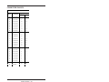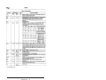
1
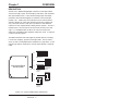
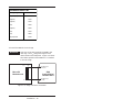
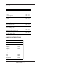
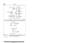
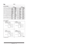
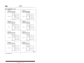
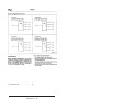
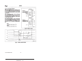
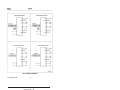
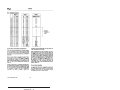
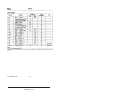
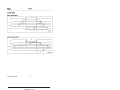
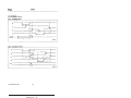
5648 User’s Manual Doc. #03764 Rev 0194 OCTAGON SYSTEMS CORPORATION® 6510 W. 91st Ave. Westminster, CO 80030 Tech. Support: 303–426–4521 COPYRIGHT Copyright 1994—Octagon Systems Corporation. All rights reserved. However, any part of this document may be reproduced, provided that Octagon Systems Corporation is cited as the source. The contents of this manual and the specifications herein may change without notice. TRADEMARKS Micro PC, PC SmartLink, Octagon Systems Corporation®, the Octagon logo and the Micro PC logo are trademarks of Octagon Systems Corporation. NOTICE TO USER The information contained in this manual is believed to be correct. However, Octagon assumes no responsibility for any of the circuits described herein, conveys no license under any patent or other right, and makes no representations that the circuits are free from patent infringement. Octagon makes no representation or warranty that such applications will be suitable for the use specified without further testing or modification. Octagon Systems Corporation general policy does not recommend the use of its products in life support applications where the failure or malfunction of a component may directly threaten life or injury. It is a Condition of Sale that the user of Octagon products in life support applications assumes all the risk of such use and indemnifies Octagon against all damage. IMPORTANT! Please read before installing your product. Octagon's products are designed to be high in performance while consuming very little power. In order to maintain this advantage, CMOS circuitry is used. CMOS chips have specific needs and some special requirements that the user must be aware of. Read the following to help avoid damage to your card from the use of CMOS chips. Using CMOS Circuitry – 1 Using CMOS Circuitry in Industrial Control Industrial computers originally used LSTTL circuits. Because many PC components are used in laptop computers, IC manufacturers are exclusively using CMOS technology. Both TTL and CMOS have failure mechanisms, but they are different. This section describes some of the common failures which are common to all manufacturers of CMOS equipment. However, much of the information has been put in the context of the Micro PC. Octagon has developed a reliable database of customer-induced, field failures. The average MTBF of Micro PC cards exceeds 11 years, yet there are failures. Most failures have been identified as customer-induced, but there is a small percentage that cannot be identified. As expected, virtually all the failures occur when bringing up the first system. On subsequent systems, the failure rate drops dramatically. ■ Approximately 20% of the returned cards are problem-free. These cards, typically, have the wrong jumper settings or the customer has problems with the software. This causes frustration for the customer and incurs a testing charge from Octagon. ■ Of the remaining 80% of the cards, 90% of these cards fail due to customer misuse and accident. Customers often cannot pinpoint the cause of the misuse. ■ Therefore, 72% of the returned cards are damaged through some type of misuse. Of the remaining 8%, Octagon is unable to determine the cause of the failure and repairs these cards at no charge if they are under warranty. The most common failures on CPU cards are over voltage of the power supply, static discharge, and damage to the serial and parallel ports. On expansion cards, the most common failures are static discharge, over voltage of inputs, over current of outputs, and misuse of the CMOS circuitry with regards to power supply sequencing. In the case of the video cards, the most common failure is to miswire the card to the flat panel display. Miswiring can damage both the card and an expensive display. ■ Multiple component failures - The chance of a random component failure is very rare since the average MTBF of an Octagon card is greater than 11 years. In a 7 year study, Using CMOS Circuitry – 2 Octagon has never found a single case where multiple IC failures were not caused by misuse or accident. It is very probable that multiple component failures indicate that they were user-induced. ■ Testing “dead” cards - For a card that is “completely nonfunctional”, there is a simple test to determine accidental over voltage, reverse voltage or other “forced” current situations. Unplug the card from the bus and remove all cables. Using an ordinary digital ohmmeter on the 2,000 ohm scale, measure the resistance between power and ground. Record this number. Reverse the ohmmeter leads and measure the resistance again. If the ratio of the resistances is 2:1 or greater, fault conditions most likely have occurred. A common cause is miswiring the power supply. ■ Improper power causes catastrophic failure - If a card has had reverse polarity or high voltage applied, replacing a failed component is not an adequate fix. Other components probably have been partially damaged or a failure mechanism has been induced. Therefore, a failure will probably occur in the future. For such cards, Octagon highly recommends that these cards be replaced. ■ Other over-voltage symptoms - In over-voltage situations, the programmable logic devices, EPROMs and CPU chips, usually fail in this order. The failed device may be hot to the touch. It is usually the case that only one IC will be overheated at a time. ■ Power sequencing - The major failure of I/O chips is caused by the external application of input voltage while the Micro PC power is off. If you apply 5V to the input of a TTL chip with the power off, nothing will happen. Applying a 5V input to a CMOS card will cause the current to flow through the input and out the 5V power pin. This current attempts to power up the card. Most inputs are rated at 25 mA maximum. When this is exceeded, the chip may be damaged. ■ Failure on power-up - Even when there is not enough current to destroy an input described above, the chip may be destroyed when the power to the card is applied. This is due to the fact that the input current biases the IC so that it acts as a forward biased diode on power-up. This type of failure is typical on serial interface chips. Using CMOS Circuitry – 3 ■ Serial and parallel - Customers sometimes connect the serial and printer devices to the Micro PC while the power is off. This can cause the failure mentioned in the above section, Failure upon power-up. Even if they are connected with the Micro PC on, there can be another failure mechanism. Some serial and printer devices do not share the same power (AC) grounding. The leakage can cause the serial or parallel signals to be 20-40V above the Micro PC ground, thus, damaging the ports as they are plugged in. This would not be a problem if the ground pin is connected first, but there is no guarantee of this. Damage to the printer port chip will cause the serial ports to fail as they share the same chip. ■ Hot insertion - Plugging cards into the card cage with the power on will usually not cause a problem. (Octagon urges that you do not do this!) However, the card may be damaged if the right sequence of pins contacts as the card is pushed into the socket. This usually damages bus driver chips and they may become hot when the power is applied. This is one of the most common failures of expansion cards. ■ Using desktop PC power supplies - Occasionally, a customer will use a regular desktop PC power supply when bringing up a system. Most of these are rated at 5V at 20A or more. Switching supplies usually require a 20% load to operate properly. This means 4A or more. Since a typical Micro PC system takes less than 2A, the supply does not regulate properly. Customers have reported that the output can drift up to 7V and/or with 7-8V voltage spikes. Unless a scope is connected, you may not see these transients. ■ Terminated backplanes - Some customers try to use Micro PC cards in backplanes that have resistor/capacitor termination networks. CMOS cards cannot be used with termination networks. Generally, the cards will function erratically or the bus drivers may fail due to excessive output currents. ■ Excessive signal lead lengths - Another source of failure that was identified years ago at Octagon was excessive lead lengths on digital inputs. Long leads act as an antenna to pick up noise. They can also act as unterminated transmission lines. When 5V is switch onto a line, it creates a transient waveform. Octagon has seen submicrosecond pulses of 8V or more. The solution is to place a capacitor, for example 0.1 µF, across the switch contact. This will also eliminate radio frequency and other high frequency pickup. Using CMOS Circuitry – 4 TABLE OF CONTENTS PREFACE ......................................................................... 1 Conventions Used In This Manual .................................................... 1 Symbols and Terminology .................................................................. 2 Technical Support ............................................................................... 3 CHAPTER 1: OVERVIEW ............................................... 5 Description .......................................................................................... 5 Major Features .................................................................................... 6 CHAPTER 2: INSTALLATION ........................................ 7 Equipment ........................................................................................... 7 Installation .......................................................................................... 7 Base Address ................................................................................ 9 Port Pinouts ................................................................................ 11 CHAPTER 3: CONTROLLING I/O LINES .................... 13 Description ........................................................................................ Port Addresses .................................................................................. Configuring I/O Lines ....................................................................... Examples .................................................................................... Pulling the I/O Lines High or Low .................................................. Access Indicator LEDs ...................................................................... Driving OPTO Module Racks ........................................................... G4 Opto–isolated Modules ........................................................ G5 Analog Modules .................................................................... Troubleshooting ................................................................................. Power Module ............................................................................. Jumper Configuration ............................................................... 13 14 15 16 17 17 17 17 18 20 20 20 CHAPTER 4: TECHNICAL DATA ................................. 21 Technical Specifications ................................................................... I/O Map .............................................................................................. Jumper Configurations ..................................................................... Connector Pinouts ............................................................................. 21 22 22 24 APPENDIX A: INTEL 82C55 DATA SHEET ................ 25 WARRANTY i PREFACE This manual is a guide to the proper configuration and operation of your 5648 Analog/Digital Interface Card. Installation instructions, card mapping information and jumpering options are described in the main body of the manual; technical specifications are included in the appendices. The 5648 card is designed to be used with any Octagon Micro PC Control Card. This combination provides a modular system which is easy to set up, modify and use. You can also use your 5648 in conjunction with other Micro PC expansion cards, allowing you to tailor your system for a wide variety of applications. CONVENTIONS USED IN THIS MANUAL 1. Information which appears on your screen (output from your system or commands or data that you key in) is shown in a different type face. Example 1: Octagon 5648 ROM BIOS Vers X.XX Copyright (c) 1993, Octagon Systems, Corp. All rights reserved Example 2: Press the <ESC> key. 2. Italicized refers to information that is specific to your particular system or program, for example, Enter filename means enter the name of your file. Names of other sections or manuals are also italicized. 3. Warnings always appear in this format: WARNING: The warning message appears here. Preface – 1 4. Paired angle brackets are used to indicate a specific key on your keyboard, for example, <ESC> means the escape key; <CTRL> means the control key; <F1> means the F1 function key. 5. All addresses are given in hexadecimal. SYMBOLS AND TERMINOLOGY Throughout this manual, the following symbols and terminology are used: W[ – ] Denotes a jumper block and the pins to connect. NOTE Information under this heading presents helpful tips for using the 5648. WARNING: Information under this heading warns you of situations which might cause catastrophic or irreversible damage. PC SmartLINK A serial communications software package designed by Octagon. It provides communications between a PC and other equipment and may be used with any PC software package, including CAMBASIC IV. Refers to all versions of PC SmartLINK. Reset Resetting the system hardware and software by pushing the reset switch. Has the same results as disconnecting power to the system, without the potential side effects of a cold reset. TTL Compatible 0–5V logic levels. H The suffix "H" denotes a hexadecimal number. For example, 1000H in hexadecimal equals 4096 in decimal. Preface – 2 TECHNICAL SUPPORT If you have a question about the 5648 Analog/Digital Interface Card and can’t find the answer in this manual, call Technical Support. They will be ready to give you the assistance you need. When you call, please have the following at hand: Your 5648 Analog/Digital Interface Card User’s Manual A description of your problem The direct line to the Technical Support is 303–426–4521. Preface – 3 This page intentionally left blank. Preface – 4 Chapter 1 OVERVIEW DESCRIPTION The Micro PC 5648 Analog/Digital Interface Card accepts switch closures and logic inputs, drives displays and LEDs, and interfaces with opto module racks. It also allows analog input and output modules to be mixed with digital I/O modules in the same opto isolator rack. Twenty–four of the 48 lines can be used for either analog or digital I/O, while the remaining 24 lines are digital I/O only. Each I/O line has a 22K pull–up resistor so that external resistors are not required when reading switch contacts. The card measures 4.5 x 4.9 inches and uses one slot of the Micro PC card cage. It is compatible with all Micro PC Control Cards and is electrically compatible with standard–sized CPU cards. It requires 5 volts at 270 mA typical. The 5648 interfaces with most types of parallel devices, including LCD and VF displays, printers and single LEDs. The I/O levels are 0–5V and are compatible with standard TTL logic levels. If the field wiring requires termination, use the STB–26 with a CMA–26 cable. OR MPB OPTO RACKS OR 5648 Analog/Digital Interface Card OR CMA–26 (4) STB–26 TERMINAL BOARD DP–IFB or LDC–IFB INTERFACE BOARD OR TBD–100 TERMINAL BOARD OR ITB TERMINAL BOARDS Figure 1–1—Typical 5648 system configuration Overview – 5 MAJOR FEATURES Driving Opto Racks The 5648 can drive up to two of the MPB–xx opto–module racks. The isolator modules are required when driving or receiving signals from high voltage and /or high current devices. Opto isolation also eliminates ground loops and significantly reduces the chance that noise will invade the system. The MPB–xx racks interface to the 5648 via CMA–26 cables. Driving Analog I/O Modules In addition to the standard digital I/O modules, the 5648 is compatible with Grayhill G5 modules. The G5 input modules produce a frequency output that is directly proportional to the input. A custom ASIC on the 5648 converts the frequency to a 0– 4095 count. The commands from the CPU card select the channel and start the conversion. The ASIC generates an interrupt on the completion of the conversion. The maximum conversion time is 625 uS. The analog modules accept thermocouples, current loop, RTD and voltage inputs. Output modules include voltage and current outputs. The ASIC measures the frequency, eliminating processor overhead. The system will detect incorrect polarity, out–of–range signal, and missing or defective module conditions. Driving Parallel Displays Adapter cables are available for driving VF and LCD series displays. Software drivers are available. You can also drive almost any parallel display. Access Indication The 5648 has two LED indicators that flash briefly when each connector group of 24 is accessed. This is useful when debugging software. Overview – 6 Chapter 2 INSTALLATION The 5648 Analog/Digital Interface Card uses one slot of the Micro PC card cage. It may be used with any Micro PC Control Card. NOTE: The G5 analog outputs will not work with the 508x Microcontrollers. The software utility disk does not apply. WARNING: The 5648 contains static sensitive CMOS components. The greatest danger occurs when the card is plugged into a card cage. The 5648 becomes charged by the user and the static discharges to the backplane from the pin closest to the card connector. If that pin happens to be an input pin, even TTL inputs may be damaged. To avoid damaging your card and its components: • • Ground yourself before handling the 5648 Digital I/O Card. Disconnect power before removing or inserting the 5648 Card. EQUIPMENT You will need the following equipment (or equivalent): • • • • • 5648 Analog/Digital Interface Card Micro PC Control Card Micro PC Card Cage Power Supply or Module PC SmartLINK or other communications software. INSTALLATION Before installing the 5648 Analog/Digital Interface Card, refer to Figure 2–1 for the location of various connectors and jumpers and Figure 2–2 for a functional diagram of the card. Installation – 7 Base Address/Interrupt Select Digital I/O Pull-up/Down Resistors W2 J1 Access Indicator W1 U13 J1 Digital I/O W3 J2 Access Indicator J2 U12 = Pin 1 Figure 2–1—5648 Component Diagram Installation – 8 Digital I/O G5 Counter Interrupt & Control Data J2 24 to 1 Mux 82C55 Port B2 W1 Interrupt Select +5 Port A2 W3 I/O Map 7 6 5 4 3 J1 Port C1 82C55 Control PC Bus Address Control Port B1 Data Data Buffer Data +5 Port A1 W2 Port C2 W1 Mux ID Figure 2–2—5648 Functional diagram Base Address The 5648 is configured at the factory to operate in most systems without any jumper changes. Jumper block W1 defines the base address. As shipped, the base address is 100H, which is jumper configuration W1[1–2, 3–4, 5–6]. If there is another card in your system with a base address of 100H, you must use a different base address for the 5648 or the other expansion card. To change the base address, change the jumper connections in block W1: Installation – 9 Base Address Select: W1 Pins Jumpered Base Address [1-2][3-4][5-6] 100H* [3-4][5-6] 110H [1-2][5-6] 120H [5-6] 130H [1-2][3-4] 140H [3-4] 150H [1-2] 160H Not jumpered 170H * = default To install the 5648 in the card cage: WARNING: Take care to correctly position the 5648 in the card cage. The VCC and ground signals must match those on the backplane. Figure 2–3 shows the relative position of the 5648 as it is installed in the card cage. A31 B31 Card Edge Pins A31 & B31 5648 Analog/Digital Interface Card Micro-PC Motherboard A1 B1 Card Edge Pins A1 & B1 Figure 2–3—Edge Connector Orientation Installation – 10 1. Verify the base address settings are correct for your application. 2. . Make sure power to the card cage is OFF 3. Slide the 5648 into the card cage. The components on the card should face to the left or up depending on the type of card cage. 4. The amber LEDs will light briefly whenever the card is accessed (input or output) at J1 or J2 PORT PINOUTS The pinouts are identical for connectors J1 and J2. Each connector has 24 I/O lines (3 ports), 5 volts and ground. The individual ports are designated A, B, and C. Port A has the lowest address; each half of port C is controllable (upper and lower C). Each port pin has a 22K pull–up/down resistor. Installation – 11 Digital I/O: J1 & J2 Pin # Function Opto Position J1 J2 19 Port A, line 0 8 8 21 Port A, line 1 9 9 23 Port A, line 2 10 10 25 Port A, line 3 11 11 24 Port A, line 4 12 12 22 Port A, line 5 13 13 20 Port A, line 6 14 14 18 Port A, line 7 15 15 10 Port B, line 0 16 16 8 Port B, line 1 17 17 4 Port B, line 2 18 18 6 Port B, line 3 19 19 1 Port B, line 4 20 20 3 Port B, line 5 21 21 5 Port B, line 6 22 22 7 Port B, line 7 23 23 13 Port C, line 0 0 0 16 Port C, line 1 1 1 15 Port C, line 2 2 2 17 Port C, line 3 3 3 14 Port C, line 4 4 4 11 Port C, line 5 5 5 12 Port C, line 6 6 6 9 Port C, line 7 7 7 2 +5V 26 Common NA NA Installation – 12 Chapter 3 CONTROLLING I/O LINES DESCRIPTION The 48 digital I/O lines on the 5648 are supplied by two 82C55 chips. The 82C55 located in U13 is connected to J1 and the 82C55 located in U12 is connected to J2. On power–up and software or hardware reset, all the digital I/O lines in J1 and J2 are configured as inputs. All lines are TTL logic level compatible (0–5V) and have 22K pull–up/down resistors to the 5V supply. The 24 digital I/O lines at J1 and J2 can be used to interface to switches, turn on low–current LEDs, and other devices that have TTL input or output (for examples, printers and scales). The STB– 26 terminal board provides a convenient way of interfacing switches or other digital I/O devices to the J1 and J2. A CMA–26 cable is used to interface the STB terminal board to the 5648. Digital I/O devices are then connected to the screw terminals on the STB–26. You can also connect opto–module racks and drive G4 opto–isolated and G5 analog modules. Figure 3–1 shows a typical terminal board and/or opto rack configuration. 1 LOGIC + – 2 3 4 5 6 7 8 9 10 J1 1 1 12 13 14 15 16 P8 J2 CMA-26 Ribbon Cable 0 5648 Digital/Analog Interface Card J1 or J2 1 2 3 4 5 6 7 MPB Opto Rack OR CMA-26 Ribbon Cable J1 J2 CMA-26 Ribbon Cable STB-26 Terminal Board Figure 3–1—Typical Terminal Board and Opto Rack Configuration Controlling I/O Lines – 13 PORT ADDRESSES Each 82C55 has three ports with eight parallel I/O lines (bits) per port. Each port has a unique I/O address. Port A and Port B can be programmed as all inputs or all outputs. Port C can be programmed in one group of eight lines (all inputs or all outputs) or as two groups of four lines (upper and lower C). The four lines in upper or lower C can each be programmed as all inputs or all outputs: 5648 Digital I/O Port: J1 and J2 Port J1 I/O Address J2 I/O Address A 1x0H 1x4H 8 lines which can be programmed as all inputs or all outputs B 1x1H 1x5H 8 lines which can be programmed as all inputs or all outputs. 8 lines interface to a high current driver. C 1x2H 1x6H 8 lines which can be programmed as one group of 8 lines or two groups of 4 lines as all inputs or all outputs. Control Register 1x3H 1x7H Description NOTE: x is the value 0-7 depending on the base address selection at W1. When a line is configured as an output, it can sink a maximum of 2.5 mA at 0.4V and can source over 2.5 mA at 2.4V. When driving opto–modules, the output can sink 15 mA at 1.0V. The 5648 uses a block of 16 addresses. Refer to the following table for the function of the associated address: Controlling I/O Lines – 14 Port Address Functions Function Port Address J1, Port A Base + 00H J1, Port B Base + 01H J1, Port C Base + 02H J1, Control Register Base + 03H J2, Port A Base + 04H J2, Port B Base + 05H J2, Port C Base + 06H J2, Control Register Base + 07H J2, G5 input start conversion, D7=1 (write); Counter Data Low (read) Base + 08H Reset Counter (write); Counter Data High (read) Base + 09H Channel Select Mux 1 of 24 (write); Channel Select Mux read back (read) Base + 0AH Status Register Interrupt, Bit 7=1; State Code, Bits 0-3; Value of 8FH=overflow Base + 0BH For a complete description of the capabilities of the 82C55, please refer to the information in Appendix A, in the Intel Peripheral Databook. Some of the chip’s capabilities are described below. CONFIGURING I/O LINES On power–up or reset, all three ports are in the input state. You can alter which ports are inputs or outputs by writing a control command to the control register in the 82C55. The examples below assume the base address is 100H. Controlling I/O Lines – 15 82C55 Control Register Commands HEX DEC Port A* Port B* Port UC* Port LC* 80H 128 OUT OUT OUT OUT 81H 129 OUT OUT OUT IN 82H 130 OUT IN OUT OUT 83H 131 OUT IN OUT IN 88H 136 OUT OUT IN OUT 89H 137 OUT OUT IN IN 8AH 138 OUT IN IN OUT 8BH 139 OUT IN IN IN 90H 144 IN OUT OUT OUT 91H 145 IN OUT OUT IN 92H 146 IN IN OUT OUT 93H 147 IN IN OUT IN 98H 152 IN OUT IN OUT 99H 153 IN OUT IN IN 9AH 154 IN IN IN OUT 9BH 155 IN IN IN IN * Ports A and B must be either all inputs of all outputs. Each half of Port C is controllable. Upper C (UC) includes bits 4 through 7 and Lower C (LC) includes bits 0 through 3. Examples The following example shows how to configure all three ports as outputs when the base address is set at 100H: OUT &H103,&H80 The following statement configures Ports A and C as input ports and B as an output port: OUT &H103, &H99 Controlling I/O Lines – 16 PULLING THE I/O LINES HIGH OR LOW Jumper block W2 pulls all of the 24 I/O lines of the J1 high or low, while W3 affects the 24 I/O lines of J2. The factory default pulls all of the I/O lines high. W2 & W3: Digital I/O Pull-up/Pull-down Resistors Pins Description Jumpered [1-2]* I/O lines pulled high [2-3] I/O lines pulled low * = default ACCESS INDICATOR LEDS Two access indicators are on the 5648, one for each connector. When the lower 24 I/O lines of J1 are accessed, the J1 LED will flash. When the upper 24 I/O lines or the G5 input module hardware is accessed the J2 LED will flash. DRIVING OPTO MODULE RACKS The 5648 can drive two MPB–8, –16 or –24 series opto module racks via a CMA–26 cable interface. To drive opto module racks, plug one end of a CMA–26 cable into one of the J connectors that you want to use and the other end into the MPB opto mounting rack. Run ground and +5V to the opto mounting rack. G4 Opto–isolated Modules You can use G4 opto–isolated modules when driving or receiving signals from high voltage and/or high current devices. Opto– isolation also eliminates ground loops and significantly reduces the chance that noise will invade the system. Use the following table to determine the corresponding opto channel for a particular 82C55 port. Remember to add the base address of the card. Controlling I/O Lines – 17 Opto Channels Channel 82C55 Port J1 Offset Address J2 Offset Address 0-3 Lower C 2 6 4-7 Upper C 2 6 8-15 A 0 4 16-23 B 1 5 For example, if the base address of the 5648 is 110H, the following would be entered into the program: reads opto rack on J2, channels 0–7 A=INP(&H116) G5 Analog Modules OUTPUT Ports A, B or C may be used on either J1 or J2 for G5 analog output. These ports must be configured as an output by writing to the control word register of the 82C55. Refer to the programming examples in the G5 directory on the 5648 utility disk for information on using G5 output modules. A file called README.DOC describes the demo programs and functions that are available in QuickBASIC and C. (Octagon’s G5 analog output driver routines momentarily disables all interrupts while in use.) NOTE: Because of strict timing requirements when updating the G5 output module, this feature is only available when the 5648 is used with the following Micro PC Control Cards: 5012, 5012A, 5025, 5025–486, 6012 and 6024. INPUT Only J2 may be used for G5 analog inputs. The frequency counter circuit used to read the G5 analog inputs is addressed at BASE + 8 through BASE + &HB. The steps for reading inputs are as follows: • • Reset frequency counter circuit Write multiplexer channel (0–23) Controlling I/O Lines – 18 • • • • Start the conversion Wait until the conversion is completed Read the counter data Convert the counter data to 12–bit count 'The following is a sample program written in QuickBASIC V4.5 'This program reads a G5 input module connected to an ‘off–card’ 'opto rack. If you run this program without a video card, substitute 'the PRINT statement with the PRINTS function included on the 5648 utility disk. The 5648 is mapped to 100H. DEFINT A–Z 'use integers where possible ZC# = 250000/9 'zero offset factor G5BASE = &H108 'base address of counter OUT &H107, &H9B 'config 8255 port C as inputs FOR X = 1 TO 1000 'take 1000 samples OUT G5BASE + 1, 0 'reset freq. counter OUT G5BASE + 2, 8 'select G5 channel #8 OUT G5BASE, &H80 'start conversion WHILE (INP(G5BASE + 3) < &H7F) 'poll until conv done WEND LSB& = INP(G5BASE) 'read count lsb MSB& = INP(G5BASE + 1) 'read count msb WORD& = LSB& + (MSB& * 256) 'form the word VALUE=INT(((ZC#-WORD&)/(WORD&/1024))+.5) 'scale value PRINT VALUE NEXT X END The conversion time will be less than 1 mS maximum. The End of Conversion may be determined either by using an interrupt or by polling the status register. In the event that a conversion is started on a channel that is not connected to a G5 module, the counting circuit will time out with a count value of 7FFFH. The data that is read is contained in 15 bits. The most significant bit of the high data byte will always be a zero. The data that is read must be converted to a numeric value in the range of 0 to 4095 as per the above program example. NOTE: The utility disk also includes software drivers that can be used to read G5 input modules. Descriptions of the drivers are included in the README.DOC file. Controlling I/O Lines – 19 You may optionally configure the 5648 to generate an interrupt at the end of each conversion (versus polling). Use the W1 jumper block to define the interrupt number. Interrupt Select: W1 Pins Jumpered Interrupt [7-8] 3 [9-10] 4 [11-12] 5 [13-14] 6 [15-16] 7 [8-10]* No interrupts * = default TROUBLESHOOTING If you have difficulty getting your system to work properly, remove all expansion cards except the 5648 Digital/Analog Interface Card from your system and check the power module and jumper configurations. Power Module The power module voltage should be 5V ±0.25V when measured at the connector pins. The power module ripple should be less than 50 mV. Jumper Configuration The 5648 is shipped with jumper connections in place for Base I/O Address 100H. Jumper changes are usually not needed to get the system running. If you changed the jumpers and the system is not working properly, return the system to the original jumper positions. If you still encounter difficulties, please contact Technical Support at 303–426–4521. Controlling I/O Lines – 20 Chapter 4 TECHNICAL DATA TECHNICAL SPECIFICATIONS The 5648 accepts switch closures and logic inputs; drives displays and LEDs; and interfaces with opto mounting racks. Each I/O line has a 22K pull–up/down resistor; external resistors are not required when using switch contacts. The 5648 will interface with most parallel devices, including LCD and DP (vacuum fluorescent) series displays, printers, and single LEDs. The I/O levels are 0–5 volts and are compatible with standard TTL logic levels. DC Characteristics Input Low: Input High: Output Low: Output High: –0.3V to +0.8V. 2V to Vcc. 0.45V maximum. 2.4V minimum. Connectors Two male 26–position, straight I/O connectors (Ansley #609–1007). Mates with Octagon CMA–26 cable. Opto Rack Interface Directly drives Octagon MPB series opto racks using CMA–26 cable. Drives G4 opto–isolated and G5 analog modules. Software Support Software drivers are provided on the 5648 utility disk. A README.DOC text file explains the driver usages. Bus Compatibility Electrically compatible with the PC bus; designed to be used in the Micro PC card cage with Octagon’s Micro PC Control Cards. May be used with AT–sized PC’s if used in conjunction with adapter bracket. Power Requirements 5V +/– 5% at 270 mA typical, 300 mA maximum. Environmental –40° to 70° C operating temperature; –50 ° to 85° C nonoperating 5 to 95% RH, noncondensing Size 4.5 in. x 4.9 in. Technical Data – 21 I/O MAP Port Address Functions Function Port Address J1, Port A Base + 00H J1, Port B Base + 01H J1, Port C Base + 02H J1, Control Register Base + 03H J2, Port A Base + 04H J2, Port B Base + 05H J2, Port C Base + 06H J2, Control Register Base + 07H J2, G5 input start conversion, D7=1 (write); Counter Data Low (read) Base + 08H Reset Counter (write); Counter Data High (read) Base + 09H Channel Select Mux 1 of 24 (write); Channel Select Mux read back (read) Base + 0AH Status Register Interrupt, Bit 7=1; State Code, Bits 0-3; Value of 8FH=overflow Base + 0BH JUMPER CONFIGURATIONS Base Address Select: W1 Pins Jumpered Base Address [1-2][3-4][5-6] 100H* [3-4][5-6] 110H [1-2][5-6] 120H [5-6] 130H [1-2][3-4] 140H [3-4] 150H [1-2] 160H Not jumpered 170H * = default Technical Data – 22 Interrupt Select: W1 Pins Jumpered Interrupt [7-8] 3 [9-10] 4 [11-12] 5 [13-14] 6 [15-16] 7 [8-10]* No interrupts * = default W2 & W3: Digital I/O Pull-up/Pull-down Resistors Pins Description Jumpered [1-2]* I/O lines pulled high [2-3] I/O lines pulled low * = default Technical Data – 23 CONNECTOR PINOUTS Digital I/O: J1 & J2 Opto Position Pin # Function 19 Port A, line 0 21 Port A, line 1 9 9 23 Port A, line 2 10 10 25 Port A, line 3 11 11 24 Port A, line 4 12 12 22 Port A, line 5 13 13 20 Port A, line 6 14 14 18 Port A, line 7 15 15 10 Port B, line 0 16 16 8 Port B, line 1 17 17 4 Port B, line 2 18 18 6 Port B, line 3 19 19 1 Port B, line 4 20 20 3 Port B, line 5 21 21 5 Port B, line 6 22 22 7 Port B, line 7 23 23 13 Port C, line 0 0 0 16 Port C, line 1 1 1 15 Port C, line 2 2 2 17 Port C, line 3 3 3 14 Port C, line 4 4 4 11 Port C, line 5 5 5 12 Port C, line 6 6 6 9 Port C, line 7 7 7 2 +5V 26 Common NA NA J1 J2 8 8 Technical Data – 24 Appendix A Intel 82C55 Data Sheet INTEL 82C55A DATA SHEET The material in this appendix is Copyright 1992, Intel Corporation. Appendix A – 25 Appendix A – 26 Appendix A – 27 Appendix A – 28 Appendix A – 29 Appendix A – 30 Appendix A – 31 Appendix A – 32 Appendix A – 33 Appendix A – 34 Appendix A – 35 Appendix A – 36 Appendix A – 37 Appendix A – 38 Appendix A – 39 Appendix A – 40 Appendix A – 41 Appendix A – 42 Appendix A – 43 Appendix A – 44 Appendix A – 45 Appendix A – 46 Appendix A – 47 Appendix A – 48 WARRANTY Octagon Systems Corporation (Octagon), warrants that its standard hardware products will be free from defects in materials and workmanship under normal use and service for the current established warranty period. Octagon’s obligation under this warranty shall not arise until Buyer returns the defective product, freight prepaid to Octagon’s facility or another specified location. Octagon’s only responsibility under this warranty is, at its option, to replace or repair, free of charge, any defective component part of such products. LIMITATIONS ON WARRANTY The warranty set forth above does not extend to and shall not apply to: 1. 2. 3. Products, including software, which have been repaired or altered by other than Octagon personnel, unless Buyer has properly altered or repaired the products in accordance with procedures previously approved in writing by Octagon. Products which have been subject to power supply reversal, misuse, neglect, accident, or improper installation. The design, capability, capacity, or suitability for use of the Software. Software is licensed on an “AS IS” basis without warranty. The warranty and remedies set forth above are in lieu of all other warranties expressed or implied, oral or written, either in fact or by operation of law, statutory or otherwise, including warranties of merchantability and fitness for a particular purpose, which Octagon specifically disclaims. Octagon neither assumes nor authorizes any other liability in connection with the sale, installation or use of its products. Octagon shall have no liability for incidental or consequential damages of any kind arising out of the sale, delay in delivery, installation, or use of its products. SERVICE POLICY 1. 2. 3. Octagon’s goal is to ship your product within 5 working days of receipt. If a product should fail during the warranty period, it will be repaired free of charge. For out of warranty repairs, the customer will be invoiced for repair charges at current standard labor and materials rates. Customers that return products for repairs, within the warranty period, and the product is found to be free of defect, may be liable for the minimum current repair charge. RETURNING A PRODUCT FOR REPAIR Upon determining that repair services are required, the customer must: 1. 2. 3. 4. 5. 6. 7. Obtain an RMA (Return Material Authorization) number from the Customer Service Department, 303-430–1500. If the request is for an out of warranty repair, a purchase order number or other acceptable information must be supplied by the customer. Include a list of problems encountered along with your name, address, telephone, and RMA number. Carefully package the product in an antistatic bag. (Failure to package in antistatic material will VOID all warranties.) Then package in a safe container for shipping. Write RMA number on the outside of the box. For products under warranty, the customer pays for shipping to Octagon. Octagon pays for shipping back to customer. Other conditions and limitations may apply to international shipments. NOTE: PRODUCTS RETURNED TO OCTAGON FREIGHT COLLECT OR WITHOUT AN RMA NUMBER CANNOT BE ACCEPTED AND WILL BE RETURNED FREIGHT COLLECT. RETURNS There will be a 15% restocking charge on returned product that is unopened and unused, if Octagon accepts such a return. Returns will not be accepted 30 days after purchase. Opened and/or used products, non-standard products, software and printed materials are not returnable without prior written agreement. GOVERNING LAW This agreement is made in, governed by and shall be construed in accordance with the laws of the State of Colorado. The information in this manual is provided for reference only. Octagon does not assume any liability arising out of the application or use of the information or products described in this manual. This manual may contain or reference information and products protected by copyrights or patents. No license is conveyed under the rights of Octagon or others.