1
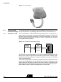
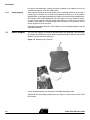
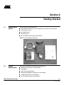
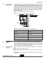
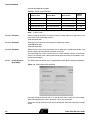
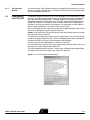
JTAG ICE
.....................................................................
User Guide
Table of Contents
Table of Contents
Section 1
Introduction ........................................................................................... 1-1
1.1
1.2
1.3
Features ....................................................................................................1-1
JTAG ICE and the OCD Concept .............................................................1-2
1.2.4.1
Software Breakpoints ...................................................................1-3
1.2.4.2
Hardware Breakpoints..................................................................1-3
Device Support .........................................................................................1-4
Section 2
Getting Started...................................................................................... 2-1
2.1
2.2
2.3
2.4
Unpacking the System ..............................................................................2-1
System Requirements...............................................................................2-1
Connecting JTAG ICE...............................................................................2-2
Connecting Power.....................................................................................2-3
Section 3
Frontend Software ................................................................................ 3-1
3.1
3.2
Installing AVR Studio ................................................................................3-1
On-chip Debugging with JTAG ICE ..........................................................3-1
3.2.3.1
Run Timers in Stopped Mode ......................................................3-3
3.2.3.2
OCD communication frequency ...................................................3-3
3.2.5.1
Breakpoint Option 1 .....................................................................3-4
3.2.5.2
Breakpoint Option 2 .....................................................................3-4
3.2.5.3
Breakpoint Option 3 .....................................................................3-4
3.2.6.1
Data Memory Breakpoints............................................................3-4
3.2.6.2
Masked Breakpoint ......................................................................3-4
3.2.6.2.1
Example 1..............................................................................3-6
3.2.6.2.2
Example 2..............................................................................3-6
3.2.6.2.3
Example 3..............................................................................3-6
3.2.6.3
3.3
Enable Break on Branch/Skip ......................................................3-6
Programming with JTAG ICE ....................................................................3-7
Section 4
Special Considerations ......................................................................... 4-1
4.1
4.2
4.3
I/O Peripherals ..........................................................................................4-1
Single Stepping.........................................................................................4-1
Software Breakpoints ................................................................................4-1
iii
Table of Contents
4.4
4.5
4.6
4.7
4.8
4.9
4.10
4.11
Target AVR Reset and Power Down during Debugging ...........................4-2
JTAG Relevant Fuse Settings...................................................................4-2
Use AVR Studio 3.52 or Higher ................................................................4-2
The Message Window ..............................................................................4-2
JTAG ICE Does not Support Devices in a JTAG Chain............................4-2
Accessing I/O Registers............................................................................4-2
Alternative JTAG Pin Functions when Using the JTAG Interface .............4-2
Verifying the Flash ....................................................................................4-2
Section 5
Hardware Description ........................................................................... 5-1
5.1
5.2
5.3
5.4
5.5
5.6
General Board Description........................................................................5-1
Communication Module ............................................................................5-1
Control Module..........................................................................................5-2
Level Converters .......................................................................................5-2
Power Supply ............................................................................................5-4
JTAG Adapter ...........................................................................................5-4
Section 6
Technical Specifications ....................................................................... 6-1
Section 7
Technical Support................................................................................. 7-1
iv
Section 1
Introduction
Congratulations on purchasing Atmel’s AVR® JTAG ICE. The JTAG ICE is a complete
tool for On-chip Debugging on all AVR 8-bit microcontrollers with the JTAG interface.
The JTAG interface is a 4-wire Test Access Port (TAP) controller that is compliant with
the IEEE 1149.1 standard. The IEEE standard was developed to enable a standard way
to efficiently test circuit board connectivity (Boundary Scan). Atmel AVR devices have
extended this functionality to include full Programming and On-chip Debugging support.
The JTAG ICE uses the standard JTAG interface to enable the user to do real-time
emulation of the microcontroller while it is running in the target system.
The AVR On-chip Debug protocol (AVROCD) gives the user complete control of the
internal resources of the AVR microcontroller. The JTAG ICE provides emulation capability at a fraction of the cost of traditional emulators.
1.1
Features
AVR Studio® Compatible
Supports all AVR Devices with JTAG Interface
Exact Electrical Characteristics
Emulates all Digital and Analog On-chip Functions
Break on Change of Program Flow
Data and Program Memory Breakpoints
Suports Assembler and HLL Source Level Debugging
RS-232 Interface to PC for Programming and Control
Regulated Power Supply for 9-15V DC Power
The JTAG ICE is supported by AVR Studio version 3.52 or higher. For up to date information on this and other AVR tool products please read the document “avrtools.pdf”.
The latest version of AVR Studio, “avrtools.pdf” and this user guide can be found in the
AVR section of the Atmel web site, www.atmel.com.
AVR® JTAG ICE User Guide
1-1
Rev. 2475A-09/01
Introduction
Figure 1-1. The JTAG ICE
1.2
JTAG ICE and
This chapter will explain the concept of On-chip Debugging (OCD) used by the JTAG
the OCD Concept ICE and explain how On-chip Debugging differs from other In-circuit Emulator (ICE).
1.2.1
Emulation vs. OCD
An In-circuit Emulator is a device built to emulate the behavior of a single device or a
group of devices. For example, if emulating an ATmega323, the emulator hardware tries
to imitate the exact behavior of this device. The closer this behavior is to the actual
device the better the emulation will be. Figure 1-2 shows a simplified block diagram of
this traditional emulator approach.
Figure 1-2. Traditional Emulator Block Diagram
Emulator
Logic
Programmed
to Behave
Like the
Device
PROBE
Software
Frontend
(AVR Studio)
Target Board
The JTAG ICE uses a different approach. The JTAG ICE interfaces the internal On-chip
Debug system inside the target AVR, and provides an interface and a method for monitoring and controlling the execution in a physical AVR device through the JTAG IEEE
1149.1 compliant interface.
The way the JTAG ICE works is as follows: In all AVR devices with JTAG interface there
is built-in On-chip Debug logic that the JTAG ICE will interface. This OCD logic can be
used to control the execution in the device. So while a traditional Emulator emulates
device behavior, the JTAG ICE will take control of the device and execute the code in a
physical device. Figure 1-3 shows a block diagram of an OCD system.
1-2
AVR® JTAG ICE User Guide
Introduction
Figure 1-3. JTAG ICE Interfacing the Internal AVR OCD System
PCB
JTAG ICE
Interfacing
the Real
Device
AVR
Software
Frontend
(AVR Studio)
Exact electrical and timing characteristics are achieved by using the OCD system. On
the other hand, a traditional Emulator may provide additional control of the internal
resources of the device. Trace buffer is not implemented on the AVR OCD system.
Note: Some restrictions apply. See the “Special Considerations” section for more
information.
When debugging code, it is important to be aware of the way the JTAG ICE operates. In
the following subsections, some considerations will be explained.
1.2.2
Run Mode
In Run mode, the code execution is completely independent of the JTAG ICE. The
JTAG ICE will continuously poll the target AVR to see if a break condition has occurred.
When this happens, the OCD system will read out all necessary data Program Counter,
I/O registers, EEPROM, General Purpose registers, and SRAM contents, and transmit
this to AVR Studio through the JTAG interface. Since the target AVR device operates
independently, there is no way of tracing what code has been executed prior to the
breakpoint.
1.2.3
Stopped Mode
When a breakpoint is reached, the program execution is halted, but all I/O will continue
to run as if a breakpoint did not occurred. For example, assume that a USART transmit
was initiated when a breakpoint is reached. Using a traditional ICE, the operation would
be halted, and single stepping through the code would give a cycle accurate bit pattern
on the TxD pin. When using the JTAG ICE on the AVR, the USART would continue to
run at full speed completing the transmission.
1.2.4
Breakpoints
The AVR OCD system distinguishes between two types of breakpoints; software and
hardware breakpoints.
1.2.4.1
Software
Breakpoints
A software breakpoint is a break instruction placed in Flash memory. When this instruction is executed, it will break the program execution. When placing a breakpoint on an
instruction in AVR Studio, this instruction is physically rewritten as a break instruction in
the AVR Flash memory. When reaching this instruction the operation is halted. To continue execution a “start” command has to be given from the OCD logic. When starting
the execution, the instruction replaced by software break instruction is executed before
continuing to execute instructions from the Flash memory.
1.2.4.2
Hardware
Breakpoints
In the OCD logic there are 4 registers capable of storing one memory address each. The
JTAG ICE uses one of these registers permanently to implement single stepping. The 3
others can be combined to generate valid break conditions. Section 3.2.4 describes in
detail the different ways of combining these registers.
Software breakpoint require reprogramming of the entire page, hardware breakpoints
are recommended for breakpoints that are often modified.
1.2.5
I/O Registers
JTAG ICE has limitation in viewing the contents in all I/O locations.
When an AVR device reaches a breakpoint, the contents of all I/O registers are read out
and presented in AVR Studio. Reading alters the contents in some registers, these registers will not be read (e.g., Reading USART data register, will clear the RXC bit). See
AVR® JTAG ICE User Guide
1-3
Introduction
the “Special Considerations” section to find the complete list of registers that not are
accessible through the JTAG ICE OCD system.
1.2.6
Single Stepping
Some registers needs to be read or written within a specified number of cycles after a
control signal is enabled. The I/O clock and peripherals continue to run at full speed in
stopped mode, single stepping through such code will not meet the timing requirements.
For example, when single stepping, the I/O clock might have run for millions of cycles.
To read or write registers with such timing requirements, the read or write sequence
should be performed as a single operation. Run the device at full speed by using a
macro, function call or run-to-cursor.
For detailed information about the “JTAG Interface and On-chip Debug System” see the
applicable datasheet.
1.3
Device Support
The JTAG ICE supports all AVR 8-bit Microcontrollers with integrated JTAG functionallity. Support for new devices will be added through AVR Studio. Latest version of AVR
Studio is available from www.atmel.com.
Figure 1-4. Emulating with JTAG ICE
A list of supported devices can be found in the AVR Studio help system.
AVR Studio will automatically prompt the user if there is a newer version of the JTAG
ICE firmware.
1-4
AVR® JTAG ICE User Guide
Section 2
Getting Started
2.1
Unpacking the
System
The box contains the following items:
JTAG ICE with Flexcable and a JTAG Adapter Card with two 10-pin connectors
JTAG ICE User Guide
9-pin RS232 Cable
DC Power Cable
Atmel CD-ROM with Datasheets and Software
Figure 2-1. Unpacking the JTAG ICE
2.2
System
Requirements
The minimum hardware and software requirements are:
486 Processor (Pentium is recommended)
AVR® JTAG ICE User Guide
16 MB RAM
16 MB Free Hard Disk Space
Windows® 95/98/2000, or Windows NT® 4.0 or Higher
115200 Baud RS-232 Port (COM Port)
9-15V DC Power Supply, 60 mA Minimum.
2-1
Rev. 2475A-09/01
Getting Started
2.3
Connecting
JTAG ICE
Before starting AVR Studio, the JTAG ICE must be connected to the front-end PC and
target board. All connections must be made before starting AVR Studio to ensure correct auto-detection by AVR Studio.
2.3.1
Connecting JTAG
ICE to PC
JTAG ICE uses a standard RS-232 port for communication. Connect the RS-232 cable
between the JTAG ICE and a free COM port on the PC. AVR Studio will automatically
search through the available COM ports and detect supported tools.
If other devices control the COM ports, they must be shut down before starting AVR Studio. AVR Studio cannot gain control of a COM port if other resources have control of the
port (e.g., Modem, IrDA, PDA etc.).
2.3.2
Connecting JTAG
ICE to Target Board
A minimum of 6 wires are required to connect JTAG ICE to the target board. These signals are TCK, TDO, TDI, TMS, VTref and GND.
Optional lines are: Vsupply and the nSRST. The nTRST signal is not used, and is
reserved for compatibility with other equipment.
Vsupply should be used if target board supplies power to the JTAG ICE.
nSRST is used to control and monitor the target reset line. However, this is not
necessary for emulation. If the application code sets the JTD bit in the MCUCSR, the
JTAG Interface will be disabled. To enable the JTAG ICE to reprogram the target
AVR, it will need to control of the Reset Pin.
The following examples will assume a 6-wire connection between target and JTAG ICE
(shown with solid lines in Figure 2-2).
Figure 2-2 shows which JTAG lines should be connected to the target AVR to ensure
correct operation. To avoid drive contention on the lines, place series resistors between
the JTAG lines and external circuitry. The value of the resistor should not exceed the
maximum ratings and sink or source to much current. See Section 5.4 for a detailed
description of the hardware.
Note: The JTAG ICE does not support several devices placed into a JTAG Chain. For
example, the target AVR must be the only device connected to the JTAG ICE.
Figure 2-2. Connecting JTAG ICE to Target Board
LOAD
2-2
TCK
TD0
TMS
TDI
VCC
GND
Target AVR
1
TCK
3
TD0
5
TMS
9
TDI
4
VTref
GND 2/10
7
Vsupply
6
nSRST
8
nTRST
RST
AVR® JTAG ICE User Guide
Getting Started
2.3.3
Connecting JTAG
ICE to STK500
The STK500 does not have a dedicated JTAG interface connector. To connect the
JTAG ICE to the STK500 board. The included STK500 JTAG adapter can be used. This
adapter supports the ATmega323, ATmega32, and ATmega16. Alternatively, the JTAG
Probe must be strapped to the appropriate JTAG Port pins of the target device. Check
the target device datasheet for the location of the JTAG pins on the appropriate device.
Figure 2-3 shows an example on how the pins should be connected for an ATmega323.
Remember to remove the reset jumper on the STK500 if the reset pin is going to be controlled from the JTAG ICE.
Note: The STK501 does have a dedicated JTAG connector.
Figure 2-3. Connecting JTAG ICE to STK500 with ATmega323
STK500
Port C
PC1 PC3 PC5 PC7 VTG
PC0 PC2 PC4 PC6 GND
5
6
3
4
STK500
Port E
(TCK)
7
8
(TD0)
(TMS)
(TDI)
9
JTAG
Connector 10
RST
1
2
(GND)
(VTG)
(nSRST)
Table 2-1. Connecting JTAG ICE to STK500 with an ATmega323
JTAG Probe
STK500
TCK (Pin 1)
PC2 (Port C)
TDO (Pin 3)
PC4 (Port C)
TMS (Pin 5)
PC3 (Port C)
TDI (Pin 9)
PC5 (Port C)
VTref (Pin 4)
VTG
GND (Pin 2)
GND
nSRST (Pin 6)
RST (Port E)
2.4
Connecting
Power
The JTAG ICE power supply can operate using either an external power supply, or it
can be supplied directly from the target board. The power connector works like a switch
when choosing between using external or target power. If no external power supply is
connected, the board will use the target board as power source. If an external power
supply is connected, this will be used instead of the target.
2.4.1
Power from Target
Application
When the JTAG ICE is supplied with power from the target VDD some considerations
apply:
Target voltage has to be from 3V to 5.5V.
Target must be able to supply at least 220 mA @ 3.3V or 120 mA @5.5V to the JTAG
ICE.
If these requirements cannot be met, an external power supply should be connected to
the JTAG ICE.
AVR® JTAG ICE User Guide
2-3
Getting Started
Always use an external power supply for the JTAG ICE, if the target power will be cycled
during debugging.
2.4.2
Using External
Power Supply
Voltage range for the external power supply is shown in Table 2-2.
Table 2-2. Voltage Range for the External Power Supply
Power Requirements
Min
Max
Units
Target VDD Voltage range when supplying the JTAG
ICE
3.3
5.5
V
Total target VDD Voltage Range
1.8
6
V
Target VDD current capability when supplying the
JTAG ICE
120 (@5.5V)
220 (@3.3V)
mA
External Power Supply Range DC
9 (@50 mA)
15 (@60 mA)
VDC
External Power Supply Range AC
9
9
VAC
When the JTAG ICE is connected the PC and target board, power may be turned on.
The following power up sequence is recommended to ensure proper communication
between target AVR, JTAG ICE and AVR Studio.
1. Power up Target board
2. Power up JTAG ICE
3. Start up AVR Studio
If target board is supplying power to JTAG ICE, it will automatically be powered up correctly when powering up the target board.
Figure 2-4. Connecting Power
AVR
STUDIO
RS-232
2
1
Power Up
JTAG ICE
3
Start
AVR Studio
Power Up
Target
The equipment will not be harmed using a different power up sequence, but communication problems between AVR Studio and the JTAG ICE may occure.
If this happens use the recommended power up sequence.
2-4
AVR® JTAG ICE User Guide
Section 3
Frontend Software
This section will cover all special features and considerations when using On-chip
Debugging with AVR Studio and JTAG ICE. General AVR Studio topics are covered in
the AVR Studio online help system.
3.1
Installing AVR
Studio
AVR Studio with its Integrated Development Environment (IDE) is the ideal software for
all AVR development. It has an editor, an assembler and a debugger and is the frontend for all AVR emulators and the JTAG ICE.
To install AVR Studio insert the supplied Atmel CD-ROM in the computer and use your
browser to navigate to “Products → AVR 8-bit RISC → Software”. Right click with the
mouse on the “AVRstudio3.exe” file and select “save link as”. Select an empty directory
and save the file. Execute the “AVRstudio3.exe” file. This is a self-extracting file that will
extract all required files to the current directory. Execute the “Setup.exe” file. This file will
guide you through the setup process.
Note:
AVR Studio version 3.51 or later is required for JTAG ICE support.
The latest release of AVR Studio can be found in the AVR section of the Atmel website,
www.atmel.com.
3.2
On-chip
Debugging with
JTAG ICE
It is assumed that the reader has general knowledge of how to use the AVR Studio software. For more information on general use of AVR Studio, please look in the interactive
help system supplied with AVR Studio. This section covers JTAG ICE specific topics
only.
3.2.1
Connecting System
Figure 2-4 explains how to connect the system for proper communication between target board, JTAG ICE and AVR Studio.
3.2.2
Starting Software
When the system is correctly connected and powered up, AVR Studio should be
launched. Open a project and AVR Studio will search the COM ports for the JTAG ICE.
Note that AVR Studio searches through the COM ports in a sequential manner. If other
Atmel tools are connected to COM ports, make sure that these are switched off, or disconnected, as AVR studio will look for supported AVR tools, and connect to the first tool
it finds.
Note:
AVR® JTAG ICE User Guide
Make sure no other devices or applications have control of the selected COM
port.
3-1
Frontend Software
The JTAG ICE will then detect if there is power on the target board. If there is power the
JTAG ICE will read the JTAG ID (Identification Number) on the target AVR. If the JTAG
ICE fails to read the JTAG ID it could be that:
1. The target AVR is not connected to the JTAG ICE.
Solution: Verify that the JTAG ICE is correctly connected to the target AVR.
2. The JTAG Interface fuse is not enabled on the target AVR.
Solution: Use another interface (e.g., ISP) to verify that the JTAG fuse set enables.
3. The JTAG Interface fuse is enabled, but the existing application on the target
AVR has set the JTD (JTAG Disable) bit in the MCUCSR register.
Solution: Hold the target AVR in Reset will prevent the JTD bit from being set by the
application code. If the Reset line on the target AVR is connected to the JTAG ICE,
the JTAG ICE can hold the Reset line during the reprogramming as long as the Hold
Reset option is selected.
When the JTAG ID is read successfully, the JTAG ICE will read the lock bit settings. If
the lock bits are set the JTAG ICE has to do a Chip Erase on the target AVR before
proceeding.
The JTAG ICE will then automatically enable the On-chip Debug fuse on the target
AVR. Note that the JTAG ICE will automatically disable the OCD fuse, when the debugging session is finished and the project is closed.
AVR Studio will then present the dialog in Figure 3-1.
Figure 3-1. Options Dialog Shown Prior to the Chip Erase and Programming of the
Target AVR
To ensure proper communication between the JTAG ICE and the target AVR, the OCD
communication frequency from the JTAG ICE must be equal or less than 1/4 of the target AVR frequency.
There is also an option to change the actual state of the "preserve eeprom bit" setting on
the target AVR before the JTAG ICE executes a Chip Erase.
After executing a Chip Erase on the target AVR, the JTAG ICE will release the Reset
line if it had previously tied it down.
The code will then be downloaded into the flash. Note that for speed optimization, the
flash programming is not verified at this stage.
Based on the JTAG ID from the target AVR, AVR Studio will configure the correct I/O
view and settings accordingly.
3.2.3
3-2
On-chip Debugger
Options
To access the On-chip Debugger Options while debugging use the menu option:
Options →=On-chip Debugger Options.
AVR® JTAG ICE User Guide
Frontend Software
Figure 3-2. On-chip Debugger Options
3.2.3.1
Run Timers in
Stopped Mode
This mode allows the timers to continue running at their normal speed when single stepping through the code. When this box is not checked, the timers will be increased cycle
accurate to the stepping through the code.
Press “Connection Options” to enter On-chip Debugger Connection Options.
3.2.3.2
OCD communication
frequency
It is important that the OCD communication frequency is set to be maximum 1/4 of the
frequency of the target AVR. If the JTAG ICE communicates at a higher speed, than the
target AVR; communication will fail. If the user specifies an OCD frequency that is too
low, communication will work, but unnecessary delays are introduced.
There is also an option to change the actual state of the preserve EEPROM bit setting
on the target AVR.
3.2.4
Hardware
Breakpoints
JTAG ICE has a unique breakpoint system that supports breakpoints.
JTAG ICE has a limited number of hardware breakpoints. The 3 general-purpose hardware breakpoints are available. In addition there is a special “break on change of
program flow” option, which can be enabled.
The 3 general-purpose hardware breakpoints can be used as:
3 general-purpose breakpoints
2 general-purpose breakpoints and 1 data breakpoint
1 general-purpose breakpoint and 2 data breakpoints
1 general-purpose breakpoint and 1 masked SRAM breakpoint
1 general-purpose breakpoint and 1 masked Flash breakpoint
Break on change of program flow can be enabled or disabled regardless of which other
breakpoint options are used.
AVR Studio will track modes, and will give a warning if too many breakpoints are set.
Note:
3.2.5
Software
Breakpoints
The JTAG documentation states that 4 breakpoints are available. One breakpoint is permanently reserved for single-step, giving the user 3 breakpoints for
general use.
Some AVR devices support break instructions. Using break instructions means that the
actual instruction is replaced by a break instruction in the Flash memory during debugging. By using break instructions an unlimited number of breakpoints can be used. Since
the actual instruction is replaced by a break instruction, the flash page has to be reprogrammed when adding or removing a breakpoint.
The break instructions are slower than hardware breakpoints
Three different options regarding breakpoints are available:
Automatic, but prefer hardware breakpoints
Only use hardware breakpoints
Only use break instructions
AVR® JTAG ICE User Guide
3-3
Frontend Software
Note:
Software breakpoints will not work on the ATmega128 if it is set to operate in
ATmega103 compatibility mode. That is because the ATmega103 does not support the SPM Instruction.
3.2.5.1
Breakpoint Option 1
In “automatic, but prefer hardware breakpoints mode”, AVR Studio will analyze the
breakpoints, and try to place the hardware breakpoints and the Break Instructions in an
optimum manner.
3.2.5.2
Breakpoint Option 2
Using the “only use hardware breakpoints” option, only the 3 general purpose breakpoints are available. This is the default mode, and the only available mode for devices
without break instruction support in JTAG ICE.
3.2.5.3
Breakpoint Option 3
The “only use break instructions” mode forces AVR Studio to only use break instructions. No hardware breakpoints will be used.
Note:
It is recommended to use one of the two other.
3.2.6
General-purpose
Breakpoints
A general-purpose breakpoint can be placed anywhere in program code. The JTAG ICE
supports source level debugging, and breakpoints can be placed on any assembly or
HLL statement in the code. The AVR will break before executing the “break” instruction.
3.2.6.1
Data Memory
Breakpoints
The data memory breakpoints can be set to one of three modes; Data memory Read,
Data memory Write or Data memory Read or Write. Data breakpoints will work in I/O
memory, and SRAM only. It is not possible to set breakpoints in the Register file.
In order to use variable names (e.g., PORTB), the object file needs to include symbolic
information. Using symbolic variables is possible if using a C-compiler, or an assembler
that includes symbolic information (e.g., EWBAVR, ICCAVR, IAR Assembler).
The assembler provided with AVR Studio does not provide symbolic information.
When using Data breakpoints, the AVR will break after executing the instruction causing
the break condition.
Figure 3-3. Data Breakpoints
3.2.6.2
3-4
Masked Breakpoint
When masked breakpoints are enabled the user must specify the Address base and
Address mask. The two registers are bit wise AND’ed together to generate valid break
conditions. This value is compared to the masked Program Counter or Data Address to
see if a valid break condition is present.
AVR® JTAG ICE User Guide
Frontend Software
Figure 3-4. Masked Breakpoints
By setting a bit position in the mask to zero, that bit position will be don’t care and will
generate a valid break regardless if that bit position in the PC or data address is high or
low.
By setting a bit position in the mask to one, that bit position will be “locked” so that the
corresponding bit position in the PC or data address must be at the same logic level as
the bit position in the base address. Figure 3-5 shows the block diagram of how this is
implemented.
Figure 3-5. Masked Breakpoints Block Diagram
MASK
&
BASE
=1
PC
DATA ADR.
0
&
1
Valid Instr.
MEMTYPE
RD
BRK
WR
BREAK ON
AVR® JTAG ICE User Guide
3-5
Frontend Software
Consider the following examples:
Table 3-1. Break Vector Examples
#
Address Base
Address Mask
Break Vectors
# Break
Vectors
1
1010 1010 0101 0101
1111 1111 1111 1111
1010 1010 0101 0101
20 = 1
2
1010 1010 0101 0101
1111 1101 1111 1111
1010 10x0 0101 0101
21 = 2
3
1010 1010 0101 0101
1111 0000 1111 1111
1010 xxxx 0101 0101
24 = 16
4
1010 1010 0101 0101
1010 1010 0101 0101
1x1x 1x1x x0x0 x0x0
28 = 256
5
1010 1010 0101 0101
0000 0000 0000 0000
xxxx xxxx xxxx xxxx
216 = 65536
Note:
3.2.6.2.1 Example 1
x = don’t cares
Setting all high in the Mask, will result that only the base address will generate a valid
break vector. Only valid Break vector is:
1010 1010 0101 0101
3.2.6.2.2 Example 2
Setting bit 9 in the Mask to zero will give two valid break vectors:
1010 1000 0101 0101
1010 1010 0101 0101
3.2.6.2.3 Example 3
Setting all bits in the mask to zero means that all addresses are valid break vectors, and
will thus single step the AVR one instruction at the time.
The control logic will cause a break if the PC or Data address matches a valid break
vector. The AVR will cause a break after executing the instruction on the address causing the break condition.
3.2.6.3
Enable Break on
Branch/Skip
The “Enable break on branch/skip” is independent of the 3 general-purpose breakpoints.
Figure 3-6. Enable Break on Branch/Skip
A change of program memory flow is as any deviation from a linear flow, for example,
when executing interrupts, jumps, branches, calls or skip instructions.
A break on change of flow will break after executing the instruction causing the change
of flow.
3-6
AVR® JTAG ICE User Guide
Frontend Software
3.2.7
The Processor
Window
The Cycle Counter, Time Elapsed, Frequency and StopWatch functionality is not available when using the JTAG ICE. This is a direct result of the nature of the implementation
of the On-chip Debug functionality.
3.3
Programming
with JTAG ICE
In addition to using the JTAG ICE as an On-chip Debugger, it can also be used as a programmer. The JTAG programming interface is an extension to the familiar STK500 software. Activate the menu option Tools → STK500 to open the programming interface.
AVR Studio will search the COM ports for the JTAG ICE. Note that AVR Studio searches
through the COM ports in a sequential manner. If other Atmel tools are connected to
COM ports, make sure that these are switched off, or disconnected, as AVR studio will
look for supported AVR tools, and connect to the first tool it finds.
Make sure no other device or application controls the selected COM port, and that there
are no active debugging sessions using the JTAG ICE.
Caution: If you disable the JTAG Enable fuse you will not be able to communicate with
the target AVR with the JTAG ICE.
To ensure correct programming when using the JTAG interface, the user must perform
a Chip Erase before programming the Flash or EEPROM. Remember to disable the
“Preserve EEPROM” fuse if you intend to reprogram the EEPROM.
The DOS version of the STK500 does not support the JTAG ICE.
For more information on general use of the programming interface, please look in the
interactive help system supplied with AVR Studio.
The JTAG programming user interface is similar to the STK500 programming software,
but displays JTAG ICE in the header if the JTAG ICE is detected
Figure 3-7. The JTAG Programming Interface
AVR® JTAG ICE User Guide
3-7
Frontend Software
3-8
AVR® JTAG ICE User Guide
Section 4
Special Considerations
When using the JTAG ICE some special considerations should be noted.
4.1
I/O Peripherals
All I/O peripherals will continue to run even though the program execution is stopped by
a breakpoint. Example: If a breakpoint is reached during a UART transmission, the
transmission will be completed and corresponding bits set. The transmit complete (TXC)
flag will be set and will be available on the next single step of the code even though it
normally would happen later in an actual device.
All I/O modules will continue to run in stopped mode with the following two exceptions:
Timer/Counters
Watchdog Timer
4.1.1
Timer/Counters in
Stopped Mode
From the On-chip Debugging options menu the user can decide if the Timer/Counters
should continue to run in stopped mode, or if they should be stopped.
4.1.2
Watchdog Timer
The watchdog timer will be halted in stopped mode. This avoids an unintentional AVR
reset during stopped mode.
4.2
Single Stepping
The I/O continues to run in stopped mode, avoid timing even though the program execution is stopped.
Example:
OUT
IN
PORTB, 0xAA
TEMP, PINB
Code would not read back 0xAA because of latching the data out to the physical pin and
then latching it back to the PIN register. A NOP instruction must be placed between the
OUT and the IN instruction to ensure that the correct value is present in the PIN register.
In the JTAG ICE, however, single stepping through this code will always give 0xAA in
the PIN register since the I/O is not stopped but continue to run at full speed giving
plenty of time to latch the data both out to the pin and back again.
4.3
Software
Breakpoints
Some devices have break instruction support included in the OCD. When using break
instructions the following should be noted:
A software breakpoint replaces the original instruction with a break instruction, the
Flash page must be reprogrammed every time a software breakpoint is removed or
added. This introduces wear on the Flash, and additional delay starting the On-chip
Debugging.
AVR® JTAG ICE User Guide
4-1
Special Considerations
Tip: For debugging sessions that require frequent changing of breakpoint positions
avoid using software break instruction, use hardware breakpoints. This will increase the
speed and the life of the device.
4.4
4.5
Target AVR
Reset and Power
Down during
Debugging
If JTAG ICE loses power during a debug session, the adapter resets and communication will fail. If the AVR in the target system has an intentional or unintentional power
disconnected or is put in a sleep mode like Power-down, AVR Studio will not show the
new state until one of the run commands are executed.
JTAG Relevant
Fuse Settings
There are 2 fuses that must be set for the JTAG ICE to function correctly. This is the
JTAG enable fuse and the OCD enable fuse. These fuses are enabled by default when
shipped from the factory. If the JTAG Enable fuse is unintentionally disabled, the user
can enable the fuse by using one of the other programming interfaces (e.g., ISP).
AVR Studio will then be updated with the current status information.
Note:
AVR Studio will automatically enable the OCD fuse each time a debug session
is started and disable it when it is closed.
4.6
Use AVR Studio
3.52 or Higher
AVR Studio 3.52 or higher is needed to use the JTAG ICE.
4.7
The Message
Window
Tip: The Message window may give important information about what AVR Studio and
the JTAG ICE are doing.
4.8
JTAG ICE Does
not Support
Devices in a
JTAG Chain
It is not possible to run the JTAG ICE if the target AVR device is connected in a JTAG
chain. To ensure correct operation, the JTAG chain should not include other JTAG
devices.
4.9
Accessing I/O
Registers
Changes made in AVR Studio on I/O registers will not be physically updated onto the
target AVR until performing a Single Step or Run command.
When debugging certain I/O registers, caution must be taken not to effect the intended
operation of the ADC, UART, and SPI.
When debugging the AVR, a conversion result can be lost if reading the ADCL and
ADCH through the ACD interface while another conversion is in progress.
When debugging the UART, data can be lost when reading the UART data register or
charging BAUD rate while UART transmission is in prosess.
If the SPI status register is changes during a debug session, SPI data may be lost.
4.10
Alternative JTAG
Pin Functions
when Using the
JTAG Interface
If the JTAG interface is enabled, the JTAG pins cannot be used for alternative pin functions. They will remain dedicated JTAG pins until either the JTAG interface is disabled
by setting the JTAG disable JTD bit in the MCUCSR from the program code, or by clearing the JTAG Enable fuse with a programmer.
4.11
Verifying the
Flash
When debugging with the JTAG ICE the Flash memory will be frequently reprogrammed. Note that for speed optimization JTAG ICE does not automatically verify the
success of each programming attempt unless specified.
4-2
AVR® JTAG ICE User Guide
Section 5
Hardware Description
5.1
General Board
Description
A schematic view of the JTAG ICE is shown in Figure 5-1. This section will give a closer
look at the hardware and how it is implemented. Information about how to use the JTAG
ICE can be found in Section 3.
Figure 5-1 shows the block diagram of the JTAG ICE. It can be divided into five main
modules:
Communication Module
Control Module
Level Converter Module
Power Supply
JTAG Adapter
In the following sub-sections the different modules will be explained.
Figure 5-1. JTAG ICE Block Schematic
Comm
Module
RxD
TxD
MCU
CTRL
I/O
Level
Converters
JTAG
Adapter
Power
Module
5.2
Communication
Module
AVR® JTAG ICE User Guide
The JTAG ICE uses a standard RS-232 port for communication with AVR Studio. Figure
5-2 shows the block schematics for the communication module on the JTAG ICE.
5-1
Hardware Description
Figure 5-2. Communication Module Block Schematic
Vcc
1n2
470
2
TXD
3
RS232
5.3
Control Module
RXD
470
1n2
MAX202CSE
or similar
The Control Module is responsible for converting the instructions from the front-end software to valid AVROCD instructions for the AVR JTAG Interface. In addition it, monitors
and sets up a number of control signals. The block schematics for this module is shown
in Figure 5-3.
Figure 5-3. Control Module Block Schematic
Vcc
AVR OCD
Commands
to Target
Commands
from AVR Studio
MCU
CTRL
Input Signal
from Target
GND
5.3.1
Status Leds
The JTAG ICE includes three status LEDs as shown in Table 5-1.
Table 5-1. JTAG ICE Status LEDs
LED
Description
Green
Indicates Target Power
Red
JTAG ICE Power indicator
Yellow
Indicates data communication over the JTAG interface
Note:
5.4
When running from external power (9 - 15VDC), both red and green LEDs light.
Level Converters The purpose of the Level Converters is to provide successful communication with target
boards running at voltages different than the JTAG ICE itself. The target converter is
designed to support target voltages from 1.8V to 6.0V.
The JTAG ICE can use an external power supply, or take power directly from the target
board. When voltage is taken from the target, valid voltage range is from 3.3V to 5.5V.
For Power Supply details, please read the power supply section of this user guide.
The signals between the JTAG ICE board and the target board can be divided in three
groups; output signals, input signals, and bi-directional signals.
The JTAG ICE hardware supports more signals than are currently in use. This is done
for compatibility reasons with existing and future equipment. In this user guide only the
signals routed to the JTAG Adapter will be described. Signals in brackets [name] are
implemented, but not used. Signal directions will be given as seen from the Control
5-2
AVR® JTAG ICE User Guide
Hardware Description
Module. For example, TDI, which is the “Test Data Input” signal will be described as an
output since the direction of this signal is from the Control Module to the JTAG Device. A
description of implemented and used signals can be found in the JTAG Adapter section.
The level converters use a buffer which limits the source and sink currents. The buffer is
used in both outputs and inputs. The datasheet on the buffer, 74HC2440, can be found
at www.philips.com.
5.4.1
Outputs
The JTAG ICE has implemented the following data output signals: TMS, TDI, TCK,
[DBGRQ]. These signal are transmitted through the circuitry shown in Figure 5-4.
Figure 5-4. Level Converter Output
Vcc
VTref
To Target
VTref
47
From MCU
In addition, the nTRST output is implemented. Since this is a slow-changing signal, it is
not sent through a pulse shaper line driver like the rest of the outputs. This output will act
as an open collector output seen from the target. The block diagram is shown in Figure
5-5.
Figure 5-5. nTRST Open Collector Output
Vcc
VTref
5.4.2
Inputs
To Target
47
From MCU
The JTAG ICE has implemented the following data input signal: TDO, [DBGACK,
RTCK]. These signals are received through the circuitry shown in Figure 5-6.
Figure 5-6. Level Converter Input
VTref
From Target
10K
5.4.3
Bi-directional
Signals
AVR® JTAG ICE User Guide
Vcc
VTref
47
To MCU
The only implemented bi-directional signal is the nSRST. This is an open collector output seen from the target. This pin is also an input so that the Control Module may
observe a reset initiated on the target. The block diagram for the bi-directional I/O is
shown in Figure 5-7.
5-3
Hardware Description
Figure 5-7. Level Converter I/O
Vcc
VTref
VTref
Vcc
From MCU
From / To
Target
To MCU
47
5.5
Power Supply
The JTAG ICE power supply is implemented as shown in Figure 5-8. For details on considerations when drawing power from the target application, or using an external power
supply see Section 2.4.
Figure 5-8. Power Supply Block Diagram
Ext Power
Vsupply
~
~
Vcc
7805
=
StepUp
Converter
Vcc
Red
5.6
JTAG Adapter
VTref
Green
The JTAG Adapter is pictured in Figure 5-9. The 2-wire Flexcable connects the JTAG
Adapter to the JTAG ICE. The JTAG Adapter has two 10-pin connectors that have identical pinout and signals. Use the one that best fits the target board. Only one of the
connectors should be connected at any given time.
Figure 5-9. Picture of the JTAG Adapter
5-4
AVR® JTAG ICE User Guide
Hardware Description
Figure 5-10 shows the JTAG connectors as seen from above. The signal is fully
described in Table 5-2.
Figure 5-10. Close-up of the Connector
TCK
TDO
TMS
Vsupply
TDI
1
3
5
7
9
2
4
6
8
10
GND
VTref
nSRST
(nTRST)
GND
Table 5-2. JTAG Signals
AVR® JTAG ICE User Guide
Pin
Signal
I/O
Description
1
TCK
Output
Test Clock, clock signal from JTAG ICE to target JTAG port
2
GND
–
Ground
3
TDO
Input
Test Data Output, data signal from target JTAG port to JTAG
ICE
4
VTref
Input
Target voltage. VDD from target used to control logic-level
converter and target power LED indicator
5
TMS
Output
Test Mode Select, mode select signal from JTAG ICE to target
JTAG port
6
nSRST
Out-/In-put
Open collector output from adapter to the target system reset.
This pin is also an input to the adapter so that a reset initiated
on the target may be reported to the JTAG ICE.
7
Vsupply
Input
Supply voltage to the adapter, this connector can be used to
supply the adapter with power from a regulated power supply
3 - 5VDC (normally target VDD). This supply voltage input is
automatically disconnected when a external power supply is
connected.
8
nTRST
NC(Output)
Not connected, reserved for compatibility with other
equipment (JTAG port reset).
9
TDI
Output
Test Data Input, data signal from JTAG ICE to target JTAG
port.
10
GND
–
Ground.
5-5
Hardware Description
5-6
AVR® JTAG ICE User Guide
Section 6
Technical Specifications
System Unit
Physical Dimensions . . . . . . . . . . . . . . . . . . . . . . . . . . . .32 x 115 x 140 mm (H x W x D)
Weight . . . . . . . . . . . . . . . . . . . . . . . . . . . . . . . . . . . . . . . . . . . . . . . . . . . . . . . . . . . 180 g
Operating Conditions
Target Board Voltage . . . . . . . . . . . . . . . . . . . . . . . . . . . . . . . . . . . . . . . . . . .2.7V - 5.5V
Target Frequency Range . . . . . . . . . . . . . . . . . . . . . . . . . . . . . . . . . . .higher than 8 kHz
Max current @ 5.5V target voltage . . . . . . . . . . . . . . . . . . . . . . . . . . . . . . . . . . . 150 mA
Max current @ 3.0V target voltage . . . . . . . . . . . . . . . . . . . . . . . . . . . . . . . . . . . 250 mA
Connections
Serial Connector . . . . . . . . . . . . . . . . . . . . . . . . . . . . . . . . . . . . . . . 9-pin D-SUB Female
Serial Communications Speed . . . . . . . . . . . . . . . . . . . . . . . . . . . . . . . . . . 115200 bits/s
AVR® JTAG ICE User Guide
6-1
Technical Specifications
6-2
AVR® JTAG ICE User Guide
Section 7
Technical Support
For Technical support, please contact [email protected]. When requesting technical support for JTAG ICE, please include the following information:
Version number of AVR Studio. This can be found in the AVR Studio help menu.
AVR® JTAG ICE User Guide
Firmware and Hardware version of the JTAG ICE. (Help → about → Info)
PC processor type and speed
PC operating system and version
What target AVR device is used (complete part number)
A detailed description of the problem
7-1
Technical Support
7-2
AVR® JTAG ICE User Guide
Atmel Headquarters
Atmel Product Operations
Corporate Headquarters
Atmel Colorado Springs
Europe
Atmel Grenoble
2325 Orchard Parkway
San Jose, CA 95131
TEL (408) 441-0311
FAX (408) 487-2600
Atmel SarL
Route des Arsenaux 41
Casa Postale 80
CH-1705 Fribourg
Switzerland
TEL (41) 26-426-5555
FAX (41) 26-426-5500
Asia
Atmel Asia, Ltd.
Room 1219
Chinachem Golden Plaza
77 Mody Road Tsimhatsui
East Kowloon
Hong Kong
TEL (852) 2721-9778
FAX (852) 2722-1369
Japan
Atmel Japan K.K.
9F, Tonetsu Shinkawa Bldg.
1-24-8 Shinkawa
Chuo-ku, Tokyo 104-0033
Japan
TEL (81) 3-3523-3551
FAX (81) 3-3523-7581
1150 E. Cheyenne Mtn. Blvd.
Colorado Springs, CO 80906
TEL (719) 576-3300
FAX (719) 540-1759
Avenue de Rochepleine
BP 123
38521 Saint-Egreve Cedex, France
TEL (33) 4-7658-3000
FAX (33) 4-7658-3480
Atmel Heilbronn
Theresienstrasse 2
POB 3535
D-74025 Heilbronn, Germany
TEL (49) 71 31 67 25 94
FAX (49) 71 31 67 24 23
Atmel Nantes
La Chantrerie
BP 70602
44306 Nantes Cedex 3, France
TEL (33) 0 2 40 18 18 18
FAX (33) 0 2 40 18 19 60
Atmel Rousset
Zone Industrielle
13106 Rousset Cedex, France
TEL (33) 4-4253-6000
FAX (33) 4-4253-6001
Atmel Smart Card ICs
Scottish Enterprise Technology Park
East Kilbride, Scotland G75 0QR
TEL (44) 1355-357-000
FAX (44) 1355-242-743
e-mail
[email protected]
Web Site
http://www.atmel.com
BBS
1-(408) 436-4309
© Atmel Corporation 2001.
Atmel Corporation makes no warranty for the use of its products, other than those expressly contained in the Company’s standard warranty
which is detailed in Atmel’s Terms and Conditions located on the Company’s web site. The Company assumes no responsibility for any errors
which may appear in this document, reserves the right to change devices or specifications detailed herein at any time without notice, and does
not make any commitment to update the information contained herein. No licenses to patents or other intellectual property of Atmel are granted
by the Company in connection with the sale of Atmel products, expressly or by implication. Atmel’s products are not authorized for use as critical
components in life support devices or systems.
Atmel ®, AVR ®, and AVR Studio ® are registered trademarks of Atmel .
Windows ® and Windows NT ® are registered trademarks of Microsoft Corporation.
Terms and product names may be trademarks of others.
Printed on recycled paper.
2475A–09/01/xM