1
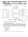
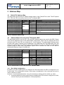
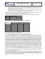
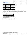
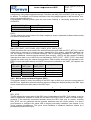
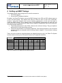
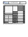
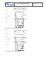
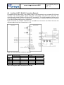
USER’S GUIDE
®
MICRO-LINE BUSMASTER BSP
Date
: 12 April 2006
Doc. no. : C641xCPU_ml_bm_ug
Iss./Rev : 1.0
Page
: 10
Figure 2: micro-line® peripheral interface
Figure 2 gives an overview of the available signals and their direction. For a detailed description of
the individual signals, please refer to chapter 6.
The C641xCPU allows different timings and different bus widths for EMIF CE2 and EMIF CE3
address spaces of the TMS320C641x DSP which reflect the chip select lines /CS1…/CS3 and
/CS4…/CS7 of the micro-line® peripheral interface. Therefore the bus access timing to connected
peripheral devices can be individually optimized within these two CE spaces without affecting other
components connected to other CE spaces. The timings for external micro-line® peripheral
interface accesses are based on the processor's external memory interface clock (EMIF clock).
which is 100 MHz by default. Several speed settings can be performed using the TMS320C641x
control registers for EMIF CE2 and EMIF CE3 address spaces which allow a wide range of microline® peripheral interface timings. The possible EMIF settings are shown in the table below.
EMIF Setting
Write Setup Time
Write Strobe Time
Write Hold Time
Read Setup Time
Read Strobe Time
Read Hold Time
Allowed range
1 to 15 clocks
1 to 63 clocks
0 to 3 clocks
1 to 15 clocks
1 to 63 clocks
0 to 7 clocks
Description
Address is valid and chip is enabled before write strobe is asserted
Write strobe is active
Address is valid and chip is enabled after write strobe is de-asserted
Address is valid and chip is enabled before read strobe is asserted
Time read strobe is active
Address is valid and chip is enabled after read strobe is de-asserted
Table 1: Supported EMIF Settings for CE2 and CE3 address spaces
The best values for micro-line® peripheral interface timings depend on:
• the minimum timing requirements for the FPGA