1
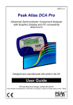
The Peak Atlas
Component Analyser
User Guide
Peak Electronic Design Limited is committed to continued product development and improvement. The
information and specifications contained within this user guide may therefore be subject to change.
Copyright Peak Electronic Design Limited 2000
Peak Atlas User Guide
July 2001, Rev. 5
Section
Page
Introduction .............................................................................. 3
Analysing components ............................................................. 4
Diodes ................................................................................ 5
Diode Networks ................................................................. 6
LEDs (including Bicolour LEDs)...................................... 7
Bipolar Junction Transistors (BJTs) .................................. 8
Enhancement Mode MOSFETs....................................... 11
Depletion Mode MOSFETs............................................. 12
Junction FETs .................................................................. 13
Thyristors (SCRs) and Triacs .......................................... 14
Care of your Atlas................................................................... 15
Technical Specifications......................................................... 16
Page 2
ENGLISH
Contents
Peak Atlas User Guide
July 2001, Rev. 5
The Peak Atlas is a new generation of intelligent component analyser that offers unrivalled
functionality together with refreshing simplicity. The Atlas brings a world of component data
to your fingertips.
Features
•
•
•
•
•
•
•
•
Automatic component identification.
Bipolar transistors
Darlington transistors
Enhancement Mode MOSFETs
Depletion Mode MOSFETs
Junction FETs
Triacs
Thyristors
LEDs
Bicolour LEDs
Diodes
Diode networks
Automatic pinout identification for all the above component types.
Special feature identification such as diode protection and resistor shunts.
Gain measurement for transistors.
Gate threshold measurement for Enhancement Mode MOSFETs.
Semiconductor forward voltage measure ments for diodes, LEDs and
transistors.
Semiconductor test current measurement.
Automatic and manual power-off.
The Peak Atlas is optimised to accurately analyse the vast majority of supported component
types. However, it is not possible to support every component due to the wide range of
required operating conditions, as such, displayed information should be interpreted
accordingly. Specification limits and specific analysis capabilities are detailed in this guide.
WARNING
Under no circumstances must the Atlas be connected to any powered devices as this may
cause damage to both the Atlas and the device under test. Additionally, the Atlas is not
rated for high voltage use and personal injury or death may result from inappropriate use.
Please note also that energy stored in external equipment’s capacitors may be sufficient to
cause irreparable damage to the Atlas. Analysis of discrete, unconnected components is
recommended.
Page 3
ENGLISH
Introduction
Peak Atlas User Guide
July 2001, Rev. 5
The Peak Atlas is designed to analyse discrete, unconnected, unpowered components. This
ensures that external connections don’t influence the measured parameters. The three test
probes can be connected to the component any way round. If the component has only two
terminals, then any pair of the three test probes can be used.
The Peak Atlas will start component analysis when the on/test button is pressed if the unit is
powered down. If the Atlas is not powered down
then a new analysis can be started by pressing and
The Peak Atlas
holding the scroll/off button first to power down
is analysing....
the unit and then pressing the on/test button.
Depending on the component type, analysis may take a few seconds to complete, after which,
the results of the analysis are displayed. Information is displayed a “page” at a time, each
page can be displayed by pressing the scroll/off button.
The arrow symbol on the display indicates that more pages are available to be viewed.
If the Atlas cannot detect any component between
any of the test probes, the following message will
be displayed:
No component
detected
If the component is not a supported component
type, a faulty component or a component that is
being tested in-circuit, the analysis may result in
the following message being displayed:
Unknown/Faulty
component
It is possible that the Atlas may detect one or more diode junctions or other
component type within an unknown or faulty part. This is because many
semiconductors comprise of pn (diode) junctions. Please refer to the section on
diodes and diode networks for more information.
Page 4
ENGLISH
Analysing Components
Peak Atlas User Guide
July 2001, Rev. 5
The Atlas will analyse almost any type of diode.
Any pair of the three test clips can be connected to
the diode, anyway round. If the Atlas detects a
single diode, the following message will be
displayed.
Pressing the scroll/off button will then display the
pinout for the diode. In this example, the Anode of
the diode is connected to the Red test clip and the
Cathode is connected to the Green test clip,
additionally, the Blue test clip is unconnected. The
forward voltage drop is then displayed, this gives
an indication of the diode technology. In this
example, it is likely that the diode is a silicon
diode. A germanium or Schottky diode may yield a
forward voltage of about 0.25V. The current at
which the diode was tested is also displayed.
Diode or diode
junction(s)
RED GREEN BLUE
Anod Cath
Forward voltage
Vf=0.67V
Test current
If=4.62mA
Note that the Atlas will detect only one diode even if two diodes are
connected in series when the third test clip is not connected to the junction
between the diodes. The forward voltage drop displayed however will be the
voltage across the whole series combination.
The Atlas will determine that the diode(s) under test is an LED if the
measured forward voltage drop exceeds 1.50V. Please refer to the section on
LED analysis for more information.
Zener diodes are not directly supported by the Atlas. Zener diodes with breakdown voltages
of approximately 5V or higher however, will be detected as a single diode.
Page 5
ENGLISH
Diodes
Peak Atlas User Guide
July 2001, Rev. 5
The Atlas will intelligently identify popular types of three terminal diode networks. For three
terminal devices such as SOT-23 diode networks, the three test clips must all be connected,
anyway round. The Atlas will identify the type of diode network and then display information
regarding each detected diode in sequence. The following types of diode networks are
automatically recognised by the Atlas:
Common cathode
diode network
Two-diode device with both cathodes connected
together, such as the Philips SOT-23 BAV70.
Common anode
diode network
Two-diode device with both anodes connected
together, such as the Philips SOT-323
BAW56W.
Series
diode network
Two-diode device with each diode connected in
series. The Philips SOT-23 BAV99 is a popular
type of series diode network.
Following the component identification page, the
Atlas will display details of each detected diode
within the diode network.
Firstly, the pinout for the diode is displayed,
followed by the electrical information, forward
voltage drop and the current at which the diode
was tested. The value of the test current depends
on the measured forward voltage drop of the
diode.
Following the display of all the details for the first
diode, the details of the second diode will then be
displayed.
Page 6
Pinout for D1...
RED GREEN BLUE
Anod Cath
Forward voltage
D1 Vf=0.67V
Test current
D1 If=4.62mA
ENGLISH
Diode Networks
Peak Atlas User Guide
July 2001, Rev. 5
An LED is really just a another type of diode,
LED or diode
however, the Atlas will determine that an LED or
LED network has been detected if the measured
junction(s)
forward voltage drop is larger than 1.5V. This
also enables the Atlas to intelligently identify bicolour LEDs, both two-terminal and threeterminal varieties.
RED GREEN BLUE
Cath Anod
Like the diode analysis, the pinout, the forward
voltage drop and the associated test current is
displayed.
Forward voltage
Vf=1.92V
Here, the Cathode (-ve) LED terminal is connected
to the Green test clip and the Anode (+ve) LED
terminal is connected to the Blue test clip.
Test current
If=3.28mA
In this example, a simple green LED yields a
forward voltage drop of 1.92V at the test current of
3.28mA. The test current depends on the forward
voltage.
Bicolour LEDs
Bicolour LEDs are automatically identified. A
Two terminal
two terminal bicolour LED consists of two LED
chips which are connected in inverse parallel
bicolour LED
within the LED body. Three terminal bicolour
LEDs are made with either common anodes or
common cathodes. The pinouts and the electrical
Three terminal
characteristics are displayed in the same way as
bicolour LED
the diode networks analysis. The details of each
LED
chip
are
individually
displayed.
Interestingly, this allows for the pinouts relating to the different colours within the bicolour
LED to be determined. This is because, different colour LEDs exhibit different forward
voltage drops. Red LEDs often have the lowest forward voltage drop, followed by yellow
LEDs, green LEDs and finally, blue LEDs.
Some blue LEDs (and their cousins, white phosphor LEDs) require high
forward voltages and may not be detected by the Atlas.
Page 7
ENGLISH
LEDs (including bicolour LEDs)
Peak Atlas User Guide
July 2001, Rev. 5
Bipolar Junction Transistors (BJTs)
ENGLISH
Bipolar Junction Transistors are simply “conventional” transistors,
although variants of these do exist such as Darlingtons, diode protected,
resistor shunted types and combinations of these types. All of these
variations are automatically identified by the Atlas.
Bipolar Junction Transistors are available in two
main types, NPN and PNP. In this example, the
Atlas has detected an PNP transistor.
PNP bipolar
transistor
If an NPN Darlington transistor
was detected for example, the
following message would be
displayed:
NPN bipolar
Darlington
Please note that the Atlas will determine that the transistor under test is a Darlington
type if the base-emitter voltage drop is greater than 1.00V for devices with a base-emitter
shunt resistance of greater than 60kΩ or if the base-emitter voltage drop is greater than
0.80V for devices with a base-emitter shunt resistance of less than 60kΩ. The measured
base-emitter voltage drop is displayed as detailed later in this section.
Pressing the scroll/off button will result in the
transistor’s pinout being displayed. Here, the Atlas
has identified that the Base is connected to the Red
test clip, the Collector is connected to the Green
test clip and the Emitter is connected to the Blue
test clip.
RED GREEN BLUE
Base Coll Emit
C
Faulty or Very Low Gain Transistors
B
Faulty transistors that exhibit no or very low gain may cause the
Atlas to only identify one or more diode junctions within the
E
device. This is because NPN transistors consist of a structure of
junctions that behave like a common anode diode
network. PNP transistors can appear to be common
cathode diode networks. The common junction
Common anode
represents the base terminal. This is normal for
diode network
situations where the current gain is so low that it is
immeasurable at the test currents used by the Atlas.
Page 8
Peak Atlas User Guide
July 2001, Rev. 5
Many modern transistors contain additional special features. If the Atlas has detected any
special features, then the details of these features are displayed next after pressing the
scroll/off button.
Some transistors, particularly CRT
Diode protection
deflection transistors and many
large
Darlingtons
have
a
between C-E
protection diode inside their
package connected between the
collector and emitter. The Philips BU505DF is a typical example of a diode
protected bipolar transistor. Remember that protection diodes are always internally connected
between the collector and the emitter so that they are normally reverse biased. For NPN
transistors, the anode of the diode is connected to the emitter of the transistor. For PNP
transistors, the anode of the diode is connected to the collector of the transistor.
Additionally, many Darlingtons and a few conventional transistors also have a resistor shunt
network between the base and emitter of the device. The Atlas can detect the resistor shunt if
it has a resistance of typically less than 60kΩ. The popular Motorola TIP110 Darlington
transistor contains internal resistors between the base and emitter.
Resistor shunt
between B-E
HFE not accurate
due to B-E res
It is important to note that if a transistor does contain a base-emitter shunt
resistor network, any measurements of current gain (HFE) will be very low at
the test currents used by the Atlas. This is due to the resistors providing an
additional path for the base current. The readings for gain however can still be
used for comparing transistors of a similar type for the purposes of matching or
gain band selecting. The Atlas will warn you if such a condition arises as
illustrated above.
Page 9
ENGLISH
Transistor Special Features
Peak Atlas User Guide
July 2001, Rev. 5
Current gain
HFE=126
The DC current gain (HFE) is displayed after any
special transistor features that may have been
displayed.
DC current gain is simply the ratio of the collector
current to the base current for a particular operating
condition. The Atlas measures HFE at a collector
current of 2.50mA and a collector-emitter voltage
of between 2V and 3V. The gain of all transistors
can vary considerably with collector current, collector voltage and also temperature. The
displayed value for gain therefore may not represent the gain experienced at other collector
currents and voltages. This is particularly true for large devices.
Test current
Ic=2.50mA
Darlington transistors can have very high gain values and more variation of gain will be
evident as a result of this.
Additionally, it is quite normal for transistors of the same type to have a wide range of gain
values. For this reason, transistor circuits are often designed so that their operation has little
dependence on the absolute value of current gain.
The displayed value of gain is very useful however for comparing transistors of a similar type
for the purposes of gain matching or fault finding.
Base-Emitter Voltage Drop
Finally, the DC characteristics of the base-emitter
junction are displayed, both the base-emitter
forward voltage drop and the base current used for
the measurement.
B-E voltage
Vbe=0.77V
The forward base-emitter voltage drop can aid in
Test current
the identification of silicon or germanium devices.
Germanium devices can have base-emitter voltages
Ib=4.52mA
as low as 0.2V, Silicon types exhibit readings of
about 0.7V and Darlington transistors can exhibit readings of about 1.2V because of the
multiple base-emitter junctions being measured.
Note that the Atlas does not perform the base-emitter tests at the same base current as that
used for the current gain measurement.
Page 10
ENGLISH
Current Gain (HFE)
Peak Atlas User Guide
July 2001, Rev. 5
MOSFET stands for Metal Oxide Semiconductor Field Effect Transistor.
Like bipolar transistors, MOSFETs are available in two main types, NChannel and P-Channel. Most modern MOSFETs are of the Enhancement
Mode type, meaning that the bias of the gate-source voltage is always
positive (For N-Channel types). The other (rarer) type of MOSFET is the
Depletion Mode type which is described in a later section.
MOSFETs of all types are sometimes known as IGFETs, meaning Insulated Gate Field Effect
Transistor. This term describes a key feature of these devices, an insulated gate region that
results in negligible gate current for both positive
and negative gate-source voltages (up to the
Enhancement mode
maximum allowed values of course, typically
N-Ch MOSFET
±20V).
The first screen to be displayed gives information
on the type of MOSFET detected. Pressing
scroll/off will then result in the pinout of the
MOSFET being displayed. The gate, source and
drain are each identified.
An important feature of a MOSFET is the gatesource threshold voltage, the gate-source voltage
at which conduction between the source and
drain starts. The gate threshold is displayed
following the pinout information.
The Atlas detects that drain-source conduction
has started when it reaches 2.50mA. This
condition is confirmed by the next displayed
page.
RED GREEN BLUE
Gate Drn Srce
Gate Threshold
Vgs=3.47V
Test current
Id=2.50mA
All Enhancement Mode MOSFETs contain a protection diode junction
between the source and drain terminals. If the Atlas does not detect this diode
the device will be rejected as an Enhancement Mode MOSFET.
Page 11
ENGLISH
Enhancement mode MOSFETs
Peak Atlas User Guide
July 2001, Rev. 5
The rare Depletion Mode MOSFET is very similar to the conventional
Junction FET (JFET) except that the gate terminal is insulated from the
other two terminals. The input resistance of these devices can typically be
greater than 1000MΩ for negative and positive gate-source voltages.
Depletion Mode devices are characterised by the
gate-source voltage required to control the drainsource current. Modern Depletion Mode devices
are generally only available in N-Channel varieties
and will conduct current between it’s drain and
source terminals even with a zero voltage applied across the gate and the source. The device
can only be turned completely off by taking it’s gate significantly more negative than it’s
source terminal, say –10V. It is this characteristic that makes them so similar to conventional
JFETs.
Depletion mode
N-Ch MOSFET
Pressing scroll/off will cause the pinout screen to
be displayed.
Page 12
RED GREEN BLUE
Drn Gate Srce
ENGLISH
Depletion Mode MOSFETs
Peak Atlas User Guide
July 2001, Rev. 5
Junction FETs are conventional Field Effect Transistors.
The voltage applied across the gate-source terminals controls current
between the drain and source terminals. N-Channel JFETs require a
negative voltage on their gate with respect to their source, the more
negative the voltage, the less current can flow between the drain and source.
Unlike Depletion Mode MOSFETs, JFETs have no insulation layer on the gate. This means
that although the input resistance between the gate and source is normally extremely high
(greater than 100MΩ), the gate current can rise if the semiconductor junction between the
gate and source or between the gate and drain become forward biased. This can happen if the
gate voltage becomes about 0.6V higher than either the drain or source terminals for NChannel devices or 0.6V lower than the drain or source for P-Channel devices.
The internal structure of JFETs is essentially
symmetrical about the gate terminal, this means
that the drain and source terminals are
indistinguishable by the Atlas. The JFET type and
the gate terminal are identified however.
Drain and Source
not identified
P-Channel
Junction FET
RED GREEN BLUE
Gate
Page 13
ENGLISH
Junction FETs (JFETs)
Peak Atlas User Guide
July 2001, Rev. 5
Sensitive low power thyristors (Silicon Controlled Rectifiers
- SCRs) and triacs can be easily identified and analysed with
the Atlas. Triac operation is very similar to that of thyristors,
although the Atlas is able to distinguish between
them.
Sensitive
Thyristor terminals are the anode, cathode and the
gate. The pinout of the thyristor under test will be
displayed on the next press of the scroll/off button.
Sensitive or low
power triac
RED GREEN BLUE
MT1 MT2 Gate
or low
power thyristor
RED GREEN BLUE
Gate Anod Cath
Triac terminal nomenclature is less universal than
most components although many manufacturers are
standardising on the terms gate, MT1 and MT2,
(MT standing for main terminal). To avoid
ambiguity, MT1 is the terminal with which gate
current is referenced. That is, gate current is
injected or extracted from the gate-MT1 junction.
The Atlas determines that the device under test is a triac by checking the
gate trigger quadrants that the device will reliably operate in. Thyristors operate
in only one quadrant (positive gate current, positive anode current). Triacs can
typically operate in three or four quadrants, hence their use in AC control
applications.
The test currents used by the Atlas are kept low (<5mA) to eliminate the
possibility of damage to a vast range of component types. Some thyristors and
triacs will not operate at low currents and these types cannot be analysed with
this instrument. Note also that if only one trigger quadrant of a triac is detected
then the Atlas will conclude that it has found a thyristor. Please see the
technical specifications for more details.
Page 14
ENGLISH
Thyristors (SCRs) and Triacs
Peak Atlas User Guide
July 2001, Rev. 5
The Peak Atlas should provide many years of service if used in accordance with this user
guide. Care should be taken not to expose your unit to excessive heat, shock or moisture.
Additionally, the battery should be replaced at least every 12 months to reduce the risk of leak
damage.
If a low battery warning message appears,
immediate replacement of the battery is
recommended as measured parameters may be
affected. The Atlas will however continue to
operate.
* Low Battery *
The battery can be replaced by carefully opening the Atlas by removing the three screws from
the rear of the unit. Take care not to damage the electronics.
The battery should only be replaced with a high quality battery identical to, or equivalent to
an Alkaline GP23A or MN21 12V (10mm diameter x 28mm length). Replacement batteries
are available directly from Peak Electronic Design Limited.
Self Test Procedure
Each time the Atlas is powered up, a self test procedure is performed. In addition to a battery
voltage test, the Atlas measures the performance of many internal functions such as the
voltage and current sources, amplifiers, analogue to
digital converters and test lead multiplexers. If any
Self test failed
of these function measurements fall outside tight
performance limits, a message will be displayed
CODE: 5
and the Atlas will switch off automatically.
If the problem was caused by a temporary condition on the test clips, such as applying power
to the test clips, then simply re-starting the Atlas may clear the problem.
If a persistent problem does arise, it is likely that damage has been caused by an external
event such as excessive power being applied to the test clips or a large static discharge taking
place. If the problem persists, please contact us for further advice, quoting the displayed fault
code.
If there is a low battery condition, the automatic self test procedure will
not be performed.
Page 15
ENGLISH
Care of your Atlas
Peak Atlas User Guide
July 2001, Rev. 5
Technical Specifications
Parameter
Peak test current into S/C
Peak test voltage across O/C
Measurable transistor gain range (HFE)
Transistor gain accuracy
Transistor VCEO
Transistor VBE accuracy
VBE for Darlington identification
VBE for Darlington identification (shunted)
Acceptable transistor VBE
Base-emitter shunt resistance threshold
Transistor collector-emitter test current
Acceptable transistor collector leakage
EM MOSFET gate threshold range
EM MOSFET gate threshold accuracy
EM MOSFET drain-source test current
EM MOSFET minimum gate resistance
DM MOSFET drain-source test current
JFET drain-source test current
Thyristor/Triac gate test current
Thyristor/Triac load test current
Diode test current
Diode forward voltage accuracy
VF for LED identification
Battery type
Battery voltage range
Battery voltage warning threshold
Inactivity power-down period
Dimensions (excluding test leads)
Operating temperature range
1.
2.
3.
4.
5.
6.
7.
8.
9.
Minimum
-5.5mA
-5.1V
4
Typical
Maximum
5.5mA
5.1V
65000
±3% ±5 HFE
2.0V
-2%-20mV
3.0V
+2%+20mV
1.0V
0.8V
Note
1
1
2
2,9
2
9
3
4
1.80V
2.45mA
0.1V
-2%-20mV
2.45mA
60kΩ
2.50mA
0.7mA
2.50mA
8kΩ
0.5mA
0.5mA
2.55mA
5.0V
+2%+20mV
2.55mA
6
5
5
5.5mA
5.5mA
4.5mA
5.0mA
5.0mA
-2%-20mV
+2%+20mV
1.50V
GP23A 12V Alkaline
7.50V
12V
8.25V
30 secs (5 secs for single screen results)
103 x 70 x 20 mm
0°C
50°C
7
8
Between any pair of test clips.
Collector current of 2.50mA. Gain accuracy valid for gains less than 2000.
Resistance across reverse biased base-emitter > 60kΩ.
Resistance across reverse biased base-emitter < 60kΩ.
Drain-source current of 2.50mA.
Collector-emitter voltage of 5.0V.
Thyristor quadrant I, Triac quadrants I and III.
Subject to acceptable LCD visibility.
BJT with no shunt resistors.
Designed and made in England by Peak Electronic Design Limited
Alas House, Kiln Lane, Harpur Hill Industrial Estate, Buxton, Derbyshire, SK17 9JL, England.
Web: www.peakelec.co.uk Email: [email protected]
Telephone. +44 (0) 1298 70012 Fax: +44 (0) 1298 70046
Page 16
ENGLISH
All values are at 25°C unless otherwise specified.