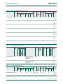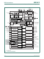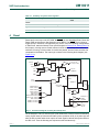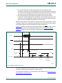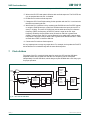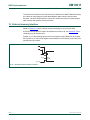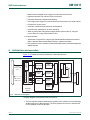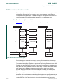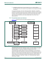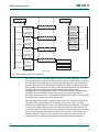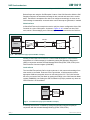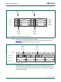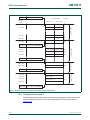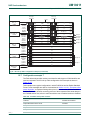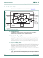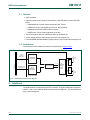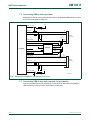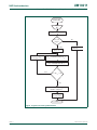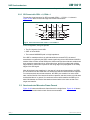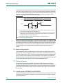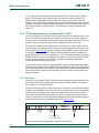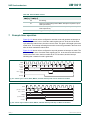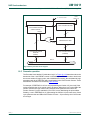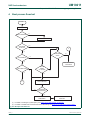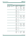
1
UM10211
LPC23XX User manual
Rev. 01 — 11 March 2008
User manual
Document information
Info
Content
Keywords
LPC2300, LPC2364, LPC2365, LPC2366, LPC2367, LPC2368, LPC2377,
LPC2378, LPC2387, LPC2388, ARM, ARM7, 32-bit, USB, Ethernet, CAN,
I2S, Microcontroller
Abstract
An initial LPC2364/65/66/67/68/77/78/87/88 User manual revision
UM10211
NXP Semiconductors
LPC23XX User manual
Revision history
Rev
Date
Description
01
20080311
LPC2364/65/66/67/68/77/78/87/88 User manual
Contact information
For more information, please visit: http://www.nxp.com
For sales office addresses, please send an email to: [email protected]
UM10211_1
User manual
© NXP B.V. 2008. All rights reserved.
Rev. 01 — 11 March 2008
2 of 684
UM10211
Chapter 1: LPC23XX Introductory information
Rev. 01 — 11 March 2008
User manual
1. Introduction
LPC23xx series are ARM-based microcontrollers for applications requiring serial
communications for a variety of purposes. These microcontrollers typically incorporate a
10/100 Ethernet MAC, USB 2.0 Full Speed interface, four UARTs, two CAN channels, an
SPI interface, two Synchronous Serial Ports (SSP), three I2C interfaces, an I2S interface,
and a MiniBus (8-bit data/16-bit address parallel bus).
2. How to read this manual
The term “LPC23xx“ in the following text will be used as a generic name for all parts
covered in this user manual:
•
•
•
•
LPC2364/65/66/67/68
LPC2377/78
LPC2387
LPC2388
Only when needed, a specific device name will be used to distinguish the part. See
Table 1–1 to find information about a particular part.
Table 1.
LPC23xx overview
Part
Features
Ordering info
Ordering options Block diagram
LPC2364/65/66/67/68
Section 1–3.1
Table 1–3
Table 1–4
Figure 1–1
LPC2377/78
Section 1–3.1, Table 1–3
Section 1–3.2
Table 1–5
Figure 1–2
LPC2387
Section 1–3.1, Table 1–3
Section 1–3.3
Table 1–6
Figure 1–3
LPC2388
Section 1–3.1, Table 1–3
Section 1–3.3
Table 1–7
Figure 1–4
3. Features
3.1 General features
• ARM7TDMI-S processor, running at up to 72 MHz.
• Up to 512 kB on-chip Flash Program Memory with In-System Programming (ISP) and
In-Application Programming (IAP) capabilities. Single Flash sector or full-chip erase in
400 ms and 256 bytes programming in 1 ms. Flash program memory is on the ARM
local bus for high performance CPU access.
• Up to 64 kB of SRAM on the ARM local bus for high performance CPU access.
• 16 kB Static RAM for Ethernet interface. Can also be used as general purpose SRAM.
• 8 kB Static RAM for general purpose or USB interface.
UM10211_1
User manual
© NXP B.V. 2008. All rights reserved.
Rev. 01 — 11 March 2008
3 of 684
UM10211
NXP Semiconductors
Chapter 1: LPC23XX Introductory information
• Dual AHB system that provides for simultaneous Ethernet DMA, USB DMA, and
program execution from on-chip flash with no contention between those functions. A
bus bridge allows the Ethernet DMA to access the other AHB subsystem.
• Advanced Vectored Interrupt Controller, supporting up to 32 vectored interrupts.
• General Purpose DMA controller (GPDMA) on AHB that can be used with the SSP
serial interfaces, the I2S port, and the SD/MMC card port, as well as for
memory-to-memory transfers.
• Serial Interfaces:
– Ethernet MAC with associated DMA controller. These functions reside on an
independent AHB bus.
– On LPC2364/66/68, LPC2378, LPC2387, LPC2388: USB 2.0 device controller
with on-chip PHY and associated DMA controller.
– On LPC2388: USB Host/OTG controller.
– Four UARTs with fractional baud rate generation, one with modem control I/O, one
with IrDA support, all with FIFO. These reside on the APB bus.
– SPI controller, residing on the APB bus.
– Two SSP controllers with FIFO and multi-protocol capabilities. One is an alternate
for the SPI port, sharing its interrupt. The SSP controllers can be used with the
GPDMA controller and reside on the APB bus.
– Three I2C interfaces reside on the APB bus. The second and third I2C interfaces
are expansion I2C interfaces with standard port pins rather than special open-drain
I2C pins.
– I2S (Inter-IC Sound) interface for digital audio input or output, residing on the APB
bus. The I2S interface can be used with the GPDMA.
– On LPC2364/66/68, LPC2378, LPC2387, LPC2388: Two CAN channels with
Acceptance Filter/FullCAN mode residing on the APB bus.
• Other APB Peripherals:
– On LPC2367/68, LPC2377/78, LPC2387, LPC2388: Secure Digital (SD) /
MultiMediaCard (MMC) memory card interface.
– Up to 70 (100 pin packages) or 104 (144 pin packages) general purpose I/O pins.
– 10 bit A/D converter with input multiplexing among 6 pins (100 pin packages) or 8
pins (144 pin packages).
– 10 bit D/A converter.
– Four general purpose timers with two capture inputs each and up to four compare
output pins each. Each timer block has an external count input.
– One PWM/Timer block with support for three-phase motor control. The PWM has
two external count inputs.
– Real-Time Clock (RTC) with separate power pin; clock source can be the RTC
oscillator or the APB clock.
– 2 kB Static RAM powered from the RTC power pin, allowing data to be stored
when the rest of the chip is powered off.
– Watchdog Timer. The watchdog timer can be clocked from the internal RC
oscillator, the RTC oscillator, or the APB clock.
• Standard ARM Test/Debug interface for compatibility with existing tools.
UM10211_1
User manual
© NXP B.V. 2008. All rights reserved.
Rev. 01 — 11 March 2008
4 of 684
UM10211
NXP Semiconductors
Chapter 1: LPC23XX Introductory information
•
•
•
•
•
Emulation Trace Module.
Support for real-time trace.
Single 3.3 V power supply (3.0 V to 3.6 V).
Three reduced power modes: Idle, Sleep, and Power-down.
Four external interrupt inputs. In addition every PORT0/2 pin can be configured as an
edge sensing interrupt.
• Processor wakeup from Power-down mode via any interrupt able to operate during
Power-down mode (includes external interrupts, RTC interrupt, and Ethernet wakeup
interrupt).
• Two independent power domains allow fine tuning of power consumption based on
needed features.
•
•
•
•
Brownout detect with separate thresholds for interrupt and forced reset.
On-chip Power On Reset.
On-chip crystal oscillator with an operating range of 1 MHz to 24 MHz.
4 MHz internal RC oscillator that can optionally be used as the system clock. For USB
and CAN application, the use of an external clock source is suggested.
• On-chip PLL allows CPU operation up to the maximum CPU rate without the need for
a high-frequency crystal. May be run from the main oscillator, the internal RC
oscillator, or the RTC oscillator.
• Boundary scan for simplified board testing is available in LPC2364FET100,
LPC2368FET100 (TFBGA packages), LPC2377/78, and LPC2388.
• Versatile pin function selections allow more possibilities for using on-chip peripheral
functions.
3.2 Features available in LPC2377/78 and LPC2388
External memory controller that supports static devices such as Flash and SRAM. An 8-bit
data/16-bit address parallel bus is available.
3.3 Features available in LPC2387 and LPC2388
• 64 kB of SRAM on the ARM local bus for high performance CPU access.
• 16 kB Static RAM for USB interface. Can also be used as general purpose SRAM.
3.4 Overview
The following table shows the differences between LPC23xx parts. Features that are the
same for all parts are not included.
Table 2.
LPC23xx features overview
Part
SRAM/
kB
Flash/
kB
EMC
USB/GP
SRAM/
kB
USB
device
USB
host/
OTG
CAN
SD/MMC ADC
GPIO
channels
channels pins
LPC2364 8
128
no
8
yes
no
2
no
6
70
LPC2365 32
256
no
8
no
no
-
no
6
70
LPC2366 32
256
no
8
yes
no
2
no
6
70
LPC2367 32
512
no
8
no
no
-
yes
6
70
UM10211_1
User manual
© NXP B.V. 2008. All rights reserved.
Rev. 01 — 11 March 2008
5 of 684
UM10211
NXP Semiconductors
Chapter 1: LPC23XX Introductory information
Table 2.
LPC23xx features overview
Part
SRAM/
kB
Flash/
kB
EMC
USB/GP
SRAM/
kB
USB
device
USB
host/
OTG
CAN
SD/MMC ADC
GPIO
channels
channels pins
LPC2368 32
512
no
8
yes
no
2
yes
6
70
LPC2377 32
512
Mini
8
no
no
-
yes
8
104
LPC2378 32
512
Mini
8
yes
no
2
yes
8
104
LPC2387 64
512
no
16
yes
no
2
yes
6
70
LPC2388 64
512
Mini
16
yes
yes
2
yes
8
104
4. Applications
• Industrial control
• Medical systems
5. Ordering information and options
For ordering information for all LPC23xx parts, see Table 1–3. For ordering options, see
•
•
•
•
Table 3.
Table 1–4 for LPC2364/65/66/67/68 parts.
Table 1–5 for LPC2377/78.
Table 1–6 for LPC2387.
Table 1–7 for LPC2388.
LPC23xx ordering information
Type number
Package
Name
Description
Version
LPC2364FBD100
LQFP100
plastic low profile quad flat package; 100 leads; body 14 × 14 × 1.4 mm
SOT407-1
LPC2364FET100
TFBGA100
plastic thin fine-pitch ball grid array package; 100 balls; body 9 × 9 × 0.7 mm SOT926-1
LPC2365FBD100
LQFP100
plastic low profile quad flat package; 100 leads; body 14 × 14 × 1.4 mm
SOT407-1
LPC2366FBD100
LQFP100
plastic low profile quad flat package; 100 leads; body 14 × 14 × 1.4 mm
SOT407-1
LPC2367FBD100
LQFP100
plastic low profile quad flat package; 100 leads; body 14 × 14 × 1.4 mm
SOT407-1
LPC2368FBD100
LQFP100
plastic low profile quad flat package; 100 leads; body 14 × 14 × 1.4 mm
SOT407-1
LPC2368FET100
TFBGA100
plastic thin fine-pitch ball grid array package; 100 balls; body 9 × 9 × 0.7 mm SOT926-1
LPC2377FBD144
LQFP144
plastic low profile quad flat package; 144 leads; body 20 × 20 × 1.4 mm
SOT486-1
LPC2378FBD144
LQFP144
plastic low profile quad flat package; 144 leads; body 20 × 20 × 1.4 mm
SOT486-1
LPC2387FBD100
LQFP100
plastic low profile quad flat package; 100 leads; body 14 × 14 × 1.4 mm
SOT407-1
LPC2388FBD144
LQFP144
plastic low profile quad flat package; 144 leads; body 20 × 20 × 1.4 mm
SOT486-1
UM10211_1
User manual
© NXP B.V. 2008. All rights reserved.
Rev. 01 — 11 March 2008
6 of 684
UM10211
NXP Semiconductors
Chapter 1: LPC23XX Introductory information
Table 4.
LPC2364/65/66/67/68 Ordering options
Type number
Flash
(kB) Local
bus
SRAM (kB)
Ether USB
SD/ GP
Channels
Temp
net
device
MMC
DMA
Ethernet GP/ RTC Total
CAN ADC DAC range
+ 4 kB
buffers
USB
FIFO
LPC2364FBD100 128
8
16
8
2
34
RMII
yes
no
yes
2
6
1
−40 °C
to
+85 °C
LPC2364FET100 128
8
16
8
2
34
RMII
yes
no
yes
2
6
1
−40 °C
to
+85 °C
LPC2365FBD100 256
32
16
8
2
58
RMII
no
no
yes
-
6
1
−40 °C
to
+85 °C
LPC2366FBD100 256
32
16
8
2
58
RMII
yes
no
yes
2
6
1
−40 °C
to
+85 °C
LPC2367FBD100 512
32
16
8
2
58
RMII
no
yes
yes
-
6
1
−40 °C
to
+85 °C
LPC2368FBD100 512
32
16
8
2
58
RMII
yes
yes
yes
2
6
1
−40 °C
to
+85 °C
LPC2368FET100 512
32
16
8
2
58
RMII
yes
yes
yes
2
6
1
−40 °C
to
+85 °C
LPC2377/78 ordering options
USB
device
+ 4 kB
FIFO
SD/ GP
MMC DMA
Temp
range
32 16 8
2
58 MiniBus: 8 data, 16
address, and 2 chip
select lines
RMII
no
-
yes
yes
8
1
−40 °C to
+85 °C
LPC2378FBD144 512
32 16 8
2
58 MiniBus: 8 data, 16
address, and 2 chip
select lines
RMII
yes
2
yes
yes
8
1
−40 °C to
+85 °C
Table 6.
GP/USB
LPC2377FBD144 512
Local bus
DAC channels
Ether
net
ADC channels
External bus
CAN channels
SRAM (kB)
Total
Flash
(kB)
RTC
Type number
Ethernet buffer
Table 5.
LPC2387 ordering options
Type number
Flash
(kB) Local
bus
LPC2387FBD100 512
64
SRAM (kB)
Ether USB
SD/ GP
Channels
Temp
net
device
MMC
DMA
Ethernet GP/ RTC Total
CAN ADC DAC range
+
4
kB
buffers
USB
FIFO
16
16
2
98
RMII
UM10211_1
User manual
yes
yes
yes
2
6
1
−40 °C
to
+85 °C
© NXP B.V. 2008. All rights reserved.
Rev. 01 — 11 March 2008
7 of 684
UM10211
NXP Semiconductors
Chapter 1: LPC23XX Introductory information
LPC2388 ordering options
98 MiniBus: 8 data, 16 RMII
address, and 2 chip
select lines
USB
device
host
OTG+
4 kB
FIFO
yes
SD/ GP
MMC DMA
CAN channels
Total
Ether
net
2
yes
yes
Temp
range
DAC channels
64 16 16 2
External bus
ADC channels
LPC2388FBD144 512
RTC
SRAM (kB)
GP/USB
Flash
(kB)
Local bus
Type number
Ethernet buffer
Table 7.
8
1
−40 °C to
+85 °C
6. Architectural overview
The LPC2300 consists of an ARM7TDMI-S CPU with emulation support, the ARM7 Local
Bus for closely coupled, high speed access to the majority of on-chip memory, the AMBA
Advanced High-performance Bus (AHB) interfacing to high speed on-chip peripherals and
external memory, and the AMBA Advanced Peripheral Bus (APB) for connection to other
on-chip peripheral functions. The microcontroller permanently configures the
ARM7TDMI-S processor for little-endian byte order.
The microcontroller implements two AHB buses in order to allow the Ethernet block to
operate without interference caused by other system activity. The primary AHB, referred
to as AHB1, includes the Vectored Interrupt Controller, General Purpose DMA Controller,
External Memory Controller, USB interface, and 8/16 kB SRAM primarily intended for use
by the USB.
The second AHB, referred to as AHB2, includes only the Ethernet block and an
associated 16 kB SRAM. In addition, a bus bridge is provided that allows the secondary
AHB to be a bus master on AHB1, allowing expansion of Ethernet buffer space into
off-chip memory or unused space in memory residing on AHB1.
In summary, bus masters with access to AHB1 are the ARM7 itself, the USB block, the
General Purpose DMA function, and the Ethernet block (via the bus bridge from AHB2).
Bus masters with access to AHB2 are the ARM7 and the Ethernet block.
AHB peripherals are allocated a 2 MB range of addresses at the very top of the 4 GB
ARM memory space. Each AHB peripheral is allocated a 16 kB address space within the
AHB address space. Lower speed peripheral functions are connected to the APB bus.
The AHB to APB bridge interfaces the APB bus to the AHB bus. APB peripherals are also
allocated a 2 MB range of addresses, beginning at the 3.5 GB address point. Each APB
peripheral is allocated a 16 kB address space within the APB address space.
7. ARM7TDMI-S processor
The ARM7TDMI-S is a general purpose 32 bit microprocessor, which offers high
performance and very low power consumption. The ARM architecture is based on
Reduced Instruction Set Computer (RISC) principles, and the instruction set and related
decode mechanism are much simpler than those of microprogrammed Complex
Instruction Set Computers. This simplicity results in a high instruction throughput and
impressive real-time interrupt response from a small and cost-effective processor core.
UM10211_1
User manual
© NXP B.V. 2008. All rights reserved.
Rev. 01 — 11 March 2008
8 of 684
UM10211
NXP Semiconductors
Chapter 1: LPC23XX Introductory information
Pipeline techniques are employed so that all parts of the processing and memory systems
can operate continuously. Typically, while one instruction is being executed, its successor
is being decoded, and a third instruction is being fetched from memory.
The ARM7TDMI-S processor also employs a unique architectural strategy known as
THUMB, which makes it ideally suited to high-volume applications with memory
restrictions, or applications where code density is an issue.
The key idea behind THUMB is that of a super-reduced instruction set. Essentially, the
ARM7TDMI-S processor has two instruction sets:
• The standard 32 bit ARM instruction set.
• A 16 bit THUMB instruction set.
The THUMB set’s 16 bit instruction length allows it to approach twice the density of
standard ARM code while retaining most of the ARM’s performance advantage over a
traditional 16 bit processor using 16 bit registers. This is possible because THUMB code
operates on the same 32 bit register set as ARM code.
THUMB code is able to provide up to 65% of the code size of ARM, and 160% of the
performance of an equivalent ARM processor connected to a 16 bit memory system.
The ARM7TDMI-S processor is described in detail in the ARM7TDMI-S Datasheet that
can be found on official ARM website.
8. On-chip flash memory system
The LPC2300 includes a Flash memory system with up to 512 kB. This memory may be
used for both code and data storage. Programming of the Flash memory may be
accomplished in several ways. It may be programmed In System via the serial port. The
application program may also erase and/or program the Flash while the application is
running, allowing a great degree of flexibility for data storage field firmware upgrades, etc.
The Flash is 128 bits wide and includes pre-fetching and buffering techniques to allow it to
operate at SRAM speeds.
9. On-chip Static RAM
The LPC2300 includes a static RAM memory up to 64 kB in size, that may be used for
code and/or data storage.
The SRAM controller incorporates a write-back buffer in order to prevent CPU stalls
during back-to-back writes. The write-back buffer always holds the last data sent by
software to the SRAM. The data is only written to the SRAM when software does another
write. After a "warm" chip reset, the SRAM does not reflect the last write operation. Two
identical writes to a location guarantee that the data will be present after a Reset.
Alternatively, a dummy write operation before entering idle or power-down mode will
similarly guarantee that the last data written will be present after a subsequent Reset.
UM10211_1
User manual
© NXP B.V. 2008. All rights reserved.
Rev. 01 — 11 March 2008
9 of 684
UM10211
NXP Semiconductors
Chapter 1: LPC23XX Introductory information
10. Block diagram
TMS TDI
XTAL1
XTAL2
VDDA
trace signals
LPC2364/65/66/67/68
P0, P1, P2,
P3, P4
8/32 kB
SRAM
HIGH-SPEED
GPI/O
70 PINS
TOTAL
128/256/
512 kB
FLASH
INTERNAL
CONTROLLERS
EINT3 to EINT0
P0, P2
ARM7TDMI-S
SRAM FLASH
AHB2
RMII(8)
TEST/DEBUG
INTERFACE
ETHERNET
MAC WITH
DMA
EMULATION
TRACE MODULE
TRST TCK TDO
EXTIN0
RESET
PLL
SYSTEM
FUNCTIONS
system
clock
INTERNAL RC
OSCILLATOR
AHB1
AHB
BRIDGE
MASTER AHB TO SLAVE
PORT AHB BRIDGE PORT
AHB TO
APB BRIDGE
8 kB
SRAM
USB WITH
4 kB RAM
AND DMA(2)
I2SRX_CLK
I2STX_CLK
I2SRX_WS
I2STX_WS
I2SRX_SDA
I2STX_SDA
I2S INTERFACE
CAPTURE/COMPARE
TIMER0/TIMER1/
TIMER2/TIMER3
6 × PWM1
PWM1
SPI, SSP0 INTERFACE
LEGACY GPI/O
52 PINS TOTAL
SSP1 INTERFACE
2 × PCAP1
P0, P1
6 × AD0
A/D CONVERTER
AOUT
SCK1
MOSI1
MISO1
SSEL1
MCICMD,
MCIDAT[3:0]
UART0, UART2, UART3
TXD0, TXD2, TXD3
RXD0, RXD2, RXD3
2 kB BATTERY RAM
TXD1
RXD1
DTR1, RTS1
power domain
domain 22
power
RTCX1
RTCX2
SCK, SCK0
MOSI, MOSI0
MISO, MISO0
SSEL, SSEL0
MCICLK, MCIPWR
SD/MMC CARD
INTERFACE(1)
D/A CONVERTER
VBAT
VBUS
USB_D+, USB_D−
USB_CONNECT
USB_UP_LED
GP DMA
CONTROLLER
EXTERNAL INTERRUPTS
2 × CAP0/CAP1/
CAP2/CAP3
4 × MAT2,
2 × MAT0/MAT1/
MAT3
VREF
VSSA, VSS
VDD(DCDC)(3V3)
VECTORED
INTERRUPT
CONTROLLER
AHB
BRIDGE
16 kB
SRAM
VDD(3V3)
RTC
OSCILLATOR
REALTIME
CLOCK
UART1
DSR1, CTS1, DCD1,
RI1
WATCHDOG TIMER
CAN1, CAN2(2)
RD1, RD2
TD1, TD2
SYSTEM CONTROL
I2C0, I2C1, I2C2
SCL0, SCL1, SCL2
SDA0, SDA1, SDA2
002aac566
(1) LPC2367/68 only.
(2) LPC2364/66/68 only.
Fig 1.
LPC2364/65/66/67/68 block diagram
UM10211_1
User manual
© NXP B.V. 2008. All rights reserved.
Rev. 01 — 11 March 2008
10 of 684
UM10211
NXP Semiconductors
Chapter 1: LPC23XX Introductory information
TMS TDI
XTAL1
VDD(3V3)
XTAL2
trace signals
P0, P1, P2,
P3, P4
LPC2377/78
32 kB
SRAM
HIGH-SPEED
GPI/O
104 PINS
TOTAL
512 kB
FLASH
INTERNAL
CONTROLLERS
VDDA
RESET
PLL
SYSTEM
FUNCTIONS
system
clock
INTERNAL RC
OSCILLATOR
VECTORED
INTERRUPT
CONTROLLER
AHB
BRIDGE
16 kB
SRAM
ETHERNET
MAC WITH
DMA
EINT3 to EINT0
P0, P2
ARM7TDMI-S
SRAM FLASH
AHB2
RMII(8)
TEST/DEBUG
INTERFACE
EMULATION
TRACE MODULE
TRST TCK TDO
EXTIN0 DBGEN
AHB
BRIDGE
MASTER AHB TO SLAVE
PORT AHB BRIDGE PORT
AHB TO
APB BRIDGE
EXTERNAL
MEMORY
CONTROLLER
8 kB
SRAM
USB WITH
4 kB RAM
AND DMA(1)
PWM1
SPI, SSP0 INTERFACE
P0, P1
LEGACY GPI/O
56 PINS TOTAL
SSP1 INTERFACE
8 × AD0
A/D CONVERTER
SCK1
MOSI1
MISO1
SSEL1
MCICMD,
MCIDAT[3:0]
UART0, UART2, UART3
TXD0, TXD2, TXD3
RXD0, RXD2, RXD3
2 kB BATTERY RAM
TXD1
RXD1
DTR1, RTS1
power domain 2
RTCX1
RTCX2
SCK, SCK0
MOSI, MOSI0
MISO, MISO0
SSEL, SSEL0
MCICLK, MCIPWR
SD/MMC CARD
INTERFACE
D/A CONVERTER
VBAT
VBUS
2 × USB_D+/USB_D−
2 × USB_CONNECT
2 × USB_UP_LED
I2SRX_CLK
I2STX_CLK
I2SRX_WS
I2STX_WS
I2SRX_SDA
I2STX_SDA
2 × PCAP1
AOUT
OE, CS0, CS1,
BLS0
GP DMA
CONTROLLER
I2S INTERFACE
CAPTURE/COMPARE
TIMER0/TIMER1/
TIMER2/TIMER3
D[7:0]
A[15:0]
AHB1
EXTERNAL INTERRUPTS
2 × CAP0/CAP1/
CAP2/CAP3
4 × MAT2,
2 × MAT0/MAT1/
MAT3
6 × PWM1
VREF
VSSA, VSS
VDD(DCDC)(3V3)
RTC
OSCILLATOR
REALTIME
CLOCK
UART1
DSR1, CTS1, DCD1,
RI1
ALARM
CAN1, CAN2(1)
RD1, RD2
TD1, TD2
I2C0, I2C1, I2C2
SCL0, SCL1, SCL2
SDA0, SDA1, SDA2
WATCHDOG TIMER
SYSTEM CONTROL
002aac574
(1) LPC2378 only.
Fig 2.
LPC2377/78 block diagram
UM10211_1
User manual
© NXP B.V. 2008. All rights reserved.
Rev. 01 — 11 March 2008
11 of 684
UM10211
NXP Semiconductors
Chapter 1: LPC23XX Introductory information
TMS TDI
XTAL1
XTAL2
VDDA
trace signals
TRST TCK TDO
EXTIN0
RESET
64 kB
SRAM
HIGH-SPEED
GPI/O
70 PINS
TOTAL
512 kB
FLASH
INTERNAL
CONTROLLERS
EINT3 to EINT0
P0, P2
2 × CAP0/CAP1/
CAP2/CAP3
4 × MAT2,
2 × MAT0/MAT1/
MAT3
6 × PWM1
ARM7TDMI-S
SRAM FLASH
AHB2
RMII(8)
TEST/DEBUG
INTERFACE
ETHERNET
MAC WITH
DMA
EMULATION
TRACE MODULE
LPC2387
P0, P1, P2,
P3, P4
PLL
SYSTEM
FUNCTIONS
system
clock
INTERNAL RC
OSCILLATOR
AHB1
AHB
BRIDGE
MASTER AHB TO SLAVE
PORT AHB BRIDGE PORT
AHB TO
APB BRIDGE
16 kB
SRAM
USB WITH
4 kB RAM
AND DMA
I2SRX_CLK
I2STX_CLK
I2SRX_WS
I2STX_WS
I2SRX_SDA
I2STX_SDA
EXTERNAL INTERRUPTS
I2S INTERFACE
CAPTURE/COMPARE
TIMER0/TIMER1/
TIMER2/TIMER3
PWM1
SPI, SSP0 INTERFACE
LEGACY GPI/O
52 PINS TOTAL
SSP1 INTERFACE
6 × AD0
A/D CONVERTER
AOUT
D/A CONVERTER
SCK1
MOSI1
MIS01
SSEL1
MCICMD,
MCIDAT[3:0]
TXD0, TXD2, TXD3
RXD0, RXD2, RXD3
2 kB BATTERY RAM
TXD1
RXD1
DTR1, RTS1
power domain
domain 22
power
RTCX1
RTCX2
SCK, SCK0
MOSI, MOSI0
MISO, MISO0
SSEL, SSEL0
MCICLK, MCIPWR
SD/MMC CARD
INTERFACE
UART0, UART2, UART3
VBAT
VBUS
USB_D+, USB_D−
USB_CONNECT
USB_UP_LED
GP DMA
CONTROLLER
2 × PCAP1
P0, P1
VREF
VSSA, VSS
VDD(DCDC)(3V3)
VECTORED
INTERRUPT
CONTROLLER
AHB
BRIDGE
16 kB
SRAM
VDD(3V3)
RTC
OSCILLATOR
REALTIME
CLOCK
UART1
DSR1, CTS1, DCD1,
RI1
WATCHDOG TIMER
CAN1, CAN2
SYSTEM CONTROL
I2C0, I2C1, I2C2
RD1, RD2
TD1, TD2
SCL0, SCL1, SCL2
SDA0, SDA1, SDA2
002aad328
Fig 3.
LPC2387 block diagram
UM10211_1
User manual
© NXP B.V. 2008. All rights reserved.
Rev. 01 — 11 March 2008
12 of 684
UM10211
NXP Semiconductors
Chapter 1: LPC23XX Introductory information
TMS TDI
XTAL1
XTAL2
VDDA
trace signals
TRST TCK TDO
EXTIN0
RESET
64 kB
SRAM
HIGH-SPEED
GPI/O
104 PINS
TOTAL
512 kB
FLASH
INTERNAL
CONTROLLERS
EINT3 to EINT0
P0, P2
2 × CAP0/CAP1/
CAP2/CAP3
4 × MAT2,
2 × MAT0/MAT1/
MAT3
6 × PWM1
ARM7TDMI-S
SRAM FLASH
AHB2
RMII(8)
TEST/DEBUG
INTERFACE
ETHERNET
MAC WITH
DMA
EMULATION
TRACE MODULE
LPC2388
P0, P1, P2,
P3, P4
PLL
SYSTEM
FUNCTIONS
system
clock
INTERNAL RC
OSCILLATOR
VECTORED
INTERRUPT
CONTROLLER
AHB
BRIDGE
AHB
BRIDGE
MASTER AHB TO SLAVE
PORT AHB BRIDGE PORT
16 kB
SRAM
VDD(3V3)
AHB TO
APB BRIDGE
EXTERNAL
MEMORY
CONTROLLER
16 kB
SRAM
USB WITH
4 kB RAM
AND DMA
I2S INTERFACE
PWM1
LEGACY GPI/O
56 PINS TOTAL
SSP1 INTERFACE
A/D CONVERTER
AOUT
D/A CONVERTER
SCK1
MOSI1
MISO1
SSEL1
MCICMD,
MCIDAT[3:0]
TXD0, TXD2, TXD3
RXD0, RXD2, RXD3
2 kB BATTERY RAM
TXD1
RXD1
DTR1, RTS1
power domain
domain 22
power
RTCX1
RTCX2
SCK, SCK0
MOSI, MOSI0
MISO, MISO0
SSEL, SSEL0
MCICLK, MCIPWR
SD/MMC CARD
INTERFACE
UART0, UART2, UART3
VBAT
VBUS
USB port 1
USB port 2
I2SRX_CLK
I2STX_CLK
I2SRX_WS
I2STX_WS
I2SRX_SDA
I2STX_SDA
SPI, SSP0 INTERFACE
8 × AD0
OE, CS0, CS1,
BLS0
GP DMA
CONTROLLER
2 × PCAP1
P0, P1
D[7:0]
A[15:0]
AHB1
EXTERNAL INTERRUPTS
CAPTURE/COMPARE
TIMER0/TIMER1/
TIMER2/TIMER3
VREF
VSSA, VSS
VDD(DCDC)(3V3)
RTC
OSCILLATOR
REALTIME
CLOCK
UART1
DSR1, CTS1, DCD1,
RI1
WATCHDOG TIMER
CAN1, CAN2
SYSTEM CONTROL
I2C0, I2C1, I2C2
RD1, RD2
TD1, TD2
SCL0, SCL1, SCL2
SDA0, SDA1, SDA2
002aad332
Fig 4.
LPC2388 block diagram
UM10211_1
User manual
© NXP B.V. 2008. All rights reserved.
Rev. 01 — 11 March 2008
13 of 684
UM10211
Chapter 2: LPC23XX memory addressing
Rev. 01 — 11 March 2008
User manual
1. Memory map and peripheral addressing
ARM processors have a single 4 GB address space. The following table shows how this
space is used on NXP embedded ARM devices.
Table 8.
LPC2300 memory usage
Address range General use
Address range details and description
0x0000 0000 to
0x3FFF FFFF
on-chip
NV memory
and fast I/O
0x0000 0000 - 0x0007 FFFF
flash memory (up to 512 kB)
0x3FFF C000 - 0x3FFF FFFF
fast GPIO registers
0x4000 0000 to
0x7FFF FFFF
on-chip RAM
0x4000 0000 - 0x4000 7FFF
RAM (up to 32 kB)
0x4000 0000 - 0x4000 FFFF
RAM (64 kB for LPC2387/88)
0x7FD0 0000 - 0x7FD0 1FFF
USB RAM (8 kB)
0x7FD0 0000 - 0x7FD0 3FFF
USB RAM (16 kB for LPC2387/88)
0x7FE0 0000 - 0x7FE0 3FFF
Ethernet RAM (16 kB)
0x8000 0000 to
0xDFFF FFFF
off-chip memory
0xE000 0000 to APB peripherals
0xEFFF FFFF
Two static memory banks, 64 KB each (LPC2377/78 and LPC2388 only):
0x8000 0000 - 0x8000 FFFF
static memory bank 0, 64 KB
0x8100 0000 - 0x8100 FFFF
static memory bank 1, 64 KB
0xE000 0000 - 0xE008 FFFF
36 peripheral blocks, 16 kB each (some unused),
see Table 2–9.
0xE01F C000 - 0xE01F FFFF
System Control Block
0xF000 0000 to AHB peripherals 0xFFE0 0000 - 0xFFE0 3FFF
0xFFFF FFFF
0xFFE0 4000 - 0xFFE0 7FFF
Ethernet Controller
General Purpose DMA Controller
0xFFE0 8000 - 0xFFE0 BFFF
External Memory Controller (EMC) (LPC2377/78,
LPC2388 only)
0xFFE0 C000 - 0xFFE0 FFFF
USB Controller (LPC2364/66/68, LPC2378,
LPC2387, and LPC2388 only).
0xFFFF F000 - 0xFFFF FFFF
Vectored Interrupt Controller (VIC)
2. Memory maps
The LPC2300 incorporates several distinct memory regions, shown in the following
figures. Figure 2–5, Figure 2–6, and Figure 2–7 show the overall map of the entire
address space from the user program viewpoint following reset. The interrupt vector area
supports address remapping, which is described later in this section.
UM10211_1
User manual
© NXP B.V. 2008. All rights reserved.
Rev. 01 — 11 March 2008
14 of 684
UM10211
NXP Semiconductors
Chapter 2: LPC23XX memory addressing
4.0 GB
0xFFFF FFFF
AHB PERIPHERALS
0xF000 0000
3.75 GB
APB PERIPHERALS
3.5 GB
0xE000 0000
3.0 GB
0xC000 0000
RESERVED ADDRESS SPACE
2.0 GB
0x8000 0000
BOOT ROM AND BOOT FLASH
(BOOT FLASH REMAPPED FROM ON-CHIP FLASH)
RESERVED ADDRESS SPACE
0x7FE0 3FFF
0x7FE0 0000
ETHERNET RAM (16 kB)
0x7FD0 1FFF
GENERAL PURPOSE OR USB RAM (8 KB)
0x7FD0 0000
RESERVED ADDRESS SPACE
0x4000 8000
0x4000 7FFF
32 kB LOCAL ON-CHIP STATIC RAM (LPC2365/66/67/68)
0x4000 2000
0x4000 1FFF
8 kB LOCAL ON-CHIP STATIC RAM (LPC2364)
1.0 GB
0x4000 0000
RESERVED FOR ON-CHIP MEMORY
0x0008 0000
0x0007 FFFF
0x0004 0000
0x0003 FFFF
0x0002 0000
0x0001 FFFF
0x0000 0000
TOTAL OF 512 kB ON-CHIP NON-VOLATILE MEMORY (LPC2367/68)
TOTAL OF 256 kB ON-CHIP NON-VOLATILE MEMORY (LPC2365/66)
0.0 GB
TOTAL OF 128 kB ON-CHIP NON-VOLATILE MEMORY (LPC2364)
002aac577
Fig 5.
LPC2364/65/66/67/68 system memory map
UM10211_1
User manual
© NXP B.V. 2008. All rights reserved.
Rev. 01 — 11 March 2008
15 of 684
UM10211
NXP Semiconductors
Chapter 2: LPC23XX memory addressing
4.0 GB
0xFFFF FFFF
AHB PERIPHERALS
0xF000 0000
3.75 GB
APB PERIPHERALS
3.5 GB
0xE000 0000
RESERVED ADDRESS SPACE
3.0 GB
0xC000 0000
0x8100 FFFF
EXTERNAL MEMORY BANK 1 (64 kB)
2.0 GB
0x8100 0000
0x8000 FFFF
EXTERNAL MEMORY BANK 0 (64 kB)
0x8000 0000
BOOT ROM AND BOOT FLASH
(BOOT FLASH REMAPPED FROM ON-CHIP FLASH)
RESERVED ADDRESS SPACE
0x7FE0 3FFF
0x7FE0 0000
ETHERNET RAM (16 kB)
0x7FD0 1FFF
GENERAL PURPOSE OR USB RAM (8 kB)
0x7FD0 0000
RESERVED ADDRESS SPACE
0x4000 8000
0x4000 7FFF
1.0 GB
32 kB LOCAL ON-CHIP STATIC RAM
0x4000 0000
RESERVED ADDRESS SPACE
0x0008 0000
0x0007 FFFF
TOTAL OF 512 kB ON-CHIP NON-VOLATILE MEMORY
0.0 GB
0x0000 0000
002aac585
Fig 6.
LPC2377/78 system memory map
UM10211_1
User manual
© NXP B.V. 2008. All rights reserved.
Rev. 01 — 11 March 2008
16 of 684
UM10211
NXP Semiconductors
Chapter 2: LPC23XX memory addressing
4.0 GB
0xFFFF FFFF
AHB PERIPHERALS
0xF000 0000
3.75 GB
APB PERIPHERALS
3.5 GB
0xE000 0000
3.0 GB
0xC000 0000
RESERVED ADDRESS SPACE
2.0 GB
0x8000 0000
BOOT ROM AND BOOT FLASH
(BOOT FLASH REMAPPED FROM ON-CHIP FLASH)
RESERVED ADDRESS SPACE
0x7FE0 3FFF
0x7FE0 0000
ETHERNET RAM (16 kB)
0x7FD0 3FFF
USB RAM (16 kB)
0x7FD0 0000
RESERVED ADDRESS SPACE
0x4001 0000
0x4000 FFFF
64 kB LOCAL ON-CHIP STATIC RAM
1.0 GB
0x4000 0000
RESERVED FOR ON-CHIP MEMORY
0x0008 0000
0x0007 FFFF
TOTAL OF 512 kB ON-CHIP NON-VOLATILE MEMORY
0.0 GB
0x0000 0000
002aad331
Fig 7. LPC2387 memory map
UM10211_1
User manual
© NXP B.V. 2008. All rights reserved.
Rev. 01 — 11 March 2008
17 of 684
UM10211
NXP Semiconductors
Chapter 2: LPC23XX memory addressing
4.0 GB
0xFFFF FFFF
AHB PERIPHERALS
0xFFE0 0000
0xFFDF FFFF
4.0 GB - 2 MB
RESERVED
0xF000 0000
0xEFFF FFFF
3.75 GB
RESERVED
0xE020 0000
0xE01F FFFF
3.5 GB + 2 MB
APB PERIPHERALS
3.5 GB
0xE000 0000
Fig 8. Peripheral memory map
Figure 9 and Table 2–9 show different views of the peripheral address space. Both the
AHB and APB peripheral areas are 2 megabyte spaces which are divided up into 128
peripherals. Each peripheral space is 16 kilobytes in size. This allows simplifying the
address decoding for each peripheral.
UM10211_1
User manual
© NXP B.V. 2008. All rights reserved.
Rev. 01 — 11 March 2008
18 of 684
UM10211
NXP Semiconductors
Chapter 2: LPC23XX memory addressing
All peripheral register addresses are word aligned (to 32 bit boundaries) regardless of
their size. This eliminates the need for byte lane mapping hardware that would be required
to allow byte (8 bit) or half-word (16 bit) accesses to occur at smaller boundaries. An
implication of this is that word and half-word registers must be accessed all at once. For
example, it is not possible to read or write the upper byte of a word register separately.
VECTORED INTERRUPT CONTROLLER
0xFFFF F000 (4G - 4K)
0xFFFF C000
(AHB PERIPHERAL #126)
0xFFFF 8000
0xFFE1 8000
NOT USED
(AHB PERIPHERAL #5)
0xFFE1 4000
NOT USED
(AHB PERIPHERAL #4)
0xFFE1 0000
USB CONTROLLER
(AHB PERIPHERAL #3)
0xFFE0 C000
EXTERNAL MEMORY CONTROLLER
(AHB PERIPHERAL #2)
0xFFE0 8000
GENERAL PURPOSE DMA CONTROLLER
(AHB PERIPHERAL #1)
0xFFE0 4000
ETHERNET CONTROLLER
(AHB PERIPHERAL #0)
0xFFE0 0000
Fig 9.
AHB peripheral map
UM10211_1
User manual
© NXP B.V. 2008. All rights reserved.
Rev. 01 — 11 March 2008
19 of 684
UM10211
NXP Semiconductors
Chapter 2: LPC23XX memory addressing
3. APB peripheral addresses
The following table shows the APB address map. No APB peripheral uses all of the 16 kB
space allocated to it. Typically each device’s registers are "aliased" or repeated at multiple
locations within each 16 kB range.
Table 9.
APB peripherals and base addresses
APB Peripheral
Base Address
Peripheral Name
0
0xE000 0000
Watchdog Timer
1
0xE000 4000
Timer 0
2
0xE000 8000
Timer 1
3
0xE000 C000
UART0
4
0xE001 0000
UART1
5
0xE001 4000
Not used
6
0xE001 8000
PWM1
7
0xE001 C000
I2C0
8
0xE002 0000
SPI
9
0xE002 4000
RTC
10
0xE002 8000
GPIO
11
0xE002 C000
Pin Connect Block
12
0xE003 0000
SSP1
13
0xE003 4000
ADC
14
0xE003 8000
CAN Acceptance Filter RAM[1]
15
0xE003 C000
CAN Acceptance Filter Registers[1]
16
0xE004 0000
CAN Common Registers[1]
17
0xE004 4000
CAN Controller 1[1]
18
0xE004 8000
CAN Controller 2[1]
19 to 22
0xE004 C000 to 0xE005 8000
Not used
23
0xE005 C000
I2C1
24
0xE006 0000
Not used
25
0xE006 4000
Not used
26
0xE006 8000
SSP0
27
0xE006 C000
DAC
28
0xE007 0000
Timer 2
29
0xE007 4000
Timer 3
30
0xE007 8000
UART2
31
0xE007 C000
UART3
32
0xE008 0000
I2C2
33
0xE008 4000
Battery RAM
34
0xE008 8000
I2S
35
0xE008 C000
SD/MMC Card Interface[2]
36 to 126
0xE009 0000 to 0xE01F BFFF
Not used
127
0xE01F C000
System Control Block
[1]
CAN interface is available in LPC2364/66/68, LPC2378, LPC2387, and LPC2388.
UM10211_1
User manual
© NXP B.V. 2008. All rights reserved.
Rev. 01 — 11 March 2008
20 of 684
UM10211
NXP Semiconductors
Chapter 2: LPC23XX memory addressing
[2]
The SD/MMC card interface is available in LPC2365/66, LPC2377/78, LPC2387, and LPC2388.
4. LPC2300 memory re-mapping and boot ROM
4.1 Memory map concepts and operating modes
The basic concept on the LPC2300 is that each memory area has a "natural" location in
the memory map. This is the address range for which code residing in that area is written.
The bulk of each memory space remains permanently fixed in the same location,
eliminating the need to have portions of the code designed to run in different address
ranges.
Because of the location of the interrupt vectors on the ARM7 processor (at addresses
0x0000 0000 through 0x0000 001C, as shown in Table 2–10 below), a small portion of the
Boot ROM and SRAM spaces need to be re-mapped in order to allow alternative uses of
interrupts in the different operating modes described in Table 2–11. Re-mapping of the
interrupts is accomplished via the Memory Mapping Control feature (Section 2–5 “Memory
mapping control” on page 23).
Table 10.
ARM exception vector locations
Address
Exception
0x0000 0000
Reset
0x0000 0004
Undefined Instruction
0x0000 0008
Software Interrupt
0x0000 000C
Prefetch Abort (instruction fetch memory fault)
0x0000 0010
Data Abort (data access memory fault)
0x0000 0014
Reserved
Note: Identified as reserved in ARM documentation, this location is used
by the Boot Loader as the Valid User Program key. This is described in
detail in Section 29–3.1.1 .
0x0000 0018
IRQ
0x0000 001C
FIQ
Table 11.
LPC2300 Memory mapping modes
Mode
Activation
Usage
Boot
Loader
mode
Hardware
activation by
any Reset
The Boot Loader always executes after any reset. The Boot ROM
interrupt vectors are mapped to the bottom of memory to allow
handling exceptions and using interrupts during the Boot Loading
process. A sector of the Flash memory (the Boot Flash) is available to
hold part of the Boot Code.
UM10211_1
User manual
© NXP B.V. 2008. All rights reserved.
Rev. 01 — 11 March 2008
21 of 684
UM10211
NXP Semiconductors
Chapter 2: LPC23XX memory addressing
Table 11.
LPC2300 Memory mapping modes
Mode
Activation
Usage
User
Flash
mode
Software
activation by
boot code
Activated by the Boot Loader when a valid User Program Signature is
recognized in memory and Boot Loader operation is not forced.
Interrupt vectors are not re-mapped and are found in the bottom of the
Flash memory.
User RAM Software
Activated by a User Program as desired. Interrupt vectors are
mode
activation by re-mapped to the bottom of the Static RAM.
user program
User
External
Memory
mode
[1]
Software
activation by
user code
Activated by a User Program as desired. Interrupt vectors are
re-mapped to external memory bank 0[1].
See EMCControl register address mirror bit in Table 5–50 for address of external memory bank 0.
4.2 Memory re-mapping
In order to allow for compatibility with future derivatives, the entire Boot ROM is mapped
to the top of the on-chip memory space. In this manner, the use of larger or smaller flash
modules will not require changing the location of the Boot ROM (which would require
changing the Boot Loader code itself) or changing the mapping of the Boot ROM interrupt
vectors. Memory spaces other than the interrupt vectors remain in fixed locations.
Figure 2–10 shows the on-chip memory mapping in the modes defined above.
The portion of memory that is re-mapped to allow interrupt processing in different modes
includes the interrupt vector area (32 bytes) and an additional 32 bytes for a total of
64 bytes, that facilitates branching to interrupt handlers at distant physical addresses. The
remapped code locations overlay addresses 0x0000 0000 through 0x0000 003F. A typical
user program in the Flash memory can place the entire FIQ handler at address
0x0000 001C without any need to consider memory boundaries. The vector contained in
the SRAM, external memory, and Boot ROM must contain branches to the actual interrupt
handlers, or to other instructions that accomplish the branch to the interrupt handlers.
There are three reasons this configuration was chosen:
1. To give the FIQ handler in the Flash memory the advantage of not having to take a
memory boundary caused by the remapping into account.
2. Minimize the need to for the SRAM and Boot ROM vectors to deal with arbitrary
boundaries in the middle of code space.
3. To provide space to store constants for jumping beyond the range of single word
branch instructions.
Re-mapped memory areas, including the Boot ROM and interrupt vectors, continue to
appear in their original location in addition to the re-mapped address.
Details on re-mapping and examples can be found in Section 2–5 “Memory mapping
control” on page 23.
UM10211_1
User manual
© NXP B.V. 2008. All rights reserved.
Rev. 01 — 11 March 2008
22 of 684
UM10211
NXP Semiconductors
Chapter 2: LPC23XX memory addressing
5. Memory mapping control
The Memory Mapping Control alters the mapping of the interrupt vectors that appear
beginning at address 0x0000 0000. This allows code running in different memory spaces
to have control of the interrupts.
5.1 Memory Mapping Control Register (MEMMAP - 0xE01F C040)
Whenever an exception handling is necessary, microcontroller will fetch an instruction
residing on exception corresponding address as described in Table 2–10 “ARM exception
vector locations” on page 21. The MEMMAP register determines the source of data that
will fill this table.
Table 12.
Memory mapping control registers
Name
Description
MEMMAP Memory mapping control. Selects whether the
ARM interrupt vectors are read from the Boot
ROM, User Flash, or RAM.
Table 13.
Access
Reset Address
value
R/W
0x00
0xE01F C040
Memory Mapping control register (MEMMAP - address 0xE01F C040) bit
description
Bit
Symbol Value Description
1:0
MAP
Reset
value
00
Boot Loader Mode. Interrupt vectors are re-mapped to Boot ROM. 00
01
User Flash Mode. Interrupt vectors are not re-mapped and reside
in Flash.
10
User RAM Mode. Interrupt vectors are re-mapped to Static RAM.
11
User External Memory Mode (available on LPC2377/78 and
LPC2388 only).
Warning: Improper setting of this value may result in incorrect operation of
the device.
7:2
-
-
Reserved, user software should not write ones to reserved bits.
The value read from a reserved bit is not defined.
NA
5.2 Memory mapping control usage notes
Memory Mapping Control simply selects one out of three available sources of data (sets of
64 bytes each) necessary for handling ARM exceptions (interrupts).
For example, whenever a Software Interrupt request is generated, ARM core will always
fetch 32 bit data "residing" on 0x0000 0008 see Table 2–10 “ARM exception vector
locations” on page 21. This means that when MEMMAP[1:0] = 10 (User RAM Mode),
read/fetch from 0x0000 0008 will provide data stored in 0x4000 0008. In case of
MEMMAP[1:0] = 00 (Boot Loader Mode), read/fetch from 0x0000 0008 will provide data
available also at 0x7FFF E008 (Boot ROM remapped from on-chip Bootloader).
UM10211_1
User manual
© NXP B.V. 2008. All rights reserved.
Rev. 01 — 11 March 2008
23 of 684
UM10211
NXP Semiconductors
Chapter 2: LPC23XX memory addressing
2.0 GB
EXTERNAL MEMORY INTERRUPT VECTORS
0x8000 0000
8 kB BOOT ROM
0x7FFF FFFF
2.0 GB - 8 kB
(BOOT ROM INTERRUPT VECTORS)
2.0 GB - 64 kB
8 kB BOOT FLASH
(RE-MAPPED FROM TOP OF FLASH MEMORY)
0x7FFF E000
0x7FFE FFFF
2.0 GB - 72 kB
0x7FFE E000
RESERVED FOR ON-CHIP MEMORY
upper limit depends on
specific part number
STATIC RAM
1.0 GB
(SRAM INTERRUPT VECTORS)
FAST GPIO REGISTERS
0x4000 0000
0x3FFF FFFF
0x3FFF C000
0x3FFF BFFF
PARTCFG REGISTERS
0x3FFF 8000
RESERVED FOR ON-CHIP MEMORY
BOOT FLASH
upper limit depends on
specific part number
FLASH MEMORY
0.0 GB
ACTIVE INTERRUPT VECTORS
(FROM FLASH, SRAM, BOOT ROM, OR EXT MEMORY)
0x0000 0000
Fig 10. Map of lower memory is showing re-mapped and re-mappable areas
UM10211_1
User manual
© NXP B.V. 2008. All rights reserved.
Rev. 01 — 11 March 2008
24 of 684
UM10211
NXP Semiconductors
Chapter 2: LPC23XX memory addressing
6. Prefetch abort and data abort exceptions
The LPC2300 generates the appropriate bus cycle abort exception if an access is
attempted for an address that is in a reserved or unassigned address region. The regions
are:
• Areas of the memory map that are not implemented for a specific ARM derivative. For
the LPC2300, this is:
– Address space between On-Chip Non-Volatile Memory and the Special Register
space. Labelled "Reserved for On-Chip Memory" in Figure 2–5, Figure 2–6, and
Figure 2–7.
– Address space between On-Chip Static RAM and the Boot ROM. Labelled
"Reserved Address Space" in Figure 2–5, Figure 2–6, and Figure 2–7.
– External Memory
– Reserved regions of the AHB and APB spaces. See Figure 2–8.
• Unassigned AHB peripheral spaces. See Figure 2–9.
• Unassigned APB peripheral spaces. See Table 2–9.
For these areas, both attempted data access and instruction fetch generate an exception.
In addition, a Prefetch Abort exception is generated for any instruction fetch that maps to
an AHB or APB peripheral address, or to the Special Register space located just below
the SRAM at addresses 0x3FFF8000 through 0x3FFFFFFF.
Within the address space of an existing APB peripheral, a data abort exception is not
generated in response to an access to an undefined address. Address decoding within
each peripheral is limited to that needed to distinguish defined registers within the
peripheral itself. For example, an access to address 0xE000 D000 (an undefined address
within the UART0 space) may result in an access to the register defined at address
0xE000 C000. Details of such address aliasing within a peripheral space are not defined
in the LPC2300 documentation and are not a supported feature.
If software executes a write directly to the Flash memory, the MAM generates a data abort
exception. Flash programming must be accomplished using the specified Flash
programming interface provided by the Boot Code.
Note that the ARM core stores the Prefetch Abort flag along with the associated
instruction (which will be meaningless) in the pipeline and processes the abort only if an
attempt is made to execute the instruction fetched from the illegal address. This prevents
accidental aborts that could be caused by prefetches that occur when code is executed
very near a memory boundary.
UM10211_1
User manual
© NXP B.V. 2008. All rights reserved.
Rev. 01 — 11 March 2008
25 of 684
UM10211
Chapter 3: LPC23XX System control block
Rev. 01 — 11 March 2008
User manual
1. Introduction
The system control block includes several system features and control registers for a
number of functions that are not related to specific peripheral devices. These include:
•
•
•
•
•
Reset
Brown-Out Detection
External Interrupt Inputs
Miscellaneous System Controls and Status
Code Security vs. Debugging
Each type of function has its own register(s) if any are required and unneeded bits are
defined as reserved in order to allow future expansion. Unrelated functions never share
the same register addresses
2. Pin description
Table 3–14 shows pins that are associated with System Control block functions.
Table 14.
Pin summary
Pin name
Pin
direction
Pin description
EINT0
Input
External Interrupt Input 0 - An active low/high level or
falling/rising edge general purpose interrupt input. This pin may be
used to wake up the processor from Idle or Power down modes.
EINT1
Input
External Interrupt Input 1 - See the EINT0 description above.
EINT2
Input
External Interrupt Input 2 - See the EINT0 description above.
EINT3
Input
External Interrupt Input 3 - See the EINT0 description above.
RESET
Input
External Reset input - A LOW on this pin resets the chip, causing
I/O ports and peripherals to take on their default states, and the
processor to begin execution at address 0x0000 0000.
3. Register description
All registers, regardless of size, are on word address boundaries. Details of the registers
appear in the description of each function.
Table 15.
Summary of system control registers
Name
Description
Access
Reset
value
Address
External Interrupt Flag Register
R/W
0x00
0xE01F C140
EXTMODE
External Interrupt Mode register
R/W
0x00
0xE01F C148
EXTPOLAR
External Interrupt Polarity Register
R/W
0x00
0xE01F C14C
External Interrupts
EXTINT
UM10211_1
User manual
© NXP B.V. 2008. All rights reserved.
Rev. 01 — 11 March 2008
26 of 684
UM10211
NXP Semiconductors
Chapter 3: LPC23XX System control block
Table 15.
Summary of system control registers
Name
Description
Access
Reset
value
Address
Reset Source Identification Register
R/W
see text
0xE01F C180
R/W
0x00
0xE01F C1A0
Reset
RSID
Syscon Miscellaneous Registers
SCS
System Control and Status
4. Reset
Reset has four sources on the LPC2300: the RESET pin, the Watchdog Reset, Power On
Reset (POR) and the Brown Out Detection circuit (BOD). The RESET pin is a Schmitt
trigger input pin. Assertion of chip Reset by any source, once the operating voltage attains
a usable level, starts the Wakeup Timer (see description in Section 4–9 “Wakeup timer” in
this chapter), causing reset to remain asserted until the external Reset is de-asserted, the
oscillator is running, a fixed number of clocks have passed, and the Flash controller has
completed its initialization. The reset logic is shown in the following block diagram (see
Figure 3–11).
external
reset
Reset to the
on-chip circuitry
C
watchdog
reset
Q
Reset to
PCON.PD
S
POR
BOD
WAKEUP TIMER
START
power
down
EINT0 wakeup
EINT1 wakeup
COUNT 2 n
C
Q
internal RC
oscillator
S
write “1”
from APB
EINT2 wakeup
EINT3 wakeup
RTC wakeup
BOD wakeup
Ethernet MAC wakeup
reset
APB read of
PDBIT
in PCON
USB need_clk wakeup
CAN wakeup
GPIO0 port wakeup
GPIO2 port wakeup
FOSC
to other
blocks
Fig 11. Reset block diagram including the wakeup timer
On the assertion of any of reset sources (POR, BOD reset, External reset and Watchdog
reset), the IRC starts up. After the IRC-start-up time (maximum of 60 μs on power-up) and
after the IRC provides stable clock output, the reset signal is latched and synchronized on
the IRC clock. Then the following two sequences start simultaneously :
UM10211_1
User manual
© NXP B.V. 2008. All rights reserved.
Rev. 01 — 11 March 2008
27 of 684
UM10211
NXP Semiconductors
Chapter 3: LPC23XX System control block
1. The 2-bit IRC wakeup timer starts counting when the synchronized reset is
de-asserted. The boot code in the ROM starts when the 2-bit IRC wakeup timer times
out. The boot code performs the boot tasks and may jump to the Flash. If the Flash is
not ready to access, the MAM will insert wait cycles until the Flash is ready.
2. The Flash wakeup-timer (9-bit) starts counting when the synchronized reset is
de-asserted. The Flash wakeup-timer generates the 100 μs Flash start-up time. Once
it times out, the Flash initialization sequence is started, which takes about 250 cycles.
When it’s done, the MAM will be granted access to the Flash.
When the internal Reset is removed, the processor begins executing at address 0, which
is initially the Reset vector mapped from the Boot Block. At that point, all of the processor
and peripheral registers have been initialized to predetermined values.
Figure 3–12 shows an example of the relationship between the RESET, the IRC, and the
processor status when the LPC2300 starts up after reset. See Section 4–4.2 “Main
oscillator” for start-up of the main oscillator if selected by the user code.
IRC status
RESET
VDD(3V3)
valid threshold
GND
30 μs
1 μs; IRC stability count
boot time
supply ramp-up
time
8 μs
user code
160 μs
170 μs
processor status
flash read
starts
flash read
finishes
boot code
execution
finishes;
user code starts
002aad482
Fig 12. Example of start-up after reset
The various Resets have some small differences. For example, a Power On Reset causes
the value of certain pins to be latched to configure the part.
For more details on Reset, PLL and startup/boot code interaction see Section 4–6.2 “PLL
and startup/boot code interaction”.
UM10211_1
User manual
© NXP B.V. 2008. All rights reserved.
Rev. 01 — 11 March 2008
28 of 684
UM10211
NXP Semiconductors
Chapter 3: LPC23XX System control block
4.1 Reset Source Identification Register (RSIR - 0xE01F C180)
This register contains one bit for each source of Reset. Writing a 1 to any of these bits
clears the corresponding read-side bit to 0. The interactions among the four sources are
described below.
Table 16.
Reset Source Identification register (RSID - address 0xE01F C180) bit description
Bit
Symbol Description
Reset
value
0
POR
Assertion of the POR signal sets this bit, and clears all of the other bits in See text
this register. But if another Reset signal (e.g., External Reset) remains
asserted after the POR signal is negated, then its bit is set. This bit is not
affected by any of the other sources of Reset.
1
EXTR
Assertion of the RESET signal sets this bit. This bit is cleared by POR,
but is not affected by WDT or BOD reset.
2
WDTR
This bit is set when the Watchdog Timer times out and the WDTRESET See text
bit in the Watchdog Mode Register is 1. It is cleared by any of the other
sources of Reset.
3
BODR
This bit is set when the 3.3 V power reaches a level below 2.6 V.
See text
See text
If the VDD voltage dips from 3.3 V to 2.5 V and backs up, the BODR bit
will be set to 1.
If the VDD(3V3) voltage dips from 3.3 V to 2.5 V and continues to decline
to the level at which POR is asserted (nominally 1 V), the BODR bit is
cleared.
if the VDD(3V3) voltage rises continuously from below 1 V to a level above
2.6 V, the BODR will be set to 1.
This bit is not affected by External Reset nor Watchdog Reset.
Note: Only in case when a reset occurs and the POR = 0, the BODR bit
indicates if the VDD(3V3) voltage was below 2.6 V or not.
7:4
-
Reserved, user software should not write ones to reserved bits. The
value read from a reserved bit is not defined.
NA
5. Brown-out detection
The LPC2300 includes 2-stage monitoring of the voltage on the VDD(3V3) pins. If this
voltage falls below 2.95 V, the Brown-Out Detector (BOD) asserts an interrupt signal to
the Vectored Interrupt Controller. This signal can be enabled for interrupt in the Interrupt
Enable Register in the VIC (see Section 7–4.4 “Interrupt Enable Register (VICIntEnable 0xFFFF F010)”) in order to cause a CPU interrupt; if not, software can monitor the signal
by reading the Raw Interrupt Status Register (see Section 7–4.3 “Raw Interrupt Status
Register (VICRawIntr - 0xFFFF F008)”).
The second stage of low-voltage detection asserts Reset to inactivate the LPC2300 when
the voltage on the VDD(3V3) pins falls below 2.65 V. This Reset prevents alteration of the
Flash as operation of the various elements of the chip would otherwise become unreliable
due to low voltage. The BOD circuit maintains this reset down below 1 V, at which point
the Power-On Reset circuitry maintains the overall Reset.
Both the 2.95 V and 2.65 V thresholds include some hysteresis. In normal operation, this
hysteresis allows the 2.95 V detection to reliably interrupt, or a regularly-executed event
loop to sense the condition.
UM10211_1
User manual
© NXP B.V. 2008. All rights reserved.
Rev. 01 — 11 March 2008
29 of 684
UM10211
NXP Semiconductors
Chapter 3: LPC23XX System control block
But when Brown-Out Detection is enabled to bring the LPC2300 out of Power-Down mode
(which is itself not a guaranteed operation -- see Section 4–8.6 “Power Mode Control
register (PCON - 0xE01F C0C0)”), the supply voltage may recover from a transient before
the Wakeup Timer has completed its delay. In this case, the net result of the transient
BOD is that the part wakes up and continues operation after the instructions that set
Power-Down Mode, without any interrupt occurring and with the BOD bit in the RSID
being 0. Since all other wakeup conditions have latching flags (see Section 3–6.2
“External Interrupt flag register (EXTINT - 0xE01F C140)” and Section 26–6.2), a wakeup
of this type, without any apparent cause, can be assumed to be a Brown-Out that has
gone away.
6. External interrupt inputs
The LPC2300 includes four External Interrupt Inputs as selectable pin functions. In
addition, external interrupts have the ability to wake up the CPU from Power-down mode.
This is controlled by the register INTWAKE, which is described in the Clocking and Power
Control chapter under the Power Control heading
6.1 Register description
The external interrupt function has four registers associated with it. The EXTINT register
contains the interrupt flags. The EXTMODE and EXTPOLAR registers specify the level
and edge sensitivity parameters.
Table 17.
External Interrupt registers
Name
Description
Access Reset
Address
value[1]
EXTINT
The External Interrupt Flag Register contains
interrupt flags for EINT0, EINT1, EINT2 and
EINT3. See Table 3–18.
R/W
0x00
0xE01F C140
EXTMODE
The External Interrupt Mode Register controls
whether each pin is edge- or level-sensitive.
See Table 3–19.
R/W
0x00
0xE01F C148
EXTPOLAR
The External Interrupt Polarity Register controls R/W
which level or edge on each pin will cause an
interrupt. See Table 3–20.
0x00
0xE01F C14C
[1]
Reset Value reflects the data stored in used bits only. It does not include reserved bits content.
6.2 External Interrupt flag register (EXTINT - 0xE01F C140)
When a pin is selected for its external interrupt function, the level or edge on that pin
(selected by its bits in the EXTPOLAR and EXTMODE registers) will set its interrupt flag in
this register. This asserts the corresponding interrupt request to the VIC, which will cause
an interrupt if interrupts from the pin are enabled.
Writing ones to bits EINT0 through EINT3 in EXTINT register clears the corresponding
bits. In level-sensitive mode the interrupt is cleared only when the pin is in its inactive
state.
Once a bit from EINT0 to EINT3 is set and an appropriate code starts to execute (handling
wakeup and/or external interrupt), this bit in EXTINT register must be cleared. Otherwise
event that was just triggered by activity on the EINT pin will not be recognized in future.
UM10211_1
User manual
© NXP B.V. 2008. All rights reserved.
Rev. 01 — 11 March 2008
30 of 684
UM10211
NXP Semiconductors
Chapter 3: LPC23XX System control block
Important: whenever a change of external interrupt operating mode (i.e. active
level/edge) is performed (including the initialization of an external interrupt), the
corresponding bit in the EXTINT register must be cleared! For details see Section
3–6.3 “External Interrupt Mode register (EXTMODE - 0xE01F C148)” and Section 3–6.4
“External Interrupt Polarity register (EXTPOLAR - 0xE01F C14C)”.
For example, if a system wakes up from power-down using low level on external interrupt
0 pin, its post-wakeup code must reset EINT0 bit in order to allow future entry into the
power-down mode. If EINT0 bit is left set to 1, subsequent attempt(s) to invoke
power-down mode will fail. The same goes for external interrupt handling.
More details on Power-down mode will be discussed in the following chapters.
Table 18.
External Interrupt Flag register (EXTINT - address 0xE01F C140) bit description
Bit
Symbol Description
0
EINT0
Reset
value
In level-sensitive mode, this bit is set if the EINT0 function is selected for its 0
pin, and the pin is in its active state. In edge-sensitive mode, this bit is set if
the EINT0 function is selected for its pin, and the selected edge occurs on
the pin.
This bit is cleared by writing a one to it, except in level sensitive mode when
the pin is in its active state.[1]
1
EINT1
In level-sensitive mode, this bit is set if the EINT1 function is selected for its 0
pin, and the pin is in its active state. In edge-sensitive mode, this bit is set if
the EINT1 function is selected for its pin, and the selected edge occurs on
the pin.
This bit is cleared by writing a one to it, except in level sensitive mode when
the pin is in its active state.[1]
2
EINT2
In level-sensitive mode, this bit is set if the EINT2 function is selected for its 0
pin, and the pin is in its active state. In edge-sensitive mode, this bit is set if
the EINT2 function is selected for its pin, and the selected edge occurs on
the pin.
This bit is cleared by writing a one to it, except in level sensitive mode when
the pin is in its active state.[1]
3
EINT3
In level-sensitive mode, this bit is set if the EINT3 function is selected for its 0
pin, and the pin is in its active state. In edge-sensitive mode, this bit is set if
the EINT3 function is selected for its pin, and the selected edge occurs on
the pin.
This bit is cleared by writing a one to it, except in level sensitive mode when
the pin is in its active state.[1]
7:4 [1]
Reserved, user software should not write ones to reserved bits. The value
read from a reserved bit is not defined.
NA
Example: e.g. if the EINTx is selected to be low level sensitive and low level is present on
corresponding pin, this bit can not be cleared; this bit can be cleared only when signal on the
pin becomes high.
6.3 External Interrupt Mode register (EXTMODE - 0xE01F C148)
The bits in this register select whether each EINT pin is level- or edge-sensitive. Only pins
that are selected for the EINT function (see Section 9–5) and enabled in the VICIntEnable
register (Section 7–4.4 “Interrupt Enable Register (VICIntEnable - 0xFFFF F010)”) can
cause interrupts from the External Interrupt function (though of course pins selected for
other functions may cause interrupts from those functions).
UM10211_1
User manual
© NXP B.V. 2008. All rights reserved.
Rev. 01 — 11 March 2008
31 of 684
UM10211
NXP Semiconductors
Chapter 3: LPC23XX System control block
Note: Software should only change a bit in this register when its interrupt is
disabled in VICIntEnable, and should write the corresponding 1 to EXTINT before
enabling (initializing) or re-enabling the interrupt. An extraneous interrupt(s) could
be set by changing the mode and not having the EXTINT cleared.
Table 19.
External Interrupt Mode register (EXTMODE - address 0xE01F C148) bit
description
Bit
Symbol
Value
0
EXTMODE0 0
1
1
EXTMODE1 0
2
EXTMODE2 0
1
1
3
EXTMODE3 0
7:4
-
Description
Reset
value
Level-sensitivity is selected for EINT0.
0
EINT0 is edge sensitive.
0
Level-sensitivity is selected for EINT1.
EINT1 is edge sensitive.
0
Level-sensitivity is selected for EINT2.
EINT2 is edge sensitive.
0
Level-sensitivity is selected for EINT3.
1
EINT3 is edge sensitive.
-
Reserved, user software should not write ones to reserved
bits. The value read from a reserved bit is not defined.
NA
6.4 External Interrupt Polarity register (EXTPOLAR - 0xE01F C14C)
In level-sensitive mode, the bits in this register select whether the corresponding pin is
high- or low-active. In edge-sensitive mode, they select whether the pin is rising- or
falling-edge sensitive. Only pins that are selected for the EINT function (see Section 9–5)
and enabled in the VICIntEnable register (Section 7–4.4 “Interrupt Enable Register
(VICIntEnable - 0xFFFF F010)”) can cause interrupts from the External Interrupt function
(though of course pins selected for other functions may cause interrupts from those
functions).
Note: Software should only change a bit in this register when its interrupt is
disabled in VICIntEnable, and should write the corresponding 1 to EXTINT before
enabling (initializing) or re-enabling the interrupt. An extraneous interrupt(s) could
be set by changing the polarity and not having the EXTINT cleared.
Table 20.
External Interrupt Polarity register (EXTPOLAR - address 0xE01F C14C) bit
description
Bit Symbol
0
1
Value Description
EXTPOLAR0 0
EINT0 is low-active or falling-edge sensitive (depending on
EXTMODE0).
1
EINT0 is high-active or rising-edge sensitive (depending on
EXTMODE0).
EXTPOLAR1 0
EINT1 is low-active or falling-edge sensitive (depending on
EXTMODE1).
1
EINT1 is high-active or rising-edge sensitive (depending on
EXTMODE1).
UM10211_1
User manual
Reset
value
0
0
© NXP B.V. 2008. All rights reserved.
Rev. 01 — 11 March 2008
32 of 684
UM10211
NXP Semiconductors
Chapter 3: LPC23XX System control block
Table 20.
External Interrupt Polarity register (EXTPOLAR - address 0xE01F C14C) bit
description
Bit Symbol
2
3
Value Description
Reset
value
EXTPOLAR2 0
EINT2 is low-active or falling-edge sensitive (depending on
EXTMODE2).
1
EINT2 is high-active or rising-edge sensitive (depending on
EXTMODE2).
EXTPOLAR3 0
EINT3 is low-active or falling-edge sensitive (depending on
EXTMODE3).
1
EINT3 is high-active or rising-edge sensitive (depending on
EXTMODE3).
-
Reserved, user software should not write ones to reserved
bits. The value read from a reserved bit is not defined.
7:4 -
0
0
NA
7. Other system controls and status flags
Some aspects of controlling LPC2300 operation that do not fit into peripheral or other
registers are grouped here.
Remark: The EMC is available in LPC2377/78 and LPC2388 only. The SD/MMC is
available in LPC2365/66, LPC2377/78, LPC2387, and LPC2388.
7.1 System Controls and Status register (SCS - 0xE01F C1A0)
Table 21.
System Controls and Status register (SCS - address 0xE01F C1A0) bit description
Bit
Symbol
0
GPIOM
1
EMC Reset
Disable[1]
2
-
3
MCIPWR
Active
Level[1]
Value Description
Access Reset
value
GPIO access mode selection.
0
GPIO ports 0 and 1 are accessed via APB addresses in a fashion
compatible with previous LPC2000 devices.
1
High speed GPIO is enabled on ports 0 and 1, accessed via addresses in
the on-chip memory range. This mode includes the port masking feature
described in the GPIO chapter.
External Memory Controller Reset Disable.
0
R/W
0
0
Both EMC resets are asserted when any type of reset event occurs. In this
mode, all registers and functions of the EMC are initialized upon any reset
condition.
1
Many portions of the EMC are only reset by a power-on or brown-out event,
in order to allow the EMC to retain its state through a warm reset (external
reset or watchdog reset). If the EMC is configured correctly, auto-refresh can
be maintained through a warm reset.
-
Reserved. User software should not write ones to reserved bits. The value
read from a reserved bit is not defined.
NA
NA
MCIPWR pin control.
R/W
0
0
The MCIPWR pin is low.
1
The MCIPWR pin is high.
UM10211_1
User manual
R/W
© NXP B.V. 2008. All rights reserved.
Rev. 01 — 11 March 2008
33 of 684
UM10211
NXP Semiconductors
Chapter 3: LPC23XX System control block
Table 21.
System Controls and Status register (SCS - address 0xE01F C1A0) bit description
Bit
Symbol
4
OSCRANGE
5
6
Access Reset
value
Main oscillator range select.
0
The frequency range of the main oscillator is 1 MHz to 20 MHz.
1
The frequency range of the main oscillator is 15 MHz to 24 MHz.
OSCEN
Main oscillator enable.
0
The main oscillator is disabled.
1
The main oscillator is enabled, and will start up if the correct external
circuitry is connected to the XTAL1 and XTAL2 pins.
OSCSTAT
31:7 -
[1]
Value Description
Main oscillator status.
0
The main oscillator is not ready to be used as a clock source.
1
The main oscillator is ready to be used as a clock source. The main
oscillator must be enabled via the OSCEN bit.
-
Reserved. User software should not write ones to reserved bits. The value
read from a reserved bit is not defined.
R/W
0
R/W
0
RO
0
-
NA
The state of this bit is preserved through a software reset, and only a POR or a BOD event will reset it to its default value.
8. Code security vs. debugging
Applications in development typically need the debugging and tracing facilities in the
LPC2300. Later in the life cycle of an application, it may be more important to protect the
application code from observation by hostile or competitive eyes. The following feature of
the LPC2300 allows an application to control whether it can be debugged or protected
from observation.
Details about Code Read Protection can be found in Section 29–6.
UM10211_1
User manual
© NXP B.V. 2008. All rights reserved.
Rev. 01 — 11 March 2008
34 of 684
UM10211
Chapter 4: LPC23XX Clocking and power control
Rev. 01 — 11 March 2008
User manual
1. How to read this chapter
This chapter describes the clocking and power control features for all LPC23xx parts.
Note that the CAN1/2 block and the USB block are available on LPC2364/66/68,
LPC2378, LPC2387, and LPC2388. The MCI is available on LPC2367/68, LPC2377/78,
LPC2387, and LPC2388.
2. Introduction
This chapter describes the generation of the various clocks needed by the LPC2300 and
options of clock source selection, as well as power control and wakeup from reduced
power modes. Functions described in the following subsections include:
•
•
•
•
•
•
Oscillators
Clock Source Selection
PLL
Clock Dividers
Power Control
Wakeup Timer
Figure 4–13 shows how the clocks for different blocks and peripherals on the LPC23xx
are generated.
UM10211_1
User manual
© NXP B.V. 2008. All rights reserved.
Rev. 01 — 11 March 2008
35 of 684
UM10211
NXP Semiconductors
Chapter 4: LPC23XX Clocking and power control
EXTERNAL
ETHERNET
PHY
usbclk
(48 MHz)
USB
CLOCK
DIVIDER
MAIN
OSCILLATOR
PLL
INTERNAL
RC
OSCILLATOR
BYPASS
SYNCHRONIZER
25 or
50 MHz
USB clock config
(USBCLKCFG)
pllclk
system
clock
select
(CLKSRCSEL)
USB BLOCK
cclk
CPU
CLOCK
DIVIDER
CPU clock config
(CCLKCFG)
ARM7
TDMI-S
ETHERNET
BLOCK
EMC, DMA,
FAST I/O
VIC
WATCHDOG
TIMER
WDT
clock
select
(WDTCLKSEL)
CCLK/8
PERIPHERAL
CLOCK
GENERATOR
CCLK/6
CCLK/4
CCLK/2
other peripherals
see PCLKSEL0/1
CCLK
pclkWDT
CAN1
pclkCAN1
PCLK
SEL0[1:0]
RTC
PRESCALER
rtclk
RTC
OSCILLATOR
RTC
clock
select
(CCR)
REAL-TIME
CLOCK
2 kB BATTERY
RAM
PCLK PCONP[13]
SEL0[27:26]
pclkRTC
PCONP[9] PCLK
SEL0[19:18]
MCI(1)
pclkBAT_RAM
pclkMCI
PCLK
SEL1[1:0]
PCLK PCONP[28]
SEL1[25:24]
SYSTEM
CTRL
pclkSYSCON
PCLK
SEL1[29:28]
(1) LPC2368, LPC2378, LPC2387, and LPC2388 only
Fig 13. Clock generation for the LPC2300
UM10211_1
User manual
© NXP B.V. 2008. All rights reserved.
Rev. 01 — 11 March 2008
36 of 684
UM10211
NXP Semiconductors
Chapter 4: LPC23XX Clocking and power control
3. Register description
All registers, regardless of size, are on word address boundaries. Details of the registers
appear in the description of each function.
Table 22.
Summary of system control registers
Name
Description
Access
Reset value Address
R/W
0
0xE01F C10C
Clock source selection
CLKSRCSEL
Clock Source Select Register
Phase Locked Loop
PLLCON
PLL Control Register
R/W
0
0xE01F C080
PLLCFG
PLL Configuration Register
R/W
0
0xE01F C084
PLLSTAT
PLL Status Register
RO
0
0xE01F C088
PLLFEED
PLL Feed Register
WO
NA
0xE01F C08C
CPU Clock Configuration Register
R/W
0
0xE01F C104
Clock dividers
CCLKCFG
USBCLKCFG
USB Clock Configuration Register
R/W
0
0xE01F C108
IRCTRIM
IRC Trim Register
R/W
0xA0
0xE01FC1A4
PCLKSEL0
Peripheral Clock Selection register 0.
R/W
0
0xE01F C1A8
PCLKSEL1
Peripheral Clock Selection register 1.
R/W
0
0xE01F C1AC
PCON
Power Control Register
R/W
0
0xE01F C0C0
INTWAKE
Interrupt Wakeup Register
R/W
0
0xE01F C144
PCONP
Power Control for Peripherals Register
R/W
0x03BE
0xE01F C0C4
Power control
4. Oscillators
The LPC2300 includes three independent oscillators. These are the Main Oscillator, the
Internal RC Oscillator, and the RTC oscillator. Each oscillator can be used for more than
one purpose as required in a particular application.
Following Reset, the LPC2300 will operate from the Internal RC Oscillator until switched
by software. This allows systems to operate without any external crystal, and allows the
Boot Loader code to operate at a known frequency. When Boot Block will branch to a user
program, there could be an option to activate the main oscillator prior to entering user
code.
4.1 Internal RC oscillator
The Internal RC Oscillator (IRC) may be used as the clock source for the watchdog timer,
and/or as the clock that drives the PLL and subsequently the CPU. The precision of the
IRC does not allow for use with the USB interface, which requires a much more precise
time base. Also, do not use the IRC for the CAN1/2 block if the CAN baud rate is higher
than 100 kbit/s. The nominal IRC frequency is 4 MHz.
Upon power up or any chip reset, the LPC2300 uses the IRC as the clock source.
Software may later switch to one of the other available clock sources.
UM10211_1
User manual
© NXP B.V. 2008. All rights reserved.
Rev. 01 — 11 March 2008
37 of 684
UM10211
NXP Semiconductors
Chapter 4: LPC23XX Clocking and power control
4.2 Main oscillator
The main oscillator can be used as the clock source for the CPU, with or without using the
PLL. The main oscillator operates at frequencies of 1 MHz to 24 MHz. This frequency can
be boosted to a higher frequency, up to the maximum CPU operating frequency, by the
PLL. The oscillator output is called OSCCLK. The clock selected as the PLL input is
PLLCLKIN and the ARM processor clock frequency is referred to as CCLK for purposes of
rate equations, etc. elsewhere in this document. The frequencies of PLLCLKIN and CCLK
are the same value unless the PLL is active and connected. Refer to the PLL description
in this chapter for details.
The on-board oscillator in the LPC23xx can operate in one of two modes: slave mode and
oscillation mode.
In slave mode the input clock signal should be coupled by means of a capacitor of 100 pF
(CC in Figure 4–14, drawing a), with an amplitude of at least 200 mVrms. The XTAL2 pin
in this configuration can be left not connected.
External components and models used in oscillation mode are shown in Figure 4–14,
drawings b and c, and in Table 4–23 and Table 4–24. Since the feedback resistance is
integrated on chip, only a crystal and the capacitances CX1 and CX2 need to be connected
externally in case of fundamental mode oscillation (the fundamental frequency is
represented by L, CL and RS). Capacitance CP in Figure 4–14, drawing c, represents the
parallel package capacitance and should not be larger than 7 pF. Parameters FC, CL, RS
and CP are supplied by the crystal manufacturer.
LPC23xx
XTAL1
XTAL2
LPC23xx
XTAL1
XTAL2
L
<=>
CC
CL
CP
Xtal
Clock
a)
CX1
CX2
b)
RS
c)
Fig 14. Oscillator modes and models: a) slave mode of operation, b) oscillation mode of operation, c) external
crystal model used for CX1/X2 evaluation
UM10211_1
User manual
© NXP B.V. 2008. All rights reserved.
Rev. 01 — 11 March 2008
38 of 684
UM10211
NXP Semiconductors
Chapter 4: LPC23XX Clocking and power control
Table 23.
Recommended values for CX1/X2 in oscillation mode (crystal and external
components parameters) low frequency mode (OSCRANGE = 0, see Table 3–21)
Fundamental
Crystal load
oscillation frequency capacitance CL
FOSC
Maximum crystal
series resistance RS
External load
capacitors CX1, CX2
1 MHz - 5 MHz
< 300 Ω
18 pF, 18 pF
5 MHz - 10 MHz
10 MHz - 15 MHz
15 MHz - 20 MHz
Table 24.
10 pF
20 pF
< 300 Ω
39 pF, 39 pF
30 pF
< 300 Ω
57 pF, 57 pF
10 pF
< 300 Ω
18 pF, 18 pF
20 pF
< 200 Ω
39 pF, 39 pF
30 pF
< 100 Ω
57 pF, 57 pF
10 pF
< 160 Ω
18 pF, 18 pF
20 pF
< 60 Ω
39 pF, 39 pF
10 pF
< 80 Ω
18 pF, 18 pF
Recommended values for CX1/X2 in oscillation mode (crystal and external
components parameters) high frequency mode (OSCRANGE = 1, see Table 3–21)
Fundamental
Crystal load
oscillation frequency capacitance CL
FOSC
Maximum crystal
series resistance RS
External load
capacitors CX1, CX2
15 MHz - 20 MHz
10 pF
< 180 Ω
18 pF, 18 pF
20 pF
< 100 Ω
39 pF, 39 pF
10 pF
< 160 Ω
18 pF, 18 pF
20 pF
< 80 Ω
39 pF, 39 pF
20 MHz - 25 MHz
Since chip operation always begins using the Internal RC Oscillator, and the main
oscillator may never be used in some applications, it will only be started by software
request. This is accomplished by setting the OSCEN bit in the SCS register, as described
in Table 3–21. The main oscillator provides a status flag (the OSCSTAT bit in the SCS
register) so that software can determine when the oscillator is running and stable. At that
point, software can control switching to the main oscillator as a clock source. Prior to
starting the main oscillator, a frequency range must be selected by configuring the
OSCRANGE bit in the SCS register.
4.3 RTC oscillator
The RTC oscillator can be used as the clock source for the RTC, and/or the watchdog
timer. The RTC oscillator can also be used to drive the PLL and the CPU.
5. Clock source selection multiplexer
Several clock sources may be chosen to drive the PLL and ultimately the CPU and
on-chip peripheral devices. The clock sources available are the main oscillator, the RTC
oscillator, and the Internal RC oscillator.
The clock source selection can only be changed safely when the PLL is not connected.
For a detailed description of how to change the clock source in a system using the PLL
see Section 4–6.14 “PLL setup sequence”.
Note the following restrictions regarding the choice of clock sources:
UM10211_1
User manual
© NXP B.V. 2008. All rights reserved.
Rev. 01 — 11 March 2008
39 of 684
UM10211
NXP Semiconductors
Chapter 4: LPC23XX Clocking and power control
• The IRC oscillator cannot be used as clock source for the USB block.
• The IRC oscillator cannot be used as clock source for the CAN controllers if the CAN
baud rate is larger than 100 kbit/s.
5.1 Clock Source Select register (CLKSRCSEL - 0xE01F C10C)
The PCLKSRCSEL register contains the bits that select the clock source for the PLL.
Table 25.
Clock Source Select register (CLKSRCSEL - address 0xE01F C10C) bit
description
Bit Symbol
Value Description
1:0 CLKSRC
Reset
value
Selects the clock source for the PLL as follows:
0
00
Selects the Internal RC oscillator as the PLL clock source
(default).
01
Selects the main oscillator as the PLL clock source.
10
Selects the RTC oscillator as the PLL clock source.
11
Reserved, user software should not write ones to reserved bits.
The value read from a reserved bit is not defined.
Warning: Improper setting of this value, or an incorrect sequence of
changing this value may result in incorrect operation of the device.
7:2 -
0
Unused, always 0.
0
6. PLL (Phase Locked Loop)
The PLL accepts an input clock frequency in the range of 32 kHz to 50 MHz . The input
frequency is multiplied up to a high frequency, then divided down to provide the actual
clock used by the CPU and the USB block.
6.1 PLL operation
The PLL input, in the range of 32 kHZ to 50 MHz, may initially be divided down by a value
"N", which may be in the range of 1 to 256. This input division provides a greater number
of possibilities in providing a wide range of output frequencies from the same input
frequency.
Following the PLL input divider is the PLL multiplier. This can multiply the input divider
output through the use of a Current Controlled Oscillator (CCO) by a value "M", in the
range of 1 through 32768. The resulting frequency must be in the range of 275 MHz to
550 MHz. The multiplier works by dividing the CCO output by the value of M, then using a
phase-frequency detector to compare the divided CCO output to the multiplier input. The
error value is used to adjust the CCO frequency.
There are additional dividers at the PLL output to bring the frequency down to what is
needed for the CPU, USB, and other peripherals. The PLL output dividers are described
in the Clock Dividers section following the PLL description. A block diagram of the PLL is
shown in Figure 4–15
PLL activation is controlled via the PLLCON register. The PLL multiplier and divider
values are controlled by the PLLCFG register. These two registers are protected in order
to prevent accidental alteration of PLL parameters or deactivation of the PLL. Since all
UM10211_1
User manual
© NXP B.V. 2008. All rights reserved.
Rev. 01 — 11 March 2008
40 of 684
UM10211
NXP Semiconductors
Chapter 4: LPC23XX Clocking and power control
chip operations, including the Watchdog Timer, could be dependent on the PLL if so
configured (for example when it is providing the chip clock), accidental changes to the PLL
setup could result in unexpected or fatal behavior of the microcontroller. The protection is
accomplished by a feed sequence similar to that of the Watchdog Timer. Details are
provided in the description of the PLLFEED register.
The PLL is turned off and bypassed following a chip Reset and by entering Power-down
mode. PLL is enabled by software only.
It is important that the setup procedure described in Section 4–6.14 “PLL setup sequence”
is followed as is or the PLL might not operate at all!.
6.2 PLL and startup/boot code interaction
The boot code for the LPC2300 is a little different from those for the previous NXP ARM7
LPC2000 chips. When there's no valid code (determined by the checksum word) in the
user flash or the ISP enable pin (P2.10) is pulled low on startup, the ISP mode will be
entered and the boot code will setup the PLL with the IRC. Therefore it can not be
assumed that the PLL is disabled when the user opens a debug session to debug the
application code. The user startup code must follow the steps described in this chapter to
disconnect the PLL.
The boot code may also change the values for some registers when the chip enters ISP
mode. For example, the GPIOM bit in the SCS register is set in the ISP mode. If the user
doesn't notice it and clears the GPIOM bit in the application code, the application code will
not be able to operate with the traditional GPIO function on PORT0 and PORT1.
6.3 Register description
The PLL is controlled by the registers shown in Table 4–26. More detailed descriptions
follow. Writes to any unused bits are ignored. A read of any unused bits will return a logic
zero.
Warning: Improper setting of PLL values may result in incorrect operation of the
device!
Table 26.
PLL registers
Name
Description
PLLCON
PLL Control Register. Holding register for
R/W
updating PLL control bits. Values written to this
register do not take effect until a valid PLL feed
sequence has taken place.
UM10211_1
User manual
Access Reset
Address
value[1]
0
0xE01F C080
© NXP B.V. 2008. All rights reserved.
Rev. 01 — 11 March 2008
41 of 684
UM10211
NXP Semiconductors
Chapter 4: LPC23XX Clocking and power control
Table 26.
PLL registers
Name
Description
PLLCFG
PLL Configuration Register. Holding register for R/W
updating PLL configuration values. Values
written to this register do not take effect until a
valid PLL feed sequence has taken place.
0
0xE01F C084
PLLSTAT
PLL Status Register. Read-back register for
RO
PLL control and configuration information. If
PLLCON or PLLCFG have been written to, but
a PLL feed sequence has not yet occurred, they
will not reflect the current PLL state. Reading
this register provides the actual values
controlling the PLL, as well as the PLL status.
0
0xE01F C088
PLLFEED
PLL Feed Register. This register enables
WO
loading of the PLL control and configuration
information from the PLLCON and PLLCFG
registers into the shadow registers that actually
affect PLL operation.
NA
0xE01F C08C
[1]
Access Reset
Address
value[1]
Reset Value reflects the data stored in used bits only. It does not include reserved bits content.
USBSEL[3:0]
PLLC
PLLE
PLOCK
pd
refclk
pllclkin
N-DIVIDER
NSEL
[7:0]
PHASEFREQUENCY
DETECTOR
M-DIVIDER
FILTER
CCO
sysclk
USB
CLOCK
DIVIDER
usbclk
CPU
CLOCK
DIVIDER
cclk
/2
CCLKSEL[7:0]
MSEL
[14:0]
Fig 15. PLL block diagram
6.4 PLL Control register (PLLCON - 0xE01F C080)
The PLLCON register contains the bits that enable and connect the PLL. Enabling the
PLL allows it to attempt to lock to the current settings of the multiplier and divider values.
Connecting the PLL causes the processor and all chip functions to run from the PLL
output clock. Changes to the PLLCON register do not take effect until a correct PLL feed
sequence has been given (see Section 4–6.9 “PLL Feed register (PLLFEED 0xE01F C08C)”).
UM10211_1
User manual
© NXP B.V. 2008. All rights reserved.
Rev. 01 — 11 March 2008
42 of 684
UM10211
NXP Semiconductors
Chapter 4: LPC23XX Clocking and power control
Table 27.
PLL Control register (PLLCON - address 0xE01F C080) bit description
Bit
Symbol
Description
Reset
value
0
PLLE
0
PLL Enable. When one, and after a valid PLL feed, this bit will
activate the PLL and allow it to lock to the requested frequency. See
PLLSTAT register, Table 4–30.
1
PLLC
PLL Connect. Having both PLLC and PLLE set to one followed by a
valid PLL feed sequence, the PLL becomes the clock source for the
CPU, as well as the USB subsystem and. Otherwise, the clock
selected by the Clock Source Selection Multiplexer is used directly
by the LPC2300. See PLLSTAT register, Table 4–30.
0
7:2
-
Reserved, user software should not write ones to reserved bits. The
value read from a reserved bit is not defined.
NA
The PLL must be set up, enabled, and Lock established before it may be used as a clock
source. When switching from the oscillator clock to the PLL output or vice versa, internal
circuitry synchronizes the operation in order to ensure that glitches are not generated.
Hardware does not insure that the PLL is locked before it is connected or automatically
disconnect the PLL if lock is lost during operation. In the event of loss of PLL lock, it is
likely that the oscillator clock has become unstable and disconnecting the PLL will not
remedy the situation.
6.5 PLL Configuration register (PLLCFG - 0xE01F C084)
The PLLCFG register contains the PLL multiplier and divider values. Changes to the
PLLCFG register do not take effect until a correct PLL feed sequence has been given (see
Section 4–6.9 “PLL Feed register (PLLFEED - 0xE01F C08C)”). Calculations for the PLL
frequency, and multiplier and divider values are found in the Section 4–6.11 “PLL
frequency calculation”.
Table 28.
PLL Configuration register (PLLCFG - address 0xE01F C084) bit description
Bit
Symbol
Description
Reset
value
14:0
MSEL
PLL Multiplier value. Supplies the value "M" in the PLL frequency
calculations. The value stored here is M - 1. Supported values for M
are 6 through 512 and those listed in Table 4–29
0
Note: Not all values of M are needed, and therefore some are not
supported by hardware. For details on selecting values for MSEL see
Section 4–6.11 “PLL frequency calculation”.
15
-
23:16 NSEL
Reserved, user software should not write ones to reserved bits. The
value read from a reserved bit is not defined.
NA
PLL Pre-Divider value. Supplies the value "N" in the PLL frequency
calculations. Supported values for N are 1 through 32.
0
Note: For details on selecting the right value for NSEL see Section
4–6.11 “PLL frequency calculation”.
31:24 -
Reserved, user software should not write ones to reserved bits. The
value read from a reserved bit is not defined.
UM10211_1
User manual
NA
© NXP B.V. 2008. All rights reserved.
Rev. 01 — 11 March 2008
43 of 684
UM10211
NXP Semiconductors
Chapter 4: LPC23XX Clocking and power control
Table 29.
Multiplier values for 32 kHz oscillator
Multiplier (M)
Pre-divide (N)
FCCO
4272
1
279.9698
4395
1
288.0307
4578
1
300.0238
4725
1
309.6576
4807
1
315.0316
5127
1
336.0031
5188
1
340.0008
5400
1
353.8944
5493
1
359.9892
5859
1
383.9754
6042
1
395.9685
6075
1
398.1312
6104
1
400.0317
6409
1
420.0202
6592
1
432.0133
6750
1
442.3680
6836
1
448.0041
6866
1
449.9702
6958
1
455.9995
7050
1
462.0288
7324
1
479.9857
7425
1
486.6048
7690
1
503.9718
7813
1
512.0328
7935
1
520.0282
8057
1
528.0236
8100
1
530.8416
8545
2
280.0026
8789
2
287.9980
9155
2
299.9910
9613
2
314.9988
10254
2
336.0031
10376
2
340.0008
10986
2
359.9892
11719
2
384.0082
12085
2
396.0013
12207
2
399.9990
12817
2
419.9875
12817
3
279.9916
13184
2
432.0133
13184
3
288.0089
UM10211_1
User manual
© NXP B.V. 2008. All rights reserved.
Rev. 01 — 11 March 2008
44 of 684
UM10211
NXP Semiconductors
Chapter 4: LPC23XX Clocking and power control
Table 29.
Multiplier values for 32 kHz oscillator
Multiplier (M)
Pre-divide (N)
FCCO
13672
2
448.0041
13733
2
450.0029
13733
3
300.0020
13916
2
455.9995
14099
2
461.9960
14420
3
315.0097
14648
2
479.9857
15381
2
504.0046
15381
3
336.0031
15564
3
340.0008
15625
2
512.0000
15869
2
519.9954
16113
2
527.9908
16479
3
359.9892
17578
3
383.9973
18127
3
395.9904
18311
3
400.0099
19226
3
419.9984
19775
3
431.9915
20508
3
448.0041
20599
3
449.9920
20874
3
455.9995
21149
3
462.0070
21973
3
480.0075
23071
3
503.9937
23438
3
512.0109
23804
3
520.0063
24170
3
528.0017
6.6 PLL Status register (PLLSTAT - 0xE01F C088)
The read-only PLLSTAT register provides the actual PLL parameters that are in effect at
the time it is read, as well as the PLL status. PLLSTAT may disagree with values found in
PLLCON and PLLCFG because changes to those registers do not take effect until a
proper PLL feed has occurred (see Section 4–6.9 “PLL Feed register (PLLFEED 0xE01F C08C)”).
UM10211_1
User manual
© NXP B.V. 2008. All rights reserved.
Rev. 01 — 11 March 2008
45 of 684
UM10211
NXP Semiconductors
Chapter 4: LPC23XX Clocking and power control
Table 30.
PLL Status register (PLLSTAT - address 0xE01F C088) bit description
Bit
Symbol
Description
Reset
value
14:0
MSEL
Read-back for the PLL Multiplier value. This is the value currently
used by the PLL, and is one less than the actual multiplier.
0
15
-
Reserved, user software should not write ones to reserved bits. The NA
value read from a reserved bit is not defined.
23:16 NSEL
Read-back for the PLL Pre-Divider value. This is the value currently 0
used by the PLL, and is one less than the actual divider.
24
PLLE
Read-back for the PLL Enable bit. When one, the PLL is currently 0
activated. When zero, the PLL is turned off. This bit is automatically
cleared when Power-down mode is activated.
25
PLLC
Read-back for the PLL Connect bit. When PLLC and PLLE are both 0
one, the PLL is connected as the clock source for the LPC2300.
When either PLLC or PLLE is zero, the PLL is bypassed. This bit is
automatically cleared when Power-down mode is activated.
26
PLOCK
Reflects the PLL Lock status. When zero, the PLL is not locked.
When one, the PLL is locked onto the requested frequency. See
text for details.
31:27 -
0
Reserved, user software should not write ones to reserved bits. The NA
value read from a reserved bit is not defined.
6.7 PLL Interrupt: PLOCK
The PLOCK bit in the PLLSTAT register reflects the lock status of the PLL. When the PLL
is enabled, or parameters are changed, the PLL requires some time to establish lock
under the new conditions. PLOCK can be monitored to determine when the PLL may be
connected for use. The value of PLOCK may not be stable when the PLL reference
frequency (FREF, the frequency of REFCLK, which is equal to the PLL input frequency
divided by the pre-divider value) is less than 100 kHz or greater than 20 MHz. In these
cases, the PLL may be assumed to be stable after a start-up time has passed. This time is
500 μs when FREF is greater than 400 kHz and 200 / FREF seconds when FREF is less
than 400 kHz
PLOCK is connected to the interrupt controller. This allows for software to turn on the PLL
and continue with other functions without having to wait for the PLL to achieve lock. When
the interrupt occurs, the PLL may be connected, and the interrupt disabled.
6.8 PLL Modes
The combinations of PLLE and PLLC are shown in Table 4–31.
Table 31.
PLL control bit combinations
PLLC
PLLE
PLL Function
0
0
PLL is turned off and disconnected. The PLL outputs the unmodified clock
input.
0
1
The PLL is active, but not yet connected. The PLL can be connected after
PLOCK is asserted.
1
0
Same as 00 combination. This prevents the possibility of the PLL being
connected without also being enabled.
1
1
The PLL is active and has been connected as the system clock source.
UM10211_1
User manual
© NXP B.V. 2008. All rights reserved.
Rev. 01 — 11 March 2008
46 of 684
UM10211
NXP Semiconductors
Chapter 4: LPC23XX Clocking and power control
6.9 PLL Feed register (PLLFEED - 0xE01F C08C)
A correct feed sequence must be written to the PLLFEED register in order for changes to
the PLLCON and PLLCFG registers to take effect. The feed sequence is:
1. Write the value 0xAA to PLLFEED.
2. Write the value 0x55 to PLLFEED.
The two writes must be in the correct sequence, and must be consecutive APB bus
cycles. The latter requirement implies that interrupts must be disabled for the duration of
the PLL feed operation. If either of the feed values is incorrect, or one of the previously
mentioned conditions is not met, any changes to the PLLCON or PLLCFG register will not
become effective.
Table 32.
PLL Feed register (PLLFEED - address 0xE01F C08C) bit description
Bit
Symbol
Description
Reset
value
7:0
PLLFEED
The PLL feed sequence must be written to this register in order for
PLL configuration and control register changes to take effect.
0x00
6.10 PLL and Power-down mode
Power-down mode automatically turns off and disconnects the PLL. Wakeup from
Power-down mode does not automatically restore the PLL settings, this must be done in
software. Typically, a routine to activate the PLL, wait for lock, and then connect the PLL
can be called at the beginning of any interrupt service routine that might be called due to
the wakeup. It is important not to attempt to restart the PLL by simply feeding it when
execution resumes after a wakeup from Power-down mode. This would enable and
connect the PLL at the same time, before PLL lock is established.
6.11 PLL frequency calculation
The PLL equations use the following parameters:
Table 33.
PLL frequency parameter
Parameter
Description
FIN
the frequency of PLLCLKIN from the Clock Source Selection Multiplexer.
FCCO
the frequency of the SYSCLK (output of the PLL Current Controlled Oscillator)
N
PLL Pre-divider value from the NSEL bits in the PLLCFG register (PLLCFG
NSEL field + 1). N is an integer from 1 through 32.
M
PLL Multiplier value from the MSEL bits in the PLLCFG register (PLLCFG
MSEL field + 1). Not all potential values are supported. See below.
FREF
PLL internal reference frequency, FIN divided by N.
The PLL output frequency (when the PLL is both active and connected) is given by:
FCCO = (2 × M × FIN) / N
The PLL inputs and settings must meet the following:
• FIN is in the range of 32 kHz to 50 MHz.
• FCCO is in the range of 275 MHz to 550 MHz.
UM10211_1
User manual
© NXP B.V. 2008. All rights reserved.
Rev. 01 — 11 March 2008
47 of 684
UM10211
NXP Semiconductors
Chapter 4: LPC23XX Clocking and power control
The PLL equation can be solved for other PLL parameters:
M = (FCCO × N) / (2 × FIN)
N = (2 × M × FIN) / FCCO
FIN = (FCCO × N) / (2 × M)
Allowed values for M:
At higher oscillator frequencies, in the MHz range, values of M from 6 through 512 are
allowed. This supports the entire useful range of both the main oscillator and the IRC.
For lower frequencies, specifically when the RTC is used to clock the PLL, a set of 65
additional M values have been selected for supporting baud rate generation, CAN/USB
operation, and attaining even MHz frequencies. These values are shown in Table 4–34
Table 34.
Additional Multiplier Values for use with a Low Frequency Clock Input
Low Frequency PLL Multipliers
4272
4395
4578
4725
4807
5127
5188
5400
5493
5859
6042
6075
6104
6409
6592
6750
6836
6866
6958
7050
7324
7425
7690
7813
7935
8057
8100
8545
8789
9155
9613
10254
10376
10986
11719
12085
12207
12817
13184
13672
13733
13916
14099
14420
14648
15381
15564
15625
15869
16113
16479
17578
18127
18311
19226
19775
20508
20599
20874
21149
21973
23071
23438
23804
24170
6.12 Procedure for determining PLL settings
PLL parameter determination can be simplified by using a spreadsheet available from
NXP. To determine PLL parameters by hand, the following general procedure may be
used:
1. Determine if the application requires use of the USB interface. The USB requires a
50% duty cycle clock of 48 MHz within a very small tolerance, which means that FCCO
must be an even integer multiple of 48 MHz (i.e. an integer multiple of 96 MHz), within
a very small tolerance.
2. Choose the desired processor operating frequency (CCLK). This may be based on
processor throughput requirements, need to support a specific set of UART baud
rates, etc. Bear in mind that peripheral devices may be running from a lower clock
frequency than that of the processor (see Section 4–7 “Clock dividers” on page 51
and Section 4–8 “Power control” on page 54). Find a value for FCCO that is close to a
multiple of the desired CCLK frequency, bearing in mind the requirement for USB
support in [1] above, and that lower values of FCCO result in lower power dissipation.
UM10211_1
User manual
© NXP B.V. 2008. All rights reserved.
Rev. 01 — 11 March 2008
48 of 684
UM10211
NXP Semiconductors
Chapter 4: LPC23XX Clocking and power control
3. Choose a value for the PLL input frequency (FIN). This can be a clock obtained from
the main oscillator, the RTC oscillator, or the on-chip RC oscillator. For USB support,
the main oscillator should be used.
4. Calculate values for M and N to produce a sufficiently accurate FCCO frequency. The
desired M value -1 will be written to the MSEL field in PLLCFG. The desired N value -1
will be written to the NSEL field in PLLCFG.
In general, it is better to use a smaller value for N, to reduce the level of multiplication that
must be accomplished by the CCO. Due to the difficulty in finding the best values in some
cases, it is recommended to use a spreadsheet or similar method to show many
possibilities at once, from which an overall best choice may be selected. A spreadsheet is
available from NXP for this purpose.
6.13 Examples of PLL settings
The following examples illustrate selecting PLL values based on different system
requirements.
Example 1)
Assumptions:
• The USB interface will be used in the application. The lowest integer multiple of
96 MHz that falls within the PLL operating range (288 MHz) will be targeted.
• The desired CPU rate = 60 MHz.
• An external 4 MHz crystal or clock source will be used as the system clock source.
Calculations:
M = (FCCO × N) / (2 × FIN)
Start by assuming N = 1, since this produces the smallest multiplier needed for the PLL.
So, M = 288 × 106 / (2 × 4 × 106) = 36. Since the result is an integer, there is no need to
look further for a good set of PLL configuration values. The value written to PLLCFG
would be 0x23 (N - 1 = 0; M - 1 = 35 = 0x23).
The potential CPU clock rate can be determined by dividing FCCO by the desired CPU
frequency: 288 × 106 / 60 × 106 = 4.8. The nearest integer value for the CPU Clock
Divider is then 5, giving us 57.6 MHz as the nearest value to the desired CPU clock rate.
If it is important to obtain exactly 60 MHz, an FCCO rate must be found that can be divided
down to both 48 MHz and 60 MHz. The only possibility is 480 MHz. Divided by 10, this
gives the 48 MHz with a 50% duty cycle needed by the USB block. Divided by 8, it gives
60 MHz for the CPU clock. PLL settings for 480 MHz are N = 1 and M = 60.
Example 2)
Assumptions:
• The USB interface will not be used in the application.
• The desired CPU rate = 72 MHz
• The 32.768 kHz RTC clock source will be used as the system clock source
UM10211_1
User manual
© NXP B.V. 2008. All rights reserved.
Rev. 01 — 11 March 2008
49 of 684
UM10211
NXP Semiconductors
Chapter 4: LPC23XX Clocking and power control
Calculations:
M = (FCCO × N) / (2 × FIN)
The smallest frequency for FCCO that can produce our desired CPU clock rate and is
within the PLL operating range is 288 MHz (4 × 72 MHz). Start by assuming N = 1, since
this produces the smallest multiplier needed for the PLL.
So, M = 288 × 106 / (2 × 32,768) = 4,394.53125. This is not an integer, so the CPU
frequency will not be exactly 288 MHz with this setting. Since this case is less obvious, it
may be useful to make a table of possibilities for different values of N (see Table 4–35).
Table 35.
Potential values for PLL example
N
M
M Rounded FREF (Hz)
FCCO (Hz)
Actual
CCLK (Hz)
% Error
1
4394.53125
4395
32768
288.0307
72.0077
0.0107
2
8789.0625
8789
16384
287.9980
71.9995
-0.0007
3
13183.59375 13184
10922.67
288.0089
72.0022
0.0031
4
17578.125
8192
287.9980
71.9995
-0.0007
5
21972.65625 21973
6553.6
288.0045
72.0011
0.0016
17578
Beyond N = 7, the value of M is out of range or not supported, so the table stops there. In
the table, the calculated M value is rounded to the nearest integer. If this results in CCLK
being above the maximum operating frequency (72 MHz), it is allowed if it is not more than
½% above the maximum frequency.
In general, larger values of FREF result in a more stable PLL when the input clock is a low
frequency. Even the first table entry shows a very small error of just over 1 hundredth of a
percent, or 107 parts per million (ppm). If that is not accurate enough in the application,
the second case gives a much smaller error of 7 ppm.
Remember that when a frequency below about 1 MHz is used as the PLL clock source,
not all multiplier values are available. As it turns out, all of the rounded M values found in
Table 4–35 of this example are supported, as may be confirmed in Table 4–34.
If PLL calculations suggest use of unsupported multiplier values, those values must be
disregarded and other values examined to find the best fit. Multiplier values one count off
from calculated values may also be good possibilities..
The value written to PLLCFG for the second table entry would be 0x12254
(N - 1 = 1 = 0x1; M - 1 = 8788 = 0x2254).
6.14 PLL setup sequence
The following sequence must be followed step by step in order to have the PLL initialized
an running:
1. Disconnect the PLL with one feed sequence if PLL is already connected.
2. Disable the PLL with one feed sequence.
3. Change the CPU Clock Divider setting to speed up operation without the PLL, if
desired.
4. Write to the Clock Source Selection Control register to change the clock source.
UM10211_1
User manual
© NXP B.V. 2008. All rights reserved.
Rev. 01 — 11 March 2008
50 of 684
UM10211
NXP Semiconductors
Chapter 4: LPC23XX Clocking and power control
5. Write to the PLLCFG and make it effective with one feed sequence. The PLLCFG can
only be updated when the PLL is disabled.
6. Enable the PLL with one feed sequence.
7. Change the CPU Clock Divider setting for the operation with the PLL. It's critical to do
this before connecting the PLL.
8. Wait for the PLL to achieve lock by monitoring the PLOCK bit in the PLLSTAT register,
or using the PLOCK interrupt, or wait for a fixed time when the input clock to PLL is
slow (i.e. 32 kHz). The value of PLOCK may not be stable when the PLL reference
frequency (FREF, the frequency of REFCLK, which is equal to the PLL input
frequency divided by the pre-divider value) is less than 100 kHz or greater than
20 MHz. In these cases, the PLL may be assumed to be stable after a start-up time
has passed. This time is 500 µs when FREF is greater than 400 kHz and 200 / FREF
seconds when FREF is less than 400 kHz.
9. Connect the PLL with one feed sequence.
It's very important not to merge any steps above. For example, don't update the PLLCFG
and enable the PLL simultaneously with the same feed sequence.
7. Clock dividers
The output of the PLL must be divided down for use by the CPU and the USB block.
Separate dividers are provided such that the CPU frequency can be determined
independently from the USB block, which always requires 48 MHz with a 50% duty cycle
for proper operation.
USB clock
divider
PLLC
PLLE
USBSEL
usb
clk
PLOCK
pd
Fosc
N-divider
PhaseFrequency
Detector
Filter
CCO
hclk
CPU
clock
divider
CCLKSEL
NSEL[7:0]
M-divider
cclk
individual
peripheral
clock
divider
.
.
.
PCLKSEL
/2
MSEL[15:0]
Fig 16. PLL and clock dividers
UM10211_1
User manual
© NXP B.V. 2008. All rights reserved.
Rev. 01 — 11 March 2008
51 of 684
UM10211
NXP Semiconductors
Chapter 4: LPC23XX Clocking and power control
7.1 CPU Clock Configuration register (CCLKCFG - 0xE01F C104)
The CCLKCFG register controls the division of the PLL output before it is used by the
CPU. When the PLL is bypassed, the division may be by 1. When the PLL is running, the
output must be divided in order to bring the CPU clock frequency (CCLK) within operating
limits. An 8 bit divider allows a range of options, including slowing CPU operation to a low
rate for temporary power savings without turning off the PLL.
Note: when the USB interface is used in an application, CCLK must be at least 18 MHz in
order to support internal operations of the USB block.
Table 36.
CPU Clock Configuration register (CCLKCFG - address 0xE01F C104) bit
description
Bit Symbol
Description
Reset
value
7:0 CCLKSEL
Selects the divide value for creating the CPU clock (CCLK) from the 0x00
PLL output.
Only 0 and odd values (1, 3, 5, ..., 255) are supported and can be
used when programming the CCLKSEL bits.
Warning: Using an even value (2, 4, 6, ..., 254) when setting the
CCLKSEL bits may result in incorrect operation of the device.
The CCLK is derived from the PLL output signal, divided by CCLKSEL + 1. Having
CCLKSEL = 1 results in CCLK being one half the PLL output, CCLKSEL = 3 results in
CCLK being one quarter of the PLL output, etc..
7.2 USB Clock Configuration register (USBCLKCFG - 0xE01F C108)
The USBCLKCFG register controls the division of the PLL output before it is used by the
USB block. If the PLL is bypassed, the division may be by 1. In that case, the PLL input
frequency must be 48 MHz, with a 500 ppm tolerance. When the PLL is running, the
output must be divided in order to bring the USB clock frequency to 48 MHz with a 50%
duty cycle. A 4-bit divider allows obtaining the correct USB clock from any even multiple of
48 MHz (i.e. any multiple of 96 MHz) within the PLL operating range.
Remark: The Internal RC clock can not be used as a clock source for USB because a
more precise clock is needed (see Table 4–25).
Table 37.
USB Clock Configuration register (USBCLKCFG - address 0xE01F C108) bit
description
Bit Symbol
Description
Reset
value
3:0 USBSEL
Selects the divide value for creating the USB clock from the PLL output. 0
Warning: Improper setting of this value will result in incorrect operation
of the USB interface.
7:4 -
Reserved, user software should not write ones to reserved bits. The
value read from a reserved bit is not defined.
NA
The USB clock is derived from the PLL output signal, divided by USBSEL + 1. Having
USBSEL = 1 results in USB’s clock being one half the PLL output.
7.3 IRC Trim Register (IRCTRIM - 0xE01F C1A4)
This register is used to trim the on - chip 4 MHz oscillator.
UM10211_1
User manual
© NXP B.V. 2008. All rights reserved.
Rev. 01 — 11 March 2008
52 of 684
UM10211
NXP Semiconductors
Chapter 4: LPC23XX Clocking and power control
Table 38.
IRC Trim register (IRCTRIM - address 0xE01F C1A4) bit description
Bit
Symbol
Description
Reset
value
7:0
IRCtrim
IRC trim value. It controls the on-chip 4 MHz IRC frequency.
0xA0
15:8
-
Reserved. Software must write 0 into these bits.
NA
7.4 Peripheral Clock Selection registers 0 and 1 (PCLKSEL0 0xE01F C1A8 and PCLKSEL1 - 0xE01F C1AC)
A pair of bits in a Peripheral Clock Selection register controls the rate of the clock signal
that will be supplied to the corresponding peripheral as specified in Table 4–39,
Table 4–40 and Table 4–41. For details on the CCLK clock see Figure 4–16.
Table 39.
Peripheral Clock Selection register 0 (PCLKSEL0 - address 0xE01F C1A8) bit
description
Bit
Symbol
Description
Reset
value
1:0
PCLK_WDT
Peripheral clock selection for WDT.
00
3:2
PCLK_TIMER0
Peripheral clock selection for TIMER0.
00
5:4
PCLK_TIMER1
Peripheral clock selection for TIMER1.
00
7:6
PCLK_UART0
Peripheral clock selection for UART0.
00
9:8
PCLK_UART1
Peripheral clock selection for UART1.
00
11:10
-
Unused, always read as 0.
00
13:12
PCLK_PWM1
Peripheral clock selection for PWM1.
00
15:14
PCLK_I2C0
Peripheral clock selection for I2C0.
00
17:16
PCLK_SPI
Peripheral clock selection for SPI.
00
19:18
PCLK_RTC[1]
Peripheral clock selection for RTC.
00
21:20
PCLK_SSP1
Peripheral clock selection for SSP1.
00
23:22
PCLK_DAC
Peripheral clock selection for DAC.
00
25:24
PCLK_ADC
Peripheral clock selection for ADC.
00
27:26
PCLK_CAN1
Peripheral clock selection for CAN1.
00
29:28
PCLK_CAN2
Peripheral clock selection for CAN2.
00
31:30
PCLK_ACF
Peripheral clock selection for CAN filtering.
00
[1]
For PCLK_RTC only, the value ’01’ is illegal. Do not write ’01’ to the PCLK_RTC. Attempting to write ’01’
results in the previous value being unchanged.
Table 40.
Peripheral Clock Selection register 1 (PCLKSEL1 - address 0xE01F C1AC) bit
description
Bit
Symbol
Description
Reset
value
1:0
PCLK_BAT_RAM
Peripheral clock selection for the battery supported RAM.
00
3:2
PCLK_GPIO
Peripheral clock selection for GPIOs.
00
5:4
PCLK_PCB
Peripheral clock selection for the Pin Connect block.
00
7:6
PCLK_I2C1
Peripheral clock selection for I2C1.
00
9:8
-
Unused, always read as 0.
00
11:10
PCLK_SSP0
Peripheral clock selection for SSP0.
00
UM10211_1
User manual
© NXP B.V. 2008. All rights reserved.
Rev. 01 — 11 March 2008
53 of 684
UM10211
NXP Semiconductors
Chapter 4: LPC23XX Clocking and power control
Table 40.
Peripheral Clock Selection register 1 (PCLKSEL1 - address 0xE01F C1AC) bit
description
Bit
Symbol
Description
Reset
value
13:12
PCLK_TIMER2
Peripheral clock selection for TIMER2.
00
15:14
PCLK_TIMER3
Peripheral clock selection for TIMER3.
00
17:16
PCLK_UART2
Peripheral clock selection for UART2.
00
19:18
PCLK_UART3
Peripheral clock selection for UART3.
00
21:20
PCLK_I2C2
Peripheral clock selection for I2C2.
00
23:22
PCLK_I2S
Peripheral clock selection for I2S.
00
25:24
PCLK_MCI
Peripheral clock selection for MCI.
00
27:26
-
Unused, always read as 0.
00
29:28
PCLK_SYSCON
Peripheral clock selection for the System Control block.
00
31:30
-
Unused, always read as 0.
00
Table 41.
Peripheral Clock Selection register bit values
PCLKSEL0 and PCLKSEL1 Function
individual peripheral’s clock
select options
Reset
value
00
PCLK_xyz = CCLK/4
00
01
PCLK_xyz = CCLK[1]
10
PCLK_xyz = CCLK/2
11
Peripheral’s clock is selected to PCLK_xyz = CCLK/8
except for CAN1, CAN2, and CAN filtering when ’11’
selects PCLK_xyz = CCLK/6.
[1]
For PCLK_RTC only, the value ’01’ is illegal. Do not write ’01’ to the PCLK_RTC. Attempting to write ’01’
results in the previous value being unchanged.
8. Power control
The LPC2300 supports a variety of power control features. There are three special modes
of processor power reduction: Idle mode, Sleep mode, and Power-down mode. The CPU
clock rate may also be controlled as needed by changing clock sources, re-configuring
PLL values, and/or altering the CPU clock divider value. This allows a trade-off of power
versus processing speed based on application requirements. In addition, Peripheral
Power Control allows shutting down the clocks to individual on-chip peripherals, allowing
fine tuning of power consumption by eliminating all dynamic power use in any peripherals
that are not required for the application.
The LPC2300 also implements a separate power domain in order to allow turning off
power to the bulk of the device while maintaining operation of the Real Time Clock and a
small static RAM, referred to as the Battery RAM. This feature is described in more detail
in Section 4–8.10 and in Section 26–9.
8.1 Idle mode
When Idle mode is entered, the clock to the core is stopped. Resumption from the Idle
mode does not need any special sequence but re-enabling the clock to the ARM core.
UM10211_1
User manual
© NXP B.V. 2008. All rights reserved.
Rev. 01 — 11 March 2008
54 of 684
UM10211
NXP Semiconductors
Chapter 4: LPC23XX Clocking and power control
In Idle mode, execution of instructions is suspended until either a Reset or interrupt
occurs. Peripheral functions continue operation during Idle mode and may generate
interrupts to cause the processor to resume execution. Idle mode eliminates dynamic
power used by the processor itself, memory systems and related controllers, and internal
buses.
8.2 Sleep mode
When the chip enters the Sleep mode, the main oscillator is powered down and all clocks
are stopped. The output of the IRC is disabled but the IRC is not powered down for a fast
wakeup later. The 32 kHz RTC oscillator is not stopped because the RTC interrupts may
be used as the wakeup source. The Flash is left in the standby mode allowing a very quick
wakeup. The PLL is automatically turned off and disconnected. The CCLK and USBCLK
clock dividers automatically get reset to zero.
The processor state and registers, peripheral registers, and internal SRAM values are
preserved throughout Sleep mode and the logic levels of chip pins remain static. The
Sleep mode can be terminated and normal operation resumed by either a Reset or certain
specific interrupts that are able to function without clocks. Since all dynamic operation of
the chip is suspended, Sleep mode reduces chip power consumption to a very low value.
On the wakeup of sleep mode, if the IRC was used before entering sleep mode, the 2-bit
IRC timer starts counting and the code execution and peripherals activities will resume
after the timer expires (4 cycles). If the main external oscillator was used, the 12-bit main
oscillator timer starts counting and the code execution will resume when the timer expires
(4096 cycles). The PLL and the clock dividers must be reconfigured after wakeup.
8.3 Power-down mode
Power-down mode does everything that Sleep mode does, but also turns off the Flash
memory. This saves more power, but requires waiting for resumption of Flash operation
before execution of code or data access in the Flash memory can be accomplished.
When the chip enters Power-down mode, the IRC, the main oscillator, and all clocks are
stopped. The 32kHz RTC oscillator is not stopped because the RTC interrupts may be
used as the wakeup source. The flash is forced into Power-down mode. The PLL is
automatically turned off and disconnected. The CCLK and USBCLK clock dividers
automatically get reset to zero.
On the wakeup from Power-down mode, if the IRC was used before entering power-down
mode, after IRC-start-up time (60 μs), the 2-bit IRC timer starts counting and expires in 4
cycles. The code execution can then be resumed immediately upon the expiration of the
IRC timer if the code was running from SRAM. In the meantime, the Flash wakeup-timer
generates Flash start-up time 100 μs. When it times out, access to the Flash is enabled.
The PLL and clock dividers must be reconfigured after wakeup.
8.4 Peripheral power control
A Power Control for Peripherals feature allows individual peripherals to be turned off if
they are not needed in the application, resulting in additional power savings. This is
detailed in the description of the PCONP register.
UM10211_1
User manual
© NXP B.V. 2008. All rights reserved.
Rev. 01 — 11 March 2008
55 of 684
UM10211
NXP Semiconductors
Chapter 4: LPC23XX Clocking and power control
8.5 Register description
The Power Control function uses registers shown in Table 4–42. More detailed
descriptions follow.
Table 42.
Power Control registers
Name
Description
Access Reset
value[1]
Address
PCON
Power Control Register. This register
contains control bits that enable the two
reduced power operating modes of the
LPC2300. See Table 4–43.
R/W
0x00
0xE01F C0C0
R/W
0x00
0xE01F C144
INTWAKE Interrupt Wakeup Register. Controls which
interrupts will wake the LPC2300 from
power-down mode. See Table 4–45
PCONP
[1]
Power Control for Peripherals Register. This R/W
register contains control bits that enable and
disable individual peripheral functions,
allowing elimination of power consumption by
peripherals that are not needed.
0xE01F C0C4
Reset Value reflects the data stored in used bits only. It does not include reserved bits content.
8.6 Power Mode Control register (PCON - 0xE01F C0C0)
Reduced power modes are controlled via the PCON register, as described in Table 4–43.
Table 43.
Power Mode Control register (PCON - address 0xE01F C0C0) bit description
Bit
Symbol
Description
Reset
value
0
PM0 (IDL)
Power mode control bit 0. See text and table below for details.
0
1
PM1 (PD)
Power mode control bit 1. See text and table below for details.
0
2
BODPDM
Brown-Out Power-down mode. When BODPDM is 1, the Brown-Out
0
Detect circuitry will turn off when chip Power-down mode is entered,
resulting in a further reduction in power usage. However, the possibility
of using Brown-Out Detect as a wakeup source from Power-down mode
will be lost.
When 0, the Brown-Out Detect function remains active during
Power-down mode.
See the System Control Block chapter for details of Brown-Out
detection.
3
BOGD
Brown-Out Global Disable. When BOGD is 1, the Brown-Out Detect
circuitry is fully disabled at all times, and does not consume power.
0
When 0, the Brown-Out Detect circuitry is enabled.
See the System Control Block chapter for details of Brown-Out
detection.
UM10211_1
User manual
© NXP B.V. 2008. All rights reserved.
Rev. 01 — 11 March 2008
56 of 684
UM10211
NXP Semiconductors
Chapter 4: LPC23XX Clocking and power control
Table 43.
Power Mode Control register (PCON - address 0xE01F C0C0) bit description
Bit
Symbol
Description
Reset
value
4
BORD
Brown-Out Reset Disable. When BORD is 1, the second stage of low
voltage detection (2.6 V) will not cause a chip reset.
0
When BORD is 0, the reset is enabled. The first stage of low voltage
detection (2.9 V) Brown-Out interrupt is not affected.
See the System Control Block chapter for details of Brown-Out
detection.
6:3
-
Reserved, user software should not write ones to reserved bits. The
value read from a reserved bit is not defined.
NA
7
PM2
Power mode control bit 2. See text and table below for details.
0
Encoding of Reduced Power Modes
The PM2, PM1, and PM0 bits in PCON allow entering reduced power modes as needed.
The encoding of these bits allows backward compatibility with devices that previously only
supported Idle and Power-down modes. Table 4–44 below shows the encoding for the
three reduced power modes supported by the LPC2300.
Table 44.
Encoding of reduced power modes
PM2, PM1, PM0 Description
000
Normal operation
001
Idle mode. Causes the processor clock to be stopped, while on-chip peripherals
remain active. Any enabled interrupt from a peripheral or an external interrupt
source will cause the processor to resume execution. See text for details.
101
Sleep mode. This mode is similar to Power-down mode (the oscillator and all
on-chip clocks are stopped), but the Flash memory is left in Standby mode. This
allows a more rapid wakeup than Power-down mode because the Flash
reference voltage regulator start-up time is not needed. See text for details.
010
Power-down mode. Causes the oscillator and all on-chip clocks to be stopped.
A wakeup condition from an external interrupt can cause the oscillator to
re-start, the PD bit to be cleared, and the processor to resume execution. See
text for details.
110
Reserved.
Others
Reserved, not currently used.
8.7 Interrupt Wakeup Register (INTWAKE - 0xE01F C144)
Enable bits in the INTWAKE register allow the external interrupts to wake up the
processor if it is in Power-down mode. The related EINTn function must be mapped to the
pin in order for the wakeup process to take place. It is not necessary for the interrupt to be
enabled in the Vectored Interrupt Controller for a wakeup to take place. This arrangement
allows additional capabilities, such as having an external interrupt input wake up the
processor from Power-down mode without causing an interrupt (simply resuming
operation), or allowing an interrupt to be enabled during Power Down without waking the
processor up if it is asserted (eliminating the need to disable the interrupt if the wakeup
feature is not desirable in the application). Details of the wakeup operations are shown in
Table 4–45.
UM10211_1
User manual
© NXP B.V. 2008. All rights reserved.
Rev. 01 — 11 March 2008
57 of 684
UM10211
NXP Semiconductors
Chapter 4: LPC23XX Clocking and power control
For an external interrupt pin to be a source that would wake up the microcontroller from
Power-down mode, it is also necessary to clear the corresponding interrupt flag (see
Section 3–6.2 “External Interrupt flag register (EXTINT - 0xE01F C140)”).
Table 45.
Interrupt Wakeup register (INTWAKE - address 0xE01F C144) bit description
Bit
Symbol
Description
Reset
value
0
EXTWAKE0
When one, assertion of EINT0 will wake up the processor from 0
Power-down mode.
1
EXTWAKE1
When one, assertion of EINT1 will wake up the processor from 0
Power-down mode.
2
EXTWAKE2
When one, assertion of EINT2 will wake up the processor from 0
Power-down mode.
3
EXTWAKE3
When one, assertion of EINT3 will wake up the processor from 0
Power-down mode.
4
ETHWAKE
When one, assertion of the Wake-up on LAN interrupt
(WakeupInt) of the Ethernet block will wake up the processor
from Power-down mode.
5
USBWAKE
When one, activity on the USB bus will wake up the processor 0
from Power-down mode. Any change of state on the USB data
pins will cause a wakeup when this bit is set. For details on the
relationship of USB to Power-down mode and wakeup, see the
relevant USB chapter(s).
6
CANWAKE
When one, activity of the CAN bus will wake up the processor
from Power-down mode. Any change of state on the CAN
receive pins will cause a wakeup when this bit is set.
0
7
GPIO0WAKE
When one, specified activity on GPIO pins (port 0) enabled for
wakeup will wake up the processor from Power-down mode.
See the GPIO chapter for details.
0
8
GPIO2WAKE
When one, specified activity on GPIO pins (port 2) enabled for
wakeup will wake up the processor from Power-down mode.
See the GPIO chapter for details.
0
13:9
-
Reserved, user software should not write ones to reserved bits. NA
The value read from a reserved bit is not defined.
14
BODWAKE
When one, Brown-Out Detect interrupt will wake up the
processor from Power-down mode.
0
0
Note: since there is a delay before execution begins, there is
no guarantee that execution will resume before VDD(3V3) has
fallen below the lower BOD threshold, which prevents
execution. If execution does resume, there is no guarantee of
how long the processor will continue execution before the lower
BOD threshold terminates execution. These issues depend on
the slope of the decline of VDD(3V3). High decoupling
capacitance (between VDD(3V3) and ground) in the vicinity of the
LPC2300 will improve the likelihood that software will be able to
do what needs to be done when power is in the process of
being lost.
15
RTCWAKE
When one, assertion of an RTC interrupt will wake up the
processor from Power-down mode.
UM10211_1
User manual
0
© NXP B.V. 2008. All rights reserved.
Rev. 01 — 11 March 2008
58 of 684
UM10211
NXP Semiconductors
Chapter 4: LPC23XX Clocking and power control
8.8 Power Control for Peripherals register (PCONP - 0xE01F C0C4)
The PCONP register allows turning off selected peripheral functions for the purpose of
saving power. This is accomplished by gating off the clock source to the specified
peripheral blocks. A few peripheral functions cannot be turned off (i.e. the Watchdog timer,
GPIO, the Pin Connect block, and the System Control block).
Some peripherals, particularly those that include analog functions, may consume power
that is not clock dependent. These peripherals may contain a separate disable control that
turns off additional circuitry to reduce power. Information on peripheral specific power
saving features may be found in the chapter describing that peripheral.
Each bit in PCONP controls one peripheral as shown in Table 4–46. The bit numbers
correspond to the related peripheral number as shown in the APB peripheral map Table
2–9 “APB peripherals and base addresses”.
If a peripheral control bit is 1, that peripheral is enabled. If a peripheral bit is 0, that
peripheral’s clock is disabled (gated off) to conserve power. For example if bit 19 is 1, the
I2C1 interface is enabled. If bit 19 is 0, the I2C1 interface is disabled.
Important: valid read from a peripheral register and valid write to a peripheral
register is possible only if that peripheral is enabled in the PCONP register!
Table 46.
Power Control for Peripherals register (PCONP - address 0xE01F C0C4) bit
description
Bit
Symbol
Description
0
-
Unused, always 0.
0
1
PCTIM0
Timer/Counter 0 power/clock control bit.
1
2
PCTIM1
Timer/Counter 1 power/clock control bit.
1
3
PCUART0
UART0 power/clock control bit.
1
4
PCUART1
UART1 power/clock control bit.
1
5
-
Unused, always 0.
1
6
PCPWM1
PWM1 power/clock control bit.
1
I2C0
Reset
value
interface power/clock control bit.
1
7
PCI2C0
The
8
PCSPI
The SPI interface power/clock control bit.
1
9
PCRTC
The RTC power/clock control bit.
1
10
PCSSP1
The SSP1 interface power/clock control bit.
1
11
PCEMC
External Memory Controller
1
12
PCAD
A/D converter (ADC) power/clock control bit.
0
Note: Clear the PDN bit in the AD0CR (see Section 27–6.1) before
clearing this bit, and set this bit before setting PDN.
13
PCAN1
CAN Controller 1 power/clock control bit.
0
14
PCAN2
CAN Controller 2 power/clock control bit.
0
18:15 -
Reserved, user software should not write ones to reserved bits. The
value read from a reserved bit is not defined.
NA
19
PCI2C1
The I2C1 interface power/clock control bit.
1
20
-
Unused, always 0
0
21
PCSSP0
The SSP0 interface power/clock control bit.
1
UM10211_1
User manual
© NXP B.V. 2008. All rights reserved.
Rev. 01 — 11 March 2008
59 of 684
UM10211
NXP Semiconductors
Chapter 4: LPC23XX Clocking and power control
Table 46.
Power Control for Peripherals register (PCONP - address 0xE01F C0C4) bit
description
Bit
Symbol
Description
Reset
value
22
PCTIM2
Timer 2 power/clock control bit.
0
23
PCTIM3
Timer 3 power/clock control bit.
0
24
PCUART2
UART 2 power/clock control bit.
0
25
PCUART3
UART 3 power/clock control bit.
0
26
PCI2C2
I2C
1
27
PCI2S
I2S interface power/clock control bit.
0
28
PCSDC
SD card interface power/clock control bit.
0
29
PCGPDMA GP DMA function power/clock control bit.
0
30
PCENET
Ethernet block power/clock control bit.
0
31
PCUSB
USB interface power/clock control bit.
0
interface 2 power/clock control bit.
8.9 Power control usage notes
After every reset, the PCONP register contains the value that enables selected interfaces
and peripherals controlled by the PCONP to be enabled. Therefore, apart from proper
configuring via peripheral dedicated registers, the user’s application might have to access
the PCONP in order to start using some of the on-board peripherals.
Power saving oriented systems should have 1s in the PCONP register only in positions
that match peripherals really used in the application. All other bits, declared to be
"Reserved" or dedicated to the peripherals not used in the current application, must be
cleared to 0.
8.10 Power domains
The LPC2300 provides two independent power domains that allow the bulk of the device
to have power removed while maintaining operation of the Real Time Clock and the
Battery RAM.
The VBAT pin supplies power only to the RTC and the Battery RAM. These two functions
require a minimum of power to operate, which can be supplied by an external battery.
When the CPU and the rest of chip functions are stopped and power removed, the RTC
can supply an alarm output that may be used by external hardware to restore chip power
and resume operation. Details may be found in Section 26–2.
Note: The RTC and the battery RAM operate independently from each other. Therefore,
the battery RAM can be accessed at any time, regardless of whether the RTC is enabled
or disabled via a dedicated bit in the PCONP register.
9. Wakeup timer
The LPC2300 begins operation at power-up and when awakened from Power-down mode
by using the 4 MHz IRC oscillator as the clock source (see Section 3–4). This allows chip
operation quickly in these cases. If the main oscillator or the PLL is needed by the
application, software will need to enable these features and wait for them to stabilize
before they are used as a clock source.
UM10211_1
User manual
© NXP B.V. 2008. All rights reserved.
Rev. 01 — 11 March 2008
60 of 684
UM10211
NXP Semiconductors
Chapter 4: LPC23XX Clocking and power control
When the main oscillator is initially activated, the wakeup timer allows software to ensure
that the main oscillator is fully functional before the processor uses it as a clock source
and starts to execute instructions. This is important at power on, all types of Reset, and
whenever any of the aforementioned functions are turned off for any reason. Since the
oscillator and other functions are turned off during Power-down mode, any wakeup of the
processor from Power-down mode makes use of the Wakeup Timer.
The Wakeup Timer monitors the crystal oscillator as the means of checking whether it is
safe to begin code execution. When power is applied to the chip, or some event caused
the chip to exit Power-down mode, some time is required for the oscillator to produce a
signal of sufficient amplitude to drive the clock logic. The amount of time depends on
many factors, including the rate of VDD(3V3) ramp (in the case of power on), the type of
crystal and its electrical characteristics (if a quartz crystal is used), as well as any other
external circuitry (e.g. capacitors), and the characteristics of the oscillator itself under the
existing ambient conditions.
Once a clock is detected, the Wakeup Timer counts a fixed number of clocks (4096), then
sets the flag (OSCSTAT bit in the SCS register) that indicates that the main oscillator is
ready for use. Software can then switch to the main oscillator and, if needed, start the
PLL. See Section 4–4.2 for details.
UM10211_1
User manual
© NXP B.V. 2008. All rights reserved.
Rev. 01 — 11 March 2008
61 of 684
UM10211
Chapter 5: LPC23XX External Memory Controller (EMC)
Rev. 01 — 11 March 2008
User manual
1. How to read this chapter
This chapter describes the EMC controller for the following parts:
• LPC2377/78
• LPC2388
LPC2364/65/66/67/68 and LPC2387 do not have an EMC controller.
2. Basic configuration
The EMC is configured using the following registers:
1. Power: In the PCONP register (Table 4–46), set bit PCEMC.
Remark: The EMC is enabled on reset (PCEMC = 1). On POR and warm reset, the
EMC is enabled as well, see Section 5–11.1.
2. Clock: see Section 4–7.1.
3. Pins: Select data, address, and control pins and their modes in PINSEL6/8/9 and
PINMODE6/8/9 (see Section 9–5).
4. Configuration: see Table 5–52 and Table 5–54.
3. Introduction
The External Memory Controller (EMC) is an ARM PrimeCell™ MultiPort Memory
Controller peripheral offering support for asynchronous static memory devices such as
RAM, ROM and Flash. The EMC is an Advanced Microcontroller Bus Architecture
(AMBA) compliant peripheral.
4. Features
• Asynchronous static memory device support including RAM, ROM, and Flash, with or
without asynchronous page mode.
•
•
•
•
•
Low transaction latency.
Read and write buffers to reduce latency and to improve performance.
8-bit wide static memory support.
Can be used as an interface to some external I/O devices.
Two chip selects for static memory devices.
5. Functional overview
This chapter describes the major functional blocks of the EMC.
UM10211_1
User manual
© NXP B.V. 2008. All rights reserved.
Rev. 01 — 11 March 2008
62 of 684
UM10211
NXP Semiconductors
Chapter 5: LPC23XX External Memory Controller (EMC)
6. EMC functional description
Figure 5–17 shows a block diagram of the EMC.
EMC
A[15:0]
AHB Bus
AHB SLAVE
MEMORY
INTERFACE
DATA
BUFFERS
MEMORY
CONTROLLER
STATE
MACHINE
PAD INTERFACE
D[7:0]
AHB SLAVE
REGISTER
INTERFACE
shared
signals
BLS0
OE
static
memory
signals
CS0, CS1
Fig 17. EMC block diagram
The functions of the EMC blocks are described in the following sections:
•
•
•
•
•
AHB slave register interface.
AHB slave memory interfaces.
Data buffers.
Memory controller state machine.
Pad interface.
7. AHB Slave register interface
The AHB slave register interface block enables the registers of the EMC to be
programmed. This module also contains most of the registers and performs the majority of
the register address decoding.
To eliminate the possibility of endianness problems, all data transfers to and from the
registers of the EMC must be 32 bits wide.
Note: If an access is attempted with a size other than a word (32 bits), it causes an
ERROR response to the AHB bus and the transfer is terminated.
UM10211_1
User manual
© NXP B.V. 2008. All rights reserved.
Rev. 01 — 11 March 2008
63 of 684
UM10211
NXP Semiconductors
Chapter 5: LPC23XX External Memory Controller (EMC)
7.1 AHB Slave memory interface
The AHB slave memory interface allows access to external memories.
7.1.1 Memory transaction endianness
The endianness of the data transfers to and from the external memories is determined by
the Endian mode (N) bit in the EMCConfig Register.
Note: The memory controller must be idle (see the busy field of the EMCStatus Register)
before endianness is changed, so that the data is transferred correctly.
7.1.2 Memory transaction size
For the LPC23xx, memory transactions must be 8 bits wide. Any access attempted with a
size greater than 8 bits causes an ERROR response to the AHB bus and the transfer is
terminated.
7.1.3 Write protected memory areas
Write transactions to write-protected memory areas generate an ERROR response to the
AHB bus and the transfer is terminated.
7.2 Data buffers
The AHB interface reads and writes via buffers to improve memory bandwidth and reduce
transaction latency. The EMC contains four 16-word buffers. The buffers can be used as
read buffers, write buffers, or a combination of both. The buffers are allocated
automatically.
They can be enabled or disabled for static memory using the EMCStaticConfig Registers.
7.2.1 Write buffers
Write buffers are used to:
• Merge write transactions so that the number of external transactions are minimized.
Buffer data until the EMC can complete the write transaction, improving AHB write
latency.
Convert all dynamic memory write transactions into quadword bursts on the external
memory interface. This enhances transfer efficiency for dynamic memory.
• Reduce external memory traffic. This improves memory bandwidth and reduces
power consumption.
Write buffer operation:
• If the buffers are enabled, an AHB write operation writes into the Least Recently Used
(LRU) buffer, if empty.
If the LRU buffer is not empty, the contents of the buffer are flushed to memory to
make space for the AHB write data.
• If a buffer contains write data it is marked as dirty, and its contents are written to
memory before the buffer can be reallocated.
The write buffers are flushed whenever:
UM10211_1
User manual
© NXP B.V. 2008. All rights reserved.
Rev. 01 — 11 March 2008
64 of 684
UM10211
NXP Semiconductors
Chapter 5: LPC23XX External Memory Controller (EMC)
• The memory controller state machine is not busy performing accesses to external
memory.
The memory controller state machine is not busy performing accesses to external
memory, and an AHB interface is writing to a different buffer.
Note: For dynamic memory, the smallest buffer flush is a quadword of data. For static
memory, the smallest buffer flush is a byte of data.
7.2.2 Read buffers
Read buffers are used to:
• Buffer read requests from memory. Future read requests that hit the buffer read the
data from the buffer rather than memory, reducing transaction latency.
Convert all read transactions into quadword bursts on the external memory interface.
This enhances transfer efficiency for dynamic memory.
• Reduce external memory traffic. This improves memory bandwidth and reduces
power consumption.
Read buffer operation:
• If the buffers are enabled and the read data is contained in one of the buffers, the read
data is provided directly from the buffer.
• If the read data is not contained in a buffer, the LRU buffer is selected. If the buffer is
dirty (contains write data), the write data is flushed to memory. When an empty buffer
is available the read command is posted to the memory.
A buffer filled by performing a read from memory is marked as not-dirty (not containing
write data) and its contents are not flushed back to the memory controller unless a
subsequent AHB transfer performs a write that hits the buffer.
7.3 Memory controller state machine
The memory controller state machine comprises a static memory controller and a dynamic
memory controller.
7.4 Pad interface
The pad interface block provides the interface to the pads.
8. Memory bank select
Two independently-configurable memory chip selects are supported. Pins CS1 and CS0
are used to select static memory devices.
Static memory chip select ranges are each 64 kilobytes in size. Table 5–47 shows the
address ranges of the chip selects.
Table 47.
Memory bank selection
Chip Select Pin Address Range
Memory Type Size of Range
CS0
0x8000 0000 - 0x8000 FFFF
Static
64 kB
CS1
0x8100 0000 - 0x8100 FFFF
Static
64 kB
UM10211_1
User manual
© NXP B.V. 2008. All rights reserved.
Rev. 01 — 11 March 2008
65 of 684
UM10211
NXP Semiconductors
Chapter 5: LPC23XX External Memory Controller (EMC)
9. Reset
The EMC receives two reset signals. One is Power-On Reset (POR), asserted when chip
power is applied, and when a brown-out condition is detected (see Section 3–5
“Brown-out detection” for details). The other reset is from the external Reset pin and the
Watchdog Timer.
A configuration bit in the SCS register, called EMC_Reset_Disable, allows control of how
the EMC is reset. The default configuration (EMC_Reset_Disable = 0) is that both EMC
resets are asserted when any type of reset event occurs. In this mode, all registers and
functions of the EMC are initialized upon any reset condition.
If EMC_Reset_Disable is set to 1, many portions of the EMC are only reset by a power-on
or brown-out event, in order to allow the EMC to retain its state through a warm reset
(external reset or watchdog reset). If the EMC is configured correctly, auto-refresh can be
maintained through a warm reset.
10. Pin description
Table 5–48 shows the interface and control signal pins for the EMC.
Table 48.
Pad interface and control signal descriptions
Name
Type
Value on POR Description
reset
A[15:0]
Output 0x0000 0000
D[7:0]
Input/ Data outputs = External memory data lines. These are inputs when
Output 0x0000 0000
data is read from external memory and outputs when
data is written to external memory.
External memory address output.
OE
Output 1
Low active output enable for static memory devices.
BLS0
Output 1
Low active Byte Lane select signal 0.
CS[1:0]
Output 0x3
Static memory chip selects. Default active LOW.
Used for static memory devices.
11. Register description
This chapter describes the EMC registers and provides details required when
programming the microcontroller. The EMC registers are shown in Table 5–49.
Table 49.
EMC register summary
Address
Register Name
Description
Warm POR Type
Reset Reset
Value Value
0xFFE0 8000
EMCControl
Controls operation of the memory controller.
0x1
0x3
R/W
0xFFE0 8004
EMCStatus
Provides EMC status information.
-
0x5
RO
0xFFE0 8008
EMCConfig
Configures operation of the memory controller
-
0x0
R/W
0xFFE0 8080
EMCStaticExtendedWait
Time long static memory read and write transfers.
-
0x0
R/W
0xFFE0 8200
EMCStaticConfig0
Selects the memory configuration for static chip select 0.
-
0x0
R/W
0xFFE0 8204
EMCStaticWaitWen0
Selects the delay from chip select 0 to write enable.
-
0x0
R/W
UM10211_1
User manual
© NXP B.V. 2008. All rights reserved.
Rev. 01 — 11 March 2008
66 of 684
UM10211
NXP Semiconductors
Chapter 5: LPC23XX External Memory Controller (EMC)
Table 49.
EMC register summary
Address
Register Name
Description
Warm POR Type
Reset Reset
Value Value
0xFFE0 8208
EMCStaticWaitOen0
Selects the delay from chip select 0 or address change,
whichever is later, to output enable.
-
0x0
R/W
0xFFE0 820C EMCStaticWaitRd0
Selects the delay from chip select 0 to a read access.
-
0x1F
R/W
0xFFE0 8210
EMCStaticWaitPage0
Selects the delay for asynchronous page mode
sequential accesses for chip select 0.
-
0x1F
R/W
0xFFE0 8214
EMCStaticWaitWr0
Selects the delay from chip select 0 to a write access.
-
0x1F
R/W
0xFFE0 8218
EMCStaticWaitTurn0
Selects the number of bus turnaround cycles for chip
select 0.
-
0xF
R/W
0xFFE0 8220
EMCStaticConfig1
Selects the memory configuration for static chip select 1.
-
0x0
R/W
0xFFE0 8224
EMCStatic\WaitWen1
Selects the delay from chip select 1 to write enable.
-
0x0
R/W
0xFFE0 8228
EMCStaticWaitOen1
Selects the delay from chip select 1 or address change,
whichever is later, to output enable.
-
0x0
R/W
0xFFE0 822C EMCStaticWaitRd1
Selects the delay from chip select 1 to a read access.
-
0x1F
R/W
0xFFE0 8230
EMCStaticWaitPage1
Selects the delay for asynchronous page mode
sequential accesses for chip select 1.
-
0x1F
R/W
0xFFE0 8234
EMCStaticWaitWr1
Selects the delay from chip select 1 to a write access.
-
0x1F
R/W
0xFFE0 8238
EMCStaticWaitTurn1
Selects the number of bus turnaround cycles for chip
select 1.
-
0xF
R/W
11.1 EMC Control Register (EMCControl - 0xFFE0 8000)
The EMCControl Register is a read/write register that controls operation of the memory
controller. The control bits can be altered during normal operation. Table 5–50 shows the
bit assignments for the EMCControl Register.
Table 50.
EMC Control register (EMCControl - address 0xFFE0 8000) bit description
Bit
Symbol
0
E
Value Description
POR
Reset
Value
EMC Enable control. Indicates if the EMC is enabled or disabled:
0
Disabled
1
Enabled (POR and warm reset value).
1
Note: Disabling the EMC reduces power consumption. When the memory controller is
disabled the memory is not refreshed. The memory controller is enabled by setting the
enable bit or by reset.
This bit must only be modified when the EMC is in idle state.[1]
1
M
Address mirror control. Indicates normal or reset memory map:
1
0
Normal memory map.
1
Reset memory map. Static memory chip select 1 is mirrored onto chip select 0 (POR
reset value).
Note: On POR, chip select 1 is mirrored to the chip select 0 memory area.
UM10211_1
User manual
© NXP B.V. 2008. All rights reserved.
Rev. 01 — 11 March 2008
67 of 684
UM10211
NXP Semiconductors
Chapter 5: LPC23XX External Memory Controller (EMC)
Table 50.
EMC Control register (EMCControl - address 0xFFE0 8000) bit description
Bit
Symbol
2
L
Value Description
POR
Reset
Value
Low-power mode control. Indicates normal, or low-power mode:
0
Normal mode (warm reset value).
1
Low-power mode.
0
Note: Entering low-power mode reduces memory controller power consumption.
Dynamic memory is refreshed as necessary. The memory controller returns to normal
functional mode by clearing the low-power mode bit (L), or by POR.
This bit must only be modified when the EMC is in idle state.[1]
31:3
[1]
-
-
Reserved, user software should not write ones to reserved bits. The value read from a
reserved bit is not defined.
NA
The external memory cannot be accessed in low-power or disabled state. If a memory access is performed an AHB error response is
generated. The EMC registers can be programmed in low-power and/or disabled state.
11.2 EMC Status Register (EMCStatus - 0xFFE0 8004)
The read-only EMCStatus Register provides EMC status information. Table 5–51 shows
the bit assignments for the EMCStatus Register.
Table 51.
EMC Status register (EMCStatus - address 0xFFE0 8008) bit description
Bit
Symbol
0
B
1
2
Value
POR
Reset
Value
Busy. This bit is used to ensure that the memory controller enters the low-power or 1
disabled mode cleanly by determining if the memory controller is busy or not:
0
EMC is idle (warm reset value).
1
EMC is busy performing memory transactions, commands, auto-refresh cycles, or
is in self-refresh mode (POR reset value).
S
Write buffer status. This bit enables the EMC to enter low-power mode or disabled 0
mode cleanly:
0
Write buffers empty (POR reset value)
1
Write buffers contain data.
SA
31:3 -
Description
Self-refresh acknowledge. This bit indicates the operating mode of the EMC:
0
Normal mode
1
Self-refresh mode (POR reset value).
-
Reserved, user software should not write ones to reserved bits. The value read
from a reserved bit is not defined.
1
NA
11.3 EMC Configuration Register (EMCConfig - 0xFFE0 8008)
The EMCConfig Register configures the operation of the memory controller. It is
recommended that this register is modified during system initialization, or when there are
no current or outstanding transactions. This can be ensured by waiting until the EMC is
idle, and then entering low-power or disabled mode. This register is accessed with one
wait state. Table 5–52 shows the bit assignments for the EMCConfig Register.
UM10211_1
User manual
© NXP B.V. 2008. All rights reserved.
Rev. 01 — 11 March 2008
68 of 684
UM10211
NXP Semiconductors
Chapter 5: LPC23XX External Memory Controller (EMC)
Table 52.
EMC Configuration register (EMCConfig - address 0xFFE0 8008) bit description
Bit
Symbol
Value Description
0
Endian_mode
POR
Reset
Value
Endian mode:
0
0
Little-endian mode (POR reset value).
1
Big-endian mode.
On power-on reset, the value of the endian bit is 0. All data must be flushed in the
EMC before switching between little-endian and big-endian modes.
7:1
-
-
Reserved, user software should not write ones to reserved bits. The value read from NA
a reserved bit is not defined.
8
-
-
Reserved, user software should not write ones to reserved bits. The value read from 0
a reserved bit is not defined.
31:9 -
-
Reserved, user software should not write ones to reserved bits. The value read from NA
a reserved bit is not defined.
11.4 Static Memory Extended Wait Register (EMCStaticExtendedWait 0xFFE0 8080)
The EMCStaticExtendedWait register times long static memory read and write transfers
(which are longer that can be supported by the EMCStaticWaitRd[n] or
EMCStaticWaitWr[n] registers) when the EW bit of one of the EMCStaticConfig registers is
enabled. There is only a single EMCStaticExtendedWait Register. This is used by the
relevant static memory chip select if the appropriate ExtendedWait (EW) bit in the
EMCStaticConfig Register is set. It is recommended that this register is modified during
system initialization, or when there are no current or outstanding transactions. However, if
necessary, these control bits can be altered during normal operation. This register is
accessed with one wait state.
Table 5–60 shows the bit assignments for the EMCStaticExtendedWait register.
Table 53.
Static Memory Extended Wait register (EMCStaticExtendedWait - address
0xFFE0 8080) bit description
Bit
Symbol
9:0
EXTENDEDWAIT
31:10 -
Value Description
Reset
Value
External wait time out in terms of the CCLK clock
cycles. The delay is (EXTENDWAIT + 1) x 16 x tCCLK
0x0
16 CCLK clock cycles (POR reset value).
n
(n+1) x 16 CCLK clock cycles.
0x3F
(0x3F+1) x 16 CCLK clock cycles.
-
Reserved, user software should not write ones to
reserved bits. The value read from a reserved bit is
not defined.
0x000
NA
For example, for a static memory read/write transfer time of 16 µs, and a CCLK frequency
of 50 MHz, the following value must be programmed into this register:
–6
6
16 × 10 × 50 × 10
-------------------------------------------------- – 1 = 49
16
UM10211_1
User manual
© NXP B.V. 2008. All rights reserved.
Rev. 01 — 11 March 2008
69 of 684
UM10211
NXP Semiconductors
Chapter 5: LPC23XX External Memory Controller (EMC)
11.5 Static Memory Configuration Registers (EMCStaticConfig0-1 0xFFE0 8200, 220)
The EMCStaticConfig0-1 Registers configure the static memory configuration. It is
recommended that these registers are modified during system initialization, or when there
are no current or outstanding transactions. This can be ensured by waiting until the EMC
is idle, and then entering low-power, or disabled mode. These registers are accessed with
one wait state.
Table 5–54 shows the bit assignments for the EMCStaticConfig0-1 Registers. Note that
synchronous burst mode memory devices are not supported.
Table 54.
Static Memory Configuration registers (EMCStaticConfig0-1 - addresses 0xFFE0 8200, 0xFFE0 8220) bit
description
Bit
Symbol
1:0
MW
2
-
3
PM
5:4
-
6
PC
7
-
8
EW
18:9
-
19
B[2]
Value Description
POR
Reset
Value
Memory width.
00
00
8 bit (POR reset value).
01
Reserved.
10
Reserved.
11
Reserved.
-
Reserved, user software should not write ones to reserved bits. The value read from NA
a reserved bit is not defined.
Page mode. In page mode the EMC can burst up to four external accesses.
0
Therefore devices with asynchronous page mode burst four or higher devices are
supported. Asynchronous page mode burst two devices are not supported and must
be accessed normally.
0
Disabled (POR reset value).
1
Async page mode enabled (page length four).
-
Reserved, user software should not write ones to reserved bits. The value read from NA
a reserved bit is not defined.
Chip select polarity. The value of the chip select polarity on power-on reset is 0.
0
Active LOW chip select.
1
Active HIGH chip select.
-
Reserved, user software should not write ones to reserved bits. The value read from NA
a reserved bit is not defined.
Extended wait. Extended wait (EW) uses the EMCStaticExtendedWait Register to
time both the read and write transfers rather than the EMCStaticWaitRd and
EMCStaticWaitWr Registers. This enables much longer transactions.[1]
0
0
Extended wait disabled (POR reset value).
1
Extended wait enabled.
-
Reserved, user software should not write ones to reserved bits. The value read from NA
a reserved bit is not defined.
Buffer enable control.
0
Buffer disabled (POR reset value).
1
Buffer enabled.
UM10211_1
User manual
0
0
© NXP B.V. 2008. All rights reserved.
Rev. 01 — 11 March 2008
70 of 684
UM10211
NXP Semiconductors
Chapter 5: LPC23XX External Memory Controller (EMC)
Table 54.
Static Memory Configuration registers (EMCStaticConfig0-1 - addresses 0xFFE0 8200, 0xFFE0 8220) bit
description
Bit
Symbol
20
P
31:21 -
Value Description
POR
Reset
Value
Write protect control.
0
0
Writes not protected (POR reset value).
1
Write protected.
-
Reserved, user software should not write ones to reserved bits. The value read from NA
a reserved bit is not defined.
[1]
Extended wait and page mode cannot be selected simultaneously.
[2]
EMC may perform burst read access even when the buffer enable bit is cleared.
11.6 Static Memory Write Enable Delay Registers (EMCStaticWaitWen0-1 0xFFE0 8204, 224)
The EMCStaticWaitWen0-1 Registers enable you to program the delay from the chip
select to the write enable. It is recommended that these registers are modified during
system initialization, or when there are no current or outstanding transactions. This can be
ensured by waiting until the EMC is idle, and then entering low-power, or disabled mode.
These registers are accessed with one wait state.
Table 5–55 shows the bit assignments for the EMCStaticWaitWen0-1 Registers.
Table 55.
Static Memory Write Enable Delay registers (EMCStaticWaitWen0-1 - addresses
0xFFE0 8204,0xFFE0 8224) bit description
Bit
Symbol
3:0
WAITWEN
31:4
-
Value
Description
POR Reset
Value
Wait write enable. Delay from chip select assertion
to write enable in terms of the CCLK clock cycles.
The delay is: (WAITWEN + 1) x tCCLK.
0
0
One CCLK cycle delay between assertion of chip
select and write enable (POR reset value).
n
(n + 1) CCLK clock cycles delay.
0xF
16 CCLK cycle delay.
-
Reserved, user software should not write ones to
reserved bits. The value read from a reserved bit is
not defined.
NA
11.7 Static Memory Output Enable Delay Registers (EMCStaticWaitOen0-1
- 0xFFE0 8208, 228)
The EMCStaticWaitOen0-1 Registers enable you to program the delay from the chip
select or address change, whichever is later, to the output enable. It is recommended that
these registers are modified during system initialization, or when there are no current or
outstanding transactions. This can be ensured by waiting until the EMC is idle, and then
entering low-power, or disabled mode. These registers are accessed with one wait state.
Table 5–56 shows the bit assignments for the EMCStaticWaitOen0-1 Registers.
UM10211_1
User manual
© NXP B.V. 2008. All rights reserved.
Rev. 01 — 11 March 2008
71 of 684
UM10211
NXP Semiconductors
Chapter 5: LPC23XX External Memory Controller (EMC)
Table 56.
Static Memory Output Enable delay registers (EMCStaticWaitOen0-1 - addresses
0xFFE0 8208, 0xFFE0 8228) bit description
Bit
Symbol
3:0
WAITOEN
31:4
-
Value Description
POR Reset
Value
Wait output enable. Delay from chip select assertion 0x0
to output enable in terms of the CCLK cycles. The
delay is: (WAITOEN x tCCLK).
0x0
No delay (POR reset value).
n
n CCLK clock cycles delay.
0xF
15 CCLK clock cycles delay.
-
Reserved, user software should not write ones to
reserved bits. The value read from a reserved bit is
not defined.
NA
11.8 Static Memory Read Delay Registers (EMCStaticWaitRd0-1 0xFFE0 820C, 22C)
The EMCStaticWaitRd0-1 Registers enable you to program the delay from the chip select
to the read access. It is recommended that these registers are modified during system
initialization, or when there are no current or outstanding transactions. This can be
ensured by waiting until the EMC is idle, and then entering low-power, or disabled mode. It
is not used if the extended wait bit is enabled in the EMCStaticConfig0-1 Registers. These
registers are accessed with one wait state.
Table 5–57 shows the bit assignments for the EMCStaticWaitRd0-1 Registers.
Table 57.
Static Memory Read Delay registers (EMCStaticWaitRd0-1 - addresses
0xFFE0 820C, 0xFFE0 822C) bit description
Bit
Symbol
4:0
WAITRD
31:5
-
Value Description
Reset
Value
Non-page mode read wait states or asynchronous page 0x1F
mode readfirst access wait state expressed in terms of
the CCLK clock cycles. Non-page mode read or
asynchronous page mode read, first read only wait state
time is: (WAITRD + 1) x tCCLK
0x0
1 CCLK clock cycle for read accesses.
n
(n + 1) CCLK cycles for read accesses.
0x1F
32 CCLK cycles for read accesses (POR reset value).
-
Reserved, user software should not write ones to
reserved bits. The value read from a reserved bit is not
defined.
NA
11.9 Static Memory Page Mode Read Delay Registers
(EMCStaticwaitPage0-1 - 0xFFE0 8210, 230)
The EMCStaticWaitPage0-1 Registers enable you to program the delay for asynchronous
page mode sequential accesses. It is recommended that these registers are modified
during system initialization, or when there are no current or outstanding transactions. This
can be ensured by waiting until the EMC is idle, and then entering low-power, or disabled
mode. This register is accessed with one wait state.
Table 5–58 shows the bit assignments for the EMCStaticWaitPage0-1 Registers.
UM10211_1
User manual
© NXP B.V. 2008. All rights reserved.
Rev. 01 — 11 March 2008
72 of 684
UM10211
NXP Semiconductors
Chapter 5: LPC23XX External Memory Controller (EMC)
Table 58.
Static Memory Page Mode Read Delay registers0-1 (EMCStaticWaitPage0-1 addresses 0xFFE0 8210, 0xFFE0 8230) bit description
Bit
Symbol
4:0
WAITPAGE
31:5
-
Value Description
POR Reset
Value
Asynchronous page mode read after the first read wait 0x1F
states. Number of wait states for asynchronous page
mode read accesses after the first read is:
(WAITPAGE + 1) x tCCLK
0x0
1 CCLK cycle read access time.
n
(n+ 1) CCLK cycle read access time.
0x1F
32 CCLK cycle read access time (POR reset value).
-
Reserved, user software should not write ones to
NA
reserved bits. The value read from a reserved bit is not
defined.
11.10 Static Memory Write Delay Registers (EMCStaticWaitwr0-1 0xFFE0 8214, 234)
The EMCStaticWaitWr0-1 Registers enable you to program the delay from the chip select
to the write access. It is recommended that these registers are modified during system
initialization, or when there are no current or outstanding transactions. This can be
ensured by waiting until the EMC is idle, and then entering low-power, or disabled
mode.These registers are not used if the extended wait (EW) bit is enabled in the
EMCStaticConfig Register. These registers are accessed with one wait state.
Table 5–59 shows the bit assignments for the EMCStaticWaitWr0-1 Registers.
Table 59.
Static Memory Write Delay registers0-1 (EMCStaticWaitWr - addresses
0xFFE0 8214, 0xFFE0 8234) bit description
Bit
Symbol
4:0
WAITWR
31:5
-
Value Description
Reset
Value
SRAM Write wait states. SRAM wait state time for write
accesses after the first read in terms of the CCLK clock
cycles. The wait state time for write accesses after the
first read is (WAITWR + 2) x tCCLK:
0x0
2 CCLK cycles write access time.
n
(n + 2) CCLK cycle write access time.
0x1F
33 CCLK cycle write access time (POR reset value).
-
Reserved, user software should not write ones to
reserved bits. The value read from a reserved bit is not
defined.
0x1F
NA
11.11 Static Memory Extended Wait Register (EMCStaticExtendedWait 0xFFE0 8080)
The EMCStaticExtendedWait register times long static memory read and write transfers
(which are longer that can be supported by the EMCStaticWaitRd[n] or
EMCStaticWaitWr[n] registers) when the EW bit of one of the EMCStaticConfig registers is
enabled. There is only a single EMCStaticExtendedWait Register. This is used by the
relevant static memory chip select if the appropriate ExtendedWait (EW) bit in the
EMCStaticConfig Register is set. It is recommended that this register is modified during
UM10211_1
User manual
© NXP B.V. 2008. All rights reserved.
Rev. 01 — 11 March 2008
73 of 684
UM10211
NXP Semiconductors
Chapter 5: LPC23XX External Memory Controller (EMC)
system initialization, or when there are no current or outstanding transactions. However, if
necessary, these control bits can be altered during normal operation. This register is
accessed with one wait state.
Table 5–60 shows the bit assignments for the EMCStaticExtendedWait register.
Table 60.
Static Memory Extended Wait register (EMCStaticExtendedWait - address
0xFFE0 8080) bit description
Bit
Symbol
Value Description
9:0
EXTENDEDWAIT
Reset
Value
External wait time out in terms of the CCLK clock
cycles. The delay is (EXTENDWAIT + 1) x 16 x tCCLK
31:10 -
0x0
16 CCLK clock cycles (POR reset value).
n
(n+1) x 16 CCLK clock cycles.
0x3F
(0x3F+1) x 16 CCLK clock cycles.
-
Reserved, user software should not write ones to
reserved bits. The value read from a reserved bit is
not defined.
0x000
NA
For example, for a static memory read/write transfer time of 16 µs, and a CCLK frequency
of 50 MHz, the following value must be programmed into this register:
–6
6
16 × 10 × 50 × 10
-------------------------------------------------- – 1 = 49
16
11.12 Static Memory Turn Round Delay Registers (EMCStaticWaitTurn0-1 0xFFE0 8218, 238, 258, 278)
The EMCStaticWaitTurn0-1 Registers enable you to program the number of bus
turnaround cycles. It is recommended that these registers are modified during system
initialization, or when there are no current or outstanding transactions. This can be
ensured by waiting until the EMC is idle, and then entering low-power, or disabled mode.
These registers are accessed with one wait state.
Table 5–61 shows the bit assignments for the EMCStaticWaitTurn0-1 Registers.
Table 61.
Static Memory Turn Round Delay registers0-1 (EMCStaticWaitTurn0-1- addresses
0xFFE0 8218, 0xFFE0 8238) bit description
Bit
Symbol
3:0
WAITTURN
31:4
-
Value Description
Bus turnaround cycles in terms of the CCLK clock cycles.
Bus turnaround time is (WAITTURN + 1) x tCCLK.
0
1 CCLK clock cycle turnaround cycles
n
(n + 1) CCLK clock cycles turnaround cycle.
0xF
16 CCLK turnaround cycles (POR reset value).
-
Reserved, user software should not write ones to
reserved bits. The value read from a reserved bit is not
defined.
UM10211_1
User manual
Reset
Value
0xF
NA
© NXP B.V. 2008. All rights reserved.
Rev. 01 — 11 March 2008
74 of 684
UM10211
NXP Semiconductors
Chapter 5: LPC23XX External Memory Controller (EMC)
To prevent bus contention on the external memory data bus, the WAITTURN field controls
the number of bus turnaround cycles added between static memory read and write
accesses. The WAITTURN field also controls the number of turnaround cycles between
static memory and dynamic memory accesses.
12. External memory interface
Shown in Figure 5–18 is the external memory interfacing for an 8-bit bank width.
8 bit wide memory banks do require all address lines down to A0. See Section 9–5.9 for
configuring pins for address lines.
Symbol "a_b" in the following figures refers to the highest order address line in the data
bus. Symbol "a_m" refers to the highest order address line of the memory chip used in the
external memory interface.
CS
OE
BLS[0]
D[7:0]
CE
OE
WE
IO[7:0]
A[a_m:0]
A[a_b:0]
Fig 18. 8-bit bank external memory interface
UM10211_1
User manual
© NXP B.V. 2008. All rights reserved.
Rev. 01 — 11 March 2008
75 of 684
UM10211
Chapter 6: LPC23XX Memory Acceleration Module (MAM)
Rev. 01 — 11 March 2008
User manual
1. Introduction
The MAM block in the LPC2300 maximizes the performance of the ARM processor when
it is running code in Flash memory using a single Flash bank.
2. Operation
Simply put, the Memory Accelerator Module (MAM) attempts to have the next ARM
instruction that will be needed in its latches in time to prevent CPU fetch stalls. The
LPC2300 uses one bank of Flash memory, compared to the two banks used on
predecessor devices. It includes three 128 bit buffers called the Prefetch buffer, the
Branch Trail Buffer and the data buffer. When an Instruction Fetch is not satisfied by either
the Prefetch or Branch Trail buffer, nor has a prefetch been initiated for that line, the ARM
is stalled while a fetch is initiated for the 128 bit line. If a prefetch has been initiated but not
yet completed, the ARM is stalled for a shorter time. Unless aborted by a data access, a
prefetch is initiated as soon as the Flash has completed the previous access. The
prefetched line is latched by the Flash module, but the MAM does not capture the line in
its prefetch buffer until the ARM core presents the address from which the prefetch has
been made. If the core presents a different address from the one from which the prefetch
has been made, the prefetched line is discarded.
The prefetch and Branch Trail buffers each include four 32 bit ARM instructions or eight
16 bit Thumb instructions. During sequential code execution, typically the prefetch buffer
contains the current instruction and the entire Flash line that contains it.
The MAM uses the LPROT[0] line to differentiate between instruction and data accesses.
Code and data accesses use separate 128 bit buffers. 3 of every 4 sequential 32 bit code
or data accesses "hit" in the buffer without requiring a Flash access (7 of 8 sequential
16 bit accesses, 15 of every 16 sequential byte accesses). The fourth (eighth, 16th)
sequential data access must access Flash, aborting any prefetch in progress. When a
Flash data access is concluded, any prefetch that had been in progress is re-initiated.
Timing of Flash read operations is programmable and is described later in this section.
In this manner, there is no code fetch penalty for sequential instruction execution when the
CPU clock period is greater than or equal to one fourth of the Flash access time. The
average amount of time spent doing program branches is relatively small (less than 25%)
and may be minimized in ARM (rather than Thumb) code through the use of the
conditional execution feature present in all ARM instructions. This conditional execution
may often be used to avoid small forward branches that would otherwise be necessary.
Branches and other program flow changes cause a break in the sequential flow of
instruction fetches described above. The Branch Trail buffer captures the line to which
such a non-sequential break occurs. If the same branch is taken again, the next
instruction is taken from the Branch Trail buffer. When a branch outside the contents of the
prefetch and Branch Trail buffer is taken, a stall of several clocks is needed to load the
Branch Trail buffer. Subsequently, there will typically be no further instruction fetch delays
until a new and different branch occurs.
UM10211_1
User manual
© NXP B.V. 2008. All rights reserved.
Rev. 01 — 11 March 2008
76 of 684
UM10211
NXP Semiconductors
Chapter 6: LPC23XX Memory Acceleration Module (MAM)
If an attempt is made to write directly to the Flash memory, without using the normal Flash
programming interface, the MAM generates a data abort.
3. Memory Acceleration Module blocks
The Memory Accelerator Module is divided into several functional blocks:
•
•
•
•
•
•
A Flash Address Latch and an incrementor function to form prefetch addresses
A 128 bit prefetch buffer and an associated Address latch and comparator
A 128 bit Branch Trail buffer and an associated Address latch and comparator
A 128 bit Data buffer and an associated Address latch and comparator
Control logic
Wait logic
Figure 6–19 shows a simplified block diagram of the Memory Accelerator Module data
paths.
In the following descriptions, the term “fetch” applies to an explicit Flash read request from
the ARM. “Pre-fetch” is used to denote a Flash read of instructions beyond the current
processor fetch address.
3.1 Flash memory bank
There is one bank of Flash memory with the LPC2300 MAM.
Flash programming operations are not controlled by the MAM, but are handled as a
separate function. A “boot block” sector contains Flash programming algorithms that may
be called as part of the application program, and a loader that may be run to allow serial
programming of the Flash memory.
MEMORY ADDRESS
FLASH MEMORY BANK
ARM LOCAL BUS
BUS
INTERFACE
BUFFERS
Fig 19. Simplified block diagram of the Memory Accelerator Module
UM10211_1
User manual
© NXP B.V. 2008. All rights reserved.
Rev. 01 — 11 March 2008
77 of 684
UM10211
NXP Semiconductors
Chapter 6: LPC23XX Memory Acceleration Module (MAM)
3.2 Instruction latches and data latches
Code and Data accesses are treated separately by the Memory Accelerator Module.
There is a 128 bit Latch, a 15 bit Address Latch, and a 15 bit comparator associated with
each buffer (prefetch, branch trail, and data). Each 128 bit latch holds 4 words (4 ARM
instructions, or 8 Thumb instructions).
Also associated with each buffer are 32 4:1 Multiplexers that select the requested word
from the 128 bit line.
3.3 Flash programming Issues
Since the Flash memory does not allow accesses during programming and erase
operations, it is necessary for the MAM to force the CPU to wait if a memory access to a
Flash address is requested while the Flash module is busy. (This is accomplished by
asserting the ARM7TDMI-S local bus signal CLKEN.) Under some conditions, this delay
could result in a Watchdog time-out. The user will need to be aware of this possibility and
take steps to insure that an unwanted Watchdog reset does not cause a system failure
while programming or erasing the Flash memory.
In order to preclude the possibility of stale data being read from the Flash memory, the
LPC2300 MAM holding latches are automatically invalidated at the beginning of any Flash
programming or erase operation. Any subsequent read from a Flash address will cause a
new fetch to be initiated after the Flash operation has completed.
4. Memory Accelerator Module Operating modes
Three modes of operation are defined for the MAM, trading off performance for ease of
predictability:
Mode 0: MAM off. All memory requests result in a Flash read operation (see note 2
below). There are no instruction prefetches.
Mode 1: MAM partially enabled. Sequential instruction accesses are fulfilled from the
holding latches if the data is present. Instruction prefetch is enabled. Non-sequential
instruction accesses initiate Flash read operations (see Table note 6–2). This means
that all branches cause memory fetches. All data operations cause a Flash read
because buffered data access timing is hard to predict and is very situation dependent.
Mode 2: MAM fully enabled. Any memory request (code or data) for a value that is
contained in one of the corresponding holding latches is fulfilled from the latch.
Instruction prefetch is enabled. Flash read operations are initiated for instruction
prefetch and code or data values not available in the corresponding holding latches.
Table 62.
MAM responses to program accesses of various types
Program Memory Request Type
MAM Mode
0
Sequential access, data in latches
Initiate
UM10211_1
User manual
Fetch[2]
1
2
Use Latched
Data[1]
Use Latched
Data[1]
© NXP B.V. 2008. All rights reserved.
Rev. 01 — 11 March 2008
78 of 684
UM10211
NXP Semiconductors
Chapter 6: LPC23XX Memory Acceleration Module (MAM)
Table 62.
MAM responses to program accesses of various types
Program Memory Request Type
MAM Mode
0
1
2
Fetch[1]
Initiate Fetch[1]
Sequential access, data not in latches
Initiate Fetch
Initiate
Non-sequential access, data in latches
Initiate Fetch[2]
Initiate Fetch[1][2]
Use Latched
Data[1]
Non-sequential access, data not in
latches
Initiate Fetch
Initiate Fetch[1]
Initiate Fetch[1]
[1]
Instruction prefetch is enabled in modes 1 and 2.
[2]
The MAM actually uses latched data if it is available, but mimics the timing of a Flash read operation. This
saves power while resulting in the same execution timing. The MAM can truly be turned off by setting the
fetch timing value in MAMTIM to one clock.
Table 63.
MAM responses to data and DMA accesses of various types
Data Memory Request Type
MAM Mode
0
1
Fetch[1]
Sequential access, data in latches
Initiate
Sequential access, data not in latches
Initiate Fetch
Non-sequential access, data in latches
Initiate
Fetch[1]
Non-sequential access, data not in latches Initiate Fetch
[1]
Initiate
2
Fetch[1]
Initiate Fetch
Initiate
Fetch[1]
Initiate Fetch
Use Latched
Data
Initiate Fetch
Use Latched
Data
Initiate Fetch
The MAM actually uses latched data if it is available, but mimics the timing of a Flash read operation. This
saves power while resulting in the same execution timing. The MAM can truly be turned off by setting the
fetch timing value in MAMTIM to one clock.
5. MAM configuration
After reset the MAM defaults to the disabled state. Software can turn memory access
acceleration on or off at any time. This allows most of an application to be run at the
highest possible performance, while certain functions can be run at a somewhat slower
but more predictable rate if more precise timing is required.
6. Register description
The MAM is controlled by the registers shown in Table 6–64. More detailed descriptions
follow. Writes to any unused bits are ignored. A read of any unused bits will return a logic
zero.
UM10211_1
User manual
© NXP B.V. 2008. All rights reserved.
Rev. 01 — 11 March 2008
79 of 684
UM10211
NXP Semiconductors
Chapter 6: LPC23XX Memory Acceleration Module (MAM)
Table 64.
Name
Summary of Memory Acceleration Module registers
Description
Access Reset
Address
value[1]
MAMCR Memory Accelerator Module Control Register.
Determines the MAM functional mode, that is, to
what extent the MAM performance enhancements
are enabled. See Table 6–65.
R/W
0x0
0xE01F C000
MAMTIM Memory Accelerator Module Timing control.
Determines the number of clocks used for Flash
memory fetches (1 to 7 processor clocks).
R/W
0x07
0xE01F C004
[1]
Reset Value reflects the data stored in used bits only. It does not include reserved bits content.
7. MAM Control Register (MAMCR - 0xE01F C000)
Two configuration bits select the three MAM operating modes, as shown in Table 6–65.
Following any reset, MAM functions are disabled. Software can turn memory access
acceleration on or off at any time allowing most of an application to be run at the highest
possible performance, while certain functions can be run at a somewhat slower but more
predictable rate if more precise timing is required.
Changing the MAM operating mode causes the MAM to invalidate all of the holding
latches, resulting in new reads of Flash information as required. This guarantees
synchronization of the MAM to CPU operation.
Table 65.
MAM Control Register (MAMCR - address 0xE01F C000) bit description
Bit
Symbol
1:0
MAM_mode
_control
00
7:2
-
Value
Description
Reset
value
These bits determine the operating mode of the MAM.
0
MAM functions disabled
01
MAM functions partially enabled
10
MAM functions fully enabled
11
Reserved. Not to be used in the application.
-
Unused, always 0.
0
8. MAM Timing Register (MAMTIM - 0xE01F C004)
The MAM Timing register determines how many CCLK cycles are used to access the
Flash memory. This allows tuning MAM timing to match the processor operating
frequency. Flash access times from 1 clock to 7 clocks are possible. Single clock Flash
accesses would essentially remove the MAM from timing calculations. In this case the
MAM mode may be selected to optimize power usage.
UM10211_1
User manual
© NXP B.V. 2008. All rights reserved.
Rev. 01 — 11 March 2008
80 of 684
UM10211
NXP Semiconductors
Chapter 6: LPC23XX Memory Acceleration Module (MAM)
Table 66.
MAM Timing register (MAMTIM - address 0xE01F C004) bit description
Bit
Symbol
2:0
MAM_fetch_
cycle_timing
Value Description
Reset
value
These bits set the duration of MAM fetch operations.
000
0 - Reserved
001
1 - MAM fetch cycles are 1 processor clock (CCLK) in
duration
010
2 - MAM fetch cycles are 2 CCLKs in duration
011
3 - MAM fetch cycles are 3 CCLKs in duration
100
4 - MAM fetch cycles are 4 CCLKs in duration
101
5 - MAM fetch cycles are 5 CCLKs in duration
110
6 - MAM fetch cycles are 6 CCLKs in duration
111
7 - MAM fetch cycles are 7 CCLKs in duration
07
Warning: These bits set the duration of MAM Flash fetch operations
as listed here. Improper setting of this value may result in incorrect
operation of the device.
7:3
-
-
Unused, always 0
UM10211_1
User manual
0
© NXP B.V. 2008. All rights reserved.
Rev. 01 — 11 March 2008
81 of 684
UM10211
NXP Semiconductors
Chapter 6: LPC23XX Memory Acceleration Module (MAM)
xFFE0
xFFE4
xFFE8
xFFEC
30000
30004
30008
3000C
20000
20004
20008
2000C
10000
0FFF0
10004
0FFF4
10008
0FFF8
1000C
0FFFC
00020
00010
00000
00024
00014
00004
00028
00018
00008
0002C
0001C
0000C
INCREMENTOR
MUX
D
ENAL0
ADDR
Q
EN
cclk
[18:4]
=
EQA0
128
ENP
ADDR
ENBT
PREFETCH LATCH
=
ADDR
END
BT LATCH
=
128
EQPREF
PREFETCH MUX
128
EQD
BT MUX
32
DATA LATCH
=
128
EQBT
LA[3:2]
ADDR
32
DATA MUX
32
FINAL MUX
DI[31:0] (to ARM core)
Fig 20. Block diagram of the Memory Accelerator Module
9. MAM usage notes
When changing MAM timing, the MAM must first be turned off by writing a zero to
MAMCR. A new value may then be written to MAMTIM. Finally, the MAM may be turned
on again by writing a value (1 or 2) corresponding to the desired operating mode to
MAMCR.
For system clock slower than 20 MHz, MAMTIM can be 001. For system clock between
20 MHz and 40 MHz, Flash access time is suggested to be 2 CCLKs, while in systems
with system clock faster than 40 MHz, 3 CCLKs are proposed.
UM10211_1
User manual
© NXP B.V. 2008. All rights reserved.
Rev. 01 — 11 March 2008
82 of 684
UM10211
Chapter 7: LPC23XX Vectored Interrupt Controller
Rev. 01 — 11 March 2008
User manual
1. Features
•
•
•
•
•
•
•
•
ARM PrimeCell Vectored Interrupt Controller
Mapped to AHB address space for fast access
Supports 32 vectored IRQ interrupts
16 programmable interrupt priority levels
Fixed hardware priority within each programmable priority level
Hardware priority level masking
Any input can be assigned as an FIQ interrupt
Software interrupt generation
2. Description
The ARM processor core has two interrupt inputs called Interrupt Request (IRQ) and Fast
Interrupt reQuest (FIQ). The Vectored Interrupt Controller (VIC) takes 32 interrupt request
inputs and programmably assigns them as FIQ or vectored IRQ types. The programmable
assignment scheme means that priorities of interrupts from the various peripherals can be
dynamically assigned and adjusted.
Fast Interrupt reQuest (FIQ) requests have the highest priority. If more than one request is
assigned to FIQ, the VIC ORs the requests to produce the FIQ signal to the ARM
processor. The fastest possible FIQ latency is achieved when only one request is
classified as FIQ, because then the FIQ service routine can simply start dealing with that
device. But if more than one request is assigned to the FIQ class, the FIQ service routine
can read a word from the VIC that identifies which FIQ source(s) is (are) requesting an
interrupt.
Vectored IRQ’s, which include all interrupt requests that are not classified as FIQs, have a
programmable interrupt priority. When more than one interrupt is assigned the same
priority and occur simultaneously, the one connected to the lowest numbered VIC channel
(see Table 7–81 on page 90) will be serviced first.
The VIC ORs the requests from all of the vectored IRQs to produce the IRQ signal to the
ARM processor. The IRQ service routine can start by reading a register from the VIC and
jumping to the address supplied by that register.
3. Register description
The VIC implements the registers shown in Table 7–67. More detailed descriptions follow.
UM10211_1
User manual
© NXP B.V. 2008. All rights reserved.
Rev. 01 — 11 March 2008
83 of 684
UM10211
NXP Semiconductors
Chapter 7: LPC23XX Vectored Interrupt Controller
Table 67.
VIC register map
Name
Description
Access
Reset Address
value[1]
VICIRQStatus
IRQ Status Register. This register reads out the state of those
interrupt requests that are enabled and classified as IRQ.
RO
0
0xFFFF F000
VICFIQStatus
FIQ Status Requests. This register reads out the state of those
interrupt requests that are enabled and classified as FIQ.
RO
0
0xFFFF F004
VICRawIntr
Raw Interrupt Status Register. This register reads out the state of RO
the 32 interrupt requests / software interrupts, regardless of
enabling or classification.
-
0xFFFF F008
VICIntSelect
Interrupt Select Register. This register classifies each of the 32
interrupt requests as contributing to FIQ or IRQ.
R/W
0
0xFFFF F00C
VICIntEnable
Interrupt Enable Register. This register controls which of the 32
interrupt requests and software interrupts are enabled to
contribute to FIQ or IRQ.
R/W
0
0xFFFF F010
VICIntEnClr
Interrupt Enable Clear Register. This register allows software to
clear one or more bits in the Interrupt Enable register.
WO
-
0xFFFF F014
VICSoftInt
Software Interrupt Register. The contents of this register are
ORed with the 32 interrupt requests from various peripheral
functions.
R/W
0
0xFFFF F018
VICSoftIntClear
Software Interrupt Clear Register. This register allows software
to clear one or more bits in the Software Interrupt register.
WO
-
0xFFFF F01C
VICProtection
Protection enable register. This register allows limiting access to R/W
the VIC registers by software running in privileged mode.
0
0xFFFF F020
VICSWPriorityMask Software Priority Mask Register. Allows masking individual
interrupt priority levels in any combination.
R/W
0xFFFF 0xFFFF F024
VICVectAddr0
Vector address 0 register. Vector Address Registers 0-31 hold
the addresses of the Interrupt Service routines (ISRs) for the 32
vectored IRQ slots.
R/W
0
0xFFFF F100
VICVectAddr1
Vector address 1 register.
R/W
0
0xFFFF F104
VICVectAddr2
Vector address 2 register.
R/W
0
0xFFFF F108
VICVectAddr3
Vector address 3 register.
R/W
0
0xFFFF F10C
VICVectAddr4
Vector address 4 register.
R/W
0
0xFFFF F110
VICVectAddr5
Vector address 5 register.
R/W
0
0xFFFF F114
VICVectAddr6
Vector address 6 register.
R/W
0
0xFFFF F118
VICVectAddr7
Vector address 7 register.
R/W
0
0xFFFF F11C
VICVectAddr8
Vector address 8 register.
R/W
0
0xFFFF F120
VICVectAddr9
Vector address 9 register.
R/W
0
0xFFFF F124
VICVectAddr10
Vector address 10 register.
R/W
0
0xFFFF F128
VICVectAddr11
Vector address 11 register.
R/W
0
0xFFFF F12C
VICVectAddr12
Vector address 12 register.
R/W
0
0xFFFF F130
VICVectAddr13
Vector address 13 register.
R/W
0
0xFFFF F134
VICVectAddr14
Vector address 14 register.
R/W
0
0xFFFF F138
VICVectAddr15
Vector address 15 register.
R/W
0
0xFFFF F13C
VICVectAddr16
Vector address 16 register.
R/W
0
0xFFFF F140
VICVectAddr17
Vector address 17 register.
R/W
0
0xFFFF F144
VICVectAddr18
Vector address 18 register.
R/W
0
0xFFFF F148
UM10211_1
User manual
© NXP B.V. 2008. All rights reserved.
Rev. 01 — 11 March 2008
84 of 684
UM10211
NXP Semiconductors
Chapter 7: LPC23XX Vectored Interrupt Controller
Table 67.
VIC register map
Name
Description
Access
Reset Address
value[1]
VICVectAddr19
Vector address 19 register.
R/W
0
0xFFFF F14C
VICVectAddr20
Vector address 20 register.
R/W
0
0xFFFF F150
VICVectAddr21
Vector address 21 register.
R/W
0
0xFFFF F154
VICVectAddr22
Vector address 22 register.
R/W
0
0xFFFF F158
VICVectAddr23
Vector address 23 register.
R/W
0
0xFFFF F15C
VICVectAddr24
Vector address 24 register.
R/W
0
0xFFFF F160
VICVectAddr25
Vector address 25 register.
R/W
0
0xFFFF F164
VICVectAddr26
Vector address 26 register.
R/W
0
0xFFFF F168
VICVectAddr27
Vector address 27 register.
R/W
0
0xFFFF F16C
VICVectAddr28
Vector address 28 register.
R/W
0
0xFFFF F170
VICVectAddr29
Vector address 29 register.
R/W
0
0xFFFF F174
VICVectAddr30
Vector address 30 register.
R/W
0
0xFFFF F178
VICVectAddr31
Vector address 31 register.
R/W
0
0xFFFF F17C
VICVectPriority0
Vector priority 0 register. Vector Priority Registers 0-31. Each of
these registers designates the priority of the corresponding
vectored IRQ slot.
R/W
0xF
0xFFFF F200
VICVectPriority1
Vector priority 1 register.
R/W
0xF
0xFFFF F204
VICVectPriority2
Vector priority 2 register.
R/W
0xF
0xFFFF F208
VICVectPriority3
Vector priority 3 register.
R/W
0xF
0xFFFF F20C
VICVectPriority4
Vector priority 4 register.
R/W
0xF
0xFFFF F210
VICVectPriority5
Vector priority 5 register.
R/W
0xF
0xFFFF F214
VICVectPriority6
Vector priority 6 register.
R/W
0xF
0xFFFF F218
VICVectPriority7
Vector priority 7 register.
R/W
0xF
0xFFFF F21C
VICVectPriority8
Vector priority 8 register.
R/W
0xF
0xFFFF F220
VICVectPriority9
Vector priority 9 register.
R/W
0xF
0xFFFF F224
VICVectPriority10
Vector priority 10 register.
R/W
0xF
0xFFFF F228
VICVectPriority11
Vector priority 11 register.
R/W
0xF
0xFFFF F22C
VICVectPriority12
Vector priority 12 register.
R/W
0xF
0xFFFF F230
VICVectPriority13
Vector priority 13 register.
R/W
0xF
0xFFFF F234
VICVectPriority14
Vector priority 14 register.
R/W
0xF
0xFFFF F238
VICVectPriority15
Vector priority 15 register.
R/W
0xF
0xFFFF F23C
VICVectPriority16
Vector priority 16 register.
R/W
0xF
0xFFFF F240
VICVectPriority17
Vector priority 17 register.
R/W
0xF
0xFFFF F244
VICVectPriority18
Vector priority 18 register.
R/W
0xF
0xFFFF F248
VICVectPriority19
Vector priority 19 register.
R/W
0xF
0xFFFF F24C
VICVectPriority20
Vector priority 20 register.
R/W
0xF
0xFFFF F250
VICVectPriority21
Vector priority 21 register.
R/W
0xF
0xFFFF F254
VICVectPriority22
Vector priority 22 register.
R/W
0xF
0xFFFF F258
VICVectPriority23
Vector priority 23 register.
R/W
0xF
0xFFFF F25C
VICVectPriority24
Vector priority 24 register.
R/W
0xF
0xFFFF F260
VICVectPriority25
Vector priority 25 register.
R/W
0xF
0xFFFF F264
UM10211_1
User manual
© NXP B.V. 2008. All rights reserved.
Rev. 01 — 11 March 2008
85 of 684
UM10211
NXP Semiconductors
Chapter 7: LPC23XX Vectored Interrupt Controller
Table 67.
VIC register map
Name
Description
Access
Reset Address
value[1]
VICVectPriority26
Vector priority 26 register.
R/W
0xF
0xFFFF F268
VICVectPriority27
Vector priority 27 register.
R/W
0xF
0xFFFF F26C
VICVectPriority28
Vector priority 28 register.
R/W
0xF
0xFFFF F270
VICVectPriority29
Vector priority 29 register.
R/W
0xF
0xFFFF F274
VICVectPriority30
Vector priority 30 register.
R/W
0xF
0xFFFF F278
VICVectPriority31
Vector priority 31 register.
R/W
0xF
0xFFFF F27C
VICAddress
Vector address register. When an IRQ interrupt occurs, the
Vector Address Register holds the address of the currently
active interrupt.
R/W
0
0xFFFF FF00
[1]
Reset Value reflects the data stored in used bits only. It does not include reserved bits content.
4. VIC registers
The following section describes the VIC registers in the order in which they are used in the
VIC logic, from those closest to the interrupt request inputs to those most abstracted for
use by software. For most people, this is also the best order to read about the registers
when learning the VIC.
4.1 Software Interrupt Register (VICSoftInt - 0xFFFF F018)
The VICSoftInt register is used to generate software interrupts. The contents of this
register are ORed with the 32 interrupt requests from the various peripherals, before any
other logic is applied.
Table 68.
Software Interrupt register (VICSoftInt - address 0xFFFF F018) bit description
Bit
Symbol
Value
Description
Reset
value
31:0
See Table 7–82
“Interrupt sources
bit allocation
table”.
0
Do not force the interrupt request with this bit number. Writing zeroes to bits 0
in VICSoftInt has no effect, see VICSoftIntClear (Section 7–4.2).
1
Force the interrupt request with this bit number.
4.2 Software Interrupt Clear Register (VICSoftIntClear - 0xFFFF F01C)
The VICSoftIntClear register is a ’Write Only’ register. This register allows software to
clear one or more bits in the Software Interrupt register, without having to first read it.
Table 69.
Software Interrupt Clear register (VICSoftIntClear - address 0xFFFF F01C) bit description
Bit
Symbol
Value
Description
Reset
value
31:0
See Table 7–82
“Interrupt sources
bit allocation table”.
0
Writing a 0 leaves the corresponding bit in VICSoftInt unchanged.
0
1
Writing a 1 clears the corresponding bit in the Software Interrupt register,
removing any interrupt that may have been generated by that bit.
UM10211_1
User manual
© NXP B.V. 2008. All rights reserved.
Rev. 01 — 11 March 2008
86 of 684
UM10211
NXP Semiconductors
Chapter 7: LPC23XX Vectored Interrupt Controller
4.3 Raw Interrupt Status Register (VICRawIntr - 0xFFFF F008)
This is a read only register. This register reads out the state of the 32 interrupt requests
and software interrupts, regardless of enabling or classification.
Table 70.
Bit
Raw Interrupt Status register (VICRawIntr - address 0xFFFF F008) bit description
Symbol
31:0 See Table
7–82
“Interrupt
sources bit
allocation
table”.
Value Description
Reset
value
0
Neither the hardware nor software interrupt request with this bit number are asserted.
1
The hardware or software interrupt request with this bit
number is asserted.
4.4 Interrupt Enable Register (VICIntEnable - 0xFFFF F010)
This is a read/write accessible register. This register controls which of the 32 combined
hardware and software interrupt requests are enabled to contribute to FIQ or IRQ.
Table 71.
Bit
Interrupt Enable register (VICIntEnable - address 0xFFFF F010) bit description
Symbol
31:0 See Table
7–82
“Interrupt
sources bit
allocation
table”.
Description
Reset
value
When this register is read, 1s indicate interrupt requests or software
interrupts that are enabled to contribute to FIQ or IRQ.
0
When this register is written, ones enable interrupt requests or
software interrupts to contribute to FIQ or IRQ, zeroes have no
effect. See Section 7–4.5 “Interrupt Enable Clear Register
(VICIntEnClear - 0xFFFF F014)” on page 87 and Table 7–72 below
for how to disable interrupts.
4.5 Interrupt Enable Clear Register (VICIntEnClear - 0xFFFF F014)
This is a write only register. This register allows software to clear one or more bits in the
Interrupt Enable register (see Section 7–4.4 “Interrupt Enable Register (VICIntEnable 0xFFFF F010)” on page 87), without having to first read it.
Table 72.
Bit
Interrupt Enable Clear register (VICIntEnClear - address 0xFFFF F014) bit
description
Symbol
31:0 See Table
7–82
“Interrupt
sources bit
allocation
table”.
Value Description
Reset
value
0
Writing a 0 leaves the corresponding bit in VICIntEnable
unchanged.
-
1
Writing a 1 clears the corresponding bit in the Interrupt
Enable register, thus disabling interrupts for this request.
4.6 Interrupt Select Register (VICIntSelect - 0xFFFF F00C)
This is a read/write accessible register. This register classifies each of the 32 interrupt
requests as contributing to FIQ or IRQ.
UM10211_1
User manual
© NXP B.V. 2008. All rights reserved.
Rev. 01 — 11 March 2008
87 of 684
UM10211
NXP Semiconductors
Chapter 7: LPC23XX Vectored Interrupt Controller
Table 73.
Interrupt Select register (VICIntSelect - address 0xFFFF F00C) bit description
Bit
Symbol
Value Description
Reset
value
31:0
See Table
7–82
“Interrupt
sources bit
allocation
table”.
0
The interrupt request with this bit number is assigned to the 0
IRQ category.
1
The interrupt request with this bit number is assigned to the
FIQ category.
4.7 IRQ Status Register (VICIRQStatus - 0xFFFF F000)
This is a read only register. This register reads out the state of those interrupt requests
that are enabled and classified as IRQ.
Table 74.
Bit
IRQ Status register (VICIRQStatus - address 0xFFFF F000) bit description
Symbol
31:0 See Table
7–82
“Interrupt
sources bit
allocation
table”.
Description
Reset
value
A bit read as 1 indicates a corresponding interrupt request being
enabled, classified as IRQ, and asserted
0
4.8 FIQ Status Register (VICFIQStatus - 0xFFFF F004)
This is a read only register. This register reads out the state of those interrupt requests
that are enabled and classified as FIQ. If more than one request is classified as FIQ, the
FIQ service routine can read this register to see which request(s) is (are) active.
Table 75.
Bit
FIQ Status register (VICFIQStatus - address 0xFFFF F004) bit description
Symbol
31:0 See Table
7–82
“Interrupt
sources bit
allocation
table”.
Description
Reset
value
A bit read as 1 indicates a corresponding interrupt request being
enabled, classified as IRQ, and asserted
0
4.9 Vector Address Registers 0-31 (VICVectAddr0-31 - 0xFFFF F100 to
17C)
These are read/write accessible registers. These registers hold the addresses of the
Interrupt Service routines (ISRs) for the 32 vectored IRQ slots.
UM10211_1
User manual
© NXP B.V. 2008. All rights reserved.
Rev. 01 — 11 March 2008
88 of 684
UM10211
NXP Semiconductors
Chapter 7: LPC23XX Vectored Interrupt Controller
Table 76.
Bit
Vector Address registers 0-31 (VICVectAddr0-31 - addresses 0xFFFF F100 to
0xFFFF F17C) bit description
Symbol
Description
Reset value
31:0 VICVectAddr The VIC provides the contents of one of these registers in
0x0000 0000
response to a read of the Vector Address register (VICAddress
see Section 7–4.9). The contents of the specific VICVectAddr
register (one of the 32 VICVectAddr registers) that
corresponds to the interrupt that is to be serviced is read from
VICAddress whenever an interrupt occurs.
4.10 Vector Priority Registers 0-31 (VICVectPriority0-31 - 0xFFFF F200 to
27C)
These registers select a priority level for the 32 vectored IRQs. There are 16 priority
levels, corresponding to the values 0 through 15 decimal, of which 15 is the lowest priority.
The reset value of these registers defaults all interrupt to the lowest priority, allowing a
single write to elevate the priority of an individual interrupt.
Table 77.
Vector Priority registers 0-31 (VICVectPriority0-31 - addresses 0xFFFF F200 to
0xFFFF F27C) bit description
Bit
Symbol
3:0
VICVectPriority Selects one of 16 priority levels for the corresponding vectored
interrupt.
31:4 -
Description
Reset
value
0xF
Reserved, user software should not write ones to reserved bits. The NA
value read from a reserved bit is not defined.
4.11 Vector Address Register (VICAddress - 0xFFFF FF00)
When an IRQ interrupt occurs, the address of the Interrupt Service Routine (ISR) for the
interrupt that is to be serviced can be read from this register. The address supplied is from
one of the Vector Address Registers (VICVectAddr0-31).
Table 78.
Bit
Vector Address register (VICAddress - address 0xFFFF FF00) bit description
Symbol
Description
Reset
value
31:0 VICAddress Contains the address of the ISR for the currently active interrupt. This 0
register must be written (with any value) at the end of an ISR, to
update the VIC priority hardware. Writing to the register at any other
time can cause incorrect operation.
4.12 Software Priority Mask Register (VICSWPriorityMask - 0xFFFF F024)
The Software Priority Mask Register contains individual mask bits for the 16 interrupt
priority levels.
UM10211_1
User manual
© NXP B.V. 2008. All rights reserved.
Rev. 01 — 11 March 2008
89 of 684
UM10211
NXP Semiconductors
Chapter 7: LPC23XX Vectored Interrupt Controller
Table 79.
Software Priority Mask register (VICSWPriorityMask - address 0xFFFF F024) bit
description
Bit
Symbol
Value Description
15:0
VICSWPriorityMask 0
31:16 -
Reset
value
Interrupt priority level is masked.
0xFFFF
1
Interrupt priority level is not masked.
-
Reserved, user software should not write ones to
NA
reserved bits. The value read from a reserved bit is
not defined.
4.13 Protection Enable Register (VICProtection - 0xFFFF F020)
This is a read/write accessible register. This one bit register controls access to the VIC
registers by software running in User mode. The VICProtection register itself can only be
accessed in privileged mode.
Table 80.
Protection Enable register (VICProtection - address 0xFFFF F020) bit description
Bit
Symbol
Value Description
Reset
value
0
VIC_access
0
VIC registers can be accessed in User or privileged mode.
0
1
The VIC registers can only be accessed in privileged mode.
-
Reserved, user software should not write ones to reserved
bits. The value read from a reserved bit is not defined.
31:1 -
NA
5. Interrupt sources
Table 7–81 lists the interrupt sources for each peripheral function. Each peripheral device
may have one or more interrupt lines to the Vectored Interrupt Controller. Each line may
represent more than one interrupt source. There is no significance or priority about what
line is connected where, except for certain standards from ARM.
Table 81.
Block
Connection of interrupt sources to the Vectored Interrupt Controller
Flag(s)
VIC Channel # and
Hex Mask
WDT
Watchdog Interrupt (WDINT)
0
0x0000 0001
-
Reserved for Software Interrupts only
1
0x0000 0002
ARM Core
Embedded ICE, DbgCommRx
2
0x0000 0004
ARM Core
Embedded ICE, DbgCommTX
3
0x0000 0008
TIMER0
Match 0 - 1 (MR0, MR1)
4
0x0000 0010
5
0x0000 0020
6
0x0000 0040
Capture 0 - 1 (CR0, CR1)
TIMER1
Match 0 - 2 (MR0, MR1, MR2)
Capture 0 - 1 (CR0, CR1)
UART0
Rx Line Status (RLS)
Transmit Holding Register Empty (THRE)
Rx Data Available (RDA)
Character Time-out Indicator (CTI)
End of Auto-Baud (ABEO)
Auto-Baud Time-Out (ABTO)
UM10211_1
User manual
© NXP B.V. 2008. All rights reserved.
Rev. 01 — 11 March 2008
90 of 684
UM10211
NXP Semiconductors
Chapter 7: LPC23XX Vectored Interrupt Controller
Table 81.
Connection of interrupt sources to the Vectored Interrupt Controller
Block
Flag(s)
VIC Channel # and
Hex Mask
UART1
Rx Line Status (RLS)
7
0x0000 0080
Transmit Holding Register Empty (THRE)
Rx Data Available (RDA)
Character Time-out Indicator (CTI)
Modem Control Change
End of Auto-Baud (ABEO)
Auto-Baud Time-Out (ABTO)
PWM1
Match 0 - 6 of PWM1
Capture 0-1 of PWM1
8
0x0000 0100
I2C0
SI (state change)
9
0x0000 0200
SPI, SSP0
SPI Interrupt Flag of SPI (SPIF)
10
0x0000 0400
11
0x0000 0800
Mode Fault of SPI0 (MODF)
Tx FIFO half empty of SSP0
Rx FIFO half full of SSP0
Rx Timeout of SSP0
Rx Overrun of SSP0
SSP 1
Tx FIFO half empty
Rx FIFO half full
Rx Timeout
Rx Overrun
PLL
PLL Lock (PLOCK)
12
0x0000 1000
RTC
Counter Increment (RTCCIF)
13
0x0000 2000
External Interrupt 0 (EINT0)
14
0x0000 4000
External Interrupt 1 (EINT1)
15
0x0000 8000
External Interrupt 2 (EINT2)
16
0x0001 0000
External Interrupt 3 (EINT3).
17
0x0002 0000
Alarm (RTCALF)
Subsecond Int (RTCSSF)
System
Control
(External
Interrupts)
Note: EINT3 channel is shared with GPIO interrupts
ADC0
A/D Converter 0 end of conversion
18
0x0004 0000
I2C1
SI (state change)
19
0x0008 0000
BOD
Brown Out detect
20
0x0010 0000
Ethernet
WakeupInt, SoftInt, TxDoneInt, TxFinishedInt,
21
0x0020 0000
TxErrorInt, TxUnderrunInt, RxDoneInt,
RxFinishedInt, RxErrorInt, RxOverrunInt.
USB[1]
USB_INT_REQ_LP, USB_INT_REQ_HP,
USB_INT_REQ_DMA
22
0x0040 0000
CAN[1]
CAN Common, CAN 0 Tx, CAN 0 Rx, CAN 1 Tx,
CAN 1 Rx
23
0x0080 0000
UM10211_1
User manual
© NXP B.V. 2008. All rights reserved.
Rev. 01 — 11 March 2008
91 of 684
UM10211
NXP Semiconductors
Chapter 7: LPC23XX Vectored Interrupt Controller
Table 81.
Connection of interrupt sources to the Vectored Interrupt Controller
Block
Flag(s)
VIC Channel # and
Hex Mask
SD/ MMC
interface[2]
RxDataAvlbl, TxDataAvlbl, RxFifoEmpty, TxFifoEmpty,
24
RxFifoFull, TxFifoFull, RxFifoHalfFull, TxFifoHalfEmpty,
RxActive, TxActive, CmdActive, DataBlockEnd, StartBitErr,
DataEnd, CmdSent, CmdRespEnd, RxOverrun,
TxUnderrun, DataTimeOut, CmdTimeOut, DataCrcFail,
CmdCrcFail
0x0100 0000
GP DMA
IntStatus of DMA channel 0, IntStatus of DMA channel 1
25
0x0200 0000
Timer 2
Match 0-3
26
0x0400 0000
27
0x0800 0000
28
0x1000 0000
29
0x2000 0000
Capture 0-1
Timer 3
Match 0-3
Capture 0-1
UART 2
Rx Line Status (RLS)
Transmit Holding Register Empty (THRE)
Rx Data Available (RDA)
Character Time-out Indicator (CTI)
End of Auto-Baud (ABEO)
Auto-Baud Time-Out (ABTO)
UART 3
Rx Line Status (RLS)
Transmit Holding Register Empty (THRE)
Rx Data Available (RDA)
Character Time-out Indicator (CTI)
End of Auto-Baud (ABEO)
Auto-Baud Time-Out (ABTO)
I2C2
SI (state change)
30
0x4000 0000
I2S
irq_rx
31
0x8000 0000
irq_tx
Table 82.
[1]
LPC2364/66/68, LPC2378, LPC2387, and LPC2388
[2]
LPC2367/68, LPC2377/78, LPC2387, LPC2388
Interrupt sources bit allocation table
Bit
31
30
29
28
27
26
25
24
Symbol
I2S
I2C2
UART3
UART2
TIMER3
TIMER2
GPDMA
SD/MMC
Bit
23
22
21
20
19
18
17
16
CAN1&2
USB
Ethernet
BOD
I2C1
AD0
EINT3
EINT2
15
14
13
12
11
10
9
8
EINT1
EINT0
RTC
PLL
SSP1
SPI/SSP0
I2C0
PWM1
7
6
5
4
3
2
1
0
UART1
UART0
TIMER1
TIMER0
ARMCore1
ARMCore0
-
WDT
Symbol
Bit
Symbol
Bit
Symbol
UM10211_1
User manual
© NXP B.V. 2008. All rights reserved.
Rev. 01 — 11 March 2008
92 of 684
UM10211
NXP Semiconductors
Chapter 7: LPC23XX Vectored Interrupt Controller
interrupt request, masking, and selection
SoftIntClear
[31:0]
IntEnableClear
[31:0]
SoftInt
[31:0]
IntEnable
[31:0]
status registers and FIQ generation
FIQStatus
[31:0]
VICINT
SOURCE
[31:0]
IRQStatus
[31:0]
RawIntr
[31:0]
FIQ
FIQStatus
[31:0]
IRQStatus
[31:0]
IntSelect
[31:0]
prioritization and vector generation
vectored interrupt 0
IRQStatus
[0]
SWPriorityMask [31:0]
D
Q
D
Q
SWPriorityMask [0]
HWPriorityMask [0]
VectPriority0
[3:0]
HWPriorityMask [31:0]
PRIORITY
MASKING
LOGIC
VectAddr0
[31:0]
VectIRQ0
Vect Addr0
[31:0]
vectored interrupt 1
VectIRQ1
IRQStatus
[1]
SWPriorityMask
[31:0]
IRQ
PRIORITY
LOGIC
vector select
for highest priority
interrupt
Vect Addr1
[31:0]
VectAddr
[31:0]
Vect
AddrOut
vectored interrupt 31
IRQStatus
[31]
VectIRQ31
Vect Addr31
[31:0]
Fig 21. Block diagram of the Vectored Interrupt Controller
UM10211_1
User manual
© NXP B.V. 2008. All rights reserved.
Rev. 01 — 11 March 2008
93 of 684
UM10211
Chapter 8: LPC23XX Pin configuration
Rev. 01 — 11 March 2008
User manual
1. Overview
Table 83.
LPC23xx pinning overview
Part
Package
Pin configuration
LPC2364/65/66/67/68
LQFP: Figure 8–22
Table 8–85
TFBGA: Figure 8–23
Table 8–84, Table 8–85
LPC2377/78
LQFP: Figure 8–24
Table 8–86
LPC2387
LQFP: Figure 8–24
Table 8–87
LPC2388
LQFP: Figure 8–26
Table 8–88
76
100
2. LPC2364/65/66/67/68 100-pin packages
1
75
LPC2364FBD100
LPC2365FBD100
LPC2366FBD100
LPC2367FBD100
LPC2368FBD100
50
51
26
25
002aac576
Fig 22. LPC2364/65/66/67/68 LQFP100 packages
ball A1
index area
LPC2364FET100/LPC2368FET100
1
2
3
4
5
6
7
8
9 10
A
B
C
D
E
F
G
H
J
K
002aad225
Transparent top view
Fig 23. LPC2364/65/66/67/68 pinning TFBGA100 package
UM10211_1
User manual
© NXP B.V. 2008. All rights reserved.
Rev. 01 — 11 March 2008
94 of 684
UM10211
NXP Semiconductors
Chapter 8: LPC23XX Pin configuration
Pin descriptions for LPC2364/65/66/67/68 and a brief explanation of their corresponding
functions are shown in the following tables.
Table 84.
LPC2364/68 pin allocation table
Pin Symbol
Pin Symbol
Pin Symbol
Pin Symbol
Row A
1
TDO
2
P0[3]/RXD0
3
VDD(3V3)
4
P1[4]/ENET_TX_EN
5
P1[10]/ENET_RXD1
6
P1[16]/ENET_MDC
7
VDD(DCDC)(3V3)
8
P0[4]/I2SRX_CLK/
RD2/CAP2[0]
9
P0[7]/I2STX_CLK/
SCK1/MAT2[1]
10
P0[9]/I2STX_SDA/
MOSI1/MAT2[3]
11
-
12
-
Row B
1
TMS
2
RTCK
3
VSS
4
P1[1]/ENET_TXD1
5
P1[9]/ENET_RXD0
6
P1[17]/
ENET_MDIO
7
VSS
8
P0[6]/I2SRX_SDA/
SSEL1/MAT2[0]
9
P2[0]/PWM1[1]/
TXD1/TRACECLK
10
P2[1]/PWM1[2]/
RXD1/PIPESTAT0
11
-
12
-
Row C
1
TCK
2
TRST
3
TDI
4
P0[2]/TXD0
5
P1[8]/ENET_CRS
6
P1[15]/
ENET_REF_CLK
7
P4[28]/MAT2[0]/
TXD3
8
P0[8]/I2STX_WS/
MISO1/MAT2[2]
9
VSS
10
VDD(3V3)
11
-
12
-
Row D
1
P0[24]/AD0[1]/
I2SRX_WS/CAP3[1]
2
P0[25]/AD0[2]/
I2SRX_SDA/TXD3
3
P0[26]/AD0[3]/
AOUT/RXD3
4
DBGEN
5
P1[0]/ENET_TXD0
6
P1[14]/ENET_RX_ER
7
P0[5]/I2SRX_WS/
TD2/CAP2[1]
8
P2[2]/PWM1[3]/
CTS1/PIPESTAT1
9
P2[4]/PWM1[5]/
DSR1/TRACESYNC
10
P2[5]/PWM1[6]/
DTR1/TRACEPKT0
11
-
12
-
Row E
1
VSSA
2
VDDA
3
VREF
4
VDD(DCDC)(3V3)
5
P0[23]/AD0[0]/
I2SRX_CLK/CAP3[0]
6
P4[29]/MAT2[1]/
RXD3
7
P2[3]/PWM1[4]/
DCD1/PIPESTAT2
8
P2[6]/PCAP1[0]/RI1/
TRACEPKT1
9
P2[7]/RD2/
RTS1/TRACEPKT2
10
P2[8]/TD2/
TXD2/TRACEPKT3
11
-
12
-
Row F
1
VSS
2
RTCX1
3
RESET
4
P1[31]/SCK1/
AD0[5]
5
P1[21]/PWM1[3]/
SSEL0
6
P0[18]/DCD1/
MOSI0/MOSI
7
P2[9]/USB_CONNECT/
RXD2/EXTIN0
8
P0[16]/RXD1/
SSEL0/SSEL
9
P0[17]/CTS1/
MISO0/MISO
10
P0[15]/TXD1/
SCK0/SCK
11
-
12
-
Row G
1
RTCX2
2
VBAT
3
XTAL2
4
P0[30]/USB_D−
5
P1[25]/MAT1[1]
6
P1[29]/PCAP1[1]/
MAT0[1]
7
VSS
8
P0[21]/RI1/
MCIPWR/RD1
9
P0[20]/DTR1/
MCICMD/SCL1
10
P0[19]/DSR1/
MCICLK/SDA1
11
-
12
-
UM10211_1
User manual
© NXP B.V. 2008. All rights reserved.
Rev. 01 — 11 March 2008
95 of 684
UM10211
NXP Semiconductors
Chapter 8: LPC23XX Pin configuration
Table 84.
LPC2364/68 pin allocation table …continued
Pin Symbol
Pin Symbol
Pin Symbol
Pin Symbol
Row H
1
P1[30]/VBUS/
AD0[4]
2
XTAL1
3
P3[25]/MAT0[0]/
PWM1[2]
4
P1[18]/USB_UP_LED/
PWM1[1]/CAP1[0]
5
P1[24]/PWM1[5]/
MOSI0
6
VDD(DCDC)(3V3)
7
P0[10]/TXD2/
SDA2/MAT3[0]
8
P2[11]/EINT1/
MCIDAT1/I2STX_CLK
9
VDD(3V3)
10
P0[22]/RTS1/
MCIDAT0/TD1
11
-
12
-
Row J
1
P0[28]/SCL0
2
P0[27]/SDA0
3
P0[29]/USB_D+
4
P1[19]/CAP1[1]
5
P1[22]/MAT1[0]
6
VSS
7
P1[28]/PCAP1[0]/
MAT0[0]
8
P0[1]/TD1/RXD3/SCL1
9
P2[13]/EINT3/
MCIDAT3/I2STX_SDA
10
P2[10]/EINT0
11
-
12
-
Row K
1
P3[26]/MAT0[1]/
PWM1[3]
2
VDD(3V3)
3
VSS
4
P1[20]/PWM1[2]/
SCK0
5
P1[23]/PWM1[4]/
MISO0
6
P1[26]/PWM1[6]/
CAP0[0]
7
P1[27]/CAP0[1]
8
P0[0]/RD1/TXD3/SDA1
9
P0[11]/RXD2/
SCL2/MAT3[1]
10
P2[12]/EINT2/
MCIDAT2/I2STX_WS
11
-
12
-
Table 85.
LPC2364/65/66/67/68 pin description
Symbol
Pin
Ball
P0[0] to P0[31]
P0[0]/RD1/TXD3/ 46[1]
SDA1
P0[1]/TD1/RXD3/ 47[1]
SCL1
K8[1]
J8[1]
P0[2]/TXD0
98[1]
C4[1]
P0[3]/RXD0
99[1]
A2[1]
P0[4]/
I2SRX_CLK/
RD2/CAP2[0]
81[1]
A8[1]
Type
Description
I/O
Port 0: Port 0 is a 32-bit I/O port with individual direction controls for each
bit. The operation of port 0 pins depends upon the pin function selected via
the pin connect block. Pins 12, 13, 14, and 31 of this port are not available.
I/O
P0[0] — General purpose digital input/output pin.
I
RD1 — CAN1 receiver input. (LPC2364/66/68 only)
O
TXD3 — Transmitter output for UART3.
I/O
SDA1 — I2C1 data input/output (this is not an open-drain pin).
I/O
P0[1] — General purpose digital input/output pin.
O
TD1 — CAN1 transmitter output. (LPC2364/66/68 only)
I
RXD3 — Receiver input for UART3.
I/O
SCL1 — I2C1 clock input/output (this is not an open-drain pin).
I/O
P0[2] — General purpose digital input/output pin.
O
TXD0 — Transmitter output for UART0.
I/O
P0[3] — General purpose digital input/output pin.
I
RXD0 — Receiver input for UART0.
I/O
P0[4] — General purpose digital input/output pin.
I/O
I2SRX_CLK — Receive Clock. It is driven by the master and received by
the slave. Corresponds to the signal SCK in the I2S-bus specification.
I
RD2 — CAN2 receiver input. (LPC2364/66/68 only)
I
CAP2[0] — Capture input for Timer 2, channel 0.
UM10211_1
User manual
© NXP B.V. 2008. All rights reserved.
Rev. 01 — 11 March 2008
96 of 684
UM10211
NXP Semiconductors
Chapter 8: LPC23XX Pin configuration
Table 85.
LPC2364/65/66/67/68 pin description …continued
Symbol
Pin
Ball
Type
Description
P0[5]/
I2SRX_WS/
TD2/CAP2[1]
80[1]
D7[1]
I/O
P0[5] — General purpose digital input/output pin.
I/O
I2SRX_WS — Receive Word Select. It is driven by the master and received
by the slave. Corresponds to the signal WS in the I2S-bus specification.
O
TD2 — CAN2 transmitter output. (LPC2364/66/68 only)
I
CAP2[1] — Capture input for Timer 2, channel 1.
I/O
P0[6] — General purpose digital input/output pin.
I/O
I2SRX_SDA — Receive data. It is driven by the transmitter and read by the
receiver. Corresponds to the signal SD in the I2S-bus specification.
I/O
SSEL1 — Slave Select for SSP1.
O
MAT2[0] — Match output for Timer 2, channel 0.
I/O
P0[7] — General purpose digital input/output pin.
I/O
I2STX_CLK — Transmit Clock. It is driven by the master and received by
the slave. Corresponds to the signal SCK in the I2S-bus specification.
I/O
SCK1 — Serial Clock for SSP1.
P0[6]/
I2SRX_SDA/
SSEL1/MAT2[0]
P0[7]/
I2STX_CLK/
SCK1/MAT2[1]
P0[8]/
I2STX_WS/
MISO1/MAT2[2]
P0[9]/
I2STX_SDA/
MOSI1/MAT2[3]
P0[10]/TXD2/
SDA2/MAT3[0]
P0[11]/RXD2/
SCL2/MAT3[1]
P0[15]/TXD1/
SCK0/SCK
P0[16]/RXD1/
SSEL0/SSEL
79[1]
78[1]
77[1]
76[1]
48[1]
49[1]
62[1]
63[1]
B8[1]
A9[1]
C8[1]
A10[1]
H7[1]
K9[1]
F10[1]
F8[1]
O
MAT2[1] — Match output for Timer 2, channel 1.
I/O
P0[8] — General purpose digital input/output pin.
I/O
I2STX_WS — Transmit Word Select. It is driven by the master and
received by the slave. Corresponds to the signal WS in the I2S-bus
specification.
I/O
MISO1 — Master In Slave Out for SSP1.
O
MAT2[2] — Match output for Timer 2, channel 2.
I/O
P0[9] — General purpose digital input/output pin.
I/O
I2STX_SDA — Transmit data. It is driven by the transmitter and read by the
receiver. Corresponds to the signal SD in the I2S-bus specification.
I/O
MOSI1 — Master Out Slave In for SSP1.
O
MAT2[3] — Match output for Timer 2, channel 3.
I/O
P0[10] — General purpose digital input/output pin.
O
TXD2 — Transmitter output for UART2.
I/O
SDA2 — I2C2 data input/output (this is not an open-drain pin).
O
MAT3[0] — Match output for Timer 3, channel 0.
I/O
P0[11] — General purpose digital input/output pin.
I
RXD2 — Receiver input for UART2.
I/O
SCL2 — I2C2 clock input/output (this is not an open-drain pin).
O
MAT3[1] — Match output for Timer 3, channel 1.
I/O
P0[15] — General purpose digital input/output pin.
O
TXD1 — Transmitter output for UART1.
I/O
SCK0 — Serial clock for SSP0.
I/O
SCK — Serial clock for SPI.
I/O
P0[16] — General purpose digital input/output pin.
I
RXD1 — Receiver input for UART1.
I/O
SSEL0 — Slave Select for SSP0.
I/O
SSEL — Slave Select for SPI.
UM10211_1
User manual
© NXP B.V. 2008. All rights reserved.
Rev. 01 — 11 March 2008
97 of 684
UM10211
NXP Semiconductors
Chapter 8: LPC23XX Pin configuration
Table 85.
LPC2364/65/66/67/68 pin description …continued
Symbol
Pin
Ball
Type
Description
P0[17]/CTS1/
MISO0/MISO
61[1]
F9[1]
I/O
P0[17] — General purpose digital input/output pin.
I
CTS1 — Clear to Send input for UART1.
P0[18]/DCD1/
MOSI0/MOSI
P0[19]/DSR1/
MCICLK/SDA1
P0[20]/DTR1/
MCICMD/SCL1
P0[21]/RI1/
MCIPWR/RD1
P0[22]/RTS1/
MCIDAT0/TD1
60[1]
59[1]
58[1]
57[1]
56[1]
P0[23]/AD0[0]/
I2SRX_CLK/
CAP3[0]
9[2]
P0[24]/AD0[1]/
I2SRX_WS/
CAP3[1]
8[2]
P0[25]/AD0[2]/
I2SRX_SDA/
TXD3
7[2]
F6[1]
G10[1]
G9[1]
G8[1]
H10[1]
E5[2]
D1[2]
D2[2]
I/O
MISO0 — Master In Slave Out for SSP0.
I/O
MISO — Master In Slave Out for SPI.
I/O
P0[18] — General purpose digital input/output pin.
I
DCD1 — Data Carrier Detect input for UART1.
I/O
MOSI0 — Master Out Slave In for SSP0.
I/O
MOSI — Master Out Slave In for SPI.
I/O
P0[19] — General purpose digital input/output pin.
I
DSR1 — Data Set Ready input for UART1.
O
MCICLK — Clock output line for SD/MMC interface. (LPC2367/68 only)
I/O
SDA1 — I2C1 data input/output (this is not an open-drain pin).
I/O
P0[20] — General purpose digital input/output pin.
O
DTR1 — Data Terminal Ready output for UART1.
I
MCICMD — Command line for SD/MMC interface. (LPC2367/68 only)
I/O
SCL1 — I2C1 clock input/output (this is not an open-drain pin).
I/O
P0[21] — General purpose digital input/output pin.
I
RI1 — Ring Indicator input for UART1.
O
MCIPWR — Power Supply Enable for external SD/MMC power supply.
(LPC2367/68 only)
I
RD1 — CAN1 receiver input. (LPC2364/66/68 only)
I/O
P0[22] — General purpose digital input/output pin.
O
RTS1 — Request to Send output for UART1.
O
MCIDAT0 — Data line for SD/MMC interface. (LPC2367/68 only)
O
TD1 — CAN1 transmitter output. (LPC2364/66/68 only)
I/O
P0[23] — General purpose digital input/output pin.
I
AD0[0] — A/D converter 0, input 0.
I/O
I2SRX_CLK — Receive Clock. It is driven by the master and received by
the slave. Corresponds to the signal SCK in the I2S-bus specification.
I
CAP3[0] — Capture input for Timer 3, channel 0.
I/O
P0[24] — General purpose digital input/output pin.
I
AD0[1] — A/D converter 0, input 1.
I/O
I2SRX_WS — Receive Word Select. It is driven by the master and received
by the slave. Corresponds to the signal WS in the I2S-bus specification.
I
CAP3[1] — Capture input for Timer 3, channel 1.
I/O
P0[25] — General purpose digital input/output pin.
I
AD0[2] — A/D converter 0, input 2.
I/O
I2SRX_SDA — Receive data. It is driven by the transmitter and read by the
receiver. Corresponds to the signal SD in the I2S-bus specification.
O
TXD3 — Transmitter output for UART3.
UM10211_1
User manual
© NXP B.V. 2008. All rights reserved.
Rev. 01 — 11 March 2008
98 of 684
UM10211
NXP Semiconductors
Chapter 8: LPC23XX Pin configuration
Table 85.
LPC2364/65/66/67/68 pin description …continued
Symbol
Pin
Ball
Type
Description
P0[26]/AD0[3]/
AOUT/RXD3
6[3]
D3[3]
I/O
P0[26] — General purpose digital input/output pin.
I
AD0[3] — A/D converter 0, input 3.
O
AOUT — D/A converter output.
I
RXD3 — Receiver input for UART3.
I/O
P0[27] — General purpose digital input/output pin. Output is open-drain.
I/O
SDA0 — I2C0 data input/output. Open-drain output (for I2C-bus
compliance).
I/O
P0[28] — General purpose digital input/output pin. Output is open-drain.
I/O
SCL0 — I2C0 clock input/output. Open-drain output (for I2C-bus
compliance).
I/O
P0[29] — General purpose digital input/output pin.
I/O
USB_D+ — USB bidirectional D+ line. (LPC2364/66/68 only)
I/O
P0[30] — General purpose digital input/output pin.
I/O
USB_D− — USB bidirectional D− line. (LPC2364/66/68 only)
I/O
Port 1: Port 1 is a 32-bit I/O port with individual direction controls for each
bit. The operation of port 1 pins depends upon the pin function selected via
the pin connect block. Pins 2, 3, 5, 6, 7, 11, 12, and 13 of this port are not
available.
I/O
P1[0] — General purpose digital input/output pin.
O
ENET_TXD0 — Ethernet transmit data 0.
I/O
P1[1] — General purpose digital input/output pin.
O
ENET_TXD1 — Ethernet transmit data 1.
I/O
P1[4] — General purpose digital input/output pin.
O
ENET_TX_EN — Ethernet transmit data enable.
I/O
P1[8] — General purpose digital input/output pin.
I
ENET_CRS — Ethernet carrier sense.
I/O
P1[9] — General purpose digital input/output pin.
I
ENET_RXD0 — Ethernet receive data.
I/O
P1[10] — General purpose digital input/output pin.
I
ENET_RXD1 — Ethernet receive data.
I/O
P1[14] — General purpose digital input/output pin.
I
ENET_RX_ER — Ethernet receive error.
I/O
P1[15] — General purpose digital input/output pin.
I
ENET_REF_CLK/ENET_RX_CLK — Ethernet receiver clock.
I/O
P1[16] — General purpose digital input/output pin.
O
ENET_MDC — Ethernet MIIM clock.
I/O
P1[17] — General purpose digital input/output pin.
I/O
ENET_MDIO — Ethernet MIIM data input and output.
P0[27]/SDA0
P0[28]/SCL0
P0[29]/USB_D+
P0[30]/USB_D−
25[4]
24[4]
29[5]
30[5]
J2[4]
J1[4]
J3[5]
G4[5]
P1[0] to P1[31]
P1[0]/
ENET_TXD0
95[1]
D5[1]
P1[1]/
ENET_TXD1
94[1]
B4[1]
P1[4]/
ENET_TX_EN
93[1]
A4[1]
P1[8]/
ENET_CRS
92[1]
C5[1]
P1[9]/
ENET_RXD0
91[1]
B5[1]
P1[10]/
ENET_RXD1
90[1]
A5[1]
P1[14]/
ENET_RX_ER
89[1]
D6[1]
P1[15]/
ENET_REF_CLK
88[1]
C6[1]
P1[16]/
ENET_MDC
87[1]
A6[1]
P1[17]/
ENET_MDIO
86[1]
B6[1]
UM10211_1
User manual
© NXP B.V. 2008. All rights reserved.
Rev. 01 — 11 March 2008
99 of 684
UM10211
NXP Semiconductors
Chapter 8: LPC23XX Pin configuration
Table 85.
LPC2364/65/66/67/68 pin description …continued
Symbol
Pin
Ball
Type
Description
P1[18]/
USB_UP_LED/
PWM1[1]/
CAP1[0]
32[1]
H4[1]
I/O
P1[18] — General purpose digital input/output pin.
O
USB_UP_LED — USB GoodLink LED indicator. It is LOW when device is
configured (non-control endpoints enabled). It is HIGH when the device is
not configured or during global suspend. (LPC2364/66/68 only)
O
PWM1[1] — Pulse Width Modulator 1, channel 1 output.
I
CAP1[0] — Capture input for Timer 1, channel 0.
I/O
P1[19] — General purpose digital input/output pin.
I
CAP1[1] — Capture input for Timer 1, channel 1.
I/O
P1[20] — General purpose digital input/output pin.
O
PWM1[2] — Pulse Width Modulator 1, channel 2 output.
P1[19]/CAP1[1]
33[1]
P1[20]/PWM1[2]/
SCK0
34[1]
P1[21]/PWM1[3]/
SSEL0
35[1]
P1[22]/MAT1[0]
36[1]
P1[23]/PWM1[4]/
MISO0
37[1]
P1[24]/PWM1[5]/
MOSI0
38[1]
P1[25]/MAT1[1]
39[1]
J4[1]
K4[1]
F5[1]
J5[1]
K5[1]
H5[1]
G5[1]
P1[26]/PWM1[6]/
CAP0[0]
40[1]
K6[1]
P1[27]/CAP0[1]
43[1]
K7[1]
P1[28]/
PCAP1[0]/
MAT0[0]
44[1]
J7[1]
P1[29]/
PCAP1[1]/
MAT0[1]
45[1]
P1[30]/VBUS/
AD0[4]
21[2]
G6[1]
H1[2]
I/O
SCK0 — Serial clock for SSP0.
I/O
P1[21] — General purpose digital input/output pin.
O
PWM1[3] — Pulse Width Modulator 1, channel 3 output.
I/O
SSEL0 — Slave Select for SSP0.
I/O
P1[22] — General purpose digital input/output pin.
O
MAT1[0] — Match output for Timer 1, channel 0.
I/O
P1[23] — General purpose digital input/output pin.
O
PWM1[4] — Pulse Width Modulator 1, channel 4 output.
I/O
MISO0 — Master In Slave Out for SSP0.
I/O
P1[24] — General purpose digital input/output pin.
O
PWM1[5] — Pulse Width Modulator 1, channel 5 output.
I/O
MOSI0 — Master Out Slave in for SSP0.
I/O
P1[25] — General purpose digital input/output pin.
O
MAT1[1] — Match output for Timer 1, channel 1.
I/O
P1[26] — General purpose digital input/output pin.
O
PWM1[6] — Pulse Width Modulator 1, channel 6 output.
I
CAP0[0] — Capture input for Timer 0, channel 0.
I/O
P1[27] — General purpose digital input/output pin.
I
CAP0[1] — Capture input for Timer 0, channel 1.
I/O
P1[28] — General purpose digital input/output pin.
I
PCAP1[0] — Capture input for PWM1, channel 0.
O
MAT0[0] — Match output for Timer 0, channel 0.
I/O
P1[29] — General purpose digital input/output pin.
I
PCAP1[1] — Capture input for PWM1, channel 1.
O
MAT0[1] — Match output for Timer 0, channel 0.
I/O
P1[30] — General purpose digital input/output pin.
I
VBUS — Monitors the presence of USB bus power. (LPC2364/66/68 only)
Note: This signal must be HIGH for USB reset to occur.
I
AD0[4] — A/D converter 0, input 4.
UM10211_1
User manual
© NXP B.V. 2008. All rights reserved.
Rev. 01 — 11 March 2008
100 of 684
UM10211
NXP Semiconductors
Chapter 8: LPC23XX Pin configuration
Table 85.
LPC2364/65/66/67/68 pin description …continued
Symbol
Pin
Ball
Type
Description
P1[31]/SCK1/
AD0[5]
20[2]
F4[2]
I/O
P1[31] — General purpose digital input/output pin.
I/O
SCK1 — Serial Clock for SSP1.
P2[0] to P2[31]
P2[0]/PWM1[1]/
TXD1/
TRACECLK
75[1]
P2[1]/PWM1[2]/
RXD1/
PIPESTAT0
74[1]
P2[2]/PWM1[3]/
CTS1/
PIPESTAT1
73[1]
P2[3]/PWM1[4]/
DCD1/
PIPESTAT2
70[1]
P2[4]/PWM1[5]/
DSR1/
TRACESYNC
69[1]
P2[5]/PWM1[6]/
DTR1/
TRACEPKT0
68[1]
P2[6]/PCAP1[0]/
RI1/
TRACEPKT1
67[1]
P2[7]/RD2/
RTS1/
TRACEPKT2
66[1]
B9[1]
B10[1]
D8[1]
E7[1]
D9[1]
D10[1]
E8[1]
E9[1]
I
AD0[5] — A/D converter 0, input 5.
I/O
Port 2: Port 2 is a 32-bit I/O port with individual direction controls for each
bit. The operation of port 2 pins depends upon the pin function selected via
the pin connect block. Pins 14 through 31 of this port are not available.
I/O
P2[0] — General purpose digital input/output pin.
O
PWM1[1] — Pulse Width Modulator 1, channel 1 output.
O
TXD1 — Transmitter output for UART1.
O
TRACECLK — Trace Clock.
I/O
P2[1] — General purpose digital input/output pin.
O
PWM1[2] — Pulse Width Modulator 1, channel 2 output.
I
RXD1 — Receiver input for UART1.
O
PIPESTAT0 — Pipeline Status, bit 0.
I/O
P2[2] — General purpose digital input/output pin.
O
PWM1[3] — Pulse Width Modulator 1, channel 3 output.
I
CTS1 — Clear to Send input for UART1.
O
PIPESTAT1 — Pipeline Status, bit 1.
I/O
P2[3] — General purpose digital input/output pin.
O
PWM1[4] — Pulse Width Modulator 1, channel 4 output.
I
DCD1 — Data Carrier Detect input for UART1.
O
PIPESTAT2 — Pipeline Status, bit 2.
I/O
P2[4] — General purpose digital input/output pin.
O
PWM1[5] — Pulse Width Modulator 1, channel 5 output.
I
DSR1 — Data Set Ready input for UART1.
O
TRACESYNC — Trace Synchronization.
I/O
P2[5] — General purpose digital input/output pin.
O
PWM1[6] — Pulse Width Modulator 1, channel 6 output.
O
DTR1 — Data Terminal Ready output for UART1.
O
TRACEPKT0 — Trace Packet, bit 0.
I/O
P2[6] — General purpose digital input/output pin.
I
PCAP1[0] — Capture input for PWM1, channel 0.
I
RI1 — Ring Indicator input for UART1.
O
TRACEPKT1 — Trace Packet, bit 1.
I/O
P2[7] — General purpose digital input/output pin.
I
RD2 — CAN2 receiver input. (LPC2364/66/68 only)
O
RTS1 — Request to Send output for UART1.
O
TRACEPKT2 — Trace Packet, bit 2.
UM10211_1
User manual
© NXP B.V. 2008. All rights reserved.
Rev. 01 — 11 March 2008
101 of 684
UM10211
NXP Semiconductors
Chapter 8: LPC23XX Pin configuration
Table 85.
LPC2364/65/66/67/68 pin description …continued
Symbol
Pin
Ball
Type
Description
P2[8]/TD2/
TXD2/
TRACEPKT3
65[1]
E10[1]
I/O
P2[8] — General purpose digital input/output pin.
O
TD2 — CAN2 transmitter output. (LPC2364/66/68 only)
O
TXD2 — Transmitter output for UART2.
O
TRACEPKT3 — Trace Packet, bit 3.
I/O
P2[9] — General purpose digital input/output pin.
O
USB_CONNECT — Signal used to switch an external 1.5 kΩ resistor under
software control. Used with the SoftConnect USB feature. (LPC2364/66/68
only)
I
RXD2 — Receiver input for UART2.
I
EXTIN0 — External Trigger Input.
I/O
P2[10] — General purpose digital input/output pin.
P2[9]/
USB_CONNECT/
RXD2/EXTIN0
P2[10]/EINT0
64[1]
53[6]
F7[1]
J10[6]
Note: LOW on this pin while RESET is LOW forces on-chip bootloader to
take over control of the part after a reset.
P2[11]/EINT1/
MCIDAT1/
I2STX_CLK
P2[12]/EINT2/
MCIDAT2/
I2STX_WS
P2[13]/EINT3/
MCIDAT3/
I2STX_SDA
52[6]
51[6]
50[6]
H8[6]
K10[6]
J9[6]
P3[0] to P3[31]
P3[25]/MAT0[0]/
PWM1[2]
27[1]
P3[26]/MAT0[1]/
PWM1[3]
26[1]
P4[0] to P4[31]
H3[1]
K1[1]
I
EINT0 — External interrupt 0 input.
I/O
P2[11] — General purpose digital input/output pin.
I
EINT1 — External interrupt 1 input.
O
MCIDAT1 — Data line for SD/MMC interface. (LPC2367/68 only)
I/O
I2STX_CLK — Transmit Clock. It is driven by the master and received by
the slave. Corresponds to the signal SCK in the I2S-bus specification.
I/O
P2[12] — General purpose digital input/output pin.
I
EINT2 — External interrupt 2 input.
O
MCIDAT2 — Data line for SD/MMC interface. (LPC2367/68 only)
I/O
I2STX_WS — Transmit Word Select. It is driven by the master and
received by the slave. Corresponds to the signal WS in the I2S-bus
specification.
I/O
P2[13] — General purpose digital input/output pin.
I
EINT3 — External interrupt 3 input.
O
MCIDAT3 — Data line for SD/MMC interface. (LPC2367/68 only)
I/O
I2STX_SDA — Transmit data. It is driven by the transmitter and read by the
receiver. Corresponds to the signal SD in the I2S-bus specification.
I/O
Port 3: Port 3 is a 32-bit I/O port with individual direction controls for each
bit. The operation of port 3 pins depends upon the pin function selected via
the pin connect block. Pins 0 through 24, and 27 through 31 of this port are
not available.
I/O
P3[25] — General purpose digital input/output pin.
O
MAT0[0] — Match output for Timer 0, channel 0.
O
PWM1[2] — Pulse Width Modulator 1, output 2.
I/O
P3[26] — General purpose digital input/output pin.
O
MAT0[1] — Match output for Timer 0, channel 1.
O
PWM1[3] — Pulse Width Modulator 1, output 3.
I/O
Port 4: Port 4 is a 32-bit I/O port with individual direction controls for each
bit. The operation of port 4 pins depends upon the pin function selected via
the pin connect block. Pins 0 through 27, 30, and 31 of this port are not
available.
UM10211_1
User manual
© NXP B.V. 2008. All rights reserved.
Rev. 01 — 11 March 2008
102 of 684
UM10211
NXP Semiconductors
Chapter 8: LPC23XX Pin configuration
Table 85.
LPC2364/65/66/67/68 pin description …continued
Symbol
Pin
Ball
Type
Description
P4[28]/MAT2[0]/
TXD3
82[1]
C7[1]
I/O
P4[28] — General purpose digital input/output pin.
O
MAT2[0] — Match output for Timer 2, channel 0.
O
TXD3 — Transmitter output for UART3.
P4[29]/MAT2[1]/
RXD3
85[1]
I/O
P4[29] — General purpose digital input/output pin.
O
MAT2[1] — Match output for Timer 2, channel 1.
I
RXD3 — Receiver input for UART3.
I
DBGEN — JTAG interface control signal. Also used for boundary scanning.
DBGEN
-
E6[1]
D4[1]
Note: This pin is available in LPC2364FET100 and LPC2368FET100
devices only (TFBGA package).
TDO
1[1]
A1[1]
O
TDO — Test Data out for JTAG interface.
TDI
2[1]
C3[1]
I
TDI — Test Data in for JTAG interface.
TMS
3[1]
B1[1]
I
TMS — Test Mode Select for JTAG interface.
TRST
4[1]
C2[1]
I
TRST — Test Reset for JTAG interface.
TCK
5[1]
C1[1]
I
TCK — Test Clock for JTAG interface. This clock must be slower than 1⁄6 of
the CPU clock (CCLK) for the JTAG interface to operate
RTCK
100[1]
B2[1]
I/O
RTCK — JTAG interface control signal.
Note: LOW on this pin while RESET is LOW enables ETM pins (P2[9:0]) to
operate as trace port after reset.
RSTOUT
14
-
O
RSTOUT — This is a 3.3 V pin. LOW on this pin indicates LPC23xx being
in Reset state.
Note: This pin is available in LPC2364FBD100, LPC2365FBD100,
LPC2366FBD100, LPC2367FBD100, and LPC2368FBD100 devices only
(LQFP100 package).
RESET
17[7]
F3[7]
I
External reset input: A LOW on this pin resets the device, causing I/O
ports and peripherals to take on their default states, and processor
execution to begin at address 0. TTL with hysteresis, 5 V tolerant.
XTAL1
22[8]
H2[8]
I
Input to the oscillator circuit and internal clock generator circuits.
XTAL2
23[8]
G3[8]
O
Output from the oscillator amplifier.
RTCX1
16[8]
F2[8]
I
Input to the RTC oscillator circuit.
RTCX2
18[8]
G1[8]
O
Output from the RTC oscillator circuit.
VSS
15, 31,
41, 55,
72, 97,
83[9]
B3, B7,
C9, F1,
G7, J6,
K3 [9]
I
ground: 0 V reference.
VSSA
11[10]
E1[10]
I
analog ground: 0 V reference. This should nominally be the same voltage
as VSS, but should be isolated to minimize noise and error.
VDD(3V3)
28, 54,
71,
96[11]
A3, C10, I
H9,
K2[11]
3.3 V supply voltage: This is the power supply voltage for the I/O ports.
VDD(DCDC)(3V3)
13, 42,
84[12]
A7, E4,
H6[12]
3.3 V DC-to-DC converter supply voltage: This is the supply voltage for
the on-chip DC-to-DC converter only.
I
UM10211_1
User manual
© NXP B.V. 2008. All rights reserved.
Rev. 01 — 11 March 2008
103 of 684
UM10211
NXP Semiconductors
Chapter 8: LPC23XX Pin configuration
Table 85.
LPC2364/65/66/67/68 pin description …continued
Symbol
Pin
Ball
Type
Description
VDDA
10[13]
E2[13]
I
analog 3.3 V pad supply voltage: This should be nominally the same
voltage as VDD(3V3) but should be isolated to minimize noise and error. This
voltage is used to power the ADC and DAC.
VREF
12[13]
E3[13]
I
ADC reference: This should be nominally the same voltage as VDD(3V3) but
should be isolated to minimize noise and error. Level on this pin is used as
a reference for ADC and DAC.
VBAT
19[13]
G2[13]
I
RTC pin power supply: 3.3 V on this pin supplies the power to the RTC
peripheral.
[1]
5 V tolerant pad providing digital I/O functions with TTL levels and hysteresis.
[2]
5 V tolerant pad providing digital I/O functions (with TTL levels and hysteresis) and analog input. When configured as a DAC input,
digital section of the pad is disabled.
[3]
5 V tolerant pad providing digital I/O with TTL levels and hysteresis and analog output function. When configured as the DAC output,
digital section of the pad is disabled.
[4]
Open-drain 5 V tolerant digital I/O pad, compatible with I2C-bus 400 kHz specification. This pad requires an external pull-up to provide
output functionality. When power is switched off, this pin connected to the I2C-bus is floating and does not disturb the I2C lines.
Open-drain configuration applies to all functions on this pin.
[5]
Pad provides digital I/O and USB functions (LPC2364/66/68 only). It is designed in accordance with the USB specification, revision 2.0
(Full-speed and Low-speed mode only).
[6]
5 V tolerant pad with 5 ns glitch filter providing digital I/O functions with TTL levels and hysteresis.
[7]
5 V tolerant pad with 20 ns glitch filter providing digital I/O function with TTL levels and hysteresis.
[8]
Pad provides special analog functionality.
[9]
Pad provides special analog functionality.
[10] Pad provides special analog functionality.
[11] Pad provides special analog functionality.
[12] Pad provides special analog functionality.
[13] Pad provides special analog functionality.
UM10211_1
User manual
© NXP B.V. 2008. All rights reserved.
Rev. 01 — 11 March 2008
104 of 684
UM10211
NXP Semiconductors
Chapter 8: LPC23XX Pin configuration
109
144
3. LPC2377/78 144-pin package
1
108
LPC2377FBD144
LPC2378FBD144
72
73
37
36
002aac584
Fig 24. LPC2378 144-pin package
Pin descriptions for LPC2377/78 and a brief explanation of their corresponding functions
are shown in the following table.
Table 86.
LPC2377/78 pin description
Symbol
Pin
P0[0] to P0[31]
P0[0]/RD1/TXD/
SDA1
P0[1]/TD1/RXD3/
SCL1
66[1]
67[1]
P0[2]/TXD0
141[1]
P0[3]/RXD0
142[1]
P0[4]/
I2SRX_CLK/
RD2/CAP2[0]
P0[5]/
I2SRX_WS/
TD2/CAP2[1]
116[1]
115[1]
Type
Description
I/O
Port 0: Port 0 is a 32-bit I/O port with individual direction controls for each bit. The
operation of port 0 pins depends upon the pin function selected via the pin connect
block.
I/O
P0[0] — General purpose digital input/output pin.
I
RD1 — CAN1 receiver input. (LPC2378 only)
O
TXD3 — Transmitter output for UART3.
I/O
SDA1 — I2C1 data input/output (this is not an open-drain pin).
I/O
P0[1] — General purpose digital input/output pin.
O
TD1 — CAN1 transmitter output. (LPC2378 only)
I
RXD3 — Receiver input for UART3.
I/O
SCL1 — I2C1 clock input/output (this is not an open-drain pin).
I/O
P0[2] — General purpose digital input/output pin.
O
TXD0 — Transmitter output for UART0.
I/O
P0[3] — General purpose digital input/output pin.
I
RXD0 — Receiver input for UART0.
I/O
P0[4] — General purpose digital input/output pin.
I/O
I2SRX_CLK — Receive Clock. It is driven by the master and received by the slave.
Corresponds to the signal SCK in the I2S-bus specification.
I
RD2 — CAN2 receiver input. (LPC2378 only)
I
CAP2[0] — Capture input for Timer 2, channel 0.
I/O
P0[5] — General purpose digital input/output pin.
I/O
I2SRX_WS — Receive Word Select. It is driven by the master and received by the
slave. Corresponds to the signal WS in the I2S-bus specification.
O
TD2 — CAN2 transmitter output. (LPC2378 only)
I
CAP2[1] — Capture input for Timer 2, channel 1.
UM10211_1
User manual
© NXP B.V. 2008. All rights reserved.
Rev. 01 — 11 March 2008
105 of 684
UM10211
NXP Semiconductors
Chapter 8: LPC23XX Pin configuration
Table 86.
LPC2377/78 pin description …continued
Symbol
Pin
Type
Description
P0[6]/
I2SRX_SDA/
SSEL1/MAT2[0]
113[1]
I/O
P0[6] — General purpose digital input/output pin.
I/O
I2SRX_SDA — Receive data. It is driven by the transmitter and read by the
receiver. Corresponds to the signal SD in the I2S-bus specification.
I/O
SSEL1 — Slave Select for SSP1.
O
MAT2[0] — Match output for Timer 2, channel 0.
I/O
P0[7] — General purpose digital input/output pin.
I/O
I2STX_CLK — Transmit Clock. It is driven by the master and received by the slave.
Corresponds to the signal SCK in the I2S-bus specification.
I/O
SCK1 — Serial Clock for SSP1.
O
MAT2[1] — Match output for Timer 2, channel 1.
I/O
P0[8] — General purpose digital input/output pin.
I/O
I2STX_WS — Transmit Word Select. It is driven by the master and received by the
slave. Corresponds to the signal WS in the I2S-bus specification.
I/O
MISO1 — Master In Slave Out for SSP1.
O
MAT2[2] — Match output for Timer 2, channel 2.
I/O
P0[9] — General purpose digital input/output pin.
I/O
I2STX_SDA — Transmit data. It is driven by the transmitter and read by the
receiver. Corresponds to the signal SD in the I2S-bus specification.
I/O
MOSI1 — Master Out Slave In for SSP1.
O
MAT2[3] — Match output for Timer 2, channel 3.
I/O
P0[10] — General purpose digital input/output pin.
O
TXD2 — Transmitter output for UART2.
I/O
SDA2 — I2C2 data input/output (this is not an open-drain pin).
O
MAT3[0] — Match output for Timer 3, channel 0.
I/O
P0[11] — General purpose digital input/output pin.
I
RXD2 — Receiver input for UART2.
I/O
SCL2 — I2C2 clock input/output (this is not an open-drain pin).
O
MAT3[1] — Match output for Timer 3, channel 1.
I/O
P0[12] — General purpose digital input/output pin.
I/O
MISO1 — Master In Slave Out for SSP1.
I
AD0[6] — A/D converter 0, input 6.
I/O
P0[13] — General purpose digital input/output pin.
O
USB_UP_LED2 — USB2 Good Link LED indicator. It is LOW when device is
configured (non-control endpoints enabled). It is HIGH when the device is not
configured or during global suspend. (LPC2378 only)
I/O
MOSI1 — Master Out Slave In for SSP1.
I
AD0[7] — A/D converter 0, input 7.
I/O
P0[14] — General purpose digital input/output pin.
O
USB_CONNECT2 — USB2 Soft Connect control. Signal used to switch an external
1.5 kΩ resistor under software control. Used with the SoftConnect USB feature.
(LPC2378 only)
I/O
SSEL1 — Slave Select for SSP1.
P0[7]/
I2STX_CLK/
SCK1/MAT2[1]
P0[8]/
I2STX_WS/
MISO1/MAT2[2]
P0[9]/
I2STX_SDA/
MOSI1/MAT2[3]
P0[10]/TXD2/
SDA2/MAT3 [0]
P0[11]/RXD2/
SCL2/MAT3[1]
112[1]
111[1]
109[1]
69[1]
70[1]
P0[12]/MISO1/
AD0[6]
29[2]
P0[13]/
USB_UP_LED2/
MOSI1/AD0[7]
32[2]
P0[14]/
USB_CONNECT2/
SSEL1
48[1]
UM10211_1
User manual
© NXP B.V. 2008. All rights reserved.
Rev. 01 — 11 March 2008
106 of 684
UM10211
NXP Semiconductors
Chapter 8: LPC23XX Pin configuration
Table 86.
LPC2377/78 pin description …continued
Symbol
Pin
Type
Description
P0[15]/TXD1/
SCK0/SCK
89[1]
I/O
P0[15] — General purpose digital input/output pin.
O
TXD1 — Transmitter output for UART1.
I/O
SCK0 — Serial clock for SSP0.
I/O
SCK — Serial clock for SPI.
I/O
P0 [16] — General purpose digital input/output pin.
I
RXD1 — Receiver input for UART1.
I/O
SSEL0 — Slave Select for SSP0.
I/O
SSEL — Slave Select for SPI.
I/O
P0[17] — General purpose digital input/output pin.
I
CTS1 — Clear to Send input for UART1.
I/O
MISO0 — Master In Slave Out for SSP0.
I/O
MISO — Master In Slave Out for SPI.
I/O
P0[18] — General purpose digital input/output pin.
I
DCD1 — Data Carrier Detect input for UART1.
I/O
MOSI0 — Master Out Slave In for SSP0.
I/O
MOSI — Master Out Slave In for SPI.
I/O
P0[19] — General purpose digital input/output pin.
I
DSR1 — Data Set Ready input for UART1.
O
MCICLK — Clock output line for SD/MMC interface.
I/O
SDA1 — I2C1 data input/output (this is not an open-drain pin).
I/O
P0[20] — General purpose digital input/output pin.
O
DTR1 — Data Terminal Ready output for UART1.
I
MCICMD — Command line for SD/MMC interface.
I/O
SCL1 — I2C1 clock input/output (this is not an open-drain pin).
I/O
P0[21] — General purpose digital input/output pin.
I
RI1 — Ring Indicator input for UART1.
O
MCIPWR — Power Supply Enable for external SD/MMC power supply.
I
RD1 — CAN1 receiver input. (LPC2378 only)
I/O
P0[22] — General purpose digital input/output pin.
O
RTS1 — Request to Send output for UART1.
O
MCIDAT0 — Data line for SD/MMC interface.
O
TD1 — CAN1 transmitter output. (LPC2378 only)
I/O
P0[23] — General purpose digital input/output pin.
I
AD0[0] — A/D converter 0, input 0.
I/O
I2SRX_CLK — Receive Clock. It is driven by the master and received by the slave.
Corresponds to the signal SCK in the I2S-bus specification.
I
CAP3[0] — Capture input for Timer 3, channel 0.
P0[16]/RXD1/
SSEL0/SSEL
P0[17]/CTS1/
MISO0/MISO
P0[18]/DCD1/
MOSI0/MOSI
P0[19]/DSR1/
MCICLK/SDA1
P0[20]/DTR1/
MCICMD/SCL1
P0[21]/RI1/
MCIPWR/RD1
P0[22]/RTS1/
MCIDAT0/TD1
P0[23]/AD0[0]/
I2SRX_CLK/
CAP3[0]
90[1]
87[1]
86[1]
85[1]
83[1]
82[1]
80[1]
13[2]
UM10211_1
User manual
© NXP B.V. 2008. All rights reserved.
Rev. 01 — 11 March 2008
107 of 684
UM10211
NXP Semiconductors
Chapter 8: LPC23XX Pin configuration
Table 86.
LPC2377/78 pin description …continued
Symbol
Pin
Type
Description
P0[24]/AD0[1]/
I2SRX_WS/
CAP3[1]
11[3]
I/O
P0[24] — General purpose digital input/output pin.
I
AD0[1] — A/D converter 0, input 1.
I/O
I2SRX_WS — Receive Word Select. It is driven by the master and received by the
slave. Corresponds to the signal WS in the I2S-bus specification.
I
CAP3[1] — Capture input for Timer 3, channel 1.
P0[25]/AD0[2]/
I2SRX_SDA/
TXD3
10[2]
I/O
P0[25] — General purpose digital input/output pin.
I
AD0[2] — A/D converter 0, input 2.
I/O
I2SRX_SDA — Receive data. It is driven by the transmitter and read by the
receiver. Corresponds to the signal SD in the I2S-bus specification.
O
TXD3 — Transmitter output for UART3.
P0[26]/AD0[3]/
AOUT/RXD3
8[2]
I/O
P0[26] — General purpose digital input/output pin.
I
AD0[3] — ]A/D converter 0, input 3.
O
AOUT — D/A converter output.
I
RXD3 — Receiver input for UART3.
I/O
P0[27] — General purpose digital input/output pin. Output is open-drain.
I/O
SDA0 — I2C0 data input/output. Open-drain output (for I2C-bus compliance).
I/O
P0[28] — General purpose digital input/output pin. Output is open-drain.
I/O
SCL0 — I2C0 clock input/output. Open-drain output (for I2C-bus compliance).
I/O
P0[29] — General purpose digital input/output pin.
I/O
USB_D+1 — USB1 port bidirectional D+ line. (LPC2378 only)
I/O
P0[30] — General purpose digital input/output pin.
I/O
USB_D−1 — USB1 port bidirectional D− line. (LPC2378 only)
I/O
P0[31] — General purpose digital input/output pin.
I/O
USB_D+2 — USB2 port bidirectional D+ line. (LPC2378 only)
I/O
Port 1: Port 1 is a 32-bit I/O port with individual direction controls for each bit. The
operation of port 1 pins depends upon the pin function selected via the pin connect
block. Pins 2, 3, 5, 6, 7, 11, 12, and 13 of this port are not available.
I/O
P1[0] — General purpose digital input/output pin.
O
ENET_TXD0 — Ethernet transmit data 0.
I/O
P1[1] — General purpose digital input/output pin.
O
ENET_TXD1 — Ethernet transmit data 1.
I/O
P1[4] — General purpose digital input/output pin.
O
ENET_TX_EN — Ethernet transmit data enable.
I/O
P1[8] — General purpose digital input/output pin.
I
ENET_CRS — Ethernet carrier sense.
I/O
P1[9] — General purpose digital input/output pin.
I
ENET_RXD0 — Ethernet receive data.
I/O
P1[10] — General purpose digital input/output pin.
I
ENET_RXD1 — Ethernet receive data.
I/O
P1[14] — General purpose digital input/output pin.
I
ENET_RX_ER — Ethernet receive error.
P0[27]/SDA0
P0[28]/SCL0
P0[29]/USB_D+1
35[4]
34[4]
42[5]
P0[30]/USB_D−1
43[5]
P0[31]/USB_D+2
36[5]
P1[0] to P1[31]
P1[0]/
ENET_TXD0
136[1]
P1[1]/
ENET_TXD1
135[1]
P1[4]/
ENET_TX_EN
133[1]
P1[8]/
ENET_CRS
132[1]
P1[9]/
ENET_RXD0
131[1]
P1[10]/
ENET_RXD1
129[1]
P1[14]/
ENET_RX_ER
128[1]
UM10211_1
User manual
© NXP B.V. 2008. All rights reserved.
Rev. 01 — 11 March 2008
108 of 684
UM10211
NXP Semiconductors
Chapter 8: LPC23XX Pin configuration
Table 86.
LPC2377/78 pin description …continued
Symbol
Pin
Type
Description
P1[15]/
ENET_REF_CLK
126[1]
I/O
P1[15] — General purpose digital input/output pin.
I
ENET_REF_CLK/ENET_RX_CLK — Ethernet receiver clock.
P1[16]/
ENET_MDC
125[1]
I/O
P1[16] — General purpose digital input/output pin.
O
ENET_MDC — Ethernet MIIM clock.
P1[17]/
ENET_MDIO
123[1]
I/O
P1[17] — General purpose digital input/output pin.
I/O
ENET_MDIO — Ethernet MIIM data input and output.
P1[18]/
USB_UP_LED1/
PWM1[1]/
CAP1[0]
46[1]
I/O
P1[18] — General purpose digital input/output pin.
O
USB_UP_LED1 — USB1 port Good Link LED indicator. It is LOW when device is
configured (non-control endpoints enabled). It is HIGH when the device is not
configured or during global suspend. (LPC2378 only)
O
PWM1[1] — Pulse Width Modulator 1, channel 1 output.
I
CAP1[0] — Capture input for Timer 1, channel 0.
I/O
P1[19] — General purpose digital input/output pin.
I
CAP1[1] — Capture input for Timer 1, channel 1.
I/O
P1[20] — General purpose digital input/output pin.
O
PWM1[2] — Pulse Width Modulator 1, channel 2 output.
I/O
SCK0 — Serial clock for SSP0.
I/O
P1[21] — General purpose digital input/output pin.
O
PWM1[3] — Pulse Width Modulator 1, channel 3 output.
I/O
SSEL0 — Slave Select for SSP0.
I/O
P1[22] — General purpose digital input/output pin.
O
MAT1[0] — Match output for Timer 1, channel 0.
I/O
P1[23] — General purpose digital input/output pin.
O
PWM1[4] — Pulse Width Modulator 1, channel 4 output.
I/O
MISO0 — Master In Slave Out for SSP0.
I/O
P1[24] — General purpose digital input/output pin.
O
PWM1[5] — Pulse Width Modulator 1, channel 5 output.
I/O
MOSI0 — Master Out Slave in for SSP0.
I/O
P1[25] — General purpose digital input/output pin.
O
MAT1[1] — Match output for Timer 1, channel 1.
I/O
P1[26] — General purpose digital input/output pin.
O
PWM1[6] — Pulse Width Modulator 1, channel 6 output.
I
CAP0[0] — Capture input for Timer 0, channel 0.
I/O
P1[27] — General purpose digital input/output pin.
I
CAP0[1] — Capture input for Timer 0, channel 1.
I/O
P1[28] — General purpose digital input/output pin.
I
PCAP1[0] — Capture input for PWM1, channel 0.
O
MAT0[0] — Match output for Timer 0, channel 0.
I/O
P1[29] — General purpose digital input/output pin.
I
PCAP1[1] — Capture input for PWM1, channel 1.
O
MAT0[1] — Match output for Timer 0, channel 0.
P1[19]/CAP1[1]
47[1]
P1[20]/PWM1[2]/
SCK0
49[1]
P1[21]/PWM1[3]/
SSEL0
50[1]
P1[22]/MAT1[0]
51[1]
P1[23]/PWM1[4]/
MISO0
53[1]
P1[24]/PWM1[5]/
MOSI0
54[1]
P1[25]/MAT1[1]
56[1]
P1[26]/PWM1[6]/
CAP0[0]
57[1]
P1[27]/CAP0[1]
61[1]
P1[28]/
PCAP1[0]/
MAT0[0]
63[1]
P1[29]/
PCAP1[1]/
MAT0[1]
64[1]
UM10211_1
User manual
© NXP B.V. 2008. All rights reserved.
Rev. 01 — 11 March 2008
109 of 684
UM10211
NXP Semiconductors
Chapter 8: LPC23XX Pin configuration
Table 86.
LPC2377/78 pin description …continued
Symbol
Pin
Type
Description
P1[30]/
VBUS/AD0[4]
30[2]
I/O
P1[30] — General purpose digital input/output pin.
I
VBUS — Monitors the presence of USB bus power. (LPC2378 only)
Note: This signal must be HIGH for USB reset to occur.
P1[31]/SCK1/
AD0[5]
28[2]
P2[0] to P2[31]
P2[0]/PWM1[1]/
TXD1/
TRACECLK
107[1]
P2[1]/PWM1[2]/
RXD1/
PIPESTAT0
106[1]
P2[2]/PWM1[3]/
CTS1/
PIPESTAT1
105[1]
P2[3]/PWM1[4]/
DCD1/
PIPESTAT2
100[1]
P2[4]/PWM1[5]/
DSR1/
TRACESYNC
99[1]
P2[5]/PWM1[6]/
DTR1/
TRACEPKT0
97[1]
P2[6]/PCAP1[0]/
RI1/
TRACEPKT1
96[1]
I
AD0[4] — A/D converter 0, input 4.
I/O
P1[31] — General purpose digital input/output pin.
I/O
SCK1 — Serial Clock for SSP1.
I
AD0[5] — A/D converter 0, input 5.
I/O
Port 2: Port 2 is a 32 bit I/O port with individual direction controls for each bit. The
operation of port 2 pins depends upon the pin function selected via the pin connect
block. Pins 14 through 31 of this port are not available.
I/O
P2[0] — General purpose digital input/output pin.
O
PWM1[1] — Pulse Width Modulator 1, channel 1 output.
O
TXD1 — Transmitter output for UART1.
O
TRACECLK — Trace Clock.
I/O
P2[1] — General purpose digital input/output pin.
O
PWM1[2] — Pulse Width Modulator 1, channel 2 output.
I
RXD1 — Receiver input for UART1.
O
PIPESTAT0 — Pipeline Status, bit 0.
I/O
P2[2] — General purpose digital input/output pin.
O
PWM1[3] — Pulse Width Modulator 1, channel 3 output.
I
CTS1 — Clear to Send input for UART1.
O
PIPESTAT1 — Pipeline Status, bit 1.
I/O
P2[3] — General purpose digital input/output pin.
O
PWM1[4] — Pulse Width Modulator 1, channel 4 output.
I
DCD1 — Data Carrier Detect input for UART1.
O
PIPESTAT2 — Pipeline Status, bit 2.
I/O
P2[4] — General purpose digital input/output pin.
O
PWM1[5] — Pulse Width Modulator 1, channel 5 output.
I
DSR1 — Data Set Ready input for UART1.
O
TRACESYNC — Trace Synchronization.
I/O
P2[5] — General purpose digital input/output pin.
O
PWM1[6] — Pulse Width Modulator 1, channel 6 output.
O
DTR1 — Data Terminal Ready output for UART1.
O
TRACEPKT0 — Trace Packet, bit 0.
I/O
P2[6] — General purpose digital input/output pin.
I
PCAP1[0] — Capture input for PWM1, channel 0.
I
RI1 — Ring Indicator input for UART1.
O
TRACEPKT1 — Trace Packet, bit 1.
UM10211_1
User manual
© NXP B.V. 2008. All rights reserved.
Rev. 01 — 11 March 2008
110 of 684
UM10211
NXP Semiconductors
Chapter 8: LPC23XX Pin configuration
Table 86.
LPC2377/78 pin description …continued
Symbol
Pin
Type
Description
P2[7]/RD2/
RTS1/
TRACEPKT2
95[1]
I/O
P2[7] — General purpose digital input/output pin.
I
RD2 — CAN2 receiver input. (LPC2378 only)
O
RTS1 — Request to Send output for UART1.
O
TRACEPKT2 — Trace Packet, bit 2.
I/O
P2[8] — General purpose digital input/output pin.
O
TD2 — CAN2 transmitter output. (LPC2378 only)
O
TXD2 — Transmitter output for UART2.
O
TRACEPKT3 — Trace Packet, bit 3.
I/O
P2[9] — General purpose digital input/output pin.
O
USB_CONNECT1 — USB1 Soft Connect control. Signal used to switch an external
1.5 kΩ resistor under the software control. Used with the SoftConnect USB feature.
(LPC2378 only)
I
RXD2 — Receiver input for UART2.
I
EXTIN0 — External Trigger Input.
I/O
P2[10] — General purpose digital input/output pin.
P2[8]/TD2/
TXD2/
TRACEPKT3
P2[9]/
USB_CONNECT1/
RXD2/
EXTIN0
P2[10]/EINT0
93[1]
92[1]
76[6]
Note: LOW on this pin while RESET is LOW forces on-chip boot-loader to take over
control of the part after a reset.
P2[11]/EINT1/
MCIDAT1/
I2STX_CLK
P2[12]/EINT2/
MCIDAT2/
I2STX_WS
P2[13]/EINT3/
MCIDAT3/
I2STX_SDA
75[6]
73[6]
71[6]
P3[0] to P3[31]
P3[0]/D0
137[1]
P3[1]/D1
140[1]
P3[2]/D2
144[1]
I
EINT0 — External interrupt 0 input.
I/O
P2[11] — General purpose digital input/output pin.
I
EINT1 — External interrupt 1 input.
O
MCIDAT1 — Data line for SD/MMC interface.
I/O
I2STX_CLK — Transmit Clock. It is driven by the master and received by the slave.
Corresponds to the signal SCK in the I2S-bus specification.
I/O
P2[12] — General purpose digital input/output pin.
I
EINT2 — External interrupt 2 input.
O
MCIDAT2 — Data line for SD/MMC interface.
I/O
I2STX_WS — Transmit Word Select. It is driven by the master and received by the
slave. Corresponds to the signal WS in the I2S-bus specification.
I/O
P2[13] — General purpose digital input/output pin.
I
EINT3 — External interrupt 3 input.
O
MCIDAT3 — Data line for SD/MMC interface.
I/O
I2STX_SDA — Transmit data. It is driven by the transmitter and read by the
receiver. Corresponds to the signal SD in the I2S-bus specification.
I/O
Port 3: Port 3 is a 32 bit I/O port with individual direction controls for each bit. The
operation of port 3 pins depends upon the pin function selected via the pin connect
block. Pins 8 through 22, and 27 through 31 of this port are not available.
I/O
P3[0] — General purpose digital input/output pin.
I/O
D0 — External memory data line 0.
I/O
P3[1] — General purpose digital input/output pin.
I/O
D1 — External memory data line 1.
I/O
P3[2] — General purpose digital input/output pin.
I/O
D2 — External memory data line 2.
UM10211_1
User manual
© NXP B.V. 2008. All rights reserved.
Rev. 01 — 11 March 2008
111 of 684
UM10211
NXP Semiconductors
Chapter 8: LPC23XX Pin configuration
Table 86.
LPC2377/78 pin description …continued
Symbol
Pin
Type
Description
P3[3]/D3
2[1]
I/O
P3[3] — General purpose digital input/output pin.
I/O
D3 — External memory data line 3.
P3[4]/D4
9[1]
I/O
P3[4] — General purpose digital input/output pin.
I/O
D4 — External memory data line 4.
I/O
P3[5] — General purpose digital input/output pin.
I/O
D5 — External memory data line 5.
I/O
P3[6] — General purpose digital input/output pin.
I/O
D6 — External memory data line 6.
I/O
P3[7] — General purpose digital input/output pin.
I/O
D7 — External memory data line 7.
I/O
P3[23] — General purpose digital input/output pin.
I
CAP0[0] — Capture input for Timer 0, channel 0.
I
PCAP1[0] — Capture input for PWM1, channel 0.
I/O
P3[24] — General purpose digital input/output pin.
I
CAP0[1] — Capture input for Timer 0, channel 1.
O
PWM1[1] — Pulse Width Modulator 1, output 1.
I/O
P3[25] — General purpose digital input/output pin.
O
MAT0[0] — Match output for Timer 0, channel 0.
O
PWM1[2] — Pulse Width Modulator 1, output 2.
I/O
P3[26] — General purpose digital input/output pin.
O
MAT0[1] — Match output for Timer 0, channel 1.
O
PWM1[3] — Pulse Width Modulator 1, output 3.
I/O
Port 4: Port 4 is a 32 bit I/O port with individual direction controls for each bit. The
operation of port 4 pins depends upon the pin function selected via the pin connect
block. Pins 16 through 23, 26, and 27 of this port are not available.
I/O
P4[0] — ]General purpose digital input/output pin.
I/O
A0 — External memory address line 0.
I/O
P4[1] — General purpose digital input/output pin.
I/O
A1 — External memory address line 1.
I/O
P4[2] — General purpose digital input/output pin.
I/O
A2 — External memory address line 2.
I/O
P4[3] — General purpose digital input/output pin.
I/O
A3 — External memory address line 3.
I/O
P4[4] — General purpose digital input/output pin.
I/O
A4 — External memory address line 4.
I/O
P4[5] — General purpose digital input/output pin.
I/O
A5 — External memory address line 5.
I/O
P4[6] — General purpose digital input/output pin.
I/O
A6 — External memory address line 6.
I/O
P4[7] — General purpose digital input/output pin.
I/O
A7 — External memory address line 7.
P3[5]/D5
12[1]
P3[6]/D6
16[1]
P3[7]/D7
19[1]
P3[23]/CAP0[0]/
PCAP1[0]
45[1]
P3[24]/CAP0[1]/
PWM1[1]
40[1]
P3[25]/MAT0[0]/
PWM1[2]
39[1]
P3[26]/MAT0[1]/
PWM1[3]
38[1]
P4[0] to P4[31]
P4[0]/A0
52[1]
P4[1]/A1
55[1]
P4[2]/A2
58[1]
P4[3]/A3
68[1]
P4[4]/A4
72[1]
P4[5]/A5
74[1]
P4[6]/A6
78[1]
P4[7]/A7
84[1]
UM10211_1
User manual
© NXP B.V. 2008. All rights reserved.
Rev. 01 — 11 March 2008
112 of 684
UM10211
NXP Semiconductors
Chapter 8: LPC23XX Pin configuration
Table 86.
LPC2377/78 pin description …continued
Symbol
Pin
Type
Description
P4[8]/A8
88[1]
I/O
P4[8] — General purpose digital input/output pin.
I/O
A8 — External memory address line 8.
P4[9]/A9
91[1]
I/O
P4[9] — General purpose digital input/output pin.
I/O
A9 — External memory address line 9.
I/O
P4[10] — General purpose digital input/output pin.
I/O
A10 — External memory address line 10.
I/O
P4[11] — General purpose digital input/output pin.
I/O
A11 — External memory address line 11.
I/O
P4[12] — General purpose digital input/output pin.
I/O
A12 — External memory address line 12.
I/O
P4[13] — General purpose digital input/output pin.
I/O
A13 — External memory address line 13.
I/O
P4[14] — General purpose digital input/output pin.
I/O
A14 — External memory address line 14.
I/O
P4[15] — General purpose digital input/output pin.
I/O
A15 — External memory address line 15.
I/O
P4[24] — General purpose digital input/output pin.
O
OE — LOW active Output Enable signal.
I/O
P4[25] — General purpose digital input/output pin.
O
BLS0 — LOW active Byte Lane select signal 0.
I/O
P4 [28] — General purpose digital input/output pin.
O
MAT2[0] — Match output for Timer 2, channel 0.
O
TXD3 — Transmitter output for UART3.
I/O
P4[29] — General purpose digital input/output pin.
O
MAT2[1] — Match output for Timer 2, channel 1.
I
RXD3 — Receiver input for UART3.
I/O
P4[30] — General purpose digital input/output pin.
O
CS0 — LOW active Chip Select 0 signal.
I/O
P4[31] — General purpose digital input/output pin.
P4[10]/A10
94[1]
P4[11]/A11
101[1]
P4[12]/A12
104[1]
P4[13]/A13
108[1]
P4[14]/A14
110[1]
P4[15]/A15
120[1]
P4[24]/OE
127[1]
P4[25]/BLS0
124[1]
P4[28]/MAT2[0]/
TXD3
118[1]
P4[29]/MAT2[1]/
RXD3
122[1]
P4[30]/CS0
130[1]
P4[31]/CS1
134[1]
O
CS1 — LOW active Chip Select 1 signal.
ALARM
26[8]
O
ALARM — RTC controlled output. This is a 1.8 V pin. It goes HIGH when a RTC
alarm is generated.
USB_D−2
37
I/O
USB_D−2 — USB2 port bidirectional D− line. LPC2378 only. This pin is not
connected on the LPC2377.
DBGEN
6[1]
I
DBGEN — JTAG interface control signal. Also used for boundary scanning.
TDO
1[1]
O
TDO — Test Data out for JTAG interface.
TDI
3[1]
I
TDI — Test Data in for JTAG interface.
TMS
4[1]
I
TMS — Test Mode Select for JTAG interface.
TRST
5[1]
I
TRST — Test Reset for JTAG interface.
TCK
7[1]
I
TCK — Test Clock for JTAG interface. This clock must be slower than 1⁄6 of the CPU
clock (CCLK) for the JTAG interface to operate.
UM10211_1
User manual
© NXP B.V. 2008. All rights reserved.
Rev. 01 — 11 March 2008
113 of 684
UM10211
NXP Semiconductors
Chapter 8: LPC23XX Pin configuration
Table 86.
LPC2377/78 pin description …continued
Symbol
Pin
Type
Description
RTCK
143[1]
I/O
RTCK — JTAG interface control signal.
Note: LOW on this pin while RESET is LOW enables ETM pins (P2[9:0]) to operate
as Trace port after reset.
RSTOUT
20
O
RSTOUT — This is a 3.3 V pin. LOW on this pin indicates LPC23xx being in Reset
state.
RESET
24[7]
I
external reset input: A LOW on this pin resets the device, causing I/O ports and
peripherals to take on their default states, and processor execution to begin at
address 0. TTL with hysteresis, 5 V tolerant.
XTAL1
31[8]
I
Input to the oscillator circuit and internal clock generator circuits.
XTAL2
33[8]
O
Output from the oscillator amplifier.
RTCX1
23[8]
I
Input to the RTC oscillator circuit.
RTCX2
25[8]
O
Output from the RTC oscillator circuit.
VSS
22, 44,
I
59, 65,
79, 103,
117,119,
139[9]
ground: 0 V reference.
VSSA
15[10]
analog ground: 0 V reference. This should nominally be the same voltage as VSS,
but should be isolated to minimize noise and error.
VDD(3V3)
41, 62,
I
77, 102,
114,
138[11]
3.3 V supply voltage: This is the power supply voltage for the I/O ports.
n.c.
21, 81,
98[12]
I
Leave these pins unconnected.
VDD(DCDC)(3V3)
18, 60,
121[13]
I
3.3 V DC-to-DC converter supply voltage: This is the power supply for the on-chip
DC-to-DC converter only.
VDDA
14[14]
I
analog 3.3 V pad supply voltage: This should be nominally the same voltage as
VDD(3V3) but should be isolated to minimize noise and error. This voltage is used to
power the ADC and DAC.
VREF
17[14]
I
ADC reference: This should be nominally the same voltage as VDD(3V3) but should
be isolated to minimize noise and error. The level on this pin is used as a reference
for ADC and DAC.
VBAT
27[14]
I
RTC pin power supply: 3.3 V on this pin supplies the power to the RTC peripheral.
I
[1]
5 V tolerant pad providing digital I/O functions with TTL levels and hysteresis.
[2]
5 V tolerant pad providing digital I/O functions (with TTL levels and hysteresis) and analog input. When configured as a DAC input,
digital section of the pad is disabled.
[3]
5 V tolerant pad providing digital I/O with TTL levels and hysteresis and analog output function. When configured as the DAC output,
digital section of the pad is disabled.
[4]
Open-drain, 5 V tolerant digital I/O pad compatible with I2C-bus 400 kHz specification. It requires an external pull-up to provide output
functionality. When power is switched off, this pin connected to the I2C-bus is floating and does not disturb the I2C lines. Open-drain
configuration applies to all functions on this pin.
[5]
Pad provides digital I/O and USB functions (LPC2378 only). It is designed in accordance with the USB specification, revision 2.0
(Full-speed and Low-speed mode only).
[6]
5 V tolerant pad with 5 ns glitch filter providing digital I/O functions with TTL levels and hysteresis.
[7]
5 V tolerant pad with 20 ns glitch filter providing digital I/O function with TTL levels and hysteresis.
[8]
Pad provides special analog functionality.
[9]
Pad provides special analog functionality.
UM10211_1
User manual
© NXP B.V. 2008. All rights reserved.
Rev. 01 — 11 March 2008
114 of 684
UM10211
NXP Semiconductors
Chapter 8: LPC23XX Pin configuration
[10] Pad provides special analog functionality.
[11] Pad provides special analog functionality.
[12] Pad provides special analog functionality.
[13] Pad provides special analog functionality.
[14] Pad provides special analog functionality.
76
100
4. LPC2387 100-pin package
1
75
LPC2387FBD100
50
51
26
25
002aad329
Fig 25. LPC2387 pinning LQFP100 package
Table 87.
LPC2387 pin description
Symbol
Pin
Type
Description
P0[0] to P0[31]
I/O
Port 0: Port 0 is a 32-bit I/O port with individual direction controls for each bit. The
operation of port 0 pins depends upon the pin function selected via the Pin Connect
block. Pins 12, 13, 14, and 31 of this port are not available.
P0[0]/RD1/TXD3/ 46[1]
SDA1
I/O
P0[0] — General purpose digital input/output pin.
I
RD1 — CAN1 receiver input.
O
TXD3 — Transmitter output for UART3.
I/O
SDA1 — I2C1 data input/output (this is not an open-drain pin).
I/O
P0[1] — General purpose digital input/output pin.
O
TD1 — CAN1 transmitter output.
I
RXD3 — Receiver input for UART3.
I/O
SCL1 — I2C1 clock input/output (this is not an open-drain pin).
I/O
P0[2] — General purpose digital input/output pin.
O
TXD0 — Transmitter output for UART0.
I/O
P0[3] — General purpose digital input/output pin.
I
RXD0 — Receiver input for UART0.
I/O
P0[4] — General purpose digital input/output pin.
I/O
I2SRX_CLK — Receive Clock. It is driven by the master and received by the slave.
Corresponds to the signal SCK in the I2S-bus specification.
I
RD2 — CAN2 receiver input.
I
CAP2[0] — Capture input for Timer 2, channel 0.
P0[1]/TD1/RXD3/ 47[1]
SCL1
P0[2]/TXD0
98[1]
P0[3]/RXD0
99[1]
P0[4]/
I2SRX_CLK/
RD2/CAP2[0]
81[1]
UM10211_1
User manual
© NXP B.V. 2008. All rights reserved.
Rev. 01 — 11 March 2008
115 of 684
UM10211
NXP Semiconductors
Chapter 8: LPC23XX Pin configuration
Table 87.
LPC2387 pin description …continued
Symbol
Pin
Type
Description
P0[5]/
I2SRX_WS/
TD2/CAP2[1]
80[1]
I/O
P0[5] — General purpose digital input/output pin.
I/O
I2SRX_WS — Receive Word Select. It is driven by the master and received by the
slave. Corresponds to the signal WS in the I2S-bus specification.
O
TD2 — CAN2 transmitter output.
I
CAP2[1] — Capture input for Timer 2, channel 1.
I/O
P0[6] — General purpose digital input/output pin.
I/O
I2SRX_SDA — Receive data. It is driven by the transmitter and read by the
receiver. Corresponds to the signal SD in the I2S-bus specification.
I/O
SSEL1 — Slave Select for SSP1.
O
MAT2[0] — Match output for Timer 2, channel 0.
I/O
P0[7] — General purpose digital input/output pin.
I/O
I2STX_CLK — Transmit Clock. It is driven by the master and received by the slave.
Corresponds to the signal SCK in the I2S-bus specification.
I/O
SCK1 — Serial Clock for SSP1.
O
MAT2[1] — Match output for Timer 2, channel 1.
I/O
P0[8] — General purpose digital input/output pin.
I/O
I2STX_WS — Transmit Word Select. It is driven by the master and received by the
slave. Corresponds to the signal WS in the I2S-bus specification.
I/O
MISO1 — Master In Slave Out for SSP1.
O
MAT2[2] — Match output for Timer 2, channel 2.
I/O
P0[9] — General purpose digital input/output pin.
I/O
I2STX_SDA — Transmit data. It is driven by the transmitter and read by the
receiver. Corresponds to the signal SD in the I2S-bus specification.
I/O
MOSI1 — Master Out Slave In for SSP1.
O
MAT2[3] — Match output for Timer 2, channel 3.
I/O
P0[10] — General purpose digital input/output pin.
O
TXD2 — Transmitter output for UART2.
I/O
SDA2 — I2C2 data input/output (this is not an open-drain pin).
O
MAT3[0] — Match output for Timer 3, channel 0.
I/O
P0[11] — General purpose digital input/output pin.
I
RXD2 — Receiver input for UART2.
I/O
SCL2 — I2C2 clock input/output (this is not an open-drain pin).
O
MAT3[1] — Match output for Timer 3, channel 1.
I/O
P0[15] — General purpose digital input/output pin.
O
TXD1 — Transmitter output for UART1.
I/O
SCK0 — Serial clock for SSP0.
I/O
SCK — Serial clock for SPI.
I/O
P0[16] — General purpose digital input/output pin.
I
RXD1 — Receiver input for UART1.
I/O
SSEL0 — Slave Select for SSP0.
I/O
SSEL — Slave Select for SPI.
P0[6]/
I2SRX_SDA/
SSEL1/MAT2[0]
P0[7]/
I2STX_CLK/
SCK1/MAT2[1]
P0[8]/
I2STX_WS/
MISO1/MAT2[2]
P0[9]/
I2STX_SDA/
MOSI1/MAT2[3]
P0[10]/TXD2/
SDA2/MAT3[0]
P0[11]/RXD2/
SCL2/MAT3[1]
P0[15]/TXD1/
SCK0/SCK
P0[16]/RXD1/
SSEL0/SSEL
79[1]
78[1]
77[1]
76[1]
48[1]
49[1]
62[1]
63[1]
UM10211_1
User manual
© NXP B.V. 2008. All rights reserved.
Rev. 01 — 11 March 2008
116 of 684
UM10211
NXP Semiconductors
Chapter 8: LPC23XX Pin configuration
Table 87.
LPC2387 pin description …continued
Symbol
Pin
Type
Description
P0[17]/CTS1/
MISO0/MISO
61[1]
I/O
P0[17] — General purpose digital input/output pin.
I
CTS1 — Clear to Send input for UART1.
I/O
MISO0 — Master In Slave Out for SS1
I/O
MISO — Master In Slave Out for SPI.
I/O
P0[18] — General purpose digital input/output pin.
I
DCD1 — Data Carrier Detect input for UART1.
I/O
MOSI0 — Master Out Slave In for SSP0.
I/O
MOSI — Master Out Slave In for SPI.
I/O
P0[19] — General purpose digital input/output pin.
I
DSR1 — Data Set Ready input for UART1.
O
MCICLK — Clock output line for SD/MMC interface.
I/O
SDA1 — I2C1 data input/output (this is not an open-drain pin).
I/O
P0[20] — General purpose digital input/output pin.
O
DTR1 — Data Terminal Ready output for UART1.
I
MCICMD — Command line for SD/MMC interface.
I/O
SCL1 — I2C1 clock input/output (this is not an open-drain pin).
I/O
P0[21] — General purpose digital input/output pin.
I
RI1 — Ring Indicator input for UART1.
P0[18]/DCD1/
MOSI0/MOSI
P0[19]/DSR1/
MCICLK/SDA1
P0[20]/DTR1/
MCICMD/SCL1
P0[21]/RI1/
MCIPWR/RD1
P0[22]/RTS1/
MCIDAT0/TD1
60[1]
59[1]
58[1]
57[1]
56[1]
P0[23]/AD0[0]/
I2SRX_CLK/
CAP3[0]
9[2]
P0[24]/AD0[1]/
I2SRX_WS/
CAP3[1]
8[2]
P0[25]/AD0[2]/
I2SRX_SDA/
TXD3
7[2]
O
MCIPWR — Power Supply Enable for external SD/MMC power supply.
I
RD1 — CAN1 receiver input.
I/O
P0[22] — General purpose digital input/output pin.
O
RTS1 — Request to Send output for UART1.
O
MCIDAT0 — Data line for SD/MMC interface.
O
TD1 — CAN1 transmitter output.
I/O
P0[23] — General purpose digital input/output pin.
I
AD0[0] — A/D converter 0, input 0.
I/O
I2SRX_CLK — Receive Clock. It is driven by the master and received by the slave.
Corresponds to the signal SCK in the I2S-bus specification.
I
CAP3[0] — Capture input for Timer 3, channel 0.
I/O
P0[24] — General purpose digital input/output pin.
I
AD0[1] — A/D converter 0, input 1.
I/O
I2SRX_WS — Receive Word Select. It is driven by the master and received by the
slave. Corresponds to the signal WS in the I2S-bus specification.
I
CAP3[1] — Capture input for Timer 3, channel 1.
I/O
P0[25] — General purpose digital input/output pin.
I
AD0[2] — A/D converter 0, input 2.
I/O
I2SRX_SDA — Receive data. It is driven by the transmitter and read by the
receiver. Corresponds to the signal SD in the I2S-bus specification.
O
TXD3 — Transmitter output for UART3.
UM10211_1
User manual
© NXP B.V. 2008. All rights reserved.
Rev. 01 — 11 March 2008
117 of 684
UM10211
NXP Semiconductors
Chapter 8: LPC23XX Pin configuration
Table 87.
LPC2387 pin description …continued
Symbol
Pin
Type
Description
P0[26]/AD0[3]/
AOUT/RXD3
6[3]
I/O
P0[26] — General purpose digital input/output pin.
I
AD0[3] — A/D converter 0, input 3.
O
AOUT — D/A converter output.
I
RXD3 — Receiver input for UART3.
I/O
P0[27] — General purpose digital input/output pin. Output is open-drain.
I/O
SDA0 — I2C0 data input/output. Open-drain output (for I2C-bus compliance).
P0[27]/SDA0
P0[28]/SCL0
25[4]
24[4]
P0[29]/USB_D+
29[5]
P0[30]/USB_D−
30[5]
P1[0] to P1[31]
P1[0]/
ENET_TXD0
95[1]
P1[1]/
ENET_TXD1
94[1]
P1[4]/
ENET_TX_EN
93[1]
P1[8]/
ENET_CRS
92[1]
P1[9]/
ENET_RXD0
91[1]
P1[10]/
ENET_RXD1
90[1]
P1[14]/
ENET_RX_ER
89[1]
P1[15]/
ENET_REF_CLK
88[1]
P1[16]/
ENET_MDC
87[1]
P1[17]/
ENET_MDIO
86[1]
P1[18]/
USB_UP_LED/
PWM1[1]/
CAP1[0]
32[1]
I/O
P0[28] — General purpose digital input/output pin.
I/O
SCL0 — I2C0 clock input/output. Open-drain output (for I2C-bus compliance).
I/O
P0[29] — General purpose digital input/output pin.
I/O
USB_D+ — USB bidirectional D+ line.
I/O
P0[30] — General purpose digital input/output pin.
I/O
USB_D− — USB bidirectional D− line.
I/O
Port 1: Port 1 is a 32-bit I/O port with individual direction controls for each bit. The
operation of port 1 pins depends upon the pin function selected via the Pin Connect
block. Pins 2, 3, 5, 6, 7, 11, 12, and 13 of this port are not available.
I/O
P1[0] — General purpose digital input/output pin.
O
ENET_TXD0 — Ethernet transmit data 0.
I/O
P1[1] — General purpose digital input/output pin.
O
ENET_TXD1 — Ethernet transmit data 1.
I/O
P1[4] — General purpose digital input/output pin.
O
ENET_TX_EN — Ethernet transmit data enable.
I/O
P1[8] — General purpose digital input/output pin.
I
ENET_CRS — Ethernet carrier sense.
I/O
P1[9] — General purpose digital input/output pin.
I
ENET_RXD0 — Ethernet receive data.
I/O
P1[10] — General purpose digital input/output pin.
I
ENET_RXD1 — Ethernet receive data.
I/O
P1[14] — General purpose digital input/output pin.
I
ENET_RX_ER — Ethernet receive error.
I/O
P1[15] — General purpose digital input/output pin.
I
ENET_REF_CLK/ENET_RX_CLK — Ethernet receiver clock.
I/O
P1[16] — General purpose digital input/output pin.
O
ENET_MDC — Ethernet MIIM clock.
I/O
P1[17] — General purpose digital input/output pin.
I/O
ENET_MDIO — Ethernet MI data input and output.
I/O
P1[18] — General purpose digital input/output pin.
O
USB_UP_LED — USB GoodLink LED indicator. It is LOW when device is
configured (non-control endpoints enabled). It is HIGH when the device is not
configured or during global suspend.
O
PWM1[1] — Pulse Width Modulator 1, channel 1 output.
I
CAP1[0] — Capture input for Timer 1, channel 0.
UM10211_1
User manual
© NXP B.V. 2008. All rights reserved.
Rev. 01 — 11 March 2008
118 of 684
UM10211
NXP Semiconductors
Chapter 8: LPC23XX Pin configuration
Table 87.
LPC2387 pin description …continued
Symbol
Pin
Type
Description
P1[19]/CAP1[1]
33[1]
I/O
P1[19] — General purpose digital input/output pin.
I
CAP1[1] — Capture input for Timer 1, channel 1.
P1[20]/PWM1[2]/
SCK0
34[1]
P1[21]/PWM1[3]/
SSEL0
35[1]
P1[22]/MAT1[0]
36[1]
P1[23]/PWM1[4]/
MISO0
37[1]
P1[24]/PWM1[5]/
MOSI0
38[1]
P1[25]/MAT1[1]
39[1]
P1[26]/PWM1[6]/
CAP0[0]
40[1]
P1[27]/CAP0[1]
43[1]
P1[28]/
PCAP1[0]/
MAT0[0]
44[1]
P1[29]/
PCAP1[1]/
MAT0[1]
45[1]
P1[30]/VBUS/
AD0[4]
21[2]
I/O
P1[20] — General purpose digital input/output pin.
O
PWM1[2] — Pulse Width Modulator 1, channel 2 output.
I/O
SCK0 — Serial clock for SSP0.
I/O
P1[21] — General purpose digital input/output pin.
O
PWM1[3] — Pulse Width Modulator 1, channel 3 output.
I/O
SSEL0 — Slave Select for SSP0.
I/O
P1[22] — General purpose digital input/output pin.
O
MAT1[0] — Match output for Timer 1, channel 0.
I/O
P1[23] — General purpose digital input/output pin.
O
PWM1[4] — Pulse Width Modulator 1, channel 4 output.
I/O
MISO0 — Master In Slave Out for SSP0.
I/O
P1[24] — General purpose digital input/output pin.
O
PWM1[5] — Pulse Width Modulator 1, channel 5 output.
I/O
MOSI0 — Master Out Slave in for SSP0.
I/O
P1[25] — General purpose digital input/output pin.
O
MAT1[1] — Match output for Timer 1, channel 1.
I/O
P1[26] — General purpose digital input/output pin.
O
PWM1[6] — Pulse Width Modulator 1, channel 6 output.
I
CAP0[0] — Capture input for Timer 0, channel 0.
I/O
P1[27] — General purpose digital input/output pin.
I
CAP0[1] — Capture input for Timer 0, channel 1.
I/O
P1[28] — General purpose digital input/output pin.
I
PCAP1[0] — Capture input for PWM1, channel 0.
O
MAT0[0] — Match output for Timer 0, channel 0.
I/O
P1[29] — General purpose digital input/output pin.
I
PCAP1[1] — Capture input for PWM1, channel 1.
O
MAT0[1] — Match output for Timer 0, channel 0.
I/O
P1[30] — General purpose digital input/output pin.
I
VBUS — Monitors the presence of USB bus power.
Note: This signal must be HIGH for USB reset to occur.
I
P1[31]/SCK1/
AD0[5]
P2[0] to P2[31]
20[2]
AD0[4] — A/D converter 0, input 4.
I/O
P1[31] — General purpose digital input/output pin.
I/O
SCK1 — Serial Clock for SSP1.
I
AD0[5] — A/D converter 0, input 5.
I/O
Port 2: Port 2 is a 32-bit I/O port with individual direction controls for each bit. The
operation of port 2 pins depends upon the pin function selected via the Pin Connect
block. Pins 14 through 31 of this port are not available.
UM10211_1
User manual
© NXP B.V. 2008. All rights reserved.
Rev. 01 — 11 March 2008
119 of 684
UM10211
NXP Semiconductors
Chapter 8: LPC23XX Pin configuration
Table 87.
LPC2387 pin description …continued
Symbol
Pin
Type
Description
P2[0]/PWM1[1]/
TXD1/
TRACECLK
75[1]
I/O
P2[0] — General purpose digital input/output pin.
O
PWM1[1] — Pulse Width Modulator 1, channel 1 output.
O
TXD1 — Transmitter output for UART1.
O
TRACECLK — Trace Clock.
I/O
P2[1] — General purpose digital input/output pin.
O
PWM1[2] — Pulse Width Modulator 1, channel 2 output.
I
RXD1 — Receiver input for UART1.
O
PIPESTAT0 — Pipeline Status, bit 0.
I/O
P2[2] — General purpose digital input/output pin.
O
PWM1[3] — Pulse Width Modulator 1, channel 3 output.
I
CTS1 — Clear to Send input for UART1.
O
PIPESTAT1 — Pipeline Status, bit 1.
I/O
P2[3] — General purpose digital input/output pin.
O
PWM1[4] — Pulse Width Modulator 1, channel 4 output.
I
DCD1 — Data Carrier Detect input for UART1.
O
PIPESTAT2 — Pipeline Status, bit 2.
I/O
P2[4] — General purpose digital input/output pin.
O
PWM1[5] — Pulse Width Modulator 1, channel 5 output.
I
DSR1 — Data Set Ready input for UART1.
O
TRACESYNC — Trace Synchronization.
I/O
P2[5] — General purpose digital input/output pin.
O
PWM1[6] — Pulse Width Modulator 1, channel 6 output.
P2[1]/PWM1[2]/
RXD1/
PIPESTAT0
P2[2]/PWM1[3]/
CTS1/
PIPESTAT1
P2[3]/PWM1[4]/
DCD1/
PIPESTAT2
P2[4]/PWM1[5]/
DSR1/
TRACESYNC
P2[5]/PWM1[6]/
DTR1/
TRACEPKT0
P2[6]/PCAP1[0]/
RI1/
TRACEPKT1
P2[7]/RD2/
RTS1/
TRACEPKT2
P2[8]/TD2/
TXD2/
TRACEPKT3
P2[9]/
USB_CONNECT/
RXD2/
EXTIN0
74[1]
73[1]
70[1]
69[1]
68[1]
67[1]
66[1]
65[1]
64[1]
O
DTR1 — Data Terminal Ready output for UART1.
O
TRACEPKT0 — Trace Packet, bit 0.
I/O
P2[6] — General purpose digital input/output pin.
I
PCAP1[0] — Capture input for PWM1, channel 0.
I
RI1 — Ring Indicator input for UART1.
O
TRACEPKT1 — Trace Packet, bit 1.
I/O
P2[7] — General purpose digital input/output pin.
I
RD2 — CAN2 receiver input.
O
RTS1 — Request to Send output for UART1.
O
TRACEPKT2 — Trace Packet, bit 2.
I/O
P2[8] — General purpose digital input/output pin.
O
TD2 — CAN2 transmitter output.
O
TXD2 — Transmitter output for UART2.
O
TRACEPKT3 — Trace Packet, bit 3.
I/O
P2[9] — General purpose digital input/output pin.
O
USB_CONNECT — Signal used to switch an external 1.5 kΩ resistor under
software control. Used with the SoftConnect USB feature.
I
RXD2 — Receiver input for UART2.
I
EXTIN0 — External Trigger Input.
UM10211_1
User manual
© NXP B.V. 2008. All rights reserved.
Rev. 01 — 11 March 2008
120 of 684
UM10211
NXP Semiconductors
Chapter 8: LPC23XX Pin configuration
Table 87.
LPC2387 pin description …continued
Symbol
Pin
Type
Description
P2[10]/EINT0
53[6]
I/O
P2[10] — General purpose digital input/output pin.
Note: LOW on this pin while RESET is LOW forces on-chip bootloader to take over
control of the part after a reset.
P2[11]/EINT1/
MCIDAT1/
I2STX_CLK
P2[12]/EINT2/
MCIDAT2/
I2STX_WS
P2[13]/EINT3/
MCIDAT3/
I2STX_SDA
52[6]
51[6]
50[6]
P3[0] to P3[31]
P3[25]/MAT0[0]/
PWM1[2]
27[1]
P3[26]/MAT0[1]/
PWM1[3]
26[1]
P4[0] to P4[31]
I
EINT0 — External interrupt 0 input.
I/O
P2[11] — General purpose digital input/output pin.
I
EINT1 — External interrupt 1 input.
O
MCIDAT1 — Data line for SD/MMC interface.
I/O
I2STX_CLK — Transmit Clock. It is driven by the master and received by the slave.
Corresponds to the signal SCK in the I2S-bus specification.
I/O
P2[12] — General purpose digital input/output pin.
I
EINT2 — External interrupt 2 input.
O
MCIDAT2 — Data line for SD/MMC interface.
I/O
I2STX_WS — Transmit Word Select. It is driven by the master and received by the
slave. Corresponds to the signal WS in the I2S-bus specification.
I/O
P2[13] — General purpose digital input/output pin.
I
EINT3 — External interrupt 3 input.
O
MCIDAT3 — Data line for SD/MMC interface.
I/O
I2STX_SDA — Transmit data. It is driven by the transmitter and read by the
receiver. Corresponds to the signal SD in the I2S-bus specification.
I/O
Port 3: Port 3 is a 32-bit I/O port with individual direction controls for each bit. The
operation of port 3 pins depends upon the pin function selected via the Pin Connect
block. Pins 0 through 24, and 27 through 31 of this port are not available.
I/O
P3[25] — General purpose digital input/output pin.
O
MAT0[0] — Match output for Timer 0, channel 0.
O
PWM1[2] — Pulse Width Modulator 1, output 2.
I/O
P3[26] — General purpose digital input/output pin.
O
MAT0[1] — Match output for Timer 0, channel 1.
O
PWM1[3] — Pulse Width Modulator 1, output 3.
I/O
Port 4: Port 4 is a 32-bit I/O port with individual direction controls for each bit. The
operation of port 4 pins depends upon the pin function selected via the Pin Connect
block. Pins 0 through 27, 30, and 31 of this port are not available.
I/O
P4[28] — General purpose digital input/output pin.
O
MAT2[0] — Match output for Timer 2, channel 0.
O
TXD3 — Transmitter output for UART3.
I/O
P4[29] — General purpose digital input/output pin.
O
MAT2[1] — Match output for Timer 2, channel 1.
P4[28]/MAT2[0]/
TXD3
82[1]
P4[29]/MAT2[1]/
RXD3
85[1]
I
RXD3 — Receiver input for UART3.
TDO
1[1]
O
TDO — Test Data out for JTAG interface.
TDI
2[1]
I
TDI — Test Data in for JTAG interface.
TMS
3[1]
I
TMS — Test Mode Select for JTAG interface.
TRST
4[1]
I
TRST — Test Reset for JTAG interface.
TCK
5[1]
I
TCK — Test Clock for JTAG interface. This clock must be slower than 1⁄6 of the CPU
clock (CCLK) for the JTAG interface to operate.
UM10211_1
User manual
© NXP B.V. 2008. All rights reserved.
Rev. 01 — 11 March 2008
121 of 684
UM10211
NXP Semiconductors
Chapter 8: LPC23XX Pin configuration
Table 87.
LPC2387 pin description …continued
Symbol
Pin
Type
Description
RTCK
100[1]
I/O
RTCK — JTAG interface control signal.
Note: LOW on this pin while RESET is LOW enables ETM pins (P2[9:0]) to operate
as Trace port after reset.
RSTOUT
14
O
RSTOUT — This is a 3.3 V pin. LOW on this pin indicates LPC23xx being in Reset
state.
RESET
17[7]
I
External reset input: A LOW on this pin resets the device, causing I/O ports and
peripherals to take on their default states, and processor execution to begin at
address 0. TTL with hysteresis, 5 V tolerant.
XTAL1
22[8]
I
Input to the oscillator circuit and internal clock generator circuits.
XTAL2
23[8]
O
Output from the oscillator amplifier.
RTCX1
16[8]
I
Input to the RTC oscillator circuit.
RTCX2
18[8]
O
Output from the RTC oscillator circuit.
VSS
15, 31,
41, 55,
72, 97,
83[9]
I
ground: 0 V reference.
VSSA
11[10]
I
analog ground: 0 V reference. This should nominally be the same voltage as VSS,
but should be isolated to minimize noise and error.
VDD(3V3)
28, 54,
71, 96[11]
I
3.3 V supply voltage: This is the power supply voltage for the I/O ports.
VDD(DCDC)(3V3)
13, 42,
84[12]
I
3.3 V DC-to-DC converter supply voltage: This is the supply voltage for the
on-chip DC-to-DC converter only.
VDDA
10[13]
I
analog 3.3 V pad supply voltage: This should be nominally the same voltage as
VDD(3V3) but should be isolated to minimize noise and error. This voltage is used to
power the ADC and DAC.
VREF
12[13]
I
ADC reference: This should be nominally the same voltage as VDD(3V3) but should
be isolated to minimize noise and error. Level on this pin is used as a reference for
ADC and DAC.
VBAT
19[13]
I
RTC pin power supply: 3.3 V on this pin supplies the power to the RTC peripheral.
Note: This pin is available in LPC2387FBD100 devices only (LQFP package).
[1]
5 V tolerant pad providing digital I/O functions with TTL levels and hysteresis.
[2]
5 V tolerant pad providing digital I/O functions (with TTL levels and hysteresis) and analog input. When configured as a DAC input,
digital section of the pad is disabled.
[3]
5 V tolerant pad providing digital I/O with TTL levels and hysteresis and analog output function. When configured as the DAC output,
digital section of the pad is disabled.
[4]
Open-drain 5 V tolerant digital I/O pad, compatible with I2C-bus 400 kHz specification. It requires an external pull-up to provide output
functionality. When power is switched off, this pin connected to the I2C-bus is floating and does not disturb the I2C lines. Open-drain
configuration applies to all functions on this pin.
[5]
Pad provides digital I/O and USB functions. It is designed in accordance with the USB specification, revision 2.0 (Full-speed and
Low-speed mode only).
[6]
5 V tolerant pad with 5 ns glitch filter providing digital I/O functions with TTL levels and hysteresis
[7]
5 V tolerant pad with 20 ns glitch filter providing digital I/O function with TTL levels and hysteresis
[8]
Pad provides special analog functionality.
[9]
Pad provides special analog functionality.
[10] Pad provides special analog functionality.
[11] Pad provides special analog functionality.
[12] Pad provides special analog functionality.
UM10211_1
User manual
© NXP B.V. 2008. All rights reserved.
Rev. 01 — 11 March 2008
122 of 684
UM10211
NXP Semiconductors
Chapter 8: LPC23XX Pin configuration
[13] Pad provides special analog functionality.
109
144
5. LPC2388 144-pin package
1
108
LPC2388FBD144
72
73
37
36
002aad333
Fig 26. LPC2388 pinning LQFP144 package
Table 88.
LPC2388 pin description
Symbol
Pin
P0[0] to P0[31]
P0[0]/RD1/TXD/
SDA1
P0[1]/TD1/RXD3/
SCL1
66[1]
67[1]
P0[2]/TXD0
141[1]
P0[3]/RXD0
142[1]
P0[4]/
I2SRX_CLK/
RD2/CAP2[0]
116[1]
P0[5]/
I2SRX_WS/
TD2/CAP2[1]
115[1]
Type
Description
I/O
Port 0: Port 0 is a 32-bit I/O port with individual direction controls for each bit. The
operation of port 0 pins depends upon the pin function selected via the Pin Connect
block.
I/O
P0[0] — General purpose digital input/output pin.
I
RD1 — CAN1 receiver input.
O
TXD3 — Transmitter output for UART3.
I/O
SDA1 — I2C1 data input/output (this is not an open-drain pin).
I/O
P0[1] — General purpose digital input/output pin.
O
TD1 — CAN1 transmitter output.
I
RXD3 — Receiver input for UART3.
I/O
SCL1 — I2C1 clock input/output (this is not an open-drain pin).
I/O
P0[2] — General purpose digital input/output pin.
O
TXD0 — Transmitter output for UART0.
I/O
P0[3] — General purpose digital input/output pin.
I
RXD0 — Receiver input for UART0.
I/O
P0[4] — General purpose digital input/output pin.
I/O
I2SRX_CLK — Receive Clock. It is driven by the master and received by the slave.
Corresponds to the signal SCK in the I2S-bus specification.
I
RD2 — CAN2 receiver input.
I
CAP2[0] — Capture input for Timer 2, channel 0.
I/O
P0[5] — General purpose digital input/output pin.
I/O
I2SRX_WS — Receive Word Select. It is driven by the master and received by the
slave. Corresponds to the signal WS in the I2S-bus specification.
O
TD2 — CAN2 transmitter output.
I
CAP2[1] — Capture input for Timer 2, channel 1.
UM10211_1
User manual
© NXP B.V. 2008. All rights reserved.
Rev. 01 — 11 March 2008
123 of 684
UM10211
NXP Semiconductors
Chapter 8: LPC23XX Pin configuration
Table 88.
LPC2388 pin description …continued
Symbol
Pin
Type
Description
P0[6]/
I2SRX_SDA/
SSEL1/MAT2[0]
113[1]
I/O
P0[6] — General purpose digital input/output pin.
I/O
I2SRX_SDA — Receive data. It is driven by the transmitter and read by the
receiver. Corresponds to the signal SD in the I2S-bus specification.
I/O
SSEL1 — Slave Select for SSP1.
O
MAT2[0] — Match output for Timer 2, channel 0.
I/O
P0[7] — General purpose digital input/output pin.
I/O
I2STX_CLK — Transmit Clock. It is driven by the master and received by the slave.
Corresponds to the signal SCK in the I2S-bus specification.
I/O
SCK1 — Serial Clock for SSP1.
O
MAT2[1] — Match output for Timer 2, channel 1.
I/O
P0[8] — General purpose digital input/output pin.
I/O
I2STX_WS — Transmit Word Select. It is driven by the master and received by the
slave. Corresponds to the signal WS in the I2S-bus specification.
I/O
MISO1 — Master In Slave Out for SSP1.
O
MAT2[2] — Match output for Timer 2, channel 2.
I/O
P0[9] — General purpose digital input/output pin.
I/O
I2STX_SDA — Transmit data. It is driven by the transmitter and read by the
receiver. Corresponds to the signal SD in the I2S-bus specification.
I/O
MOSI1 — Master Out Slave In for SSP1.
O
MAT2[3] — Match output for Timer 2, channel 3.
I/O
P0[10] — General purpose digital input/output pin.
O
TXD2 — Transmitter output for UART2.
I/O
SDA2 — I2C2 data input/output (this is not an open-drain pin).
O
MAT3[0] — Match output for Timer 3, channel 0.
I/O
P0[11] — General purpose digital input/output pin.
I
RXD2 — Receiver input for UART2.
I/O
SCL2 — I2C2 clock input/output (this is not an open-drain pin).
O
MAT3[1] — Match output for Timer 3, channel 1.
I/O
P0[12] — General purpose digital input/output pin.
I/O
MISO1 — Master In Slave Out for SSP1.
P0[7]/
I2STX_CLK/
SCK1/MAT2[1]
P0[8]/
I2STX_WS/
MISO1/MAT2[2]
P0[9]/
I2STX_SDA/
MOSI1/MAT2[3]
P0[10]/TXD2/
SDA2/MAT3 [0]
P0[11]/RXD2/
SCL2/MAT3[1]
P0[12]/MISO1/
USB_PPWR2/
AD0[6]
P0[13]/
USB_UP_LED2/
MOSI1/AD0[7]
112[1]
111[1]
109[1]
69[1]
70[1]
29[2]
32[2]
O
USB_PPWR2 — Port power enable signal for USB port 2.
I
AD0[6] — A/D converter 0, input 6.
I/O
P0[13] — General purpose digital input/output pin.
O
USB_UP_LED2 — USB port 2 Good Link LED indicator. It is LOW when device is
configured (non-control endpoints enabled). It is HIGH when the device is not
configured or during global suspend.
I/O
MOSI1 — Master Out Slave In for SSP1.
I
AD0[7] — A/D converter 0, input 7.
UM10211_1
User manual
© NXP B.V. 2008. All rights reserved.
Rev. 01 — 11 March 2008
124 of 684
UM10211
NXP Semiconductors
Chapter 8: LPC23XX Pin configuration
Table 88.
LPC2388 pin description …continued
Symbol
Pin
Type
Description
P0[14]/
USB_HSTEN2/
USB_CONNECT2/
SSEL1
48[1]
I/O
P0[14] — General purpose digital input/output pin.
O
USB_HSTEN2 — Host Enabled status for USB port 2.
O
USB_CONNECT2 — SoftConnect control for USB port 2. Signal used to switch an
external 1.5 kΩ resistor under software control. Used with the SoftConnect USB
feature.
I/O
SSEL1 — Slave Select for SSP1.
P0[15]/TXD1/
SCK0/SCK
89[1]
I/O
P0[15] — General purpose digital input/output pin.
O
TXD1 — Transmitter output for UART1.
I/O
SCK0 — Serial clock for SSP0.
I/O
SCK — Serial clock for SPI.
P0[16]/RXD1/
SSEL0/SSEL
P0[17]/CTS1/
MISO0/MISO
P0[18]/DCD1/
MOSI0/MOSI
P0[19]/DSR1/
MCICLK/SDA1
P0[20]/DTR1/
MCICMD/SCL1
P0[21]/RI1/
MCIPWR/RD1
P0[22]/RTS1/
MCIDAT0/TD1
90[1]
87[1]
86[1]
85[1]
83[1]
82[1]
80[1]
I/O
P0 [16] — General purpose digital input/output pin.
I
RXD1 — Receiver input for UART1.
I/O
SSEL0 — Slave Select for SSP0.
I/O
SSEL — Slave Select for SPI.
I/O
P0[17] — General purpose digital input/output pin.
I
CTS1 — Clear to Send input for UART1.
I/O
MISO0 — Master In Slave Out for SSP0.
I/O
MISO — Master In Slave Out for SPI.
I/O
P0[18] — General purpose digital input/output pin.
I
DCD1 — Data Carrier Detect input for UART1.
I/O
MOSI0 — Master Out Slave In for SSP0.
I/O
MOSI — Master Out Slave In for SPI.
I/O
P0[19] — General purpose digital input/output pin.
I
DSR1 — Data Set Ready input for UART1.
O
MCICLK — Clock output line for SD/MMC interface.
I/O
SDA1 — I2C1 data input/output (this is not an open-drain pin).
I/O
P0[20] — General purpose digital input/output pin.
O
DTR1 — Data Terminal Ready output for UART1.
I
MCICMD — Command line for SD/MMC interface.
I/O
SCL1 — I2C1 clock input/output (this is not an open-drain pin).
I/O
P0[21] — General purpose digital input/output pin.
I
RI1 — Ring Indicator input for UART1.
O
MCIPWR — Power Supply Enable for external SD/MMC power supply.
I
RD1 — CAN1 receiver input.
I/O
P0[22] — General purpose digital input/output pin.
O
RTS1 — Request to Send output for UART1.
O
MCIDAT0 — Data line for SD/MMC interface.
O
TD1 — CAN1 transmitter output.
UM10211_1
User manual
© NXP B.V. 2008. All rights reserved.
Rev. 01 — 11 March 2008
125 of 684
UM10211
NXP Semiconductors
Chapter 8: LPC23XX Pin configuration
Table 88.
LPC2388 pin description …continued
Symbol
Pin
Type
Description
P0[23]/AD0[0]/
I2SRX_CLK/
CAP3[0]
13[2]
I/O
P0[23] — General purpose digital input/output pin.
I
AD0[0] — A/D converter 0, input 0.
I/O
I2SRX_CLK — Receive Clock. It is driven by the master and received by the slave.
Corresponds to the signal SCK in the I2S-bus specification.
I
CAP3[0] — Capture input for Timer 3, channel 0.
P0[24]/AD0[1]/
I2SRX_WS/
CAP3[1]
11[3]
I/O
P0[24] — General purpose digital input/output pin.
I
AD0[1] — A/D converter 0, input 1.
I/O
I2SRX_WS — Receive Word Select. It is driven by the master and received by the
slave. Corresponds to the signal WS in the I2S-bus specification.
I
CAP3[1] — Capture input for Timer 3, channel 1.
P0[25]/AD0[2]/
I2SRX_SDA/
TXD3
10[2]
I/O
P0[25] — General purpose digital input/output pin.
I
AD0[2] — A/D converter 0, input 2.
I/O
I2SRX_SDA — Receive data. It is driven by the transmitter and read by the
receiver. Corresponds to the signal SD in the I2S-bus specification.
O
TXD3 — Transmitter output for UART3.
P0[26]/AD0[3]/
AOUT/RXD3
8[2]
I/O
P0[26] — General purpose digital input/output pin.
I
AD0[3] — ]A/D converter 0, input 3.
O
AOUT — D/A converter output.
P0[27]/SDA0
P0[28]/SCL0
35[4]
34[4]
P0[29]/USB_D+1
42[5]
P0[30]/USB_D−1
43[5]
P0[31]/USB_D+2
36[5]
P1[0] to P1[31]
P1[0]/
ENET_TXD0
136[1]
P1[1]/
ENET_TXD1
135[1]
P1[4]/
ENET_TX_EN
133[1]
P1[8]/
ENET_CRS
132[1]
P1[9]/
ENET_RXD0
131[1]
I
RXD3 — Receiver input for UART3.
I/O
P0[27] — General purpose digital input/output pin. Output is open-drain.
I/O
SDA0 — I2C0 data input/output. Open-drain output (for I2C-bus compliance).
I/O
P0[28] — General purpose digital input/output pin. Output is open-drain.
I/O
SCL0 — I2C0 clock input/output. Open-drain output (for I2C-bus compliance).
I/O
P0[29] — General purpose digital input/output pin.
I/O
USB_D+1 — USB port 1 bidirectional D+ line.
I/O
P0[30] — General purpose digital input/output pin.
I/O
USB_D−1 — USB port 1 bidirectional D− line.
I/O
P0[31] — General purpose digital input/output pin.
I/O
USB_D+2 — USB port 2 bidirectional D+ line.
I/O
Port 1: Port 1 is a 32-bit I/O port with individual direction controls for each bit. The
operation of port 1 pins depends upon the pin function selected via the Pin Connect
block. Pins 2, 3, 5, 6, 7, 11, 12, and 13 of this port are not available.
I/O
P1[0] — General purpose digital input/output pin.
O
ENET_TXD0 — Ethernet transmit data 0.
I/O
P1[1] — General purpose digital input/output pin.
O
ENET_TXD1 — Ethernet transmit data 1.
I/O
P1[4] — General purpose digital input/output pin.
O
ENET_TX_EN — Ethernet transmit data enable.
I/O
P1[8] — General purpose digital input/output pin.
I
ENET_CRS — Ethernet carrier sense.
I/O
P1[9] — General purpose digital input/output pin.
I
ENET_RXD0 — Ethernet receive data.
UM10211_1
User manual
© NXP B.V. 2008. All rights reserved.
Rev. 01 — 11 March 2008
126 of 684
UM10211
NXP Semiconductors
Chapter 8: LPC23XX Pin configuration
Table 88.
LPC2388 pin description …continued
Symbol
Pin
Type
Description
P1[10]/
ENET_RXD1
129[1]
I/O
P1[10] — General purpose digital input/output pin.
I
ENET_RXD1 — Ethernet receive data.
P1[14]/
ENET_RX_ER
128[1]
I/O
P1[14] — General purpose digital input/output pin.
I
ENET_RX_ER — Ethernet receive error.
P1[15]/
ENET_REF_CLK
126[1]
I/O
P1[15] — General purpose digital input/output pin.
I
ENET_REF_CLK/ENET_RX_CLK — Ethernet receiver clock.
P1[16]/
ENET_MDC
125[1]
I/O
P1[16] — General purpose digital input/output pin.
O
ENET_MDC — Ethernet MIIM clock.
P1[17]/
ENET_MDIO
123[1]
I/O
P1[17] — General purpose digital input/output pin.
I/O
ENET_MDIO — Ethernet MI data input and output.
P1[18]/
USB_UP_LED1/
PWM1[1]/
CAP1[0]
46[1]
I/O
P1[18] — General purpose digital input/output pin.
O
USB_UP_LED1 — USB port 1 Good Link LED indicator. It is LOW when device is
configured (non-control endpoints enabled). It is HIGH when the device is not
configured or during global suspend.
O
PWM1[1] — Pulse Width Modulator 1, channel 1 output.
I
CAP1[0] — Capture input for Timer 1, channel 0.
I/O
P1[19] — General purpose digital input/output pin.
O
USB_TX_E1 — Transmit Enable signal for USB port 1 (OTG transceiver).
P1[19]/
USB_TX_E1/
USB_PPWR1/
CAP1[1]
P1[20]/
USB_TX_DP1/
PWM1[2]/SCK0
P1[21]/
USB_TX_DM1/
PWM1[3]/SSEL0
P1[22]/
USB_RCV1/
USB_PWRD1/
MAT1[0]
P1[23]/
USB_RX_DP1/
PWM1[4]/MISO0
P1[24]/
USB_RX_DM1/
PWM1[5]/MOSI0
47[1]
49[1]
50[1]
51[1]
53[1]
54[1]
O
USB_PPWR1 — Port Power enable signal for USB port 1.
I
CAP1[1] — Capture input for Timer 1, channel 1.
I/O
P1[20] — General purpose digital input/output pin.
O
USB_TX_DP1 — D+ transmit data for USB port 1 (OTG transceiver).
O
PWM1[2] — Pulse Width Modulator 1, channel 2 output.
I/O
SCK0 — Serial clock for SSP0.
I/O
P1[21] — General purpose digital input/output pin.
O
USB_TX_DM1 — D− transmit data for USB port 1 (OTG transceiver).
O
PWM1[3] — Pulse Width Modulator 1, channel 3 output.
I/O
SSEL0 — Slave Select for SSP0.
I/O
P1[22] — General purpose digital input/output pin.
I
USB_RCV1 — Differential receive data for USB port 1 (OTG transceiver).
I
USB_PWRD1 — Power Status for USB port 1 (host power switch).
O
MAT1[0] — Match output for Timer 1, channel 0.
I/O
P1[23] — General purpose digital input/output pin.
I
USB_RX_DP1 — D+ receive data for USB port 1 (OTG transceiver).
O
PWM1[4] — Pulse Width Modulator 1, channel 4 output.
I/O
MISO0 — Master In Slave Out for SSP0.
I/O
P1[24] — General purpose digital input/output pin.
I
USB_RX_DM1 — D− receive data for USB port 1 (OTG transceiver).
O
PWM1[5] — Pulse Width Modulator 1, channel 5 output.
I/O
MOSI0 — Master Out Slave in for SSP0.
UM10211_1
User manual
© NXP B.V. 2008. All rights reserved.
Rev. 01 — 11 March 2008
127 of 684
UM10211
NXP Semiconductors
Chapter 8: LPC23XX Pin configuration
Table 88.
LPC2388 pin description …continued
Symbol
Pin
Type
Description
P1[25]/
USB_LS1/
USB_HSTEN1/
MAT1[1]
56[1]
I/O
P1[25] — General purpose digital input/output pin.
O
USB_LS1 — Low-speed status for USB port 1 (OTG transceiver).
O
USB_HSTEN1 — Host Enabled status for USB port 1.
O
MAT1[1] — Match output for Timer 1, channel 1.
I/O
P1[26] — General purpose digital input/output pin.
O
USB_SSPND1 — USB port 1 bus suspend status (OTG transceiver).
O
PWM1[6] — Pulse Width Modulator 1, channel 6 output.
I
CAP0[0] — Capture input for Timer 0, channel 0.
I/O
P1[27] — General purpose digital input/output pin.
I
USB_INT1 — USB port 1 OTG transceiver interrupt (OTG transceiver).
P1[26]/
USB_SSPND1/
PWM1[6]/
CAP0[0]
P1[27]/
USB_INT1/
USB_OVRCR1/
CAP0[1]
P1[28]/
USB_SCL1/
PCAP1[0]/
MAT0[0]
P1[29]/
USB_SDA1/
PCAP1[1]/
MAT0[1]
P1[30]/
USB_PWRD2/
VBUS/AD0[4]
57[1]
61[1]
63[1]
64[1]
30[2]
I
USB_OVRCR1 — USB port 1 Over-Current status.
I
CAP0[1] — Capture input for Timer 0, channel 1.
I/O
P1[28] — General purpose digital input/output pin.
I/O
USB_SCL1 — USB port 1 I2C-bus serial clock (OTG transceiver).
I
PCAP1[0] — Capture input for PWM1, channel 0.
O
MAT0[0] — Match output for Timer 0, channel 0.
I/O
P1[29] — General purpose digital input/output pin.
I/O
USB_SDA1 — USB port 1 I2C-bus serial data (OTG transceiver).
I
PCAP1[1] — Capture input for PWM1, channel 1.
O
MAT0[1] — Match output for Timer 0, channel 0.
I/O
P1[30] — General purpose digital input/output pin.
I
USB_PWRD2 — Power Status for USB port 2.
I
VBUS — Monitors the presence of USB bus power.
Note: This signal must be HIGH for USB reset to occur.
P1[31]/
USB_OVRCR2/
SCK1/AD0[5]
28[2]
P2[0] to P2[31]
P2[0]/PWM1[1]/
TXD1/
TRACECLK
107[1]
P2[1]/PWM1[2]/
RXD1/
PIPESTAT0
106[1]
I
AD0[4] — A/D converter 0, input 4.
I/O
P1[31] — General purpose digital input/output pin.
I
USB_OVRCR2 — Over-Current status for USB port 2.
I/O
SCK1 — Serial Clock for SSP1.
I
AD0[5] — A/D converter 0, input 5.
I/O
Port 2: Port 2 is a 32 bit I/O port with individual direction controls for each bit. The
operation of port 2 pins depends upon the pin function selected via the Pin Connect
block. Pins 14 through 31 of this port are not available.
I/O
P2[0] — General purpose digital input/output pin.
O
PWM1[1] — Pulse Width Modulator 1, channel 1 output.
O
TXD1 — Transmitter output for UART1.
O
TRACECLK — Trace Clock.
I/O
P2[1] — General purpose digital input/output pin.
O
PWM1[2] — Pulse Width Modulator 1, channel 2 output.
I
RXD1 — Receiver input for UART1.
O
PIPESTAT0 — Pipeline Status, bit 0.
UM10211_1
User manual
© NXP B.V. 2008. All rights reserved.
Rev. 01 — 11 March 2008
128 of 684
UM10211
NXP Semiconductors
Chapter 8: LPC23XX Pin configuration
Table 88.
LPC2388 pin description …continued
Symbol
Pin
Type
Description
P2[2]/PWM1[3]/
CTS1/
PIPESTAT1
105[1]
I/O
P2[2] — General purpose digital input/output pin.
O
PWM1[3] — Pulse Width Modulator 1, channel 3 output.
I
CTS1 — Clear to Send input for UART1.
O
PIPESTAT1 — Pipeline Status, bit 1.
I/O
P2[3] — General purpose digital input/output pin.
O
PWM1[4] — Pulse Width Modulator 1, channel 4 output.
I
DCD1 — Data Carrier Detect input for UART1.
O
PIPESTAT2 — Pipeline Status, bit 2.
I/O
P2[4] — General purpose digital input/output pin.
O
PWM1[5] — Pulse Width Modulator 1, channel 5 output.
I
DSR1 — Data Set Ready input for UART1.
O
TRACESYNC — Trace Synchronization.
I/O
P2[5] — General purpose digital input/output pin.
O
PWM1[6] — Pulse Width Modulator 1, channel 6 output.
O
DTR1 — Data Terminal Ready output for UART1.
O
TRACEPKT0 — Trace Packet, bit 0.
I/O
P2[6] — General purpose digital input/output pin.
I
PCAP1[0] — Capture input for PWM1, channel 0.
I
RI1 — Ring Indicator input for UART1.
O
TRACEPKT1 — Trace Packet, bit 1.
I/O
P2[7] — General purpose digital input/output pin.
I
RD2 — CAN2 receiver input.
O
RTS1 — Request to Send output for UART1.
O
TRACEPKT2 — Trace Packet, bit 2.
I/O
P2[8] — General purpose digital input/output pin.
O
TD2 — CAN2 transmitter output.
O
TXD2 — Transmitter output for UART2.
O
TRACEPKT3 — Trace Packet, bit 3.
I/O
P2[9] — General purpose digital input/output pin.
O
USB_CONNECT1 — USB port 1 Soft Connect control. Signal used to switch an
external 1.5 kΩ resistor under the software control. Used with the SoftConnect USB
feature.
I
RXD2 — Receiver input for UART2.
I
EXTIN0 — External Trigger Input.
I/O
P2[10] — General purpose digital input/output pin.
P2[3]/PWM1[4]/
DCD1/
PIPESTAT2
P2[4]/PWM1[5]/
DSR1/
TRACESYNC
P2[5]/PWM1[6]/
DTR1/
TRACEPKT0
P2[6]/PCAP1[0]/
RI1/
TRACEPKT1
P2[7]/RD2/
RTS1/
TRACEPKT2
P2[8]/TD2/
TXD2/
TRACEPKT3
P2[9]/
USB_CONNECT1/
RXD2/
EXTIN0
P2[10]/EINT0
100[1]
99[1]
97[1]
96[1]
95[1]
93[1]
92[1]
76[6]
Note: LOW on this pin while RESET is LOW forces on-chip boot-loader to take over
control of the part after a reset.
I
EINT0 — External interrupt 0 input.
UM10211_1
User manual
© NXP B.V. 2008. All rights reserved.
Rev. 01 — 11 March 2008
129 of 684
UM10211
NXP Semiconductors
Chapter 8: LPC23XX Pin configuration
Table 88.
LPC2388 pin description …continued
Symbol
Pin
Type
Description
P2[11]/EINT1/
MCIDAT1/
I2STX_CLK
75[6]
I/O
P2[11] — General purpose digital input/output pin.
I
EINT1 — External interrupt 1 input.
O
MCIDAT1 — Data line for SD/MMC interface.
I/O
I2STX_CLK — Transmit Clock. It is driven by the master and received by the slave.
Corresponds to the signal SCK in the I2S-bus specification.
I/O
P2[12] — General purpose digital input/output pin.
P2[12]/EINT2/
MCIDAT2/
I2STX_WS
P2[13]/EINT3/
MCIDAT3/
I2STX_SDA
73[6]
71[6]
P3[0] to P3[31]
P3[0]/D0
137[1]
P3[1]/D1
140[1]
P3[2]/D2
144[1]
P3[3]/D3
2[1]
P3[4]/D4
9[1]
P3[5]/D5
12[1]
P3[6]/D6
16[1]
P3[7]/D7
19[1]
P3[23]/CAP0[0]/
PCAP1[0]
45[1]
P3[24]/CAP0[1]/
PWM1[1]
40[1]
I
EINT2 — External interrupt 2 input.
O
MCIDAT2 — Data line for SD/MMC interface.
I/O
I2STX_WS — Transmit Word Select. It is driven by the master and received by the
slave. Corresponds to the signal WS in the I2S-bus specification.
I/O
P2[13] — General purpose digital input/output pin.
I
EINT3 — External interrupt 3 input.
O
MCIDAT3 — Data line for SD/MMC interface.
I/O
I2STX_SDA — Transmit data. It is driven by the transmitter and read by the
receiver. Corresponds to the signal SD in the I2S-bus specification.
I/O
Port 3: Port 3 is a 32 bit I/O port with individual direction controls for each bit. The
operation of port 3 pins depends upon the pin function selected via the Pin Connect
block. Pins 8 through 22, and 27 through 31 of this port are not available.
I/O
P3[0] — General purpose digital input/output pin.
I/O
D0 — External memory data line 0.
I/O
P3[1] — General purpose digital input/output pin.
I/O
D1 — External memory data line 1.
I/O
P3[2] — General purpose digital input/output pin.
I/O
D2 — External memory data line 2.
I/O
P3[3] — General purpose digital input/output pin.
I/O
D3 — External memory data line 3.
I/O
P3[4] — General purpose digital input/output pin.
I/O
D4 — External memory data line 4.
I/O
P3[5] — General purpose digital input/output pin.
I/O
D5 — External memory data line 5.
I/O
P3[6] — General purpose digital input/output pin.
I/O
D6 — External memory data line 6.
I/O
P3[7] — General purpose digital input/output pin.
I/O
D7 — External memory data line 7.
I/O
P3[23] — General purpose digital input/output pin.
I
CAP0[0] — Capture input for Timer 0, channel 0.
I
PCAP1[0] — Capture input for PWM1, channel 0.
I/O
P3[24] — General purpose digital input/output pin.
I
CAP0[1] — Capture input for Timer 0, channel 1.
O
PWM1[1] — Pulse Width Modulator 1, output 1.
UM10211_1
User manual
© NXP B.V. 2008. All rights reserved.
Rev. 01 — 11 March 2008
130 of 684
UM10211
NXP Semiconductors
Chapter 8: LPC23XX Pin configuration
Table 88.
LPC2388 pin description …continued
Symbol
Pin
Type
Description
P3[25]/MAT0[0]/
PWM1[2]
39[1]
I/O
P3[25] — General purpose digital input/output pin.
O
MAT0[0] — Match output for Timer 0, channel 0.
O
PWM1[2] — Pulse Width Modulator 1, output 2.
P3[26]/MAT0[1]/
PWM1[3]
38[1]
I/O
P3[26] — General purpose digital input/output pin.
O
MAT0[1] — Match output for Timer 0, channel 1.
O
PWM1[3] — Pulse Width Modulator 1, output 3.
I/O
Port 4: Port 4 is a 32 bit I/O port with individual direction controls for each bit. The
operation of port 4 pins depends upon the pin function selected via the Pin Connect
block. Pins 16 through 23, 26, and 27 of this port are not available.
I/O
P4[0] — ]General purpose digital input/output pin.
I/O
A0 — External memory address line 0.
I/O
P4[1] — General purpose digital input/output pin.
I/O
A1 — External memory address line 1.
I/O
P4[2] — General purpose digital input/output pin.
I/O
A2 — External memory address line 2.
I/O
P4[3] — General purpose digital input/output pin.
I/O
A3 — External memory address line 3.
I/O
P4[4] — General purpose digital input/output pin.
I/O
A4 — External memory address line 4.
I/O
P4[5] — General purpose digital input/output pin.
I/O
A5 — External memory address line 5.
I/O
P4[6] — General purpose digital input/output pin.
I/O
A6 — External memory address line 6.
I/O
P4[7] — General purpose digital input/output pin.
I/O
A7 — External memory address line 7.
I/O
P4[8] — General purpose digital input/output pin.
I/O
A8 — External memory address line 8.
I/O
P4[9] — General purpose digital input/output pin.
I/O
A9 — External memory address line 9.
I/O
P4[10] — General purpose digital input/output pin.
I/O
A10 — External memory address line 10.
I/O
P4[11] — General purpose digital input/output pin.
I/O
A11 — External memory address line 11.
I/O
P4[12] — General purpose digital input/output pin.
I/O
A12 — External memory address line 12.
I/O
P4[13] — General purpose digital input/output pin.
I/O
A13 — External memory address line 13.
I/O
P4[14] — General purpose digital input/output pin.
I/O
A14 — External memory address line 14.
I/O
P4[15] — General purpose digital input/output pin.
I/O
A15 — External memory address line 15.
P4[0] to P4[31]
P4[0]/A0
52[1]
P4[1]/A1
55[1]
P4[2]/A2
58[1]
P4[3]/A3
68[1]
P4[4]/A4
72[1]
P4[5]/A5
74[1]
P4[6]/A6
78[1]
P4[7]/A7
84[1]
P4[8]/A8
88[1]
P4[9]/A9
91[1]
P4[10]/A10
94[1]
P4[11]/A11
101[1]
P4[12]/A12
104[1]
P4[13]/A13
108[1]
P4[14]/A14
110[1]
P4[15]/A15
120[1]
UM10211_1
User manual
© NXP B.V. 2008. All rights reserved.
Rev. 01 — 11 March 2008
131 of 684
UM10211
NXP Semiconductors
Chapter 8: LPC23XX Pin configuration
Table 88.
LPC2388 pin description …continued
Symbol
Pin
Type
Description
P4[24]/OE
127[1]
I/O
P4[24] — General purpose digital input/output pin.
O
OE — LOW active Output Enable signal.
P4[25]/BLS0
124[1]
I/O
P4[25] — General purpose digital input/output pin.
O
BLS0 — LOW active Byte Lane select signal 0.
I/O
P4 [28] — General purpose digital input/output pin.
O
MAT2[0] — Match output for Timer 2, channel 0.
O
TXD3 — Transmitter output for UART3.
I/O
P4[29] — General purpose digital input/output pin.
O
MAT2[1] — Match output for Timer 2, channel 1.
I
RXD3 — Receiver input for UART3.
I/O
P4[30] — General purpose digital input/output pin.
O
CS0 — LOW active Chip Select 0 signal.
I/O
P4[31] — General purpose digital input/output pin.
P4[28]/MAT2[0]/
TXD3
118[1]
P4[29]/MAT2[1]/
RXD3
122[1]
P4[30]/CS0
130[1]
P4[31]/CS1
134[1]
O
CS1 — LOW active Chip Select 1 signal.
ALARM
26[8]
O
ALARM — RTC controlled output. This is a 1.8 V pin. It goes HIGH when a RTC
alarm is generated.
USB_D−2
37
I/O
USB_D−2 — USB port 2 bidirectional D− line.
DBGEN
6[1]
I
DBGEN — JTAG interface control signal. Also used for boundary scanning.
TDO
1[1]
O
TDO — Test Data out for JTAG interface.
TDI
3[1]
I
TDI — Test Data in for JTAG interface.
TMS
4[1]
I
TMS — Test Mode Select for JTAG interface.
TRST
5[1]
I
TRST — Test Reset for JTAG interface.
TCK
7[1]
I
TCK — Test Clock for JTAG interface. This clock must be slower than 1⁄6 of the CPU
clock (CCLK) for the JTAG interface to operate.
RTCK
143[1]
I/O
RTCK — JTAG interface control signal.
Note: LOW on this pin while RESET is LOW enables ETM pins (P2[9:0]) to operate
as Trace port after reset.
RSTOUT
20
O
RSTOUT — This is a 3.3 V pin. LOW on this pin indicates LPC23xx being in Reset
state.
RESET
24[7]
I
external reset input: A LOW on this pin resets the device, causing I/O ports and
peripherals to take on their default states, and processor execution to begin at
address 0. TTL with hysteresis, 5 V tolerant.
XTAL1
31[8]
I
Input to the oscillator circuit and internal clock generator circuits.
XTAL2
33[8]
O
Output from the oscillator amplifier.
RTCX1
23[8]
I
Input to the RTC oscillator circuit.
RTCX2
25[8]
O
Output from the RTC oscillator circuit.
VSS
22, 44,
I
59, 65,
79, 103,
117,119,
139[9]
ground: 0 V reference.
VSSA
15[10]
analog ground: 0 V reference. This should nominally be the same voltage as VSS,
but should be isolated to minimize noise and error.
I
UM10211_1
User manual
© NXP B.V. 2008. All rights reserved.
Rev. 01 — 11 March 2008
132 of 684
UM10211
NXP Semiconductors
Chapter 8: LPC23XX Pin configuration
Table 88.
LPC2388 pin description …continued
Symbol
Pin
Type
Description
VDD(3V3)
41, 62,
I
77, 102,
114,
138[11]
3.3 V supply voltage: This is the power supply voltage for the I/O ports.
n.c.
21, 81,
98[12]
I
Leave these pins unconnected.
VDD(DCDC)(3V3)
18, 60,
121[13]
I
3.3 V DC-to-DC converter supply voltage: This is the power supply for the on-chip
DC-to-DC converter only.
VDDA
14[14]
I
analog 3.3 V pad supply voltage: This should be nominally the same voltage as
VDD(3V3) but should be isolated to minimize noise and error. This voltage is used to
power the ADC and DAC.
VREF
17[14]
I
ADC reference: This should be nominally the same voltage as VDD(3V3) but should
be isolated to minimize noise and error. The level on this pin is used as a reference
for ADC and DAC.
VBAT
27[14]
I
RTC power supply: 3.3 V on this pin supplies the power to the RTC peripheral.
[1]
5 V tolerant pad providing digital I/O functions with TTL levels and hysteresis.
[2]
5 V tolerant pad providing digital I/O functions (with TTL levels and hysteresis) and analog input. When configured as a DAC input,
digital section of the pad is disabled.
[3]
5 V tolerant pad providing digital I/O with TTL levels and hysteresis and analog output function. When configured as the DAC output,
digital section of the pad is disabled.
[4]
Open-drain 5 V tolerant digital I/O pad, compatible with I2C-bus 400 kHz specification. It requires an external pull-up to provide output
functionality. When power is switched off, this pin connected to the I2C-bus is floating and does not disturb the I2C lines. Open-drain
configuration applies to all functions on this pin.
[5]
Pad provides digital I/O and USB functions. It is designed in accordance with the USB specification, revision 2.0 (Full-speed and
Low-speed mode only).
[6]
5 V tolerant pad with 5 ns glitch filter providing digital I/O functions with TTL levels and hysteresis.
[7]
5 V tolerant pad with 20 ns glitch filter providing digital I/O function with TTL levels and hysteresis.
[8]
Pad provides special analog functionality.
[9]
Pad provides special analog functionality.
[10] Pad provides special analog functionality.
[11] Pad provides special analog functionality.
[12] Pad provides special analog functionality.
[13] Pad provides special analog functionality.
[14] Pad provides special analog functionality.
UM10211_1
User manual
© NXP B.V. 2008. All rights reserved.
Rev. 01 — 11 March 2008
133 of 684
UM10211
Chapter 9: LPC23XX Pin connect block
Rev. 01 — 11 March 2008
User manual
1. How to read this chapter
See Table 9–89 for how to use the PINSEL registers for different LPC23xx parts.
Table 89.
Part specific PINSEL registers
LPC2364/65/66/
67/68
LPC2377/78
LPC2387
LPC2388
PINSEL0
Table 9–93
Table 9–94
Table 9–93
Table 9–94
PINSEL1
Table 9–95
Table 9–96
Table 9–95
Table 9–96
PINSEL2
(Ethernet)
Table 9–97
Table 9–97
Table 9–97
Table 9–97
PINSEL3
Table 9–98
Table 9–99
Table 9–98
Table 9–99
PINSEL4
Table 9–100
Table 9–101
Table 9–100
Table 9–101
PINSEL5
not used
not used
not used
not used
PINSEL6
not used
Table 9–103
not used
Table 9–103
PINSEL7
Table 9–104
Table 9–105
Table 9–104
Table 9–105
PINSEL8
not used
Table 9–106
not used
Table 9–106
PINSEL9
not used
Table 9–108
not used
Table 9–108
PINSEL10 (ETM
enable)
Table 9–109
Table 9–109
Table 9–109
Table 9–109
2. Description
The pin connect block allows selected pins of the microcontroller to have more than one
function. Configuration registers control the multiplexers to allow connection between the
pin and the on chip peripherals.
Peripherals should be connected to the appropriate pins prior to being activated and prior
to any related interrupt(s) being enabled. Activity of any enabled peripheral function that is
not mapped to a related pin should be considered undefined.
Selection of a single function on a port pin completely excludes all other functions
otherwise available on the same pin.
3. Pin function select register values
The PINSEL registers control the functions of device pins as shown below. Pairs of bits in
these registers correspond to specific device pins.
UM10211_1
User manual
© NXP B.V. 2008. All rights reserved.
Rev. 01 — 11 March 2008
134 of 684
UM10211
NXP Semiconductors
Chapter 9: LPC23XX Pin connect block
Table 90.
Pin function select register bits
PINSEL0 to
Function
PINSEL9 Values
Value after Reset
00
Primary (default) function, typically GPIO port
00
01
First alternate function
10
Second alternate function
11
Third alternate function
The direction control bit in the GPIO registers is effective only when the GPIO function is
selected for a pin. For other functions, direction is controlled automatically. Each
derivative typically has a different pinout and therefore a different set of functions possible
for each pin. Details for a specific derivative may be found in the appropriate data sheet.
4. Pin mode select register values
The PINMODE registers control the on-chip pull-up/pull-down resistor feature (the mode)
for all ports. The on-chip pull-up/pull-down resistor can be selected for every pin
regardless of the function on this pin with the exception of the I2C pins and the USB pins
(see Section 9–5.13). Two bits are used to control the mode of a port pin. Bits are
reserved for unused pins as in the PINSEL registers.
Table 91.
Pin Mode Select register Bits
PINMODE0 to
PINMODE9
Values
Function
Value after Reset
00
Pin has an on-chip pull-up resistor enabled.
00
01
Reserved. This value should not be used.
10
Pin has neither pull-up nor pull-down resistor enabled.
11
Pin has an on-chip pull-down resistor enabled.
5. Register description
The Pin Control Module contains 11 registers as shown in Table 9–92 below.
Table 92.
Pin Connect Block Register Map
Name
Description
Access Reset Value[1] Address
PINSEL0
Pin function select register 0.
R/W
0x0000 0000
0xE002 C000
PINSEL1
Pin function select register 1.
R/W
0x0000 0000
0xE002 C004
PINSEL2
Pin function select register 2.
R/W
0x0000 0000
0xE002 C008
PINSEL3
Pin function select register 3.
R/W
0x0000 0000
0xE002 C00C
PINSEL4
Pin function select register 4.
R/W
0x0000 0000
0xE002 C010
PINSEL5
Pin function select register 5.
R/W
0x0000 0000
0xE002 C014
PINSEL6
Pin function select register 6.
R/W
0x0000 0000
0xE002 C018
PINSEL7
Pin function select register 7.
R/W
0x0000 0000
0xE002 C01C
PINSEL8
Pin function select register 8.
R/W
0x0000 0000
0xE002 C020
PINSEL9
Pin function select register 9.
R/W
0x0000 0000
0xE002 C024
PINSEL10
Pin function select register 10.
R/W
0x0000 0000
0xE002 C028
UM10211_1
User manual
© NXP B.V. 2008. All rights reserved.
Rev. 01 — 11 March 2008
135 of 684
UM10211
NXP Semiconductors
Chapter 9: LPC23XX Pin connect block
Table 92.
Pin Connect Block Register Map
Name
Description
Access Reset Value[1] Address
PINMODE0
Pin mode select register 0.
R/W
0x0000 0000
0xE002 C040
PINMODE1
Pin mode select register 1.
R/W
0x0000 0000
0xE002 C044
PINMODE2
Pin mode select register 2.
R/W
0x0000 0000
0xE002 C048
PINMODE3
Pin mode select register 3.
R/W
0x0000 0000
0xE002 C04C
PINMODE4
Pin mode select register 4.
R/W
0x0000 0000
0xE002 C050
PINMODE5
Pin mode select register 5.
R/W
0x0000 0000
0xE002 C054
PINMODE6
Pin mode select register 6.
R/W
0x0000 0000
0xE002 C058
PINMODE7
Pin mode select register 7.
R/W
0x0000 0000
0xE002 C05C
PINMODE8
Pin mode select register 8.
R/W
0x0000 0000
0xE002 C060
PINMODE9
Pin mode select register 9.
R/W
0x0000 0000
0xE002 C064
[1]
Reset Value reflects the data stored in used bits only. It does not include reserved bits content.
Pin control module register reset values
On power-on-reset (POR) and BOD reset, all registers in this module are reset to '0'.
On external reset and watchdog reset:
• The corresponding bits for P0.31:0, P1.31:0, P2.13:0 are always reset to '0'.
• For all other bits (applies to LPC2377/78 and LPC2388 only):
– if the EMC_Reset_Disable = 1 ( see Section 3–7 “Other system controls and status
flags”), they retain their values for external memory interface
– else if the EMC_Reset_Disable = 0, they are reset to '0'.
5.1 Pin Function Select register 0 (PINSEL0 - 0xE002 C000)
The PINSEL0 register controls the functions of the pins. The direction control bit in the
IO0DIR register (or the FIO0DIR register if the enhanced GPIO function is selected for
port 0) is effective only when the GPIO function is selected for a pin. For other functions,
the direction is controlled automatically.
5.1.1 100-pin packages
Table 93.
Pin function select register 0 (PINSEL0 - address 0xE002 C000) bit description
(LPC2364/65/66/67/68 and LPC2387)
PINSEL0 Pin
name
Function when Function when 01
00
1:0
GPIO Port 0.0
P0.0
Function
when 10
Function
when 11
Reset
value
RD1[1]
TXD3
SDA1
00
3:2
P0.1
GPIO Port 0.1
TD1[1]
RXD3
SCL1
00
5:4
P0.2
GPIO Port 0.2
TXD0
Reserved
Reserved
00
7:6
P0.3
GPIO Port 0.3
RXD0
Reserved
Reserved
00
I2SRX_CLK
RD2[1]
CAP2.0
00
9:8
P0.4
GPIO Port 0.4
11:10
P0.5
GPIO Port 0.5
I2SRX_WS
TD2[1]
CAP2.1
00
13:12
P0.6
GPIO Port 0.6
I2SRX_SDA
SSEL1
MAT2.0
00
15:14
P0.7
GPIO Port 0.7
I2STX_CLK
SCK1
MAT2.1
00
17:16
P0.8
GPIO Port 0.8
I2STX_WS
MISO1
MAT2.2
00
UM10211_1
User manual
© NXP B.V. 2008. All rights reserved.
Rev. 01 — 11 March 2008
136 of 684
UM10211
NXP Semiconductors
Chapter 9: LPC23XX Pin connect block
Table 93.
Pin function select register 0 (PINSEL0 - address 0xE002 C000) bit description
(LPC2364/65/66/67/68 and LPC2387)
PINSEL0 Pin
name
Function when Function when 01
00
Function
when 10
Function
when 11
Reset
value
19:18
P0.9
GPIO Port 0.9
I2STX_SDA
MOSI1
MAT2.3
00
21:20
P0.10
GPIO Port 0.10
TXD2
SDA2
MAT3.0
00
23:22
P0.11
GPIO Port 0.11
RXD2
SCL2
MAT3.1
00
25:24
-
Reserved
Reserved
Reserved
Reserved
00
27:26
-
Reserved
Reserved
Reserved
Reserved
00
29:28
-
Reserved
Reserved
Reserved
Reserved
00
31:30
P0.15
GPIO Port 0.15
TXD1
SCK0
SCK
00
[1]
LPC2364/66/68 and LPC2387 only. These bits are reserved on LPC2365/67.
5.1.2 144-pin packages
Table 94.
Pin function select register 0 (PINSEL0 - address 0xE002 C000) bit description
(LPC2377/78 and LPC2388)
PINSEL0 Pin
name
Function when Function when 01
00
1:0
GPIO Port 0.0
P0.0
Function when
10
Function
when 11
Reset
value
RD1[1]
TXD3
SDA1
00
RXD3
SCL1
00
3:2
P0.1
GPIO Port 0.1
TD1[1]
5:4
P0.2
GPIO Port 0.2
TXD0
Reserved
Reserved
00
7:6
P0.3
GPIO Port 0.3
RXD0
Reserved
Reserved
00
9:8
P0.4
GPIO Port 0.4
I2SRX_CLK
RD2[1]
CAP2.0
00
I2SRX_WS
TD2[1]
CAP2.1
00
11:10
P0.5
GPIO Port 0.5
13:12
P0.6
GPIO Port 0.6
I2SRX_SDA
SSEL1
MAT2.0
00
15:14
P0.7
GPIO Port 0.7
I2STX_CLK
SCK1
MAT2.1
00
17:16
P0.8
GPIO Port 0.8
I2STX_WS
MISO1
MAT2.2
00
19:18
P0.9
GPIO Port 0.9
I2STX_SDA
MOSI1
MAT2.3
00
21:20
P0.10
GPIO Port 0.10
TXD2
SDA2
MAT3.0
00
23:22
P0.11
GPIO Port 0.11
RXD2
SCL2
MAT3.1
00
25:24
P0.12
GPIO Port 0.12
Reserved
MISO1
AD0.6
00
GPIO Port 0.13
USB_UP_LED2[1]
MOSI1
AD0.7
00
USB_CONNEC
T2[1]
SSEL1
00
SCK0
SCK
00
27:26
P0.13
29:28
P0.14
GPIO Port 0.14
USB_HSTEN2[2]
31:30
P0.15
GPIO Port 0.15
TXD1
[1]
LPC2378/88 only. These bits are reserved on LPC2377.
[2]
LPC2388 only. These bits are reserved on LPC2377/78.
5.2 Pin Function Select Register 1 (PINSEL1 - 0xE002 C004)
The PINSEL1 register controls the functions of the pins. The direction control bit in the
IO0DIR (or the FIO0DIR register if the enhanced GPIO function is selected for port 0)
register is effective only when the GPIO function is selected for a pin. For other functions
the direction is controlled automatically.
UM10211_1
User manual
© NXP B.V. 2008. All rights reserved.
Rev. 01 — 11 March 2008
137 of 684
UM10211
NXP Semiconductors
Chapter 9: LPC23XX Pin connect block
5.2.1 100-pin packages
Table 95.
Pin function select register 1 (PINSEL1 - address 0xE002 C004) bit description
(LPC2364/65/66/67/68 and LPC2387)
PINSEL1 Pin
name
Function when Function
00
when 01
Function
when 10
Function
when 11
Reset
value
1:0
P0.16
GPIO Port 0.16
RXD1
SSEL0
SSEL
00
3:2
P0.17
GPIO Port 0.17
CTS1
MISO0
MISO
00
5:4
P0.18
GPIO Port 0.18
DCD1
MOSI0
MOSI
00
7:6
P0.19
GPIO Port 0.19
DSR1
MCICLK
SDA1
00
9:8
P0.20
GPIO Port 0.20
DTR1
MCICMD
SCL1
00
MCIPWR
RD1[1]
00
00
11:10
P0.21
GPIO Port 0.21
RI1
13:12
P0.22
GPIO Port 0.22
RTS1
MCIDAT0
TD1[1]
15:14
P0.23
GPIO Port 0.23
AD0.0
I2SRX_CLK
CAP3.0
00
17:16
P0.24
GPIO Port 0.24
AD0.1
I2SRX_WS
CAP3.1
00
19:18
P0.25
GPIO Port 0.25
AD0.2
I2SRX_SDA
TXD3
00
21:20
P0.26
GPIO Port 0.26
AD0.3
AOUT
RXD3
00
23:22
P0.27[2]
GPIO Port 0.27
SDA0
Reserved
Reserved
00
25:24
P0.28[2]
GPIO Port 0.28
SCL0
Reserved
Reserved
00
27:26
P0.29
GPIO Port 0.29
USB_D+1
Reserved
Reserved
00
29:28
P0.30
GPIO Port 0.30
USB_D−1
Reserved
Reserved
00
31:30
P0.31
Reserved
Reserved
Reserved
Reserved
00
[1]
LPC2364/66/68 and LPC2387 only. These bits are reserved on LPC2365/67.
[2]
Pins P027] and P0[28] are open-drain for I2C0 and GPIO functionality for I2C-bus compliance.
5.2.2 144-pin packages
Table 96.
Pin function select register 1 (PINSEL1 - address 0xE002 C004) bit description
(LPC2377/78 and LPC2388)
PINSEL1 Pin
name
Function when Function
00
when 01
Function
when 10
Function
when 11
Reset
value
1:0
P0.16
GPIO Port 0.16
RXD1
SSEL0
SSEL
00
3:2
P0.17
GPIO Port 0.17
CTS1
MISO0
MISO
00
5:4
P0.18
GPIO Port 0.18
DCD1
MOSI0
MOSI
00
7:6
P0.19
GPIO Port 0.19
DSR1
MCICLK
SDA1
00
9:8
P0.20
GPIO Port 0.20
DTR1
MCICMD
SCL1
00
MCIPWR
RD1[1]
00
MCIDAT0
TD1[1]
00
11:10
13:12
P0.21
P0.22
GPIO Port 0.21
GPIO Port 0.22
RI1
RTS1
15:14
P0.23
GPIO Port 0.23
AD0.0
I2SRX_CLK
CAP3.0
00
17:16
P0.24
GPIO Port 0.24
AD0.1
I2SRX_WS
CAP3.1
00
19:18
P0.25
GPIO Port 0.25
AD0.2
I2SRX_SDA
TXD3
00
21:20
P0.26
GPIO Port 0.26
AD0.3
AOUT
RXD3
00
23:22
P0.27[2]
GPIO Port 0.27
SDA0
Reserved
Reserved
00
25:24
P0.28[2]
GPIO Port 0.28
SCL0
Reserved
Reserved
00
UM10211_1
User manual
© NXP B.V. 2008. All rights reserved.
Rev. 01 — 11 March 2008
138 of 684
UM10211
NXP Semiconductors
Chapter 9: LPC23XX Pin connect block
Table 96.
Pin function select register 1 (PINSEL1 - address 0xE002 C004) bit description
(LPC2377/78 and LPC2388)
PINSEL1 Pin
name
Function when Function
00
when 01
Function
when 10
Function
when 11
Reset
value
27:26
P0.29
GPIO Port 0.29
USB_D+1
Reserved
Reserved
00
29:28
P0.30
GPIO Port 0.30
USB_D−1
Reserved
Reserved
00
31:30
P0.31
GPIO Port 0.30
USB_D+2
Reserved
Reserved
00
[1]
LPC2378/88 only. These bits are reserved on LPC2377.
[2]
Pins P027] and P0[28] are open-drain for I2C0 and GPIO functionality for I2C-bus compliance.
5.3 Pin Function Select register 2 (PINSEL2 - 0xE002 C008)
The PINSEL2 register controls the functions of the pins. The direction control bit in the
IO1DIR register (or the FIO1DIR register if the enhanced GPIO function is selected for
port 1) is effective only when the GPIO function is selected for a pin. For other functions,
the direction is controlled automatically.
5.3.1 100-pin packages and 144-pin packages
Table 97.
Pin function select register 2 (PINSEL2 - address 0xE002 C008) bit description
(LPC2364/65/66/67/68, LPC2377/78, LPC2387, LPC2388)
PINSEL2 Pin
name
Function when Function when
00
01
Function
when 10
Function
when 11
Reset
value
1:0
P1.0
GPIO Port 1.0
ENET_TXD0
Reserved
Reserved
00
3:2
P1.1
GPIO Port 1.1
ENET_TXD1
Reserved
Reserved
00
5:4
P1.2
Reserved
Reserved
Reserved
Reserved
00
7:6
P1.3
Reserved
Reserved
Reserved
Reserved
00
9:8
P1.4
GPIO Port 1.4
ENET_TX_EN
Reserved
Reserved
00
11:10
P1.5
Reserved
Reserved
Reserved
Reserved
00
13:12
P1.6
Reserved
Reserved
Reserved
Reserved
00
15:14
P1.7
Reserved
Reserved
Reserved
Reserved
00
17:16
P1.8
GPIO Port 1.8
ENET_CRS
Reserved
Reserved
00
19:18
P1.9
GPIO Port 1.9
ENET_RXD0
Reserved
Reserved
00
21:20
P1.10
GPIO Port 1.10
ENET_RXD1
Reserved
Reserved
00
23:22
P1.11
Reserved
Reserved
Reserved
Reserved
00
25:24
P1.12
Reserved
Reserved
Reserved
Reserved
00
27:26
P1.13
Reserved
Reserved
Reserved
Reserved
00
29:28
P1.14
GPIO Port 1.14
ENET_RX_ER
Reserved
Reserved
00
31:30
P1.15
GPIO Port 1.15
ENET_REF_CLK Reserved
Reserved
00
5.4 Pin Function Select Register 3 (PINSEL3 - 0xE002 C00C)
The PINSEL3 register controls the functions of the pins. The direction control bit in the
IO1DIR register (or the FIO1DIR register if the enhanced GPIO function is selected for
port 1) is effective only when the GPIO function is selected for a pin. For other functions,
direction is controlled automatically.
UM10211_1
User manual
© NXP B.V. 2008. All rights reserved.
Rev. 01 — 11 March 2008
139 of 684
UM10211
NXP Semiconductors
Chapter 9: LPC23XX Pin connect block
5.4.1 100-pin packages
Table 98.
Pin function select register 3 (PINSEL3 - address 0xE002 C00C) bit description
(LPC2364/65/66/67/68 and LPC2387)
PINSEL3 Pin
name
Function when Function when 01
00
Function
when 10
Function
when 11
Reset
value
1:0
P1.16
GPIO Port 1.16 ENET_MDC
Reserved
Reserved
00
3:2
P1.17
GPIO Port 1.17 ENET_MDIO
Reserved
Reserved
00
USB_UP_LED1[1]
5:4
P1.18
GPIO Port 1.18
PWM1.1
CAP1.0
00
7:6
P1.19
GPIO Port 1.19 Reserved
Reserved
CAP1.1
00
9:8
P1.20
GPIO Port 1.20 Reserved
PWM1.2
SCK0
00
11:10
P1.21
GPIO Port 1.21 Reserved
PWM1.3
SSEL0
00
13:12
P1.22
GPIO Port 1.22 Reserved
Reserved
MAT1.0
00
15:14
P1.23
GPIO Port 1.23 Reserved
PWM1.4
MISO0
00
17:16
P1.24
GPIO Port 1.24 Reserved
PWM1.5
MOSI0
00
19:18
P1.25
GPIO Port 1.25 Reserved
Reserved
MAT1.1
00
21:20
P1.26
GPIO Port 1.26 Reserved
PWM1.6
CAP0.0
00
23:22
P1.27
GPIO Port 1.27 Reserved
Reserved
CAP0.1
00
25:24
P1.28
GPIO Port 1.28 Reserved
PCAP1.0
MAT0.0
00
27:26
P1.29
GPIO Port 1.29 Reserved
PCAP1.1
MAT0.1
00
AD0.4
00
AD0.5
00
[1]
29:28
P1.30
GPIO Port 1.30 Reserved
VBUS
31:30
P1.31
GPIO Port 1.31 Reserved
SCK1
[1]
LPC2364/66/68 and LPC2387 only. These bits are reserved for LPC2365/66.
5.4.2 144-pin packages
Table 99.
Pin function select register 3 (PINSEL3 - address 0xE002 C00C) bit description
(LPC2377/78 and LPC2388)
PINSEL3 Pin
name
Function
when 00
1:0
P1.16
Function when
01
Function when
10
Function
when 11
Reset
value
GPIO Port 1.16 ENET_MDC
Reserved
Reserved
00
Reserved
3:2
P1.17
GPIO Port 1.17 ENET_MDIO
Reserved
00
5:4
P1.18
GPIO Port 1.18 USB_UP_LED1[1] PWM1.1
CAP1.0
00
7:6
P1.19
GPIO Port 1.19 USB_TX_E1[2]
USB_PPWR1[2]
CAP1.1
00
GPIO Port 1.20
USB_TX_DP1[2]
PWM1.2
SCK0
00
USB_TX_DM1[2]
9:8
P1.20
11:10
P1.21
GPIO Port 1.21
PWM1.3
SSEL0
00
13:12
P1.22
GPIO Port 1.22 USB_RCV1[2]
USB_PWRD1[2]
MAT1.0
00
15:14
P1.23
GPIO Port 1.23 USB_RX_DP1[2]
PWM1.4
MISO0
00
P1.24
GPIO Port 1.24
USB_RX_DM1[2]
PWM1.5
MOSI0
00
USB_LS1[2]
USB_HSTEN1[2]
MAT1.1
00
PWM1.6
CAP0.0
00
GPIO Port 1.27
USB_INT1[2]
USB_OVRCR1[2]
CAP0.1
00
GPIO Port 1.28
USB_SCL1[2]
PCAP1.0
MAT0.0
00
17:16
19:18
P1.25
GPIO Port 1.25
21:20
P1.26
GPIO Port 1.26 USB_SSPND1[2]
23:22
25:24
P1.27
P1.28
UM10211_1
User manual
© NXP B.V. 2008. All rights reserved.
Rev. 01 — 11 March 2008
140 of 684
UM10211
NXP Semiconductors
Chapter 9: LPC23XX Pin connect block
Table 99.
Pin function select register 3 (PINSEL3 - address 0xE002 C00C) bit description
(LPC2377/78 and LPC2388)
PINSEL3 Pin
name
Function
when 00
27:26
P1.29
29:28
P1.30
31:30
P1.31
Function when
10
Function
when 11
Reset
value
GPIO Port 1.29 USB_SDA1[2]
PCAP1.1
MAT0.1
00
GPIO Port 1.30 USB_PWRD2[2]
VBUS[1]
AD0.4
00
SCK1
AD0.5
00
GPIO Port 1.31
Function when
01
USB_OVRCR2[2]
[1]
LPC2378 and LPC2388 only. These bits are reserved for LPC2377.
[2]
LPC2388 only. These bits are reserved for LPC2377/78.
5.5 Pin Function Select Register 4 (PINSEL4 - 0xE002 C010)
The PINSEL4 register controls the functions of the pins. The direction control bit in the
FIO2DIR register is effective only when the GPIO function is selected for a pin. For other
functions, direction is controlled automatically.
5.5.1 100-pin packages
Table 100. Pin function select register 4 (PINSEL4 - address 0xE002 C010) bit description
(LPC2364/65/66/67/68 and LPC2387)
PINSEL4 Pin
name
Function when Function when 01
00
Function
when 10
Function when Reset
11
value
1:0
P2.0
GPIO Port 2.0
PWM1.1
TXD1
TRACECLK[1]
00
3:2
P2.1
GPIO Port 2.1
PWM1.2
RXD1
PIPESTAT0[1]
00
CTS1
PIPESTAT1[1]
00
DCD1
PIPESTAT2[1]
00
00
5:4
P2.2
7:6
P2.3
GPIO Port 2.2
GPIO Port 2.3
PWM1.3
PWM1.4
9:8
P2.4
GPIO Port 2.4
PWM1.5
DSR1
TRACESYNC[1]
11:10
P2.5
GPIO Port 2.5
PWM1.6
DTR1
TRACEPKT0[1] 00
13:12
P2.6
GPIO Port 2.6
PCAP1.0
RI1
TRACEPKT1[1] 00
15:14
P2.7
GPIO Port 2.7
RD2[2]
RTS1
TRACEPKT2[1] 00
17:16
P2.8
GPIO Port 2.8
TD2[2]
TXD2
TRACEPKT3[1] 00
19:18
P2.9
GPIO Port 2.9
USB_CONNECT1[2] RXD2
21:20
P2.10
GPIO Port 2.10 EINT0
23:22
P2.11
25:24
27:26
EXTIN0[1]
00
Reserved
Reserved
00
GPIO Port 2.11 EINT1
MCIDAT1
I2STX_CLK
00
P2.12
GPIO Port 2.12 EINT2
MCIDAT2
I2STX_WS
00
P2.13
GPIO Port 2.13 EINT3
MCIDAT3
I2STX_SDA
00
29:28
P2.14
Reserved
Reserved
Reserved
Reserved
00
31:30
P2.15
Reserved
Reserved
Reserved
Reserved
00
[1]
See Section 9–5.11 “Pin Function Select Register 10 (PINSEL10 - 0xE002 C028)” for details on using the
ETM functionality.
[2]
LPC2364/66/68 and LPC2387 only. These bits are reserved on LPC2365/67.
UM10211_1
User manual
© NXP B.V. 2008. All rights reserved.
Rev. 01 — 11 March 2008
141 of 684
UM10211
NXP Semiconductors
Chapter 9: LPC23XX Pin connect block
5.5.2 144-pin packages
Table 101. Pin function select register 4 (PINSEL4 - address 0xE002 C010) bit description
(LPC2377/78 and LPC2388)
PINSEL4 Pin
name
Function when Function when 01
00
Function
when 10
Function when Reset
11
value
1:0
GPIO Port 2.0
TXD1
TRACECLK[1]
00
RXD1
PIPESTAT0[1]
00
00
P2.0
3:2
P2.1
GPIO Port 2.1
PWM1.1
PWM1.2
5:4
P2.2
GPIO Port 2.2
PWM1.3
CTS1
PIPESTAT1[1]
7:6
P2.3
GPIO Port 2.3
PWM1.4
DCD1
PIPESTAT2[1]
00
DSR1
TRACESYNC[1]
00
DTR1
TRACEPKT0[1]
00
00
9:8
P2.4
11:10
P2.5
GPIO Port 2.4
GPIO Port 2.5
PWM1.5
PWM1.6
13:12
P2.6
GPIO Port 2.6
PCAP1.0
RI1
TRACEPKT1[1]
15:14
P2.7
GPIO Port 2.7
RD2[2]
RTS1
TRACEPKT2[1] 00
17:16
P2.8
GPIO Port 2.8
TD2[2]
TXD2
TRACEPKT3[1] 00
19:18
P2.9
GPIO Port 2.9
USB_CONNECT1[2] RXD2
EXTIN0[1]
00
21:20
P2.10
GPIO Port 2.10 EINT0
Reserved
Reserved
00
23:22
P2.11
GPIO Port 2.11 EINT1
MCIDAT1
I2STX_CLK
00
25:24
P2.12
GPIO Port 2.12 EINT2
MCIDAT2
I2STX_WS
00
27:26
P2.13
GPIO Port 2.13 EINT3
MCIDAT3
I2STX_SDA
00
29:28
P2.14
Reserved
Reserved
Reserved
Reserved
00
31:30
P2.15
Reserved
Reserved
Reserved
Reserved
00
[1]
See Section 9–5.11 “Pin Function Select Register 10 (PINSEL10 - 0xE002 C028)” for details on using the
ETM functionality.
[2]
LPC2378 and LPC2388 only. These bits are reserved on LPC2377.
5.6 Pin Function Select Register 5 (PINSEL5 - 0xE002 C014)
The PINSEL5 register controls the functions of the pins. The direction control bit in the
FIO2DIR register is effective only when the GPIO function is selected for a pin. For other
functions, direction is controlled automatically.
Table 102. Pin function select register 5 (PINSEL5 - address 0xE002 C014) bit description
PINSEL5 Pin
name
Function when Function
00
when 01
Function
when 10
Function
when 11
Reset
value
1:0
P2.16
Reserved
Reserved
Reserved
Reserved
00
3:2
P2.17
Reserved
Reserved
Reserved
Reserved
00
5:4
P2.18
Reserved
Reserved
Reserved
Reserved
00
7:6
P2.19
Reserved
Reserved
Reserved
Reserved
00
9:8
P2.20
Reserved
Reserved
Reserved
Reserved
00
11:10
P2.21
Reserved
Reserved
Reserved
Reserved
00
13:12
P2.22
Reserved
Reserved
Reserved
Reserved
00
15:14
P2.23
Reserved
Reserved
Reserved
Reserved
00
17:16
P2.24
Reserved
Reserved
Reserved
Reserved
00
19:18
P2.25
Reserved
Reserved
Reserved
Reserved
00
21:20
P2.26
Reserved
Reserved
Reserved
Reserved
00
UM10211_1
User manual
© NXP B.V. 2008. All rights reserved.
Rev. 01 — 11 March 2008
142 of 684
UM10211
NXP Semiconductors
Chapter 9: LPC23XX Pin connect block
Table 102. Pin function select register 5 (PINSEL5 - address 0xE002 C014) bit description
PINSEL5 Pin
name
Function when Function
00
when 01
Function
when 10
Function
when 11
Reset
value
23:22
P2.27
Reserved
Reserved
Reserved
Reserved
00
25:24
P2.28
Reserved
Reserved
Reserved
Reserved
00
27:26
P2.29
Reserved
Reserved
Reserved
Reserved
00
29:28
P2.30
Reserved
Reserved
Reserved
Reserved
00
31:30
P2.31
Reserved
Reserved
Reserved
Reserved
00
5.7 Pin Function Select Register 6 (PINSEL6 - 0xE002 C018)
The PINSEL6 register controls the functions of the pins. The direction control bit in the
FIO3DIR register is effective only when the GPIO function is selected for a pin. For other
functions, direction is controlled automatically.
5.7.1 100-pin packages
The PINSEL6 is not used for LPC2364/65/66/67/68 and LPC2387. All bits are reserved.
5.7.2 144-pin packages
Table 103. Pin function select register 6 (PINSEL6 - address 0xE002 C018) bit description
(LPC2377/78 and LPC2388)
PINSEL6 Pin
name
Function when Function
00
when 01
Function
when 10
Function
when 11
Reset
value
1:0
P3.0
GPIO Port 3.0
D0
Reserved
Reserved
00
3:2
P3.1
GPIO Port 3.1
D1
Reserved
Reserved
00
5:4
P3.2
GPIO Port 3.2
D2
Reserved
Reserved
00
7:6
P3.3
GPIO Port 3.3
D3
Reserved
Reserved
00
9:8
P3.4
GPIO Port 3.4
D4
Reserved
Reserved
00
11:10
P3.5
GPIO Port 3.5
D5
Reserved
Reserved
00
13:12
P3.6
GPIO Port 3.6
D6
Reserved
Reserved
00
15:14
P3.7
GPIO Port 3.7
D7
Reserved
Reserved
00
17:16
P3.8
Reserved
Reserved
Reserved
Reserved
00
19:18
P3.9
Reserved
Reserved
Reserved
Reserved
00
21:20
P3.10
Reserved
Reserved
Reserved
Reserved
00
23:22
P3.11
Reserved
Reserved
Reserved
Reserved
00
25:24
P3.12
Reserved
Reserved
Reserved
Reserved
00
27:26
P3.13
Reserved
Reserved
Reserved
Reserved
00
29:28
P3.14
Reserved
Reserved
Reserved
Reserved
00
31:30
P3.15
Reserved
Reserved
Reserved
Reserved
00
5.8 Pin Function Select Register 7 (PINSEL7 - 0xE002 C01C)
The PINSEL7 register controls the functions of the pins. The direction control bit in the
FIO3DIR register is effective only when the GPIO function is selected for a pin. For other
functions, direction is controlled automatically.
UM10211_1
User manual
© NXP B.V. 2008. All rights reserved.
Rev. 01 — 11 March 2008
143 of 684
UM10211
NXP Semiconductors
Chapter 9: LPC23XX Pin connect block
5.8.1 100-pin packages
Table 104. Pin function select register 7 (PINSEL7 - address 0xE002 C01C) bit description
(LPC2364/65/66/67/68 and LPC2387)
PINSEL7 Pin
name
Function when Function
00
when 01
Function
when 10
Function
when 11
Reset
value
1:0
P3.16
Reserved
Reserved
Reserved
Reserved
00
3:2
P3.17
Reserved
Reserved
Reserved
Reserved
00
5:4
P3.18
Reserved
Reserved
Reserved
Reserved
00
7:6
P3.19
Reserved
Reserved
Reserved
Reserved
00
9:8
P3.20
Reserved
Reserved
Reserved
Reserved
00
11:10
P3.21
Reserved
Reserved
Reserved
Reserved
00
13:12
P3.22
Reserved
Reserved
Reserved
Reserved
00
15:14
P3.23
Reserved
Reserved
Reserved
Reserved
00
17:16
P3.24
Reserved
Reserved
Reserved
Reserved
00
19:18
P3.25
GPIO Port 3.25
Reserved
MAT0.0
PWM1.2
00
21:20
P3.26
GPIO Port 3.26
Reserved
MAT0.1
PWM1.3
00
23:22
P3.27
Reserved
Reserved
Reserved
Reserved
00
25:24
P3.28
Reserved
Reserved
Reserved
Reserved
00
27:26
P3.29
Reserved
Reserved
Reserved
Reserved
00
29:28
P3.30
Reserved
Reserved
Reserved
Reserved
00
31:30
P3.31
Reserved
Reserved
Reserved
Reserved
00
5.8.2 144-pin packages
Table 105. Pin function select register 7 (PINSEL7 - address 0xE002 C01C) bit description
(LPC2377/78 and LPC2388)
PINSEL7 Pin
name
Function when Function
00
when 01
Function
when 10
Function
when 11
Reset
value
1:0
P3.16
Reserved
Reserved
Reserved
Reserved
00
3:2
P3.17
Reserved
Reserved
Reserved
Reserved
00
5:4
P3.18
Reserved
Reserved
Reserved
Reserved
00
7:6
P3.19
Reserved
Reserved
Reserved
Reserved
00
9:8
P3.20
Reserved
Reserved
Reserved
Reserved
00
11:10
P3.21
Reserved
Reserved
Reserved
Reserved
00
13:12
P3.22
Reserved
Reserved
Reserved
Reserved
00
15:14
P3.23
GPIO Port 3.23
Reserved
CAP0.0
PCAP1.0
00
17:16
P3.24
GPIO Port 3.24
Reserved
CAP0.1
PWM1.1
00
19:18
P3.25
GPIO Port 3.25
Reserved
MAT0.0
PWM1.2
00
21:20
P3.26
GPIO Port 3.26
Reserved
MAT0.1
PWM1.3
00
23:22
P3.27
Reserved
Reserved
Reserved
Reserved
00
25:24
P3.28
Reserved
Reserved
Reserved
Reserved
00
27:26
P3.29
Reserved
Reserved
Reserved
Reserved
00
29:28
P3.30
Reserved
Reserved
Reserved
Reserved
00
31:30
P3.31
Reserved
Reserved
Reserved
Reserved
00
UM10211_1
User manual
© NXP B.V. 2008. All rights reserved.
Rev. 01 — 11 March 2008
144 of 684
UM10211
NXP Semiconductors
Chapter 9: LPC23XX Pin connect block
5.9 Pin Function Select Register 8 (PINSEL8 - 0xE002 C020)
The PINSEL8 register controls the functions of the pins. The direction control bit in the
FIO4DIR register is effective only when the GPIO function is selected for a pin. For other
functions, direction is controlled automatically.
5.9.1 100-pin packages
The PINSEL8 is not used for LPC2364/65/66/67/68 and LPC2387. All bits are reserved.
5.9.2 144-pin packages
Table 106. Pin function select register 8 (PINSEL8 - address 0xE002 C020) bit description
(LPC2377/78 and LPC2388)
PINSEL8 Pin
name
Function
when 00
Function
when 01
Function
when 10
Function
when 11
Reset
value
1:0
P4.0
GPIO Port 4.0
A0
Reserved
Reserved
00
3:2
P4.1
GPIO Port 4.1
A1
Reserved
Reserved
00
5:4
P4.2
GPIO Port 4.2
A2
Reserved
Reserved
00
7:6
P4.3
GPIO Port 4.3
A3
Reserved
Reserved
00
9:8
P4.4
GPIO Port 4.4
A4
Reserved
Reserved
00
11:10
P4.5
GPIO Port 4.5
A5
Reserved
Reserved
00
13:12
P4.6
GPIO Port 4.6
A6
Reserved
Reserved
00
15:14
P4.7
GPIO Port 4.7
A7
Reserved
Reserved
00
17:16
P4.8
GPIO Port 4.8
A8
Reserved
Reserved
00
19:18
P4.9
GPIO Port 4.9
A9
Reserved
Reserved
00
21:20
P4.10
GPIO Port 4.10 A10
Reserved
Reserved
00
23:22
P4.11
GPIO Port 4.11 A11
Reserved
Reserved
00
25:24
P4.12
GPIO Port 4.12 A12
Reserved
Reserved
00
27:26
P4.13
GPIO Port 4.13 A13
Reserved
Reserved
00
29:28
P4.14
GPIO Port 4.14 A14
Reserved
Reserved
00
31:30
P4.15
GPIO Port 4.15 A15
Reserved
Reserved
00
5.10 Pin Function Select Register 9 (PINSEL9 - 0xE002 C024)
The PINSEL9 register controls the functions of the pins. The direction control bit in the
FIO4DIR register is effective only when the GPIO function is selected for a pin. For other
functions, direction is controlled automatically.
5.10.1 100-pin packages
Table 107. Pin function select register 9 (PINSEL9 - address 0xE002 C024) bit description
(LPC2364/66/65/67/68 and LPC2387)
PINSEL9 Pin
name
Function when Function
00
when 01
Function
when 10
Function
when 11
Reset
value
1:0
P4.16
Reserved
Reserved
Reserved
Reserved
00
3:2
P4.17
Reserved
Reserved
Reserved
Reserved
00
5:4
P4.18
Reserved
Reserved
Reserved
Reserved
00
7:6
P4.19
Reserved
Reserved
Reserved
Reserved
00
UM10211_1
User manual
© NXP B.V. 2008. All rights reserved.
Rev. 01 — 11 March 2008
145 of 684
UM10211
NXP Semiconductors
Chapter 9: LPC23XX Pin connect block
Table 107. Pin function select register 9 (PINSEL9 - address 0xE002 C024) bit description
(LPC2364/66/65/67/68 and LPC2387)
PINSEL9 Pin
name
Function when Function
00
when 01
Function
when 10
Function
when 11
Reset
value
9:8
P4.20
Reserved
Reserved
Reserved
Reserved
00
11:10
P4.21
Reserved
Reserved
Reserved
Reserved
00
13:12
P4.22
Reserved
Reserved
Reserved
Reserved
00
15:14
P4.23
Reserved
Reserved
Reserved
Reserved
00
17:16
P4.24
Reserved
Reserved
Reserved
Reserved
00
19:18
P4.25
Reserved
Reserved
Reserved
Reserved
00
21:20
P4.26
Reserved
Reserved
Reserved
Reserved
00
23:22
P4.27
Reserved
Reserved
Reserved
Reserved
00
25:24
P4.28
GPIO Port 4.28
Reserved
MAT2.0
TXD3
00
27:26
P4.29
GPIO Port 4.29
Reserved
MAT2.1
RXD3
00
29:28
P4.30
Reserved
Reserved
Reserved
Reserved
00
31:30
P4.31
Reserved
Reserved
Reserved
Reserved
00
5.10.2 144-pin packages
Table 108. Pin function select register 9 (PINSEL9 - address 0xE002 C024) bit description
(LPC2377/78 and LPC2388)
PINSEL9 Pin
name
Function when Function
00
when 01
Function
when 10
Function
when 11
Reset
value
1:0
P4.16
Reserved
Reserved
Reserved
Reserved
00
3:2
P4.17
Reserved
Reserved
Reserved
Reserved
00
5:4
P4.18
Reserved
Reserved
Reserved
Reserved
00
7:6
P4.19
Reserved
Reserved
Reserved
Reserved
00
9:8
P4.20
Reserved
Reserved
Reserved
Reserved
00
11:10
P4.21
Reserved
Reserved
Reserved
Reserved
00
13:12
P4.22
Reserved
Reserved
Reserved
Reserved
00
15:14
P4.23
Reserved
Reserved
Reserved
Reserved
00
17:16
P4.24
GPIO Port 4.24
OE
Reserved
Reserved
00
19:18
P4.25
GPIO Port 4.25
-
BLS0
Reserved
00
21:20
P4.26
Reserved
Reserved
Reserved
Reserved
00
23:22
P4.27
Reserved
Reserved
Reserved
Reserved
00
25:24
P4.28
GPIO Port 4.28
Reserved
MAT2.0
TXD3
00
27:26
P4.29
GPIO Port 4.29
Reserved
MAT2.1
RXD3
00
29:28
P4.30
GPIO Port 4.30
CS0
Reserved
Reserved
00
31:30
P4.31
GPIO Port 4.31
CS1
Reserved
Reserved
00
5.11 Pin Function Select Register 10 (PINSEL10 - 0xE002 C028)
Only bit 3 of this register is used to control the ETM interface pins.
UM10211_1
User manual
© NXP B.V. 2008. All rights reserved.
Rev. 01 — 11 March 2008
146 of 684
UM10211
NXP Semiconductors
Chapter 9: LPC23XX Pin connect block
The value of the RTCK I/O pin is sampled when the external reset is asserted. When
RTCK pin is low during external reset, bit 3 in PINSEL10 is set to enable the ETM
interface pins. When RTCK pin is high during external reset, bit 3 in PINSEL10 is cleared
to disable the ETM interface pins.
The ETM interface control pin can also be modified by the software.
Table 109. Pin function select register 10 (PINSEL10 - address 0xE002 C028) bit description
Bit
Symbol
Value Description
2:0
-
-
3
GPIO/TRACE
31:4
-
Reset
value
Reserved. Software should not write 1 to these bits. NA
ETM interface pins control.
RTCK, see
the text
above
0
ETM interface is disabled.
1
ETM interface is enabled. ETM signals are available
on the pins hosting them regardless of the PINSEL4
content.
-
Reserved. Software should not write 1 to these bits. NA
5.12 Pin Mode select register 0 (PINMODE0 - 0xE002 C040)
This register controls pull-up/pull-down resistor configuration for PORT0 pins 0 to 15.
Table 110. Pin Mode select register 0 (PINMODE0 - address 0xE002 C040) bit description
PINMODE0 Symbol
1:0
Value
P0.00MODE
Description
Reset
value
PORT0 pin 0 on-chip pull-up/down resistor control.
00
00
P0.00 pin has a pull-up resistor enabled.
01
Reserved. This value should not be used.
10
P0.00 pin has neither pull-up nor pull-down.
11
P0.00 has a pull-down resistor enabled.
...
31:30
P0.15MODE
PORT0 pin 15 on-chip pull-up/down resistor control. 00
5.13 Pin Mode select register 1 (PINMODE1 - 0xE002 C044)
This register controls pull-up/pull-down resistor configuration for PORT0 pins 16 to 26. For
details see Section 9–4 “Pin mode select register values”.
Table 111. Pin Mode select register 1 (PINMODE1 - address 0xE002 C044) bit description
PINMODE1 Symbol
Description
Reset
value
1:0
P0.16MODE
PORT0 pin 16 on-chip pull-up/down resistor control.
00
21:20
P0.26MODE
PORT0 pin 26 on-chip pull-up/down resistor control.
00
31:21
-
Reserved
...
Remark: The pin mode cannot be selected for pins P0[27] to P0[31]. Pins P0[27] and
P0[28] are dedicated I2C open-drain pins without pull-up/down. Pins P0[29], P0[30],
P0[31] are USB specific pins without configurable pull-up or pull-down resistors.
UM10211_1
User manual
© NXP B.V. 2008. All rights reserved.
Rev. 01 — 11 March 2008
147 of 684
UM10211
NXP Semiconductors
Chapter 9: LPC23XX Pin connect block
5.14 Pin Mode select register 2 (PINMODE2 - 0xE002 C048)
This register controls pull-up/pull-down resistor configuration for PORT1 pins 0 to 15. For
details see Section 9–4 “Pin mode select register values”.
Table 112. Pin Mode select register 2 (PINMODE2 - address 0xE002 C048) bit description
PINMODE2 Symbol
Description
Reset
value
1:0
P1.00MODE
PORT1 pin 0 on-chip pull-up/down resistor control.
00
P1.15MODE
PORT1 pin 15 on-chip pull-up/down resistor control.
00
...
31:30
5.15 Pin Mode select register 3 (PINMODE3 - 0xE002 C04C)
This register controls pull-up/pull-down resistor configuration for PORT1 pins 16 to 31. For
details see Section 9–4 “Pin mode select register values”.
Table 113. Pin Mode select register 3 (PINMODE3 - address 0xE002 C04C) bit description
PINMODE3 Symbol
Description
Reset
value
1:0
P1.16MODE
PORT1 pin 16 on-chip pull-up/down resistor control.
00
P1.31MODE
PORT1 pin 31 on-chip pull-up/down resistor control.
00
...
31:30
5.16 Pin Mode select register 4 (PINMODE4 - 0xE002 C050)
This register controls pull-up/pull-down resistor configuration for PORT2 pins 0 to 15. For
details see Section 9–4 “Pin mode select register values”.
Table 114. Pin Mode select register 4 (PINMODE4 - address 0xE002 C050) bit description
PINMODE4
Symbol
Description
Reset
value
1:0
P2.00MODE
PORT2 pin 0 on-chip pull-up/down resistor control.
00
P2.15MODE
PORT2 pin 15 on-chip pull-up/down resistor control.
00
...
31:30
5.17 Pin Mode select register 5 (PINMODE5 - 0xE002 C054)
This register controls pull-up/pull-down resistor configuration for PORT2 pins 16 to 31. For
details see Section 9–4 “Pin mode select register values”.
Table 115. Pin Mode select register 5 (PINMODE5 - address 0xE002 C054) bit description
PINMODE5 Symbol
Description
Reset
value
1:0
P2.16MODE
Reserved
00
P2.31MODE
Reserved
00
...
31:30
UM10211_1
User manual
© NXP B.V. 2008. All rights reserved.
Rev. 01 — 11 March 2008
148 of 684
UM10211
NXP Semiconductors
Chapter 9: LPC23XX Pin connect block
5.18 Pin Mode select register 6 (PINMODE6 - 0xE002 C058)
This register controls pull-up/pull-down resistor configuration for PORT3 pins 0 to 15. For
details see Section 9–4 “Pin mode select register values”.
Table 116. Pin Mode select register 6 (PINMODE6 - address 0xE002 C058) bit description
PINMODE6 Symbol
Description
Reset
value
1:0
P3.00MODE
PORT3 pin 0 on-chip pull-up/down resistor control.
00
P3.15MODE
PORT3 pin 15 on-chip pull-up/down resistor control.
00
...
31:30
5.19 Pin Mode select register 7 (PINMODE7 - 0xE002 C05C)
This register controls pull-up/pull-down resistor configuration for PORT3 pins 16 to 31. For
details see Section 9–4 “Pin mode select register values”.
Table 117. Pin Mode select register 7 (PINMODE7 - address 0xE002 C05C) bit description
PINMODE7 Symbol
Description
Reset
value
1:0
P3.16MODE
PORT3 pin 16 on-chip pull-up/down resistor control.
00
P3.31MODE
PORT3 pin 31 on-chip pull-up/down resistor control.
00
...
31:30
5.20 Pin Mode select register 8 (PINMODE8 - 0xE002 C060)
This register controls pull-up/pull-down resistor configuration for PORT4 pins 0 to 15. For
details see Section 9–4 “Pin mode select register values”.
Table 118. Pin Mode select register 8 (PINMODE8 - address 0xE002 C060) bit description
PINMODE8 Symbol
Description
Reset
value
1:0
P4.00MODE
PORT4 pin 0 on-chip pull-up/down resistor control.
00
P4.15MODE
PORT4 pin 15 on-chip pull-up/down resistor control.
00
...
31:30
5.21 Pin Mode select register 9 (PINMODE9 - 0xE002 C064)
This register controls pull-up/pull-down resistor configuration for PORT4 pins 16 to 31. For
details see Section 9–4 “Pin mode select register values”.
Table 119. Pin Mode select register 9 (PINMODE9 - address 0xE002 C064) bit description
PINMODE9 Symbol
Description
Reset
value
1:0
P4.16MODE
PORT4 pin 16 on-chip pull-up/down resistor control.
00
P4.31MODE
PORT4 pin 31 on-chip pull-up/down resistor control.
00
...
31:30
UM10211_1
User manual
© NXP B.V. 2008. All rights reserved.
Rev. 01 — 11 March 2008
149 of 684
UM10211
Chapter 10: LPC23XX General Purpose Input/Output ports
(GPIO)
Rev. 01 — 11 March 2008
User manual
1. Basic configuration
GPIOs are configured using the following registers:
1. Power: always enabled.
2. Clock: For fast GPIO ports, see Section 4–7.1. For legacy GPIO ports, use the
PCLKSEL1 register (Table 4–40).
3. Pins: Select GPIO pins and their modes in PINSEL0 to PINSEL10 and PINMODE0 to
PINMODE10 (Section 9–5).
4. Wakeup: Use the INTWAKE register (Table 4–45) to configure GPIO ports 0 and 2 for
wakeup if needed.
5. Interrupts: Enable GPIO interrupts in IO0/2IntEnR (Table 10–139) or IO0/2IntEnF
(Table 10–140). Interrupts are enabled in the VIC using the VICIntEnable register
(Table 7–71).
2. Features
2.1 Digital I/O ports
• GPIO PORT0 and PORT1 are ports accessible via either the group of registers
providing enhanced features and accelerated port access or the legacy group of
registers. PORT2/3/4 are accessed as fast ports only.
• Accelerated GPIO functions:
– GPIO registers are relocated to the ARM local bus so that the fastest possible I/O
timing can be achieved
– Mask registers allow treating sets of port bits as a group, leaving other bits
unchanged
– All GPIO registers are byte and half-word addressable
– Entire port value can be written in one instruction
• Bit-level set and clear registers allow a single instruction set or clear of any number of
bits in one port
• Direction control of individual bits
• All I/O default to inputs after reset
• Backward compatibility with other earlier devices is maintained with legacy registers
appearing at the original addresses on the APB bus
2.2 Interrupt generating digital ports
• PORT0 and PORT2 provide an interrupt for each port pin.
• Each interrupt can be programmed to generate an interrupt on a rising edge, a falling
edge, or both.
UM10211_1
User manual
© NXP B.V. 2008. All rights reserved.
Rev. 01 — 11 March 2008
150 of 684
UM10211
NXP Semiconductors
Chapter 10: LPC23XX General Purpose Input/Output ports (GPIO)
• Edge detection is asynchronous, so it may operate when clocks are not present, such
as during Power-down mode. With this feature, level triggered interrupts are not
needed.
• Each enabled interrupt contributes to a Wakeup signal that can be used to bring the
part out of Power-down mode.
• Registers provide software a view of pending rising edge interrupts, pending falling
edge interrupts, and overall pending GPIO interrupts.
• GPIO0 and GPIO2 interrupts share the same VIC slot with the External Interrupt 3
event.
3. Applications
•
•
•
•
•
General purpose I/O
Driving LEDs, or other indicators
Controlling off-chip devices
Sensing digital inputs, detecting edges
Bringing the part out of Power Down mode
4. Pin description
Table 120. GPIO pin description
Pin Name
Type
Description
P0.[31:0]
P1.[31:0]
P2.[31:0]
P3.[31:0]
P4.[31:0]
Input/
Output
General purpose input/output. These are typically shared with other
peripherals functions and will therefore not all be available in an
application. Packaging options may affect the number of GPIOs
available in a particular device.
Some pins may be limited by requirements of the alternate functions of
the pin. For example, the pins containing the I2C0 function are
open-drain for any function of that pin. Details may be found in the
LPC2300 pin description.
5. Register description
LPC2300 has up to five 32-bit General Purpose I/O ports. PORT0 and PORT1 are
controlled via two groups of registers as shown in Table 10–121 and Table 10–122. Apart
from them, LPC2300 can have three additional 32-bit ports, PORT2, PORT3 and PORT4.
Details on a specific GPIO port usage can be found in Section 8–1 and Section 9–5.
Legacy registers shown in Table 10–121 allow backward compatibility with earlier family
devices, using existing code. The functions and relative timing of older GPIO
implementations is preserved. Only PORT0 and PORT1 can be controlled via the legacy
port registers.
The registers in Table 10–122 represent the enhanced GPIO features available on all of
the LPC2300’s GPIO ports. These registers are located directly on the local bus of the
CPU for the fastest possible read and write timing. They can be accessed as byte or
half-word long data, too. A mask register allows access to a group of bits in a single GPIO
port independently from other bits in the same port.
UM10211_1
User manual
© NXP B.V. 2008. All rights reserved.
Rev. 01 — 11 March 2008
151 of 684
UM10211
NXP Semiconductors
Chapter 10: LPC23XX General Purpose Input/Output ports (GPIO)
When PORT0 and PORT1 are used, user must select whether these ports will be
accessed via registers that provide enhanced features or a legacy set of registers (see
Section 3–7 “Other system controls and status flags” on page 33). While both of a port’s
fast and legacy GPIO registers are controlling the same physical pins, these two port
control branches are mutually exclusive and operate independently. For example,
changing a pin’s output via a fast register will not be observable via the corresponding
legacy register.
The following text will refer to the legacy GPIO as "the slow" GPIO, while GPIO equipped
with the enhanced features will be referred as "the fast" GPIO.
Table 121. GPIO register map (legacy APB accessible registers)
Generic Description
Name
Access Reset
value[1]
PORTn Register
Address & Name
IOPIN
R/W
GPIO Port Pin value register. The current state of the GPIO
configured port pins can always be read from this register,
regardless of pin direction. By writing to this register port’s pins will
be set to the desired level instantaneously.
NA
IO0PIN - 0xE002 8000
IO1PIN - 0xE002 8010
IOSET
GPIO Port Output Set register. This register controls the state of
R/W
output pins in conjunction with the IOCLR register. Writing ones
produces highs at the corresponding port pins. Writing zeroes has
no effect.
0x0
IO0SET - 0xE002 8004
IO1SET - 0xE002 8014
IODIR
GPIO Port Direction control register. This register individually
controls the direction of each port pin.
R/W
0x0
IO0DIR - 0xE002 8008
IO1DIR - 0xE002 8018
IOCLR
GPIO Port Output Clear register. This register controls the state of WO
output pins. Writing ones produces lows at the corresponding port
pins and clears the corresponding bits in the IOSET register.
Writing zeroes has no effect.
0x0
IO0CLR - 0xE002 800C
IO1CLR - 0xE002 801C
[1]
Reset value reflects the data stored in used bits only. It does not include reserved bits content.
UM10211_1
User manual
© NXP B.V. 2008. All rights reserved.
Rev. 01 — 11 March 2008
152 of 684
UM10211
NXP Semiconductors
Chapter 10: LPC23XX General Purpose Input/Output ports (GPIO)
Table 122. GPIO register map (local bus accessible registers - enhanced GPIO features)
Generic
Name
Description
Access Reset
PORTn Register
value[1] Address & Name
FIODIR
Fast GPIO Port Direction control register. This register
individually controls the direction of each port pin.
R/W
0x0
FIO0DIR - 0x3FFF C000
FIO1DIR - 0x3FFF C020
FIO2DIR - 0x3FFF C040
FIO2DIR - 0x3FFF C060
FIO2DIR - 0x3FFF C080
FIOMASK Fast Mask register for port. Writes, sets, clears, and reads to R/W
port (done via writes to FIOPIN, FIOSET, and FIOCLR, and
reads of FIOPIN) alter or return only the bits enabled by zeros
in this register.
0x0
FIO0MASK - 0x3FFF C010
FIO1MASK - 0x3FFF C030
FIO2MASK - 0x3FFF C050
FIO3MASK - 0x3FFF C070
FIO4MASK - 0x3FFF C090
FIOPIN
0x0
FIO0PIN - 0x3FFF C014
FIO1PIN - 0x3FFF C034
FIO2PIN - 0x3FFF C054
FIO3PIN - 0x3FFF C074
FIO4PIN - 0x3FFF C094
Fast Port Pin value register using FIOMASK. The current state R/W
of digital port pins can be read from this register, regardless of
pin direction or alternate function selection (as long as pins are
not configured as an input to ADC). The value read is masked
by ANDing with inverted FIOMASK. Writing to this register
places corresponding values in all bits enabled by zeros in
FIOMASK.
Important: if a FIOPIN register is read, its bit(s) masked with 1
in the FIOMASK register will be set to 0 regardless of the
physical pin state.
FIOSET
Fast Port Output Set register using FIOMASK. This register
R/W
controls the state of output pins. Writing 1s produces highs at
the corresponding port pins. Writing 0s has no effect. Reading
this register returns the current contents of the port output
register. Only bits enabled by 0 in FIOMASK can be altered.
0x0
FIO0SET - 0x3FFF C018
FIO1SET - 0x3FFF C038
FIO2SET - 0x3FFF C058
FIO3SET - 0x3FFF C078
FIO4SET - 0x3FFF C098
FIOCLR
Fast Port Output Clear register using FIOMASK0. This register WO
controls the state of output pins. Writing 1s produces lows at
the corresponding port pins. Writing 0s has no effect. Only bits
enabled by 0 in FIOMASK0 can be altered.
0x0
FIO0CLR - 0x3FFF C01C
FIO1CLR - 0x3FFF C03C
FIO2CLR - 0x3FFF C05C
FIO3CLR - 0x3FFF C07C
FIO4CLR - 0x3FFF C09C
[1]
Reset value reflects the data stored in used bits only. It does not include reserved bits content.
Table 123. GPIO interrupt register map
Generic
Name
Description
Access Reset
value[1]
PORTn Register
Address & Name
IntEnR
GPIO Interrupt Enable for Rising edge.
R/W
0x0
IO0IntEnR - 0xE002 8090
IO2IntEnR - 0xE002 80B0
IntEnF
GPIO Interrupt Enable for Falling edge.
R/W
0x0
IO0IntEnR - 0xE002 8094
IO2IntEnR - 0xE002 80B4
IntStatR
GPIO Interrupt Status for Rising edge.
RO
0x0
IO0IntStatR - 0xE002 8084
IO2IntStatR - 0xE002 80A4
IntStatF
GPIO Interrupt Status for Falling edge.
RO
0x0
IO0IntStatF - 0xE002 8088
IO2IntStatF - 0xE002 80A8
IntClr
GPIO Interrupt Clear.
WO
0x0
IO0IntClr - 0xE002 808C
IO2IntClr - 0xE002 80AC
IntStatus
GPIO overall Interrupt Status.
RO
0x00
IOIntStatus - 0xE002 8080
[1]
Reset value reflects the data stored in used bits only. It does not include reserved bits content.
UM10211_1
User manual
© NXP B.V. 2008. All rights reserved.
Rev. 01 — 11 March 2008
153 of 684
UM10211
NXP Semiconductors
Chapter 10: LPC23XX General Purpose Input/Output ports (GPIO)
5.1 GPIO port Direction register IODIR and FIODIR(IO[0/1]DIR 0xE002 80[0/1]8 and FIO[0/1/2/3/4]DIR - 0x3FFF C0[0/2/4/6/8]0)
This word accessible register is used to control the direction of the pins when they are
configured as GPIO port pins. Direction bit for any pin must be set according to the pin
functionality.
Remark: GPIO pins P0.29 and P0.30 are shared with the USB D+/− pins and must have
the same direction. If either P0DIR bits 29 or 30 are configured LOW in the IO0DIR or
FIO0DIR registers, both, P0.29 and P0.30, are inputs. If both, P0DIR bit 29 and bit 30 are
HIGH, both, P0.29 and P0.30, are outputs.
Legacy registers are the IO0DIR and IO1DIR while the enhanced GPIO functions are
supported via the FIO0DIR, FIO1DIR, FIO2DIR, FIO3DIR and FIO4DIR registers.
Table 124. GPIO port Direction register (IO0DIR - address 0xE002 8008 and IO1DIR - address
0xE002 8018) bit description
Bit
Symbol
31:0
P0xDIR
or
P1xDIR
Value Description
Reset
value
Slow GPIO Direction PORTx control bits. Bit 0 in IOxDIR
controls pin Px.0, bit 31 IOxDIR controls pin Px.31.
0
Controlled pin is an input pin.
1
Controlled pin is an output pin.
0x0
Table 125. Fast GPIO port Direction register (FIO[0/1/2/3/4]DIR - address
0x3FFF C0[0/2/4/6/8]0) bit description
Bit
Symbol
31:0
FP0xDIR
FP1xDIR
FP2xDIR
FP3xDIR
FP4xDIR
Value Description
Reset
value
Fast GPIO Direction PORTx control bits. Bit 0 in FIOxDIR
controls pin Px.0, bit 31 in FIOxDIR controls pin Px.31.
0
Controlled pin is input.
1
Controlled pin is output.
0x0
Aside from the 32-bit long and word only accessible FIODIR register, every fast GPIO port
can also be controlled via several byte and half-word accessible registers listed in
Table 10–126, too. Next to providing the same functions as the FIODIR register, these
additional registers allow easier and faster access to the physical port pins.
UM10211_1
User manual
© NXP B.V. 2008. All rights reserved.
Rev. 01 — 11 March 2008
154 of 684
UM10211
NXP Semiconductors
Chapter 10: LPC23XX General Purpose Input/Output ports (GPIO)
Table 126. Fast GPIO port Direction control byte and half-word accessible register
description
Generic
Register
name
Description
FIOxDIR0
Register
length (bits)
& access
Reset
value
PORTn Register
Address & Name
Fast GPIO Port x Direction
8 (byte)
control register 0. Bit 0 in
R/W
FIOxDIR0 register corresponds
to pin Px.0 ... bit 7 to pin Px.7.
0x00
FIO0DIR0 - 0x3FFF C000
FIO1DIR0 - 0x3FFF C020
FIO2DIR0 - 0x3FFF C040
FIO3DIR0 - 0x3FFF C060
FIO4DIR0 - 0x3FFF C080
FIOxDIR1
Fast GPIO Port x Direction
8 (byte)
control register 1. Bit 0 in
R/W
FIOxDIR1 register corresponds
to pin Px.8 ... bit 7 to pin Px.15.
0x00
FIO0DIR1 - 0x3FFF C001
FIO1DIR1 - 0x3FFF C021
FIO2DIR1 - 0x3FFF C041
FIO3DIR1 - 0x3FFF C061
FIO4DIR1 - 0x3FFF C081
FIO0DIR2
Fast GPIO Port x Direction
8 (byte)
R/W
control register 2. Bit 0 in
FIOxDIR2 register corresponds
to pin Px.16 ... bit 7 to pin
Px.23.
0x00
FIO0DIR2 - 0x3FFF C002
FIO1DIR2 - 0x3FFF C022
FIO2DIR2 - 0x3FFF C042
FIO3DIR2 - 0x3FFF C062
FIO4DIR2 - 0x3FFF C082
FIOxDIR3
Fast GPIO Port x Direction
8 (byte)
control register 3. Bit 0 in
R/W
FIOxDIR3 register corresponds
to pin Px.24 ... bit 7 to pin
Px.31.
0x00
FIO0DIR3 - 0x3FFF C003
FIO1DIR3 - 0x3FFF C023
FIO2DIR3 - 0x3FFF C043
FIO3DIR3 - 0x3FFF C063
FIO4DIR3 - 0x3FFF C083
FIOxDIRL
Fast GPIO Port x Direction
control Lower half-word
register. Bit 0 in FIOxDIRL
register corresponds to pin
Px.0 ... bit 15 to pin Px.15.
16 (half-word) 0x0000 FIO0DIRL - 0x3FFF C000
R/W
FIO1DIRL - 0x3FFF C020
FIO2DIRL - 0x3FFF C040
FIO3DIRL - 0x3FFF C060
FIO4DIRL - 0x3FFF C080
FIOxDIRU
Fast GPIO Port x Direction
control Upper half-word
register. Bit 0 in FIOxDIRU
register corresponds to Px.16
... bit 15 to Px.31.
16 (half-word) 0x0000 FIO0DIRU - 0x3FFF C002
R/W
FIO1DIRU - 0x3FFF C022
FIO2DIRU - 0x3FFF C042
FIO3DIRU - 0x3FFF C062
FIO4DIRU - 0x3FFF C082
5.2 GPIO port output Set register IOSET and FIOSET(IO[0/1]SET 0xE002 80[0/1]4 and FIO[0/1/2/3/4]SET - 0x3FFF C0[1/3/5/7/9]8)
This register is used to produce a HIGH level output at the port pins configured as GPIO in
an OUTPUT mode. Writing 1 produces a HIGH level at the corresponding port pins.
Writing 0 has no effect. If any pin is configured as an input or a secondary function, writing
1 to the corresponding bit in the IOSET has no effect.
Reading the IOSET register returns the value of this register, as determined by previous
writes to IOSET and IOCLR (or IOPIN as noted above). This value does not reflect the
effect of any outside world influence on the I/O pins.
Legacy registers are the IO0SET and IO1SET while the enhanced GPIOs are supported
via the FIO0SET, FIO1SET, FIO2SET, FIO3SET, and FIO4SET registers. Access to a port
pin via the FIOSET register is conditioned by the corresponding bit of the FIOMASK
register (see Section 10–5.5 “Fast GPIO port Mask register
FIOMASK(FIO[0/1/2/3/4]MASK - 0x3FFF C0[1/3/5/7/9]0)”).
UM10211_1
User manual
© NXP B.V. 2008. All rights reserved.
Rev. 01 — 11 March 2008
155 of 684
UM10211
NXP Semiconductors
Chapter 10: LPC23XX General Purpose Input/Output ports (GPIO)
Table 127. GPIO port output Set register (IO0SET - address 0xE002 8004 and IO1SET address 0xE002 8014) bit description
Bit
Symbol
31:0
P0xSET
or
P1xSET
Value Description
Reset
value
Slow GPIO output value Set bits. Bit 0 in IOxSET controls pin
Px.0, bit 31 in IOxSET controls pin Px.31.
0
Controlled pin output is unchanged.
1
Controlled pin output is set to HIGH.
0x0
Table 128. Fast GPIO port output Set register (FIO[0/1/2/3/4]SET - address
0x3FFF C0[1/3/5/7/9]8) bit description
Bit
Symbol
Value Description
31:0
FP0xSET
FP1xSET
FP2xSET 0
FP3xSET
FP4xSET 1
Reset
value
Fast GPIO output value Set bits. Bit 0 in FIOxSET controls pin
Px.0, bit 31 in FIOxSET controls pin Px.31.
0x0
Controlled pin output is unchanged.
Controlled pin output is set to HIGH.
Aside from the 32-bit long and word only accessible FIOSET register, every fast GPIO
port can also be controlled via several byte and half-word accessible registers listed in
Table 10–129, too. Next to providing the same functions as the FIOSET register, these
additional registers allow easier and faster access to the physical port pins.
Table 129. Fast GPIO port output Set byte and half-word accessible register description
Generic
Register
name
Description
Register
length (bits)
& access
Reset
value
PORTn Register
Address & Name
FIOxSET0
Fast GPIO Port x output Set
register 0. Bit 0 in FIOxSET0
register corresponds to pin
Px.0 ... bit 7 to pin Px.7.
8 (byte)
R/W
0x00
FIO0SET0 - 0x3FFF C018
FIO1SET0 - 0x3FFF C038
FIO2SET0 - 0x3FFF C058
FIO3SET0 - 0x3FFF C078
FIO4SET0 - 0x3FFF C098
FIOxSET1
Fast GPIO Port x output Set
register 1. Bit 0 in FIOxSET1
register corresponds to pin
Px.8 ... bit 7 to pin Px.15.
8 (byte)
R/W
0x00
FIO0SET1 - 0x3FFF C019
FIO1SET1 - 0x3FFF C039
FIO2SET1 - 0x3FFF C059
FIO3SET1 - 0x3FFF C079
FIO4SET1 - 0x3FFF C099
FIOxSET2
Fast GPIO Port x output Set
register 2. Bit 0 in FIOxSET2
register corresponds to pin
Px.16 ... bit 7 to pin Px.23.
8 (byte)
R/W
0x00
FIO0SET2 - 0x3FFF C01A
FIO1SET2 - 0x3FFF C03A
FIO2SET2 - 0x3FFF C05A
FIO3SET2 - 0x3FFF C07A
FIO4SET2 - 0x3FFF C09A
UM10211_1
User manual
© NXP B.V. 2008. All rights reserved.
Rev. 01 — 11 March 2008
156 of 684
UM10211
NXP Semiconductors
Chapter 10: LPC23XX General Purpose Input/Output ports (GPIO)
Table 129. Fast GPIO port output Set byte and half-word accessible register description
Generic
Register
name
Description
Register
length (bits)
& access
Reset
value
PORTn Register
Address & Name
FIOxSET3
Fast GPIO Port x output Set
register 3. Bit 0 in FIOxSET3
register corresponds to pin
Px.24 ... bit 7 to pin Px.31.
8 (byte)
R/W
0x00
FIO0SET3 - 0x3FFF C01B
FIO1SET3 - 0x3FFF C03B
FIO2SET3 - 0x3FFF C05B
FIO3SET3 - 0x3FFF C07B
FIO4SET3 - 0x3FFF C09B
FIOxSETL
Fast GPIO Port x output Set 16 (half-word) 0x0000 FIO0SETL - 0x3FFF C018
Lower half-word register. Bit 0 R/W
FIO1SETL - 0x3FFF C038
in FIOxSETL register
FIO2SETL - 0x3FFF C058
corresponds to pin Px.0 ... bit
FIO3SETL - 0x3FFF C078
15 to pin Px.15.
FIO4SETL - 0x3FFF C098
FIOxSETU
Fast GPIO Port x output Set 16 (half-word) 0x0000 FIO0SETU - 0x3FFF C01A
Upper half-word register. Bit 0 R/W
FIO1SETU - 0x3FFF C03A
in FIOxSETU register
FIO2SETU - 0x3FFF C05A
corresponds to Px.16 ... bit
FIO3SETU - 0x3FFF C07A
15 to Px.31.
FIO4SETU - 0x3FFF C09A
5.3 GPIO port output Clear register IOCLR and FIOCLR (IO[0/1]CLR 0xE002 80[0/1]C and FIO[0/1/2/3/4]CLR - 0x3FFF C0[1/3/5/7/9]C)
This register is used to produce a LOW level output at port pins configured as GPIO in an
OUTPUT mode. Writing 1 produces a LOW level at the corresponding port pin and clears
the corresponding bit in the IOSET register. Writing 0 has no effect. If any pin is configured
as an input or a secondary function, writing to IOCLR has no effect.
Legacy registers are the IO0CLR and IO1CLR while the enhanced GPIOs are supported
via the FIO0CLR, FIO1CLR, FIO2CLR, FIO3CLR, and FIO4CLR registers. Access to a
port pin via the FIOCLR register is conditioned by the corresponding bit of the FIOMASK
register (see Section 10–5.5 “Fast GPIO port Mask register
FIOMASK(FIO[0/1/2/3/4]MASK - 0x3FFF C0[1/3/5/7/9]0)”).
Table 130. GPIO port output Clear register (IO0CLR - address 0xE002 800C and IO1CLR address 0xE002 801C) bit description
Bit
Symbol
31:0
P0xCLR
or
P1xCLR
Value Description
Reset
value
Slow GPIO output value Clear bits. Bit 0 in IOxCLR controls pin
Px.0, bit 31 in IOxCLR controls pin Px.31.
0
Controlled pin output is unchanged.
1
Controlled pin output is set to LOW.
0x0
Table 131. Fast GPIO port output Clear register (FIO[0/1/2/3/4]CLR - address
0x3FFF C0[1/3/5/7/9]C) bit description
Bit
Symbol
Value Description
31:0
FP0xCLR
FP1xCLR
FP2xCLR 0
FP3xCLR
FP4xCLR 1
Fast GPIO output value Clear bits. Bit 0 in FIOxCLR controls pin 0x0
Px.0, bit 31 controls pin Px.31.
Controlled pin output is unchanged.
Controlled pin output is set to LOW.
UM10211_1
User manual
Reset
value
© NXP B.V. 2008. All rights reserved.
Rev. 01 — 11 March 2008
157 of 684
UM10211
NXP Semiconductors
Chapter 10: LPC23XX General Purpose Input/Output ports (GPIO)
Aside from the 32-bit long and word only accessible FIOCLR register, every fast GPIO
port can also be controlled via several byte and half-word accessible registers listed in
Table 10–132, too. Next to providing the same functions as the FIOCLR register, these
additional registers allow easier and faster access to the physical port pins.
Table 132. Fast GPIO port output Clear byte and half-word accessible register description
Generic
Register
name
Description
FIOxCLR0
Register
length (bits)
& access
Reset
value
PORTn Register
Address & Name
Fast GPIO Port x output
8 (byte)
Clear register 0. Bit 0 in
WO
FIOxCLR0 register
corresponds to pin Px.0 ... bit
7 to pin Px.7.
0x00
FIO0CLR0 - 0x3FFF C01C
FIO1CLR0 - 0x3FFF C03C
FIO2CLR0 - 0x3FFF C05C
FIO3CLR0 - 0x3FFF C07C
FIO4CLR0 - 0x3FFF C09C
FIOxCLR1
Fast GPIO Port x output
8 (byte)
Clear register 1. Bit 0 in
WO
FIOxCLR1 register
corresponds to pin Px.8 ... bit
7 to pin Px.15.
0x00
FIO0CLR1 - 0x3FFF C01D
FIO1CLR1 - 0x3FFF C03D
FIO2CLR1 - 0x3FFF C05D
FIO3CLR1 - 0x3FFF C07D
FIO4CLR1 - 0x3FFF C09D
FIOxCLR2
Fast GPIO Port x output
Clear register 2. Bit 0 in
FIOxCLR2 register
corresponds to pin Px.16 ...
bit 7 to pin Px.23.
8 (byte)
WO
0x00
FIO0CLR2 - 0x3FFF C01E
FIO1CLR2 - 0x3FFF C03E
FIO2CLR2 - 0x3FFF C05E
FIO3CLR2 - 0x3FFF C07E
FIO4CLR2 - 0x3FFF C09E
FIOxCLR3
Fast GPIO Port x output
Clear register 3. Bit 0 in
FIOxCLR3 register
corresponds to pin Px.24 ...
bit 7 to pin Px.31.
8 (byte)
WO
0x00
FIO0CLR3 - 0x3FFF C01F
FIO1CLR3 - 0x3FFF C03F
FIO2CLR3 - 0x3FFF C05F
FIO3CLR3 - 0x3FFF C07F
FIO4CLR3 - 0x3FFF C09F
FIOxCLRL
Fast GPIO Port x output
Clear Lower half-word
register. Bit 0 in FIOxCLRL
register corresponds to pin
Px.0 ... bit 15 to pin Px.15.
16 (half-word)
WO
0x0000 FIO0CLRL - 0x3FFF C01C
FIO1CLRL - 0x3FFF C03C
FIO2CLRL - 0x3FFF C05C
FIO3CLRL - 0x3FFF C07C
FIO4CLRL - 0x3FFF C09C
FIOxCLRU Fast GPIO Port x output
Clear Upper half-word
register. Bit 0 in FIOxCLRU
register corresponds to pin
Px.16 ... bit 15 to Px.31.
16 (half-word)
WO
0x0000 FIO0CLRU - 0x3FFF C01E
FIO1CLRU - 0x3FFF C03E
FIO2CLRU - 0x3FFF C05E
FIO3CLRU - 0x3FFF C07E
FIO4CLRU - 0x3FFF C09E
5.4 GPIO port Pin value register IOPIN and FIOPIN (IO[0/1]PIN 0xE002 80[0/1]0 and FIO[0/1/2/3/4]PIN - 0x3FFF C0[1/3/5/7/9]4)
This register provides the value of port pins that are configured to perform only digital
functions. The register will give the logic value of the pin regardless of whether the pin is
configured for input or output, or as GPIO or an alternate digital function. As an example,
a particular port pin may have GPIO input, GPIO output, UART receive, and PWM output
as selectable functions. Any configuration of that pin will allow its current logic state to be
read from the corresponding IOPIN register.
If a pin has an analog function as one of its options, the pin state cannot be read if the
analog configuration is selected. Selecting the pin as an A/D input disconnects the digital
features of the pin. In that case, the pin value read in the IOPIN register is not valid.
UM10211_1
User manual
© NXP B.V. 2008. All rights reserved.
Rev. 01 — 11 March 2008
158 of 684
UM10211
NXP Semiconductors
Chapter 10: LPC23XX General Purpose Input/Output ports (GPIO)
Writing to the IOPIN register stores the value in the port output register, bypassing the
need to use both the IOSET and IOCLR registers to obtain the entire written value. This
feature should be used carefully in an application since it affects the entire port.
Legacy registers are the IO0PIN and IO1PIN while the enhanced GPIOs are supported
via the FIO0PIN, FIO1PIN, FIO2PIN, FIO3PIN and FIO4PIN registers. Access to a port
pin via the FIOPIN register is conditioned by the corresponding bit of the FIOMASK
register (see Section 10–5.5 “Fast GPIO port Mask register
FIOMASK(FIO[0/1/2/3/4]MASK - 0x3FFF C0[1/3/5/7/9]0)”).
Only pins masked with zeros in the Mask register (see Section 10–5.5 “Fast GPIO port
Mask register FIOMASK(FIO[0/1/2/3/4]MASK - 0x3FFF C0[1/3/5/7/9]0)”) will be
correlated to the current content of the Fast GPIO port pin value register.
Table 133. GPIO port Pin value register (IO0PIN - address 0xE002 8000 and IO1PIN - address
0xE002 8010) bit description
Bit
Symbol
31:0
P0xVAL
or
P1xVAL
Value Description
Reset
value
Slow GPIO pin value bits. Bit 0 in IOxPIN corresponds to pin
Px.0, bit 31 in IOxPIN corresponds to pin Px.31.
0
Controlled pin output is set to LOW.
1
Controlled pin output is set to HIGH.
0x0
Table 134. Fast GPIO port Pin value register (FIO[0/1/2/3/4]PIN - address
0x3FFF C0[1/3/5/7/9]4) bit description
Bit
Symbol
Value Description
31:0
FP0xVAL
FP1xVAL
FP2xVAL 0
FP3xVAL
FP4xVAL 1
Reset
value
Fast GPIO output value Set bits. Bit 0 in FIOxCLR corresponds
to pin Px.0, bit 31 in FIOxCLR corresponds to pin Px.31.
0x0
Controlled pin output is set to LOW.
Controlled pin output is set to HIGH.
Aside from the 32-bit long and word only accessible FIOPIN register, every fast GPIO port
can also be controlled via several byte and half-word accessible registers listed in
Table 10–135, too. Next to providing the same functions as the FIOPIN register, these
additional registers allow easier and faster access to the physical port pins.
UM10211_1
User manual
© NXP B.V. 2008. All rights reserved.
Rev. 01 — 11 March 2008
159 of 684
UM10211
NXP Semiconductors
Chapter 10: LPC23XX General Purpose Input/Output ports (GPIO)
Table 135. Fast GPIO port Pin value byte and half-word accessible register description
Generic
Register
name
Description
Register
length (bits)
& access
Reset
value
PORTn Register
Address & Name
FIOxPIN0
Fast GPIO Port x Pin value
register 0. Bit 0 in FIOxPIN0
register corresponds to pin
Px.0 ... bit 7 to pin Px.7.
8 (byte)
R/W
0x00
FIO0PIN0 - 0x3FFF C014
FIO1PIN0 - 0x3FFF C034
FIO2PIN0 - 0x3FFF C054
FIO3PIN0 - 0x3FFF C074
FIO4PIN0 - 0x3FFF C094
FIOxPIN1
Fast GPIO Port x Pin value
register 1. Bit 0 in FIOxPIN1
register corresponds to pin
Px.8 ... bit 7 to pin Px.15.
8 (byte)
R/W
0x00
FIO0PIN1 - 0x3FFF C015
FIO1PIN1 - 0x3FFF C035
FIO2PIN1 - 0x3FFF C055
FIO3PIN1 - 0x3FFF C075
FIO4PIN1 - 0x3FFF C095
FIOxPIN2
Fast GPIO Port x Pin value
register 2. Bit 0 in FIOxPIN2
register corresponds to pin
Px.16 ... bit 7 to pin Px.23.
8 (byte)
R/W
0x00
FIO0PIN2 - 0x3FFF C016
FIO1PIN2 - 0x3FFF C036
FIO2PIN2 - 0x3FFF C056
FIO3PIN2 - 0x3FFF C076
FIO4PIN2 - 0x3FFF C096
FIOxPIN3
Fast GPIO Port x Pin value
register 3. Bit 0 in FIOxPIN3
register corresponds to pin
Px.24 ... bit 7 to pin Px.31.
8 (byte)
R/W
0x00
FIO0PIN3 - 0x3FFF C017
FIO1PIN3 - 0x3FFF C037
FIO2PIN3 - 0x3FFF C057
FIO3PIN3 - 0x3FFF C077
FIO4PIN3 - 0x3FFF C097
FIOxPINL
Fast GPIO Port x Pin value
Lower half-word register. Bit 0
in FIOxPINL register
corresponds to pin Px.0 ... bit
15 to pin Px.15.
16 (half-word) 0x0000 FIO0PINL - 0x3FFF C014
R/W
FIO1PINL - 0x3FFF C034
FIO2PINL - 0x3FFF C054
FIO3PINL - 0x3FFF C074
FIO4PINL - 0x3FFF C094
FIOxPINU
Fast GPIO Port x Pin value
Upper half-word register. Bit 0
in FIOxPINU register
corresponds to pin Px.16 ... bit
15 to Px.31.
16 (half-word) 0x0000 FIO0PINU - 0x3FFF C016
R/W
FIO1PINU - 0x3FFF C036
FIO2PINU - 0x3FFF C056
FIO3PINU - 0x3FFF C076
FIO4PINU - 0x3FFF C096
5.5 Fast GPIO port Mask register FIOMASK(FIO[0/1/2/3/4]MASK 0x3FFF C0[1/3/5/7/9]0)
This register is available in the enhanced group of registers only. It is used to select port
pins that will and will not be affected by write accesses to the FIOPIN, FIOSET or FIOCLR
register. Mask register also filters out port’s content when the FIOPIN register is read.
A zero in this register’s bit enables an access to the corresponding physical pin via a read
or write access. If a bit in this register is one, corresponding pin will not be changed with
write access and if read, will not be reflected in the updated FIOPIN register. For software
examples, see Section 10–6 “GPIO usage notes” on page 164
UM10211_1
User manual
© NXP B.V. 2008. All rights reserved.
Rev. 01 — 11 March 2008
160 of 684
UM10211
NXP Semiconductors
Chapter 10: LPC23XX General Purpose Input/Output ports (GPIO)
Table 136. Fast GPIO port Mask register (FIO[0/1/2/3/4]MASK - address
0x3FFF C0[1/3/5/7/9]0) bit description
Bit
Symbol
Value Description
31:0 FP0xMASK,
FP1xMASK,
FP2xMASK,
FP3xMASK
FP4xMASK
Reset
value
Fast GPIO physical pin access control.
0x0
0
Controlled pin is affected by writes to the port’s FIOSET,
FIOCLR, and FIOPIN register(s). Current state of the pin can
be read from the FIOPIN register.
1
Controlled pin is not affected by writes into the port’s
FIOSET, FIOCLR and FIOPIN register(s). When the FIOPIN
register is read, this bit will not be updated with the state of
the physical pin.
Aside from the 32-bit long and word only accessible FIOMASK register, every fast GPIO
port can also be controlled via several byte and half-word accessible registers listed in
Table 10–137, too. Next to providing the same functions as the FIOMASK register, these
additional registers allow easier and faster access to the physical port pins.
Table 137. Fast GPIO port Mask byte and half-word accessible register description
Generic
Register
name
Description
Register
length (bits)
& access
Reset PORTn Register
value Address & Name
FIOxMASK0
Fast GPIO Port x Mask
register 0. Bit 0 in
FIOxMASK0 register
corresponds to pin Px.0 ...
bit 7 to pin Px.7.
8 (byte)
R/W
0x0
FIO0MASK0 - 0x3FFF C010
FIO1MASK0 - 0x3FFF C030
FIO2MASK0 - 0x3FFF C050
FIO3MASK0 - 0x3FFF C070
FIO4MASK0 - 0x3FFF C090
FIOxMASK1
Fast GPIO Port x Mask
register 1. Bit 0 in
FIOxMASK1 register
corresponds to pin Px.8 ...
bit 7 to pin Px.15.
8 (byte)
R/W
0x0
FIO0MASK1 - 0x3FFF C011
FIO1MASK1 - 0x3FFF C031
FIO2MASK1 - 0x3FFF C051
FIO3MASK1 - 0x3FFF C071
FIO4MASK1 - 0x3FFF C091
FIOxMASK2
8 (byte)
Fast GPIO Port x Mask
register 2. Bit 0 in
R/W
FIOxMASK2 register
corresponds to pin Px.16 ...
bit 7 to pin Px.23.
0x0
FIO0MASK2 - 0x3FFF C012
FIO1MASK2 - 0x3FFF C032
FIO2MASK2 - 0x3FFF C052
FIO3MASK2 - 0x3FFF C072
FIO4MASK2 - 0x3FFF C092
FIOxMASK3
Fast GPIO Port x Mask
8 (byte)
register 3. Bit 0 in
R/W
FIOxMASK3 register
corresponds to pin Px.24 ...
bit 7 to pin Px.31.
0x0
FIO0MASK3 - 0x3FFF C013
FIO1MASK3 - 0x3FFF C033
FIO2MASK3 - 0x3FFF C053
FIO3MASK3 - 0x3FFF C073
FIO4MASK3 - 0x3FFF C093
FIOxMASKL
Fast GPIO Port x Mask
Lower half-word register.
Bit 0 in FIOxMASKL
register corresponds to pin
Px.0 ... bit 15 to pin Px.15.
16
(half-word)
R/W
0x0
FIO0MASKL - 0x3FFF C010
FIO1MASKL - 0x3FFF C030
FIO2MASKL - 0x3FFF C050
FIO3MASKL - 0x3FFF C070
FIO4MASKL - 0x3FFF C090
FIOxMASKU
Fast GPIO Port x Mask
Upper half-word register.
Bit 0 in FIOxMASKU
register corresponds to pin
Px.16 ... bit 15 to Px.31.
16
(half-word)
R/W
0x0
FIO0MASKU - 0x3FFF C012
FIO1MASKU - 0x3FFF C032
FIO2MASKU - 0x3FFF C053
FIO3MASKU - 0x3FFF C072
FIO4MASKU - 0x3FFF C092
UM10211_1
User manual
© NXP B.V. 2008. All rights reserved.
Rev. 01 — 11 March 2008
161 of 684
UM10211
NXP Semiconductors
Chapter 10: LPC23XX General Purpose Input/Output ports (GPIO)
5.6 GPIO interrupt registers
The following registers configure the pins of port 0 and port 2 to generate interrupts.
5.6.1 GPIO overall Interrupt Status register (IOIntStatus - 0xE002 8080)
This read-only register indicates the presence of interrupt pending on all of the GPIO ports
that support GPIO interrupts. Only one bit per port is used.
Table 138. GPIO overall Interrupt Status register (IOIntStatus - address 0xE002 8080) bit
description
Bit
Symbol
0
P0Int
1
-
2
P2Int
31:2
-
Value Description
Reset
value
PORT0 GPIO interrupt pending.
0
0
There are no pending interrupts on PORT0.
1
There is at least one pending interrupt on PORT0.
-
Reserved. The value read from a reserved bit is not defined.
NA
PORT2 GPIO interrupt pending.
0
0
There are no pending interrupts on PORT2.
1
There is at least one pending interrupt on PORT2.
-
Reserved. The value read from a reserved bit is not defined.
NA
5.6.2 GPIO Interrupt Enable for Rising edge register (IO0IntEnR - 0xE002 8090
and IO2IntEnR - 0xE002 80B0)
Each bit in these read-write registers enables the rising edge interrupt for the
corresponding GPIO port pin.
Table 139. GPIO Interrupt Enable for Rising edge register (IO0IntEnR - address 0xE002 8090
and IO2IntEnR - address 0xE002 80B0) bit description
Bit
Symbol
31:0
P0xER
and
P2xER
Value Description
Reset
value
Enable Rising edge. Bit 0 in IOxIntEnR corresponds to pin Px.0, 0
bit 31 in IOxIntEnR corresponds to pin Px.31.
0
Rising edge interrupt is disabled on the controlled pin.
1
Rising edge interrupt is enabled on the controlled pin.
5.6.3 GPIO Interrupt Enable for Falling edge register (IO0IntEnF - 0xE002 8094
and IO2IntEnF - 0xE002 80B4)
Each bit in these read-write registers enables the falling edge interrupt for the
corresponding GPIO port pin.
Table 140. GPIO Interrupt Enable for Falling edge register (IO0IntEnF - address 0xE002 8094
and IO2IntEnF - address 0xE002 80B4) bit description
Bit
Symbol
31:0
P0xEF
and
P2xEF
Value Description
Enable Falling edge. Bit 0 in IOxIntEnF corresponds to pin Px.0, 0
bit 31 in IOxIntEnF corresponds to pin Px.31.
0
Falling edge interrupt is disabled on the controlled pin.
1
Falling edge interrupt is enabled on the controlled pin.
UM10211_1
User manual
Reset
value
© NXP B.V. 2008. All rights reserved.
Rev. 01 — 11 March 2008
162 of 684
UM10211
NXP Semiconductors
Chapter 10: LPC23XX General Purpose Input/Output ports (GPIO)
5.6.4 GPIO Interrupt Status for Rising edge register (IO0IntStatR - 0xE002 8084
and IO2IntStatR - 0xE002 80A4)
Each bit in these read-only registers indicates the rising edge interrupt status for the
corresponding port.
Table 141. GPIO Status for Rising edge register (IO0IntStatR - address 0xE002 8084 and
IO2IntStatR - address 0xE002 80A4) bit description
Bit
Symbol
31:0
P0xREI
and
P2xREI
Value Description
Reset
value
Rising Edge Interrupt status. Bit 0 in IOxIntStatR corresponds to 0
pin Px.0, bit 31 in IOxIntStatR corresponds to pin Px.31.
0
Rising edge has not been detected on the corresponding pin.
1
An interrupt is generated due to a rising edge on the
corresponding pin.
5.6.5 GPIO Interrupt Status for Falling edge register (IO0IntStatF - 0xE002 8088
and IO2IntStatF - 0xE002 80A8)
Each bit in these read-only registers indicates the rising edge interrupt status for the
corresponding port.
Table 142. GPIO Status for Falling edge register (IO0IntStatF - address 0xE002 8088 and
IO2IntStatF - address 0xE002 80A8) bit description
Bit
Symbol
31:0
P0xFEI
and
P2xFEI
Value Description
Reset
value
Falling Edge Interrupt status. Bit 0 in IOxIntStatF corresponds to 0
pin Px.0, bit 31 in IOxIntStatF corresponds to pin Px.31.
0
Falling edge has not been detected on the corresponding pin.
1
An interrupt is generated due to a falling edge on the
corresponding pin.
5.6.6 GPIO Interrupt Clear register (IO0IntClr - 0xE002 808C and IO2IntClr 0xE002 80AC)
Writing a 1 into each bit in these write-only registers clears any interrupts for the
corresponding GPIO port pin.
Table 143. GPIO Status for Falling edge register (IO0IntClr - address 0xE002 808C and
IO2IntClr - address 0xE002 80AC) bit description
Bit
Symbol
31:0
P0xCI
and
P2xCI
Value Description
Clear GPIO port Interrupt. Bit 0 in IOxIntClr corresponds to pin
Px.0, bit 31 in IOxIntClr corresponds to pin Px.31.
0
Corresponding bit in IOxIntStatR and/or IOxIntStatF is
unchanged.
1
Corresponding bit in IOxIntStatR and IOxStatF is cleared to 0.
UM10211_1
User manual
Reset
value
0
© NXP B.V. 2008. All rights reserved.
Rev. 01 — 11 March 2008
163 of 684
UM10211
NXP Semiconductors
Chapter 10: LPC23XX General Purpose Input/Output ports (GPIO)
6. GPIO usage notes
6.1 Example 1: sequential accesses to IOSET and IOCLR affecting the
same GPIO pin/bit
State of the output configured GPIO pin is determined by writes into the pin’s port IOSET
and IOCLR registers. Last of these accesses to the IOSET/IOCLR register will determine
the final output of a pin.
In the example code:
IO0DIR
IO0CLR
IO0SET
IO0CLR
=
=
=
=
0x0000
0x0000
0x0000
0x0000
0080
0080
0080
0080
;pin P0.7 configured as output
;P0.7 goes LOW
;P0.7 goes HIGH
;P0.7 goes LOW
pin P0.7 is configured as an output (write to IO0DIR register). After this, P0.7 output is set
to low (first write to IO0CLR register). Short high pulse follows on P0.7 (write access to
IO0SET), and the final write to IO0CLR register sets pin P0.7 back to low level.
6.2 Example 2: an instantaneous output of 0s and 1s on a GPIO port
Write access to port’s IOSET followed by write to the IOCLR register results with pins
outputting 0s being slightly later then pins outputting 1s. There are systems that can
tolerate this delay of a valid output, but for some applications simultaneous output of a
binary content (mixed 0s and 1s) within a group of pins on a single GPIO port is required.
This can be accomplished by writing to the port’s IOPIN register.
Following code will preserve existing output on PORT0 pins P0.[31:16] and P0.[7:0] and
at the same time set P0.[15:8] to 0xA5, regardless of the previous value of pins P0.[15:8]:
IO0PIN = (IO0PIN && 0xFFFF00FF) || 0x0000A500
The same outcome can be obtained using the fast port access.
Solution 1: using 32-bit (word) accessible fast GPIO registers
FIO0MASK = 0xFFFF00FF;
FIO0PIN = 0x0000A500;
Solution 2: using 16-bit (half-word) accessible fast GPIO registers
FIO0MASKL = 0x00FF;
FIO0PINL = 0xA500;
Solution 3: using 8-bit (byte) accessible fast GPIO registers
FIO0PIN1 = 0xA5;
UM10211_1
User manual
© NXP B.V. 2008. All rights reserved.
Rev. 01 — 11 March 2008
164 of 684
UM10211
NXP Semiconductors
Chapter 10: LPC23XX General Purpose Input/Output ports (GPIO)
6.3 Writing to IOSET/IOCLR vs. IOPIN
Write to the IOSET/IOCLR register allows easy change of the port’s selected output pin(s)
to high/low level at a time. Only pin/bit(s) in the IOSET/IOCLR written with 1 will be set to
high/low level, while those written as 0 will remain unaffected. However, by just writing to
either IOSET or IOCLR register it is not possible to instantaneously output arbitrary binary
data containing a mixture of 0s and 1s on a GPIO port.
Write to the IOPIN register enables instantaneous output of a desired content on the
parallel GPIO. Binary data written into the IOPIN register will affect all output configured
pins of that parallel port: 0s in the IOPIN will produce low level pin outputs and 1s in IOPIN
will produce high level pin outputs. In order to change output of only a group of port’s pins,
application must logically AND readout from the IOPIN with mask containing 0s in bits
corresponding to pins that will be changed, and 1s for all others. Finally, this result has to
be logically ORred with the desired content and stored back into the IOPIN register.
Example 2 from above illustrates output of 0xA5 on PORT0 pins 15 to 8 while preserving
all other PORT0 output pins as they were before.
6.4 Output signal frequency considerations when using the legacy and
enhanced GPIO registers
The enhanced features of the fast GPIO ports available on this microcontroller make
GPIO pins more responsive to the code that has task of controlling them. In particular,
software access to a GPIO pin is 3.5 times faster via the fast GPIO registers than it is
when the legacy set of registers is used. As a result of the access speed increase, the
maximum output frequency of the digital pin is increased 3.5 times, too. This tremendous
increase of the output frequency is not always that visible when a plain C code is used,
and a portion of an application handling the fast port output might have to be written in
assembly code and executed in the ARM mode.
UM10211_1
User manual
© NXP B.V. 2008. All rights reserved.
Rev. 01 — 11 March 2008
165 of 684
UM10211
Chapter 11: LPC23XX Ethernet
Rev. 01 — 11 March 2008
User manual
1. Basic configuration
The Ethernet controller is configured using the following registers:
1. Power: In the PCONP register (Table 4–46), set bit PCENET.
Remark: On reset, the Ethernet block is disabled (PCENET = 0).
2. Clock: see Section 4–7.1.
3. Pins: Select Ethernet pins and their modes in PINSEL2/3 and PINMODE2/3
(Section 9–5).
4. Wakeup: Use the INTWAKE register (Table 4–45) to enable activity on the Ethernet
port to wake up the microcontroller from Power-down mode.
5. Interrupts: Interrupts are enabled in the VIC using the VICIntEnable register
(Table 7–71).
6. Initialization: see Section 11–17.2.
2. Introduction
Remark: LPC23xx devices are RMII interfaced only.
The Ethernet block contains a full featured 10 Mbps or 100 Mbps Ethernet MAC (Media
Access Controller) designed to provide optimized performance through the use of DMA
hardware acceleration. Features include a generous suite of control registers, half or full
duplex operation, flow control, control frames, hardware acceleration for transmit retry,
receive packet filtering and wake-up on LAN activity. Automatic frame transmission and
reception with Scatter-Gather DMA off-loads many operations from the CPU.
The Ethernet block and the CPU share a dedicated AHB subsystem (AHB2) that is used
to access the Ethernet SRAM for Ethernet data, control, and status information. All other
AHB traffic in the LPC2300 takes place on a different AHB subsystem, effectively
separating Ethernet activity from the rest of the system. The Ethernet DMA can also
access off-chip memory via the External Memory Controller, as well as the SRAM located
on AHB1, if is not being used by the USB block. However, using memory other than the
Ethernet SRAM, especially off-chip memory (possible in LPC2377/78 and LPC2388 only),
will slow Ethernet access to memory and increase the loading of AHB1.
The Ethernet block interfaces between an off-chip Ethernet PHY using the MII (Media
Independent Interface) or RMII (reduced MII) protocol and the on-chip MIIM (Media
Independent Interface Management) serial bus.
Table 144. Ethernet acronyms, abbreviations, and definitions
Acronym or
Abbreviation
Definition
AHB
Advanced High-performance bus
CRC
Cyclic Redundancy Check
DMA
Direct Memory Access
UM10211_1
User manual
© NXP B.V. 2008. All rights reserved.
Rev. 01 — 11 March 2008
166 of 684
UM10211
NXP Semiconductors
Chapter 11: LPC23XX Ethernet
Table 144. Ethernet acronyms, abbreviations, and definitions
Acronym or
Abbreviation
Definition
Double-word
64 bit entity
FCS
Frame Check Sequence (CRC)
Fragment
A (part of an) Ethernet frame; one or multiple fragments can add up to a single
Ethernet frame.
Frame
An Ethernet frame consists of destination address, source address, length
type field, payload and frame check sequence.
Half-word
16 bit entity
LAN
Local Area Network
MAC
Media Access Control sublayer
MII
Media Independent Interface
MIIM
MII management
Octet
An 8 bit data entity, used in lieu of "byte" by IEEE 802.3
Packet
A frame that is transported across Ethernet; a packet consists of a preamble,
a start of frame delimiter and an Ethernet frame.
PHY
Ethernet Physical Layer
RMII
Reduced MII
Rx
Receive
TCP/IP
Transmission Control Protocol / Internet Protocol. The most common
high-level protocol used with Ethernet.
Tx
Transmit
VLAN
Virtual LAN
WoL
Wake-up on LAN
Word
32 bit entity
3. Features
• Ethernet standards support:
– Supports 10 or 100 Mbps PHY devices including 10 Base-T, 100 Base-TX,
100 Base-FX, and 100 Base-T4.
– Fully compliant with IEEE standard 802.3.
– Fully compliant with 802.3x Full Duplex Flow Control and Half Duplex back
pressure.
– Flexible transmit and receive frame options.
– VLAN frame support.
• Memory management:
– Independent transmit and receive buffers memory mapped to shared SRAM.
– DMA managers with scatter/gather DMA and arrays of frame descriptors.
– Memory traffic optimized by buffering and pre-fetching.
• Enhanced Ethernet features:
– Receive filtering.
UM10211_1
User manual
© NXP B.V. 2008. All rights reserved.
Rev. 01 — 11 March 2008
167 of 684
UM10211
NXP Semiconductors
Chapter 11: LPC23XX Ethernet
– Multicast and broadcast frame support for both transmit and receive.
– Optional automatic FCS insertion (CRC) for transmit.
– Selectable automatic transmit frame padding.
– Over-length frame support for both transmit and receive allows any length frames.
– Promiscuous receive mode.
– Automatic collision backoff and frame retransmission.
– Includes power management by clock switching.
– Wake-on-LAN power management support allows system wake-up: using the
receive filters or a magic frame detection filter.
• Physical interface:
– Attachment of external PHY chip through standard Media Independent Interface
(MII) or standard Reduced MII (RMII) interface, software selectable.
– PHY register access is available via the Media Independent Interface Management
(MIIM) interface.
4. Architecture and operation
TRANSMIT
DMA
TRANSMIT
RETRY
RECEIVE
DMA
RECEIVE
BUFFER
R MII A DAP TER
TRANSMIT
FLOW
CONTROL
ETH ER N ET MAC
HOST
REGISTERS
RMII
MII or
RMII
MII
ET HE RN ET PHY
DMA interface
(AHB master)
BU S
IN TER F ACE
register
interface (AHB
slave)
BUS IN T ERF AC E
AH B BU S
Figure 11–27 shows the internal architecture of the Ethernet block.
MIIM
RECEIVE
FILTER
ETHERNET
BLOCK
Fig 27. Ethernet block diagram
The block diagram for the Ethernet block consists of:
• The host registers module containing the registers in the software view and handling
AHB accesses to the Ethernet block. The host registers connect to the transmit and
receive datapath as well as the MAC.
UM10211_1
User manual
© NXP B.V. 2008. All rights reserved.
Rev. 01 — 11 March 2008
168 of 684
UM10211
NXP Semiconductors
Chapter 11: LPC23XX Ethernet
• The DMA to AHB interface. This provides an AHB master connection that allows the
Ethernet block to access the Ethernet SRAM for reading of descriptors, writing of
status, and reading and writing data buffers.
• The Ethernet MAC and attached RMII adapter. The MAC interfaces to the off-chip
PHY.
• The transmit datapath, including:
– The transmit DMA manager which reads descriptors and data from memory and
writes status to memory.
– The transmit retry module handling Ethernet retry and abort situations.
– The transmit flow control module which can insert Ethernet pause frames.
• The receive datapath, including:
– The receive DMA manager which reads descriptors from memory and writes data
and status to memory.
– The Ethernet MAC which detects frame types by parsing part of the frame header.
– The receive filter which can filter out certain Ethernet frames by applying different
filtering schemes.
– The receive buffer implementing a delay for receive frames to allow the filter to
filter out certain frames before storing them to memory.
5. DMA engine functions
The Ethernet block is designed to provide optimized performance via DMA hardware
acceleration. Independent scatter/gather DMA engines connected to the AHB bus off-load
many data transfers from the ARM7 CPU.
Descriptors, which are stored in memory, contain information about fragments of incoming
or outgoing Ethernet frames. A fragment may be an entire frame or a much smaller
amount of data. Each descriptor contains a pointer to a memory buffer that holds data
associated with a fragment, the size of the fragment buffer, and details of how the
fragment will be transmitted or received.
Descriptors are stored in arrays in memory, which are located by pointer registers in the
Ethernet block. Other registers determine the size of the arrays, point to the next
descriptor in each array that will be used by the DMA engine, and point to the next
descriptor in each array that will be used by the Ethernet device driver.
6. Overview of DMA operation
The DMA engine makes use of a Receive descriptor array and a Transmit descriptor array
in memory. All or part of an Ethernet frame may be contained in a memory buffer
associated with a descriptor. When transmitting, the transmit DMA engine uses as many
descriptors as needed (one or more) to obtain (gather) all of the parts of a frame, and
sends them out in sequence. When receiving, the receive DMA engine also uses as many
descriptors as needed (one or more) to find places to store (scatter) all of the data in the
received frame.
UM10211_1
User manual
© NXP B.V. 2008. All rights reserved.
Rev. 01 — 11 March 2008
169 of 684
UM10211
NXP Semiconductors
Chapter 11: LPC23XX Ethernet
The base address registers for the descriptor array, registers indicating the number of
descriptor array entries, and descriptor array input/output pointers are contained in the
Ethernet block. The descriptor entries and all transmit and receive packet data are stored
in memory which is not a part of the Ethernet block. The descriptor entries tell where
related frame data is stored in memory, certain aspects of how the data is handled, and
the result status of each Ethernet transaction.
Hardware in the DMA engine controls how data incoming from the Ethernet MAC is saved
to memory, causes fragment related status to be saved, and advances the hardware
receive pointer for incoming data. Driver software must handle the disposition of received
data, changing of descriptor data addresses (to avoid unnecessary data movement), and
advancing the software receive pointer. The two pointers create a circular queue in the
descriptor array and allow both the DMA hardware and the driver software to know which
descriptors (if any) are available for their use, including whether the descriptor array is
empty or full.
Similarly, driver software must set up pointers to data that will be transmitted by the
Ethernet MAC, giving instructions for each fragment of data, and advancing the software
transmit pointer for outgoing data. Hardware in the DMA engine reads this information and
sends the data to the Ethernet MAC interface when possible, updating the status and
advancing the hardware transmit pointer.
7. Ethernet Packet
Figure 11–28 illustrates the different fields in an Ethernet packet.
UM10211_1
User manual
© NXP B.V. 2008. All rights reserved.
Rev. 01 — 11 March 2008
170 of 684
UM10211
NXP Semiconductors
Chapter 11: LPC23XX Ethernet
ethernet packet
PREAMBLE
7 bytes
ETHERNET FRAME
start-of-frame
delimiter
1 byte
DESTINATION
ADDRESS
SOURCE
ADDRESS
OPTIONAL
VLAN
LEN
TYPE
PAYLOAD
DesA
oct6
DesA
oct5
DesA
oct4
DesA
oct3
DesA
oct2
DesA
oct1
SrcA
oct6
SrcA
oct5
LSB
oct(0)
oct(1)
oct(2)
oct(3)
oct(4)
oct(5)
oct(6)
MSB
oct(7)
SrcA
oct4
SrcA
oct3
FCS
SrcA
oct2
SrcA
oct1
time
Fig 28. Ethernet packet fields
A packet consists of a preamble, a start-of-frame delimiter and an Ethernet frame.
The Ethernet frame consists of the destination address, the source address, an optional
VLAN field, the length/type field, the payload and the frame check sequence.
Each address consists of 6 bytes where each byte consists of 8 bits. Bits are transferred
starting with the least significant bit.
8. Overview
8.1 Partitioning
The Ethernet block and associated device driver software offer the functionality of the
Media Access Control (MAC) sublayer of the data link layer in the OSI reference model
(see IEEE std 802.3). The MAC sublayer offers the service of transmitting and receiving
frames to the next higher protocol level, the MAC client layer, typically the Logical Link
Control sublayer. The device driver software implements the interface to the MAC client
layer. It sets up registers in the Ethernet block, maintains descriptor arrays pointing to
frames in memory and receives results back from the Ethernet block through interrupts.
When a frame is transmitted, the software partially sets up the Ethernet frames by
UM10211_1
User manual
© NXP B.V. 2008. All rights reserved.
Rev. 01 — 11 March 2008
171 of 684
UM10211
NXP Semiconductors
Chapter 11: LPC23XX Ethernet
providing pointers to the destination address field, source address field, the length/type
field, the MAC client data field and optionally the CRC in the frame check sequence field.
Preferably concatenation of frame fields should be done by using the scatter/gather
functionality of the Ethernet core to avoid unnecessary copying of data. The hardware
adds the preamble and start frame delimiter fields and can optionally add the CRC, if
requested by software. When a packet is received the hardware strips the preamble and
start frame delimiter and passes the rest of the packet - the Ethernet frame - to the device
driver, including destination address, source address, length/type field, MAC client data
and frame check sequence (FCS).
Apart from the MAC, the Ethernet block contains receive and transmit DMA managers that
control receive and transmit data streams between the MAC and the AHB interface.
Frames are passed via descriptor arrays located in host memory, so that the hardware
can process many frames without software/CPU support. Frames can consist of multiple
fragments that are accessed with scatter/gather DMA. The DMA managers optimize
memory bandwidth using prefetching and buffering.
A receive filter block is used to identify received frames that are not addressed to this
Ethernet station, so that they can be discarded. The Rx filters include a perfect address
filter and a hash filter.
Wake-on-LAN power management support makes it possible to wake the system up from
a power-down state -a state in which some of the clocks are switched off -when wake-up
frames are received over the LAN. Wake-up frames are recognized by the receive filtering
modules or by a Magic Frame detection technology. System wake-up occurs by triggering
an interrupt.
An interrupt logic block raises and masks interrupts and keeps track of the cause of
interrupts. The interrupt block sends an interrupt request signal to the host system.
Interrupts can be enabled, cleared and set by software.
Support for IEEE 802.3/clause 31 flow control is implemented in the flow control block.
Receive flow control frames are automatically handled by the MAC. Transmit flow control
frames can be initiated by software. In half duplex mode, the flow control module will
generate back pressure by sending out continuous preamble only, interrupted by pauses
to prevent the jabber limit from being exceeded.
The Ethernet block has both a standard IEEE 802.3/clause 22 Media Independent
Interface (MII) bus and a Reduced Media Independent Interface (RMII) to connect to an
external Ethernet PHY chip. MII or RMII mode can be selected by the RMII bit in the
Command register. The standard nibble-wide MII interface allows a low speed data
connection to the PHY chip: 2.5 MHz at 10 Mbps or 25 MHz at 100 Mbps. The RMII
interface allows a low pin count double clock data connection to the PHY. Registers in the
PHY chip are accessed via the AHB interface through the serial management connection
of the MII bus (MIIM) operating at 2.5 MHz.
8.2 Example PHY Devices
Some examples of compatible PHY devices are shown in Table 11–145.
UM10211_1
User manual
© NXP B.V. 2008. All rights reserved.
Rev. 01 — 11 March 2008
172 of 684
UM10211
NXP Semiconductors
Chapter 11: LPC23XX Ethernet
Table 145. Example PHY Devices
Manufacturer
Part Number(s)
Broadcom
BCM5221
ICS
ICS1893
Intel
LXT971A
LSI Logic
L80223, L80225, L80227
Micrel
KS8721
National
DP83847, DP83846, DP83843
SMSC
LAN83C185
9. Pin description
Table 11–146 shows the signals used for the Reduced Media Independent Interface
(RMII) to the external PHY.
Table 146. Ethernet RMII pin descriptions
Pin Name
Type
Pin Description
ENET_TX_EN
Output
Transmit data enable
ENET_TXD[1:0]
Output
Transmit data, 2 bits
ENET_RXD[1:0]
Input
Receive data, 2 bits.
ENET_RX_ER
Input
Receive error.
ENET_CRS
Input
Carrier sense/data valid.
ENET_REF_CLK
Input
Reference clock
Table 11–147 shows the signals used for Media Independent Interface Management
(MIIM) of the external PHY.
Table 147. Ethernet MIIM pin descriptions
Pin Name
Type
Pin Description
ENET_MDC
Output
MIIM clock.
ENET_MDIO
Input/Output
MI data input and output
10. Registers and software interface
The software interface of the Ethernet block consists of a register view and the format
definitions for the transmit and receive descriptors. These two aspects are addressed in
the next two subsections.
10.1 Register map
Table 11–148 lists the registers, register addresses and other basic information. The total
AHB address space required is 4 kilobytes.
After a hard reset or a soft reset via the RegReset bit of the Command register all bits in
all registers are reset to 0 unless stated otherwise in the following register descriptions.
Some registers will have unused bits which will return a 0 on a read via the AHB interface.
Writing to unused register bits of an otherwise writable register will not have side effects.
UM10211_1
User manual
© NXP B.V. 2008. All rights reserved.
Rev. 01 — 11 March 2008
173 of 684
UM10211
NXP Semiconductors
Chapter 11: LPC23XX Ethernet
The register map consists of registers in the Ethernet MAC and registers around the core
for controlling DMA transfers, flow control and filtering.
Reading from reserved addresses or reserved bits leads to unpredictable data. Writing to
reserved addresses or reserved bits has no effect.
Reading of write-only registers will return a read error on the AHB interface. Writing of
read-only registers will return a write error on the AHB interface.
Table 148. Register definitions
Symbol
Address
R/W Description
MAC1
0xFFE0 0000
R/W MAC configuration register 1.
MAC2
0xFFE0 0004
R/W MAC configuration register 2.
IPGT
0xFFE0 0008
R/W Back-to-Back Inter-Packet-Gap register.
IPGR
0xFFE0 000C
R/W Non Back-to-Back Inter-Packet-Gap register.
CLRT
0xFFE0 0010
R/W Collision window / Retry register.
MAXF
0xFFE0 0014
R/W Maximum Frame register.
SUPP
0xFFE0 0018
R/W PHY Support register.
TEST
0xFFE0 001C
R/W Test register.
MCFG
0xFFE0 0020
R/W MII Mgmt Configuration register.
MCMD
0xFFE0 0024
R/W MII Mgmt Command register.
MADR
0xFFE0 0028
R/W MII Mgmt Address register.
MAC registers
MWTD
0xFFE0 002C
WO
MII Mgmt Write Data register.
MRDD
0xFFE0 0030
RO
MII Mgmt Read Data register.
MIND
0xFFE0 0034
RO
MII Mgmt Indicators register.
-
0xFFE0 0038 to 0xFFE0 00FC
SA0
0xFFE0 0040
R/W Station Address 0 register.
SA1
0xFFE0 0044
R/W Station Address 1 register.
SA2
0xFFE0 0048
R/W Station Address 2 register.
-
0xFFE0 004C to 0xFFE0 00FC
Reserved, user software should not write ones to
reserved bits. The value read from a reserved bit
is not defined.
Reserved, user software should not write ones to
reserved bits. The value read from a reserved bit
is not defined.
Control registers
Command
0xFFE0 0100
R/W Command register.
Status
0xFFE0 0104
RO
RxDescriptor
0xFFE0 0108
R/W Receive descriptor base address register.
RxStatus
0xFFE0 010C
Status register.
R/W Receive status base address register.
RxDescriptorNumber 0xFFE0 0110
R/W Receive number of descriptors register.
RxProduceIndex
0xFFE0 0114
RO
RxConsumeIndex
0xFFE0 0118
R/W Receive consume index register.
TxDescriptor
0xFFE0 011C
R/W Transmit descriptor base address register.
TxStatus
0xFFE0 0120
R/W Transmit status base address register.
TxDescriptorNumber
0xFFE0 0124
R/W Transmit number of descriptors register.
Receive produce index register.
UM10211_1
User manual
© NXP B.V. 2008. All rights reserved.
Rev. 01 — 11 March 2008
174 of 684
UM10211
NXP Semiconductors
Chapter 11: LPC23XX Ethernet
Table 148. Register definitions
Symbol
Address
R/W Description
TxProduceIndex
0xFFE0 0128
R/W Transmit produce index register.
TxConsumeIndex
0xFFE0 012C
RO
-
0xFFE0 0130 to 0xFFE0 0154
Reserved, user software should not write ones to
reserved bits. The value read from a reserved bit
is not defined.
TSV0
0xFFE0 0158
RO
Transmit status vector 0 register.
TSV1
0xFFE0 015C
RO
Transmit status vector 1 register.
RSV
0xFFE0 0160
RO
Receive status vector register.
-
0xFFE0 0164 to 0xFFE0 016C
FlowControlCounter
0xFFE0 0170
R/W Flow control counter register.
FlowControlStatus
0xFFE0 0174
RO
-
0xFFE0 0178 to 0xFFE0 01FC
Reserved, user software should not write ones to
reserved bits. The value read from a reserved bit
is not defined.
RxFliterCtrl
0xFFE0 0200
Receive filter control register.
RxFilterWoLStatus
0xFFE0 0204
Receive filter WoL status register.
RxFilterWoLClear
0xFFE0 0208
Receive filter WoL clear register.
-
0xFFE0 020C
HashFilterL
0xFFE0 0210
Hash filter table LSBs register.
HashFilterH
0xFFE0 0214
Hash filter table MSBs register.
-
0xFFE0 0218 to 0xFFE0 0FDC
Reserved, user software should not write ones to
reserved bits. The value read from a reserved bit
is not defined.
Transmit consume index register.
Reserved, user software should not write ones to
reserved bits. The value read from a reserved bit
is not defined.
Flow control status register.
Rx filter registers
-
Reserved, user software should not write ones to
reserved bits. The value read from a reserved bit
is not defined.
Module control registers
IntStatus
0xFFE0 0FE0
RO
Interrupt status register.
IntEnable
0xFFE0 0FE4
R/W Interrupt enable register.
IntClear
0xFFE0 0FE8
WO
Interrupt clear register.
IntSet
0xFFE0 0FEC
WO
Interrupt set register.
-
0xFFE0 0FF0
-
Reserved, user software should not write ones to
reserved bits. The value read from a reserved bit
is not defined.
PowerDown
0xFFE0 0FF4
R/W Power-down register.
-
0xFFE0 0FF8
-
Reserved, user software should not write ones to
reserved bits. The value read from a reserved bit
is not defined.
The third column in the table lists the accessibility of the register: read-only, write-only,
read/write.
UM10211_1
User manual
© NXP B.V. 2008. All rights reserved.
Rev. 01 — 11 March 2008
175 of 684
UM10211
NXP Semiconductors
Chapter 11: LPC23XX Ethernet
All AHB register write transactions except for accesses to the interrupt registers are
posted i.e. the AHB transaction will complete before write data is actually committed to the
register. Accesses to the interrupt registers will only be completed by accepting the write
data when the data has been committed to the register.
11. Ethernet MAC register definitions
This section defines the bits in the individual registers of the Ethernet block register map.
11.1 MAC Configuration Register 1 (MAC1 - 0xFFE0 0000)
The MAC configuration register 1 (MAC1) has an address of 0xFFE0 0000. Its bit
definition is shown in Table 11–149.
Table 149. MAC Configuration register 1 (MAC1 - address 0xFFE0 0000) bit description
Bit
Symbol
Function
Reset
value
0
RECEIVE ENABLE
Set this to allow receive frames to be received. Internally the MAC synchronizes
this control bit to the incoming receive stream.
0
1
PASS ALL RECEIVE
FRAMES
When enabled (set to ’1’), the MAC will pass all frames regardless of type (normal
vs. Control). When disabled, the MAC does not pass valid Control frames.
0
2
RX FLOW CONTROL When enabled (set to ’1’), the MAC acts upon received PAUSE Flow Control
frames. When disabled, received PAUSE Flow Control frames are ignored.
0
3
TX FLOW CONTROL
When enabled (set to ’1’), PAUSE Flow Control frames are allowed to be
transmitted. When disabled, Flow Control frames are blocked.
0
4
LOOPBACK
Setting this bit will cause the MAC Transmit interface to be looped back to the MAC 0
Receive interface. Clearing this bit results in normal operation.
7:5
-
Unused
0x0
8
RESET TX
Setting this bit will put the Transmit Function logic in reset.
0
9
RESET MCS / TX
Setting this bit resets the MAC Control Sublayer / Transmit logic. The MCS logic
implements flow control.
0
10
RESET RX
Setting this bit will put the Ethernet receive logic in reset.
0
11
RESET MCS / RX
Setting this bit resets the MAC Control Sublayer / Receive logic. The MCS logic
implements flow control.
0x0
Reserved. User software should not write ones to reserved bits. The value read
from a reserved bit is not defined.
0x0
13:12 14
SIMULATION RESET Setting this bit will cause a reset to the random number generator within the
Transmit Function.
0
15
SOFT RESET
Setting this bit will put all modules within the MAC in reset except the Host
Interface.
1
Reserved. User software should not write ones to reserved bits. The value read
from a reserved bit is not defined.
0x0
31:16 -
11.2 MAC Configuration Register 2 (MAC2 - 0xFFE0 0004)
The MAC configuration register 2 (MAC2) has an address of 0xFFE0 0004. Its bit
definition is shown in Table 11–150.
UM10211_1
User manual
© NXP B.V. 2008. All rights reserved.
Rev. 01 — 11 March 2008
176 of 684
UM10211
NXP Semiconductors
Chapter 11: LPC23XX Ethernet
Table 150. MAC Configuration register 2 (MAC2 - address 0xFFE0 0004) bit description
Bit
Symbol
Function
Reset
value
0
FULL-DUPLEX
When enabled (set to ’1’), the MAC operates in Full-Duplex mode. When disabled,
the MAC operates in Half-Duplex mode.
0
1
FRAME LENGTH
CHECKING
When enabled (set to ’1’), both transmit and receive frame lengths are compared to 0
the Length/Type field. If the Length/Type field represents a length then the check is
performed. Mismatches are reported in the StatusInfo word for each received frame.
2
HUGE FRAME
ENABLE
When enabled (set to ’1’), frames of any length are transmitted and received.
0
3
DELAYED CRC
This bit determines the number of bytes, if any, of proprietary header information
that exist on the front of IEEE 802.3 frames. When 1, four bytes of header (ignored
by the CRC function) are added. When 0, there is no proprietary header.
0
4
CRC ENABLE
Set this bit to append a CRC to every frame whether padding was required or not.
Must be set if PAD/CRC ENABLE is set. Clear this bit if frames presented to the
MAC contain a CRC.
0
5
PAD / CRC ENABLE
Set this bit to have the MAC pad all short frames. Clear this bit if frames presented 0
to the MAC have a valid length. This bit is used in conjunction with AUTO PAD
ENABLE and VLAN PAD ENABLE. See Table 11–152 - Pad Operation for details on
the pad function.
6
VLAN PAD ENABLE
Set this bit to cause the MAC to pad all short frames to 64 bytes and append a valid 0
CRC. Consult Table 11–152 - Pad Operation for more information on the various
padding features.
Note: This bit is ignored if PAD / CRC ENABLE is cleared.
7
AUTO DETECT PAD
ENABLE
Set this bit to cause the MAC to automatically detect the type of frame, either tagged 0
or un-tagged, by comparing the two octets following the source address with
0x8100 (VLAN Protocol ID) and pad accordingly. Table 11–152 - Pad Operation
provides a description of the pad function based on the configuration of this register.
Note: This bit is ignored if PAD / CRC ENABLE is cleared.
8
PURE PREAMBLE
ENFORCEMENT
When enabled (set to ’1’), the MAC will verify the content of the preamble to ensure 0
it contains 0x55 and is error-free. A packet with an incorrect preamble is discarded.
When disabled, no preamble checking is performed.
9
LONG PREAMBLE
ENFORCEMENT
When enabled (set to ’1’), the MAC only allows receive packets which contain
preamble fields less than 12 bytes in length. When disabled, the MAC allows any
length preamble as per the Standard.
0
11:10
-
Reserved. User software should not write ones to reserved bits. The value read
from a reserved bit is not defined.
0x0
12
NO BACKOFF
When enabled (set to ’1’), the MAC will immediately retransmit following a collision
rather than using the Binary Exponential Backoff algorithm as specified in the
Standard.
0
13
BACK PRESSURE /
NO BACKOFF
When enabled (set to ’1’), after the MAC incidentally causes a collision during back 0
pressure, it will immediately retransmit without backoff, reducing the chance of
further collisions and ensuring transmit packets get sent.
14
EXCESS DEFER
When enabled (set to ’1’) the MAC will defer to carrier indefinitely as per the
Standard. When disabled, the MAC will abort when the excessive deferral limit is
reached.
0
31:15
-
Reserved. User software should not write ones to reserved bits. The value read
from a reserved bit is not defined.
0x0
UM10211_1
User manual
© NXP B.V. 2008. All rights reserved.
Rev. 01 — 11 March 2008
177 of 684
UM10211
NXP Semiconductors
Chapter 11: LPC23XX Ethernet
Table 151. Pad operation
Type
Auto detect VLAN pad
pad enable enable
MAC2 [7]
MAC2 [6]
Pad/CRC
enable
MAC2 [5]
Action
Any
x
x
0
No pad or CRC check
Any
0
0
1
Pad to 60 bytes, append CRC
Any
x
1
1
Pad to 64 bytes, append CRC
Any
1
0
1
If untagged, pad to 60 bytes and append CRC. If VLAN tagged: pad to
64 bytes and append CRC.
11.3 Back-to-Back Inter-Packet-Gap Register (IPGT - 0xFFE0 0008)
The Back-to-Back Inter-Packet-Gap register (IPGT) has an address of 0xFFE0 0008. Its
bit definition is shown in Table 11–152.
Table 152. Back-to-back Inter-packet-gap register (IPGT - address 0xFFE0 0008) bit description
Bit
Symbol
Function
Reset
value
6:0
BACK-TO-BACK
INTER-PACKET-GAP
This is a programmable field representing the nibble time offset of the minimum 0x0
possible period between the end of any transmitted packet to the beginning of the
next. In Full-Duplex mode, the register value should be the desired period in
nibble times minus 3. In Half-Duplex mode, the register value should be the
desired period in nibble times minus 6. In Full-Duplex the recommended setting is
0x15 (21d), which represents the minimum IPG of 960 ns (in 100 Mbps mode) or
9.6 µs (in 10 Mbps mode). In Half-Duplex the recommended setting is 0x12 (18d),
which also represents the minimum IPG of 960 ns (in 100 Mbps mode) or 9.6 µs
(in 10 Mbps mode).
31:7
-
Reserved. User software should not write ones to reserved bits. The value read
from a reserved bit is not defined.
0x0
11.4 Non Back-to-Back Inter-Packet-Gap Register (IPGR - 0xFFE0 000C)
The Non Back-to-Back Inter-Packet-Gap register (IPGR) has an address of
0xFFE0 000C. Its bit definition is shown in Table 11–153.
Table 153. Non Back-to-back Inter-packet-gap register (IPGR - address 0xFFE0 000C) bit description
Bit
Symbol
Function
Reset
value
6:0
NON-BACK-TO-BACK
INTER-PACKET-GAP PART2
This is a programmable field representing the Non-Back-to-Back
Inter-Packet-Gap. The recommended value is 0x12 (18d), which
represents the minimum IPG of 960 ns (in 100 Mbps mode) or 9.6 µs (in
10 Mbps mode).
0x0
7
-
Reserved. User software should not write ones to reserved bits. The value 0x0
read from a reserved bit is not defined.
14:8
NON-BACK-TO-BACK
INTER-PACKET-GAP PART1
This is a programmable field representing the optional carrierSense
0x0
window referenced in IEEE 802.3/4.2.3.2.1 'Carrier Deference'. If carrier is
detected during the timing of IPGR1, the MAC defers to carrier. If,
however, carrier becomes active after IPGR1, the MAC continues timing
IPGR2 and transmits, knowingly causing a collision, thus ensuring fair
access to medium. Its range of values is 0x0 to IPGR2. The recommended
value is 0xC (12d)
31:15 -
Reserved. User software should not write ones to reserved bits. The value 0x0
read from a reserved bit is not defined.
UM10211_1
User manual
© NXP B.V. 2008. All rights reserved.
Rev. 01 — 11 March 2008
178 of 684
UM10211
NXP Semiconductors
Chapter 11: LPC23XX Ethernet
11.5 Collision Window / Retry Register (CLRT - 0xFFE0 0010)
The Collision window / Retry register (CLRT) has an address of 0xFFE0 0010. Its bit
definition is shown in Table 11–154.
Table 154. Collision Window / Retry register (CLRT - address 0xFFE0 0010) bit description
Bit
Symbol
Function
Reset
value
3:0
RETRANSMISSION
MAXIMUM
This is a programmable field specifying the number of retransmission attempts
following a collision before aborting the packet due to excessive collisions. The
Standard specifies the attemptLimit to be 0xF (15d). See IEEE 802.3/4.2.3.2.5.
0xF
7:4
-
Reserved. User software should not write ones to reserved bits. The value read from 0x0
a reserved bit is not defined.
13:8
COLLISION
WINDOW
This is a programmable field representing the slot time or collision window during
which collisions occur in properly configured networks. The default value of 0x37
(55d) represents a 56 byte window following the preamble and SFD.
31:14
-
Reserved, user software should not write ones to reserved bits. The value read from NA
a reserved bit is not defined.
0x37
11.6 Maximum Frame Register (MAXF - 0xFFE0 0014)
The Maximum Frame register (MAXF) has an address of 0xFFE0 0014. Its bit definition is
shown in Table 11–155.
Table 155. Maximum Frame register (MAXF - address 0xFFE0 0014) bit description
Bit
Symbol
Function
Reset
value
15:0
MAXIMUM FRAME This field resets to the value 0x0600, which represents a maximum receive frame of 0x0600
LENGTH
1536 octets. An untagged maximum size Ethernet frame is 1518 octets. A tagged
frame adds four octets for a total of 1522 octets. If a shorter maximum length
restriction is desired, program this 16 bit field.
31:16
-
Unused
0x0
11.7 PHY Support Register (SUPP - 0xFFE0 0018)
The PHY Support register (SUPP) has an address of 0xFFE0 0018. The SUPP register
provides additional control over the RMII interface. The bit definition of this register is
shown in Table 11–156.
Table 156. PHY Support register (SUPP - address 0xFFE0 0018) bit description
Bit
Symbol
Function
Reset
value
7:0
-
Unused
0x0
8
SPEED
This bit configures the Reduced MII logic for the current operating speed. When set, 0
100 Mbps mode is selected. When cleared, 10 Mbps mode is selected.
31:9
-
Unused
0x0
Unused bits in the PHY support register should be left as zeroes.
11.8 Test Register (TEST - 0xFFE0 001C)
The Test register (TEST) has an address of 0xFFE0 001C. The bit definition of this
register is shown in Table 11–157. These bits are used for testing purposes only.
UM10211_1
User manual
© NXP B.V. 2008. All rights reserved.
Rev. 01 — 11 March 2008
179 of 684
UM10211
NXP Semiconductors
Chapter 11: LPC23XX Ethernet
Table 157. Test register (TEST - address 0xFFE0 ) bit description
Bit
Symbol
Function
Reset
value
0
SHORTCUT PAUSE
QUANTA
This bit reduces the effective PAUSE quanta from 64 byte-times to 1 byte-time.
0
1
TEST PAUSE
This bit causes the MAC Control sublayer to inhibit transmissions, just as if a
0
PAUSE Receive Control frame with a nonzero pause time parameter was received.
2
TEST
BACKPRESSURE
Setting this bit will cause the MAC to assert backpressure on the link. Backpressure 0
causes preamble to be transmitted, raising carrier sense. A transmit packet from the
system will be sent during backpressure.
31:3
-
Unused
0x0
11.9 MII Mgmt Configuration Register (MCFG - 0xFFE0 0020)
The MII Mgmt Configuration register (MCFG) has an address of 0xFFE0 0020. The bit
definition of this register is shown in Table 11–158.
Table 158. MII Mgmt Configuration register (MCFG - address 0xFFE0 0020) bit description
Bit
Symbol
Function
Reset
value
0
SCAN INCREMENT
Set this bit to cause the MII Management hardware to perform read cycles across a 0
range of PHYs. When set, the MII Management hardware will perform read cycles
from address 1 through the value set in PHY ADDRESS[4:0]. Clear this bit to allow
continuous reads of the same PHY.
1
SUPPRESS
PREAMBLE
Set this bit to cause the MII Management hardware to perform read/write cycles
without the 32 bit preamble field. Clear this bit to cause normal cycles to be
performed. Some PHYs support suppressed preamble.
0
4:2
CLOCK SELECT
This field is used by the clock divide logic in creating the MII Management Clock
(MDC) which IEEE 802.3u defines to be no faster than 2.5 MHz. Some PHYs
support clock rates up to 12.5 MHz, however. Refer to Table 11–159 below for the
definition of values for this field.
0
14:5
-
Unused
0x0
15
RESET MII MGMT
This bit resets the MII Management hardware.
0
31:16
-
Unused
0x0
Table 159. Clock select encoding
Clock Select
Bit 4
Bit 3
Bit 2
Host Clock divided by 4
0
0
x
Host Clock divided by 6
0
1
0
Host Clock divided by 8
0
1
1
Host Clock divided by 10
1
0
0
Host Clock divided by 14
1
0
1
Host Clock divided by 20
1
1
0
Host Clock divided by 28
1
1
1
11.10 MII Mgmt Command Register (MCMD - 0xFFE0 0024)
The MII Mgmt Command register (MCMD) has an address of 0xFFE0 0024. The bit
definition of this register is shown in Table 11–160.
UM10211_1
User manual
© NXP B.V. 2008. All rights reserved.
Rev. 01 — 11 March 2008
180 of 684
UM10211
NXP Semiconductors
Chapter 11: LPC23XX Ethernet
Table 160. MII Mgmt Command register (MCMD - address 0xFFE0 0024) bit description
Bit
Symbol Function
Reset
value
0
READ
This bit causes the MII Management hardware to perform a single Read cycle. The Read data is 0
returned in Register MRDD (MII Mgmt Read Data).
1
SCAN
This bit causes the MII Management hardware to perform Read cycles continuously. This is
useful for monitoring Link Fail for example.
0
31:2
-
Unused
0x0
11.11 MII Mgmt Address Register (MADR - 0xFFE0 0028)
The MII Mgmt Address register (MADR) has an address of 0xFFE0 0028. The bit
definition of this register is shown in Table 11–161.
Table 161. MII Mgmt Address register (MADR - address 0xFFE0 0028) bit description
Bit
Symbol
Function
Reset
value
4:0
REGISTER
ADDRESS
This field represents the 5 bit Register Address field of Mgmt
cycles. Up to 32 registers can be accessed.
0x0
7:5
-
Unused
0x0
12:8
PHY ADDRESS
This field represents the 5 bit PHY Address field of Mgmt
cycles. Up to 31 PHYs can be addressed (0 is reserved).
0x0
31:13
-
Unused
0x0
11.12 MII Mgmt Write Data Register (MWTD - 0xFFE0 002C)
The MII Mgmt Write Data register (MWTD) is a Write Only register with an address of
0xFFE0 002C. The bit definition of this register is shown in Table 11–162.
Table 162. MII Mgmt Write Data register (MWTD - address 0xFFE0 002C) bit description
Bit
Symbol
Function
Reset
value
15:0
WRITE
DATA
When written, an MII Mgmt write cycle is performed using the 16 bit
data and the pre-configured PHY and Register addresses from the
MII Mgmt Address register (MADR).
0x0
31:16
-
Unused
0x0
11.13 MII Mgmt Read Data Register (MRDD - 0xFFE0 0030)
The MII Mgmt Read Data register (MRDD) is a Read Only register with an address of
0xFFE0 0030. The bit definition of this register is shown in Table 11–163.
Table 163. MII Mgmt Read Data register (MRDD - address 0xFFE0 0030) bit description
Bit
Symbol
Function
Reset
value
15:0
READ
DATA
Following an MII Mgmt Read Cycle, the 16 bit data can be read from
this location.
0x0
31:16
-
Unused
0x0
UM10211_1
User manual
© NXP B.V. 2008. All rights reserved.
Rev. 01 — 11 March 2008
181 of 684
UM10211
NXP Semiconductors
Chapter 11: LPC23XX Ethernet
11.14 MII Mgmt Indicators Register (MIND - 0xFFE0 0034)
The MII Mgmt Indicators register (MIND) is a Read Only register with an address of
0xFFE0 0034. The bit definition of this register is shown in Table 11–164.
Table 164. MII Mgmt Indicators register (MIND - address 0xFFE0 0034) bit description
Bit
Symbol
Function
Reset
value
0
BUSY
When ’1’ is returned - indicates MII Mgmt is currently performing an 0
MII Mgmt Read or Write cycle.
1
SCANNING When ’1’ is returned - indicates a scan operation (continuous MII
Mgmt Read cycles) is in progress.
0
2
NOT VALID
When ’1’ is returned - indicates MII Mgmt Read cycle has not
completed and the Read Data is not yet valid.
0
3
MII Link Fail When ’1’ is returned - indicates that an MII Mgmt link fail has
occurred.
0
31:4
-
0x0
Unused
Here are two examples to access PHY via the MII Management Controller.
For PHY Write if scan is not used:
1. Write 0 to MCMD
2. Write PHY address and register address to MADR
3. Write data to MWTD
4. Wait for busy bit to be cleared in MIND
For PHY Read if scan is not used:
1. Write 1 to MCMD
2. Write PHY address and register address to MADR
3. Wait for busy bit to be cleared in MIND
4. Write 0 to MCMD
5. Read data from MRDD
11.15 Station Address 0 Register (SA0 - 0xFFE0 0040)
The Station Address 0 register (SA0) has an address of 0xFFE0 0040. The bit definition of
this register is shown in Table 11–165.
Table 165. Station Address register (SA0 - address 0xFFE0 0040) bit description
Bit
Symbol
Function
7:0
STATION ADDRESS, This field holds the second octet of the station address.
2nd octet
0x0
15:8
STATION ADDRESS, This field holds the first octet of the station address.
1st octet
0x0
31:16
-
0x0
Unused
Reset
value
The station address is used for perfect address filtering and for sending pause control
frames. For the ordering of the octets in the packet please refer to Figure 11–28.
UM10211_1
User manual
© NXP B.V. 2008. All rights reserved.
Rev. 01 — 11 March 2008
182 of 684
UM10211
NXP Semiconductors
Chapter 11: LPC23XX Ethernet
11.16 Station Address 1 Register (SA1 - 0xFFE0 0044)
The Station Address 1 register (SA1) has an address of 0xFFE0 0044. The bit definition of
this register is shown in Table 11–166.
Table 166. Station Address register (SA1 - address 0xFFE0 0044) bit description
Bit
Symbol
Function
Reset
value
7:0
STATION ADDRESS, This field holds the fourth octet of the station address.
4th octet
0x0
15:8
STATION ADDRESS, This field holds the third octet of the station address.
3rd octet
0x0
31:16
-
0x0
Unused
The station address is used for perfect address filtering and for sending pause control
frames. For the ordering of the octets in the packet please refer to Figure 11–28.
11.17 Station Address 2 Register (SA2 - 0xFFE0 0048)
The Station Address 2 register (SA2) has an address of 0xFFE0 0048. The bit definition of
this register is shown in Table 11–167.
Table 167. Station Address register (SA2 - address 0xFFE0 0048) bit description
Bit
Symbol
Function
Reset
value
7:0
STATION ADDRESS, This field holds the sixth octet of the station address.
6th octet
0x0
15:8
STATION ADDRESS, This field holds the fifth octet of the station address.
5th octet
0x0
31:16
-
0x0
Unused
The station address is used for perfect address filtering and for sending pause control
frames. For the ordering of the octets in the packet please refer to Figure 11–28.
12. Control register definitions
12.1 Command Register (Command - 0xFFE0 0100)
The Command register (Command) register has an address of 0xFFE0 0100. Its bit
definition is shown in Table 11–168.
Table 168. Command register (Command - address 0xFFE0 0100) bit description
Bit
Symbol
Function
Reset
value
0
RxEnable
Enable receive.
0
1
TxEnable
Enable transmit.
0
2
-
Unused
0x0
3
RegReset
When a ’1’ is written, all datapaths and the host registers are
reset. The MAC needs to be reset separately.
0
4
TxReset
When a ’1’ is written, the transmit datapath is reset.
0
5
RxReset
When a ’1’ is written, the receive datapath is reset.
0
UM10211_1
User manual
© NXP B.V. 2008. All rights reserved.
Rev. 01 — 11 March 2008
183 of 684
UM10211
NXP Semiconductors
Chapter 11: LPC23XX Ethernet
Table 168. Command register (Command - address 0xFFE0 0100) bit description
Bit
Symbol
Function
Reset
value
6
PassRuntFrame
When set to ’1’, passes runt frames smaller than 64 bytes to
memory unless they have a CRC error. If ’0’ runt frames are
filtered out.
0
7
PassRxFilter
When set to ’1’, disables receive filtering i.e. all frames
received are written to memory.
0
8
TxFlowControl
Enable IEEE 802.3 / clause 31 flow control sending pause
frames in full duplex and continuous preamble in half duplex.
0
9
RMII
When set to ’1’, RMII mode is selected; if ’0’, MII mode is
selected.
0
10
FullDuplex
When set to ’1’, indicates full duplex operation.
0
31:11
-
Unused
0x0
All bits can be written and read. The Tx/RxReset bits are write only, reading will return a 0.
12.2 Status Register (Status - 0xFFE0 0104)
The Status register (Status) is a Read Only register with an address of 0xFFE0 0104. Its
bit definition is shown in Table 11–169.
Table 169. Status register (Status - address 0xFFE0 0104) bit description
Bit
Symbol
Function
Reset
value
0
RxStatus If 1, the receive channel is active. If 0, the receive channel is inactive.
1
TxStatus If 1, the transmit channel is active. If 0, the transmit channel is inactive. 0
31:2
-
Unused
0
0x0
The values represent the status of the two channels/datapaths. When the status is 1, the
channel is active, meaning:
• It is enabled and the Rx/TxEnable bit is set in the Command register or it just got
disabled while still transmitting or receiving a frame.
• Also, for the transmit channel, the transmit queue is not empty
i.e. ProduceIndex != ConsumeIndex.
• Also, for the receive channel, the receive queue is not full
i.e. ProduceIndex != ConsumeIndex - 1.
The status transitions from active to inactive if the channel is disabled by a software reset
of the Rx/TxEnable bit in the Command register and the channel has committed the status
and data of the current frame to memory. The status also transitions to inactive if the
transmit queue is empty or if the receive queue is full and status and data have been
committed to memory.
12.3 Receive Descriptor Base Address Register (RxDescriptor 0xFFE0 0108)
The Receive Descriptor base address register (RxDescriptor) has an address of
0xFFE0 0108. Its bit definition is shown in Table 11–170.
UM10211_1
User manual
© NXP B.V. 2008. All rights reserved.
Rev. 01 — 11 March 2008
184 of 684
UM10211
NXP Semiconductors
Chapter 11: LPC23XX Ethernet
Table 170. Receive Descriptor Base Address register (RxDescriptor - address 0xFFE0 0108)
bit description
Bit
Symbol
Function
Reset
value
1:0
-
Fixed to ’00’
-
31:2
RxDescriptor
MSBs of receive descriptor base address.
0x0
The receive descriptor base address is a byte address aligned to a word boundary i.e.
LSB 1:0 are fixed to ’00’. The register contains the lowest address in the array of
descriptors.
12.4 Receive Status Base Address Register (RxStatus - 0xFFE0 010C)
The receive descriptor base address is a byte address aligned to a word boundary i.e.
LSB 1:0 are fixed to ’00’. The register contains the lowest address in the array of
descriptors.
Table 171. receive Status Base Address register (RxStatus - address 0xFFE0 010C) bit
description
Bit
Symbol
Function
Reset
value
2:0
-
Fixed to ’000’
-
31:3
RxStatus
MSBs of receive status base address.
0x0
The receive status base address is a byte address aligned to a double word boundary i.e.
LSB 2:0 are fixed to ’000’.
12.5 Receive Number of Descriptors Register (RxDescriptor 0xFFE0 0110)
The Receive Number of Descriptors register (RxDescriptorNumber) has an address of
0xFFE0 0110. Its bit definition is shown in Table 11–172.
Table 172. Receive Number of Descriptors register (RxDescriptor - address 0xFFE0 0110) bit
description
Bit
Symbol
Function
Reset
value
15:0
RxDescriptorNumber
Number of descriptors in the descriptor array for which
RxDescriptor is the base address. The number of
descriptors is minus one encoded.
0x0
31:16
-
Unused
0x0
The receive number of descriptors register defines the number of descriptors in the
descriptor array for which RxDescriptor is the base address. The number of descriptors
should match the number of statuses. The register uses minus one encoding i.e. if the
array has 8 elements, the value in the register should be 7.
12.6 Receive Produce Index Register (RxProduceIndex - 0xFFE0 0114)
The Receive Produce Index register (RxProduceIndex) is a Read Only register with an
address of 0xFFE0 0114. Its bit definition is shown in Table 11–173.
UM10211_1
User manual
© NXP B.V. 2008. All rights reserved.
Rev. 01 — 11 March 2008
185 of 684
UM10211
NXP Semiconductors
Chapter 11: LPC23XX Ethernet
Table 173. Receive Produce Index register (RxProduceIndex - address 0xFFE0 0114) bit
description
Bit
Symbol
Function
Reset
value
15:0
RxProduceIndex Index of the descriptor that is going to be filled next by the
receive datapath.
0x0
31:16
-
0x0
Unused
The receive produce index register defines the descriptor that is going to be filled next by
the hardware receive process. After a frame has been received, hardware increments the
index. The value is wrapped to 0 once the value of RxDescriptorNumber has been
reached. If the RxProduceIndex equals RxConsumeIndex - 1, the array is full and any
further frames being received will cause a buffer overrun error.
12.7 Receive Consume Index Register (RxConsumeIndex - 0xFFE0 0118)
The Receive consume index register (RxConsumeIndex) has an address of
0xFFE0 0118. Its bit definition is shown in Table 11–174.
Table 174. Receive Consume Index register (RXConsumeIndex - address 0xFFE0 0118) bit
description
Bit
Symbol
Function
Reset
value
15:0
RxConsumeIndex Index of the descriptor that is going to be processed next by
the receive
31:16
-
Unused
0x0
The receive consume register defines the descriptor that is going to be processed next by
the software receive driver. The receive array is empty as long as RxProduceIndex equals
RxConsumeIndex. As soon as the array is not empty, software can process the frame
pointed to by RxConsumeIndex. After a frame has been processed by software, software
should increment the RxConsumeIndex. The value must be wrapped to 0 once the value
of RxDescriptorNumber has been reached. If the RxProduceIndex equals
RxConsumeIndex - 1, the array is full and any further frames being received will cause a
buffer overrun error.
12.8 Transmit Descriptor Base Address Register (TxDescriptor 0xFFE0 011C)
The Transmit Descriptor base address register (TxDescriptor) has an address of
0xFFE0 011C. Its bit definition is shown in Table 11–175.
Table 175. Transmit Descriptor Base Address register (TxDescriptor - address 0xFFE0 011C)
bit description
Bit
Symbol
Function
Reset
value
1:0
-
Fixed to ’00’
-
31:2
TxDescriptor
MSBs of transmit descriptor base address.
0x0
The transmit descriptor base address is a byte address aligned to a word boundary i.e.
LSB 1:0 are fixed to ’00’. The register contains the lowest address in the array of
descriptors.
UM10211_1
User manual
© NXP B.V. 2008. All rights reserved.
Rev. 01 — 11 March 2008
186 of 684
UM10211
NXP Semiconductors
Chapter 11: LPC23XX Ethernet
12.9 Transmit Status Base Address Register (TxStatus - 0xFFE0 0120)
The Transmit Status base address register (TxStatus) has an address of 0xFFE0 0120. Its
bit definition is shown in Table 11–176.
Table 176. Transmit Status Base Address register (TxStatus - address 0xFFE0 0120) bit
description
Bit
Symbol
Function
Reset
value
1:0
-
Fixed to ’00’
-
31:2
TxStatus
MSBs of transmit status base address.
0x0
The transmit status base address is a byte address aligned to a word boundary i.e. LSB
1:0 are fixed to ’00’. The register contains the lowest address in the array of statuses.
12.10 Transmit Number of Descriptors Register (TxDescriptorNumber 0xFFE0 0124)
The Transmit Number of Descriptors register (TxDescriptorNumber) has an address of
0xFFE0 0124. Its bit definition is shown in Table 11–177.
Table 177. Transmit Number of Descriptors register (TxDescriptorNumber - address
0xFFE0 0124) bit description
Bit
Symbol
Function
Reset
value
15:0
TxDescriptorNumber
Number of descriptors in the descriptor array for which
TxDescriptor is the base address. The register is minus
one encoded.
31:16
-
Unused
0x0
The transmit number of descriptors register defines the number of descriptors in the
descriptor array for which TxDescriptor is the base address. The number of descriptors
should match the number of statuses. The register uses minus one encoding i.e. if the
array has 8 elements, the value in the register should be 7.
12.11 Transmit Produce Index Register (TxProduceIndex - 0xFFE0 0128)
The Transmit Produce Index register (TxProduceIndex) has an address of 0xFFE0 0128.
Its bit definition is shown in Table 11–178.
Table 178. Transmit Produce Index register (TxProduceIndex - address 0xFFE0 0128) bit
description
Bit
Symbol
Function
15:0
TxProduceIndex Index of the descriptor that is going to be filled next by the
transmit software driver.
0x0
31:16
-
0x0
Unused
Reset
value
The transmit produce index register defines the descriptor that is going to be filled next by
the software transmit driver. The transmit descriptor array is empty as long as
TxProduceIndex equals TxConsumeIndex. If the transmit hardware is enabled, it will start
transmitting frames as soon as the descriptor array is not empty. After a frame has been
processed by software, it should increment the TxProduceIndex. The value must be
wrapped to 0 once the value of TxDescriptorNumber has been reached. If the
UM10211_1
User manual
© NXP B.V. 2008. All rights reserved.
Rev. 01 — 11 March 2008
187 of 684
UM10211
NXP Semiconductors
Chapter 11: LPC23XX Ethernet
TxProduceIndex equals TxConsumeIndex - 1 the descriptor array is full and software
should stop producing new descriptors until hardware has transmitted some frames and
updated the TxConsumeIndex.
12.12 Transmit Consume Index Register (TxConsumeIndex - 0xFFE0 012C)
The Transmit Consume Index register (TxConsumeIndex) is a Read Only register with an
address of 0xFFE0 012C. Its bit definition is shown in Table 11–179.
Table 179. Transmit Consume Index register (TxConsumeIndex - address 0xFFE0 012C) bit
description
Bit
Symbol
Function
Reset
value
15:0
TxConsumeIndex Index of the descriptor that is going to be transmitted next by
the transmit datapath.
0x0
31:16
-
0x0
Unused
The transmit consume index register defines the descriptor that is going to be transmitted
next by the hardware transmit process. After a frame has been transmitted hardware
increments the index, wrapping the value to 0 once the value of TxDescriptorNumber has
been reached. If the TxConsumeIndex equals TxProduceIndex the descriptor array is
empty and the transmit channel will stop transmitting until software produces new
descriptors.
12.13 Transmit Status Vector 0 Register (TSV0 - 0xFFE0 0158)
The Transmit Status Vector 0 register (TSV0) is a Read Only register with an address of
0xFFE0 0158. The transmit status vector registers store the most recent transmit status
returned by the MAC. Since the status vector consists of more than 4 bytes, status is
distributed over two registers TSV0 and TSV1. These registers are provided for debug
purposes, because the communication between driver software and the Ethernet block
takes place primarily through the frame descriptors. The status register contents are valid
as long as the internal status of the MAC is valid and should typically only be read when
the transmit and receive processes are halted.
Table 11–180 lists the bit definitions of the TSV0 register.
Table 180. Transmit Status Vector 0 register (TSV0 - address 0xFFE0 0158) bit description
Bit
Symbol
Function
Reset
value
0
CRC error
The attached CRC in the packet did not match the
internally generated CRC.
0
1
Length check error
Indicates the frame length field does not match the actual
number of data items and is not a type field.
0
2
Length out of range[1] Indicates that frame type/length field was larger than
1500 bytes.
0
3
Done
Transmission of packet was completed.
0
4
Multicast
Packet’s destination was a multicast address.
0
5
Broadcast
Packet’s destination was a broadcast address.
0
6
Packet Defer
Packet was deferred for at least one attempt, but less than 0
an excessive defer.
UM10211_1
User manual
© NXP B.V. 2008. All rights reserved.
Rev. 01 — 11 March 2008
188 of 684
UM10211
NXP Semiconductors
Chapter 11: LPC23XX Ethernet
Table 180. Transmit Status Vector 0 register (TSV0 - address 0xFFE0 0158) bit description
Bit
Symbol
Function
Reset
value
7
Excessive Defer
Packet was deferred in excess of 6071 nibble times in
100 Mbps or 24287 bit times in 10 Mbps mode.
0
8
Excessive Collision
Packet was aborted due to exceeding of maximum allowed 0
number of collisions.
9
Late Collision
Collision occurred beyond collision window, 512 bit times.
0
10
Giant
Byte count in frame was greater than can be represented
in the transmit byte count field in TSV1.
0
11
Underrun
Host side caused buffer underrun.
0
27:12
Total bytes
The total number of bytes transferred including collided
attempts.
0x0
28
Control frame
The frame was a control frame.
0
29
Pause
The frame was a control frame with a valid PAUSE
opcode.
0
30
Backpressure
Carrier-sense method backpressure was previously
applied.
0
31
VLAN
Frame’s length/type field contained 0x8100 which is the
VLAN protocol identifier.
0
[1]
The EMAC doesn't distinguish the frame type and frame length, so, e.g. when the IP(0x8000) or
ARP(0x0806) packets are received, it compares the frame type with the max length and gives the "Length
out of range" error. In fact, this bit is not an error indication, but simply a statement by the chip regarding the
status of the received frame.
12.14 Transmit Status Vector 1 Register (TSV1 - 0xFFE0 015C)
The Transmit Status Vector 1 register (TSV1) is a Read Only register with an address of
0xFFE0 015C. The transmit status vector registers store the most recent transmit status
returned by the MAC. Since the status vector consists of more than 4 bytes, status is
distributed over two registers TSV0 and TSV1. These registers are provided for debug
purposes, because the communication between driver software and the Ethernet block
takes place primarily through the frame descriptors. The status register contents are valid
as long as the internal status of the MAC is valid and should typically only be read when
the transmit and receive processes are halted.Table 11–181 lists the bit definitions of the
TSV1 register.
Table 181. Transmit Status Vector 1 register (TSV1 - address 0xFFE0 015C) bit description
Bit
Symbol
Function
Reset
value
15:0
Transmit byte count
The total number of bytes in the frame, not counting the
collided bytes.
0x0
19:16
Transmit collision
count
Number of collisions the current packet incurred during
0x0
transmission attempts. The maximum number of collisions
(16) cannot be represented.
31:20
-
Unused
UM10211_1
User manual
0x0
© NXP B.V. 2008. All rights reserved.
Rev. 01 — 11 March 2008
189 of 684
UM10211
NXP Semiconductors
Chapter 11: LPC23XX Ethernet
12.15 Receive Status Vector Register (RSV - 0xFFE0 0160)
The Receive status vector register (RSV) is a Read Only register with an address of
0xFFE0 0160. The receive status vector register stores the most recent receive status
returned by the MAC. This register is provided for debug purposes, because the
communication between driver software and the Ethernet block takes place primarily
through the frame descriptors. The status register contents are valid as long as the
internal status of the MAC is valid and should typically only be read when the transmit and
receive processes are halted.
Table 11–182 lists the bit definitions of the RSV register.
Table 182. Receive Status Vector register (RSV - address 0xFFE0 0160) bit description
Bit
Symbol
Function
Reset
value
15:0
Received byte count
Indicates length of received frame.
0x0
16
Packet previously
ignored
Indicates that a packet was dropped.
0
17
RXDV event
previously seen
Indicates that the last receive event seen was not long
enough to be a valid packet.
0
18
Carrier event
previously seen
Indicates that at some time since the last receive statistics, 0
a carrier event was detected.
19
Receive code
violation
Indicates that MII data does not represent a valid receive
code.
0
20
CRC error
The attached CRC in the packet did not match the
internally generated CRC.
0
21
Length check error
Indicates the frame length field does not match the actual
number of data items and is not a type field.
0
22
Length out of range[1] Indicates that frame type/length field was larger than
1518 bytes.
0
23
Receive OK
The packet had valid CRC and no symbol errors.
0
24
Multicast
The packet destination was a multicast address.
0
25
Broadcast
The packet destination was a broadcast address.
0
26
Dribble Nibble
Indicates that after the end of packet another 1-7 bits were 0
received. A single nibble, called dribble nibble, is formed
but not sent out.
27
Control frame
The frame was a control frame.
0
28
PAUSE
The frame was a control frame with a valid PAUSE
opcode.
0
29
Unsupported Opcode The current frame was recognized as a Control Frame but 0
contains an unknown opcode.
30
VLAN
Frame’s length/type field contained 0x8100 which is the
VLAN protocol identifier.
0
31
-
Unused
0x0
[1]
The EMAC doesn't distinguish the frame type and frame length, so, e.g. when the IP(0x8000) or
ARP(0x0806) packets are received, it compares the frame type with the max length and gives the "Length
out of range" error. In fact, this bit is not an error indication, but simply a statement by the chip regarding the
status of the received frame.
UM10211_1
User manual
© NXP B.V. 2008. All rights reserved.
Rev. 01 — 11 March 2008
190 of 684
UM10211
NXP Semiconductors
Chapter 11: LPC23XX Ethernet
12.16 Flow Control Counter Register (FlowControlCounter - 0xFFE0 0170)
The Flow Control Counter register (FlowControlCounter) has an address of 0xFFE0 0170.
Table 11–183 lists the bit definitions of the register.
Table 183. Flow Control Counter register (FlowControlCounter - address 0xFFE0 0170) bit
description
Bit
Symbol
Function
Reset
value
15:0
MirrorCounter
In full duplex mode the MirrorCounter specifies the number 0x0
of cycles before re-issuing the Pause control frame.
31:16
PauseTimer
In full-duplex mode the PauseTimer specifies the value
that is inserted into the pause timer field of a pause flow
control frame. In half duplex mode the PauseTimer
specifies the number of backpressure cycles.
0x0
12.17 Flow Control Status Register (FlowControlStatus - 0xFFE0 0174)
The Flow Control Status register (FlowControlStatus) is a Read Only register with an
address of 0xFFE0 8174. Table 11–184 lists the bit definitions of the register.
Table 184. Flow Control Status register (FlowControlStatus - address 0xFFE0 8174) bit
description
Bit
Symbol
Function
Reset
value
15:0
MirrorCounterCurrent In full duplex mode this register represents the current
0x0
value of the datapath’s mirror counter which counts up to
the value specified by the MirrorCounter field in the
FlowControlCounter register. In half duplex mode the
register counts until it reaches the value of the PauseTimer
bits in the FlowControlCounter register.
31:16
-
Unused
0x0
13. Receive filter register definitions
13.1 Receive Filter Control Register (RxFilterCtrl - 0xFFE0 0200)
The Receive Filter Control register (RxFilterCtrl) has an address of 0xFFE0 0200.
Table 11–185 lists the definition of the individual bits in the register.
Table 185. Receive Filter Control register (RxFilterCtrl - address 0xFFE0 0200) bit
description
Bit
Symbol
Function
Reset
value
0
1
AcceptUnicastEn
When set to ’1’, all unicast frames are accepted.
0
AcceptBroadcastEn
When set to ’1’, all broadcast frames are accepted.
0
2
AcceptMulticastEn
When set to ’1’, all multicast frames are accepted.
0
3
AcceptUnicastHashEn
When set to ’1’, unicast frames that pass the imperfect 0
hash filter are accepted.
4
AcceptMulticastHashEn
When set to ’1’, multicast frames that pass the
imperfect hash filter are accepted.
UM10211_1
User manual
0
© NXP B.V. 2008. All rights reserved.
Rev. 01 — 11 March 2008
191 of 684
UM10211
NXP Semiconductors
Chapter 11: LPC23XX Ethernet
Table 185. Receive Filter Control register (RxFilterCtrl - address 0xFFE0 0200) bit
description
Bit
Symbol
Function
Reset
value
5
AcceptPerfectEn
When set to ’1’, the frames with a destination address
identical to the
0
station address are accepted.
11:6
-
Reserved, user software should not write ones to
NA
reserved bits. The value read from a reserved bit is not
defined.
12
MagicPacketEnWoL
When set to ’1’, the result of the magic packet filter will 0
generate a WoL interrupt when there is a match.
13
RxFilterEnWoL
When set to ’1’, the result of the perfect address
matching filter and the imperfect hash filter will
generate a WoL interrupt when there is a match.
0
Unused
0x0
31:14 -
13.2 Receive Filter WoL Status Register (RxFilterWoLStatus 0xFFE0 0204)
The Receive Filter Wake-up on LAN Status register (RxFilterWoLStatus) is a Read Only
register with an address of 0xFFE0 0204.
Table 11–186 lists the definition of the individual bits in the register.
Table 186. Receive Filter WoL Status register (RxFilterWoLStatus - address 0xFFE0 0204) bit
description
Bit
Symbol
0
AcceptUnicastWoL
When the value is ’1’, a unicast frames caused WoL.
0
1
AcceptBroadcastWoL
When the value is ’1’, a broadcast frame caused WoL.
0
2
AcceptMulticastWoL
When the value is ’1’, a multicast frame caused WoL.
0
3
AcceptUnicastHashWoL
When the value is ’1’, a unicast frame that passes the
imperfect hash filter caused WoL.
0
4
AcceptMulticastHashWoL When the value is ’1’, a multicast frame that passes the
imperfect hash filter caused WoL.
5
AcceptPerfectWoL
When the value is ’1’, the perfect address matching filter 0
caused WoL.
6
-
Unused
0x0
7
RxFilterWoL
When the value is ’1’, the receive filter caused WoL.
0
8
MagicPacketWoL
When the value is ’1’, the magic packet filter caused
WoL.
0
Unused
0x0
31:9 -
Function
Reset
value
0
The bits in this register record the cause for a WoL. Bits in RxFilterWoLStatus can be
cleared by writing the RxFilterWoLClear register.
13.3 Receive Filter WoL Clear Register (RxFilterWoLClear - 0xFFE0 0208)
The Receive Filter Wake-up on LAN Clear register (RxFilterWoLClear) is a Write Only
register with an address of 0xFFE0 0208.
UM10211_1
User manual
© NXP B.V. 2008. All rights reserved.
Rev. 01 — 11 March 2008
192 of 684
UM10211
NXP Semiconductors
Chapter 11: LPC23XX Ethernet
Table 11–187 lists the definition of the individual bits in the register.
Table 187. Receive Filter WoL Clear register (RxFilterWoLClear - address 0xFFE0 0208) bit
description
Bit
Symbol
Function
Reset
value
0
AcceptUnicastWoLClr
0
1
AcceptBroadcastWoLClr
When a ’1’ is written to one of these bits (0 to 5), the
corresponding status bit in the RxFilterWoLStatus
register is cleared.
0
2
AcceptMulticastWoLClr
3
AcceptUnicastHashWoLClr
0
4
AcceptMulticastHashWoLClr
0
5
AcceptPerfectWoLClr
0
6
-
Unused
7
RxFilterWoLClr
8
MagicPacketWoLClr
When a ’1’ is written to one of these bits (7 and/or 8), 0
the corresponding status bit in the RxFilterWoLStatus 0
register is cleared.
31:9 -
0
0x0
Unused
0x0
The bits in this register are write-only; writing resets the corresponding bits in the
RxFilterWoLStatus register.
13.4 Hash Filter Table LSBs Register (HashFilterL - 0xFFE0 0210)
The Hash Filter table LSBs register (HashFilterL) has an address of 0xFFE0 0210.
Table 11–188 lists the bit definitions of the register. Details of Hash filter table use can be
found in Section 11–17.10 “Receive filtering” on page 223.
Table 188. Hash Filter Table LSBs register (HashFilterL - address 0xFFE0 0210) bit
description
Bit
Symbol
Function
Reset
value
31:0
HashFilterL
Bit 31:0 of the imperfect filter hash table for receive
filtering.
0x0
13.5 Hash Filter Table MSBs Register (HashFilterH - 0xFFE0 0214)
The Hash Filter table MSBs register (HashFilterH) has an address of 0xFFE0 0214.
Table 11–189 lists the bit definitions of the register. Details of Hash filter table use can be
found in Section 11–17.10 “Receive filtering” on page 223.
Table 189. Hash Filter MSBs register (HashFilterH - address 0xFFE0 0214) bit description
Bit
Symbol
Function
Reset
value
31:0
HashFilterH
Bit 63:32 of the imperfect filter hash table for receive
filtering.
0x0
UM10211_1
User manual
© NXP B.V. 2008. All rights reserved.
Rev. 01 — 11 March 2008
193 of 684
UM10211
NXP Semiconductors
Chapter 11: LPC23XX Ethernet
14. Module control register definitions
14.1 Interrupt Status Register (IntStatus - 0xFFE0 0FE0)
The Interrupt Status register (IntStatus) is a Read Only register with an address of
0xFFE0 0FE0. The interrupt status register bit definition is shown in Table 11–190. Note
that all bits are flip-flops with an asynchronous set in order to be able to generate
interrupts if there are wake-up events while clocks are disabled.
Table 190. Interrupt Status register (IntStatus - address 0xFFE0 0FE0) bit description
Bit
Symbol
Function
Reset
value
0
RxOverrunInt
Interrupt set on a fatal overrun error in the receive queue. The
0
fatal interrupt should be resolved by a Rx soft-reset. The bit is not
set when there is a nonfatal overrun error.
1
RxErrorInt
Interrupt trigger on receive errors: AlignmentError, RangeError,
0
LengthError, SymbolError, CRCError or NoDescriptor or Overrun.
2
RxFinishedInt
Interrupt triggered when all receive descriptors have been
processed i.e. on the transition to the situation where
ProduceIndex == ConsumeIndex.
3
RxDoneInt
Interrupt triggered when a receive descriptor has been processed 0
while the Interrupt bit in the Control field of the descriptor was set.
4
TxUnderrunInt Interrupt set on a fatal underrun error in the transmit queue. The 0
fatal interrupt should be resolved by a Tx soft-reset. The bit is not
set when there is a nonfatal underrun error.
5
TxErrorInt
Interrupt trigger on transmit errors: LateCollision,
ExcessiveCollision and ExcessiveDefer, NoDescriptor or
Underrun.
0
6
TxFinishedInt
Interrupt triggered when all transmit descriptors have been
processed i.e. on the transition to the situation where
ProduceIndex == ConsumeIndex.
0
7
TxDoneInt
Interrupt triggered when a descriptor has been transmitted while
the Interrupt bit in the Control field of the descriptor was set.
0
11:8
-
Unused
0x0
12
SoftInt
Interrupt triggered by software writing a 1 to the SoftintSet bit in
the IntSet register.
0
13
WakeupInt
Interrupt triggered by a Wakeup event detected by the receive
filter.
0
31:14
-
Unused
0x0
0
The interrupt status register is read-only. Setting can be done via the IntSet register. Reset
can be accomplished via the IntClear register.
14.2 Interrupt Enable Register (IntEnable - 0xFFE0 0FE4)
The Interrupt Enable register (IntEnable) has an address of 0xFFE0 0FE4. The interrupt
enable register bit definition is shown in Table 11–191.
UM10211_1
User manual
© NXP B.V. 2008. All rights reserved.
Rev. 01 — 11 March 2008
194 of 684
UM10211
NXP Semiconductors
Chapter 11: LPC23XX Ethernet
Table 191. Interrupt Enable register (intEnable - address 0xFFE0 0FE4) bit description
Bit
Symbol
Function
Reset
value
0
RxOverrunIntEn
Enable for interrupt trigger on receive buffer overrun or
descriptor underrun situations.
0
1
RxErrorIntEn
Enable for interrupt trigger on receive errors.
0
2
RxFinishedIntEn
Enable for interrupt triggered when all receive descriptors have 0
been processed i.e. on the transition to the situation where
ProduceIndex == ConsumeIndex.
3
RxDoneIntEn
Enable for interrupt triggered when a receive descriptor has
0
been processed while the Interrupt bit in the Control field of the
descriptor was set.
4
TxUnderrunIntEn Enable for interrupt trigger on transmit buffer or descriptor
underrun situations.
0
5
TxErrorIntEn
Enable for interrupt trigger on transmit errors.
0
6
TxFinishedIntEn
Enable for interrupt triggered when all transmit descriptors
have been processed i.e. on the transition to the situation
where ProduceIndex == ConsumeIndex.
0
7
TxDoneIntEn
Enable for interrupt triggered when a descriptor has been
transmitted while the Interrupt bit in the Control field of the
descriptor was set.
0
11:8
-
Unused
0x0
12
SoftIntEn
Enable for interrupt triggered by the SoftInt bit in the IntStatus
register, caused by software writing a 1 to the SoftIntSet bit in
the IntSet register.
0
13
WakeupIntEn
Enable for interrupt triggered by a Wakeup event detected by
the receive filter.
0
31:14
-
Unused
0x0
14.3 Interrupt Clear Register (IntClear - 0xFFE0 0FE8)
The Interrupt Clear register (IntClear) is a Write Only register with an address of
0xFFE0 0FE8. The interrupt clear register bit definition is shown in Table 11–192.
Table 192. Interrupt Clear register (IntClear - address 0xFFE0 0FE8) bit description
Bit
Symbol
Function
Reset
value
0
RxOverrunIntClr
Writing a ’1’ to one of these bits clears (0 to 7) the
corresponding status bit in interrupt status register
IntStatus.
0
1
RxErrorIntClr
2
RxFinishedIntClr
3
RxDoneIntClr
0
4
TxUnderrunIntClr
0
5
TxErrorIntClr
0
6
TxFinishedIntClr
0
7
TxDoneIntClr
0
11:8
-
Unused
UM10211_1
User manual
0
0
0x0
© NXP B.V. 2008. All rights reserved.
Rev. 01 — 11 March 2008
195 of 684
UM10211
NXP Semiconductors
Chapter 11: LPC23XX Ethernet
Table 192. Interrupt Clear register (IntClear - address 0xFFE0 0FE8) bit description
Bit
Symbol
Function
Reset
value
12
SoftIntClr
0
13
WakeupIntClr
Writing a ’1’ to one of these bits (12 and/or 13) clears the
corresponding status bit in interrupt status register
IntStatus.
0
31:14
-
Unused
0x0
The interrupt clear register is write-only. Writing a 1 to a bit of the IntClear register clears
the corresponding bit in the status register. Writing a 0 will not affect the interrupt status.
14.4 Interrupt Set Register (IntSet - 0xFFE0 0FEC)
The Interrupt Set register (IntSet) is a Write Only register with an address of
0xFFE0 0FEC. The interrupt set register bit definition is shown in Table 11–193.
Table 193. Interrupt Set register (IntSet - address 0xFFE0 0FEC) bit description
Bit
Symbol
Function
Reset
value
0
RxOverrunIntSet
0
1
RxErrorIntSet
2
RxFinishedIntSet
Writing a ’1’ to one of these bits (0 to 7) sets the
corresponding status bit in interrupt status register
IntStatus.
3
RxDoneIntSet
0
4
TxUnderrunIntSet
0
5
TxErrorIntSet
0
6
TxFinishedIntSet
0
7
TxDoneIntSet
0
11:8
-
Unused
0x0
12
SoftIntSet
13
WakeupIntSet
Writing a ’1’ to one of these bits (12 and/or 13) sets the
corresponding status bit in interrupt status register
IntStatus.
0
31:14
-
Unused
0x0
0
0
0
The interrupt set register is write-only. Writing a 1 to a bit of the IntSet register sets the
corresponding bit in the status register. Writing a 0 will not affect the interrupt status.
14.5 Power Down Register (PowerDown - 0xFFE0 0FF4)
The Power-Down register (PowerDown) is used to block all AHB accesses except
accesses to the PowerDown register. The register has an address of 0xFFE0 0FF4. The
bit definition of the register is listed in Table 11–194.
Table 194. Power Down register (PowerDown - address 0xFFE0 0FF4) bit description
Bit
Symbol
Function
Reset
value
30:0
-
Unused
0x0
31
PowerDownMACAHB
If true, all AHB accesses will return a read/write error,
except accesses to the PowerDown register.
0
Setting the bit will return an error on all read and write accesses on the MACAHB interface
except for accesses to the PowerDown register.
UM10211_1
User manual
© NXP B.V. 2008. All rights reserved.
Rev. 01 — 11 March 2008
196 of 684
UM10211
NXP Semiconductors
Chapter 11: LPC23XX Ethernet
15. Descriptor and status formats
This section defines the descriptor format for the transmit and receive scatter/gather DMA
engines. Each Ethernet frame can consist of one or more fragments. Each fragment
corresponds to a single descriptor. The DMA managers in the Ethernet block scatter (for
receive) and gather (for transmit) multiple fragments for a single Ethernet frame.
15.1 Receive descriptors and statuses
Figure 11–29 depicts the layout of the receive descriptors in memory.
RxDescriptor
RxStatus
PACKET
1
DATA BUFFER
CONTROL
PACKET
2
StatusHashCRC
DATA BUFFER
CONTROL
PACKET
3
PACKET
DATA BUFFER
PACKET
DATA BUFFER
PACKET
StatusInfo
StatusHashCRC
DATA BUFFER
CONTROL
RxDescriptorNumber
StatusInfo
StatusHashCRC
CONTROL
5
StatusInfo
StatusHashCRC
CONTROL
4
StatusInfo
StatusInfo
StatusHashCRC
DATA BUFFER
CONTROL
StatusInfo
StatusHashCRC
Fig 29. Receive descriptor memory layout
Receive descriptors are stored in an array in memory. The base address of the array is
stored in the RxDescriptor register, and should be aligned on a 4 byte address boundary.
The number of descriptors in the array is stored in the RxDescriptorNumber register using
a minus one encoding style e.g. if the array has 8 elements the register value should be 7.
Parallel to the descriptors there is an array of statuses. For each element of the descriptor
array there is an associated status field in the status array. The base address of the status
array is stored in the RxStatus register, and must be aligned on an 8 byte address
boundary. During operation (when the receive datapath is enabled) the RxDescriptor,
RxStatus and RxDescriptorNumber registers should not be modified.
Two registers, RxConsumeIndex and RxProduceIndex, define the descriptor locations
that will be used next by hardware and software. Both registers act as counters starting at
0 and wrapping when they reach the value of RxDescriptorNumber. The RxProduceIndex
contains the index of the descriptor that is going to be filled with the next frame being
UM10211_1
User manual
© NXP B.V. 2008. All rights reserved.
Rev. 01 — 11 March 2008
197 of 684
UM10211
NXP Semiconductors
Chapter 11: LPC23XX Ethernet
received. The RxConsumeIndex is programmed by software and is the index of the next
descriptor that the software receive driver is going to process. When RxProduceIndex ==
RxConsumeIndex, the receive buffer is empty. When RxProduceIndex ==
RxConsumeIndex -1 (taking wraparound into account), the receive buffer is full and newly
received data would generate an overflow unless the software driver frees up one or more
descriptors.
Each receive descriptor takes two word locations (8 bytes) in memory. Likewise each
status field takes two words (8 bytes) in memory. Each receive descriptor consists of a
pointer to the data buffer for storing receive data (Packet) and a control word (Control).
The Packet field has a zero address offset, the control field has a 4 byte address offset
with respect to the descriptor address as defined in Table 11–195.
Table 195. Receive Descriptor Fields
Symbol
Address Bytes Description
offset
Packet
0x0
4
Base address of the data buffer for storing receive data.
Control
0x4
4
Control information, see Table 11–196.
The data buffer pointer (Packet) is a 32 bits byte aligned address value containing the
base address of the data buffer. The definition of the control word bits is listed in
Table 11–196.
Table 196. Receive Descriptor Control Word
Bit
Symbol
Description
10:0
Size
Size in bytes of the data buffer. This is the size of the buffer reserved by the
device driver for a frame or frame fragment i.e. the byte size of the buffer
pointed to by the Packet field. The size is -1 encoded e.g. if the buffer is 8
bytes the size field should be equal to 7.
30:11 -
Unused
31
If true generate an RxDone interrupt when the data in this frame or frame
fragment and the associated status information has been committed to
memory.
Interrupt
Table 11–197 lists the fields in the receive status elements from the status array.
Table 197. Receive Status Fields
Symbol
Address Bytes Description
offset
StatusInfo
0x0
4
Receive status return flags, see Table 11–199.
StatusHashCRC 0x4
4
The concatenation of the destination address hash CRC and
the source address hash CRC.
Each receive status consists of two words. The StatusHashCRC word contains a
concatenation of the two 9 bit hash CRCs calculated from the destination and source
addresses contained in the received frame. After detecting the destination and source
addresses, StatusHashCRC is calculated once, then held for every fragment of the same
frame.
The concatenation of the two CRCs is shown in Table 11–198:
UM10211_1
User manual
© NXP B.V. 2008. All rights reserved.
Rev. 01 — 11 March 2008
198 of 684
UM10211
NXP Semiconductors
Chapter 11: LPC23XX Ethernet
Table 198. Receive Status HashCRC Word
Bit
Symbol
Description
8:0
SAHashCRC Hash CRC calculated from the source address.
15:9
-
Unused
24:16 DAHashCRC Hash CRC calculated from the destination address.
31:25 -
Unused
The StatusInfo word contains flags returned by the MAC and flags generated by the
receive datapath reflecting the status of the reception. Table 11–199 lists the bit definitions
in the StatusInfo word.
Table 199. Receive status information word
Bit
Symbol
Description
10:0
RxSize
The size in bytes of the actual data transferred into one fragment buffer. In
other words, this is the size of the frame or fragment as actually written by
the DMA manager for one descriptor. This may be different from the Size
bits of the Control field in the descriptor that indicate the size of the buffer
allocated by the device driver. Size is -1 encoded e.g. if the buffer has
8 bytes the RxSize value will be 7.
17:11 -
Unused
18
Indicates this is a control frame for flow control, either a pause frame or a
frame with an unsupported opcode.
ControlFrame
19
VLAN
Indicates a VLAN frame.
20
FailFilter
Indicates this frame has failed the Rx filter. These frames will not normally
pass to memory. But due to the limitation of the size of the buffer, part of
this frame may already be passed to memory. Once the frame is found to
have failed the Rx filter, the remainder of the frame will be discarded
without being passed to the memory. However, if the PassRxFilter bit in
the Command register is set, the whole frame will be passed to memory.
21
Multicast
Set when a multicast frame is received.
22
Broadcast
Set when a broadcast frame is received.
23
CRCError
The received frame had a CRC error.
24
SymbolError
The PHY reports a bit error over the MII during reception.
25
LengthError
The frame length field value in the frame specifies a valid length, but does
not match the actual data length.
26
RangeError[1]
The received packet exceeds the maximum packet size.
27
AlignmentError An alignment error is flagged when dribble bits are detected and also a
CRC error is detected. This is in accordance with IEEE std. 802.3/clause
4.3.2.
28
Overrun
Receive overrun. The adapter can not accept the data stream.
29
NoDescriptor
No new Rx descriptor is available and the frame is too long for the buffer
size in the current receive descriptor.
30
LastFlag
When set to 1, indicates this descriptor is for the last fragment of a frame.
If the frame consists of a single fragment, this bit is also set to 1.
31
Error
An error occurred during reception of this frame. This is a logical OR of
AlignmentError, RangeError, LengthError, SymbolError, CRCError, and
Overrun.
UM10211_1
User manual
© NXP B.V. 2008. All rights reserved.
Rev. 01 — 11 March 2008
199 of 684
UM10211
NXP Semiconductors
Chapter 11: LPC23XX Ethernet
[1]
The EMAC doesn't distinguish the frame type and frame length, so, e.g. when the IP(0x8000) or
ARP(0x0806) packets are received, it compares the frame type with the max length and gives the "Range"
error. In fact, this bit is not an error indication, but simply a statement by the chip regarding the status of the
received frame.
For multi-fragment frames, the value of the AlignmentError, RangeError, LengthError,
SymbolError and CRCError bits in all but the last fragment in the frame will be 0; likewise
the value of the FailFilter, Multicast, Broadcast, VLAN and ControlFrame bits is undefined.
The status of the last fragment in the frame will copy the value for these bits from the
MAC. All fragment statuses will have valid LastFrag, RxSize, Error, Overrun and
NoDescriptor bits.
15.2 Transmit descriptors and statuses
Figure 11–30 depicts the layout of the transmit descriptors in memory.
TxDescriptor
TxStatus
PACKET
1
DATA BUFFER
StatusInfo
CONTROL
PACKET
2
DATA BUFFER
StatusInfo
CONTROL
PACKET
3
DATA BUFFER
StatusInfo
CONTROL
PACKET
4
DATA BUFFER
StatusInfo
CONTROL
PACKET
5
DATA BUFFER
StatusInfo
CONTROL
TxDescriptorNumber
PACKET
DATA BUFFER
StatusInfo
CONTROL
Fig 30. Transmit descriptor memory layout
Transmit descriptors are stored in an array in memory. The lowest address of the transmit
descriptor array is stored in the TxDescriptor register, and must be aligned on a 4 byte
address boundary. The number of descriptors in the array is stored in the
TxDescriptorNumber register using a minus one encoding style i.e. if the array has 8
elements the register value should be 7. Parallel to the descriptors there is an array of
statuses. For each element of the descriptor array there is an associated status field in the
status array. The base address of the status array is stored in the TxStatus register, and
must be aligned on a 4 byte address boundary. During operation (when the transmit
datapath is enabled) the TxDescriptor, TxStatus, and TxDescriptorNumber registers
should not be modified.
UM10211_1
User manual
© NXP B.V. 2008. All rights reserved.
Rev. 01 — 11 March 2008
200 of 684
UM10211
NXP Semiconductors
Chapter 11: LPC23XX Ethernet
Two registers, TxConsumeIndex and TxProduceIndex, define the descriptor locations that
will be used next by hardware and software. Both register act as counters starting at 0 and
wrapping when they reach the value of TxDescriptorNumber. The TxProduceIndex
contains the index of the next descriptor that is going to be filled by the software driver.
The TxConsumeIndex contains the index of the next descriptor going to be transmitted by
the hardware. When TxProduceIndex == TxConsumeIndex, the transmit buffer is empty.
When TxProduceIndex == TxConsumeIndex -1 (taking wraparound into account), the
transmit buffer is full and the software driver cannot add new descriptors until the
hardware has transmitted one or more frames to free up descriptors.
Each transmit descriptor takes two word locations (8 bytes) in memory. Likewise each
status field takes one word (4 bytes) in memory. Each transmit descriptor consists of a
pointer to the data buffer containing transmit data (Packet) and a control word (Control).
The Packet field has a zero address offset, whereas the control field has a 4 byte address
offset, see Table 11–200.
Table 200. Transmit descriptor fields
Symbol
Address offset
Bytes
Description
Packet
0x0
4
Base address of the data buffer containing transmit data.
Control
0x4
4
Control information, see Table 11–201.
The data buffer pointer (Packet) is a 32 bit, byte aligned address value containing the
base address of the data buffer. The definition of the control word bits is listed in
Table 11–201.
Table 201. Transmit descriptor control word
Bit
Symbol
Description
10:0
Size
Size in bytes of the data buffer. This is the size of the frame or fragment as it
needs to be fetched by the DMA manager. In most cases it will be equal to the
byte size of the data buffer pointed to by the Packet field of the descriptor. Size
is -1 encoded e.g. a buffer of 8 bytes is encoded as the Size value 7.
25:11 -
Unused
26
Override
Per frame override. If true, bits 30:27 will override the defaults from the MAC
internal registers. If false, bits 30:27 will be ignored and the default values
from the MAC will be used.
27
Huge
If true, enables huge frame, allowing unlimited frame sizes. When false,
prevents transmission of more than the maximum frame length (MAXF[15:0]).
28
Pad
If true, pad short frames to 64 bytes.
29
CRC
If true, append a hardware CRC to the frame.
30
Last
If true, indicates that this is the descriptor for the last fragment in the transmit
frame. If false, the fragment from the next descriptor should be appended.
31
Interrupt
If true, a TxDone interrupt will be generated when the data in this frame or
frame fragment has been sent and the associated status information has been
committed to memory.
Table 11–202 shows the one field transmit status.
Table 202. Transmit status fields
Symbol
Address
offset
Bytes
Description
StatusInfo
0x0
4
Transmit status return flags, see Table 11–203.
UM10211_1
User manual
© NXP B.V. 2008. All rights reserved.
Rev. 01 — 11 March 2008
201 of 684
UM10211
NXP Semiconductors
Chapter 11: LPC23XX Ethernet
The transmit status consists of one word which is the StatusInfo word. It contains flags
returned by the MAC and flags generated by the transmit datapath reflecting the status of
the transmission. Table 11–203 lists the bit definitions in the StatusInfo word.
Table 203. Transmit status information word
Bit
Symbol
Description
20:0
-
Unused
24:21 CollisionCount
The number of collisions this packet incurred, up to the
Retransmission Maximum.
25
Defer
This packet incurred deferral, because the medium was occupied.
This is not an error unless excessive deferral occurs.
26
ExcessiveDefer
This packet incurred deferral beyond the maximum deferral limit and
was aborted.
27
ExcessiveCollision Indicates this packet exceeded the maximum collision limit and was
aborted.
28
LateCollision
An Out of window Collision was seen, causing packet abort.
29
Underrun
A Tx underrun occurred due to the adapter not producing transmit
data.
30
NoDescriptor
The transmit stream was interrupted because a descriptor was not
available.
31
Error
An error occurred during transmission. This is a logical OR of
Underrun, LateCollision, ExcessiveCollision, and ExcessiveDefer.
For multi-fragment frames, the value of the LateCollision, ExcessiveCollision,
ExcessiveDefer, Defer and CollissionCount bits in all but the last fragment in the frame will
be 0. The status of the last fragment in the frame will copy the value for these bits from the
MAC. All fragment statuses will have valid Error, NoDescriptor and Underrun bits.
16. Ethernet block functional description
This section defines the functions of the DMA capable 10/100 Ethernet MAC. After
introducing the DMA concepts of the Ethernet block, and a description of the basic
transmit and receive functions, this section elaborates on advanced features such as flow
control, receive filtering, etc.
16.1 Overview
The Ethernet block can transmit and receive Ethernet packets from an off-chip Ethernet
PHY connected through the MII or RMII interface. MII or RMII mode can be selected from
software.
Typically during system start-up, the Ethernet block will be initialized. Software
initialization of the Ethernet block should include initialization of the descriptor and status
arrays as well as the receiver fragment buffers.
To transmit a packet the software driver has to set up the appropriate Control registers
and a descriptor to point to the packet data buffer before transferring the packet to
hardware by incrementing the TxProduceIndex register. After transmission, hardware will
increment TxConsumeIndex and optionally generate an interrupt.
UM10211_1
User manual
© NXP B.V. 2008. All rights reserved.
Rev. 01 — 11 March 2008
202 of 684
UM10211
NXP Semiconductors
Chapter 11: LPC23XX Ethernet
The hardware will receive packets from the PHY and apply filtering as configured by the
software driver. While receiving a packet the hardware will read a descriptor from memory
to find the location of the associated receiver data buffer. Receive data is written in the
data buffer and receive status is returned in the receive descriptor status word. Optionally
an interrupt can be generated to notify software that a packet has been received. Note
that the DMA manager will prefetch and buffer up to three descriptors.
16.2 AHB interface
The registers of the Ethernet block connect to an AHB slave interface to allow access to
the registers from the CPU.
The AHB interface has a 32 bit data path, which supports only word accesses and has an
address aperture of 4 kB. Table 11–148 lists the registers of the Ethernet block.
All AHB write accesses to registers are posted except for accesses to the IntSet, IntClear
and IntEnable registers. AHB write operations are executed in order.
If the PowerDown bit of the PowerDown register is set, all AHB read and write accesses
will return a read or write error except for accesses to the PowerDown register.
Bus Errors
The Ethernet block generates errors for several conditions:
• The AHB interface will return a read error when there is an AHB read access to a
write-only register; likewise a write error is returned when there is an AHB write
access to the read-only register. An AHB read or write error will be returned on AHB
read or write accesses to reserved registers. These errors are propagated back to the
CPU. Registers defined as read-only and write-only are identified in Table 11–148.
• If the PowerDown bit is set all accesses to AHB registers will result in an error
response except for accesses to the PowerDown register.
17. Interrupts
The Ethernet block has a single interrupt request output to the CPU (via the Vectored
Interrupt Controller).
The interrupt service routine must read the IntStatus register to determine the origin of the
interrupt. All interrupt statuses can be set by software writing to the IntSet register;
statuses can be cleared by software writing to the IntClear register.
The transmit and receive datapaths can only set interrupt statuses, they cannot clear
statuses. The SoftInt interrupt cannot be set by hardware and can be used by software for
test purposes.
17.1 Direct Memory Access (DMA)
Descriptor arrays
The Ethernet block includes two DMA managers. The DMA managers make it possible to
transfer frames directly to and from memory with little support from the processor and
without the need to trigger an interrupt for each frame.
UM10211_1
User manual
© NXP B.V. 2008. All rights reserved.
Rev. 01 — 11 March 2008
203 of 684
UM10211
NXP Semiconductors
Chapter 11: LPC23XX Ethernet
The DMA managers work with arrays of frame descriptors and statuses that are stored in
memory. The descriptors and statuses act as an interface between the Ethernet hardware
and the device driver software. There is one descriptor array for receive frames and one
descriptor array for transmit frames. Using buffering for frame descriptors, the memory
traffic and memory bandwidth utilization of descriptors can be kept small.
Each frame descriptor contains two 32 bit fields: the first field is a pointer to a data buffer
containing a frame or a fragment, whereas the second field is a control word related to
that frame or fragment.
The software driver must write the base addresses of the descriptor and status arrays in
the TxDescriptor/RxDescriptor and TxStatus/RxStatus registers. The number of
descriptors/statuses in each array must be written in the
TxDescriptorNumber/RxDescriptorNumber registers. The number of descriptors in an
array corresponds to the number of statuses in the associated status array.
Transmit descriptor arrays, receive descriptor arrays and transmit status arrays must be
aligned on a 4 byte (32bit)address boundary, while the receive status array must be
aligned on a 8 byte (64bit) address boundary.
Ownership of descriptors
Both device driver software and Ethernet hardware can read and write the descriptor
arrays at the same time in order to produce and consume descriptors. Arbitration on the
AHB bus gives priority to the DMA hardware in the case of simultaneous requests. A
descriptor is "owned" either by the device driver or by the Ethernet hardware. Only the
owner of a descriptor reads or writes its value. Typically, the sequence of use and
ownership of descriptors and statuses is as follows: a descriptor is owned and set up by
the device driver; ownership of the descriptor/status is passed by the device driver to the
Ethernet block, which reads the descriptor and writes information to the status field; the
Ethernet block passes ownership of the descriptor back to the device driver, which uses
the status information and then recycles the descriptor to be used for another frame.
Software must pre-allocate the memory used to hold the descriptor arrays.
Software can hand over ownership of descriptors and statuses to the hardware by
incrementing (and wrapping if on the array boundary) the
TxProduceIndex/RxConsumeIndex registers. Hardware hands over descriptors and
status to software by updating the TxConsumeIndex/ RxProduceIndex registers.
After handing over a descriptor to the receive and transmit DMA hardware, device driver
software should not modify the descriptor or reclaim the descriptor by decrementing the
TxProduceIndex/ RxConsumeIndex registers because descriptors may have been
prefetched by the hardware. In this case the device driver software will have to wait until
the frame has been transmitted or the device driver has to soft-reset the transmit and/or
receive datapaths which will also reset the descriptor arrays.
Sequential order with wrap-around
When descriptors are read from and statuses are written to the arrays, this is done in
sequential order with wrap-around. Sequential order means that when the Ethernet block
has finished reading/writing a descriptor/status, the next descriptor/status it reads/writes is
the one at the next higher, adjacent memory address. Wrap around means that when the
UM10211_1
User manual
© NXP B.V. 2008. All rights reserved.
Rev. 01 — 11 March 2008
204 of 684
UM10211
NXP Semiconductors
Chapter 11: LPC23XX Ethernet
Ethernet block has finished reading/writing the last descriptor/status of the array (with the
highest memory address), the next descriptor/status it reads/writes is the first
descriptor/status of the array at the base address of the array.
Full and Empty state of descriptor arrays
The descriptor arrays can be empty, partially full or full. A descriptor array is empty when
all descriptors are owned by the producer. A descriptor array is partially full if both
producer and consumer own part of the descriptors and both are busy processing those
descriptors. A descriptor array is full when all descriptors (except one) are owned by the
consumer, so that the producer has no more room to process frames. Ownership of
descriptors is indicated with the use of a consume index and a produce index. The
produce index is the first element of the array owned by the producer. It is also the index
of the array element that is next going to be used by the producer of frames (it may
already be busy using it and subsequent elements). The consume index is the first
element of the array that is owned by the consumer. It is also the number of the array
element next to be consumed by the consumer of frames (it and subsequent elements
may already be in the process of being consumed). If the consume index and the produce
index are equal, the descriptor array is empty and all array elements are owned by the
producer. If the consume index equals the produce index plus one, then the array is full
and all array elements (except the one at the produce index) are owned by the consumer.
With a full descriptor array, still one array element is kept empty, to be able to easily
distinguish the full or empty state by looking at the value of the produce index and
consume index. An array must have at least 2 elements to be able to indicate a full
descriptor array with a produce index of value 0 and a consume index of value 1. The
wrap around of the arrays is taken into account when determining if a descriptor array is
full, so a produce index that indicates the last element in the array and a consume index
that indicates the first element in the array, also means the descriptor array is full. When
the produce index and the consume index are unequal and the consume index is not the
produce index plus one (with wrap around taken into account), then the descriptor array is
partially full and both the consumer and producer own enough descriptors to be able to
operate actively on the descriptor array.
Interrupt bit
The descriptors have an Interrupt bit, which is programmed by software. When the
Ethernet block is processing a descriptor and finds this bit set, it will allow triggering an
interrupt (after committing status to memory) by passing the RxDoneInt or TxDoneInt bits
in the IntStatus register to the interrupt output pin. If the Interrupt bit is not set in the
descriptor, then the RxDoneInt or TxDoneInt are not set and no interrupt is triggered (note
that the corresponding bits in IntEnable must also be set to trigger interrupts). This offers
flexible ways of managing the descriptor arrays. For instance, the device driver could add
10 frames to the Tx descriptor array, and set the Interrupt bit in descriptor number 5 in the
descriptor array. This would invoke the interrupt service routine before the transmit
descriptor array is completely exhausted. The device driver could add another batch of
frames to the descriptor array, without interrupting continuous transmission of frames.
Frame fragments
For maximum flexibility in frame storage, frames can be split up into multiple frame
fragments with fragments located in different places in memory. In this case one
descriptor is used for each frame fragment. So, a descriptor can point to a single frame or
UM10211_1
User manual
© NXP B.V. 2008. All rights reserved.
Rev. 01 — 11 March 2008
205 of 684
UM10211
NXP Semiconductors
Chapter 11: LPC23XX Ethernet
to a fragment of a frame. By using fragments, scatter/gather DMA can be done: transmit
frames are gathered from multiple fragments in memory and receive frames can be
scattered to multiple fragments in memory.
By stringing together fragments it is possible to create large frames from small memory
areas. Another use of fragments is to be able to locate a frame header and frame payload
in different places and to concatenate them without copy operations in the device driver.
For transmissions, the Last bit in the descriptor Control field indicates if the fragment is the
last in a frame; for receive frames, the LastFrag bit in the StatusInfo field of the status
words indicates if the fragment is the last in the frame. If the Last(Frag) bit is 0 the next
descriptor belongs to the same Ethernet frame, If the Last(Frag) bit is 1 the next descriptor
is a new Ethernet frame.
17.2 Initialization
After reset, the Ethernet software driver needs to initialize the Ethernet block. During
initialization the software needs to:
•
•
•
•
•
•
Remove the soft reset condition from the MAC
Configure the PHY via the MIIM interface of the MAC
Select RMII or MII mode
Configure the transmit and receive DMA engines, including the descriptor arrays
Configure the host registers (MAC1,MAC2 etc.) in the MAC
Enable the receive and transmit datapaths
Depending on the PHY, the software needs to initialize registers in the PHY via the MII
Management interface. The software can read and write PHY registers by programming
the MCFG, MCMD, MADR registers of the MAC. Write data should be written to the
MWTD register; read data and status information can be read from the MRDD and MIND
registers.
The Ethernet block supports RMII and MII PHYs. During initialization software must select
MII or RMII mode by programming the Command register. After initialization, the RMII or
MII mode should not be modified.
Before switching to RMII mode the default soft reset (MAC1 register bit 15) has to be
deasserted when the Ethernet block is in MII mode . The phy_tx_clk and phy_rx_clk are
necessary during this operation. In case an RMII PHY is used (which does not provide
these clock signals), phy_tx_clk and phy_rx_clk can be connected to the phy_ref_clk.
Transmit and receive DMA engines should be initialized by the device driver by allocating
the descriptor and status arrays in memory. Transmit and receive functions have their own
dedicated descriptor and status arrays. The base addresses of these arrays need to be
programmed in the TxDescriptor/TxStatus and RxDescriptor/RxStatus registers. The
number of descriptors in an array matches the number of statuses in an array.
Please note that the transmit descriptors, receive descriptors and receive statuses are 8
bytes each while the transmit statuses are 4 bytes each. All descriptor arrays and transmit
statuses need to be aligned on 4 byte boundaries; receive status arrays need to be
aligned on 8 byte boundaries. The number of descriptors in the descriptor arrays needs to
UM10211_1
User manual
© NXP B.V. 2008. All rights reserved.
Rev. 01 — 11 March 2008
206 of 684
UM10211
NXP Semiconductors
Chapter 11: LPC23XX Ethernet
be written to the TxDescriptorNumber/RxDescriptorNumber registers using a -1 encoding
i.e. the value in the registers is the number of descriptors minus one e.g. if the descriptor
array has 4 descriptors the value of the number of descriptors register should be 3.
After setting up the descriptor arrays, frame buffers need to be allocated for the receive
descriptors before enabling the receive datapath. The Packet field of the receive
descriptors needs to be filled with the base address of the frame buffer of that descriptor.
Amongst others the Control field in the receive descriptor needs to contain the size of the
data buffer using -1 encoding.
The receive datapath has a configurable filtering function for discarding/ignoring specific
Ethernet frames. The filtering function should also be configured during initialization.
After an assertion of the hardware reset, the soft reset bit in the MAC will be asserted. The
soft reset condition must be removed before the Ethernet block can be enabled.
Enabling of the receive function is located in two places. The receive DMA manager
needs to be enabled and the receive datapath of the MAC needs to be enabled. To
prevent overflow in the receive DMA engine the receive DMA engine should be enabled
by setting the RxEnable bit in the Command register before enabling the receive datapath
in the MAC by setting the RECEIVE ENABLE bit in the MAC1 register.
The transmit DMA engine can be enabled at any time by setting the TxEnable bit in the
Command register.
Before enabling the datapaths, several options can be programmed in the MAC, such as
automatic flow control, transmit to receive loop-back for verification, full/half duplex
modes, etc.
Base addresses of descriptor arrays and descriptor array sizes cannot be modified
without a (soft) reset of the receive and transmit datapaths.
17.3 Transmit process
Overview
This section outlines the transmission process.
Device driver sets up descriptors and data
If the descriptor array is full the device driver should wait for the descriptor arrays to
become not full before writing to a descriptor in the descriptor array. If the descriptor array
is not full, the device driver should use the descriptor numbered TxProduceIndex of the
array pointed to by TxDescriptor.
The Packet pointer in the descriptor is set to point to a data frame or frame fragment to be
transmitted. The Size field in the Command field of the descriptor should be set to the
number of bytes in the fragment buffer, -1 encoded. Additional control information can be
indicated in the Control field in the descriptor (bits Interrupt, Last, CRC, Pad).
After writing the descriptor the descriptor needs to be handed over to the hardware by
incrementing (and possibly wrapping) the TxProduceIndex register.
If the transmit datapath is disabled, the device driver should not forget to enable the
transmit datapath by setting the TxEnable bit in the Command register.
UM10211_1
User manual
© NXP B.V. 2008. All rights reserved.
Rev. 01 — 11 March 2008
207 of 684
UM10211
NXP Semiconductors
Chapter 11: LPC23XX Ethernet
When there is a multi-fragment transmission for fragments other than the last, the Last bit
in the descriptor must be set to 0; for the last fragment the Last bit must be set to 1. To
trigger an interrupt when the frame has been transmitted and transmission status has
been committed to memory, set the Interrupt bit in the descriptor Control field to 1. To have
the hardware add a CRC in the frame sequence control field of this Ethernet frame, set
the CRC bit in the descriptor. This should be done if the CRC has not already been added
by software. To enable automatic padding of small frames to the minimum required frame
size, set the Pad bit in the Control field of the descriptor to 1. In typical applications bits
CRC and Pad are both set to 1.
The device driver can set up interrupts using the IntEnable register to wait for a signal of
completion from the hardware or can periodically inspect (poll) the progress of
transmission. It can also add new frames at the end of the descriptor array, while
hardware consumes descriptors at the start of the array.
The device driver can stop the transmit process by resetting the TxEnable bit in the
Command register to 0. The transmission will not stop immediately; frames already being
transmitted will be transmitted completely and the status will be committed to memory
before deactivating the datapath. The status of the transmit datapath can be monitored by
the device driver reading the TxStatus bit in the Status register.
As soon as the transmit datapath is enabled and the corresponding TxConsumeIndex and
TxProduceIndex are not equal i.e. the hardware still needs to process frames from the
descriptor array, the TxStatus bit in the Status register will return to 1 (active).
Tx DMA manager reads the Tx descriptor array
When the TxEnable bit is set, the Tx DMA manager reads the descriptors from memory at
the address determined by TxDescriptor and TxConsumeIndex. The number of
descriptors requested is determined by the total number of descriptors owned by the
hardware: TxProduceIndex - TxConsumeIndex. Block transferring descriptors minimizes
memory loading. Read data returned from memory is buffered and consumed as needed.
Tx DMA manager transmits data
After reading the descriptor the transmit DMA engine reads the associated frame data
from memory and transmits the frame. After transfer completion, the Tx DMA manager
writes status information back to the StatusInfo and StatusHashCRC words of the status
field. The value of the TxConsumeIndex is only updated after status information has been
committed to memory, which is checked by an internal tag protocol in the memory
interface. The Tx DMA manager continues to transmit frames until the descriptor array is
empty. If the transmit descriptor array is empty the TxStatus bit in the Status register will
return to 0 (inactive). If the descriptor array is empty the Ethernet hardware will set the
TxFinishedInt bit of the IntStatus register. The transmit datapath will still be enabled.
The Tx DMA manager inspects the Last bit of the descriptor Control field when loading the
descriptor. If the Last bit is 0, this indicates that the frame consists of multiple fragments.
The Tx DMA manager gathers all the fragments from the host memory, visiting a string of
frame descriptors, and sends them out as one Ethernet frame on the Ethernet connection.
When the Tx DMA manager finds a descriptor with the Last bit in the Control field set to 1,
this indicates the last fragment of the frame and thus the end of the frame is found.
Update ConsumeIndex
UM10211_1
User manual
© NXP B.V. 2008. All rights reserved.
Rev. 01 — 11 March 2008
208 of 684
UM10211
NXP Semiconductors
Chapter 11: LPC23XX Ethernet
Each time the Tx DMA manager commits a status word to memory it completes the
transmission of a descriptor and it increments the TxConsumeIndex (taking wrap around
into account) to hand the descriptor back to the device driver software. Software can
re-use the descriptor for new transmissions after hardware has handed it back.
The device driver software can keep track of the progress of the DMA manager by reading
the TxConsumeIndex register to see how far along the transmit process is. When the Tx
descriptor array is emptied completely, the TxConsumeIndex register retains its last value.
Write transmission status
After the frame has been transmitted over the (R)MII bus, the StatusInfo word of the frame
descriptor is updated by the DMA manager.
If the descriptor is for the last fragment of a frame (or for the whole frame if there are no
fragments), then depending on the success or failure of the frame transmission, error
flags (Error, LateCollision, ExcessiveCollision, Underrun, ExcessiveDefer, Defer) are set
in the status. The CollisionCount field is set to the number of collisions the frame incurred,
up to the Retransmission Maximum programmed in the Collision window/retry register of
the MAC.
Statuses for all but the last fragment in the frame will be written as soon as the data in the
frame has been accepted by the Tx DMA manager. Even if the descriptor is for a frame
fragment other than the last fragment, the error flags are returned via the AHB interface. If
the Ethernet block detects a transmission error during transmission of a (multi-fragment)
frame, all remaining fragments of the frame are still read via the AHB interface. After an
error, the remaining transmit data is discarded by the Ethernet block. If there are errors
during transmission of a multi-fragment frame the error statuses will be repeated until the
last fragment of the frame. Statuses for all but the last fragment in the frame will be written
as soon as the data in the frame has been accepted by the Tx DMA manager. These may
include error information if the error is detected early enough. The status for the last
fragment in the frame will only be written after the transmission has completed on the
Ethernet connection. Thus, the status for the last fragment will always reflect any error
that occurred anywhere in the frame.
The status of the last frame transmission can also be inspected by reading the TSV0 and
TSV1 registers. These registers do not report statuses on a fragment basis and do not
store information of previously sent frames. They are provided primarily for debug
purposes, because the communication between driver software and the Ethernet block
takes place through the frame descriptors. The status registers are valid as long as the
internal status of the MAC is valid and should typically only be read when the transmit and
receive processes are halted.
Transmission error handling
If an error occurs during the transmit process, the Tx DMA manager will report the error
via the transmission StatusInfo word written in the Status array and the IntStatus interrupt
status register.
The transmission can generate several types of errors: LateCollision, ExcessiveCollision,
ExcessiveDefer, Underrun, and NoDescriptor. All have corresponding bits in the
transmission StatusInfo word. In addition to the separate bits in the StatusInfo word,
LateCollision, ExcessiveCollision, and ExcessiveDefer are ORed together into the Error
bit of the Status. Errors are also propagated to the IntStatus register; the TxError bit in the
UM10211_1
User manual
© NXP B.V. 2008. All rights reserved.
Rev. 01 — 11 March 2008
209 of 684
UM10211
NXP Semiconductors
Chapter 11: LPC23XX Ethernet
IntStatus register is set in the case of a LateCollision, ExcessiveCollision, ExcessiveDefer,
or NoDescriptor error; Underrun errors are reported in the TxUnderrun bit of the IntStatus
register.
Underrun errors can have three causes:
• The next fragment in a multi-fragment transmission is not available. This is a nonfatal
error. A NoDescriptor status will be returned on the previous fragment and the TxError
bit in IntStatus will be set.
• The transmission fragment data is not available when the Ethernet block has already
started sending the frame. This is a nonfatal error. An Underrun status will be returned
on transfer and the TxError bit in IntStatus will be set.
• The flow of transmission statuses stalls and a new status has to be written while a
previous status still waits to be transferred across the memory interface. This is a fatal
error which can only be resolved by a soft reset of the hardware.
The first and second situations are nonfatal and the device driver has to resend the frame
or have upper software layers resend the frame. In the third case the hardware is in an
undefined state and needs to be soft reset by setting the TxReset bit in the Command
register.
After reporting a LateCollision, ExcessiveCollision, ExcessiveDefer or Underrun error, the
transmission of the erroneous frame will be aborted, remaining transmission data and
frame fragments will be discarded and transmission will continue with the next frame in
the descriptor array.
Device drivers should catch the transmission errors and take action.
Transmit triggers interrupts
The transmit datapath can generate four different interrupt types:
• If the Interrupt bit in the descriptor Control field is set, the Tx DMA will set the
TxDoneInt bit in the IntStatus register after sending the fragment and committing the
associated transmission status to memory. Even if a descriptor (fragment) is not the
last in a multi-fragment frame the Interrupt bit in the descriptor can be used to
generate an interrupt.
• If the descriptor array is empty while the Ethernet hardware is enabled the hardware
will set the TxFinishedInt bit of the IntStatus register.
• If the AHB interface does not consume the transmission statuses at a sufficiently high
bandwidth the transmission may underrun in which case the TxUnderrun bit will be set
in the IntStatus register. This is a fatal error which requires a soft reset of the
transmission queue.
• In the case of a transmission error (LateCollision, ExcessiveCollision, or
ExcessiveDefer) or a multi-fragment frame where the device driver did provide the
initial fragments but did not provide the rest of the fragments (NoDescriptor) or in the
case of a nonfatal overrun, the hardware will set the TxErrorInt bit of the IntStatus
register.
UM10211_1
User manual
© NXP B.V. 2008. All rights reserved.
Rev. 01 — 11 March 2008
210 of 684
UM10211
NXP Semiconductors
Chapter 11: LPC23XX Ethernet
All of the above interrupts can be enabled and disabled by setting or resetting the
corresponding bits in the IntEnable register. Enabling or disabling does not affect the
IntStatus register contents, only the propagation of the interrupt status to the CPU (via the
Vectored Interrupt Controller).
The interrupts, either of individual frames or of the whole list, are a good means of
communication between the DMA manager and the device driver, triggering the device
driver to inspect the status words of descriptors that have been processed.
Transmit example
status 0
StatusInfo
status 1
StatusInfo
status 2
StatusInfo
StatusInfo
0x7FE011F8
0x7FE011FC
3
Control
0x7FE0100 1 1 CONTROL
0x7FE0132B
Packet
0x7FE01419
0x7FE01324
0x7FE010FC
0 0 CONTROL
7
Control
descriptor 2
descriptor array
0x7FE010F8
Packet
0x7FE01411
descriptor 1
PACKET 0 PAYLOAD (12 bytes)
0x7FE010F4
0x7FE01108
7
0 0 CONTROL
Control
descriptor array
descriptor 3
Packet
0x7FE01324
0x7FE01204
TxProduceIndex
PACKET 1 HEADER (8 bytes)
0x7FE0104
0x7FE01200
status array
0x7FE0141C
0x7FE01419
0 0 CONTROL
Control
7
0x7FE01411
PACKET 0 HEADER (8 bytes)
Packet
0x7FE01314
descriptor 0
0x7FE010F0
TxStatus
0x7FE011F8
status 3
0x7FE01314
TxDescriptor
0x7FE010EC
0x7FE010EC
0x7FE0131B
Figure 11–31 illustrates the transmit process in an example transmitting uses a frame
header of 8 bytes and a frame payload of 12 bytes.
TxConsumeIndex
TxDescriptorNumber
=3
fragment buffers
status array
Fig 31. Transmit example memory and registers
After reset the values of the DMA registers will be zero. During initialization the device
driver will allocate the descriptor and status array in memory. In this example, an array of
four descriptors is allocated; the array is 4x2x4 bytes and aligned on a 4 byte address
boundary. Since the number of descriptors matches the number of statuses the status
array consists of four elements; the array is 4x1x4 bytes and aligned on a 4 byte address
boundary. The device driver writes the base address of the descriptor array
(0x7FE0 10EC) to the TxDescriptor register and the base address of the status array
UM10211_1
User manual
© NXP B.V. 2008. All rights reserved.
Rev. 01 — 11 March 2008
211 of 684
UM10211
NXP Semiconductors
Chapter 11: LPC23XX Ethernet
(0x7FE0 11F8) to the TxStatus register. The device driver writes the number of descriptors
and statuses minus 1(3) to the TxDescriptorNumber register. The descriptors and
statuses in the arrays need not be initialized, yet.
At this point, the transmit datapath may be enabled by setting the TxEnable bit in the
Command register. If the transmit datapath is enabled while there are no further frames to
send the TxFinishedInt interrupt flag will be set. To reduce the processor interrupt load
only the desired interrupts can be enabled by setting the relevant bits in the IntEnable
register.
Now suppose application software wants to transmit a frame of 12 bytes using a TCP/IP
protocol (in real applications frames will be larger than 12 bytes). The TCP/IP stack will
add a header to the frame. The frame header need not be immediately in front of the
payload data in memory. The device driver can program the Tx DMA to collect header and
payload data. To do so, the device driver will program the first descriptor to point at the
frame header; the Last flag in the descriptor will be set to false/0 to indicate a
multi-fragment transmission. The device driver will program the next descriptor to point at
the actual payload data. The maximum size of a payload buffer is 2 kB so a single
descriptor suffices to describe the payload buffer. For the sake of the example though the
payload is distributed across two descriptors. After the first descriptor in the array
describing the header, the second descriptor in the array describes the initial 8 bytes of
the payload; the third descriptor in the array describes the remaining 4 bytes of the frame.
In the third descriptor the Last bit in the Control word is set to true/1 to indicate it is the last
descriptor in the frame. In this example the Interrupt bit in the descriptor Control field is set
in the last fragment of the frame in order to trigger an interrupt after the transmission
completed. The Size field in the descriptor’s Control word is set to the number of bytes in
the fragment buffer, -1 encoded.
Note that in real device drivers, the payload will typically only be split across multiple
descriptors if it is more than 2 kB. Also note that transmission payload data is forwarded to
the hardware without the device driver copying it (zero copy device driver).
After setting up the descriptors for the transaction the device driver increments the
TxProduceIndex register by 3 since three descriptors have been programmed. If the
transmit datapath was not enabled during initialization the device driver needs to enable
the datapath now.
If the transmit datapath is enabled the Ethernet block will start transmitting the frame as
soon as it detects the TxProduceIndex is not equal to TxConsumeIndex - both were zero
after reset. The Tx DMA will start reading the descriptors from memory. The memory
system will return the descriptors and the Ethernet block will accept them one by one
while reading the transmit data fragments.
As soon as transmission read data is returned from memory, the Ethernet block will try to
start transmission on the Ethernet connection via the (R)MII interface.
After transmitting each fragment of the frame the Tx DMA will write the status of the
fragment’s transmission. Statuses for all but the last fragment in the frame will be written
as soon as the data in the frame has been accepted by the Tx DMA manager. The status
for the last fragment in the frame will only be written after the transmission has completed
on the Ethernet connection.
UM10211_1
User manual
© NXP B.V. 2008. All rights reserved.
Rev. 01 — 11 March 2008
212 of 684
UM10211
NXP Semiconductors
Chapter 11: LPC23XX Ethernet
Since the Interrupt bit in the descriptor of the last fragment is set, after committing the
status of the last fragment to memory the Ethernet block will trigger a TxDoneInt interrupt,
which triggers the device driver to inspect the status information.
In this example the device driver cannot add new descriptors as long as the Ethernet
block has not incremented the TxConsumeIndex because the descriptor array is full (even
though one descriptor is not programmed yet). Only after the hardware commits the status
for the first fragment to memory and the TxConsumeIndex is set to 1 by the DMA manager
can the device driver program the next (the fourth) descriptor. The fourth descriptor can
already be programmed before completely transmitting the first frame.
In this example the hardware adds the CRC to the frame. If the device driver software
adds the CRC, the CRC trailer can be considered another frame fragment which can be
added by doing another gather DMA.
Each data byte is transmitted across the MII interface as two nibbles. On the MII interface
the Ethernet block adds the preamble, frame delimiter leader, and the CRC trailer if
hardware CRC is enabled. Once transmission on the MII interface commences the
transmission cannot be interrupted without generating an underrun error, which is why
descriptors and data read commands are issued as soon as possible and pipelined.
For an RMII PHY, the data communication between the Ethernet block and the PHY is
communicated at half the data-width (2 bits) and twice the clock frequency (50 MHz). In
10 Mbps mode data will only be transmitted once every 10 clock cycles.
17.4 Receive process
This section outlines the receive process including the activities in the device driver
software.
Device driver sets up descriptors
After initializing the receive descriptor and status arrays to receive frames from the
Ethernet connection, the receive datapath should be enabled in the MAC1 register and
the Control register.
During initialization, each Packet pointer in the descriptors is set to point to a data
fragment buffer. The size of the buffer is stored in the Size bits of the Control field of the
descriptor. Additionally, the Control field in the descriptor has an Interrupt bit. The Interrupt
bit allows generation of an interrupt after a fragment buffer has been filled and its status
has been committed to memory.
After the initialization and enabling of the receive datapath, all descriptors are owned by
the receive hardware and should not be modified by the software unless hardware hands
over the descriptor by incrementing the RxProduceIndex, indicating that a frame has been
received. The device driver is allowed to modify the descriptors after a (soft) reset of the
receive datapath.
Rx DMA manager reads Rx descriptor arrays
When the RxEnable bit in the Command register is set, the Rx DMA manager reads the
descriptors from memory at the address determined by RxDescriptor and
RxProduceIndex. The Ethernet block will start reading descriptors even before actual
receive data arrives on the (R)MII interface (descriptor prefetching). The block size of the
UM10211_1
User manual
© NXP B.V. 2008. All rights reserved.
Rev. 01 — 11 March 2008
213 of 684
UM10211
NXP Semiconductors
Chapter 11: LPC23XX Ethernet
descriptors to be read is determined by the total number of descriptors owned by the
hardware: RxConsumeIndex - RxProduceIndex - 1. Block transferring of descriptors
minimizes memory load. Read data returned from memory is buffered and consumed as
needed.
RX DMA manager receives data
After reading the descriptor, the receive DMA engine waits for the MAC to return receive
data from the (R)MII interface that passes the receive filter. Receive frames that do not
match the filtering criteria are not passed to memory. Once a frame passes the receive
filter, the data is written in the fragment buffer associated with the descriptor. The Rx DMA
does not write beyond the size of the buffer. When a frame is received that is larger than a
descriptor’s fragment buffer, the frame will be written to multiple fragment buffers of
consecutive descriptors. In the case of a multi-fragment reception, all but the last fragment
in the frame will return a status where the LastFrag bit is set to 0. Only on the last
fragment of a frame the LastFrag bit in the status will be set to 1. If a fragment buffer is the
last of a frame, the buffer may not be filled completely. The first receive data of the next
frame will be written to the fragment buffer of the next descriptor.
After receiving a fragment, the Rx DMA manager writes status information back to the
StatusInfo and StatusHashCRC words of the status. The Ethernet block writes the size in
bytes of a descriptor’s fragment buffer in the RxSize field of the Status word. The value of
the RxProduceIndex is only updated after the fragment data and the fragment status
information has been committed to memory, which is checked by an internal tag protocol
in the memory interface. The Rx DMA manager continues to receive frames until the
descriptor array is full. If the descriptor array is full, the Ethernet hardware will set the
RxFinishedInt bit of the IntStatus register. The receive datapath will still be enabled. If the
receive descriptor array is full any new receive data will generate an overflow error and
interrupt.
Update ProduceIndex
Each time the Rx DMA manager commits a data fragment and the associated status word
to memory, it completes the reception of a descriptor and increments the RxProduceIndex
(taking wrap around into account) in order to hand the descriptor back to the device driver
software. Software can re-use the descriptor for new receptions by handing it back to
hardware when the receive data has been processed.
The device driver software can keep track of the progress of the DMA manager by reading
the RxProduceIndex register to see how far along the receive process is. When the Rx
descriptor array is emptied completely, the RxProduceIndex retains its last value.
Write reception status
After the frame has been received from the (R)MII bus, the StatusInfo and
StatusHashCRC words of the frame descriptor are
updated by the DMA manager.
If the descriptor is for the last fragment of a frame (or for the whole frame if there are no
fragments), then depending on the success or failure of the frame reception, error flags
(Error, NoDescriptor, Overrun, AlignmentError, RangeError, LengthError, SymbolError, or
CRCError) are set in StatusInfo. The RxSize field is set to the number of bytes actually
written to the fragment buffer, -1 encoded. For fragments not being the last in the frame
the RxSize will match the size of the buffer. The hash CRCs of the destination and source
UM10211_1
User manual
© NXP B.V. 2008. All rights reserved.
Rev. 01 — 11 March 2008
214 of 684
UM10211
NXP Semiconductors
Chapter 11: LPC23XX Ethernet
addresses of a packet are calculated once for all the fragments belonging to the same
packet and then stored in every StatusHashCRC word of the statuses associated with the
corresponding fragments. If the reception reports an error, any remaining data in the
receive frame is discarded and the LastFrag bit will be set in the receive status field, so
the error flags in all but the last fragment of a frame will always be 0.
The status of the last received frame can also be inspected by reading the RSV register.
The register does not report statuses on a fragment basis and does not store information
of previously received frames. RSV is provided primarily for debug purposes, because the
communication between driver software and the Ethernet block takes place through the
frame descriptors.
Reception error handling
When an error occurs during the receive process, the Rx DMA manager will report the
error via the receive StatusInfo written in the Status array and the IntStatus interrupt status
register.
The receive process can generate several types of errors: AlignmentError, RangeError,
LengthError, SymbolError, CRCError, Overrun, and NoDescriptor. All have corresponding
bits in the receive StatusInfo. In addition to the separate bits in the StatusInfo,
AlignmentError, RangeError, LengthError, SymbolError, and CRCError are ORed together
into the Error bit of the StatusInfo. Errors are also propagated to the IntStatus register; the
RxError bit in the IntStatus register is set if there is an AlignmentError, RangeError,
LengthError, SymbolError, CRCError, or NoDescriptor error; nonfatal overrun errors are
reported in the RxError bit of the IntStatus register; fatal Overrun errors are report in the
RxOverrun bit of the IntStatus register. On fatal overrun errors, the Rx datapath needs to
be soft reset by setting the RxReset bit in the Command register.
Overrun errors can have three causes:
• In the case of a multi-fragment reception, the next descriptor may be missing. In this
case the NoDescriptor field is set in the status word of the previous descriptor and the
RxError in the IntStatus register is set. This error is nonfatal.
• The data flow on the receiver data interface stalls, corrupting the packet. In this case
the overrun bit in the status word is set and the RxError bit in the IntStatus register is
set. This error is nonfatal.
• The flow of reception statuses stalls and a new status has to be written while a
previous status still waits to be transferred across the memory interface. This error will
corrupt the hardware state and requires the hardware to be soft reset. The error is
detected and sets the Overrun bit in the IntStatus register.
The first overrun situation will result in an incomplete frame with a NoDescriptor status
and the RxError bit in IntStatus set. Software should discard the partially received frame.
In the second overrun situation the frame data will be corrupt which results in the Overrun
status bit being set in the Status word while the IntError interrupt bit is set. In the third case
receive errors cannot be reported in the receiver Status arrays which corrupts the
hardware state; the errors will still be reported in the IntStatus register’s Overrun bit. The
RxReset bit in the Command register should be used to soft reset the hardware.
Device drivers should catch the above receive errors and take action.
Receive triggers interrupts
UM10211_1
User manual
© NXP B.V. 2008. All rights reserved.
Rev. 01 — 11 March 2008
215 of 684
UM10211
NXP Semiconductors
Chapter 11: LPC23XX Ethernet
The receive datapath can generate four different interrupt types:
• If the Interrupt bit in the descriptor Control field is set, the Rx DMA will set the
RxDoneInt bit in the IntStatus register after receiving a fragment and committing the
associated data and status to memory. Even if a descriptor (fragment) is not the last in
a multi-fragment frame, the Interrupt bit in the descriptor can be used to generate an
interrupt.
• If the descriptor array is full while the Ethernet hardware is enabled, the hardware will
set the RxFinishedInt bit of the IntStatus register.
• If the AHB interface does not consume receive statuses at a sufficiently high
bandwidth, the receive status process may overrun, in which case the RxOverrun bit
will be set in the IntStatus register.
• If there is a receive error (AlignmentError, RangeError, LengthError, SymbolError, or
CRCError), or a multi-fragment frame where the device driver did provide descriptors
for the initial fragments but did not provide the descriptors for the rest of the
fragments, or if a nonfatal data Overrun occurred, the hardware will set the RxErrorInt
bit of the IntStatus register.
All of the above interrupts can be enabled and disabled by setting or resetting the
corresponding bits in the IntEnable register. Enabling or disabling does not affect the
IntStatus register contents, only the propagation of the interrupt status to the CPU (via the
Vectored Interrupt Controller).
The interrupts, either of individual frames or of the whole list, are a good means of
communication between the DMA manager and the device driver, triggering the device
driver to inspect the status words of descriptors that have been processed.
Device driver processes receive data
As a response to status (e.g. RxDoneInt) interrupts or polling of the RxProduceIndex, the
device driver can read the descriptors that have been handed over to it by the hardware
(RxProduceIndex - RxConsumeIndex). The device driver should inspect the status words
in the status array to check for multi-fragment receptions and receive errors.
The device driver can forward receive data and status to upper software layers. After
processing of data and status, the descriptors, statuses and data buffers may be recycled
and handed back to hardware by incrementing the RxConsumeIndex.
Receive example
Figure 11–32 illustrates the receive process in an example receiving a frame of 19 bytes.
UM10211_1
User manual
© NXP B.V. 2008. All rights reserved.
Rev. 01 — 11 March 2008
216 of 684
UM10211
NXP Semiconductors
Status 0
StatusInfo
7
0x7FE011F8
StatusHashCRC
StatusInfo
7
0x7FE01200
StatusHashCRC
0x7FE01100 1 CONTROL 7
0x7FE01325
PACKET
0x7FE01419
Status 2
StatusInfo
2
0x7FE01208
StatusHashCRC
StatusInfo
7
0x7FE01210
StatusHashCRC
0x7FE0132C
FRAGMENT 2 BUFFER(3 bytes)
0x7FE010FC
Status 3
0x7FE0141B
0x7FE010F8 1 CONTROL 7
0x7FE01419
PACKET
0x7FE01411
Descriptor 2
descriptor array
0x7FE010F4
Descriptor 1
FRAGMENT 1 BUFFER(8 bytes)
status array
1 CONTROL 7
0x7FE01418
0x7FE010F0
0x7FE01411
FRAGMENT 0 BUFFER(8 bytes)
PACKET
0x7FE01409
Descriptor 0
0x7FE010EC
RxStatus
0x7FE011F8
Status 1
RxDescriptor
0x7FE010EC
0x7FE01410
0x7FE01409
Chapter 11: LPC23XX Ethernet
FRAGMENT 3 BUFFER(8 bytes)
0x7FE01108
1 CONTROL 7
descriptor array
RxProduceIndex
Descriptor 3
0x7FE01104
PACKET
0x7FE01325
RxConsumeIndex
RxDescriptorNumber= 3
fragment buffers
status array
Fig 32. Receive Example Memory and Registers
After reset, the values of the DMA registers will be zero. During initialization, the device
driver will allocate the descriptor and status array in memory. In this example, an array of
four descriptors is allocated; the array is 4x2x4 bytes and aligned on a 4 byte address
boundary. Since the number of descriptors matches the number of statuses, the status
array consists of four elements; the array is 4x2x4 bytes and aligned on a 8 byte address
boundary. The device driver writes the base address of the descriptor array
(0xFEED B0EC) in the RxDescriptor register, and the base address of the status array
(0xFEED B1F8) in the RxStatus register. The device driver writes the number of
descriptors and statuses minus 1 (3) in the RxDescriptorNumber register. The descriptors
and statuses in the arrays need not be initialized yet.
After allocating the descriptors, a fragment buffer needs to be allocated for each of the
descriptors. Each fragment buffer can be between 1 byte and 2 k bytes. The base
address of the fragment buffer is stored in the Packet field of the descriptors. The number
of bytes in the fragment buffer is stored in the Size field of the descriptor Control word.
The Interrupt field in the Control word of the descriptor can be set to generate an interrupt
as soon as the descriptor has been filled by the receive process. In this example the
fragment buffers are 8 bytes, so the value of the Size field in the Control word of the
descriptor is set to 7. Note that in this example, the fragment buffers are actually a
UM10211_1
User manual
© NXP B.V. 2008. All rights reserved.
Rev. 01 — 11 March 2008
217 of 684
UM10211
NXP Semiconductors
Chapter 11: LPC23XX Ethernet
continuous memory space; even when a frame is distributed over multiple fragments it will
typically be in a linear, continuous memory space; when the descriptors wrap at the end of
the descriptor array the frame will not be in a continuous memory space.
The device driver should enable the receive process by writing a 1 to the RxEnable bit of
the Command register, after which the MAC needs to be enabled by writing a 1 to the
‘RECEIVE ENABLE’ bit of the MAC1 configuration register. The Ethernet block will now
start receiving Ethernet frames. To reduce the processor interrupt load, some interrupts
can be disabled by setting the relevant bits in the IntEnable register.
After the Rx DMA manager is enabled, it will start issuing descriptor read commands. In
this example the number of descriptors is 4. Initially the RxProduceIndex and
RxConsumeIndex are 0. Since the descriptor array is considered full if RxProduceIndex
== RxConsumeIndex - 1, the Rx DMA manager can only read (RxConsumeIndex RxProduceIndex - 1 =) 3 descriptors; note the wrapping.
After enabling the receive function in the MAC, data reception will begin starting at the
next frame i.e. if the receive function is enabled while the (R)MII interface is halfway
through receiving a frame, the frame will be discarded and reception will start at the next
frame. The Ethernet block will strip the preamble and start of frame delimiter from the
frame. If the frame passes the receive filtering, the Rx DMA manager will start writing the
frame to the first fragment buffer.
Suppose the frame is 19 bytes long. Due to the buffer sizes specified in this example, the
frame will be distributed over three fragment buffers. After writing the initial 8 bytes in the
first fragment buffer, the status for the first fragment buffer will be written and the Rx DMA
will continue filling the second fragment buffer. Since this is a multi-fragment receive, the
status of the first fragment will have a 0 for the LastFrag bit in the StatusInfo word; the
RxSize field will be set to 7 (8, -1 encoded). After writing the 8 bytes in the second
fragment the Rx DMA will continue writing the third fragment. The status of the second
fragment will be like the status of the first fragment: LastFrag = 0, RxSize = 7. After writing
the three bytes in the third fragment buffer, the end of the frame has been reached and the
status of the third fragment is written. The third fragment’s status will have the LastFrag bit
set to 1 and the RxSize equal to 2 (3, -1 encoded).
The next frame received from the (R)MII interface will be written to the fourth fragment
buffer i.e. five bytes of the third buffer will be unused.
The Rx DMA manager uses an internal tag protocol in the memory interface to check that
the receive data and status have been committed to memory. After the status of the
fragments are committed to memory, an RxDoneInt interrupt will be triggered, which
activates the device driver to inspect the status information. In this example, all
descriptors have the Interrupt bit set in the Control word i.e. all descriptors will generate
an interrupt after committing data and status to memory.
In this example the receive function cannot read new descriptors as long as the device
driver does not increment the RxConsumeIndex, because the descriptor array is full (even
though one descriptor is not programmed yet). Only after the device driver has forwarded
the receive data to application software, and after the device driver has updated the
RxConsumeIndex by incrementing it, will the Ethernet block can continue reading
descriptors and receive data. The device driver will probably increment the
RxConsumeIndex by 3, since the driver will forward the complete frame consisting of
three fragments to the application, and hence free up three descriptors at the same time.
UM10211_1
User manual
© NXP B.V. 2008. All rights reserved.
Rev. 01 — 11 March 2008
218 of 684
UM10211
NXP Semiconductors
Chapter 11: LPC23XX Ethernet
Each pair of nibbles transferred on the MII interface (or four pairs of bits for RMII) is
transferred as a byte on the data write interface after being delayed by 128 or 136 cycles
for filtering by the receive filter and buffer modules. The Ethernet block removes
preamble, frame start delimiter, and CRC from the data and checks the CRC. To limit the
buffer NoDescriptor error probability, three descriptors are buffered. The value of the
RxProduceIndex is only updated after status information has been committed to memory,
which is checked by an internal tag protocol in the memory interface. The software device
driver will process the receive data, after which the device driver will update the
RxConsumeIndex.
For an RMII PHY the data between the Ethernet block and the PHY is communicated at
half the data-width and twice the clock frequency (50 MHz).
17.5 Transmission retry
If a collision on the Ethernet occurs, it usually takes place during the collision window
spanning the first 64 bytes of a frame. If collision is detected, the Ethernet block will retry
the transmission. For this purpose, the first 64 bytes of a frame are buffered, so that this
data can be used during the retry. A transmission retry within the first 64 bytes in a frame
is fully transparent to the application and device driver software.
When a collision occurs outside of the 64 byte collision window, a LateCollision error is
triggered, and the transmission is aborted. After a LateCollision error, the remaining data
in the transmit frame will be discarded. The Ethernet block will set the Error and
LateCollision bits in the frame’s status fields. The TxError bit in the IntStatus register will
be set. If the corresponding bit in the IntEnable register is set, the TxError bit in the
IntStatus register will be propagated to the CPU (via the Vectored Interrupt Controller).
The device driver software should catch the interrupt and take appropriate actions.
The ‘RETRANSMISSION MAXIMUM’ field of the CLRT register can be used to configure
the maximum number of retries before aborting the transmission.
17.6 Status hash CRC calculations
For each received frame, the Ethernet block is able to detect the destination address and
source address and from them calculate the corresponding hash CRCs. To perform the
computation, the Ethernet block features two internal blocks: one is a controller
synchronized with the beginning and the end of each frame, the second block is the CRC
calculator.
When a new frame is detected, internal signaling notifies the controller.The controller
starts counting the incoming bytes of the frame, which correspond to the destination
address bytes. When the sixth (and last) byte is counted, the controller notifies the
calculator to store the corresponding 32 bit CRC into a first inner register. Then the
controller repeats counting the next incoming bytes, in order to get synchronized with the
source address. When the last byte of the source address is encountered, the controller
again notifies the CRC calculator, which freezes until the next new frame. When the
calculator receives this second notification, it stores the present 32 bit CRC into a second
inner register. Then the CRCs remain frozen in their own registers until new notifications
arise.
UM10211_1
User manual
© NXP B.V. 2008. All rights reserved.
Rev. 01 — 11 March 2008
219 of 684
UM10211
NXP Semiconductors
Chapter 11: LPC23XX Ethernet
The destination address and source address hash CRCs being written in the
StatusHashCRC word are the nine most significant bits of the 32 bit CRCs as calculated
by the CRC calculator.
17.7 Duplex modes
The Ethernet block can operate in full duplex and half duplex mode. Half or full duplex
mode needs to be configured by the device driver software during initialization.
For a full duplex connection the FullDuplex bit of the Command register needs to be set to
1 and the FULL-DUPLEX bit of the MAC2 configuration register needs to be set to 1; for
half duplex the same bits need to be set to 0.
17.8 IEE 802.3/Clause 31 flow control
Overview
For full duplex connections, the Ethernet block supports IEEE 802.3/clause 31 flow control
using pause frames. This type of flow control may be used in full-duplex point-to-point
connections. Flow control allows a receiver to stall a transmitter e.g. when the receive
buffers are (almost) full. For this purpose, the receiving side sends a pause frame to the
transmitting side.
Pause frames use units of 512 bit times corresponding to 128 rx_clk/tx_clk cycles.
Receive flow control
In full-duplex mode, the Ethernet block will suspend its transmissions when the it receives
a pause frame. Rx flow control is initiated by the receiving side of the transmission. It is
enabled by setting the ‘RX FLOW CONTROL’ bit in the MAC1 configuration register. If the
RX FLOW CONTROL’ bit is zero, then the Ethernet block ignores received pause control
frames. When a pause frame is received on the Rx side of the Ethernet block,
transmission on the Tx side will be interrupted after the currently transmitting frame has
completed, for an amount of time as indicated in the received pause frame. The transmit
datapath will stop transmitting data for the number of 512 bit slot times encoded in the
pause-timer field of the received pause control frame.
By default the received pause control frames are not forwarded to the device driver. To
forward the receive flow control frames to the device driver, set the ‘PASS ALL RECEIVE
FRAMES’ bit in the MAC1 configuration register.
Transmit flow control
If case device drivers need to stall the receive data e.g. because software buffers are full,
the Ethernet block can transmit pause control frames. Transmit flow control needs to be
initiated by the device driver software; there is no IEEE 802.3/31 flow control initiated by
hardware, such as the DMA managers.
With software flow control, the device driver can detect a situation in which the process of
receiving frames needs to be interrupted by sending out Tx pause frames. Note that due
to Ethernet delays, a few frames can still be received before the flow control takes effect
and the receive stream stops.
UM10211_1
User manual
© NXP B.V. 2008. All rights reserved.
Rev. 01 — 11 March 2008
220 of 684
UM10211
NXP Semiconductors
Chapter 11: LPC23XX Ethernet
Transmit flow control is activated by writing 1 to the TxFlowControl bit of the Command
register. When the Ethernet block operates in full duplex mode, this will result in
transmission of IEEE 802.3/31 pause frames. The flow control continues until a 0 is
written to TxFlowControl bit of the Command register.
If the MAC is operating in full-duplex mode, then setting the TxFlowControl bit of the
Command register will start a pause frame transmission. The value inserted into the
pause-timer value field of transmitted pause frames is programmed via the
PauseTimer[15:0] bits in the FlowControlCounter register. When the TxFlowControl bit is
deasserted, another pause frame having a pause-timer value of 0x0000 is automatically
sent to abort flow control and resume transmission.
When flow control be in force for an extended time, a sequence of pause frames must be
transmitted. This is supported with a mirror counter mechanism. To enable mirror
counting, a nonzero value is written to the MirrorCounter[15:0] bits in the
FlowControlCounter register. When the TxFlowControl bit is asserted, a pause frame is
transmitted. After sending the pause frame, an internal mirror counter is initialized to zero.
The internal mirror counter starts incrementing one every 512 bit-slot times. When the
internal mirror counter reaches the MirrorCounter value, another pause frame is
transmitted with pause-timer value equal to the PauseTimer field from the
FlowControlCounter register, the internal mirror counter is reset to zero and restarts
counting. The register MirrorCounter[15:0] is usually set to a smaller value than register
PauseTimer[15:0] to ensure an early expiration of the mirror counter, allowing time to send
a new pause frame before the transmission on the other side can resume. By continuing
to send pause frames before the transmitting side finishes counting the pause timer, the
pause can be extended as long as TxFlowControl is asserted. This continues until
TxFlowControl is deasserted when a final pause frame having a pause-timer value of
0x0000 is automatically sent to abort flow control and resume transmission. To disable the
mirror counter mechanism, write the value 0 to MirrorCounter field in the
FlowControlCounter register. When using the mirror counter mechanism, account for
time-of-flight delays, frame transmission time, queuing delays, crystal frequency
tolerances, and response time delays by programming the MirrorCounter conservatively,
typically about 80% of the PauseTimer value.
If the software device driver sets the MirrorCounter field of the FlowControlCounter
register to zero, the Ethernet block will only send one pause control frame. After sending
the pause frame an internal pause counter is initialized at zero; the internal pause counter
is incremented by one every 512 bit-slot times. Once the internal pause counter reaches
the value of the PauseTimer register, the TxFlowControl bit in the Command register will
be reset. The software device driver can poll the TxFlowControl bit to detect when the
pause completes.
The value of the internal counter in the flow control module can be read out via the
FlowControlStatus register. If the MirrorCounter is nonzero, the FlowControlStatus register
will return the value of the internal mirror counter; if the MirrorCounter is zero the
FlowControlStatus register will return the value of the internal pause counter value.
The device driver is allowed to dynamically modify the MirrorCounter register value and
switch between zero MirrorCounter and nonzero MirrorCounter modes.
UM10211_1
User manual
© NXP B.V. 2008. All rights reserved.
Rev. 01 — 11 March 2008
221 of 684
UM10211
NXP Semiconductors
Chapter 11: LPC23XX Ethernet
Transmit flow control is enabled via the ‘TX FLOW CONTROL’ bit in the MAC1
configuration register. If the ‘TX FLOW CONTROL’ bit is zero, then the MAC will not
transmit pause control frames, software must not initiate pause frame transmissions, and
the TxFlowControl bit in the Command register should be zero.
Transmit flow control example
Figure 11–33 illustrates the transmit flow control.
device driver PauseTimer
register MirrorCounter
TxFlowCtl
writes
(R)MII
transmit
clear
TxFlowCtl
normal
transmission
pause control
frame
transmission
pause control
frame
transmission
normal transimisson
pause control
frame
transmission
MirrorCounter
(1/515 bit
slots)
(R)MII
receive
0
pause in effect
normal receive
50
100
150
200
250
300
normal receive
350
400
450
500
Fig 33. Transmit Flow Control
In this example, a frame is received while transmitting another frame (full duplex.) The
device driver detects that some buffer might overrun and enables the transmit flow control
by programming the PauseTimer and MirrorCounter fields of the FlowControlCounter
register, after which it enables the transmit flow control by setting the TxFlowControl bit in
the Command register.
As a response to the enabling of the flow control a pause control frame will be sent after
the currently transmitting frame has been transmitted. When the pause frame
transmission completes the internal mirror counter will start counting bit slots; as soon as
the counter reaches the value in the MirrorCounter field another pause frame is
transmitted. While counting the transmit datapath will continue normal transmissions.
As soon as software disables transmit flow control a zero pause control frame is
transmitted to resume the receive process.
17.9 Half-Duplex mode backpressure
When in half-duplex mode, backpressure can be generated to stall receive packets by
sending continuous preamble that basically jams any other transmissions on the Ethernet
medium. When the Ethernet block operates in half duplex mode, asserting
the TxFlowControl bit in the Command register will result in applying continuous preamble
on the Ethernet wire, effectively blocking traffic from any other Ethernet station on the
same segment.
UM10211_1
User manual
© NXP B.V. 2008. All rights reserved.
Rev. 01 — 11 March 2008
222 of 684
UM10211
NXP Semiconductors
Chapter 11: LPC23XX Ethernet
In half duplex mode, when the TxFlowControl bit goes high, continuous preamble is sent
until TxFlowControl is deasserted. If the medium is idle, the Ethernet block begins
transmitting preamble, which raises carrier sense causing all other stations to defer. In the
event the transmitting of preamble causes a collision, the backpressure ‘rides through’ the
collision. The colliding station backs off and then defers to the backpressure. If during
backpressure, the user wishes to send a frame, the backpressure is interrupted, the frame
sent and then the backpressure resumed. If TxFlowControl is asserted for longer than
3.3 ms in 10 Mbps mode or 0.33 ms in 100 Mbps mode, backpressure will cease sending
preamble for several byte times to avoid the jabber limit.
17.10 Receive filtering
Features of receive filtering
The Ethernet MAC has several receive packet filtering functions that can be configured
from the software driver:
• Perfect address filter: allows packets with a perfectly matching station address to be
identified and passed to the software driver.
• Hash table filter: allows imperfect filtering of packets based on the station address.
• Unicast/multicast/broadcast filtering: allows passing of all unicast, multicast, and/or
broadcast packets.
• Magic packet filter: detection of magic packets to generate a Wake-on-LAN interrupt.
The filtering functions can be logically combined to create complex filtering functions.
Furthermore, the Ethernet block can pass or reject runt packets smaller than 64 bytes; a
promiscuous mode allows all packets to be passed to software.
Overview
The Ethernet block has the capability to filter out receive frames by analyzing the Ethernet
destination address in the frame. This capability greatly reduces the load on the host
system, because Ethernet frames that are addressed to other stations would otherwise
need to be inspected and rejected by the device driver software, using up bandwidth,
memory space, and host CPU time. Address filtering can be implemented using the
perfect address filter or the (imperfect) hash filter. The latter produces a 6 bits hash code
which can be used as an index into a 64 entry programmable hash table. Figure 11–34
depicts a functional view of the receive filter.
At the top of the diagram the Ethernet receive frame enters the filters. Each filter is
controlled by signals from control registers; each filter produces a ‘Ready’ output and a
‘Match’ output. If ‘Ready’ is 0 then the Match value is ‘don’t care’; if a filter finishes filtering
then it will assert its Ready output; if the filter finds a matching frame it will assert the
Match output along with the Ready output. The results of the filters are combined by logic
functions into a single RxAbort output. If the RxAbort output is asserted, the frame does
not need to be received.
In order to reduce memory traffic, the receive datapath has a buffer of 68 bytes. The
Ethernet MAC will only start writing a frame to memory after 68 byte delays. If the RxAbort
signal is asserted during the initial 68 bytes of the frame, the frame can be discarded and
removed from the buffer and not stored to memory at all, not using up receive descriptors,
etc. If the RxAbort signal is asserted after the initial 68 bytes in a frame (probably due to
reception of a Magic Packet), part of the frame is already written to memory and the
UM10211_1
User manual
© NXP B.V. 2008. All rights reserved.
Rev. 01 — 11 March 2008
223 of 684
UM10211
NXP Semiconductors
Chapter 11: LPC23XX Ethernet
Ethernet MAC will stop writing further data in the frame to memory; the FailFilter bit in the
status word of the frame will be set to indicate that the software device driver can discard
the frame immediately.
packet
AcceptUnicastEn
AcceptMulticastEn
IMPERFECT
HASH
FILTER
AcceptUnicastHashEn
StationAddress
AcceptMulticastHashEn
AcceptPerfectEn
PERFECT
ADDRESS
FILTER
PAMatch
PAReady
HFReady
H FMatc h
HashFilter
CRC
OK?
FMatch
RxFilterWoL
RxFilterEnWoL
RxAbort
FReady
Fig 34. Receive filter block diagram
Unicast, broadcast and multicast
Generic filtering based on the type of frame (unicast, multicast or broadcast) can be
programmed using the AcceptUnicastEn, AcceptMulticastEn, or AcceptBroadcastEn bits
of the RxFilterCtrl register. Setting the AcceptUnicast, AcceptMulticast, and
AcceptBroadcast bits causes all frames of types unicast, multicast and broadcast,
respectively, to be accepted, ignoring the Ethernet destination address in the frame. To
program promiscuous mode, i.e. to accept all frames, set all 3 bits to 1.
Perfect address match
When a frame with a unicast destination address is received, a perfect filter compares the
destination address with the 6 byte station address programmed in the station address
registers SA0, SA1, SA2. If the AcceptPerfectEn bit in the RxFilterCtrl register is set to 1,
and the address matches, the frame is accepted.
Imperfect hash filtering
UM10211_1
User manual
© NXP B.V. 2008. All rights reserved.
Rev. 01 — 11 March 2008
224 of 684
UM10211
NXP Semiconductors
Chapter 11: LPC23XX Ethernet
An imperfect filter is available, based on a hash mechanism. This filter applies a hash
function to the destination address and uses the hash to access a table that indicates if
the frame should be accepted. The advantage of this type of filter is that a small table can
cover any possible address. The disadvantage is that the filtering is imperfect, i.e.
sometimes frames are accepted that should have been discarded.
• Hash function:
– The standard Ethernet cyclic redundancy check (CRC) function is calculated from
the 6 byte destination address in the Ethernet frame (this CRC is calculated
anyway as part of calculating the CRC of the whole frame), then bits [28:23] out of
the 32 bits CRC result are taken to form the hash. The 6 bit hash is used to access
the hash table: it is used as an index in the 64 bit HashFilter register that has been
programmed with accept values. If the selected accept value is 1, the frame is
accepted.
– The device driver can initialize the hash filter table by writing to the registers
HashFilterL and HashfilterH. HashFilterL contains bits 0 through 31 of the table
and HashFilterH contains bit 32 through 63 of the table. So, hash value 0
corresponds to bit 0 of the HashfilterL register and hash value 63 corresponds to
bit 31 of the HashFilterH register.
• Multicast and unicast
– The imperfect hash filter can be applied to multicast addresses, by setting the
AcceptMulticastHashEn bit in the RxFilter register to 1.
– The same imperfect hash filter that is available for multicast addresses can also be
used for unicast addresses. This is useful to be able to respond to a multitude of
unicast addresses without enabling all unicast addresses. The hash filter can be
applied to unicast addresses by setting the AcceptUnicastHashEn bit in the
RxFilter register to 1.
Enabling and disabling filtering
The filters as defined in the sections above can be bypassed by setting the PassRxFilter
bit in the Command register. When the PassRxFilter bit is set, all receive frames will be
passed to memory. In this case the device driver software has to implement all filtering
functionality in software. Setting the PassRxFilter bit does not affect the runt frame filtering
as defined in the next section.
Runt frames
A frame with less than 64 bytes (or 68 bytes for VLAN frames) is shorter than the
minimum Ethernet frame size and therefore considered erroneous; they might be collision
fragments. The receive datapath automatically filters and discards these runt frames
without writing them to memory and using a receive descriptor.
When a runt frame has a correct CRC there is a possibility that it is intended to be useful.
The device driver can receive the runt frames with correct CRC by setting the
PassRuntFrame bit of the Command register to 1.
17.11 Power management
The Ethernet block supports power management by means of clock switching. All clocks
in the Ethernet core can be switched off. If Wake-up on LAN is needed, the rx_clk should
not be switched off.
UM10211_1
User manual
© NXP B.V. 2008. All rights reserved.
Rev. 01 — 11 March 2008
225 of 684
UM10211
NXP Semiconductors
Chapter 11: LPC23XX Ethernet
17.12 Wake-up on LAN
Overview
The Ethernet block supports power management with remote wake-up over LAN. The
host system can be powered down, even including part of the Ethernet block itself, while
the Ethernet block continues to listen to packets on the LAN. Appropriately formed
packets can be received and recognized by the Ethernet block and used to trigger the
host system to wake up from its power-down state.
Wake-up of the system takes effect through an interrupt. When a wake-up event is
detected, the WakeupInt bit in the IntStatus register is set. The interrupt status will trigger
an interrupt if the corresponding WakeupIntEn bit in the IntEnable register is set. This
interrupt should be used by system power management logic to wake up the system.
While in a power-down state the packet that generates a Wake-up on LAN event is lost.
There are two ways in which Ethernet packets can trigger wake-up events: generic
Wake-up on LAN and Magic Packet. Magic Packet filtering uses an additional filter for
Magic Packet detection. In both cases a Wake-up on LAN event is only triggered if the
triggering packet has a valid CRC. Figure 11–34 shows the generation of the wake-up
signal.
The RxFilterWoLStatus register can be read by the software to inspect the reason for a
Wake-up event. Before going to power-down the power management software should
clear the register by writing the RxFilterWolClear register.
NOTE: when entering in power-down mode, a receive frame might be not entirely stored
into the Rx buffer. In this situation, after turning exiting power-down mode, the next
receive frame is corrupted due to the data of the previous frame being added in front of
the last received frame. Software drivers have to reset the receive datapath just after
exiting power-down mode.
The following subsections describe the two Wake-up on LAN mechanisms.
Filtering for WoL
The receive filter functionality can be used to generate Wake-up on LAN events. If the
RxFilterEnWoL bit of the RxFilterCtrl register is set, the receive filter will set the WakeupInt
bit of the IntStatus register if a frame is received that passes the filter. The interrupt will
only be generated if the CRC of the frame is correct.
Magic Packet WoL
The Ethernet block supports wake-up using Magic Packet technology (see ‘Magic Packet
technology’, Advanced Micro Devices). A Magic Packet is a specially formed packet solely
intended for wake-up purposes. This packet can be received, analyzed and recognized by
the Ethernet block and used to trigger a wake-up event.
A Magic Packet is a packet that contains in its data portion the station address repeated
16 times with no breaks or interruptions, preceded by 6 Magic Packet synchronization
bytes with the value 0xFF. Other data may be surrounding the Magic Packet pattern in the
data portion of the packet. The whole packet must be a well-formed Ethernet frame.
UM10211_1
User manual
© NXP B.V. 2008. All rights reserved.
Rev. 01 — 11 March 2008
226 of 684
UM10211
NXP Semiconductors
Chapter 11: LPC23XX Ethernet
The magic packet detection unit analyzes the Ethernet packets, extracts the packet
address and checks the payload for the Magic Packet pattern. The address from the
packet is used for matching the pattern (not the address in the SA0/1/2 registers.) A magic
packet only sets the wake-up interrupt status bit if the packet passes the receive filter as
illustrated in Figure 11–34: the result of the receive filter is ANDed with the magic packet
filter result to produce the result.
Magic Packet filtering is enabled by setting the MagicPacketEnWoL bit of the RxFilterCtrl
register. Note that when doing Magic Packet WoL, the RxFilterEnWoL bit in the
RxFilterCtrl register should be 0. Setting the RxFilterEnWoL bit to 1 would accept all
packets for a matching address, not just the Magic Packets i.e. WoL using Magic Packets
is more strict.
When a magic packet is detected, apart from the WakeupInt bit in the IntStatus register,
the MagicPacketWoL bit is set in the RxFilterWoLStatus register. Software can reset the
bit writing a 1 to the corresponding bit of the RxFilterWoLClear register.
Example: An example of a Magic Packet with station address 0x11 0x22 0x33 0x44 0x55
0x66 is the following (MISC indicates miscellaneous additional data bytes in the packet):
<DESTINATION> <SOURCE> <MISC>
FF FF FF FF FF FF
11 22 33 44 55 66 11 22 33 44
11 22 33 44 55 66 11 22 33 44
11 22 33 44 55 66 11 22 33 44
11 22 33 44 55 66 11 22 33 44
11 22 33 44 55 66 11 22 33 44
11 22 33 44 55 66 11 22 33 44
11 22 33 44 55 66 11 22 33 44
11 22 33 44 55 66 11 22 33 44
<MISC> <CRC>
55
55
55
55
55
55
55
55
66
66
66
66
66
66
66
66
17.13 Enabling and disabling receive and transmit
Enabling and disabling reception
After reset, the receive function of the Ethernet block is disabled. The receive function can
be enabled by the device driver setting the RxEnable bit in the Command register and the
“RECEIVE ENABLE’ bit in the MAC1 configuration register (in that order).
The status of the receive datapath can be monitored by the device driver by reading the
RxStatus bit of the Status register. Figure 11–35 illustrates the state machine for the
generation of the RxStatus bit.
UM10211_1
User manual
© NXP B.V. 2008. All rights reserved.
Rev. 01 — 11 March 2008
227 of 684
UM10211
NXP Semiconductors
Chapter 11: LPC23XX Ethernet
ACTIVE
RxStatus = 1
xxxxxxxxxxxxxxxxxx
RxEnable = 0 and not busy receiving
OR
RxProduceIndex = RxConsumeIndex - 1
RxEnable = 1
INACTIVE
RxStatus = 0
reset
Fig 35. Receive Active/Inactive state machine
After a reset, the state machine is in the INACTIVE state. As soon as the RxEnable bit is
set in the Command register, the state machine transitions to the ACTIVE state. As soon
as the RxEnable bit is cleared, the state machine returns to the INACTIVE state. If the
receive datapath is busy receiving a packet while the receive datapath gets disabled, the
packet will be received completely, stored to memory along with its status before returning
to the INACTIVE state. Also if the Receive descriptor array is full, the state machine will
return to the INACTIVE state.
For the state machine in Figure 11–35, a soft reset is like a hardware reset assertion, i.e.
after a soft reset the receive datapath is inactive until the datapath is re-enabled.
Enabling and disabling transmission
After reset, the transmit function of the Ethernet block is disabled. The Tx transmit
datapath can be enabled by the device driver setting the TxEnable bit in the Command
register to 1.
The status of the transmit datapaths can be monitored by the device driver reading the
TxStatus bit of the Status register. Figure 11–36 illustrates the state machine for the
generation of the TxStatus bit.
UM10211_1
User manual
© NXP B.V. 2008. All rights reserved.
Rev. 01 — 11 March 2008
228 of 684
UM10211
NXP Semiconductors
Chapter 11: LPC23XX Ethernet
ACTIVE
TxStatus = 1
xxxxxxxxxxxxxxxxxxxxxx
TxEnable = 1
AND
TxProduceIndex <> TxConsumeIndex
TxEnable = 0 and not busy transmitting
OR
TxProduceIndex = TxConsumeIndex
INACTIVE
TxStatus = 0
reset
Fig 36. Transmit Active/Inactive state machine
After reset, the state machine is in the INACTIVE state. As soon as the TxEnable bit is set
in the Command register and the Produce and Consume indices are not equal, the state
machine transitions to the ACTIVE state. As soon as the TxEnable bit is cleared and the
transmit datapath has completed all pending transmissions, including committing the
transmission status to memory, the state machine returns to the INACTIVE state. The
state machine will also return to the INACTIVE state if the Produce and Consume indices
are equal again i.e. all frames have been transmitted.
For the state machine in Figure 11–36, a soft reset is like a hardware reset assertion, i.e.
after a soft reset the transmit datapath is inactive until the datapath is re-enabled.
17.14 Transmission padding and CRC
In the case of a frame of less than 60 bytes (or 64 bytes for VLAN frames), the Ethernet
block can pad the frame to 64 or 68 bytes including a 4 bytes CRC Frame Check
Sequence (FCS). Padding is affected by the value of the ‘AUTO DETECT PAD ENABLE’
(ADPEN), ‘VLAN PAD ENABLE’ (VLPEN) and ‘PAD/CRC ENABLE’ (PADEN) bits of the
MAC2 configuration register, as well as the Override and Pad bits from the transmit
descriptor Control word. CRC generation is affected by the ‘CRC ENABLE’ (CRCE) and
‘DELAYED CRC’ (DCRC) bits of the MAC2 configuration register, and the Override and
CRC bits from the transmit descriptor Control word.
The effective pad enable (EPADEN) is equal to the ‘PAD/CRC ENABLE’ bit from the
MAC2 register if the Override bit in the descriptor is 0. If the Override bit is 1, then
EPADEN will be taken from the descriptor Pad bit. Likewise the effective CRC enable
(ECRCE) equals CRCE if the Override bit is 0, otherwise it equal the CRC bit from the
descriptor.
If padding is required and enabled, a CRC will always be appended to the padded frames.
A CRC will only be appended to the non-padded frames if ECRCE is set.
If EPADEN is 0, the frame will not be padded and no CRC will be added unless ECRCE is
set.
UM10211_1
User manual
© NXP B.V. 2008. All rights reserved.
Rev. 01 — 11 March 2008
229 of 684
UM10211
NXP Semiconductors
Chapter 11: LPC23XX Ethernet
If EPADEN is 1, then small frames will be padded and a CRC will always be added to the
padded frames. In this case if ADPEN and VLPEN are both 0, then the frames will be
padded to 60 bytes and a CRC will be added creating 64 bytes frames; if VLPEN is 1, the
frames will be padded to 64 bytes and a CRC will be added creating 68 bytes frames; if
ADPEN is 1, while VLPEN is 0 VLAN frames will be padded to 64 bytes, non VLAN
frames will be padded to 60 bytes, and a CRC will be added to padded frames, creating
64 or 68 bytes padded frames.
If CRC generation is enabled, CRC generation can be delayed by four bytes by setting the
DELAYED CRC bit in the MAC2 register, in order to skip proprietary header information.
17.15 Huge frames and frame length checking
The ‘HUGE FRAME ENABLE’ bit in the MAC2 configuration register can be set to 1 to
enable transmission and reception of frames of any length. Huge frame transmission can
be enabled on a per frame basis by setting the Override and Huge bits in the transmit
descriptor Control word.
When enabling huge frames, the Ethernet block will not check frame lengths and report
frame length errors (RangeError and LengthError). If huge frames are enabled, the
received byte count in the RSV register may be invalid because the frame may exceed the
maximum size; the RxSize fields from the receive status arrays will be valid.
Frame lengths are checked by comparing the length/type field of the frame to the actual
number of bytes in the frame. A LengthError is reported by setting the corresponding bit in
the receive StatusInfo word.
The MAXF register allows the device driver to specify the maximum number of bytes in a
frame. The Ethernet block will compare the actual receive frame to the MAXF value and
report a RangeError in the receive StatusInfo word if the frame is larger.
17.16 Statistics counters
Generally, Ethernet applications maintain many counters that track Ethernet traffic
statistics. There are a number of standards specifying such counters, such as IEEE std
802.3 / clause 30. Other standards are RFC 2665 and RFC 2233.
The approach taken here is that by default all counters are implemented in software. With
the help of the StatusInfo field in frame statuses, many of the important statistics events
listed in the standards can be counted by software.
17.17 MAC status vectors
Transmit and receive status information as detected by the MAC are available in registers
TSV0, TSV1 and RSV so that software can poll them. These registers are normally of
limited use because the communication between driver software and the Ethernet block
takes place primarily through frame descriptors. Statistical events can be counted by
software in the device driver. However, for debug purposes the transmit and receive status
vectors are made visible. They are valid as long as the internal status of the MAC is valid
and should typically only be read when the transmit and receive processes are halted.
UM10211_1
User manual
© NXP B.V. 2008. All rights reserved.
Rev. 01 — 11 March 2008
230 of 684
UM10211
NXP Semiconductors
Chapter 11: LPC23XX Ethernet
17.18 Reset
The Ethernet block has a hard reset input which is connected to the chip reset, as well as
several soft resets which can be activated by setting the appropriate bit(s) in registers. All
registers in the Ethernet block have a value of 0 after a hard reset, unless otherwise
specified.
Hard reset
After a hard reset, all registers will be set to their default value.
Soft reset
Parts of the Ethernet block can be soft reset by setting bits in the Command register and
the MAC1 configuration register.The MAC1 register has six different reset bits:
• SOFT RESET: Setting this bit will put all modules in the MAC in reset, except for the
MAC registers (at addresses 0x000 to 0x0FC). The value of the soft reset after a
hardware reset assertion is 1, i.e. the soft reset needs to be cleared after a hardware
reset.
• SIMULATION RESET: Resets the random number generator in the Transmit Function.
The value after a hardware reset assertion is 0.
• RESET MCS/Rx: Setting this bit will reset the MAC Control Sublayer (pause frame
logic) and the receive function in the MAC. The value after a hardware reset assertion
is 0.
• RESET Rx: Setting this bit will reset the receive function in the MAC. The value after a
hardware reset assertion is 0.
• RESET MCS/Tx: Setting this bit will reset the MAC Control Sublayer (pause frame
logic) and the transmit function in the MAC. The value after a hardware reset
assertion is 0.
• RESET Tx: Setting this bit will reset the transmit function of the MAC. The value after
a hardware reset assertion is 0.
The above reset bits must be cleared by software.
The Command register has three different reset bits:
• TxReset: Writing a ‘1’ to the TxReset bit will reset the transmit datapath, excluding the
MAC portions, including all (read-only) registers in the transmit datapath, as well as
the TxProduceIndex register in the host registers module. A soft reset of the transmit
datapath will abort all AHB transactions of the transmit datapath. The reset bit will be
cleared autonomously by the Ethernet block. A soft reset of the Tx datapath will clear
the TxStatus bit in the Status register.
• RxReset: Writing a ‘1’ to the RxReset bit will reset the receive datapath, excluding the
MAC portions, including all (read-only) registers in the receive datapath, as well as the
RxConsumeIndex register in the host registers module. A soft reset of the receive
datapath will abort all AHB transactions of the receive datapath. The reset bit will be
cleared autonomously by the Ethernet block. A soft reset of the Rx datapath will clear
the RxStatus bit in the Status register.
UM10211_1
User manual
© NXP B.V. 2008. All rights reserved.
Rev. 01 — 11 March 2008
231 of 684
UM10211
NXP Semiconductors
Chapter 11: LPC23XX Ethernet
• RegReset: Resets all of the datapaths and registers in the host registers module,
excluding the registers in the MAC. A soft reset of the registers will also abort all AHB
transactions of the transmit and receive datapath. The reset bit will be cleared
autonomously by the Ethernet block.
To do a full soft reset of the Ethernet block, device driver software must:
•
•
•
•
Set the ‘SOFT RESET’ bit in the MAC1 register to 1.
Set the RegReset bit in the Command register, this bit clears automatically.
Reinitialize the MAC registers (0x000 to 0x0FC).
Reset the ‘SOFT RESET’ bit in the MAC1 register to 0.
To reset just the transmit datapath, the device driver software has to:
• Set the ‘RESET MCS/Tx’ bit in the MAC1 register to 1.
• Disable the Tx DMA managers by setting the TxEnable bits in the Command register
to 0.
• Set the TxReset bit in the Command register, this bit clears automatically.
• Reset the ‘RESET MCS/Tx’ bit in the MAC1 register to 0.
To reset just the receive datapath, the device driver software has to:
• Disable the receive function by resetting the ‘RECEIVE ENABLE’ bit in the MAC1
configuration register and resetting of the RxEnable bit of the Command register.
• Set the ‘RESET MCS/Rx’ bit in the MAC1 register to 1.
• Set the RxReset bit in the Command register, this bit clears automatically.
• Reset the ‘RESET MCS/Rx’ bit in the MAC1 register to 0.
17.19 Ethernet errors
The Ethernet block generates errors for the following conditions:
• A reception can cause an error: AlignmentError, RangeError, LengthError,
SymbolError, CRCError, NoDescriptor, or Overrun. These are reported back in the
receive StatusInfo and in the interrupt status register (IntStatus).
• A transmission can cause an error: LateCollision, ExcessiveCollision,
ExcessiveDefer, NoDescriptor, or Underrun. These are reported back in the
transmission StatusInfo and in the interrupt status register (IntStatus).
18. AHB bandwidth
The Ethernet block is connected to an AHB bus which must carry all of the data and
control information associated with all Ethernet traffic in addition to the CPU accesses
required to operate the Ethernet block and deal with message contents.
18.1 DMA access
Assumptions
UM10211_1
User manual
© NXP B.V. 2008. All rights reserved.
Rev. 01 — 11 March 2008
232 of 684
UM10211
NXP Semiconductors
Chapter 11: LPC23XX Ethernet
By making some assumptions, the bandwidth needed for each type of AHB transfer can
be calculated and added in order to find the overall bandwidth requirement.
The flexibility of the descriptors used in the Ethernet block allows the possibility of defining
memory buffers in a range of sizes. In order to analyze bus bandwidth requirements,
some assumptions must be made about these buffers. The "worst case" is not addressed
since that would involve all descriptors pointing to single byte buffers, with most of the
memory occupied in holding descriptors and very little data. It can easily be shown that
the AHB cannot handle the huge amount of bus traffic that would be caused by such a
degenerate (and illogical) case.
For this analysis, an Ethernet packet is assumed to consist of a 64 byte frame.
Continuous traffic is assumed on both the transmit and receive channels.
This analysis does not reflect the flow of Ethernet traffic over time, which would include
inter-packet gaps in both the transmit and receive channels that reduce the bandwidth
requirements over a larger time frame.
Types of DMA access and their bandwidth requirements
The interface to an external Ethernet PHY is via either MII or RMII. An MII operates at
25 MHz, transferring a byte in 2 clock cycles. An RMII operates at 50 MHz , transferring a
byte in 4 clock cycles. The data transfer rate is the same in both cases: 12.5 Mbps.
The Ethernet block initiates DMA accesses for the following cases:
• Tx descriptor read:
– Transmit descriptors occupy 2 words (8 bytes) of memory and are read once for
each use of a descriptor.
– Two word read happens once every 64 bytes (16 words) of transmitted data.
– This gives 1/8th of the data rate, which = 1.5625 Mbps.
• Rx descriptor read:
– Receive descriptors occupy 2 words (8 bytes) of memory and are read once for
each use of a descriptor.
– Two word read happens once every 64 bytes (16 words) of received data.
– This gives 1/8th of the data rate, which = 1.5625 Mbps.
• Tx status write:
– Transmit status occupies 1 word (4 bytes) of memory and is written once for each
use of a descriptor.
– One word write happens once every 64 bytes (16 words) of transmitted data.
– This gives 1/16th of the data rate, which = 0.7813 Mbps.
• Rx status write:
– Receive status occupies 2 words (8 bytes) of memory and is written once for each
use of a descriptor.
– Two word write happens once every 64 bytes (16 words) of received data.
– This gives 1/8 of the data rate, which = 1.5625 Mbps.
• Tx data read:
– Data transmitted in an Ethernet frame, the size is variable.
UM10211_1
User manual
© NXP B.V. 2008. All rights reserved.
Rev. 01 — 11 March 2008
233 of 684
UM10211
NXP Semiconductors
Chapter 11: LPC23XX Ethernet
– Basic Ethernet rate = 12.5 Mbps.
• Rx data write:
– Data to be received in an Ethernet frame, the size is variable.
– Basic Ethernet rate = 12.5 Mbps.
This gives a total rate of 30.5 Mbps for the traffic generated by the Ethernet DMA function.
18.2 Types of CPU access
• Accesses that mirror each of the DMA access types:
– All or part of status values must be read, and all or part of descriptors need to be
written after each use, transmitted data must be stored in the memory by the CPU,
and eventually received data must be retrieved from the memory by the CPU.
– This gives roughly the same or slightly lower rate as the combined DMA functions,
which = 30.5 Mbps.
• Access to registers in the Ethernet block:
– The CPU must read the RxProduceIndex, TxConsumeIndex, and IntStatus
registers, and both read and write the RxConsumeIndex and TxProduceIndex
registers.
– 7 word read/writes once every 64 bytes (16 words) of transmitted and received
data.
– This gives 7/16 of the data rate, which = 5.4688 Mbps.
This gives a total rate of 36 Mbps for the traffic generated by the Ethernet DMA function.
18.3 Overall bandwidth
Overall traffic on the AHB is the sum of DMA access rates and CPU access rates, which
comes to approximately 66.5 MB/s.
The peak bandwidth requirement can be somewhat higher due to the use of small
memory buffers, in order to hold often used addresses (e.g. the station address) for
example. Driver software can determine how to build frames in an efficient manner that
does not overutilize the AHB.
The bandwidth available on the AHB bus depends on the system clock frequency. As an
example, assume that the system clock is set at 60 MHz. All or nearly all of bus accesses
related to the Ethernet will be word transfers. The raw AHB bandwidth can be
approximated as 4 bytes per two system clocks, which equals 2 times the system clock
rate. With a 60 MHz system clock, the bandwidth is 120 MB/s, giving about 55% utilization
for Ethernet traffic during simultaneous transmit and receive operations.
19. CRC calculation
The calculation is used for several purposes:
• Generation the FCS at the end of the Ethernet frame.
• Generation of the hash table index for the hash table filtering.
• Generation of the destination and source address hash CRCs.
UM10211_1
User manual
© NXP B.V. 2008. All rights reserved.
Rev. 01 — 11 March 2008
234 of 684
UM10211
NXP Semiconductors
Chapter 11: LPC23XX Ethernet
The C pseudocode function below calculates the CRC on a frame taking the frame
(without FCS) and the number of bytes in the frame as arguments. The function returns
the CRC as a 32 bit integer.
int crc_calc(char frame_no_fcs[], int frame_len) {
int i;
// iterator
int j;
// another iterator
char byte; // current byte
int crc; // CRC result
int q0, q1, q2, q3; // temporary variables
crc = 0xFFFFFFFF;
for (i = 0; i < frame_len; i++) {
byte = *frame_no_fcs++;
for (j = 0; j < 2; j++) {
if (((crc >> 28) ^ (byte >> 3)) & 0x00000001)
q3 = 0x04C11DB7;
} else {
q3 = 0x00000000;
}
if (((crc >> 29) ^ (byte >> 2)) & 0x00000001)
q2 = 0x09823B6E;
} else {
q2 = 0x00000000;
}
if (((crc >> 30) ^ (byte >> 1)) & 0x00000001)
q1 = 0x130476DC;
} else {
q1 = 0x00000000;
}
if (((crc >> 31) ^ (byte >> 0)) & 0x00000001)
q0 = 0x2608EDB8;
} else {
q0 = 0x00000000;
}
crc = (crc << 4) ^ q3 ^ q2 ^ q1 ^ q0;
byte >>= 4;
}
}
return crc;
}
{
{
{
{
For FCS calculation, this function is passed a pointer to the first byte of the frame and the
length of the frame without the FCS.
For hash filtering, this function is passed a pointer to the destination address part of the
frame and the CRC is only calculated on the 6 address bytes. The hash filter uses bits
[28:23] for indexing the 64 bits { HashFilterH, HashFilterL } vector. If the corresponding bit
is set the packet is passed, otherwise it is rejected by the hash filter.
UM10211_1
User manual
© NXP B.V. 2008. All rights reserved.
Rev. 01 — 11 March 2008
235 of 684
UM10211
NXP Semiconductors
Chapter 11: LPC23XX Ethernet
For obtaining the destination and source address hash CRCs, this function calculates first
both the 32 bit CRCs, then the nine most significant bits from each 32 bit CRC are
extracted, concatenated, and written in every StatusHashCRC word of every fragment
status.
UM10211_1
User manual
© NXP B.V. 2008. All rights reserved.
Rev. 01 — 11 March 2008
236 of 684
UM10211
Chapter 12: LPC23XX CAN controllers CAN1/2
Rev. 01 — 11 March 2008
User manual
1. How to read this chapter
This chapter describes the CAN controllers for the following LPC23xx parts:
•
•
•
•
LPC2364/66/68
LPC2378
LPC2387
LPC2388
LPC2365/67 and LPC2377 do not include CAN controllers.
2. Basic configuration
The CAN1/2 peripherals are configured using the following registers:
1. Power: In the PCONP register (Table 4–46), set bits PCAN1/2.
Remark: On reset, the CAN1/2 blocks are disabled (PCAN1/2 = 0).
2. Peripheral clock: In the PCLK_SEL0 register (Table 4–39), select PCLK_CAN1/2 and,
for the acceptance filter, PCLK_ACF.
Remark: If CAN baudrates above 100 kbit/s (see Table 12–214) are needed, do not
select the IRC as the clock source (see Table 4–25).
3. Wakeup: Use the INTWAKE register (Table 4–45) to enable the CAN controllers to
wake up the microcontroller from Power-down mode.
4. Pins: Select CAN1/2 pins and pin modes in registers PINSELn and PINMODEn (see
Section 9–5).
5. Interrupts: CAN interrupts are enabled using the CAN1/2IER registers
(Table 12–213). Interrupts are enabled in the VIC using the VICIntEnable register
(Table 7–71).
6. CAN controller initialization: see CANMOD register (Table 12–209).
3. Introduction
Controller Area Network (CAN) is the definition of a high performance communication
protocol for serial data communication. The CAN Controller is designed to provide a full
implementation of the CAN-Protocol according to the CAN Specification Version 2.0B.
Microcontrollers with this on-chip CAN controller are used to build powerful local networks
by supporting distributed real-time control with a very high level of security. The
applications are automotive, industrial environments, and high speed networks as well as
low cost multiplex wiring. The result is a strongly reduced wiring harness and enhanced
diagnostic and supervisory capabilities.
The CAN block is intended to support multiple CAN buses simultaneously, allowing the
device to be used as a gateway, switch, or router among a number of CAN buses in
various applications.
UM10211_1
User manual
© NXP B.V. 2008. All rights reserved.
Rev. 01 — 11 March 2008
237 of 684
UM10211
NXP Semiconductors
Chapter 12: LPC23XX CAN controllers CAN1/2
The CAN module consists of two elements: the controller and the Acceptance Filter. All
registers and the RAM are accessed as 32 bit words.
4. Features
4.1 General CAN features
•
•
•
•
•
•
•
•
•
Compatible with CAN specification 2.0B, ISO 11898-1.
Multi-master architecture with non destructive bit-wise arbitration.
Bus access priority determined by the message identifier (11-bit or 29-bit).
Guaranteed latency time for high priority messages.
Programmable transfer rate (up to 1 Mbit/s).
Multicast and broadcast message facility.
Data length from 0 up to 8 bytes.
Powerful error handling capability.
Non-return-to-zero (NRZ) coding/decoding with bit stuffing.
4.2 CAN controller features
•
•
•
•
•
•
•
•
2 CAN controllers and buses.
Supports 11-bit identifier as well as 29-bit identifier.
Double Receive Buffer and Triple Transmit Buffer.
Programmable Error Warning Limit and Error Counters with read/write access.
Arbitration Lost Capture and Error Code Capture with detailed bit position.
Single Shot Transmission (no re-transmission).
Listen Only Mode (no acknowledge, no active error flags).
Reception of "own" messages (Self Reception Request).
4.3 Acceptance filter features
• Fast hardware implemented search algorithm supporting a large number of CAN
identifiers.
• Global Acceptance Filter recognizes 11 and 29 bit Rx Identifiers for all CAN buses.
• Allows definition of explicit and groups for 11-bit and 29-bit CAN identifiers.
• Acceptance Filter can provide FullCAN-style automatic reception for selected
Standard Identifiers.
5. Pin description
Table 204. CAN Pin descriptions
Pin Name
Type
Description
RD2/1
Inputs
Serial Inputs. From CAN transceivers.
TD2/1
Outputs
Serial Outputs. To CAN transceivers.
UM10211_1
User manual
© NXP B.V. 2008. All rights reserved.
Rev. 01 — 11 March 2008
238 of 684
UM10211
NXP Semiconductors
Chapter 12: LPC23XX CAN controllers CAN1/2
6. CAN controller architecture
The CAN Controller is a complete serial interface with both Transmit and Receive Buffers
but without Acceptance Filter. CAN Identifier filtering is done for all CAN channels in a
separate block (Acceptance Filter). Except for message buffering and acceptance filtering
the functionality is similar to the PeliCAN concept.
The CAN Controller Block includes interfaces to the following blocks:
•
•
•
•
•
APB Interface
Acceptance Filter
Vectored Interrupt Controller (VIC)
CAN Transceiver
Common Status Registers
INTERFACE
MANAGEMENT
LOGIC
APB BUS
CAN CORE
BLOCK
TX
ERROR
MANAGEMENT
LOGIC
VIC
TRANSMIT
BUFFERS 1,2
AND 3
COMMON
STATUS
REGISTER
ACCEPTANCE
FILTER
RX
CAN
TRANSCEIVER
BIT
TIMING
LOGIC
BIT
STREAM
PROCESSOR
RECEIVE
BUFFERS 1
AND 2
Fig 37. CAN controller block diagram
6.1 APB interface block (AIB)
The APB Interface Block provides access to all CAN Controller registers.
6.2 Interface management logic (IML)
The Interface Management Logic interprets commands from the CPU, controls internal
addressing of the CAN Registers and provides interrupts and status information to the
CPU.
UM10211_1
User manual
© NXP B.V. 2008. All rights reserved.
Rev. 01 — 11 March 2008
239 of 684
UM10211
NXP Semiconductors
Chapter 12: LPC23XX CAN controllers CAN1/2
6.3 Transmit Buffers (TXB)
The TXB represents a Triple Transmit Buffer, which is the interface between the Interface
Management Logic (IML) and the Bit Stream Processor (BSP). Each Transmit Buffer is
able to store a complete message which can be transmitted over the CAN network. This
buffer is written by the CPU and read out by the BSP.
INTERFACE
MANAGEMENT
LOGIC
APB BUS
CAN CORE
BLOCK
TX
ERROR
MANAGEMENT
LOGIC
VIC
COMMON
STATUS
REGISTER
ACCEPTANCE
FILTER
TRANSMIT
BUFFERS 1,2
AND 3
RX
CAN
TRANSCEIVER
BIT
TIMING
LOGIC
BIT
STREAM
PROCESSOR
RECEIVE
BUFFERS 1
AND 2
Fig 38. Transmit buffer layout for standard and extended frame format configurations
6.4 Receive Buffer (RXB)
The Receive Buffer (RXB) represents a CPU accessible Double Receive Buffer. It is
located between the CAN Controller Core Block and APB Interface Block and stores all
received messages from the CAN Bus line. With the help of this Double Receive Buffer
concept the CPU is able to process one message while another message is being
received.
The global layout of the Receive Buffer is very similar to the Transmit Buffer described
earlier. Identifier, Frame Format, Remote Transmission Request bit and Data Length
Code have the same meaning as described for the Transmit Buffer. In addition, the
Receive Buffer includes an ID Index field (see Section 12–8.9.1 “ID index field”).
The received Data Length Code represents the real transmitted Data Length Code, which
may be greater than 8 depending on transmitting CAN node. Nevertheless, the maximum
number of received data bytes is 8. This should be taken into account by reading a
message from the Receive Buffer. If there is not enough space for a new message within
the Receive Buffer, the CAN Controller generates a Data Overrun condition when this
message becomes valid and the acceptance test was positive. A message that is partly
written into the Receive Buffer (when the Data Overrun situation occurs) is deleted. This
situation is signalled to the CPU via the Status Register and the Data Overrun Interrupt, if
enabled.
UM10211_1
User manual
© NXP B.V. 2008. All rights reserved.
Rev. 01 — 11 March 2008
240 of 684
UM10211
NXP Semiconductors
Chapter 12: LPC23XX CAN controllers CAN1/2
31
24 23
RX
Frame info
16 15
unused
RX DLC
10 9 8 7
unused
unused
0
ID Index
RFS
ID.28 ... ID.18
RID
RX Data 4
RX Data 3
RX Data 2
RX Data 1
RDA
RX Data 8
RX Data 7
RX Data 6
RX Data 5
RDB
Descriptor
Field
Data Field
BPM=bypass
message
Standard Frame Format (11-bit Identifier)
31
24 23
RX
Frame info
unused
16 15
unused
RX DLC
ID.28
10 9 8 7
unused
0
ID Index
...
RFS
ID.00
RID
RX Data 4
RX Data 3
RX Data 2
RX Data 1
RDA
RX Data 8
RX Data 7
RX Data 6
RX Data 5
RDB
Descriptor
Field
Data Field
Extended Frame Format (29-bit Identifier)
Fig 39. Receive buffer layout for standard and extended frame format configurations
6.5 Error Management Logic (EML)
The EML is responsible for the error confinement. It gets error announcements from the
BSP and then informs the BSP and IML about error statistics.
6.6 Bit Timing Logic (BTL)
The Bit Timing Logic monitors the serial CAN Bus line and handles the Bus line related bit
timing. It synchronizes to the bit stream on the CAN Bus on a "recessive" to "dominant"
Bus line transition at the beginning of a message (hard synchronization) and
re-synchronizes on further transitions during the reception of a message (soft
synchronization). The BTL also provides programmable time segments to compensate for
the propagation delay times and phase shifts (e.g. due to oscillator drifts) and to define the
sample point and the number of samples to be taken within a bit time.
6.7 Bit Stream Processor (BSP)
The Bit Stream Processor is a sequencer, controlling the data stream between the
Transmit Buffer, Receive Buffers and the CAN Bus. It also performs the error detection,
arbitration, stuffing and error handling on the CAN Bus.
6.8 CAN controller self-tests
The CAN controller of the LPC2000 family supports two different options for self-tests:
• Global Self-Test (setting the self reception request bit in normal Operating Mode)
• Local Self-Test (setting the self reception request bit in Self Test Mode)
UM10211_1
User manual
© NXP B.V. 2008. All rights reserved.
Rev. 01 — 11 March 2008
241 of 684
UM10211
NXP Semiconductors
Chapter 12: LPC23XX CAN controllers CAN1/2
Both self-tests are using the ‘Self Reception’ feature of the CAN Controller. With the Self
Reception Request, the transmitted message is also received and stored in the receive
buffer. Therefore the acceptance filter has to be configured accordingly. As soon as the
CAN message is transmitted, a transmit and a receive interrupt are generated, if enabled.
Global self test
A Global Self-Test can for example be used to verify the chosen configuration of the CAN
Controller in a given CAN system. As shown in Figure 12–40, at least one other CAN
node, which is acknowledging each CAN message has to be connected to the CAN bus.
TX
TXBuffer
Buffer
TX Buffer
LPC23xx
CAN Bus
Transceiver
ack
RX Buffer
Fig 40. Global Self-Test (high-speed CAN Bus example)
Initiating a Global Self-Test is similar to a normal CAN transmission. In this case the
transmission of a CAN message(s) is initiated by setting Self Reception Request bit
(SRR) in conjunction with the selected Message Buffer bits (STB3, STB2, STB1) in the
CAN Controller Command register (CANCMR).
Local self test
The Local Self-Test perfectly fits for single node tests. In this case an acknowledge from
other nodes is not needed. As shown in the Figure below, a CAN transceiver with an
appropriate CAN bus termination has to be connected to the LPC. The CAN Controller
has to be put into the 'Self Test Mode' by setting the STM bit in the CAN Controller Mode
register (CANMOD). Hint: Setting the Self Test Mode bit (STM) is possible only when the
CAN Controller is in Reset Mode.
TX
Buffer
TX
TXBuffer
Buffer
LPC23xx
Transceiver
RX Buffer
Fig 41. Local Self-Test (high-speed CAN Bus example)
A message transmission is initiated by setting Self Reception Request bit (SRR) in
conjunction with the selected Message Buffer(s) (STB3, STB2, STB1).
UM10211_1
User manual
© NXP B.V. 2008. All rights reserved.
Rev. 01 — 11 March 2008
242 of 684
UM10211
NXP Semiconductors
Chapter 12: LPC23XX CAN controllers CAN1/2
7. Memory map of the CAN block
The CAN Controllers and Acceptance Filter occupy a number of APB slots, as follows:
Table 205. Memory Map of the CAN Block
Address Range
Used for
0xE003 8000 - 0xE003 87FF
Acceptance Filter RAM.
0xE003 C000 - 0xE003 C017
Acceptance Filter Registers.
0xE004 0000 - 0xE004 000B
Central CAN Registers.
0xE004 4000 - 0xE004 405F
CAN Controller 1 Registers.
0xE004 8000 - 0xE004 805F
CAN Controller 2 Registers.
8. CAN controller registers
CAN block implements the registers shown in Table 12–206 and Table 12–207. More
detailed descriptions follow.
Table 206. CAN acceptance filter and central CAN registers
Name
Description
Access Reset Value
Address
AFMR
Acceptance Filter Register
R/W
1
0xE003 C000
SFF_sa
Standard Frame Individual Start Address Register
R/W
0
0xE003 C004
SFF_GRP_sa Standard Frame Group Start Address Register
R/W
0
0xE003 C008
EFF_sa
R/W
0
0xE003 C00C
EFF_GRP_sa Extended Frame Group Start Address Register
Extended Frame Start Address Register
R/W
0
0xE003 C010
ENDofTable
End of AF Tables register
R/W
0
0xE003 C014
LUTerrAd
LUT Error Address register
RO
0
0xE003 C018
0xE003 C01C
LUTerr
LUT Error Register
RO
0
CANTxSR
CAN Central Transmit Status Register
RO
0x0003 0300 0xE004 0000
CANRxSR
CAN Central Receive Status Register
RO
0
0xE004 0004
CANMSR
CAN Central Miscellaneous Register
RO
0
0xE004 0008
Table 207. CAN1 and CAN2 controller register map
Generic Description
Name
Access CAN1 Register
Address & Name
CAN2 Register
Address & Name
MOD
Controls the operating mode of the CAN
Controller.
R/W
CAN1MOD - 0xE004 4000
CAN2MOD - 0xE004 8000
CMR
Command bits that affect the state of the
CAN Controller
WO
CAN1CMR - 0xE004 4004
CAN2CMR - 0xE004 8004
GSR
Global Controller Status and Error Counters RO[1]
CAN1GSR - 0xE004 4008
CAN2GSR - 0xE004 8008
ICR
Interrupt status, Arbitration Lost Capture,
Error Code Capture
RO
CAN1ICR - 0xE004 400C
CAN2ICR - 0xE004 800C
IER
Interrupt Enable
R/W
CAN1IER - 0xE004 4010
CAN2IER - 0xE004 8010
Bus Timing
R/W[2]
CAN1BTR - 0xE004 4014
CAN2BTR - 0xE004 8014
EWL
Error Warning Limit
R/W[2]
CAN1EWL - 0xE004 4018
CAN2EWL - 0xE004 8018
SR
Status Register
RO
CAN1SR - 0xE004 401C
CAN2SR - 0xE004 801C
Receive frame status
R/W[2]
CAN1RFS - 0xE004 4020
CAN2RFS - 0xE004 8020
BTR
RFS
UM10211_1
User manual
© NXP B.V. 2008. All rights reserved.
Rev. 01 — 11 March 2008
243 of 684
UM10211
NXP Semiconductors
Chapter 12: LPC23XX CAN controllers CAN1/2
Table 207. CAN1 and CAN2 controller register map
Generic Description
Name
Access CAN1 Register
Address & Name
CAN2 Register
Address & Name
RID
Received Identifier
R/W[2]
CAN1RID - 0xE004 4024
CAN2RID - 0xE004 8024
RDA
Received data bytes 1-4
R/W[2]
CAN1RDA - 0xE004 4028
CAN2RDA - 0xE004 8028
RDB
Received data bytes 5-8
R/W[2]
CAN1RDB - 0xE004 402C
CAN2RDB - 0xE004 802C
TFI1
Transmit frame info (Tx Buffer 1)
R/W
CAN1TFI1 - 0xE004 4030
CAN2TFI1 - 0xE004 8030
TID1
Transmit Identifier (Tx Buffer 1)
R/W
CAN1TID1 - 0xE004 4034
CAN2TID1 - 0xE004 8034
TDA1
Transmit data bytes 1-4 (Tx Buffer 1)
R/W
CAN1TDA1 - 0xE004 4038 CAN2TDA1 - 0xE004 8038
TDB1
Transmit data bytes 5-8 (Tx Buffer 1)
R/W
CAN1TDB1- 0xE004 403C
CAN2TDB1- 0xE004 803C
CAN1TDB1 - 0xE004 403C
CAN2TDB1 - 0xE004 803C
TFI2
Transmit frame info (Tx Buffer 2)
R/W
CAN1TFI2 - 0xE004 4040
CAN2TFI2 - 0xE004 8040
CAN1TFI2 - 0xE004 4040
CAN2TFI2 - 0xE004 8040
TID2
Transmit Identifier (Tx Buffer 2)
R/W
CAN1TID2 - 0xE004 4044
CAN2TID2 - 0xE004 8044
CAN1TID2 - 0xE004 4044
CAN2TID2 - 0xE004 8044
TDA2
Transmit data bytes 1-4 (Tx Buffer 2)
R/W
CAN1TDA2 - 0xE004 4048 CAN1TDA2 - 0xE004 4048
CAN2TDA2 - 0xE004 8048 CAN2TDA2 - 0xE004 8048
TDB2
Transmit data bytes 5-8 (Tx Buffer 2)
R/W
CAN1TDB2 - 0xE004 404C CAN1TDB2 - 0xE004 404C
CAN2TDB2 - 0xE004 804C CAN2TDB2 - 0xE004 804C
TFI3
Transmit frame info (Tx Buffer 3)
R/W
CAN1TFI3 - 0xE004 4050
CAN2TFI3 - 0xE004 8050
CAN1TFI3 - 0xE004 4050
CAN2TFI3 - 0xE004 8050
TID3
Transmit Identifier (Tx Buffer 3)
R/W
CAN1TID3 - 0xE004 4054
CAN2TID3 - 0xE004 8054
CAN1TID3 - 0xE004 4054
CAN2TID3 - 0xE004 8054
TDA3
Transmit data bytes 1-4 (Tx Buffer 3)
R/W
CAN1TDA3 - 0xE004 4058 CAN1TDA3 - 0xE004 4058
CAN2TDA3 - 0xE004 8058 CAN2TDA3 - 0xE004 8058
TDB3
Transmit data bytes 5-8 (Tx Buffer 3)
R/W
CAN1TDB3 - 0xE004 405C CAN1TDB3 - 0xE004 405C
CAN2TDB3 - 0xE004 805C CAN2TDB3 - 0xE004 805C
[1]
The error counters can only be written when RM in CANMOD is 1.
[2]
These registers can only be written when RM in CANMOD is 1.
The internal registers of each CAN Controller appear to the CPU as on-chip memory
mapped peripheral registers. Because the CAN Controller can operate in different modes
(Operating/Reset, see also Section 12–8.1 “Mode Register (CAN1MOD - 0xE004 4000,
CAN2MOD - 0xE004 8000)”), one has to distinguish between different internal address
definitions. Note that write access to some registers is only allowed in Reset Mode.
Table 208. CAN1 and CAN2 controller register map
Generic
Name
Operating Mode
Reset Mode
Read
Write
Read
Write
MOD
Mode
Mode
Mode
Mode
CMR
0x00
Command
0x00
Command
GSR
Global Status and Error
Counters
-
Global Status and Error
Counters
Error Counters only
ICR
Interrupt and Capture
-
Interrupt and Capture
-
IER
Interrupt Enable
Interrupt Enable
Interrupt Enable
Interrupt Enable
BTR
Bus Timing
-
Bus Timing
Bus Timing
EWL
Error Warning Limit
-
Error Warning Limit
Error Warning Limit
UM10211_1
User manual
© NXP B.V. 2008. All rights reserved.
Rev. 01 — 11 March 2008
244 of 684
UM10211
NXP Semiconductors
Chapter 12: LPC23XX CAN controllers CAN1/2
Table 208. CAN1 and CAN2 controller register map
Generic
Name
Operating Mode
Reset Mode
Read
Write
Read
Write
SR
Status
-
Status
-
RFS
Rx Info and Index
-
Rx Info and Index
Rx Info and Index
RID
Rx Identifier
-
Rx Identifier
Rx Identifier
RDA
Rx Data
-
Rx Data
Rx Data
RDB
Rx Info and Index
-
Rx Info and Index
Rx Info and Index
TFI1
Tx Info1
Tx Info
Tx Info
Tx Info
TID1
Tx Identifier
Tx Identifier
Tx Identifier
Tx Identifier
TDA1
Tx Data
Tx Data
Tx Data
Tx Data
TDB1
Tx Data
Tx Data
Tx Data
Tx Data
In the following register tables, the column “Reset Value” shows how a hardware reset
affects each bit or field, while the column “RM Set” indicates how each bit or field is
affected if software sets the RM bit, or RM is set because of a Bus-Off condition. Note that
while hardware reset sets RM, in this case the setting noted in the “Reset Value” column
prevails over that shown in the “RM Set” column, in the few bits where they differ. In both
columns, X indicates the bit or field is unchanged.
8.1 Mode Register (CAN1MOD - 0xE004 4000, CAN2MOD - 0xE004 8000)
The contents of the Mode Register are used to change the behavior of the CAN
Controller. Bits may be set or reset by the CPU that uses the Mode Register as a
read/write memory. Reserved Bits are read as 0 and should be written as 0.
Table 209. Mode register (CAN1MOD - address 0xE004 4000, CAN2MOD - address 0xE004 8000) bit description
Bit Symbol Value
0
1
RM[1][6]
2
Reset RM
Value Set
Reset Mode.
1
1
0
x
0
x
0(normal)
The CAN Controller is in the Operating Mode, and certain registers can not be
written.
1(reset)
CAN operation is disabled, writable registers can be written and the current
transmission/reception of a message is aborted.
LOM[3][2]
[6]
Function
Listen Only Mode.
0(normal)
The CAN controller acknowledges a successfully received message on the
CAN bus. The error counters are stopped at the current value.
1(listen only)
The controller gives no acknowledgment, even if a message is successfully
received. Messages cannot be sent, and the controller operates in “error
passive” mode. This mode is intended for software bit rate detection and “hot
plugging”.
STM[3][6]
Self Test Mode.
0(normal)
A transmitted message must be acknowledged to be considered successful.
1(self test)
The controller will consider a Tx message successful even if there is no
acknowledgment received.
In this mode a full node test is possible without any other active node on the bus
using the SRR bit in CANxCMR.
UM10211_1
User manual
© NXP B.V. 2008. All rights reserved.
Rev. 01 — 11 March 2008
245 of 684
UM10211
NXP Semiconductors
Chapter 12: LPC23XX CAN controllers CAN1/2
Table 209. Mode register (CAN1MOD - address 0xE004 4000, CAN2MOD - address 0xE004 8000) bit description
Bit Symbol Value
3
4
5
TPM[4]
Function
Reset RM
Value Set
Transmit Priority Mode.
0
x
0
0
0
x
Reserved, user software should not write ones to reserved bits.
0
0
Test Mode.
0
x
0(CAN ID)
The transmit priority for 3 Transmit Buffers depends on the CAN Identifier.
1(local prio)
The transmit priority for 3 Transmit Buffers depends on the contents of the Tx
Priority register within the Transmit Buffer.
SM[5]
Sleep Mode.
0(wake-up)
Normal operation.
1(sleep)
The CAN controller enters Sleep Mode if no CAN interrupt is pending and there
is no bus activity. See the Sleep Mode description Section 12–9.2 on page 264.
RPM
Receive Polarity Mode.
0(low active)
RD input is active Low (dominant bit = 0).
1(high active) RD input is active High (dominant bit = 1) -- reverse polarity.
6
-
7
TM
[1]
0(disabled)
Normal operation.
1(enabled)
The TD pin will reflect the bit, detected on RD pin, with the next positive edge of
the system clock.
During a Hardware reset or when the Bus Status bit is set '1' (Bus-Off), the Reset Mode bit is set '1' (present). After the Reset Mode bit
is set '0' the CAN Controller will wait for:
- one occurrence of Bus-Free signal (11 recessive bits), if the preceding reset has been caused by a Hardware reset or a CPU-initiated
reset.
- 128 occurrences of Bus-Free, if the preceding reset has been caused by a CAN Controller initiated Bus-Off, before re-entering the
Bus-On mode.
[2]
This mode of operation forces the CAN Controller to be error passive. Message Transmission is not possible. The Listen Only Mode can
be used e.g. for software driven bit rate detection and "hot plugging".
[3]
A write access to the bits MOD.1 and MOD.2 is possible only if the Reset Mode is entered previously.
[4]
Transmit Priority Mode is explained in more detail in Section 12–6.3 “Transmit Buffers (TXB)”.
[5]
The CAN Controller will enter Sleep Mode, if the Sleep Mode bit is set '1' (sleep), there is no bus activity, and none of the CAN interrupts
is pending. Setting of SM with at least one of the previously mentioned exceptions valid will result in a wake-up interrupt. The CAN
Controller will wake up if SM is set LOW (wake-up) or there is bus activity. On wake-up, a Wake-up Interrupt is generated. A sleeping
CAN Controller which wakes up due to bus activity will not be able to receive this message until it detects 11 consecutive recessive bits
(Bus-Free sequence). Note that setting of SM is not possible in Reset Mode. After clearing of Reset Mode, setting of SM is possible only
when Bus-Free is detected again.
[6]
The LOM and STM bits can only be written if the RM bit is 1 prior to the write operation.
8.2 Command Register (CAN1CMR - 0xE004 x004, CAN2CMR 0xE004 8004)
Writing to this write-only register initiates an action within the transfer layer of the CAN
Controller. Bits not listed should be written as 0. Reading this register yields zeroes.
At least one internal clock cycle is needed for processing between two commands.
UM10211_1
User manual
© NXP B.V. 2008. All rights reserved.
Rev. 01 — 11 March 2008
246 of 684
UM10211
NXP Semiconductors
Chapter 12: LPC23XX CAN controllers CAN1/2
Table 210. Command Register (CAN1CMR - address 0xE004 4004, CAN2CMR - address 0xE004 8004) bit description
Bit
Symbol Value
0[1][2] TR
5
0
0
0
0
0
0
0
0
0
0
0
0
0
0 (no action)
Do not abort the transmission.
1 (present)
if not already in progress, a pending Transmission Request for the
selected Transmit Buffer is cancelled.
Release Receive Buffer.
0 (no action)
Do not release the receive buffer.
1 (released)
The information in the Receive Buffer (consisting of CANxRFS,
CANxRID, and if applicable the CANxRDA and CANxRDB registers)
is released, and becomes eligible for replacement by the next
received frame. If the next received frame is not available, writing
this command clears the RBS bit in the Status Register(s).
0 (no action)
Do not clear the data overrun bit.
1 (clear)
The Data Overrun bit in Status Register(s) is cleared.
Clear Data Overrun.
SRR
Self Reception Request.
0 (absent)
No self reception request.
1 (present)
The message, previously written to the CANxTFS, CANxTID, and
optionally the CANxTDA and CANxTDB registers, is queued for
transmission from the selected Transmit Buffer and received
simultaneously. This differs from the TR bit above in that the receiver
is not disabled during the transmission, so that it receives the
message if its Identifier is recognized by the Acceptance Filter.
Select Tx Buffer 1.
0 (not selected)
Tx Buffer 1 is not selected for transmission.
1 (selected)
Tx Buffer 1 is selected for transmission.
Select Tx Buffer 2.
0 (not selected)
1 (selected)
[1]
0
Abort Transmission.
STB2
7
0
The message, previously written to the CANxTFI, CANxTID, and
optionally the CANxTDA and CANxTDB registers, is queued for
transmission from the selected Transmit Buffer. If at two or all three
of STB1, STB2 and STB3 bits are selected when TR=1 is written,
Transmit Buffer will be selected based on the chosen priority
scheme (for details see Section 12–6.3 “Transmit Buffers (TXB)”)
STB1
6
0
1 (present)
CDO
4[1][6]
Transmission Request.
No transmission request.
RRB
3[5]
Reset RM
Value Set
0 (absent)
1[1][3] AT
2[4]
Function
STB3
Tx Buffer 2 is not selected for transmission.
Tx Buffer 2 is selected for transmission.
Select Tx Buffer 3.
0 (not selected)
Tx Buffer 3 is not selected for transmission.
1 (selected)
Tx Buffer 3 is selected for transmission.
- Setting the command bits TR and AT simultaneously results in transmitting a message once. No re-transmission will be performed in
case of an error or arbitration lost (single shot transmission).
- Setting the command bits SRR and TR simultaneously results in sending the transmit message once using the self-reception feature.
No re-transmission will be performed in case of an error or arbitration lost.
- Setting the command bits TR, AT and SRR simultaneously results in transmitting a message once as described for TR and AT. The
moment the Transmit Status bit is set within the Status Register, the internal Transmission Request Bit is cleared automatically.
- Setting TR and SRR simultaneously will ignore the set SRR bit.
UM10211_1
User manual
© NXP B.V. 2008. All rights reserved.
Rev. 01 — 11 March 2008
247 of 684
UM10211
NXP Semiconductors
Chapter 12: LPC23XX CAN controllers CAN1/2
[2]
If the Transmission Request or the Self-Reception Request bit was set '1' in a previous command, it cannot be cancelled by resetting the
bits. The requested transmission may only be cancelled by setting the Abort Transmission bit.
[3]
The Abort Transmission bit is used when the CPU requires the suspension of the previously requested transmission, e.g. to transmit a
more urgent message before. A transmission already in progress is not stopped. In order to see if the original message has been either
transmitted successfully or aborted, the Transmission Complete Status bit should be checked. This should be done after the Transmit
Buffer Status bit has been set to '1' or a Transmit Interrupt has been generated.
[4]
After reading the contents of the Receive Buffer, the CPU can release this memory space by setting the Release Receive Buffer bit '1'.
This may result in another message becoming immediately available. If there is no other message available, the Receive Interrupt bit is
reset. If the RRB command is given, it will take at least 2 internal clock cycles before a new interrupt is generated.
[5]
This command bit is used to clear the Data Overrun condition signalled by the Data Overrun Status bit. As long as the Data Overrun
Status bit is set no further Data Overrun Interrupt is generated.
[6]
Upon Self Reception Request, a message is transmitted and simultaneously received if the Acceptance Filter is set to the corresponding
identifier. A receive and a transmit interrupt will indicate correct self reception (see also Self Test Mode in Section 12–8.1 “Mode
Register (CAN1MOD - 0xE004 4000, CAN2MOD - 0xE004 8000)”).
8.3 Global Status Register (CAN1GSR - 0xE004 x008, CAN2GSR 0xE004 8008)
The content of the Global Status Register reflects the status of the CAN Controller. This
register is read-only, except that the Error Counters can be written when the RM bit in the
CANMOD register is 1. Bits not listed read as 0 and should be written as 0.
Table 211. Global Status Register (CAN1GSR - address 0xE004 4008, CAN2GSR - address 0xE004 8008) bit
description
Bit
Symbol Value
Function
Reset RM
Value Set
0
RBS[1]
Receive Buffer Status.
0
0
0
0
1
1
1
x
1
2
3
0 (empty)
No message is available.
1 (full)
At least one complete message is received by the Double Receive Buffer
and available in the CANxRFS, CANxRID, and if applicable the CANxRDA
and CANxRDB registers. This bit is cleared by the Release Receive Buffer
command in CANxCMR, if no subsequent received message is available.
DOS[2]
Data Overrun Status.
0 (absent)
No data overrun has occurred since the last Clear Data Overrun command
was given/written to CANxCMR (or since Reset).
1 (overrun)
A message was lost because the preceding message to this CAN controller
was not read and released quickly enough (there was not enough space for
a new message in the Double Receive Buffer).
TBS
Transmit Buffer Status.
0 (locked)
At least one of the Transmit Buffers is not available for the CPU, i.e. at least
one previously queued message for this CAN controller has not yet been
sent, and therefore software should not write to the CANxTFI, CANxTID,
CANxTDA, nor CANxTDB registers of that (those) Tx buffer(s).
1 (released)
All three Transmit Buffers are available for the CPU. No transmit message is
pending for this CAN controller (in any of the 3 Tx buffers), and software may
write to any of the CANxTFI, CANxTID, CANxTDA, and CANxTDB registers.
TCS[3]
Transmit Complete Status.
0 (incomplete) At least one requested transmission has not been successfully completed
yet.
1 (complete)
All requested transmission(s) has (have) been successfully completed.
UM10211_1
User manual
© NXP B.V. 2008. All rights reserved.
Rev. 01 — 11 March 2008
248 of 684
UM10211
NXP Semiconductors
Chapter 12: LPC23XX CAN controllers CAN1/2
Table 211. Global Status Register (CAN1GSR - address 0xE004 4008, CAN2GSR - address 0xE004 8008) bit
description
Bit
Symbol Value
Function
Reset RM
Value Set
4
RS[4]
Receive Status.
1
0
1
0
0
0
0
0
0 (idle)
The CAN controller is idle.
1 (receive)
The CAN controller is receiving a message.
TS[4]
5
Transmit Status.
0 (idle)
The CAN controller is idle.
1 (transmit)
The CAN controller is sending a message.
ES[5]
6
Error Status.
0 (ok)
Both error counters are below the Error Warning Limit.
1 (error)
One or both of the Transmit and Receive Error Counters has reached the
limit set in the Error Warning Limit register.
BS[6]
7
Bus Status.
0 (Bus-On)
The CAN Controller is involved in bus activities
1 (Bus-Off)
The CAN controller is currently not involved/prohibited from bus activity
because the Transmit Error Counter reached its limiting value of 255.
-
Reserved, user software should not write ones to reserved bits. The value
read from a reserved bit is not defined.
NA
23:16 RXERR -
The current value of the Rx Error Counter (an 8 - bit value).
0
X
31:24 TXERR -
The current value of the Tx Error Counter (an 8 - bit value).
0
X
15:8
-
[1]
After reading all messages and releasing their memory space with the command 'Release Receive Buffer,' this bit is cleared.
[2]
If there is not enough space to store the message within the Receive Buffer, that message is dropped and the Data Overrun condition is
signalled to the CPU in the moment this message becomes valid. If this message is not completed successfully (e.g. because of an
error), no overrun condition is signalled.
[3]
The Transmission Complete Status bit is set '0' (incomplete) whenever the Transmission Request bit or the Self Reception Request bit
is set '1' at least for one of the three Transmit Buffers. The Transmission Complete Status bit will remain '0' until all messages are
transmitted successfully.
[4]
If both the Receive Status and the Transmit Status bits are '0' (idle), the CAN-Bus is idle. If both bits are set, the controller is waiting to
become idle again. After hardware reset 11 consecutive recessive bits have to be detected until idle status is reached. After Bus-off this
will take 128 times of 11 consecutive recessive bits.
[5]
Errors detected during reception or transmission will effect the error counters according to the CAN specification. The Error Status bit is
set when at least one of the error counters has reached or exceeded the Error Warning Limit. An Error Warning Interrupt is generated, if
enabled. The default value of the Error Warning Limit after hardware reset is 96 decimal, see also Section 12–8.7 “Error Warning Limit
Register (CAN1EWL - 0xE004 4018, CAN2EWL - 0xE004 8018)”.
[6]
Mode bit '1' (present) and an Error Warning Interrupt is generated, if enabled. Afterwards the Transmit Error Counter is set to '127', and
the Receive Error Counter is cleared. It will stay in this mode until the CPU clears the Reset Mode bit. Once this is completed the CAN
Controller will wait the minimum protocol-defined time (128 occurrences of the Bus-Free signal) counting down the Transmit Error
Counter. After that, the Bus Status bit is cleared (Bus-On), the Error Status bit is set '0' (ok), the Error Counters are reset, and an Error
Warning Interrupt is generated, if enabled. Reading the TX Error Counter during this time gives information about the status of the
Bus-Off recovery.
RX error counter
The RX Error Counter Register, which is part of the Status Register, reflects the current
value of the Receive Error Counter. After hardware reset this register is initialized to 0. In
Operating Mode this register appears to the CPU as a read only memory. A write access
to this register is possible only in Reset Mode. If a Bus Off event occurs, the RX Error
Counter is initialized to 0. As long as Bus Off is valid, writing to this register has no
effect.The Rx Error Counter is determined as follows:
UM10211_1
User manual
© NXP B.V. 2008. All rights reserved.
Rev. 01 — 11 March 2008
249 of 684
UM10211
NXP Semiconductors
Chapter 12: LPC23XX CAN controllers CAN1/2
RX Error Counter = (CANxGSR AND 0x00FF0000) / 0x00010000
Note that a CPU-forced content change of the RX Error Counter is possible only if the
Reset Mode was entered previously. An Error Status change (Status Register), an Error
Warning or an Error Passive Interrupt forced by the new register content will not occur
until the Reset Mode is cancelled again.
TX error counter
The TX Error Counter Register, which is part of the Status Register, reflects the current
value of the Transmit Error Counter. In Operating Mode this register appears to the CPU
as a read only memory. After hardware reset this register is initialized to ’0’. A write access
to this register is possible only in Reset Mode. If a bus-off event occurs, the TX Error
Counter is initialized to 127 to count the minimum protocol-defined time (128 occurrences
of the Bus-Free signal). Reading the TX Error Counter during this time gives information
about the status of the Bus-Off recovery. If Bus Off is active, a write access to TXERR in
the range of 0 to 254 clears the Bus Off Flag and the controller will wait for one occurrence
of 11 consecutive recessive bits (bus free) after clearing of Reset Mode. The Tx error
counter is determined as follows:
TX Error Counter = (CANxGSR AND 0xFF000000) / 0x01000000
Writing 255 to TXERR allows initiation of a CPU-driven Bus Off event. Note that a
CPU-forced content change of the TX Error Counter is possible only if the Reset Mode
was entered previously. An Error or Bus Status change (Status Register), an Error
Warning, or an Error Passive Interrupt forced by the new register content will not occur
until the Reset Mode is cancelled again. After leaving the Reset Mode, the new TX
Counter content is interpreted and the Bus Off event is performed in the same way as if it
was forced by a bus error event. That means, that the Reset Mode is entered again, the
TX Error Counter is initialized to 127, the RX Counter is cleared, and all concerned Status
and Interrupt Register Bits are set. Clearing of Reset Mode now will perform the protocol
defined Bus Off recovery sequence (waiting for 128 occurrences of the Bus-Free signal).
If the Reset Mode is entered again before the end of Bus Off recovery (TXERR>0), Bus
Off keeps active and TXERR is frozen.
8.4 Interrupt and Capture Register (CAN1ICR - 0xE004 400C, CAN2ICR 0xE004 800C)
Bits in this register indicate information about events on the CAN bus. This register is
read-only. Bits not listed read as 0 and should be written as 0.
The Interrupt flags of the Interrupt and Capture Register allow the identification of an
interrupt source. When one or more bits are set, a CAN interrupt will be indicated to the
CPU. After this register is read from the CPU all interrupt bits are reset except of the
Receive Interrupt bit. The Interrupt Register appears to the CPU as a read only memory.
Bits 1 thru 10 clear when they are read.
Bits 16-23 are captured when a bus error occurs. At the same time, if the BEIE bit in
CANIER is 1, the BEI bit in this register is set, and a CAN interrupt can occur.
UM10211_1
User manual
© NXP B.V. 2008. All rights reserved.
Rev. 01 — 11 March 2008
250 of 684
UM10211
NXP Semiconductors
Chapter 12: LPC23XX CAN controllers CAN1/2
Bits 24-31 are captured when CAN arbitration is lost. At the same time, if the ALIE bit in
CANIER is 1, the ALI bit in this register is set, and a CAN interrupt can occur. Once either
of these bytes is captured, its value will remain the same until it is read, at which time it is
released to capture a new value.
The clearing of bits 1 to 10 and the releasing of bits 16-23 and 24-31 all occur on any read
from CANxICR, regardless of whether part or all of the register is read. This means that
software should always read CANxICR as a word, and process and deal with all bits of the
register as appropriate for the application.
Table 212. Interrupt and Capture Register (CAN1ICR - address 0xE004 400C, CAN2ICR address 0xE004 800C) bit description
Bit
Symbol
Value
Function
Reset RM
Value Set
0
RI[1]
0 (reset)
1 (set)
Receive Interrupt. This bit is set whenever the RBS bit 0
in CANxSR and the RIE bit in CANxIER are both 1,
indicating that a new message was received and
stored in the Receive Buffer.
0
1
TI1
0 (reset)
1 (set)
Transmit Interrupt 1. This bit is set when the TBS1 bit 0
in CANxSR goes from 0 to 1 (whenever a message
out of TXB1 was successfully transmitted or aborted),
indicating that Transmit buffer 1 is available, and the
TIE1 bit in CANxIER is 1.
0
2
EI
0 (reset)
1 (set)
Error Warning Interrupt. This bit is set on every
change (set or clear) of either the Error Status or Bus
Status bit in CANxSR and the EIE bit bit is set within
the Interrupt Enable Register at the time of the
change.
0
X
3
DOI
0 (reset)
1 (set)
Data Overrun Interrupt. This bit is set when the DOS
bit in CANxSR goes from 0 to 1 and the DOIE bit in
CANxIER is 1.
0
0
4
WUI[2]
0 (reset)
1 (set)
Wake-Up Interrupt. This bit is set if the CAN controller 0
is sleeping and bus activity is detected and the WUIE
bit in CANxIER is 1.
0
5
EPI
0 (reset)
1 (set)
Error Passive Interrupt. This bit is set if the EPIE bit in 0
CANxIER is 1, and the CAN controller switches
between Error Passive and Error Active mode in
either direction.
0
This is the case when the CAN Controller has reached
the Error Passive Status (at least one error counter
exceeds the CAN protocol defined level of 127) or if
the CAN Controller is in Error Passive Status and
enters the Error Active Status again.
6
ALI
0 (reset)
1 (set)
Arbitration Lost Interrupt. This bit is set if the ALIE bit
in CANxIER is 1, and the CAN controller loses
arbitration while attempting to transmit. In this case
the CAN node becomes a receiver.
0
0
7
BEI
0 (reset)
1 (set)
Bus Error Interrupt -- this bit is set if the BEIE bit in
0
CANxIER is 1, and the CAN controller detects an error
on the bus.
X
UM10211_1
User manual
© NXP B.V. 2008. All rights reserved.
Rev. 01 — 11 March 2008
251 of 684
UM10211
NXP Semiconductors
Chapter 12: LPC23XX CAN controllers CAN1/2
Table 212. Interrupt and Capture Register (CAN1ICR - address 0xE004 400C, CAN2ICR address 0xE004 800C) bit description
Bit
Symbol
Value
Function
8
IDI
0 (reset)
1 (set)
ID Ready Interrupt -- this bit is set if the IDIE bit in
0
CANxIER is 1, and a CAN Identifier has been
received (a message was successfully transmitted or
aborted). This bit is set whenever a message was
successfully transmitted or aborted and the IDIE bit is
set in the IER reg.
0
9
TI2
0 (reset)
1 (set)
Transmit Interrupt 2. This bit is set when the TBS2 bit 0
in CANxSR goes from 0 to 1 (whenever a message
out of TXB2 was successfully transmitted or aborted),
indicating that Transmit buffer 2 is available, and the
TIE2 bit in CANxIER is 1.
0
10
TI3
0 (reset)
1 (set)
Transmit Interrupt 3. This bit is set when the TBS3 bit 0
in CANxSR goes from 0 to 1 (whenever a message
out of TXB3 was successfully transmitted or aborted),
indicating that Transmit buffer 3 is available, and the
TIE3 bit in CANxIER is 1.
0
-
Reserved, user software should not write ones to
reserved bits.
0
15:11 -
UM10211_1
User manual
Reset RM
Value Set
0
© NXP B.V. 2008. All rights reserved.
Rev. 01 — 11 March 2008
252 of 684
UM10211
NXP Semiconductors
Chapter 12: LPC23XX CAN controllers CAN1/2
Table 212. Interrupt and Capture Register (CAN1ICR - address 0xE004 400C, CAN2ICR address 0xE004 800C) bit description
Bit
Symbol
Value
20:16 ERRBIT
4:0[3]
21
Function
Error Code Capture: when the CAN controller detects 0
a bus error, the location of the error within the frame is
captured in this field. The value reflects an internal
state variable, and as a result is not very linear:
00011
Start of Frame
00010
ID28 ... ID21
00110
ID20 ... ID18
00100
SRTR Bit
00101
IDE bit
00111
ID17 ... 13
01111
ID12 ... ID5
01110
ID4 ... ID0
01100
RTR Bit
01101
Reserved Bit 1
01001
Reserved Bit 0
01011
Data Length Code
01010
Data Field
01000
CRC Sequence
11000
CRC Delimiter
11001
Acknowledge Slot
11011
Acknowledge Delimiter
11010
End of Frame
10010
Intermission
10001
Active Error Flag
10110
Passive Error Flag
10011
Tolerate Dominant Bits
10111
Error Delimiter
11100
Overload flag
ERRDIR
When the CAN controller detects a bus error, the
direction of the current bit is captured in this bit.
X
0
X
When the CAN controller detects a bus error, the type 0
of error is captured in this field:
X
0
Error occurred during transmitting.
1
Error occurred during receiving.
23:22 ERRC1:0
00
Bit error
01
Form error
10
Stuff error
11
Other error
UM10211_1
User manual
Reset RM
Value Set
© NXP B.V. 2008. All rights reserved.
Rev. 01 — 11 March 2008
253 of 684
UM10211
NXP Semiconductors
Chapter 12: LPC23XX CAN controllers CAN1/2
Table 212. Interrupt and Capture Register (CAN1ICR - address 0xE004 400C, CAN2ICR address 0xE004 800C) bit description
Bit
Symbol
Value
31:24 ALCBIT[4] -
Function
Reset RM
Value Set
Each time arbitration is lost while trying to send on the 0
CAN, the bit number within the frame is captured into
this field. After the content of ALCBIT is read, the ALI
bit is cleared and a new Arbitration Lost interrupt can
occur.
00
arbitration lost in the first bit (MS) of identifier
...
a
11
arbitration lost in SRTS bit (RTR bit for standard frame
messages)
12
arbitration lost in IDE bit
13
arbitration lost in 12th bit of identifier (extended frame
only)
X
...
30
arbitration lost in last bit of identifier (extended frame
only)
31
arbitration lost in RTR bit (extended frame only)
[1]
The Receive Interrupt Bit is not cleared upon a read access to the Interrupt Register. Giving the Command
“Release Receive Buffer” will clear RI temporarily. If there is another message available within the Receive
Buffer after the release command, RI is set again. Otherwise RI remains cleared.
[2]
A Wake-Up Interrupt is also generated if the CPU tries to set the Sleep bit while the CAN controller is
involved in bus activities or a CAN Interrupt is pending. The WUI flag can also get asserted when the
according enable bit WUIE is not set. In this case a Wake-Up Interrupt does not get asserted.
[3]
Whenever a bus error occurs, the corresponding bus error interrupt is forced, if enabled. At the same time,
the current position of the Bit Stream Processor is captured into the Error Code Capture Register. The
content within this register is fixed until the user software has read out its content once. From now on, the
capture mechanism is activated again, i.e. reading the CANxICR enables another Bus Error Interrupt.
[4]
On arbitration lost, the corresponding arbitration lost interrupt is forced, if enabled. At that time, the current
bit position of the Bit Stream Processor is captured into the Arbitration Lost Capture Register. The content
within this register is fixed until the user application has read out its contents once. From now on, the
capture mechanism is activated again.
8.5 Interrupt Enable Register (CAN1IER - 0xE004 4010, CAN2IER 0xE004 8010)
This read/write register controls whether various events on the CAN controller will result in
an interrupt or not. Bits 10:0 in this register correspond 1-to-1 with bits 10:0 in the
CANxICR register. If a bit in the CANxIER register is 0 the corresponding interrupt is
disabled; if a bit in the CANxIER register is 1 the corresponding source is enabled to
trigger an interrupt.
UM10211_1
User manual
© NXP B.V. 2008. All rights reserved.
Rev. 01 — 11 March 2008
254 of 684
UM10211
NXP Semiconductors
Chapter 12: LPC23XX CAN controllers CAN1/2
Table 213. Interrupt Enable Register (CAN1IER - address 0xE004 4010, CAN2IER - address
0xE004 8010) bit description
Bit
Symbol Function
Reset RM
Value Set
0
RIE
Receiver Interrupt Enable. When the Receive Buffer Status is 'full', 0
the CAN Controller requests the respective interrupt.
X
1
TIE1
Transmit Interrupt Enable for Buffer1. When a message has been 0
successfully transmitted out of TXB1 or Transmit Buffer 1 is
accessible again (e.g. after an Abort Transmission command), the
CAN Controller requests the respective interrupt.
X
2
EIE
Error Warning Interrupt Enable. If the Error or Bus Status change 0
(see Status Register), the CAN Controller requests the respective
interrupt.
X
3
DOIE
Data Overrun Interrupt Enable. If the Data Overrun Status bit is
set (see Status Register), the CAN Controller requests the
respective interrupt.
0
X
4
WUIE
Wake-Up Interrupt Enable. If the sleeping CAN controller wakes
up, the respective interrupt is requested.
0
X
5
EPIE
Error Passive Interrupt Enable. If the error status of the CAN
0
Controller changes from error active to error passive or vice versa,
the respective interrupt is requested.
X
6
ALIE
Arbitration Lost Interrupt Enable. If the CAN Controller has lost
arbitration, the respective interrupt is requested.
0
X
7
BEIE
Bus Error Interrupt Enable. If a bus error has been detected, the
CAN Controller requests the respective interrupt.
0
X
8
IDIE
ID Ready Interrupt Enable. When a CAN identifier has been
received, the CAN Controller requests the respective interrupt.
0
X
9
TIE2
Transmit Interrupt Enable for Buffer2. When a message has been 0
successfully transmitted out of TXB2 or Transmit Buffer 2 is
accessible again (e.g. after an Abort Transmission command), the
CAN Controller requests the respective interrupt.
X
10
TIE3
Transmit Interrupt Enable for Buffer3. When a message has been 0
successfully transmitted out of TXB3 or Transmit Buffer 3 is
accessible again (e.g. after an Abort Transmission command), the
CAN Controller requests the respective interrupt.
X
31:11
-
Reserved, user software should not write ones to reserved bits.
The value read from a reserved bit is not defined.
NA
8.6 Bus Timing Register (CAN1BTR - 0xE004 4014, CAN2BTR 0xE004 8014)
This register controls how various CAN timings are derived from the APB clock. It defines
the values of the Baud Rate Prescaler (BRP) and the Synchronization Jump Width (SJW).
Furthermore, it defines the length of the bit period, the location of the sample point and the
number of samples to be taken at each sample point. It can be read at any time but can
only be written if the RM bit in CANmod is 1.
UM10211_1
User manual
© NXP B.V. 2008. All rights reserved.
Rev. 01 — 11 March 2008
255 of 684
UM10211
NXP Semiconductors
Chapter 12: LPC23XX CAN controllers CAN1/2
Table 214. Bus Timing Register (CAN1BTR - address 0xE004 4014, CAN2BTR - address
0xE004 8014) bit description
Bit
Symbol Value Function
Reset RM
Value Set
9:0
BRP
Baud Rate Prescaler. The APB clock is divided by (this
value plus one) to produce the CAN clock.
0
13:10 -
Reserved, user software should not write ones to reserved
bits. The value read from a reserved bit is not defined.
NA
15:14 SJW
The Synchronization Jump Width is (this value plus one)
CAN clocks.
0
X
19:16 TESG1
The delay from the nominal Sync point to the sample point
is (this value plus one) CAN clocks.
1100
X
22:20 TESG2
001
The delay from the sample point to the next nominal sync
point is (this value plus one) CAN clocks. The nominal CAN
bit time is (this value plus the value in TSEG1 plus 3) CAN
clocks.
23
Sampling
SAM
0
The bus is sampled once (recommended for high speed
buses)
1
The bus is sampled 3 times (recommended for low to
medium speed buses to filter spikes on the bus-line)
31:24 -
Reserved, user software should not write ones to reserved
bits. The value read from a reserved bit is not defined.
X
0
X
X
NA
Baud rate prescaler
The period of the CAN system clock tSCL is programmable and determines the individual
bit timing. The CAN system clock tSCL is calculated using the following equation:
(1)
t SCL = t CANsuppliedCLK × ( BRP + 1 )
Synchronization jump width
To compensate for phase shifts between clock oscillators of different bus controllers, any
bus controller must re-synchronize on any relevant signal edge of the current
transmission. The synchronization jump width tSJW defines the maximum number of clock
cycles a certain bit period may be shortened or lengthened by one re-synchronization:
(2)
t SJW = t SCL × ( SJW + 1 )
Time segment 1 and time segment 2
Time segments TSEG1 and TSEG2 determine the number of clock cycles per bit period
and the location of the sample point:
(3)
t SYNCSEG = t SCL
UM10211_1
User manual
© NXP B.V. 2008. All rights reserved.
Rev. 01 — 11 March 2008
256 of 684
UM10211
NXP Semiconductors
Chapter 12: LPC23XX CAN controllers CAN1/2
(4)
t TSEG1 = t SCL × ( TSEG1 + 1 )
(5)
t TSEG2 = t SCL × ( TSEG2 + 1 )
8.7 Error Warning Limit Register (CAN1EWL - 0xE004 4018, CAN2EWL 0xE004 8018)
This register sets a limit on Tx or Rx errors at which an interrupt can occur. It can be read
at any time but can only be written if the RM bit in CANmod is 1. The default value (after
hardware reset) is 96.
Table 215. Error Warning Limit register (CAN1EWL - address 0xE004 4018, CAN2EWL address 0xE004 8018) bit description
Bit Symbol Function
7:0 EWL
Reset
Value
RM
Set
During CAN operation, this value is compared to both the Tx and 9610 = 0x60 X
Rx Error Counters. If either of these counter matches this value,
the Error Status (ES) bit in CANSR is set.
Note that a content change of the Error Warning Limit Register is possible only if the
Reset Mode was entered previously. An Error Status change (Status Register) and an
Error Warning Interrupt forced by the new register content will not occur until the Reset
Mode is cancelled again.
8.8 Status Register (CAN1SR - 0xE004 401C, CAN2SR - 0xE004 801C)
This register contains three status bytes in which the bits not related to transmission are
identical to the corresponding bits in the Global Status Register, while those relating to
transmission reflect the status of each of the 3 Tx Buffers.
Table 216. Status Register (CAN1SR - address 0xE004 401C, CAN2SR - address 0xE004 801C) bit description
Bit
Symbol Value
Function
Reset RM
Value Set
0
RBS
Receive Buffer Status. This bit is identical to the RBS bit in the CANxGSR.
0
0
1
DOS
Data Overrun Status. This bit is identical to the DOS bit in the CANxGSR.
0
0
2
TBS1[1]
Transmit Buffer Status 1.
1
1
1
x
1
0
3
4
0(locked)
Software cannot access the Tx Buffer 1 nor write to the corresponding
CANxTFI, CANxTID, CANxTDA, and CANxTDB registers because a
message is either waiting for transmission or is in transmitting process.
1(released)
Software may write a message into the Transmit Buffer 1 and its CANxTFI,
CANxTID, CANxTDA, and CANxTDB registers.
TCS1[2]
RS
Transmission Complete Status.
0(incomplete)
The previously requested transmission for Tx Buffer 1 is not complete.
1(complete)
The previously requested transmission for Tx Buffer 1 has been successfully
completed.
Receive Status. This bit is identical to the RS bit in the GSR.
UM10211_1
User manual
© NXP B.V. 2008. All rights reserved.
Rev. 01 — 11 March 2008
257 of 684
UM10211
NXP Semiconductors
Chapter 12: LPC23XX CAN controllers CAN1/2
Table 216. Status Register (CAN1SR - address 0xE004 401C, CAN2SR - address 0xE004 801C) bit description
Bit
Symbol Value
Function
Reset RM
Value Set
5
TS1
Transmit Status 1.
1
0
0(idle)
There is no transmission from Tx Buffer 1.
1(transmit)
The CAN Controller is transmitting a message from Tx Buffer 1.
6
ES
Error Status. This bit is identical to the ES bit in the CANxGSR.
0
0
7
BS
Bus Status. This bit is identical to the BS bit in the CANxGSR.
0
0
8
RBS
Receive Buffer Status. This bit is identical to the RBS bit in the CANxGSR.
0
0
9
DOS
Data Overrun Status. This bit is identical to the DOS bit in the CANxGSR.
0
0
10
TBS2[1]
Transmit Buffer Status 2.
1
1
1
x
11
0(locked)
Software cannot access the Tx Buffer 2 nor write to the corresponding
CANxTFI, CANxTID, CANxTDA, and CANxTDB registers because a
message is either waiting for transmission or is in transmitting process.
1(released)
Software may write a message into the Transmit Buffer 2 and its CANxTFI,
CANxTID, CANxTDA, and CANxTDB registers.
0(incomplete)
The previously requested transmission for Tx Buffer 2 is not complete.
1(complete)
The previously requested transmission for Tx Buffer 2 has been successfully
completed.
TCS2[2]
Transmission Complete Status.
12
RS
Receive Status. This bit is identical to the RS bit in the GSR.
1
0
13
TS2
Transmit Status 2.
1
0
0(idle)
There is no transmission from Tx Buffer 2.
1(transmit)
The CAN Controller is transmitting a message from Tx Buffer 2.
14
ES
Error Status. This bit is identical to the ES bit in the CANxGSR.
0
0
15
BS
Bus Status. This bit is identical to the BS bit in the CANxGSR.
0
0
16
RBS
Receive Buffer Status. This bit is identical to the RBS bit in the CANxGSR.
0
0
17
DOS
Data Overrun Status. This bit is identical to the DOS bit in the CANxGSR.
0
0
18
TBS3[1]
Transmit Buffer Status 3.
1
1
1
x
19
0(locked)
Software cannot access the Tx Buffer 3 nor write to the corresponding
CANxTFI, CANxTID, CANxTDA, and CANxTDB registers because a
message is either waiting for transmission or is in transmitting process.
1(released)
Software may write a message into the Transmit Buffer 3 and its CANxTFI,
CANxTID, CANxTDA, and CANxTDB registers.
TCS3[2]
Transmission Complete Status.
0(incomplete)
The previously requested transmission for Tx Buffer 3 is not complete.
1(complete)
The previously requested transmission for Tx Buffer 3 has been successfully
completed.
20
RS
Receive Status. This bit is identical to the RS bit in the GSR.
1
0
21
TS3
Transmit Status 3.
1
0
0(idle)
There is no transmission from Tx Buffer 3.
1(transmit)
The CAN Controller is transmitting a message from Tx Buffer 3.
UM10211_1
User manual
© NXP B.V. 2008. All rights reserved.
Rev. 01 — 11 March 2008
258 of 684
UM10211
NXP Semiconductors
Chapter 12: LPC23XX CAN controllers CAN1/2
Table 216. Status Register (CAN1SR - address 0xE004 401C, CAN2SR - address 0xE004 801C) bit description
Bit
Symbol Value
Function
Reset RM
Value Set
22
ES
Error Status. This bit is identical to the ES bit in the CANxGSR.
0
0
23
BS
Bus Status. This bit is identical to the BS bit in the CANxGSR.
0
0
Reserved, user software should not write ones to reserved bits. The value
read from a reserved bit is not defined.
NA
31:24 -
[1]
If the CPU tries to write to this Transmit Buffer when the Transmit Buffer Status bit is '0' (locked), the written byte is not accepted and is
lost without this being signalled.
[2]
The Transmission Complete Status bit is set '0' (incomplete) whenever the Transmission Request bit or the Self Reception Request bit
is set '1' for this TX buffer. The Transmission Complete Status bit remains '0' until a message is transmitted successfully.
8.9 Receive Frame Status Register (CAN1RFS - 0xE004 4020, CAN2RFS 0xE004 8020)
This register defines the characteristics of the current received message. It is read-only in
normal operation but can be written for testing purposes if the RM bit in CANxMOD is 1.
Table 217. Receive Frame Status register (CAN1RFS - address 0xE004 4020, CAN2RFS address 0xE004 8020) bit description
Bit
Symbol Function
Reset RM
Value Set
9:0
ID Index If the BP bit (below) is 0, this value is the zero-based number of the 0
Lookup Table RAM entry at which the Acceptance Filter matched
the received Identifier. Disabled entries in the Standard tables are
included in this numbering, but will not be matched. See Section
12–18 “Examples of acceptance filter tables and ID index values”
on page 288 for examples of ID Index values.
X
10
BP
X
If this bit is 1, the current message was received in AF Bypass
mode, and the ID Index field (above) is meaningless.
0
15:11 -
Reserved, user software should not write ones to reserved bits. The NA
value read from a reserved bit is not defined.
19:16 DLC
The field contains the Data Length Code (DLC) field of the current
received message. When RTR = 0, this is related to the number of
data bytes available in the CANRDA and CANRDB registers as
follows:
0
X
0000-0111 = 0 to 7 bytes1000-1111 = 8 bytes
With RTR = 1, this value indicates the number of data bytes
requested to be sent back, with the same encoding.
29:20 -
Reserved, user software should not write ones to reserved bits. The NA
value read from a reserved bit is not defined.
30
RTR
This bit contains the Remote Transmission Request bit of the
0
current received message. 0 indicates a Data Frame, in which (if
DLC is non-zero) data can be read from the CANRDA and possibly
the CANRDB registers. 1 indicates a Remote frame, in which case
the DLC value identifies the number of data bytes requested to be
sent using the same Identifier.
X
31
FF
A 0 in this bit indicates that the current received message included 0
an 11 bit Identifier, while a 1 indicates a 29 bit Identifier. This affects
the contents of the CANid register described below.
X
UM10211_1
User manual
© NXP B.V. 2008. All rights reserved.
Rev. 01 — 11 March 2008
259 of 684
UM10211
NXP Semiconductors
Chapter 12: LPC23XX CAN controllers CAN1/2
8.9.1 ID index field
The ID Index is a 10-bit field in the Info Register that contains the table position of the ID
Look-up Table if the currently received message was accepted. The software can use this
index to simplify message transfers from the Receive Buffer into the Shared Message
Memory. Whenever bit 10 (BP) of the ID Index in the CANRFS register is 1, the current
CAN message was received in acceptance filter bypass mode.
8.10 Receive Identifier Register (CAN1RID - 0xE004 4024, CAN2RID 0xE004 8024)
This register contains the Identifier field of the current received message. It is read-only in
normal operation but can be written for testing purposes if the RM bit in CANmod is 1. It
has two different formats depending on the FF bit in CANRFS. See Table 12–206 for
details on specific CAN channel register address.
Table 218. Receive Identifier Register (CAN1RID - address 0xE004 4024, CAN2RID - address
0xE004 8024) bit description
Bit
Symbol Function
Reset Value RM Set
10:0
ID
The 11 bit Identifier field of the current received
message. In CAN 2.0A, these bits are called ID10-0,
while in CAN 2.0B they’re called ID29-18.
0
Reserved, user software should not write ones to
reserved bits. The value read from a reserved bit is not
defined.
NA
31:11 -
X
Table 219. RX Identifier register when FF = 1
Bit
Symbol Function
Reset Value RM Set
28:0
ID
The 29 bit Identifier field of the current received
message. In CAN 2.0B these bits are called ID29-0.
0
Reserved, user software should not write ones to
reserved bits. The value read from a reserved bit is not
defined.
NA
31:29 -
X
8.11 Receive Data Register A (CAN1RDA - 0xE004 4028, CAN2RDA 0xE004 8028)
This register contains the first 1-4 Data bytes of the current received message. It is
read-only in normal operation, but can be written for testing purposes if the RM bit in
CANMOD is 1. See Table 12–206 for details on specific CAN channel register address.
Table 220. Receive Data register A (CAN1RDA - address 0xE004 4028, CAN2RDA - address
0xE004 8028) bit description
Bit
Symbol Function
7:0
Data 1
If the DLC field in CANRFS ≥ 0001, this contains the first Data byte 0
of the current received message.
UM10211_1
User manual
Reset RM
Value Set
X
© NXP B.V. 2008. All rights reserved.
Rev. 01 — 11 March 2008
260 of 684
UM10211
NXP Semiconductors
Chapter 12: LPC23XX CAN controllers CAN1/2
Table 220. Receive Data register A (CAN1RDA - address 0xE004 4028, CAN2RDA - address
0xE004 8028) bit description
Bit
Symbol Function
Reset RM
Value Set
15:8
Data 2
If the DLC field in CANRFS ≥ 0010, this contains the first Data byte 0
of the current received message.
X
23:16 Data 3
If the DLC field in CANRFS ≥ 0011, this contains the first Data byte 0
of the current received message.
X
31:24 Data 4
If the DLC field in CANRFS ≥ 0100, this contains the first Data byte 0
of the current received message.
X
8.12 Receive Data Register B (CAN1RDB - 0xE004 402C, CAN2RDB 0xE004 802C)
This register contains the 5th through 8th Data bytes of the current received message. It is
read-only in normal operation, but can be written for testing purposes if the RM bit in
CANMOD is 1. See Table 12–206 for details on specific CAN channel register address.
Table 221. Receive Data register B (CAN1RDB - address 0xE004 402C, CAN2RDB - address
0xE004 802C) bit description
Bit
Symbol Function
Reset RM
Value Set
7:0
Data 5
If the DLC field in CANRFS ≥ 0101, this contains the first Data byte 0
of the current received message.
X
15:8
Data 6
If the DLC field in CANRFS ≥ 0110, this contains the first Data byte 0
of the current received message.
X
23:16 Data 7
If the DLC field in CANRFS ≥ 0111, this contains the first Data byte 0
of the current received message.
X
31:24 Data 8
If the DLC field in CANRFS ≥ 1000, this contains the first Data byte 0
of the current received message.
X
8.13 Transmit Frame Information Register (CAN1TFI[1/2/3] - 0xE004 40[30/
40/50], CAN2TFI[1/2/3] - 0xE004 80[30/40/50])
When the corresponding TBS bit in CANSR is 1, software can write to one of these
registers to define the format of the next transmit message for that Tx buffer. Bits not listed
read as 0 and should be written as 0.
The values for the reserved bits of the CANxTFI register in the Transmit Buffer should be
set to the values expected in the Receive Buffer for an easy comparison, when using the
Self Reception facility (self test), otherwise they are not defined.
The CAN Controller consist of three Transmit Buffers. Each of them has a length of 4
words and is able to store one complete CAN message as shown in Figure 12–38.
The buffer layout is subdivided into Descriptor and Data Field where the first word of the
Descriptor Field includes the TX Frame Info that describes the Frame Format, the Data
Length and whether it is a Remote or Data Frame. In addition, a TX Priority register allows
the definition of a certain priority for each transmit message. Depending on the chosen
Frame Format, an 11-bit identifier for Standard Frame Format (SFF) or an 29-bit identifier
for Extended Frame Format (EFF) follows. Note that unused bits in the TID field have to
be defined as 0. The Data Field in TDA and TDB contains up to eight data bytes.
UM10211_1
User manual
© NXP B.V. 2008. All rights reserved.
Rev. 01 — 11 March 2008
261 of 684
UM10211
NXP Semiconductors
Chapter 12: LPC23XX CAN controllers CAN1/2
Table 222. Transmit Frame Information Register (CAN1TFI[1/2/3] - address
0xE004 40[30/40/50], CAN2TFI[1/2/3] - 0xE004 80[30/40/50]) bit description
Bit
Symbol Function
7:0
PRIO
If the TPM (Transmit Priority Mode) bit in the CANxMOD register is
set to 1, enabled Tx Buffers contend for the right to send their
messages based on this field. The buffer with the lowest TX Priority
value wins the prioritization and is sent first.
15:8
-
Reserved.
0
Data Length Code. This value is sent in the DLC field of the next
transmit message. In addition, if RTR = 0, this value controls the
number of Data bytes sent in the next transmit message, from the
CANxTDA and CANxTDB registers:
0
19:16 DLC
Reset RM
Value Set
x
X
0000-0111 = 0-7 bytes
1xxx = 8 bytes
29:20 -
Reserved.
0
30
RTR
0
This value is sent in the RTR bit of the next transmit message. If
this bit is 0, the number of data bytes called out by the DLC field are
sent from the CANxTDA and CANxTDB registers. If this bit is 1, a
Remote Frame is sent, containing a request for that number of
bytes.
X
31
FF
If this bit is 0, the next transmit message will be sent with an 11 bit 0
Identifier (standard frame format), while if it’s 1, the message will be
sent with a 29 bit Identifier (extended frame format).
X
Automatic transmit priority detection
To allow uninterrupted streams of transmit messages, the CAN Controller provides
Automatic Transmit Priority Detection for all Transmit Buffers. Depending on the selected
Transmit Priority Mode, internal prioritization is based on the CAN Identifier or a user
defined "local priority". If more than one message is enabled for transmission (TR=1) the
internal transmit message queue is organized such as that the transmit buffer with the
lowest CAN Identifier (TID) or the lowest "local priority" (TX Priority) wins the prioritization
and is sent first. The result of the internal scheduling process is taken into account short
before a new CAN message is sent on the bus. This is also true after the occurrence of a
transmission error and right before a re-transmission.
Tx DLC
The number of bytes in the Data Field of a message is coded with the Data Length Code
(DLC). At the start of a Remote Frame transmission the DLC is not considered due to the
RTR bit being '1 ' (remote). This forces the number of transmitted/received data bytes to
be 0. Nevertheless, the DLC must be specified correctly to avoid bus errors, if two CAN
Controllers start a Remote Frame transmission with the same identifier simultaneously.
For reasons of compatibility no DLC > 8 should be used. If a value greater than 8 is
selected, 8 bytes are transmitted in the data frame with the Data Length Code specified in
DLC. The range of the Data Byte Count is 0 to 8 bytes and is coded as follows:
(6)
DataByteCount = DLC
UM10211_1
User manual
© NXP B.V. 2008. All rights reserved.
Rev. 01 — 11 March 2008
262 of 684
UM10211
NXP Semiconductors
Chapter 12: LPC23XX CAN controllers CAN1/2
8.14 Transmit Identifier Register (CAN1TID[1/2/3] - 0xE004 40[34/44/54],
CAN2TID[1/2/3] - 0xE004 80[34/44/54])
When the corresponding TBS bit in CANxSR is 1, software can write to one of these
registers to define the Identifier field of the next transmit message. Bits not listed read as 0
and should be written as 0. The register assumes two different formats depending on the
FF bit in CANTFI.
In Standard Frame Format messages, the CAN Identifier consists of 11 bits (ID.28 to
ID.18), and in Extended Frame Format messages, the CAN identifier consists of 29 bits
(ID.28 to ID.0). ID.28 is the most significant bit, and it is transmitted first on the bus during
the arbitration process. The Identifier acts as the message's name, used in a receiver for
acceptance filtering, and also determines the bus access priority during the arbitration
process.
Table 223. Transfer Identifier Register (CAN1TID[1/2/3] - address 0xE004 40[34/44/54],
CAN2TID[1/2/3] - address 0xE004 80[34/44/54]) bit description
Bit
Symbol Function
Reset RM
Value Set
10:0
ID
The 11 bit Identifier to be sent in the next transmit message.
0
31:11
-
Reserved, user software should not write ones to reserved bits.
The value read from a reserved bit is not defined.
NA
X
Table 224. Transfer Identifier register when FF = 1
Bit
Symbol Function
Reset RM
Value Set
28:0
ID
The 29 bit Identifier to be sent in the next transmit message.
0
Reserved, user software should not write ones to reserved bits.
The value read from a reserved bit is not defined.
NA
31:29 -
X
8.15 Transmit Data Register A (CAN1TDA[1/2/3] - 0xE004 40[38/48/58],
CAN2TDA[1/2/3] - 0xE004 80[38/48/58])
When the corresponding TBS bit in CANSR is 1, software can write to one of these
registers to define the first 1 - 4 data bytes of the next transmit message. The Data Length
Code defines the number of transferred data bytes. The first bit transmitted is the most
significant bit of TX Data Byte 1.
Table 225. Transmit Data Register A (CAN1TDA[1/2/3] - address 0xE004 40[38/48/58],
CAN2TDA[1/2/3] - address 0xE004 80[38/48/58]) bit description
Bit
Symbol Function
Reset
Value
RM
Set
7:0
Data 1
If RTR = 0 and DLC ≥ 0001 in the corresponding CANxTFI, this
byte is sent as the first Data byte of the next transmit message.
0
X
15;8
Data 2
If RTR = 0 and DLC ≥ 0010 in the corresponding CANxTFI, this
byte is sent as the 2nd Data byte of the next transmit message.
0
X
23:16 Data 3
If RTR = 0 and DLC ≥ 0011 in the corresponding CANxTFI, this
byte is sent as the 3rd Data byte of the next transmit message.
0
X
31:24 Data 4
If RTR = 0 and DLC ≥ 0100 in the corresponding CANxTFI, this
byte is sent as the 4th Data byte of the next transmit message.
0
X
UM10211_1
User manual
© NXP B.V. 2008. All rights reserved.
Rev. 01 — 11 March 2008
263 of 684
UM10211
NXP Semiconductors
Chapter 12: LPC23XX CAN controllers CAN1/2
8.16 Transmit Data Register B (CAN1TDB[1/2/3] - 0xE004 40[3C/4C/5C],
CAN2TDB[1/2/3] - 0xE004 80[3C/4C/5C])
When the corresponding TBS bit in CANSR is 1, software can write to one of these
registers to define the 5th through 8th data bytes of the next transmit message. The Data
Length Code defines the number of transferred data bytes. The first bit transmitted is the
most significant bit of TX Data Byte 1.
Table 226. Transmit Data Register B (CAN1TDB[1/2/3] - address 0xE004 40[3C/4C/5C],
CAN2TDB[1/2/3] - address 0xE004 80[3C/4C/5C]) bit description
Bit
Symbol Function
Reset
Value
RM
Set
7:0
Data 5
If RTR = 0 and DLC ≥ 0101 in the corresponding CANTFI, this
byte is sent as the 5th Data byte of the next transmit message.
0
X
15;8
Data 6
If RTR = 0 and DLC ≥ 0110 in the corresponding CANTFI, this
byte is sent as the 6th Data byte of the next transmit message.
0
X
23:16 Data 7
If RTR = 0 and DLC ≥ 0111 in the corresponding CANTFI, this
byte is sent as the 7th Data byte of the next transmit message.
0
X
31:24 Data 8
If RTR = 0 and DLC ≥ 1000 in the corresponding CANTFI, this
byte is sent as the 8th Data byte of the next transmit message.
0
X
9. CAN controller operation
9.1 Error handling
The CAN Controllers count and handle transmit and receive errors as specified in CAN
Spec 2.0B. The Transmit and Receive Error Counters are incriminated for each detected
error and are decremented when operation is error-free. If the Transmit Error counter
contains 255 and another error occurs, the CAN Controller is forced into a state called
Bus-Off. In this state, the following register bits are set: BS in CANxSR, BEI and EI in
CANxIR if these are enabled, and RM in CANxMOD. RM resets and disables much of the
CAN Controller. Also at this time the Transmit Error Counter is set to 127 and the Receive
Error Counter is cleared. Software must next clear the RM bit. Thereafter the Transmit
Error Counter will count down 128 occurrences of the Bus Free condition (11 consecutive
recessive bits). Software can monitor this countdown by reading the Tx Error Counter.
When this countdown is complete, the CAN Controller clears BS and ES in CANxSR, and
sets EI in CANxSR if EIE in IER is 1.
The Tx and Rx error counters can be written if RM in CANxMOD is 1. Writing 255 to the
Tx Error Counter forces the CAN Controller to Bus-Off state. If Bus-Off (BS in CANxSR) is
1, writing any value 0 through 254 to the Tx Error Counter clears Bus-Off. When software
clears RM in CANxMOD thereafter, only one Bus Free condition (11 consecutive
recessive bits) is needed before operation resumes.
9.2 Sleep mode
The CAN Controller will enter sleep mode if the SM bit in the CAN Mode register is 1, no
CAN interrupt is pending, and there is no activity on the CAN bus. Software can only set
SM when RM in the CAN Mode register is 0; it can also set the WUIE bit in the CAN
Interrupt Enable register to enable an interrupt on any wake-up condition.
UM10211_1
User manual
© NXP B.V. 2008. All rights reserved.
Rev. 01 — 11 March 2008
264 of 684
UM10211
NXP Semiconductors
Chapter 12: LPC23XX CAN controllers CAN1/2
The CAN Controller wakes up (and sets WUI in the CAN Interrupt register if WUIE in the
CAN Interrupt Enable register is 1) in response to a) a dominant bit on the CAN bus, or b)
software clearing SM in the CAN Mode register. A sleeping CAN Controller, that wakes up
in response to bus activity, is not able to receive an initial message, until after it detects
Bus_Free (11 consecutive recessive bits). If an interrupt is pending or the CAN bus is
active when software sets SM, the wake-up is immediate.
9.3 Interrupts
Each CAN Controller produces 3 interrupt requests, Receive, Transmit, and “other status”.
The Transmit interrupt is the OR of the Transmit interrupts from the three Tx Buffers. Each
Receive and Transmit interrupt request from each controller is assigned its own channel in
the Vectored Interrupt Controller (VIC), and can have its own interrupt service routine. The
“other status” interrupts from all of the CAN controllers, and the Acceptance Filter LUTerr
condition, are ORed into one VIC channel.
9.4 Transmit priority
If the TPM bit in the CANxMOD register is 0, multiple enabled Tx Buffers contend for the
right to send their messages based on the value of their CAN Identifier (TID). If TPM is 1,
they contend based on the PRIO fields in bits 7:0 of their CANxTFS registers. In both
cases the smallest binary value has priority. If two (or three) transmit-enabled buffers have
the same smallest value, the lowest-numbered buffer sends first.
The CAN controller selects among multiple enabled Tx Buffers dynamically, just before it
sends each message.
10. Centralized CAN registers
For easy and fast access, all CAN Controller Status bits from each CAN Controller Status
register are bundled together. Each defined byte of the following registers contains one
particular status bit from each of the CAN controllers, in its LS bits.
All Status registers are “read-only” and allow byte, half word and word access.
10.1 Central Transmit Status Register (CANTxSR - 0xE004 0000)
Table 227. Central Transit Status Register (CANTxSR - address 0xE004 0000) bit description
Bit
Symbol
Description
0
TS1
When 1, the CAN controller 1 is sending a message (same as TS in the 0
CAN1GSR).
1
TS2
When 1, the CAN controller 2 is sending a message (same as TS in the 0
CAN2GSR)
7:2
-
Reserved, user software should not write ones to reserved bits. The
value read from a reserved bit is not defined.
8
TBS1
When 1, all 3 Tx Buffers of the CAN1 controller are available to the CPU 1
(same as TBS in CAN1GSR).
9
TBS2
When 1, all 3 Tx Buffers of the CAN2 controller are available to the CPU 1
(same as TBS in CAN2GSR).
UM10211_1
User manual
Reset
Value
NA
© NXP B.V. 2008. All rights reserved.
Rev. 01 — 11 March 2008
265 of 684
UM10211
NXP Semiconductors
Chapter 12: LPC23XX CAN controllers CAN1/2
Table 227. Central Transit Status Register (CANTxSR - address 0xE004 0000) bit description
Bit
Symbol
Description
Reset
Value
15:10 -
Reserved, user software should not write ones to reserved bits. The
value read from a reserved bit is not defined.
NA
16
TCS1
When 1, all requested transmissions have been completed successfully 1
by the CAN1 controller (same as TCS in CAN1GSR).
17:16 TCS2
When 1, all requested transmissions have been completed successfully 1
by the CAN2 controller (same as TCS in CAN2GSR).
31:18 -
Reserved, user software should not write ones to reserved bits. The
value read from a reserved bit is not defined.
NA
10.2 Central Receive Status Register (CANRxSR - 0xE004 0004)
Table 228. Central Receive Status Register (CANRxSR - address 0xE004 0004) bit
description
Bit
Symbol Description
Reset
Value
0
RS1
0
When 1, CAN1 is receiving a message (same as RS in CAN1GSR).
1
RS2
When 1, CAN2 is receiving a message (same as RS in CAN2GSR).
0
7:2
-
Reserved, user software should not write ones to reserved bits. The
value read from a reserved bit is not defined.
NA
8
RB1
When 1, a received message is available in the CAN1 controller (same
as RBS in CAN1GSR).
0
9
RB2
When 1, a received message is available in the CAN2 controller (same
as RBS in CAN2GSR).
0
15:10 -
Reserved, user software should not write ones to reserved bits. The
value read from a reserved bit is not defined.
NA
16
DOS1
When 1, a message was lost because the preceding message to CAN1 0
controller was not read out quickly enough (same as DOS in CAN1GSR).
17:16 DOS2
When 1, a message was lost because the preceding message to CAN2 0
controller was not read out quickly enough (same as DOS in CAN2GSR).
31:18 -
Reserved, user software should not write ones to reserved bits. The
value read from a reserved bit is not defined.
NA
10.3 Central Miscellaneous Status Register (CANMSR - 0xE004 0008)
Table 229. Central Miscellaneous Status Register (CANMSR - address 0xE004 0008) bit
description
Bit
Symbol Description
0
E1
When 1, one or both of the CAN1 Tx and Rx Error Counters has reached 0
the limit set in the CAN1EWL register (same as ES in CAN1GSR)
1
E2
When 1, one or both of the CAN2 Tx and Rx Error Counters has reached 0
the limit set in the CAN2EWL register (same as ES in CAN2GSR)
7:2
-
Reserved, user software should not write ones to reserved bits. The
value read from a reserved bit is not defined.
UM10211_1
User manual
Reset
Value
NA
© NXP B.V. 2008. All rights reserved.
Rev. 01 — 11 March 2008
266 of 684
UM10211
NXP Semiconductors
Chapter 12: LPC23XX CAN controllers CAN1/2
Table 229. Central Miscellaneous Status Register (CANMSR - address 0xE004 0008) bit
description
Bit
Symbol Description
8
BS1
When 1, the CAN1 controller is currently involved in bus activities (same 0
as BS in CAN1GSR).
9
BS2
When 1, the CAN2 controller is currently involved in bus activities (same 0
as BS in CAN2GSR).
31:10 -
Reset
Value
Reserved, user software should not write ones to reserved bits. The
value read from a reserved bit is not defined.
NA
11. Global acceptance filter
This block provides lookup for received Identifiers (called Acceptance Filtering in CAN
terminology) for all the CAN Controllers. It includes a 512 × 32 (2 kB) RAM in which
software maintains one to five tables of Identifiers. This RAM can contain up to 1024
Standard Identifiers or 512 Extended Identifiers, or a mixture of both types.
12. Acceptance filter modes
The Acceptance Filter can be put into different modes by setting the according AccOff,
AccBP, and eFCAN bits in the Acceptance Filter Mode Register (Section 12–15.1
“Acceptance Filter Mode Register (AFMR - 0xE003 C000)”). During each mode the
access to the Configuration Register and the ID Look-up table is handled differently.
Table 230. Acceptance filter modes and access control
Acceptance Bit
Bit
Acceptance
filter mode AccOff AccBP filter state
ID Look-up
table
RAM[1]
Acceptanc
e filter
config.
registers
CAN controller
message receive
interrupt
Off Mode
1
0
reset &
halted
r/w access
from CPU
r/w access
from CPU
no messages
accepted
Bypass
Mode
X
1
reset &
halted
r/w access
from CPU
r/w access
from CPU
all messages
accepted
Operating
Mode and
FullCAN
Mode
0
0
running
read only
from CPU[2]
access from hardware
Acceptance acceptance filtering
filter only
[1]
The whole ID Look-up Table RAM is only word accessible.
[2]
During the Operating Mode of the Acceptance Filter the Look-up Table can be accessed only to disable or
enable Messages.
A write access to all section configuration registers is only possible during the Acceptance
Filter Off and Bypass Mode. Read access is allowed in all Acceptance Filter Modes.
12.1 Acceptance filter Off mode
The Acceptance Filter Off Mode is typically used during initialization. During this mode an
unconditional access to all registers and to the Look-up Table RAM is possible. With the
Acceptance Filter Off Mode, CAN messages are not accepted and therefore not stored in
the Receive Buffers of active CAN Controllers.
UM10211_1
User manual
© NXP B.V. 2008. All rights reserved.
Rev. 01 — 11 March 2008
267 of 684
UM10211
NXP Semiconductors
Chapter 12: LPC23XX CAN controllers CAN1/2
12.2 Acceptance filter Bypass mode
The Acceptance Filter Bypass Mode can be used for example to change the acceptance
filter configuration during a running system, e.g. change of identifiers in the ID-Look-up
Table memory. During this re-configuration, software acceptance filtering has to be used.
It is recommended to use the ID ready Interrupt (ID Index) and the Receive Interrupt (RI).
In this mode all CAN message are accepted and stored in the Receive Buffers of active
CAN Controllers.
12.3 Acceptance filter Operating mode
The Acceptance Filter is in Operating Mode when neither the AccOff nor the AccBP in the
Configuration Register is set and the eFCAN = 0.
12.4 FullCAN mode
The Acceptance Filter is in Operating Mode when neither the AccOff nor the AccBP in the
Configuration Register is set and the eFCAN = 1. More details on FullCAN mode are
available in Section 12–17 “FullCAN mode”.
13. Sections of the ID look-up table RAM
Four 12-bit section configuration registers (SFF_sa, SFF_GRP_sa, EFF_sa,
EFF_GRP_sa) are used to define the boundaries of the different identifier sections in the
ID-Look-up Table Memory. The fifth 12-bit section configuration register, the End of Table
address register (ENDofTable) is used to define the end of all identifier sections. The End
of Table address is also used to assign the start address of the section where FullCAN
Message Objects, if enabled are stored.
Table 231. Section configuration register settings
ID-Look up Table Section
Register
Value
Section
status
FullCAN (Standard Frame Format) Identifier Section
SFF_sa
= 0x000
disabled
> 0x000
enabled
Explicit Standard Frame Format Identifier Section
Group of Standard Frame Format Identifier Section
SFF_GRP_sa = SFF_sa
disabled
> SFF_sa
enabled
EFF_sa
= SFF_GRP_sa disabled
> SFF_GRP_sa enabled
Explicit Extended Frame Format Identifier Section
Group of Extended Frame Format Identifier Section
EFF_GRP_sa = EFF_sa
disabled
> EFF_sa
enabled
ENDofTable
= EFF_GRP_sa disabled
> EFF_GRP_sa enabled
14. ID look-up table RAM
The Whole ID Look-up Table RAM is only word accessible. A write access is only possible
during the Acceptance Filter Off or Bypass Mode. Read access is allowed in all
Acceptance Filter Modes.
UM10211_1
User manual
© NXP B.V. 2008. All rights reserved.
Rev. 01 — 11 March 2008
268 of 684
UM10211
NXP Semiconductors
Chapter 12: LPC23XX CAN controllers CAN1/2
If Standard (11 bit) Identifiers are used in the application, at least one of 3 tables in
Acceptance Filter RAM must not be empty. If the optional “fullCAN mode” is enabled, the
first table contains Standard identifiers for which reception is to be handled in this mode.
The next table contains individual Standard Identifiers and the third contains ranges of
Standard Identifiers, for which messages are to be received via the CAN Controllers. The
tables of fullCAN and individual Standard Identifiers must be arranged in ascending
numerical order, one per halfword, two per word. Since each CAN bus has its own
address map, each entry also contains the number of the CAN Controller (001-010) to
which it applies.
31
15
CONTROLLER #
16
0
26
10
29
13
DIS
NOT
ABLE USED
IDENTIFIER
Fig 42. Entry in FullCAN and individual standard identifier tables
The table of Standard Identifier Ranges contains paired upper and lower (inclusive)
bounds, one pair per word. These must also be arranged in ascending numerical order.
16
LOWER IDENTIFIER
BOUND
10
CONTROLLER
#
DISABLE
NOT USED
CONTROLLER
#
26
NOT USED
29
DISABLE
31
0
UPPER IDENTIFIER
BOUND
Fig 43. Entry in standard identifier range table
The disable bits in Standard entries provide a means to turn response, to particular CAN
Identifiers or ranges of Identifiers, on and off dynamically. When the Acceptance Filter
function is enabled, only the disable bits in Acceptance Filter RAM can be changed by
software. Response to a range of Standard addresses can be enabled by writing 32 zero
bits to its word in RAM, and turned off by writing 32 one bits (0xFFFF FFFF) to its word in
RAM. Only the disable bits are actually changed. Disabled entries must maintain the
ascending sequence of Identifiers.
If Extended (29 bit) Identifiers are used in the application, at least one of the other two
tables in Acceptance Filter RAM must not be empty, one for individual Extended Identifiers
and one for ranges of Extended Identifiers. The table of individual Extended Identifiers
must be arranged in ascending numerical order.
31
29 28
0
CONTROLLER #
IDENTIFIER
Fig 44. Entry in either extended identifier table
UM10211_1
User manual
© NXP B.V. 2008. All rights reserved.
Rev. 01 — 11 March 2008
269 of 684
UM10211
NXP Semiconductors
Chapter 12: LPC23XX CAN controllers CAN1/2
The table of ranges of Extended Identifiers must contain an even number of entries, of the
same form as in the individual Extended Identifier table. Like the Individual Extended
table, the Extended Range must be arranged in ascending numerical order. The first and
second (3rd and 4th …) entries in the table are implicitly paired as an inclusive range of
Extended addresses, such that any received address that falls in the inclusive range is
received (accepted). Software must maintain the table to consist of such word pairs.
There is no facility to receive messages to Extended identifiers using the fullCAN method.
Five address registers point to the boundaries between the tables in Acceptance Filter
RAM: fullCAN Standard addresses, Standard Individual addresses, Standard address
ranges, Extended Individual addresses, and Extended address ranges. These tables
must be consecutive in memory. The start of each of the latter four tables is implicitly the
end of the preceding table. The end of the Extended range table is given in an End of
Tables register. If the start address of a table equals the start of the next table or the End
Of Tables register, that table is empty.
When the Receive side of a CAN controller has received a complete Identifier, it signals
the Acceptance Filter of this fact. The Acceptance Filter responds to this signal, and reads
the Controller number, the size of the Identifier, and the Identifier itself from the Controller.
It then proceeds to search its RAM to determine whether the message should be received
or ignored.
If fullCAN mode is enabled and the CAN controller signals that the current message
contains a Standard identifier, the Acceptance Filter first searches the table of identifiers
for which reception is to be done in fullCAN mode. Otherwise, or if the AF doesn’t find a
match in the fullCAN table, it searches its individual Identifier table for the size of Identifier
signalled by the CAN controller. If it finds an equal match, the AF signals the CAN
controller to retain the message, and provides it with an ID Index value to store in its
Receive Frame Status register.
If the Acceptance Filter does not find a match in the appropriate individual Identifier table,
it then searches the Identifier Range table for the size of Identifier signalled by the CAN
controller. If the AF finds a match to a range in the table, it similarly signals the CAN
controller to retain the message, and provides it with an ID Index value to store in its
Receive Frame Status register. If the Acceptance Filter does not find a match in either the
individual or Range table for the size of Identifier received, it signals the CAN controller to
discard/ignore the received message.
15. Acceptance filter registers
15.1 Acceptance Filter Mode Register (AFMR - 0xE003 C000)
The AccBP and AccOff bits of the acceptance filter mode register are used for putting the
acceptance filter into the Bypass and Off mode. The eFCAN bit of the mode register can
be used to activate a FullCAN mode enhancement for received 11-bit CAN ID messages.
UM10211_1
User manual
© NXP B.V. 2008. All rights reserved.
Rev. 01 — 11 March 2008
270 of 684
UM10211
NXP Semiconductors
Chapter 12: LPC23XX CAN controllers CAN1/2
Table 232. Acceptance Filter Mode Register (AFMR - address 0xE003 C000) bit description
Bit
Symbol
Value Description
Reset
Value
0
AccOff[2]
1
if AccBP is 0, the Acceptance Filter is not operational. All Rx
messages on all CAN buses are ignored.
1
1
AccBP[1]
1
All Rx messages are accepted on enabled CAN controllers.
0
Software must set this bit before modifying the contents of any of
the registers described below, and before modifying the contents
of Lookup Table RAM in any way other than setting or clearing
Disable bits in Standard Identifier entries. When both this bit and
AccOff are 0, the Acceptance filter operates to screen received
CAN Identifiers.
2
eFCAN[3] 0
1
31:3 -
Software must read all messages for all enabled IDs on all
enabled CAN buses, from the receiving CAN controllers.
0
The Acceptance Filter itself will take care of receiving and storing
messages for selected Standard ID values on selected CAN
buses. See Section 12–17 “FullCAN mode” on page 277.
Reserved, user software should not write ones to reserved bits.
The value read from a reserved bit is not defined.
NA
[1]
Acceptance Filter Bypass Mode (AccBP): By setting the AccBP bit in the Acceptance Filter Mode Register,
the Acceptance filter is put into the Acceptance Filter Bypass mode. During bypass mode, the internal state
machine of the Acceptance Filter is reset and halted. All received CAN messages are accepted, and
acceptance filtering can be done by software.
[2]
Acceptance Filter Off mode (AccOff): After power-upon hardware reset, the Acceptance filter will be in Off
mode, the AccOff bit in the Acceptance filter Mode register 0 will be set to 1. The internal state machine of
the acceptance filter is reset and halted. If not in Off mode, setting the AccOff bit, either by hardware or by
software, will force the acceptance filter into Off mode.
[3]
FullCan Mode Enhancements: A FullCan mode for received CAN messages can be enabled by setting the
eFCAN bit in the acceptance filter mode register.
15.2 Section configuration registers
The 10 bit section configuration registers are used for the ID look-up table RAM to indicate
the boundaries of the different sections for explicit and group of CAN identifiers for 11 bit
CAN and 29 bit CAN identifiers, respectively. The 10 bit wide section configuration
registers allow the use of a 512x32 (2 kB) look-up table RAM. The whole ID Look-up Table
RAM is only word accessible. All five section configuration registers contain APB
addresses for the acceptance filter RAM and do not include the APB base address. A
write access to all section configuration registers is only possible during the Acceptance
filter off and Bypass modes. Read access is allowed in all acceptance filter modes.
UM10211_1
User manual
© NXP B.V. 2008. All rights reserved.
Rev. 01 — 11 March 2008
271 of 684
UM10211
NXP Semiconductors
Chapter 12: LPC23XX CAN controllers CAN1/2
15.3 Standard Frame Individual Start Address Register (SFF_sa 0xE003 C004)
Table 233. Standard Frame Individual Start Address Register (SFF_sa - address
0xE003 C004) bit description
Bit
Symbol
Description
Reset
Value
1:0
-
Reserved, user software should not write ones to reserved bits. The
value read from a reserved bit is not defined.
NA
10:2
SFF_sa[1] The start address of the table of individual Standard Identifiers in AF
0
Lookup RAM. If the table is empty, write the same value in this register
and the SFF_GRP_sa register described below. For compatibility with
possible future devices, write zeroes in bits 31:11 and 1:0 of this
register. If the eFCAN bit in the AFMR is 1, this value also indicates the
size of the table of Standard IDs which the Acceptance Filter will search
and (if found) automatically store received messages in Acceptance
Filter RAM.
31:11 [1]
Reserved, user software should not write ones to reserved bits. The
value read from a reserved bit is not defined.
NA
Write access to the look-up table section configuration registers are possible only during the Acceptance
filter bypass mode or the Acceptance filter off mode.
15.4 Standard Frame Group Start Address Register (SFF_GRP_sa 0xE003 C008)
Table 234. Standard Frame Group Start Address Register (SFF_GRP_sa - address
0xE003 C008) bit description
Bit
Symbol
Description
Reset
Value
1:0
-
Reserved, user software should not write ones to reserved bits.
The value read from a reserved bit is not defined.
NA
11:2
SFF_GRP_sa[1] The start address of the table of grouped Standard Identifiers in 0
AF Lookup RAM. If the table is empty, write the same value in
this register and the EFF_sa register described below. The
largest value that should be written to this register is 0x800, when
only the Standard Individual table is used, and the last word
(address 0x7FC) in AF Lookup Table RAM is used. For
compatibility with possible future devices, please write zeroes in
bits 31:12 and 1:0 of this register.
31:12 [1]
Reserved, user software should not write ones to reserved bits.
The value read from a reserved bit is not defined.
Write access to the look-up table section configuration registers are possible only during the Acceptance
filter bypass mode or the Acceptance filter off mode.
UM10211_1
User manual
NA
© NXP B.V. 2008. All rights reserved.
Rev. 01 — 11 March 2008
272 of 684
UM10211
NXP Semiconductors
Chapter 12: LPC23XX CAN controllers CAN1/2
15.5 Extended Frame Start Address Register (EFF_sa - 0xE003 C00C)
Table 235. Extended Frame Start Address Register (EFF_sa - address 0xE003 C00C) bit
description
Bit
Symbol
Description
Reset
Value
1:0
-
Reserved, user software should not write ones to reserved bits. The
value read from a reserved bit is not defined.
NA
10:2
EFF_sa[1] The start address of the table of individual Extended Identifiers in AF 0
Lookup RAM. If the table is empty, write the same value in this register
and the EFF_GRP_sa register described below. The largest value that
should be written to this register is 0x800, when both Extended Tables
are empty and the last word (address 0x7FC) in AF Lookup Table RAM
is used. For compatibility with possible future devices, please write
zeroes in bits 31:11 and 1:0 of this register.
31:11 [1]
Reserved, user software should not write ones to reserved bits. The
value read from a reserved bit is not defined.
NA
Write access to the look-up table section configuration registers are possible only during the Acceptance
filter bypass mode or the Acceptance filter off mode.
15.6 Extended Frame Group Start Address Register (EFF_GRP_sa 0xE003 C010)
Table 236. Extended Frame Group Start Address Register (EFF_GRP_sa - address
0xE003 C010) bit description
Bit
Symbol
Description
Reset
Value
1:0
-
Reserved, user software should not write ones to reserved bits.
The value read from a reserved bit is not defined.
NA
11:2
Eff_GRP_sa[1] The start address of the table of grouped Extended Identifiers in
0
AF Lookup RAM. If the table is empty, write the same value in this
register and the ENDofTable register described below. The largest
value that should be written to this register is 0x800, when this
table is empty and the last word (address 0x7FC) in AF Lookup
Table RAM is used. For compatibility with possible future devices,
please write zeroes in bits 31:12 and 1:0 of this register.
31:12 [1]
Reserved, user software should not write ones to reserved bits.
The value read from a reserved bit is not defined.
Write access to the look-up table section configuration registers are possible only during the Acceptance
filter bypass mode or the Acceptance filter off mode.
UM10211_1
User manual
NA
© NXP B.V. 2008. All rights reserved.
Rev. 01 — 11 March 2008
273 of 684
UM10211
NXP Semiconductors
Chapter 12: LPC23XX CAN controllers CAN1/2
15.7 End of AF Tables Register (ENDofTable - 0xE003 C014)
Table 237. End of AF Tables Register (ENDofTable - address 0xE003 C014) bit description
Bit
Symbol
Description
Reset
Value
1:0
-
Reserved, user software should not write ones to reserved bits. The
value read from a reserved bit is not defined.
NA
11:2
EndofTable The address above the last active address in the last active AF table. 0
For compatibility with possible future devices, please write zeroes in
bits 31:12 and 1:0 of this register.
[1]
If the eFCAN bit in the AFMR is 0, the largest value that should be
written to this register is 0x800, which allows the last word (address
0x7FC) in AF Lookup Table RAM to be used.
If the eFCAN bit in the AFMR is 1, this value marks the start of the
area of Acceptance Filter RAM, into which the Acceptance Filter will
automatically receive messages for selected IDs on selected CAN
buses. In this case, the maximum value that should be written to this
register is 0x800 minus 6 times the value in SFF_sa. This allows 12
bytes of message storage between this address and the end of
Acceptance Filter RAM, for each Standard ID that is specified
between the start of Acceptance Filter RAM, and the next active AF
table.
31:12 [1]
Reserved, user software should not write ones to reserved bits. The
value read from a reserved bit is not defined.
NA
Write access to the look-up table section configuration registers are possible only during the Acceptance
filter bypass mode or the Acceptance filter off mode.
15.8 Status registers
The look-up table error status registers, the error addresses, and the flag register provide
information if a programming error in the look-up table RAM during the ID screening was
encountered. The look-up table error address and flag register have only read access. If
an error is detected, the LUTerror flag is set, and the LUTerrorAddr register provides the
information under which address during an ID screening an error in the look-up table was
encountered. Any read of the LUTerrorAddr Filter block can be used for a look-up table
interrupt.
15.9 LUT Error Address Register (LUTerrAd - 0xE003 C018)
Table 238. LUT Error Address Register (LUTerrAd - address 0xE003 C018) bit description
Bit
Symbol
Description
Reset
Value
1:0
-
Reserved, user software should not write ones to reserved bits. The
value read from a reserved bit is not defined.
NA
10:2
LUTerrAd It the LUT Error bit (below) is 1, this read-only field contains the address 0
in AF Lookup Table RAM, at which the Acceptance Filter encountered
an error in the content of the tables.
31:11 -
Reserved, user software should not write ones to reserved bits. The
value read from a reserved bit is not defined.
UM10211_1
User manual
NA
© NXP B.V. 2008. All rights reserved.
Rev. 01 — 11 March 2008
274 of 684
UM10211
NXP Semiconductors
Chapter 12: LPC23XX CAN controllers CAN1/2
15.10 LUT Error Register (LUTerr - 0xE003 C01C)
Table 239. LUT Error Register (LUTerr - address 0xE003 C01C) bit description
Bit
Symbol Description
Reset
Value
0
LUTerr
This read-only bit is set to 1 if the Acceptance Filter encounters an error 0
in the content of the tables in AF RAM. It is cleared when software reads
the LUTerrAd register. This condition is ORed with the “other CAN”
interrupts from the CAN controllers, to produce the request for a VIC
interrupt channel.
31:1
-
Reserved, user software should not write ones to reserved bits. The
value read from a reserved bit is not defined.
NA
15.11 Global FullCANInterrupt Enable register (FCANIE - 0xE003 C020)
A write access to the Global FullCAN Interrupt Enable register is only possible when the
Acceptance Filter is in the off mode.
Table 240. Global FullCAN Enable register (FCANIE - address 0xE003 C020) bit description
Bit
Symbol Description
Reset
Value
0
FCANIE Global FullCAN Interrupt Enable. When 1, this interrupt is enabled.
0
31:1
-
NA
Reserved, user software should not write ones to reserved bits. The
value read from a reserved bit is not defined.
15.12 FullCAN Interrupt and Capture registers (FCANIC0 - 0xE003 C024 and
FCANIC1 - 0xE003 C028)
For detailed description on these two registers, see Section 12–17.2 “FullCAN interrupts”.
Table 241. FullCAN Interrupt and Capture register 0 (FCANIC0 - address 0xE003 C024) bit
description
Bit
Symbol
Description
Reset
Value
0
IntPnd0
FullCan Interrupt Pending bit 0.
0
...
IntPndx (0<x<31)
FullCan Interrupt Pending bit x.
0
31
IntPnd31
FullCan Interrupt Pending bit 31.
0
Table 242. FullCAN Interrupt and Capture register 1 (FCANIC1 - address 0xE003 C028) bit
description
Bit
Symbol
Description
Reset
Value
0
IntPnd32
FullCan Interrupt Pending bit 32.
0
...
IntPndx (32<x<63)
FullCan Interrupt Pending bit x.
0
31
IntPnd63
FullCan Interrupt Pending bit 63.
0
UM10211_1
User manual
© NXP B.V. 2008. All rights reserved.
Rev. 01 — 11 March 2008
275 of 684
UM10211
NXP Semiconductors
Chapter 12: LPC23XX CAN controllers CAN1/2
16. Configuration and search algorithm
The CAN Identifier Look-up Table Memory can contain explicit identifiers and groups of
CAN identifiers for Standard and Extended CAN Frame Formats. They are organized as a
sorted list or table with an increasing order of the Source CAN Channel (SCC) together
with CAN Identifier in each section.
SCC value equals CAN_controller - 1, i.e., SCC = 0 matches CAN1 and SCC = 1
matches CAN2.
Every CAN identifier is linked to an ID Index number. In case of a CAN Identifier match,
the matching ID Index is stored in the Identifier Index of the Frame Status Register
(CANRFS) of the according CAN Controller.
16.1 Acceptance filter search algorithm
The identifier screening process of the acceptance filter starts in the following order:
1. FullCAN (Standard Frame Format) Identifier Section
2. Explicit Standard Frame Format Identifier Section
3. Group of Standard Frame Format Identifier Section
4. Explicit Extended Frame Format Identifier Section
5. Group of Extended Frame Format Identifier Section
Note: Only activated sections will take part in the screening process.
In cases where equal message identifiers of same frame format are defined in more than
one section, the first match will end the screening process for this identifier.
For example, if the same Source CAN Channel in conjunction with the identifier is defined
in the FullCAN, the Explicit Standard Frame Format and the Group of Standard Frame
Format Identifier Sections, the screening will already be finished with the match in the
FullCAN section.
In the example of Figure 12–45, Identifiers with their Source CAN Channel have been
defined in the FullCAN, Explicit and Group of Standard Frame Format Identifier Sections.
This example corresponds to a LPC2290 compatible part that would have 6 CAN
controllers.
UM10211_1
User manual
© NXP B.V. 2008. All rights reserved.
Rev. 01 — 11 March 2008
276 of 684
UM10211
NXP Semiconductors
Chapter 12: LPC23XX CAN controllers CAN1/2
Message
disable bit
Message
disable bit
Index 0, 1
SCC = 1
0
ID = 0x5A
SCC = 1
0
...
Index 2, 3
SCC = 2
0
...
SCC = 3
0
...
Index 4, 5
SCC = 4
0
...
SCC = 5
0
...
Index 6, 7
SCC = 6
0
...
SCC = 6
0
...
Index 8, 9
SCC = 1
0
ID = 0x5A
SCC = 1
0
...
Index 10, 11
SCC = 2
0
...
SCC = 3
0
...
Index 12, 13
SCC = 4
0
...
SCC = 5
0
...
Index 14
SCC = 1
0
ID = 0x5A
SCC = 1
0
ID = 0x5F
0x5A
Index 15
SCC = 2
0
...
SCC = 2
0
...
FullCAN
Explicit
Standard
Frame
Format
Identifier
Section
Explicit
Standard
Frame
Format
Identifier
Section
Group of
Standard
Frame
Format
Identifier
Section
Fig 45. ID Look-up table example explaining the search algorithm
The identifier 0x5A of the CAN Controller 1 with the Source CAN Channel SCC = 1, is
defined in all three sections. With this configuration incoming CAN messages on CAN
Controller 1 with a 0x5A identifier will find a match in the FullCAN section.
It is possible to disable the ‘0x5A identifier’ in the FullCAN section. With that, the
screening process would be finished with the match in the Explicit Identifier Section.
The first group in the Group Identifier Section has been defined in that way, that incoming
CAN messages with identifiers of 0x5A up to 0x5F are accepted on CAN Controller 1 with
the Source CAN Channel SCC = 1. As stated above, the identifier 0x5A would find a
match already in the FullCAN or in the Explicit Identifier section if enabled. The rest of the
defined identifiers of this group (0x5B to 0x5F) will find a match in this Group Identifier
Section.
This way the user can switch dynamically between different filter modes for same
identifiers.
17. FullCAN mode
The FullCAN mode is based on capabilities provided by the CAN Gateway module used in
the LPC2000 family of products. This block uses the Acceptance Filter to provide filtering
for both CAN channels.
The concept of the CAN Gateway block is mainly based on a BasicCAN functionality. This
concept fits perfectly in systems where a gateway is used to transfer messages or
message data between different CAN channels. A BasicCAN device is generating a
UM10211_1
User manual
© NXP B.V. 2008. All rights reserved.
Rev. 01 — 11 March 2008
277 of 684
UM10211
NXP Semiconductors
Chapter 12: LPC23XX CAN controllers CAN1/2
receive interrupt whenever a CAN message is accepted and received. Software has to
move the received message out of the receive buffer from the according CAN controller
into the user RAM.
To cover dashboard like applications where the controller typically receives data from
several CAN channels for further processing, the CAN Gateway block was extended by a
so-called FullCAN receive function. This additional feature uses an internal message
handler to move received FullCAN messages from the receive buffer of the according
CAN controller into the FullCAN message object data space of Look-up Table RAM.
When fullCAN mode is enabled, the Acceptance Filter itself takes care of receiving and
storing messages for selected Standard ID values on selected CAN buses, in the style of
“FullCAN” controllers.
In order to set this bit and use this mode, two other conditions must be met with respect to
the contents of Acceptance Filter RAM and the pointers into it:
• The Standard Frame Individual Start Address Register (SFF_sa) must be greater than
or equal to the number of IDs for which automatic receive storage is to be done, times
two. SFF_sa must be rounded up to a multiple of 4 if necessary.
• The EndOfTable register must be less than or equal to 0x800 minus 6 times the
SFF_sa value, to allow 12 bytes of message storage for each ID for which automatic
receive storage will be done.
When these conditions are met and eFCAN is set:
• The area between the start of Acceptance Filter RAM and the SFF_sa address, is
used for a table of individual Standard IDs and CAN Controller/bus identification,
sorted in ascending order and in the same format as in the Individual Standard ID
table (see Figure 12–42 “Entry in FullCAN and individual standard identifier tables” on
page 269). Entries can be marked as “disabled” as in the other Standard tables. If
there are an odd number of “FullCAN” ID’s, at least one entry in this table must be so
marked.
• The first (SFF_sa)/2 IDindex values are assigned to these automatically-stored ID’s.
That is, IDindex values stored in the Rx Frame Status Register, for IDs not handled in
this way, are increased by (SFF_sa)/2 compared to the values they would have when
eFCAN is 0.
• When a Standard ID is received, the Acceptance Filter searches this table before the
Standard Individual and Group tables.
• When a message is received for a controller and ID in this table, the Acceptance filter
reads the received message out of the CAN controller and stores it in Acceptance
Filter RAM, starting at (EndOfTable) + its IDindex*12.
• The format of such messages is shown in Table 12–243.
UM10211_1
User manual
© NXP B.V. 2008. All rights reserved.
Rev. 01 — 11 March 2008
278 of 684
UM10211
NXP Semiconductors
Chapter 12: LPC23XX CAN controllers CAN1/2
17.1 FullCAN message layout
Table 243. Format of automatically stored Rx messages
Address 31 30 29 28 27 26 25 24 23 22 21 20 19 18 17 16 15 14 13 12 11 10 9
SEM
[1:0]
0000
DLC
00000
8
7
6
5
0
F R 0000
F T
R
+4
Rx Data 4
Rx Data 3
Rx Data 2
Rx Data 1
+8
Rx Data 8
Rx Data 7
Rx Data 6
Rx Data 5
4
3
2
1
0
ID.28 ... ID.18
The FF, RTR, and DLC fields are as described in Table 12–217.
Since the FullCAN message object section of the Look-up table RAM can be accessed
both by the Acceptance Filter and the CPU, there is a method for insuring that no CPU
reads from FullCAN message object occurs while the Acceptance Filter hardware is
writing to that object.
For this purpose the Acceptance Filter uses a 3-state semaphore, encoded with the two
semaphore bits SEM1 and SEM0 (see Table 12–243 “Format of automatically stored Rx
messages”) for each message object. This mechanism provides the CPU with information
about the current state of the Acceptance Filter activity in the FullCAN message object
section.
The semaphore operates in the following manner:
Table 244. FullCAN semaphore operation
SEM1
SEM0
activity
0
1
Acceptance Filter is updating the content
1
1
Acceptance Filter has finished updating the content
0
0
CPU is in process of reading from the Acceptance Filter
Prior to writing the first data byte into a message object, the Acceptance Filter will write
the FrameInfo byte into the according buffer location with SEM[1:0] = 01.
After having written the last data byte into the message object, the Acceptance Filter will
update the semaphore bits by setting SEM[1:0] = 11.
Before reading a message object, the CPU should read SEM[1:0] to determine the current
state of the Acceptance Filter activity therein. If SEM[1:0] = 01, then the Acceptance Filter
is currently active in this message object. If SEM[1:0] = 11, then the message object is
available to be read.
Before the CPU begins reading from the message object, it should clear SEM[1:0] = 00.
When the CPU is finished reading, it can check SEM[1:0] again. At the time of this final
check, if SEM[1:0] = 01 or 11, then the Acceptance Filter has updated the message object
during the time when the CPU reads were taking place, and the CPU should discard the
data. If, on the other hand, SEM[1:0] = 00 as expected, then valid data has been
successfully read by the CPU.
Figure 12–46 shows how software should use the SEM field to ensure that all three words
read from the message are all from the same received message.
UM10211_1
User manual
© NXP B.V. 2008. All rights reserved.
Rev. 01 — 11 March 2008
279 of 684
UM10211
NXP Semiconductors
Chapter 12: LPC23XX CAN controllers CAN1/2
START
read 1st word
SEM == 01?
this message has not been
received since last check
SEM == 11?
clear SEM, write back 1st word
read 2nd and 3rd words
read 1st word
SEM == 00?
most recently read 1st, 2nd, and
3rd words are from the same
message
Fig 46. Semaphore procedure for reading an auto-stored message
UM10211_1
User manual
© NXP B.V. 2008. All rights reserved.
Rev. 01 — 11 March 2008
280 of 684
UM10211
NXP Semiconductors
Chapter 12: LPC23XX CAN controllers CAN1/2
17.2 FullCAN interrupts
The CAN Gateway Block contains a 2 kB ID Look-up Table RAM. With this size a
maximum number of 146 FullCAN objects can be defined if the whole Look-up Table RAM
is used for FullCAN objects only. Only the first 64 FullCAN objects can be configured to
participate in the interrupt scheme. It is still possible to define more than 64 FullCAN
objects. The only difference is, that the remaining FullCAN objects will not provide a
FullCAN interrupt.
The FullCAN Interrupt Register-set contains interrupt flags (IntPndx) for (pending)
FullCAN receive interrupts. As soon as a FullCAN message is received, the according
interrupt bit (IntPndx) in the FCAN Interrupt Register gets asserted. In case that the Global
FullCAN Interrupt Enable bit is set, the FullCAN Receive Interrupt is passed to the
Vectored Interrupt Controller.
Application Software has to solve the following:
1. Index/Object number calculation based on the bit position in the FCANIC Interrupt
Register for more than one pending interrupt.
2. Interrupt priority handling if more than one FullCAN receive interrupt is pending.
The software that covers the interrupt priority handling has to assign a receive interrupt
priority to every FullCAN object. If more than one interrupt is pending, then the software
has to decide, which received FullCAN object has to be served next.
To each FullCAN object a new FullCAN Interrupt Enable bit (FCANIntxEn) is added, so
that it is possible to enable or disable FullCAN interrupts for each object individually. The
new Message Lost flag (MsgLstx) is introduced to indicate whether more than one
FullCAN message has been received since last time this message object was read by the
CPU. The Interrupt Enable and the Message Lost bits reside in the existing Look-up Table
RAM.
17.2.1 FullCAN message interrupt enable bit
In Figure 12–47 8 FullCAN Identifiers with their Source CAN Channel are defined in the
FullCAN, Section. The new introduced FullCAN Message Interrupt enable bit can be used
to enable for each FullCAN message an Interrupt.
UM10211_1
User manual
© NXP B.V. 2008. All rights reserved.
Rev. 01 — 11 March 2008
281 of 684
UM10211
NXP Semiconductors
Chapter 12: LPC23XX CAN controllers CAN1/2
Message
disable bit
Message
disable bit
3
1
0
2
9
8
7
6
5 4
3
2
1
1
0
9
8
7
6
5
4
3
2
1
0
9
8
7
6
5
4
Index 0, 1
SCC
0
11-bit CAN ID
SCC
0
11-bit CAN ID
Index 2, 3
SCC
0
11-bit CAN ID
SCC
0
11-bit CAN ID
Index 4, 5
SCC
0
11-bit CAN ID
SCC
0
11-bit CAN ID
Index 6, 7
SCC
0
11-bit CAN ID
SCC
0
11-bit CAN ID
New:
FullCAN
Message
Interrupt
enable bit
3
2
1
0
FullCAN
Explicit
Standard
Frame
Format
Identifier
Section
New:
FullCAN
Message
Interrupt
enable bit
Fig 47. FullCAN section example of the ID look-up table
17.2.2 Message lost bit and CAN channel number
Figure 12–48 is the detailed layout structure of one FullCAN message stored in the
FullCAN message object section of the Look-up Table.
APB
New:
New:
FullCAN
CAN
Message
Source
lost bit
Channel
31
24
23
16
15
10
9
8
7
0
Base +
Msg_ObjAddr + 0
F
F
R
T
R
unused
S
E
M
1
S
E
M
0
unused
RX DLC
SCC
unused
ID.2
8
............................
Msg_ObjAddr + 4
RX Data 4
RX Data 3
RX Data 2
RX Data 1
Msg_ObjAddr + 8
RX Data 8
RX Data 7
RX Data 6
RX Data 5
ID.1
8
Fig 48. FullCAN message object layout
The new message lost bit (MsgLst) is introduced to indicate whether more than one
FullCAN message has been received since last time this message object was read. For
more information the CAN Source Channel (SCC) of the received FullCAN message is
added to Message Object.
UM10211_1
User manual
© NXP B.V. 2008. All rights reserved.
Rev. 01 — 11 March 2008
282 of 684
UM10211
NXP Semiconductors
Chapter 12: LPC23XX CAN controllers CAN1/2
17.2.3 Setting the interrupt pending bits (IntPnd 63 to 0)
The interrupt pending bit (IntPndx) gets asserted in case of an accepted FullCAN
message and if the interrupt of the according FullCAN Object is enabled (enable bit
FCANIntxEn) is set).
During the last write access from the data storage of a FullCAN message object the
interrupt pending bit of a FullCAN object (IntPndx) gets asserted.
17.2.4 Clearing the interrupt pending bits (IntPnd 63 to 0)
Each of the FullCAN Interrupt Pending requests gets cleared when the semaphore bits of
a message object are cleared by Software (ARM CPU).
17.2.5 Setting the message lost bit of a FullCAN message object (MsgLost 63 to 0)
The Message Lost bit of a FullCAN message object gets asserted in case of an accepted
FullCAN message and when the FullCAN Interrupt of the same object is asserted already.
During the first write access from the data storage of a FullCAN message object the
Message Lost bit of a FullCAN object (MsgLostx) gets asserted if the interrupt pending bit
is set already.
17.2.6 Clearing the message lost bit of a FullCAN message object (MsgLost 63 to
0)
The Message Lost bit of a FullCAN message object gets cleared when the FullCAN
Interrupt of the same object is not asserted.
During the first write access from the data storage of a FullCAN message object the
Message Lost bit of a FullCAN object (MsgLostx) gets cleared if the interrupt pending bit
is not set.
17.3 Set and clear mechanism of the FullCAN interrupt
Special precaution is needed for the built-in set and clear mechanism of the FullCAN
Interrupts. The following text illustrates how the already existing Semaphore Bits (see
Section 12–17.1 “FullCAN message layout” for more details) and how the new introduced
features (IntPndx, MsgLstx) will behave.
17.3.1 Scenario 1: Normal case, no message lost
Figure 12–49 below shows a typical “normal” scenario in which an accepted FullCAN
message is stored in the FullCAN Message Object Section. After storage the message is
read out by Software (ARM CPU).
UM10211_1
User manual
© NXP B.V. 2008. All rights reserved.
Rev. 01 — 11 March 2008
283 of 684
UM10211
NXP Semiconductors
Chapter 12: LPC23XX CAN controllers CAN1/2
semaphore
bits
01
11
00
IntPndx
look-up
table
access
Write
ID, SEM
write
D1
write
D2
write
SEM
read clear
SEM SEM
read
D1
read read
D2 SEM
MsgLostx
message
handler
access
ARM
processor
access
Fig 49. Normal case, no messages lost
17.3.2 Scenario 2: Message lost
In this scenario a first FullCAN Message is stored and read out by Software (1st Object
write and read). In a second course a second message is stored (2nd Object write) but not
read out before a third message gets stored (3rd Object write). Since the FullCAN Interrupt
of that Object (IntPndx) is already asserted, the Message Lost Signal gets asserted.
semaphore
bits
01
11
00
01
11
11
IntPndx
look-up
table
access
write
write write write
ID,
D1
D2 SEM
SEM
read clear
SEM SEM
write
read read read ID, write write write
D1
D2 SEM SEM D1
D2 SEM
1st Object
write
2nd Object
write
write
write write write
ID,
D1
D2 SEM
SEM
3rd Object
write
1st Object
read
MsgLostx
message
handler
access
ARM
processor
access
Fig 50. Message lost
UM10211_1
User manual
© NXP B.V. 2008. All rights reserved.
Rev. 01 — 11 March 2008
284 of 684
UM10211
NXP Semiconductors
Chapter 12: LPC23XX CAN controllers CAN1/2
17.3.3 Scenario 3: Message gets overwritten indicated by Semaphore bits
This scenario is a special case in which the lost message is indicated by the existing
semaphore bits. The scenario is entered, if during a Software read of a message object
another new message gets stored by the message handler. In this case, the FullCAN
Interrupt bit gets set for a second time with the 2nd Object write.
semaphore
bits
01
11
00
01
11
00
IntPndx
look-up
table
access
write
write write
ID,
D1
D2
SEM
write
SEM
1st Object
write
read clear
SEM SEM
write
ID, write write write
D2 SEM
SEM D1
read read read
D1
D2 SEM
clear
SEM
read read read
D1
D2 SEM
2nd Object
write
2nd Object
read
1st Object read
Interrupt Service
Routine
MsgLostx
message
handler
access
ARM
processor
access
Fig 51. Message gets overwritten
17.3.4 Scenario 3.1: Message gets overwritten indicated by Semaphore bits and
Message Lost
This scenario is a sub-case to Scenario 3 in which the lost message is indicated by the
existing semaphore bits and by Message Lost.
UM10211_1
User manual
© NXP B.V. 2008. All rights reserved.
Rev. 01 — 11 March 2008
285 of 684
UM10211
NXP Semiconductors
Chapter 12: LPC23XX CAN controllers CAN1/2
semaphore
bits
01
11
00
01
11
00
IntPndx
look-up
table
access
write
write write write
ID,
D1
D2 SEM
SEM
1st Object
write
read clear
SEM SEM
write
write write write
ID,
D1
D2 SEM
SEM
read read read
D1 D2 SEM
clear
SEM
read read read
D1 D2 SEM
2nd Object
write
2nd Object
read
1st Object read
Interrupt Service
Routine
MsgLostx
message
handler
access
ARM
processor
access
Fig 52. Message overwritten indicated by semaphore bits and message lost
17.3.5 Scenario 3.2: Message gets overwritten indicated by Message Lost
This scenario is a sub-case to Scenario 3 in which the lost message is indicated by
Message Lost.
UM10211_1
User manual
© NXP B.V. 2008. All rights reserved.
Rev. 01 — 11 March 2008
286 of 684
UM10211
NXP Semiconductors
Chapter 12: LPC23XX CAN controllers CAN1/2
semaphore
bits
01
11
01
11
00
01
11
IntPndx
look-up
table
access
write
write write write read
ID,
D1
D2 SEM SEM
SEM
1st Object
write
write
write write write
ID,
D1
D2 SEM
SEM
2nd Object
write
clear
SEM
read read read
D1 D2 SEM
write
write write write
ID,
D1
D2 SEM
SEM
3rd Object
write
1st Object
read
Interrupt Service
Routine
MsgLostx
message
handler
access
ARM
processor
access
Fig 53. Message overwritten indicated by message lost
17.3.6 Scenario 4: Clearing Message Lost bit
This scenario is a special case in which the lost message bit of an object gets set during
an overwrite of a none read message object (2nd Object write). The subsequent read out
of that object by Software (1st Object read) clears the pending Interrupt. The 3rd Object
write clears the Message Lost bit. Every “write ID, SEM” clears Message Lost bit if no
pending Interrupt of that object is set.
UM10211_1
User manual
© NXP B.V. 2008. All rights reserved.
Rev. 01 — 11 March 2008
287 of 684
UM10211
NXP Semiconductors
Chapter 12: LPC23XX CAN controllers CAN1/2
semaphore
bits
01
11
01
11
11
00
IntPndx
look-up
table
access
write
write write write
ID,
D1
D2 SEM
SEM
1st Object
write
write
write write write
ID,
D1
D2 SEM
SEM
read clear
SEM SEM
read read read
D1
D2 SEM
write
write write write
ID,
D1
D2 SEM
SEM
2nd Object
write
3rd Object
write
1st Object
read
MsgLostx
message
handler
access
ARM
processor
access
Fig 54. Clearing message lost
18. Examples of acceptance filter tables and ID index values
18.1 Example 1: only one section is used
SFF_sa
SFF_GRP_sa
EFF_sa
EFF_GRP_sa
<
<
<
<
ENDofTable
ENDofTable
ENDofTable
ENDofTable
OR
OR
OR
The start address of a section is lower than the end address of all programmed CAN
identifiers.
18.2 Example 2: all sections are used
SFF_sa
SFF_GRP_sa
EFF_sa
EFF_GRP_sa
<
<
<
<
SFF_GRP_sa
EFF_sa
EFF_GRP_sa
ENDofTable
AND
AND
AND
In cases of a section not being used, the start address has to be set onto the value of the
next section start address.
18.3 Example 3: more than one but not all sections are used
If the SFF group is not used, the start address of the SFF Group Section (SFF_GRP_sa
register) has to be set to the same value of the next section start address, in this case the
start address of the Explicit SFF Section (SFF_sa register).
UM10211_1
User manual
© NXP B.V. 2008. All rights reserved.
Rev. 01 — 11 March 2008
288 of 684
UM10211
NXP Semiconductors
Chapter 12: LPC23XX CAN controllers CAN1/2
In cases where explicit identifiers as well as groups of the identifiers are programmed, a
CAN identifier search has to start in the explicit identifier section first. If no match is found,
it continues the search in the group of identifier section. By this order it can be guaranteed
that in case where an explicit identifier match is found, the succeeding software can
directly proceed on this certain message whereas in case of a group of identifier match
the succeeding software needs more steps to identify the message.
18.4 Configuration example 4
Suppose that the five Acceptance Filter address registers contain the values shown in the
third column below. In this case each table contains the decimal number of words and
entries shown in the next two columns, and the ID Index field of the CANRFS register can
return the decimal values shown in the column ID Indexes for CAN messages whose
Identifiers match the entries in that table.
Table 245. Example of Acceptance Filter Tables and ID index Values
Table
Register
Value
# Words
# Entire
ID Indexes
Standard Individual
SFF_sa
0x040
810
1610
0-1510
Standard Group
SFF_GRP_sa
0x060
410
410
16-1910
Extended Individual
EFF_sa
0x070
810
1610
20-5510
Extended Group
EFF_GRP_sa
0x100
810
1610
56-5710
ENDofTable
0x110
18.5 Configuration example 5
Figure 12–55 below is a more detailed and graphic example of the address registers,
table layout, and ID Index values. It shows:
• A Standard Individual table starting at the start of Acceptance Filter RAM and
containing 26 Identifiers, followed by:
• A Standard Group table containing 12 ranges of Identifiers, followed by:
• An Extended Individual table containing 3 Identifiers, followed by:
• An Extended Group table containing 2 ranges of Identifiers.
UM10211_1
User manual
© NXP B.V. 2008. All rights reserved.
Rev. 01 — 11 March 2008
289 of 684
UM10211
NXP Semiconductors
Chapter 12: LPC23XX CAN controllers CAN1/2
000 d := 000 h := 0 0000 0000 b
look-up table RAM
APB base +
address
column_lower
00d = 00h
0
1
04d = 04h
2
3
44d = 2Ch
22
23
48d = 30h
24
25
column_upper
2 6
52d = 34h
ID index #
0
1
2
3
22
23
24
25
explicit SFF table
SFF_sa
26 d
84d = 54h
lower_boundary 3 4 upper_boundary 34 d
88d = 58h
lower_boundary 3 5 upper_boundary 35 d
92d = 5Ch
lower_boundary 3 6 upper_boundary 36 d
100d = 64h
38
38 d
104d = 68h
39
39 d
EFF_GRP_sa 112 d := 070 h := 0 0111 0000 b
112d = 70h
lower_boundary
116d = 74h
upper_boundary
120d = 78h
lower_boundary
124d = 7Ch
upper_boundary
ENDofTable
41
41 d
42
42 d
explicit EFF table
100 d := 064 h := 0 0110 0100 b
group EFF table
EFF_sa
group SFF table
SFF_GRP_sa 52 d := 034 h := 0 0011 0100 b
128 d := 080 h := 0 1000 0000 b
Fig 55. Detailed example of acceptance filter tables and ID index values
18.6 Configuration example 6
The Table below shows which sections and therefore which types of CAN identifiers are
used and activated. The ID-Look-up Table configuration of this example is shown in
Figure 12–56.
UM10211_1
User manual
© NXP B.V. 2008. All rights reserved.
Rev. 01 — 11 March 2008
290 of 684
UM10211
NXP Semiconductors
Chapter 12: LPC23XX CAN controllers CAN1/2
Table 246. Used ID-Look-up Table sections
ID-Look-up Table Section
Status
FullCAN
not activated
Explicit Standard Frame Format
activated
Group of Standard Frame Format
activated
Explicit Extended Frame Format
activated
Group of Extended Frame Format
activated
Explicit standard frame format identifier section (11-bit CAN ID):
The start address of the Explicit Standard Frame Format section is defined in the SFF_sa
register with the value of 0x00. The end of this section is defined in the SFF_GRP_sa
register. In the Explicit Standard Frame Format section of the ID Look-up Table two CAN
Identifiers with their Source CAN Channels (SCC) share one 32-bit word. Not used or
disabled CAN Identifiers can be marked by setting the message disable bit.
Group of standard frame format identifier section (11-bit CAN ID):
The start address of the Group of Standard Frame Format section is defined with the
SFF_GRP_sa register with the value of 0x10. The end of this section is defined with the
EFF_sa register. In the Group of Standard Frame Format section two CAN Identifiers with
the same Source CAN Channel (SCC) share one 32-bit word and represent a range of
CAN Identifiers to be accepted. Bit 31 down to 16 represents the lower boundary and bit
15 down to 0 represents the upper boundary of the range of CAN Identifiers. All Identifiers
within this range (including the boundary identifiers) will be accepted. A whole group can
be disabled and not used by the acceptance filter by setting the message disable bit in the
upper and lower boundary identifier. To provide memory space for four Groups of
Standard Frame Format identifiers, the EFF_sa register value is set to 0x20. The identifier
group with the Index 9 of this section is not used and therefore disabled.
Explicit extended frame format identifier section (29-bit CAN ID, Figure 12–56)
The start address of the Explicit Extended Frame Format section is defined with the
EFF_sa register with the value of 0x20. The end of this section is defined with the
EFF_GRP_sa register. In the explicit Extended Frame Format section only one CAN
Identifier with its Source CAN Channel (SCC) is programmed per address line. To provide
memory space for four Explicit Extended Frame Format identifiers, the EFF_GRP_sa
register value is set to 0x30.
Group of extended frame format identifier section (29-bit CAN ID, Figure 12–56)
The start address of the Group of Extended Frame Format is defined with the
EFF_GRP_sa register with the value of 0x30. The end of this section is defined with the
End of Table address register (ENDofTable). In the Group of Extended Frame Format
section the boundaries are programmed with a pair of address lines; the first is the lower
boundary, the second the upper boundary. To provide memory space for two Groups of
Extended Frame Format Identifiers, the ENDofTable register value is set to 0x40.
UM10211_1
User manual
© NXP B.V. 2008. All rights reserved.
Rev. 01 — 11 March 2008
291 of 684
UM10211
NXP Semiconductors
Chapter 12: LPC23XX CAN controllers CAN1/2
Message
disable bit
Message
disable bit
Index
SFF_sa
= 0x00
SFF_GRP_sa
= 0x10
EFF_sa
= 0x20
EFF_GRP_sa
= 0x30
Explicit
Standard
Frame
... Format
Identifier
Section
Group of
Standard
Frame
...Format
Identifier
Section
SCC 0
MSB
ID28
0
LSB
ID18
SCC
0
MSB
ID28
1
LSB
ID18
SCC 0
MSB
ID28
2
LSB
ID18
SCC
0
MSB
ID28
3
LSB
ID18
SCC 0
MSB
ID28
4
LSB
ID18
SCC
0
MSB
ID28
5
LSB
ID18
SCC 0
MSB
ID28
6
LSB
ID18
SCC
1
MSB
ID28
SCC 0
MSB
ID28
8
LSB
ID18
SCC
0
MSB
ID28
SCC 1
MSB
ID28
SCC 1
SCC 0
SCC
Explicit
Extended
Frame
Format
Identifier
Section
Disabled, 9
LSB
ID18
SCC
1
MSB
ID28
MSB
ID28
10
LSB
ID18
SCC
1
MSB
ID28
MSB
ID28
11
LSB
ID18
SCC
0
MSB
ID28
MSB
ID28
MSB
SCC ID28
MSB
SCC ID28
MSB
SCC ID28
MSB
Group of
Extended
Frame
Format
Identifier
Section
SCC ID28
MSB
SCC ID28
MSB
SCC ID28
MSB
SCC ID28
Disabled, 7
8
LSB
ID18
LSB
ID18
Group 8
LSB
ID18
Disabled
Group 9
10
LSB
ID18
Group 10
11
LSB
ID18
Group 11
Disabled, 9
12
LSB
ID0
13
LSB
ID0
14
LSB
ID0
15
LSB
ID0
16
LSB
ID0
16
LSB
ID0
17
LSB
ID0
17
LSB
ID0
Group 16
Group 17
ENDofTable
= 0x40
Fig 56. ID Look-up table configuration example (no FullCAN)
18.7 Configuration example 7
The Table below shows which sections and therefore which types of CAN identifiers are
used and activated. The ID-Look-up Table configuration of this example is shown in
Figure 12–57.
This example uses a typical configuration in which FullCAN as well as Explicit Standard
Frame Format messages are defined. As described in Section 12–16.1 “Acceptance filter
search algorithm”, acceptance filtering takes place in a certain order. With the enabled
FullCAN section, the identifier screening process of the acceptance filter starts always in
the FullCAN section first, before it continues with the rest of enabled sections.e disabled.
Table 247. Used ID-Look-up Table sections
ID-Look-up Table Section
Status
FullCAN
activated and enabled
Explicit Standard Frame Format
activated
Group of Standard Frame Format
not activated
Explicit Extended Frame Format
not activated
Group of Extended Frame Format
not activated
UM10211_1
User manual
© NXP B.V. 2008. All rights reserved.
Rev. 01 — 11 March 2008
292 of 684
UM10211
NXP Semiconductors
Chapter 12: LPC23XX CAN controllers CAN1/2
FullCAN explicit standard frame format identifier section (11-bit CAN ID)
The start address of the FullCAN Explicit Standard Frame Format Identifier section is
(automatically) set to 0x00. The end of this section is defined in the SFF_sa register. In the
FullCAN ID section only identifiers of FullCAN Object are stored for acceptance filtering.
In this section two CAN Identifiers with their Source CAN Channels (SCC) share one
32-bit word. Not used or disabled CAN Identifiers can be marked by setting the message
disable bit. The FullCAN Object data for each defined identifier can be found in the
FullCAN Message Object section. In case of an identifier match during the acceptance
filter process, the received FullCAN message object data is moved from the Receive
Buffer of the appropriate CAN Controller into the FullCAN Message Object section. To
provide memory space for eight FullCAN, Explicit Standard Frame Format identifiers, the
SFF_sa register value is set to 0x10. The identifier with the Index 1 of this section is not
used and therefore disabled.
Explicit standard frame format identifier section (11-bit CAN ID)
The start address of the Explicit Standard Frame Format section is defined in the SFF_sa
register with the value of 0x10. The end of this section is defined in the End of Table
address register (ENDofTable). In the explicit Standard Frame Format section of the ID
Look-up Table two CAN Identifiers with their Source CAN Channel (SCC) share one 32-bit
word. Not used or disabled CAN Identifiers can be marked by setting the message disable
bit. To provide memory space for eight Explicit Standard Frame Format identifiers, the
ENDofTable register value is set to 0x20.
FullCAN message object data section
The start address of the FullCAN Message Object Data section is defined with the
ENDofTable register. The number of enabled FullCAN identifiers is limited to the available
memory space in the FullCAN Message Object Data section. Each defined FullCAN
Message needs three address lines for the Message Data in the FullCAN Message Object
Data section. The FullCAN Message Object section is organized in that way, that each
Index number of the FullCAN Identifier section corresponds to a Message Object Number
in the FullCAN Message Object section.
UM10211_1
User manual
© NXP B.V. 2008. All rights reserved.
Rev. 01 — 11 March 2008
293 of 684
UM10211
NXP Semiconductors
Chapter 12: LPC23XX CAN controllers CAN1/2
FullCAN
Interrupt
Enable bit
Message
Disable bit
FullCAN
Explicit
Standard
Frame
... Format
Identifier
Section
SFF_sa
= 0x10
ENDofTable =
SFF_GRP_sa =
EFF_sa =
EFF_GRP_sa =
0x20
Explicit
Standard
Frame
...Format
Identifier
Section
SCC
MSB
ID28
MSB
0 1
ID28
SCC
0 1
SCC
0 1
SCC
0 0
SCC
0 0
SCC
0 0
SCC
SCC
0 0
0 0
MSB
ID28
MSB
ID28
MSB
ID28
MSB
ID28
MSB
ID28
MSB
ID28
FullCAN
Interrupt
Enable bit
Message
Disable bit
Index
2
LSB
ID18
LSB
ID18
4
LSB
ID18
SCC
0 0
6
LSB
ID18
SCC
0 0
SCC
0 0
SCC
0 0
SCC
0 0
SCC
0 0
0
12
LSB
ID18
LSB
ID18
LSB
ID18
14
LSB
ID18
8
10
SCC
1 1 MSB
SCC
0 0
ID28
MSB
ID28
MSB
ID28
MSB
ID28
MSB
ID28
MSB
ID28
MSB
ID28
MSB
ID28
3
LSB
ID18
LSB
ID18
5
LSB
ID18
7
LSB
ID18
Disabled, 1
13
LSB
ID18
LSB
ID18
LSB
ID18
15
LSB
ID18
9
11
FF RTR SEM DLC CAN-ID
FullCAN
Message
Object
section
Section
RXDATA 4, 3, 2, 1
Message Object
Data 0
RXDATA 8, 7, 6, 5
No Message Data, disabled.
No Message Data, disabled.
Message Object
Data 1
No Message Data, disabled.
FF RTR SEM DLC CAN-ID
RXDATA 4, 3, 2, 1
Message Object
Data 2
RXDATA 8, 7, 6, 5
Fig 57. ID Look-up table configuration example (FullCAN activated and enabled)
18.8 Look-up table programming guidelines
All identifier sections of the ID Look-up Table have to be programmed in such a way, that
each active section is organized as a sorted list or table with an increasing order of the
Source CAN Channel (SCC) together with CAN Identifier in each section.
SCC value equals CAN_controller - 1, i.e., SCC = 0 matches CAN1 and SCC = 1
matches CAN2.
In cases, where a syntax error in the ID Look-up Table is encountered, the Look-up Table
address of the incorrect line is made available in the Look-up Table Error Address
Register (LUTerrAd).
The reporting process in the Look-up Table Error Address Register (LUTerrAd) is a
“run-time” process. Only those address lines with syntax error are reported, which were
passed through the acceptance filtering process.
The following general rules for programming the Look-up Table apply:
UM10211_1
User manual
© NXP B.V. 2008. All rights reserved.
Rev. 01 — 11 March 2008
294 of 684
UM10211
NXP Semiconductors
Chapter 12: LPC23XX CAN controllers CAN1/2
• Each section has to be organized as a sorted list or table with an increasing order of
the Source CAN Channel (SCC) in conjunction with the CAN Identifier (there is no
exception for disabled identifiers).
• The upper and lower bound in a Group of Identifiers definition has to be from the
same Source CAN Channel.
• To disable a Group of Identifiers the message disable bit has to be set for both, the
upper and lower bound.
UM10211_1
User manual
© NXP B.V. 2008. All rights reserved.
Rev. 01 — 11 March 2008
295 of 684
UM10211
Chapter 13: LPC23XX USB device controller
Rev. 01 — 11 March 2008
User manual
1. How to read this chapter
This chapter describes the USB device controller for the following LPC23xx parts:
•
•
•
•
LPC2364/66/68
LPC2378
LPC2387
LPC2388
LPC2365/67 and LPC2377 do not include a USB interface.
2. Basic configuration
The USB controller is configured using the following registers:
1. Power: In the PCONP register (Table 4–46), set bit PCUSB.
Remark: On reset, the USB block is disabled (PCUSB = 0).
2. Clock: see Table 4–37.
3. Pins: Select USB pins and their modes in PINSEL0 to PINSEL5 and PINMODE0 to
PINMODE5 (Section 9–5).
4. Wakeup: Use the INTWAKE register (Table 4–45) to enable activity on the USB bus
port to wake up the microcontroller from Power-down mode.
5. Interrupts: Interrupts are enabled in the VIC using the VICIntEnable register
(Table 7–71).
6. Initialization: see Section 13–13.
3. Introduction
The Universal Serial Bus (USB) is a four-wire bus that supports communication between a
host and one or more (up to 127) peripherals. The host controller allocates the USB
bandwidth to attached devices through a token-based protocol. The bus supports hot
plugging and dynamic configuration of the devices. All transactions are initiated by the
host controller.
The host schedules transactions in 1 ms frames. Each frame contains a Start-Of-Frame
(SOF) marker and transactions that transfer data to or from device endpoints. Each device
can have a maximum of 16 logical or 32 physical endpoints. There are four types of
transfers defined for the endpoints. Control transfers are used to configure the device.
Interrupt transfers are used for periodic data transfer. Bulk transfers are used when the
rate of transfer is not critical. Isochronous transfers have guaranteed delivery time but no
error correction.
For more information on the Universal Serial Bus, see the USB Implementers Forum
website.
UM10211_1
User manual
© NXP B.V. 2008. All rights reserved.
Rev. 01 — 11 March 2008
296 of 684
UM10211
NXP Semiconductors
Chapter 13: LPC23XX USB device controller
The USB device controller on the LPC23xx enables full-speed (12 Mb/s) data exchange
with a USB host controller.
Table 248. USB related acronyms, abbreviations, and definitions used in this chapter
Acronym/abbreviation Description
AHB
Advanced High-performance bus
ATLE
Auto Transfer Length Extraction
ATX
Analog Transceiver
DD
DMA Descriptor
DDP
DMA Description Pointer
DMA
Direct Memory Access
EOP
End-Of-Packet
EP
Endpoint
EP_RAM
Endpoint RAM
FS
Full Speed
LED
Light Emitting Diode
LS
Low Speed
MPS
Maximum Packet Size
NAK
Negative Acknowledge
PLL
Phase Locked Loop
RAM
Random Access Memory
SOF
Start-Of-Frame
SIE
Serial Interface Engine
SRAM
Synchronous RAM
UDCA
USB Device Communication Area
USB
Universal Serial Bus
4. Features
•
•
•
•
•
Fully compliant with the USB 2.0 specification (full speed).
•
•
•
•
Supports SoftConnect and GoodLink features.
Supports 32 physical (16 logical) endpoints.
Supports Control, Bulk, Interrupt and Isochronous endpoints.
Scalable realization of endpoints at run time.
Endpoint maximum packet size selection (up to USB maximum specification) by
software at run time.
Supports DMA transfers on all non-control endpoints.
Allows dynamic switching between CPU controlled and DMA modes.
Double buffer implementation for Bulk and Isochronous endpoints.
UM10211_1
User manual
© NXP B.V. 2008. All rights reserved.
Rev. 01 — 11 March 2008
297 of 684
UM10211
NXP Semiconductors
Chapter 13: LPC23XX USB device controller
5. Fixed endpoint configuration
Table 13–249 shows the supported endpoint configurations. Endpoints are realized and
configured at run time using the Endpoint realization registers, documented in Section
13–10.5 “Endpoint realization registers”.
Table 249. Fixed endpoint configuration
Logical
endpoint
Physical
endpoint
Endpoint type
Direction
Packet size (bytes)
Double buffer
0
0
Control
Out
8, 16, 32, 64
No
0
1
Control
In
8, 16, 32, 64
No
1
2
Interrupt
Out
1 to 64
No
1
3
Interrupt
In
1 to 64
No
2
4
Bulk
Out
8, 16, 32, 64
Yes
2
5
Bulk
In
8, 16, 32, 64
Yes
3
6
Isochronous
Out
1 to 1023
Yes
3
7
Isochronous
In
1 to 1023
Yes
4
8
Interrupt
Out
1 to 64
No
4
9
Interrupt
In
1 to 64
No
5
10
Bulk
Out
8, 16, 32, 64
Yes
5
11
Bulk
In
8, 16, 32, 64
Yes
6
12
Isochronous
Out
1 to 1023
Yes
6
13
Isochronous
In
1 to 1023
Yes
7
14
Interrupt
Out
1 to 64
No
7
15
Interrupt
In
1 to 64
No
8
16
Bulk
Out
8, 16, 32, 64
Yes
8
17
Bulk
In
8, 16, 32, 64
Yes
9
18
Isochronous
Out
1 to 1023
Yes
9
19
Isochronous
In
1 to 1023
Yes
10
20
Interrupt
Out
1 to 64
No
10
21
Interrupt
In
1 to 64
No
11
22
Bulk
Out
8, 16, 32, 64
Yes
11
23
Bulk
In
8, 16, 32, 64
Yes
12
24
Isochronous
Out
1 to 1023
Yes
12
25
Isochronous
In
1 to 1023
Yes
13
26
Interrupt
Out
1 to 64
No
13
27
Interrupt
In
1 to 64
No
14
28
Bulk
Out
8, 16, 32, 64
Yes
14
29
Bulk
In
8, 16, 32, 64
Yes
15
30
Bulk
Out
8, 16, 32, 64
Yes
15
31
Bulk
In
8, 16, 32, 64
Yes
UM10211_1
User manual
© NXP B.V. 2008. All rights reserved.
Rev. 01 — 11 March 2008
298 of 684
UM10211
NXP Semiconductors
Chapter 13: LPC23XX USB device controller
6. Functional description
The architecture of the USB device controller is shown below in Figure 13–58.
VBUS
BUS
MASTER
INTERFACE
DMA
ENGINE
USB_CONNECT,
USB_CONNECT1(
USB_CONNECT2(
REGISTER
INTERFACE
register
interface
(AHB slave)
EP_RAM
ACCESS
CONTROL
EP_RAM
(4K)
USB DEVICE
BLOCK
SERIAL
INTERFACE
ENGINE
USB ATX
AHB BUS
DMA interface
(AHB master)
USB_D+,
USB_D+1(1),
USB_D-1(1)
USB_D-,
USB_D-1(1),
USB_D-2(1)
USB_UP_LED,
USB_UP_LED1(1),
USB_UP_LED2(1)
(1) LPC2378 only
Fig 58. USB device controller block diagram
6.1 Analog transceiver
The USB Device Controller has a built-in analog transceiver (ATX). The USB ATX
sends/receives the bi-directional D+ and D- signals of the USB bus.
6.2 Serial Interface Engine (SIE)
The SIE implements the full USB protocol layer. It is completely hardwired for speed and
needs no firmware intervention. It handles transfer of data between the endpoint buffers in
EP_RAM and the USB bus. The functions of this block include: synchronization pattern
recognition, parallel/serial conversion, bit stuffing/de-stuffing, CRC checking/generation,
PID verification/generation, address recognition, and handshake evaluation/generation.
6.3 Endpoint RAM (EP_RAM)
Each endpoint buffer is implemented as an SRAM based FIFO. The SRAM dedicated for
this purpose is called the EP_RAM. Each realized endpoint has a reserved space in the
EP_RAM. The total EP_RAM space required depends on the number of realized
endpoints, the maximum packet size of the endpoint, and whether the endpoint supports
double buffering.
6.4 EP_RAM access control
The EP_RAM Access Control logic handles transfer of data from/to the EP_RAM and the
three sources that can access it: the CPU (via the Register Interface), the SIE, and the
DMA Engine.
UM10211_1
User manual
© NXP B.V. 2008. All rights reserved.
Rev. 01 — 11 March 2008
299 of 684
UM10211
NXP Semiconductors
Chapter 13: LPC23XX USB device controller
6.5 DMA engine and bus master interface
When enabled for an endpoint, the DMA Engine transfers data between RAM on the AHB
bus and the endpoint’s buffer in EP_RAM. A single DMA channel is shared between all
endpoints. When transferring data, the DMA Engine functions as a master on the AHB
bus through the bus master interface.
6.6 Register interface
The Register Interface allows the CPU to control the operation of the USB Device
Controller. It also provides a way to write transmit data to the controller and read receive
data from the controller.
6.7 SoftConnect
The connection to the USB is accomplished by bringing D+ (for a full-speed device) HIGH
through a 1.5 kOhm pull-up resistor. The SoftConnect feature can be used to allow
software to finish its initialization sequence before deciding to establish connection to the
USB. Re-initialization of the USB bus connection can also be performed without having to
unplug the cable.
To use the SoftConnect feature, the CONNECT signal should control an external switch
that connects the 1.5 kOhm resistor between D+ and +3.3V. Software can then control the
CONNECT signal by writing to the CON bit using the SIE Set Device Status command.
6.8 GoodLink
Good USB connection indication is provided through GoodLink technology. When the
device is successfully enumerated and configured, the LED indicator will be permanently
ON. During suspend, the LED will be OFF.
This feature provides a user-friendly indicator on the status of the USB device. It is a
useful field diagnostics tool to isolate faulty equipment.
To use the GoodLink feature the UP_LED signal should control an LED. The UP_LED
signal is controlled using the SIE Configure Device command.
7. Operational overview
Transactions on the USB bus transfer data between device endpoints and the host. The
direction of a transaction is defined with respect to the host. OUT transactions transfer
data from the host to the device. IN transactions transfer data from the device to the host.
All transactions are initiated by the host controller.
For an OUT transaction, the USB ATX receives the bi-directional D+ and D- signals of the
USB bus. The Serial Interface Engine (SIE) receives the serial data from the ATX and
converts it into a parallel data stream. The parallel data is written to the corresponding
endpoint buffer in the EP_RAM.
For IN transactions, the SIE reads the parallel data from the endpoint buffer in EP_RAM,
converts it into serial data, and transmits it onto the USB bus using the USB ATX.
UM10211_1
User manual
© NXP B.V. 2008. All rights reserved.
Rev. 01 — 11 March 2008
300 of 684
UM10211
NXP Semiconductors
Chapter 13: LPC23XX USB device controller
Once data has been received or sent, the endpoint buffer can be read or written. How this
is accomplished depends on the endpoint’s type and operating mode. The two operating
modes for each endpoint are Slave (CPU-controlled) mode, and DMA mode.
In Slave mode, the CPU transfers data between RAM and the endpoint buffer using the
Register Interface. See Section 13–14 “Slave mode operation” for a detailed description of
this mode.
In DMA mode, the DMA transfers data between RAM and the endpoint buffer. See
Section 13–15 “DMA operation” for a detailed description of this mode.
8. Pin description
Table 250. USB external interface
Name
Direction
Description
VBUS
I
VBUS status input. When this function is not enabled
via its corresponding PINSEL register, it is driven
HIGH internally.
USB_CONNECT,
USB_CONNECT1[1],
USB_CONNECT2[1]
O
SoftConnect control signal.
USB_UP_LED,
USB_UP_LED1[1],
USB_UP_LED2[1]
O
GoodLink LED control signal.
USB_D+, USB_D+1[1],
USB_D+2[1]
I/O
Positive differential data.
USB_D-, USB_D-1[1],
USB_D-2[1]
I/O
Negative differential data.
[1]
LPC2378 only.
For the LPC2378 only, the USB interface can be routed to either USB port1 (using
USB_CONNECT1, USB_UP_LED1, USB_D+1, USB_D−1) or USB port2 (using
USB_CONNECT2, USB_UP_LED2, USB_D+2, USB_D−2) to allow for more versatile pin
multiplexing (see Section 13–10.1.1 “USB Port Select register (USBPortSel - 0xFFE0
C110 – LPC2378 only)”).
9. Clocking and power management
This section describes the clocking and power management features of the USB Device
Controller.
9.1 Power requirements
The USB protocol insists on power management by the device. This becomes very critical
if the device draws power from the bus (bus-powered device). The following constraints
should be met by a bus-powered device:
1. A device in the non-configured state should draw a maximum of 100 mA from the bus.
UM10211_1
User manual
© NXP B.V. 2008. All rights reserved.
Rev. 01 — 11 March 2008
301 of 684
UM10211
NXP Semiconductors
Chapter 13: LPC23XX USB device controller
2. A configured device can draw only up to what is specified in the Max Power field of
the configuration descriptor. The maximum value is 500 mA.
3. A suspended device can draw a maximum of 500 μA.
9.2 Clocks
The USB device controller clocks are shown in Table 13–251
Table 251. USB device controller clock sources
Clock source
Description
AHB master clock
Clock for the AHB master bus interface and DMA
AHB slave clock
Clock for the AHB slave interface
usbclk
48 MHz clock from the USB clock divider, used to recover the
12 MHz clock from the USB bus
9.3 Power management support
To help conserve power, the USB device controller automatically disables the AHB master
clock and usbclk when not in use.
When the USB Device Controller goes into the suspend state (bus is idle for 3 ms), the
usbclk input to the device controller is automatically disabled, helping to conserve power.
However, if software wishes to access the device controller registers, usbclk must be
active. To allow access to the device controller registers while in the suspend state, the
USBClkCtrl and USBClkSt registers are provided.
When software wishes to access the device controller registers, it should first ensure
usbclk is enabled by setting DEV_CLK_EN in the USBClkCtrl register, and then poll the
corresponding DEV_CLK_ON bit in USBClkSt until set. Once set, usbclk will remain
enabled until DEV_CLK_EN is cleared by software.
When a DMA transfer occurs, the device controller automatically turns on the AHB master
clock. Once asserted, it remains active for a minimum of 2 ms (2 frames), to help ensure
that DMA throughput is not affected by turning off the AHB master clock. 2 ms after the
last DMA access, the AHB master clock is automatically disabled to help conserve power.
If desired, software also has the capability of forcing this clock to remain enabled using the
USBClkCtrl register.
Note that the AHB slave clock is always enabled as long as the PCUSB bit of PCONP is
set. When the device controller is not in use, all of the device controller clocks may be
disabled by clearing PCUSB.
The USB_NEED_CLK signal is used to facilitate going into and waking up from chip
Power Down mode. USB_NEED_CLK is asserted if any of the bits of the USBClkSt
register are asserted.
After entering the suspend state with DEV_CLK_EN and AHB_CLK_EN cleared, the
DEV_CLK_ON and AHB_CLK_ON will be cleared when the corresponding clock turns off.
When both bits are zero, USB_NEED_CLK will be low, indicating that the chip can be put
into Power Down mode by writing to the PCON register. The status of USB_NEED_CLK
can be read from the USBIntSt register.
UM10211_1
User manual
© NXP B.V. 2008. All rights reserved.
Rev. 01 — 11 March 2008
302 of 684
UM10211
NXP Semiconductors
Chapter 13: LPC23XX USB device controller
Any bus activity in the suspend state will cause the USB_NEED_CLK signal to be
asserted. When the USB is configured to be a wakeup source from Power Down
(USBWAKE bit set in the INTWAKE register), the assertion of USB_NEED_CLK causes
the chip to wake up from Power Down mode.
9.4 Remote wake-up
The USB device controller supports software initiated remote wake-up. Remote wake-up
involves resume signaling on the USB bus initiated from the device. This is done by
clearing the SUS bit in the SIE Set Device Status register. Before writing into the register,
all the clocks to the device controller have to be enabled using the USBClkCtrl register.
10. Register description
Table 13–252 shows the USB Device Controller registers directly accessible by the CPU.
The Serial Interface Engine (SIE) has other registers that are indirectly accessible via the
SIE command registers. See Section 13–12 “Serial interface engine command
description” for more info.
Table 252. USB device register map
Access
Reset value[1]
Address
USB Port Select
R/W
0x0000 0000
0xFFE0 C110
USBClkCtrl
USB Clock Control
R/W
0x0000 0000
0xFFE0 CFF4
USBClkSt
USB Clock Status
RO
0x0000 0000
0xFFE0 CFF8
USB Interrupt Status
R/W
0x8000 0000
0xE01F C1C0
USBDevIntSt
USB Device Interrupt Status
RO
0x0000 0010
0xFFE0 C200
USBDevIntEn
USB Device Interrupt Enable
R/W
0x0000 0000
0xFFE0 C204
USBDevIntClr
USB Device Interrupt Clear
WO
0x0000 0000
0xFFE0 C208
USBDevIntSet
USB Device Interrupt Set
WO
0x0000 0000
0xFFE0 C20C
USBDevIntPri
USB Device Interrupt Priority
WO
0x00
0xFFE0 C22C
Name
Description
Port select register (LPC2378 only)
USBPortSel
Clock control registers
Device interrupt registers
USBIntSt
Endpoint interrupt registers
USBEpIntSt
USB Endpoint Interrupt Status
RO
0x0000 0000
0xFFE0 C230
USBEpIntEn
USB Endpoint Interrupt Enable
R/W
0x0000 0000
0xFFE0 C234
USBEpIntClr
USB Endpoint Interrupt Clear
WO
0x0000 0000
0xFFE0 C238
USBEpIntSet
USB Endpoint Interrupt Set
WO
0x0000 0000
0xFFE0 C23C
USBEpIntPri
USB Endpoint Priority
WO[2]
0x0000 0000
0xFFE0 C240
Endpoint realization registers
USBReEp
USB Realize Endpoint
R/W
0x0000 0003
0xFFE0 C244
USBEpInd
USB Endpoint Index
WO[2]
0x0000 0000
0xFFE0 C248
USBMaxPSize
USB MaxPacketSize
R/W
0x0000 0008
0xFFE0 C24C
USB transfer registers
USBRxData
USB Receive Data
RO
0x0000 0000
0xFFE0 C218
USBRxPLen
USB Receive Packet Length
RO
0x0000 0000
0xFFE0 C220
UM10211_1
User manual
© NXP B.V. 2008. All rights reserved.
Rev. 01 — 11 March 2008
303 of 684
UM10211
NXP Semiconductors
Chapter 13: LPC23XX USB device controller
Table 252. USB device register map
Description
Access
Reset value[1]
Address
USB Transmit Data
WO[2]
0x0000 0000
0xFFE0 C21C
USBTxPLen
USB Transmit Packet Length
WO[2]
0x0000 0000
0xFFE0 C224
USBCtrl
USB Control
R/W
0x0000 0000
0xFFE0 C228
Name
USBTxData
SIE Command registers
USBCmdCode
USB Command Code
WO[2]
0x0000 0000
0xFFE0 C210
USBCmdData
USB Command Data
RO
0x0000 0000
0xFFE0 C214
USB DMA Request Status
RO
0x0000 0000
0xFFE0 C250
USB DMA Request Clear
WO[2]
0x0000 0000
0xFFE0 C254
USBDMARSet
USB DMA Request Set
WO[2]
0x0000 0000
0xFFE0 C258
USBUDCAH
USB UDCA Head
R/W
0x0000 0000
0xFFE0 C280
USBEpDMASt
USB Endpoint DMA Status
RO
0x0000 0000
0xFFE0 C284
USBEpDMAEn
USB Endpoint DMA Enable
WO[2]
0x0000 0000
0xFFE0 C288
USB Endpoint DMA Disable
WO[2]
0x0000 0000
0xFFE0 C28C
DMA registers
USBDMARSt
USBDMARClr
USBEpDMADis
USBDMAIntSt
USB DMA Interrupt Status
RO
0x0000 0000
0xFFE0 C290
USBDMAIntEn
USB DMA Interrupt Enable
R/W
0x0000 0000
0xFFE0 C294
USBEoTIntSt
USB End of Transfer Interrupt Status
RO
0x0000 0000
0xFFE0 C2A0
USB End of Transfer Interrupt Clear
WO[2]
0x0000 0000
0xFFE0 C2A4
USBEoTIntSet
USB End of Transfer Interrupt Set
WO[2]
0x0000 0000
0xFFE0 C2A8
USBNDDRIntSt
USB New DD Request Interrupt Status
RO
0x0000 0000
0xFFE0 C2AC
USB New DD Request Interrupt Clear
WO[2]
0x0000 0000
0xFFE0 C2B0
USBNDDRIntSet
USB New DD Request Interrupt Set
WO[2]
0x0000 0000
0xFFE0 C2B4
USBSysErrIntSt
USB System Error Interrupt Status
RO
0x0000 0000
0xFFE0 C2B8
USBSysErrIntClr
USB System Error Interrupt Clear
WO[2]
0x0000 0000
0xFFE0 C2BC
USB System Error Interrupt Set
WO[2]
0x0000 0000
0xFFE0 C2C0
USBEoTIntClr
USBNDDRIntClr
USBSysErrIntSet
[1]
Reset value reflects the data stored in used bits only. It does not include reserved bits content.
[2]
Reading WO register will return an invalid value.
10.1 Port select register
10.1.1 USB Port Select register (USBPortSel - 0xFFE0 C110 – LPC2378 only)
This register selects the USB port pins the USB device signals are routed to. USBPortSel
is a read/write register.
UM10211_1
User manual
© NXP B.V. 2008. All rights reserved.
Rev. 01 — 11 March 2008
304 of 684
UM10211
NXP Semiconductors
Chapter 13: LPC23XX USB device controller
Table 253. USB Port Select register (USBPortSel - address 0xFFE0 C110) bit description
Bit
Symbol
Value
Description
Reset value
1:0
PORTSEL
0x0
The USB device controller signals are mapped to
the U1 port: USB_CONNECT1, USB_UP_LED1,
USB_D+1, USB_D-1.
0
0x3
The USB device controller signals are mapped to
the U2 port:USB_CONNECT2, USB_UP_LED2,
USB_D+2, USB_D-2.
-
Reserved, user software should not write ones to
NA
reserved bits. The value read from a reserved bit is
not defined.
31:2
-
10.2 Clock control registers
10.2.1 USB Clock Control register (USBClkCtrl - 0xFFE0 CFF4)
This register controls the clocking of the USB Device Controller. Whenever software
wants to access the device controller registers, both DEV_CLK_EN and AHB_CLK_EN
must be set. The PORTSEL_CLK_EN bit need only be set when accessing the
USBPortSel register.
The software does not have to repeat this exercise for every register access, provided that
the corresponding USBClkCtrl bits are already set. Note that this register is functional only
when the PCUSB bit of PCONP is set; when PCUSB is cleared, all clocks to the device
controller are disabled irrespective of the contents of this register. USBClkCtrl is a
read/write register.
Table 254. USBClkCtrl register (USBClkCtrl - address 0xFFE0 CFF4) bit description
Bit
Symbol
Description
Reset
value
0
-
Reserved, user software should not write ones to
reserved bits. The value read from a reserved bit is
not defined.
NA
1
DEV_CLK_EN
Device clock enable. Enables the usbclk input to the 0
device controller
2
-
Reserved, user software should not write ones to
reserved bits. The value read from a reserved bit is
not defined.
NA
3
PORTSEL_CLK_EN
Port select register clock enable(LPC2378 only).
NA
4
AHB_CLK_EN
AHB clock enable
0
31:5
-
Reserved, user software should not write ones to
reserved bits. The value read from a reserved bit is
not defined.
NA
10.2.2 USB Clock Status register (USBClkSt - 0xFFE0 CFF8)
This register holds the clock availability status. The bits of this register are ORed together
to form the USB_NEED_CLK signal. When enabling a clock via USBClkCtrl, software
should poll the corresponding bit in USBClkSt. If it is set, then software can go ahead with
the register access. Software does not have to repeat this exercise for every access,
provided that the USBClkCtrl bits are not disturbed. USBClkSt is a read only register.
UM10211_1
User manual
© NXP B.V. 2008. All rights reserved.
Rev. 01 — 11 March 2008
305 of 684
UM10211
NXP Semiconductors
Chapter 13: LPC23XX USB device controller
Table 255. USB Clock Status register (USBClkSt - 0xFFE0 CFF8) bit description
Bit
Symbol
Description
Reset
value
0
-
Reserved, user software should not write ones to
reserved bits. The value read from a reserved bit is
not defined.
NA
1
DEV_CLK_ON
Device clock on. The usbclk input to the device
controller is active.
0
2
-
Reserved, user software should not write ones to
reserved bits. The value read from a reserved bit is
not defined.
NA
3
PORTSEL_CLK_ON
Port select register clock on (LPC2378 only).
NA
4
AHB_CLK_ON
AHB clock on.
0
31:5
-
Reserved, user software should not write ones to
reserved bits. The value read from a reserved bit is
not defined.
NA
10.3 Device interrupt registers
10.3.1 USB Interrupt Status register (USBIntSt - 0xE01F C1C0)
The USB Device Controller has three interrupt lines. This register allows software to
determine their status with a single read operation. All three interrupt lines are ORed
together to a single channel of the vectored interrupt controller. This register also contains
the USB_NEED_CLK status and EN_USB_INTS control bits. USBIntSt is a read/write
register.
Table 256. USB Interrupt Status register (USBIntSt - address 0xE01F C1C0) bit description
Bit
Symbol
Description
Reset
value
0
USB_INT_REQ_LP
Low priority interrupt line status. This bit is read only.
0
1
USB_INT_REQ_HP
High priority interrupt line status. This bit is read only.
0
2
USB_INT_REQ_DMA
DMA interrupt line status. This bit is read only.
0
7:3
-
Reserved, user software should not write ones to reserved bits. The
value read from a reserved bit is not defined.
NA
8
USB_NEED_CLK
0
USB need clock indicator. This bit is set to 1 when USB activity or a
change of state on the USB data pins is detected, and it indicates that a
PLL supplied clock of 48 MHz is needed. Once USB_NEED_CLK
becomes one, it it resets to zero 5 ms after the last packet has been
received/sent, or 2 ms after the Suspend Change (SUS_CH) interrupt
has occurred. A change of this bit from 0 to 1 can wake up the
microcontroller if activity on the USB bus is selected to wake up the part
from the Power Down mode (see Section 4–8.7 “Interrupt Wakeup
Register (INTWAKE - 0xE01F C144)” for details). Also see Section
4–6.10 “PLL and Power-down mode” and Section 4–8.8 “Power Control
for Peripherals register (PCONP - 0xE01F C0C4)” for considerations
about the PLL and invoking the Power Down mode. This bit is read only.
30:9
-
Reserved, user software should not write ones to reserved bits. The
value read from a reserved bit is not defined.
NA
31
EN_USB_INTS
Enable all USB interrupts. When this bit is cleared, the Vectored
Interrupt Controller does not see the ORed output of the USB interrupt
lines.
1
UM10211_1
User manual
© NXP B.V. 2008. All rights reserved.
Rev. 01 — 11 March 2008
306 of 684
UM10211
NXP Semiconductors
Chapter 13: LPC23XX USB device controller
10.3.2 USB Device Interrupt Status register (USBDevIntSt - 0xFFE0 C200)
The USBDevIntSt register holds the status of each interrupt. A 0 indicates no interrupt and
1 indicates the presence of the interrupt. USBDevIntSt is a read only register.
Table 257. USB Device Interrupt Status register (USBDevIntSt - address 0xFFE0 C200) bit allocation
Reset value: 0x0000 0000
Bit
31
30
29
28
27
26
25
24
-
-
-
-
-
-
-
-
23
22
21
20
19
18
17
16
-
-
-
-
-
-
-
-
15
14
13
12
11
10
9
8
-
-
-
-
-
-
ERR_INT
EP_RLZED
Symbol
Bit
Symbol
Bit
Symbol
Bit
Symbol
7
6
5
4
3
2
1
0
TxENDPKT
Rx
ENDPKT
CDFULL
CCEMPTY
DEV_STAT
EP_SLOW
EP_FAST
FRAME
Table 258. USB Device Interrupt Status register (USBDevIntSt - address 0xFFE0 C200) bit description
Bit
Symbol
Description
Reset value
0
FRAME
The frame interrupt occurs every 1 ms. This is used in isochronous packet transfers.
0
1
EP_FAST
Fast endpoint interrupt. If an Endpoint Interrupt Priority register (USBEpIntPri) bit is
set, the corresponding endpoint interrupt will be routed to this bit.
0
2
EP_SLOW
Slow endpoints interrupt. If an Endpoint Interrupt Priority Register (USBEpIntPri) bit is
not set, the corresponding endpoint interrupt will be routed to this bit.
0
3
DEV_STAT
0
Set when USB Bus reset, USB suspend change or Connect change event occurs.
Refer to Section 13–12.6 “Set Device Status (Command: 0xFE, Data: write 1 byte)” on
page 333.
4
CCEMPTY
The command code register (USBCmdCode) is empty (New command can be written). 1
5
CDFULL
Command data register (USBCmdData) is full (Data can be read now).
6
RxENDPKT The current packet in the endpoint buffer is transferred to the CPU.
0
7
TxENDPKT
The number of data bytes transferred to the endpoint buffer equals the number of
bytes programmed in the TxPacket length register (USBTxPLen).
0
8
EP_RLZED
Endpoints realized. Set when Realize Endpoint register (USBReEp) or MaxPacketSize 0
register (USBMaxPSize) is updated and the corresponding operation is completed.
9
ERR_INT
Error Interrupt. Any bus error interrupt from the USB device. Refer to Section 13–12.9 0
“Read Error Status (Command: 0xFB, Data: read 1 byte)” on page 335
31:10 -
0
Reserved, user software should not write ones to reserved bits. The value read from a NA
reserved bit is not defined.
10.3.3 USB Device Interrupt Enable register (USBDevIntEn - 0xFFE0 C204)
Writing a one to a bit in this register enables the corresponding bit in USBDevIntSt to
generate an interrupt on one of the interrupt lines when set. By default, the interrupt is
routed to the USB_INT_REQ_LP interrupt line. Optionally, either the EP_FAST or FRAME
interrupt may be routed to the USB_INT_REQ_HP interrupt line by changing the value of
USBDevIntPri. USBDevIntEn is a read/write register.
UM10211_1
User manual
© NXP B.V. 2008. All rights reserved.
Rev. 01 — 11 March 2008
307 of 684
UM10211
NXP Semiconductors
Chapter 13: LPC23XX USB device controller
Table 259. USB Device Interrupt Enable register (USBDevIntEn - address 0xFFE0 C204) bit allocation
Reset value: 0x0000 0000
Bit
Symbol
Bit
Symbol
Bit
31
30
29
28
27
26
25
24
-
-
-
-
-
-
-
-
23
22
21
20
19
18
17
16
-
-
-
-
-
-
-
-
15
14
13
12
11
10
9
8
Symbol
-
-
-
-
-
-
ERR_INT
EP_RLZED
Bit
7
6
5
4
3
2
1
0
TxENDPKT
Rx
ENDPKT
CDFULL
CCEMPTY
DEV_STAT
EP_SLOW
EP_FAST
FRAME
Symbol
Table 260. USB Device Interrupt Enable register (USBDevIntEn - address 0xFFE0 C204) bit description
Bit
Symbol
Value
31:0
See
0
USBDevIntEn 1
bit allocation
table above
Description
Reset value
No interrupt is generated.
0
An interrupt will be generated when the corresponding bit in the Device
Interrupt Status (USBDevIntSt) register (Table 13–257) is set. By default,
the interrupt is routed to the USB_INT_REQ_LP interrupt line. Optionally,
either the EP_FAST or FRAME interrupt may be routed to the
USB_INT_REQ_HP interrupt line by changing the value of USBDevIntPri.
10.3.4 USB Device Interrupt Clear register (USBDevIntClr - 0xFFE0 C208)
Writing one to a bit in this register clears the corresponding bit in USBDevIntSt. Writing a
zero has no effect.
Remark: Before clearing the EP_SLOW or EP_FAST interrupt bits, the corresponding
endpoint interrupts in USBEpIntSt should be cleared.
USBDevIntClr is a write only register.
Table 261. USB Device Interrupt Clear register (USBDevIntClr - address 0xFFE0 C208) bit allocation
Reset value: 0x0000 0000
Bit
Symbol
Bit
Symbol
Bit
31
30
29
28
27
26
25
24
-
-
-
-
-
-
-
-
23
22
21
20
19
18
17
16
-
-
-
-
-
-
-
-
15
14
13
12
11
10
9
8
Symbol
-
-
-
-
-
-
ERR_INT
EP_RLZED
Bit
7
6
5
4
3
2
1
0
TxENDPKT
Rx
ENDPKT
CDFULL
CCEMPTY
DEV_STAT
EP_SLOW
EP_FAST
FRAME
Symbol
Table 262. USB Device Interrupt Clear register (USBDevIntClr - address 0xFFE0 C208) bit description
Bit
Symbol
Value
31:0
See
0
USBDevIntClr 1
bit allocation
table above
Description
Reset value
No effect.
0
The corresponding bit in USBDevIntSt (Section 13–10.3.2) is cleared.
UM10211_1
User manual
© NXP B.V. 2008. All rights reserved.
Rev. 01 — 11 March 2008
308 of 684
UM10211
NXP Semiconductors
Chapter 13: LPC23XX USB device controller
10.3.5 USB Device Interrupt Set register (USBDevIntSet - 0xFFE0 C20C)
Writing one to a bit in this register sets the corresponding bit in the USBDevIntSt. Writing a
zero has no effect
USBDevIntSet is a write only register.
Table 263. USB Device Interrupt Set register (USBDevIntSet - address 0xFFE0 C20C) bit allocation
Reset value: 0x0000 0000
Bit
Symbol
Bit
Symbol
31
30
29
28
27
26
25
24
-
-
-
-
-
-
-
-
23
22
21
20
19
18
17
16
-
-
-
-
-
-
-
-
15
14
13
12
11
10
9
8
Symbol
-
-
-
-
-
-
ERR_INT
EP_RLZED
Bit
7
6
5
4
3
2
1
0
TxENDPKT
Rx
ENDPKT
CDFULL
CCEMPTY
DEV_STAT
EP_SLOW
EP_FAST
FRAME
Bit
Symbol
Table 264. USB Device Interrupt Set register (USBDevIntSet - address 0xFFE0 C20C) bit description
Bit
Symbol
Value
31:0
See
0
USBDevIntSet 1
bit allocation
table above
Description
Reset value
No effect.
0
The corresponding bit in USBDevIntSt (Section 13–10.3.2) is set.
10.3.6 USB Device Interrupt Priority register (USBDevIntPri - 0xFFE0 C22C)
Writing one to a bit in this register causes the corresponding interrupt to be routed to the
USB_INT_REQ_HP interrupt line. Writing zero causes the interrupt to be routed to the
USB_INT_REQ_LP interrupt line. Either the EP_FAST or FRAME interrupt can be routed
to USB_INT_REQ_HP, but not both. If the software attempts to set both bits to one, no
interrupt will be routed to USB_INT_REQ_HP. USBDevIntPri is a write only register.
Table 265. USB Device Interrupt Priority register (USBDevIntPri - address 0xFFE0 C22C) bit description
Bit
Symbol
Value
Description
Reset value
0
FRAME
0
FRAME interrupt is routed to USB_INT_REQ_LP.
0
1
FRAME interrupt is routed to USB_INT_REQ_HP.
1
EP_FAST
0
EP_FAST interrupt is routed to USB_INT_REQ_LP.
0
1
EP_FAST interrupt is routed to USB_INT_REQ_HP.
7:2
-
-
Reserved, user software should not write ones to reserved bits. The value
read from a reserved bit is not defined.
NA
10.4 Endpoint interrupt registers
The registers in this group facilitate handling of endpoint interrupts. Endpoint interrupts are
used in Slave mode operation.
UM10211_1
User manual
© NXP B.V. 2008. All rights reserved.
Rev. 01 — 11 March 2008
309 of 684
UM10211
NXP Semiconductors
Chapter 13: LPC23XX USB device controller
10.4.1 USB Endpoint Interrupt Status register (USBEpIntSt - 0xFFE0 C230)
Each physical non-isochronous endpoint is represented by a bit in this register to indicate
that it has generated an interrupt. All non-isochronous OUT endpoints generate an
interrupt when they receive a packet without an error. All non-isochronous IN endpoints
generate an interrupt when a packet is successfully transmitted, or when a NAK
handshake is sent on the bus and the interrupt on NAK feature is enabled (see Section
13–12.3 “Set Mode (Command: 0xF3, Data: write 1 byte)” on page 332). A bit set to one in
this register causes either the EP_FAST or EP_SLOW bit of USBDevIntSt to be set
depending on the value of the corresponding bit of USBEpDevIntPri. USBEpIntSt is a read
only register.
Note that for Isochronous endpoints, handling of packet data is done when the FRAME
interrupt occurs.
Table 266. USB Endpoint Interrupt Status register (USBEpIntSt - address 0xFFE0 C230) bit allocation
Reset value: 0x0000 0000
Bit
Symbol
Bit
Symbol
Bit
Symbol
Bit
Symbol
31
30
29
28
27
26
25
24
EP15TX
EP15RX
EP14TX
EP14RX
EP13TX
EP13RX
EP12TX
EP12RX
23
22
21
20
19
18
17
16
EP11TX
EP11RX
EP10TX
EP10RX
EP9TX
EP9RX
EP8TX
EP8RX
15
14
13
12
11
10
9
8
EP7TX
EP7RX
EP6TX
EP6RX
EP5TX
EP5RX
EP4TX
EP4RX
7
6
5
4
3
2
1
0
EP3TX
EP3RX
EP2TX
EP2RX
EP1TX
EP1RX
EP0TX
EP0RX
Table 267. USB Endpoint Interrupt Status register (USBEpIntSt - address 0xFFE0 C230) bit description
Bit
Symbol
Description
Reset value
0
EP0RX
Endpoint 0, Data Received Interrupt bit.
0
1
EP0TX
Endpoint 0, Data Transmitted Interrupt bit or sent a NAK.
0
2
EP1RX
Endpoint 1, Data Received Interrupt bit.
0
3
EP1TX
Endpoint 1, Data Transmitted Interrupt bit or sent a NAK.
0
4
EP2RX
Endpoint 2, Data Received Interrupt bit.
0
5
EP2TX
Endpoint 2, Data Transmitted Interrupt bit or sent a NAK.
0
6
EP3RX
Endpoint 3, Isochronous endpoint.
NA
7
EP3TX
Endpoint 3, Isochronous endpoint.
NA
8
EP4RX
Endpoint 4, Data Received Interrupt bit.
0
9
EP4TX
Endpoint 4, Data Transmitted Interrupt bit or sent a NAK.
0
10
EP5RX
Endpoint 5, Data Received Interrupt bit.
0
11
EP5TX
Endpoint 5, Data Transmitted Interrupt bit or sent a NAK.
0
12
EP6RX
Endpoint 6, Isochronous endpoint.
NA
13
EP6TX
Endpoint 6, Isochronous endpoint.
NA
14
EP7RX
Endpoint 7, Data Received Interrupt bit.
0
15
EP7TX
Endpoint 7, Data Transmitted Interrupt bit or sent a NAK.
0
16
EP8RX
Endpoint 8, Data Received Interrupt bit.
0
17
EP8TX
Endpoint 8, Data Transmitted Interrupt bit or sent a NAK.
0
18
EP9RX
Endpoint 9, Isochronous endpoint.
NA
UM10211_1
User manual
© NXP B.V. 2008. All rights reserved.
Rev. 01 — 11 March 2008
310 of 684
UM10211
NXP Semiconductors
Chapter 13: LPC23XX USB device controller
Table 267. USB Endpoint Interrupt Status register (USBEpIntSt - address 0xFFE0 C230) bit description
Bit
Symbol
Description
Reset value
19
EP9TX
Endpoint 9, Isochronous endpoint.
NA
20
EP10RX
Endpoint 10, Data Received Interrupt bit.
0
21
EP10TX
Endpoint 10, Data Transmitted Interrupt bit or sent a NAK.
0
22
EP11RX
Endpoint 11, Data Received Interrupt bit.
0
23
EP11TX
Endpoint 11, Data Transmitted Interrupt bit or sent a NAK.
0
24
EP12RX
Endpoint 12, Isochronous endpoint.
NA
25
EP12TX
Endpoint 12, Isochronous endpoint.
NA
26
EP13RX
Endpoint 13, Data Received Interrupt bit.
0
27
EP13TX
Endpoint 13, Data Transmitted Interrupt bit or sent a NAK.
0
28
EP14RX
Endpoint 14, Data Received Interrupt bit.
0
29
EP14TX
Endpoint 14, Data Transmitted Interrupt bit or sent a NAK.
0
30
EP15RX
Endpoint 15, Data Received Interrupt bit.
0
31
EP15TX
Endpoint 15, Data Transmitted Interrupt bit or sent a NAK.
0
10.4.2 USB Endpoint Interrupt Enable register (USBEpIntEn - 0xFFE0 C234)
Setting a bit to 1 in this register causes the corresponding bit in USBEpIntSt to be set
when an interrupt occurs for the associated endpoint. Setting a bit to 0 causes the
corresponding bit in USBDMARSt to be set when an interrupt occurs for the associated
endpoint. USBEpIntEn is a read/write register.
Table 268. USB Endpoint Interrupt Enable register (USBEpIntEn - address 0xFFE0 C234) bit allocation
Reset value: 0x0000 0000
Bit
Symbol
Bit
Symbol
Bit
Symbol
Bit
Symbol
31
30
29
28
27
26
25
24
EP15TX
EP15RX
EP14TX
EP14RX
EP13TX
EP13RX
EP12TX
EP12RX
23
22
21
20
19
18
17
16
EP11TX
EP11RX
EP10TX
EP10RX
EP9TX
EP9RX
EP8TX
EP8RX
15
14
13
12
11
10
9
8
EP7TX
EP7RX
EP6TX
EP6RX
EP5TX
EP5RX
EP4TX
EP4RX
7
6
5
4
3
2
1
0
EP3TX
EP3RX
EP2TX
EP2RX
EP1TX
EP1RX
EP0TX
EP0RX
Table 269. USB Endpoint Interrupt Enable register (USBEpIntEn - address 0xFFE0 C234) bit description
Bit
Symbol
Value
Description
Reset value
31:0
See
USBEpIntEn
bit allocation
table above
0
The corresponding bit in USBDMARSt is set when an interrupt occurs for
this endpoint.
0
1
The corresponding bit in USBEpIntSt is set when an interrupt
occurs for this endpoint. Implies Slave mode for this endpoint.
10.4.3 USB Endpoint Interrupt Clear register (USBEpIntClr - 0xFFE0 C238)
Writing a one to this a bit in this register causes the SIE Select Endpoint/Clear Interrupt
command to be executed (Table 13–313) for the corresponding physical endpoint. Writing
zero has no effect. Before executing the Select Endpoint/Clear Interrupt command, the
UM10211_1
User manual
© NXP B.V. 2008. All rights reserved.
Rev. 01 — 11 March 2008
311 of 684
UM10211
NXP Semiconductors
Chapter 13: LPC23XX USB device controller
CDFULL bit in USBDevIntSt is cleared by hardware. On completion of the command, the
CDFULL bit is set, USBCmdData contains the status of the endpoint, and the
corresponding bit in USBEpIntSt is cleared.
Notes:
• When clearing interrupts using USBEpIntClr, software should wait for CDFULL to be
set to ensure the corresponding interrupt has been cleared before proceeding.
• While setting multiple bits in USBEpIntClr simultaneously is possible, it is not
recommended; only the status of the endpoint corresponding to the least significant
interrupt bit cleared will be available at the end of the operation.
• Alternatively, the SIE Select Endpoint/Clear Interrupt command can be directly
invoked using the SIE command registers, but using USBEpIntClr is recommended
because of its ease of use.
Each physical endpoint has its own reserved bit in this register. The bit field definition is
the same as that of USBEpIntSt shown in Table 13–266 . USBEpIntClr is a write only
register.
Table 270. USB Endpoint Interrupt Clear register (USBEpIntClr - address 0xFFE0 C238) bit allocation
Reset value: 0x0000 0000
Bit
Symbol
Bit
Symbol
Bit
Symbol
Bit
Symbol
31
30
29
28
27
26
25
24
EP15TX
EP15RX
EP14TX
EP14RX
EP13TX
EP13RX
EP12TX
EP12RX
23
22
21
20
19
18
17
16
EP11TX
EP11RX
EP10TX
EP10RX
EP9TX
EP9RX
EP8TX
EP8RX
15
14
13
12
11
10
9
8
EP7TX
EP7RX
EP6TX
EP6RX
EP5TX
EP5RX
EP4TX
EP4RX
7
6
5
4
3
2
1
0
EP3TX
EP3RX
EP2TX
EP2RX
EP1TX
EP1RX
EP0TX
EP0RX
Table 271. USB Endpoint Interrupt Clear register (USBEpIntClr - address 0xFFE0 C238) bit description
Bit
Symbol
Value
Description
Reset value
31:0
See
USBEpIntClr
bit allocation
table above
0
No effect.
0
1
Clears the corresponding bit in USBEpIntSt, by executing the SIE Select
Endpoint/Clear Interrupt command for this endpoint.
10.4.4 USB Endpoint Interrupt Set register (USBEpIntSet - 0xFFE0 C23C)
Writing a one to a bit in this register sets the corresponding bit in USBEpIntSt. Writing zero
has no effect. Each endpoint has its own bit in this register. USBEpIntSet is a write only
register.
Table 272. USB Endpoint Interrupt Set register (USBEpIntSet - address 0xFFE0 C23C) bit allocation
Reset value: 0x0000 0000
Bit
Symbol
Bit
Symbol
31
30
29
28
27
26
25
24
EP15TX
EP15RX
EP14TX
EP14RX
EP13TX
EP13RX
EP12TX
EP12RX
23
22
21
20
19
18
17
16
EP11TX
EP11RX
EP10TX
EP10RX
EP9TX
EP9RX
EP8TX
EP8RX
UM10211_1
User manual
© NXP B.V. 2008. All rights reserved.
Rev. 01 — 11 March 2008
312 of 684
UM10211
NXP Semiconductors
Chapter 13: LPC23XX USB device controller
Bit
Symbol
Bit
Symbol
15
14
13
12
11
10
9
8
EP7TX
EP7RX
EP6TX
EP6RX
EP5TX
EP5RX
EP4TX
EP4RX
7
6
5
4
3
2
1
0
EP3TX
EP3RX
EP2TX
EP2RX
EP1TX
EP1RX
EP0TX
EP0RX
Table 273. USB Endpoint Interrupt Set register (USBEpIntSet - address 0xFFE0 C23C) bit description
Bit
Symbol
Value
Description
Reset value
31:0
See
USBEpIntSet
bit allocation
table above
0
No effect.
0
1
Sets the corresponding bit in USBEpIntSt.
10.4.5 USB Endpoint Interrupt Priority register (USBEpIntPri - 0xFFE0 C240)
This register determines whether an endpoint interrupt is routed to the EP_FAST or
EP_SLOW bits of USBDevIntSt. If a bit in this register is set to one, the interrupt is routed
to EP_FAST, if zero it is routed to EP_SLOW. Routing of multiple endpoints to EP_FAST
or EP_SLOW is possible.
Note that the USBDevIntPri register determines whether the EP_FAST interrupt is routed
to the USB_INT_REQ_HP or USB_INT_REQ_LP interrupt line.
USBEpIntPri is a write only register.
Table 274. USB Endpoint Interrupt Priority register (USBEpIntPri - address 0xFFE0 C240) bit allocation
Reset value: 0x0000 0000
Bit
Symbol
Bit
Symbol
Bit
Symbol
Bit
Symbol
31
30
29
28
27
26
25
24
EP15TX
EP15RX
EP14TX
E14RX
EP13TX
EP13RX
EP12TX
EP12RX
23
22
21
20
19
18
17
16
EP11TX
EP11RX
EP10TX
EP10RX
EP9TX
EP9RX
EP8TX
EP8RX
15
14
13
12
11
10
9
8
EP7TX
EP7RX
EP6TX
EP6RX
EP5TX
EP5RX
EP4TX
EP4RX
7
6
5
4
3
2
1
0
EP3TX
EP3RX
EP2TX
EP2RX
EP1TX
EP1RX
EP0TX
EP0RX
Table 275. USB Endpoint Interrupt Priority register (USBEpIntPri - address 0xFFE0 C240) bit description
Bit
Symbol
Value
Description
Reset value
31:0
See
USBEpIntPri
bit allocation
table above
0
The corresponding interrupt is routed to the EP_SLOW bit of USBDevIntSt
0
1
The corresponding interrupt is routed to the EP_FAST bit of USBDevIntSt
10.5 Endpoint realization registers
The registers in this group allow realization and configuration of endpoints at run time.
10.5.1 EP RAM requirements
The USB device controller uses a RAM based FIFO for each endpoint buffer. The RAM
dedicated for this purpose is called the Endpoint RAM (EP_RAM). Each endpoint has
space reserved in the EP_RAM. The EP_RAM space required for an endpoint depends
UM10211_1
User manual
© NXP B.V. 2008. All rights reserved.
Rev. 01 — 11 March 2008
313 of 684
UM10211
NXP Semiconductors
Chapter 13: LPC23XX USB device controller
on its MaxPacketSize and whether it is double buffered. 32 words of EP_RAM are used by
the device for storing the endpoint buffer pointers. The EP_RAM is word aligned but the
MaxPacketSize is defined in bytes hence the RAM depth has to be adjusted to the next
word boundary. Also, each buffer has one word header showing the size of the packet
length received.
The EP_ RAM space (in words) required for the physical endpoint can be expressed as
MaxPacketSize + 3
EPRAMspace = ⎛ -------------------------------------------------- + 1⎞ × dbstatus
⎝
⎠
4
where dbstatus = 1 for a single buffered endpoint and 2 for double a buffered endpoint.
Since all the realized endpoints occupy EP_RAM space, the total EP_RAM requirement is
N
∑
TotalEPRAMspace = 32 +
EPRAMspace ( n )
n=0
where N is the number of realized endpoints. Total EP_RAM space should not exceed
4096 bytes (4 kB, 1 kwords).
10.5.2 USB Realize Endpoint register (USBReEp - 0xFFE0 C244)
Writing one to a bit in this register causes the corresponding endpoint to be realized.
Writing zeros causes it to be unrealized. This register returns to its reset state when a bus
reset occurs. USBReEp is a read/write register.
Table 276. USB Realize Endpoint register (USBReEp - address 0xFFE0 C244) bit allocation
Reset value: 0x0000 0003
Bit
Symbol
Bit
Symbol
Bit
Symbol
Bit
Symbol
31
30
29
28
27
26
25
24
EP31
EP30
EP29
EP28
EP27
EP26
EP25
EP24
23
22
21
20
19
18
17
16
EP23
EP22
EP21
EP20
EP19
EP18
EP17
EP16
15
14
13
12
11
10
9
8
EP15
EP14
EP13
EP12
EP11
EP10
EP9
EP8
7
6
5
4
3
2
1
0
EP7
EP6
EP5
EP4
EP3
EP2
EP1
EP0
UM10211_1
User manual
© NXP B.V. 2008. All rights reserved.
Rev. 01 — 11 March 2008
314 of 684
UM10211
NXP Semiconductors
Chapter 13: LPC23XX USB device controller
Table 277. USB Realize Endpoint register (USBReEp - address 0xFFE0 C244) bit description
Bit
Symbol
Value
Description
Reset value
0
EP0
0
Control endpoint EP0 is not realized.
1
1
Control endpoint EP0 is realized.
0
Control endpoint EP1 is not realized.
1
Control endpoint EP1 is realized.
0
Endpoint EPxx is not realized.
1
Endpoint EPxx is realized.
1
31:2
EP1
EPxx
1
0
On reset, only the control endpoints are realized. Other endpoints, if required, are realized
by programming the corresponding bits in USBReEp. To calculate the required EP_RAM
space for the realized endpoints, see Section 13–10.5.1.
Realization of endpoints is a multi-cycle operation. Pseudo code for endpoint realization is
shown below.
Clear EP_RLZED bit in USBDevIntSt;
for every endpoint to be realized,
{
/* OR with the existing value of the Realize Endpoint register */
USBReEp |= (UInt32) ((0x1 << endpt));
/* Load Endpoint index Reg with physical endpoint no.*/
USBEpIn = (UInt32) endpointnumber;
/* load the max packet size Register */
USBEpMaxPSize = MPS;
/* check whether the EP_RLZED bit in the Device Interrupt Status register is set
*/
while (!(USBDevIntSt & EP_RLZED))
{
/* wait until endpoint realization is complete */
}
/* Clear the EP_RLZED bit */
Clear EP_RLZED bit in USBDevIntSt;
}
The device will not respond to any transactions to unrealized endpoints. The SIE
Configure Device command will only cause realized and enabled endpoints to respond to
transactions. For details see Table 13–308.
10.5.3 USB Endpoint Index register (USBEpIn - 0xFFE0 C248)
Each endpoint has a register carrying the MaxPacketSize value for that endpoint. This is
in fact a register array. Hence before writing, this register is addressed through the
USBEpIn register.
The USBEpIn register will hold the physical endpoint number. Writing to USBMaxPSize
will set the array element pointed to by USBEpIn. USBEpIn is a write only register.
UM10211_1
User manual
© NXP B.V. 2008. All rights reserved.
Rev. 01 — 11 March 2008
315 of 684
UM10211
NXP Semiconductors
Chapter 13: LPC23XX USB device controller
Table 278. USB Endpoint Index register (USBEpIn - address 0xFFE0 C248) bit description
Bit
Symbol
Description
Reset value
4:0
PHY_EP
Physical endpoint number (0-31)
0
31:5
-
Reserved, user software should not write ones to reserved NA
bits. The value read from a reserved bit is not defined.
10.5.4 USB MaxPacketSize register (USBMaxPSize - 0xFFE0 C24C)
On reset, the control endpoint is assigned the maximum packet size of 8 bytes. Other
endpoints are assigned 0. Modifying USBMaxPSize will cause the endpoint buffer
addresses within the EP_RAM to be recalculated. This is a multi-cycle process. At the
end, the EP_RLZED bit will be set in USBDevIntSt (Table 13–257). USBMaxPSize array
indexing is shown in Figure 13–59. USBMaxPSize is a read/write register.
Table 279. USB MaxPacketSize register (USBMaxPSize - address 0xFFE0 C24C) bit
description
Bit
Symbol
Description
Reset value
9:0
MPS
The maximum packet size value.
0x008[1]
31:10 [1]
Reserved, user software should not write ones to reserved NA
bits. The value read from a reserved bit is not defined.
Reset value for EP0 and EP1. All other endpoints have a reset value of 0x0.
MPS_EP0
ENDPOINT INDEX
MPS_EP31
The Endpoint Index is set via the USBEpIn register. MPS_EP0 to MPS_EP31 are accessed via the
USBMaxPSize register.
Fig 59. USB MaxPacketSize register array indexing
10.6 USB transfer registers
The registers in this group are used for transferring data between endpoint buffers and
RAM in Slave mode operation. See Section 13–14 “Slave mode operation”.
10.6.1 USB Receive Data register (USBRxData - 0xFFE0 C218)
For an OUT transaction, the CPU reads the endpoint buffer data from this register. Before
reading this register, the RD_EN bit and LOG_ENDPOINT field of the USBCtrl register
should be set appropriately. On reading this register, data from the selected endpoint
buffer is fetched. The data is in little endian format: the first byte received from the USB
bus will be available in the least significant byte of USBRxData. USBRxData is a read only
register.
UM10211_1
User manual
© NXP B.V. 2008. All rights reserved.
Rev. 01 — 11 March 2008
316 of 684
UM10211
NXP Semiconductors
Chapter 13: LPC23XX USB device controller
Table 280. USB Receive Data register (USBRxData - address 0xFFE0 C218) bit description
Bit
Symbol
Description
Reset value
31:0
RX_DATA
Data received.
0x0000 0000
10.6.2 USB Receive Packet Length register (USBRxPLen - 0xFFE0 C220)
This register contains the number of bytes remaining in the endpoint buffer for the current
packet being read via the USBRxData register, and a bit indicating whether the packet is
valid or not. Before reading this register, the RD_EN bit and LOG_ENDPOINT field of the
USBCtrl register should be set appropriately. This register is updated on each read of the
USBRxData register. USBRxPLen is a read only register.
Table 281. USB Receive Packet Length register (USBRxPlen - address 0xFFE0 C220) bit
description
Bit
Symbol
9:0
10
11
Description
Reset
value
PKT_LNGTH -
The remaining number of bytes to be read from the
currently selected endpoint’s buffer. When this field
decrements to 0, the RxENDPKT bit will be set in
USBDevIntSt.
0
DV
Data valid. This bit is useful for isochronous endpoints.
0
Non-isochronous endpoints do not raise an interrupt when
an erroneous data packet is received. But invalid data
packet can be produced with a bus reset. For isochronous
endpoints, data transfer will happen even if an erroneous
packet is received. In this case DV bit will not be set for the
packet.
PKT_RDY
31:12 -
Value
0
Data is invalid.
1
Data is valid.
-
The PKT_LNGTH field is valid and the packet is ready for
reading.
-
Reserved, user software should not write ones to reserved NA
bits. The value read from a reserved bit is not defined.
0
10.6.3 USB Transmit Data register (USBTxData - 0xFFE0 C21C)
For an IN transaction, the CPU writes the endpoint data into this register. Before writing to
this register, the WR_EN bit and LOG_ENDPOINT field of the USBCtrl register should be
set appropriately, and the packet length should be written to the USBTxPlen register. On
writing this register, the data is written to the selected endpoint buffer. The data is in little
endian format: the first byte sent on the USB bus will be the least significant byte of
USBTxData. USBTxData is a write only register.
Table 282. USB Transmit Data register (USBTxData - address 0xFFE0 C21C) bit description
Bit
Symbol
Description
Reset value
31:0
TX_DATA
Transmit Data.
0x0000 0000
UM10211_1
User manual
© NXP B.V. 2008. All rights reserved.
Rev. 01 — 11 March 2008
317 of 684
UM10211
NXP Semiconductors
Chapter 13: LPC23XX USB device controller
10.6.4 USB Transmit Packet Length register (USBTxPLen - 0xFFE0 C224)
This register contains the number of bytes transferred from the CPU to the selected
endpoint buffer. Before writing data to USBTxData, software should first write the packet
length (≤ MaxPacketSize) to this register. After each write to USBTxData, hardware
decrements USBTxPLen by 4. The WR_EN bit and LOG_ENDPOINT field of the USBCtrl
register should be set to select the desired endpoint buffer before starting this process.
For data buffers larger than the endpoint’s MaxPacketSize, software should submit data in
packets of MaxPacketSize, and send the remaining extra bytes in the last packet. For
example, if the MaxPacketSize is 64 bytes and the data buffer to be transferred is of
length 130 bytes, then the software sends two 64-byte packets and the remaining 2 bytes
in the last packet. So, a total of 3 packets are sent on USB. USBTxPLen is a write only
register.
Table 283. USB Transmit Packet Length register (USBTxPLen - address 0xFFE0 C224) bit
description
Bit
Symbol
9:0
PKT_LNGTH -
31:10 -
Value Description
Reset
value
The remaining number of bytes to be written to the
0x000
selected endpoint buffer. This field is decremented by 4 by
hardware after each write to USBTxData. When this field
decrements to 0, the TxENDPKT bit will be set in
USBDevIntSt.
-
Reserved, user software should not write ones to reserved NA
bits. The value read from a reserved bit is not defined.
10.6.5 USB Control register (USBCtrl - 0xFFE0 C228)
This register controls the data transfer operation of the USB device. It selects the endpoint
buffer that is accessed by the USBRxData and USBTxData registers, and enables
reading and writing them. USBCtrl is a read/write register.
Table 284. USB Control register (USBCtrl - address 0xFFE0 C228) bit description
Bit
Symbol
0
RD_EN
Value
Description
Read mode control. Enables reading data from the OUT 0
endpoint buffer for the endpoint specified in the
LOG_ENDPOINT field using the USBRxData register.
This bit is cleared by hardware when the last word of
the current packet is read from USBRxData.
0
Read mode is disabled.
1
Read mode is enabled.
UM10211_1
User manual
Reset
value
© NXP B.V. 2008. All rights reserved.
Rev. 01 — 11 March 2008
318 of 684
UM10211
NXP Semiconductors
Chapter 13: LPC23XX USB device controller
Table 284. USB Control register (USBCtrl - address 0xFFE0 C228) bit description
Bit
Symbol
1
WR_EN
5:2
Value
Reset
value
Write mode control. Enables writing data to the IN
endpoint buffer for the endpoint specified in the
LOG_ENDPOINT field using the USBTxData register.
This bit is cleared by hardware when the number of
bytes in USBTxLen have been sent.
0
0
Write mode is disabled.
1
Write mode is enabled.
LOG_ENDPOINT -
31:6 -
Description
-
Logical Endpoint number.
0x0
Reserved, user software should not write ones to
reserved bits. The value read from a reserved bit is not
defined.
NA
10.7 SIE command code registers
The SIE command code registers are used for communicating with the Serial Interface
Engine. See Section 13–12 “Serial interface engine command description” for more
information.
10.7.1 USB Command Code register (USBCmdCode - 0xFFE0 C210)
This register is used for sending the command and write data to the SIE. The commands
written here are propagated to the SIE and executed there. After executing the command,
the register is empty, and the CCEMPTY bit of USBDevIntSt register is set. See
Section 13–12 for details. USBCmdCode is a write only register.
Table 285. USB Command Code register (USBCmdCode - address 0xFFE0 C210) bit description
Bit
Symbol
Value
Description
7:0
-
-
Reserved, user software should not write ones to reserved NA
bits. The value read from a reserved bit is not defined.
15:8
CMD_PHASE
23:16
CMD_CODE/
CMD_WDATA
31:24
-
The command phase:
0x01
Read
0x02
Write
0x05
Command
This is a multi-purpose field. When CMD_PHASE is
Command or Read, this field contains the code for the
command (CMD_CODE). When CMD_PHASE is Write,
this field contains the command write data
(CMD_WDATA).
-
Reset value
0x00
0x00
Reserved, user software should not write ones to reserved NA
bits. The value read from a reserved bit is not defined.
10.7.2 USB Command Data register (USBCmdData - 0xFFE0 C214)
This register contains the data retrieved after executing a SIE command. When the data is
ready to be read, the CD_FULL bit of the USBDevIntSt register is set. See Table 13–257
for details. USBCmdData is a read only register.
UM10211_1
User manual
© NXP B.V. 2008. All rights reserved.
Rev. 01 — 11 March 2008
319 of 684
UM10211
NXP Semiconductors
Chapter 13: LPC23XX USB device controller
Table 286. USB Command Data register (USBCmdData - address 0xFFE0 C214) bit
description
Bit
Symbol
Description
Reset value
7:0
CMD_RDATA
Command Read Data.
0x00
31:8
-
Reserved, user software should not write ones to reserved NA
bits. The value read from a reserved bit is not defined.
10.8 DMA registers
The registers in this group are used for the DMA mode of operation (see Section 13–15
“DMA operation”)
10.8.1 USB DMA Request Status register (USBDMARSt - 0xFFE0 C250)
A bit in this register associated with a non-isochronous endpoint is set by hardware when
an endpoint interrupt occurs (see the description of USBEpIntSt) and the corresponding
bit in USBEpIntEn is 0. A bit associated with an isochronous endpoint is set when the
corresponding bit in USBEpIntEn is 0 and a FRAME interrupt occurs. A set bit serves as a
flag for the DMA engine to start the data transfer if the DMA is enabled for the
corresponding endpoint in the USBEpDMASt register. The DMA cannot be enabled for
control endpoints (EP0 and EP1). USBDMARSt is a read only register.
Table 287. USB DMA Request Status register (USBDMARSt - address 0xFFE0 C250) bit allocation
Reset value: 0x0000 0000
Bit
Symbol
Bit
Symbol
Bit
Symbol
Bit
Symbol
31
30
29
28
27
26
25
24
EP31
EP30
EP29
EP28
EP27
EP26
EP25
EP24
23
22
21
20
19
18
17
16
EP23
EP22
EP21
EP20
EP19
EP18
EP17
EP16
15
14
13
12
11
10
9
8
EP15
EP14
EP13
EP12
EP11
EP10
EP9
EP8
7
6
5
4
3
2
1
0
EP7
EP6
EP5
EP4
EP3
EP2
EP1
EP0
Table 288. USB DMA Request Status register (USBDMARSt - address 0xFFE0 C250) bit description
Bit
Symbol
Value
Description
Reset value
0
EP0
0
Control endpoint OUT (DMA cannot be enabled for this endpoint and EP0
bit must be 0).
0
1
EP1
0
Control endpoint IN (DMA cannot be enabled for this endpoint and EP1 bit
must be 0).
0
31:2
EPxx
Endpoint xx (2 ≤ xx ≤ 31) DMA request.
0
[1]
0
DMA not requested by endpoint xx.
1
DMA requested by endpoint xx.
DMA can not be enabled for this endpoint and the corresponding bit in the USBDMARSt must be 0.
10.8.2 USB DMA Request Clear register (USBDMARClr - 0xFFE0 C254)
Writing one to a bit in this register will clear the corresponding bit in the USBDMARSt
register. Writing zero has no effect.
UM10211_1
User manual
© NXP B.V. 2008. All rights reserved.
Rev. 01 — 11 March 2008
320 of 684
UM10211
NXP Semiconductors
Chapter 13: LPC23XX USB device controller
This register is intended for initialization prior to enabling the DMA for an endpoint. When
the DMA is enabled for an endpoint, hardware clears the corresponding bit in
USBDMARSt on completion of a packet transfer. Therefore, software should not clear the
bit using this register while the endpoint is enabled for DMA operation.
USBDMARClr is a write only register.
The USBDMARClr bit allocation is identical to the USBDMARSt register (Table 13–287).
Table 289. USB DMA Request Clear register (USBDMARClr - address 0xFFE0 C254) bit description
Bit
Symbol
Value
Description
Reset value
0
EP0
0
Control endpoint OUT (DMA cannot be enabled for this endpoint and the
EP0 bit must be 0).
0
1
EP1
0
Control endpoint IN (DMA cannot be enabled for this endpoint and the EP1 0
bit must be 0).
31:2
EPxx
0
No effect.
1
Clear the corresponding bit in USBDMARSt.
Clear the endpoint xx (2 ≤ xx ≤ 31) DMA request.
0
10.8.3 USB DMA Request Set register (USBDMARSet - 0xFFE0 C258)
Writing one to a bit in this register sets the corresponding bit in the USBDMARSt register.
Writing zero has no effect.
This register allows software to raise a DMA request. This can be useful when switching
from Slave to DMA mode of operation for an endpoint: if a packet to be processed in DMA
mode arrives before the corresponding bit of USBEpIntEn is cleared, the DMA request is
not raised by hardware. Software can then use this register to manually start the DMA
transfer.
Software can also use this register to initiate a DMA transfer to proactively fill an IN
endpoint buffer before an IN token packet is received from the host.
USBDMARSet is a write only register.
The USBDMARSet bit allocation is identical to the USBDMARSt register (Table 13–287).
Table 290. USB DMA Request Set register (USBDMARSet - address 0xFFE0 C258) bit
description
Bit
Symbol
Value Description
Reset
value
0
EP0
0
Control endpoint OUT (DMA cannot be enabled for this endpoint
and the EP0 bit must be 0).
0
1
EP1
0
Control endpoint IN (DMA cannot be enabled for this endpoint
and the EP1 bit must be 0).
0
Set the endpoint xx (2 ≤ xx ≤ 31) DMA request.
0
31:2 EPxx
0
No effect.
1
Set the corresponding bit in USBDMARSt.
UM10211_1
User manual
© NXP B.V. 2008. All rights reserved.
Rev. 01 — 11 March 2008
321 of 684
UM10211
NXP Semiconductors
Chapter 13: LPC23XX USB device controller
10.8.4 USB UDCA Head register (USBUDCAH - 0xFFE0 C280)
The UDCA (USB Device Communication Area) Head register maintains the address
where the UDCA is located in the USB RAM. Refer to Section 13–15.2 “USB device
communication area” and Section 13–15.4 “The DMA descriptor” for more details on the
UDCA and DMA descriptors. USBUDCAH is a read/write register.
Table 291. USB UDCA Head register (USBUDCAH - address 0xFFE0 C280) bit description
Bit
Symbol
Description
Reset value
6:0
-
Reserved. Software should not write ones to reserved bits. The UDCA is
aligned to 128-byte boundaries.
0x00
31:7
UDCA_ADDR
Start address of the UDCA.
0
10.8.5 USB EP DMA Status register (USBEpDMASt - 0xFFE0 C284)
Bits in this register indicate whether DMA operation is enabled for the corresponding
endpoint. A DMA transfer for an endpoint can start only if the corresponding bit is set in
this register. USBEpDMASt is a read only register.
Table 292. USB EP DMA Status register (USBEpDMASt - address 0xFFE0 C284) bit
description
Bit
Symbol
Value Description
Reset
value
0
EP0_DMA_ENABLE
0
Control endpoint OUT (DMA cannot be enabled for
this endpoint and the EP0_DMA_ENABLE bit must
be 0).
0
1
EP1_DMA_ENABLE
0
Control endpoint IN (DMA cannot be enabled for this 0
endpoint and the EP1_DMA_ENABLE bit must be
0).
endpoint xx (2 ≤ xx ≤ 31) DMA enabled bit.
31:2 EPxx_DMA_ENABLE
0
The DMA for endpoint EPxx is disabled.
1
The DMA for endpoint EPxx is enabled.
0
10.8.6 USB EP DMA Enable register (USBEpDMAEn - 0xFFE0 C288)
Writing one to a bit to this register will enable the DMA operation for the corresponding
endpoint. Writing zero has no effect.The DMA cannot be enabled for control endpoints
EP0 and EP1. USBEpDMAEn is a write only register.
Table 293. USB EP DMA Enable register (USBEpDMAEn - address 0xFFE0 C288) bit
description
Bit
Symbol
Value Description
Reset
value
0
EP0_DMA_ENABLE
0
Control endpoint OUT (DMA cannot be enabled for
this endpoint and the EP0_DMA_ENABLE bit value
must be 0).
0
1
EP1_DMA_ENABLE
0
Control endpoint IN (DMA cannot be enabled for this 0
endpoint and the EP1_DMA_ENABLE bit must be 0).
Endpoint xx(2 ≤ xx ≤ 31) DMA enable control bit.
31:2 EPxx_DMA_ENABLE
0
No effect.
1
Enable the DMA operation for endpoint EPxx.
UM10211_1
User manual
0
© NXP B.V. 2008. All rights reserved.
Rev. 01 — 11 March 2008
322 of 684
UM10211
NXP Semiconductors
Chapter 13: LPC23XX USB device controller
10.8.7 USB EP DMA Disable register (USBEpDMADis - 0xFFE0 C28C)
Writing a one to a bit in this register clears the corresponding bit in USBEpDMASt. Writing
zero has no effect on the corresponding bit of USBEpDMASt. Any write to this register
clears the internal DMA_PROCEED flag. Refer to Section 13–15.5.4 “Optimizing
descriptor fetch” for more information on the DMA_PROCEED flag. If a DMA transfer is in
progress for an endpoint when its corresponding bit is cleared, the transfer is completed
before the DMA is disabled. When an error condition is detected during a DMA transfer,
the corresponding bit is cleared by hardware. USBEpDMADis is a write only register.
Table 294. USB EP DMA Disable register (USBEpDMADis - address 0xFFE0 C28C) bit
description
Bit
Symbol
Value Description
Reset
value
0
EP0_DMA_DISABLE
0
Control endpoint OUT (DMA cannot be enabled for 0
this endpoint and the EP0_DMA_DISABLE bit value
must be 0).
1
EP1_DMA_DISABLE
0
Control endpoint IN (DMA cannot be enabled for
0
this endpoint and the EP1_DMA_DISABLE bit value
must be 0).
0
No effect.
1
Disable the DMA operation for endpoint EPxx.
Endpoint xx (2 ≤ xx ≤ 31) DMA disable control bit.
31:2 EPxx_DMA_DISABLE
0
10.8.8 USB DMA Interrupt Status register (USBDMAIntSt - 0xFFE0 C290)
Each bit of this register reflects whether any of the 32 bits in the corresponding interrupt
status register are set. USBDMAIntSt is a read only register.
Table 295. USB DMA Interrupt Status register (USBDMAIntSt - address 0xFFE0 C290) bit
description
Bit
Symbol
0
EOT
1
2
Value Description
End of Transfer Interrupt bit.
0
0
All bits in the USBEoTIntSt register are 0.
1
At least one bit in the USBEoTIntSt is set.
NDDR
New DD Request Interrupt bit.
0
0
All bits in the USBNDDRIntSt register are 0.
1
At least one bit in the USBNDDRIntSt is set.
ERR
31:3 -
Reset
value
System Error Interrupt bit.
0
0
All bits in the USBSysErrIntSt register are 0.
1
At least one bit in the USBSysErrIntSt is set.
-
Reserved, user software should not write
ones to reserved bits. The value read from a
reserved bit is not defined.
NA
10.8.9 USB DMA Interrupt Enable register (USBDMAIntEn - 0xFFE0 C294)
Writing a one to a bit in this register enables the corresponding bit in USBDMAIntSt to
generate an interrupt on the USB_INT_REQ_DMA interrupt line when set. USBDMAIntEn
is a read/write register.
UM10211_1
User manual
© NXP B.V. 2008. All rights reserved.
Rev. 01 — 11 March 2008
323 of 684
UM10211
NXP Semiconductors
Chapter 13: LPC23XX USB device controller
Table 296. USB DMA Interrupt Enable register (USBDMAIntEn - address 0xFFE0 C294) bit
description
Bit
Symbol
0
EOT
1
2
Valu
e
Description
Reset
value
End of Transfer Interrupt enable bit.
0
0
The End of Transfer Interrupt is disabled.
1
The End of Transfer Interrupt is enabled.
NDDR
New DD Request Interrupt enable bit.
0
The New DD Request Interrupt is
disabled.
1
The New DD Request Interrupt is
enabled.
ERR
0
System Error Interrupt enable bit.
31:3 -
0
The System Error Interrupt is disabled.
1
The System Error Interrupt is enabled.
-
Reserved, user software should not write
ones to reserved bits. The value read
from a reserved bit is not defined.
0
NA
10.8.10 USB End of Transfer Interrupt Status register (USBEoTIntSt - 0xFFE0 C2A0)
When the DMA transfer completes for the current DMA descriptor, either normally
(descriptor is retired) or because of an error, the bit corresponding to the endpoint is set in
this register. The cause of the interrupt is recorded in the DD_status field of the descriptor.
USBEoTIntSt is a read only register.
Table 297. USB End of Transfer Interrupt Status register (USBEoTIntSt - address
0xFFE0 C2A0s) bit description
Bit
Symbol
31:0
EPxx
Value
Description
Reset
value
Endpoint xx (2 ≤ xx ≤ 31) End of Transfer Interrupt request.
0
0
There is no End of Transfer interrupt request for endpoint xx.
1
There is an End of Transfer Interrupt request for endpoint xx.
10.8.11 USB End of Transfer Interrupt Clear register (USBEoTIntClr - 0xFFE0 C2A4)
Writing one to a bit in this register clears the corresponding bit in the USBEoTIntSt
register. Writing zero has no effect. USBEoTIntClr is a write only register.
Table 298. USB End of Transfer Interrupt Clear register (USBEoTIntClr - address
0xFFE0 C2A4) bit description
Bit
Symbol
Value Description
Clear endpoint xx (2 ≤ xx ≤ 31) End of Transfer Interrupt request. 0
31:0 EPxx
0
No effect.
1
Clear the EPxx End of Transfer Interrupt request in the
USBEoTIntSt register.
UM10211_1
User manual
Reset
value
© NXP B.V. 2008. All rights reserved.
Rev. 01 — 11 March 2008
324 of 684
UM10211
NXP Semiconductors
Chapter 13: LPC23XX USB device controller
10.8.12 USB End of Transfer Interrupt Set register (USBEoTIntSet - 0xFFE0 C2A8)
Writing one to a bit in this register sets the corresponding bit in the USBEoTIntSt register.
Writing zero has no effect. USBEoTIntSet is a write only register.
Table 299. USB End of Transfer Interrupt Set register (USBEoTIntSet - address
0xFFE0 C2A8) bit description
Bit
Symbol
31:0
EPxx
Value
Description
Reset
value
Set endpoint xx (2 ≤ xx ≤ 31) End of Transfer Interrupt request. 0
0
No effect.
1
Set the EPxx End of Transfer Interrupt request in the
USBEoTIntSt register.
10.8.13 USB New DD Request Interrupt Status register (USBNDDRIntSt - 0xFFE0
C2AC)
A bit in this register is set when a transfer is requested from the USB device and no valid
DD is detected for the corresponding endpoint. USBNDDRIntSt is a read only register.
Table 300. USB New DD Request Interrupt Status register (USBNDDRIntSt - address
0xFFE0 C2AC) bit description
Bit
Symbol
31:0
EPxx
Value
Description
Reset value
Endpoint xx (2 ≤ xx ≤ 31) new DD interrupt request.
0
0
There is no new DD interrupt request for endpoint xx.
1
There is a new DD interrupt request for endpoint xx.
10.8.14 USB New DD Request Interrupt Clear register (USBNDDRIntClr - 0xFFE0
C2B0)
Writing one to a bit in this register clears the corresponding bit in the USBNDDRIntSt
register. Writing zero has no effect. USBNDDRIntClr is a write only register.
Table 301. USB New DD Request Interrupt Clear register (USBNDDRIntClr - address 0xFFE0
C2B0) bit description
Bit
Symbol
Value
Description
Reset value
Clear endpoint xx (2 ≤ xx ≤ 31) new DD interrupt request. 0
31:0 EPxx
0
No effect.
1
Clear the EPxx new DD interrupt request in the
USBNDDRIntSt register.
10.8.15 USB New DD Request Interrupt Set register (USBNDDRIntSet - 0xFFE0
C2B4)
Writing one to a bit in this register sets the corresponding bit in the USBNDDRIntSt
register. Writing zero has no effect. USBNDDRIntSet is a write only register
UM10211_1
User manual
© NXP B.V. 2008. All rights reserved.
Rev. 01 — 11 March 2008
325 of 684
UM10211
NXP Semiconductors
Chapter 13: LPC23XX USB device controller
Table 302. USB New DD Request Interrupt Set register (USBNDDRIntSet - address 0xFFE0
C2B4) bit description
Bit
Symbol
31:0
EPxx
Value
Description
Reset value
Set endpoint xx (2 ≤ xx ≤ 31) new DD interrupt request. 0
0
No effect.
1
Set the EPxx new DD interrupt request in the
USBNDDRIntSt register.
10.8.16 USB System Error Interrupt Status register (USBSysErrIntSt - 0xFFE0 C2B8)
If a system error (AHB bus error) occurs when transferring the data or when fetching or
updating the DD the corresponding bit is set in this register. USBSysErrIntSt is a read only
register.
Table 303. USB System Error Interrupt Status register (USBSysErrIntSt - address
0xFFE0 C2B8) bit description
Bit
Symbol
31:0
EPxx
Value
Description
Reset
value
Endpoint xx (2 ≤ xx ≤ 31) System Error Interrupt request.
0
0
There is no System Error Interrupt request for endpoint xx.
1
There is a System Error Interrupt request for endpoint xx.
10.8.17 USB System Error Interrupt Clear register (USBSysErrIntClr - 0xFFE0 C2BC)
Writing one to a bit in this register clears the corresponding bit in the USBSysErrIntSt
register. Writing zero has no effect. USBSysErrIntClr is a write only register.
Table 304. USB System Error Interrupt Clear register (USBSysErrIntClr - address
0xFFE0 C2BC) bit description
Bit
Symbol
31:0
EPxx
Value
Description
Reset
value
Clear endpoint xx (2 ≤ xx ≤ 31) System Error Interrupt request.
0
0
No effect.
1
Clear the EPxx System Error Interrupt request in the
USBSysErrIntSt register.
10.8.18 USB System Error Interrupt Set register (USBSysErrIntSet - 0xFFE0 C2C0)
Writing one to a bit in this register sets the corresponding bit in the USBSysErrIntSt
register. Writing zero has no effect. USBSysErrIntSet is a write only register.
Table 305. USB System Error Interrupt Set register (USBSysErrIntSet - address 0xFFE0
C2C0) bit description
Bit
Symbol
31:0
EPxx
Value
Description
Set endpoint xx (2 ≤ xx ≤ 31) System Error Interrupt request. 0
0
No effect.
1
Set the EPxx System Error Interrupt request in the
USBSysErrIntSt register.
UM10211_1
User manual
Reset
value
© NXP B.V. 2008. All rights reserved.
Rev. 01 — 11 March 2008
326 of 684
UM10211
NXP Semiconductors
Chapter 13: LPC23XX USB device controller
11. Interrupt handling
This section describes how an interrupt event on any of the endpoints is routed to the
Vectored Interrupt Controller (VIC). For a diagram showing interrupt event handling, see
Figure 13–60.
All non-isochronous OUT endpoints (control, bulk, and interrupt endpoints) generate an
interrupt when they receive a packet without an error. All non-isochronous IN endpoints
generate an interrupt when a packet has been successfully transmitted or when a NAK
signal is sent and interrupts on NAK are enabled by the SIE Set Mode command, see
Section 13–12.3. For isochronous endpoints, a frame interrupt is generated every 1 ms.
The interrupt handling is different for Slave and DMA mode.
Slave mode
If an interrupt event occurs on an endpoint and the endpoint interrupt is enabled in the
USBEpIntEn register, the corresponding status bit in the USBEpIntSt is set. For
non-isochronous endpoints, all endpoint interrupt events are divided into two types by the
corresponding USBEpIntPri[n] registers: fast endpoint interrupt events and slow endpoint
interrupt events. All fast endpoint interrupt events are ORed and routed to bit EP_FAST in
the USBDevIntSt register. All slow endpoint interrupt events are ORed and routed to the
EP_SLOW bit in USBDevIntSt.
For isochronous endpoints, the FRAME bit in USBDevIntSt is set every 1 ms.
The USBDevIntSt register holds the status of all endpoint interrupt events as well as the
status of various other interrupts (see Section 13–10.3.2). By default, all interrupts (if
enabled in USBDevIntEn) are routed to the USB_INT_REQ_LP bit in the USBIntSt
register to request low priority interrupt handling. However, the USBDevIntPri register can
route either the FRAME or the EP_FAST bit to the USB_INT_REQ_HP bit in the USBIntSt
register.
Only one of the EP_FAST and FRAME interrupt events can be routed to the
USB_INT_REQ_HP bit. If routing both bits to USB_INT_REQ_HP is attempted, both
interrupt events are routed to USB_INT_REQ_LP.
Slow endpoint interrupt events are always routed directly to the USB_INT_REQ_LP bit for
low priority interrupt handling by software.
The final interrupt signal to the VIC is gated by the EN_USB_INTS bit in the USBIntSt
register. The USB interrupts are routed to VIC channel #22 only if EN_USB_INTS is set.
DMA mode
If an interrupt event occurs on a non-control endpoint and the endpoint interrupt is not
enabled in the USBEpIntEn register, the corresponding status bit in the USBDMARSt is
set by hardware. This serves as a flag for the DMA engine to transfer data if DMA transfer
is enabled for the corresponding endpoint in the USBEpDMASt register.
Three types of interrupts can occur for each endpoint for data transfers in DMA mode: End
of transfer interrupt , new DD request interrupt, and system error interrupt. These interrupt
events set a bit for each endpoint in the respective registers USBEoTIntSt,
USBNDDRIntSt, and USBSysErrIntSt. The End of transfer interrupts from all endpoints
UM10211_1
User manual
© NXP B.V. 2008. All rights reserved.
Rev. 01 — 11 March 2008
327 of 684
UM10211
NXP Semiconductors
Chapter 13: LPC23XX USB device controller
are then Ored and routed to the EOT bit in USBDMAIntSt. Likewise, all New DD request
interrupts and system error interrupt events are routed to the NDDR and ERR bits
respectively in the USBDMAStInt register.
The EOT, NDDR, and ERR bits (if enabled in USBDMAIntEn) are ORed to set the
USB_INT_REQ_DMA bit in the USBIntSt register. If the EN_USB_INTS bit is set in
USBIntSt, the interrupt is routed to VIC channel #22.
UM10211_1
User manual
© NXP B.V. 2008. All rights reserved.
Rev. 01 — 11 March 2008
328 of 684
UM10211
NXP Semiconductors
Chapter 13: LPC23XX USB device controller
interrupt
event on
EPn
Slave mode
USBEpIntSt
from other
Endpoints
.
.
.
.
FRAME
EP_FAST
EP_SLOW
.
.
.
.
n
USBEpIntEn[n]
USBDevIntSt
USBDevIntPri[0]
.
.
.
.
.
.
.
.
.
USBEpIntPri[n] ..
.
.
.
.
.
USBDevIntPri[1]
ERR_INT
USBIntSt
USBDMARSt
USB_INT_REQ_HP
USB_INT_REQ_LP
USB_INT_REQ_DMA
to DMA engine
n
to VIC
channel
#22
EN_USB_INTS
USBEoTIntST
DMA Mode
0
.
.
.
.
31
USBNDDRIntSt
0
USBDMAIntSt
.
.
.
.
EOT
NDDR
ERR
31
USBSysErrIntSt
0
.
.
.
.
31
For simplicity, USBDevIntEn and USBDMAIntEn are not shown.
Fig 60. Interrupt event handling
UM10211_1
User manual
© NXP B.V. 2008. All rights reserved.
Rev. 01 — 11 March 2008
329 of 684
UM10211
NXP Semiconductors
Chapter 13: LPC23XX USB device controller
12. Serial interface engine command description
The functions and registers of the Serial Interface Engine (SIE) are accessed using
commands, which consist of a command code followed by optional data bytes (read or
write action). The USBCmdCode (Table 13–285) and USBCmdData (Table 13–286)
registers are used for these accesses.
A complete access consists of two phases:
1. Command phase: the USBCmdCode register is written with the CMD_PHASE field
set to the value 0x05 (Command), and the CMD_CODE field set to the desired
command code. On completion of the command, the CCEMPTY bit of USBDevIntSt is
set.
2. Data phase (optional): for writes, the USBCmdCode register is written with the
CMD_PHASE field set to the value 0x01 (Write), and the CMD_WDATA field set with
the desired write data. On completion of the write, the CCEMPTY bit of USBDevIntSt
is set. For reads, USBCmdCode register is written with the CMD_PHASE field set to
the value 0x02 (Read), and the CMD_CODE field set with command code the read
corresponds to. On completion of the read, the CDFULL bit of USBDevInSt will be set,
indicating the data is available for reading in the USBCmdData register. In the case of
multi-byte registers, the least significant byte is accessed first.
An overview of the available commands is given in Table 13–306.
Here is an example of the Read Current Frame Number command (reading 2 bytes):
USBDevIntClr = 0x30;
//
USBCmdCode = 0x00F50500;
//
while (!(USBDevIntSt & 0x10)); //
USBDevIntClr = 0x10;
//
USBCmdCode = 0x00F50200;
//
while (!(USBDevIntSt & 0x20)); //
USBDevIntClr = 0x20;
//
CurFrameNum = USBCmdData;
//
USBCmdCode = 0x00F50200;
//
while (!(USBDevIntSt & 0x20)); //
Temp = USBCmdData;
//
USBDevIntClr = 0x20;
//
CurFrameNum = CurFrameNum | (Temp
Clear both CCEMPTY & CDFULL
CMD_CODE=0xF5, CMD_PHASE=0x05(Command)
Wait for CCEMPTY.
Clear CCEMPTY interrupt bit.
CMD_CODE=0xF5, CMD_PHASE=0x02(Read)
Wait for CDFULL.
Clear CDFULL.
Read Frame number LSB byte.
CMD_CODE=0xF5, CMD_PHASE=0x02(Read)
Wait for CDFULL.
Read Frame number MSB byte
Clear CDFULL interrupt bit.
<< 8);
Here is an example of the Set Address command (writing 1 byte):
USBDevIntClr = 0x10;
USBCmdCode = 0x00D00500;
while (!(USBDevIntSt & 0x10));
USBDevIntClr = 0x10;
USBCmdCode = 0x008A0100;
//
//
//
//
//
//
while (!(USBDevIntSt & 0x10)); //
USBDevIntClr = 0x10;
//
Clear CCEMPTY.
CMD_CODE=0xD0, CMD_PHASE=0x05(Command)
Wait for CCEMPTY.
Clear CCEMPTY.
CMD_WDATA=0x8A(DEV_EN=1, DEV_ADDR=0xA),
CMD_PHASE=0x01(Write)
Wait for CCEMPTY.
Clear CCEMPTY.
UM10211_1
User manual
© NXP B.V. 2008. All rights reserved.
Rev. 01 — 11 March 2008
330 of 684
UM10211
NXP Semiconductors
Chapter 13: LPC23XX USB device controller
Table 306. SIE command code table
Command name
Recipient
Code (Hex)
Data phase
Set Address
Device
D0
Write 1 byte
Configure Device
Device
D8
Write 1 byte
Set Mode
Device
F3
Write 1 byte
Device commands
Read Current Frame Number
Device
F5
Read 1 or 2 bytes
Read Test Register
Device
FD
Read 2 bytes
Set Device Status
Device
FE
Write 1 byte
Get Device Status
Device
FE
Read 1 byte
Get Error Code
Device
FF
Read 1 byte
Read Error Status
Device
FB
Read 1 byte
Endpoint 0
00
Read 1 byte (optional)
Endpoint 1
01
Read 1 byte (optional)
Endpoint xx
xx
Read 1 byte (optional)
Endpoint 0
40
Read 1 byte
Endpoint 1
41
Read 1 byte
Endpoint Commands
Select Endpoint
Select Endpoint/Clear Interrupt
Set Endpoint Status
Endpoint xx
xx + 40
Read 1 byte
Endpoint 0
40
Write 1 byte
Endpoint 1
41
Write 1 byte
Endpoint xx
xx + 40
Write 1 byte
Clear Buffer
Selected Endpoint
F2
Read 1 byte (optional)
Validate Buffer
Selected Endpoint
FA
None
12.1 Set Address (Command: 0xD0, Data: write 1 byte)
The Set Address command is used to set the USB assigned address and enable the
(embedded) function. The address set in the device will take effect after the status stage
of the control transaction. After a bus reset, DEV_ADDR is set to 0x00, and DEV_EN is
set to 1. The device will respond to packets for function address 0x00, endpoint 0 (default
endpoint).
Table 307. Device Set Address Register bit description
Bit
Symbol
Description
Reset value
6:0
DEV_ADDR
Device address set by the software. After a bus reset this field is set to
0x00.
0x00
7
DEV_EN
Device Enable. After a bus reset this bit is set to 1.
0
0: Device will not respond to any packets.
1: Device will respond to packets for function address DEV_ADDR.
12.2 Configure Device (Command: 0xD8, Data: write 1 byte)
A value of 1 written to the register indicates that the device is configured and all the
enabled non-control endpoints will respond. Control endpoints are always enabled and
respond even if the device is not configured, in the default state.
UM10211_1
User manual
© NXP B.V. 2008. All rights reserved.
Rev. 01 — 11 March 2008
331 of 684
UM10211
NXP Semiconductors
Chapter 13: LPC23XX USB device controller
Table 308. Configure Device Register bit description
Bit
Symbol
Description
Reset value
0
CONF_DEVICE
Device is configured. All enabled non-control endpoints will respond. This
bit is cleared by hardware when a bus reset occurs. When set, the
UP_LED signal is driven LOW if the device is not in the suspended state
(SUS=0).
7:1
-
Reserved, user software should not write ones to reserved bits. The value NA
read from a reserved bit is not defined.
12.3 Set Mode (Command: 0xF3, Data: write 1 byte)
Table 309. Set Mode Register bit description
Bit
Symbol
0
AP_CLK
1
2
3
4
5
6
7
Value Description
Always PLL Clock.
USB_NEED_CLK is functional; the 48 MHz clock can be
stopped when the device enters suspend state.
1
USB_NEED_CLK is fixed to 1; the 48 MHz clock cannot be
stopped when the device enters suspend state.
Interrupt on NAK for Control IN endpoint.
0
0
Only successful transactions generate an interrupt.
1
Both successful and NAKed IN transactions generate interrupts.
INAK_CO
Interrupt on NAK for Control OUT endpoint.
0
0
Only successful transactions generate an interrupt.
1
Both successful and NAKed OUT transactions generate
interrupts.
INAK_II
Interrupt on NAK for Interrupt IN endpoint.
0
0
Only successful transactions generate an interrupt.
1
Both successful and NAKed IN transactions generate interrupts.
INAK_IO[1]
Interrupt on NAK for Interrupt OUT endpoints.
0
0
Only successful transactions generate an interrupt.
1
Both successful and NAKed OUT transactions generate
interrupts.
INAK_BI
Interrupt on NAK for Bulk IN endpoints.
0
0
Only successful transactions generate an interrupt.
1
Both successful and NAKed IN transactions generate interrupts.
INAK_BO[2]
Interrupt on NAK for Bulk OUT endpoints.
0
0
Only successful transactions generate an interrupt.
1
Both successful and NAKed OUT transactions generate
interrupts.
-
Reserved, user software should not write ones to reserved bits. NA
The value read from a reserved bit is not defined.
[1]
This bit should be reset to 0 if the DMA is enabled for any of the Interrupt OUT endpoints.
[2]
This bit should be reset to 0 if the DMA is enabled for any of the Bulk OUT endpoints.
UM10211_1
User manual
0
0
INAK_CI
-
Reset
value
© NXP B.V. 2008. All rights reserved.
Rev. 01 — 11 March 2008
332 of 684
UM10211
NXP Semiconductors
Chapter 13: LPC23XX USB device controller
12.4 Read Current Frame Number (Command: 0xF5, Data: read 1 or 2
bytes)
Returns the frame number of the last successfully received SOF. The frame number is
eleven bits wide. The frame number returns least significant byte first. In case the user is
only interested in the lower 8 bits of the frame number, only the first byte needs to be read.
• In case no SOF was received by the device at the beginning of a frame, the frame
number returned is that of the last successfully received SOF.
• In case the SOF frame number contained a CRC error, the frame number returned will
be the corrupted frame number as received by the device.
12.5 Read Test Register (Command: 0xFD, Data: read 2 bytes)
The test register is 16 bits wide. It returns the value of 0xA50F if the USB clocks (usbclk
and AHB slave clock) are running.
12.6 Set Device Status (Command: 0xFE, Data: write 1 byte)
The Set Device Status command sets bits in the Device Status Register.
Table 310. Set Device Status Register bit description
Bit
Symbol
0
CON
1
2
Value Description
0
The Connect bit indicates the current connect status of the
device. It controls the CONNECT output pin, used for
SoftConnect. Reading the connect bit returns the current connect
status. This bit is cleared by hardware when the VBUS status input
is LOW for more than 3 ms. The 3 ms delay filters out temporary
dips in the VBUS voltage.
0
Writing a 0 will make the CONNECT pin go HIGH.
1
Writing a 1 will make the CONNECT pin go LOW..
CON_CH
Connect Change.
0
0
This bit is cleared when read.
1
This bit is set when the device’s pull-up resistor is disconnected
because VBUS disappeared. The DEV_STAT interrupt is
generated when this bit is 1.
SUS
Suspend: The Suspend bit represents the current suspend state. 0
When the device is suspended (SUS = 1) and the CPU writes a 0
into it, the device will generate a remote wakeup. This will only
happen when the device is connected (CON = 1). When the
device is not connected or not suspended, writing a 0 has no
effect. Writing a 1 to this bit has no effect.
0
This bit is reset to 0 on any activity.
1
This bit is set to 1 when the device hasn’t seen any activity on its
upstream port for more than 3 ms.
UM10211_1
User manual
Reset
value
© NXP B.V. 2008. All rights reserved.
Rev. 01 — 11 March 2008
333 of 684
UM10211
NXP Semiconductors
Chapter 13: LPC23XX USB device controller
Table 310. Set Device Status Register bit description
Bit
Symbol
3
SUS_CH
Value Description
Reset
value
0
Suspend (SUS) bit change indicator. The SUS bit can toggle
because:
•
•
•
The device goes into the suspended state.
The device is disconnected.
The device receives resume signalling on its upstream port.
This bit is cleared when read.
4
0
SUS bit not changed.
1
SUS bit changed. At the same time a DEV_STAT interrupt is
generated.
RST
Bus Reset bit. On a bus reset, the device will automatically go to
the default state. In the default state:
•
•
•
•
Device is unconfigured.
•
•
•
•
Data toggling is reset for all endpoints.
0
Will respond to address 0.
Control endpoint will be in the Stalled state.
All endpoints are unrealized except control endpoints EP0
and EP1.
All buffers are cleared.
There is no change to the endpoint interrupt status.
DEV_STAT interrupt is generated.
Note: Bus resets are ignored when the device is not connected
(CON=0).
7:5 -
0
This bit is cleared when read.
1
This bit is set when the device receives a bus reset. A
DEV_STAT interrupt is generated.
Reserved, user software should not write ones to reserved bits.
The value read from a reserved bit is not defined.
NA
12.7 Get Device Status (Command: 0xFE, Data: read 1 byte)
The Get Device Status command returns the Device Status Register. Reading the device
status returns 1 byte of data. The bit field definition is same as the Set Device Status
Register as shown in Table 13–310.
Remark: To ensure correct operation, the DEV_STAT bit of USBDevIntSt must be cleared
before executing the Get Device Status command.
12.8 Get Error Code (Command: 0xFF, Data: read 1 byte)
Different error conditions can arise inside the SIE. The Get Error Code command returns
the last error code that occurred. The 4 least significant bits form the error code.
UM10211_1
User manual
© NXP B.V. 2008. All rights reserved.
Rev. 01 — 11 March 2008
334 of 684
UM10211
NXP Semiconductors
Chapter 13: LPC23XX USB device controller
Table 311. Get Error Code Register bit description
Bit
Symbol Value
Description
Reset
value
3:0
EC
Error Code.
0x0
4
EA
7:5
-
0000
No Error.
0001
PID Encoding Error.
0010
Unknown PID.
0011
Unexpected Packet - any packet sequence violation from the
specification.
0100
Error in Token CRC.
0101
Error in Data CRC.
0110
Time Out Error.
0111
Babble.
1000
Error in End of Packet.
1001
Sent/Received NAK.
1010
Sent Stall.
1011
Buffer Overrun Error.
1100
Sent Empty Packet (ISO Endpoints only).
1101
Bitstuff Error.
1110
Error in Sync.
1111
Wrong Toggle Bit in Data PID, ignored data.
-
The Error Active bit will be reset once this register is read.
Reserved, user software should not write ones to reserved bits.
The value read from a reserved bit is not defined.
NA
12.9 Read Error Status (Command: 0xFB, Data: read 1 byte)
This command reads the 8-bit Error register from the USB device. This register records
which error events have recently occurred in the SIE. If any of these bits are set, the
ERR_INT bit of USBDevIntSt is set. The error bits are cleared after reading this register.
Table 312. Read Error Status Register bit description
Bit
Symbol
Description
Reset value
0
PID_ERR
PID encoding error or Unknown PID or Token CRC.
0
1
UEPKT
Unexpected Packet - any packet sequence violation from the
specification.
0
2
DCRC
Data CRC error.
0
3
TIMEOUT
Time out error.
0
4
EOP
End of packet error.
0
5
B_OVRN
Buffer Overrun.
0
6
BTSTF
Bit stuff error.
0
7
TGL_ERR
Wrong toggle bit in data PID, ignored data.
0
UM10211_1
User manual
© NXP B.V. 2008. All rights reserved.
Rev. 01 — 11 March 2008
335 of 684
UM10211
NXP Semiconductors
Chapter 13: LPC23XX USB device controller
12.10 Select Endpoint (Command: 0x00 - 0x1F, Data: read 1 byte (optional))
The Select Endpoint command initializes an internal pointer to the start of the selected
buffer in EP_RAM. Optionally, this command can be followed by a data read, which
returns some additional information on the packet(s) in the endpoint buffer(s). The
command code of the Select Endpoint command is equal to the physical endpoint
number. In the case of a single buffered endpoint the B_2_FULL bit is not valid.
Table 313. Select Endpoint Register bit description
Bit Symbol
0
1
2
3
4
5
Value Description
FE
Full/Empty. This bit indicates the full or empty status of the
endpoint buffer(s). For IN endpoints, the FE bit gives the
ANDed result of the B_1_FULL and B_2_FULL bits. For OUT
endpoints, the FE bit gives ORed result of the B_1_FULL and
B_2_FULL bits. For single buffered endpoints, this bit simply
reflects the status of B_1_FULL.
0
For an IN endpoint, at least one write endpoint buffer is empty.
1
For an OUT endpoint, at least one endpoint read buffer is full.
ST
0
Stalled endpoint indicator.
0
The selected endpoint is not stalled.
1
The selected endpoint is stalled.
STP
0
SETUP bit: the value of this bit is updated after each
successfully received packet (i.e. an ACKed package on that
particular physical endpoint).
0
The STP bit is cleared by doing a Select Endpoint/Clear
Interrupt on this endpoint.
1
The last received packet for the selected endpoint was a
SETUP packet.
PO
0
Packet over-written bit.
0
0
The PO bit is cleared by the ‘Select Endpoint/Clear Interrupt’
command.
1
The previously received packet was over-written by a SETUP
packet.
EPN
EP NAKed bit indicates sending of a NAK. If the host sends an 0
OUT packet to a filled OUT buffer, the device returns NAK. If
the host sends an IN token packet to an empty IN buffer, the
device returns NAK.
0
The EPN bit is reset after the device has sent an ACK after an
OUT packet or when the device has seen an ACK after sending
an IN packet.
1
The EPN bit is set when a NAK is sent and the interrupt on NAK
feature is enabled.
B_1_FULL
The buffer 1 status.
0
Buffer 1 is empty.
1
Buffer 1 is full.
UM10211_1
User manual
Reset
value
0
© NXP B.V. 2008. All rights reserved.
Rev. 01 — 11 March 2008
336 of 684
UM10211
NXP Semiconductors
Chapter 13: LPC23XX USB device controller
Table 313. Select Endpoint Register bit description
Bit Symbol
6
7
Value Description
B_2_FULL
Reset
value
The buffer 2 status.
-
0
0
Buffer 2 is empty.
1
Buffer 2 is full.
-
Reserved, user software should not write ones to reserved bits. NA
The value read from a reserved bit is not defined.
12.11 Select Endpoint/Clear Interrupt (Command: 0x40 - 0x5F, Data: read 1
byte)
Commands 0x40 to 0x5F are identical to their Select Endpoint equivalents, with the
following differences:
• They clear the bit corresponding to the endpoint in the USBEpIntSt register.
• In case of a control OUT endpoint, they clear the STP and PO bits in the
corresponding Select Endpoint Register.
• Reading one byte is obligatory.
Remark: This command may be invoked by using the USBCmdCode and USBCmdData
registers, or by setting the corresponding bit in USBEpIntClr. For ease of use, using the
USBEpIntClr register is recommended.
12.12 Set Endpoint Status (Command: 0x40 - 0x55, Data: write 1 byte
(optional))
The Set Endpoint Status command sets status bits 7:5 and 0 of the endpoint. The
Command Code of Set Endpoint Status is equal to the sum of 0x40 and the physical
endpoint number in hex. Not all bits can be set for all types of endpoints.
Table 314. Set Endpoint Status Register bit description
Bit
Symbol
0
ST
4:1 -
Value
Description
Stalled endpoint bit. A Stalled control endpoint is automatically
0
unstalled when it receives a SETUP token, regardless of the
content of the packet. If the endpoint should stay in its stalled
state, the CPU can stall it again by setting this bit. When a stalled
endpoint is unstalled - either by the Set Endpoint Status
command or by receiving a SETUP token - it is also re-initialized.
This flushes the buffer: in case of an OUT buffer it waits for a
DATA 0 PID; in case of an IN buffer it writes a DATA 0 PID.
There is no change of the interrupt status of the endpoint. When
already unstalled, writing a zero to this bit initializes the endpoint.
When an endpoint is stalled by the Set Endpoint Status
command, it is also re-initialized.
0
The endpoint is unstalled.
1
The endpoint is stalled.
-
Reserved, user software should not write ones to reserved bits.
The value read from a reserved bit is not defined.
UM10211_1
User manual
Reset
value
NA
© NXP B.V. 2008. All rights reserved.
Rev. 01 — 11 March 2008
337 of 684
UM10211
NXP Semiconductors
Chapter 13: LPC23XX USB device controller
Table 314. Set Endpoint Status Register bit description
Bit
Symbol
5
DA
6
7
Value
Description
Reset
value
Disabled endpoint bit.
0
0
The endpoint is enabled.
1
The endpoint is disabled.
RF_MO
Rate Feedback Mode.
0
0
Interrupt endpoint is in the Toggle mode.
1
Interrupt endpoint is in the Rate Feedback mode. This means
that transfer takes place without data toggle bit.
CND_ST
Conditional Stall bit.
0
0
Unstalls both control endpoints.
1
Stall both control endpoints, unless the STP bit is set in the
Select Endpoint register. It is defined only for control OUT
endpoints.
12.13 Clear Buffer (Command: 0xF2, Data: read 1 byte (optional))
When an OUT packet sent by the host has been received successfully, an internal
hardware FIFO status Buffer_Full flag is set. All subsequent packets will be refused by
returning a NAK. When the device software has read the data, it should free the buffer by
issuing the Clear Buffer command. This clears the internal Buffer_Full flag. When the
buffer is cleared, new packets will be accepted.
When bit 0 of the optional data byte is 1, the previously received packet was over-written
by a SETUP packet. The Packet over-written bit is used only in control transfers.
According to the USB specification, a SETUP packet should be accepted irrespective of
the buffer status. The software should always check the status of the PO bit after reading
the SETUP data. If it is set then it should discard the previously read data, clear the PO bit
by issuing a Select Endpoint/Clear Interrupt command, read the new SETUP data and
again check the status of the PO bit.
See Section 13–14 “Slave mode operation” for a description of when this command is
used.
Table 315. Clear Buffer Register bit description
Bit
Symbol Valu
e
Description
Reset
value
0
PO
Packet over-written bit. This bit is only applicable to the control
endpoint EP0.
0
7:1
-
0
The previously received packet is intact.
1
The previously received packet was over-written by a later SETUP
packet.
-
Reserved, user software should not write ones to reserved bits. The NA
value read from a reserved bit is not defined.
12.14 Validate Buffer (Command: 0xFA, Data: none)
When the CPU has written data into an IN buffer, software should issue a Validate Buffer
command. This tells hardware that the buffer is ready for sending on the USB bus.
Hardware will send the contents of the buffer when the next IN token packet is received.
UM10211_1
User manual
© NXP B.V. 2008. All rights reserved.
Rev. 01 — 11 March 2008
338 of 684
UM10211
NXP Semiconductors
Chapter 13: LPC23XX USB device controller
Internally, there is a hardware FIFO status flag called Buffer_Full. This flag is set by the
Validate Buffer command and cleared when the data has been sent on the USB bus and
the buffer is empty.
A control IN buffer cannot be validated when its corresponding OUT buffer has the Packet
Over-written (PO) bit (see the Clear Buffer Register) set or contains a pending SETUP
packet. For the control endpoint the validated buffer will be invalidated when a SETUP
packet is received.
See Section 13–14 “Slave mode operation” for a description of when this command is
used.
13. USB device controller initialization
The LPC23xx USB device controller initialization includes the following steps:
1. Enable the device controller by setting the PCUSB bit of PCONP.
2. Configure and enable the PLL and Clock Dividers to provide 48 MHz for usbclk and
the desired frequency for cclk. For correct operation of synchronization logic in the
device controller, the minimum cclk frequency is 18 MHz. For the procedure for
determining the PLL setting and configuration, see Section 4–6.12 “Procedure for
determining PLL settings”.
3. Enable the device controller clocks by setting DEV_CLK_EN and AHB_CLK_EN bits
in the USBClkCtrl register. Poll the respective clock bits in the USBClkSt register until
they are set.
4. LPC2377/78 and LPC2388 only: select the desired USB port pins using the
USBPortSel register. The PORTSEL_CLK_EN bit must be set in USBClkCtrl before
accessing USBPortSel and should be cleared after accessing USBPortSel.
5. Enable the USB pin functions by writing to the corresponding PINSEL register.
6. Disable the pull-up resistor on the VBUS pin using the corresponding PINMODE
register.
7. Set USBEpIn and USBMaxPSize registers for EP0 and EP1, and wait until the
EP_RLZED bit in USBDevIntSt is set so that EP0 and EP1 are realized.
8. Enable endpoint interrupts (Slave mode):
– Clear all endpoint interrupts using USBEpIntClr.
– Clear any device interrupts using USBDevIntClr.
– Enable Slave mode for the desired endpoints by setting the corresponding bits in
USBEpIntEn.
– Set the priority of each enabled interrupt using USBEpIntPri.
– Configure the desired interrupt mode using the SIE Set Mode command.
– Enable device interrupts using USBDevIntEn (normally DEV_STAT, EP_SLOW,
and possibly EP_FAST).
9. Configure the DMA (DMA mode):
– Disable DMA operation for all endpoints using USBEpDMADis.
– Clear any pending DMA requests using USBDMARClr.
UM10211_1
User manual
© NXP B.V. 2008. All rights reserved.
Rev. 01 — 11 March 2008
339 of 684
UM10211
NXP Semiconductors
Chapter 13: LPC23XX USB device controller
– Clear all DMA interrupts using USBEoTIntClr, USBNDDRIntClr, and
USBSysErrIntClr.
– Prepare the UDCA in system memory.
– Write the desired address for the UDCA to USBUDCAH (for example 0x7FD0
0000).
– Enable the desired endpoints for DMA operation using USBEpDMAEn.
– Set EOT, DDR, and ERR bits in USBDMAIntEn.
10. Install USB interrupt handler in the VIC by writing its address to the corresponding
VICVectAddr register and enabling the USB interrupt in the VICIntEnable register.
11. Set default USB address to 0x0 and DEV_EN to 1 using the SIE Set Address
command. A bus reset will also cause this to happen.
12. Set CON bit to 1 to make CONNECT active using the SIE Set Device Status
command.
The configuration of the endpoints varies depending on the software application. By
default, all the endpoints are disabled except control endpoints EP0 and EP1. Additional
endpoints are enabled and configured by software after a SET_CONFIGURATION or
SET_INTERFACE device request is received from the host.
14. Slave mode operation
In Slave mode, the CPU transfers data between RAM and the endpoint buffer using the
Register Interface.
14.1 Interrupt generation
In slave mode, data packet transfer between RAM and an endpoint buffer can be initiated
in response to an endpoint interrupt. Endpoint interrupts are enabled using the
USBEpIntEn register, and are observable in the USBEpIntSt register.
All non-isochronous OUT endpoints generate an endpoint interrupt when they receive a
packet without an error. All non-isochronous IN endpoints generate an interrupt when a
packet is successfully transmitted, or when a NAK handshake is sent on the bus and the
interrupt on NAK feature is enabled.
For Isochronous endpoints, transfer of data is done when the FRAME interrupt (in
USBDevIntSt) occurs.
14.2 Data transfer for OUT endpoints
When the software wants to read the data from an endpoint buffer it should set the
RD_EN bit and program LOG_ENDPOINT with the desired endpoint number in the
USBCtrl register. The control logic will fetch the packet length to the USBRxPLen register,
and set the PKT_RDY bit (Table 13–281 ).
Software can now start reading the data from the USBRxData register (Table 13–280).
When the end of packet is reached, the RD_EN bit is cleared, and the RxENDPKT bit is
set in the USBDevSt register. Software now issues a Clear Buffer (refer to Table 13–315)
command. The endpoint is now ready to accept the next packet. For OUT isochronous
UM10211_1
User manual
© NXP B.V. 2008. All rights reserved.
Rev. 01 — 11 March 2008
340 of 684
UM10211
NXP Semiconductors
Chapter 13: LPC23XX USB device controller
endpoints, the next packet will be received irrespective of whether the buffer has been
cleared. Any data not read from the buffer before the end of the frame is lost. See Section
13–16 “Double buffered endpoint operation” for more details.
If the software clears RD_EN before the entire packet is read, reading is terminated, and
the data remains in the endpoint’s buffer. When RD_EN is set again for this endpoint, the
data will be read from the beginning.
14.3 Data transfer for IN endpoints
When writing data to an endpoint buffer, WR_EN (Section 13–10.6.5 “USB Control
register (USBCtrl - 0xFFE0 C228)”) is set and software writes to the number of bytes it is
going to send in the packet to the USBTxPLen register (Section 13–10.6.4). It can then
write data continuously in the USBTxData register.
When the the number of bytes programmed in USBTxPLen have been written to
USBTxData, the WR_EN bit is cleared, and the TxENDPKT bit is set in the USBDevIntSt
register. Software issues a Validate Buffer (Section 13–12.14 “Validate Buffer (Command:
0xFA, Data: none)”) command. The endpoint is now ready to send the packet. For IN
isochronous endpoints, the data in the buffer will be sent only if the buffer is validated
before the next FRAME interrupt occurs; otherwise, an empty packet will be sent in the
next frame. If the software clears WR_EN before the entire packet is written, writing will
start again from the beginning the next time WR_EN is set for this endpoint.
Both RD_EN and WR_EN can be high at the same time for the same logical endpoint.
Interleaved read and write operation is possible.
15. DMA operation
In DMA mode, the DMA transfers data between RAM and the endpoint buffer.
The following sections discuss DMA mode operation. Background information is given in
sections Section 13–15.2 “USB device communication area” and Section 13–15.3
“Triggering the DMA engine”. The fields of the DMA Descriptor are described in section
Section 13–15.4 “The DMA descriptor”. The last three sections describe DMA operation:
Section 13–15.5 “Non-isochronous endpoint operation”, Section 13–15.6 “Isochronous
endpoint operation”, and Section 13–15.7 “Auto Length Transfer Extraction (ATLE) mode
operation”.
15.1 Transfer terminology
Within this section three types of transfers are mentioned:
1. USB transfers – transfer of data over the USB bus. The USB 2.0 specification refers
to these simply as transfers. Within this section they are referred to as USB transfers
to distinguish them from DMA transfers. A USB transfer is composed of transactions.
Each transaction is composed of packets.
2. DMA transfers – the transfer of data between an endpoint buffer and system memory
(RAM).
3. Packet transfers – in this section, a packet transfer refers to the transfer of a packet of
data between an endpoint buffer and system memory (RAM). A DMA transfer is
composed of one or more packet transfers.
UM10211_1
User manual
© NXP B.V. 2008. All rights reserved.
Rev. 01 — 11 March 2008
341 of 684
UM10211
NXP Semiconductors
Chapter 13: LPC23XX USB device controller
15.2 USB device communication area
The CPU and DMA controller communicate through a common area of memory, called the
USB Device Communication Area, or UDCA. The UDCA is a 32-word array of DMA
Descriptor Pointers (DDPs), each of which corresponds to a physical endpoint. Each DDP
points to the start address of a DMA Descriptor, if one is defined for the endpoint. DDPs
for unrealized endpoints and endpoints disabled for DMA operation are ignored and can
be set to a NULL (0x0) value.
The start address of the UDCA is stored in the USBUDCAH register. The UDCA can
reside at any 128-byte boundary of RAM that is accessible to both the CPU and DMA
controller.
Figure 36 illustrates the UDCA and its relationship to the UDCA Head (USBUDCAH)
register and DMA Descriptors.
UDCA
0
NULL
NULL
1
NULL
Next_DD_pointer
Next_DD_pointer
Next_DD_pointer
DD-EP2-a
DD-EP2-b
DD-EP2-c
Next_DD_pointer
Next_DD_pointer
DD-EP16-a
DD-EP16-b
2
DDP-EP2
NULL
UDCA HEAD
REGISTER
NULL
16
DDP-EP16
31
DDP-EP31
Fig 61. UDCA Head register and DMA Descriptors
15.3 Triggering the DMA engine
An endpoint raises a DMA request when Slave mode is disabled by setting the
corresponding bit in the USBEpIntEn register to 0 (Section 13–10.4.2) and an endpoint
interrupt occurs (see Section 13–10.8.1 “USB DMA Request Status register (USBDMARSt
- 0xFFE0 C250)”).
A DMA transfer for an endpoint starts when the endpoint is enabled for DMA operation in
USBEpDMASt, the corresponding bit in USBDMARSt is set, and a valid DD is found for
the endpoint.
All endpoints share a single DMA channel to minimize hardware overhead. If more than
one DMA request is active in USBDMARSt, the endpoint with the lowest physical endpoint
number is processed first.
UM10211_1
User manual
© NXP B.V. 2008. All rights reserved.
Rev. 01 — 11 March 2008
342 of 684
UM10211
NXP Semiconductors
Chapter 13: LPC23XX USB device controller
In DMA mode, the bits corresponding to Interrupt on NAK for Bulk OUT and Interrupt OUT
endpoints (INAK_BO and INAK_IO) should be set to 0 using the SIE Set Mode command
(Section 13–12.3).
15.4 The DMA descriptor
DMA transfers are described by a data structure called the DMA Descriptor (DD).
DDs are placed in the USB RAM. These descriptors can be located anywhere in the USB
RAM at word-aligned addresses. USB RAM is part of the system memory that is used for
the USB purposes. It is located at address 0x7FD0 0000 and is 8 kB in size.
DDs for non-isochronous endpoints are four words long. DDs for isochronous endpoints
are five words long.
The parameters associated with a DMA transfer are:
•
•
•
•
•
•
The start address of the DMA buffer
The length of the DMA buffer
The start address of the next DMA descriptor
Control information
Count information (number of bytes transferred)
Status information
Table 13–316 lists the DMA descriptor fields.
Table 316. DMA descriptor
Word
Access Access Bit
Description
position (H/W)
(S/W)
position
0
R
R/W
31:0
Next_DD_pointer (USB RAM address)
1
R
R/W
1:0
DMA_mode (00 -Normal; 01 - ATLE)
R
R/W
2
Next_DD_valid (1 - valid; 0 - invalid)
-
-
3
Reserved
R
R/W
4
Isochronous_endpoint (1 - isochronous;
0 - non-isochronous)
R
R/W
15:5
Max_packet_size
R/W[1]
R/W
31:16
DMA_buffer_length
This value is specified in bytes for non-isochronous
endpoints and in number of packets for isochronous
endpoints.
2
R/W
R/W
31:0
DMA_buffer_start_addr
UM10211_1
User manual
© NXP B.V. 2008. All rights reserved.
Rev. 01 — 11 March 2008
343 of 684
UM10211
NXP Semiconductors
Chapter 13: LPC23XX USB device controller
Table 316. DMA descriptor
Word
Access Access Bit
Description
position (H/W)
(S/W)
position
3
R/W
R/I
0
DD_retired (To be initialized to 0)
W
R/I
4:1
DD_status (To be initialized to 0000):
0000 - NotServiced
0001 - BeingServiced
0010 - NormalCompletion
0011 - DataUnderrun (short packet)
1000 - DataOverrun
1001 - SystemError
4
[1]
W
R/I
5
Packet_valid (To be initialized to 0)
W
R/I
6
LS_byte_extracted (ATLE mode) (To be initialized to 0)
W
R/I
7
MS_byte_extracted (ATLE mode) (To be initialized to 0)
R
W
13:8
Message_length_position (ATLE mode)
-
-
15:14
Reserved
R/W
R/I
31:16
Present_DMA_count (To be initialized to 0)
R/W
R/W
31:0
Isochronous_packetsize_memory_address
Write only in ATLE mode
Legend: R - Read; W - Write; I - Initialize
15.4.1 Next_DD_pointer
Pointer to the memory location from where the next DMA descriptor will be fetched.
15.4.2 DMA_mode
Specifies the DMA mode of operation. Two modes have been defined: Normal and
Automatic Transfer Length Extraction (ATLE) mode. In normal mode, software initializes
the DMA_buffer_length for OUT endpoints. In ATLE mode, the DMA_buffer_length is
extracted from the incoming data. See Section 13–15.7 “Auto Length Transfer Extraction
(ATLE) mode operation” on page 350 for more details.
15.4.3 Next_DD_valid
This bit indicates whether the software has prepared the next DMA descriptor. If set, the
DMA engine fetches the new descriptor when it is finished with the current one.
15.4.4 Isochronous_endpoint
When set, this bit indicates that the descriptor belongs to an isochronous endpoint. Hence
5 words have to be read when fetching it.
15.4.5 Max_packet_size
The maximum packet size of the endpoint. This parameter is used while transferring the
data for IN endpoints from the memory. It is used for OUT endpoints to detect the short
packet. This is applicable to non-isochronous endpoints only. This field should be set to
the same MPS value that is assigned for the endpoint using the USBMaxPSize register.
UM10211_1
User manual
© NXP B.V. 2008. All rights reserved.
Rev. 01 — 11 March 2008
344 of 684
UM10211
NXP Semiconductors
Chapter 13: LPC23XX USB device controller
15.4.6 DMA_buffer_length
This indicates the depth of the DMA buffer allocated for transferring the data. The DMA
engine will stop using this descriptor when this limit is reached and will look for the next
descriptor.
In Normal mode operation, software sets this value for both IN and OUT endpoints. In
ATLE mode operation, software sets this value for IN endpoints only. For OUT endpoints,
hardware sets this value using the extracted length of the data stream.
For isochronous endpoints, DMA_buffer_length is specified in number of packets, for
non-isochronous endpoints in bytes.
15.4.7 DMA_buffer_start_addr
The address where the data is read from or written to. This field is updated each time the
DMA engine finishes transferring a packet.
15.4.8 DD_retired
This bit is set by hardware when the DMA engine finishes the current descriptor. This
happens when the end of the buffer is reached, a short packet is transferred
(non-isochronous endpoints), or an error condition is detected.
15.4.9 DD_status
The status of the DMA transfer is encoded in this field. The following codes are defined:
• NotServiced - No packet has been transferred yet.
• BeingServiced - At least one packet is transferred.
• NormalCompletion - The DD is retired because the end of the buffer is reached and
there were no errors. The DD_retired bit is also set.
• DataUnderrun - Before reaching the end of the DMA buffer, the USB transfer is
terminated because a short packet is received. The DD_retired bit is also set.
• DataOverrun - The end of the DMA buffer is reached in the middle of a packet
transfer. This is an error situation. The DD_retired bit is set. The present DMA count
field is equal to the value of DMA_buffer_length. The packet must be re-transmitted
from the endpoint buffer in another DMA transfer. The corresponding
EPxx_DMA_ENABLE bit in USBEpDMASt is cleared.
• SystemError - The DMA transfer being serviced is terminated because of an error on
the AHB bus. The DD_retired bit is not set in this case. The corresponding
EPxx_DMA_ENABLE in USBEpDMASt is cleared. Since a system error can happen
while updating the DD, the DD fields in RAM may be unreliable.
15.4.10 Packet_valid
This bit is used for isochronous endpoints. It indicates whether the last packet transferred
to the memory is received with errors or not. This bit is set if the packet is valid, i.e., it was
received without errors. See Section 13–15.6 “Isochronous endpoint operation” on page
348 for isochronous endpoint operation.
This bit is unnecessary for non-isochronous endpoints because a DMA request is
generated only for packets without errors, and thus Packet_valid will always be set when
the request is generated.
UM10211_1
User manual
© NXP B.V. 2008. All rights reserved.
Rev. 01 — 11 March 2008
345 of 684
UM10211
NXP Semiconductors
Chapter 13: LPC23XX USB device controller
15.4.11 LS_byte_extracted
Used in ATLE mode. When set, this bit indicates that the Least Significant Byte (LSB) of
the transfer length has been extracted. The extracted size is reflected in the
DMA_buffer_length field, bits 23:16.
15.4.12 MS_byte_extracted
Used in ATLE mode. When set, this bit indicates that the Most Significant Byte (MSB) of
the transfer size has been extracted. The size extracted is reflected in the
DMA_buffer_length field, bits 31:24. Extraction stops when LS_Byte_extracted and
MS_byte_extracted bits are set.
15.4.13 Present_DMA_count
The number of bytes transferred by the DMA engine. The DMA engine updates this field
after completing each packet transfer.
For isochronous endpoints, Present_DMA_count is the number of packets transferred; for
non-isochronous endpoints, Present_DMA_count is the number of bytes.
15.4.14 Message_length_position
Used in ATLE mode. This field gives the offset of the message length position embedded
in the incoming data packets. This is applicable only for OUT endpoints. Offset 0 indicates
that the message length starts from the first byte of the first packet.
15.4.15 Isochronous_packetsize_memory_address
The memory buffer address where the packet size information along with the frame
number has to be transferred or fetched. See Figure 13–62. This is applicable to
isochronous endpoints only.
15.5 Non-isochronous endpoint operation
15.5.1 Setting up DMA transfers
Software prepares the DMA Descriptors (DDs) for those physical endpoints to be enabled
for DMA transfer. These DDs are present in the USB RAM. The start address of the first
DD is programmed into the DMA Description pointer (DDP) location for the corresponding
endpoint in the UDCA. Software then sets the EPxx_DMA_ENABLE bit for this endpoint in
the USBEpDMAEn register (Section 13–10.8.6).The DMA_mode bit field in the descriptor
is set to ‘00’ for normal mode operation. All other DD fields are initialized as specified in
Table 13–316.
DMA operation is not supported for physical endpoints 0 and 1 (default control endpoints).
15.5.2 Finding DMA Descriptor
When there is a trigger for a DMA transfer for an endpoint, the DMA engine will first
determine whether a new descriptor has to the fetched or not. A new descriptor does not
have to be fetched if the last packet transferred was for the same endpoint and the DD is
not yet in the retired state. An internal flag called DMA_PROCEED is used to identify this
condition (see Section 13–15.5.4 “Optimizing descriptor fetch” on page 347).
UM10211_1
User manual
© NXP B.V. 2008. All rights reserved.
Rev. 01 — 11 March 2008
346 of 684
UM10211
NXP Semiconductors
Chapter 13: LPC23XX USB device controller
If a new descriptor has to be read, the DMA engine will calculate the location of the DDP
for this endpoint and will fetch the start address of the DD from this location. A DD start
address at location zero is considered invalid. In this case the NDDR interrupt is raised.
All other word-aligned addresses are considered valid.
When the DD is fetched, the DD status word (word 3) is read first and the status of the
DD_retired bit is checked. If not set, DDP points to a valid DD. If DD_retired is set, the
DMA engine will read the control word (word 1) of the DD.
If Next_DD_valid bit is set, the DMA engine will fetch the Next_DD_pointer field (word 0)
of the DD and load it to the DDP. The new DDP is written to the UDCA area.
The full DD (4 words) will then be fetched from the address in the DDP. The DD will give
the details of the DMA transfer to be done. The DMA engine will load its hardware
resources with the information fetched from the DD (start address, DMA count etc.).
If Next_DD_valid is not set and DD_retired bit is set, the DMA engine raises the NDDR
interrupt for this endpoint and clears the corresponding EPxx_DMA_ENABLE bit.
15.5.3 Transferring the data
For OUT endpoints, the current packet is read from the EP_RAM by the DMA Engine and
transferred to the USB RAM memory locations starting from DMA_buffer_start_addr. For
IN endpoints, the data is fetched from the USB RAM at DMA_buffer_start_addr and
written to the EP_RAM. The DMA_buffer_start_addr and Present_DMA_count fields are
updated after each packet is transferred.
15.5.4 Optimizing descriptor fetch
A DMA transfer normally involves multiple packet transfers. Hardware will not re-fetch a
new DD from memory unless the endpoint changes. To indicate an ongoing multi-packet
transfer, hardware sets an an internal flag called DMA_PROCEED.
The DMA_PROCEED flag is cleared after the required number of bytes specified in the
DMA_buffer_length field is transferred. It is also cleared when the software writes into the
USBEpDMADis register. The ability to clear the DMA_PROCEED flag allows software to
to force the DD to be re-fetched for the next packet transfer. Writing all zeros into the
USBEpDMADis register clears the DMA_PROCEED flag without disabling DMA operation
for any endpoint.
15.5.5 Ending the packet transfer
On completing a packet transfer, the DMA engine writes back the DD with updated status
information to the same memory location from where it was read. The
DMA_buffer_start_addr, Present_DMA_count, and the DD_status fields in the DD are
updated.
A DD can have the following types of completion:
Normal completion - If the current packet is fully transferred and the
Present_DMA_count field equals the DMA_buffer_length, the DD has completed
normally. The DD will be written back to memory with DD_retired set and DD_status set
to NormalCompletion. The EOT interrupt is raised for this endpoint.
UM10211_1
User manual
© NXP B.V. 2008. All rights reserved.
Rev. 01 — 11 March 2008
347 of 684
UM10211
NXP Semiconductors
Chapter 13: LPC23XX USB device controller
USB transfer end completion - If the current packet is fully transferred and its size is
less than the Max_packet_size field, and the end of the DMA buffer is still not reached,
the USB transfer end completion occurs. The DD will be written back to the memory
with DD_retired set and DD_Status set to the DataUnderrun completion code. The EOT
interrupt is raised for this endpoint.
Error completion - If the current packet is partially transferred i.e. the end of the DMA
buffer is reached in the middle of the packet transfer, an error situation occurs. The DD
is written back with DD_retired set and DD_status set to the DataOverrun status code.
The EOT interrupt is raised for this endpoint and the corresponding bit in USBEpDMASt
register is cleared. The packet will be re-sent from the endpoint buffer to memory when
the corresponding EPxx_DMA_ENABLE bit is set again using the USBEpDMAEn
register.
15.5.6 No_Packet DD
For an IN transfer, if the system does not have any data to send for a while, it can respond
to an NDDR interrupt by programming a No_Packet DD. This is done by setting both the
Max_packet_size and DMA_buffer_length fields in the DD to 0. On processing a
No_Packet DD, the DMA engine clears the DMA request bit in USBDMARSt
corresponding to the endpoint without transferring a packet. The DD is retired with a
status code of NormalCompletion. This can be repeated as often as necessary. The
device will respond to IN token packets on the USB bus with a NAK until a DD with a data
packet is programmed and the DMA transfers the packet into the endpoint buffer.
15.6 Isochronous endpoint operation
For isochronous endpoints, the packet size can vary for each packet. There is one packet
per isochronous endpoint for each frame.
15.6.1 Setting up DMA transfers
Software sets the isochronous endpoint bit to 1 in the DD, and programs the initial value of
the Isochronous_packetsize_memory_address field. All other fields are initialized the
same as for non-isochronous endpoints.
For isochronous endpoints, the DMA_buffer_length and Present_DMA_count fields are in
frames rather than bytes.
15.6.2 Finding the DMA Descriptor
Finding the descriptors is done in the same way as that for a non-isochronous endpoint.
A DMA request will be placed for DMA-enabled isochronous endpoints on every FRAME
interrupt. On processing the request, the DMA engine will fetch the descriptor and if
Isochronous_endpoint is set, will fetch the Isochronous_packetsize_memory_address
from the fifth word of the DD.
15.6.3 Transferring the Data
The data is transferred to or from the memory location DMA_buffer_start_addr. After the
end of the packet transfer the Present_DMA_count value is incremented by 1.
UM10211_1
User manual
© NXP B.V. 2008. All rights reserved.
Rev. 01 — 11 March 2008
348 of 684
UM10211
NXP Semiconductors
Chapter 13: LPC23XX USB device controller
The isochronous packet size is stored in memory as shown in figure 32. Each word in the
packet size memory shown is divided into fields: Frame_number (bits 31 to 17),
Packet_valid (bit 16), and Packet_length (bits 15 to 0). The space allocated for the packet
size memory for a given DD should be DMA_buffer_length words in size – one word for
each packet to transfer.
OUT endpoints
At the completion of each frame, the packet size is written to the address location in
Isochronous_packet_size_memory_address, and
Isochronous_packet_size_memory_address is incremented by 4.
IN endpoints
Only the Packet_length field of the isochronous packet size word is used. For each frame,
an isochronous data packet of size specified by this field is transferred from the USB
device to the host, and Isochronous_packet_size_memory_address is incremented by 4
at the end of the packet transfer. If Packet_length is zero, an empty packet will be sent by
the USB device.
15.6.4 DMA descriptor completion
DDs for isochronous endpoints can only end with a status code of NormalCompletion
since there is no short packet on Isochronous endpoints, and the USB transfer continues
indefinitely until a SystemError occurs. There is no DataOverrun detection for isochronous
endpoints.
15.6.5 Isochronous OUT Endpoint Operation Example
Assume that an isochronous endpoint is programmed for the transfer of 10 frames and
that the transfer begins when the frame number is 21. After transferring four frames with
packet sizes of 10,15, 8 and 20 bytes without errors, the descriptor and memory map
appear as shown in Figure 13–62.
The_total_number_of_bytes_transferred = 0x0A + 0x0F + 0x08 + 0x14 = 0x35.
The Packet_valid bit (bit 16) of all the words in the packet length memory is set to 1.
UM10211_1
User manual
© NXP B.V. 2008. All rights reserved.
Rev. 01 — 11 March 2008
349 of 684
UM10211
NXP Semiconductors
Chapter 13: LPC23XX USB device controller
Next_DD_Pointer
W0
NULL
DMA_buffer_length
W1
Max_packet_size
0x000A
Isochronous_endpoint
0x0
Next_DD_Valid
1
DMA_mode
0
0
DMA_buffer_start_addr
W2
0x80000000
Present_DMA_Count
ATLE settings
Packet_Valid
DD_Status
0x0
NA
NA
0x0
DD_Retired
W3
0
Isocronous_packetsize_memory_address
W4
0x60000000
after 4 packets
W0
0x0
W1
0x000A0010
FULL
W2
W3
0x80000035
0x4
- -
0x1
0
frame_ number Packet_Valid Packet_Length
W4
0x60000010
31
15
16
21
22
23
24
1
1
1
1
0
EMPTY
10
15
8
20
data memory
packet size memory
Fig 62. Isochronous OUT endpoint operation example
15.7 Auto Length Transfer Extraction (ATLE) mode operation
Some host drivers such as NDIS (Network Driver Interface Specification) host drivers are
capable of concatenating small USB transfers (delta transfers) to form a single large USB
transfer. For OUT USB transfers, the device hardware has to break up this concatenated
transfer back into the original delta transfers and transfer them to separate DMA buffers.
This is achieved by setting the DMA mode to Auto Transfer Length Extraction (ATLE)
mode in the DMA descriptor. ATLE mode is supported for Bulk endpoints only.
OUT transfers in ATLE mode
UM10211_1
User manual
© NXP B.V. 2008. All rights reserved.
Rev. 01 — 11 March 2008
350 of 684
UM10211
NXP Semiconductors
Chapter 13: LPC23XX USB device controller
data to be sent
data in packets
data to be stored in USB
by host driver
as seen on USB
RAM by DMA engine
160 bytes
64 bytes
DMA_buffer_start_addr
of DD1
160 bytes
64 bytes
32 bytes
32 bytes
100 bytes
100 bytes
64 bytes
DMA_buffer_start_addr
of DD2
4 bytes
Fig 63. Data transfer in ATLE mode
Figure 13–63 shows a typical OUT USB transfer in ATLE mode, where the host
concatenates two USB transfers of 160 bytes and 100 bytes, respectively. Given a
MaxPacketSize of 64, the device hardware interprets this USB transfer as four packets of
64 bytes and a short packet of 4 bytes. The third and fourth packets are concatenated.
Note that in Normal mode, the USB transfer would be interpreted as packets of 64, 64, 32,
and 64 and 36 bytes.
It is now the responsibility of the DMA engine to separate these two USB transfers and put
them in the memory locations in the DMA_buffer_start_addr field of DMA Descriptor 1
(DD1) and DMA Descriptor 2 (DD2).
Hardware reads the two-byte-wide DMA_buffer_length at the offset (from the start of the
USB transfer) specified by Message_length_position from the incoming data packets and
writes it in the DMA_buffer_length field of the DD. To ensure that both bytes of the
DMA_buffer_length are extracted in the event they are split between two packets, the
flags LS_byte_extracted and MS_byte_extracted are set by hardware after the respective
byte is extracted. After the extraction of the MS byte, the DMA transfer continues as in the
normal mode.
The flags LS_byte_extracted and MS_byte_extracted are set to 0 by software when
preparing a new DD. Therefore, once a DD is retired, the transfer length is extracted again
for the next DD.
If DD1 is retired during the transfer of a concatenated packet (such as the third packet in
Figure 13–63), and DD2 is not programmed (Next_DD_valid field of DD1 is 0), then DD1
is retired with DD_status set to the DataOverrun status code. This is treated as an error
condition and the corresponding EPxx_DMA_ENABLE bit of USBEpDMASt is cleared by
hardware.
UM10211_1
User manual
© NXP B.V. 2008. All rights reserved.
Rev. 01 — 11 March 2008
351 of 684
UM10211
NXP Semiconductors
Chapter 13: LPC23XX USB device controller
In ATLE mode, the last buffer length to be transferred always ends with a short or empty
packet indicating the end of the USB transfer. If the concatenated transfer lengths are
such that the USB transfer ends on a MaxPacketSize packet boundary, the (NDIS) host
will send an empty packet to mark the end of the USB transfer.
IN transfers in ATLE mode
For IN USB transfers from the device to the host, DMA_buffer_length is set by the device
software as in normal mode.
In ATLE mode, the device concatenates data from multiple DDs to form a single USB
transfer. If a DD is retired in the middle of a packet (packet size is less than
MaxPacketSize), the next DD referenced by Next_DD_pointer is fetched, and the
remaining bytes to form a packet of MaxPacketSize are transferred from the next DD’s
buffer.
If the next DD is not programmed (i.e. Next_DD_valid field in DD is 0), and the DMA buffer
length for the current DD has completed before the MaxPacketSize packet boundary, then
the available bytes from current DD are sent as a short packet on USB, which marks the
end of the USB transfer for the host.
If the last buffer length completes on a MaxPacketSize packet boundary, the device
software must program the next DD with DMA_buffer_length field 0, so that an empty
packet is sent by the device to mark the end of the USB transfer for the host.
15.7.1 Setting up the DMA transfer
For OUT endpoints, the host hardware needs to set the field Message_length_position in
the DD. This indicates the start location of the message length in the incoming data
packets. Also the device software has to set the DMA_buffer_length field to 0 for OUT
endpoints because this field is updated by the device hardware after the extraction of the
buffer length.
For IN endpoints, descriptors are set in the same way as in normal mode operation.
Since a single packet can be split between two DDs, software should always keep two
DDs ready, except for the last DMA transfer which ends with a short or empty packet.
15.7.2 Finding the DMA Descriptor
DMA descriptors are found in the same way as the normal mode operation.
15.7.3 Transferring the Data
OUT endpoints
If the LS_byte_extracted or MS_byte_extracted bit in the status field is not set, the
hardware will extract the transfer length from the data stream and program
DMA_buffer_length. Once the extraction is complete both the LS_byte_extracted and
MS_byte_extracted bits will be set.
IN endpoints
The DMA transfer proceeds as in normal mode and continues until the number of bytes
transferred equals the DMA_buffer_length.
UM10211_1
User manual
© NXP B.V. 2008. All rights reserved.
Rev. 01 — 11 March 2008
352 of 684
UM10211
NXP Semiconductors
Chapter 13: LPC23XX USB device controller
15.7.4 Ending the packet transfer
The DMA engine proceeds with the transfer until the number of bytes specified in the field
DMA_buffer_length is transferred to or from the USB RAM. Then the EOT interrupt will be
generated. If this happens in the middle of the packet, the linked DD will get loaded and
the remaining part of the packet gets transferred to or from the address pointed by the
new DD.
OUT endpoints
If the linked DD is not valid and the packet is partially transferred to memory, the DD ends
with DataOverrun status code set, and the DMA will be disabled for this endpoint.
Otherwise DD_status will be updated with the NormalCompletion status code.
IN endpoints
If the linked DD is not valid and the packet is partially transferred to USB, the DD ends
with a status code of NormalCompletion in the DD_status field. This situation corresponds
to the end of the USB transfer, and the packet will be sent as a short packet. Also, when
the linked DD is valid and buffer length is 0, an empty packet will be sent to indicate the
end of the USB transfer.
16. Double buffered endpoint operation
The Bulk and Isochronous endpoints of the USB Device Controller are double buffered to
increase data throughput.
When a double-buffered endpoint is realized, enough space for both endpoint buffers is
automatically allocated in the EP_RAM. See Section 13–10.5.1.
For the following discussion, the endpoint buffer currently accessible to the CPU or DMA
engine for reading or writing is said to be the active buffer.
16.1 Bulk endpoints
For Bulk endpoints, the active endpoint buffer is switched by the SIE Clear Buffer or
Validate Buffer commands.
The following example illustrates how double buffering works for a Bulk OUT endpoint in
Slave mode:
Assume that both buffer 1 (B_1) and buffer 2 (B_2) are empty, and that the active buffer is
B_1.
1. The host sends a data packet to the endpoint. The device hardware puts the packet
into B_1, and generates an endpoint interrupt.
2. Software clears the endpoint interrupt and begins reading the packet data from B_1.
While B_1 is still being read, the host sends a second packet, which device hardware
places in B_2, and generates an endpoint interrupt.
3. Software is still reading from B_1 when the host attempts to send a third packet. Since
both B_1 and B_2 are full, the device hardware responds with a NAK.
4. Software finishes reading the first packet from B_1 and sends a SIE Clear Buffer
command to free B_1 to receive another packet. B_2 becomes the active buffer.
UM10211_1
User manual
© NXP B.V. 2008. All rights reserved.
Rev. 01 — 11 March 2008
353 of 684
UM10211
NXP Semiconductors
Chapter 13: LPC23XX USB device controller
5. Software sends the SIE Select Endpoint command to read the Select Endpoint
Register and test the FE bit. Software finds that the active buffer (B_2) has data
(FE=1). Software clears the endpoint interrupt and begins reading the contents of
B_2.
6. The host resends the third packet which device hardware places in B_1. An endpoint
interrupt is generated.
7. Software finishes reading the second packet from B_2 and sends a SIE Clear Buffer
command to free B_2 to receive another packet. B_1 becomes the active buffer.
Software waits for the next endpoint interrupt to occur (it already has been generated
back in step 6).
8. Software responds to the endpoint interrupt by clearing it and begins reading the third
packet from B_1.
9. Software finishes reading the third packet from B_1 and sends a SIE Clear Buffer
command to free B_1 to receive another packet. B_2 becomes the active buffer.
10. Software tests the FE bit and finds that the active buffer (B_2) is empty (FE=0).
11. Both B_1 and B_2 are empty. Software waits for the next endpoint interrupt to occur.
The active buffer is now B_2. The next data packet sent by the host will be placed in
B_2.
The following example illustrates how double buffering works for a Bulk IN endpoint in
Slave mode:
Assume that both buffer 1 (B_1) and buffer 2 (B_2) are empty and that the active buffer is
B_1. The interrupt on NAK feature is enabled.
1. The host requests a data packet by sending an IN token packet. The device responds
with a NAK and generates an endpoint interrupt.
2. Software clears the endpoint interrupt. The device has three packets to send.
Software fills B_1 with the first packet and sends a SIE Validate Buffer command. The
active buffer is switched to B_2.
3. Software sends the SIE Select Endpoint command to read the Select Endpoint
Register and test the FE bit. It finds that B_2 is empty (FE=0) and fills B_2 with the
second packet. Software sends a SIE Validate Buffer command, and the active buffer
is switched to B_1.
4. Software waits for the endpoint interrupt to occur.
5. The device successfully sends the packet in B_1 and clears the buffer. An endpoint
interrupt occurs.
6. Software clears the endpoint interrupt. Software fills B_1 with the third packet and
validates it using the SIE Validate Buffer command. The active buffer is switched to
B_2.
7. The device successfully sends the second packet from B_2 and generates an
endpoint interrupt.
8. Software has no more packets to send, so it simply clears the interrupt.
9. The device successfully sends the third packet from B_1 and generates an endpoint
interrupt.
10. Software has no more packets to send, so it simply clears the interrupt.
UM10211_1
User manual
© NXP B.V. 2008. All rights reserved.
Rev. 01 — 11 March 2008
354 of 684
UM10211
NXP Semiconductors
Chapter 13: LPC23XX USB device controller
11. Both B_1 and B_2 are empty, and the active buffer is B_2. The next packet written by
software will go into B_2.
In DMA mode, switching of the active buffer is handled automatically in hardware. For
Bulk IN endpoints, proactively filling an endpoint buffer to take advantage of the double
buffering can be accomplished by manually starting a packet transfer using the
USBDMARSet register.
16.2 Isochronous endpoints
For isochronous endpoints, the active data buffer is switched by hardware when the
FRAME interrupt occurs. The SIE Clear Buffer and Validate Buffer commands do not
cause the active buffer to be switched.
Double buffering allows the software to make full use of the frame interval writing or
reading a packet to or from the active buffer, while the packet in the other buffer is being
sent or received on the bus.
For an OUT isochronous endpoint, any data not read from the active buffer before the end
of the frame is lost when it switches.
For an IN isochronous endpoint, if the active buffer is not validated before the end of the
frame, an empty packet is sent on the bus when the active buffer is switched, and its
contents will be overwritten when it becomes active again.
UM10211_1
User manual
© NXP B.V. 2008. All rights reserved.
Rev. 01 — 11 March 2008
355 of 684
UM10211
Chapter 14: LPC23XX USB Host controller
Rev. 01 — 11 March 2008
User manual
1. How to read this chapter
The USB host controller is available on the LPC2388 only.
2. Basic configuration
The USB controller is configured using the following registers:
1. Power: In the PCONP register (Table 4–46), set bit PCUSB.
Remark: On reset, the USB block is disabled (PCUSB = 0).
2. Clock: see Table 4–37.
3. Pins: Select USB pins and their modes in PINSEL0 to PINSEL5 and PINMODE0 to
PINMODE5 (Section 9–5).
4. Wakeup: Use the INTWAKE register (Table 4–45) to enable activity on the USB bus
port to wakeup the microcontroller from Power-down mode.
5. Interrupts: Interrupts are enabled in the VIC using the VICIntEnable register
(Table 7–71).
6. Initialization: see Section 15–11.
3. Introduction
This section describes the host portion of the USB 2.0 OTG dual role core which
integrates the host controller (OHCI compliant), device controller, and I2C interface. The
I2C interface controls the external OTG ATX.
The USB is a 4 wire bus that supports communication between a host and a number (127
max.) of peripherals. The host controller allocates the USB bandwidth to attached devices
through a token based protocol. The bus supports hot plugging, un-plugging and dynamic
configuration of the devices. All transactions are initiated by the host controller.
The host controller enables data exchange with various USB devices attached to the bus.
It consists of register interface, serial interface engine and DMA controller. The register
interface complies to the OHCI specification.
Table 317. USB (OHCI) related acronyms and abbreviations used in this chapter
Acronym/abbreviation
Description
AHB
Advanced High-Performance Bus
ATX
Analog Transceiver
DMA
Direct Memory Access
FS
Full Speed
LS
Low Speed
OHCI
Open Host Controller Interface
USB
Universal Serial Bus
UM10211_1
User manual
© NXP B.V. 2008. All rights reserved.
Rev. 01 — 11 March 2008
356 of 684
UM10211
NXP Semiconductors
Chapter 14: LPC23XX USB Host controller
3.1 Features
• OHCI compliant.
• OpenHCI specifies the operation and interface of the USB Host Controller and SW
Driver
– USBOperational: Process Lists and generate SOF Tokens.
– USBReset: Forces reset signaling on the bus, SOF disabled.
– USBSuspend: Monitor USB for wakeup activity.
– USBResume: Forces resume signaling on the bus.
• The Host Controller has four USB states visible to the SW Driver.
• HCCA register points to Interrupt and Isochronous Descriptors List.
• ControlHeadED and BulkHeadED registers point to Control and Bulk Descriptors List.
3.2 Architecture
The architecture of the USB host controller is shown below in Figure 14–64.
register
interface
(AHB slave)
REGISTER
INTERFACE
U1
port
USB
ATX
ATX
CONTROL
port 2
LOGIC/
PORT
MUX
AHB bus
port 1
DMA interface
(AHB master)
HOST
CONTROLLER
BUS
MASTER
INTERFACE
USB
ATX
U2
port
USB HOST BLOCK
Fig 64. USB Host controller block diagram
4. Interfaces
The USB interface is controlled by the OTG controller. It has two USB ports indicated by
suffixes 1 and 2 in the USB pin names and referred to as USB port 1 (U1) and USB port 2
(U2) in the following text.
UM10211_1
User manual
© NXP B.V. 2008. All rights reserved.
Rev. 01 — 11 March 2008
357 of 684
UM10211
NXP Semiconductors
Chapter 14: LPC23XX USB Host controller
4.1 Pin description
Table 318. USB OTG port pins
Pin name
Direction
Description
Type
VBUS
I
VBUS status input. When this function is not enabled
via its corresponding PINSEL register, it is driven
HIGH internally.
USB Connector
USB_D+1
I/O
Positive differential data
USB Connector
USB_D−1
I/O
Port U1
Negative differential data
USB Connector
USB_CONNECT1 O
SoftConnect control signal
Control
USB_UP_LED1
O
GoodLink LED control signal
Control
USB_INT1
I
OTG ATX interrupt
External OTG transceiver
USB_SCL1
I/O
I2C
USB_SDA1
I/O
I2C serial data
External OTG transceiver
USB_TX_E1
O
Transmit enable
External OTG transceiver
USB_TX_DP1
O
D+ transmit data
External OTG transceiver
USB_TX_DM1
O
D− transmit data
External OTG transceiver
USB_RCV1
I
Differential receive data
External OTG transceiver
USB_RX_DP1
I
D+ receive data
External OTG transceiver
USB_RX_DM1
I
D− receive data
External OTG transceiver
serial clock
External OTG transceiver
USB_LS1
O
Low speed status (applies to host functionality only)
External OTG transceiver
USB_SSPND1
O
Bus suspend status
External OTG transceiver
USB_PPWR1
O
Port power enable
Host power switch
USB_PWRD1
I
Port power status
Host power switch
USB_OVRCR1
I
Over-current status
Host power switch
USB_HSTEN1
O
Host enabled status
USB_D+2
I/O
Positive differential data
USB_D−2
I/O
Port U2
USB Connector
Negative differential data
USB Connector
USB_CONNECT2 O
SoftConnect control signal
Control
USB_UP_LED2
O
GoodLink LED control signal
Control
USB_PPWR2
O
Port power enable
Host power switch
U2PWRD2
I
Port power status
Host power switch
USB_OVRCR2
I
Over-current status
Host power switch
USB_HSTEN2
O
Host enabled status
Control
4.1.1 USB host usage note
Both ports can be configured as USB hosts. For details on how to connect the USB ports,
see the USB OTG chapter, Section 15–7.
The USB device/host/OTG controller is disabled after RESET and must be enabled by
writing a 1 to the PCUSB bit in the PCONP register, see Table 4–43.
UM10211_1
User manual
© NXP B.V. 2008. All rights reserved.
Rev. 01 — 11 March 2008
358 of 684
UM10211
NXP Semiconductors
Chapter 14: LPC23XX USB Host controller
4.2 Software interface
The software interface of the USB host block consists of a register view and the format
definitions for the endpoint descriptors. For details on these two aspects see the OHCI
specification. The register map is shown in the next subsection.
4.2.1 Register map
The following registers are located in the AHB clock ‘cclk’ domain. They can be accessed
directly by the processor. All registers are 32 bit wide and aligned in the word address
boundaries.
Table 319. USB Host register address definitions
Name
Address
R/W[1] Function
Reset value
HcRevision
0xFFE0 C000
R
BCD representation of the version of the HCI
specification that is implemented by the Host Controller.
0x10
HcControl
0xFFE0 C004
R/W
Defines the operating modes of the HC.
0x0
HcCommandStatus
0xFFE0 C008
R/W
This register is used to receive the commands from the 0x0
Host Controller Driver (HCD). It also indicates the status
of the HC.
HcInterruptStatus
0xFFE0 C00C
R/W
Indicates the status on various events that cause
hardware interrupts by setting the appropriate bits.
0x0
HcInterruptEnable
0xFFE0 C010
R/W
Controls the bits in the HcInterruptStatus register and
indicates which events will generate a hardware
interrupt.
0x0
HcInterruptDisable
0xFFE0 C014
R/W
The bits in this register are used to disable
corresponding bits in the HCInterruptStatus register and
in turn disable that event leading to hardware interrupt.
0x0
HcHCCA
0xFFE0 C018
R/W
Contains the physical address of the host controller
communication area.
0x0
HcPeriodCurrentED
0xFFE0 C01C
R
Contains the physical address of the current isochronous 0x0
or interrupt endpoint descriptor.
HcControlHeadED
0xFFE0 C020
R/W
Contains the physical address of the first endpoint
descriptor of the control list.
0x0
HcControlCurrentED
0xFFE0 C024
R/W
Contains the physical address of the current endpoint
descriptor of the control list
0x0
HcBulkHeadED
0xFFE0 C028
R/W
Contains the physical address of the first endpoint
descriptor of the bulk list.
0x0
HcBulkCurrentED
0xFFE0 C02C
R/W
Contains the physical address of the current endpoint
descriptor of the bulk list.
0x0
HcDoneHead
0xFFE0 C030
R
Contains the physical address of the last transfer
descriptor added to the ‘Done’ queue.
0x0
HcFmInterval
0xFFE0 C034
R/W
Defines the bit time interval in a frame and the full speed 0x2EDF
maximum packet size which would not cause an
overrun.
HcFmRemaining
0xFFE0 C038
R
A 14-bit counter showing the bit time remaining in the
current frame.
0x0
HcFmNumber
0xFFE0 C03C
R
Contains a 16-bit counter and provides the timing
reference among events happening in the HC and the
HCD.
0x0
UM10211_1
User manual
© NXP B.V. 2008. All rights reserved.
Rev. 01 — 11 March 2008
359 of 684
UM10211
NXP Semiconductors
Chapter 14: LPC23XX USB Host controller
Table 319. USB Host register address definitions …continued
Name
Address
R/W[1] Function
HcPeriodicStart
0xFFE0 C040
R/W
Contains a programmable 14-bit value which determines 0x0
the earliest time HC should start processing a periodic
list.
HcLSThreshold
0xFFE0 C044
R/W
Contains 11-bit value which is used by the HC to
determine whether to commit to transfer a maximum of
8-byte LS packet before EOF.
0x628h
HcRhDescriptorA
0xFFE0 C048
R/W
First of the two registers which describes the
characteristics of the root hub.
0xFF000902
HcRhDescriptorB
0xFFE0 C04C
R/W
Second of the two registers which describes the
characteristics of the Root Hub.
0x60000h
HcRhStatus
0xFFE0 C050
R/W
This register is divided into two parts. The lower D-word
represents the hub status field and the upper word
represents the hub status change field.
0x0
HcRhPortStatus[1]
0xFFE0 C054
R/W
Controls and reports the port events on a per-port basis. 0x0
HcRhPortStatus[2]
0xFFE0 C058
R/W
Controls and reports the port events on a per port basis. 0x0
Module_ID/Ver_Rev_ID
0xFFE0 C0FC
R
IP number, where yy (0x00) is unique version number
and zz (0x00) is a unique revision number.
[1]
Reset value
0x3505yyzz
The R/W column in Table 14–319 lists the accessibility of the register:
a) Registers marked ‘R’ for access will return their current value when read.
b) Registers marked ‘R/W’ allow both read and write.
4.2.2 USB Host Register Definitions
Refer to the OHCI specification document on Compaq’s website for register definitions.
UM10211_1
User manual
© NXP B.V. 2008. All rights reserved.
Rev. 01 — 11 March 2008
360 of 684
UM10211
Chapter 15: USB OTG controller
Rev. 01 — 11 March 2008
User manual
1. How to read this chapter
The USB OTG controller is available in LPC2388 only.
2. Basic configuration
The USB controller is configured using the following registers:
1. Power: In the PCONP register (Table 4–46), set bit PCUSB.
Remark: On reset, the USB block is disabled (PCUSB = 0).
2. Clock: see Table 4–37.
3. Pins: Select USB pins and their modes in PINSEL0 to PINSEL5 and PINMODE0 to
PINMODE5 (Section 9–5).
4. Wakeup: Use the INTWAKE register (Table 4–45) to enable activity on the USB bus
port to wakeup the microcontroller from Power-down mode (see Section 15–10.2).
5. Interrupts: Interrupts are enabled in the VIC using the VICIntEnable register
(Table 7–71).
6. Initialization: see Section 15–11.
3. Introduction
This chapter describes the OTG and I2C portions of the USB 2.0 OTG dual role device
controller which integrates the (OHCI) host controller, device controller, and I2C. The I2C
interface (Master only) controls an external OTG transceiver.
USB OTG (On-The-Go) is a supplement to the USB 2.0 specification that augments the
capability of existing mobile devices and USB peripherals by adding host functionality for
connection to USB peripherals. The specification and more information on USB OTG can
be found on the USB Implementers Forum web site.
4. Features
• Fully compliant with On-The-Go supplement to the USB 2.0 Specification, Revision
1.0a.
• Hardware support for Host Negotiation Protocol (HNP).
• Includes a programmable timer required for HNP and SRP.
• Supports any OTG transceiver compliant with the OTG Transceiver Specification
(CEA-2011), Rev. 1.0.
5. Architecture
The architecture of the USB OTG controller is shown below in the block diagram.
UM10211_1
User manual
© NXP B.V. 2008. All rights reserved.
Rev. 01 — 11 March 2008
361 of 684
UM10211
NXP Semiconductors
Chapter 15: USB OTG controller
The host, device, OTG, and I2C controllers can be programmed through the register
interface. The OTG controller enables dynamic switching between host and device roles
through the HNP protocol. One port may be connected to an external OTG transceiver to
support an OTG connection. The communication between the register interface and an
external OTG transceiver is handled through an I2C interface and through the external
OTG transceiver interrupt signal.
For USB connections that use the device or host controller only (not OTG), the ports use
an embedded USB Analog Transceiver (ATX).
OTG
TRANSCEIVER
register
interface
(AHB slave)
I2C
CONTROLLER
REGISTER
INTERFACE
U1
port
AHB bus
OTG
CONTROLLER
DMA interface
(AHB master)
BUS
MASTER
INTERFACE
USB
ATX
ATX
port 1 CONTROL
LOGIC/
PORT
MUX
port 1
DEVICE
CONTROLLER
HOST
CONTROLLER
USB
ATX
port 2
U2
port
USB OTG BLOCK
EP_RAM
Fig 65. USB OTG controller block diagram
6. Modes of operation
The OTG controller is capable of operating in the following modes:
• One port host and one port dual-role device (see Figure 15–66)
• One port host and one port device (see Figure 15–68)
• Two-port host (see Figure 15–69)
7. Pin configuration
The OTG controller has two USB ports indicated by suffixes 1 and 2 in the USB pin names
and referred to as USB port 1 (U1) and USB port 2 (U2) in the following text.
UM10211_1
User manual
© NXP B.V. 2008. All rights reserved.
Rev. 01 — 11 March 2008
362 of 684
UM10211
NXP Semiconductors
Chapter 15: USB OTG controller
Table 320. USB OTG port 1 pins
Pin name
Direction
Description
Pin category
VBUS
I
VBUS status input. When this function is not enabled
via its corresponding PINSEL register, it is driven
HIGH internally.
USB Connector
Port U1
USB_D+1
I/O
Positive differential data
USB Connector
USB_D−1
I/O
Negative differential data
USB Connector
USB_CONNECT1 O
SoftConnect control signal
Control
USB_UP_LED1
O
GoodLink LED control signal
Control
USB_INT1
I
OTG ATX interrupt
External OTG transceiver
USB_SCL1
I/O
I2C serial clock
External OTG transceiver
USB_SDA1
I/O
I2C serial data
External OTG transceiver
USB_TX_E1
O
Transmit enable
External OTG transceiver
USB_TX_DP1
O
D+ transmit data
External OTG transceiver
USB_TX_DM1
O
D− transmit data
External OTG transceiver
USB_RCV1
I
Differential receive data
External OTG transceiver
USB_RX_DP1
I
D+ receive data
External OTG transceiver
USB_RX_DM1
I
D− receive data
External OTG transceiver
USB_LS1
O
Low speed status (applies to host functionality only)
External OTG transceiver
USB_SSPND1
O
Bus suspend status
External OTG transceiver
USB_PPWR1
O
Port power enable
Host power switch
USB_PWRD1
I
Port power status
Host power switch
USB_OVRCR1
I
Over-current status
Host power switch
USB_HSTEN1
O
Host enabled status
Port U2
USB_D+2
I/O
Positive differential data
USB Connector
USB_D−2
I/O
Negative differential data
USB Connector
USB_CONNECT2 O
SoftConnect control signal
Control
USB_UP_LED2
O
GoodLink LED control signal
Control
USB_PPWR2
O
Port power enable
Host power switch
USB_PWRD2
I
Port power status
Host power switch
USB_OVRCR2
I
Over-current status
Host power switch
USB_HSTEN2
O
Host enabled status
Control
The following figures show different ways to realize connections to an USB device using
ports U1 and U2. The example described here uses an ISP1301 (NXP) for the external
OTG transceiver and the USB Host power switch LM3526-L (National Semiconductors).
7.1 Connecting port U1 to an external OTG transceiver
For OTG functionality an external OTG transceiver must be connected to the LPC2400
device. There are two ways to connect the OTG transceiver (here ISP1301) to port U1:
UM10211_1
User manual
© NXP B.V. 2008. All rights reserved.
Rev. 01 — 11 March 2008
363 of 684
UM10211
NXP Semiconductors
Chapter 15: USB OTG controller
1. Use the internal USB transceiver for USB signalling and use the external OTG
transceiver for OTG functionality only (see Figure 15–66). This option uses the
internal transceiver in VP/VM mode.
2. Use the external OTG transceiver in VP/VM mode for OTG functionality and USB
signalling (see Figure 15–67).
In both cases port U2 is connected as a host. Solution one uses fewer pins.
VDD
R1
R2
R3
RSTOUT
R4
RESET_N
VBUS
ADR/PSW
ID
OE_N/INT_N
VDD
SPEED
SUSPEND
R4
R5
DP
33 Ω
DM
33 Ω
ISP1301
R6
VSS
SCL
USB_SCL1
Mini-AB
connector
SDA
USB_SDA1
INT_N
USB_INT1
USB_D+1
USB_D−1
VDD
USB_UP_LED1
LPC24XX
R7
5V
VDD
IN
USB_PPWR2
ENA
LM3526-L
OUTA
FLAGA
USB_OVRCR2
VBUS
USB_PWRD2
USB_D+2
33 Ω
USB_D−2
33 Ω
D+
USB-A
connector
D−
15
kΩ
VSS
15
kΩ
VDD
USB_UP_LED2
R8
002aac708
Fig 66. USB OTG port configuration: port U1 OTG Dual-Role device, port U2 host
UM10211_1
User manual
© NXP B.V. 2008. All rights reserved.
Rev. 01 — 11 March 2008
364 of 684
UM10211
NXP Semiconductors
Chapter 15: USB OTG controller
VDD
RSTOUT
RESET_N
OE_N/INT_N
USB_TX_E1
USB_TX_DP1
DAT_VP
USB_TX_DM1
SE0_VM
RCV
USB_RCV1
USB_RX_DP1
VP
VBUS
USB_RX_DM1
VM
ID
VDD
ISP1301
LPC24XX
ADR/PSW
DP
33 Ω
DM
33 Ω
USB MINI-AB
connector
VSS
SPEED
SUSPEND
USB_SCL1
SCL
USB_SDA1
SDA
INT_N
USB_INT1
VDD
USB_UP_LED1
002aac711
Fig 67. USB OTG port configuration: VP_VM mode
UM10211_1
User manual
© NXP B.V. 2008. All rights reserved.
Rev. 01 — 11 March 2008
365 of 684
UM10211
NXP Semiconductors
Chapter 15: USB OTG controller
7.2 Connecting USB as a two-port host
Both ports U1 and U2 are connected as hosts using an embedded USB transceiver. There
is no OTG functionality on either port.
VDD
USB_UP_LED1
USB_D+1
33 Ω
D+
USB_D−1
33 Ω
D−
15
kΩ
15
kΩ
VBUS
USB_PWRD1
VSS
USB_OVRCR1
USB_PPWR1
FLAGA
ENA
OUTA
5V
IN
LPC24XX
USB-A
connector
VDD
USB_PPWR2
LM3526-L
ENB
VDD
OUTB
FLAGB
USB_OVRCR2
VBUS
USB_PWRD2
USB_D+2
33 Ω
USB_D−2
33 Ω
USB-A
connector
D+
D−
15
kΩ
VSS
15
kΩ
VDD
USB_UP_LED2
002aac709
Fig 68. USB OTG port configuration: port U2 host, port U1 host
7.3 Connecting USB as one port host and one port device
Port U2 is connected as device, and port U1 is connected as host using an embedded
USB transceiver. There is no OTG functionality on either port.
UM10211_1
User manual
© NXP B.V. 2008. All rights reserved.
Rev. 01 — 11 March 2008
366 of 684
UM10211
NXP Semiconductors
Chapter 15: USB OTG controller
VDD
USB_UP_LED1
USB_D+1
33 Ω
D+
USB_D−1
33 Ω
D−
15
kΩ
15
kΩ
USB-A
connector
VDD
VBUS
USB_PWRD1
USB_OVRCR1
VSS
USB_PPWR1
FLAGA
ENA
5V
OUTA
LM3526-L
IN
LPC24XX
VDD
USB_UP_LED2
VDD
USB_CONNECT2
USB_D+2
33 Ω
D+
USB_D−2
33 Ω
D−
VBUS
USB-B
connector
VBUS
VSS
002aac710
Fig 69. USB OTG port configuration: port U1 host, port U2 device
8. Register description
The OTG and I2C registers are summarized in the following table.
The Device and Host registers are explained in Table 14–319 and Table 13–252 in the
USB Device Controller and USB Host (OHCI) Controller chapters. All registers are 32 bits
wide and aligned to word address boundaries.
Table 321. USB OTG and I2C register address definitions
Name
Address
Access Function
Interrupt register
USBIntSt
0xE01F C1C0 R/W
USB Interrupt Status
OTG registers
OTGIntSt
0xFFE0 C100
RO
OTG Interrupt Status
OTGIntEn
0xFFE0 C104
R/W
OTG Interrupt Enable
UM10211_1
User manual
© NXP B.V. 2008. All rights reserved.
Rev. 01 — 11 March 2008
367 of 684
UM10211
NXP Semiconductors
Chapter 15: USB OTG controller
Table 321. USB OTG and I2C register address definitions
Name
Address
Access Function
OTGIntSet
0xFFE0 C108
WO
OTGIntClr
0xFFE0 C10C WO
OTG Interrupt Clear
OTGStCtrl
0xFFE0 C110
R/W
OTG Status and Control
OTGTmr
0xFFE0 C114
R/W
OTG Timer
0xFFE0 C300
RO
I2C Receive
I2C
OTG Interrupt Set
registers
I2C_RX
I2C_TX
0xFFE0 C300
WO
I2C Transmit
I2C_STS
0xFFE0 C304
RO
I2C Status
I2C_CTL
0xFFE0 C308
R/W
I2C Control
I2C_CLKHI
0xFFE0 C30C R/W
I2C Clock High
I2C_CLKLO
0xFFE0 C310
I2C Clock Low
WO
Clock control registers
OTGClkCtrl
0xFFE0 CFF4 R/W
OTG clock controller
OTGClkSt
0xFFE0 CFF8 RO
OTG clock status
8.1 USB Interrupt Status Register (USBIntSt - 0xE01F C1C0)
The USB OTG controller has seven interrupt lines. This register allows software to
determine their status with a single read operation.
The interrupt lines are ORed together to a single channel of the vectored interrupt
controller.
Table 322. USB Interrupt Status register - (USBIntSt - address 0xE01F C1) bit description
Bit
Symbol
Description
Reset
Value
0
USB_INT_REQ_LP
Low priority interrupt line status. This bit is read only.
0
1
USB_INT_REQ_HP
High priority interrupt line status. This bit is read only.
0
2
USB_INT_REQ_DMA
DMA interrupt line status. This bit is read only.
0
3
USB_HOST_INT
USB host interrupt line status. This bit is read only.
0
4
USB_ATX_INT
External ATX interrupt line status. This bit is read only.
0
5
USB_OTG_INT
OTG interrupt line status. This bit is read only.
0
6
USB_I2C_INT
I2C module interrupt line status. This bit is read only.
0
7
-
Reserved, user software should not write ones to
reserved bits. The value read from a reserved bit is not
defined.
NA
8
USB_NEED_CLK
USB need clock indicator. This bit is read only.
??
30:9
-
Reserved, user software should not write ones to
reserved bits. The value read from a reserved bit is not
defined.
NA
31
EN_USB_INTS
Enable all USB interrupts. When this bit is cleared, the
VIC does not see the ORed output of the USB interrupt
lines.
1
UM10211_1
User manual
© NXP B.V. 2008. All rights reserved.
Rev. 01 — 11 March 2008
368 of 684
UM10211
NXP Semiconductors
Chapter 15: USB OTG controller
8.2 OTG Interrupt Status Register (OTGIntSt - 0xE01F C100)
Bits is this register are set by hardware when the interrupt event occurs during the HNP
handoff sequence. See Section 15–9 for more information on when these bits are set.
Table 323. OTG Interrupt Status register (OTGIntSt - address 0xE01F C100) bit description
Bit
Symbol
Description
Reset
Value
0
TMR
Timer time-out.
0
1
REMOVE_PU
Remove pull-up.
0
This bit is set by hardware to indicate that software
needs to disable the D+ pull-up resistor.
2
HNP_FAILURE
HNP failed.
0
This bit is set by hardware to indicate that the HNP
switching has failed.
3
HNP_SUCCESS
HNP succeeded.
0
This bit is set by hardware to indicate that the HNP
switching has succeeded.
31:4
-
Reserved, user software should not write ones to
reserved bits. The value read from a reserved bit is not
defined.
NA
8.3 OTG Interrupt Enable Register (OTGIntEn - 0xFFE0 C104)
Writing a one to a bit in this register enables the corresponding bit in OTGIntSt to generate
an interrupt on one of the interrupt lines. The interrupt is routed to the USB_OTG_INT
interrupt line in the USBIntSt register.
The bit allocation and reset value of OTGIntEn is the same as OTGIntSt.
8.4 OTG Interrupt Set Register (OTGIntSet - 0xFFE0 C20C)
Writing a one to a bit in this register will set the corresponding bit in the OTGIntSt register.
Writing a zero has no effect. The bit allocation of OTGIntSet is the same as in OTGIntSt.
8.5 OTG Interrupt Clear Register (OTGIntClr - 0xFFE0 C10C)
Writing a one to a bit in this register will clear the corresponding bit in the OTGIntSt
register. Writing a zero has no effect. The bit allocation of OTGIntClr is the same as in
OTGIntSt.
8.6 OTG Status and Control Register (OTGStCtrl - 0xFFE0 C110)
The OTGStCtrl register allows enabling hardware tracking during the HNP hand over
sequence, controlling the OTG timer, monitoring the timer count, and controlling the
functions mapped to port U1 and U2.
Time critical events during the switching sequence are controlled by the OTG timer. The
timer can operate in two modes:
1. Monoshot mode: an interrupt is generated at the end of TIMEOUT_CNT (see Section
15–8.7 “OTG Timer Register (OTGTmr - 0xFFE0 C114)”), the TMR bit is set in
OTGIntSt, and the timer will be disabled.
UM10211_1
User manual
© NXP B.V. 2008. All rights reserved.
Rev. 01 — 11 March 2008
369 of 684
UM10211
NXP Semiconductors
Chapter 15: USB OTG controller
2. Free running mode: an interrupt is generated at the end of TIMEOUT_CNT (see
Section 15–8.7 “OTG Timer Register (OTGTmr - 0xFFE0 C114)”), the TMR bit is set,
and the timer value is reloaded into the counter. The timer is not disabled in this
mode.
Table 324. OTG Status Control register (OTGStCtrl - address 0xFFE0 C110) bit description
Bit
Symbol
Description
Reset
Value
1:0
PORT_FUNC
Controls the function of ports U1 and U2. Bit 0 is set or
cleared by hardware when B_HNP_TRACK or
A_HNP_TRACK is set and HNP succeeds. See
Section 15–9.
-
3:2
TMR_SCALE
Timer scale selection. This field determines the duration
of each timer count.
0x0
00: 10 μs (100 KHz)
01: 100 μs (10 KHz)
10: 1000 μs (1 KHz)
11: Reserved
4
TMR_MODE
Timer mode selection.
0
0: monoshot
1: free running
5
TMR_EN
Timer enable. When set, TMR_CNT increments. When
cleared, TMR_CNT is reset to 0.
6
TMR_RST
Timer reset. Writing one to this bit resets TMR_CNT to 0. 0
This provides a single bit control for the software to
restart the timer when the timer is enabled.
7
-
Reserved, user software should not write ones to
reserved bits. The value read from a reserved bit is not
defined.
NA
8
B_HNP_TRACK
Enable HNP tracking for B-device (peripheral), see
Section 15–9. Hardware clears this bit when
HNP_SUCCESS or HNP_FAILURE is set.
0
9
A_HNP_TRACK
Enable HNP tracking for A-device (host), see
Section 15–9. Hardware clears this bit when
HNP_SUCCESS or HNP_FAILURE is set.
0
10
PU_REMOVED
When the B-device changes its role from peripheral to
0
host, software sets this bit when it removes the D+
pull-up, see Section 15–9. Hardware clears this bit when
HNP_SUCCESS or HNP_FAILURE is set.
15:11 -
Reserved, user software should not write ones to
reserved bits. The value read from a reserved bit is not
defined.
NA
31:16 TMR_CNT
Current timer count value.
0x0
UM10211_1
User manual
0
© NXP B.V. 2008. All rights reserved.
Rev. 01 — 11 March 2008
370 of 684
UM10211
NXP Semiconductors
Chapter 15: USB OTG controller
OTGStCtrl
PORT_FUNC[0] = 0
DEVICE
CONTROLLER
PORT_FUNC[1] = 0
port1
U1
U2
port1
HOST
CONTROLLER
port2
Fig 70. Port selection for PORT_FUNC bit 0 = 0 and PORT_FUNC bit 1 = 0.
Table 325. Port function truth table
PORT_FUNC[1] = 0
PORT_FUNC[1] = 1
PORT_FUNC[0] = 0
PORT_FUNC[0] = 1
U1 = device (OTG)
U1 = host (OTG)
U2 = host
U2 = host
reserved
U1 = host
U2 = device
8.7 OTG Timer Register (OTGTmr - 0xFFE0 C114)
Table 326. OTG Timer register (OTGTmr - address 0xFFE0 C114) bit description
Bit
Symbol
15:0
TIMEOUT_CNT The TMR interrupt is set when TMR_CNT reaches this value.
31:16 -
Description
Reset
Value
Reserved, user software should not write ones to reserved
bits. The value read from a reserved bit is not defined.
0xFFFF
NA
8.8 OTG Clock Control Register (OTGClkCtrl - 0xFFE0 CFF4)
This register controls the clocking of the OTG controller. Whenever software wants to
access the registers, the corresponding clock control bit needs to be set. The software
does not have to repeat this exercise for every register access, provided that the
corresponding OTGClkCtrl bits are already set.
Table 327. OTG_clock_control register (OTG_clock_control - address 0xFFE0 CFF4) bit
description
Bit
Symbol
0
HOST_CLK_EN
Value
Description
Reset
Value
Host clock enable
0
0
Disable the Host clock.
1
Enable the Host clock.
UM10211_1
User manual
© NXP B.V. 2008. All rights reserved.
Rev. 01 — 11 March 2008
371 of 684
UM10211
NXP Semiconductors
Chapter 15: USB OTG controller
Table 327. OTG_clock_control register (OTG_clock_control - address 0xFFE0 CFF4) bit
description
Bit
Symbol
1
DEV_CLK_EN
2
3
Value
0
1
Enable the Device clock.
I2C_CLK_EN
I2C clock enable
I2C
Disable the
1
Enable the I2C clock.
OTG clock enable
AHB_CLK_EN
0
clock.
0
OTG_CLK_EN
-
Device clock enable
Disable the Device clock.
1
31:5
Reset
Value
0
0
4
Description
0
Disable the OTG clock.
Enable the OTG clock.
AHB master clock enable
0
0
Disable the AHB clock.
1
Enable the AHB clock.
NA
Reserved, user software should not write ones NA
to reserved bits. The value read from a
reserved bit is not defined.
8.9 OTG Clock Status Register (OTGClkSt - 0xFFE0 CFF8)
This register holds the clock availability status. When enabling a clock via OTGClkCtrl,
software should poll the corresponding bit in this register. If it is set, then software can go
ahead with the register access. Software does not have to repeat this exercise for every
access, provided that the OTGClkCtrl bits are not disturbed.
Table 328. OTG_clock_status register (OTGClkSt - address 0xFFE0 CFF8) bit description
Bit
Symbol
0
HOST_CLK_ON
1
2
3
Value
Description
Reset
Value
Host clock status.
0
0
Host clock is not available.
1
Host clock is available.
DEV_CLK_ON
Device clock status.
0
Device clock is not available.
1
Device clock is available.
I2C_CLK_ON
I2C clock status.
0
I2C clock is not available.
1
I2C clock is available.
0
OTG clock is not available.
1
OTG clock is available.
OTG_CLK_ON
OTG clock status.
UM10211_1
User manual
0
0
0
© NXP B.V. 2008. All rights reserved.
Rev. 01 — 11 March 2008
372 of 684
UM10211
NXP Semiconductors
Chapter 15: USB OTG controller
Table 328. OTG_clock_status register (OTGClkSt - address 0xFFE0 CFF8) bit description
Bit
Symbol
4
AHB_CLK_ON
31:5
Value
-
Description
Reset
Value
AHB master clock status.
0
0
AHB clock is not available.
1
AHB clock is available.
NA
Reserved, user software should not write ones NA
to reserved bits. The value read from a
reserved bit is not defined.
8.10 I2C Receive Register (I2C_RX - 0xFFE0 C300)
This register is the top byte of the receive FIFO. The receive FIFO is 4 bytes deep. The Rx
FIFO is flushed by a hard reset or by a soft reset (I2C_CTL bit 7). Reading an empty FIFO
gives unpredictable data results.
Table 329. I2C Receive register (I2C_RX - address 0xFFE0 C300) bit description
Bit
Symbol
Description
Reset
Value
7:0
RX Data
Receive data.
-
8.11 I2C Transmit Register (I2C_TX - 0xFFE0 C300)
This register is the top byte of the transmit FIFO. The transmit FIFO is 4 bytes deep.
The Tx FIFO is flushed by a hard reset, soft reset (I2C_CTL bit 7) or if an arbitration failure
occurs (I2C_STS bit 3). Data writes to a full FIFO are ignored.
I2C_TX must be written for both write and read operations to transfer each byte. Bits [7:0]
are ignored for master-receive operations. The master-receiver must write a dummy byte
to the TX FIFO for each byte it expects to receive in the RX FIFO. When the STOP bit is
set or the START bit is set to cause a RESTART condition on a byte written to the TX
FIFO (master-receiver), then the byte read from the slave is not acknowledged. That is,
the last byte of a master-receive operation is not acknowledged.
Table 330. I2C Transmit register (I2C_TX - address 0xFFE0 C300) bit description
Bit
Symbol
Description
Reset
Value
7:0
TX Data
Transmit data.
-
8
START
When 1, issue a START condition before transmitting this byte.
-
9
STOP
When 1, issue a STOP condition after transmitting this byte.
-
Reserved. User software should not write ones to reserved bits. The
value read from a reserved bit is not defined.
-
31:10 -
8.12 I2C Status Register (I2C_STS - 0xFFE0 C304)
The I2C_STS register provides status information on the TX and RX blocks as well as the
current state of the external buses. Individual bits are enabled as interrupts by the
I2C_CTL register and routed to the I2C_USB_INT bit in USBIntSt.
UM10211_1
User manual
© NXP B.V. 2008. All rights reserved.
Rev. 01 — 11 March 2008
373 of 684
UM10211
NXP Semiconductors
Chapter 15: USB OTG controller
Table 331. I2C status register (I2C_STS - address 0xFFE0 C304) bit description
Bit
Symbol Value Description
Reset
Value
0
TDI
0
1
2
3
4
Transaction Done Interrupt. This flag is set if a transaction
completes successfully. It is cleared by writing a one to bit 0 of
the status register. It is unaffected by slave transactions.
0
Transaction has not completed.
1
Transaction completed.
AFI
Arbitration Failure Interrupt. When transmitting, if the SDA is low 0
when SDAOUT is high, then this I2C has lost the arbitration to
another device on the bus. The Arbitration Failure bit is set when
this happens. It is cleared by writing a one to bit 1 of the status
register.
0
No arbitration failure on last transmission.
1
Arbitration failure occurred on last transmission.
NAI
No Acknowledge Interrupt. After every byte of data is sent, the
0
transmitter expects an acknowledge from the receiver. This bit is
set if the acknowledge is not received. It is cleared when a byte
is written to the master TX FIFO.
0
Last transmission received an acknowledge.
1
Last transmission did not receive an acknowledge.
DRMI
Master Data Request Interrupt. Once a transmission is started, 0
the transmitter must have data to transmit as long as it isn’t
followed by a stop condition or it will hold SCL low until more
data is available. The Master Data Request bit is set when the
master transmitter is data-starved. If the master TX FIFO is
empty and the last byte did not have a STOP condition flag, then
SCL is held low until the CPU writes another byte to transmit.
This bit is cleared when a byte is written to the master TX FIFO.
0
Master transmitter does not need data.
1
Master transmitter needs data.
DRSI
Slave Data Request Interrupt. Once a transmission is started,
0
the transmitter must have data to transmit as long as it isn’t
followed by a STOP condition or it will hold SCL low until more
data is available. The Slave Data Request bit is set when the
slave transmitter is data-starved. If the slave TX FIFO is empty
and the last byte transmitted was acknowledged, then SCL is
held low until the CPU writes another byte to transmit. This bit is
cleared when a byte is written to the slave Tx FIFO.
0
Slave transmitter does not need data.
1
Slave transmitter needs data.
5
Active
Indicates whether the bus is busy. This bit is set when a START 0
condition has been seen. It is cleared when a STOP condition is
seen..
6
SCL
The current value of the SCL signal.
-
7
SDA
The current value of the SDA signal.
-
UM10211_1
User manual
© NXP B.V. 2008. All rights reserved.
Rev. 01 — 11 March 2008
374 of 684
UM10211
NXP Semiconductors
Chapter 15: USB OTG controller
Table 331. I2C status register (I2C_STS - address 0xFFE0 C304) bit description
Bit
Symbol Value Description
8
RFF
9
10
11
Receive FIFO Full (RFF). This bit is set when the RX FIFO is full 0
and cannot accept any more data. It is cleared when the RX
FIFO is not full. If a byte arrives when the Receive FIFO is full,
the SCL is held low until the CPU reads the RX FIFO and makes
room for it.
0
RX FIFO is not full
1
RX FIFO is full
RFE
Receive FIFO Empty. RFE is set when the RX FIFO is empty
and is cleared when the RX FIFO contains valid data.
0
RX FIFO contains data.
1
RX FIFO is empty
TFF
Transmit FIFO Full. TFF is set when the TX FIFO is full and is
cleared when the TX FIFO is not full.
0
TX FIFO is not full.
1
TX FIFO is full
TFE
31:12 -
Reset
Value
Transmit FIFO Empty. TFE is set when the TX FIFO is empty
and is cleared when the TX FIFO contains valid data.
0
TX FIFO contains valid data.
1
TX FIFO is empty
NA
Reserved, user software should not write ones to reserved bits.
The value read from a reserved bit is not defined.
1
0
1
NA
8.13 I2C Control Register (I2C_CTL - 0xFFE0 C308)
The I2C_CTL register is used to enable interrupts and reset the I2C state machine.
Enabled interrupts cause the USB_I2C_INT interrupt output line to be asserted when set.
Table 332. I2C Control register (I2C_CTL - address 0xFFE0 C308) bit description
Bit
Symbol
0
TDIE
1
2
Value Description
Reset
Value
Transmit Done Interrupt Enable. This enables the TDI interrupt signalling that this I2C
issued a STOP condition.
0
Disable the TDI interrupt.
1
Enable the TDI interrupt.
AFIE
Transmitter Arbitration Failure Interrupt Enable. This enables the AFI interrupt which is
asserted during transmission when trying to set SDA high, but the bus is driven low by
another device.
0
Disable the AFI.
1
Enable the AFI.
NAIE
Transmitter No Acknowledge Interrupt Enable. This enables the NAI interrupt signalling
that transmitted byte was not acknowledged.
0
Disable the NAI.
1
Enable the NAI.
UM10211_1
User manual
0
0
0
© NXP B.V. 2008. All rights reserved.
Rev. 01 — 11 March 2008
375 of 684
UM10211
NXP Semiconductors
Chapter 15: USB OTG controller
Table 332. I2C Control register (I2C_CTL - address 0xFFE0 C308) bit description
Bit
Symbol
3
DRMIE
4
Value Description
Master Transmitter Data Request Interrupt Enable. This enables the DRMI interrupt which 0
signals that the master transmitter has run out of data, has not issued a STOP, and is
holding the SCL line low.
0
Disable the DRMI interrupt.
1
Enable the DRMI interrupt.
DRSIE
Slave Transmitter Data Request Interrupt Enable. This enables the DRSI interrupt which
0
signals that the slave transmitter has run out of data and the last byte was acknowledged,
so the SCL line is being held low.
0
1
5
6
REFIE
Disable the RFFI.
1
Enable the RFFI.
RFDAIE
Receive Data Available Interrupt Enable. This enables the DAI interrupt to indicate that
data is available in the receive FIFO (i.e. not empty).
0
0
Disable the DAI.
Enable the DAI.
Transmit FIFO Not Full Interrupt Enable. This enables the Transmit FIFO Not Full interrupt 0
to indicate that the more data can be written to the transmit FIFO. Note that this is not full.
It is intended help the CPU to write to the I2C block only when there is room in the FIFO
and do this without polling the status register.
TFFIE
0
Disable the TFFI.
1
Enable the TFFI.
SRST
31:9 -
Enable the DRSI interrupt.
0
1
8
Disable the DRSI interrupt.
Receive FIFO Full Interrupt Enable. This enables the Receive FIFO Full interrupt to
indicate that the receive FIFO cannot accept any more data.
0
7
Reset
Value
Soft reset. This is only needed in unusual circumstances. If a device issues a start
condition without issuing a stop condition. A system timer may be used to reset the I2C if
the bus remains busy longer than the time-out period. On a soft reset, the Tx and Rx
FIFOs are flushed, I2C_STS register is cleared, and all internal state machines are reset
to appear idle. The I2C_CLKHI, I2C_CLKLO and I2C_CTL (except Soft Reset Bit) are
NOT modified by a soft reset.
0
See the text.
1
Reset the I2C to idle state. Self clearing.
NA
Reserved, user software should not write ones to reserved bits. The value read from a
reserved bit is not defined.
0
NA
8.14 I2C Clock High Register (I2C_CLKHI - 0xFFE0 C30C)
The CLK register holds a terminal count for counting 48 MHz clock cycles to create the
high period of the slower I2C serial clock, SCL.
Table 333. I2C_CLKHI register (I2C_CLKHI - address 0xFFE0 C30C) bit description
Bit
Symbol
Description
Reset
Value
7:0
CDHI
Clock divisor high. This value is the number of 48 MHz
clocks the serial clock (SCL) will be high.
0xB9
UM10211_1
User manual
© NXP B.V. 2008. All rights reserved.
Rev. 01 — 11 March 2008
376 of 684
UM10211
NXP Semiconductors
Chapter 15: USB OTG controller
8.15 I2C Clock Low Register (I2C_CLKLO - 0xFFE0 C310)
The CLK register holds a terminal count for counting 48 MHz clock cycles to create the
low period of the slower I2C serial clock, SCL.
Table 334. I2C_CLKLO register (I2C_CLKLO - address 0xFFE0 C310) bit description
Bit
Symbol
Description
Reset
Value
7:0
CDLO
Clock divisor low. This value is the number of 48 MHz
clocks the serial clock (SCL) will be low.
0xB9
8.16 Interrupt handling
The interrupts set in the OTGIntSt register are set and cleared during HNP switching. All
OTG related interrupts, if enabled, are routed to the USB_OTG_INT bit in the USBIntSt
register.
I2C related interrupts are set in the I2C_STS register and routed, if enabled by I2C_CTL,
to the USB_I2C_INT bit.
For more details on the interrupts created by device controller, see the USB device
chapter. For interrupts created by the host controllers, see the OHCI specification.
The EN_USB_INTS bit in the USBIntSt register enables the routing of any of the USB
related interrupts to the VIC controller (see Figure 15–71).
Remark: During the HNP switching between host and device with the OTG stack active,
an action may raise several levels of interrupts. It is advised to let the OTG stack initiate
any actions based on interrupts and ignore device and host level interrupts. This means
that during HNP switching, the OTG stack provides the communication to the host and
device controllers.
USBIntSt
USB_INT_REQ_HP
USB_INT_REQ_LP
USB DEVICE
INTERRUPTS
to VIC
channel #22
USB_INT_REQ_DMA
USB_HOST_INT
USB_OTG_INT
USB HOST
INTERRUPTS
USB_I2C_INT
OTGIntSt
TMR
REMOVE_PU
HNP_SUCCESS
HNP_FAILURE
USB_NEED_CLOCK
EN_USB_INTS
USB I2C
INTERRUPTS
Fig 71. USB OTG interrupt handling
UM10211_1
User manual
© NXP B.V. 2008. All rights reserved.
Rev. 01 — 11 March 2008
377 of 684
UM10211
NXP Semiconductors
Chapter 15: USB OTG controller
9. HNP support
This section describes the hardware support for the Host Negotiation Protocol (HNP)
provided by the OTG controller.
When two dual-role OTG devices are connected to each other, the plug inserted into the
mini-AB receptacle determines the default role of each device. The device with the mini-A
plug inserted becomes the default Host (A-device), and the device with the mini-B plug
inserted becomes the default Peripheral (B-device).
Once connected, the default Host (A-device) and the default Peripheral (B-device) can
switch Host and Peripheral roles using HNP.
The context of the OTG controller operation is shown in Figure 15–72. Each controller
(Host, Device, or OTG) communicates with its software stack through a set of status and
control registers and interrupts. In addition, the OTG software stack communicates with
the external OTG transceiver through the I2C interface and the external transceiver
interrupt signal.
The OTG software stack is responsible for implementing the HNP state machines as
described in the On-The-Go Supplement to the USB 2.0 Specification.
The OTG controller hardware provides support for some of the state transitions in the
HNP state machines as described in the following subsections.
The USB state machines, the HNP switching, and the communications between the USB
controllers are described in more detail in the following documentation:
•
•
•
•
USB OHCI specification
USB OTG supplement, version 1.2
USB 2.0 specification
ISP1301 datasheet and usermanual
UM10211_1
User manual
© NXP B.V. 2008. All rights reserved.
Rev. 01 — 11 March 2008
378 of 684
UM10211
NXP Semiconductors
Chapter 15: USB OTG controller
OHCI
STACK
HOST
CONTROLLER
OTG
CONTROLLER
OTG
STACK
USB BUS
MUX
DEVICE
CONTROLLER
DEVICE
STACK
I2C
CONTROLLER
ISP1301
Fig 72. USB OTG controller with software stack
9.1 B-device: peripheral to host switching
In this case, the default role of the OTG controller is peripheral (B-device), and it switches
roles from Peripheral to Host.
The On-The-Go Supplement defines the behavior of a dual-role B-device during HNP
using a state machine diagram. The OTG software stack is responsible for implementing
all of the states in the Dual-Role B-Device State Diagram.
The OTG controller hardware provides support for the state transitions between the states
b_peripheral, b_wait_acon, and b_host in the Dual-Role B-Device state diagram. Setting
B_HNP_TRACK in the OTGStCtrl register enables hardware support for the B-device
switching from peripheral to host. The hardware actions after setting this bit are shown in
Figure 15–73.
UM10211_1
User manual
© NXP B.V. 2008. All rights reserved.
Rev. 01 — 11 March 2008
379 of 684
UM10211
NXP Semiconductors
Chapter 15: USB OTG controller
idle
B_HNP_TRACK = 0
no
B_HNP_TRACK = 1 ?
set HNP_FAILURE,
clear B_HNP_TRACK,
clear PU_REMOVED
no
bus suspended ?
no
disconnect device controller from U1
set REMOVE_PU
yes
PU_REMOVED set?
PU_REMOVED set?
reconnect port U1 to the
device controller
bus reset/resume detected?
yes
no
reconnect port U1 to the
device controller
wait 25 μs for bus to settle
yes
yes
bus reset/resume detected?
connect from A-device detected?
no
set HNP_SUCCESS
set PORT_FUNC[0]
drive J on internal host controller port
and SE0 on U1
no
yes
SE0 sent by host?
connect U1 to host controller
clear B_HNP_TRACK
clear PU_REMOVED
no
Fig 73. Hardware support for B-device switching from peripheral state to host state
Figure 15–74 shows the actions that the OTG software stack should take in response to
the hardware actions setting REMOVE_PU, HNP_SUCCESS, AND HNP_FAILURE. The
relationship of the software actions to the Dual-Role B-Device states is also shown.
B-device states are in bold font with a circle around them.
UM10211_1
User manual
© NXP B.V. 2008. All rights reserved.
Rev. 01 — 11 March 2008
380 of 684
UM10211
NXP Semiconductors
Chapter 15: USB OTG controller
b_peripheral
when host sends SET_FEATURE
with b_hnp_enable,
set B_HNP_TRACK
no
REMOVE_PU set?
yes
remove D+ pull-up,
set PU_REMOVED
go to
go to
b_wait_acon
b_peripheral
HNP_FAILURE set?
yes
add D+ pull-up
no
no
HNP_SUCCESS set?
yes
go to
b_host
Fig 74. State transitions implemented in software during B-device switching from peripheral to host
Note that only the subset of B-device HNP states and state transitions supported by
hardware are shown. Software is responsible for implementing all of the HNP states.
Figure 15–74 may appear to imply that the interrupt bits such as REMOVE_PU should be
polled, but this is not necessary if the corresponding interrupt is enabled.
Following are code examples that show how the actions in Figure 15–74 are
accomplished. The examples assume that ISP1301 is being used as the external OTG
transceiver.
Remove D+ pull-up
/* Remove D+
OTG_I2C_TX =
OTG_I2C_TX =
OTG_I2C_TX =
pull-up through ISP1301 */
0x15A; // Send ISP1301 address, R/W=0
0x007; // Send OTG Control (Clear) register address
0x201; // Clear DP_PULLUP bit, send STOP condition
UM10211_1
User manual
© NXP B.V. 2008. All rights reserved.
Rev. 01 — 11 March 2008
381 of 684
UM10211
NXP Semiconductors
Chapter 15: USB OTG controller
/* Wait for TDI to be set */
while (!(OTG_I2C_STS & TDI));
/* Clear TDI */
OTG_I2C_STS = TDI;
Add D+ pull-up
/* Add D+ pull-up through ISP1301 */
OTG_I2C_TX = 0x15A; // Send ISP1301 address, R/W=0
OTG_I2C_TX = 0x006; // Send OTG Control (Set) register address
OTG_I2C_TX = 0x201; // Set DP_PULLUP bit, send STOP condition
/* Wait for TDI to be set */
while (!(OTG_I2C_STS & TDI));
/* Clear TDI */
OTG_I2C_STS = TDI;
9.2 A-device: host to peripheral HNP switching
In this case, the role of the OTG controller is host (A-device), and the A-device switches
roles from host to peripheral.
The On-The-Go Supplement defines the behavior of a dual-role A-device during HNP
using a state machine diagram. The OTG software stack is responsible for implementing
all of the states in the Dual-Role A-Device State Diagram.
The OTG controller hardware provides support for the state transitions between a_host,
a_suspend, a_wait_vfall, and a_peripheral in the Dual-Role A-Device state diagram.
Setting A_HNP_TRACK in the OTGStCtrl register enables hardware support for switching
the A-device from the host state to the device state. The hardware actions after setting
this bit are shown in Figure 15–75.
UM10211_1
User manual
© NXP B.V. 2008. All rights reserved.
Rev. 01 — 11 March 2008
382 of 684
UM10211
NXP Semiconductors
Chapter 15: USB OTG controller
idle
A_HNP_TRACK = 0
no
A_HNP_TRACK = 1 ?
set HNP_FAILURE,
clear A_HNP_TRACK
disconnect host controller from U1
no
no
bus suspended ?
resume detected ?
yes
yes
connnect host controller back to U1
yes
yes
bus reset detected?
resume detected?
no
no
no
OTG timer expired?
(TMR =1 )
yes
clear A_HNP_TRACK
set HNP_SUCCESS
connect device to U1 by clearing
PORT_FUNC[0]
Fig 75. Hardware support for A-device switching from host state to peripheral state
Figure 15–76 shows the actions that the OTG software stack should take in response to
the hardware actions setting TMR, HNP_SUCCESS, and HNP_FAILURE. The
relationship of the software actions to the Dual-Role A-Device states is also shown.
A-device states are shown in bold font with a circle around them.
UM10211_1
User manual
© NXP B.V. 2008. All rights reserved.
Rev. 01 — 11 March 2008
383 of 684
UM10211
NXP Semiconductors
Chapter 15: USB OTG controller
a_host
when host sends SET_FEATURE
with a_hnp_enable,
set A_HNP_TRACK
set BDIS_ACON_EN
in external OTG transceiver
load and enable OTG timer
suspend host on port 1
go to
a_suspend
no
no
no
TMR set?
HNP_SUCCESS set?
yes
HNP_FAILURE set?
yes
yes
clear BDIS_ACON_EN
bit in external OTG transceiver
discharge VBUS
stop the OTG timer
stop OTG timer
go to
a_peripheral
clear BDIS_ACON_EN
bit in external OTG transceiver
go to
go to
a_wait_vfall
a_host
Fig 76. State transitions implemented in software during A-device switching from host to peripheral
Note that only the subset of A-device HNP states and state transitions supported by
hardware are shown. Software is responsible for implementing all of the HNP states.
Figure 15–76 may appear to imply that the interrupt bits such as TMR should be polled,
but this is not necessary if the corresponding interrupt is enabled.
Following are code examples that show how the actions in Figure 15–76 are
accomplished. The examples assume that ISP1301 is being used as the external OTG
transceiver.
UM10211_1
User manual
© NXP B.V. 2008. All rights reserved.
Rev. 01 — 11 March 2008
384 of 684
UM10211
NXP Semiconductors
Chapter 15: USB OTG controller
Set BDIS_ACON_EN in external OTG transceiver
/* Set BDIS_ACON_EN
OTG_I2C_TX = 0x15A;
OTG_I2C_TX = 0x004;
OTG_I2C_TX = 0x210;
in
//
//
//
ISP1301 */
Send ISP1301 address, R/W=0
Send Mode Control 1 (Set) register address
Set BDIS_ACON_EN bit, send STOP condition
/* Wait for TDI to be set */
while (!(OTG_I2C_STS & TDI));
/* Clear TDI */
OTG_I2C_STS = TDI;
Clear BDIS_ACON_EN in external OTG transceiver
/* Set BDIS_ACON_EN
OTG_I2C_TX = 0x15A;
OTG_I2C_TX = 0x005;
OTG_I2C_TX = 0x210;
in
//
//
//
ISP1301 */
Send ISP1301 address, R/W=0
Send Mode Control 1 (Clear) register address
Clear BDIS_ACON_EN bit, send STOP condition
/* Wait for TDI to be set */
while (!(OTG_I2C_STS & TDI));
/* Clear TDI */
OTG_I2C_STS = TDI;
Discharge VBUS
/* Clear the
OTG_I2C_TX =
OTG_I2C_TX =
OTG_I2C_TX =
VBUS_DRV bit in ISP1301 */
0x15A; // Send ISP1301 address, R/W=0
0x007; // Send OTG Control (Clear) register address
0x220; // Clear VBUS_DRV bit, send STOP condition
/* Wait for TDI to be set */
while (!(OTG_I2C_STS & TDI));
/* Clear TDI */
OTG_I2C_STS = TDI;
/* Set the
OTG_I2C_TX
OTG_I2C_TX
OTG_I2C_TX
VBUS_DISCHRG bit in ISP1301 */
= 0x15A; // Send ISP1301 address, R/W=0
= 0x006; // Send OTG Control (Set) register address
= 0x240; // Set VBUS_DISCHRG bit, send STOP condition
/* Wait for TDI to be set */
while (!(OTG_I2C_STS & TDI));
/* Clear TDI */
OTG_I2C_STS = TDI;
UM10211_1
User manual
© NXP B.V. 2008. All rights reserved.
Rev. 01 — 11 March 2008
385 of 684
UM10211
NXP Semiconductors
Chapter 15: USB OTG controller
Load and enable OTG timer
/* The following assumes that the OTG timer has previously been */
/* configured for a time scale of 1 ms (TMR_SCALE = “10”)
/* and monoshot mode (TMR_MODE = 0)
*/
*/
/* Load the timeout value to implement the a_aidl_bdis_tmr timer */
/*
the minimum value is 200 ms
*/
OTG_TIMER = 200;
/* Enable the timer */
OTG_STAT_CTRL |= TMR_EN;
Stop OTG timer
/* Disable the timer – causes TMR_CNT to be reset to 0 */
OTG_STAT_CTRL &= ~TMR_EN;
/* Clear TMR interrupt */
OTG_INT_CLR = TMR;
Suspend host on port 1
/* Write to PortSuspendStatus bit to suspend host port 1 –
*/
/* this example demonstrates the low-level action software needs to take. */
/* The host stack code where this is done will be somewhat more involved. */
HC_RH_PORT_STAT1 = PSS;
10. Clocking and power management
The OTG controller clocking is shown in Figure 15–77.
A clock switch controls each clock with the exception of ahb_slave_clk. When the enable
of the clock switch is asserted, its clock output is turned on and its CLK_ON output is
asserted. The CLK_ON signals are observable in the OTGClkSt register.
To conserve power, the clocks to the Device, Host, OTG, and I2C controllers can be
disabled when not in use by clearing the respective CLK_EN bit in the OTGClkCtrl
register. When the entire USB block is not in use, all of its clocks can be disabled by
clearing the PCUSB bit in the PCONP register.
When software wishes to access registers in one of the controllers, it should first ensure
that the respective controller’s 48 MHz clock is enabled by setting its CLK_EN bit in the
OTGClkCtrl register and then poll the corresponding CLK_ON bit in OTGClkSt until set.
Once set, the controller’s clock will remain enabled until CLK_EN is cleared by software.
Accessing the register of a controller when its 48 MHz clock is not enabled will result in a
data abort exception.
UM10211_1
User manual
© NXP B.V. 2008. All rights reserved.
Rev. 01 — 11 March 2008
386 of 684
UM10211
NXP Semiconductors
Chapter 15: USB OTG controller
ahb_slave_clk
cclk
PCUSB
REGISTER
INTERFACE
ahb_master_clk
CLOCK
SWITCH
EN
AHB_CLK_ON
ahb_need_clk
AHB_CLK_EN
USB CLOCK
DIVIDER
usbclk
(48 MHz)
CLOCK
SWITCH
EN
DEV_CLK_ON
DEVICE
CONTROLLER
dev_dma_need_clk
dev_need_clk
DEV_CLK_EN
CLOCK
SWITCH
EN
host_dma_need_clk
HOST_CLK_ON
HOST
CONTROLLER
host_need_clk
HOST_CLK_EN
CLOCK
SWITCH
EN
OTG_CLK_ON
OTG
CONTROLLER
USB_NEED_CLK
OTG_CLK_EN
CLOCK
SWITCH
EN
I2C_CLK_ON
I2C
CONTROLLER
I2C_CLK_EN
Fig 77. Clocking and power control
10.1 Device clock request signals
The Device controller has two clock request signals, dev_need_clk and
dev_dma_need_clk. When asserted, these signals turn on the device’s 48 MHz clock and
ahb_master_clk respectively.
The dev_need_clk signal is asserted while the device is not in the suspend state, or if the
device is in the suspend state and activity is detected on the USB bus. The dev_need_clk
signal is de-asserted if a disconnect is detected (CON bit is cleared in the SIE Get Device
Status register – Section 13–10.7). This signal allows DEV_CLK_EN to be cleared during
normal operation when software does not need to access the Device controller registers –
the Device will continue to function normally and automatically shut off its clock when it is
suspended or disconnected.
UM10211_1
User manual
© NXP B.V. 2008. All rights reserved.
Rev. 01 — 11 March 2008
387 of 684
UM10211
NXP Semiconductors
Chapter 15: USB OTG controller
The dev_dma_need_clk signal is asserted on any Device controller DMA access to
memory. Once asserted, it remains active for 2 ms (2 frames), to help assure that DMA
throughput is not affected by any latency associated with re-enabling ahb_master_clk.
2 ms after the last DMA access, dev_dma_need_clk is de-asserted to help conserve
power. This signal allows AHB_CLK_EN to be cleared during normal operation.
10.1.1 Host clock request signals
The Host controller has two clock request signals, host_need_clk and
host_dma_need_clk. When asserted, these signals turn on the host’s 48 MHz clock and
ahb_master_clk respectively.
The host_need_clk signal is asserted while the Host controller functional state is not
UsbSuspend, or if the functional state is UsbSuspend and resume signaling or a
disconnect is detected on the USB bus. This signal allows HOST_CLK_EN to be cleared
during normal operation when software does not need to access the Host controller
registers – the Host will continue to function normally and automatically shut off its clock
when it goes into the UsbSuspend state.
The host_dma_need_clk signal is asserted on any Host controller DMA access to
memory. Once asserted, it remains active for 2 ms (2 frames), to help assure that DMA
throughput is not affected by any latency associated with re-enabling ahb_master_clk.
2 ms after the last DMA access, host_dma_need_clk is de-asserted to help conserve
power. This signal allows AHB_CLK_EN to be cleared during normal operation.
10.2 Power-down mode support
The LPC23xx can be configured to wake up from Power-down mode on any USB bus
activity. When the USBWAKE bit is set in the INTWAKE register, the assertion of the
USB_NEED_CLK signal causes the chip to wake up from Power Down.
Before Power-down mode can be entered when USBWAKE is set, USB_NEED_CLK
must be de-asserted. This is accomplished by clearing all of the CLK_EN bits in
OTGClkCtrl and putting the Host controller into the UsbSuspend functional state. If it is
necessary to wait for either of the dma_need_clk signals or the dev_need_clk to be
de-asserted, the status of USB_NEED_CLK can be polled in the USBIntSt register to
determine when they have all been de-asserted.
11. USB OTG controller initialization
The LPC23xx OTG device controller initialization includes the following steps:
1. Enable the device controller by setting the PCUSB bit of PCONP.
2. Configure and enable the PLL and Clock Dividers to provide 48 MHz for usbclk, and
the desired frequency for cclk. For correct operation of synchronization logic in the
device controller, the minimum cclk frequency is 18 MHz. For the procedure for
determining the PLL setting and configuration, see Section 4–6.12 “Procedure for
determining PLL settings”.
3. Enable the desired controller clocks by setting their respective CLK_EN bits in the
USBClkCtrl register. Poll the corresponding CLK_ON bits in the USBClkSt register
until they are set.
UM10211_1
User manual
© NXP B.V. 2008. All rights reserved.
Rev. 01 — 11 March 2008
388 of 684
UM10211
NXP Semiconductors
Chapter 15: USB OTG controller
4. Enable the desired USB pin functions by writing to the corresponding PINSEL
registers.
5. Follow the appropriate steps in Section 13–13 “USB device controller initialization” to
initialize the device controller.
6. Follow the guidelines given in the OpenHCI specification for initializing the host
controller.
UM10211_1
User manual
© NXP B.V. 2008. All rights reserved.
Rev. 01 — 11 March 2008
389 of 684
UM10211
Chapter 16: LPC23XX Universal Asynchronous
Receiver/Transmitter (UART) 0/2/3
Rev. 01 — 11 March 2008
User manual
1. Basic configuration
The UART0/2/3 peripherals are configured using the following registers:
1. Power: In the PCONP register (Table 4–46), set bits PCUART0/2/3.
Remark: On reset, UART0 is enabled (PCUART0 = 1), and UART2/3 are disabled
(PCUART2/3 = 0).
2. Peripheral clock: In the PCLK_SEL0 register (Table 4–39), select PCLK_UART0; in
the PCLK_SEL1 register (Table 4–40), select PCLK_UART2/3.
3. Baud rate: In register U0/2/3LCR (Table 16–345), set bit DLAB =1. This enables
access to registers DLL (Table 16–339) and DLM (Table 16–340) for setting the baud
rate. Also, if needed, set the fractional baud rate in the fractional divider register
(Table 16–351).
4. UART FIFO: Use bit FIFO enable (bit 0) in register U0FCR (Table 16–344) to enable
FIFO.
5. Pins: Select UART pins and pin modes in registers PINSELn and PINMODEn (see
Section 9–5).
Remark: UART receive pins should not have pull-down resistors enabled.
6. Interrupts: To enable UART interrupts set bit DLAB =0 in register U0/2/3LCR
(Table 16–345). This enables access to U0/2/3IER (Table 16–342). Interrupts are
enabled in the VIC using the VICIntEnable register (Table 7–71).
2. Features
•
•
•
•
•
16 byte Receive and Transmit FIFOs.
Register locations conform to ‘550 industry standard.
Receiver FIFO trigger points at 1, 4, 8, and 14 bytes.
Built-in baud rate generator.
Fractional divider for baud rate control, autobaud capabilities, and implementation of
software or hardware flow control.
• UART3 includes an IrDA mode to support infrared communication.
UM10211_1
User manual
© NXP B.V. 2008. All rights reserved.
Rev. 01 — 11 March 2008
390 of 684
UM10211
NXP Semiconductors
Chapter 16: LPC23XX Universal Asynchronous Receiver/Transmitter
3. Pin description
Table 335. UART0 Pin description
Pin
Type
Description
RXD0, RXD2, RXD3
Input
Serial Input. Serial receive data.
TXD0, TXD2, TXD3
Output
Serial Output. Serial transmit data.
4. Register description
Each UART contains registers as shown in Table 16–336. The Divisor Latch Access Bit
(DLAB) is contained in UnLCR7 and enables access to the Divisor Latches.
UM10211_1
User manual
© NXP B.V. 2008. All rights reserved.
Rev. 01 — 11 March 2008
391 of 684
xxxxxxxxxxxxxxxxxxxxx xxxxxxxxxxxxxxxxxxxxxxxxxx xxxxxxx x x x xxxxxxxxxxxxxxxxxxxxxxxxxxxxxx xxxxxxxxxxxxxxxxxxx xx xx xxxxx
xxxxxxxxxxxxxxxxxxxxxxxxxxx xxxxxxxxxxxxxxxxxxx xxxxxx xxxxxxxxxxxxxxxxxxxxxxxxxxxxxxxxxxx xxxxxxxxxxxx x x
xxxxxxxxxxxxxxxxxxxxx xxxxxxxxxxxxxxxxxxxxxxxxxxxxxx xxxxx xxxxxxxxxxxxxxxxxxxxxxxxxxxxxxxxxxxxxxxxxxxxxxxxxx xxxxxxxx
xxxxxxxxxxxxxxxxxxxxxxxxx xxxxxxxxxxxxxxxxxxxx xxx
NXP Semiconductors
UM10211_1
User manual
Table 336. UART Register Map
Generic
Name
Description
Bit functions and addresses
MSB
BIT7
Access
Reset UARTn Register
value[1] Name & Address
LSB
BIT6
BIT5
BIT4
BIT3
BIT2
BIT1
BIT0
Receiver Buffer
Register
8 bit Read Data
RO
NA
U0RBR 0xE000 C000
U2RBR - 0xE007 8000
U3RBR 0xE007 C000
THR
(DLAB=0)
Transmit
Holding
Register
8 bit Write Data
WO
NA
U0THR - 0xE000 C000
U2THR - 0xE007 8000
U3THR - 0xE007 C000
DLL
(DLAB=1)
Divisor Latch
LSB
8 bit Data
R/W
0x01
U0DLL - 0xE000 C000
U2DLL - 0xE007 8000
U3DLL - 0xE007 C000
DLM
(DLAB=1)
Divisor Latch
MSB
8 bit Data
R/W
0x00
U0DLM 0xE000 C004
U2DLM - 0xE007 8004
U3DLM 0xE007 C004
IER
(DLAB=0)
Interrupt Enable
Register
Enable
Enable End R/W
Auto- Baud
of AutoTime- Out
Baud
Interrupt
Interrupt
0x00
U0IER - 0xE000 C004
U2IER - 0xE007 8004
U3IER - 0xE007 C004
RO
0x01
U0IIR - 0xE000 C008
U2IIR - 0xE007 8008
U3IIR - 0xE007 C008
Reserved
0
IIR
Interrupt ID
Register
FIFO Control
Register
LCR
Line Control
Register
Enable
THRE
Interrupt
Enable RX
Data
Available
Interrupt
ABTOInt
ABEOint
IIR2
IIR1
IIR0
TX FIFO
Reset
RX FIFO
Reset
FIFO
Enable
WO
0x00
U0FCR - 0xE000 C008
U2FCR - 0xE007 8008
U3FCR - 0xE007 C008
Word Length Select
R/W
0x00
U0LCR 0xE000 C00C
U2LCR - 0xE007 800C
U3LCR 0xE007 C00C
Reserved
FIFOs Enabled
0
RX Trigger
DLAB
Set
Break
IIR3
Reserved
Stick
Parity
Even
Parity
Select
Parity
Enable
Number
of Stop
Bits
UM10211
392 of 684
© NXP B.V. 2008. All rights reserved.
FCR
Enable
RX Line
Status
Interrupt
Chapter 16: LPC23XX Universal Asynchronous Receiver/Transmitter
Rev. 01 — 11 March 2008
RBR
(DLAB=0)
xxxxxxxxxxxxxxxxxxxxx xxxxxxxxxxxxxxxxxxxxxxxxxx xxxxxxx x x x xxxxxxxxxxxxxxxxxxxxxxxxxxxxxx xxxxxxxxxxxxxxxxxxx xx xx xxxxx
xxxxxxxxxxxxxxxxxxxxxxxxxxx xxxxxxxxxxxxxxxxxxx xxxxxx xxxxxxxxxxxxxxxxxxxxxxxxxxxxxxxxxxx xxxxxxxxxxxx x x
xxxxxxxxxxxxxxxxxxxxx xxxxxxxxxxxxxxxxxxxxxxxxxxxxxx xxxxx xxxxxxxxxxxxxxxxxxxxxxxxxxxxxxxxxxxxxxxxxxxxxxxxxx xxxxxxxx
xxxxxxxxxxxxxxxxxxxxxxxxx xxxxxxxxxxxxxxxxxxxx xxx
Description
LSR
Line Status
Register
SCR
Scratch Pad
Register
ACR
Auto-baud
Control
Register
MSB
Rev. 01 — 11 March 2008
ICR
IrDA Control
Register
FDR
Fractional
Divider Register
TER
Transmit
Enable Register
[1]
Bit functions and addresses
RX
FIFO
Error
Reset UARTn Register
value[1] Name & Address
RO
0x60
U0LSR - 0xE000 C014
U2LSR - 0xE007 8014
U3LSR - 0xE007 C014
R/W
0x00
U0SCR 0xE000 C01C
U2SCR 0xE007 801C
U3SCR 0xE007 C01C
R/W
0x00
U0ACR 0xE000 C020
U2ACR - 0xE007 8020
U3ACR 0xE007 C020
R/W
0
U3ICR - 0xE000 C024
(UART3 only)
R/W
0x10
U0FDR - 0xE000 C028
U2FDR - 0xE007 8028
U3FDR - 0xE007 C028
R/W
0x80
U0TER - 0xE000 C030
U2TER - 0xE007 8030
U3TER - 0xE007 C030
LSB
TEMT
THRE
BI
FE
PE
OE
DR
8 bit Data
Reserved [31:10]
Reserved [7:3]
Reserved
PulseDiv
ABTO
IntClr
ABEO
IntClr
Auto
Reset
Mode
Start
FixPulse
En
IrDAInv
IrDAEn
MulVal
TXEN
Access
DivAddVal
Reserved
Reset Value reflects the data stored in used bits only. It does not include reserved bits content.
UM10211
393 of 684
© NXP B.V. 2008. All rights reserved.
Chapter 16: LPC23XX Universal Asynchronous Receiver/Transmitter
Generic
Name
NXP Semiconductors
UM10211_1
User manual
Table 336. UART Register Map
UM10211
NXP Semiconductors
Chapter 16: LPC23XX Universal Asynchronous Receiver/Transmitter
4.1 UARTn Receiver Buffer Register (U0RBR - 0xE000 C000, U2RBR 0xE007 8000, U3RBR - 0xE007 C000 when DLAB = 0, Read Only)
The UnRBR is the top byte of the UARTn Rx FIFO. The top byte of the Rx FIFO contains
the oldest character received and can be read via the bus interface. The LSB (bit 0)
represents the “oldest” received data bit. If the character received is less than 8 bits, the
unused MSBs are padded with zeroes.
The Divisor Latch Access Bit (DLAB) in LCR must be zero in order to access the UnRBR.
The UnRBR is always Read Only.
Since PE, FE and BI bits correspond to the byte sitting on the top of the RBR FIFO (i.e.
the one that will be read in the next read from the RBR), the right approach for fetching the
valid pair of received byte and its status bits is first to read the content of the U0LSR
register, and then to read a byte from the UnRBR.
Table 337. UARTn Receiver Buffer Register (U0RBR - address 0xE000 C000,
U2RBR - 0xE007 8000, U3RBR - 0E007 C000 when DLAB = 0, Read Only) bit
description
Bit
Symbol
Description
Reset Value
7:0
RBR
The UARTn Receiver Buffer Register contains the oldest
received byte in the UARTn Rx FIFO.
Undefined
4.2 UARTn Transmit Holding Register (U0THR - 0xE000 C000, U2THR 0xE007 8000, U3THR - 0xE007 C000 when DLAB = 0, Write Only)
The UnTHR is the top byte of the UARTn TX FIFO. The top byte is the newest character in
the TX FIFO and can be written via the bus interface. The LSB represents the first bit to
transmit.
The Divisor Latch Access Bit (DLAB) in UnLCR must be zero in order to access the
UnTHR. The UnTHR is always Write Only.
Table 338. UART0 Transmit Holding Register (U0THR - address 0xE000 C000,
U2THR - 0xE007 8000, U3THR - 0xE007 C000 when DLAB = 0, Write Only) bit
description
Bit
Symbol
Description
Reset Value
7:0
THR
Writing to the UARTn Transmit Holding Register causes the data NA
to be stored in the UARTn transmit FIFO. The byte will be sent
when it reaches the bottom of the FIFO and the transmitter is
available.
4.3 UARTn Divisor Latch LSB Register (U0DLL - 0xE000 C000, U2DLL 0xE007 8000, U3DLL - 0xE007 C000 when DLAB = 1) and UARTn
Divisor Latch MSB Register (U0DLM - 0xE000 C004, U2DLL 0xE007 8004, U3DLL - 0xE007 C004 when DLAB = 1)
The UARTn Divisor Latch is part of the UARTn Baud Rate Generator and holds the value
used to divide the APB clock (PCLK) in order to produce the baud rate clock, which must
be 16× the desired baud rate (see Equation 16–7). The UnDLL and UnDLM registers
together form a 16 bit divisor where UnDLL contains the lower 8 bits of the divisor and
UnDLM contains the higher 8 bits of the divisor. A 0x0000 value is treated like a 0x0001
UM10211_1
User manual
© NXP B.V. 2008. All rights reserved.
Rev. 01 — 11 March 2008
394 of 684
UM10211
NXP Semiconductors
Chapter 16: LPC23XX Universal Asynchronous Receiver/Transmitter
value as division by zero is not allowed. The Divisor Latch Access Bit (DLAB) in UnLCR
must be one in order to access the UARTn Divisor Latches. Details on how to select the
right value for UnDLL and UnDLM can be found in Section 16–4.12.
(7)
pclk
UARTn baudrate = -------------------------------------------------------------------------------16 × ( 256 × UnDLM + UnDLL )
Table 339. UARTn Divisor Latch LSB Register (U0DLL - address 0xE000 C000,
U2DLL - 0xE007 8000, U3DLL - 0xE007 C000 when DLAB = 1) bit description
Bit
Symbol
Description
Reset Value
7:0
DLLSB
The UARTn Divisor Latch LSB Register, along with the UnDLM
register, determines the baud rate of the UARTn.
0x01
Table 340. UARTn Divisor Latch MSB Register (U0DLM - address 0xE000 C004,
U2DLM - 0xE007 8004, U3DLM - 0xE007 C004 when DLAB = 1) bit description
Bit
Symbol
Description
Reset Value
7:0
DLMSB
The UARTn Divisor Latch MSB Register, along with the U0DLL
register, determines the baud rate of the UARTn.
0x00
4.4 UARTn Interrupt Enable Register (U0IER - 0xE000 C004, U2IER 0xE007 8004, U3IER - 0xE007 C004 when DLAB = 0)
The UnIER is used to enable the three UARTn interrupt sources.
Table 341. UARTn Interrupt Enable Register (U0IER - address 0xE000 C004,
U2IER - 0xE007 8004, U3IER - 0xE007 C004 when DLAB = 0) bit description
Bit
Symbol
0
RBR
Interrupt
Enable
1
2
7:3
THRE
Interrupt
Enable
RX Line
Status
Interrupt
Enable
-
Value Description
UnIER[0] enables the Receive Data Available interrupt for
UARTn. It also controls the Character Receive Time-out
interrupt.
0
Disable the RDA interrupts.
1
Enable the RDA interrupts.
0
UnIER[1] enables the THRE interrupt for UARTn. The
status of this can be read from UnLSR[5].
0
0
Disable the THRE interrupts.
1
Enable the THRE interrupts.
0
UnIER[2] enables the UARTn RX line status interrupts.
The status of this interrupt can be read from UnLSR[4:1].
0
Disable the RX line status interrupts.
1
Enable the RX line status interrupts.
Reserved, user software should not write ones to reserved NA
bits. The value read from a reserved bit is not defined.
UM10211_1
User manual
Reset
Value
© NXP B.V. 2008. All rights reserved.
Rev. 01 — 11 March 2008
395 of 684
UM10211
NXP Semiconductors
Chapter 16: LPC23XX Universal Asynchronous Receiver/Transmitter
Table 341. UARTn Interrupt Enable Register (U0IER - address 0xE000 C004,
U2IER - 0xE007 8004, U3IER - 0xE007 C004 when DLAB = 0) bit description
Bit
Symbol
8
ABEOIntEn
9
Value Description
Reset
Value
enables the end of auto-baud interrupt.
0
Disable End of Auto-baud Interrupt.
1
Enable End of Auto-baud Interrupt.
ABTOIntEn
0
enables the auto-baud time-out interrupt.
0
Disable Auto-baud Time-out Interrupt.
1
Enable Auto-baud Time-out Interrupt.
31:10 -
0
Reserved, user software should not write ones to reserved NA
bits. The value read from a reserved bit is not defined.
4.5 UARTn Interrupt Identification Register (U0IIR - 0xE000 C008, U2IIR 0xE007 8008, U3IIR - 0x7008 C008, Read Only)
The UnIIR provides a status code that denotes the priority and source of a pending
interrupt. The interrupts are frozen during an UnIIR access. If an interrupt occurs during
an UnIIR access, the interrupt is recorded for the next UnIIR access.
Table 342. UARTn Interrupt Identification Register (U0IIR - address 0xE000 C008,
U2IIR - 0x7008 8008, U3IIR - 0x7008 C008, Read Only) bit description
Bit
Symbol
0
IntStatus
3:1
Value
Description
Reset
Value
Interrupt status. Note that U1IIR[0] is active low. The
pending interrupt can be determined by evaluating
UnIIR[3:1].
1
0
At least one interrupt is pending.
1
No interrupt is pending.
IntId
Interrupt identification. UnIER[3:1] identifies an interrupt
corresponding to the UARTn Rx FIFO. All other
combinations of UnIER[3:1] not listed above are reserved
(000,100,101,111).
011
1 - Receive Line Status (RLS).
010
2a - Receive Data Available (RDA).
110
2b - Character Time-out Indicator (CTI).
001
3 - THRE Interrupt
5:4
-
Reserved, user software should not write ones to reserved NA
bits. The value read from a reserved bit is not defined.
7:6
FIFO Enable
These bits are equivalent to UnFCR[0].
0
8
ABEOInt
End of auto-baud interrupt. True if auto-baud has finished
successfully and interrupt is enabled.
0
9
ABTOInt
Auto-baud time-out interrupt. True if auto-baud has timed
out and interrupt is enabled.
0
31:10 -
Reserved, user software should not write ones to reserved NA
bits. The value read from a reserved bit is not defined.
UM10211_1
User manual
0
© NXP B.V. 2008. All rights reserved.
Rev. 01 — 11 March 2008
396 of 684
UM10211
NXP Semiconductors
Chapter 16: LPC23XX Universal Asynchronous Receiver/Transmitter
Bit UnIIR[9:8] are set by the auto-baud function and signal a time-out or end of auto-baud
condition. The auto-baud interrupt conditions are cleared by setting the corresponding
Clear bits in the Auto-baud Control Register.
If the IntStatus bit is 1 no interrupt is pending and the IntId bits will be zero. If the IntStatus
is 0, a non auto-baud interrupt is pending in which case the IntId bits identify the type of
interrupt and handling as described in Table 16–343. Given the status of UnIIR[3:0], an
interrupt handler routine can determine the cause of the interrupt and how to clear the
active interrupt. The UnIIR must be read in order to clear the interrupt prior to exiting the
Interrupt Service Routine.
The UARTn RLS interrupt (UnIIR[3:1] = 011) is the highest priority interrupt and is set
whenever any one of four error conditions occur on the UARTn Rx input: overrun error
(OE), parity error (PE), framing error (FE) and break interrupt (BI). The UARTn Rx error
condition that set the interrupt can be observed via U0LSR[4:1]. The interrupt is cleared
upon an UnLSR read.
The UARTn RDA interrupt (UnIIR[3:1] = 010) shares the second level priority with the CTI
interrupt (UnIIR[3:1] = 110). The RDA is activated when the UARTn Rx FIFO reaches the
trigger level defined in UnFCR[7:6] and is reset when the UARTn Rx FIFO depth falls
below the trigger level. When the RDA interrupt goes active, the CPU can read a block of
data defined by the trigger level.
The CTI interrupt (UnIIR[3:1] = 110) is a second level interrupt and is set when the UARTn
Rx FIFO contains at least one character and no UARTn Rx FIFO activity has occurred in
3.5 to 4.5 character times. Any UARTn Rx FIFO activity (read or write of UARTn RSR) will
clear the interrupt. This interrupt is intended to flush the UARTn RBR after a message has
been received that is not a multiple of the trigger level size. For example, if a peripheral
wished to send a 105 character message and the trigger level was 10 characters, the
CPU would receive 10 RDA interrupts resulting in the transfer of 100 characters and 1 to 5
CTI interrupts (depending on the service routine) resulting in the transfer of the remaining
5 characters.
Table 343. UARTn Interrupt Handling
U0IIR[3:0] Priority Interrupt Type
value[1]
Interrupt Source
Interrupt Reset
0001
-
None
-
0110
Highest RX Line Status
/ Error
OE[2] or PE[2] or FE[2] or BI[2]
UnLSR Read[2]
None
UM10211_1
User manual
© NXP B.V. 2008. All rights reserved.
Rev. 01 — 11 March 2008
397 of 684
UM10211
NXP Semiconductors
Chapter 16: LPC23XX Universal Asynchronous Receiver/Transmitter
Table 343. UARTn Interrupt Handling
U0IIR[3:0] Priority Interrupt Type
value[1]
Interrupt Source
Interrupt Reset
0100
Second RX Data
Available
Rx data available or trigger level reached UnRBR Read[3]
in FIFO (UnFCR0=1)
or UARTn FIFO
drops below
trigger level
1100
Second Character
Time-out
indication
Minimum of one character in the Rx
UnRBR Read[3]
FIFO and no character input or removed
during a time period depending on how
many characters are in FIFO and what
the trigger level is set at (3.5 to 4.5
character times).
The exact time will be:
[(word length) × 7 - 2] × 8 + [(trigger level
- number of characters) × 8 + 1] RCLKs
0010
Third
THRE
THRE[2]
UnIIR Read (if
source of
interrupt) or
THR write[4]
[1]
Values "0000", “0011”, “0101”, “0111”, “1000”, “1001”, “1010”, “1011”,”1101”,”1110”,”1111” are reserved.
[2]
For details see Section 16–4.8 “UARTn Line Status Register (U0LSR - 0xE000 C014, U2LSR 0xE007 8014, U3LSR - 0xE007 C014, Read Only)”
[3]
For details see Section 16–4.1 “UARTn Receiver Buffer Register (U0RBR - 0xE000 C000, U2RBR 0xE007 8000, U3RBR - 0xE007 C000 when DLAB = 0, Read Only)”
[4]
For details see Section 16–4.5 “UARTn Interrupt Identification Register (U0IIR - 0xE000 C008, U2IIR 0xE007 8008, U3IIR - 0x7008 C008, Read Only)” and Section 16–4.2 “UARTn Transmit Holding Register
(U0THR - 0xE000 C000, U2THR - 0xE007 8000, U3THR - 0xE007 C000 when DLAB = 0, Write Only)”
The UARTn THRE interrupt (UnIIR[3:1] = 001) is a third level interrupt and is activated
when the UARTn THR FIFO is empty provided certain initialization conditions have been
met. These initialization conditions are intended to give the UARTn THR FIFO a chance to
fill up with data to eliminate many THRE interrupts from occurring at system start-up. The
initialization conditions implement a one character delay minus the stop bit whenever
THRE = 1 and there have not been at least two characters in the UnTHR at one time
since the last THRE = 1 event. This delay is provided to give the CPU time to write data to
UnTHR without a THRE interrupt to decode and service. A THRE interrupt is set
immediately if the UARTn THR FIFO has held two or more characters at one time and
currently, the UnTHR is empty. The THRE interrupt is reset when a UnTHR write occurs or
a read of the UnIIR occurs and the THRE is the highest interrupt (UnIIR[3:1] = 001).
4.6 UARTn FIFO Control Register (U0FCR - 0xE000 C008, U2FCR 0xE007 8008, U3FCR - 0xE007 C008, Write Only)
The UnFCR controls the operation of the UARTn Rx and TX FIFOs.
UM10211_1
User manual
© NXP B.V. 2008. All rights reserved.
Rev. 01 — 11 March 2008
398 of 684
UM10211
NXP Semiconductors
Chapter 16: LPC23XX Universal Asynchronous Receiver/Transmitter
Table 344. UARTn FIFO Control Register (U0FCR - address 0xE000 C008,
U2FCR - 0xE007 8008, U3FCR - 0xE007 C008, Write Only) bit description
Bit
Symbol
0
FIFO Enable 0
Value
Description
Reset Value
UARTn FIFOs are disabled. Must not be used in the 0
application.
1
Active high enable for both UARTn Rx and TX
FIFOs and UnFCR[7:1] access. This bit must be set
for proper UARTn operation. Any transition on this
bit will automatically clear the UARTn FIFOs.
RX FIFO
Reset
0
No impact on either of UARTn FIFOs.
1
Writing a logic 1 to UnFCR[1] will clear all bytes in
UARTn Rx FIFO and reset the pointer logic. This bit
is self-clearing.
TX FIFO
Reset
0
No impact on either of UARTn FIFOs.
1
Writing a logic 1 to UnFCR[2] will clear all bytes in
UARTn TX FIFO and reset the pointer logic. This bit
is self-clearing.
5:3
-
0
Reserved, user software should not write ones to
reserved bits. The value read from a reserved bit is
not defined.
NA
7:6
RX Trigger
Level
These two bits determine how many receiver
UARTn FIFO characters must be written before an
interrupt is activated.
0
1
2
00
0
0
Trigger level 0 (1 character or 0x01)
01
Trigger level 1 (4 characters or 0x04)
10
Trigger level 2 (8 characters or 0x08)
11
Trigger level 3 (14 characters or 0x0E)
4.7 UARTn Line Control Register (U0LCR - 0xE000 C00C, U2LCR 0xE007 800C, U3LCR - 0xE007 C00C)
The UnLCR determines the format of the data character that is to be transmitted or
received.
Table 345. UARTn Line Control Register (U0LCR - address 0xE000 C00C,
U2LCR - 0xE007 800C, U3LCR - 0xE007 C00C) bit description
Bit
Symbol
1:0 Word Length
Select
2
3
Stop Bit Select
Parity Enable
Value Description
Reset
Value
00
5 bit character length
0
01
6 bit character length
10
7 bit character length
11
8 bit character length
0
1 stop bit.
1
2 stop bits (1.5 if UnLCR[1:0]=00).
0
Disable parity generation and checking.
1
Enable parity generation and checking.
UM10211_1
User manual
0
0
© NXP B.V. 2008. All rights reserved.
Rev. 01 — 11 March 2008
399 of 684
UM10211
NXP Semiconductors
Chapter 16: LPC23XX Universal Asynchronous Receiver/Transmitter
Table 345. UARTn Line Control Register (U0LCR - address 0xE000 C00C,
U2LCR - 0xE007 800C, U3LCR - 0xE007 C00C) bit description
Bit
Symbol
5:4 Parity Select
6
7
Break Control
Divisor Latch
Access Bit
(DLAB)
Value Description
Reset
Value
00
Odd parity. Number of 1s in the transmitted character and
the attached parity bit will be odd.
0
01
Even Parity. Number of 1s in the transmitted character and
the attached parity bit will be even.
10
Forced "1" stick parity.
11
Forced "0" stick parity.
0
Disable break transmission.
1
Enable break transmission. Output pin UART0 TXD is
forced to logic 0 when UnLCR[6] is active high.
0
Disable access to Divisor Latches.
1
Enable access to Divisor Latches.
0
0
4.8 UARTn Line Status Register (U0LSR - 0xE000 C014, U2LSR 0xE007 8014, U3LSR - 0xE007 C014, Read Only)
The UnLSR is a read-only register that provides status information on the UARTn TX and
RX blocks.
Table 346. UARTn Line Status Register (U0LSR - address 0xE000 C014,
U2LSR - 0xE007 8014, U3LSR - 0xE007 C014, Read Only) bit description
Bit Symbol
0
1
2
Receiver
Data Ready
(RDR)
Value Description
Reset
Value
UnLSR0 is set when the UnRBR holds an unread character
and is cleared when the UARTn RBR FIFO is empty.
0
UnRBR is empty.
1
UnRBR contains valid data.
Overrun Error
(OE)
0
The overrun error condition is set as soon as it occurs. An
UnLSR read clears UnLSR1. UnLSR1 is set when UARTn
RSR has a new character assembled and the UARTn RBR
FIFO is full. In this case, the UARTn RBR FIFO will not be
overwritten and the character in the UARTn RSR will be lost.
0
Overrun error status is inactive.
1
Overrun error status is active.
Parity Error
(PE)
0
When the parity bit of a received character is in the wrong
state, a parity error occurs. An UnLSR read clears UnLSR[2].
Time of parity error detection is dependent on UnFCR[0].
0
Note: A parity error is associated with the character at the top
of the UARTn RBR FIFO.
0
Parity error status is inactive.
1
Parity error status is active.
UM10211_1
User manual
© NXP B.V. 2008. All rights reserved.
Rev. 01 — 11 March 2008
400 of 684
UM10211
NXP Semiconductors
Chapter 16: LPC23XX Universal Asynchronous Receiver/Transmitter
Table 346. UARTn Line Status Register (U0LSR - address 0xE000 C014,
U2LSR - 0xE007 8014, U3LSR - 0xE007 C014, Read Only) bit description
Bit Symbol
3
Value Description
Framing Error
(FE)
Reset
Value
When the stop bit of a received character is a logic 0, a
framing error occurs. An UnLSR read clears UnLSR[3]. The
time of the framing error detection is dependent on UnFCR0.
Upon detection of a framing error, the Rx will attempt to
resynchronize to the data and assume that the bad stop bit is
actually an early start bit. However, it cannot be assumed that
the next received byte will be correct even if there is no
Framing Error.
0
Note: A framing error is associated with the character at the
top of the UARTn RBR FIFO.
4
0
Framing error status is inactive.
1
Framing error status is active.
0
When RXDn is held in the spacing state (all 0’s) for one full
character transmission (start, data, parity, stop), a break
interrupt occurs. Once the break condition has been detected,
the receiver goes idle until RXDn goes to marking state (all
1’s). An UnLSR read clears this status bit. The time of break
detection is dependent on UnFCR[0].
Break
Interrupt
(BI)
Note: The break interrupt is associated with the character at
the top of the UARTn RBR FIFO.
5
6
7
Transmitter
Holding
Register
Empty
(THRE))
0
Break interrupt status is inactive.
1
Break interrupt status is active.
THRE is set immediately upon detection of an empty UARTn
THR and is cleared on a UnTHR write.
0
UnTHR contains valid data.
1
UnTHR is empty.
Transmitter
Empty
(TEMT)
1
TEMT is set when both UnTHR and UnTSR are empty; TEMT 1
is cleared when either the UnTSR or the UnTHR contain valid
data.
0
UnTHR and/or the UnTSR contains valid data.
1
UnTHR and the UnTSR are empty.
Error in RX
FIFO
(RXFE)
UnLSR[7] is set when a character with a Rx error such as
framing error, parity error or break interrupt, is loaded into the
UnRBR. This bit is cleared when the UnLSR register is read
and there are no subsequent errors in the UARTn FIFO.
0
UnRBR contains no UARTn RX errors or UnFCR[0]=0.
1
UARTn RBR contains at least one UARTn RX error.
0
4.9 UARTn Scratch Pad Register (U0SCR - 0xE000 C01C, U2SCR 0xE007 801C U3SCR - 0xE007 C01C)
The UnSCR has no effect on the UARTn operation. This register can be written and/or
read at user’s discretion. There is no provision in the interrupt interface that would indicate
to the host that a read or write of the UnSCR has occurred.
UM10211_1
User manual
© NXP B.V. 2008. All rights reserved.
Rev. 01 — 11 March 2008
401 of 684
UM10211
NXP Semiconductors
Chapter 16: LPC23XX Universal Asynchronous Receiver/Transmitter
Table 347. UARTn Scratch Pad Register (U0SCR - address 0xE000 C01C,
U2SCR - 0xE007 801C, U3SCR - 0xE007 C01C) bit description
Bit Symbol Description
Reset
Value
7:0 Pad
0x00
A readable, writable byte.
4.10 UARTn Auto-baud Control Register (U0ACR - 0xE000 C020, U2ACR 0xE007 8020, U3ACR - 0xE007 C020)
The UARTn Auto-baud Control Register (UnACR) controls the process of measuring the
incoming clock/data rate for the baud rate generation and can be read and written at
user’s discretion.
Table 348. UARTn Auto-baud Control Register (U0ACR - 0xE000 C020, U2ACR 0xE007 8020, U3ACR - 0xE007 C020) bit description
Bit
Symbol
0
Start
1
2
Value Description
Reset value
This bit is automatically cleared after auto-baud
completion.
0
0
Auto-baud stop (auto-baud is not running).
1
Auto-baud start (auto-baud is running).Auto-baud run
bit. This bit is automatically cleared after auto-baud
completion.
Mode
Auto-baud mode select bit.
0
Mode 0.
1
Mode 1.
AutoRestart 0
0
No restart.
0
1
Restart in case of time-out (counter restarts at next
UART0 Rx falling edge)
0
NA
Reserved, user software should not write ones to
0
reserved bits. The value read from a reserved bit is not
defined.
7:3
-
8
ABEOIntClr
End of auto-baud interrupt clear bit (write only
accessible). Writing a 1 will clear the corresponding
interrupt in the UnIIR. Writing a 0 has no impact.
0
9
ABTOIntClr
Auto-baud time-out interrupt clear bit (write only
accessible). Writing a 1 will clear the corresponding
interrupt in the UnIIR. Writing a 0 has no impact.
0
31:10 -
NA
Reserved, user software should not write ones to
0
reserved bits. The value read from a reserved bit is not
defined.
4.10.1 Auto-baud
The UARTn auto-baud function can be used to measure the incoming baud-rate based on
the ”AT" protocol (Hayes command). If enabled the auto-baud feature will measure the bit
time of the receive data stream and set the divisor latch registers UnDLM and UnDLL
accordingly.
Auto-baud is started by setting the UnACR Start bit. Auto-baud can be stopped by clearing
the UnACR Start bit. The Start bit will clear once auto-baud has finished and reading the
bit will return the status of auto-baud (pending/finished).
UM10211_1
User manual
© NXP B.V. 2008. All rights reserved.
Rev. 01 — 11 March 2008
402 of 684
UM10211
NXP Semiconductors
Chapter 16: LPC23XX Universal Asynchronous Receiver/Transmitter
Two auto-baud measuring modes are available which can be selected by the UnACR
Mode bit. In mode 0 the baud-rate is measured on two subsequent falling edges of the
UARTn Rx pin (the falling edge of the start bit and the falling edge of the least significant
bit). In mode 1 the baud-rate is measured between the falling edge and the subsequent
rising edge of the UARTn Rx pin (the length of the start bit).
The UnACR AutoRestart bit can be used to automatically restart baud-rate measurement
if a time-out occurs (the rate measurement counter overflows). If this bit is set the rate
measurement will restart at the next falling edge of the UARTn Rx pin.
The auto-baud function can generate two interrupts.
• The UnIIR ABTOInt interrupt will get set if the interrupt is enabled (UnIER ABToIntEn
is set and the auto-baud rate measurement counter overflows).
• The UnIIR ABEOInt interrupt will get set if the interrupt is enabled (UnIER ABEOIntEn
is set and the auto-baud has completed successfully).
The auto-baud interrupts have to be cleared by setting the corresponding UnACR
ABTOIntClr and ABEOIntEn bits.
Typically the fractional baud-rate generator is disabled (DIVADDVAL = 0) during
auto-baud. However, if the fractional baud-rate generator is enabled (DIVADDVAL > 0), it
is going to impact the measuring of UARTn Rx pin baud-rate, but the value of the UnFDR
register is not going to be modified after rate measurement. Also, when auto-baud is used,
any write to UnDLM and UnDLL registers should be done before UnACR register write.
The minimum and the maximum baudrates supported by UARTn are function of pclk,
number of data bits, stop bits and parity bits.
(8)
2 × P CLK
PCLK
ratemin = ------------------------- ≤ UART n baudrate ≤ ------------------------------------------------------------------------------------------------------------ = ratemax
16 × 2 15
16 × ( 2 + databits + paritybits + stopbits )
4.10.2 Auto-baud modes
When the software is expecting an ”AT" command, it configures the UARTn with the
expected character format and sets the UnACR Start bit. The initial values in the divisor
latches UnDLM and UnDLM don‘t care. Because of the ”A" or ”a" ASCII coding
(”A" = 0x41, ”a" = 0x61), the UARTn Rx pin sensed start bit and the LSB of the expected
character are delimited by two falling edges. When the UnACR Start bit is set, the
auto-baud protocol will execute the following phases:
1. On UnACR Start bit setting, the baud-rate measurement counter is reset and the
UARTn UnRSR is reset. The UnRSR baud rate is switch to the highest rate.
2. A falling edge on UARTn Rx pin triggers the beginning of the start bit. The rate
measuring counter will start counting pclk cycles optionally pre-scaled by the
fractional baud-rate generator.
3. During the receipt of the start bit, 16 pulses are generated on the RSR baud input with
the frequency of the (fractional baud-rate pre-scaled) UARTn input clock,
guaranteeing the start bit is stored in the UnRSR.
UM10211_1
User manual
© NXP B.V. 2008. All rights reserved.
Rev. 01 — 11 March 2008
403 of 684
UM10211
NXP Semiconductors
Chapter 16: LPC23XX Universal Asynchronous Receiver/Transmitter
4. During the receipt of the start bit (and the character LSB for mode = 0) the rate
counter will continue incrementing with the pre-scaled UARTn input clock (pclk).
5. If Mode = 0 then the rate counter will stop on next falling edge of the UARTn Rx pin. If
Mode = 1 then the rate counter will stop on the next rising edge of the UARTn Rx pin.
6. The rate counter is loaded into UnDLM/UnDLL and the baud-rate will be switched to
normal operation. After setting the UnDLM/UnDLL the end of auto-baud interrupt
UnIIR ABEOInt will be set, if enabled. The UnRSR will now continue receiving the
remaining bits of the ”A/a" character.
'A' (0x41) or 'a' (0x61)
start
bit0
bit1
bit2
bit3
bit4
bit5
bit6
bit7
parity stop
UARTn RX
start bit
LSB of 'A' or 'a'
U0ACR start
rate counter
16xbaud_rate
16 cycles
16 cycles
a. Mode 0 (start bit and LSB are used for auto-baud)
'A' (0x41) or 'a' (0x61)
start
bit0
bit1
bit2
bit3
bit4
bit5
bit6
bit7
parity stop
UARTn RX
start bit
LSB of 'A' or 'a'
U1ACR start
rate counter
16xbaud_rate
16 cycles
b. Mode 1 (only start bit is used for auto-baud)
Fig 78. Autobaud a) mode 0 and b) mode 1 waveform
4.11 IrDA Control Register for UART3 Only (U3ICR - 0xE007 C024)
The IrDA Control Register enables and configures the IrDA mode for UART3 only. The
value of U3ICR should not be changed while transmitting or receiving data, or data loss or
corruption may occur.
UM10211_1
User manual
© NXP B.V. 2008. All rights reserved.
Rev. 01 — 11 March 2008
404 of 684
UM10211
NXP Semiconductors
Chapter 16: LPC23XX Universal Asynchronous Receiver/Transmitter
Table 349. IrDA Control Register for UART3 only (U3ICR - address 0xE007 C024) bit
description
Bit
Symbol
Value Description
Reset value
0
IrDAEn
0
IrDA mode on UART3 is disabled, UART3 acts as a
standard UART.
0
1
IrDA mode on UART3 is enabled.
1
IrDAInv
When 1, the serial input is inverted. This has no effect 0
on the serial output. When 0, the serial input is not
inverted.
2
FixPulseEn
When 1, enabled IrDA fixed pulse width mode.
0
5:3
PulseDiv
Configures the pulse when FixPulseEn = 1. See text
below for details.
0
Reserved, user software should not write ones to
reserved bits. The value read from a reserved bit is
not defined.
0
31:6 -
NA
The PulseDiv bits in U3ICR are used to select the pulse width when the fixed pulse width
mode is used in IrDA mode (IrDAEn = 1 and FixPulseEn = 1). The value of these bits
should be set so that the resulting pulse width is at least 1.63 µs. Table 16–350 shows the
possible pulse widths.
Table 350. IrDA Pulse Width
FixPulseEn
PulseDiv
IrDA Transmitter Pulse width (µs)
0
x
3 / (16 × baud rate)
1
0
2 × TPCLK
1
1
4 × TPCLK
1
2
8 × TPCLK
1
3
16 × TPCLK
1
4
32 × TPCLK
1
5
64 × TPCLK
1
6
128 × TPCLK
1
7
256 × TPCLK
4.12 UARTn Fractional Divider Register (U0FDR - 0xE000 C028, U2FDR 0xE007 8028, U3FDR - 0xE007 C028)
The UART0/2/3 Fractional Divider Register (U0/2/3FDR) controls the clock pre-scaler for
the baud rate generation and can be read and written at the user’s discretion. This
pre-scaler takes the APB clock and generates an output clock according to the specified
fractional requirements.
Important: If the fractional divider is active (DIVADDVAL > 0) and DLM = 0, the value of
the DLL register must be 2 or greater.
UM10211_1
User manual
© NXP B.V. 2008. All rights reserved.
Rev. 01 — 11 March 2008
405 of 684
UM10211
NXP Semiconductors
Chapter 16: LPC23XX Universal Asynchronous Receiver/Transmitter
Table 351. UARTn Fractional Divider Register (U0FDR - address 0xE000 C028,
U2FDR - 0xE007 8028, U3FDR - 0xE007 C028) bit description
Bit
Function
Value Description
Reset
value
3:0
DIVADDVAL
0
Baud-rate generation pre-scaler divisor value. If this field is 0
0, fractional baud-rate generator will not impact the UARTn
baudrate.
7:4
MULVAL
1
Baud-rate pre-scaler multiplier value. This field must be
1
greater or equal 1 for UARTn to operate properly,
regardless of whether the fractional baud-rate generator is
used or not.
31:8
-
NA
Reserved, user software should not write ones to reserved 0
bits. The value read from a reserved bit is not defined.
This register controls the clock pre-scaler for the baud rate generation. The reset value of
the register keeps the fractional capabilities of UART0/2/3 disabled making sure that
UART0/2/3 is fully software and hardware compatible with UARTs not equipped with this
feature.
UART0/2/3 baudrate can be calculated as (n = 0/2/3):
(9)
PCLK
UARTn baudrate = ---------------------------------------------------------------------------------------------------------------------------------16 × ( 256 × UnDLM + UnDLL ) × ⎛ 1 + DivAddVal
-----------------------------⎞⎠
⎝
MulVal
Where PCLK is the peripheral clock, U0/2/3DLM and U0/2/3DLL are the standard
UART0/2/3 baud rate divider registers, and DIVADDVAL and MULVAL are UART0/2/3
fractional baudrate generator specific parameters.
The value of MULVAL and DIVADDVAL should comply to the following conditions:
1. 0 < MULVAL ≤ 15
2. 0 ≤ DIVADDVAL < 15
3. DIVADDVAL<MULVAL
The value of the U0/2/3FDR should not be modified while transmitting/receiving data or
data may be lost or corrupted.
If the U0/2/3FDR register value does not comply to these two requests, then the fractional
divider output is undefined. If DIVADDVAL is zero then the fractional divider is disabled,
and the clock will not be divided.
4.12.1 Baudrate calculation
UART can operate with or without using the Fractional Divider. In real-life applications it is
likely that the desired baudrate can be achieved using several different Fractional Divider
settings. The following algorithm illustrates one way of finding a set of DLM, DLL,
MULVAL, and DIVADDVAL values. Such set of parameters yields a baudrate with a
relative error of less than 1.1% from the desired one.
UM10211_1
User manual
© NXP B.V. 2008. All rights reserved.
Rev. 01 — 11 March 2008
406 of 684
UM10211
NXP Semiconductors
Chapter 16: LPC23XX Universal Asynchronous Receiver/Transmitter
Calculating UART
baudrate (BR)
PCLK,
BR
DL est = PCLK/(16 x BR)
DL est is an
integer?
True
False
DIVADDVAL = 0
MULVAL = 1
FR est = 1.5
Pick another FR est from
the range [1.1, 1.9]
DL est = Int(PCLK/(16 x BR x FR est))
FR est = PCLK/(16 x BR x DL est)
False
1.1 < FR est < 1.9?
True
DIVADDVAL = table(FR est )
MULVAL = table(FR est )
DLM = DL est[15:8]
DLL = DL est [7:0]
End
Fig 79. Algorithm for setting UART dividers
UM10211_1
User manual
© NXP B.V. 2008. All rights reserved.
Rev. 01 — 11 March 2008
407 of 684
UM10211
NXP Semiconductors
Chapter 16: LPC23XX Universal Asynchronous Receiver/Transmitter
Table 352. Fractional Divider setting look-up table
4.12.1.1
FR
DivAddVal/
MulVal
FR
DivAddVal/
MulVal
FR
DivAddVal/
MulVal
FR
DivAddVal/
MulVal
1.000
0/1
1.250
1/4
1.500
1/2
1.750
3/4
1.067
1/15
1.267
4/15
1.533
8/15
1.769
10/13
1.071
1/14
1.273
3/11
1.538
7/13
1.778
7/9
1.077
1/13
1.286
2/7
1.545
6/11
1.786
11/14
1.083
1/12
1.300
3/10
1.556
5/9
1.800
4/5
1.091
1/11
1.308
4/13
1.571
4/7
1.818
9/11
1.100
1/10
1.333
1/3
1.583
7/12
1.833
5/6
1.111
1/9
1.357
5/14
1.600
3/5
1.846
11/13
1.125
1/8
1.364
4/11
1.615
8/13
1.857
6/7
1.133
2/15
1.375
3/8
1.625
5/8
1.867
13/15
1.143
1/7
1.385
5/13
1.636
7/11
1.875
7/8
1.154
2/13
1.400
2/5
1.643
9/14
1.889
8/9
1.167
1/6
1.417
5/12
1.667
2/3
1.900
9/10
1.182
2/11
1.429
3/7
1.692
9/13
1.909
10/11
1.200
1/5
1.444
4/9
1.700
7/10
1.917
11/12
1.214
3/14
1.455
5/11
1.714
5/7
1.923
12/13
1.222
2/9
1.462
6/13
1.727
8/11
1.929
13/14
1.231
3/13
1.467
7/15
1.733
11/15
1.933
14/15
Example 1: PCLK = 14.7456 MHz, BR = 9600
According to the the provided algorithm DLest = PCLK/(16 x BR) = 14.7456 MHz / (16 x
9600) = 96. Since this DLest is an integer number, DIVADDVAL = 0, MULVAL = 1,
DLM = 0, and DLL = 96.
4.12.1.2
Example 2: PCLK = 12 MHz, BR = 115200
According to the the provided algorithm DLest = PCLK/(16 x BR) = 12 MHz / (16 x 115200)
= 6.51. This DLest is not an integer number and the next step is to estimate the FR
parameter. Using an initial estimate of FRest = 1.5 a new DLest = 4 is calculated and FRest
is recalculated as FRest = 1.628. Since FRest = 1.628 is within the specified range of 1.1
and 1.9, DIVADDVAL and MULVAL values can be obtained from the attached look-up
table.
The closest value for FRest = 1.628 in the look-up Table 16–352 is FR = 1.625. It is
equivalent to DIVADDVAL = 5 and MULVAL = 8.
Based on these findings, the suggested UART setup would be: DLM = 0, DLL = 4,
DIVADDVAL = 5, and MULVAL = 8. According to Equation 16–9 UART’s is 115384. This
rate has a relative error of 0.16% from the originally specified 115200.
4.13 UARTn Transmit Enable Register (U0TER - 0xE000 C030, U2TER 0xE007 8030, U3TER - 0xE007 C030)
LPC2300’s UnTER enables implementation of software flow control. When TXEn=1,
UARTn transmitter will keep sending data as long as they are available. As soon as TXEn
becomes 0, UARTn transmission will stop.
UM10211_1
User manual
© NXP B.V. 2008. All rights reserved.
Rev. 01 — 11 March 2008
408 of 684
UM10211
NXP Semiconductors
Chapter 16: LPC23XX Universal Asynchronous Receiver/Transmitter
Table 16–353 describes how to use TXEn bit in order to achieve software flow control.
Table 353. UARTn Transmit Enable Register (U0TER - address 0xE000 C030,
U2TER - 0xE007 8030, U3TER - 0xE007 C030) bit description
Bit
Symbol
Description
Reset
Value
6:0
-
Reserved, user software should not write ones to reserved bits. The
value read from a reserved bit is not defined.
NA
7
TXEN
When this bit is 1, as it is after a Reset, data written to the THR is output 1
on the TXD pin as soon as any preceding data has been sent. If this bit
is cleared to 0 while a character is being sent, the transmission of that
character is completed, but no further characters are sent until this bit is
set again. In other words, a 0 in this bit blocks the transfer of characters
from the THR or TX FIFO into the transmit shift register. Software
implementing software-handshaking can clear this bit when it receives
an XOFF character (DC3). Software can set this bit again when it
receives an XON (DC1) character.
5. Architecture
The architecture of the UARTs 0, 2 and 3 are shown below in the block diagram.
The APB interface provides a communications link between the CPU or host and the
UART.
The UARTn receiver block, UnRX, monitors the serial input line, RXDn, for valid input.
The UARTn RX Shift Register (UnRSR) accepts valid characters via RXDn. After a valid
character is assembled in the UnRSR, it is passed to the UARTn RX Buffer Register FIFO
to await access by the CPU or host via the generic host interface.
The UARTn transmitter block, UnTX, accepts data written by the CPU or host and buffers
the data in the UARTn TX Holding Register FIFO (UnTHR). The UARTn TX Shift Register
(UnTSR) reads the data stored in the UnTHR and assembles the data to transmit via the
serial output pin, TXDn.
The UARTn Baud Rate Generator block, UnBRG, generates the timing enables used by
the UARTn TX block. The UnBRG clock input source is the APB clock (PCLK). The main
clock is divided down per the divisor specified in the UnDLL and UnDLM registers. This
divided down clock is a 16x oversample clock, NBAUDOUT.
The interrupt interface contains registers UnIER and UnIIR. The interrupt interface
receives several one clock wide enables from the UnTX and UnRX blocks.
Status information from the UnTX and UnRX is stored in the UnLSR. Control information
for the UnTX and UnRX is stored in the UnLCR.
UM10211_1
User manual
© NXP B.V. 2008. All rights reserved.
Rev. 01 — 11 March 2008
409 of 684
UM10211
NXP Semiconductors
Chapter 16: LPC23XX Universal Asynchronous Receiver/Transmitter
UnTX
UnTHR
NTXRDY
UnTSR
TXDn
UnBRG
UnDLL
NBAUDOUT
UnDLM
RCLK
UnRX
NRXRDY
INTERRUPT
UnRBR
UnINTR
UnRSR
RXDn
UnIER
UnIIR
UnFCR
UnLSR
UnSCR
UnLCR
PA[2:0]
PSEL
PSTB
PWRITE
PD[7:0]
APB
INTERFACE
DDIS
AR
MR
PCLK
Fig 80. LPC2300 UART0, 2 and 3 block diagram
UM10211_1
User manual
© NXP B.V. 2008. All rights reserved.
Rev. 01 — 11 March 2008
410 of 684
UM10211
Chapter 17: LPC23XX Universal Asynchronous
Receiver/Transmitter (UART) 1
Rev. 01 — 11 March 2008
User manual
1. Basic configuration
The UART1 peripheral is configured using the following registers:
1. Power: In the PCONP register (Table 4–46), set bits PCUART1.
Remark: On reset, UART1 is enabled (PCUART1 = 1).
2. Peripheral clock: In the PCLK_SEL0 register (Table 4–39), select PCLK_UART1.
3. Baud rate: In register U1LCR (Table 17–364), set bit DLAB =1. This enables access
to registers DLL (Table 17–358) and DLM (Table 17–359) for setting the baud rate.
Also, if needed, set the fractional baud rate in the fractional divider register
(Table 17–371).
4. UART FIFO: Use bit FIFO enable (bit 0) in register U0FCR (Table 17–363) to enable
FIFO.
5. Pins: Select UART pins and pin modes in registers PINSELn and PINMODEn (see
Section 9–5).
Remark: UART receive pins should not have pull-down resistors enabled.
6. Interrupts: To enable UART interrupts set bit DLAB =0 in register U1LCR
(Table 17–365). This enables access to U1IER (Table 17–360). Interrupts are enabled
in the VIC using the VICIntEnable register (Table 7–71).
2. Features
•
•
•
•
•
•
•
UART1 is identical to UART0/2/3, with the addition of a modem interface.
16 byte Receive and Transmit FIFOs.
Register locations conform to ‘550 industry standard.
Receiver FIFO trigger points at 1, 4, 8, and 14 bytes.
Built-in baud rate generator.
Standard modem interface signals included (CTS, DCD, DTS, DTR, RI, RTS).
Either software or hardware flow control can be implemented.
UM10211_1
User manual
© NXP B.V. 2008. All rights reserved.
Rev. 01 — 11 March 2008
411 of 684
UM10211
NXP Semiconductors
Chapter 17: LPC23XX Universal Asynchronous Receiver/Transmitter
3. Pin description
Table 354. UART1 Pin Description
Pin
Type
RXD1 Input
Description
Serial Input. Serial receive data.
TXD1 Output Serial Output. Serial transmit data.
CTS1 Input
Clear To Send. Active low signal indicates if the external modem is ready to
accept transmitted data via TXD1 from the UART1. In normal operation of the
modem interface (U1MCR[4] = 0), the complement value of this signal is stored in
U1MSR[4]. State change information is stored in U1MSR[0] and is a source for a
priority level 4 interrupt, if enabled (U1IER[3] = 1).
Only CTS1 is also used in auto-cts mode to control the UART1 transmitter.
Clear to send. CTS1 is an asynchronous, active low modem status signal. Its
condition can be checked by reading bit 4 (CTS) of the modem status register. Bit
0 (DCTS) of the Modem Status Register (MSR) indicates that CTS1 has changed
states since the last read from the MSR. If the modem status interrupt is enabled
when CTS1 changes levels and the auto-cts mode is not enabled, an interrupt is
generated. CTS1 is also used in the auto-cts mode to control the transmitter.
(IP_3106)
DCD1 Input
Data Carrier Detect. Active low signal indicates if the external modem has
established a communication link with the UART1 and data may be exchanged. In
normal operation of the modem interface (U1MCR[4]=0), the complement value of
this signal is stored in U1MSR[7]. State change information is stored in U1MSR3
and is a source for a priority level 4 interrupt, if enabled (U1IER[3] = 1).
DSR1 Input
Data Set Ready. Active low signal indicates if the external modem is ready to
establish a communications link with the UART1. In normal operation of the
modem interface (U1MCR[4] = 0), the complement value of this signal is stored in
U1MSR[5]. State change information is stored in U1MSR[1] and is a source for a
priority level 4 interrupt, if enabled (U1IER[3] = 1).
DTR1 Output Data Terminal Ready. Active low signal indicates that the UART1 is ready to
establish connection with external modem. The complement value of this signal is
stored in U1MCR[0].
RI1
Input
Ring Indicator. Active low signal indicates that a telephone ringing signal has
been detected by the modem. In normal operation of the modem interface
(U1MCR[4] = 0), the complement value of this signal is stored in U1MSR[6]. State
change information is stored in U1MSR[2] and is a source for a priority level 4
interrupt, if enabled (U1IER[3] = 1).
RTS1 Output Request To Send. Active low signal indicates that the UART1 would like to
transmit data to the external modem. The complement value of this signal is
stored in U1MCR[1].
Only in the auto-rts mode uses RTS1 to control the transmitter FIFO threshold
logic.
Request to send. RTS1 is an active low signal informing the modem or data set
that the UART is ready to receive data. RTS1 is set to the active (low) level by
setting the RTS modem control register bit and is set to the inactive (high) level
either as a result of a system reset or during loop-back mode operations or by
clearing bit 1 (RTS) of the MCR. In the auto-rts mode, RTS1 is controlled by the
transmitter FIFO threshold logic.
UM10211_1
User manual
© NXP B.V. 2008. All rights reserved.
Rev. 01 — 11 March 2008
412 of 684
UM10211
NXP Semiconductors
Chapter 17: LPC23XX Universal Asynchronous Receiver/Transmitter
4. Register description
UART1 contains registers organized as shown in Table 17–355. The Divisor Latch Access
Bit (DLAB) is contained in U1LCR[7] and enables access to the Divisor Latches.
UM10211_1
User manual
© NXP B.V. 2008. All rights reserved.
Rev. 01 — 11 March 2008
413 of 684
xxxxxxxxxxxxxxxxxxxxx xxxxxxxxxxxxxxxxxxxxxxxxxx xxxxxxx x x x xxxxxxxxxxxxxxxxxxxxxxxxxxxxxx xxxxxxxxxxxxxxxxxxx xx xx xxxxx
xxxxxxxxxxxxxxxxxxxxxxxxxxx xxxxxxxxxxxxxxxxxxx xxxxxx xxxxxxxxxxxxxxxxxxxxxxxxxxxxxxxxxxx xxxxxxxxxxxx x x
xxxxxxxxxxxxxxxxxxxxx xxxxxxxxxxxxxxxxxxxxxxxxxxxxxx xxxxx xxxxxxxxxxxxxxxxxxxxxxxxxxxxxxxxxxxxxxxxxxxxxxxxxx xxxxxxxx
xxxxxxxxxxxxxxxxxxxxxxxxx xxxxxxxxxxxxxxxxxxxx xxx
NXP Semiconductors
UM10211_1
User manual
Table 355. UART1 register map
Name
Description Bit functions and addresses
MSB
BIT7
Access
Reset
Value[1]
Address
LSB
BIT6
BIT5
BIT4
BIT3
BIT2
BIT1
BIT0
Receiver
Buffer
Register
8 bit Read Data
RO
NA
0xE001 0000
(DLAB=0)
U1THR
Transmit
Holding
Register
8 bit Write Data
WO
NA
0xE001 0000
(DLAB=0)
U1DLL
Divisor Latch
LSB
8 bit Data
R/W
0x01
0xE001 0000
(DLAB=1)
U1DLM
Divisor Latch
MSB
8 bit Data
R/W
0x00
0xE001 0004
(DLAB=1)
U1IER
Interrupt
Enable
Register
Enable
Enable R/W
Autobaud End of
Time-Out Autobaud
Interrupt Interrupt
0x00
0xE001 0004
(DLAB=0)
0x01
0xE001 0008
Reserved
Enable
CTS
Interrupt
U1IIR
Interrupt ID
Register
0
Enable
Modem
Status
interrupt
Enable
RX Line
Status
Interrupt
IIR3
IIR2
IIR1
IIR0
TX FIFO
Reset
RX FIFO
Reset
FIFO
Enable
WO
0x00
0xE001 0008
Number
of Stop
Bits
Word Length Select
R/W
0x00
0xE001 000C
Reserved
FIFOs Enabled
0
RX Trigger
Enable
THRE
Interrupt
Enable
RX Data
Available
Interrupt
ABTO Itn ABEO int RO
FIFO Control
Register
Reserved
U1LCR
Line Control
Register
DLAB
Set
Break
Stick
Parity
Even
Parity
Select
U1MCR
Modem
Control
Register
CTSen
RTSen
0
Loop
Back
U1LSR
Line Status
Register
RX
FIFO
Error
TEMT
THRE
BI
FE
U1MSR
Modem
Status
Register
DCD
RI
DSR
CTS
Delta
DCD
Parity
Enable
0
RTS
DTR
R/W
0x00
0xE001 0010
PE
OE
DR
RO
0x60
0xE001 0014
Trailing
Edge RI
Delta
DSR
Delta
CTS
RO
0x00
0xE001 0018
UM10211
414 of 684
© NXP B.V. 2008. All rights reserved.
U1FCR
Chapter 17: LPC23XX Universal Asynchronous Receiver/Transmitter
Rev. 01 — 11 March 2008
U1RBR
xxxxxxxxxxxxxxxxxxxxx xxxxxxxxxxxxxxxxxxxxxxxxxx xxxxxxx x x x xxxxxxxxxxxxxxxxxxxxxxxxxxxxxx xxxxxxxxxxxxxxxxxxx xx xx xxxxx
xxxxxxxxxxxxxxxxxxxxxxxxxxx xxxxxxxxxxxxxxxxxxx xxxxxx xxxxxxxxxxxxxxxxxxxxxxxxxxxxxxxxxxx xxxxxxxxxxxx x x
xxxxxxxxxxxxxxxxxxxxx xxxxxxxxxxxxxxxxxxxxxxxxxxxxxx xxxxx xxxxxxxxxxxxxxxxxxxxxxxxxxxxxxxxxxxxxxxxxxxxxxxxxx xxxxxxxx
xxxxxxxxxxxxxxxxxxxxxxxxx xxxxxxxxxxxxxxxxxxxx xxx
Name
Description Bit functions and addresses
MSB
U1SCR
Scratch Pad
Register
U1ACR
Autobaud
Control
Register
U1FDR
U1TER
Reserved [31:10]
Reserved [7:3]
Auto
Reset
ABTO
IntClr
ABEO
IntClr
Mode
Start
Reserved [31:8]
Mulval
TXEN
Address
R/W
0x00
0xE001 001C
R/W
0x00
0xE001 0020
R/W
0x10
0xE001 0028
R/W
0x80
0xE001 0030
DivAddVal
Reserved
Reset Value reflects the data stored in used bits only. It does not include reserved bits content.
UM10211
415 of 684
© NXP B.V. 2008. All rights reserved.
Chapter 17: LPC23XX Universal Asynchronous Receiver/Transmitter
Rev. 01 — 11 March 2008
[1]
Transmit
Enable
Register
Reset
Value[1]
LSB
8 bit Data
Fractional
Divider
Register
Access
NXP Semiconductors
UM10211_1
User manual
Table 355. UART1 register map …continued
UM10211
NXP Semiconductors
Chapter 17: LPC23XX Universal Asynchronous Receiver/Transmitter
4.1 UART1 Receiver Buffer Register (U1RBR - 0xE001 0000, when
DLAB = 0 Read Only)
The U1RBR is the top byte of the UART1 RX FIFO. The top byte of the RX FIFO contains
the oldest character received and can be read via the bus interface. The LSB (bit 0)
represents the “oldest” received data bit. If the character received is less than 8 bits, the
unused MSBs are padded with zeroes.
The Divisor Latch Access Bit (DLAB) in U1LCR must be zero in order to access the
U1RBR. The U1RBR is always Read Only.
Since PE, FE and BI bits correspond to the byte sitting on the top of the RBR FIFO (i.e.
the one that will be read in the next read from the RBR), the right approach for fetching the
valid pair of received byte and its status bits is first to read the content of the U1LSR
register, and then to read a byte from the U1RBR.
Table 356. UART1 Receiver Buffer Register (U1RBR - address 0xE001 0000 when DLAB = 0,
Read Only) bit description
Bit
Symbol
Description
Reset Value
7:0
RBR
The UART1 Receiver Buffer Register contains the oldest
received byte in the UART1 RX FIFO.
undefined
4.2 UART1 Transmitter Holding Register (U1THR - 0xE001 0000 when
DLAB = 0, Write Only)
The U1THR is the top byte of the UART1 TX FIFO. The top byte is the newest character in
the TX FIFO and can be written via the bus interface. The LSB represents the first bit to
transmit.
The Divisor Latch Access Bit (DLAB) in U1LCR must be zero in order to access the
U1THR. The U1THR is always Write Only.
Table 357. UART1 Transmitter Holding Register (U1THR - address 0xE001 0000 when
DLAB = 0, Write Only) bit description
Bit
Symbol
Description
Reset Value
7:0
THR
Writing to the UART1 Transmit Holding Register causes the data NA
to be stored in the UART1 transmit FIFO. The byte will be sent
when it reaches the bottom of the FIFO and the transmitter is
available.
4.3 UART1 Divisor Latch LSB and MSB Registers (U1DLL - 0xE001 0000
and U1DLM - 0xE001 0004, when DLAB = 1)
The UART1 Divisor Latch is part of the UART1 Baud Rate Generator and holds the value
used to divide the APB clock (PCLK) in order to produce the baud rate clock, which must
be 16x the desired baud rate (Equation 17–10). The U1DLL and U1DLM registers
together form a 16 bit divisor where U1DLL contains the lower 8 bits of the divisor and
U1DLM contains the higher 8 bits of the divisor. A 0x0000 value is treated like a 0x0001
value as division by zero is not allowed.The Divisor Latch Access Bit (DLAB) in U1LCR
must be one in order to access the UART1 Divisor Latches. Details on how to select the
right value for U1DLL and U1DLM can be found in Section 17–4.17.
UM10211_1
User manual
© NXP B.V. 2008. All rights reserved.
Rev. 01 — 11 March 2008
416 of 684
UM10211
NXP Semiconductors
Chapter 17: LPC23XX Universal Asynchronous Receiver/Transmitter
(10)
pclk
UART1 baudrate = -------------------------------------------------------------------------------16 × ( 256 × U1DLM + U1DLL )
Table 358. UART1 Divisor Latch LSB Register (U1DLL - address 0xE001 0000 when
DLAB = 1) bit description
Bit
Symbol
Description
Reset Value
7:0
DLLSB
The UART1 Divisor Latch LSB Register, along with the U1DLM
register, determines the baud rate of the UART1.
0x01
Table 359. UART1 Divisor Latch MSB Register (U1DLM - address 0xE001 0004 when
DLAB = 1) bit description
Bit
Symbol
Description
Reset Value
7:0
DLMSB
The UART1 Divisor Latch MSB Register, along with the U1DLL
register, determines the baud rate of the UART1.
0x00
4.4 UART1 Interrupt Enable Register (U1IER - 0xE001 0004, when
DLAB = 0)
The U1IER is used to enable the four UART1 interrupt sources.
Table 360. UART1 Interrupt Enable Register (U1IER - address 0xE001 0004 when DLAB = 0)
bit description
Bit
Symbol
0
RBR
Interrupt
Enable
1
2
3
6:4
THRE
Interrupt
Enable
RX Line
Interrupt
Enable
Modem
Status
Interrupt
Enable
-
Value
Description
Reset
Value
U1IER[0] enables the Receive Data Available interrupt for
UART1. It also controls the Character Receive Time-out
interrupt.
0
0
Disable the RDA interrupts.
1
Enable the RDA interrupts.
U1IER[1] enables the THRE interrupt for UART1. The
status of this interrupt can be read from U1LSR[5].
0
Disable the THRE interrupts.
1
Enable the THRE interrupts.
U1IER[2] enables the UART1 RX line status interrupts.
The status of this interrupt can be read from U1LSR[4:1].
0
Disable the RX line status interrupts.
1
Enable the RX line status interrupts.
U1IER[3] enables the modem interrupt. The status of this
interrupt can be read from U1MSR[3:0].
0
1
0
0
Disable the modem interrupt.
Enable the modem interrupt.
Reserved, user software should not write ones to reserved NA
bits. The value read from a reserved bit is not defined.
UM10211_1
User manual
0
© NXP B.V. 2008. All rights reserved.
Rev. 01 — 11 March 2008
417 of 684
UM10211
NXP Semiconductors
Chapter 17: LPC23XX Universal Asynchronous Receiver/Transmitter
Table 360. UART1 Interrupt Enable Register (U1IER - address 0xE001 0004 when DLAB = 0)
bit description
Bit
Symbol
7
CTS
Interrupt
Enable
Value
Description
Reset
Value
If auto-cts mode is enabled this bit enables/disables the
0
modem status interrupt generation on a CTS1 signal
transition. If auto-cts mode is disabled a CTS1 transition
will generate an interrupt if Modem Status Interrupt Enable
(U1IER[3]) is set.
In normal operation a CTS1 signal transition will generate
a Modem Status Interrupt unless the interrupt has been
disabled by clearing the U1IER[3] bit in the U1IER register.
In auto-cts mode a transition on the CTS1 bit will trigger an
interrupt only if both the U1IER[3] and U1IER[7] bits are
set.
8
9
0
Disable the CTS interrupt.
1
Enable the CTS interrupt.
ABEOIntEn
enables the end of auto-baud interrupt.
0
Disable End of Auto-baud Interrupt.
1
Enable End of Auto-baud Interrupt.
ABTOIntEn
0
enables the auto-baud time-out interrupt.
0
Disable Auto-baud Time-out Interrupt.
1
Enable Auto-baud Time-out Interrupt.
31:10 -
0
Reserved, user software should not write ones to reserved NA
bits. The value read from a reserved bit is not defined.
4.5 UART1 Interrupt Identification Register (U1IIR - 0xE001 0008, Read
Only)
The U1IIR provides a status code that denotes the priority and source of a pending
interrupt. The interrupts are frozen during an U1IIR access. If an interrupt occurs during
an U1IIR access, the interrupt is recorded for the next U1IIR access.
Table 361. UART1 Interrupt Identification Register (U1IIR - address 0xE001 0008, Read Only)
bit description
Bit
Symbol
0
IntStatus
Value Description
Interrupt status. Note that U1IIR[0] is active low. The
pending interrupt can be determined by evaluating
U1IIR[3:1].
0
At least one interrupt is pending.
1
No interrupt is pending.
UM10211_1
User manual
Reset
Value
1
© NXP B.V. 2008. All rights reserved.
Rev. 01 — 11 March 2008
418 of 684
UM10211
NXP Semiconductors
Chapter 17: LPC23XX Universal Asynchronous Receiver/Transmitter
Table 361. UART1 Interrupt Identification Register (U1IIR - address 0xE001 0008, Read Only)
bit description
Bit
Symbol
3:1
IntId
Value Description
Reset
Value
Interrupt identification. U1IER[3:1] identifies an interrupt
corresponding to the UART1 Rx FIFO. All other
combinations of U1IER[3:1] not listed above are reserved
(100,101,111).
011
1 - Receive Line Status (RLS).
010
2a - Receive Data Available (RDA).
110
2b - Character Time-out Indicator (CTI).
001
3 - THRE Interrupt.
000
0
4 - Modem Interrupt.
5:4
-
Reserved, user software should not write ones to reserved
bits. The value read from a reserved bit is not defined.
NA
7:6
FIFO Enable
These bits are equivalent to U1FCR[0].
0
8
ABEOInt
End of auto-baud interrupt. True if auto-baud has finished
successfully and interrupt is enabled.
0
9
ABTOInt
Auto-baud time-out interrupt. True if auto-baud has timed
out and interrupt is enabled.
0
Reserved, user software should not write ones to reserved
bits. The value read from a reserved bit is not defined.
NA
31:10 -
Bit U1IIR[9:8] are set by the auto-baud function and signal a time-out or end of auto-baud
condition. The auto-baud interrupt conditions are cleared by setting the corresponding
Clear bits in the Auto-baud Control Register.
If the IntStatus bit is 1 no interrupt is pending and the IntId bits will be zero. If the IntStatus
is 0, a non auto-baud interrupt is pending in which case the IntId bits identify the type of
interrupt and handling as described in Table 17–362. Given the status of U1IIR[3:0], an
interrupt handler routine can determine the cause of the interrupt and how to clear the
active interrupt. The U1IIR must be read in order to clear the interrupt prior to exiting the
Interrupt Service Routine.
The UART1 RLS interrupt (U1IIR[3:1] = 011) is the highest priority interrupt and is set
whenever any one of four error conditions occur on the UART1RX input: overrun error
(OE), parity error (PE), framing error (FE) and break interrupt (BI). The UART1 Rx error
condition that set the interrupt can be observed via U1LSR[4:1]. The interrupt is cleared
upon an U1LSR read.
The UART1 RDA interrupt (U1IIR[3:1] = 010) shares the second level priority with the CTI
interrupt (U1IIR[3:1] = 110). The RDA is activated when the UART1 Rx FIFO reaches the
trigger level defined in U1FCR7:6 and is reset when the UART1 Rx FIFO depth falls below
the trigger level. When the RDA interrupt goes active, the CPU can read a block of data
defined by the trigger level.
The CTI interrupt (U1IIR[3:1] = 110) is a second level interrupt and is set when the UART1
Rx FIFO contains at least one character and no UART1 Rx FIFO activity has occurred in
3.5 to 4.5 character times. Any UART1 Rx FIFO activity (read or write of UART1 RSR) will
clear the interrupt. This interrupt is intended to flush the UART1 RBR after a message has
been received that is not a multiple of the trigger level size. For example, if a peripheral
UM10211_1
User manual
© NXP B.V. 2008. All rights reserved.
Rev. 01 — 11 March 2008
419 of 684
UM10211
NXP Semiconductors
Chapter 17: LPC23XX Universal Asynchronous Receiver/Transmitter
wished to send a 105 character message and the trigger level was 10 characters, the
CPU would receive 10 RDA interrupts resulting in the transfer of 100 characters and 1 to 5
CTI interrupts (depending on the service routine) resulting in the transfer of the remaining
5 characters.
Table 362. UART1 Interrupt Handling
U1IIR[3:0] Priority Interrupt
value[1]
Type
Interrupt Source
Interrupt
Reset
0001
-
None
-
0110
Highest RX Line
Status /
Error
OE[2] or PE[2] or FE[2] or BI[2]
U1LSR
Read[2]
0100
Second RX Data
Available
Rx data available or trigger level reached in FIFO
(U1FCR0=1)
U1RBR
Read[3] or
UART1
FIFO drops
below
trigger level
1100
Second Character Minimum of one character in the RX FIFO and no
Time-out character input or removed during a time period
indication depending on how many characters are in FIFO
and what the trigger level is set at (3.5 to 4.5
character times).
None
U1RBR
Read[3]
The exact time will be:
[(word length) × 7 - 2] × 8 + [(trigger level - number
of characters) × 8 + 1] RCLKs
0010
Third
THRE
THRE[2]
U1IIR
Read[4] (if
source of
interrupt) or
THR write
0000
Fourth
Modem
Status
CTS or DSR or RI or DCD
MSR Read
[1]
Values "0000", “0011”, “0101”, “0111”, “1000”, “1001”, “1010”, “1011”,”1101”,”1110”,”1111” are reserved.
[2]
For details see Section 17–4.11 “UART1 Line Status Register (U1LSR - 0xE001 0014, Read Only)”
[3]
For details see Section 17–4.1 “UART1 Receiver Buffer Register (U1RBR - 0xE001 0000, when DLAB = 0
Read Only)”
[4]
For details see Section 17–4.5 “UART1 Interrupt Identification Register (U1IIR - 0xE001 0008, Read Only)”
and Section 17–4.2 “UART1 Transmitter Holding Register (U1THR - 0xE001 0000 when DLAB = 0, Write
Only)”
The UART1 THRE interrupt (U1IIR[3:1] = 001) is a third level interrupt and is activated
when the UART1 THR FIFO is empty provided certain initialization conditions have been
met. These initialization conditions are intended to give the UART1 THR FIFO a chance to
fill up with data to eliminate many THRE interrupts from occurring at system start-up. The
initialization conditions implement a one character delay minus the stop bit whenever
THRE = 1 and there have not been at least two characters in the U1THR at one time since
the last THRE = 1 event. This delay is provided to give the CPU time to write data to
U1THR without a THRE interrupt to decode and service. A THRE interrupt is set
immediately if the UART1 THR FIFO has held two or more characters at one time and
currently, the U1THR is empty. The THRE interrupt is reset when a U1THR write occurs or
a read of the U1IIR occurs and the THRE is the highest interrupt (U1IIR[3:1] = 001).
UM10211_1
User manual
© NXP B.V. 2008. All rights reserved.
Rev. 01 — 11 March 2008
420 of 684
UM10211
NXP Semiconductors
Chapter 17: LPC23XX Universal Asynchronous Receiver/Transmitter
It is the lowest priority interrupt and is activated whenever there is any state change on
modem inputs pins, DCD, DSR or CTS. In addition, a low to high transition on modem
input RI will generate a modem interrupt. The source of the modem interrupt can be
determined by examining U1MSR[3:0]. A U1MSR read will clear the modem interrupt.
4.6 UART1 FIFO Control Register (U1FCR - 0xE001 0008, Write Only)
The U1FCR controls the operation of the UART1 RX and TX FIFOs.
Table 363. UART1 FIFO Control Register (U1FCR - address 0xE001 0008, Write Only) bit
description
Bit
Symbol
Value Description
Reset
Value
0
FIFO
Enable
0
UART1 FIFOs are disabled. Must not be used in the application.
0
1
Active high enable for both UART1 Rx and TX FIFOs and
U1FCR[7:1] access. This bit must be set for proper UART1
operation. Any transition on this bit will automatically clear the
UART1 FIFOs.
1
RX FIFO 0
Reset
1
No impact on either of UART1 FIFOs.
TX FIFO 0
Reset
1
No impact on either of UART1 FIFOs.
5:3
-
Reserved, user software should not write ones to reserved bits.
The value read from a reserved bit is not defined.
NA
7:6
RX
Trigger
Level
These two bits determine how many receiver UART1 FIFO
characters must be written before an interrupt is activated.
0
2
0
Writing a logic 1 to U1FCR[1] will clear all bytes in UART1 Rx
FIFO and reset the pointer logic. This bit is self-clearing.
0
Writing a logic 1 to U1FCR[2] will clear all bytes in UART1 TX
FIFO and reset the pointer logic. This bit is self-clearing.
00
Trigger level 0 (1 character or 0x01).
01
Trigger level 1 (4 characters or 0x04).
10
Trigger level 2 (8 characters or 0x08).
11
Trigger level 3 (14 characters or 0x0E).
4.7 UART1 Line Control Register (U1LCR - 0xE001 000C)
The U1LCR determines the format of the data character that is to be transmitted or
received.
Table 364. UART1 Line Control Register (U1LCR - address 0xE001 000C) bit description
Bit
Symbol Value Description
Reset
Value
1:0
Word
Length
Select
0
2
3
00
5 bit character length.
01
6 bit character length.
10
7 bit character length.
11
8 bit character length.
Stop Bit
Select
0
1 stop bit.
1
2 stop bits (1.5 if U1LCR[1:0]=00).
Parity
Enable
0
Disable parity generation and checking.
1
Enable parity generation and checking.
UM10211_1
User manual
0
0
© NXP B.V. 2008. All rights reserved.
Rev. 01 — 11 March 2008
421 of 684
UM10211
NXP Semiconductors
Chapter 17: LPC23XX Universal Asynchronous Receiver/Transmitter
Table 364. UART1 Line Control Register (U1LCR - address 0xE001 000C) bit description
Bit
Symbol Value Description
Reset
Value
5:4
Parity
Select
0
6
7
00
Odd parity. Number of 1s in the transmitted character and the
attached parity bit will be odd.
01
Even Parity. Number of 1s in the transmitted character and the
attached parity bit will be even.
10
Forced "1" stick parity.
11
Forced "0" stick parity.
Break
Control
0
Disable break transmission.
1
Enable break transmission. Output pin UART1 TXD is forced to
logic 0 when U1LCR[6] is active high.
Divisor
Latch
Access
Bit
(DLAB)
0
Disable access to Divisor Latches.
1
Enable access to Divisor Latches.
0
0
4.8 UART1 Modem Control Register (U1MCR - 0xE001 0010)
The U1MCR enables the modem loopback mode and controls the modem output signals.
Table 365. UART1 Modem Control Register (U1MCR - address 0xE001 0010) bit description
Bit
Symbol
0
DTR
Control
Source for modem output pin, DTR. This bit reads as 0 when
modem loopback mode is active.
0
1
RTS
Control
Source for modem output pin RTS. This bit reads as 0 when
modem loopback mode is active.
0
3-2
-
Reserved, user software should not write ones to reserved bits.
The value read from a reserved bit is not defined.
0
4
Loopback
Mode
Select
5
-
Value Description
NA
The modem loopback mode provides a mechanism to perform
0
diagnostic loopback testing. Serial data from the transmitter is
connected internally to serial input of the receiver. Input pin,
RXD1, has no effect on loopback and output pin, TXD1 is held in
marking state. The four modem inputs (CTS, DSR, RI and DCD)
are disconnected externally. Externally, the modem outputs (RTS,
DTR) are set inactive. Internally, the four modem outputs are
connected to the four modem inputs. As a result of these
connections, the upper four bits of the U1MSR will be driven by
the lower four bits of the U1MCR rather than the four modem
inputs in normal mode. This permits modem status interrupts to
be generated in loopback mode by writing the lower four bits of
U1MCR.
0
Disable modem loopback mode.
1
Enable modem loopback mode.
NA
Reserved, user software should not write ones to reserved bits.
The value read from a reserved bit is not defined.
UM10211_1
User manual
Reset
value
0
© NXP B.V. 2008. All rights reserved.
Rev. 01 — 11 March 2008
422 of 684
UM10211
NXP Semiconductors
Chapter 17: LPC23XX Universal Asynchronous Receiver/Transmitter
Table 365. UART1 Modem Control Register (U1MCR - address 0xE001 0010) bit description
Bit
Symbol
Value Description
Reset
value
6
RTSen
0
Disable auto-rts flow control.
0
1
Enable auto-rts flow control.
7
CTSen
0
Disable auto-cts flow control.
1
Enable auto-cts flow control.
0
4.9 Auto-Flow control
If auto-RTS mode is enabled the UART1‘s receiver FIFO hardware controls the RTS1
output of the UART1. If the auto-cts mode is enabled the UART1‘s U1TSR hardware will
only start transmitting if the CTS1 input signal is asserted.
4.9.1 Auto-RTS
The Auto-RTS function is enabled by setting the RTSen bit. Auto-RTS data flow control
originates in the U1RBR module and is linked to the programmed receiver FIFO trigger
level. If auto-RTS is enabled, the data-flow is controlled as follows:
When the receiver FIFO level reaches the programmed trigger level, RTS1 is deasserted
(to a high value). The sending UART can send an additional byte after the trigger level is
reached (assuming the sending UART has another byte to send) because it might not
recognize the deassertion of RTS1 until after it has begun sending the additional byte.
RTS1 is automatically reasserted (to a low value) once the receiver FIFO has reached the
previous trigger level. The reassertion of RTS1 signals the sending UART to continue
transmitting data.
If Auto-RTS mode is disabled, the RTS Control bit controls the RTS1 output of the
UART1. If Auto-RTS mode is enabled, hardware controls the RTS1 output, and the actual
value of RTS1 will be copied in the RTS Control bit of the UART1. As long as Auto-RTS is
enabled, the value of the RTS Control bit is read-only for software.
Example: Suppose the UART1 operating in type 550 has trigger level in U1FCR set to 0x2
then if Auto-RTS is enabled the UART1 will deassert the RTS1 output as soon as the
receive FIFO contains 8 bytes (Table 17–363 on page 421). The RTS1 output will be
reasserted as soon as the receive FIFO hits the previous trigger level: 4 bytes.
~
~
UART1 Rx
byte N
stop
start
bits0..7
stop
N-1
N-2
start
bits0..7
stop
~
~
start
RTS1 pin
N-1
N
N-1
N-2
M+2
M+1
M
M-1
~
~
UART1 Rx
FIFO level
~
~~
~
UART1 Rx
FIFO read
Fig 81. Auto-RTS functional timing
UM10211_1
User manual
© NXP B.V. 2008. All rights reserved.
Rev. 01 — 11 March 2008
423 of 684
UM10211
NXP Semiconductors
Chapter 17: LPC23XX Universal Asynchronous Receiver/Transmitter
4.10 Auto-CTS
The Auto-CTS function is enabled by setting the CTSen bit. If Auto-CTS is enabled, the
transmitter circuitry in the U1TSR module checks CTS1 input before sending the next data
byte. When CTS1 is active (low), the transmitter sends the next byte. To stop the
transmitter from sending the following byte, CTS1 must be released before the middle of
the last stop bit that is currently being sent. In Auto-CTS mode a change of the CTS1
signal does not trigger a modem status interrupt unless the CTS Interrupt Enable bit is set,
Delta CTS bit in the U1MSR will be set though. Table 17–366 lists the conditions for
generating a Modem Status interrupt.
Table 366. Modem status interrupt generation
Enable
CTSen
Modem
(U1MCR[7])
Status
Interrupt
(U1ER[3]
)
CTS
Interrupt
Enable
(U1IER[7])
Delta CTS Delta DCD or Trailing Edge Modem
(U1MSR[0]) RI or
Status
Delta DSR (U1MSR[3] or
Interrupt
U1MSR[2] or U1MSR[1])
0
x
x
x
x
No
1
0
x
0
0
No
1
0
x
1
x
Yes
1
0
x
x
1
Yes
1
1
0
x
0
No
1
1
0
x
1
Yes
1
1
1
0
0
No
1
1
1
1
x
Yes
1
1
1
x
1
Yes
~
~
UART1 TX
bits0..7
stop
start
bits0..7
stop
start
bits0..7
stop
~
~
start
~
~
The auto-CTS function reduces interrupts to the host system. When flow control is
enabled, a CTS1 state change does not trigger host interrupts because the device
automatically controls its own transmitter. Without Auto-CTS, the transmitter sends any
data present in the transmit FIFO and a receiver overrun error can result. Figure 17–82
illustrates the Auto-CTS functional timing.
~
~
CTS1 pin
Fig 82. Auto-CTS functional timing
While starting transmission of the initial character the CTS1 signal is asserted.
Transmission will stall as soon as the pending transmission has completed. The UART will
continue transmitting a 1 bit as long as CTS1 is deasserted (high). As soon as CTS1 gets
deasserted transmission resumes and a start bit is sent followed by the data bits of the
next character.
UM10211_1
User manual
© NXP B.V. 2008. All rights reserved.
Rev. 01 — 11 March 2008
424 of 684
UM10211
NXP Semiconductors
Chapter 17: LPC23XX Universal Asynchronous Receiver/Transmitter
4.11 UART1 Line Status Register (U1LSR - 0xE001 0014, Read Only)
The U1LSR is a read-only register that provides status information on the UART1 TX and
RX blocks.
Table 367. UART1 Line Status Register (U1LSR - address 0xE001 0014, Read Only) bit
description
Bit Symbol
0
1
2
Receiver
Data
Ready
(RDR)
Value Description
Reset
Value
U1LSR[0] is set when the U1RBR holds an unread character and 0
is cleared when the UART1 RBR FIFO is empty.
0
U1RBR is empty.
1
U1RBR contains valid data.
Overrun
Error
(OE)
The overrun error condition is set as soon as it occurs. An U1LSR 0
read clears U1LSR[1]. U1LSR[1] is set when UART1 RSR has a
new character assembled and the UART1 RBR FIFO is full. In
this case, the UART1 RBR FIFO will not be overwritten and the
character in the UART1 RSR will be lost.
0
Overrun error status is inactive.
1
Overrun error status is active.
When the parity bit of a received character is in the wrong state, a 0
parity error occurs. An U1LSR read clears U1LSR[2]. Time of
parity error detection is dependent on U1FCR[0].
Parity
Error
(PE)
Note: A parity error is associated with the character at the top of
the UART1 RBR FIFO.
3
0
Parity error status is inactive.
1
Parity error status is active.
Framing
Error
(FE)
When the stop bit of a received character is a logic 0, a framing
0
error occurs. An U1LSR read clears U1LSR[3]. The time of the
framing error detection is dependent on U1FCR0. Upon detection
of a framing error, the RX will attempt to resynchronize to the data
and assume that the bad stop bit is actually an early start bit.
However, it cannot be assumed that the next received byte will be
correct even if there is no Framing Error.
Note: A framing error is associated with the character at the top
of the UART1 RBR FIFO.
4
0
Framing error status is inactive.
1
Framing error status is active.
0
When RXD1 is held in the spacing state (all 0’s) for one full
character transmission (start, data, parity, stop), a break interrupt
occurs. Once the break condition has been detected, the receiver
goes idle until RXD1 goes to marking state (all 1’s). An U1LSR
read clears this status bit. The time of break detection is
dependent on U1FCR[0].
Break
Interrupt
(BI)
Note: The break interrupt is associated with the character at the
top of the UART1 RBR FIFO.
0
Break interrupt status is inactive.
1
Break interrupt status is active.
UM10211_1
User manual
© NXP B.V. 2008. All rights reserved.
Rev. 01 — 11 March 2008
425 of 684
UM10211
NXP Semiconductors
Chapter 17: LPC23XX Universal Asynchronous Receiver/Transmitter
Table 367. UART1 Line Status Register (U1LSR - address 0xE001 0014, Read Only) bit
description
Bit Symbol
5
6
7
Value Description
Transmitte
r Holding
Register
Empty
(THRE)
Reset
Value
THRE is set immediately upon detection of an empty UART1
THR and is cleared on a U1THR write.
Transmitte
r Empty
(TEMT)
0
U1THR contains valid data.
1
U1THR is empty.
1
TEMT is set when both U1THR and U1TSR are empty; TEMT is 1
cleared when either the U1TSR or the U1THR contain valid data.
0
U1THR and/or the U1TSR contains valid data.
1
U1THR and the U1TSR are empty.
Error in RX
FIFO
(RXFE)
U1LSR[7] is set when a character with a RX error such as framing 0
error, parity error or break interrupt, is loaded into the U1RBR.
This bit is cleared when the U1LSR register is read and there are
no subsequent errors in the UART1 FIFO.
0
U1RBR contains no UART1 RX errors or U1FCR[0]=0.
1
UART1 RBR contains at least one UART1 RX error.
4.12 UART1 Modem Status Register (U1MSR - 0xE001 0018)
The U1MSR is a read-only register that provides status information on the modem input
signals. U1MSR[3:0] is cleared on U1MSR read. Note that modem signals have no direct
affect on UART1 operation, they facilitate software implementation of modem signal
operations.
Table 368. UART1 Modem Status Register (U1MSR - address 0xE001 0018) bit description
Bit Symbol Value Description
Reset
Value
0
0
1
2
3
4
Delta
CTS
Delta
DSR
Set upon state change of input CTS. Cleared on an U1MSR read.
0
No change detected on modem input, CTS.
1
State change detected on modem input, CTS.
Set upon state change of input DSR. Cleared on an U1MSR read.
0
No change detected on modem input, DSR.
1
State change detected on modem input, DSR.
Trailing
Edge RI
Delta
DCD
CTS
Set upon low to high transition of input RI. Cleared on an U1MSR
read.
0
No change detected on modem input, RI.
1
Low-to-high transition detected on RI.
Set upon state change of input DCD. Cleared on an U1MSR read.
0
No change detected on modem input, DCD.
1
State change detected on modem input, DCD.
Clear To Send State. Complement of input signal CTS. This bit is
connected to U1MCR[1] in modem loopback mode.
UM10211_1
User manual
0
0
0
0
© NXP B.V. 2008. All rights reserved.
Rev. 01 — 11 March 2008
426 of 684
UM10211
NXP Semiconductors
Chapter 17: LPC23XX Universal Asynchronous Receiver/Transmitter
Table 368. UART1 Modem Status Register (U1MSR - address 0xE001 0018) bit description
Bit Symbol Value Description
Reset
Value
5
DSR
Data Set Ready State. Complement of input signal DSR. This bit is
connected to U1MCR[0] in modem loopback mode.
0
6
RI
Ring Indicator State. Complement of input RI. This bit is connected
to U1MCR[2] in modem loopback mode.
0
7
DCD
Data Carrier Detect State. Complement of input DCD. This bit is
connected to U1MCR[3] in modem loopback mode.
0
4.13 UART1 Scratch Pad Register (U1SCR - 0xE001 001C)
The U1SCR has no effect on the UART1 operation. This register can be written and/or
read at user’s discretion. There is no provision in the interrupt interface that would indicate
to the host that a read or write of the U1SCR has occurred.
Table 369. UART1 Scratch Pad Register (U1SCR - address 0xE001 0014) bit description
Bit Symbol Description
Reset Value
7:0 Pad
0x00
A readable, writable byte.
4.14 UART1 Auto-baud Control Register (U1ACR - 0xE001 0020)
The UART1 Auto-baud Control Register (U1ACR) controls the process of measuring the
incoming clock/data rate for the baud rate generation and can be read and written at
user’s discretion.
Table 370. Auto-baud Control Register (U1ACR - address 0xE001 0020) bit description
Bit
Symbol
0
Start
1
2
Value Description
Auto-baud stop (auto-baud is not running).
1
Auto-baud start (auto-baud is running).Auto-baud run
bit. This bit is automatically cleared after auto-baud
completion.
Auto-baud mode select bit.
0
Mode 0.
1
Mode 1.
AutoRestart 0
-
8
ABEOIntClr
0
No restart
0
1
Restart in case of time-out (counter restarts at next
UART1 Rx falling edge)
0
NA
Reserved, user software should not write ones to
0
reserved bits. The value read from a reserved bit is not
defined.
End of auto-baud interrupt clear bit (write only
accessible).
0
0
Writing a 0 has no impact.
1
Writing a 1 will clear the corresponding interrupt in the
U1IIR.
UM10211_1
User manual
0
0
Mode
7:3
Reset value
This bit is automatically cleared after auto-baud
completion.
© NXP B.V. 2008. All rights reserved.
Rev. 01 — 11 March 2008
427 of 684
UM10211
NXP Semiconductors
Chapter 17: LPC23XX Universal Asynchronous Receiver/Transmitter
Table 370. Auto-baud Control Register (U1ACR - address 0xE001 0020) bit description
Bit
Symbol
9
ABTOIntClr
31:10 -
Value Description
Reset value
Auto-baud time-out interrupt clear bit (write only
accessible).
0
0
Writing a 0 has no impact.
1
Writing a 1 will clear the corresponding interrupt in the
U1IIR.
NA
Reserved, user software should not write ones to
0
reserved bits. The value read from a reserved bit is not
defined.
4.15 Auto-baud
The UART1 auto-baud function can be used to measure the incoming baud-rate based on
the ”AT" protocol (Hayes command). If enabled the auto-baud feature will measure the bit
time of the receive data stream and set the divisor latch registers U1DLM and U1DLL
accordingly.
Auto-baud is started by setting the U1ACR Start bit. Auto-baud can be stopped by clearing
the U1ACR Start bit. The Start bit will clear once auto-baud has finished and reading the
bit will return the status of auto-baud (pending/finished).
Two auto-baud measuring modes are available which can be selected by the U1ACR
Mode bit. In mode 0 the baud-rate is measured on two subsequent falling edges of the
UART1 Rx pin (the falling edge of the start bit and the falling edge of the least significant
bit). In mode 1 the baud-rate is measured between the falling edge and the subsequent
rising edge of the UART1 Rx pin (the length of the start bit).
The U1ACR AutoRestart bit can be used to automatically restart baud-rate measurement
if a time-out occurs (the rate measurement counter overflows). If this bit is set the rate
measurement will restart at the next falling edge of the UART1 Rx pin.
The auto-baud function can generate two interrupts.
• The U1IIR ABTOInt interrupt will get set if the interrupt is enabled (U1IER ABToIntEn
is set and the auto-baud rate measurement counter overflows).
• The U1IIR ABEOInt interrupt will get set if the interrupt is enabled (U1IER ABEOIntEn
is set and the auto-baud has completed successfully).
The auto-baud interrupts have to be cleared by setting the corresponding U1ACR
ABTOIntClr and ABEOIntEn bits.
Typically the fractional baud-rate generator is disabled (DIVADDVAL = 0) during
auto-baud. However, if the fractional baud-rate generator is enabled (DIVADDVAL > 0), it
is going to impact the measuring of UART1 Rx pin baud-rate, but the value of the U1FDR
register is not going to be modified after rate measurement. Also, when auto-baud is used,
any write to U1DLM and U1DLL registers should be done before U1ACR register write.
The minimum and the maximum baudrates supported by UART1 are function of pclk,
number of data bits, stop bits and parity bits.
(11)
UM10211_1
User manual
© NXP B.V. 2008. All rights reserved.
Rev. 01 — 11 March 2008
428 of 684
UM10211
NXP Semiconductors
Chapter 17: LPC23XX Universal Asynchronous Receiver/Transmitter
2 × P CLK
PCLK
ratemin = ------------------------- ≤ UART 1 baudrate ≤ ------------------------------------------------------------------------------------------------------------ = ratemax
16 × ( 2 + databits + paritybits + stopbits )
16 × 2 15
4.16 Auto-baud modes
When the software is expecting an ”AT" command, it configures the UART1 with the
expected character format and sets the U1ACR Start bit. The initial values in the divisor
latches U1DLM and U1DLM don‘t care. Because of the ”A" or ”a" ASCII coding
(”A" = 0x41, ”a" = 0x61), the UART1 Rx pin sensed start bit and the LSB of the expected
character are delimited by two falling edges. When the U1ACR Start bit is set, the
auto-baud protocol will execute the following phases:
1. On U1ACR Start bit setting, the baud-rate measurement counter is reset and the
UART1 U1RSR is reset. The U1RSR baud rate is switch to the highest rate.
2. A falling edge on UART1 Rx pin triggers the beginning of the start bit. The rate
measuring counter will start counting pclk cycles optionally pre-scaled by the
fractional baud-rate generator.
3. During the receipt of the start bit, 16 pulses are generated on the RSR baud input with
the frequency of the (fractional baud-rate pre-scaled) UART1 input clock,
guaranteeing the start bit is stored in the U1RSR.
4. During the receipt of the start bit (and the character LSB for mode = 0) the rate
counter will continue incrementing with the pre-scaled UART1 input clock (pclk).
5. If Mode = 0 then the rate counter will stop on next falling edge of the UART1 Rx pin. If
Mode = 1 then the rate counter will stop on the next rising edge of the UART1 Rx pin.
6. The rate counter is loaded into U1DLM/U1DLL and the baud-rate will be switched to
normal operation. After setting the U1DLM/U1DLL the end of auto-baud interrupt
U1IIR ABEOInt will be set, if enabled. The U1RSR will now continue receiving the
remaining bits of the ”A/a" character.
UM10211_1
User manual
© NXP B.V. 2008. All rights reserved.
Rev. 01 — 11 March 2008
429 of 684
UM10211
NXP Semiconductors
Chapter 17: LPC23XX Universal Asynchronous Receiver/Transmitter
'A' (0x41) or 'a' (0x61)
start
bit0
bit1
bit2
bit3
bit4
bit5
bit6
bit7
parity stop
UARTn RX
start bit
LSB of 'A' or 'a'
U0ACR start
rate counter
16xbaud_rate
16 cycles
16 cycles
a. Mode 0 (start bit and LSB are used for auto-baud)
'A' (0x41) or 'a' (0x61)
start
bit0
bit1
bit2
bit3
bit4
bit5
bit6
bit7
parity stop
UARTn RX
start bit
LSB of 'A' or 'a'
U1ACR start
rate counter
16xbaud_rate
16 cycles
b. Mode 1 (only start bit is used for auto-baud)
Fig 83. Auto-baud a) mode 0 and b) mode 1 waveform
4.17 UART1 Fractional Divider Register (U1FDR - 0xE001 0028)
The UART1 Fractional Divider Register (U1FDR) controls the clock pre-scaler for the
baud rate generation and can be read and written at the user’s discretion. This pre-scaler
takes the APB clock and generates an output clock according to the specified fractional
requirements.
Important: If the fractional divider is active (DIVADDVAL > 0) and DLM = 0, the value of
the DLL register must be 2 or greater.
UM10211_1
User manual
© NXP B.V. 2008. All rights reserved.
Rev. 01 — 11 March 2008
430 of 684
UM10211
NXP Semiconductors
Chapter 17: LPC23XX Universal Asynchronous Receiver/Transmitter
Table 371. UART1 Fractional Divider Register (U1FDR - address 0xE001 0028) bit description
Bit
Function
Value Description
Reset
value
3:0
DIVADDVAL
0
Baud-rate generation pre-scaler divisor value. If this field is 0
0, fractional baud-rate generator will not impact the UARTn
baudrate.
7:4
MULVAL
1
Baud-rate pre-scaler multiplier value. This field must be
1
greater or equal 1 for UARTn to operate properly,
regardless of whether the fractional baud-rate generator is
used or not.
31:8
-
NA
Reserved, user software should not write ones to reserved 0
bits. The value read from a reserved bit is not defined.
This register controls the clock pre-scaler for the baud rate generation. The reset value of
the register keeps the fractional capabilities of UART1 disabled making sure that UART1
is fully software and hardware compatible with UARTs not equipped with this feature.
UART1 baudrate can be calculated as (n = 1):
(12)
PCLK
UARTn baudrate = ---------------------------------------------------------------------------------------------------------------------------------16 × ( 256 × UnDLM + UnDLL ) × ⎛ 1 + DivAddVal
-----------------------------⎞⎠
⎝
MulVal
Where PCLK is the peripheral clock, U1DLM and U1DLL are the standard UART1 baud
rate divider registers, and DIVADDVAL and MULVAL are UART1 fractional baudrate
generator specific parameters.
The value of MULVAL and DIVADDVAL should comply to the following conditions:
1. 0 < MULVAL ≤ 15
2. 0 ≤ DIVADDVAL < 15
3. DIVADDVAL<MULVAL
The value of the U1FDR should not be modified while transmitting/receiving data or data
may be lost or corrupted.
If the U1FDR register value does not comply to these two requests, then the fractional
divider output is undefined. If DIVADDVAL is zero then the fractional divider is disabled,
and the clock will not be divided.
4.17.1 Baudrate calculation
UART can operate with or without using the Fractional Divider. In real-life applications it is
likely that the desired baudrate can be achieved using several different Fractional Divider
settings. The following algorithm illustrates one way of finding a set of DLM, DLL,
MULVAL, and DIVADDVAL values. Such set of parameters yields a baudrate with a
relative error of less than 1.1% from the desired one.
UM10211_1
User manual
© NXP B.V. 2008. All rights reserved.
Rev. 01 — 11 March 2008
431 of 684
UM10211
NXP Semiconductors
Chapter 17: LPC23XX Universal Asynchronous Receiver/Transmitter
Calculating UART
baudrate (BR)
PCLK,
BR
DL est = PCLK/(16 x BR)
DL est is an
integer?
True
False
DIVADDVAL = 0
MULVAL = 1
FR est = 1.5
Pick another FR est from
the range [1.1, 1.9]
DL est = Int(PCLK/(16 x BR x FR est))
FR est = PCLK/(16 x BR x DL est)
False
1.1 < FR est < 1.9?
True
DIVADDVAL = table(FR est )
MULVAL = table(FR est )
DLM = DL est[15:8]
DLL = DL est [7:0]
End
Fig 84. Algorithm for setting UART dividers
UM10211_1
User manual
© NXP B.V. 2008. All rights reserved.
Rev. 01 — 11 March 2008
432 of 684
UM10211
NXP Semiconductors
Chapter 17: LPC23XX Universal Asynchronous Receiver/Transmitter
Table 372. Fractional Divider setting look-up table
4.17.1.1
FR
DivAddVal/
MulVal
FR
DivAddVal/
MulVal
FR
DivAddVal/
MulVal
FR
DivAddVal/
MulVal
1.000
0/1
1.250
1/4
1.500
1/2
1.750
3/4
1.067
1/15
1.267
4/15
1.533
8/15
1.769
10/13
1.071
1/14
1.273
3/11
1.538
7/13
1.778
7/9
1.077
1/13
1.286
2/7
1.545
6/11
1.786
11/14
1.083
1/12
1.300
3/10
1.556
5/9
1.800
4/5
1.091
1/11
1.308
4/13
1.571
4/7
1.818
9/11
1.100
1/10
1.333
1/3
1.583
7/12
1.833
5/6
1.111
1/9
1.357
5/14
1.600
3/5
1.846
11/13
1.125
1/8
1.364
4/11
1.615
8/13
1.857
6/7
1.133
2/15
1.375
3/8
1.625
5/8
1.867
13/15
1.143
1/7
1.385
5/13
1.636
7/11
1.875
7/8
1.154
2/13
1.400
2/5
1.643
9/14
1.889
8/9
1.167
1/6
1.417
5/12
1.667
2/3
1.900
9/10
1.182
2/11
1.429
3/7
1.692
9/13
1.909
10/11
1.200
1/5
1.444
4/9
1.700
7/10
1.917
11/12
1.214
3/14
1.455
5/11
1.714
5/7
1.923
12/13
1.222
2/9
1.462
6/13
1.727
8/11
1.929
13/14
1.231
3/13
1.467
7/15
1.733
11/15
1.933
14/15
Example 1: PCLK = 14.7456 MHz, BR = 9600
According to the the provided algorithm DLest = PCLK/(16 x BR) = 14.7456 MHz / (16 x
9600) = 96. Since this DLest is an integer number, DIVADDVAL = 0, MULVAL = 1,
DLM = 0, and DLL = 96.
4.17.1.2
Example 2: PCLK = 12 MHz, BR = 115200
According to the the provided algorithm DLest = PCLK/(16 x BR) = 12 MHz / (16 x 115200)
= 6.51. This DLest is not an integer number and the next step is to estimate the FR
parameter. Using an initial estimate of FRest = 1.5 a new DLest = 4 is calculated and FRest
is recalculated as FRest = 1.628. Since FRest = 1.628 is within the specified range of 1.1
and 1.9, DIVADDVAL and MULVAL values can be obtained from the attached look-up
table.
The closest value for FRest = 1.628 in the look-up Table 17–372 is FR = 1.625. It is
equivalent to DIVADDVAL = 5 and MULVAL = 8.
Based on these findings, the suggested UART setup would be: DLM = 0, DLL = 4,
DIVADDVAL = 5, and MULVAL = 8. According to Equation 17–12 UART’s is 115384. This
rate has a relative error of 0.16% from the originally specified 115200.
4.18 UART1 Transmit Enable Register (U1TER - 0xE001 0030)
In addition to being equipped with full hardware flow control (auto-cts and auto-rts
mechanisms described above), U1TER enables implementation of software flow control,
too. When TxEn=1, UART1 transmitter will keep sending data as long as they are
available. As soon as TxEn becomes 0, UART1 transmission will stop.
UM10211_1
User manual
© NXP B.V. 2008. All rights reserved.
Rev. 01 — 11 March 2008
433 of 684
UM10211
NXP Semiconductors
Chapter 17: LPC23XX Universal Asynchronous Receiver/Transmitter
Although Table 17–373 describes how to use TxEn bit in order to achieve hardware flow
control, it is strongly suggested to let UART1 hardware implemented auto flow control
features take care of this, and limit the scope of TxEn to software flow control.
LPC2300’s U1TER enables implementation of software and hardware flow control. When
TXEn=1, UART1 transmitter will keep sending data as long as they are available. As soon
as TXEn becomes 0, UART1 transmission will stop.
Table 17–373 describes how to use TXEn bit in order to achieve software flow control.
Table 373. UART1 Transmit Enable Register (U1TER - address 0xE001 0030) bit description
Bit
Symbol
Description
Reset Value
6:0
-
Reserved, user software should not write ones to reserved bits. NA
The value read from a reserved bit is not defined.
7
TXEN
When this bit is 1, as it is after a Reset, data written to the THR 1
is output on the TXD pin as soon as any preceding data has
been sent. If this bit cleared to 0 while a character is being sent,
the transmission of that character is completed, but no further
characters are sent until this bit is set again. In other words, a 0
in this bit blocks the transfer of characters from the THR or TX
FIFO into the transmit shift register. Software can clear this bit
when it detects that the a hardware-handshaking TX-permit
signal (CTS) has gone false, or with software handshaking,
when it receives an XOFF character (DC3). Software can set
this bit again when it detects that the TX-permit signal has gone
true, or when it receives an XON (DC1) character.
5. Architecture
The architecture of the UART1 is shown below in the block diagram.
The APB interface provides a communications link between the CPU or host and the
UART1.
The UART1 receiver block, U1RX, monitors the serial input line, RXD1, for valid input.
The UART1 RX Shift Register (U1RSR) accepts valid characters via RXD1. After a valid
character is assembled in the U1RSR, it is passed to the UART1 RX Buffer Register FIFO
to await access by the CPU or host via the generic host interface.
The UART1 transmitter block, U1TX, accepts data written by the CPU or host and buffers
the data in the UART1 TX Holding Register FIFO (U1THR). The UART1 TX Shift Register
(U1TSR) reads the data stored in the U1THR and assembles the data to transmit via the
serial output pin, TXD1.
The UART1 Baud Rate Generator block, U1BRG, generates the timing enables used by
the UART1 TX block. The U1BRG clock input source is the APB clock (PCLK). The main
clock is divided down per the divisor specified in the U1DLL and U1DLM registers. This
divided down clock is a 16x oversample clock, NBAUDOUT.
The modem interface contains registers U1MCR and U1MSR. This interface is
responsible for handshaking between a modem peripheral and the UART1.
The interrupt interface contains registers U1IER and U1IIR. The interrupt interface
receives several one clock wide enables from the U1TX and U1RX blocks.
UM10211_1
User manual
© NXP B.V. 2008. All rights reserved.
Rev. 01 — 11 March 2008
434 of 684
UM10211
NXP Semiconductors
Chapter 17: LPC23XX Universal Asynchronous Receiver/Transmitter
Status information from the U1TX and U1RX is stored in the U1LSR. Control information
for the U1TX and U1RX is stored in the U1LCR.
MODEM
U1TX
U1THR
CTS
DSR
NTXRDY
U1TSR
TXD1
U1MSR
RI
U1BRG
DCD
DTR
RTS
U1DLL
NBAUDOUT
U1DLM
RCLK
U1MCR
U1RX
NRXRDY
INTERRUPT
U1RBR
U1INTR
U1RSR
RXD1
U1IER
U1IIR
U1FCR
U1LSR
U1SCR
U1LCR
PA[2:0]
PSEL
PSTB
PWRITE
PD[7:0]
APB
INTERFACE
DDIS
AR
MR
PCLK
Fig 85. LPC2300 UART1 block diagram
UM10211_1
User manual
© NXP B.V. 2008. All rights reserved.
Rev. 01 — 11 March 2008
435 of 684
UM10211
Chapter 18: LPC23XX SPI
Rev. 01 — 11 March 2008
User manual
1. Basic configuration
The SPI is configured using the following registers:
1. Power: In the PCONP register (Table 4–46), set bit PCSPI.
Remark: On reset, the SPI is enabled (PCSPI = 1).
2. Clock: In PCLK_SEL0 select PCLK_SPI (see Section 4–7.4). In master mode, the
clock must be scaled down (see Section 18–7.4).
3. Pins: Select SPI pins and their modes in PINSEL0 to PINSEL4 and PINMODE0 to
PINMODE4 (see Section 9–5).
4. Interrupts: Interrupts are enabled in the S0SPINT register Table 18–383. Interrupts
are enabled in the VIC using the VICIntEnable register (Table 7–71).
Remark: In the VIC, the SPI shares its interrupts with the SSP0 interface.
2. Features
•
•
•
•
•
Compliant with Serial Peripheral Interface (SPI) specification.
Synchronous, Serial, Full Duplex Communication.
SPI master or slave.
Maximum data bit rate of one eighth of the input clock rate.
8 to 16 bits per transfer
3. Introduction
SPI is a full duplex serial interfaces. It can handle multiple masters and slaves being
connected to a given bus. Only a single master and a single slave can communicate on
the interface during a given data transfer. During a data transfer the master always sends
8 to 16 bits of data to the slave, and the slave always sends a byte of data to the master.
4. SPI data transfers
Figure 18–86 is a timing diagram that illustrates the four different data transfer formats
that are available with the SPI. This timing diagram illustrates a single 8 bit data transfer.
The first thing you should notice in this timing diagram is that it is divided into three
horizontal parts. The first part describes the SCK and SSEL signals. The second part
describes the MOSI and MISO signals when the CPHA variable is 0. The third part
describes the MOSI and MISO signals when the CPHA variable is 1.
In the first part of the timing diagram, note two points. First, the SPI is illustrated with
CPOL set to both 0 and 1. The second point to note is the activation and de-activation of
the SSEL signal. When CPHA = 0, the SSEL signal will always go inactive between data
transfers. This is not guaranteed when CPHA = 1 (the signal can remain active).
UM10211_1
User manual
© NXP B.V. 2008. All rights reserved.
Rev. 01 — 11 March 2008
436 of 684
UM10211
NXP Semiconductors
Chapter 18: LPC23XX SPI
SCK (CPOL = 0)
SCK (CPOL = 1)
SSEL
CPHA = 0
Cycle # CPHA = 0
1
2
3
4
5
6
7
8
MOSI (CPHA = 0)
BIT 1
BIT 2
BIT 3
BIT 4
BIT 5
BIT 6
BIT 7
BIT 8
MISO (CPHA = 0)
BIT 1
BIT 2
BIT 3
BIT 4
BIT 5
BIT 6
BIT 7
BIT 8
CPHA = 1
Cycle # CPHA = 1
1
2
3
4
5
6
7
8
MOSI (CPHA = 1)
BIT 1
BIT 2
BIT 3
BIT 4
BIT 5
BIT 6
BIT 7
BIT 8
MISO (CPHA = 1)
BIT 1
BIT 2
BIT 3
BIT 4
BIT 5
BIT 6
BIT 7
BIT 8
Fig 86. SPI data transfer format (CPHA = 0 and CPHA = 1)
The data and clock phase relationships are summarized in Table 18–374. This table
summarizes the following for each setting of CPOL and CPHA.
• When the first data bit is driven.
• When all other data bits are driven.
• When data is sampled.
Table 374. SPI Data To Clock Phase Relationship
CPOL and CPHA settings First data driven
Other data driven
Data sampled
CPOL = 0, CPHA = 0
Prior to first SCK rising edge SCK falling edge
SCK rising edge
CPOL = 0, CPHA = 1
First SCK rising edge
SCK rising edge
SCK falling edge
CPOL = 1, CPHA = 0
Prior to first SCK falling edge SCK rising edge
SCK falling edge
CPOL = 1, CPHA = 1
First SCK falling edge
SCK rising edge
SCK falling edge
The definition of when an 8 bit transfer starts and stops is dependent on whether a device
is a master or a slave, and the setting of the CPHA variable.
When a device is a master, the start of a transfer is indicated by the master having a byte
of data that is ready to be transmitted. At this point, the master can activate the clock, and
begin the transfer. The transfer ends when the last clock cycle of the transfer is complete.
UM10211_1
User manual
© NXP B.V. 2008. All rights reserved.
Rev. 01 — 11 March 2008
437 of 684
UM10211
NXP Semiconductors
Chapter 18: LPC23XX SPI
When a device is a slave and CPHA is set to 0, the transfer starts when the SSEL signal
goes active, and ends when SSEL goes inactive. When a device is a slave, and CPHA is
set to 1, the transfer starts on the first clock edge when the slave is selected, and ends on
the last clock edge where data is sampled.
5. SPI peripheral details
5.1 General information
There are four registers that control the SPI peripheral. They are described in detail in
Section 18–7 “Register description” on page 441.
The SPI control register contains a number of programmable bits used to control the
function of the SPI block. The settings for this register must be set up prior to a given data
transfer taking place.
The SPI status register contains read only bits that are used to monitor the status of the
SPI interface, including normal functions, and exception conditions. The primary purpose
of this register is to detect completion of a data transfer. This is indicated by the SPIF bit.
The remaining bits in the register are exception condition indicators. These exceptions will
be described later in this section.
The SPI data register is used to provide the transmit and receive data bytes. An internal
shift register in the SPI block logic is used for the actual transmission and reception of the
serial data. Data is written to the SPI data register for the transmit case. There is no buffer
between the data register and the internal shift register. A write to the data register goes
directly into the internal shift register. Therefore, data should only be written to this register
when a transmit is not currently in progress. Read data is buffered. When a transfer is
complete, the receive data is transferred to a single byte data buffer, where it is later read.
A read of the SPI data register returns the value of the read data buffer.
The SPI clock counter register controls the clock rate when the SPI block is in master
mode. This needs to be set prior to a transfer taking place, when the SPI block is a
master. This register has no function when the SPI block is a slave.
The I/Os for this implementation of SPI are standard CMOS I/Os. The open drain SPI
option is not implemented in this design. When a device is set up to be a slave, its I/Os are
only active when it is selected by the SSEL signal being active.
5.2 Master operation
The following sequence describes how one should process a data transfer with the SPI
block when it is set up to be the master. This process assumes that any prior data transfer
has already completed.
1. Set the SPI clock counter register to the desired clock rate.
2. Set the SPI control register to the desired settings.
3. Write the data to transmitted to the SPI data register. This write starts the SPI data
transfer.
4. Wait for the SPIF bit in the SPI status register to be set to 1. The SPIF bit will be set
after the last cycle of the SPI data transfer.
UM10211_1
User manual
© NXP B.V. 2008. All rights reserved.
Rev. 01 — 11 March 2008
438 of 684
UM10211
NXP Semiconductors
Chapter 18: LPC23XX SPI
5. Read the SPI status register.
6. Read the received data from the SPI data register (optional).
7. Go to step 3 if more data is required to transmit.
Note: A read or write of the SPI data register is required in order to clear the SPIF status
bit. Therefore, if the optional read of the SPI data register does not take place, a write to
this register is required in order to clear the SPIF status bit.
5.3 Slave operation
The following sequence describes how one should process a data transfer with the SPI
block when it is set up to be a slave. This process assumes that any prior data transfer
has already completed. It is required that the system clock driving the SPI logic be at least
8X faster than the SPI.
1. Set the SPI control register to the desired settings.
2. Write the data to transmitted to the SPI data register (optional). Note that this can only
be done when a slave SPI transfer is not in progress.
3. Wait for the SPIF bit in the SPI status register to be set to 1. The SPIF bit will be set
after the last sampling clock edge of the SPI data transfer.
4. Read the SPI status register.
5. Read the received data from the SPI data register (optional).
6. Go to step 2 if more data is required to transmit.
Note: A read or write of the SPI data register is required in order to clear the SPIF status
bit. Therefore, at least one of the optional reads or writes of the SPI data register must
take place, in order to clear the SPIF status bit.
5.4 Exception conditions
Read Overrun
A read overrun occurs when the SPI block internal read buffer contains data that has not
been read by the processor, and a new transfer has completed. The read buffer
containing valid data is indicated by the SPIF bit in the status register being active. When
a transfer completes, the SPI block needs to move the received data to the read buffer. If
the SPIF bit is active (the read buffer is full), the new receive data will be lost, and the read
overrun (ROVR) bit in the status register will be activated.
Write Collision
As stated previously, there is no write buffer between the SPI block bus interface, and the
internal shift register. As a result, data must not be written to the SPI data register when a
SPI data transfer is currently in progress. The time frame where data cannot be written to
the SPI data register is from when the transfer starts, until after the status register has
been read when the SPIF status is active. If the SPI data register is written in this time
frame, the write data will be lost, and the write collision (WCOL) bit in the status register
will be activated.
Mode Fault
UM10211_1
User manual
© NXP B.V. 2008. All rights reserved.
Rev. 01 — 11 March 2008
439 of 684
UM10211
NXP Semiconductors
Chapter 18: LPC23XX SPI
If the SSEL signal goes active, when the SPI block is a master, this indicates another
master has selected the device to be a slave. This condition is known as a mode fault.
When a mode fault is detected, the mode fault (MODF) bit in the status register will be
activated, the SPI signal drivers will be de-activated, and the SPI mode will be changed to
be a slave.
If the Px.y/SSEL/... pin is assigned the SSEL function in Pin Function Select Register 0,
the SSEL signal must always be inactive when the SPI controller is a master.
Slave Abort
A slave transfer is considered to be aborted, if the SSEL signal goes inactive before the
transfer is complete. In the event of a slave abort, the transmit and receive data for the
transfer that was in progress are lost, and the slave abort (ABRT) bit in the status register
will be activated.
6. Pin description
Table 375. SPI Pin Description
Pin
Name
Type
Pin Description
SCK
Input/
Output
Serial Clock. The SPI is a clock signal used to synchronize the transfer of data
across the SPI interface. The SPI is always driven by the master and received
by the slave. The clock is programmable to be active high or active low. The SPI
is only active during a data transfer. Any other time, it is either in its inactive
state, or tri-stated.
SSEL
Input
Slave Select. The SPI slave select signal is an active low signal that indicates
which slave is currently selected to participate in a data transfer. Each slave has
its own unique slave select signal input. The SSEL must be low before data
transactions begin and normally stays low for the duration of the transaction. If
the SSEL signal goes high any time during a data transfer, the transfer is
considered to be aborted. In this event, the slave returns to idle, and any data
that was received is thrown away. There are no other indications of this
exception. This signal is not directly driven by the master. It could be driven by a
simple general purpose I/O under software control.
On the LPC2300 (unlike earlier NXP ARM devices) the SSEL pin can be used
for a different function when the SPI interface is only used in Master mode. For
example, a pin hosting the SSEL function can be configured as an output digital
GPIO pin and used to select one of the SPI slaves.
MISO
Input/
Output
Master In Slave Out. The MISO signal is a unidirectional signal used to transfer
serial data from the slave to the master. When a device is a slave, serial data is
output on this signal. When a device is a master, serial data is input on this
signal. When a slave device is not selected, the slave drives the signal high
impedance.
MOSI
Input/
Output
Master Out Slave In. The MOSI signal is a unidirectional signal used to transfer
serial data from the master to the slave. When a device is a master, serial data
is output on this signal. When a device is a slave, serial data is input on this
signal.
UM10211_1
User manual
© NXP B.V. 2008. All rights reserved.
Rev. 01 — 11 March 2008
440 of 684
UM10211
NXP Semiconductors
Chapter 18: LPC23XX SPI
7. Register description
The SPI contains 5 registers as shown in Table 18–376. All registers are byte, half word
and word accessible.
Table 376. SPI Register Map
Name
Description
Access
Reset
Value[1]
Address
S0SPCR
SPI Control Register. This register controls the
operation of the SPI.
R/W
0x00
0xE002 0000
S0SPSR
SPI Status Register. This register shows the
status of the SPI.
RO
0x00
0xE002 0004
S0SPDR
SPI Data Register. This bi-directional register
R/W
provides the transmit and receive data for the
SPI. Transmit data is provided to the SPI0 by
writing to this register. Data received by the SPI0
can be read from this register.
0x00
0xE002 0008
S0SPCCR SPI Clock Counter Register. This register
controls the frequency of a master’s SCK0.
R/W
0x00
0xE002 000C
S0SPINT
R/W
0x00
0xE002 001C
[1]
SPI Interrupt Flag. This register contains the
interrupt flag for the SPI interface.
Reset Value reflects the data stored in used bits only. It does not include reserved bits content.
7.1 SPI Control Register (S0SPCR - 0xE002 0000)
The S0SPCR register controls the operation of the SPI0 as per the configuration bits
setting.
Table 377: SPI Control Register (S0SPCR - address 0xE002 0000) bit description
Bit
Symbol
1:0
-
2
BitEnable
3
Value Description
Reserved, user software should not write ones to
reserved bits. The value read from a reserved bit is not
defined.
NA
0
The SPI controller sends and receives 8 bits of data per
transfer.
0
1
The SPI controller sends and receives the number of bits
selected by bits 11:8.
CPHA
Clock phase control determines the relationship between 0
the data and the clock on SPI transfers, and controls
when a slave transfer is defined as starting and ending.
0
1
4
CPOL
Data is sampled on the first clock edge of SCK. A transfer
starts and ends with activation and deactivation of the
SSEL signal.
Data is sampled on the second clock edge of the SCK. A
transfer starts with the first clock edge, and ends with the
last sampling edge when the SSEL signal is active.
Clock polarity control.
0
SCK is active high.
1
SCK is active low.
UM10211_1
User manual
Reset
Value
0
© NXP B.V. 2008. All rights reserved.
Rev. 01 — 11 March 2008
441 of 684
UM10211
NXP Semiconductors
Chapter 18: LPC23XX SPI
Table 377: SPI Control Register (S0SPCR - address 0xE002 0000) bit description
Bit
Symbol
5
MSTR
6
Value Description
Master mode select.
0
The SPI operates in Slave mode.
1
The SPI operates in Master mode.
LSBF
7
0
SPI data is transferred MSB (bit 7) first.
1
SPI data is transferred LSB (bit 0) first.
0
SPI interrupts are inhibited.
1
A hardware interrupt is generated each time the SPIF or
MODF bits are activated.
When bit 2 of this register is 1, this field controls the
number of bits per transfer:
1000
-
0
Serial peripheral interrupt enable.
0
BITS
15:12
0
LSB First controls which direction each byte is shifted
when transferred.
SPIE
11:8
Reset
Value
0000
8 bits per transfer
1001
9 bits per transfer
1010
10 bits per transfer
1011
11 bits per transfer
1100
12 bits per transfer
1101
13 bits per transfer
1110
14 bits per transfer
1111
15 bits per transfer
0000
16 bits per transfer
Reserved, user software should not write ones to
reserved bits. The value read from a reserved bit is not
defined.
NA
7.2 SPI Status Register (S0SPSR - 0xE002 0004)
The S0SPSR register controls the operation of the SPI0 as per the configuration bits
setting.
Table 378: SPI Status Register (S0SPSR - address 0xE002 0004) bit description
Bit
Symbol
Description
Reset Value
2:0
-
Reserved, user software should not write ones to reserved bits.
The value read from a reserved bit is not defined.
NA
3
ABRT
Slave abort. When 1, this bit indicates that a slave abort has
occurred. This bit is cleared by reading this register.
0
4
MODF
Mode fault. when 1, this bit indicates that a Mode fault error has 0
occurred. This bit is cleared by reading this register, then writing
the SPI0 control register.
UM10211_1
User manual
© NXP B.V. 2008. All rights reserved.
Rev. 01 — 11 March 2008
442 of 684
UM10211
NXP Semiconductors
Chapter 18: LPC23XX SPI
Table 378: SPI Status Register (S0SPSR - address 0xE002 0004) bit description
Bit
Symbol
Description
Reset Value
5
ROVR
Read overrun. When 1, this bit indicates that a read overrun has 0
occurred. This bit is cleared by reading this register.
6
WCOL
Write collision. When 1, this bit indicates that a write collision has 0
occurred. This bit is cleared by reading this register, then
accessing the SPI data register.
7
SPIF
SPI transfer complete flag. When 1, this bit indicates when a SPI 0
data transfer is complete. When a master, this bit is set at the
end of the last cycle of the transfer. When a slave, this bit is set
on the last data sampling edge of the SCK. This bit is cleared by
first reading this register, then accessing the SPI data register.
Note: this is not the SPI interrupt flag. This flag is found in the
SPINT register.
7.3 SPI Data Register (S0SPDR - 0xE002 0008)
This bi-directional data register provides the transmit and receive data for the SPI.
Transmit data is provided to the SPI by writing to this register. Data received by the SPI
can be read from this register. When a master, a write to this register will start a SPI data
transfer. Writes to this register will be blocked from when a data transfer starts to when the
SPIF status bit is set, and the status register has not been read.
Table 379: SPI Data Register (S0SPDR - address 0xE002 0008) bit description
Bit
Symbol
Description
Reset Value
7:0
DataLow
SPI Bi-directional data port.
0x00
15:8 DataHigh
If bit 2 of the SPCR is 1 and bits 11:8 are other than 1000, some 0x00
or all of these bits contain the additional transmit and receive
bits. When less than 16 bits are selected, the more significant
among these bits read as zeroes.
7.4 SPI Clock Counter Register (S0SPCCR - 0xE002 000C)
This register controls the frequency of a master’s SCK. The register indicates the number
of SPI peripheral clock cycles that make up an SPI clock.
In Master mode, this register must be an even number greater than or equal to 8.
Violations of this can result in unpredictable behavior. The SPI0 SCK rate may be
calculated as: PCLK_SPI / SPCCR0 value. The SPI peripheral clock is determined by the
PCLKSEL0 register contents for PCLK_SPI.
In Slave mode, the SPI clock rate provided by the master must not exceed 1/8 of the SPI
peripheral clock selected in Section 4–7.4. The content of the S0SPCCR register is not
relevant.
Table 380: SPI Clock Counter Register (S0SPCCR - address 0xE002 000C) bit description
Bit
Symbol
Description
Reset Value
7:0
Counter
SPI0 Clock counter setting.
0x00
UM10211_1
User manual
© NXP B.V. 2008. All rights reserved.
Rev. 01 — 11 March 2008
443 of 684
UM10211
NXP Semiconductors
Chapter 18: LPC23XX SPI
7.5 SPI Test Control Register (SPTCR - 0xE002 0010)
Note that the bits in this register are intended for functional verification only. This register
should not be used for normal operation.
Table 381: SPI Test Control Register (SPTCR - address 0xE002 0010) bit description
Bit
Symbol
Description
Reset Value
0
-
Reserved, user software should not write ones to reserved bits.
The value read from a reserved bit is not defined.
NA
7:1
Test
SPI test mode. When 0, the SPI operates normally. When 1,
0
SCK will always be on, independent of master mode select, and
data availability setting.
7.6 SPI Test Status Register (SPTSR - 0xE002 0014)
Note: The bits in this register are intended for functional verification only. This register
should not be used for normal operation.
This register is a replication of the SPI status register. The difference between the
registers is that a read of this register will not start the sequence of events required to
clear these status bits. A write to this register will set an interrupt if the write data for the
respective bit is a 1.
Table 382: SPI Test Status Register (SPTSR - address 0xE002 0014) bit description
Bit
Symbol
Description
Reset Value
2:0
-
Reserved, user software should not write ones to reserved bits.
The value read from a reserved bit is not defined.
NA
3
ABRT
Slave abort.
0
4
MODF
Mode fault.
0
5
ROVR
Read overrun.
0
6
WCOL
Write collision.
0
7
SPIF
SPI transfer complete flag.
0
7.7 SPI Interrupt Register (S0SPINT - 0xE002 001C)
This register contains the interrupt flag for the SPI0 interface.
Table 383: SPI Interrupt Register (S0SPINT - address 0xE002 001C) bit description
Bit Symbol Description
0
SPI
SPI interrupt flag. Set by the SPI interface to generate an interrupt. Cleared 0
Interrupt by writing a 1 to this bit.
Flag
Note: this bit will be set once when SPIE = 1 and at least one of SPIF and
WCOL bits is 1. However, only when the SPI Interrupt bit is set and SPI0
Interrupt is enabled in the VIC, SPI based interrupt can be processed by
interrupt handling software.
7:1 -
Reserved, user software should not write ones to reserved bits. The value
read from a reserved bit is not defined.
UM10211_1
User manual
Reset
Value
NA
© NXP B.V. 2008. All rights reserved.
Rev. 01 — 11 March 2008
444 of 684
UM10211
NXP Semiconductors
Chapter 18: LPC23XX SPI
8. Architecture
The block diagram of the SPI solution implemented in SPI0 interface is shown in the
Figure 18–87.
MOSI_IN
MOSI_OUT
MISO_IN
MISO_OUT
SPI SHIFT REGISTER
SPI CLOCK
SCK_IN
SCK_OUT
SS_IN
GENERATOR &
DETECTOR
SPI Interrupt
APB Bus
SPI REGISTER
INTERFACE
SPI STATE CONTROL
OUTPUT
ENABLE
LOGIC
SCK_OUT_EN
MOSI_OUT_EN
MISO_OUT_EN
Fig 87. SPI block diagram
UM10211_1
User manual
© NXP B.V. 2008. All rights reserved.
Rev. 01 — 11 March 2008
445 of 684
UM10211
Chapter 19: LPC23XX SSP0/1 interfaces
Rev. 01 — 11 March 2008
User manual
1. Basic configuration
The SSP0/1 interfaces are configured using the following registers:
1. Power: In the PCONP register (Table 4–46), set bit PCSSP0/1.
Remark: On reset, both SSP interfaces are enabled (PCSSP0/1 = 1).
2. Clock: In PCLK_SEL0 select PCLK_SSP1; in PCLK_SEL1 select PCLK_SSP0 (see
Section 4–7.4. In master mode, the clock must be scaled down (see Section 19–6.5).
3. Pins: Select SSP pins and their modes in PINSEL0 to PINSEL4 and PINMODE0 to
PINMODE4 (see Section 9–5).
4. Interrupts: Interrupts are enabled in the S0SPINT register Section 19–6.6. Interrupts
are enabled in the VIC using the VICIntEnable register (Table 7–71).
Remark: In the VIC, the SSP0 shares its interrupts with the SPI interface.
5. Initialization: see Table 19–386 and Table 19–387.
2. Features
• Compatible with Motorola SPI, 4-wire TI SSI, and National Semiconductor Microwire
buses.
•
•
•
•
•
Synchronous Serial Communication.
Master or slave operation.
8 frame FIFOs for both transmit and receive.
4 to 16 bits frame.
DMA transfers supported by GPDMA.
3. Description
The SSP is a Synchronous Serial Port (SSP) controller capable of operation on a SPI,
4-wire SSI, or Microwire bus. It can interact with multiple masters and slaves on the bus.
Only a single master and a single slave can communicate on the bus during a given data
transfer. Data transfers are in principle full duplex, with frames of 4 to 16 bits of data
flowing from the master to the slave and from the slave to the master. In practice it is often
the case that only one of these data flows carries meaningful data.
LPC2300 has two Synchronous Serial Port controllers -- SSP0 and SSP1.
UM10211_1
User manual
© NXP B.V. 2008. All rights reserved.
Rev. 01 — 11 March 2008
446 of 684
UM10211
NXP Semiconductors
Chapter 19: LPC23XX SSP0/1 interfaces
4. Pin descriptions
Table 384. SSP pin descriptions
Pin
Name
Interface pin
Type name/function
Pin Description
SPI
SSI
Microwire
SCK0/1
I/O
SSEL0/1 I/O
SCK
CLK
SSEL FS
SK
Serial Clock. SCK/CLK/SK is a clock signal used
to synchronize the transfer of data. It is driven by
the master and received by the slave. When SPI
interface is used the clock is programmable to be
active high or active low, otherwise it is always
active high. SCK1 only switches during a data
transfer. Any other time, the SSPn either holds it in
its inactive state, or does not drive it (leaves it in
high impedance state).
CS
Frame Sync/Slave Select. When the SSPn is a
bus master, it drives this signal from shortly before
the start of serial data, to shortly after the end of
serial data, to signify a data transfer as appropriate
for the selected bus and mode. When the SSPn is
a bus slave, this signal qualifies the presence of
data from the Master, according to the protocol in
use.
When there is just one bus master and one bus
slave, the Frame Sync or Slave Select signal from
the Master can be connected directly to the slave’s
corresponding input. When there is more than one
slave on the bus, further qualification of their Frame
Select/Slave Select inputs will typically be
necessary to prevent more than one slave from
responding to a transfer.
MISO0/1 I/O
MISO DR(M) SI(M)
DX(S) SO(S)
Master In Slave Out. The MISO signal transfers
serial data from the slave to the master. When the
SSPn is a slave, serial data is output on this signal.
When the SSPn is a master, it clocks in serial data
from this signal. When the SSPn is a slave and is
not selected by FS/SSEL, it does not drive this
signal (leaves it in high impedance state).
MOSI0/1 I/O
MOSI DX(M) SO(M)
DR(S) SI(S)
Master Out Slave In. The MOSI signal transfers
serial data from the master to the slave. When the
SSPn is a master, it outputs serial data on this
signal. When the SSPn is a slave, it clocks in serial
data from this signal.
5. Bus description
5.1 Texas Instruments Synchronous Serial Frame Format
Figure 19–88 shows the 4-wire Texas Instruments synchronous serial frame format
supported by the SSP module.
UM10211_1
User manual
© NXP B.V. 2008. All rights reserved.
Rev. 01 — 11 March 2008
447 of 684
UM10211
NXP Semiconductors
Chapter 19: LPC23XX SSP0/1 interfaces
CLK
FS
DX/DR
MSB
LSB
4 to 16 bits
a. Single frame transfer
CLK
FS
DX/DR
MSB
LSB
MSB
4 to 16 bits
LSB
4 to 16 bits
b. Continuous/back-to-back frames transfer
Fig 88. Texas Instruments Synchronous Serial Frame Format: a) Single and b) Continuous/back-to-back Two
Frames Transfer
For device configured as a master in this mode, CLK and FS are forced LOW, and the
transmit data line DX is tristated whenever the SSP is idle. Once the bottom entry of the
transmit FIFO contains data, FS is pulsed HIGH for one CLK period. The value to be
transmitted is also transferred from the transmit FIFO to the serial shift register of the
transmit logic. On the next rising edge of CLK, the MSB of the 4 to 16 bit data frame is
shifted out on the DX pin. Likewise, the MSB of the received data is shifted onto the DR
pin by the off-chip serial slave device.
Both the SSP and the off-chip serial slave device then clock each data bit into their serial
shifter on the falling edge of each CLK. The received data is transferred from the serial
shifter to the receive FIFO on the first rising edge of CLK after the LSB has been latched.
5.2 SPI Frame Format
The SPI interface is a four-wire interface where the SSEL signal behaves as a slave
select. The main feature of the SPI format is that the inactive state and phase of the SCK
signal are programmable through the CPOL and CPHA bits within the SSPCR0 control
register.
5.2.1 Clock Polarity (CPOL) and Phase (CPHA) Control
When the CPOL clock polarity control bit is LOW, it produces a steady state low value on
the SCK pin. If the CPOL clock polarity control bit is HIGH, a steady state high value is
placed on the CLK pin when data is not being transferred.
UM10211_1
User manual
© NXP B.V. 2008. All rights reserved.
Rev. 01 — 11 March 2008
448 of 684
UM10211
NXP Semiconductors
Chapter 19: LPC23XX SSP0/1 interfaces
The CPHA control bit selects the clock edge that captures data and allows it to change
state. It has the most impact on the first bit transmitted by either allowing or not allowing a
clock transition before the first data capture edge. When the CPHA phase control bit is
LOW, data is captured on the first clock edge transition. If the CPHA clock phase control
bit is HIGH, data is captured on the second clock edge transition.
5.2.2 SPI Format with CPOL=0,CPHA=0
Single and continuous transmission signal sequences for SPI format with CPOL = 0,
CPHA = 0 are shown in Figure 19–89.
SCK
SSEL
MOSI
MISO
MSB
LSB
MSB
LSB
Q
4 to 16 bits
a. Single transfer with CPOL=0 and CPHA=0
SCK
SSEL
MOSI
MISO
MSB
LSB
MSB
LSB
MSB
Q
LSB
MSB
4 to 16 bits
LSB
Q
4 to 16 bits
b. Continuous transfer with CPOL=0 and CPHA=0
Fig 89. SPI Frame Format with CPOL=0 and CPHA=0 (a) Single and b) Continuous Transfer)
In this configuration, during idle periods:
• The CLK signal is forced LOW.
• SSEL is forced HIGH.
• The transmit MOSI/MISO pad is in high impedance.
If the SSP is enabled and there is valid data within the transmit FIFO, the start of
transmission is signified by the SSEL master signal being driven LOW. This causes slave
data to be enabled onto the MISO input line of the master. Master’s MOSI is enabled.
One half SCK period later, valid master data is transferred to the MOSI pin. Now that both
the master and slave data have been set, the SCK master clock pin goes HIGH after one
further half SCK period.
The data is now captured on the rising and propagated on the falling edges of the SCK
signal.
UM10211_1
User manual
© NXP B.V. 2008. All rights reserved.
Rev. 01 — 11 March 2008
449 of 684
UM10211
NXP Semiconductors
Chapter 19: LPC23XX SSP0/1 interfaces
In the case of a single word transmission, after all bits of the data word have been
transferred, the SSEL line is returned to its idle HIGH state one SCK period after the last
bit has been captured.
However, in the case of continuous back-to-back transmissions, the SSEL signal must be
pulsed HIGH between each data word transfer. This is because the slave select pin
freezes the data in its serial peripheral register and does not allow it to be altered if the
CPHA bit is logic zero. Therefore the master device must raise the SSEL pin of the slave
device between each data transfer to enable the serial peripheral data write. On
completion of the continuous transfer, the SSEL pin is returned to its idle state one SCK
period after the last bit has been captured.
5.2.3 SPI Format with CPOL=0,CPHA=1
The transfer signal sequence for SPI format with CPOL = 0, CPHA = 1 is shown in
Figure 19–90, which covers both single and continuous transfers.
SCK
SSEL
MOSI
MISO
Q
MSB
LSB
MSB
LSB
Q
4 to 16 bits
Fig 90. SPI Frame Format with CPOL=0 and CPHA=1
In this configuration, during idle periods:
• The CLK signal is forced LOW.
• SSEL is forced HIGH.
• The transmit MOSI/MISO pad is in high impedance.
If the SSP is enabled and there is valid data within the transmit FIFO, the start of
transmission is signified by the SSEL master signal being driven LOW. Master’s MOSI pin
is enabled. After a further one half SCK period, both master and slave valid data is
enabled onto their respective transmission lines. At the same time, the SCK is enabled
with a rising edge transition.
Data is then captured on the falling edges and propagated on the rising edges of the SCK
signal.
In the case of a single word transfer, after all bits have been transferred, the SSEL line is
returned to its idle HIGH state one SCK period after the last bit has been captured.
For continuous back-to-back transfers, the SSEL pin is held LOW between successive
data words and termination is the same as that of the single word transfer.
5.2.4 SPI Format with CPOL = 1,CPHA = 0
Single and continuous transmission signal sequences for SPI format with CPOL=1,
CPHA=0 are shown in Figure 19–91.
UM10211_1
User manual
© NXP B.V. 2008. All rights reserved.
Rev. 01 — 11 March 2008
450 of 684
UM10211
NXP Semiconductors
Chapter 19: LPC23XX SSP0/1 interfaces
SCK
SSEL
MOSI
MISO
MSB
LSB
MSB
LSB
Q
4 to 16 bits
a. Single transfer with CPOL=1 and CPHA=0
SCK
SSEL
MOSI
MISO
MSB
LSB
MSB
LSB
MSB
Q
LSB
MSB
4 to 16 bits
LSB
Q
4 to 16 bits
b. Continuous transfer with CPOL=1 and CPHA=0
Fig 91. SPI Frame Format with CPOL = 1 and CPHA = 0 (a) Single and b) Continuous Transfer)
In this configuration, during idle periods:
• The CLK signal is forced HIGH.
• SSEL is forced HIGH.
• The transmit MOSI/MISO pad is in high impedance.
If the SSP is enabled and there is valid data within the transmit FIFO, the start of
transmission is signified by the SSEL master signal being driven LOW, which causes
slave data to be immediately transferred onto the MISO line of the master. Master’s MOSI
pin is enabled.
One half period later, valid master data is transferred to the MOSI line. Now that both the
master and slave data have been set, the SCK master clock pin becomes LOW after one
further half SCK period. This means that data is captured on the falling edges and be
propagated on the rising edges of the SCK signal.
In the case of a single word transmission, after all bits of the data word are transferred, the
SSEL line is returned to its idle HIGH state one SCK period after the last bit has been
captured.
However, in the case of continuous back-to-back transmissions, the SSEL signal must be
pulsed HIGH between each data word transfer. This is because the slave select pin
freezes the data in its serial peripheral register and does not allow it to be altered if the
CPHA bit is logic zero. Therefore the master device must raise the SSEL pin of the slave
device between each data transfer to enable the serial peripheral data write. On
completion of the continuous transfer, the SSEL pin is returned to its idle state one SCK
period after the last bit has been captured.
UM10211_1
User manual
© NXP B.V. 2008. All rights reserved.
Rev. 01 — 11 March 2008
451 of 684
UM10211
NXP Semiconductors
Chapter 19: LPC23XX SSP0/1 interfaces
5.2.5 SPI Format with CPOL = 1,CPHA = 1
The transfer signal sequence for SPI format with CPOL = 1, CPHA = 1 is shown in
Figure 19–92, which covers both single and continuous transfers.
SCK
SSEL
MOSI
MISO
Q
MSB
LSB
MSB
LSB
Q
4 to 16 bits
Fig 92. SPI Frame Format with CPOL = 1 and CPHA = 1
In this configuration, during idle periods:
• The CLK signal is forced HIGH.
• SSEL is forced HIGH.
• The transmit MOSI/MISO pad is in high impedance.
If the SSP is enabled and there is valid data within the transmit FIFO, the start of
transmission is signified by the SSEL master signal being driven LOW. Master’s MOSI is
enabled. After a further one half SCK period, both master and slave data are enabled onto
their respective transmission lines. At the same time, the SCK is enabled with a falling
edge transition. Data is then captured on the rising edges and propagated on the falling
edges of the SCK signal.
After all bits have been transferred, in the case of a single word transmission, the SSEL
line is returned to its idle HIGH state one SCK period after the last bit has been captured.
For continuous back-to-back transmissions, the SSEL pins remains in its active LOW
state, until the final bit of the last word has been captured, and then returns to its idle state
as described above. In general, for continuous back-to-back transfers the SSEL pin is
held LOW between successive data words and termination is the same as that of the
single word transfer.
5.3 Semiconductor Microwire Frame Format
Figure 19–93 shows the Microwire frame format for a single frame. Figure 19–94 shows
the same format when back-to-back frames are transmitted.
UM10211_1
User manual
© NXP B.V. 2008. All rights reserved.
Rev. 01 — 11 March 2008
452 of 684
UM10211
NXP Semiconductors
Chapter 19: LPC23XX SSP0/1 interfaces
SK
CS
SO
SI
MSB
LSB
8 bit control
0 MSB
LSB
4 to 16 bits
output data
Fig 93. Microwire Frame Format (Single Transfer)
Microwire format is very similar to SPI format, except that transmission is half-duplex
instead of full-duplex, using a master-slave message passing technique. Each serial
transmission begins with an 8 bit control word that is transmitted from the SSP to the
off-chip slave device. During this transmission, no incoming data is received by the SSP.
After the message has been sent, the off-chip slave decodes it and, after waiting one
serial clock after the last bit of the 8 bit control message has been sent, responds with the
required data. The returned data is 4 to 16 bits in length, making the total frame length
anywhere from 13 to 25 bits.
In this configuration, during idle periods:
• The SK signal is forced LOW.
• CS is forced HIGH.
• The transmit data line SO is arbitrarily forced LOW.
A transmission is triggered by writing a control byte to the transmit FIFO