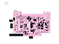
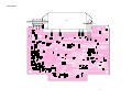
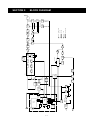
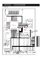
1
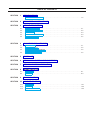
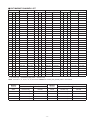
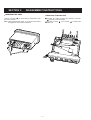
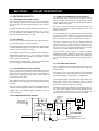
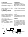
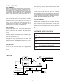
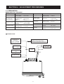
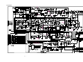
SERVICE
MANUAL
VHF MARINE TRANSCEIVER
INTRODUCTION
DANGER
This service manual describes the latest service information
for the IC-M45 VHF MARINE TRANSCEIVER at the time of
publication.
2 versions of the IC-M45 have been designed. This service
manual covers each version.
NEVER connect the transceiver to an AC outlet or to a DC
power supply that uses more than 16 V. This will ruin the
transceiver.
DO NOT expose the transceiver to rain, snow or any liquids.
DO NOT reverse the polarities of the power supply when
connecting the transceiver.
DO NOT apply an RF signal of more than 20 dBm (100mW)
to the antenna connector. This could damage the transceiver's front end.
MODEL
VERSION
USA
USA-1
IC-M45
SYNBOL
BLACK
WHITE
ORDERING PARTS
REPAIR NOTES
Be sure to include the following four points when ordering
replacement parts:
1. 10-digit order numbers
2. Component part number and name
3. Equipment model name and unit name
4. Quantity required
1. Make sure a problem is internal before disassembling
the transceiver.
2. DO NOT open the transceiver until the transceiver is disconnected from its power source.
3. DO NOT force any of the variable components. Turn
them slowly and smoothly.
4. DO NOT short any circuits or electronic parts. An insulated turning tool MUST be used for all adjustments.
5. DO NOT keep power ON for a long time when the transceiver is defective.
6. DO NOT transmit power into a signal generator or a
sweep generator.
7. ALWAYS connect a 40 dB to 50 dB attenuator between
the transceiver and a deviation meter or spectrum analyzer when using such test equipment.
8. READ the instructions of test equipment thoroughly
before connecting equipment to the transceiver.
<SAMPLE ORDER>
1110003490 S.IC TA31136FN
IC-M45 MAIN UNIT 5 pieces
8810008660 Screw PH BO M3x8 NI IC-M45 Chassis
10 pieces
Addresses are provided on the inside back cover for your
convenience.
TABLE OF CONTENTS
SECTION
1
SPECIFICATIONS
VHF MARINE CHANNEL LIST . . . . . . . . . . . . . . . . . . . . . . . . . . . . . . . . . . . . . . . . . . . . . . .1-2
SECTION
2
DISASSEMBLY INSTRUCTIONS
SECTION
3
CIRCUIT DESCRIPTION
SECTION
3-1
RECEIVER CIRCUITS . . . . . . . . . . . . . . . . . . . . . . . . . . . . . . . . . . . . . . . . . . . . . . . . . . . . .3-1
3-2
TRANSMITTER CIRCUITS . . . . . . . . . . . . . . . . . . . . . . . . . . . . . . . . . . . . . . . . . . . . . . . . .3-2
3-3
PLL CIRCUITS
3-4
POWER SUPPLY CIRCUITS . . . . . . . . . . . . . . . . . . . . . . . . . . . . . . . . . . . . . . . . . . . . . . . .3-3
3-5
PORT ALLOCATIONS . . . . . . . . . . . . . . . . . . . . . . . . . . . . . . . . . . . . . . . . . . . . . . . . . . . . .3-4
4
. . . . . . . . . . . . . . . . . . . . . . . . . . . . . . . . . . . . . . . . . . . . . . . . . . . . . . . . . .3-3
ADJUSTMENT PROCEDURES
4-1
PREPARATION . . . . . . . . . . . . . . . . . . . . . . . . . . . . . . . . . . . . . . . . . . . . . . . . . . . . . . . . . .4-1
4-2
PLL ADJUSTMENTS . . . . . . . . . . . . . . . . . . . . . . . . . . . . . . . . . . . . . . . . . . . . . . . . . . . . . .4-2
4-3
TRANSMITTER ADJUSTMENTS . . . . . . . . . . . . . . . . . . . . . . . . . . . . . . . . . . . . . . . . . . . . .4-2
4-4
RECEIVER ADJUSTMENT . . . . . . . . . . . . . . . . . . . . . . . . . . . . . . . . . . . . . . . . . . . . . . . . . .4-2
SECTION
5
PARTS LIST
SECTION
6
MECHANICAL PARTS AND DISASSEMBLY
SECTION
7
SEMI-CONDUCTOR INFORMATION
SECTION
8
BOARD LAYOUTS
8-1
LOGIC UNIT . . . . . . . . . . . . . . . . . . . . . . . . . . . . . . . . . . . . . . . . . . . . . . . . . . . . . . . . . . . . .8-1
8-2
MAIN UNIT . . . . . . . . . . . . . . . . . . . . . . . . . . . . . . . . . . . . . . . . . . . . . . . . . . . . . . . . . . . . . .8-3
SECTION
9
BLOCK DIAGRAM
SECTION
10 VOLTAGE DIAGRAM
10-1
LOGIC UNIT . . . . . . . . . . . . . . . . . . . . . . . . . . . . . . . . . . . . . . . . . . . . . . . . . . . . . . . . . . . . .10-1
10-2
MAIN UNIT . . . . . . . . . . . . . . . . . . . . . . . . . . . . . . . . . . . . . . . . . . . . . . . . . . . . . . . . . . . . . .10-2
10-3
VR-A AND VR-B UNITS . . . . . . . . . . . . . . . . . . . . . . . . . . . . . . . . . . . . . . . . . . . . . . . . . . . .10-3
SECTION 1
SPECIFICATIONS
‘ GENERAL
• Frequency coverage
: 156.025–157.425 MHz (Tx)
156.025–163.275 MHz (Rx)
• Mode
: 16K0G3E (FM)
• Usable channels
: All USA, international and Canadian channels
plus 10 weather channels*
• Power supply requirement
: 13.8 V DC ±15% (negative ground)
*USA versions only
• Usable temperature range
: –20˚C to +60˚C; –4˚F to +140˚F
• Frequency stability
: ±10 ppm (–20˚C to +60˚C; –4˚F to +140˚F)
• Current drain (at 13.8 V DC)
: Transmit
Receive
• Antenna impedance
: 50 Ω (nominal)
• Dimensions (projections not included)
: 152(W)×67(H)×144(D) mm; 6(W)×25⁄8(H)×52⁄3(D) in
• Weight (with ant., battery case and cells)
: 900 g; 2 lb
at 25 W
max. audio
6.0 A
1.2 A
‘ TRANSMITTER
• Output power (at 13.8 V DC)
: High
Low
25 W
1W
• Modulation
: Variable reactance frequency modulation
• Maximum frequency deviation
: ±5.0 kHz
• Spurious emissions
: 70 dB
• Adjacent channel power
: 60 dB
• Residual modulation
: 40 dB
• Audio harmonic distortion
: Less than 10% at 70% deviation
• Audio frequency response
: +1 dB to –3 dB of 6 dB octave from 300 Hz to 3000 Hz
‘ RECEIVER
• Receive system
: Double conversion superheterodyne system
• Intermediate frequencies
: 1st
2nd
• Sensitivity
: 0.22 µV typical at 12 dB SINAD
30.85 MHz
450 kHz
• Squelch sensitivity
: 0.22 µV typical
• Adjacent channel selectivity
: 70 dB typical
• Spurious response
: 70 dB typical
• Intermodulation rejection ratio
: 70 dB typical
• Hum and noise
: 40 dB
• Audio output power (at 13.8 V DC)
: 4.0 W typical at 10% distortion with an 4 Ω load
• Audio frequency responce
: +2 dB to –8 dB of –6 dB octave from 300 Hz to 3000 Hz
All stated specifications are subject to change without notice or obligation.
1-1
‘ VHF MARINE CHANNEL LIST
Channel No.
USA INT CAN
01
01
01A
156.050
160.650
156.050
156.050
21A
157.050
157.050
73
73
73
156.675
156.675
157.100
161.700
74
74
74
156.725
156.725
22A
157.100
157.100
77*
77
77*
156.875
156.875
23
157.150
161.750
156.925
161.525
157.150
157.150
156.925
156.925
156.975
161.575
156.975
156.975
157.025
161.625
157.025
157.025
157.075
161.675
157.075
157.075
157.125
161.725
82A
157.125
157.125
21A
22
Channel No.
USA INT CAN
156.100
160.700
03
03
156.150
160.750
156.150
156.150
23A
156.200
160.800
24
24
24
157.200
161.800
156.200
156.200
25
25
25
157.250
161.850
156.250
160.850
26
26
26
157.300
161.900
05A
156.250
156.250
27
27
27
157.350
161.950
06
156.300
156.300
28
28
28
157.400
162.000
156.350
160.950
60
60
156.025
160.625
07A
156.350
156.350
61
156.075
160.675
156.075
156.075
156.125
160.725
156.125
156.125
83A
156.175
160.775
84
156.175
156.175
84A
64
156.225
160.825
85
64A
156.225
156.225
85A
04A
05
05A
06
07
07A
08
08
08
156.400
156.400
09
09
09
156.450
156.450
10
10
10
156.500
156.500
11
11
11
156.550
156.550
12
12
156.600
156.600
13*
13
13*
156.650
156.650
14
14
14
156.700
156.700
2
Frequency (MHz)
Transmit
Receive
02
04
12
Channel No.
USA INT CAN
02
03A
06
Frequency (MHz)
Receive
Transmit
1
22A
23
61A
61A
62
62A
63
63A
64
64A
1
78
79
79A
80A
81
82A
83
156.750
65
156.275
160.875
86
16
16
16
156.800
156.800
65A 65A 65A
156.275
156.275
86A
17
17*
156.850
156.850
66
156.325
160.925
87
156.900
161.500
66A 66A 66A*1
156.325
156.325
87A
156.900
156.900
67*
67
67
156.375
156.375
88
156.950
161.550
68
68
68
156.425
156.425
88A
19A
156.950
156.950
69
156.475
156.475
20
157.000
161.600
70*
70*
70*
156.525
156.525
157.000
157.000
71
71
71
156.575
156.575
157.050
161.650
72
72
72
156.625
156.625
17*
1
18
18A
18A
19
19A
20
20
20A
21
21
2
69
69
3
3
3
81A
82
156.750
1
80A
81A
15*
1
79A
80
15*
1
78A
78A
15*
2
1
84
85
86
87
88
Frequency (MHz)
Receive
Transmit
83
157.175
161.775
83A
157.175
157.175
84
157.225
161.825
157.225
157.225
157.275
161.875
157.275
157.275
157.325
161.925
157.325
157.325
157.375
161.975
157.375
157.375
157.425
162.025
157.425
157.425
85
86
87
88
*1 Low power only, *2 Momentary high power, *3 Receive only
NOTE: Channels 3, 21, 23, 61, 64, 81, 82 and 83 CANNOT be used by the general public in USA waters.
Weather
channel
Frequency (MHz)
Transmit
Receive
Weather
channel
Frequency (MHz)
Transmit
Receive
WX01
Receive only
162.550
WX06
Receive only
162.500
WX02
Receive only
162.400
WX07
Receive only
162.525
WX03
Receive only
162.475
WX08
Receive only
161.650
WX04
Receive only
162.425
WX09
Receive only
161.775
WX05
Receive only
162.450
WX10
Receive only
163.275
1-2
SECTION 2
DISASSEMBLY INSTRUCTIONS
• REMOVING THE CASE
• REMOVING THE MAIN UNIT
Unsolder DC cable (2 points) and antenna connector,
(3 points), as shown below.
Unscrew 2 screws,
, and 7 screws,
, to remove the
MAIN unit.
Unscrew 4 screws,
, as shown below, and slide the case
free of the chassis.
Note: When replacing the screw, 10–12 kg of torque MUST
be applied to ensure water resistance.
C
D
A
2-1
B
SECTION 3
CIRCUIT DESCRIPTION
3-1 RECEIVER CIRCUITS
3-1-4 2ND IF AND DEMODULATOR CIRCUITS
3-1-1 ANTENNA SWITCHING CIRCUIT
The 2nd mixer circuit converts the 1st IF signal to a 2nd IF
signal. A double superheterodyne system (which converts
receive signals twice) improves the image rejection ratio and
obtains stable receiver gain.
The antenna switching circuit functions as a low-pass filter
while receiving and as resonator circuit while transmitting.
The circuit does not allow transmit signals to enter receiver
circuits.
The FM IF IC (IC1) contains the 2nd local oscillator, 2nd
mixer, limiter amplifier, quadrature detector, and noise
detector circuits, etc.
Received signals enter the MAIN unit from the antenna connector and pass through the low-pass filter (L1–L3, C1–C5,
C7). The signals are then applied to the RF circuit via the
antenna switching circuit (D1, L4, L25).
The 1st IF signal from Q3 is applied to the 2nd mixer section
of IC1 (pin 16), and is mixed with a 30.4 MHz 2nd LO signal
generated at the PLL circuit by doubling the reference frequency (15.2 MHz) to produce a 450 kHz 2nd IF signal.
3-1-2 RF CIRCUIT
The RF circuit amplifies signals within the range of frequency coverage and filters out-of-band signals.
The 2nd IF signal from IC1 (pin 3) is passed through the
ceramic filter (FI2), where unwanted signals are suppressed, and is then applied to the 2nd IF and limiter amplifiers in IC1 (pin 5). The signal is applied to the FM detector
section in IC1 for demodulation into AF signals.
The signals from the antenna switching circuit pass through
a tunable bandpass filter (D2, L5) where the object signals
are led to the RF amplifier circuit (Q1).
The FM detector circuit employs a quadrature detection
method (linear phase detection), which uses a ceramic discriminator (X2) for phase delay to obtain a non-adjusting circuit. The detected signal from IC1 (pin 9) is applied to the AF
circuit.
The amplified signals at Q1 are applied to the 2-stage tunable bandpass filter (D3, D4, L6, L7) to suppress unwanted
signals and improve the selectivity. The signals are then
applied to the 1st mixer circuit.
D2–D4 employ varactor diodes, that are controlled by the
PLL lock voltage, to track the band pass filters.
3-1-5 AF AMPLIFIER CIRCUIT
The AF amplifier circuit amplifies the detected signals to
drive a speaker. The AF circuit includes an AF mute circuit
for the squelch.
3-1-3 1ST MIXER AND 1ST IF CIRCUITS
The 1st mixer circuit converts the received signal to a fixed
frequency of the 1st IF signal with a 1st LO (VCO output) frequency. By changing the 1st LO frequency, only the desired
frequency will be passed through a pair of crystal filters at
the next stage of the mixer.
AF signals from IC1 (pin 9) are applied to the de-emphasis
circuit (R92, C152). The de-emphasis circuit is an integrated
circuit with frequency characteristic of –6 dB/octave.
The integrated signals are applied to the active filters (Q21,
Q22). Q21 functions as a high-pass filter to suppress
unwanted lower noise signals and Q22 functions as a lowpass filter to suppress higher noise signals.
The signals from the RF circuit are mixed with the VCO signals at the 1st mixer circuit (Q2) to produce a 30.85 MHz 1st
IF signal.
The 1st IF signal is applied to a pair of crystal filters (FI1) to
suppress out-of-band signals and is then amplified at the IF
amplifier (Q3). The amplified signal is applied to the 2nd
mixer circuit (IC1).
The filtered signals are passed through the [VOLUME] control, and are then applied to the AF power amplifier (IC9, pin
1) via the analog switch (IC5, pins 4, 3). The output signal
from IC9 (pin 4) drives the internal (external) speaker.
• 2nd IF AND DEMODULATOR CIRCUITS
2nd IF filter
450 kHz
8
7
5
10
17
2 16
2
PLL IC
IC3
Mixer
Limiter
amp.
FM
detector
9
3
Noise
detector
Active
filter
AF signal "DET"
(30.4 MHz)
FI2
X1
15.2 MHz
RSSI
Squelch level
adjustment pot
R1 (VR-B unit)
11
13
IC1 TA31136F
1st IF (30.85 MHz)
from Q3
"SQL" signal to the CPU pin 22
X2
R5
3-1
16
3-1-6 SQUELCH CIRCUIT
3-2-2 MODULATION CIRCUIT
A squelch circuit cuts out AF signals when no RF signals are
received. By detecting noise components in the AF signals,
the squelch circuit switches the AF mute switch.
The modulation circuit modulates the VCO oscillating signal
(RF signal) using the microphone audio signals.
Audio signals from the splatter filter (IC6b) pass through the
frequency deviation adjustment pot (R130) and are then
applied to the modulation circuit (D7) to change the reactance of D7, and modulate the oscillated signal at the TXVCO (Q4).
A portion of the AF signals from the FM IF IC (IC1, pin 9)
pass through the [SQUELCH] control pot, and are then
applied to the active filter section (IC1, pin 8). The active filter section amplifies and filters noise components. The filtered signals are applied to the noise detector section and
output from pin 13 as the “SQL” signal. The “SQL” signal is
applied to the CPU (LOGIC unit; IC1, pin 22). The CPU analyzes the noise condition and outputs the RMUT signal via
the I/O expander IC (IC7) to toggle the analog switches (IC5,
pins 4, 3) as an AF mute switch.
3-2-3 DRIVE AMPLIFIER CIRCUIT
The drive amplifier circuit amplifies the VCO oscillating signal to a level needed at the power amplifier.
The VCO output is buffer-amplified by Q7 and Q9, and is
then applied to the T/R switch (D9). The transmit signal from
the T/R switch is amplified to the pre-drive (Q10) and drive
(Q11) amplifiers to obtain an approximate 400 mW signal
level. The amplified signal is then applied to the RF power
amplifier (IC2).
3-1-7 WEATHER ALERT DECODER CIRCUIT
[USA version only]
When the weather alert function is activated and a 1050 Hz
alert tone from an NOAA weather radio broadcast is
received, the IC-M45 emits beep tones and indicates flashing “ALT” on the display to inform of an emergency weather
report on the air.
3-2-4 POWER AMPLIFIER CIRCUIT
The power amplifier circuit amplifies the driver signal to an
output power level.
AF signals from the FM IF IC (IC1, pin 9) are applied to the
tone decoder (IC10, pin 3). When a 1050 Hz signal is detected, the tone decoder outputs a low level signal from pin 8
and the output signals are applied to the CPU (LOGIC unit;
IC1) to control beep tones and the “ALT” indicator.
IC2 is a power module which has amplification output capabilities of about 35 W. The output from IC2 (pin 4) is passed
through the antenna switching circuit (D13) and is then
applied to the antenna connector via the low-pass filter.
3-2 TRANSMITTER CIRCUITS
3-2-5 APC CIRCUIT
3-2-1 MICROPHONE AMPLIFIER CIRCUIT
The APC circuit stabilizes transmit output power.
The microphone amplifier circuit amplifies audio signals with
+6 dB/octave pre-emphasis from the microphone to a level
needed at the modulation circuit.
The AF signals from the microphone are amplified at the
microphone amplifier (IC4). A capacitor (C135) and resistor
(R114) are connected to the amplifier to obtain the preemphasis characteristics.
The RF output signal from the power amplifier (IC2) is
detected at the power detector circuit (D11, D12, L22) and is
then applied to one of the differential amplifier inputs (Q13,
pin 5) via the High/Low control circuit (R70, R71, Q16). The
applied voltage controls the differential amplifier output
(Q17, pin 2) and the bias voltage control (Q12). Thus the
APC circuit maintains a constant output power.
The amplified signals are applied to the IDC amplifier (IC6a,
pin 2) via the analog switch (IC5, pins 8, 9) and are passed
through the splatter filter (IC6b) to suppress unwanted 3 kHz
or higher signals. The filtered signals are then applied to the
modulation circuit.
The reflected power from the antenna connector is detected
at D12 and is then applied to the CPU. The detected voltage
increases when the antenna is mismatched, causing the
output power to be switched from High to Low to protect the
power module (IC2).
• APC circuit
RF signal
from PLL
L22
Q11
Drive
amp.
Power module
IC2
D11
TMUT
D12
to antenna
RF detector
circuit
T5
HV
Q14
Q12
Q13
R71
Q15
"TXDET" signal
to the CPU
R70
Q16
HI/LO
APC control circuit
3-2
The phase detector compares the input signal with a reference frequency, and then outputs the out-of-phase signal
(pulse-type signal) from pin 13.
3-3 PLL CIRCUITS
3-3-1 GENERAL
The PLL circuit provides stable oscillation of the transmit frequency and receive 1st LO frequency. The PLL circuit compares the phase of the divided VCO frequency to the reference frequency. The PLL output frequency is controlled by a
crystal oscillator and the divided ratio of the programmable
divider. IC3 is a dual PLL IC which controls both VCO circuits for Tx and Rx.
The pulse-type signal is converted into DC voltage (lock
voltage) at the loop filter (R34, R37, R38, C64, C73), and
then applied to varactor diode (D8) of the RX-VCO to stabilize the oscillated frequency. The lockvoltage is also used for
the receiver circuit for the bandpass filter center frequency.
The lock voltage from the loop filter is amplified at the bufferamplifier (Q6) and then applied to the RF circuit.
The PLL circuit , using a one chip PLL IC (IC3), directly generates the transmit frequency and receive 1st IF frequency
with VCOs. The PLL sets the divided ratio based on serial
data from the CPU on the LOGIC unit and compares the
phases of VCO signals with the reference oscillator frequency. The PLL IC detects the out-of-step phase and output from pins 8 and 13 for Tx and Rx, respectively. The reference frequency (15.2 MHz) is oscillated at X1.
3-3-4 VCO CIRCUIT
The VCO outputs from Q4 (Tx) and Q5 (Rx) are bufferamplified at Q7 and Q9, and are then sent to the T/R switch
(D9). The receive LO signal is applied to the 1st mixer circuit
(Q2) through a low-pass filter, and the transmit signal is
applied to the pre-drive amplifier (Q10). A portion of the VCO
output is reapplied to the PLL IC (IC10, pin 2 or pin 13) via
Q8.
3-3-2 TX LOOP
The generated signal at the TX-VCO (Q4, D6, D7) enters
the PLL IC (IC3, pin 2) and is divided at the programmable
divider section and is then applied to the phase detector
section.
3-4 POWER SUPPLY CIRCUITS
The phase detector compares the input signal with a reference frequency, and then outputs the out-of-phase signal
(pulse-type signal) from pin 8.
The pulse-type signal is converted into DC voltage (lock
voltage) at the loop filter (R41–R43, C75–C77), and then
applied to varactor diodes (D6, D7) of the TX-VCO to stabilize the oscillated frequency.
LINE
DESCRIPTION
HV
The voltage from the connected DC power supply.
HVS
Same voltage as the HV line which is passed
through the [PWR] switch (VR-A unit; R1).
5V
Common 5 V converted from the HVS line at the
5V regulator circuit (IC8).
R5
Receive 5 V converted from the 5V line at the R5
regulator circuit (Q19, Q20). The regulated voltage is applied to the receiver circuits.
T5
Transmit 5 V converted from the 5V line at the T5
regulator circuit (Q17, Q18).
3-3-3 RX LOOP
The generated signal at the RX-VCO (Q5, D8) enters the
PLL IC (IC3, pin 19) and is divided at the programmable
divider section and is then applied to the phase detector
section.
• PLL circuit
Buffer
TX VCO
D9
to transmitter circuit
Q9
Buffer
Q4, D6, D7
to 1st mixer circuit
Q7
Buffer
RX VCO
Q8
Q5, D8
Loop
filter
IC3 (PLL IC)
Phase
detector
8
30.4 MHz signal
to the FM IF IC
X1
15.2 MHz
17
×2
Programmable
counter
Programmable
divider
Prescaler
Shift register
16
3-3
2
3
4
5
P.STB
CK
DATA
3-5 PORT ALLOCATIONS
3-5-2 OUTPUT EXPANDER (MAIN unit; IC7)
3-5-1 CPU (LOGIC unit; IC1)
Pin
number
Port
name
Description
Pin
number
Port
name
Description
3
LBATT
Input port for the connected power
supply voltage detection (low battery
indicator).
4
RCV
Outputs the R5 regulator (Q19, Q20)
control signal.
Low : While receiving
5
PTT.M
Input port for the PTT switch.
5
SEND
Outputs the T5 regulator (Q17, Q18)
control signal.
Low : While transmitting
11
HI/LO
Output port fo RF output power (High
or Low) select signal.
Low : While low power is selected
12
OP.RST
Outputs the reset signal for optional
unit via J5 (MAIN unit).
13
RMUT
Outputs the analog switch (IC5) control signal.
Low : While squelched
14
TMUT
Outputs transmit mute signal.
Low : While transmitting
6
7
8
TXDET
Input port for the “TX” indicator from
the power detector circuit (Main unit;
D11, D12).
SQLV
Input port for the squelch volume level.
KEY.M
Input port for the smart mic functions.
2.02 V: [UP] is pushed
3.00 V: [DN] is pushed
3.84 V: [HI/LO] is pushed
Outputs beep audio signals.
10
BEEP
13
OEX.STB
Outputs strobe signals for the output
expander (MAIN unit; IC7).
14
P.STB
Outputs strobe signals for the PLL circuit.
15
DATA
Outputs data signals to the EEPROM
(IC4), PLL IC (MAIN unit; IC3) and
expander ICs (MAIN unit; IC7), etc.
16
CK
Outputs clock signal to the EEPROM
(IC4), PLL IC (MAIN unit; IC3) and
expander ICs (MAIN unit; IC7), etc.
17
ESI
Input port for the data signals from the
EEPROM (IC4).
22
SQL
Input port from the FM IF IC (MAIN
unit; IC1) for the squelch operation.
23
UNLK
Input port for the PLL unlock signal.
Low : While PLL is locked.
TONE
Input port for the weather alert tone
decode signal.
Low : Weather alert tone (1050 Hz)
is detected.
24
26, 27
LAMP2, Outputs LCD backlight control signal.
High : While LCD backlight is ON.
LAMP1
31
HANG
Input port for the microphone hanger
detection signal.
Low : Microphone on hook
33
DOWN
Input port for the [DOWN] switch.
34
UP
Input port for the [UP] switch.
35
H/L
Input port for the [H/L] switch.
36
SCAN
Input port for the [SCAN] switch.
37
CH/WX
Input port for the [CH/WX] switch.
38
CH16/9 Input port for the [16/9] switch.
3-4
SECTION 4 ADJUSTMENT PROCEDURES
4-1 PREPARATION
■ REQUIRED TEST EQUIPMENT
EQUIPMENT
GRADE AND RANGE
EQUIPMENT
DC power supply
Output voltage
Current capacity
: 13.8 V DC
: 10 A or more
RF power meter
(terminated type)
Measuring range
Frequency range
Impedance
SWR
:
:
:
:
Frequency counter
Frequency range
: 0.1–300 MHz
Frequency accuracy : ±1 ppm or better
Sensitivity
: 100 mV or better
FM deviation meter
Frequency range
Measuring range
DC voltmeter
Input impedance
GRADE AND RANGE
Frequency range
Measuring range
: 300–3000 Hz
: 1–500 mV
Frequency range
Output level
: 0.1–300 MHz
: 0.1 µV–32 mV
(–127 to –17 dBm)
Oscilloscope
Frequency range
Measuring range
: DC–20 MHz
: 0.01–20 V
AC millivoltmeter
Measuring range
: 10 mV–10 V
: 30–300 MHz
: 0 to ±10 kHz
External speaker
Input impedance
Capacity
:4Ω
: 5 W or more
: 50 kΩ/V DC or better
Attenuator
Power attenuation
Capacity
: 50 or 60 dB
: 50 W or more
Audio generator
1–50 W
100–300 MHz
50 Ω
Less than 1.2 : 1
Standard signal
generator (SSG)
‘ CONNECTIONS
Standard signal
generator
–17 to –125 dBm
(32 mV to 0.13 µV)
CAUTION:
DO NOT transmit while SSG is
connected to the antenna connector.
+
RF power meter
50 Ω / 1–50 W
FM deviation
meter
–
Frequency
counter
to DC cable
Red
Attenuator
50 dB or 60 dB
to the antenna connector
4-1
DC power supply
13.8 V /15 A
Black
4-2 PLL ADJUSTMENTS
ADJUSTMENT
ADJUSTMENT CONDITION
MEASUREMENT
UNIT
LOCK
VOLTAGE
1 • Operating channel : ch16
• Receiving
MAIN
2 • Operating channel : ch16
• Output power
: Low
• Transmitting
REFERENCE 1 • Operating channel : ch16
• Output power
: Low
FREQUENCY
• Connect an RF power meter or a
50 Ω dummy load to the antenna
connector.
• Transmitting
VALUE
LOCATION
Connect a digital 2.6 V
multi-meter or oscilloscope
to
the
check point CP1.
ADJUSTMENT
POINT
UNIT
ADJUST
MAIN
L13
Connect a digital 2.8 V
multi-meter or oscilloscope
to
the
check point CP2.
Rear
Panel
L12
Loosely couple the 156.800000 MHz
frequency counter
to the antenna connector.
MAIN
C117
4-3 TRANSMITTER ADJUSTMENTS
ADJUSTMENT
ADJUSTMENT CONDITION
MEASUREMENT
UNIT
OUTPUT
POWER
1 • Operating channel : ch16
• Output power
: Low
• Transmitting
2 • Output power
• Transmitting
Rear
Panel
Connect an RF 1 W
power meter to the
antenna connector.
UNIT
ADJUST
MAIN
R70
25 W
: High
FREQUENCY 1 • Operating channel : ch16
• Output power
: Low
DEVIATION
• Connect an audio generator to J2
(pin 5) with an AC millivoltmeter
and set as:
Frequency
: 1 kHz
Level
: 550 mV
• Set an FM deviation meter as:
HPF
: OFF
LPF
: 20 kHz
De-emphasis
: OFF
Detector
: (P–P)/2
• Transmitting
VALUE
LOCATION
ADJUSTMENT
POINT
Rear
Panel
R71
Connect an FM ±4.3 kHz
deviation meter to
the antenna connector through an
attenuator.
MAIN
R130
4-4 RECEIVER ADJUSTMENT
ADJUSTMENT
ADJUSTMENT CONDITION
MEASUREMENT
UNIT
SENSITIVITY 1 • Operating channel : ch16
• [SQUELCH] control:
Max. counterclockwise
• Connect an SSG to the antenna
connector and set as:
Frequency
: 156.800 MHz
Level
: 10 µV*
(–97 dBm)
Modulation
: 1 kHz
Deviation
: ±3.5 kHz
• Receiving
MAIN
VALUE
LOCATION
Connect a DC volt- Maximum voltage
meter to the check
point CP3.
*This output level of a standard signal generator (SSG) is indicated as SSG’s open circuit.
4-2
ADJUSTMENT
POINT
UNIT
ADJUST
MAIN
L5,
L6,
L7,
+
–
DC power supply
13.8 V /15 A
to DC cable
Red
Black
R70 Output power
adjustment for [Low]
R71
Output power
adjustment for [High]
L5
R130
L6
Frequency deviation
adjustment
Sensitivity
adjustment
L7
C117
Reference frequency
adjustment
CP1 PLL lock voltage
check point for [RX]
CP2 PLL lock voltage
check point for [TX]
CP3 Sensitivity
check point
L12 PLL lock voltage
adjustment for [TX]
L13 PLL lock voltage
adjustment for [RX]
J2
1
7
J2
Audio generator +
300 Hz to 3 kHz –
w
y
t
r
[PTT]
AC millivoltmeter
2–200 mV
4-3
SECTION 5 PARTS LIST
[LOGIC UNIT]
REF
NO.
[LOGIC UNIT]
ORDER
NO.
REF
NO.
DESCRIPTION
IC1
IC2
IC3
IC4
1140007220
1110003500
1130007390
1140005620
S.IC
S.IC
S.IC
S.IC
M38223M4-432-HP
S-80742SL-A6-T1
TC7W02F (TE12L)
X25080SI-2.7T6
Q1
Q2
Q3
Q4
Q5
1530001950
1510000500
1530001950
1590000670
1520000450
S.TRANSISTOR
S.TRANSISTOR
S.TRANSISTOR
S.TRANSISTOR
S.TRANSISTOR
2SC2712-GR (TE85R)
2SA1162-GR (TE85R)
2SC2712-GR (TE85R)
FMW1 T148
2SB1132 T100 Q
D1
D2
D3
D4
1750000060
1750000110
1750000060
1750000060
S.DIODE
S.DIODE
S.DIODE
S.DIODE
1SS196
1SS272
1SS196
1SS196
(TE85R)
(TE85R)
(TE85R)
(TE85R)
X1
6060000630 S.CERAMIC
PBRC 4.91 BR
R1
R2
R3
R4
R5
R6
R7
R8
R9
R10
R11
R12
R13
R14
R15
R16
R17
R18
R19
R20
R21
R22
R23
R24
R25
R26
R27
R28
R29
R30
R31
R32
R33
R34
7030003560
7030003680
7030003680
7030003680
7030003440
7030003760
7030003720
7030003720
7030003680
7030003620
7030003540
7030003640
7030003560
7030003680
7030003640
7030003640
7030003640
7030000190
7030000190
7030003660
7030003640
7030003630
7030003650
7030003440
7030003510
7030003490
7030003700
7030003640
7030003560
7030003560
7030003640
7030003640
7030003640
7030003640
S.RESISTOR
S.RESISTOR
S.RESISTOR
S.RESISTOR
S.RESISTOR
S.RESISTOR
S.RESISTOR
S.RESISTOR
S.RESISTOR
S.RESISTOR
S.RESISTOR
S.RESISTOR
S.RESISTOR
S.RESISTOR
S.RESISTOR
S.RESISTOR
S.RESISTOR
S.RESISTOR
S.RESISTOR
S.RESISTOR
S.RESISTOR
S.RESISTOR
S.RESISTOR
S.RESISTOR
S.RESISTOR
S.RESISTOR
S.RESISTOR
S.RESISTOR
S.RESISTOR
S.RESISTOR
S.RESISTOR
S.RESISTOR
S.RESISTOR
S.RESISTOR
ERJ3GEYJ 103 V (10 kΩ)
ERJ3GEYJ 104 V (100 kΩ)
ERJ3GEYJ 104 V (100 kΩ)
ERJ3GEYJ 104 V (100 kΩ)
ERJ3GEYJ 102 V (1 kΩ)
ERJ3GEYJ 474 V (470 kΩ)
ERJ3GEYJ 224 V (220 kΩ)
ERJ3GEYJ 224 V (220 kΩ)
ERJ3GEYJ 104 V (100 kΩ)
ERJ3GEYJ 333 V (33 kΩ)
ERJ3GEYJ 682 V (6.8 kΩ)
ERJ3GEYJ 473 V (47 kΩ)
ERJ3GEYJ 103 V (10 kΩ)
ERJ3GEYJ 104 V (100 kΩ)
ERJ3GEYJ 473 V (47 kΩ)
ERJ3GEYJ 473 V (47 kΩ)
ERJ3GEYJ 473 V (47 kΩ)
MCR10EZHJ 27 Ω (270)
MCR10EZHJ 27 Ω (270)
ERJ3GEYJ 683 V (68 kΩ)
ERJ3GEYJ 473 V (47 kΩ)
ERJ3GEYJ 393 V (39 kΩ)
ERJ3GEYJ 563 V (56 kΩ)
ERJ3GEYJ 102 V (1 kΩ)
ERJ3GEYJ 392 V (3.9 kΩ)
ERJ3GEYJ 272 V (2.7 kΩ)
ERJ3GEYJ 154 V (150 kΩ)
ERJ3GEYJ 473 V (47 kΩ)
ERJ3GEYJ 103 V (10 kΩ)
ERJ3GEYJ 103 V (10 kΩ)
ERJ3GEYJ 473 V (47 kΩ)
ERJ3GEYJ 473 V (47 kΩ)
ERJ3GEYJ 473 V (47 kΩ)
ERJ3GEYJ 473 V (47 kΩ)
C1
C2
C3
C4
C5
C6
C7
C8
C9
C10
C11
C12
C13
C14
C15
C16
C17
C18
4030006860
4030006860
4030006900
4030006900
4030006900
4030006900
4030009660
4030006900
4030006900
4510005860
4030006900
4030006900
4030006900
4030008630
4030008630
4030008630
4030006900
4030006900
S.CERAMIC
S.CERAMIC
S.CERAMIC
S.CERAMIC
S.CERAMIC
S.CERAMIC
S.CERAMIC
S.CERAMIC
S.CERAMIC
S.ELECTROLYTIC
S.CERAMIC
S.CERAMIC
S.CERAMIC
S.CERAMIC
S.CERAMIC
S.CERAMIC
S.CERAMIC
S.CERAMIC
C1608 JB 1H 102K-T-A
C1608 JB 1H 102K-T-A
C1608 JB 1E 103K-T-A
C1608 JB 1E 103K-T-A
C1608 JB 1E 103K-T-A
C1608 JB 1E 103K-T-A
C1608 JF 1C 224Z-T-A
C1608 JB 1E 103K-T-A
C1608 JB 1E 103K-T-A
ECEV1HA2R2SR
C1608 JB 1E 103K-T-A
C1608 JB 1E 103K-T-A
C1608 JB 1E 103K-T-A
C1608 JF 1C 104Z-T-A
C1608 JF 1C 104Z-T-A
C1608 JF 1C 104Z-T-A
C1608 JB 1E 103K-T-A
C1608 JB 1E 103K-T-A
ORDER
NO.
DESCRIPTION
C19
C20
C21
4030006900 S.CERAMIC
4030006900 S.CERAMIC
4030006900 S.CERAMIC
C1608 JB 1E 103K-T-A
C1608 JB 1E 103K-T-A
C1608 JB 1E 103K-T-A
DS1
DS2
DS3
5030001373 LCD
5080000170 LAMP
5080000170 LAMP
LD-HU4549J-1
HRS-7219A-Y2-30
HRS-7219A-Y2-30
J1
J2
6510019070 S.CONNECTOR
6510018960 S.CONNECTOR
52559-3092
B2B-PH-SM3-TB
W3
8900005320 FFC
OPC-519
EP1
EP2
0910049094 PCB
8930045650 LCD CONTACT
B 5035D
SRCN-2040-SP-N-W
[VR-A UNIT]
REF
NO.
ORDER
NO.
DESCRIPTION
R1
7210001500 VARIABLE
RK097111102AA (10KA)
W1
8900007790 CABLE
OPC-759
EP1
0910049102 PCB
B 5036B
[VR-B UNIT]
REF
NO.
ORDER
NO.
DESCRIPTION
R1
7210001010 VARIABLE
RK097111000AA (10KB)
EP1
0910049312 PCB
B 5055B
[MAIN UNIT]
REF
NO.
ORDER
NO.
DESCRIPTION
IC1
IC2
IC3
IC4
IC5
IC6
IC7
IC8
IC9
IC10
1110003490
1150001540
1130007610
1130007370
1130007690
1110003750
1130007700
1180001070
1110003090
1110003640
S.IC
IC
S.IC
S.IC
S.IC
S.IC
S.IC
S.IC
IC
S.IC
TA31136FN (D,EL)
M57710-A/SC-1302
µPD3140GS-E1 (DS8)
TA75S558F (TE85L)
BU4066BCF-T1
M5218AFP 600C
BU4094BCF-T1
TA7805F (TE16L)
LA4425A
BA1604F-T
Q1
Q2
Q3
Q4
Q5
Q6
Q7
1560000550
1580000540
1530002360
1560000330
1560000330
1560000540
1530002600
S.FET
S.FET
S.TRANSISTOR
S.FET
S.FET
S.FET
S.TRANSISTOR
2SK882-Y (TE85R)
3SK131-T2-LA
2SC2714-Y (TE85R)
2SK210-GR (TE85R)
2SK210-GR (TE85R)
2SK880-Y (TE85R)
2SC4215-O (TE85R)
S.=Surface mount
5-1
[MAIN UNIT]
[MAIN UNIT]
REF
NO.
ORDER
NO.
REF
NO.
Q8
Q9
Q10
Q11
Q12
Q13
Q14
Q15
Q16
Q17
Q18
Q19
Q20
Q21
Q22
Q23
Q24
Q25
1530002600
1530002600
1530002240
1530002340
1520000380
1590000670
1590000420
1590000420
1590000460
1590000420
1520000460
1590000420
1520000460
1530000160
1530000160
1540000550
1590001190
1520000460
S.TRANSISTOR
S.TRANSISTOR
S.TRANSISTOR
S.TRANSISTOR
TRANSISTOR
S.TRANSISTOR
S.TRANSISTOR
S.TRANSISTOR
S.TRANSISTOR
S.TRANSISTOR
S.TRANSISTOR
S.TRANSISTOR
S.TRANSISTOR
S.TRANSISTOR
S.TRANSISTOR
S.TRANSISTOR
S.TRANSISTOR
S.TRANSISTOR
2SC4215-O (TE85R)
2SC4215-O (TE85R)
2SC3775-3-TB
2SC2954-T2B
2SB1143 S
FMW1 T148
RN1404 (TE85R)
RN1404 (TE85R)
RN1402 (TE85R)
RN1404 (TE85R)
2SB1132 T100 R
RN1404 (TE85R)
2SB1132 T100 R
2SC2712-Y (TE85RTEM)
2SC2712-Y (TE85RTEM)
2SD1664 T100Q
XP6501- (TX).AB
2SB1132 T100 R
D1
D2
D3
D4
D5
D6
D7
D8
D9
D10
D11
D12
D13
D16
D17
D18
D19
1710000290
1720000370
1720000370
1720000370
1750000470
1790000640
1790000640
1790000640
1790000450
1750000060
1790000690
1790000690
1710000290
1750000070
1790000700
1790000640
1790000640
DIODE
S.VARICAP
S.VARICAP
S.VARICAP
S.DIODE
S.VARICAP
S.VARICAP
S.VARICAP
S.DIODE
S.DIODE
S.DIODE
S.DIODE
DIODE
S.DIODE
DIODE
S.VARICAP
S.VARICAP
MI308
HVU350TRF
HVU350TRF
HVU350TRF
1SS321 (TE85R)
MA363B (TX)
MA363B (TX)
MA363B (TX)
MA862 (TX)
1SS196 (TE85R)
HSM88ASR-TR
HSM88ASR-TR
MI308
1SS226 (TE85R)
DSA3A1
MA363B (TX)
MA363B (TX)
FI1
FI2
2010001610 MONOLITHIC
2020001210 CERAMIC
X1
X2
6050009640 XTAL
CR-528 (15.2 MHz)
6070000210 S.DISCRIMINATOR CDBCA450CX24
L1
L2
L3
L4
L5
L6
L7
L8
L9
L10
L11
L12
L13
L14
L15
L16
L17
L18
L19
L20
L21
L22
L23
L24
L25
L26
6110001670
6110001600
6110001130
6110001600
6150004360
6150004360
6150004360
6200004790
6200002430
6200003320
6200003100
6130002370
6130002360
6200003090
6200003090
6200004700
6200004700
6200004700
6200002430
6200002430
6170000230
6110001600
6200004660
6200004660
6110001580
6200002600
COIL
COIL
COIL
COIL
S.COIL
S.COIL
S.COIL
S.COIL
S.COIL
S.COIL
S.COIL
S.COIL
S.COIL
S.COIL
S.COIL
S.COIL
S.COIL
S.COIL
S.COIL
S.COIL
COIL
COIL
S.COIL
S.COIL
COIL
S.COIL
LA-253
LA-243
LA-149
LA-243
LS-491
LS-491
LS-491
MLF1608D R47K-T
NL 252018T-082J
NL 322522T-3R3J-3
NL 322522T-3R9J-3
LB-258
LB-257
NL 322522T-2R7J-3
NL 322522T-2R7J-3
MLR1608M R10K-T
MLR1608M R10K-T
MLR1608M R10K-T
NL 252018T-082J
NL 252018T-082J
LW-25
LA-243
MLF1608A 1R8K-T
MLF1608A 1R8K-T
LA-238
NL 252018T-047J
R1
R2
R3
R4
R5
R6
R7
7030003280
7030003320
7030003800
7030003800
7030003800
7030003680
7030003320
S.RESISTOR
S.RESISTOR
S.RESISTOR
S.RESISTOR
S.RESISTOR
S.RESISTOR
S.RESISTOR
ERJ3GEYJ
ERJ3GEYJ
ERJ3GEYJ
ERJ3GEYJ
ERJ3GEYJ
ERJ3GEYJ
ERJ3GEYJ
DESCRIPTION
R8
R9
R10
R11
R12
R13
R14
R15
R17
R18
R19
R20
R21
R22
R23
R24
R25
R26
R27
R28
R29
R30
R31
R32
R33
R34
R35
R36
R37
R38
R39
R40
R41
R42
R43
R44
R45
R46
R47
R48
R49
R50
R51
R52
R53
R54
R55
R56
R57
R58
R59
R60
R61
R62
R63
R64
R65
R66
R67
R68
R69
R70
R71
R72
R73
R74
R75
R76
R77
R78
R79
R80
R81
R82
R83
R84
R85
R86
R87
R88
R89
R90
FL-202 (30.850 MHz)
CFWS450E
470
101
105
105
105
104
101
V
V
V
V
V
V
V
(47 Ω)
(100 Ω)
(1 MΩ)
(1 MΩ)
(1 MΩ)
(100 kΩ)
(100 Ω)
ORDER
NO.
7030003790
7030003600
7030003680
7030003560
7030003200
7030003350
7030003280
7030003480
7030003410
7030003460
7030003680
7030003400
7030003460
7030003390
7030003450
7030003680
7030003400
7030003690
7030003620
7030003490
7030003610
7030003680
7030003280
7030003280
7030003310
7030003440
7030003440
7030003440
7030003440
7030003590
7030003560
7030003640
7030003410
7030003550
7030003560
7030003380
7030003380
7030003420
7030003660
7030003420
7030003660
7030003390
7030003630
7030003440
7030003320
7030003320
7030003480
7030003520
7030003520
7030003320
7030003200
7030003440
7030003320
7030003440
7030003220
7030003220
7030000240
7030003480
7030003480
7030003680
7030003460
7310002740
7310002670
7030003560
7030003360
7030003480
7030003500
7030003560
7030003640
7030003320
7410000990
7410000990
7030003280
7030003280
7030003280
7030003640
7030003640
7030003640
7030003640
7030003560
7030003480
7030003560
DESCRIPTION
S.RESISTOR
S.RESISTOR
S.RESISTOR
S.RESISTOR
S.RESISTOR
S.RESISTOR
S.RESISTOR
S.RESISTOR
S.RESISTOR
S.RESISTOR
S.RESISTOR
S.RESISTOR
S.RESISTOR
S.RESISTOR
S.RESISTOR
S.RESISTOR
S.RESISTOR
S.RESISTOR
S.RESISTOR
S.RESISTOR
S.RESISTOR
S.RESISTOR
S.RESISTOR
S.RESISTOR
S.RESISTOR
S.RESISTOR
S.RESISTOR
S.RESISTOR
S.RESISTOR
S.RESISTOR
S.RESISTOR
S.RESISTOR
S.RESISTOR
S.RESISTOR
S.RESISTOR
S.RESISTOR
S.RESISTOR
S.RESISTOR
S.RESISTOR
S.RESISTOR
S.RESISTOR
S.RESISTOR
S.RESISTOR
S.RESISTOR
S.RESISTOR
S.RESISTOR
S.RESISTOR
S.RESISTOR
S.RESISTOR
S.RESISTOR
S.RESISTOR
S.RESISTOR
S.RESISTOR
S.RESISTOR
S.RESISTOR
S.RESISTOR
S.RESISTOR
S.RESISTOR
S.RESISTOR
S.RESISTOR
S.RESISTOR
S.TRIMMER
S.TRIMMER
S.RESISTOR
S.RESISTOR
S.RESISTOR
S.RESISTOR
S.RESISTOR
S.RESISTOR
S.RESISTOR
S.ARRAY
S.ARRAY
S.RESISTOR
S.RESISTOR
S.RESISTOR
S.RESISTOR
S.RESISTOR
S.RESISTOR
S.RESISTOR
S.RESISTOR
S.RESISTOR
S.RESISTOR
ERJ3GEYJ 824 V (820 kΩ)
ERJ3GEYJ 223 V (22 kΩ)
ERJ3GEYJ 104 V (100 kΩ)
ERJ3GEYJ 103 V (10 kΩ)
ERJ3GEYJ 100 V (10 Ω)
ERJ3GEYJ 181 V (180 Ω)
ERJ3GEYJ 470 V (47 Ω)
ERJ3GEYJ 222 V (2.2 kΩ)
ERJ3GEYJ 561 V (560 Ω)
ERJ3GEYJ 152 V (1.5 kΩ)
ERJ3GEYJ 104 V (100 kΩ)
ERJ3GEYJ 471 V (470 Ω)
ERJ3GEYJ 152 V (1.5 kΩ)
ERJ3GEYJ 391 V (390 Ω)
ERJ3GEYJ 122 V (1.2 kΩ)
ERJ3GEYJ 104 V (100 kΩ)
ERJ3GEYJ 471 V (470 Ω)
ERJ3GEYJ 124 V (120 kΩ)
ERJ3GEYJ 333 V (33 kΩ)
ERJ3GEYJ 272 V (2.7 kΩ)
ERJ3GEYJ 273 V (27 kΩ)
ERJ3GEYJ 104 V (100 kΩ)
ERJ3GEYJ 470 V (47 Ω)
ERJ3GEYJ 470 V (47 Ω)
ERJ3GEYJ 820 V (82 Ω)
ERJ3GEYJ 102 V (1 kΩ)
ERJ3GEYJ 102 V (1 kΩ)
ERJ3GEYJ 102 V (1 kΩ)
ERJ3GEYJ 102 V (1 kΩ)
ERJ3GEYJ 183 V (18 kΩ)
ERJ3GEYJ 103 V (10 kΩ)
ERJ3GEYJ 473 V (47 kΩ)
ERJ3GEYJ 561 V (560 Ω)
ERJ3GEYJ 822 V (8.2 kΩ)
ERJ3GEYJ 103 V (10 kΩ)
ERJ3GEYJ 331 V (330 Ω)
ERJ3GEYJ 331 V (330 Ω)
ERJ3GEYJ 681 V (680 Ω)
ERJ3GEYJ 683 V (68 kΩ)
ERJ3GEYJ 681 V (680 Ω)
ERJ3GEYJ 683 V (68 kΩ)
ERJ3GEYJ 391 V (390 Ω)
ERJ3GEYJ 393 V (39 kΩ)
ERJ3GEYJ 102 V (1 kΩ)
ERJ3GEYJ 101 V (100 Ω)
ERJ3GEYJ 101 V (100 Ω)
ERJ3GEYJ 222 V (2.2 kΩ)
ERJ3GEYJ 472 V (4.7 kΩ)
ERJ3GEYJ 472 V (4.7 kΩ)
ERJ3GEYJ 101 V (100 Ω)
ERJ3GEYJ 100 V (10 Ω)
ERJ3GEYJ 102 V (1 kΩ)
ERJ3GEYJ 101 V (100 Ω)
ERJ3GEYJ 102 V (1 kΩ)
ERJ3GEYJ 150 V (15 Ω)
ERJ3GEYJ 150 V (15 Ω)
MCR10EZHJ 68 Ω (680)
ERJ3GEYJ 222 V (2.2 kΩ)
ERJ3GEYJ 222 V (2.2 kΩ)
ERJ3GEYJ 104 V (100 kΩ)
ERJ3GEYJ 152 V (1.5 kΩ)
RV-150 (RH03A3A14X0FC) 103
RV-143 (RH03A3AS2) 471
ERJ3GEYJ 103 V (10 kΩ)
ERJ3GEYJ 221 V (220 Ω)
ERJ3GEYJ 222 V (2.2 kΩ)
ERJ3GEYJ 332 V (3.3 kΩ)
ERJ3GEYJ 103 V (10 kΩ)
ERJ3GEYJ 473 V (47 kΩ)
ERJ3GEYJ 101 V (100 Ω)
EXB-V8V 470JV
EXB-V8V 470JV
ERJ3GEYJ 470 V (47 Ω)
ERJ3GEYJ 470 V (47 Ω)
ERJ3GEYJ 470 V (47 Ω)
ERJ3GEYJ 473 V (47 kΩ)
ERJ3GEYJ 473 V (47 kΩ)
ERJ3GEYJ 473 V (47 kΩ)
ERJ3GEYJ 473 V (47 kΩ)
ERJ3GEYJ 103 V (10 kΩ)
ERJ3GEYJ 222 V (2.2 kΩ)
ERJ3GEYJ 103 V (10 kΩ)
S.=Surface mount
5-2
[MAIN UNIT]
[MAIN UNIT]
REF
NO.
ORDER
NO.
R91
R92
R93
R94
R95
R96
R97
R98
R99
R100
R101
R102
R103
R104
R105
R106
R107
R108
R109
R111
R112
R113
R114
R115
R116
R117
R118
R119
R120
R122
R123
R124
R125
R126
R127
R128
R129
R130
R131
R132
R133
R134
R135
R136
R137
R138
R139
R140
R141
R142
R143
R144
R145
R146
R147
R148
R149
R150
R151
R152
R153
R154
R155
R156
R157
7030003480
7030003550
7030003440
7030003770
7030003710
7030003490
7030003380
7030003620
7030003620
7030003480
7030003560
7030003560
7030003640
7030003640
7030003500
7030003580
7030003740
7030003680
7030000100
7030003490
7030003440
7030003730
7030003440
7030003640
7030003590
7030003800
7030003670
7030003640
7030003740
7030003670
7030003700
7030003670
7030003670
7030003630
7510000750
7030003570
7030003570
7310002600
7030003550
7030003580
7030003630
7030003320
7030003560
7030003840
7030007590
7030003560
7030003560
7030003400
7030000240
7030003320
7030001070
7030003540
7030003590
7030003280
7030003280
7030003280
7030003280
7030003280
7030003280
7030003520
7030003520
7030003200
7030003300
7030003320
7030003410
S.RESISTOR
S.RESISTOR
S.RESISTOR
S.RESISTOR
S.RESISTOR
S.RESISTOR
S.RESISTOR
S.RESISTOR
S.RESISTOR
S.RESISTOR
S.RESISTOR
S.RESISTOR
S.RESISTOR
S.RESISTOR
S.RESISTOR
S.RESISTOR
S.RESISTOR
S.RESISTOR
S.RESISTOR
S.RESISTOR
S.RESISTOR
S.RESISTOR
S.RESISTOR
S.RESISTOR
S.RESISTOR
S.RESISTOR
S.RESISTOR
S.RESISTOR
S.RESISTOR
S.RESISTOR
S.RESISTOR
S.RESISTOR
S.RESISTOR
S.RESISTOR
S.THERMISTOR
S.RESISTOR
S.RESISTOR
S.TRIMMER
S.RESISTOR
S.RESISTOR
S.RESISTOR
S.RESISTOR
S.RESISTOR
S.RESISTOR
S.RESISTOR
S.RESISTOR
S.RESISTOR
S.RESISTOR
S.RESISTOR
S.RESISTOR
S.RESISTOR
S.RESISTOR
S.RESISTOR
S.RESISTOR
S.RESISTOR
S.RESISTOR
S.RESISTOR
S.RESISTOR
S.RESISTOR
S.RESISTOR
S.RESISTOR
S.RESISTOR
S.RESISTOR
S.RESISTOR
S.RESISTOR
ERJ3GEYJ 222 V (2.2 kΩ)
ERJ3GEYJ 822 V (8.2 kΩ)
ERJ3GEYJ 102 V (1 kΩ)
ERJ3GEYJ 564 V (560 kΩ)
ERJ3GEYJ 184 V (180 kΩ)
ERJ3GEYJ 272 V (2.7 kΩ)
ERJ3GEYJ 331 V (330 Ω)
ERJ3GEYJ 333 V (33 kΩ)
ERJ3GEYJ 333 V (33 kΩ)
ERJ3GEYJ 222 V (2.2 kΩ)
ERJ3GEYJ 103 V (10 kΩ)
ERJ3GEYJ 103 V (10 kΩ)
ERJ3GEYJ 473 V (47 kΩ)
ERJ3GEYJ 473 V (47 kΩ)
ERJ3GEYJ 332 V (3.3 kΩ)
ERJ3GEYJ 153 V (15 kΩ)
ERJ3GEYJ 334 V (330 kΩ)
ERJ3GEYJ 104 V (100 kΩ)
MCR10EZHJ 4.7 Ω (4R7)
ERJ3GEYJ 272 V (2.7 kΩ)
ERJ3GEYJ 102 V (1 kΩ)
ERJ3GEYJ 274 V (270 kΩ)
ERJ3GEYJ 102 V (1 kΩ)
ERJ3GEYJ 473 V (47 kΩ)
ERJ3GEYJ 183 V (18 kΩ)
ERJ3GEYJ 105 V (1 MΩ)
ERJ3GEYJ 823 V (82 kΩ)
ERJ3GEYJ 473 V (47 kΩ)
ERJ3GEYJ 334 V (330 kΩ)
ERJ3GEYJ 823 V (82 kΩ)
ERJ3GEYJ 154 V (150 kΩ)
ERJ3GEYJ 823 V (82 kΩ)
ERJ3GEYJ 823 V (82 kΩ)
ERJ3GEYJ 393 V (39 kΩ)
NTCCS2012 3NH 103KC-T
ERJ3GEYJ 123 V (12 kΩ)
ERJ3GEYJ 123 V (12 kΩ)
RV-110 (RH03A3AS4X0AA) 473
ERJ3GEYJ 822 V (8.2 kΩ)
ERJ3GEYJ 153 V (15 kΩ)
ERJ3GEYJ 393 V (39 kΩ)
ERJ3GEYJ 101 V (100 Ω)
ERJ3GEYJ 103 V (10 kΩ)
ERJ3GEYJ 225 V (2.2 MΩ)
RR0816R-433-D (43 kΩ)
ERJ3GEYJ 103 V (10 kΩ)
ERJ3GEYJ 103 V (10 kΩ)
ERJ3GEYJ 471 V (470 Ω)
MCR10EZHJ 68 Ω (680)
ERJ3GEYJ 101 V (100 Ω)
MCR50JZHJ 33 Ω (330)
ERJ3GEYJ 682 V (6.8 kΩ)
ERJ3GEYJ 183 V (18 kΩ)
ERJ3GEYJ 470 V (47 Ω)
ERJ3GEYJ 470 V (47 Ω)
ERJ3GEYJ 470 V (47 Ω)
ERJ3GEYJ 470 V (47 Ω)
ERJ3GEYJ 470 V (47 Ω)
ERJ3GEYJ 470 V (47 Ω)
ERJ3GEYJ 472 V (4.7 kΩ)
ERJ3GEYJ 472 V (4.7 kΩ)
ERJ3GEYJ 100 V (10 Ω)
ERJ3GEYJ 680 V (68 Ω)
ERJ3GEYJ 101 V (100 Ω)
ERJ3GEYJ 561 V (560 Ω)
C1
C2
C3
C4
C5
C7
C8
C9
C10
C11
C12
C13
C14
C15
C16
4030011160
4030011110
4030011290
4030011070
4030011160
4030011100
4030011260
4030011190
4030007010
4030011220
4030006970
4030009510
4030006860
4030006860
4030006860
S.CERAMIC
S.CERAMIC
S.CERAMIC
S.CERAMIC
S.CERAMIC
S.CERAMIC
S.CERAMIC
S.CERAMIC
S.CERAMIC
S.CERAMIC
S.CERAMIC
S.CERAMIC
S.CERAMIC
S.CERAMIC
S.CERAMIC
GRM42-6 CH 150J 500PT
GRM42-6 CH 090D 500PT
GRM42-6 CH 240J 500PT
GRM42-6 CH 050C 500PT
GRM42-6 CH 150J 500PT
GRM42-6 CH 080D 500PT
GRM42-6 W5R 102K 500PT
GRM42-6 CH 270J 500PT
C1608 CH 1H 100D-T-A
GRM42-6 CH 360J 500PT
C1608 CH 1H 060D-T-A
C1608 CH 1H 010B-T-A
C1608 JB 1H 102K-T-A
C1608 JB 1H 102K-T-A
C1608 JB 1H 102K-T-A
DESCRIPTION
REF
NO.
ORDER
NO.
C17
C18
C19
C20
C21
C22
C23
C24
C25
C26
C28
C29
C30
C31
C32
C33
C34
C35
C36
C37
C38
C39
C40
C41
C42
C43
C44
C45
C46
C47
C50
C51
C52
C53
C54
C55
C56
C57
C58
C59
C61
C62
C63
C64
C65
C67
C68
C69
C70
C71
C72
C73
C74
C75
C76
C77
C78
C79
C80
C81
C82
C83
C84
C85
C86
C87
C88
C89
C90
C91
C92
C93
C94
C95
C96
C97
C98
C99
C100
C101
C102
C103
4030006860
4030009920
4030006970
4030009570
4030006970
4030006860
4030009510
4030006860
4030006860
4030006960
4030006980
4030006860
4030007110
4030008880
4030006860
4030006860
4030008880
4030006860
4030007010
4030009660
4030006860
4030006900
4030006860
4030008920
4030007130
4030006900
4510004630
4030008630
4030008680
4030006900
4030006860
4030006860
4030008630
4030007170
4030007170
4030008630
4030008630
4030006860
4030006860
4550006250
4030009510
4030009910
4030009530
4030009500
4030008920
4030009520
4030009910
4030006860
4550006250
4030009560
4030006860
4030008920
4030006860
4550000730
4030008630
4030008630
4030006860
4030006860
4030009920
4030009990
4030007020
4030006860
4030007040
4030006860
4030006860
4030007010
4030006860
4030006860
4030007040
4030006860
4030006860
4030006860
4030007020
4030006860
4550002830
4030006860
4510004590
4030006860
4030011290
4030006860
4030011170
4030006860
DESCRIPTION
S.CERAMIC
S.CERAMIC
S.CERAMIC
S.CERAMIC
S.CERAMIC
S.CERAMIC
S.CERAMIC
S.CERAMIC
S.CERAMIC
S.CERAMIC
S.CERAMIC
S.CERAMIC
S.CERAMIC
S.CERAMIC
S.CERAMIC
S.CERAMIC
S.CERAMIC
S.CERAMIC
S.CERAMIC
S.CERAMIC
S.CERAMIC
S.CERAMIC
S.CERAMIC
S.CERAMIC
S.CERAMIC
S.CERAMIC
S.ELECTROLYTIC
S.CERAMIC
S.CERAMIC
S.CERAMIC
S.CERAMIC
S.CERAMIC
S.CERAMIC
S.CERAMIC
S.CERAMIC
S.CERAMIC
S.CERAMIC
S.CERAMIC
S.CERAMIC
S.TANTALUM
S.CERAMIC
S.CERAMIC
S.CERAMIC
S.CERAMIC
S.CERAMIC
S.CERAMIC
S.CERAMIC
S.CERAMIC
S.TANTALUM
S.CERAMIC
S.CERAMIC
S.CERAMIC
S.CERAMIC
S.TANTALUM
S.CERAMIC
S.CERAMIC
S.CERAMIC
S.CERAMIC
S.CERAMIC
S.CERAMIC
S.CERAMIC
S.CERAMIC
S.CERAMIC
S.CERAMIC
S.CERAMIC
S.CERAMIC
S.CERAMIC
S.CERAMIC
S.CERAMIC
S.CERAMIC
S.CERAMIC
S.CERAMIC
S.CERAMIC
S.CERAMIC
S.TANTALUM
S.CERAMIC
ELECTROLYTIC
S.CERAMIC
S.CERAMIC
S.CERAMIC
S.CERAMIC
S.CERAMIC
C1608 JB 1H 102K-T-A
C1608 CH 1H 050B-T-A
C1608 CH 1H 060D-T-A
C1608 CH 1H 0R3B-T-A
C1608 CH 1H 060D-T-A
C1608 JB 1H 102K-T-A
C1608 CH 1H 010B-T-A
C1608 JB 1H 102K-T-A
C1608 JB 1H 102K-T-A
C1608 CH 1H 050C-T-A
C1608 CH 1H 070D-T-A
C1608 JB 1H 102K-T-A
C1608 CH 1H 680J-T-A
C1608 JB 1C 223K-T-A
C1608 JB 1H 102K-T-A
C1608 JB 1H 102K-T-A
C1608 JB 1C 223K-T-A
C1608 JB 1H 102K-T-A
C1608 CH 1H 100D-T-A
C1608 JF 1C 224Z-T-A
C1608 JB 1H 102K-T-A
C1608 JB 1E 103K-T-A
C1608 JB 1H 102K-T-A
C1608 JB 1C 473K-T-A
C1608 CH 1H 101J-T-A
C1608 JB 1E 103K-T-A
ECEV1CA100SR
C1608 JF 1C 104Z-T-A
C2012 JF 1C 105Z-T-A
C1608 JB 1E 103K-T-A
C1608 JB 1H 102K-T-A
C1608 JB 1H 102K-T-A
C1608 JF 1C 104Z-T-A
C1608 CH 1H 221J-T-A
C1608 CH 1H 221J-T-A
C1608 JF 1C 104Z-T-A
C1608 JF 1C 104Z-T-A
C1608 JB 1H 102K-T-A
C1608 JB 1H 102K-T-A
TEMSVA 1A 106M-8L
C1608 CH 1H 010B-T-A
C1608 CH 1H 040B-T-A
C1608 CH 1H 030B-T-A
C1608 CH 1H 0R5B-T-A
C1608 JB 1C 473K-T-A
C1608 CH 1H 020B-T-A
C1608 CH 1H 040B-T-A
C1608 JB 1H 102K-T-A
TEMSVA 1A 106M-8L
C1608 CH 1H R75B-T-A
C1608 JB 1H 102K-T-A
C1608 JB 1C 473K-T-A
C1608 JB 1H 102K-T-A
TESVA 0J 225M1-8L
C1608 JF 1C 104Z-T-A
C1608 JF 1C 104Z-T-A
C1608 JB 1H 102K-T-A
C1608 JB 1H 102K-T-A
C1608 CH 1H 050B-T-A
C1608 CH 1H 200J-T-A
C1608 CH 1H 120J-T-A
C1608 JB 1H 102K-T-A
C1608 CH 1H 180J-T-A
C1608 JB 1H 102K-T-A
C1608 JB 1H 102K-T-A
C1608 CH 1H 100D-T-A
C1608 JB 1H 102K-T-A
C1608 JB 1H 102K-T-A
C1608 CH 1H 180J-T-A
C1608 JB 1H 102K-T-A
C1608 JB 1H 102K-T-A
C1608 JB 1H 102K-T-A
C1608 CH 1H 120J-T-A
C1608 JB 1H 102K-T-A
TESVD2 1V 685M-12R
C1608 JB 1H 102K-T-A
16 MV 470 HC
C1608 JB 1H 102K-T-A
GRM42-6 CH 240J 500PT
C1608 JB 1H 102K-T-A
GRM42-6 CH 180J 500PT
C1608 JB 1H 102K-T-A
S.=Surface mount
5-3
[MAIN UNIT]
REF
NO.
ORDER
NO.
C104
C105
C106
C107
C108
C109
C110
C111
C112
C113
C114
C115
C116
C117
C118
C119
C120
C121
C122
C123
C124
C125
C126
C127
C128
C129
C130
C131
C133
C134
C135
C136
C137
C138
C139
C140
C141
C142
C143
C144
C145
C146
C147
C148
C149
C150
C151
C152
C153
C154
C155
C156
C157
C158
C159
C160
C161
C162
C163
C164
C165
C166
C167
C168
C169
C170
C171
C172
C174
C175
C176
C177
C178
C179
C180
C181
C182
C183
C184
C185
C186
C187
4030006860
4030008630
4030006860
4030006860
4030006850
4510004440
4030008630
4030008880
4030006860
4030006900
4030006860
4030006860
4030007030
4610002150
4030007070
4030006860
4030009910
4030006990
4030009520
4030006980
4030009530
4030006860
4030006860
4030006860
4030006860
4030006860
4030006860
4030006860
4030006860
4030008770
4550000510
4030008630
4030006860
4030008650
4030007110
4030008470
4030008630
4510004630
4510004630
4030008630
4510004630
4030006900
4030006900
4510005320
4030006860
4030006860
4030008680
4550006130
4030008890
4030006870
4030009490
4510004630
4550006150
4030006860
4550006130
4550006170
4550006170
4030008920
4510004590
4510004590
4030008960
4030006860
4510004630
4030008630
4550006170
4550006150
4030008630
4340000010
4030006860
4030006860
4030011340
4030006900
4030011730
4030008890
4030008630
4030008630
4030008630
4030008630
4030008630
4030008630
4030008630
4030008630
[MAIN UNIT]
DESCRIPTION
S.CERAMIC
S.CERAMIC
S.CERAMIC
S.CERAMIC
S.CERAMIC
S.ELECTROLYTIC
S.CERAMIC
S.CERAMIC
S.CERAMIC
S.CERAMIC
S.CERAMIC
S.CERAMIC
S.CERAMIC
S.TRIMMER
S.CERAMIC
S.CERAMIC
S.CERAMIC
S.CERAMIC
S.CERAMIC
S.CERAMIC
S.CERAMIC
S.CERAMIC
S.CERAMIC
S.CERAMIC
S.CERAMIC
S.CERAMIC
S.CERAMIC
S.CERAMIC
S.CERAMIC
S.CERAMIC
S.TANTALUM
S.CERAMIC
S.CERAMIC
S.CERAMIC
S.CERAMIC
S.CERAMIC
S.CERAMIC
S.ELECTROLYTIC
S.ELECTROLYTIC
S.CERAMIC
S.ELECTROLYTIC
S.CERAMIC
S.CERAMIC
S.ELECTROLYTIC
S.CERAMIC
S.CERAMIC
S.CERAMIC
S.TANTALUM
S.CERAMIC
S.CERAMIC
S.CERAMIC
S.ELECTROLYTIC
S.TANTALUM
S.CERAMIC
S.TANTALUM
S.TANTALUM
S.TANTALUM
S.CERAMIC
ELECTROLYTIC
ELECTROLYTIC
S.CERAMIC
S.CERAMIC
S.ELECTROLYTIC
S.CERAMIC
S.TANTALUM
S.TANTALUM
S.CERAMIC
S.MYLAR
S.CERAMIC
S.CERAMIC
S.CERAMIC
S.CERAMIC
S.CERAMIC
S.CERAMIC
S.CERAMIC
S.CERAMIC
S.CERAMIC
S.CERAMIC
S.CERAMIC
S.CERAMIC
S.CERAMIC
S.CERAMIC
C1608 JB 1H 102K-T-A
C1608 JF 1C 104Z-T-A
C1608 JB 1H 102K-T-A
C1608 JB 1H 102K-T-A
C1608 JB 1H 471K-T-A
ECEV1HA010SR
C1608 JF 1C 104Z-T-A
C1608 JB 1C 223K-T-A
C1608 JB 1H 102K-T-A
C1608 JB 1E 103K-T-A
C1608 JB 1H 102K-T-A
C1608 JB 1H 102K-T-A
C1608 CH 1H 150J-T-A
CTZ3S-10A-W1-AF
C1608 CH 1H 330J-T-A
C1608 JB 1H 102K-T-A
C1608 CH 1H 040B-T-A
C1608 CH 1H 080D-T-A
C1608 CH 1H 020B-T-A
C1608 CH 1H 070D-T-A
C1608 CH 1H 030B-T-A
C1608 JB 1H 102K-T-A
C1608 JB 1H 102K-T-A
C1608 JB 1H 102K-T-A
C1608 JB 1H 102K-T-A
C1608 JB 1H 102K-T-A
C1608 JB 1H 102K-T-A
C1608 JB 1H 102K-T-A
C1608 JB 1H 102K-T-A
C1608 JB 1H 562K-T-A
TESVA 1V 473M1-8L
C1608 JF 1C 104Z-T-A
C1608 JB 1H 102K-T-A
C1608 JB 1H 332K-T-A
C1608 CH 1H 680J-T-A
C1608 JB 1H 272K-T-A
C1608 JF 1C 104Z-T-A
ECEV1CA100SR
ECEV1CA100SR
C1608 JF 1C 104Z-T-A
ECEV1CA100SR
C1608 JB 1E 103K-T-A
C1608 JB 1E 103K-T-A
ECEV0JA101SP
C1608 JB 1H 102K-T-A
C1608 JB 1H 102K-T-A
C2012 JF 1C 105Z-T-A
ECST1VY224R
C1608 JB 1C 273K-T-A
C1608 JB 1H 222K-T-A
C1608 JB 1H 821K-T-A
ECEV1CA100SR
ECST1CY105R
C1608 JB 1H 102K-T-A
ECST1VY224R
ECST1AY225R
ECST1AY225R
C1608 JB 1C 473K-T-A
16 MV 470 HC
16 MV 470 HC
C2012 JB 1C 104K-T-A
C1608 JB 1H 102K-T-A
ECEV1CA100SR
C1608 JF 1C 104Z-T-A
ECST1AY225R
ECST1CY105R
C1608 JF 1C 104Z-T-A
ECWU 1C 223JB5
C1608 JB 1H 102K-T-A
C1608 JB 1H 102K-T-A
C1608 CH 1H 471J-T-A
C1608 JB 1E 103K-T-A
GRM42-6 CH 101J 500PT
C1608 JB 1C 273K-T-A
C1608 JF 1C 104Z-T-A
C1608 JF 1C 104Z-T-A
C1608 JF 1C 104Z-T-A
C1608 JF 1C 104Z-T-A
C1608 JF 1C 104Z-T-A
C1608 JF 1C 104Z-T-A
C1608 JF 1C 104Z-T-A
C1608 JF 1C 104Z-T-A
REF
NO.
ORDER
NO.
C188
C189
C190
C191
C192
C193
C194
C195
C196
C197
C198
C199
C200
C201
C202
C203
C204
C205
C206
4030008630
4030008630
4030008630
4510005900
4030008630
4030008630
4030008630
4030008630
4030008630
4030006900
4030008630
4030008630
4030008630
4030008630
4030008630
4030006980
4030009500
4030009910
4030006990
S.CERAMIC
S.CERAMIC
S.CERAMIC
S.ELECTROLYTIC
S.CERAMIC
S.CERAMIC
S.CERAMIC
S.CERAMIC
S.CERAMIC
S.CERAMIC
S.CERAMIC
S.CERAMIC
S.CERAMIC
S.CERAMIC
S.CERAMIC
S.CERAMIC
S.CERAMIC
S.CERAMIC
S.CERAMIC
C1608 JF 1C 104Z-T-A
C1608 JF 1C 104Z-T-A
C1608 JF 1C 104Z-T-A
ECEV0GA101SR
C1608 JF 1C 104Z-T-A
C1608 JF 1C 104Z-T-A
C1608 JF 1C 104Z-T-A
C1608 JF 1C 104Z-T-A
C1608 JF 1C 104Z-T-A
C1608 JB 1E 103K-T-A
C1608 JF 1C 104Z-T-A
C1608 JF 1C 104Z-T-A
C1608 JF 1C 104Z-T-A
C1608 JF 1C 104Z-T-A
C1608 JF 1C 104Z-T-A
C1608 CH 1H 070D-T-A
C1608 CH 1H 0R5B-T-A
C1608 CH 1H 040B-T-A
C1608 CH 1H 080D-T-A
J1
J2
J3
J4
J5
6510019420
6510003430
6450001060
6510019070
6510019250
S.CONNECTOR
CONNECTOR
CONNECTOR
S.CONNECTOR
S.CONNECTOR
B8B-ZR-SM3-TF
B07B-EH-S
HSJ1493-01-010
52559-3092
B11B-ZR-SM3-TF
W1
W2
7120000470 JUMPER
7120000470 JUMPER
ERDS2T0
ERDS2T0
EP1
0910049084 PCB
B 5034D
DESCRIPTION
S.=Surface mount
5-4
SECTION 6
MECHANICAL PARTS AND DISASSEMBLY
[MAIN UNIT]
[CHASSIS PARTS]
REF. NO. ORDER NO.
QTY.
DESCRIPTION
REF. NO. ORDER NO.
MP1
MP2
MP3
J1
6510004880 Antena connector MR-DES-01
MC1
Optional product Microphone HM-117B
Optional product Microphone HM-117W
SP1
2510001040 Speaker F45G07-4
1
[ACCESSORIES]
W1
8900007770 Cable OPC-754
1
REF. NO. ORDER NO.
MP2
MP3
MP4
MP5
MP6
MP7
MP8
MP10
MP11
MP12
MP13
MP15
MP16
MP17
MP18
MP19
MP20
MP21
8010017261
8930045700
8510011530
8510011550
8210015210
8210015260
8930045260
8930045270
8930045280
8610010550
8610010580
8930045310
8930033470
8930045290
8930014280
8810008630
8810008660
8810008660
8810004540
8810004540
8810008680
2040 Chassis-1
2040 IC clip
2040 Case
2040 Case (A)
2040 Front panel
2040 Front panel (A)
2040 6-key
2040 R-packing
2040 F-packing
Knob N-264
Knob N-264 (A)
2040 Jack cap
1542 Jack bush
2040 Bush plate
SP net
Screw PH B0 M3x6 NI-ZU (BT)
Screw PH B0 M3x8 NI-ZU (BT)
Screw PH B0 M3x8 NI-ZU (BT)
Screw BiH M3x8 SUS
Screw BiH M3x8 SUS
Screw PH M3x8 NI
1
[BLACK]
[WHITE]
[BLACK]
[WHITE]
[BLACK]
[WHITE]
[BLACK]
[WHITE]
1
1
1
1
1
1
1
1
1
1
1
2
2
1
1
1
1
7
4
2
2
4
4
8900006540 Cable OPC-632
MP1
8950004140
8950004770
8010017250
8010017270
8610010560
8610010590
8810001470
8810001490
8850000180
8850000500
MP3
MP4
MP5
MP6
MP7
1632 MIC hanger
1632 MIC hanger (A)
2040 Mobile bracket
2040 Mobile bracket (A)
2040 Knob bolt
2040 Knob bolt (A)
Screw PH A0 M3.5x30 SUS
Screw PH A0 M5x20 SUS
Flat washer M5 SUS
Spring washer M5 SUS
MP2
1
1
1
W3
8900005326 Cable OPC-519
1
EP2
8930045650 LCD contact SRCN-2040-SP-N-W
1
MP1
MP2
8210015200 2040 Reflector
8930045300 2040 LCD holder
1
1
W1
Screw abbreviations
[VR-A UNIT]
DESCRIPTION
7210001500 Variable resistor RK097111102AA (10KA)
[PWR/VOL] (incl. nut)
QTY.
1
[VR-B UNIT ]
REF. NO. ORDER NO.
R1
[BLACK]
[WHITE]
[BLACK]
[WHITE]
[BLACK]
[WHITE]
MP1
MP5
QTY.
503001373 LCD LD-HU4549J-1
5080000170 Lamp HRS-7219A-Y2- 30
5080000170 Lamp HRS-7219A-Y2- 30
R1
1
MP6
DESCRIPTION
DS1
DS2
DS3
REF. NO. ORDER NO.
QTY.
MP4
[LOGIC UNIT]
REF. NO. ORDER NO.
1
1
1
DESCRIPTION
W1
MP2
QTY.
DESCRIPTION
8510011600 2040 VCO Case
8510011590 2040 VCO Cover
8510011690 2040 Module plate
DESCRIPTION
7210001010 Variable resistor RK097111000AA (10KB)
[SQUELCH] (incl. nut)
QTY.
1
6-1
MP3
A, B0, BT: Self-tapping
PH: Pan head
FH: Flat head
BiH: Bind head
NI: Nickel
SUS: Stainless
ZK: Black
MP7
1
1
1
1
2
2
2
2
2
2
MP20 (C)
MP4 (C)
MP17 (C)
DS2 (L)
LOGIC UNIT
DS3 (L)
EP2 (L)
J1 (C)
MP19 (C)
MP2 (L)
MP7 (C)
SP1 (C)
MP15 (C)
MP1 (L)
W1 (C)
MP13 (C)
MP21 (C)
DS1 (L)
MP8 (C)
R1 (VB)
MP11 (C)
VR-A UNIT
VR-B UNIT
R1 (VA)
MP12 (C)
MP2 (C)
MP6 (C)
MP3 (C)
MP5 (C)
MP10 (C)
MAIN UNIT
MC1 (C)
MP16 (C)
W3 (L)
MP16 (C)
MP3 (M)
UNIT abbreviation (C): CHASSIS PARTS (L): LOGIC UNIT (M): MAIN UNIT
(VA): VR-A UNIT (VB): VR-B UNIT
IC2 (M)
Note: Refer to IC-M59 service manual for HM-117 microphone details.
MP18 (C)
6-2
SECTION 7
SEMI-CONDUCTOR INFORMATION
• TRANSISTOR AND FET’S
2SA1162 GR
(Symbol: SR)
2SB1132 Q
(Symbol: BARB)
2SB1132 R
(Symbol: BARB)
2SB1143 S
2SC2712 GR
(Symbol: LG)
E
B
C
E C
2SC2712 Y
(Symbol: LY)
2SC2714 Y
(Symbol: QY)
B
2SC2954
(Symbol: QK)
2SC3775 3
(Symbol: OY3)
2SC4215 O
(Symbol: QO)
2SK880 Y
(Symbol: XY)
2SK882 Y
(Symbol: TY)
3SK131 L
(Symbol: V12)
B
C
E
2SD1664 Q
(Symbol: DA)
2SK210 GR
(Symbol: YG)
B
C
S
D
G
E
FMW1
(Symbol: W1)
D
G
S
C
RN1402
(Symbol: XB)
G
D
RN1404
(Symbol: XD)
B
C
E
D
G1
S
G2
S
XP6501 AB
(Symbol: 5N)
E
C
E
B
B
C
• DIODES
1SS196
(Symbol: G3)
1SS226
(Symbol: C3)
1SS272
(Symbol: A1)
HVU350
(Symbol: 4)
MA363 B
(Symbol: 6D)
MA862
(Symbol: M1I)
7-1
1SS321
(Symbol: F9)
HSM88ASR
(Symbol: C3)
SECTION 8
BOARD LAYOUTS
8-1 LOGIC UNIT
• TOP VIEW
J1
C15
R25
R18
R20
R33
J1
R24
C10
R22
R21
R31
C16
R32
C12
R29
C14
R30
C3
1
C13
R3
C4
C19
R28
C11
R34
R27
D2
R2
C5
R1
IC1
C9
IC4
FROM
MICROHON
R23
1
5V
GND
R19
Q4
C21
R26
D4
J2
1
2
Q5
C20
J2
SP+
SP+
SPSPGND
BEEP
PTT
ICF3
HANG
TXDET
OEX. OE
P. STB
OEX.STB
TONE
SMETER
SQL
PTT. S
UNLK
CK
DATA
DATAM
DATAS
SQLV
BUSY
GND
GND
F. MODE
HVS
NC
1
5V
DS2
30
R16
C18
TO MAIN
UNIT J4
R17
R15
C8
Q1
R7
D1
R9
R8
IC3
R12
R5
R4
Q3
D3
DS3
C6
R6
C17
IC2
R14
C7
R13
R11
X1
Q2
R10
C1
C2
• VR-A UNIT
1
• VR-B UNIT
5
1
1
3
SQL I
SQL V
SQL G
J1
HV
GND
VOL1
VOL2
HVS
J2
TO MAIN
UNIT J1
TO MAIN
UNIT J1
R1
8-1
J1 1
R1
• BOTTOM VIEW
• VR-B UNIT
• VR-A UNIT
8-2
1
FROM LOGIC UNIT J1
8-3
J1
J1
8
1
C47
Q21
1
30
FROM
VR-A UNIT P1
C123
L24
C152
C44
D8
C205
C65
R34
X2
D19
D6
C151
C202
FI1B
L9
R30
R29
C28
D7
C56
C84
C59
C203
C62
Q4
C57
C61
L23
C68
D18
Q7
C82
L16
Q9
C204
R51
C64
L14
Q8
C81
R33
R78
C196
C121
Q5
R32
R48
C79
L17
Q16
R41
R129
L12
L15
C58
C189
R43
X1
C67
R35
C70
R156
C71
R140
L4
C188
D12
C104
L21
C185
Q23
C105
R72
D11
C77
C186
R68
R71
C89
L13
R76
R66
C92
C98
C101
R70
R73
C192
C69
R75
C110
R63
L10
IC3
L22
R49
R47
C201
C197
C177
L11
C106
Q15
C122
C117
R155
C187
Q13
C124
C120
C114
R88
D10
C148
C96
IC1
R97
R95
R94
R93
C115
R60
R92
R96
Q19
R22
C194
R89
Q17
C153
J4
R90
R130
R145
R126
R91
Q14
C156
1
C179
Q22
C207
R98
C144
Q18
R61
L19
C181
R99
C140
Q20
R114
C149
C93
C154
1
R80
C150
R62
C91
Q11
C147
L20
C155
R79
R100
J5
C146
C145
D13
L2
D17
C157
R127
1
IC6
R83
Q12
R143
J2
C193
R118
C172
C135
R136
R132
C142
R131
C143
R133
C163
R137
IC7
R120
IC10
R128
C109
1
R154
C167
C126
C191
C169
C125
11
C170
C159
FROM MICROPHON
C168
D16
FROM OPTIONAL
UNIT
IC5
J5
R106
R77
IC8
Q24
Q25
R105
C161
GND
DATA S
OP RST
PTT S
BUSY
RMUT
ICF 3
DATA M
5V
DET
DSC
1
C160
7
C158
R85
J2
AF2
GMD
MIC
GND
HANG
PTT
AF1
IC9
J3
VOL2
VOL1
GND
HVS
HV
SQLV
SQLI
SQL G
J4
SP+
SP+
SPSPGND
BEEP
PTT
ICF3
HANG
TXDET
OEX.OE
P.STB
OEX.STB
TONE
SQL.C
SQL
PTT.S
UNLK
CK
DATA
DATA M
DATA S
SQL V
BUSY
GND
GND
F.MODE
HVS
NC
5V
8-2 MAIN UNIT
• TOP VIEW
C164
L1
R64
W1
C103
R67
L3
L25
D1
C80
W2
R50
C83
L5
L18
C63
L6
L26
C20
C76
L7
FI2
R42
FI1A
R12
C32
R13
L8
C31
C30
• BOTTOM VIEW
IC2
RED
BLK
C127
C128
C1
C165
C3
R109
C102
C2
C95
R97
C4
R173
R94
C180
C162
C100
R69
C6
C175
C130
D144
IC4
R115
D15
C116
R113
R123
R102
C137
C138
R124
R87
R122
C195
R45
C166
R31
C182
C29
C17
D3
R52
R15
C119
R4
C18
R35
C199
D9
Q1
R1
C19
D14
C85
C16
D2
C15
C78
R54
C14
R2
C141
C118
C12
C13
R46
C132
C86
C185
R3
C133
C134
R142
C10
R55
R116
R58
R134
R88
C178
C11
C129
C131
Q10
R57
R87
C90
R111
R56
R74
R65
R112
C9
C107
C108
R141
R59
C99
C8
C174
C7
C176
C5
R119
C190
R6
R44
C112
C139
R117
R81
C73
R150
R148
R146
R39
R38
C21
R149
R147
R82
C45
R107
C46
R151
R139
C43
R24
R135
R153
C55
C52
D5
C198
C50
R27
C171
R138
C51
R25
R26
R23
R152
8-4
R108
C39
C53
R37
Q3
C41
R19
C28
C38
C54
R20
R184
C49
R18
C42
R36
R104
R101
R125
C136
C40
R16
R157
C111
C72
R14
C33
C35
C113
R37
R36
C34
C22
C25
Q2
C74
R40
R9
R11
R8
R10
R7
Q6
C206
C24
C26
C75
C23
R17
D4
C21
R5
C200
R103
R86
R84
9-1
MIC
13.8V
REVERSE
CONECT
PROTECT
D17
PATTERN
SWITCH
RESET
IC2
X1
DIM
Q4,Q5
IC1
MPU
HV
HVS
POWER SW
(VR-A unit)
EXPAND
IC7
DS1
LCD
LOGIC UNIT
REG
IC8
5V
EEPROM
IC4
SEND
R5
CTRL
Q20
R5
BEEP
AF
POWER
AMP
IC9
RCV
T5
CTRL
Q18
T5
TONE
DECODER
IC10
AF VR
(VR-A unit)
SQL VR
(VR-B unit)
MIC
AMP
IC4
TONE
AF
MUTE
IC5
AF
FILTER
Q21,Q22
RMUT
IDC
AMP
IC6A
DSC
UNIT
(OPTION)
LPF
IC6B
NOISE
AMP
2nd LO
SQL
SW
NOISE
DET
LOOP
FIL
PLL IC3
VCO
Q4,Q5
X1 15.2MHz
X2
2nd
MIX
2nd IF
AMP
UNLK
FM
DET
SQL
LAMP
DS2,DS3
IC1
BUFF
Q7
BUFF
Q8
Q3
IF
AMP
Q9
BUFF
XTAL
BPF
FIL
D9
TX/RX
SW
Q2
PRE
DRIVE
BPF
Q10
Q11
BPF
ANT SW
D1,D13
TX
MUTE
CTRL
Q14,Q15
RF POWER AMP
IC2
DATA BUS LINE
LINE
TX LINE
RX LINE
COMMON LINE
YGR
AMP
RF
AMP
Q1
TMUT
SP
CERAMIC
BPF
FI2
HI/LOW
CTRL
Q16
APC
Q12
RF OUT
DET
D11,D12
HI/LO
LPF
SECTION 9
BLOCK DIAGRAM
ANT
SECTION 10
VOLTAGE DIAGRAM
10-1 LOGIC UNIT
DS3
HRS-7219-A-Y2-30
DS2
HRS-7219A-Y2-30
DIM
SEG31
SEG30
SEG29
SEG28
SEG27
SEG25
SEG24
SEG23
SEG22
SEG21
SEG26
SEG20
SEG19
SEG18
SEG17
SEG15
SEG14
SEG13
SEG12
SEG11
SEG10
SEG9
SEG8
SEG16
SEG7
SEG6
SEG5
SEG4
SEG3
SEG2
SEG1
SEG0
COM1
COM0
DIM
1
2
3
4
5
6
7
8
9
10
11
12
13
14
15
16
17
18
19
20
21
22
23
24
25
26
27
28
29
30
31
32
33
34
S31
S30
S29
S28
S27
S25
S24
S23
S22
S21
S26
S20
S19
S18
S17
S15
S14
S13
S12
S11
S10
S9
S8
S16
S7
S6
S5
S4
S3
S2
S1
S0
C1
C0
DS1
LD-HU4549J-1
C20
0.01
SEG10
SEG11
SEG12
SEG13
SEG14
SEG15
SEG16
SEG17
SEG18
SEG19
SEG20
SEG21
SEG22
SEG23
SEG24
SEG25
SEG26
SEG27
SEG28
SEG29
DIM3:9.8V
DIM2:6.3V
DIM1:3.6V
OFF:OV
SEG9
SEG8
SEG7
SEG6
SEG5
SEG4
SEG3
SEG2
SEG1
SEG0
61
62
63
64
65
66
67
68
69
70
71
72
73
74
75
76
77
78
79
80
C12
0.01
COM1
COM0
R34 47K
UP
SEG30
SEG31
KEY1
KEY2
KEY3
KEY4
KEY5
KEY6
B.E
HANG
40
39
38
37
36
35
34
33
32
31
30
29
28
27
26
25
24
23
22
21
P16/SEG30
P17/SEG31
P20
P21
P22
P23
P24
P25
P26
P27
VSS
XOUT
XIN
P70/XCOUT
P71/XCIN
RESET
P40
P41
P42/INT0
P43/INT1
SCAN
CH16
(CH16)
(CH/WX)
(SCAN)
(H/L)
(UP)
(DOWN)
LAMP1
LAMP2
RESET
TONE
UNLK
SQL
DOWN
X1
PBRC4.91BR
HI/LO
CH/WX
B.E.
2.4V
HANG
1
2
3
4
5
6
7
8
9
10
11
12
13
14
15
16
17
18
19
20
R30
10K
C14
0.1
IC1
M38223M4-432-HP
P67 / AN7
P66 / AN6
P65 / AN5
P64 / AN4
P63 / AN3
P62 / AN2
P61 / AN1
P60 / AN0
P57 / ADT
P56 / TOUT
P55 / CNTR1
P54 / CNTR0
P53 / RTP1
P52 / RTP0
P51 / INT3
P50 / INT2
P47 / SRDY
P46 / SCLK
P45 / TXD
P44 / RXD
R29
10K
SEG9
SEG8
SEG7
SEG6
SEG5
SEG4
SEG3
SEG2
SEG1
SEG0
VCC
VREF
AVSS
COM3
COM2
COM1
COM0
VL3
VL2
VL1
SEG10
SEG11
P34 /SEG12
P35 /SEG13
P36 /SEG14
P37 /SEG15
P00 /SEG16
P01 /SEG17
P02 /SEG18
P03 /SEG19
P04 /SEG20
P05 /SEG21
P06 /SEG22
P07 /SEG23
P10 /SEG24
P11 /SEG25
P12 /SEG26
P13 /SEG27
P14 /SEG28
P15 /SEG29
60
59
58
57
56
55
54
53
52
51
50
49
48
47
46
45
44
43
42
41
PATTERN SWITCH
1.2V
F.MODE
BUSY
LBATT
S.METER
PTT.M
TXDET
SQLV
KEY.M
PTT.S
BEEP
ICF.C
OEX.CE
OEX.STB
P.STB
DATA
CK
ESI
ECS
DATAM
DATAS
SP-
W1
SP1
F45GO7-4
–
+
SP+
W2
C13 0.01
Q1
2SC2712GR
R32 47K
R9 100K
C11
0.01
C7
0.22
R31 47K
SQL
UNLK
TONE
LAMP2
LAMP1
R28
47K
NC
C2
0.001
1 2 3
R5
1K
J1
D1
R6
1SS196 470K
R4
100K
SP+
SP+
SP-
C6
0.01
R20 68K
LAMP2
LAMP1
5
4
21
20
19
18
17
16
15
14
13
12
11
10
9
DATAS
SQLV
BUSY
GND
GND
F.MODE
R21 47K
R25
3.9K
25
24
23
22
S.METER
SQL
PTT.S
UNLK
CK
DATA
DATAM
R19 27
3
28
27
26
OEX.STB
TONE
R18 27
R22 39K
R26
2.7K
8
7
6
5
4
HVS
R23
56K
C18
0.01
CK
DATA
VCC
HOLD
SCK
SI
ESI
ECS
IC4
R17
X25080SI-2.7 47K
8
7
6
5
3
2
1
R16
47K
R14
100K
1
CS
SO 2
3
WP
4
VSS
D4 1SS196
R15
47K
C8
0.01
8
7
6
5
R11
6.8K
1
2
3
4
C17
0.01
D3
1SS196
Q2
2SA1162GR
R12
47K
C9
0.01
R10
33K
IC3
TC7W02F
10 - 1
R13
10K
KEY.M
PTT
PTT.S
PTT.M
ICF.C
ICF.3
5V
DATAM
C10
2.2
DATAS
C21 R24
0.01 1K
to MAIN
unit J4
30
29
SPGND
BEEP
PTT
ICF3
HANG
TXDET
OEX.OE
P.STB
Q4
1 FMW1T148
2
C1
0.001
R7
220K
R8
220K
Q5
2SB1132T100Q
4
OUT
VDD
VSS
IC2
S-80742SL-A6
R33 47K
NC
5
R27 150K
R1
10K
R2
100K
D2
1SS272
C4
0.01
C3
0.01
C19
0.01
KEY.M
Q3
2SC2712GR
R3 100K
C5 0.01
C16
0.1
C15
0.1
J2
1
2
from Microphone
W3
OPC-519
10-2 MAIN UNIT
R18
1.5K
CP3
C38
0.001
SQLV
R139
10K
R28
2.7K
C167
10
MIXIN
Q24
XP6501 AB 3
2
5 4 3
C46
1
R5
T5
HV
C202
0.1
C56
0.1
R29
27K
J5
from
optional
unit
C61
1P
DSC
DET
5V
DATAM
ICF3
RMUT
BUSY
PTT.S
OP.RST
DATAS
GND
1
2
3
4
5
6
7
8
9
10
11
D18
MA363B
C203
7P
D6
MA363B
C59
10
L14
2.7µ
C63
3P
D19
MA363B
C67
2P
L11
3.9µ
L13
LB-257
C65
0.047
Q6
2SK880Y
C70
10
C206
8P
C17
0.001
R55
2.2K
R50
390
L17
0.1µ
C83
0.001
R51
39K
C82
12P
R43
10K
L18
0.1µ
C92
0.001
R65
68
Tx(Hi): 7.8V
Tx(Lo): 5.0V
R155
68
R57
4.7K
Rx: 3.5V
R156
100
R78
100
D10
1SS196
C88
0.001
R58
100
20
19
18
17
16
15
14
13
12
11
15.2MHz
C124
3P
CP2
15.2MHz
C122
2P
C120
4P
C77
0.1
X1 CR-528
Tx: 2.7V
(CH16)
R38
18K
L23
1.8µ
L24
1.8µ
C75
2.2
C73
0.047
C121
8P
C123
7P
R45
330
C119
0.001
C118
33P
C116
15P
C117
10P
R63
15
Q14
RN1404
GND1
IN2
VCC2
XB
XI
XO
GND2
CP2
FI2
FO2
VCC1
IN1
ENB
CLK
DATA
T1
LOK
CP1
FI1
FO1
2
3
C93
0.001
C174
0.001
C100
24P
C98
470
5V
5V
C141
0.1
R69
1.5K
R146 47
R82 47
R81 47
R80
47
14
16
18
20
R151 47
21
19
17
15
R150 47
R149 47
R148 47
R83 47
R75
3.3K
C110
0.1
Tx(Hi): 4.9V
Tx(Lo): 0V
Rx: 4.9V
7
IC6a
M5218AFP 600C
6
R125
82K
R124
82K
R122
82K
R128
12K
8
R119
47K
3
1
2
3
4
5
6
7
2
C140
0.0027
Tx: 2.6V
4
C137
0.001
C139
68P
I/O
O/I
O/I
I/O
CONT.B
CONT.C
VEE
VDD
CONT.A
CONT.D
I/O
O/I
O/I
I/O
DSC
HI/LO
DSC.C
MIC.C
C136
0.1
IC5
BU4066BCF
1
R120
330K
C138
0.0033
R130
47K
R118
82K
Tx: 2.6V
R123
150K
5
R126
39K
OEX.STB
OEX.OE
HANG
PTT
C104
0.001
C105
0.1
HI/LO
C177
0.01
ICF3
SP+
R101
10K
C191
100
R117
1M
R144
6.8K
R102
10K
14
13
12
11
10
9
8
J3
AF2
R113
270K
R111
2.7K
HANG
R127
NTCCS20123NH
103KCT
R129
12K
Tx: 2.5V
IC4
TA75S558F
5
1
C134
0.0056
C128
0.001
R112
1K
4
R134
100
3
R116
18K
R103
47K
J2
C135
0.047
2
R104
47K
C127
0.001
R115
47K
AF1
PTT
HANG
GND
MIC
GND
AF2
R114
1K
TONE
SQL
UNLK
DATA
C133
0.001
DATAM
CK
PTT.S
SQL.C
HV
R5
T5
5V
HVS
DATAS
BUSY
HVS
Tx: 5.0V
C153
0.027
C144
0.1
C151
1
16
5V
C193
0.1
R94
560K
5.0V
1
2
3
15
Q1
Q2
Q3
Q4
Q5
Q6
Q7
Q8
STR.
D
CLK
OE
QS
QS
R84
47K
4
5
6
7
14
13
12
11
R85
47K
R86
47K
R87
47K
R98
33K
Q22
2SC2712Y
C156
10
R107
330K
R106
15K
R99
33K
C159
0.22
C160
2.2
C161
2.2
C129
0.001
C164
470
1
4
R108
100K
C154
0.0022
Q21
2SC2712Y
IC9
LA4425A
R109
4.7
C165
0.1
R100
2.2K
C155
820P
R97
330
R95
180K
C162
0.047
3
D16
1SS226
C157
1
2
J1
Q20
2SB1132R
C189
0.1
Q18
2SB1132R
SQLG
SQLI
SQLV
HV
HVS
GND
VOL1
VOL2
IC8
TA7805F
R143
33
C147
0.01
R90
10K
C150
0.001
O
R88 10K
OEX.OE
OEX.STD
CK
R91
2.2K
RCV
SEND
10 - 2
from
Microphone
5
HVS
I
G
IC7
BU4094BCF
1
2
3
4
5
6
7
C130
0.001
C131
0.001
C163
470/16V
C179
0.027
R92
8.2K
C152
0.22
9
10
8
R96
2.7K
R145
18K
RCV
SEND
MIC.C
DSC.C
TMUT
RMUT
OP.RST
HI/LO
C158
0.001
R105
3.3K
R93
1K
Rx: 5.0V
C192
0.1
Q16
RN1402
R70
10K
R44
330
Q19
RN1404
C149
0.001
C186
0.1
R89
2.2K
1
2
3
4
5
6
7
from VR-A
unit P1
8
HV
C187
0.1
Q17
DSA3A1
C148
100
C181
0.1
C180 C146
0.01
0.1
C145
10
BEEP
R147 47
R68
100K
R71 470
T5M
DET
SQLV
BUSY
GND
GND
BEEP
ICF3
TXDET
P.STB
13
11
9
7
R73
220
R76
10K
C111
0.022
C112
0.001
R133
39K
IC6b
M5218AFP 600C
R79 47
6
8
10
12
R72
10K
R74
2.2K
SPR132
15K
C143
10
DATA
to
LOGIC
unit J1
11
12
13
14
15
16
17
18
19
20
21
22
23
24
25
26
27
28
29
30
SP+
SP+
SPSPGND
6
7
8
9
10
11
12
13
14
15
16
17
18
19
20
21
3
C106
0.001
C107
0.001
C109
1/50V
C142
10
SQLV
1
2
3
4
5
6
7
8
9
10
D12
HSM88ASR
4
Q15
RN1404
T5M
C126
0.001
C125
0.001
C103
0.001
R131
8.2K
SP+
SPJ4
C102
18P
5V
R142 100
T5
R5
HV
RMUT
C166
0.001
R67
2.2K
D11
HSM88ASR
C101
0.001
5
C108
470P
C113
0.01
C195
0.1
C99
0.001
Q13
FMW1
2
1
2
3
4
5
6
7
8
9
10
D13
MI308
R66
2.2K
C97 0.001
Q12
2SB1143S
R77
47K
C175
0.001
L22
LA-243
4
1
IC3
UPD3140GS
C115
0.001
C114
0.001
R62
1K
C91
0.001
1
C96
6.8
C85
0.001
C1
15P
L21
LW-25
C176
470P
C95
0.001
Q11
2SC2954
R61
100
Q10
2SC37753
C87
10P
Q9
2SC4215O
C76
0.1
C94 12P
C3
24P
GND
R64
15
L20
82n
R60
1K
C90 18P
R54
100
C84 18P
R41
560
R42
8.2K
R39
10K
R40
C190 C74
0.1
0.001 47k
Q23
2SD1664Q
C86
0.001
R52
1K
C81
20P
R35 1K
D8
MA363B
R53
100
C200
0.1
D9
MA862
C197
0.01
R37
1K
C71
0.75P
C16
0.001
IC2 SC-1320
C89
0.001
L19
82n
R56
4.7K
C5
15P
R141
68
R140
470
C188
0.1
C185
0.1
Q8
2SC4215O
C184
0.1
C7
8P
C12
6P
R6
100k
R36
1K
C72
0.001
C13
1P
R3
1M
GND
C69
0.001
L15
2.7µ
C68
4P
C80
5P
Q7
2SC4215O
D7
MA363B
C205
4P
R49
68K
C78
0.001
R33
82
Q5
2SK210GR
R34
1K
R47
68K
C64
0.5P
C79
0.001
C15
0.001
R59
10
R48
680
L16
0.1µ
R2
100
R4
1M
C2
9P
C178
100P
R5
T5
HV
R32
47
C204
0.5P
C62
4P
L12 LB258
L10
3.3µ
C58
0.001
C28
7P
C198
0.1
R46
680
C183
0.1
C18
5P
C24
0.001
5V
C182
0.1
C19
6P
C4
5P
C9
27P
C196
0.1
CP1
R15
2.2K
R31
47
Q4
2SK210GR
C21
6P
L1
LA-253
L2
LA-243
D1
MI308
C11
36P
R5
1M
L3
LA-149
L5 LS-491
L25
LA-238
Rx: 2.5V
(CH16)
L26
47n
C8
0.001
ANT
D2
HVU350
Rx: 0.3V
C23
1P
R5
T5
HV
R30
100K
C57
0.001
C33
0.001
L9
82n
C172
0.022
R152
4.7K
R135 10K
R10
100K
R11
10K
R136
2.2M
1
C45
0.1
D3
HVU350
L4
LA-243
C10
10P
C199
0.1
L7
LS-491
C34
0.022
C29
0.001
IC10
BA1604F
C168 C169 C170
0.1
2.2
1
Q1 C14
0.001
2SK882Y
D4
HVU350
R14
47
Rx: 5.1V
1
2 FI2
CFWS450E
C47
0.01
R137
43K
6
R21
1.5K
R22
390
8
OUT
7
GND
6
CR
5
CR
L6 LS-491
C20
0.3P
C26
5P
Rx: 1.5V
Rx: 0.5V
1
FIL
2
FIL
3
IN
4 VCC
R153
4.7K
5
Q2
3SK131 L
C36
10P
TONE
C171
0.1
4
R26
120K
C54
220P
Q25
2SB1132 R
C25
0.001
R8
820K
C31
C201
0.022 0.1
PTT
C53
220P
Q3
2SC2714 Y
R9
2.2K
C32
0.001
C35
0.001
VDD
R27
33K
C50
0.001
R157
560
PO
C55
0.1
C51
0.001
FI1a FL-202
VGG
IC1
TA31136FN
C52
0.1
FI1b FL-202
R1
47
C22
0.001
TMUT
R138
10K
SQLI
RSSI
N-DET
N-REC
GND
9
10
11
12
13
14
15
16
R25 470
DET
QUAD
IFOUT
C43
0.01
AFOUT
C44
10/16V
R17
560
C30
68P
R13
180
DET
8
FILIN
7 FILOUT
6
DEC
5
IFIN
4
VCC
3
MIXOUT
2
OSCOUT
1
OSCIN
C41
0.047
SQL.C
C37
0.22
R7
100
PI
C39
0.01
R23
1.2K
R12
10
L8
0.47µ
P.STB
X2 CDBCA450CX24 C42 100P
D5 1SS321
R24
100K
R19
100K
UNLK
DATA
CK
R20
470
C40
0.001
R5
R5
SQL
TXDET
Rx: 2.2V
DET
TONE
C194
0.1
D17
DSA3A1
R154
10
GND
from
DC cable
10-3 VR-A AND VR-B UNITS
VR-B UNIT
VR-A W1
UNIT
J1
3
2
1
P1
to MAIN unit J1
1
2
3
4
5
6
7
8
SQLG
SQLI
SQLV
HV
HVS
GND
VOL1
VOL2
SQLI
SQLV
SQLG
R1 10K
J2
1
2
3
4
5
10 - 3
HV
GND
VOL2
VOL1
HVS
R1 10K
6-9-16, Kamihigashi, Hirano-ku, Osaka 547-0002, Japan
Phone : 06 6793 5302
Fax
: 06 6793 0013
< Corporate Headquarters >
2380 116th Avenue N.E., Bellevue, WA 98004, U.S.A.
Phone : (425) 454-8155 Fax : (425) 454-1509
URL : http://www.icomamerica.com
< Customer Service >
Phone : (425) 454-7619
A Division of Icom America Inc.
3071 #5 Road, Unit 9, Richmond, B.C., V6X 2T4, Canada
Phone : (604) 273-7400 Fax : (604) 273-1900
A.C.N. 006 092 575
290-294 Albert Street, Brunswick, Victoria, 3056, Australia
Phone : 03 9387 0666
Fax : 03 9387 0022
URL : http://www.icom.net.au
6F No. 68, Sec. 1 Cheng-Teh Road, Taipei, Taiwan R.O.C.
Phone : (02) 2559 1899 Fax : (02) 2559 1874
Communication Equipment
Himmelgeister Str. 100, D-40225 Düsseldorf, Germany
Phone : 0211 346047 Fax : 0211 333639
URL : http://www.icomeurope.com
Crta. de Gracia a Manresa Km. 14,750
08190 Sant Cugat del Valles Barcelona, SPAIN
Phone : (93) 590 26 70 Fax : (93) 589 04 46
URL : http://www.icomspain.com
Unit 9, Sea St., Herne Bay, Kent, CT6 8LD, U.K.
Phone : 01227 741741 Fax : 01227 741742
URL : http://www.icomuk.co.uk
Zac de la Plaine, Rue Brindejonc des Moulinais
BP 5804, 31505 Toulouse Cedex, France
Phone : 561 36 03 03 Fax : 561 36 03 00
URL : http://www.icom-france.com
6-9-16, Kamihigashi, Hirano-ku, Osaka, 547-0002, Japan
A-5480I-S
© 1998 Icom Inc.