1
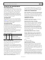
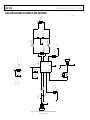
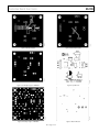
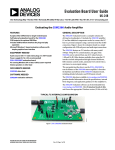
Evaluation Board User Guide
UG-196
One Technology Way • P.O. Box 9106 • Norwood, MA 02062-9106, U.S.A. • Tel: 781.329.4700 • Fax: 781.461.3113 • www.analog.com
Evaluation Board for SSM2375 Filterless Class-D Audio Amplifier
enables a low EMI mode, which significantly reduces the
radiated emissions at the Class-D outputs, particularly above
100 MHz. With this option selected, the SSM2375 can pass
FCC Class B radiated emissions testing with a 50 cm unshielded
speaker cable without any external filtering.
PACKAGE CONTENTS
EVAL-SSM2375Z evaluation board
OTHER SUPPORTING DOCUMENTATION
SSM2375 data sheet
GENERAL DESCRIPTION
The SSM2375 is a fully integrated, high efficiency, Class-D
audio amplifier. It is designed to maximize performance for
mobile phone applications. The application circuit requires a
minimum of external components and operates from a single
2.5 V to 5.5 V supply. It is capable of delivering 3 W of continuous
output power with less than 1% THD + N driving a 3 Ω load
from a 5.0 V supply.
EVALUATION BOARD OVERVIEW
The SSM2375 evaluation board carries a complete application
circuit for driving a loudspeaker. Figure 1 shows the top view of
the evaluation board, and Figure 2 shows the bottom view.
09393-002
09393-001
Spread spectrum pulse density modulation (PDM) is used to
provide lower EMI-radiated emissions compared with other
Class-D architectures. The inherent randomized nature of
spread spectrum PDM eliminates clock intermodulation
(beating effect) of several amplifiers in close proximity. The
SSM2375 includes an optional modulation select pin that
The device also includes a flexible gain select pin that only
requires one series resistor to select among 0 dB, 3 dB, 6 dB,
9 dB, or 12 dB. The benefit of this is to improve gain matching
between multiple SSM2375 devices within a single application
as compared to using external resistors to set gain. This user
guide describes how to configure and use the SSM2375 evaluation
board. It is recommended that this user guide be read in conjunction with the SSM2375 data sheet, which provides specifications,
internal block diagrams, and application guidance for the
amplifier IC.
Figure 2. SSM2375 Evaluation Board Bottom View
Figure 1. SSM2375 Evaluation Board Top View
PLEASE SEE THE LAST PAGE FOR AN IMPORTANT
WARNING AND LEGAL TERMS AND CONDITIONS.
Rev. 0 | Page 1 of 8
UG-196
Evaluation Board User Guide
TABLE OF CONTENTS
Package Contents.............................................................................. 1 Output Configuration...................................................................3 Other Supporting Documentation................................................. 1 Power Supply Configuration .......................................................3 General Description ......................................................................... 1 Component Selection ...................................................................3 Evaluation Board Overview ............................................................ 1 Getting Started...................................................................................5 Revision History ............................................................................... 2 What to Test ...................................................................................5 Setting Up the Evaluation Board .................................................... 3 Evaluation Board Schematic and Artwork.....................................6 Input Configuration ..................................................................... 3 Ordering Information.......................................................................8 Shutdown Mode............................................................................ 3 Bill of Materials..............................................................................8 Gain Configuration ...................................................................... 3 REVISION HISTORY
4/11—Revision 0: Initial Version
Rev. 0 | Page 2 of 8
Evaluation Board User Guide
UG-196
SETTING UP THE EVALUATION BOARD
INPUT CONFIGURATION
A 4-pin header (H2) on the middle left side of the board feeds
the audio signal into the board (see Figure 1). If the input audio
signal is differential (IN+ and IN−), three pins of H2 are used
for IN+, IN−, and signal ground. For a single-ended audio
input, only two pins of H2 are used. One is for the signal
ground and the other is for either IN+ or IN−. If IN+ is used,
place a jumper between Pin 3 and Pin 4 of H2, shorting IN−
to ground. If IN− is used, place the jumper between Pin 1 and
Pin 2 of H2, connecting IN+ to ground.
For optimal THD and SNR performance as specified in the
SSM2375 data sheet, remove the entire EMI filter, short across
the ferrite bead terminals, and open the capacitor terminals.
POWER SUPPLY CONFIGURATION
The 2-pin header, H1, is used to power the board. Care must be
taken to connect the dc power with correct polarity and voltage.
Reverse polarity or overvoltage may damage the board permanently. The maximum supply current is approximately 0.33 A
when driving an 8 Ω load and when the input voltage is 5 V. Do
not allow VDD to exceed 5.5 V.
SHUTDOWN MODE
COMPONENT SELECTION
The 2-pin header, J1, is used to turn on and off the SSM2375
amplifier. Placing a jumper across Pin 1 and Pin 2 of H1 puts
the SSM2375 in normal operation. Removing the jumper shuts
down the SSM2375 so that only a minimum current (about
20 nA) is drawn from the power supply.
Selecting the proper components is the key to achieving the
performance required at the cost budgeted.
GAIN CONFIGURATION
Two headers, H3 and J3, control the SSM2375 analog gain. By
placing a jumper across two pins of H3, the amplifier’s gain pin can
be connected to GND or VDD. Three jumper settings are used:
between the center pin and the left pin (HI), between the center pin
and the right pin (LO), and no jumper (open).
Placing a jumper on J3 removes the 47 kΩ resistor (R3) between
the gain pin and H3. Gain settings between 0 dB and 12 dB are
available; see Table 1 for configuration details.
J3
Short
Short
Short
Open
Open
H3
LO
Open
HI
LO
HI
If the desired gain must be adjusted beyond the available gain
settings (see the Gain Configuration section), a series resistor
can be placed in the input signal path. This creates a voltage
divider with the 80 kΩ input resistance on each input pin,
allowing an arbitrary reduction of the input signal. Note that
input signal attenuation directly reduces SNR performance;
therefore, large values compared to the built-in input resistance
should be avoided. These components are populated with 0 Ω
values on the evaluation board.
Input Coupling Capacitor Selection—C1 and C2
The input coupling capacitors, C1 and C2, should be large
enough to couple the low frequency signal components in the
incoming signal but small enough to reject unnecessary
extremely low frequency signals. For music signals, the cutoff
frequency is typically between 20 Hz and 30 Hz. The value of
the input capacitor is calculated by
Table 1. Gain Configuration
Gain
0 dB
3 dB
6 dB
9 dB
12 dB
Input Gain Resistor Selection—R1 and R2
Configuration
Short gain pin to GND
Gain pin unconnected
Short gain pin to VDD
Gain pin through 47 kΩ to GND
Gain pin through 47 kΩ to VDD
C = 1/(2πRIN fc)
where:
RIN = 80 kΩ + (R1 or R2).
fc is the desired cutoff frequency.
OUTPUT CONFIGURATION
The output connector, H4, is located on the right side of the
board (see Figure 1). H4 can drive a loudspeaker whose
impedance should be no less than 3 Ω.
Output Ferrite Beads—B1 and B2
Because the SSM2375 does not typically require any external LC
output filters due to a low noise modulation scheme, no output
filter is installed on the evaluation board. In this case, thick wire
connects the empty pads of B1 and B2, and the capacitor pads
are left unpopulated.
If the speaker length exceeds 10 cm, place Ferrite Bead B1 and
Ferrite Bead B2 in the output paths, and use Capacitors C6 and
C7 to couple the output terminals to ground, as shown in the
schematic in Figure 3. Some recommended ferrite beads are
listed in Table 2. Some users may want to use inductors for
applications with specific EMI vs. audio performance constraints; see Table 3 for recommendations.
The output beads, B1 and B2, are necessary components for
filtering out the EMI caused at the switching output nodes
when the length of the speaker wire is greater than 10 cm. The
penalty for using ferrite beads for EMI filtering is slightly worse
noise and distortion performance at the system level due to the
nonlinearity of the beads.
Ensure that these beads have enough current conducting capability
while providing sufficient EMI attenuation. The current rating
needed for an 8 Ω load is approximately 420 mA, and impedance
at 100 MHz should be ≥120 Ω. In addition, the lower the dc
resistance (DCR) of these beads, the better for minimizing their
power consumption. Table 2 describes the recommended beads.
Rev. 0 | Page 3 of 8
UG-196
Evaluation Board User Guide
Output Shunting Capacitors
Output Inductors
There are two output-shunting capacitors, C6 and C7, that work
with the ferrite beads, B1 and B2. Use small size (0603 or 0402),
multilayer ceramic capacitors made of X7R or C0G (NP0)
materials. Note that the capacitors can be used in pairs: a
capacitor with small capacitance (up to 100 pF) plus a capacitor
with a larger capacitance (less than 1 nF). This configuration
provides thorough EMI reduction for the entire frequency
spectrum. If the bill of materials must be minimized, a single
capacitor of approximately 470 pF can be used with acceptable
performance in many cases.
If inductors are preferred for EMI filtering at the output nodes,
choose components with an inductance of less than 2.2 μH.
The higher the inductance, the lower the EMI is at the output;
however, cost and power consumption are higher. Using 0.47 μH
to 2.2 μH inductors is recommended, and the current rating (and
saturation current) should exceed 600 mA for an 8 Ω load.
Table 3 shows the recommended inductors.
Table 2. Recommended Output Beads
Part No.
BLM18PG121SN1D
MPZ1608S101A
MPZ1608S221A
BLM18EG221SN1D
Manufacturer
Murata
TDK
TDK
Murata
Z (Ω)
120
100
220
220
IMAX (mA)
2000
3000
2000
2000
DCR (Ω)
0.05
0.03
0.05
0.05
Size (mm)
1.6 × 0.8 × 0.8
1.6 × 0.8 × 0.8
1.6 × 0.8 × 0.8
1.6 × 0.8 × 0.8
L (μH)
0.47
1.0
0.47
1.0
2.2
IMAX (mA)
1400
1200
1100
800
790
DCR (Ω)
0.07
0.12
0.12
0.19
0.1
Size (mm)
3.2 × 1.6 × 0.85
3.2 × 1.6 × 0.85
2.0 × 1.25 × 0.5
2.0 × 1.25 × 0.5
3.2 × 2.5 × 1.55
Table 3. Recommended Output Inductors
Part No.
LQM31PNR47M00
LQM31PN1R0M00
LQM21PNR47MC0
LQM21PN1R0MC0
LQH32CN2R2M53
Manufacturer
Murata
Murata
Murata
Murata
Murata
Rev. 0 | Page 4 of 8
Evaluation Board User Guide
UG-196
GETTING STARTED
To ensure proper operation, carefully follow Step 1 through Step 5.
WHAT TO TEST
1.
•
2.
3.
4.
5.
Place a jumper between Pin 1 and Pin 2 of J1 to enable the
amplifier.
For most audio quality testing, the EMI filtering (B1/B2
and C6/C7) must be removed. Short across the B1 and B2
terminals to make a direct connection from device output
to the H5 speaker header.
Connect the load to the audio output connector, H5.
Connect the audio input to the board in either differential
mode or single-ended mode, depending on the application.
Connect the power supply with the proper polarity and
voltage.
•
•
•
•
•
Rev. 0 | Page 5 of 8
Electromagnetic interference (EMI)—connect wires for
the speakers, making sure they are the same length as the
wires required for the actual application environment; then
complete the EMI test.
Signal-to-noise ratio.
Output noise—make sure to use an A-weighted filter to
filter the output before reading the measurement meter.
Maximum output power.
Distortion.
Efficiency.
Rev. 0 | Page 6 of 8
HDR1X4
1
2
3
4
H2
VDD
ACTIVE
C2
0.22uF
R1
R2
0
J1
HDR1X2
0
+
C5
A3
A2
A1
B1
Figure 3. Schematic of the SSM2375 Evaluation Board
47k
R3
J3
HDR1X2
C4
10uF
CAP POL
VDD
GAIN
SD
IN-
IN+
C3
0.1uF
VDD
EDGE
OUT-
OUT+
U1
SSM2375
1
2
3
HDR1X3
600103
H3
B2
B3
C3
POWER HEADER
H1
HDR1X2
C2
VDD
VDD
GND
C1
C1
0.22uF
22uF Alum.
Elec
throughole,
near H1
(nopop)
J2
HDR1X2
H4
HDR1X2
NO POP
0-ohm
VDD
B2
MPZ1608S221A
0-ohm
short
short
B1
MPZ1608S221A
NOPOP
C7 NOPOP
510pF
C6
510pF
OUT-
OUT+
H5
HDR1X2
UG-196
Evaluation Board User Guide
EVALUATION BOARD SCHEMATIC AND ARTWORK
09393-003
UG-196
09393-007
09393-004
Evaluation Board User Guide
Figure 4. Top Layer Copper
09393-008
09393-005
Figure 7. Bottom Layer Copper
Figure 8. Top Silkscreen
09393-009
09393-006
Figure 5. Second Layer Copper—GND Plane
Figure 6. Third Layer Copper—VDD Plane
Figure 9. Bottom Silkscreen
Rev. 0 | Page 7 of 8
UG-196
Evaluation Board User Guide
ORDERING INFORMATION
BILL OF MATERIALS
Table 4.
Qty
1
2
1
1
1
2
2
2
1
6
1
1
Reference Designator
U1
C1, C2
C3
C4
C5
C6, C7
B1, B2
R1, R2
R3
H1, H4, H5, J1 to J3
H2
H3
Description
IC, SSM2375
Capacitor, 22 nF, 25 V, 10%, X7R, 0805
Capacitor, ceramic 0.1 μF, 50 V, Y5V, 0603
Capacitor, ceramic 10 μF, 10 V, X5R, 0805
Capacitor, 47 μF, 25 V electrolytic
Capacitor, ceramic, 510 pF, 50 V, 2%, 0603
Wire short
Resistor, 0.0 Ω, 1/8 W, 0805
Resistor, 47 kΩ, 1/10 W, 1%, 0603
Connector, header, 2-position, 0.100" single gold
Connector, header, 4-position, 0.100" single gold
Connector, header, 3-position, 0.100" single gold
Supplier/Part No.
Analog Devices/SSM2375CBZ
Panasonic/ECJ-2YB1E224K
Panasonic/ECJ-1VF1H104Z
Murata/GRM21BR61A106KE19L
Nichicon/UFW1E470MDD
Murata/GRM1885C1H511JA01D
N/A
Panasonic/P0.0ATR-ND
Panasonic/ERJ-3EKF4702V
Tyco/826629-2
Tyco/826629-3
Tyco/826629-4
ESD Caution
ESD (electrostatic discharge) sensitive device. Charged devices and circuit boards can discharge without detection. Although this product features patented or proprietary protection
circuitry, damage may occur on devices subjected to high energy ESD. Therefore, proper ESD precautions should be taken to avoid performance degradation or loss of functionality.
Legal Terms and Conditions
By using the evaluation board discussed herein (together with any tools, components documentation or support materials, the “Evaluation Board”), you are agreeing to be bound by the terms and conditions
set forth below (“Agreement”) unless you have purchased the Evaluation Board, in which case the Analog Devices Standard Terms and Conditions of Sale shall govern. Do not use the Evaluation Board until you
have read and agreed to the Agreement. Your use of the Evaluation Board shall signify your acceptance of the Agreement. This Agreement is made by and between you (“Customer”) and Analog Devices, Inc.
(“ADI”), with its principal place of business at One Technology Way, Norwood, MA 02062, USA. Subject to the terms and conditions of the Agreement, ADI hereby grants to Customer a free, limited, personal,
temporary, non-exclusive, non-sublicensable, non-transferable license to use the Evaluation Board FOR EVALUATION PURPOSES ONLY. Customer understands and agrees that the Evaluation Board is provided
for the sole and exclusive purpose referenced above, and agrees not to use the Evaluation Board for any other purpose. Furthermore, the license granted is expressly made subject to the following additional
limitations: Customer shall not (i) rent, lease, display, sell, transfer, assign, sublicense, or distribute the Evaluation Board; and (ii) permit any Third Party to access the Evaluation Board. As used herein, the term
“Third Party” includes any entity other than ADI, Customer, their employees, affiliates and in-house consultants. The Evaluation Board is NOT sold to Customer; all rights not expressly granted herein, including
ownership of the Evaluation Board, are reserved by ADI. CONFIDENTIALITY. This Agreement and the Evaluation Board shall all be considered the confidential and proprietary information of ADI. Customer may
not disclose or transfer any portion of the Evaluation Board to any other party for any reason. Upon discontinuation of use of the Evaluation Board or termination of this Agreement, Customer agrees to
promptly return the Evaluation Board to ADI. ADDITIONAL RESTRICTIONS. Customer may not disassemble, decompile or reverse engineer chips on the Evaluation Board. Customer shall inform ADI of any
occurred damages or any modifications or alterations it makes to the Evaluation Board, including but not limited to soldering or any other activity that affects the material content of the Evaluation Board.
Modifications to the Evaluation Board must comply with applicable law, including but not limited to the RoHS Directive. TERMINATION. ADI may terminate this Agreement at any time upon giving written notice
to Customer. Customer agrees to return to ADI the Evaluation Board at that time. LIMITATION OF LIABILITY. THE EVALUATION BOARD PROVIDED HEREUNDER IS PROVIDED “AS IS” AND ADI MAKES NO
WARRANTIES OR REPRESENTATIONS OF ANY KIND WITH RESPECT TO IT. ADI SPECIFICALLY DISCLAIMS ANY REPRESENTATIONS, ENDORSEMENTS, GUARANTEES, OR WARRANTIES, EXPRESS OR IMPLIED, RELATED
TO THE EVALUATION BOARD INCLUDING, BUT NOT LIMITED TO, THE IMPLIED WARRANTY OF MERCHANTABILITY, TITLE, FITNESS FOR A PARTICULAR PURPOSE OR NONINFRINGEMENT OF INTELLECTUAL
PROPERTY RIGHTS. IN NO EVENT WILL ADI AND ITS LICENSORS BE LIABLE FOR ANY INCIDENTAL, SPECIAL, INDIRECT, OR CONSEQUENTIAL DAMAGES RESULTING FROM CUSTOMER’S POSSESSION OR USE OF
THE EVALUATION BOARD, INCLUDING BUT NOT LIMITED TO LOST PROFITS, DELAY COSTS, LABOR COSTS OR LOSS OF GOODWILL. ADI’S TOTAL LIABILITY FROM ANY AND ALL CAUSES SHALL BE LIMITED TO THE
AMOUNT OF ONE HUNDRED US DOLLARS ($100.00). EXPORT. Customer agrees that it will not directly or indirectly export the Evaluation Board to another country, and that it will comply with all applicable
United States federal laws and regulations relating to exports. GOVERNING LAW. This Agreement shall be governed by and construed in accordance with the substantive laws of the Commonwealth of
Massachusetts (excluding conflict of law rules). Any legal action regarding this Agreement will be heard in the state or federal courts having jurisdiction in Suffolk County, Massachusetts, and Customer hereby
submits to the personal jurisdiction and venue of such courts. The United Nations Convention on Contracts for the International Sale of Goods shall not apply to this Agreement and is expressly disclaimed.
©2011 Analog Devices, Inc. All rights reserved. Trademarks and
registered trademarks are the property of their respective owners.
UG09393-0-4/11(0)
Rev. 0 | Page 8 of 8