1
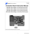
Dec. 19, 2007
Rev - 1.0
CMC
National Semiconductor
Evaluation Board User's Guide
DAC121C08XEB, DAC101C08XEB, DAC081C08XEB
Micro Power Digital-to-Analog Converter (DAC)
with an I2C-Compatible Interface
12-bit
10-bit
8-bit
DAC121C085/
DAC121C081
DAC101C085/
DAC101C081
DAC081C085/
DAC081C081
1
http://www.national.com
Table of Contents
1.0 Introduction ........................................................................................................... 3
2.0 Board Assembly.................................................................................................... 4
3.0 Quick Start ............................................................................................................ 4
3.1 Stand-Alone Mode..................................................................................... 4
3.2 Computer Mode......................................................................................... 5
4.0 Functional Description........................................................................................... 6
4.1 Jumper Settings ........................................................................................ 6
4.2 I2C Interface .............................................................................................. 6
4.3 DAC Reference Circuitry ........................................................................... 6
4.4 Analog Output ........................................................................................... 7
4.5 Power Supply Connections........................................................................ 7
5.0 Software Operation and Settings .......................................................................... 8
6.0 Evaluation Board Specifications............................................................................ 9
7.0 Hardware Schematic............................................................................................. 10
8.0 Evaluation Board Bill of Materials.......................................................................... 11
A1.0 Summary Tables of Test Points, Jumpers, and Connectors ............................... 12
2
http://www.national.com
In the Computer mode, data capture and
evaluation is simplified by connecting this board to
National Semiconductor’s Data Capture Board
(order number WAVEVSN BRD 4.4). The Data
Capture (WV4) Board is connected to a personal
computer running WaveVision software through a
USB port. The WaveVision4 software runs on
Microsoft Windows, and the latest version can be
downloaded
from
the
web
at
http://www.national.com/adc.
1.0 Introduction
The DAC121C08XEB Design Kit (consisting of the
DAC Evaluation Board and this User's Guide) is
designed
to
ease
evaluation
and
design-in
of
National
Semiconductor’s
DAC121C081/DAC121C085 family of Digital-toAnalog Converters (DACs). The Micro-Power
2
DACs feature Rail-to-Rail Output and an I CCompatible interface. This User’s Guide supports
all three resolutions of the DAC family. The
evaluation board comes with the full-featured
MSOP-8 version of the DAC. For the 12-bit
resolution, the DAC121C085 is used. For the 10bit resolution, the DAC101C085 is used. For the
8-bit resolution, the DAC081C085 is used. All the
devices
in
the
family
(DAC121C085,
DAC101C085, and DAC081C085) will be referred
to as the DAC121C085 in this document.
Note: WaveVision Software version 4.4 or later is
required to evaluate this part with the WV4
Evaluation System.
The WaveVision software allows the user to drive
the DAC121C085 with a variety of preset
waveforms and custom waveforms. The software
2
also allows the user to configure the I C serial
Interface.
The evaluation board can be used in either of two
modes. In the Stand-Alone mode, suitable test
equipment, such as a pattern generator and signal
analyzer, can be used with the board to evaluate
the DAC121C085 performance.
JP10
3P3V Select
JP5
Add Select
Data transmitted to the DAC121C085, via the
2
I C interface, is converted to an analog waveform
by U1, the DAC121C085.
JP4
Output Load
J4
VOUT
JP7
VREF Select
J1
WV4S
Connector
J2
VA Input
J3
WV4 Connector
JP9
VA Select
U1
DAC121C085
Figure 1: Component and Test Point Locations
3
http://www.national.com
2.0 Board Assembly
The DAC121C08XEB evaluation board comes
fully assembled and ready for use. Refer to the Bill
of Materials for a description of components, to
Figure 1 for major component placement, and to
Figure 12 for the Evaluation Board schematic.
14
13
12
11
10
8
SCL
3.0 Quick Start
SDA
The evaluation board may be used in the StandAlone mode or Computer mode. In Stand-Alone
mode, a Pattern Generator is used to interface to
2
the DAC’s I C Interface. In Computer Mode, a
2
WaveVision4 Board is used to drive the DAC’s I C
interface. In either case, a Signal Analyzer is used
to evaluate the analog output signal.
9
7
6
5
4
3
2
1
J3
WV4
Figure 2: J3 (WV4) Interface Header
6. The Analog Output signal can be seen DC
coupled at J5, or AC coupled at SMA
connector J4. See the board schematic of
Figure 12 for details.
7. Select the desired output load by adding
jumpers to JP4. Connect a jumper across the
two left pins near the “C” to add a 200pF load
capacitance to ground. Connect a jumper
across the two right side pins near the “R” to
add a 2kΩ resistive load. See Table 1 for
jumper configurations.
2
8. The DAC121C085 will respond to I C address
0x0C by default with pins A0 and A1 floating.
2
Change the I C slave address of the DAC by
adding jumpers to JP5. A0 is controlled by
pins 1,2, & 3 of JP5. A1 is controlled by pins
5, 6, & 7. Refer to Table 1 for a detailed
2
description of the I C Slave address settings.
NOTE: Jumper Setting changes to the pinconfigurable slave address will not take effect
until the DAC is power-cycled.
3.1 Stand-Alone Mode
Refer to Figure 1 for locations of test points and
major components.
1. Connect a clean analog (not switching) +5V
power source to Power Connector J2 on the
DAC121C08XEB board. Ground the middle
terminal and connect +5V to the bottom
terminal closest to JP9.
2. Make
the
following
required
jumper
connections, see Table 1 for more details:
• JP9 - pins 2 & 3
• JP7 - pins 2 & 3
• JP6 - pins 1 & 2
• JP8 - pins 1 & 2
3. Turn on the power source.
2
4. Configure a pattern generator or other I C
master
device
to
interface
to
the
DAC121C085. Refer to the timing diagrams
in the datasheet for further timing details. The
2
DAC supports any of the three standard I C
2
speed ranges. Ensure the I C master device
is configured to drive 5V CMOS logic.
2
5. Connect the I C master device to Serial
Interface Header J3 (WV4). Refer to Figure 2
below for connection details. NOTE: The
board comes with pull-up resistors (R6 and
2
R7). Any other pull-ups on the I C bus must
be disabled.
4
http://www.national.com
3.2 Computer Mode
Refer to Figure 1 for locations of test points and
major components. The board comes configured
for “plug-and-play” WaveVision evaluation.
13
SDA
1. Run the WaveVision 4 program, version 4.4 or
higher is required to interface to the WV4
board. While the program is loading, continue
below.
2. Connect a USB cable between the WV4 board
and the PC running the WaveVision 4
software.
3. Make
the
following
required
jumper
connections, see Table 1 for more details:
•
•
•
•
+5V
+3.3V
(EEPROM)
14
11
12
9
10
7
8
5
6
3
4
1
2
SCL
(EEPROM)
N/C
N/C
GND
SCL
(DAC)
GND
JP9 - pins 1 & 2
JP7 - pins 2 & 3
JP6 - pins 1 & 2
JP8 - pins 1 & 2
SDA
(DAC)
J1
WV4S
• JP10 - pins 1 & 2
4. Connect
the
J1
header
on
the
DAC121C08XEB evaluation board to the WV4
serial connector (J7) on the WV4 board.
Refer to Figure 3 for the serial connection and
Figure 4 for the J1 header pin out.
Note: J1 on the DAC121C08XEB is
intentionally stuffed on the bottom side of the
board.
Figure 4: J1 (WV4S) Header
5. Perform step 7 of section 3.1 to configure the
loading of the analog output (VOUT).
6. Perform step 8 of section 3.1 to configure the
2
I C slave address of the DAC.
7. Connect a clean (not switching) +5.0V power
source with a 350mA current limit to power
connector J1 on the WV4 board. Turn on the
power supply.
8. Refer to Section 5.0 on Software Operation
and Settings to setup the WaveVision 4
software.
Figure 3: WV4 to DAC121C08XEB Connection
5
http://www.national.com
2
4.2 I C Interface
4.0 Functional Description
2
The DAC supports all three I C speeds, including
Hs-Mode (3.4MHz). In Hs-Mode the maximum
DAC conversion rate is 188.9kHz. The board is
2
designed with 1kΩ I C pull-up resistors on both
the SDA and SCL lines (R6 & R7). Also, series
resistors for SCL and SDA are designed into the
board (R8 & R9). The board is shipped with 51Ω
series resistors which can be increased to
2
interface to a noisy I C bus.
4.1 Jumper Settings
Table 1 describes the function of the various
jumpers on the DAC121C08XEB evaluation
board. The evaluation board schematic is shown
in Figure 12.
Pins 1 & 2
Pins 2 & 3
Jumper
2
JP4
VOUT Load Select (See Below)
JP5
I C Address Select (See Below)
JP6
Enable VREF supply to the DAC.
In Computer Mode, the I C interface is driven by
the WaveVision4 board.
The WaveVision4
software allows the user to drive the DAC121C085
with various digitized signals. Refer to Section 5.0
“Software Operation and Settings” for further
information.
2
2
Use external
VREF from J2.
JP7
JP8
In Stand-Alone Mode, the I C interface must be
driven by an external device. See section 1.4.5 of
the DAC121C081/DAC121C085 datasheet for a
typical write sequence timing diagram.
Set VREF = VA
Enable VA supply to the DAC.
JP9
Use VA from the
WV4 board
Use external VA
from J2.
JP10
Use 3.3V supply
from the WV4
board
Use external
3.3V supply from
TP6.
2
The maximum digital input level of the I C
interface depends on the analog supply voltage
(VA). The interface operates at normal CMOS
logic levels. See the Electrical Characteristics
section of the datasheet for further details.
The SDA signal is accessible by connecting to
pin 2 of the WV4 connector (J3). The SCL signal
is accessible by connecting to pin 6 of J3.
Jumper JP4 (VOUT Load Select)
Left side
pins near
“C”
Connect a 200pF load capacitance
from VOUT to GND
Please refer to section 1.4 of the datasheet for a
2
detailed description of the I C interface. Refer to
the Philips I2C Specification for further details.
Right side
pins near
“R”
Connect a 2kΩ load resistance from
VOUT to GND
4.3 DAC Reference Circuitry
The reference voltage for the DAC121C085 is
selected by JP7. (See Table 1 for details.) The
reference can either be selected as the VA supply
or an externally supplied voltage (J2). The analog
output range of the DAC121C085 can be scaled
by adjusting the reference voltage (VREF). The
lower the VREF, the smaller the output range. VREF
can be set anywhere from 1.0V to VA. VA is
independent of VREF and can be set anywhere
from +2.7V to +5.5V. In any case, VREF has little
to no PSRR and must be as clean as possible to
reduce noise feedthrough on VOUT.
2
Address
Jumper JP5 (I C Address Select)
0x0C
No jumpers
0x0D
Short pins 2 & 3.
0x0E
Short pins 1 & 2.
0x08
Short pins 6 & 7.
0x09
Short pins 2 & 3 and pins 6 & 7.
0x0A
Short pins 1 & 2 and pins 6 & 7.
0x4C
Short pins 5 & 6.
0x4D
Short pins 2 & 3 and pins 5 & 6.
0x4E
Short pins 1 & 2 and pins 5 & 6.
Table 1: Jumper Configurations
6
http://www.national.com
If you wish to supply VA externally, connect a DC
voltage supply to connector J2. Connect GND to
the center terminal and VA to the bottom terminal.
Place a jumper across pins 2 and 3 of JP9 to
select VA_REMOTE. This voltage (VA) can be set
anywhere from +2.7V to +5.5V. The source of
VREF is controlled by the JP7 jumper. To set
VREF=VA, short pins 2 & 3. To use an external
VREF from the top terminal of J2, short pins 1 & 2.
Refer to Figure 6 for a diagram of the power
supply connections.
4.4 Analog Output
The analog output of this Eval board is available in
two places. For a DC coupled output, pin 1 of J5
provides VOUT and pin 2 provides AGND. An AC
coupled output is provided by the SMA connector
(J4). See Figure 5 below for details.
If using a spectrum analyzer to look at the output
of the DAC, the AC coupled output (J4) is
recommended.
For very low frequency (i.e. less than 1kHz), use
J5 to see the output signal DC coupled. For an
AC coupled output at low frequencies, simply
replace the AC coupling capacitor at C9 with a
larger capacitor. Use the J4 SMA to look at the
AC coupled output.
AC Coupled
VOUT
VREF
AGND
VOUT
VA
Figure 6: Power Supply Connections
Figure 5: Analog Output
Typical supply currents when applying an external
supply to VA and VREF are as follows:
4.5 Power Supply Connections
• For VA = +3.3V, I = 7mA
• For VA = +5.0V, I = 12mA
In Computer mode, the board can be powered by
either an external supply or the local WaveVision4
board supply.
In Stand-alone mode, the
Evaluation Board must be powered by an external
supply.
Note: These values are specified for a
continuously operating DAC in High Speed Mode,
driving a full-scale sinewave output. The majority
of this current is for powering devices external to
the DAC121C085 such as the pull-up resistors
and the LED.
If you wish to use the local supply from the
WaveVision4 Board, place a jumper across pins 1
and 2 of JP9. This connection will supply +5V to
VA on the DAC board. To set VREF=VA, simply
short pins 2 & 3 of JP7. For WaveVision to
recognize the board, the 3P3V supply must be
enabled as well. Do this by placing a jumper
across pins 1 and 2 of JP10. The board comes
configured to use the local supply. The default
jumper settings are shown in Figure 1.
7
http://www.national.com
Remote
2
7. Configure the I C address of the DAC. The
2
DAC121C085 will respond to I C address
0x0C by default with pins A0 and A1 floating
2
(no jumpers on JP5). Change the I C slave
address of the DAC by adding jumpers to JP5.
Refer to Table 1 for a detailed description of
2
the I C address settings. The address in
Figure 8 must match the address configured
by A0 and A1.
NOTE: Jumper Setting changes to the pinconfigured slave address will not take effect
until the DAC is power-cycled.
5.0 Software Operation and Settings
The WaveVision4 software is included with the
WaveVision4 board and the latest version can be
downloaded from National's web site at
WaveVision4
http://www.national.com/adc.
software version 4.4 or later is required to evaluate
this device with the WV4 system.
To install this software, follow the procedure in the
WaveVision4 Board User's Guide. Once the
software is installed, run it and set it up as follows:
Note: Before continuing, ensure that the
WaveVision Hardware is setup according to
Section 3.2.
1. From the WaveVision main menu, go to
Settings, then Capture Settings to open the
System Settings dialog.
2. Under board type, select WaveVision4 (USB).
2
Figure 8: I C Address
3. Turn on the power to both boards, then click
on the "Reset" button and await the firmware
download.
After the firmware has
downloaded, WaveVision will open up a
control panel window for the DAC121C08XEB.
8. Perform register level control of the DAC by
writing 16-bit words to the DAC Data Register.
To write the DAC, simply type a 16-bit hex
value into the “Manual DAC Control” field and
press Enter or click the “Write DAC Register”
button. See Figure 9.
4. Click on the "Close" button to close the
System Settings Dialog.
5. Navigate to the DAC121C08XEB Evaluation
Board window.
2
6. Configure the I C Interface speed as seen in
Figure 7. Standard mode, Fast Mode, and
High Speed mode are supported.
Figure 9: Manual DAC Control
9. To put the DAC into power-down mode, select
a power-down option from the “Power-down
Mode” box and click the “Set Mode” button.
2
Figure 7: I C Speed Select
Figure 10: DAC Power-down Control
8
http://www.national.com
10. Configure the digital waveform to be
converted by the DAC as seen in Figure 11.
Please see the WaveVision4 User’s Manual
for detailed instructions. The ability to drive
preset waveforms or custom data is provided.
6.0 Evaluation Board Specifications
Board Size:
Power Requirements
I2C Interface Speed:
Analog Output
AC Coupled
Output Range:
Impedance:
2.8" x 2.0" (7.2 cm x 5.1 cm)
Min: +2.7V , 6mA Max: +5.5V, 16mA
100 kHz, 400kHz, or 3.4 MHz
-(VA/2) to (VA/2)
User Selectable: 2KΩ, 200pF, or ∞.
Figure 11: Waveform Configuration
11. Press the “Start” button to begin driving the
digital waveform to the DAC.
The WaveVision4 Board will continuously send the
2
waveform out to the DAC over the I C interface
until the “Stop” button is pressed. Please refer to
Section 4.4 for details on measuring the Analog
Output of the DAC.
The Digital Waveform is plotted in the main
WaveVision window for added convienience. This
waveform may be further analyzed by clicking on
the magnifying glass icon, then clicking and
dragging across a specific area of the plot for
better data inspection. See the WaveVision4
Board User's Guide for details.
If this board is used in conjunction with the
WaveVision4
Data
Capture
Board
and
WaveVision software, a USB cable is needed to
connect WaveVision4 Board to the host computer.
See the WaveVision4 Board User's Guide for
details.
9
http://www.national.com
REM
WV
3P3V_WV
TP6
1
2
3
TP7
AGND
AGND
3P3V_REMOTE
3P3V
JP10
3P3V
1
3P3V
1
6
8
10
12
14
5
7
9
11
13
SCL_DUT
SCLHS_E
5
7
9
11
13
6
8
10
12
14
SCL_DUT
SCLHS_E
0.1uF
1uF
D2
RED LED
3P3V
R11
510
C8
C7
3P3V
3
SDA
1
4
8
SDA_DUT 2
3P3V_WV
J3
WV4
4
3
SDA
2
SCL
WV4
5P0V_WV
SCL
WV4S
3P3V
5
J1
WV4S
7
WP
VCC
1
A0
2
A1
6
SCL
A2
3P3V
3
GND SDA
4
SDA_DUT 1
U3
24C02
TP5
AGND
1
AGND
R6
1K
VA
VA
NS
C6
R7
1K
VA
4
51
51
R8
R9
1
2
3
4
5
6
7
VA
U2
NC7SZ126P5X_NL
VA
A1
AGND
VA
A0
AGND
1
C9
1uF
4
3
2
1
AGND
VOUT
GND
VA
VREF
VOUT
5
6
7
8
C
C2
R
C3
C5
0.1uF 1uF
C4
TP3
AGND
0.1uF
C11
0.1uF
C10
JP4
HEADER 4X2_0
2K
R1
0.1uF 1uF
1
2
AGND
2
1
VOUT
DAC121C085
SDA
SCL
A1
A0
U1
TP2
AGND
1
C1
3
4
200pF
AGND
TP4
VA
JP6
I_VREF
VA
D1
RED LED
R10
510
VA
VA
JP8
I_VA
L1
TP1
AGND
VA
1
2
3
5P0V_WV
AGND
100uH
1
3
2
4
5
JP5
ADDRESS SELECT
Y
5
VCC
OE
1
A
2
GND
3
1
2
1
2
J4
VOUT
VA
JP7
VREF
VREF=VA
VREF_EXT
JP9
VA SELECT
WV
VOUT
1
10
1
1
2
3
REM
J5
LED
1
2
3
J2
VIN
VREF
AGND
VA_REMOTE
7.0 Hardware Schematic
Figure 12: DAC121C08XEB Evaluation Board Schematic
http://www.national.com
8.0 Evaluation Board Bill of Materials
Quantity
Reference
PCB
Footprint
1
6
4
2
1
1
C1
C2,C4,C6,C8,C10,C11
C3,C5,C7,C9
D1,D2
JP4
JP5
rc0603
rc0603
c1206
D1206-21
hdr2x2
hdr1x7
1
1
1
1
1
1
JP6
JP7
JP8
JP9
JP10
J1
1
1
1
1
1
1
2
2
2
5
1
1
1
1
1
J2
J3
J4
J5
L1
R1
R6,R7
R10,R11
R8,R9
TP1,TP2,TP3,TP5,TP7
TP4
TP6
U1
U2
U3
hdr1x2
hdr1x3
hdr1x2
hdr1x3
hdr1x3
hdr2x7_2mmrh
ED120-3
berg2x7p
SMA
hdr1x2
1206
rc0603
rc0603
rc0603
rc0603
tp_60c40dp
tp_60c40dp
tp_60c40dp
mso8SD-8
sc70-5
so8
Source
Source Part #
Rating
10V
10V
10V
Digikey
516-1440-1-ND
Digikey
S1011E-36-ND
Digikey
Digikey
Digikey
Digikey
Digikey
Digikey
S1011E-36-ND
S1011E-36-ND
S1011E-36-ND
S1011E-36-ND
S1011E-36-ND
S5803-21-ND
Digikey
Digikey
ED1609-ND
A26529-40-ND
Digikey
Digikey
S1011E-36-ND
445-1543-1-ND
Digikey
Digikey
Digikey
S1011E-36-ND
S1011E-36-ND
S1011E-36-ND
11
Value
200pF
0.1uF
1uF
RED LED
HEADER 4X2_0
ADDRESS
SELECT
I_VREF
VREF
I_VA
VA SELECT
3P3V
WV4S
VIN
WV4
VOUT
LED
100uH
2K
1K
510
51
AGND
VA
3P3V_REMOTE
DAC121C085
NS
24C02
http://www.national.com
APPENDIX
A1.0 Summary Tables of Test Points, Jumpers, and Connectors
Test Points on the DAC121C08XEB Evaluation Board
TP1: AGND
Ground. Located at the top center of the board.
TP2: AGND
Ground. Located at the top center of the board.
TP3: AGND
Ground. Located at the bottom right of the board.
TP4: VA
VA Test Point. Located at the bottom right of the board.
TP5: AGND
Ground. Located at the top left of the board.
TP6: 3P3V
3.3V test point. Located at the top left of the board.
TP7: AGND
Ground. Located at the bottom left of the board.
Connectors on the DAC121C08XEB Evaluation Board
J1: WV4S Header
Wave Vision 4 Serial connector. Stuffed on the bottom side of the board intentionally.
J2: Terminal Block
VREF, AGND, VA_REMOTE. External power supply connector.
J3: Serial Interface
Header
Serial Interface header. Logic Input. (Refer to Figure 2 for a pin-out diagram.)
J4: SMA Connector
VOUT_AC. AC Coupled Analog Output.
J5: 2-pin Header
VOUT. DC Coupled Analog Output.
Selection Jumpers on the DAC121C08XEB Evaluation Board (Refer to Table 1 in Section 4.0 for configuration details)
JP4: VOUT Load Select
Configures the load on VOUT. Refer to Table 1.
JP5: I2C Address
Select
Configures the DAC’s I2C address. Refer to Table 1. Note: Changes to the pin-configured I2C slave
address do not take effect until the DAC is power-cycled.
JP6: I_VREF
Enables VREF supply to the DAC. Also used to measure isolated VREF current.
JP7: VREF Select
Selects the VREF source. VREF is either supplied externally or connected to VA by this jumper.
JP8: I_VA
Enables VA supply to the DAC. Also used to measure isolated VA current.
JP9: VA Select
Selects the VREF source. VREF is either supplied externally or connected to VA by this jumper.
JP10: 3P3V Select
Selects the 3.3V source for powering the WaveVision EEPROM (U3). Always set to pins 1 and 2 for
WaveVision operation.
12
http://www.national.com
[Blank Page]
13
http://www.national.com
BY USING THIS PRODUCT, YOU ARE AGREEING TO BE BOUND BY THE TERMS AND CONDITIONS OF NATIONAL
SEMICONDUCTOR'S END USER LICENSE AGREEMENT. DO NOT USE THIS PRODUCT UNTIL YOU HAVE READ AND
AGREED TO THE TERMS AND CONDITIONS OF THAT AGREEMENT. IF YOU DO NOT AGREE WITH THEM, CONTACT THE
VENDOR WITHIN TEN (10) DAYS OF RECEIPT FOR INSTRUCTIONS ON RETURN OF THE UNUSED PRODUCT FOR A
REFUND OF THE PURCHASE PRICE PAID, IF ANY.
The DAC121C08XEB, DAC101C08XEB, & DAC081C08XEB Evaluation Boards are intended for product evaluation purposes only
and are not intended for resale to end consumers, are not authorized for such use and are not designed for compliance with
European EMC Directive 89/336/EEC, or for compliance with any other electromagnetic compatibility requirements.
National Semiconductor Corporation does not assume any responsibility for use of any circuitry or software supplied or described.
No circuit patent licenses are implied.
LIFE SUPPORT POLICY
NATIONAL'S PRODUCTS ARE NOT AUTHORIZED FOR USE AS CRITICAL COMPONENTS IN LIFE SUPPORT DEVICES OR
SYSTEMS WITHOUT THE EXPRESS WRITTEN APPROVAL OF THE PRESIDENT OF NATIONAL SEMICONDUCTOR
CORPORATION. As used herein:
1. Life support devices or systems are devices or systems
which, (a) are intended for surgical implant into the body,
or (b) support or sustain life, and whose failure to
perform, when properly used in accordance with
instructions for use provided in the labeling, can be
reasonably expected to result in a significant injury to the
user.
National Semiconductor Corporation
Americas
Tel:
1-800-272-9959
Fax: 1-800-737-7018
Email: [email protected]
2. A critical component is any component in a life support
device or system whose failure to perform can be
reasonably expected to cause the failure of the life
support device or system, or to affect its safety or
effectiveness.
National Semiconductor Europe
Fax: +49 (0) 1 80-530 85 86
Email: [email protected]
Deutsch Tel: +49 (0) 699508 6208
English Tel: +49 (0) 870 24 0 2171
Français Tel: +49 (0) 141 91 8790
National Semiconductor
Asia Pacific Customer
Response Group
Tel: 65-2544466
Fax: 65-2504466
Email:[email protected]
National
Semiconductor
Japan Ltd.
Tel: 81-3-5639-7560
Fax: 81-3-5639-7507
www.national.com
National does not assume any responsibility for any circuitry described, no circuit patent licenses are implied and National reserves the right at any time
without notice to change said circuitry and specifications.
14
http://www.national.com
IMPORTANT NOTICE
Texas Instruments Incorporated and its subsidiaries (TI) reserve the right to make corrections, modifications, enhancements, improvements,
and other changes to its products and services at any time and to discontinue any product or service without notice. Customers should
obtain the latest relevant information before placing orders and should verify that such information is current and complete. All products are
sold subject to TI’s terms and conditions of sale supplied at the time of order acknowledgment.
TI warrants performance of its hardware products to the specifications applicable at the time of sale in accordance with TI’s standard
warranty. Testing and other quality control techniques are used to the extent TI deems necessary to support this warranty. Except where
mandated by government requirements, testing of all parameters of each product is not necessarily performed.
TI assumes no liability for applications assistance or customer product design. Customers are responsible for their products and
applications using TI components. To minimize the risks associated with customer products and applications, customers should provide
adequate design and operating safeguards.
TI does not warrant or represent that any license, either express or implied, is granted under any TI patent right, copyright, mask work right,
or other TI intellectual property right relating to any combination, machine, or process in which TI products or services are used. Information
published by TI regarding third-party products or services does not constitute a license from TI to use such products or services or a
warranty or endorsement thereof. Use of such information may require a license from a third party under the patents or other intellectual
property of the third party, or a license from TI under the patents or other intellectual property of TI.
Reproduction of TI information in TI data books or data sheets is permissible only if reproduction is without alteration and is accompanied
by all associated warranties, conditions, limitations, and notices. Reproduction of this information with alteration is an unfair and deceptive
business practice. TI is not responsible or liable for such altered documentation. Information of third parties may be subject to additional
restrictions.
Resale of TI products or services with statements different from or beyond the parameters stated by TI for that product or service voids all
express and any implied warranties for the associated TI product or service and is an unfair and deceptive business practice. TI is not
responsible or liable for any such statements.
TI products are not authorized for use in safety-critical applications (such as life support) where a failure of the TI product would reasonably
be expected to cause severe personal injury or death, unless officers of the parties have executed an agreement specifically governing
such use. Buyers represent that they have all necessary expertise in the safety and regulatory ramifications of their applications, and
acknowledge and agree that they are solely responsible for all legal, regulatory and safety-related requirements concerning their products
and any use of TI products in such safety-critical applications, notwithstanding any applications-related information or support that may be
provided by TI. Further, Buyers must fully indemnify TI and its representatives against any damages arising out of the use of TI products in
such safety-critical applications.
TI products are neither designed nor intended for use in military/aerospace applications or environments unless the TI products are
specifically designated by TI as military-grade or "enhanced plastic." Only products designated by TI as military-grade meet military
specifications. Buyers acknowledge and agree that any such use of TI products which TI has not designated as military-grade is solely at
the Buyer's risk, and that they are solely responsible for compliance with all legal and regulatory requirements in connection with such use.
TI products are neither designed nor intended for use in automotive applications or environments unless the specific TI products are
designated by TI as compliant with ISO/TS 16949 requirements. Buyers acknowledge and agree that, if they use any non-designated
products in automotive applications, TI will not be responsible for any failure to meet such requirements.
Following are URLs where you can obtain information on other Texas Instruments products and application solutions:
Products
Applications
Audio
www.ti.com/audio
Automotive and Transportation www.ti.com/automotive
Amplifiers
amplifier.ti.com
Communications and Telecom www.ti.com/communications
Data Converters
dataconverter.ti.com
Computers and Peripherals
www.ti.com/computers
DLP® Products
www.dlp.com
Consumer Electronics
www.ti.com/consumer-apps
DSP
dsp.ti.com
Energy and Lighting
www.ti.com/energy
Clocks and Timers
www.ti.com/clocks
Industrial
www.ti.com/industrial
Interface
interface.ti.com
Medical
www.ti.com/medical
Logic
logic.ti.com
Security
www.ti.com/security
Power Mgmt
power.ti.com
Space, Avionics and Defense
www.ti.com/space-avionics-defense
Microcontrollers
microcontroller.ti.com
Video and Imaging
www.ti.com/video
RFID
www.ti-rfid.com
OMAP Mobile Processors
www.ti.com/omap
Wireless Connectivity
www.ti.com/wirelessconnectivity
TI E2E Community Home Page
e2e.ti.com
Mailing Address: Texas Instruments, Post Office Box 655303, Dallas, Texas 75265
Copyright © 2012, Texas Instruments Incorporated