1
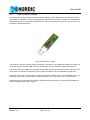
Remote Control Reference Design
nRD24H1
User Guide
All rights reserved.
Reproduction in whole or in part is prohibited without the prior written permission of the copyright holder.
December 2006
User Guide
Liability disclaimer
Nordic Semiconductor ASA reserves the right to make changes without further notice to the product to
improve reliability, function or design. Nordic Semiconductor ASA does not assume any liability arising out
of the application or use of any product or circuits described herein.
Life support applications
These products are not designed for use in life support appliances, devices, or systems where malfunction
of these products can reasonably be expected to result in personal injury. Nordic Semiconductor ASA customers using or selling these products for use in such applications do so at their own risk and agree to fully
indemnify Nordic Semiconductor ASA for any damages resulting from such improper use or sale.
Contact details
For your nearest dealer, please see http://www.nordicsemi.no
Receive available updates automatically by subscribing to eNews from our homepage or check our website regularly for any available updates.
Main office:
Otto Nielsen’s vei 12
7004 Trondheim
Phone: +47 72 89 89 00
Fax: +47 72 89 89 89
www.nordicsemi.no
Revision History
Date
December 2006
Revision 1.0
Version
1.0
Page 2 of 21
Description
Remote Control Reference Design
Contents
1
2
3
3.1
3.1.1
3.2
3.3
3.3.1
3.4
4
4.1
4.2
4.3
5
5.1
5.2
5.3
5.4
5.5
5.6
5.7
Introduction ................................................................................................. 4
System Overview ........................................................................................ 4
Hardware Description.................................................................................. 6
RF Module............................................................................................ 6
Specifications ................................................................................... 8
Application Board ................................................................................. 8
USB Receive Dongle ........................................................................... 10
Specifications ................................................................................... 11
nRF24L01 Samples ............................................................................. 11
Hardware Design Guidelines ...................................................................... 12
RF Module............................................................................................ 12
Application Board ................................................................................. 12
USB Receive Dongle ........................................................................... 13
Appendix ..................................................................................................... 14
Bill Of Materials (BOM) ........................................................................ 14
Application board schematics .............................................................. 16
USB receive dongle schematics .......................................................... 17
RF module schematics......................................................................... 18
Design layout for application board ...................................................... 19
Design layout for USB receive dongle ................................................. 20
Design layout for the RF module.......................................................... 21
Revision 1.0
Page 3 of 21
User Guide
1
Introduction
nRD24H1 is a reference design for the nRF24L01 general purpose radio chip. The purpose of this document is to help with the design of RF based remote controls operating in the worldwide 2.4GHz ISM band.
Based on this reference design you will be able to design one-way and two-way remote controls that are
not limited by line-of-sight conditions. This reference design also provides valuable design suggestions for
other applications with comparable data rates.
2
System Overview
The reference design consists of complete design files (schematics, layout, Gerber, BOM data and source
code) for a USB receive dongle, an RF module and, an application board. The remote control unit consists
of the RF module and application board. The RF module contains all critical parts and the application
board is easily redesigned for the form factor of the finished product.
MCU
MOSI
MISO
SCK
CSN
nRF24L01
CE
INT
Buttons or
GP I/O
Figure 1. Block diagram of the remote control unit
The USB receive dongle may be used as-is with no hardware changes. The USB receive dongle and
remote control unit are not supplied with plastic housing.
USB
MCU
MOSI
MISO
SCK
CSN
nRF24L01
CE
INT
Figure 2. Block diagram of the USB receive dongle
You can download the design files from Nordic Semiconductor at www.nordicsemi.no.
Revision 1.0
Page 4 of 21
Remote Control Reference Design
It is assumed that the USB receive dongle is permanently on while the PC it is plugged into is on. The USB
receive dongle goes to a low power mode when the PC is in standby. Only the remote control unit is optimized for long battery life.
Revision 1.0
Page 5 of 21
User Guide
3
Hardware Description
This section describes the hardware units that are supplied with the nRD24H1.
3.1
RF Module
In most applications, redesigning the RF module is not required. The RF module includes the nRF24L01
radio IC and all its supporting components, that is, antenna, matching network and crystal. The RF module
also contains a microcontroller. The circumference of the RF module holds GPIO pins of the MCU. The
choice of pins enables the RF module to support several different IO standards:
•
•
•
•
14 pins for matrix scan of 49 keyboard buttons + 1 LED output.
SPI master interface + 14 GPIO pins.
Two GPIO pins may alternatively be used for a 2-wire interface (master or slave).
Two GPIO pins may alternatively be used for a UART interface.
Figure 3. RF module
The nRF24L01 radio IC uses a differential antenna interface for both receive and transmit. Connected to
this interface are a balun (balanced/unbalanced) and a matching network.
The nRF24L01 needs very few external components. A resistor is used for biasing while two small capacitors are sufficient for decoupling. The nRF24L01 also needs an external 16MHz crystal for time reference.
The radio is tolerant of ±60ppm crystals, but the RF module is equipped with a ±10ppm crystal because
this is the most common tolerance for a crystal of this size.
The Atmel ATmega88 MCU is rich in hardware IO features while consuming little power. The MCU on the
RF module is programmed from a header on the Application board. The MCU has a 4kbyte program memory and an internal RC oscillator running on 1MHz. Tools from Atmel are necessary to reprogram the MCU.
Revision 1.0
Page 6 of 21
Remote Control Reference Design
Pin
1
2
3
4
5
6
7
8
9
10
11
12
13
14
15
16
17
18
19
20
21
22
23
24
Name
GND
PD7
PC0
PC1
PC4
PC5
PB4
PB5
GND
PC2
PB3
VCC
PC6
PD0
PD1
GND
PC3
PD3
PD4
PB6
PD5
PD6
PB2
GND
Alternate function
LED2
RX data
VOL - / SDA
VOL UP / SCL
MISO
SCK
MOSI
RESET
TX data
STOP
PLAY
FORWARD
BACK
LED1
Table 1. RF module pinout
Note: The PB2 pin of the Atmel ATmega88 MCU has special functionality. This pin may not be used
as a general purpose input pin in the current design. We recomend that you limit its use to
one of the following:
• Not connected (as is the case with the present Application Board)
• General-purpose output pin for a LED etc.
• SPI slave select for devices on your custom Application Board
• SPI slave select for the MCU in case devices on your custom Application Board need this
communication mode with the MCU.
For more information, please consult the Atmel datasheet.
The RF module has an operating range from 1.9 to 3.6V.
Revision 1.0
Page 7 of 21
User Guide
3.1.1
Specifications
Operating conditions
Supply voltage
Current consumption
Status
Range
1.9 - 3.6 V
20µA with brownout detection at 3 V supply.
1.2µA without brownout detection.
15 mA peak at 3 V supply
2402-2478 MHz
0 dBm
Idle
Peak current
Radio frequency
Output power
Table 2. Electrical Specifications
PCB type
PCB dimension
Length x width x height
1.6 mm 2 layer FR4
39 mm x 17 mm x 1.6 mm
Table 3. Physical Specifications
3.2
Application Board
While the RF module can be used as-is in a vast number of applications, the application board is made
with redesign in mind. It is hard to anticipate all the different form factors that end products based on
nRD24H1 may have. But, the most likely hardware differences will be in casing, button placement, display
design and power management. We have not considered the casing design at all, but the rest of the application board should be very easy to redesign.
The Application board that ships with nRD24H1 contains the following units:
•
•
•
•
•
•
•
Footprint for the RF module
Six buttons
Batteries
External power connector
Programming header for the MCU on the RF module
Two LEDs
Debug pins for application development
The power switch S7 can be used in conjunction with the batteries or the external power connector. You
should use either batteries or external power. External power on (batteries off) is selected with the switch
pointing down while batteries on (external power off) is selected with the switch pointing up.
Note: It is important to keep the voltage supply within the 1.9 to 3.6V limits. There is no over voltage
protection circuitry on the Application board.
P1 is the ISP6PIN connector used to reprogram Atmel MCUs and has the standard Atmel 6-pin ISP pinout.
P2 contains the GPIO pins that may also work as UART and 2-wire interface. The pin names on the debug
connector P3 are according to Atmel ATmega88 IO pin names. The pins on P1 and P2 are also available
on P3.
Pin
1
2
3
Revision 1.0
Function
MISO
VCC
SCK
Page 8 of 21
Remote Control Reference Design
Pin
4
5
6
Function
MOSI
RST
GND
Table 4. ISP connector, P1
The ATmega88 can be programmed with any ISP capable programmer for the Atmel MCUs. The ISP connector, P1, has the same pin out as Atmel uses on its programmers, that is, the STK500. The programming
details are explained in the software guide.
Pin
1
2
3
4
5
6
7
8
9
10
11
12
13
14
15
16
17
18
19
20
21
22
Name
VCC
PD7
PC0
PB2
PD6
PD5
PB6
PD4
PD3
PC3
PD1
PD0
PC6
PB3
PC2
PB5
PB4
PC5
PC4
PC1
GND
GND
Alternate function
LED2
LED1
BACK
FORWARD
PLAY
STOP
TX data
RX data
RESET
MOSI
SCK
MISO
VOL UP / SCL
VOL DOWN / SDA
Table 5. P3 pinout
Pin
1
2
3
4
Name
PD0
PC5
PD1
PC4
Alternate function
RX data
SCL
TX data
SDA
Table 6. P2 pinout
Revision 1.0
Page 9 of 21
User Guide
3.3
USB Receive Dongle
The USB receive dongle should not need hardware redesign in most applications. The USB receive dongle features the nRF24L01 with the same supporting components as on the RF module. The USB interface
is provided by a Silicon Laboratories C8051F321 IC. This IC also acts as an MCU running the remote control signal reception application.
Figure 4. USB receive dongle
The nRF24L01 requires a supply voltage of between 1.9 and 3.6V. The C8051F321 features a voltage regulator that takes 5V from the USB connector and provides 3V to the rest of the USB receive dongle.
The bottom side of the USB receive dongle has one button and the top side has one LED. These two components are not important in nRD24H1 but have been included in case your application needs them.
The C8051F321 uses an internal timer for waking up the MCU when the PC is in a suspended mode. The
frequency of this timer is controlled by the value of the cap, C12, connected to pin P0.2 of the MCU.
Programming the C8051F321 is done with a ISP programmer from SiLabs. The programming details for
this are explained in the software guide.
Revision 1.0
Page 10 of 21
Remote Control Reference Design
3.3.1
Specifications
Operating conditions
Supply voltage
Current consumption
Suspend
Connected
Radio frequency
Output power
4.5 - 5.5 V
450 µA
25.5 mA
2402-2478 MHz
0 dBm
Table 7. Electrical Specifications
PCB type
PCB dimension
Length x width x height
1.6mm 2 layer FR4
42mm x 15mm x 1.6mm
Table 8. Physical Specifications
3.4
nRF24L01 Samples
The samples that are supplied with the nRD24H1 are provided so that you can easily start a design using
this part. The nRD24L01 is a general purpose radio IC operating with very low power consumption. More
information about this chip can be found on www.nordicsemi.no.
Revision 1.0
Page 11 of 21
User Guide
4
Hardware Design Guidelines
This chapter describes important issues that might affect you when developing the remote control reference design for a finished product.
4.1
RF Module
The RF module is designed to cover most remote control and keyboard applications. The most likely
change to the RF module is that the antenna may need some retuning for your finished application. The
form factor of the Application board in the end product may influence the radiation pattern.
The matching network for the nRF24L01 has the same layout as in the reference design from the
datasheet with only some small component changes to compensate for the smaller PCB. The 50 ohm reference point will be between C5 and C14, where C14 is used to match the antenna to this 50 ohm impedance.
Note: Changing the thickness of the PCB will require a retuning of the antenna matching network.
In a mass produced product it is likely that the components on the RF module will be merged with the rest
of the electronics. Also, the component cost may be optimized depending on your volumes and needs. In
such cases, we recommend that you use the design files for the RF module and keep the RF portion of the
design. This includes:
•
•
•
•
4.2
The nRF24L01 radio and its decoupling.
The antenna matching network.
The ground plane pattern between the radio and the antenna.
The ground vias.
Application Board
As stated above, the application board is made with redesign in mind and you can redesign it for your product with minimal effort.
We have identified three likely scenarios:
1.
2.
3.
For demonstrators, a one-off application board can be combined with the RF modules sold in the
nRD24H1 box.
For low to mid quantity production, you may produce the RF module yourself and mount it on
your custom application board.
For high quantity production, merging the electronics on the Application board and RF module
will cut production cost.
For the first two scenarios the modified application board must contain the following basic features in addition to your choice of buttons and display:
•
•
•
The U-shaped footprint for the RF module with all the IO pads placed on the nRD24H1 Application
board.
A voltage supply to the RF module in the range between 1.9 to 3.6V.
A programming header for the Atmel AVR MCU on the RF module.
Revision 1.0
Page 12 of 21
Remote Control Reference Design
4.3
USB Receive Dongle
The USB dongle contains all the components that are necessary for a finished product.
The matching network for the nRF24L01 has the same layout as in the reference design from the
datasheet with only some small component changes to compensate for the smaller PCB. The 50 ohm reference point will be between C5 and L4, where L4 is used to match the antenna to this 50 ohm impedance.
The following design alterations are likely to the USB receive dongle:
•
•
Tools from Silicon Laboratories are required to reprogram the USB receive dongle with your software. The top side of the USB receive dongle has a 4-pin programming interface for Silicon Laboratories ISP tools. The 4-pin connector will likely be omitted from the BOM of a production model.
The LED and button are placed on the the USB receive dongle. If your application does not need
these functions, it is easy to disregard the components without having to alter the PCB layout.
Note: If you need the button and/or LED and find it inconvenient that they are on the bottom side,
the simplest modification is to turn the USB connector upside down.
•
•
It is possible to reduce the size of the USB receive dongle by using a chip antenna or another
antenna configuration, choosing a more compact USB connector or, altering the layout. If you
choose to do so, the antenna matching network must be redesigned.
The antenna is matched for best reception when the dongle is placed in a USB slot of a computer,
and without a plastic housing. Adding housing can affect the antenna resulting in the antenna
matching needing changed.
Revision 1.0
Page 13 of 21
User Guide
5
5.1
Appendix
Bill Of Materials (BOM)
Part
LED Green
Header 2x6
Header 2x2
Header 2x11
Screw terminal
100R
NA
Switch
Switch
Battery
Designator
Footprint
LED1, LED2
1206
P1
Header 2x6
P2
Header 2x2
P3
Header 2x11
P4
P5
R1, R2
0402
R3, R4
0402
S1, S2, S3, S4, S5, S6SKHJAD
S7
BT1
Description
Led Green 1206
Pin Header 2x6
Pin Header 2X2
Pin Header 2x11
Phoenix MPT 0,5/2-2,54
NA
100R
NA
Alps SKHUAD
EAO, type 1K2 straigh pins
2xAAA Battery box
Figure 5. Application board BOM
Part
15pF
2.2nF
4.7pF
1.5pF
1.0pF
33nF
1nF
10nF
100nF
33pF
1uF
LED GREEN
8.2nH
2.7nH
3.9nH
USB Type A
Header 1x4
1M
22k
1k
100R
NA
ALPS SKHUAD
nRF24L01
C8051F321
16MHz
Designator
C1, C2
C3
C4
C5
C6, C14
C7
C8
C9
C10, C11
C12
C13
D1
L1
L2
L3
P1
P2
R1
R2
R3, R4
R5
R6
S1
U1
U2
X1
Footprint
0402s
0402s
0402s
0402s
0402s
0402s
0402s
0402s
0402s
0402s
0402s
1.6X0.8X0.4
0402s
0402s
0402s
USB through hole
HDR1X4
0402s
0402s
0402s
0402s
0402s
ALPS SKHUAD
QFN20L/4x4
MLP-28
TSX-4025
Description
15pF NP0 +/-2%
2.2nF X7R +/-10%
4.7pF NP0 +/-0.25pF
1.5pF NP0 +/-0.1pF
1.0pF NP0 +/-0.1pF
33nF X7R +/-10%
1nF X7R +/-10%
10nF X7R +/-10%
100nF X7R +/-10%
33pF NP0 +/-5%
1uF 6.3V X5R
LED GREEN 0603
Chip inductor, +/- 5%
Chip inductor, +/- 5%
Chip inductor, +/- 5%
Molex 47037-0001
1M 5%
22k 1%
1k 5%
100R
NA
Nordic Semiconductor
SiLabs
16MHz, CL=9pF, < +/- 60ppm
Figure 6. USB receiver dongle BOM
Revision 1.0
Page 14 of 21
Remote Control Reference Design
Part
15pF
2.2nF
4.7pF
1.5pF
1.0pF
33nF
1nF
10nF
10uF
100nF
8.2nH
2.7nH
6.8nH
1M
22k
nRF24L01
atMega88V-10MU
16MHz
Designator
C1, C2
C3
C4
C5
C6, C14
C7
C8
C9
C10
C11, C12, C13, C15
L1
L2
L3
R1
R2
U1
U2
X1
Footprint
0402
0402
0402
0402
0402
0402
0402
0402
1206
0402
0402
0402
0402
0402
0402
QFN20L/4x4
QFN32L/5x5
TSX-4025
Figure 7. RF module BOM
Revision 1.0
Page 15 of 21
Description
15pF NP0 +/-2%
2.2nF X7R +/-10%
4.7pF NP0 +/-0.25nF
1.5pF NP0 +/-0.1nF
1.0pF NP0 +/-0.1nF
33nF X7R +/-10%
1nF X7R +/-10%
10nF X7R +/-10%
10uF 6.3V Tantal
100nF X7R +/-10%
Chip inductor, +/- 5%
Chip inductor, +/- 5%
Chip inductor, +/- 5%
1M 5%
22K 1%
Nordic Semiconductor
Atmel
16MHz, CL=9pF, < +/- 60ppm
User Guide
Application board schematics
5.2
A
B
PC0
PD6
PB6
PD3
PD1
PC6/RST
PC2
PB4/MISO
PC4
2
4
6
8
10
12
14
16
18
20
22
PD7
PB2
PD5
PD4
PC3
PD0
PB3/MOSI
PB5/SCK
PC5
PC1
VCC
R1
100R
LED1
PD6
2
R4
PB3/MOSI
NA
VCC
VCC
GND
PC6/RST
PB5/SCK
PB4/MISO
PB3/MOSI
PB2
PB6
PC0
PC1
PC2
PC3
PC4
PC5
PD0
PD1
PD3
PD4
PD5
PD6
PD7
R3
3
J12
J13
J8
J7
J11
J23
J20
J3
J4
J10
J17
J5
J6
J14
J15
J18
J19
J21
J22
J2
J9
J16
J24
J1
P5
GND
BT2
2XAAA
4
VCC
BT1
S7
2XAAA
GND
4
GND
For component/bottom side
mount. Only one battery box is
connected.
GND
2
PD7
Vol+
PC5
LED2
S1
VCC
GND
SCL
SDA
PC6/RST
PB5/SCK
PB4/MISO
P1
AVR ISP
2
4
NA
PC5
PC4
To be used only as pull-ups for I2C
Title
nRD24H1-APPBOARD-A
Revision
A
Size
Sheet 1 of 1
Drawn By: KJO
Project Number
1
Date: 15.12.2006
File: nRD24H1_APPBOARD-A.SchDoc
3
3
R2
100R
S2
VolPC4
Stop
PD3
S3
S4
Forward
PB6
Play
PD4
S5
Back
PD5
1
3
P2
2
4
6
P3
1
3
5
7
9
11
13
15
17
19
21
GND
S6
RXD
TXD
1
3
5
1
VCC
GND
GND
2
P4
1
2
A
B
C
D
Page 16 of 21
Revision 1.0
C
D
1
PD1
PD0
Remote Control Reference Design
USB receive dongle schematics
5.3
A
B
C
D
1
1
P1
4
3
2
1
VDD
USB Type A
P2
1
2
3
4
GND
Programmer
GND
2
2
VDD
VDD
C10
100nF
GND
GND
3
P0.1
P0.0
GND
D+
DVDD
REGIN
C12
33pF
C13
1uF
MISO 1
SCK 2
3
4
5
6
7
GND
3
R4
1k
U2
P1.1
P1.2
P1.3
P1.4
P1.5
P1.6
P1.7
21
20
19
18
17
16
15
C8051F321
VDD
R3
1k
C11
100nF
CSN
D1
4
VDD
GND
S1
R6
NA
VDD
LED GREEN
R5
100R
4
CE
CSN
SCK
MOSI
MISO
IRQ
C7
33nF
1
2
3
4
5
CE
CSN
SCK
MOSI
MISO
VDD
5
nRF24L01
5
1M
X1
R1
C1
15pF
C9
1nF
C8
6
10nF
VDD
22k
15
14
13
12
11
R2
U1
VDD
VSS
ANT2
ANT1
VDD_PA
Nordic
16MHz
C2
15pF
Title
L1
L3
6.8nH
L2
8.2nH
2.7nH
C3
2.2nF
Project Number
C5
1.5pF
C4
4.7pF
nRD24H1-USBDONGLE-A
Size
6
Date: 15.12.2006
File: nRD24H1_USBDONGLE-A.SchDoc
7
L4
1.0nH
C6
1.0pF
7
PCB Antenna
Revision
A
Sheet 1 of 1
Drawn By: KJO
8
8
A
B
C
D
Page 17 of 21
Revision 1.0
20
19
18
17
16
VSS
DVDD
VDD
VSS
IREF
IRQ
VDD
VSS
XC2
XC1
6
7
8
9
10
MOSI
CE
IRQ
28
27
26
25
24
23
22
P0.2
P0.3
P0.4
P0.5
P0.6
P0.7
P1.0
VBUS
/RST / C2CK
P3.0 / C2D
P2.3
P2.2
P2.1
P2.0
8
9
10
11
12
13
14
User Guide
RF module schematics
5.4
1
VDD
RST
SCK
MISO
MOSI
PB2
PB6
PC0
PC1
PC2
PC3
PC5
PC4
PD7
PD6
PD5
PD4
PD3
PD1
PD0
2
VDD
C13
100nF
PC2
PC3
PC4
PC5
RST
PD0
PD1
IRQ
25
26
27
28
29
30
31
32
U2
3
C15
100nF
PC0
PC1
(ADC2) PC2
(ADC3) PC3
(ADC4) PC4
(ADC5) PC5
(RESET) PC6
(RDX) PD0
(TXD) PD1
(INT0) PD2
3
VDD
VDD
C12
100nF
16
15
14
13
12
11
10
9
atMega88V-10MU
PB4 (MISO)
PB3 (MOSI/OC2A)
PB2 (SS/OC1B)
PB1 (OC1A)
PB0 (ICP1/CLKO)
PD7 (AIN1)
PD6 (AIN0/OC0A)
PD5 (T1/OC0B)
4
4
VDD
C10
10uF
MISO
MOSI
SCK
PB2
PD7
PD6
PD5
C11
100nF
IRQ
5
5
CE
CSN
SCK
MOSI
MISO
C7
33nF
1
2
3
4
5
CE
CSN
SCK
MOSI
MISO
VDD
20
19
18
17
16
R1
C1
15pF
X1
R2
22k
1M
6
15
14
13
12
11
nRF24L01
16MHz
C2
15pF
VDD
10nF
C9
1nF
C8
L1
8.2nH
L3
6.8nH
L2
2.7nH
7
C3
2.2nF
C5
1.5pF
C4
4.7pF
A
C14
C6 1.0pF
1.0pF
Revision
Project Number
Size
7
Sheet 1 of 1
Drawn By: KJO
6
Date: 15.12.2006
File: nRD24H1_RFMODULE-A.SchDoc
nRD24H1-RFMODULE-A
Title
U1
nRF24L01 VDD
VSS
ANT2
ANT1
VDD_PA
VSS
DVDD
VDD
VSS
IREF
IRQ
VDD
VSS
XC2
XC1
A
B
J12
J13
J8
J7
J11
J23
J20
J3
J4
J10
J17
J6
J5
J2
J22
J21
J19
J18
J15
J14
J9
J16
J24
J1
2
8
PCB Antenna
8
A
B
C
D
Page 18 of 21
Revision 1.0
C
D
1
PB6
6
7
8
9
10
24
23
22
21
20
19
18
17
(ADC1) PC1
(ADC0) PC0
ADC7
GND
AREF
ADC6
AVCC
(SCK) PB5
PD3 (INT1/OC2B)
PD4 (T0/XCK)
GND
VCC
GND
VCC
PB6 (XTAL1)
PB7 (XTAL2)
1
2
3
4
5
6
7
8
PD3
PD4
Remote Control Reference Design
5.5
Design layout for application board
Figure 8. Application board top layer
Figure 9. Application board top overlay
Figure 10. Application board bottom layer
Revision 1.0
Page 19 of 21
User Guide
5.6
Design layout for USB receive dongle
Figure 11. USB receive dongle top layer
Figure 12. USB receive dongle top overlay
Figure 13. USB receive dongle bottom layer
Revision 1.0
Page 20 of 21
User Guide
5.7
Design layout for the RF module
Figure 14. RF module top layer
Figure 15. RF module top overlay
Figure 16. RF module bottom layer
Revision 1.0
Page 21 of 21