1
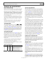
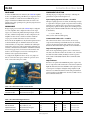
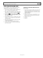
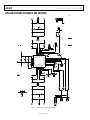
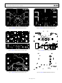
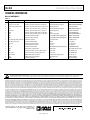
Evaluation Board User Guide
UG-360
One Technology Way • P.O. Box 9106 • Norwood, MA 02062-9106, U.S.A. • Tel: 781.329.4700 • Fax: 781.461.3113 • www.analog.com
Evaluation Board for SSM3302 2 × 10 W Filterless Class-D Stereo Audio Amplifier
PACKAGE CONTENTS
EVAL-SSM3302Z evaluation board
OTHER SUPPORTING DOCUMENTATION
SSM3302 data sheet
GENERAL DESCRIPTION
The SSM3302 is a fully integrated, high efficiency, stereo Class-D
audio amplifier. The application circuit requires a minimum of
external components and operates from a single 7 V to 18 V supply.
It is capable of delivering 2 × 8 W of continuous output power
into an 8 Ω load (or 2 × 10 W into 4 Ω) with <1% total harmonic
distortion plus noise (THD + N) from a 12 V supply. In addition,
while mono mode is active, a load as small as 2 Ω up to 20 W
continuous output power can be driven by stacking the stereo
output terminals.
Spread spectrum pulse density modulation is used to provide
lower EMI-radiated emissions compared with other Class-D
architectures. The SSM3302 includes an optional modulation select
pin (ultralow EMI emission mode) that significantly reduces the
radiated emissions at the Class-D outputs, particularly above
100 MHz. The SSM3302 can pass FCC Class-B emissions testing
with an unshielded 20 inch cable using common-mode chokebased filtering.
The fully differential input of the SSM3302 provides excellent
rejection of common-mode noise on the input. The device also
includes a highly flexible gain select pin that only requires one
series resistor to choose any of the five gain options between 9 dB
and 24 dB, with no change to the input impedance. The benefit
of this is to improve gain matching between multiple SSM3302
devices within a single application compared to using external
resistors to set gain.
This user guide describes how to configure and use the SSM3302
evaluation board. This user guide should be read in conjunction
with the SSM3302 data sheet, which provides specifications,
internal block diagrams, and application guidance for the
amplifier IC.
EVALUATION BOARD OVERVIEW
The SSM3302 evaluation board carries a complete circuit for
driving a pair of loudspeakers. Figure 1 shows the top view of
the evaluation board, and Figure 2 shows the bottom view of the
evaluation board.
Figure 1. SSM3302 Evaluation Board Top View
PLEASE SEE THE LAST PAGE FOR AN IMPORTANT
WARNING AND LEGAL TERMS AND CONDITIONS.
10399-002
10399-001
EVALUATION BOARD TOP VIEW AND BOTTOM VIEW
Figure 2. SSM3302 Evaluation Board Bottom View
Rev. 0 | Page 1 of 8
UG-360
Evaluation Board User Guide
TABLE OF CONTENTS
Package Contents.............................................................................. 1 Power Supply Configuration .......................................................3 Other Supporting Documentation................................................. 1 Analog Supply................................................................................3 General Description ......................................................................... 1 Edge Mode......................................................................................4 Evaluation Board Overview ............................................................ 1 Mono Mode....................................................................................4 Evaluation Board Top View and Bottom View............................. 1 Component Selection ...................................................................4 Revision History ............................................................................... 2 Intital Evaluation Board Setup.........................................................5 Setting Up the Evaluation Board .................................................... 3 Suggested System Level and Audio Tests ...................................5 Input Configuration ..................................................................... 3 Evaluation Board Schematic and Artwork.....................................6 Shutdown Mode............................................................................ 3 Ordering Information.......................................................................8 Gain Configuration ...................................................................... 3 Bill of Materials..............................................................................8 Output Configuration.................................................................. 3 REVISION HISTORY
2/12—Revision 0: Initial Version
Rev. 0 | Page 2 of 8
Evaluation Board User Guide
UG-360
SETTING UP THE EVALUATION BOARD
INPUT CONFIGURATION
OUTPUT CONFIGURATION
On the bottom center of the PCB are four 2-pin headers, H3 to H6.
These are used to connect the input audio signals to the amplifier.
The output terminals, J3 to J6, provide convenient attachment
points for speakers or other load devices with standard banana
connectors. In addition, 2-pin, 0.100 inch headers are provided.
Because the SSM3302 does not typically require any external audio
band LC output filtering due to a low noise modulation scheme,
a low cost, high performance, common-mode choke-based filter
is installed on the evaluation board for EMI suppression. For
optimal performance measurement, remove this filtering by
inserting 0 Ω links or a thick wire short across L1 and L2. In
this case, leave the filter capacitors, C16 to C18 and C26 to C28,
unpopulated.
If the input audio signals are differential, use the two center pins
of H3 and H4 (INL+ and INL−) for left channel audio and the two
center pins of H5 and H6 (INR+ and INR−) for the right channel
audio. In this case, connect either the top or the bottom pin to
the source/signal ground.
For single-ended audio inputs, the input lines are connected
only to the pins of H3 (INL+ and GND) and H5 (INR+ and GND).
Jumpers are placed in H4 and H6, shorting INL− and INR− to
ground.
Alternatively, single-ended stereo audio may be supplied by
connecting a standard ⅛ inch stereo plug to the J7 input
instead of connecting it to H3 and H5.
SHUTDOWN MODE
The 3-pin headers, H9 and H12, are used to tie SDNL and SDNR
to either GND or AVDD, to enable or disable the left and right
channels of the SSM3302 amplifier. Placing a jumper between
the center pin and AVDD puts the SSM3302 in normal operation.
Placing the jumper between the center pin and GND shuts down
the SSM3302 so that only a minimum current (about 10 μA)
is drawn from the power supply.
GAIN CONFIGURATION
Two headers, H2 and JP6, control the SSM3302 analog gain. By
placing a jumper across the two pins of H2, the GAIN pin of
the amplifier can be connected to GND or AVDD. Three jumper
settings are used: between the center pin and the top pin (AVDD),
between the center pin and the bottom pin (GND), and no
jumper (open).
A 47 kΩ resistor, R18, is inserted between the GAIN pin and
the H2 jumper. Placing a jumper on JP6 shorts across this
resistor (R18), allowing two extra gain levels.
Gain settings between 9 dB and 24 dB are available. See Table 1
for the gain configuration details.
Table 1. Gain Configuration
Gain (dB)
9
12
15
18
24
JP6
Short
Open
Open
Open
Short
H2
GND
GND
Open
AVDD
AVDD
Configuration
Short GAIN pin to GND
GAIN pin through 47 kΩ to GND
GAIN pin unconnected
GAIN pin through 47 kΩ to AVDD
Short GAIN pin to AVDD
To safeguard against system radiated emission failure, especially
if the speaker cable length exceeds 20 cm, it may be necessary to
include an output filter. The recommended filter uses commonmode chokes, L1 and L2, in the output paths, plus capacitors,
C16 to C18 and C26 to C28, to couple the output terminals to
ground. A schematic of this configuration is shown in Figure 4,
with recommended values for the filter components given. The
recommended common-mode chokes are listed in Table 2.
Alternatively, inductors may be used instead of common-mode
chokes; however, the distortion performance is slightly worse at
high power. If inductors are used, they must be used in pairs,
with two inductors replacing each common-mode choke. A
summary of the recommended inductors is shown in Table 3.
For optimal total harmonic distortion (THD) and signal-to-noise
ratio (SNR) performance as specified in the SSM3302 data sheet,
remove the output filters and short across L1 and L2.
POWER SUPPLY CONFIGURATION
The banana jacks, J1 and J2, are used to power the board. Care
must be taken to connect the dc power with correct polarity and
voltage. Reverse polarity or overvoltage may damage the board
permanently. Permissible supply voltages range from 7 V to 18 V;
higher voltages may damage the amplifier.
ANALOG SUPPLY
In addition to the 7 V to 18 V power supply, a 5 V analog supply
(AVDD) must be present to power the input stage and modulator.
The SSM3302 amplifier has an internal regulator to provide a
clean 5 V rail for this purpose; alternatively, an external supply
can be used.
When the REGEN pin is pulled high (between 1.35 V and 5.5 V),
the internal regulator is enabled, and the chip begins to operate.
If the REGEN pin is pulled low, the regulator is enabled, and an
external supply must be connected to H1. Do not connect the
REGEN pin directly to PVDD, because this will damage the
regulator.
On the SSM3302 evaluation board, the voltage drop from the
power indicator LED, D2, is used to provide the logic high level
for REGEN. To enable the regulator, tie the center pin of JP3 to
the upper pin, V_LED. To disable the regulator, tie it to GND.
Rev. 0 | Page 3 of 8
UG-360
Evaluation Board User Guide
EDGE MODE
COMPONENT SELECTION
To reduce the EMI emissions emitted by the SSM3302 amplifier
at the cost of slightly lower peak efficiency, an edge rate control
mode is available. To enable the reduced-EMI mode, place a
jumper on H10 between EDGE and AVDD. To return to the
ordinary (fast-edge) operating mode, place the jumper between
EDGE and GND.
Selecting the proper components is the key to achieving the
performance required at the budgeted cost.
Input Coupling Capacitor Selection—C1 and C2
The input coupling capacitors, C1 and C2, should be large enough
to couple the low frequency signal components in the incoming
signal; however, small enough to reject unnecessary extremely
low frequency signals. For music signals, the cutoff frequency is
typically between 20 Hz and 30 Hz. The value of the input capacitor
is calculated by
MONO MODE
If larger output power is needed, the SSM3302 may be configured
as a mono amplifier. This configuration allows both output
stages to be connected in parallel, allowing for larger currents
and, thus, smaller load impedances. In this configuration, the
amplifier can drive loads as small as 2 Ω with a maximum
output power of 20 W without the need for a heat sink.
C = 1/(2π × 40 kΩ × fC)
where fC is the desired cutoff frequency.
Common Mode Choke Coils—L1 and L2
The common-mode choke coils, L1 and L2, are necessary
components for filtering out the EMI caused at the switching
output nodes when the length of the speaker wire is greater
than 20 cm. Recommended components are shown in Table 2.
In mono mode, the amplifier uses only the audio signal connected
to the left channel input. To minimize distortion and other
undesired effects, it is important to minimize the cable length
between the output stages. The recommended configuration is
as follows: connect the load to the OUTL+ and OUTL− terminals,
and use heavy gage wire to short between the terminals of L1
and L2 as shown in Figure 3, instead of connecting the two
channels at the output banana terminals.
Output Shunting Capacitors
There are six output shunting capacitors, C16 to C18 and C26 to
C28, that work with the common-mode chokes coils, L1 and L2.
Use small size (0603 or 0402), multilayer ceramic capacitors
made of X7R or C0G (NP0) materials. The recommended value
is 1000 pF.
To configure the amplifier for mono mode, use a jumper on
H11 to connect the center pin to AVDD. To operate in stereo
mode, connect the center pin to GND.
Output Inductors
10399-003
If inductors are preferred for EMI filtering at the output nodes,
choose components with an inductance of less than 2.2 μH. The
higher the inductance, the lower the EMI is at the output; however,
cost and power consumption are higher. Using 1.0 μH to 2.2 μH
inductors is recommended, and the current rating (and saturation
current) should exceed 2000 mA for an 8 Ω load. Table 3 shows
the recommended inductors.
Figure 3. Board Modifications for Mono Mode
Table 2. Recommended Common-Mode Chokes
Part No.1
DLW5BTN251SQ2
DLW5BTN101SQ2
1
Manufacturer
Murata Manufacturing Co.
Murata Manufacturing Co.
Z (Ω at 100 MHz)
250
100
IMAX (mA)
5000
6000
DCR (Ω)
0.014
0.009
Size (mm)
5.0 × 5.0 × 2.35
5.0 × 5.0 × 2.35
L (μH)
1.0
1.0
1.0
1.5
IMAX (mA)
2450
2400
2300
2000
DCR (Ω)
0.087
0.052
0.054
0.105
Size (mm)
2.5 × 2.0 × 1.2
3.2 × 2.5 × 1.7
3.2 × 2.5 × 1.55
2.5 × 2.0 × 1.2
Contact Murata Manufacturing Co. for further options.
Table 3. Recommended Output Inductors
Part No.
VLS252012ET-1R0N
BRL3225T1R0M
LQH32PN1R0NN0L
VLS252012ET-1R5N
Manufacturer
TDK Corporation
Taiyo Yuden, Co., Ltd
Murata Manufacturing Co.
TDK Corporation
Rev. 0 | Page 4 of 8
Evaluation Board User Guide
UG-360
INTITAL EVALUATION BOARD SETUP
To get the amplifier to work in a simple single-ended stereo
configuration for quick evaluation, follow these steps:
SUGGESTED SYSTEM LEVEL AND AUDIO TESTS
1.
•
2.
3.
4.
5.
6.
7.
8.
Test the following:
Ensure that the output filter is installed or 0 Ω links are in
place to connect the output terminals to the IC.
Place a jumper between the upper two pins of JP3 (on the
right, next to the power LED) to enable the internal regulator.
In the bottom right corner, place jumpers from SDNL to
AVDD, from SDNR to AVDD, and from MONO to GND.
Choose a gain setting by following the instructions in the
Gain Configuration section.
In the bottom left corner, choose an EDGE setting. Verify
that H1 does not have a jumper because this would short
the internal regulator.
Place jumpers on H4 and H6, and connect a stereo audio
source to the ⅛ inch jack, J7.
Connect speakers to the left and right banana jacks.
Connect a power supply to the PVDD and GND banana
jacks on the top edge.
•
•
•
•
•
Rev. 0 | Page 5 of 8
Electromagnetic interference (EMI). Connect wires for the
speakers, ensuring that they are the same length as the wires
required for the actual application environment, and then
complete the EMI test.
Signal-to-noise ratio.
Output noise. Ensure that an A-weighted filter is used to
filter the output before reading the measurement meter.
Maximum output power.
Distortion.
Efficiency.
Rev. 0 | Page 6 of 8
1
2
J4
2
Figure 4. Schematic of the SSM3302 Evaluation Board
H6
H5
H4
H3
PHONEJACK STEREO
J7
1
3
H13
1
2
1
2
1
2
1
2
C17
1000PF
SPKG
C16
1000PF
1
2
C18
1000PF
1UF
C8
1UF
1UF
C7
C6
1UF
C5
C9
0.1UF
250OHMS
L1
2
3
H10
H9
0.22UF
1
2
3
1
2
3
AVDD
AVDD
USE 35V OR 50V
C11
0.22UF
USE 35V OR 50V
C10
TP1
BLK
AVDD
C3
1UF
BOOTL_POS
OUTL_POS
OUTL_POS
OUTL_NEG
OUTL_NEG
BOOTL_NEG
AGND
VREG_AVDD
SDNL_N
EDGE
H11
1
2
3
4
5
OUTL6
BTL7
8
9
C30 SDNL10
2.2UF
EDGE
BTL+
OUTL+
SPKG
J1
PVDD
1
P
PVDD
1UF
C4
10UF
C2
470UF
C1
N
PAD
40
39
38
37
36
35
34
33
32
31
1
1
2
3
AVDD
R6
4.99K
R7
4.99K
4.99K
R5
1
BOOTR_POS
OUTR_POS
OUTR_POS
OUTR_NEG
OUTR_NEG
BOOTR_NEG
AGND
REGEN_N
SDNR_N
GAIN
C
A
AVDD
2
30
29
28
27
26
25
24
23
22
21
D1
REGENSDNRGAIN
OUTRBTR-
BTR+
OUTR+
SSM3302
U1
PGND
J2
1
H1
1
4
AVDD
D2
R19
10K
PVDD
C
A
TP3
1
1
2
3
GND
V_LED
REGEN
TP4
AVDD
1
2
3
JP3
0.22UF
USE 35V OR 50V
C21
0.22UF
USE 35V OR 50V
C20
1
4
250OHMS
L2
1
TP2
H12
MOLEX22-28-4033
1
J3
1
1
3
1
2
PAD
PGND
PGND
PGND
PVDD
PVDD
PVDD
PVDD
PGND
PGND
PGND
INL_POS
INL_NEG
NC
SCK
SDA
MONO
THERM
NC
INR_NEG
INR_POS
INL+ 11
INL- 12
13
14
SCK
15
SDA
MONO 16
THERM 17
18
19
20
INRINR+
47K
R18
JP6
2
AVDD
C28
1000PF
1
2
3
H2
C27
1000PF
SPKG
C26
1000PF
J5
J6
1
1
2
H14
SDA
SCK
1
2
3
4
5
6
7
8
9
10
USBI
USBI FOR SDA + SCL
1
EXTERNAL VREG SUPPLY
UG-360
Evaluation Board User Guide
EVALUATION BOARD SCHEMATIC AND ARTWORK
10399-004
Figure 8. SSM3302 Evaluation Board Bottom Layer Copper
Figure 6. SSM3302 Evaluation Board Second Layer Copper
10399-009
10399-006
Figure 5. SSM3302 Evaluation Board Top Layer Copper
10399-008
UG-360
10399-005
Evaluation Board User Guide
10399-007
10399-010
Figure 9. SSM3302 Evaluation Board Top Silkscreen
Figure 7. SSM3302 Evaluation Board Third Layer Copper
Figure 10. SSM3302 Evaluation Board Bottom Silkscreen
Rev. 0 | Page 7 of 8
UG-360
Evaluation Board User Guide
ORDERING INFORMATION
BILL OF MATERIALS
Table 4.
Qty
1
4
6
1
6
1
1
1
1
8
6
6
1
2
1
1
3
4
1
1
Reference Designator
C1
C10, C11, C20, C21
C16 to C18, C26 to C28
C2
C3 to C8
C30
C9
D1
D2
H1, H3 to H6, H13, H14, JP6
H2, H9 to H12, JP3
J1 to J6
J7
L1, L2
R18
R19
R5 to R7
TP1 to TP4
U1
USBI
Description
Electrolytic, 470 μF, 16 V
Ceramic capacitor, X7R, 0603, 0.22 μF, 50 V
Ceramic capacitor, X7R, 0603, 1000 pF, 200 V
Ceramic capacitor, X5R, 1206, 10 μF, 25 V
Ceramic capacitor, X7R, 1210, 1 μF, 50 V
Ceramic capacitor, X7R, 1206, 2.2 μF, 25 V
Ceramic capacitor, X7R, 1206, 0.1 μF, 50 V
LED yellow surface mount
LED blue surface mount
Breakaway header
3-position PCB header
Banana jack uninsulated
3.5 mm audio jack stereo
Common-mode choke
Resistor film, 1206, 47 kΩ
Resistor thick film, 1206, 10 kΩ, 0.25 W
Resistor thick film, 1206, 4.99 kΩ, 1%
CONN-PCB, test point, black
SSM3302 Class-D amplifier
10-pin box header
Supplier
Panasonic
Murata Manufacturing Co.
AVX Corporation
Murata Manufacturing Co.
AVX Corporation
TDK
Phycomp (Yageo)
Chicago Miniature Lighting, LCC
Chicago Miniature Lighting, LCC
Tyco Electronics
Molex
Johnson
Cui, Inc.
Murata Manufacturing Company
Multicomp
Panasonic
Panasonic
Components Corporation
Analog Devices
3M
Part No.
EEUFM1C471
GCM188R71H224KA64D
06032C102JAT2A
GRM31CR61E106KA12L
12105C105KAT2A
C3216X7R1E225K
CC1206KRX7R9BB104
CMD67-21UYC/TR8
CMD67-21UBC/TR8
9-146285-0-02
22-28-4033
108-0740-001
SJ1-3523N
DLW5BTN251SQ2L
MC 0.125W 1206 1% 47K
ERJ-8ENF1002V
ERJ-8ENF4991V
TP-104-01-00
SSM3302ACPZ
N2510-6002RB
ESD Caution
ESD (electrostatic discharge) sensitive device. Charged devices and circuit boards can discharge without detection. Although this product features patented or proprietary protection
circuitry, damage may occur on devices subjected to high energy ESD. Therefore, proper ESD precautions should be taken to avoid performance degradation or loss of functionality.
Legal Terms and Conditions
By using the evaluation board discussed herein (together with any tools, components documentation or support materials, the “Evaluation Board”), you are agreeing to be bound by the terms and conditions
set forth below (“Agreement”) unless you have purchased the Evaluation Board, in which case the Analog Devices Standard Terms and Conditions of Sale shall govern. Do not use the Evaluation Board until you
have read and agreed to the Agreement. Your use of the Evaluation Board shall signify your acceptance of the Agreement. This Agreement is made by and between you (“Customer”) and Analog Devices, Inc.
(“ADI”), with its principal place of business at One Technology Way, Norwood, MA 02062, USA. Subject to the terms and conditions of the Agreement, ADI hereby grants to Customer a free, limited, personal,
temporary, non-exclusive, non-sublicensable, non-transferable license to use the Evaluation Board FOR EVALUATION PURPOSES ONLY. Customer understands and agrees that the Evaluation Board is provided
for the sole and exclusive purpose referenced above, and agrees not to use the Evaluation Board for any other purpose. Furthermore, the license granted is expressly made subject to the following additional
limitations: Customer shall not (i) rent, lease, display, sell, transfer, assign, sublicense, or distribute the Evaluation Board; and (ii) permit any Third Party to access the Evaluation Board. As used herein, the term
“Third Party” includes any entity other than ADI, Customer, their employees, affiliates and in-house consultants. The Evaluation Board is NOT sold to Customer; all rights not expressly granted herein, including
ownership of the Evaluation Board, are reserved by ADI. CONFIDENTIALITY. This Agreement and the Evaluation Board shall all be considered the confidential and proprietary information of ADI. Customer may
not disclose or transfer any portion of the Evaluation Board to any other party for any reason. Upon discontinuation of use of the Evaluation Board or termination of this Agreement, Customer agrees to
promptly return the Evaluation Board to ADI. ADDITIONAL RESTRICTIONS. Customer may not disassemble, decompile or reverse engineer chips on the Evaluation Board. Customer shall inform ADI of any
occurred damages or any modifications or alterations it makes to the Evaluation Board, including but not limited to soldering or any other activity that affects the material content of the Evaluation Board.
Modifications to the Evaluation Board must comply with applicable law, including but not limited to the RoHS Directive. TERMINATION. ADI may terminate this Agreement at any time upon giving written notice
to Customer. Customer agrees to return to ADI the Evaluation Board at that time. LIMITATION OF LIABILITY. THE EVALUATION BOARD PROVIDED HEREUNDER IS PROVIDED “AS IS” AND ADI MAKES NO
WARRANTIES OR REPRESENTATIONS OF ANY KIND WITH RESPECT TO IT. ADI SPECIFICALLY DISCLAIMS ANY REPRESENTATIONS, ENDORSEMENTS, GUARANTEES, OR WARRANTIES, EXPRESS OR IMPLIED, RELATED
TO THE EVALUATION BOARD INCLUDING, BUT NOT LIMITED TO, THE IMPLIED WARRANTY OF MERCHANTABILITY, TITLE, FITNESS FOR A PARTICULAR PURPOSE OR NONINFRINGEMENT OF INTELLECTUAL
PROPERTY RIGHTS. IN NO EVENT WILL ADI AND ITS LICENSORS BE LIABLE FOR ANY INCIDENTAL, SPECIAL, INDIRECT, OR CONSEQUENTIAL DAMAGES RESULTING FROM CUSTOMER’S POSSESSION OR USE OF
THE EVALUATION BOARD, INCLUDING BUT NOT LIMITED TO LOST PROFITS, DELAY COSTS, LABOR COSTS OR LOSS OF GOODWILL. ADI’S TOTAL LIABILITY FROM ANY AND ALL CAUSES SHALL BE LIMITED TO THE
AMOUNT OF ONE HUNDRED US DOLLARS ($100.00). EXPORT. Customer agrees that it will not directly or indirectly export the Evaluation Board to another country, and that it will comply with all applicable
United States federal laws and regulations relating to exports. GOVERNING LAW. This Agreement shall be governed by and construed in accordance with the substantive laws of the Commonwealth of
Massachusetts (excluding conflict of law rules). Any legal action regarding this Agreement will be heard in the state or federal courts having jurisdiction in Suffolk County, Massachusetts, and Customer hereby
submits to the personal jurisdiction and venue of such courts. The United Nations Convention on Contracts for the International Sale of Goods shall not apply to this Agreement and is expressly disclaimed.
©2012 Analog Devices, Inc. All rights reserved. Trademarks and
registered trademarks are the property of their respective owners.
UG10399-0-2/12(0)
Rev. 0 | Page 8 of 8