1
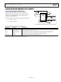
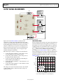
ADP223/ADP225 User Guide
UG-227
One Technology Way • P.O. Box 9106 • Norwood, MA 02062-9106, U.S.A. • Tel: 781.329.4700 • Fax: 781.461.3113 • www.analog.com
Evaluating the ADP223/ADP225 Dual, 300 mA Output, Adjustable, Low Noise, High
PSRR Voltage Regulator
FEATURES
GENERAL DESCRIPTION
Input voltage range: 2.5 V to 5.5 V
Output current range: 0 mA to 300 mA per output
Output voltage accuracy: ±1%
Operating temperature range: −40°C to +125°C
The ADP223/ADP225 evaluation board is used to demonstrate
the functionality of the ADP223 and ADP225 dual adjustable
linear regulators. The ADP223 and ADP225 are identical except
that the ADP225 incorporates the quick output discharge
(QOD) function.
Simple device measurements, such as line and load regulation,
dropout voltage, and ground current consumption, can be
demonstrated with only a single voltage supply, voltmeters, a
current meter, and load resistors.
For more information about the ADP223/ADP225 linear
regulator, see the ADP222/ADP223/ADP224/ADP225 data sheet.
09376-001
ADP223/ADP225 EVALUATION BOARD
Figure 1. ADP223/ADP225 Evaluation Board (ADP223 Shown for Simplicity)
PLEASE SEE THE LAST PAGE FOR AN IMPORTANT
WARNING AND LEGAL TERMS AND CONDITIONS.
Rev. C | Page 1 of 8
UG-227
ADP223/ADP225 User Guide
TABLE OF CONTENTS
Features .............................................................................................. 1
Load Regulation ............................................................................5
General Description ......................................................................... 1
Dropout Voltage ............................................................................5
ADP223/ADP225 Evaluation Board .............................................. 1
Ground Current Measurements ......................................................6
Revision History ............................................................................... 2
Ground Current Consumption ...................................................6
Evaluation Board Hardware and Schematic ................................. 3
Printed Circuit Board Layout Considerations...........................7
Evaluation Board Configurations .............................................. 3
Ordering Information .......................................................................8
Output Voltage Measurements ....................................................... 4
Bill of Materials ..............................................................................8
Line Regulation ............................................................................. 4
Related Links ..................................................................................8
REVISION HISTORY
5/14—Rev. B to Rev. C
Change to Evaluation Board Configurations Section .................. 3
Changes to Figure 2 .......................................................................... 3
4/12—Rev. A to Rev. B
Change to Table 1 ............................................................................. 3
Change to Table 2 ............................................................................. 8
11/11—Rev 0 to Rev. A
Added ADP225 ................................................................... Universal
5/11—Revision 0: Initial Version
Rev. C | Page 2 of 8
ADP223/ADP225 User Guide
UG-227
EVALUATION BOARD HARDWARE AND SCHEMATIC
VIN = 4.2V
EVALUATION BOARD CONFIGURATIONS
The ADP223/ADP225 evaluation board is supplied with
different components. Components common to this version are
C1, C2, C3, J1, and J2. Figure 2 shows the schematic of the
evaluation board configuration.
J1
J2
The output voltages can be set according to the following equations:
C1
1µF
R1
1
ADJ1 8
EN1
R2
ADP223
2
EN2
VOUT1 7
3
GND
VIN 6
4
ADJ2
VOUT2 5
VOUT1 = 2.0V
C2
1µF
R3
VOUT2 = 0.5 V(1 + R3/R4)
C3
1µF
R4
Figure 2. Evaluation Board Schematic (ADP223 Shown for Simplicity)
Table 1. Evaluation Board Hardware Components
Component
U1 1
C1
C2, C3
J1, J2
R1, R2, R3, R4
1
Function
Linear regulator
Input capacitor
Output capacitors
Jumpers
Resistors
Description
ADP223/ADP225 dual adjustable low dropout linear regulator.
1 µF input bypass capacitor, 0402 case.
1 µF output capacitors, 0402 case. Required for stability and transient performance.
These jumpers connect EN1 and EN2 to VIN for automatic startup.
Select R1 through R4 to set output voltages, 0603 case.
Component varies depending on the evaluation board type ordered.
Rev. C | Page 3 of 8
09376-002
VOUT2 = 2.8V
VOUT1 = 0.5 V(1 + R2/R1)
UG-227
ADP223/ADP225 User Guide
OUTPUT VOLTAGE MEASUREMENTS
LOAD
VOLTMETER
1.99711
VOLTAGE SOURCE
VOLTMETER
1.99711
09376-003
LOAD
Figure 3. Output Voltage Measurement Setup
1.
2.
3.
4.
5.
Connect the negative terminal (−) of the voltage source to
one of the GND pads on the evaluation board.
Connect the positive terminal (+) of the voltage source to
the VIN pad of the evaluation board.
Connect a load between the VOUT1 pad and GND pad
and the VOUT2 pad and GND pad.
Connect the negative terminals (−) of the voltmeters to one
of the GND pads.
Connect the positive terminals (+) of the voltmeters to TB5
(VOUT1) and TB6 (VOUT2).
For line regulation measurements, the outputs of the regulator are
monitored while the input of the regulator is varied. For good
line regulation, the outputs must change as little as possible with
varying input levels. To ensure that the device is not in dropout
mode during this measurement, VIN must be varied between
VOUTNOM + 0.5 V (or 2.5 V, whichever is greater) and VINMAX.
For example, for an ADP223/ADP225 with 1.8 V outputs, VIN
must be varied between 2.5 V and 5.5 V. This measurement can be
repeated under different load conditions. Figure 4 shows the
typical line regulation performance of a single 1.8 V output of an
ADP223/ADP225.
The voltage source can now be turned on. If J1 or J2 is inserted
(connecting EN1 or EN2 to VIN for automatic startup), the
regulator powers up.
1.820
1.815
1.810
1.805
1.800
1.795
LOAD = 100µA
LOAD = 1mA
LOAD = 10mA
LOAD = 50mA
LOAD = 100mA
LOAD = 300mA
1.790
1.785
1.780
2.3
2.7
3.1
3.5
3.9
4.3
4.7
5.1
VIN (V)
Figure 4. Output Voltage (VOUT) vs. Input Voltage (VIN)
Rev. C | Page 4 of 8
5.5
09376-004
Follow these steps to connect to a voltage source and voltmeters:
LINE REGULATION
VOUT (V)
Figure 3 shows the ADP223/ADP225 evaluation board
connected to a voltage source and voltmeters for basic output
voltage accuracy measurements. Resistors can be used as the load
for the regulator. Ensure that the resistors have a power rating
adequate to handle the power expected to be dissipated across
them. An electronic load can also be used as an alternative. In
addition, ensure that the voltage source can supply enough
current for the expected load levels.
ADP223/ADP225 User Guide
UG-227
LOAD REGULATION
DROPOUT VOLTAGE
For load regulation measurements, the outputs of the regulator
are monitored while the loads are varied. For good load regulation,
the outputs must change as little as possible with varying load.
The input voltage must be held constant during this measurement.
The load currents can be varied from 0 mA to 300 mA per output.
Figure 5 shows the typical load regulation performance of a single
1.8 V output of the ADP223/ADP225 for an input voltage of 2.5 V
over the load current range of 100 µA to 300 mA.
Dropout voltage can be measured using the configuration shown
in Figure 3. Dropout voltage is defined as the input-to-output
voltage differential when the input voltage is set to the nominal
output voltage. This applies only for output voltages above 2.5 V.
Dropout voltage increases with larger loads. For more accurate
measurements, an additional voltmeter can be used to monitor
the input voltage across the input capacitor. The input supply
voltage may need to be adjusted to account for IR drops, especially
if large load currents are used. Figure 6 shows the typical curve
of the dropout voltage measurement with different load currents.
1.820
1.815
160
1.810
140
DROPOUT VOLTAGE (mV)
1.800
1.795
1.790
1.785
1
10
LOAD CURRENT (mA)
100
1000
120
100
80
2.8V
3.3V
60
40
20
0
Figure 5. Output Voltage vs. Load Current
1
10
100
LOAD CURRENT (mA)
1000
09376-006
1.780
0.1
09376-005
VOUT (V)
1.805
Figure 6. Dropout Voltage vs. Load Current, VOUT = 2.8 V and VOUT = 3.3 V
Rev. C | Page 5 of 8
UG-227
ADP223/ADP225 User Guide
GROUND CURRENT MEASUREMENTS
LOAD
AMMETER
VOLTAGE SOURCE
0.00049
09376-007
LOAD
Figure 7. Ground Current Measurement Setup
1.
2.
3.
4.
Connect the positive terminal (+) of the voltage source to
the VIN pad of the evaluation board.
Connect the negative terminal (−) of the ammeter to one of
the GND pads of the evaluation board.
Connect the positive terminal (+) of the ammeter to the
negative (−) terminal of the voltage source.
Connect a load between the VOUT1 pad and/or the
VOUT2 pad of the evaluation board and the negative (−)
terminal of the voltage source.
Ground current measurements can determine how much current
the internal circuits of the regulator are consuming while the
circuits perform the regulation function. To be efficient, the
regulator must consume as little current as possible. Typically, the
regulator uses the maximum current when supplying its largest
load level (300 mA per output). Figure 8 shows the typical ground
current consumption for various load levels at an input voltage of
2.5 V for the single and dual output configurations. The current
shown in Figure 8 does not include the current due to the output
voltage setting dividers.
250
SINGLE OUTPUT
DUAL OUTPUT
200
The voltage source can now be turned on. If J1 or J2 is inserted
(connecting EN1 or EN2 to VIN for automatic startup), the
regulator powers up.
150
100
50
0
0.1
1
10
100
LOAD CURRENT (mA)
09376-008
Follow these steps to connect to a voltage source and ammeter:
GROUND CURRENT CONSUMPTION
GROUND CURRENT (µA)
Figure 7 shows how the ADP223/ADP225 evaluation board can
be connected to a voltage source and an ammeter for ground
current measurements. Resistors can be used as the load for the
regulator. Ensure that the resistors have a power rating adequate
to handle the power expected to be dissipated across them. An
electronic load can be used as an alternative. Ensure that the
voltage source can supply enough current for the expected
load levels.
Figure 8. Ground Current vs. Load Current
When the device is disabled (EN1 and EN2 = GND), ground
current drops to less than 1 µA.
Rev. C | Page 6 of 8
ADP223/ADP225 User Guide
UG-227
PRINTED CIRCUIT BOARD LAYOUT
CONSIDERATIONS
Heat dissipation from the package can be improved by increasing
the amount of copper attached to the pins of the ADP223/ADP225.
09376-010
Place the input capacitor as close as possible to the VIN and GND
pins. Place the output capacitors as close as possible to the VOUT1,
VOUT2, and GND pins. Use 0402 or 0603 size capacitors and
resistors to achieve the smallest possible footprint solution on
boards where area is limited.
09376-009
Figure 10. Typical Board Layout, Bottom Side
Figure 9. Typical Board Layout, Top Side
Rev. C | Page 7 of 8
UG-227
ADP223/ADP225 User Guide
ORDERING INFORMATION
BILL OF MATERIALS
Table 2.
Qty
1
2
2
1
Reference Designator
C1
C2, C3
J1, J2
U1
Description
Capacitor, MLCC, 1.0 µF, 10 V, 0402, X5R
Capacitor, MLCC, 1 µF, 4 V, 0402, X5R
Header, single, STR, 36-position
IC, LDO regulator
Manufacturer/Vendor
Murata or equivalent
Murata or equivalent
Digi-Key Corp.
Analog Devices, Inc.
4
R1, R2, R3, R4
Resistor, 1%, 0603, select values for output voltage
Vishay
Vendor Part No.
GRM155R61A105KE15
GRM155R60G225ME15
S1012E-36-ND
ADP223ACPZ-R7,
ADP225ACPZ-R7
CRCW0603xxxxF
RELATED LINKS
Resource
ADP223/ADP225
Description
Product Page, Dual, 300 mA Output, Adjustable, Low Noise, High PSRR Voltage Regulator
ESD Caution
ESD (electrostatic discharge) sensitive device. Charged devices and circuit boards can discharge without detection. Although this product features patented or proprietary protection
circuitry, damage may occur on devices subjected to high energy ESD. Therefore, proper ESD precautions should be taken to avoid performance degradation or loss of functionality.
Legal Terms and Conditions
By using the evaluation board discussed herein (together with any tools, components documentation or support materials, the “Evaluation Board”), you are agreeing to be bound by the terms and conditions
set forth below (“Agreement”) unless you have purchased the Evaluation Board, in which case the Analog Devices Standard Terms and Conditions of Sale shall govern. Do not use the Evaluation Board until you
have read and agreed to the Agreement. Your use of the Evaluation Board shall signify your acceptance of the Agreement. This Agreement is made by and between you (“Customer”) and Analog Devices, Inc.
(“ADI”), with its principal place of business at One Technology Way, Norwood, MA 02062, USA. Subject to the terms and conditions of the Agreement, ADI hereby grants to Customer a free, limited, personal,
temporary, non-exclusive, non-sublicensable, non-transferable license to use the Evaluation Board FOR EVALUATION PURPOSES ONLY. Customer understands and agrees that the Evaluation Board is provided
for the sole and exclusive purpose referenced above, and agrees not to use the Evaluation Board for any other purpose. Furthermore, the license granted is expressly made subject to the following additional
limitations: Customer shall not (i) rent, lease, display, sell, transfer, assign, sublicense, or distribute the Evaluation Board; and (ii) permit any Third Party to access the Evaluation Board. As used herein, the term
“Third Party” includes any entity other than ADI, Customer, their employees, affiliates and in-house consultants. The Evaluation Board is NOT sold to Customer; all rights not expressly granted herein, including
ownership of the Evaluation Board, are reserved by ADI. CONFIDENTIALITY. This Agreement and the Evaluation Board shall all be considered the confidential and proprietary information of ADI. Customer may
not disclose or transfer any portion of the Evaluation Board to any other party for any reason. Upon discontinuation of use of the Evaluation Board or termination of this Agreement, Customer agrees to
promptly return the Evaluation Board to ADI. ADDITIONAL RESTRICTIONS. Customer may not disassemble, decompile or reverse engineer chips on the Evaluation Board. Customer shall inform ADI of any
occurred damages or any modifications or alterations it makes to the Evaluation Board, including but not limited to soldering or any other activity that affects the material content of the Evaluation Board.
Modifications to the Evaluation Board must comply with applicable law, including but not limited to the RoHS Directive. TERMINATION. ADI may terminate this Agreement at any time upon giving written notice
to Customer. Customer agrees to return to ADI the Evaluation Board at that time. LIMITATION OF LIABILITY. THE EVALUATION BOARD PROVIDED HEREUNDER IS PROVIDED “AS IS” AND ADI MAKES NO
WARRANTIES OR REPRESENTATIONS OF ANY KIND WITH RESPECT TO IT. ADI SPECIFICALLY DISCLAIMS ANY REPRESENTATIONS, ENDORSEMENTS, GUARANTEES, OR WARRANTIES, EXPRESS OR IMPLIED, RELATED
TO THE EVALUATION BOARD INCLUDING, BUT NOT LIMITED TO, THE IMPLIED WARRANTY OF MERCHANTABILITY, TITLE, FITNESS FOR A PARTICULAR PURPOSE OR NONINFRINGEMENT OF INTELLECTUAL
PROPERTY RIGHTS. IN NO EVENT WILL ADI AND ITS LICENSORS BE LIABLE FOR ANY INCIDENTAL, SPECIAL, INDIRECT, OR CONSEQUENTIAL DAMAGES RESULTING FROM CUSTOMER’S POSSESSION OR USE OF
THE EVALUATION BOARD, INCLUDING BUT NOT LIMITED TO LOST PROFITS, DELAY COSTS, LABOR COSTS OR LOSS OF GOODWILL. ADI’S TOTAL LIABILITY FROM ANY AND ALL CAUSES SHALL BE LIMITED TO THE
AMOUNT OF ONE HUNDRED US DOLLARS ($100.00). EXPORT. Customer agrees that it will not directly or indirectly export the Evaluation Board to another country, and that it will comply with all applicable
United States federal laws and regulations relating to exports. GOVERNING LAW. This Agreement shall be governed by and construed in accordance with the substantive laws of the Commonwealth of
Massachusetts (excluding conflict of law rules). Any legal action regarding this Agreement will be heard in the state or federal courts having jurisdiction in Suffolk County, Massachusetts, and Customer hereby
submits to the personal jurisdiction and venue of such courts. The United Nations Convention on Contracts for the International Sale of Goods shall not apply to this Agreement and is expressly disclaimed.
©2011–2014 Analog Devices, Inc. All rights reserved. Trademarks and
registered trademarks are the property of their respective owners.
UG09376-0-5/14(C)
Rev. C | Page 8 of 8