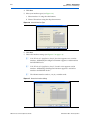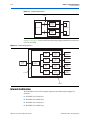
1
POS-PHY Level 2 and 3 Compiler
User Guide
c The IP described in this document is scheduled for product obsolescence and
discontinued support as described in PDN0906. Therefore, Altera® does not
recommend use of this IP in new designs. For more information about Altera’s
current IP offering, refer to Altera’s Intellectual Property website.
101 Innovation Drive
San Jose, CA 95134
www.altera.com
MegaCore Version:
Document Date:
9.1
November 2009
Copyright © 2009 Altera Corporation. All rights reserved. Altera, The Programmable Solutions Company, the stylized Altera logo, specific device designations, and all other
words and logos that are identified as trademarks and/or service marks are, unless noted otherwise, the trademarks and service marks of Altera Corporation in the U.S. and other
countries. All other product or service names are the property of their respective holders. Altera products are protected under numerous U.S. and foreign patents and pending applications, maskwork rights, and copyrights. Altera warrants performance of its semiconductor products to current specifications in accordance with Altera's standard warranty,
but reserves the right to make changes to any products and services at any time without notice. Altera assumes no responsibility or liability arising out of the application or use of
any information, product, or service described herein except as expressly agreed to in writing by Altera Corporation. Altera customers are advised to obtain the latest version of
device specifications before relying on any published information and before placing orders for products or services.
UG-POSPHY2_3-9.1
Contents
Chapter 1. About This Compiler
Release Information . . . . . . . . . . . . . . . . . . . . . . . . . . . . . . . . . . . . . . . . . . . . . . . . . . . . . . . . . . . . . . . . . . . . . 1–1
Device Family Support . . . . . . . . . . . . . . . . . . . . . . . . . . . . . . . . . . . . . . . . . . . . . . . . . . . . . . . . . . . . . . . . . . . 1–1
Features . . . . . . . . . . . . . . . . . . . . . . . . . . . . . . . . . . . . . . . . . . . . . . . . . . . . . . . . . . . . . . . . . . . . . . . . . . . . . . . . 1–2
General Description . . . . . . . . . . . . . . . . . . . . . . . . . . . . . . . . . . . . . . . . . . . . . . . . . . . . . . . . . . . . . . . . . . . . . 1–3
Atlantic Interface . . . . . . . . . . . . . . . . . . . . . . . . . . . . . . . . . . . . . . . . . . . . . . . . . . . . . . . . . . . . . . . . . . . . . 1–4
OpenCore Plus Evaluation . . . . . . . . . . . . . . . . . . . . . . . . . . . . . . . . . . . . . . . . . . . . . . . . . . . . . . . . . . . . . 1–4
Performance and Resource Utilization . . . . . . . . . . . . . . . . . . . . . . . . . . . . . . . . . . . . . . . . . . . . . . . . . . . . . . 1–5
Chapter 2. Getting Started
Design Flow . . . . . . . . . . . . . . . . . . . . . . . . . . . . . . . . . . . . . . . . . . . . . . . . . . . . . . . . . . . . . . . . . . . . . . . . . . . . 2–1
POS-PHY Level 2 & 3 Walkthrough . . . . . . . . . . . . . . . . . . . . . . . . . . . . . . . . . . . . . . . . . . . . . . . . . . . . . . . . 2–2
Create a New Quartus II Project . . . . . . . . . . . . . . . . . . . . . . . . . . . . . . . . . . . . . . . . . . . . . . . . . . . . . . . . . 2–2
Launch IP Toolbench . . . . . . . . . . . . . . . . . . . . . . . . . . . . . . . . . . . . . . . . . . . . . . . . . . . . . . . . . . . . . . . . . . 2–3
Step 1: Parameterize . . . . . . . . . . . . . . . . . . . . . . . . . . . . . . . . . . . . . . . . . . . . . . . . . . . . . . . . . . . . . . . . . . . 2–5
Step 2: Set Up Simulation . . . . . . . . . . . . . . . . . . . . . . . . . . . . . . . . . . . . . . . . . . . . . . . . . . . . . . . . . . . . . . 2–9
Step 3: Generate . . . . . . . . . . . . . . . . . . . . . . . . . . . . . . . . . . . . . . . . . . . . . . . . . . . . . . . . . . . . . . . . . . . . . 2–10
Simulate the Design . . . . . . . . . . . . . . . . . . . . . . . . . . . . . . . . . . . . . . . . . . . . . . . . . . . . . . . . . . . . . . . . . . . . 2–12
IP Functional Simulation Model . . . . . . . . . . . . . . . . . . . . . . . . . . . . . . . . . . . . . . . . . . . . . . . . . . . . . . . . 2–13
Testbench with the ModelSim Simulator . . . . . . . . . . . . . . . . . . . . . . . . . . . . . . . . . . . . . . . . . . . . . . 2–13
Testbench with NativeLink . . . . . . . . . . . . . . . . . . . . . . . . . . . . . . . . . . . . . . . . . . . . . . . . . . . . . . . . . 2–13
Compile the Design . . . . . . . . . . . . . . . . . . . . . . . . . . . . . . . . . . . . . . . . . . . . . . . . . . . . . . . . . . . . . . . . . . . . . 2–15
Program a Device . . . . . . . . . . . . . . . . . . . . . . . . . . . . . . . . . . . . . . . . . . . . . . . . . . . . . . . . . . . . . . . . . . . . . . 2–15
Set Up Licensing . . . . . . . . . . . . . . . . . . . . . . . . . . . . . . . . . . . . . . . . . . . . . . . . . . . . . . . . . . . . . . . . . . . . . . . 2–16
Chapter 3. Functional Description
Example Configurations . . . . . . . . . . . . . . . . . . . . . . . . . . . . . . . . . . . . . . . . . . . . . . . . . . . . . . . . . . . . . . . . . . 3–2
Example Implementations . . . . . . . . . . . . . . . . . . . . . . . . . . . . . . . . . . . . . . . . . . . . . . . . . . . . . . . . . . . . . . . . 3–3
Internal Architecture . . . . . . . . . . . . . . . . . . . . . . . . . . . . . . . . . . . . . . . . . . . . . . . . . . . . . . . . . . . . . . . . . . . . . 3–4
POS-PHY Interface . . . . . . . . . . . . . . . . . . . . . . . . . . . . . . . . . . . . . . . . . . . . . . . . . . . . . . . . . . . . . . . . . 3–5
Packet Data Width Conversion . . . . . . . . . . . . . . . . . . . . . . . . . . . . . . . . . . . . . . . . . . . . . . . . . . . . . . . 3–6
Packet FIFO Buffer . . . . . . . . . . . . . . . . . . . . . . . . . . . . . . . . . . . . . . . . . . . . . . . . . . . . . . . . . . . . . . . . . . 3–6
‘B’ Interface . . . . . . . . . . . . . . . . . . . . . . . . . . . . . . . . . . . . . . . . . . . . . . . . . . . . . . . . . . . . . . . . . . . . . . . . 3–6
OpenCore Plus Time-Out Behavior . . . . . . . . . . . . . . . . . . . . . . . . . . . . . . . . . . . . . . . . . . . . . . . . . . . . . . . . 3–6
© November 2009 Altera Corporation
POS-PHY Level 2 and 3 Compiler User Guide
Preliminary
iv
Parameters . . . . . . . . . . . . . . . . . . . . . . . . . . . . . . . . . . . . . . . . . . . . . . . . . . . . . . . . . . . . . . . . . . . . . . . . . . . . . 3–7
Interface Settings . . . . . . . . . . . . . . . . . . . . . . . . . . . . . . . . . . . . . . . . . . . . . . . . . . . . . . . . . . . . . . . . . . . . . . 3–7
FIFO Buffer & Clock Selector Options . . . . . . . . . . . . . . . . . . . . . . . . . . . . . . . . . . . . . . . . . . . . . . . . . 3–7
Common B Clock . . . . . . . . . . . . . . . . . . . . . . . . . . . . . . . . . . . . . . . . . . . . . . . . . . . . . . . . . . . . . . . . . . . 3–8
Parity Settings . . . . . . . . . . . . . . . . . . . . . . . . . . . . . . . . . . . . . . . . . . . . . . . . . . . . . . . . . . . . . . . . . . . . . . . . 3–8
Pass Through Mode . . . . . . . . . . . . . . . . . . . . . . . . . . . . . . . . . . . . . . . . . . . . . . . . . . . . . . . . . . . . . . . . . 3–8
ParErr On Error Pin . . . . . . . . . . . . . . . . . . . . . . . . . . . . . . . . . . . . . . . . . . . . . . . . . . . . . . . . . . . . . . . . . 3–9
FIFO Buffer Settings . . . . . . . . . . . . . . . . . . . . . . . . . . . . . . . . . . . . . . . . . . . . . . . . . . . . . . . . . . . . . . . . . . . 3–9
Atlantic Interface FIFO Buffer Settings . . . . . . . . . . . . . . . . . . . . . . . . . . . . . . . . . . . . . . . . . . . . . . . . 3–13
FIFO Buffer Size . . . . . . . . . . . . . . . . . . . . . . . . . . . . . . . . . . . . . . . . . . . . . . . . . . . . . . . . . . . . . . . . . . . 3–15
Address & Packet Available Settings . . . . . . . . . . . . . . . . . . . . . . . . . . . . . . . . . . . . . . . . . . . . . . . . . . . 3–15
POS-PHY Level 3 Interfaces . . . . . . . . . . . . . . . . . . . . . . . . . . . . . . . . . . . . . . . . . . . . . . . . . . . . . . . . . 3–15
POS-PHY Level 2 Interfaces . . . . . . . . . . . . . . . . . . . . . . . . . . . . . . . . . . . . . . . . . . . . . . . . . . . . . . . . . 3–15
Base Address . . . . . . . . . . . . . . . . . . . . . . . . . . . . . . . . . . . . . . . . . . . . . . . . . . . . . . . . . . . . . . . . . . . . . 3–16
SX Always . . . . . . . . . . . . . . . . . . . . . . . . . . . . . . . . . . . . . . . . . . . . . . . . . . . . . . . . . . . . . . . . . . . . . . . . 3–16
Interface Signals . . . . . . . . . . . . . . . . . . . . . . . . . . . . . . . . . . . . . . . . . . . . . . . . . . . . . . . . . . . . . . . . . . . . . . . . 3–16
Global Interface . . . . . . . . . . . . . . . . . . . . . . . . . . . . . . . . . . . . . . . . . . . . . . . . . . . . . . . . . . . . . . . . . . . . . . 3–17
POS-PHY Level 3 Interface . . . . . . . . . . . . . . . . . . . . . . . . . . . . . . . . . . . . . . . . . . . . . . . . . . . . . . . . . . . . 3–17
POS-PHY Level 2 Interface . . . . . . . . . . . . . . . . . . . . . . . . . . . . . . . . . . . . . . . . . . . . . . . . . . . . . . . . . . . . 3–22
Atlantic Interface . . . . . . . . . . . . . . . . . . . . . . . . . . . . . . . . . . . . . . . . . . . . . . . . . . . . . . . . . . . . . . . . . . . . 3–26
Timing . . . . . . . . . . . . . . . . . . . . . . . . . . . . . . . . . . . . . . . . . . . . . . . . . . . . . . . . . . . . . . . . . . . . . . . . . . . 3–29
Signal Naming Convention . . . . . . . . . . . . . . . . . . . . . . . . . . . . . . . . . . . . . . . . . . . . . . . . . . . . . . . . . 3–30
Compatibility . . . . . . . . . . . . . . . . . . . . . . . . . . . . . . . . . . . . . . . . . . . . . . . . . . . . . . . . . . . . . . . . . . . . . 3–31
Example Packet Types . . . . . . . . . . . . . . . . . . . . . . . . . . . . . . . . . . . . . . . . . . . . . . . . . . . . . . . . . . . . . 3–31
MegaCore Verification . . . . . . . . . . . . . . . . . . . . . . . . . . . . . . . . . . . . . . . . . . . . . . . . . . . . . . . . . . . . . . . . . . 3–31
Additional Information
Revision History . . . . . . . . . . . . . . . . . . . . . . . . . . . . . . . . . . . . . . . . . . . . . . . . . . . . . . . . . . . . . . . . . . . . . . . . 1–1
How to Contact Altera . . . . . . . . . . . . . . . . . . . . . . . . . . . . . . . . . . . . . . . . . . . . . . . . . . . . . . . . . . . . . . . . . . . 1–1
Typographic Conventions . . . . . . . . . . . . . . . . . . . . . . . . . . . . . . . . . . . . . . . . . . . . . . . . . . . . . . . . . . . . . . . . 1–1
POS-PHY Level 2 and 3 Compiler User Guide
© November 2009 Altera Corporation
Preliminary
1. About This Compiler
Release Information
Table 1–1 provides information about this release of the Altera® POS-PHY Level 2 and
3 Compiler.
Table 1–1. POS-PHY Level 2 and 3 Compiler Release Information
Item
Description
Version
9.1
November 2009
Release Date
Ordering Codes:
■
POS-PHY level 2 PHY
IP-POSPHY/P2
■
POS-PHY level 2 link
IP-POSPHY/L2
■
POS-PHY level 3 PHY
IP-POSPHY/P3
■
POS-PHY level 3 link
IP-POSPHY/L3
Product IDs:
■
POS-PHY level 2 PHY
0058 0071
■
POS-PHY level 2 link
0070 0071
■
POS-PHY level 2 PHY
0051 0071
■
POS-PHY level 2 link
0050 0071
Vendor ID
f
6AF7
For more information about this release, refer to the MegaCore IP Library Release Notes
and Errata.
Altera verifies that the current version of the Quartus® II software compiles the
previous version of each MegaCore® function. The MegaCore IP Library Release Notes
and Errata report any exceptions to this verification. Altera does not verify
compilation with MegaCore function versions older than one release."
Device Family Support
MegaCore functions provide either full or preliminary support for target Altera
device families:
■
Full support means the MegaCore function meets all functional and timing
requirements for the device family and may be used in production designs
■
Preliminary support means the MegaCore function meets all functional
requirements, but may still be undergoing timing analysis for the device family; it
may be used in production designs with caution.
Table 1–2 shows the level of support offered by the POS-PHY Level 2 and 3 Compiler
to each Altera device family.
© November 2009
Altera Corporation
POS-PHY Level 2 and 3 Compiler User Guide
Preliminary
1–2
Chapter 1: About This Compiler
Features
Table 1–2. Device Family Support
Device Family
Support
Arria™ GX
Full
Arria II GX
Preliminary
Cyclone®
Full
Cyclone II
Full
Cyclone III
Full
HardCopy II
Full
HardCopy III
Preliminary
HardCopy IV E
Preliminary
Stratix®
Full
Stratix II
Full
Stratix II GX
Full
Stratix III
Full
Stratix IV
Preliminary
Stratix GX
Full
Other device families
No support
®
Features
■
Conforms to POS-PHY level 2 and level 3 specifications
■
Link-layer or PHY-layer POS-PHY interfaces
■
Creates bridges between different POS-PHY interfaces
■
Support for traffic up to a rate of 3.2 gigabits per second (Gbps) (POS-PHY level 3)
or 832 megabits per second (Mbps) (POS-PHY level 2), such as SONET OC-48
■
Single-PHY (SPHY) or up to 8-channel multi-PHY (MPHY) operation with polled
and direct packet available options
■
Atlantic™ interface that allows a consistent interface between all Altera cell and
packet MegaCore functions
■
Selectable POS-PHY interface bus widths (8/16/32 bit) and Atlantic interface bus
widths (8/16/32/64 bit)—allowing translation between different bus types
■
Parity generation/detection
■
Configurable first-in first-out (FIFO) options: selectable FIFO width, depth, and fill
thresholds.
■
Easy-to-use IP Toolbench interface
■
IP functional simulation models for use in Altera-supported VHDL and Verilog
HDL simulators
■
Support for OpenCore Plus evaluation
POS-PHY Level 2 and 3 Compiler User Guide
© November 2009 Altera Corporation
Preliminary
Chapter 1: About This Compiler
General Description
1–3
General Description
The POS-PHY Level 2 and 3 Compiler generates MegaCore functions for use in linklayer or physical layer (PHY) devices that transfer data to and from packet over
SONET/SDH (POS) devices using the standard POS-PHY bus.
The POS-PHY Level 2 and 3 Compiler comprises separately configurable modules,
which can be easily combined via the IP Toolbench to generate a highly
parameterized module, allowing POS-PHY compliant interfaces (and non-standard
interfaces) to be included in custom designs.
The compiler supports POS-PHY level 3 operating at up to 3.2 Gbps, and level 2
operating at up to 832 Mbps.
The POS-PHY Level 2 and 3 Compiler is compliant with all applicable standards,
including:
■
POS-PHY Level 3 Specification, Issue 4, June 2000
■
POS-PHY Level 2 Specification, Issue 5, December 1998
■
Optical Internet working Forum (OIF), System Packet Interface Level 3 (SPI-3)
■
Altera Corporation, Atlantic Interface Specification
This allows efficient translation between the different formats, including mapping
between different bus speeds and bus widths, as well as customizable FIFO buffer
parameters.
The compiler allows configurations such as PHY-PHY, link-link bridges, or packet
multiplexing MegaCore functions, and SPHY and MPHY applications. Figure 1–1 on
page 1–3 shows the possible interfaces. Figure 1–2 on page 1–4 shows the possible
bridges.
Figure 1–1. Interfaces
MegaCore
Function
PHY
Interface
SPHY
MegaCore
Function
PHY/Link
Interface
© November 2009
Atlantic
Interface
User
Logic
SPHY
MegaCore
Function
MPHY
User
Logic
SPHY
Link
Interface
SPHY
Atlantic
Interface
Atlantic
Interface
User
Logic
Atlantic
Interface
User
Logic
Atlantic
Interface
User
Logic
SPHY
Altera Corporation
POS-PHY Level 2 and 3 Compiler User Guide
Preliminary
1–4
Chapter 1: About This Compiler
General Description
Figure 1–2. Bridges
Level 2/3
Link
Interface
MegaCore
Function
Level 2/3
Link
Interface
SPHY
SPHY
Level 2/3
PHY
Interface
MegaCore
Function
Level 2/3
PHY
Interface
SPHY
SPHY
Level 2/3
Link
Interface
MegaCore
Function
Level 2/3
PHY
Interface
SPHY
SPHY
MegaCore
Function
Level 2/3
PHY/Link
Interface
Level 2/3
PHY/Link
Interface
Level 2/3
PHY/Link
Interface
SPHY
MPHY
Level 2/3
PHY/Link
Interface
Atlantic Interface
The Atlantic interface allows a consistent interface between all Altera cell and packet
MegaCore functions. The Atlantic interface supports a point-to-point connection.
f
For more information on the Atlantic interface, refer to FS 13: Atlantic Interface.
OpenCore Plus Evaluation
With Altera's free OpenCore Plus evaluation feature, you can perform the following
actions:
■
Simulate the behavior of a megafunction (Altera MegaCore function or AMPPSM
megafunction) within your system
■
Verify the functionality of your design, as well as evaluate its size and speed
quickly and easily
■
Generate time-limited device programming files for designs that include
megafunctions
■
Program a device and verify your design in hardware
POS-PHY Level 2 and 3 Compiler User Guide
© November 2009 Altera Corporation
Preliminary
Chapter 1: About This Compiler
Performance and Resource Utilization
1–5
You only need to purchase a license for the megafunction when you are completely
satisfied with its functionality and performance, and want to take your design to
production.
f
For more information on OpenCore Plus hardware evaluation using the POS-PHY
Level 2 and 3 Compiler, see “OpenCore Plus Time-Out Behavior” on page 3–6 and AN
320: OpenCore Plus Evaluation of Megafunctions.
Performance and Resource Utilization
Table 1–3 through 1–7 show typical expected performance for SPHY and 4-port POSPHY MegaCore functions. All results are push-button performance and use a FIFO
buffer size of 512 bytes. These results were obtained using the Quartus® II software
version for the following devices:
■
Cyclone II (see tables for device details)
■
Cyclone III (EP3C5F256C6 for POS-PHY level 3)
■
Stratix III (EP3SL70F484C2 for POS-PHY level 2; EP3SL50F484C2 for POS-PHY
level 3)
■
Stratix IV (EP4SGX70DF29C2X )
Table 1–3. Performance—POS-PHY Level 2 Link Layer—Cyclone II Device
Memory Blocks
LEs
M4K
fMAX (MHz)
SPHY receive
416
2
176
SPHY transmit
407
2
149
MPHY 4-port receive
1,267
8
167
MPHY 4-port transmit
1,272
8
128
MegaCore Function
Device: EP2C5F256C6
Device: EP2C15AF484C6
Table 1–4. Performance—POS-PHY Level 2 Link Layer—Stratix III Device
Memory Blocks
ALUTs
Logic
Registers
M9K
fMAX (MHz)
SPHY receive
177
348
2
344
SPHY transmit
210
326
2
310
MPHY 4-port receive
558
1,051
8
320
MPHY 4-port transmit
624
1,024
8
221
MegaCore Function
Table 1–5. Performance—POS-PHY Level 2 PHY Layer—Cyclone II Device (Part 1 of 2)
Memory Blocks
MegaCore Function
LEs
M4K
fMAX (MHz)
354
2
174
Device: EP2C5F256C6
SPHY receive
© November 2009
Altera Corporation
POS-PHY Level 2 and 3 Compiler User Guide
Preliminary
1–6
Chapter 1: About This Compiler
Performance and Resource Utilization
Table 1–5. Performance—POS-PHY Level 2 PHY Layer—Cyclone II Device (Part 2 of 2)
Memory Blocks
LEs
M4K
fMAX (MHz)
285
2
159
MPHY 4-port receive
1,175
8
161
MPHY 4-port transmit
1,126
8
139
MegaCore Function
SPHY transmit
Device: EP2C15AF484C6
Table 1–6. Performance—POS-PHY Level 2 PHY Layer—Stratix III Device
Memory Blocks
ALUTs
Logic
Registers
M9K
fMAX (MHz)
SPHY receive
122
309
2
340
SPHY transmit
123
234
2
346
MegaCore Function
MPHY 4-port receive
487
995
8
318
MPHY 4-port transmit
529
918
8
293
Table 1–7. Performance—POS-PHY Level 3 Link Layer—Cyclone III Device
Memory Blocks
LEs
M9K
fMAX (MHz)
SPHY receive
379
2
165
SPHY transmit
377
2
139
MPHY 4-port receive
1,202
8
171
MPHY 4-port transmit
1,242
8
164
MegaCore Function
Table 1–8. Performance—POS-PHY Level 3 Link Layer—Stratix III Device
Memory Blocks
ALUTs
Logic
Registers
M9K
fMAX (MHz)
SPHY receive
149
330
2
234
SPHY transmit
164
313
2
205
MPHY 4-port receive
522
1,019
8
217
MPHY 4-port transmit
613
1,009
8
178
MegaCore Function
Table 1–9. Performance—POS-PHY Level 3 Link Layer—Stratix IV Device
Memory Blocks
ALUTs
Logic
Registers
M9K
fMAX (MHz)
SPHY receive
149
330
2
231
SPHY transmit
164
313
2
180
MPHY 4-port receive
522
1,019
8
254
MPHY 4-port transmit
613
1,009
8
174
MegaCore Function
POS-PHY Level 2 and 3 Compiler User Guide
© November 2009 Altera Corporation
Preliminary
Chapter 1: About This Compiler
Performance and Resource Utilization
1–7
Table 1–10. Performance—POS-PHY Level 3 PHY Layer—Cyclone III Device
Memory Blocks
LEs
M4K
fMAX (MHz)
SPHY receive
350
2
174
SPHY transmit
365
2
173
MPHY 4-port receive
1,175
8
169
MPHY 4-port transmit
1,218
8
143
MegaCore Function
Table 1–11. Performance—POS-PHY Level 3 PHY Layer—Stratix III Device
Memory Blocks
ALUTs
Logic
Registers
M9K
fMAX (MHz)
SPHY receive
121
307
2
270
SPHY transmit
160
294
2
287
MegaCore Function
MPHY 4-port receive
489
999
8
245
MPHY 4-port transmit
587
984
8
231
Table 1–12. Performance—POS-PHY Level 3 PHY Layer—Stratix IV Device
Memory Blocks
ALUTs
Logic
Registers
M9K
fMAX (MHz)
SPHY receive
121
307
2
243
SPHY transmit
160
294
2
286
MPHY 4-port receive
489
999
8
222
MPHY 4-port transmit
587
984
8
260
MegaCore Function
© November 2009
Altera Corporation
POS-PHY Level 2 and 3 Compiler User Guide
Preliminary
1–8
Chapter 1: About This Compiler
Performance and Resource Utilization
POS-PHY Level 2 and 3 Compiler User Guide
© November 2009 Altera Corporation
Preliminary
2. Getting Started
Design Flow
To evaluate the POS-PHY Level 2 and 3 Compiler using the OpenCore Plus feature
include these steps in your design flow:
1. Obtain and install the POS-PHY Level 2 and 3 Compiler.
The POS-PHY Level 2 and 3 MegaCore function is part of the MegaCore IP
Library, which is distributed with the Quartus® II software and downloadable
from the Altera® website, www.altera.com.
f
For system requirements and installation instructions, refer to Quartus II
Installation & Licensing for Windows and Linux Workstations.
Figure 2–1 on page 2–1 shows the directory structure after you install the POSPHY Level 2 and 3 Compiler, where <path> is the installation directory. The default
installation directory on Windows is c:\altera\90; on Linux it is /opt/altera90.
Figure 2–1. Directory Structure
<path>
Installation directory.
ip
Contains the Altera MegaCore IP Library and third-party IP cores.
altera
Contains the Altera MegaCore IP Library.
common
Contains shared components.
posphy_l2_l3
Contains the POS-PHY Level 2 and 3 Compiler files and documentation.
doc
Contains the documentation for the MegaCore function.
lib
Contains encrypted lower-level design files.
sim_lib
Contains the MegaCore function simulation models.
modelsim
Contains the ModelSim simulation models.
testbench
Contains the testbench.
2. Create a custom variation of a POS-PHY Level 2 or 3 MegaCore function using IP
Toolbench.
1
© November 2009
IP Toolbench is a toolbar from which you can quickly and easily view
documentation, specify parameters, and generate all of the files necessary
for integrating the parameterized MegaCore function into your design.
Altera Corporation
POS-PHY Level 2 and 3 Compiler User Guide
Preliminary
2–2
Chapter 2: Getting Started
POS-PHY Level 2 & 3 Walkthrough
3. Implement the rest of your design using the design entry method of your choice.
4. Use the IP Toolbench-generated IP functional simulation model to verify the
operation of your design.
f
For more information on IP functional simulation models, refer to the Simulating
Altera IP in Third-Party Simulation Tools chapter in volume 3 of the Quartus II Handbook.
5. Use the Quartus II software to compile your design.
1
You can also generate an OpenCore Plus time-limited programming file,
which you can use to verify the operation of your design in hardware.
6. Purchase a license for the POS-PHY Level 2 and 3 Compiler.
After you have purchased a license for the POS-PHY Level 2 and 3 compiler, the
design flow requires these additional steps:
1. Set up licensing.
2. Generate a programming file for the Altera® device(s) on your board.
3. Program the Altera device(s) with the completed design.
4. Perform design verification.
POS-PHY Level 2 & 3 Walkthrough
This walkthrough explains how to create a POS-PHY Level 2 or 3 MegaCore function
using the Altera POS-PHY Level 2 and 3 Compiler IP Toolbench and the Quartus II
software. When you finish generating a POS-PHY Level 2 or 3 MegaCore function,
you can incorporate it into your overall project.
1
IP Toolbench only allows you to select legal combinations of parameters, and warns
you of any invalid configurations.
This walkthrough involves the following steps:
■
Create a New Quartus II Project
■
Launch IP Toolbench
■
Step 1: Parameterize
■
Step 2: Set Up Simulation
■
Step 3: Generate
Create a New Quartus II Project
You need to create a new Quartus II project with the New Project Wizard, which
specifies the working directory for the project, assigns the project name, and
designates the name of the top-level design entity.
To create a new project follow these steps:
POS-PHY Level 2 and 3 Compiler User Guide
© November 2009 Altera Corporation
Preliminary
Chapter 2: Getting Started
POS-PHY Level 2 & 3 Walkthrough
2–3
1. Choose Programs > Altera > Quartus II <version> (Windows Start menu) to run
the Quartus II software. Alternatively, you can also use the Quartus II Web
Edition software.
2. Choose New Project Wizard (File menu).
3. Click Next in the New Project Wizard Introduction page (the introduction does
not display if you turned it off previously).
4. In the New Project Wizard: Directory, Name, Top-Level Entity page, enter the
following information:
a. Specify the working directory for your project. For example, this walkthrough
uses the c:\altera\projects\pl2pl3_project directory.
1
The Quartus II software automatically specifies a top-level design entity
that has the same name as the project. This walkthrough assumes that the
names are the same.
b. Specify the name of the project. This walkthrough uses example for the project
name.
5. Click Next to close this page and display the New Project Wizard: Add Files page.
1
When you specify a directory that does not already exist, a message asks if
the specified directory should be created. Click Yes to create the directory.
6. Click Next to close this page and display the New Project Wizard: Family &
Device Settings page.
7. On the New Project Wizard: Family & Device Settings page, choose the target
device family in the Family list.
8. The remaining pages in the New Project Wizard are optional. Click Finish to
complete the Quartus II project.
You have finished creating your new Quartus II project.
Launch IP Toolbench
To launch IP Toolbench in the Quartus II software, follow these steps:
1. Start the MegaWizard® Plug-In Manager by choosing MegaWizard Plug-In
Manager (Tools menu). The MegaWizard Plug-In Manager dialog box displays.
1
© November 2009
Refer to the Quartus II Help for more information on how to use the
MegaWizard Plug-In Manager.
Altera Corporation
POS-PHY Level 2 and 3 Compiler User Guide
Preliminary
2–4
Chapter 2: Getting Started
POS-PHY Level 2 & 3 Walkthrough
Figure 2–2. MegaWizard Plug-In Manager
2. Specify that you want to create a new custom megafunction variation and click
Next.
3. Expand the Communications > POS-PHY directory then click POS-PHY Level 2
& 3 Compiler.
4. Select the output file type for your design; the wizard supports VHDL, and
Verilog HDL.
5. The MegaWizard Plug-In Manager shows the project path that you specified in the
New Project Wizard. Append a variation name for the MegaCore function output
files <project path>\<variation name>. Figure 2–3 shows the wizard after you have
made these settings.
Figure 2–3. Select the Megafunction
6. Click Next to launch IP Toolbench.
POS-PHY Level 2 and 3 Compiler User Guide
© November 2009 Altera Corporation
Preliminary
Chapter 2: Getting Started
POS-PHY Level 2 & 3 Walkthrough
2–5
Step 1: Parameterize
To parameterize your MegaCore function, follow these steps:
1. Click Parameterize in the IP Toolbench (see Figure 2–4 on page 2–5).
Figure 2–4. IP Toolbench—Parameterize
2. Select your architecture options where the POS-PHY ‘A’ interface is a data source
or sink (see Figure 2–5).
1
Source indicates that interface ‘A’ is an output from the MegaCore function.
Sink indicates that interface ‘A’ is an input to the MegaCore function.
Figure 2–5. Select the ‘A’ Interface Direction
3. In a MPHY architecture there is a ‘B’ interface for each supported channel
(maximum eight). Select the number of supported channels that you require.
1
© November 2009
To create a design that supports source and sink data directions, you must
run IP Toolbench twice, to create the source and sink designs separately.
Altera Corporation
POS-PHY Level 2 and 3 Compiler User Guide
Preliminary
2–6
Chapter 2: Getting Started
POS-PHY Level 2 & 3 Walkthrough
4. Click Next.
5. Select your interface types (see Figure 2–6).
a. Select interface ‘A’ using the radio buttons.
b. Choose ‘B’ interfaces using the drop-down menus.
Figure 2–6. Select the Interface Types
6. Click Next.
7. Choose the interface settings (see Figure 2–7 on page 2–6).
1
POS-PHY Level 3 Specification, Issue 4, June 2000 supports an 8- or 32-bit
interface. Additionally this MegaCore function supports a 16-bit interface
for POS-PHY level 3.
1
POS-PHY Level 2 Specification, Issue 5, December 1998 supports a 16 bit
interface. Additionally, this MegaCore function supports 8- and 32-bit
interfaces for POS-PHY level 2.
1
The Atlantic interface can be 8-, 16-, 32-, or 64-bits wide.
Figure 2–7. Choose the Interface Settings
POS-PHY Level 2 and 3 Compiler User Guide
© November 2009 Altera Corporation
Preliminary
Chapter 2: Getting Started
POS-PHY Level 2 & 3 Walkthrough
2–7
8. Click Next.
9. Select the parity settings of the interfaces (see Figure 2–8).
1
If parity is used the polarity setting must be the same for all interfaces.
Figure 2–8. Select the Parity Settings
f
For more information on the parity settings, see “Parity Settings” on page 3–8.
10. Click Next.
11. Choose the first-in first-out (FIFO) buffer settings (see Figure 2–9).
Figure 2–9. Choose the FIFO Buffer Settings
If you select the Fixed Burst option, you must also set the burst size by entering a
value in the Burst field. Data is then sent in bursts of the specified burst size only,
or in bursts containing an end of packet.
© November 2009
Altera Corporation
POS-PHY Level 2 and 3 Compiler User Guide
Preliminary
2–8
Chapter 2: Getting Started
POS-PHY Level 2 & 3 Walkthrough
1
The wizard indicates the minimum Burst value supported.
You must also adjust the FIFO thresholds so that the data sent to the FIFO for a
burst is greater than the burst (an end of packet of packet flushes the FIFO). The
minimum and maximum values are set as follows:
■
The minimum value must be set at the size of the remote burst. If you set any
value below this, it is automatically adjusted to the size of the remote burst.
■
The maximum value is derived from the empty threshold. It must take into
account the latency in the pipeline and the time that the core takes to decide to
stop sending data. Therefore, the maximum burst size is calculated as follows:
(‘A’ interface empty threshold in bytes) – (5 × fifo_byte_width)
Where fifo_byte_width is the width in bytes of the FIFO (4 for a 32-bit data
width).
f
For more information on the FIFO buffer settings, see “FIFO Buffer Settings” on
page 3–9.
12. Click Next.
13. Choose the address and packet available settings (see Figure 2–10).
Figure 2–10. Choose the Address and Packet Available Settings
f
For more information on the address and packet available settings, see “Address &
Packet Available Settings” on page 3–15.
14. Click Next.
15. IP Toolbench shows the product order codes (see Figure 2–11). Click Finish.
POS-PHY Level 2 and 3 Compiler User Guide
© November 2009 Altera Corporation
Preliminary
Chapter 2: Getting Started
POS-PHY Level 2 & 3 Walkthrough
2–9
Figure 2–11. Product Order Code
Step 2: Set Up Simulation
An IP functional simulation model is a cycle-accurate VHDL or Verilog HDL model
produced by the Quartus II software. It allows for fast functional simulation of IP
using industry-standard VHDL and Verilog HDL simulators.
c
You may only use these simulation model output files for simulation purposes and
expressly not for synthesis or any other purposes. Using these models for synthesis
will create a nonfunctional design.
To generate an IP functional simulation model for your MegaCore function, follow
these steps:
1. Click Set Up Simulation in IP Toolbench (see Figure 2–12 on page 2–9).
Figure 2–12. IP Toolbench—Set Up Simulation
2. Turn on Generate Simulation Model (see Figure 2–13).
© November 2009
Altera Corporation
POS-PHY Level 2 and 3 Compiler User Guide
Preliminary
2–10
Chapter 2: Getting Started
POS-PHY Level 2 & 3 Walkthrough
Figure 2–13. Generate Simulation Model
3. Choose the language in the Language list.
4. Some third-party synthesis tools can use a netlist that contains only the structure
of the MegaCore function, but not detailed logic, to optimize performance of the
design that contains the MegaCore function. If your synthesis tool supports this
feature, turn on Generate netlist.
5. Click OK.
Step 3: Generate
To generate your MegaCore function, follow these steps:
1. Click Step 3: Generate in IP Toolbench (see Figure 2–14).
POS-PHY Level 2 and 3 Compiler User Guide
© November 2009 Altera Corporation
Preliminary
Chapter 2: Getting Started
POS-PHY Level 2 & 3 Walkthrough
2–11
Figure 2–14. IP Toolbench—Generate
Figure 2–15 on page 2–11 shows the generation report.
Figure 2–15. Generation Report
Table 2–1 describes the generated files and other files that may be in your project
directory. The names and types of files specified in the IP Toolbench report vary
based on whether you created your design with VHDL or Verilog HDL.
© November 2009
Altera Corporation
POS-PHY Level 2 and 3 Compiler User Guide
Preliminary
2–12
Chapter 2: Getting Started
Simulate the Design
Table 2–1. Generated Files
Extension
Description
<variation name>syn.v or
<variation name>syn.vhd
A timing and resource netlist for use in some third-party synthesis tools.
<variation name>.bsf
Quartus II symbol file for the MegaCore function variation. You can use this file in the
Quartus II block diagram editor.
<variation name>.cmp
A VHDL component declaration file for the MegaCore function variation. Add the contents of
this file to any VHDL architecture that instantiates the MegaCore function.
<variation name>.ppf
This XML file describes the MegaCore function pin attributes to the Quartus II Pin Planner.
MegaCore function pin attributes include pin direction, location, I/O standard assignments, and
drive strength. If you launch IP Toolbench outside of the Pin Planner application, you must
explicitly load this file to use Pin Planner.
<variation name>.ppx
This XML file is a Pin Planner support file that Pin Planner automatically uses. This file must
remain in the same directory as the <variation name>.ppf file.
<variation name>.vhd or
<variation name>.v
A MegaCore function variation file, which defines a VHDL or Verilog HDL top-level description
of the custom MegaCore function. Instantiate the entity defined by this file inside your design.
Include this file when compiling your design in the Quartus II software.
<variation name>.vo or
<variation name>.vho
VHDL or Verilog HDL IP functional simulation model.
2. After you review the generation report, click Exit to close IP Toolbench and click
Yes on the Quartus II IP Files message.
1
The Quartus II IP File (.qip) is a file generated by the MegaWizard interface or SOPC
Builder that contains information about a generated IP core. You are prompted to add
this .qip file to the current Quartus II project at the time of file generation. In most
cases, the .qip file contains all of the necessary assignments and information required
to process the core or system in the Quartus II compiler. Generally, a single .qip file is
generated for each MegaCore function and for each SOPC Builder system. However,
some more complex SOPC Builder components generate a separate .qip file, so the
system .qip file references the component .qip file.
You can now integrate your custom MegaCore function variation into your design,
simulate, and compile.
Simulate the Design
You can simulate your design using the IP Toolbench-generated VHDL and Verilog
HDL IP functional simulation models.
f
For more information on IP functional simulation models, refer to “IP Functional
Simulation Model” on page 2–13 and the Simulating Altera IP in Third-Party Simulation
Tools chapter in volume 3 of the Quartus II Handbook.
Altera also provides fixed example VHDL and Verilog HDL testbenches that you can
use to simulate example sink or source POS-PHY systems. You can use a testbench as
a basis for your own design. The testbenches can be used with the IP functional
simulation models. The testbenches and associated files are located in the
sim_lib\testbench directory.
POS-PHY Level 2 and 3 Compiler User Guide
© November 2009 Altera Corporation
Preliminary
Chapter 2: Getting Started
Simulate the Design
2–13
IP Functional Simulation Model
This section tells you how to use the demonstration testbench with the ModelSim
simulator or with other simulators using NativeLink.
f
For more information on NativeLink, refer to the Simulating Altera IP in Third-Party
Simulation Tools chapter in volume 3 of the Quartus II Handbook.
Testbench with the ModelSim Simulator
To use an example testbench with IP functional simulation models in the ModelSim
simulator, follow these steps:
1
The testbench includes pregenerated Verilog HDL IP functional simulation models.
1. Start the ModelSim simulator.
2. Change the directory to the sim_lib\modelsim directory.
3. For VHDL type the following command:
do compile_pl3_link_source_fixed_example_vlog_ipfs.tclr
or for Verilog HDL type the following command:
do compile_pl3_link_source_fixed_example_vhdl_ipfs.tclr
1
For the sink example, replace source with sink.
Testbench with NativeLink
You can run receive and transmit tests with third-party IP functional simulators using
NativeLink, for VHDL or Verilog HDL. The following procedure describes a receive
test for the Verilog HDL model.
To use the testbench with NativeLink, follow these steps:
1. Using the New Project Wizard in the Quartus II software, create a new project in
the \posphy_l2_l3\sim_lib\testbench\verilog directory with the project name
and top-level entity name of auk_pac_mrx_pl3_link.
1
For the VHDL model, replace the verilog directory with the vhdl directory.
1
For the transmit test, replace mrx with mtx.
2. Add the POS-PHY level 2 and 3 library:
a. On the Assignments menu click Settings.
b. Under Category click Libraries
c. In Project library name click ...
d. Browse to \pos_phy_l2l3\lib and click Open.
e. Click Add.
f. Click OK.
© November 2009
Altera Corporation
POS-PHY Level 2 and 3 Compiler User Guide
Preliminary
2–14
Chapter 2: Getting Started
Simulate the Design
3. Add the following files to the project from the \posphy_l2_l3\lib directory:
■
auk_pac_gen_if.vhd
■
auk_pac_functions.vhd
■
auk_pac_components.vhd
The files must be in the order shown, from top to bottom, which is the order of
compilation. Use the Up and Down buttons in the New Project Wizard: Add Files
window to order the files.
4. Check that the absolute path to your third-party simulation tool is set. Set the path
from EDA Tool Options in the Options dialog box (Tools menu).
5. On the Processing menu, point to Start and click Start Analysis & Elaboration.
1
If the analysis and elaboration is not successful, fix the error before moving
to the next step.
6. On the Assignments menu, click Settings. The Settings window appears. Expand
EDA Tool Settings and select Simulation.
7. In Tool name, select a simulator tool from the list.
In EDA Netlist Writer options, select Verilog from the list for Format for output
netlist (Select VHDL if you are preparing a VHDL simulation).
In NativeLink settings, select the Compile test bench option and then click Test
Benches . The Test Benches window appears.
8. In the Test Benches window, click New. The New Test Bench Settings window
appears.
9. In the New Test Bench Settings window, enter the information described in
Table 2–2 (see also Figure 2–16 on page 2–15). To enter the files described in the
table, browse to the files in your project.
Table 2–2. NativeLink Test Bench Settings
Parameter
Setting/File Name
Test bench name
<any name>
Top-level module in test bench
auk_pac_mrx_ref (1)
Design instance name in test bench
mrx (1)
Run for
100 ns
Test bench files
auk_pac_mrx_ref_tb.v (2)
Notes to table:
(1) Use mtx for Tx simulations.
(2) If you are preparing a VHDL simulation, use auk_pac_mrx_ref_tb.vhd in the vhdl directory.
Figure 2–16 shows the testbench settings for a receive simulation.
POS-PHY Level 2 and 3 Compiler User Guide
© November 2009 Altera Corporation
Preliminary
Chapter 2: Getting Started
Compile the Design
2–15
Figure 2–16. Example of New Test Bench Settings for NativeLink
10. When you have entered the required information for your new testbench, click
OK in the New Test Bench Settings window.
11. Click OK in the Test Benches window and then click OK in the Settings window.
12. On the Tools menu, point to Run EDA Simulation Tool and click EDA RTL
Simulation. The simulation now begins with your chosen simulation tool.
Compile the Design
You can use the Quartus II software to compile your design. Refer to Quartus II Help
for instructions on compiling your design.
Program a Device
After you have compiled your design, program your targeted Altera device, and
verify your design in hardware.
With Altera's free OpenCore Plus evaluation feature, you can evaluate the POS-PHY
Level 2 and 3 Compiler before you purchase a license. OpenCore Plus evaluation
allows you to generate an IP functional simulation model, and produce a time-limited
programming file.
f
For more information on IP functional simulation models, refer to the Simulating
Altera IP in Third-Party Simulation Tools chapter in volume 3 of the Quartus II Handbook.
You can simulate the POS-PHY Level 2 and 3 Compiler in your design, and perform a
time-limited evaluation of your design in hardware.
© November 2009
Altera Corporation
POS-PHY Level 2 and 3 Compiler User Guide
Preliminary
2–16
Chapter 2: Getting Started
Set Up Licensing
f
For more information on OpenCore Plus hardware evaluation using the POS-PHY
Level 2 and 3 Compiler, see “OpenCore Plus Evaluation” on page 1–4, “OpenCore
Plus Time-Out Behavior” on page 3–6, and AN 320: OpenCore Plus Evaluation of
Megafunctions.
Set Up Licensing
You need to purchase a license for the MegaCore function only when you are
completely satisfied with its functionality and performance and want to take your
design to production.
After you purchase a license for the POS-PHY Level 2 and 3 MegaCore function, you
can request a license file from the Altera website at www.altera.com/licensing and
install it on your computer. When you request a license file, Altera emails you a
license.dat file. If you do not have Internet access, contact your local Altera
representative.
POS-PHY Level 2 and 3 Compiler User Guide
© November 2009 Altera Corporation
Preliminary
3. Functional Description
The POS-PHY Level 2 and 3 Compiler has two interfaces—an ‘A’ interface and one or
many ‘B’ interfaces. Table 3–1 shows the possible interfaces.
Table 3–1. Possible Interfaces
‘A’ Interface
‘B’ Interface
PHY level 3 (SPHY or MPHY)
PHY level 3 (SPHY only)
PHY level 2 (SPHY or MPHY)
PHY level 2 (SPHY only)
Link level 3 (SPHY or MPHY)
Link level 3 (SPHY only)
Link level 2 (SPHY or MPHY)
Link level 2 (SPHY only)
Atlantic master (SPHY only)
Atlantic slave (SPHY only)
Figure 3–1 and 3–2 show example interfaces.
1
MegaCore® function data flow direction is from source to sink, that is, data flows from
a physical layer (PHY) receive source to a link receive sink. A MegaCore function
must have a minimum of one source and one sink interface.
Figure 3–1. Example MegaCore Function Interfaces
MegaCore Function
'A' Sink
Interface
© November 2009
Altera Corporation
FIFO
'B1' Source
Interface
FIFO
'B2' Source
Interface
FIFO
'B3' Source
Interface
FIFO
'Bn'' Source
Interface
POS-PHY Level 2 and 3 Compiler User Guide
Preliminary
3–2
Chapter 3: Functional Description
Example Configurations
Figure 3–2. Example Interface
MegaCore Function
'A' Source
Interface
FIFO
'B1' Sink
Interface
FIFO
'B2' Sink
Interface
FIFO
'B3' Sink
Interface
FIFO
'Bn'' Sink
Interface
POS-PHY level 3 is a point-to-point system—transmit joins to transmit; channel 0
joins to channel 0, and so on (see Figure 3–3). POS-PHY level 2 is a unidirectional bus
system.
Figure 3–3. Connecting POS-PHY Level 3 MegaCore Functions
PHY Transmit
Function
Sink
Interface
Source
Interface
Link Transmit
Function
PHY Receive
Function
Source
Interface
Sink
Interface
Link Receive
Function
Example Configurations
Figure 3–4 on page 3–2 shows a packet-processing function, which receives packets at
one end from a POS-PHY PHY interface, processes them, and passes them on to a
POS-PHY link interface.
Figure 3–4. Example Configuration—Use of the Atlantic Interface
Atlantic
Interfaces
Atlantic
Interfaces
MegaCore Function 1
MegaCore Function 2
FIFO
100 MHz
32 bit
Level 3
Link
Interface
FIFO
FIFO
Packet
Processing
Function
FIFO
FIFO
Level 3
PHY
Interface
100 MHz
32 bit
FIFO
POS-PHY Level 2 and 3 Compiler User Guide
© November 2009 Altera Corporation
Preliminary
Chapter 3: Functional Description
Example Implementations
3–3
Figure 3–5 shows a bridging function with multiple lower-rate ports, which can be 8bit POS-PHY level 3 or 16-bit POS-PHY level 2.
Figure 3–5. Example Configuration 2—POS-PHY Bridging Functions
MegaCore Function 1
100 MHz
32 bit
Level 3
Link
Interface
FIFO
Level 2
PHY
Interface
FIFO
Level 2
PHY
Interface
FIFO
Level 3
PHY
Interface
50 MHz
16 bit
50 MHz
16 bit
100 MHz
8 bit
Figure 3–6 on page 3–3 shows an MPHY to MPHY POS-PHY bridge, which includes
an MPHY POS-PHY level 2 interface and one first-in first-out (FIFO) buffer per
supported address (MPHY).
Figure 3–6. Example Configuration 3—MPHY to MPHY Bridge
Atlantic
Interfaces
MegaCore Function 1
MegaCore Function 2
FIFO
100 MHz
8 bit
Level 3
PHY
Interface
FIFO
Level 2
Link
Interface
50 MHz
16 bit
FIFO
Example Implementations
Figure 3–7 shows the FPGA interfacing to an OC-48 framer.
© November 2009
Altera Corporation
POS-PHY Level 2 and 3 Compiler User Guide
Preliminary
3–4
Chapter 3: Functional Description
Internal Architecture
Figure 3–7. Example Implementation
Atlantic
Interfaces
FPGA
MegaCore Function 1
Level 3 Link
Interface
(Source)
PHY
OC48 Framer
User Logic
MegaCore Function 1
Level 3 Link
Interface
(Sink)
PHY
Figure 3–8 on page 3–4 shows the FPGA interfacing multiple POS-PHY level 2 devices
to an OC-48 switch.
Figure 3–8. Example Implementation 2
FPGA
MegaCore Function
FIFO
Level 2
Link
Interface
Level 2
PHY Device
FIFO
Level 2
Link
Interface
Level 2
PHY Device
FIFO
Level 2
Link
Interface
Level 2
PHY Device
FIFO
Level 2
Link
Interface
Level 2
PHY Device
Level 3
PHY
Interface
OC48
Switch
(Link)
'A' Interface
'B' Interface
Internal Architecture
The POS-PHY Level 2 and 3 Compiler comprises the following four MegaCore
functions:
■
POS-PHY level 2 link-layer
■
POS-PHY level 2 PHY-layer
■
POS-PHY level 3 link-layer
■
POS-PHY level 3 PHY-layer
POS-PHY Level 2 and 3 Compiler User Guide
© November 2009 Altera Corporation
Preliminary
Chapter 3: Functional Description
Internal Architecture
3–5
Each MegaCore function includes a separate receiver and transmitter, which can be
instantiated in a single device or separate devices.
There are many similarities in the internal architecture of these blocks. The main
difference is in the non-symmetrical handshaking on the physical interface between
receive and transmit directions.
Figure 3–9 on page 3–5 shows the sink MegaCore function block diagram. Figure 3–10
on page 3–5 shows the source MegaCore function block diagram.
Figure 3–9. Sink MegaCore Function Block Diagram
Data
Port N
Port 2
Control
Port 1
Data
Port 0
Link-layer or
PHY-Layer
Sink
Interface
Packet Data
Width
Conversion
(wider)
Packet
FIFO
2
1
Link-layer or
PHY-Layer
Source
Interface
Packet Data
Width
Conversion
(narrower)
Control
3
4
'B' Interface Options
Figure 3–10. Source MegaCore Function Block Diagram
Data
Port N
Port 2
Control
Port 1
Multiplexer
Data
Port 0
Link-Layer or
PHY-Layer
Source
Interface
Packet Data
Width
Conversion
(narrower)
Packet Data
Width
Conversion
(wider)
Packet
FIFO
1
2
Link-layer or
PHY-Layer
Sink
Interface
3
Control
4
'B' Interface Options
POS-PHY Interface
Each POS-PHY supports single and multi-PHY implementations. The POS-PHY
interface interfaces to an internal multiplexer, which allows access to multiple/single
internal packet FIFO buffers. Status information from the FIFO buffers is used to
control the POS-PHY interface. The source interface provides polled or direct packet
available modes.
© November 2009
Altera Corporation
POS-PHY Level 2 and 3 Compiler User Guide
Preliminary
3–6
Chapter 3: Functional Description
OpenCore Plus Time-Out Behavior
Packet Data Width Conversion
Packet data width conversion provides conversion from a narrower to a wider data
stream, and from a wider to a narrower data stream, if required (such as, 8-bit to 32or 16-bit, or 32-bit to 8- or 16-bit, and so on).
Packet FIFO Buffer
The packet FIFO buffer has configurable width, depth, and fill level options. The FIFO
buffer stores packet data in line with its associated packet flags (start of packet (SOP),
end of packet (EOP), modulo (mod), and so on.
‘B’ Interface
The ‘B’ interface can be positioned at four different places, as follows:
1. After the first data width conversion—you provide a FIFO-like interface. The data
width must be greater than or equal to the required POS-PHY bus width. Atlantic™
interfaces here can only be masters.
2. After the packet FIFO buffer—you must interface to the internal packet FIFO
buffer at the data width of the FIFO buffer, which is greater than or equal to that of
the required POS-PHY bus. Atlantic interfaces here can be master or a slave
interfaces.
3. After the second data width conversion—this position provides an interface where
the data width can be narrower than that supported by the FIFO buffer. For
example, a 32-bit POS-PHY to or from an 8-bit POS-PHY. Atlantic interfaces here
can be a master or a slave interfaces.
4. After a POS-PHY interface—where you can create a POS-PHY bridge. From a
single compiler you can build a MPHY to multiple SPHY bridge, or an SPHY to
SPHY bridge. You can create more complex solutions by instantiating more than
one MegaCore function.
OpenCore Plus Time-Out Behavior
OpenCore Plus hardware evaluation supports the following two operation modes:
■
Untethered—the design runs for a limited time.
■
Tethered—requires a connection between your board and the host computer. If
tethered mode is supported by all megafunctions in a design, the device can
operate for a longer time or indefinitely.
All megafunctions in a device time out simultaneously when the most restrictive
evaluation time is reached. If there is more than one megafunction in a design, a
specific megafunction’s time-out behavior may be masked by the time-out behavior of
the other megafunctions.
1
For MegaCore functions, the untethered timeout is 1 hour; the tethered timeout value
is indefinite.
Your design stops working after the hardware evaluation time expires and the
following events occur:
POS-PHY Level 2 and 3 Compiler User Guide
© November 2009 Altera Corporation
Preliminary
Chapter 3: Functional Description
Parameters
■
■
f
3–7
For the POS-PHY receive interface:
■
The sop_ina input goes low
■
The addr_outa output goes low
■
The dpav_outa output goes low
■
The ppav_outa output goes low
■
The spav_outa output goes low
■
The rd_outa output goes low
For the POS-PHY transmit interface:
■
The wr_outA output goes low
■
The val_outA output goes low
■
'The sx_outA output goes low
■
The sop_outA output goes low
■
'The eop_outA output goes low
■
The err_outA output goes high
■
The data_outA output goes low
For more information on OpenCore Plus hardware evaluation, see “OpenCore Plus
Evaluation” on page 1–4 and AN 320: OpenCore Plus Evaluation of Megafunctions.
Parameters
The function’s parameters, which can only be set in IP Toolbench (see “Step 1:
Parameterize” on page 2–5), include the following settings:
■
Interface Settings
■
Parity Settings
■
FIFO Buffer Settings
■
Address & Packet Available Settings
Interface Settings
FIFO Buffer & Clock Selector Options
The following interface ‘B’ FIFO buffer and clock selector options are available:
© November 2009
■
A Clock (No FIFO buffer)—only available if the ‘B’ interface is an Atlantic master,
and the ‘B’ interface bus width ≥ the ‘A’ interface bus width. The relevant ‘B’
interface does not use an internal FIFO buffer, and is clocked by the ‘A’ interface
clock pin. This is recommended only if you connect ‘B’ interfaces directly to
another MegaCore function with an Atlantic slave interface
■
A Clock—the corresponding ‘B’ interface uses an internal single clock FIFO buffer,
and is clocked by the A interface clock pin
Altera Corporation
POS-PHY Level 2 and 3 Compiler User Guide
Preliminary
3–8
Chapter 3: Functional Description
Parameters
■
B Clock—the corresponding ‘B’ interface uses an internal dual clock FIFO buffer,
and is clocked by the corresponding ‘B’ interface clock pin
The FIFO buffer width is the greater of the A bus width and the associated B bus
width.
Common B Clock
With MPHY configurations there is more than one ‘B’ interface in the MegaCore
function. Select this option to use a common clock and reset pins for all the ‘B’
interfaces that use the B clock option.
If you select this option, the ‘B’ interface clock and reset pins are labeled b_clk and
b_reset_n.
Parity Settings
This section describes pass through mode and the parerr on error pin.
Pass Through Mode
In pass through mode any detected data parity errors on a sink interface are
regenerated on the source interface, even when there is a bus width change.
1
If a parity error is detected on a sink interface port that has a wider data width than its
corresponding source interface port, the parity error is generated on all output words
that correspond to the input word with an error.
Table 3–2 shows the number of errors generated per input error.
Table 3–2. Number of Errors Generated
Data Width In
Data Width Out
Number of Errors Generated per Input Error
64
8
8
64
16
4
64
32
2
64
64
1
32
8
4
32
16
2
32
32
1
16
8
2
16
16
1
8
8
1
If you are using the parity bit and the parity does not match the data, the MegaCore
function always detects the parity error.
For a source Atlantic interface, the par pin is an output that indicates the sink
interface has received parity errors.
For a sink Atlantic interface, the par pin is an input that sees either a one or a zero
depending on the incoming data’s parity value.
POS-PHY Level 2 and 3 Compiler User Guide
© November 2009 Altera Corporation
Preliminary
Chapter 3: Functional Description
Parameters
3–9
If a parity error is detected on a sink interface port, which has a wider data width than
its corresponding source interface port, the parity output is high on all output words
that correspond to the input word with an error (see Table 3–2).
When a parity error is detected (as the data comes in), but the data width changes
(increases), there are two options—pass through or error.
Pass through—the word that goes out, which contains the erroneous word and a good
word, is flagged with an incorrect parity.
Error—the par signal functionality changes. It does not show parity, but goes high
only when there is an error with the word, that is, it goes high to show where the error
is.
ParErr On Error Pin
When you check this option, the err signal is created, which looks for parity errors in
the entire packet. The err signal can go high at anytime, but is valid only at the end of
the packet (in accordance with the POS-PHY specifications). A high indicates a parity
error somewhere in the packet. A parity error detected on a sink interface is signalled
by setting the err pin at the end of the affected packet on the source interface.
FIFO Buffer Settings
Table 3–3 shows the effect of the FIFO buffer settings for POS-PHY level 3 interfaces.
1
© November 2009
All FIFO buffer parameters are shown in bytes.
Altera Corporation
POS-PHY Level 2 and 3 Compiler User Guide
Preliminary
3–10
Chapter 3: Functional Description
Parameters
Table 3–3. POS-PHY Level 3 FIFO Buffer Settings (Part 1 of 2)
Interface
(Direction)
Link
Transmit
(Source)
Link
Receive
(Sink)
FIFO Threshold
FIFO Burst
FIFO Remote Burst
When each FIFO buffer overflows
the FIFO buffer threshold level, or
contains a packet or packet
fragment with an EOP, it triggers
its not empty flag. The interface
then tries to empty each of the FIFO
buffers containing data, as soon as
it detects the PHY transmit
interface has indicated it has space.
When operating in polled mode,
this is indicated using the PTPA
and STPA inputs. When operating
in direct status mode, this is
indicated using the DTPA inputs.
Indicates the maximum
number of bytes the interface
transfers in each FIFO buffer
burst.
Prevents the PHY transmit interface
from overflowing. Must be compatible
with the PHY transmit interface FIFO
buffer burst setting. When the interface
is in the process of transferring data
and the PHY transmit interface indicates
it is almost full, link transmit interface
transfers up to FIFO buffer remote burst
more bytes before stopping.
The interface indicates, by
asserting low the RENB output,
that it is not full when it has more
than or equal to FIFO buffer
threshold spaces for bytes in all of
its FIFO buffers (1 FIFO buffer per
channel). The interface indicates,
by deasserting high the RENB
output, that it is full when it has no
more spaces for bytes in any of its
FIFO buffers (1 FIFO buffer per
channel).
This should be set to the
minimum value allowed.
In MPHY mode, at the end of
each FIFO buffer burst the
MegaCore function rearbitrates for a new channel
in a round-robin fashion.
Set FIFO buffer burst <= FIFO
buffer threshold.
Not applicable in SPHY
mode.
POS-PHY Level 2 and 3 Compiler User Guide
When operating in polled mode, this is
indicated using the PTPA and STPA
inputs.
When operating in direct status mode,
this is indicated using the DTPA inputs.
—
© November 2009 Altera Corporation
Preliminary
Chapter 3: Functional Description
Parameters
3–11
Table 3–3. POS-PHY Level 3 FIFO Buffer Settings (Part 2 of 2)
Interface
(Direction)
PHY
Transmit
(Sink)
FIFO Threshold
FIFO Burst
When there is more than or equal
to FIFO buffer threshold spaces for
bytes in any of its FIFO buffers (1
FIFO buffer per channel), the
interface indicates this on a per
channel basis to the link transmit
interface.
When there is less than FIFO
buffer burst spaces for bytes
in any of its FIFO buffers (1
FIFO buffer per channel), the
interface indicates this on a
per channel basis to the link
transmit interface.
When operating in polled mode,
this is indicated by asserting PTPA
and STPA outputs.
When operating in polled
mode, this is indicated by
deasserting the PTPA and
STPA outputs.
When operating in direct status
mode, this is indicated by asserting
the DTPA outputs.
PHY
Receive
(Source)
When each FIFO buffer fills to
above the FIFO buffer threshold
level, or contains a packet or
packet fragment with an EOP, it
triggers its not empty flag. The
interface then tries to empty each
of the FIFO buffers with data, as
soon as it detects the link receive
interface has asserted low the
RENB input.
FIFO Remote Burst
—
When operating in direct
status mode, this is indicated
by deasserting the DTPA
outputs.
Indicates the maximum
number of bytes the interface
transfers in each FIFO buffer
burst.
—
In MPHY mode, at the end of
each FIFO buffer burst the
MegaCore function rearbitrates for a new channel
in a round-robin fashion.
Set FIFO buffer burst <= FIFO
buffer threshold.
In SPHY mode, this should
be set to the minimum value
allowed.
Table 3–4 shows the effect of the FIFO buffer settings for POS-PHY level 2 interfaces.
© November 2009
Altera Corporation
POS-PHY Level 2 and 3 Compiler User Guide
Preliminary
3–12
Chapter 3: Functional Description
Parameters
Table 3–4. POS-PHY Level 2 FIFO Buffer Settings (Part 1 of 2)
Interface
(Direction)
Link
Transmit
(Source)
FIFO Threshold
FIFO Burst
FIFO Remote Burst
When each FIFO buffer fills to above the
FIFO buffer threshold level, or contains a
packet or packet fragment with an EOP, it
triggers its not empty flag. The interface
then tries to empty each of the FIFO buffers
containing data, as soon as it detects the
PHY transmit interface has indicated it has
space.
Indicates the maximum number of
bytes the interface transfers in each
FIFO buffer burst.
When the interface is in
the process of
transferring data and the
PHY transmit interface
indicates it is almost full,
the link transmit interface
transfers up to FIFO
buffer remote burst more
bytes before stopping.
When operating in polled mode, this is
detected using the PTPA and STPA inputs.
When operating in direct status mode, this
is detected using the DTPA inputs.
In MPHY mode, at the end of each
FIFO buffer burst the MegaCore
function re-arbitrates for a new
channel in a round-robin fashion.
Set FIFO buffer burst <= FIFO buffer
threshold.
Not applicable in SPHY mode.
When operating in polled
mode, this is detected
using the PTPA and
STPA inputs.
When operating in direct
status mode, this is
detected using the DTPA
inputs.
Link
Receive
(Sink)
When there is more than or equal to FIFO
buffer threshold spaces for bytes in any of
its FIFO buffers (1 FIFO buffer per channel),
the internal FIFO buffer full flag is
deasserted. This allows the interface to
start transferring data, as soon as it detects
the PHY receive interface has indicated it
has data.
Indicates the maximum number of
bytes the interface transfers in each
FIFO buffer burst. When there is
less than FIFO buffer burst spaces
in the FIFO buffer, the internal FIFO
buffer full flag is asserted.
When operating in polled mode, this is
detected using the PRPA input.
In MPHY mode, at the end of each
FIFO buffer burst the MegaCore
function re-arbitrates for a new
channel in a round-robin fashion.
When operating in direct status mode, this
is detected using the DRPA inputs.
Set FIFO buffer burst <= FIFO buffer
threshold.
—
In SPHY mode, this should be set
to the minimum value allowed.
POS-PHY Level 2 and 3 Compiler User Guide
© November 2009 Altera Corporation
Preliminary
Chapter 3: Functional Description
Parameters
3–13
Table 3–4. POS-PHY Level 2 FIFO Buffer Settings (Part 2 of 2)
Interface
(Direction)
PHY
Transmit
(Sink)
FIFO Threshold
FIFO Burst
When there is more than or equal to FIFO
buffer threshold spaces for bytes in any of
its FIFO buffers (1 FIFO buffer per channel),
the interface indicates this on a per channel
basis to the link transmit interface.
When there is less than FIFO buffer
burst spaces for bytes in any of its
FIFO buffers (1 FIFO buffer per
channel) the interface indicates this
on a per channel basis to the link
transmit interface.
When operating in polled mode, this is
indicated by asserting PTPA and STPA
outputs.
When operating in direct status mode, this
is indicated by asserting the DTPA outputs.
PHY
Receive
(Source)
When there are more than FIFO buffer
threshold bytes in any of its FIFO buffers (1
FIFO buffer per channel), the interface
indicates this on a per channel basis to the
link receive interface.
When operating in polled mode, this is
indicated by asserting the PRPA output.
When operating in direct status mode, this
is indicated by asserting the DRPA outputs.
FIFO Remote Burst
—
When operating in polled mode,
this is indicated by deasserting the
PTPA output.
When operating in direct status
mode, this is indicated by
deasserting the DTPA outputs.
When there are less than or equal to
FIFO buffer burst bytes in any of its
FIFO buffers (1 FIFO buffer per
channel), the interface indicates
this on a per channel basis to the
link receive interface.
—
When operating in polled mode,
this is indicated by deasserting the
PRPA output.
When operating in direct status
mode, this is indicated by
deasserting the DRPA outputs.
Atlantic Interface FIFO Buffer Settings
For the Atlantic master source, the dav signal is an input. The slave indicates to the
master that it has space by asserting dav. The master then tries to fill the slave FIFO
buffer. Figure 3–11 shows the behavior of the dav signal. FIFO burst is not applicable.
FIFO buffer remote burst—when the slave deasserts dav, the master can transfer up to
FIFO buffer remote burst more bytes of data before stopping.
Figure 3–11. Behavior of the dav Signal as an Input to the Atlantic Master Source (Note 1)
Slave has space
1
dav
0
Slave has no space
Note to Figure 3–11:
(1) The slave asserts dav high for two reasons: it has passed its threshold, or an EOP has occurred.
© November 2009
Altera Corporation
POS-PHY Level 2 and 3 Compiler User Guide
Preliminary
3–14
Chapter 3: Functional Description
Parameters
For the Atlantic master sink, the dav signal is an input. The slave indicates to the
master that it has data by asserting dav. The master then tries to empty the slave FIFO
buffer. Figure 3–12 shows the behavior of the dav signal. FIFO buffer burst is not
applicable. FIFO buffer remote burst is not applicable.
Figure 3–12. Behavior of the dav Signal as an Input to the Atlantic Master Sink (Note 1)
Slave has data
1
dav
0
Slave has no data
Note to Figure 3–12:
(1) The slave asserts dav high for two reasons: it has passed its threshold, or an EOP has occurred.
For the Atlantic slave sink, the dav signal is an output. The dav signal high indicates
that there is space for more data. When the FIFO buffer is below full threshold, dav is
high. When the FIFO buffer is filling, dav remains high until the FIFO buffer reaches
burst threshold. When the FIFO buffer is emptying, dav remains low until the FIFO
buffer reaches full threshold. Figure 3–13 shows the behavior of the dav signal. FIFO
buffer remote burst is not applicable.
Figure 3–13. Behavior of the dav Signal—Atlantic Slave Sink
1
dav
0
Full
threshold
Burst
threshold
For the Atlantic slave source, the dav signal is an output. When dav is high, there is
data to send. When the FIFO buffer is above the empty threshold, dav is high. When
the FIFO buffer is filling, dav remains low until the FIFO buffer reaches empty
threshold. When the FIFO buffer is emptying, dav remains high until the FIFO buffer
reaches burst threshold. Figure 3–14 shows the behavior of the dav signal. FIFO
buffer remote burst is not applicable.
Figure 3–14. Behavior of the dav Signal—Atlantic Slave Source
1
dav
0
Burst
threshold
POS-PHY Level 2 and 3 Compiler User Guide
Empty
threshold
© November 2009 Altera Corporation
Preliminary
Chapter 3: Functional Description
Parameters
3–15
FIFO Buffer Size
The FIFO buffer size is automatically set to be as wide as the widest of the input and
the output port.
Each word in the FIFO buffer can only contain at most one packet. Where the FIFO
buffer width is N bytes, packets of 1 to N bytes in length occupy 1 FIFO buffer word.
So, a FIFO buffer of (M words × N bytes) can only hold M packets with a length of 1 to
N bytes.
Address & Packet Available Settings
The Atlantic interface always operates in direct (no addressing) mode.
POS-PHY Level 3 Interfaces
The POS-PHY level 3 interfaces can be multi- or single-channel. Table 3–5 shows the
multi-channel packet available mode options.
Table 3–5. Multi-Channel Packet Available Mode Options (POS-PHY Level 3)
Option
Description
Direct
In the POS-PHY transmit direction the MegaCore function uses one dtpa
pin per supported channel. In the POS-PHY receive direction the MegaCore
function uses renb and rval to support all channels.
Polled
In the POS-PHY transmit direction the MegaCore function uses tadr,
ptpa, and stpa, to support all channels.
Polled (Ignore stpa) In the POS-PHY transmit direction the MegaCore function uses tadr and
ptpa to support all channels. For compatibility with some POS-PHY
interfaces that do not support the functionality of the stpa pin, the stpa
signal is ignored and removed from the MegaCore function.
Table 3–6 shows the multi-channel packet available mode options.
1
‘B’ interfaces always operate in direct mode.
Table 3–6. Single-Channel Packet Available Mode Options (POS-PHY Level 3)
Option
Description
Direct
In the POS-PHY transmit direction the MegaCore function uses one
dtpa pin, and uses a tsx pin. In the POS-PHY receive direction the
MegaCore function uses renb and rval, and uses an rsx pin.
Direct (No Addressing)
In the POS-PHY transmit direction the MegaCore function uses one
dtpa pin, and does not use a tsx pin. In the POS-PHY receive direction
the MegaCore function uses renb and rval, and does not use an rsx
pin.
POS-PHY Level 2 Interfaces
The POS-PHY level 2 interfaces can be multi- or single-channel. Table 3–7 shows the
multi-channel packet available mode options.
© November 2009
Altera Corporation
POS-PHY Level 2 and 3 Compiler User Guide
Preliminary
3–16
Chapter 3: Functional Description
Interface Signals
Table 3–7. Multi- & Single-Channel Packet Available Mode Options (POS-PHY Level 2)
Option
Description
Direct
In the POS-PHY transmit direction the MegaCore
function uses one dtpa pin per supported channel.
In the POS-PHY receive direction the MegaCore
function uses one drpa pin per supported channel.
Polled
In the POS-PHY transmit direction the MegaCore
function uses tadr, ptpa, and stpa to support all
channels. In the POS-PHY receive direction the
MegaCore function uses radr and prpa to support
all channels.
Polled (Ignore
stpa)
In the POS-PHY transmit direction the MegaCore
function uses tadr and ptpa pins to support all
channels. The stpa signal is removed from the
MegaCore function.
Direct (No Addressing) mode does not include address matching or bus tri-stating
(currently not supported).
Base Address
Base address is only supported in POS-PHY level 2 mode. It configures the base
address of the POS-PHY port. For a single channel interface (‘A’ or ‘B’), the interface
responds to only the configured base address. For a multi-channel interface (‘A’ only),
the interface responds to addresses between base address and base address + number
of ‘B’ interfaces.
SX Always
SX always is only valid for POS-PHY level 3 link transmit (multi-channel) or PHY
receive (source) interfaces. You can set the SX output behavior to one of the following
conditions:
1
■
Normal—generates an SX cycle only when changing channels
■
Always—an SX cycle is generated for every burst and at the end of packets
For POS-PHY level 3 sink interfaces, the MegaCore function supports either behavior
transparently.
Interface Signals
The following section describes the interface signals for the MegaCore functions.
Figure 3–15 shows the input/output specification.
POS-PHY Level 2 and 3 Compiler User Guide
© November 2009 Altera Corporation
Preliminary
Chapter 3: Functional Description
Interface Signals
3–17
Figure 3–15. Input/Output Specification
Sink MegaCore Function
'A'
Sink
Interface
8 to 32
Bus Width
Conversion
(wider)
8 to 64
8 to 64
8 to 64 bit
FIFO
Bus Width
Conversion
(narrower)
8 to 64
'B'
Interface
Source MegaCore Function
'A'
Source
Interface
8 to 32
Bus Width
Conversion
(narrower)
8 to 64
8 to 64
8 to 64 bit
FIFO
Bus Width
Conversion
(wider)
8 to 64
'B'
Interface
Global Interface
Table 3–8 describes the global interface signals.
Table 3–8. Global Interface Description
Signal
(Note 1)
Direction
Description
treset_n Input
Asynchronous reset for all flip-flops on the POS-PHY source tfclk
clock domain, active low. Can be asserted asynchronously, but must be
deasserted synchronously to tfclk.
rreset_n Input
Asynchronous reset for all flip-flops on the POS-PHY receive rfclk
clock domain, active low. Can be asserted asynchronously, but must be
deasserted synchronously to rfclk.
reset_n
Input
Asynchronous reset for the Atlantic interface, active low. Can be asserted
asynchronously, but must be deasserted synchronously to clk.
clk
Input
Clock, rising-edge active. The Atlantic interface uses single-edge
clocking. All signals are synchronous to clk, and master and slave are
in the same clock domain. (1)
Note to Table 3–8:
(1) POS-PHY clock signals are described in the relevant interface tables.
The ‘A’ interface and each ‘B’ interface have independent resets, which are provided
to allow you to assert the reset asynchronously to its clock domain. They are not
intended to provide individual channel resets. If one channel needs a reset, all
channels must be reset. Deasserting the resets must be done synchronously to its clock
domain.
Additionally, IP Toolbench can connect the independent resets and clocks to a
common reset and clock (see “Common B Clock” on page 3–8).
‘A’ interface signals are prefixed by a_; ‘B’ interface signals are prefixed by b1_, b2_,
and so on.
POS-PHY Level 3 Interface
The interface direction is shown as either link to PHY, or PHY to link.
For a POS-PHY level 3 link-layer MegaCore function, the following rules apply:
© November 2009
Altera Corporation
POS-PHY Level 2 and 3 Compiler User Guide
Preliminary
3–18
Chapter 3: Functional Description
Interface Signals
■
Link to PHY results in an output port on the MegaCore function.
■
PHY to link results in an input port on the MegaCore function.
For a POS-PHY level 3 PHY-layer MegaCore function, the following rules apply:
1
■
Link to PHY results in an input port on the MegaCore function.
■
PHY to link results in an output port on the MegaCore function.
‘A’ interface signals are prefixed by a_; ‘B’ interface signals are prefixed by b1_, b2_,
and so on.
Table 3–9 describes the POS-PHY level 3 transmit interface.
Table 3–9. POS-PHY Level 3 Transmit Interface (Part 1 of 2)
Signal
Direction
Description
tfclk
Input
Transmit FIFO buffer write clock. tfclk synchronizes data transfer transactions
between the link-layer device and the PHY-layer device. tfclk can cycle at a rate up
to 104 MHz.
tdat[31:0]
Link to PHY
Transmit packet data bus. This bus carries the packet octets that are written to the
selected transmit FIFO buffer. The tdat bus is valid only when tenb is asserted.
The data must be transmitted in big-endian order on tdat. When an 8-bit interface is
used, only tdat[7:0] is supported.
tsop
Link to PHY
Transmit start of packet signal. tsop delineates the packet boundaries on the tdat
bus. When tsop is high, the start of the packet is present on the tdat bus. tsop is
required to be present at the beginning of every packet and is valid only when tenb is
asserted.
teop
Link to PHY
Transmit end of packet signal. teop delineates the packet boundaries on the tdat
bus. When teop is high, the end of the packet is present on the tdat bus. tmod
indicates the number of valid bytes the last double-word is composed of, when teop
is asserted. teop is required to be present at the end of every packet and is valid only
when tenb is asserted.
terr
Link to PHY
Transmit error indicator signal. terr indicates that the current packet should be
aborted. When terr is set high, the current packet is aborted. terr should only be
asserted when teop is asserted.
tprty
Link to PHY
Transmit bus parity signal. The transmit parity signal indicates the parity calculated
over the tdat bus. tprty is valid only when tenb is asserted. When tprty is
supported, the PHY-layer device must support both even and odd parity. The PHYlayer device must report any parity error to higher layers, but does not interfere with
the transferred data.
tmod[1:0]
Link to PHY
Transmit word modulo. tmod indicates the number of valid data bytes in tdat. The
tmod bus is normally zero, except during the last double-word transfer of a packet on
tdat. When teop is asserted, the number of valid packet data bytes on tdat is
specified by tmod.
When tmod[1:0] = ‘00’, tdat[31:0] is valid.
When tmod[1:0] = ‘01’ tdat[31:8] is valid.
When tmod[1:0] = ‘10’ tdat[31:16] is valid.
When tmod[1:0] = ‘11’ tdat[31:24] is valid.
When tmod[1:0] should only be asserted when teop is asserted.
POS-PHY Level 2 and 3 Compiler User Guide
© November 2009 Altera Corporation
Preliminary
Chapter 3: Functional Description
Interface Signals
3–19
Table 3–9. POS-PHY Level 3 Transmit Interface (Part 2 of 2)
Signal
Direction
Link to PHY
tenb
Description
Transmit write enable. tenb controls the flow of data to the transmit FIFO buffers.
When tenb is high, tdat, tmod, tsop, teop and terr are invalid and are
ignored by the PHY-layer. The tsx signal is valid and is processed by the PHY when
tenb is high. When tenb is low, tdat, tmod, tsop, teop and terr are valid
and are processed by the PHY-layer. Also, the tsx signal is ignored by the PHY-layer,
when tenb is low.
If you choose Atlantic master for the ‘B’ interface, the tenb signal is combinational.
tsx
Link to PHY
Transmit start of transfer signal. tsx indicates when the in-band port address is
present on the tdat bus. When tsx is high and tenb is high, the value of
tdat[7:0] is the address of the transmit FIFO buffer to be selected. Subsequent
data transfers on the tdat bus fill the FIFO buffer specified by this in-band address.
For single-port PHY devices, the tsx signal is optional, because the PHY device
ignores in-band addresses when tenb is high. tsx is valid only when tenb is not
asserted.
dtpa[]
PHY to link
Direct transmit packet available. dtpa provides status indication of the
corresponding port in the PHY device. dtpa asserts high when a predefined (user
programmable) minimum number of bytes is available in the transmit FIFO buffer.
dtpa high does not indicate that the transmit FIFO buffer is full. When dtpa
transitions low, it indicates that its transmit FIFO buffer is full or nearly full (user
programmable). dtpa is required if byte-level transfer mode is supported. dtpa is
updated on the rising edge of tfclk.
Byte-level
mode
tadr[] (1)
Link to PHY
Transmit address. tadr is used with ptpa to poll the transmit FIFO buffer's packet
available status. When tadr is sampled on the rising edge of tfclk by the PHY, the
polled packet available indication ptpa is updated with the status of the port
specified by the tadr address on the following rising edge of tfclk.
stpa (2)
PHY to link
Selected PHY transmit packet available. stpa transitions high, when
fifo_threshold words are available in the transmit FIFO buffer specified by the
in-band address on tdat. When high, stpa indicates that the transmit FIFO buffer is
not full. When stpa transitions low, it indicates that the transmit FIFO buffer is full or
near full (user programmable). stpa always provides status indication for the
selected port of the PHY device to avoid FIFO buffer overflows while polling is
performed. The port which stpa reports is updated on the following rising clock
edge of tfclk after the PHY address on tdat is sampled by the PHY device. stpa
is required if byte-level transfer mode is supported. stpa is updated on the rising
edge of tfclk.
ptpa (1)
PHY to link
Polled PHY transmit packet available. ptpa transitions high when
fifo_threshold words are available in the polled transmit FIFO buffer. When
high, ptpa indicates that the transmit FIFO buffer is not full. When ptpa transitions
low, it indicates that the transmit FIFO buffer is full or near full (user programmable).
ptpa allows the polling of the PHY selected by the tadr address bus. The port that
ptpa reports is updated on the following rising edge of tfclk, after the PHY
address on tadr is sampled by the PHY device. ptpa is required if packet-level
transfer mode is supported. ptpa is updated on the rising edge of tfclk.
Notes to Table 3–9:
(1) Packet-level mode only
(2) Byte-level mode only
Table 3–10 describes the POS-PHY level 3 receive interface.
© November 2009
Altera Corporation
POS-PHY Level 2 and 3 Compiler User Guide
Preliminary
3–20
Chapter 3: Functional Description
Interface Signals
1
These signals are compliant with the POS-PHY Level 3 Specification, Issue 4, June
2000.
Table 3–10. POS-PHY Level 3 Receive Interface (Part 1 of 2)
Signal
Direction
Description
rfclk
Input
Receive FIFO buffer write clock. rfclk is used to synchronize data-transfer
transactions between the link-layer device and the PHY-layer device. rfclk can
cycle at a rate up to 104 MHz.
rdat[31/7:0]
PHY to link
Receive packet data bus. The rdat bus carries the packet octets that are read from
the receive FIFO buffer. rdat is valid only when rval is asserted. Data must be
received in big-endian order on rdat. When an 8-bit interface is used, only
rdat[7:0] is supported.
rsop
PHY to link
Receive start of packet. rsop delineates the packet boundaries on the rdat bus.
When rsop is high, the start of the packet is present on the rdat bus. rsop must
be present at the beginning of every packet and is valid only when rval is
asserted.
reop
PHY to link
Receive end of packet. reop delineates the packet boundaries on the rdat bus.
When reop is high, the end of the packet is present on the rdat bus. rmod
indicates the number of valid bytes the last double-word is composed of, when
reop is asserted. reop is required to be present at the end of every packet and is
valid only when rval is asserted.
rerr
PHY to link
Receive error indicator. rerr is used to indicate that the current packet is aborted
and should be discarded. rerr should only be asserted when reop is asserted.
Conditions that can cause rerr to be set can be, but are not limited to, FIFO buffer
overflow, abort-sequence detection, missing SOP, missing EOP, and parity errors.
terr is asserted at its input. rerr is valid only when rval is asserted.
rmod[1:0]
PHY to link
Receive word modulo signal. rmod indicates the number of valid bytes of data in
rdat. The rmod bus should always be all zero, except during the last double-word
transfer of a packet on rdat. When reop is asserted, the number of valid packet
data bytes on rdat is specified by rmod
When rmod[1:0] = ‘00’ rdat[31:0] is valid.
When rmod[1:0] = ‘01’ rdat[31:8] is valid.
When rmod[1:0] = ‘10’ rdat[31:16] is valid.
When rmod[1:0] = ‘11’ rdat[31:24] is valid
rmod is valid only when rval is asserted.
rprty
PHY to link
Receive parity signal. rprty indicates the parity calculated over the rdat bus.
When rprty is supported, the PHY-layer device must support both odd and even
parity.
renb
Link to PHY
Receive read enable (see Figure 3–16). renb controls the flow of data from the
receive FIFO buffers. During data transfer, rval must be monitored, as it indicates
if rdat, rprty, rmod, rsop, reop, rsx, and rerr are valid. The system can
deassert renb at anytime, if it is unable to accept data from the PHY device. When
renb is sampled low by the PHY device, a read is performed from the receive FIFO
buffer. rdat, rprty, rmod, rsop, reop, rerr, rsx, and rval are updated
on the following rising edge of rfclk. When renb is sampled low by the PHY
device, a read is not performed and rdat, rprty, rmod, rsop, reop, rerr,
rsx, and rval are not updated on the following rising edge of rfclk.
POS-PHY Level 2 and 3 Compiler User Guide
© November 2009 Altera Corporation
Preliminary
Chapter 3: Functional Description
Interface Signals
3–21
Table 3–10. POS-PHY Level 3 Receive Interface (Part 2 of 2)
Signal
rval
Direction
PHY to link
Description
Receive data valid. rval indicates the validity of the receive data signals. rval
transitions low when a receive FIFO buffer is empty or at the end of a packet. When
rval is high, rdat, rprty, rmod, rsop, reop, and rerr are valid. When
rval is low, the rdat, rprty, rmod, rsop, reop, and rerr signals are
invalid and must be disregarded.
The rsx signal is valid when rval is low.
rsx
PHY to link
Receive start of transfer. rsx indicates when the in-band port address is present on
the rdat bus. When rsx is high and rval is low, the value of rdat[7:0] is the
address of the receive FIFO buffer to be selected by the PHY. Subsequent data
transfers on the rdat bus are from the FIFO buffer specified by this in-band
address. For single-port devices, the rsx signal is optional, as the device does not
need to generate in-band addresses. rsx is valid only when rval is not asserted.
In normal conditions rsx indicates a change of address. If the enable signal goes
inactive as the core decides to select the address, you can have rsx going high
while enable is deasserted. When enable gets reasserted, the core may reassert
rsx with a different address selected. For example, when the core decides to
reselect the same address just before it is asked to go inactive. By default the core
reselects the same address if data is still available (even if less than a burst). When
enable gets de-asserted, the core checks all possible addresses and if another
address reaches the threshold, it selects the new address instead.
Although it does not violate any POS-PHY protocol, some devices may select the
address on the first rsx and not reselect the address on the second rsx.
To avoid this issue use the fixed burst size. For fixed burst sizes, the core waits at
the end of a packet to ensure the presence of data. If no other port has data, the core
reselects the current one after a short pause. Thus the rsx signal gets asserted
when enable goes high (inactive). The rsx signal stays high until the enable goes
active again but the address does not change.
Figure 3–16 shows the renb signal behavior.
© November 2009
Altera Corporation
POS-PHY Level 2 and 3 Compiler User Guide
Preliminary
3–22
Chapter 3: Functional Description
Interface Signals
Figure 3–16. The renb Signal Behavior
rfclk
renb
rdat[31:0]
(1)
(2)
(3)
(4)
(5)
(6)
Notes to Figure 3–16:
(1) The renb signal is sampled low—another read may take place.
(2) The renb signal is sampled high—all signals must stabilize and remain unchanged on the following
rfclk rising edge.
(3) The renb signal was sampled high on the previous rfclk rising edge—all signals must remain
unchanged. The MegaCore function uses this time to sample data from rdat[31:0]. The POS-PHY
specification allows data to be sampled anytime between 3 and 6 (3, 4, 5, or 6 are all valid).
(4) The renb signal remains high—all signals must remain unchanged.
(5) The renb signal is sampled low, therefore data may change on the next rfclk rising edge.
(6) Data on rdat[31:0] and all other signals may change.
According to the POS-PHY specifications, when renb is sampled low by the PHY
device, a read is performed from the receive FIFO buffer and the rdat[31:0] signals
are updated on the following rising edge of rfclk.
POS-PHY Level 2 Interface
The interface direction is shown as either link to PHY, or PHY to link.
For a POS-PHY level 2 link-layer MegaCore function, the following applies:
■
Link to PHY results in an output port on the MegaCore function.
■
PHY to link results in an input port on the MegaCore function.
For a POS-PHY level 2 PHY-layer MegaCore function, the following applies:
1
■
Link to PHY results in an input port on the MegaCore function.
■
PHY to link results in an output port on the MegaCore function.
‘A’ interface signals are prefixed by a_; ‘B’ interface signals are prefixed by b1_, b2_,
and so on.
Table 3–11 describes the POS-PHY level 2 transmit interface.
POS-PHY Level 2 and 3 Compiler User Guide
© November 2009 Altera Corporation
Preliminary
Chapter 3: Functional Description
Interface Signals
3–23
Table 3–11. POS-PHY Level 2 Transmit Interface (Part 1 of 2)
Signal
Direction
Description
tdat[15/7:0]
(1)
Link to PHY
Transmit packet data bus. tdat carries the packet octets that are written to the
selected transmit FIFO buffer. tdat is valid only when tenb is simultaneously
asserted. Data must be transmitted in big-endian order. Given the previously defined
data structure, bits are transmitted in the following order: 15, 14 … 8, 7, 6 … 1, 0.
tprty
Link to PHY
Transmit bus parity. tprty indicates the parity calculated over the whole tdat
bus. When tprty is supported, the PHY-layer device is required to support both
even and odd parity. The PHY-layer device reports any parity error to higher layers
but does not interfere with the transferred data. tprty is valid only when tenb is
asserted.
tmod (2)
Link to PHY
The transmit word modulo. tmod indicates the size of the current word. tmod
should always be low, except during the last word transfer of a packet (when teop
is asserted). During a packet transfer every word must be complete except the last
word, which can comprise 1 or 2 bytes. When set high, tmod indicates a 1-byte
word (present on MSBs, LSBs are discarded); when set low, tmod indicates a 2-byte
word.
tsop
Link to PHY
Transmit start of packet. tsop indicates the first word of a packet. tsop must be
present at the beginning of every packet and is valid only when tenb is asserted.
teop
Link to PHY
Active-high transmit end of packet. teop marks the end of a packet on the tdat
bus. When teop is high, the last word of the packet is present on the tdat stream
and tmod indicates how many bytes this last word is composed of. tsop must not
be high when teop is high. teop provides support for one or two bytes packets, as
indicated by the value of tmod.
terr
Link to PHY
The transmit error indicator. terr must only be asserted during the last word
transfer of a packet.
tenb
Link to PHY
Transmit MPHY write enable. tenb is an active low input and is used along with the
tadr inputs to initiate writes to the transmit FIFO buffers. POS-PHY supports bytelevel and packet-level transfer. Packet-level transfer operates with a selection phase
when tenb is deasserted and a transfer phase when tenb is asserted. While tenb
is asserted, tadr is used for polling ptpa. Byte-level transfer works on a cycle
basis. When tenb is asserted data is transferred to the selected PHY. Nothing
happens when tenb is deasserted. Polling is not available in byte-level transfer
mode, and direct packet availability is provided by dtpa[x].
tadr[4:0]
Link to PHY
Transmit PHY address bus. The tadr bus is used to select the FIFO buffer (and
hence the port) that is written to using the tenb signal, and the FIFO buffer whose
packet-available signal is visible on the PTPA output when polling. Address 1Fh is
the null-PHY address and must not be identified to any port on the POS-PHY bus.
stpa (3)
PHY to link
Selected-PHY transmit packet available signal. stpa transitions high when
fifo_threshold words are available in the selected transmit FIFO buffer (the
one data is written into). When high, stpa indicates that the transmit FIFO buffer is
not full. When stpa transitions low, it indicates that the transmit FIFO buffer has
reached fifo_threshold words. stpa always provides status indication for the
selected PHY to avoid FIFO buffer overflows while polling is performed. The PHYlayer device tri-states stpa when tenb is deasserted. stpa is also tri-stated when
either the null-PHY address (1Fh), or an address not matching the PHY-layer device
address, is presented on the tadr signals when tenb is sampled high (has been
deasserted during the previous clock cycle).
© November 2009
Altera Corporation
POS-PHY Level 2 and 3 Compiler User Guide
Preliminary
3–24
Chapter 3: Functional Description
Interface Signals
Table 3–11. POS-PHY Level 2 Transmit Interface (Part 2 of 2)
Signal
Direction
Description
ptpa (3)
PHY to link
Polled-PHY transmit packet available signal. ptpa transitions high when
fifo_threshold words is available in the polled transmit FIFO buffer. When
high, ptpa indicates that the transmit FIFO buffer is not full. When ptpa transitions
low, it indicates that the transmit FIFO buffer has reached fifo_threshold
words. PTPA allows to poll the PHY address selected by tadr when tenb is
asserted. ptpa is driven by a PHY-layer device when its address is polled on tadr.
A PHY-layer device tri-states ptpa when either the null-PHY address (0x1F) or an
address not matching available PHY-layer devices is provided on tadr.
dtpa[x] (4)
PHY to link
Direct transmit packet available. dtpa[x] provides direct status indication for the
corresponding port (referred to by the index “x”). dtpa[x] transitions high when
fifo_threshold words are available in the transmit FIFO buffer. When high,
dtpa[x] indicates that the transmit FIFO buffer is not full. When dtpa[x]
transitions low, it indicates that the transmit FIFO buffer has reached
fifo_threshold words.
tfclk
Link to PHY
Transmit FIFO buffer write clock. tfclk is used to synchronize data transfer
transactions from the link-layer device to the PHY-layer device. tfclk can cycle at
any rate from 25 MHz up to 50 MHz.
Notes to Table 3–11:
(1) The 8-bit mode is an Altera extension to the POS-PHY Level 2 specification.
(2) Not present in 8-bit mode.
(3) Packet-level mode only.
(4) Byte-level mode only.
Table 3–12 describes the POS-PHY level 2 receive interface.
1
All these signals are compliant with the POS-PHY Level 2 Specification, Issue 5,
December 1998.
Table 3–12. POS-PHY Level 2 Receive Interface (Part 1 of 3)
Signal
Direction
Description
rdat[15/7:0]
(1)
PHY to link
Receive packet data bus. The rdat bus carries the packet octets that are read from the
selected receive FIFO buffer. rdat is valid only when renb is simultaneously asserted
and a valid PHY-layer device has been selected via the radr signals. Data must be
received in big-endian order. Given the defined data structure, bits are received in the
following order: 15, 14 … 8, 7, 6 … 1, 0. The PHY-layer device tri-states rdat when
renb is high. rdat is also tri-stated when either the null-PHY address (1Fh) or an
address not matching the PHY-layer device address is presented on the radr signals
when renb is sampled high (has been deasserted during the previous clock cycle).
rprty
PHY to link
Receive parity signal. rprty signal indicates the parity of the rdat bus. When
rprty is supported, the PHY-layer device must support both odd and even parity. The
PHY-layer device tri-states rprty when renb is high. rprty is also tri-stated when
either the null-PHY address (1Fh), or an address not matching the PHY-layer device
address, is presented on the radr signals when renb is sampled high (has been
deasserted during the previous clock cycle).
POS-PHY Level 2 and 3 Compiler User Guide
© November 2009 Altera Corporation
Preliminary
Chapter 3: Functional Description
Interface Signals
3–25
Table 3–12. POS-PHY Level 2 Receive Interface (Part 2 of 3)
Signal
Direction
Description
rmod (2)
PHY to link
The receive word modulo signal. rmod indicates the size of the current word. rmod is
only used during the last word transfer of a packet, when reop is asserted. During a
packet transfer every word must be complete except the last word, which can be
composed of 1 or 2 bytes. rmod set high indicates a 1-byte word (present on MSBs,
LSBs are discarded); rmod set low indicates a 2-byte word. The PHY-layer device tristates rmod when renb is high. rmod is also tri-stated when either the null-PHY
address (1Fh), or an address not matching the PHY-layer device address, is presented
on the radr signals when renb is sampled high (has been deasserted during the
previous clock cycle).
rsop
PHY to link
Receive start of packet signal. rsop marks the first word of a packet transfer. The
PHY-layer device must assert rsop for every packet. The PHY-layer device tri-states
rsop when renb is high. rsop is also tri-stated when either the null-PHY address
(1Fh), or an address not matching the PHY-layer device address, is presented on the
radr signals when renb is sampled high (has been deasserted during the previous
clock cycle).
reop
PHY to link
The receive end of packet signal. reop marks the end of packet on the rdat bus.
During this same cycle rmod is used to indicate if the last word has 1 or 2 bytes. rsop
must not be high when reop is high. This provides support for one or two bytes
packets, as indicated by the value of rmod. The PHY-layer device tri-states reop when
renb is high. reop is also tri-stated when either the null-PHY address (0x1F), or an
address not matching the PHY-layer device address, is presented on the radr signals
when renb is sampled high (has been deasserted during the previous clock cycle).
rerr
PHY to link
The receive error indicator signal. rerr is used to indicate that the current packet is
aborted and should be discarded. rerr can only be asserted during the last word
transfer of a packet. Conditions that can cause rerr to be set may be, but are not
limited to, FIFO buffer overflow, abort-sequence detection, missing SOP, missing EOP,
and parity errors. The PHY-layer device tri-states rerr when renb is high. terr is
asserted at its input. rerr is valid only when rval is asserted. rerr is also tri-stated
when either the null-PHY address (1Fh), or an address not matching the PHY-layer
device address, is presented on the radr signals when renb is sampled high (has
been deasserted during the previous clock cycle).
renb
Link to PHY
Receive multi-PHY read enable signal. renb is used to initiate reads from the receive
FIFO buffers. The POS-PHY specification supports both byte-level and packet-renb
transfer. Packet-level transfer operates with a selection phase when renb is
deasserted and a transfer phase when renb is asserted. While renb is asserted,
radr is used for polling prpa. Byte-level transfer works on a cycle basis. When renb
is asserted, data is transferred from the selected PHY and radr is used to select the
PHY. Nothing happens when renb is deasserted high. In byte-level transfer mode
polling is not possible; packet availability is directly indicated by drpa[x]. renb
must operate in conjunction with rfclk to access the FIFO buffers at a high enough
rate to prevent FIFO buffer overflows. The system may deassert renb at anytime it is
unable to accept another byte.
radr[4:0]
Link to PHY
Receive read address signals. The radr signal is used to select the FIFO buffer (and
hence port) that is read from using the renb signal. For packet-level transfer, radr is
also used to determine the FIFO buffers whose packet available signal is polled on the
prpa output. Address 1Fh is the null-PHY address and must not be responded to by
any PHY-layer device.
© November 2009
Altera Corporation
POS-PHY Level 2 and 3 Compiler User Guide
Preliminary
3–26
Chapter 3: Functional Description
Interface Signals
Table 3–12. POS-PHY Level 2 Receive Interface (Part 3 of 3)
Signal
Direction
Description
rval
PHY to link
Receive data valid signal. rval indicates the validity of the receive data signals. When
rval is high, the receive signals (rdat, rsop, reop, rmod, rxprty and rerr)
are valid. When rval is low, all receive signals are invalid and must be disregarded.
rval transitions low on a FIFO buffer empty condition or on an end of packet. Data is
not removed from the receive FIFO buffer while rval is deasserted. When deasserted,
rval remains deasserted until current the PHY has been deselected. rval allows you
to monitor the selected PHY during a data transfer, while monitoring or polling other
PHYs is done using prpa or drpa[x]. The PHY-layer device tri-states rval when
renb is deasserted. rval is also tri-stated when either the null-PHY address (1Fh),
or an address not matching the PHY-layer device address, is presented on the radr
signals when renb is sampled high (has been deasserted during the previous clock
cycle).
prpa (3)
PHY to link
Receive polled multi-PHY packet available signal. prpa indicates when data is available
in the polled receive FIFO buffer. When prpa is high, the receive FIFO buffer has at
least one end of packet or a predefined number of bytes to be read (the number of bytes
might be user programmable). prpa is low when the receive FIFO buffer fill level is
below the assertion threshold and the FIFO buffer contains no end of packet. prpa
allows to poll every PHY while transferring data from the selected PHY. prpa is driven
by a PHY-layer device when its address is polled on radr. A PHY-layer device tristates prpa when either the null-PHY address (1Fh), or an address not matching
available PHY-layer devices, is provided on radr.
drpa[x] (4)
PHY to link
Receive packet available direct status indication signals. These signals provides direct
status indication for the corresponding port (referred to by “x”). drpa[x] indicates
when data is available in the receive FIFO buffer. When drpa[x] is high, the receive
FIFO buffer has at least one end of packet or a predefined number of bytes to be read.
The number of bytes is user programmable. drpa[x] is low when the receive FIFO
buffer fill level is below the assertion threshold and the FIFO buffer contains no end of
packet.
rfclk
Link to PHY
Receive FIFO buffer write clock. rfclk is used to synchronize data transfer
transactions from the link-layer device to the PHY-layer device. rfclk can cycle at a
any rate from 25 MHz up to 50 MHz.
Notes to Table 3–12:
(1) The 8-bit mode is an Altera extension to the POS-PHY Level 2 specification.
(2) Not present in 8-bit mode.
(3) Packet-level mode only.
(4) Byte-level mode only.
Atlantic Interface
The Atlantic interface is a full-duplex synchronous point-to-point connection
protocol. The POS-PHY Level 2 and 3 Compiler supports data widths of 8, 16, 32, and
64 bits on the Atlantic interface.
f
For further information on the Atlantic interface, refer to the Atlantic Interface
Functional Specification.
Figure 3–17 shows the following two Atlantic interface control options (and all four
interface types):
■
Master source to slave sink
POS-PHY Level 2 and 3 Compiler User Guide
© November 2009 Altera Corporation
Preliminary
Chapter 3: Functional Description
Interface Signals
■
3–27
Master sink to slave source
The data flow on the Atlantic interface can be in either direction.
Figure 3–17. Atlantic Interface Control Options
dat
dat
par
par
sop
sop
eop
eop
err
Atlantic
Interface
Master
Source
mty
err
Atlantic
Interface
Slave
Sink
Atlantic
Interface
Master
Sink
ena
mty
Atlantic
Interface
Slave
Source
ena
val
dav
dav
Note to Figure 3–17:
(1) Buses are unidirectional only.
A slave sink responds to write commands from the master source and behaves like a
synchronous FIFO buffer.
A master sink generates read commands to a slave source, when it requires data, and
behaves like a synchronous FIFO buffer controller.
Table 3–13 shows the Atlantic data interface signal definitions.
Table 3–13. Atlantic Interface Data Signals (Part 1 of 2)
Signal
Description
dat[63:0]
dat[31:0]
dat[15:0]
dat[7:0]
Data bus. dat carries the packet octets that are transferred across the interface. Data is transmitted in
big-endian order on dat, that is, most significant bit (MSB) first and all valid bits are contiguous with
the MSB.
par
Parity signal (optional). par indicates the parity calculated over the dat bus. Odd and even parity are
supported.
sop
Start of packet. sop delineates the packet boundaries on the dat bus. When sop is high, the start of
the packet is present on the dat bus. sop is asserted on the first transfer of every packet.
eop
End of packet. eop delineates the packet boundaries on the dat bus. When eop is high, the end of the
packet is present on the dat bus. mty indicates the number of invalid bytes the last word is composed
of when eop is asserted. eop is asserted on the last transfer of every packet.
© November 2009
Altera Corporation
POS-PHY Level 2 and 3 Compiler User Guide
Preliminary
3–28
Chapter 3: Functional Description
Interface Signals
Table 3–13. Atlantic Interface Data Signals (Part 2 of 2)
Signal
Description
err
Error indicator. err indicates that the current packet is aborted and should be discarded. err may be
asserted at any time during the current packet, but once asserted it can only be deasserted on the clock
cycle after eop is asserted. The POS-PHY MegaCore function sees this signal as either terr or rerr,
depending on the data flow direction. Conditions that can cause rerr to be set can be, but are not
limited to, FIFO buffer overflow, abort-sequence detection, missing SOP, missing EOP, and parity errors.
mty[2:0]
mty[1:0]
mty[0:0]
Word empty bytes. mty indicates the number of invalid (empty) bytes of data in dat. The mty bus
should always be all zero, except during the last transfer of a packet on dat. When eop is asserted, the
number of invalid packet data bytes on dat is specified by mty. The definition of mty is compatible
with the mod signal in the POS-PHY level 2 and 3 specifications.
mty = ‘000’, All dat bytes are valid
mty = ‘001’, dat[7:0] are invalid
mty = ‘010’, dat[15:0] are invalid
mty = ‘011’, dat[23:0] are invalid
mty = ‘100’, dat[31:0] are invalid
mty = ‘101’, dat[39:0] are invalid
mty = ‘110’, dat[47:0] are invalid
mty = ‘111’, dat[55:0] are invalid
An 8-bit dat bus requires no mty signal
A 16-bit dat bus requires a mty[0] signal
A 32-bit dat bus requires a mty[1:0] signal
A 64-bit dat bus requires a mty[2:0] signal
mty can only be non-zero when eop is asserted.
Table 3–14 shows the Atlantic control interface signal definitions.
POS-PHY Level 2 and 3 Compiler User Guide
© November 2009 Altera Corporation
Preliminary
Chapter 3: Functional Description
Interface Signals
3–29
Table 3–14. Atlantic Interface Control Signals
Signal
ena
Description
Data transfer enable. ena is always driven by the master and controls the data flow across the interface.
When the master is the source, ena behaves as a write enable from master to slave. The master asserts ena
and dat simultaneously. When the slave observes ena asserted on the clk rising edge, it immediately
captures the Atlantic data interface signals (see Figure 3–20).
When the slave is the source, ena behaves as a read enable from master to slave. When the slave observes
ena asserted on the clk rising edge it drives, on the next clk edge, the Atlantic data interface signals and
asserts val. The master captures the data interface signals on the following clk rising edge. If the slave is
unable to provide new data, it deasserts val for one or more clock cycles until it is prepared to drive valid data
interface signals.
For POS-PHY level 2 and 3 source variations that uses an Atlantic master sink interface on the B-side, the
bN_ena output signals on the Atlantic master sink interfaces are not guaranteed to be zero during reset
(bN_reset_n low). Instead, these signals reflect the value of the bN_dav input signals.
The bN_ena signal may be asserted despite the assertion of the bN_reset_n signal. If your Atlantic source
slave logic asserts the bN_dav while the POS-PHY Level 2 and 3 MegaCore function is in reset, the MegaCore
function inadvertently begins to read data from the sink logic. The data read is not stored in the MegaCore
function’s buffers nor is it transmitted, which results in lost data.
Ensure that the bN_dav input to the MegaCore function holds the desired value for bN_ena while the
MegaCore function is in reset, which can be implemented in one of the following ways:
■
Ensure that the Atlantic slave source logic is reset while the MegaCore function is in reset.
■
Drive the bN_dav input signal from a flip-flop reset by bN_reset_n and fed by your desired dav signal.
val
Data valid. Present only on a slave source and master sink interface. When high, val indicates valid data
signals. val is updated on every clock edge where ena is sampled asserted, and holds its current value along
with the dat bus where ena is sampled deasserted. Invalid signals (val low) must be disregarded. To
determine whether new data has been received, the master must qualify the val signal with the previous state
of the ena signal.
dav
Data available. When the dat bus is in slave to master direction, if dav is high, the slave has at least
threshold words available to be read, or the data can be read up to an end of packet without risk of
underflow. When the dat bus is in master to slave direction, if dav is high, the slave has enough space for
threshold words to be written. (1)
Note to Table 3–13:
(1) threshold is implementation dependent and typically corresponds to FIFO buffer almost full/empty levels.
Timing
For a slave source to master sink there is a single-cycle delay after ena is asserted or
deasserted and dataflow on dat (and associated data interface signals) starts or stops.
However, the interface is pipelined, so the delay does not affect the net throughput of
the interface.
Figure 3–18 on page 3–30 shows the timing of the Atlantic interface with a master
sink.
© November 2009
Altera Corporation
POS-PHY Level 2 and 3 Compiler User Guide
Preliminary
3–30
Chapter 3: Functional Description
Interface Signals
Figure 3–18. Atlantic Interface Timing—Slave Source to Master Sink
(1)
(2)
(3)
(4)
(5)
(6)
(7)
clk
dav
ena
val
sop
eop
dat
Notes to Figure 3–18:
(1) Slave source indicates that data is available (either threshold words available, or EOP).
(2) Master sink begins reading data.
(3) Master sink decides to stop reading the data for one clock cycle. val remains asserted and data, sop, and eop hold their current
values.
(4) Slave source indicates that it has less than threshold words available. The master sink can continue to read data until it detects val
deasserted.
(5) Master sink continues to read data, validates data with val.
(6) Slave source cannot supply any more data, so deasserts val.
(7) Master sink goes idle until dav is re-asserted.
Figure 3–19 shows the timing of the Atlantic interface with a master source.
Figure 3–19. Atlantic Interface Timing—Master Source to Slave Sink
(1)
(2)
(3)
(4)
(5)
(6)
(7)
clk
dav
ena
sop
eop
dat
Notes to Figure 3–19:
(1) Slave sink indicates it has space for at least threshold words.
(2) The master source begins writing data to the slave sink.
(3) Slave sink indicates it has space for threshold words. Master source can continue to send data, but must ensure that the slave sink does
not overflow.
(4) Master source stops sending data
(5) Slave sink indicates it has space for at least threshold words.
(6) Master source begins writing data to the slave sink.
(7) Slave sink indicates it still has space, but the master source has run out of data.
Signal Naming Convention
When you include an Atlantic interface in a design, the IP Toolbench generates the
signal names, which are prefixed by <port name>_, such as, b1_ena, b1_val,
b2_ena, b2_val.
POS-PHY Level 2 and 3 Compiler User Guide
© November 2009 Altera Corporation
Preliminary
Chapter 3: Functional Description
MegaCore Verification
3–31
Compatibility
To ensure that individual implementations of an Atlantic interface are compatible
they must have the following:
■
The same data bus width
■
Compatible data directions (data source connecting to data sink)
■
Compatible control interfaces (master interface connecting to slave interface)
■
Compatible FIFO buffer threshold levels (slave sink can overflow, and slave
source can operate inefficiently if thresholds are incorrectly set)
Example Packet Types
Figure 3–20 shows an example data packet. The assumption is that ena and val are
continuously asserted.
Figure 3–20. Example Data Packet
(2)
(1)
clk
sop
eop
mty
dat
Notes to Figure 3–20:
(1) sop marks the start of the data packet.
(2) eop marks the end of the data packet, and mty indicates the number of invalid bytes.
MegaCore Verification
Before releasing a version of the POS-PHY Level 2 and 3 Compiler, Altera runs a
comprehensive regression test, which executes the wizard to create the instance files.
Next, VHDL testbenches are run in the ModelSim simulator, to exercise the VHDL
models. The regression suite covers various parameters such as input and output
interface types and bus widths, varying FIFO buffer parameters, and relevant
architecture options.
Several computers automatically run these simulations for many days, to ensure that
the MegaCore function is robust. In addition to automated computerized regression
testing, human testers use IP Toolbench and test many combinations of options and
buttons.
The POS-PHY Level 2 and 3 Compiler has also been verified for interworking with
simulation models for two PMC-Sierra chips. The PM5351 uses a POS-PHY level 2, 4channel, PHY interface and was tested by connecting a POS-PHY level 2 link interface
(configured by the POS-PHY Level 2 and 3 Compiler). The PM7325 uses a POS-PHY
level 3 PHY-layer or link-layer interface, and was tested by connecting a POS-PHY
level 3 link-layer or PHY-layer interface (configured by the POS-PHY Level 2 and 3
Compiler). In all cases packets of random length were successfully passed through the
system, and verified at the other end.
© November 2009
Altera Corporation
POS-PHY Level 2 and 3 Compiler User Guide
Preliminary
3–32
Chapter 3: Functional Description
MegaCore Verification
POS-PHY Level 2 and 3 Compiler User Guide
© November 2009 Altera Corporation
Preliminary
Additional Information
Revision History
The following table shows the revision history for this user guide.
Date
Version
Changes Made
November 2009
9.1
Added obsolesence notification
March 2009
9.0
Added Arria® II GX device support
November 2008
8.1
No changes.
May 2008
8.0
■
Added support for Stratix® IV devices
■
Updated ena signal description
■
Corrected rfclk rate
October 2007
7.2
Improved desciption of rerr signal.
May 2007
7.1
■
Updated the device support
■
Improved rsx signal description
December 2006
7.0
Updated the device support.
December 2006
6.1
■
Updated the release information
■
Updated the directory structure
■
Added the fixed burst length information to the FIFO buffer settings procedure
■
Added a procedure for running a testbench simulation with NativeLink
How to Contact Altera
For the most up-to-date information about Altera® products, see the following table.
Contact
Method
Contact (Note 1)
Address
Technical support
Website
www.altera.com/support
Technical training
Website
www.altera.com/training
Email
[email protected]
Altera literature services
Email
[email protected]
Non-technical support (General)
Email
[email protected]
(Software Licensing)
Email
[email protected]
Note:
(1) You can also contact your local Altera sales office or sales representative.
Typographic Conventions
The following table shows the typographic conventions that this document uses.
© November 2009
Altera Corporation
POS-PHY Level 2 and 3 Compiler User Guide
Preliminary
1–2
Additional Information
Typographic Conventions
Visual Cue
Meaning
Bold Type with Initial Capital
Letters
Indicates command names, dialog box titles, dialog box options, and other GUI
labels. For example, Save As dialog box.
bold type
Indicates directory names, project names, disk drive names, file names, file name
extensions, and software utility names. For example, \qdesigns directory, d: drive,
and chiptrip.gdf file.
Italic Type with Initial Capital Letters
Indicates document titles. For example: AN 519: Stratix IV Design Guidelines.
Italic type
Indicates variables. For example, n + 1.
Variable names are enclosed in angle brackets (< >). For example, <file name> and
<project name>.pof file.
Initial Capital Letters
Indicates keyboard keys and menu names. For example, Delete key and the Options
menu.
“Subheading Title”
Quotation marks indicate references to sections within a document and titles of
Quartus II Help topics. For example, “Typographic Conventions.”
Courier type
Indicates signal, port, register, bit, block, and primitive names. For example, data1,
tdi, and input. Active-low signals are denoted by suffix n. Example: resetn.
Indicates command line commands and anything that must be typed exactly as it
appears. For example, c:\qdesigns\tutorial\chiptrip.gdf.
Also indicates sections of an actual file, such as a Report File, references to parts of
files (for example, the AHDL keyword SUBDESIGN), and logic function names (for
example, TRI).
1., 2., 3., and
a., b., c., and so on.
Numbered steps indicate a list of items when the sequence of the items is important,
such as the steps listed in a procedure.
■ ■
Bullets indicate a list of items when the sequence of the items is not important.
1
The hand points to information that requires special attention.
c
A caution calls attention to a condition or possible situation that can damage or
destroy the product or your work.
w
A warning calls attention to a condition or possible situation that can cause you
injury.
r
The angled arrow instructs you to press the enter key.
f
The feet direct you to more information about a particular topic.
POS-PHY Level 2 and 3 Compiler User Guide
© November 2009 Altera Corporation
Preliminary