Download I/O Buffer (ALTIOBUF) Megafunction User Guide

Transcript
I/O Buffer (ALTIOBUF) Megafunction
User Guide
101 Innovation Drive
San Jose, CA 95134
www.altera.com
UG-01024-3.0
Subscribe
© 2012 Altera Corporation. All rights reserved. ALTERA, ARRIA, CYCLONE, HARDCOPY, MAX, MEGACORE, NIOS, QUARTUS and STRATIX words and logos
are trademarks of Altera Corporation and registered in the U.S. Patent and Trademark Office and in other countries. All other words and logos identified as
trademarks or service marks are the property of their respective holders as described at www.altera.com/common/legal.html. Altera warrants performance of its
semiconductor products to current specifications in accordance with Altera's standard warranty, but reserves the right to make changes to any products and
services at any time without notice. Altera assumes no responsibility or liability arising out of the application or use of any information, product, or service
described herein except as expressly agreed to in writing by Altera. Altera customers are advised to obtain the latest version of device specifications before relying
on any published information and before placing orders for products or services.
February 2012
Altera Corporation
ISO
9001:2008
Registered
I/O Buffer (ALTIOBUF) Megafunction
User Guide
Contents
Chapter 1. About this Megafunction
Features . . . . . . . . . . . . . . . . . . . . . . . . . . . . . . . . . . . . . . . . . . . . . . . . . . . . . . . . . . . . . . . . . . . . . . . . . . . . . . . . 1–1
Device Support . . . . . . . . . . . . . . . . . . . . . . . . . . . . . . . . . . . . . . . . . . . . . . . . . . . . . . . . . . . . . . . . . . . . . . . . . 1–1
I/O Buffer and Dynamic Delay Integration . . . . . . . . . . . . . . . . . . . . . . . . . . . . . . . . . . . . . . . . . . . . . . . . . 1–2
Input, Output, and OE Path . . . . . . . . . . . . . . . . . . . . . . . . . . . . . . . . . . . . . . . . . . . . . . . . . . . . . . . . . . . . 1–2
Input Buffer . . . . . . . . . . . . . . . . . . . . . . . . . . . . . . . . . . . . . . . . . . . . . . . . . . . . . . . . . . . . . . . . . . . . . . . . . . 1–3
Output Buffer . . . . . . . . . . . . . . . . . . . . . . . . . . . . . . . . . . . . . . . . . . . . . . . . . . . . . . . . . . . . . . . . . . . . . . . . 1–4
Bidirectional Buffer . . . . . . . . . . . . . . . . . . . . . . . . . . . . . . . . . . . . . . . . . . . . . . . . . . . . . . . . . . . . . . . . . . . 1–6
Dynamic Delay Chain Valid Values . . . . . . . . . . . . . . . . . . . . . . . . . . . . . . . . . . . . . . . . . . . . . . . . . . . . . 1–7
Assignments Necessary For Dynamic Delay Chain Usage . . . . . . . . . . . . . . . . . . . . . . . . . . . . . . . . . . 1–7
Common Applications . . . . . . . . . . . . . . . . . . . . . . . . . . . . . . . . . . . . . . . . . . . . . . . . . . . . . . . . . . . . . . . . . . . 1–8
Chapter 2. Parameter Settings
Using the Port and Parameter Definitions . . . . . . . . . . . . . . . . . . . . . . . . . . . . . . . . . . . . . . . . . . . . . . . . 2–4
Chapter 3. Functional Description
Design Example 1: Dynamically Changing Delay Chains in Output Buffer of Stratix III Devices . . . . 3–1
Generate the Output Buffer Block . . . . . . . . . . . . . . . . . . . . . . . . . . . . . . . . . . . . . . . . . . . . . . . . . . . . . . . 3–1
View How the Megafunction is Implemented in the Technology Map Viewer . . . . . . . . . . . . . . . . . 3–2
Functional Results—Analyzing the Functional Behavior of the Design in ModelSim-Altera Software
3–4
Verilog HDL Prototype for the ALTIOBUF Megafunction . . . . . . . . . . . . . . . . . . . . . . . . . . . . . . . . . . . . . 3–9
ALTIOBUF_IN . . . . . . . . . . . . . . . . . . . . . . . . . . . . . . . . . . . . . . . . . . . . . . . . . . . . . . . . . . . . . . . . . . . . . . . 3–9
ALTIOBUF_OUT . . . . . . . . . . . . . . . . . . . . . . . . . . . . . . . . . . . . . . . . . . . . . . . . . . . . . . . . . . . . . . . . . . . . 3–10
ALTIOBUF_BIDIR . . . . . . . . . . . . . . . . . . . . . . . . . . . . . . . . . . . . . . . . . . . . . . . . . . . . . . . . . . . . . . . . . . . 3–10
VHDL Component Declaration for the ALTIOBUF Megafunction . . . . . . . . . . . . . . . . . . . . . . . . . . . . . 3–11
ALTIOBUF_IN . . . . . . . . . . . . . . . . . . . . . . . . . . . . . . . . . . . . . . . . . . . . . . . . . . . . . . . . . . . . . . . . . . . . . . 3–11
ALTIOBUF_OUT . . . . . . . . . . . . . . . . . . . . . . . . . . . . . . . . . . . . . . . . . . . . . . . . . . . . . . . . . . . . . . . . . . . . 3–12
ALTIOBUF_BIDIR . . . . . . . . . . . . . . . . . . . . . . . . . . . . . . . . . . . . . . . . . . . . . . . . . . . . . . . . . . . . . . . . . . . 3–13
VHDL LIBRARY-USE Declaration . . . . . . . . . . . . . . . . . . . . . . . . . . . . . . . . . . . . . . . . . . . . . . . . . . . . . 3–14
Ports and Parameters . . . . . . . . . . . . . . . . . . . . . . . . . . . . . . . . . . . . . . . . . . . . . . . . . . . . . . . . . . . . . . . . . . . 3–14
Additional Information
Document Revision History . . . . . . . . . . . . . . . . . . . . . . . . . . . . . . . . . . . . . . . . . . . . . . . . . . . . . . . . . . . Info–1
How to Contact Altera . . . . . . . . . . . . . . . . . . . . . . . . . . . . . . . . . . . . . . . . . . . . . . . . . . . . . . . . . . . . . . . . Info–1
Typographic Conventions . . . . . . . . . . . . . . . . . . . . . . . . . . . . . . . . . . . . . . . . . . . . . . . . . . . . . . . . . . . . . Info–2
February 2012
Altera Corporation
I/O Buffer (ALTIOBUF) Megafunction
User Guide
1. About this Megafunction
This user guide describes the features of the ALTIOBUF megafunction that
implements either an I/O input buffer (ALTIOBUF_in), I/O output buffer
(ALTIOBUF_out), or I/O bidirectional buffer (ALTIOBUF_bidir). You can configure the
megafunction through the parameter editor in the Quartus® II software.
f This user guide assumes that you are familiar with megafunctions and how to create
them. If you are unfamiliar with Altera® megafunctions, refer to the Introduction to
Megafunctions User Guide.
Features
The ALTIOBUF megafunction provides the following features:
■
Capable of bus-hold circuitry
■
Can enable differential mode
■
Can specify open-drain output
■
Can specify output enable port (oe)
■
Can enable dynamic termination control ports for I/O bidirectional buffers
■
Can enable series and parallel termination control ports for I/O output buffers and
I/O bidirectional buffers.
■
Can enable dynamic delay chains for I/O buffers
Device Support
The ALTIOBUF megafunction supports the following device families:
February 2012
■
Arria® II GX devices
■
Arria II GZ devices
■
Arria V devices
■
Cyclone® III devices
■
Cyclone IV devices
■
Cyclone V devices
■
HardCopy® III devices
■
HardCopy IV devices
■
Stratix® III devices
■
Stratix IV devices
■
Stratix V devices
Altera Corporation
I/O Buffer (ALTIOBUF) Megafunction
User Guide
1–2
Chapter 1: About this Megafunction
I/O Buffer and Dynamic Delay Integration
Altera recommends that you use the ALTIOBUF megafunction to utilize the I/O
buffers for any purpose that includes LVDS interfaces (using the ALTLVDS
megafunction), DDR interfaces (using the ALTDDIO_IN, ALTDDIO_OUT,
ALTDDIO_BIDIR, ALTDQ, ALTDQS, and ALTDQ_DQS megafunctions) and
dynamic on-chip termination (OCT) control (using the ALTOCT megafunction).
Input, Output, and OE Path
The three path types used with the I/O buffer in the delay chain architecture are input
path, output path, and oe path. Dynamic delay chains are integrated in the input path
for input and bidirectional buffers. Dynamic delay chains are integrated in the output
and oe paths for output and bidirectional buffers. This section describes the dynamic
delay chain-related components only.
All paths share a similar configuration in which the delay cells are getting their delay
control signal from the IO_CONFIG component. For the input path, the
IO_CONFIG’s PADTOINPUTREGISTERDELAYSETTING output port drives the
DELAY_CHAIN’s (input delay cell) DELAYCTRLIN input port. For the output and oe
path, use the IO_CONFIG’s OUTPUTDELAYSETTING 1 and 2 output ports to drive the
DELAYCTRLIN port of the first and second output delay cells, respectively.
The number of delay chains needed is NUMBER_OF_CHANNELS. Each instance of the I/O
buffer includes a delay chain. Assume NUMBER_OF_CHANNELS is equal to ×. There must
be × instances of input delay chain for × input buffer, and 2× instances of the first
output delay chain and 2× instances of the second output delay chain output buffer
because it uses the output and oe paths. The bidirectional buffer combines all
instances of the delay chains mentioned above.
I/O Buffer (ALTIOBUF) Megafunction
User Guide
February 2012 Altera Corporation
Chapter 1: About this Megafunction
I/O Buffer and Dynamic Delay Integration
1–3
Figure 1–1 shows the internal architecture of the ALTIOBUF megafunction (input
buffer mode) when NUMBER_OF_CHANNELS is equal to 2 and the dynamic delay chain
feature is enabled. The internal architecture of the megafunction itself is described in
“Input Buffer” on page 1–3, “Output Buffer” on page 1–4, and “Bidirectional Buffer”
on page 1–6.
Figure 1–1. Sample ALTIOBUF (Input Buffer Mode) Architecture when NUMBER_OF_CHANNELS = 2
ibufa_1
datain[1..0]
datain_b[1..0]
I
input_dyn_delay_chaina_1
IBAR O
DATAIN
DELAYCTRLIN[3..0]
DATAOUT
STRATIXIII_DELAY_CHAIN
STRATIXIII_IO_IBUF
ioconfiga_1
DATAIN
CLK
PADTOINPUTREGISTERDELAYSETTING[3..0]
ENA
UPDATE
STRATIXIII_IO_CONFIG
ibufa_0
I
input_dyn_delay_chaina_0
IBAR O
DATAIN
DELAYCTRLIN[3..0]
DATAOUT
dataout[1..0]
STRATIXIII_DELAY_CHAIN
STRATIXIII_IO_IBUF
ioconfiga_0
io_config_datain
io_config_clk
io_config_clkena[1..0]
io_config_update
DATAIN
CLK
PADTOINPUTREGISTERDELAYSETTING[3..0]
ENA
UPDATE
STRATIXIII_IO_CONFIG
Input Buffer
The input buffer megafunction uses the input path of the dynamic delay chain. The
datain and datain_b input ports of the ALTIOBUF megafunction (input buffer mode)
connect to the i and ibar ports (if differential mode is enabled) of the input buffer,
respectively. In the input path, the value of the input buffer’s dataout port is passed
into the input delay chain. The dataout port of the ALTIOBUF megafunction (input
buffer mode) is the output of the dataout delay chain.
You must add a register external to the megafunction, either a regular DFFE or a
DDIO and connect its input to the megafunction’s dataout port. Figure 1–2 shows the
internal architecture of the input buffer in the ALTIOBUF megafunction.
Figure 1–2. Internal Architecture of ALTIOBUF Megafunction (Input Buffer Mode)
ibufa_0
datain[0..0]
I
O
STRATIXIII_IO_IBUF
ioconfiga_0
io_config_datain
io_config_clk
io_config_clkena[0..0]
io_config_update
DATAIN
CLK
PADTOINPUTREGISTERDELAYSETTING[3..0]
ENA
UPDATE
input_dyn_delay_chaina_0
DATAIN
DELAYCTRLIN[3..0]
DATAOUT
dataout[0..0]
STRATIXIII_DELAY_CHAIN
STRATIXIII_IO_CONFIG
February 2012
Altera Corporation
I/O Buffer (ALTIOBUF) Megafunction
User Guide
1–4
Chapter 1: About this Megafunction
I/O Buffer and Dynamic Delay Integration
Figure 1–3 shows how to connect the external register to the megafunction.
Figure 1–3. ALTIOBUF Megafunction (Input Buffer Mode) Connected to the External Flipflop
inddc01_w1:altiobuf_in
io_config_clk
io_config_datain
io_config_update
datain
io_config_clkena
io_config_clk
io_config_datain
input_ff
io_config_update
dataout[0..0]
D
datain[0..0]
io_config_clkena[0..0]
PRN
Q
dataout
ENA
CLR
ffclk
Output Buffer
The ALTIOBUF megafunction (output buffer mode) uses the output and oe path of
the dynamic delay chain, where both share the same IO_CONFIG settings.
Contrary to the input path in the output and oe paths, you can add two optional
registers, which are external to the megafunction. One is for the output path and the
other is for the oe path.
Instead of connecting the input data to the datain port of the ALTIOBUF
megafunction (output buffer mode), it is connected to the input of the registers that
are external to the megafunction. The output of the register is then driven to the
datain port of the first output delay chain port. In a similar way, the inverted input oe
is connected to the oe register that is external to the megafunction, which drives the
datain port of the first oe delay chain port. Figure 1–4 shows how to connect the
output and oe registers to the ALTIOBUF megafunction.
Figure 1–4. ALTIOBUF (Output Buffer Mode) Megafunction Connected with the External Flipflops
tc_out01:altiobuf_out
io_config_clk
output_ff
datain
outffclk
D
PRN
Q
ENA
io_config_clk
io_config_datain
io_config_update
datain[0..0]
io_config_clkena[0..0]
oe[0..0]
dataout[0..0]
dataout
CLR
oe_ff
oe
D
PRN
Q
ENA
CLR
io_config_clkena
io_config_datain
io_config_update
Each of the output and oe delay chains are built from two cascaded output delay
chains. The first output delay chain’s dataout is connected to the second output delay
chain’s datain. Depending on the parameter chosen (use_out_dynamic_delay_chain1
or use_out_dynamic_delay_chain2), one or both of the output delay chains can be
dynamic. In this megafunction, you can set the delay only for the dynamic delay
chains.
I/O Buffer (ALTIOBUF) Megafunction
User Guide
February 2012 Altera Corporation
Chapter 1: About this Megafunction
I/O Buffer and Dynamic Delay Integration
1–5
The second output delay chain’s dataout is connected to the output buffer’s i input
port for the output path and to the output buffer’s oe port for the oe path. Note that
the output path and the oe path have their own cascaded delay chains (see Figure 1–5
for the internal architecture of the ALTIOBUF megafunction).
Figure 1–5. Internal Architecture of ALTIOBUF Megafunction (Output Buffer Mode)
ioconfiga_0
io_config_datain
io_config_clk
io_config_clkena[0..0]
io_config_update
DATAIN
CLK
ENA
UPDATE
OUTPUTDELAYSETTING[3..0]
OUTPUTDELAYSETTING[2..0]
STRATIXIII_IO_CONFIG
oe[0..0]
datain[0..0]
output_dyn_delay_chain1a_0
DATAIN
DELAYCTRLIN[3..0]
output_dyn_delay_chain2a_0
DATAOUT
STRATIXIII_DELAY_CHAIN
DATAIN
DELAYCTRLIN[3..0]
DATAOUT
STRATIXIII_DELAY_CHAIN
oe_dyn_delay_chain1a_0
DATAIN
DELAYCTRLIN[3..0]
obufa_0
oe_dyn_delay_chain2a_0
DATAOUT
STRATIXIII_DELAY_CHAIN
DATAIN
DELAYCTRLIN[3..0]
I
DATAOUT
OE
O
dataout[0..0]
STRATIXIII_DELAY_CHAIN
STRATIXIII_IO_OBUF
February 2012
Altera Corporation
I/O Buffer (ALTIOBUF) Megafunction
User Guide
1–6
Chapter 1: About this Megafunction
I/O Buffer and Dynamic Delay Integration
Bidirectional Buffer
The bidirectional buffer essentially combines the input buffer and the output buffer,
incorporating the input path, output path, and oe path. By combining the input and
output buffers, the output path and oe path are placed before the buffer and the input
path is placed after the buffer, as shown in Figure 1–6.
By following these specifications, only the input path needs a register external to the
megafunction. The output and oe registers that are added externally to the
megafunction are optional.
Figure 1–6. Internal Architecture of ALTIOBUF Megafunction (Bidirectional Buffer Mode)
ioconfiga_0
ibufa_0
output_dyn_delay_chain1a_0
DATAIN
DELAYCTRLIN[3..0]
DATAIN PADTOINPUTREGISTERDELAYSETTING[3..0]
CLK
OUTPUTDELAYSETTING[3..0]
ENA
OUTPUTDELAYSETTING[2..0]
UPDATE
input_dyn_delay_chaina_0
output_dyn_delay_chain2a_0
DATAOUT
STRATIXIII_DELAY_CHAIN
DATAIN
DELAYCTRLIN[3..0]
I
STRATIXIII_DELAY_CHAIN
STRATIXIII_IO_CONFIG
O
DATAIN
DELAYCTRLIN[3..0]
DATAOUT
STRATIXIII_IO_IBUF
DATAOUT
STRATIXIII_DELAY_CHAIN
oe_dyn_delay_chain1a_0
DATAIN
DELAYCTRLIN[3..0]
obufa_0
oe_dyn_delay_chain2a_0
DATAOUT
STRATIXIII_DELAY_CHAIN
DATAIN
DELAYCTRLIN[3..0]
I
DATAOUT
OE
dataio 1
O
STRATIXIII_DELAY_CHAIN
STRATIXIII_IO_OBUF
Figure 1–7 shows an example of the ALTIOBUF megafunction (bidirectional buffer
mode) when output, oe, and input path registers are used that are external to the
megafunction. The external register placement is similar to the input/output buffers,
where the output and oe registers drive the datain and oe ports of the ALTIOBUF
megafunction (bidirectional buffer mode) and the dataout port drives the input
register.
Figure 1–7. ALTIOBUF Megafunction (Bidirectional Buffer Mode) Connected with External Flipflops
tc_bidir_01:altiobuf_bidir
io_config_clk
output_ff
datain
outffclk
PRN
D
Q
ENA
CLR
io_config_clk
io_config_datain
io_config_update
datain[0..0]
dataio[0..0]
io_config_clkena[0..0]
oe[0..0]
input_ff
dataout[0..0]
D
PRN
Q
dataout
ENA
CLR
oe_ff
oe
D
PRN
Q
ENA
CLR
dataio
io_config_clkena
io_config_datain
io_config_update
inffclk
c The dynamic termination control path also contains output delay chain 1 and output
delay chain 2, which are not accessible through the ALTIOBUF megafunction
(bidirectional buffer mode). When both the oe and dynamic termination control are
used, the two signals (oe and dynamic termination control) can be out of
synchronization; therefore, it is not recommended to switch these two signals
simultaneously.
I/O Buffer (ALTIOBUF) Megafunction
User Guide
February 2012 Altera Corporation
Chapter 1: About this Megafunction
I/O Buffer and Dynamic Delay Integration
1–7
Dynamic Delay Chain Valid Values
For information about the delay chain valid values, refer to the Programmable IOE
Delay section of the respective device handbook or data sheet.
Assignments Necessary For Dynamic Delay Chain Usage
If you utilize the dynamic delay chain for the I/O buffer megafunction, a
MEMORY_INTERFACE_DATA_PIN_GROUP assignment to the I/O buffer block is necessary to
enable it to go through fitting. This is because the megafunction utilizes the IO_CONFIG
and DELAY_CHAIN blocks that are associated with the use of DDR interfaces. Therefore,
the Quartus II Fitter requires the assignment to determine the placement of the blocks
with the respective IO_xBUF block.
The format of the MEMORY_INTERFACE_DATA_PIN assignments generally appears as the
following:
MEMORY_INTERFACE_DATA_PIN_GROUP
iobuf[0]
MEMORY_INTERFACE_DATA_PIN_GROUP
iobuf[1]
MEMORY_INTERFACE_DATA_PIN_GROUP
iobuf[2]
….
MEMORY_INTERFACE_DATA_PIN_GROUP
iobuf[n]
{4|9|18|36} -from iobuf[0] -to
iobuf is the name of the buffer, either a stratixiii_io_obuf (for the output buffer) or
stratixiii_io_ibuf (for the input buffer). For the bidirectional buffer, either one is
acceptable.
Figure 1–8 shows an example of an output buffer.
Figure 1–8. Output Buffer
ioconfiga_0
DATAIN
CLK
ENA
UPDATE
OUTPUTDELAYSETTING1[3..0]
OUTPUTDELAYSETTING2[2..0]
output_dyn_delay_chain1a_0
DATAIN
DELAYCTRLIN[3..0]
DATAOUT
oe_dyn_delay_chain1a_0
DATAIN
DELAYCTRLIN[3..0]
DATAOUT
oe_dyn_delay_chain2a_0
DATAIN
DELAYCTRLIN[3..0]
DATAOUT
obufa_0
output_dyn_delay_chain2a_0
DATAIN
DELAYCTRLIN[3..0]
DATAOUT
I
OE
O
To allow this particular design to be fit, add the following line in the Quartus Setting
File (.qsf):
set_instance_assignment -name MEMORY_INTERFACE_DATA_PIN_GROUP 4 -from
"u2|test_output_iobuffer_iobuf_out_kk21:test_output_iobuffer_iobuf_out
_kk21_component|obufa_0" -to
"u2|test_output_iobuffer_iobuf_out_kk21:test_output_iobuffer_iobuf_out
_kk21_component|obufa_0"
February 2012
Altera Corporation
I/O Buffer (ALTIOBUF) Megafunction
User Guide
1–8
Chapter 1: About this Megafunction
Common Applications
You can also use the Assignment Editor as shown in Figure 1–9, and set the column
fields as shown in Table 1–1.
Figure 1–9. Assigning the MEMORY_INTERFACE_DATA_PIN_GROUP Asssignment
Table 1–1. Assigning the MEMORY_INTERFACE_DATA_PIN_GROUP Asssignment
Column
Setting
From
u2|test_output_iobuffer_iobuf_out_kk21:test_output_iobuffer_i
obuf_out_kk21_component|obufa_0
To
u2|test_output_iobuffer_iobuf_out_kk21:test_output_iobuffer_i
obuf_out_kk21_component|obufa_0
Assignment
Name
MEMORY_INTERFACE_DATA_PIN_GROUP
Value
4
Enable
Yes
The Value field needs to be set based on Table 1–2.
Table 1–2. MEMORY_INTERFACE_DATA_PIN_GROUP Value
Number of Channels
MEMORY_INTERFACE_DATA_PIN_GROUP Value
1–6
4
7–12
9
13–24
18
25–48
36
The design example associated with this user guide has this assignment.
Common Applications
The I/O buffers have standard capabilities such as bus-hold circuitry, differential
mode, open-drain output, and output enable port.
f For details about these featured applications, refer to the I/O features chapter of the
respective device handbooks.
One of the key applications for this megafunction is to have more direct termination
control of the buffers. By enabling series and parallel termination control ports for the
I/O output buffers and I/O bidirectional buffers, you can connect these ports to the
ALTOCT megafunction to enable dynamic calibration for on-chip termination.
I/O Buffer (ALTIOBUF) Megafunction
User Guide
February 2012 Altera Corporation
Chapter 1: About this Megafunction
Common Applications
1–9
f For more information, refer to the ALT_OCT Megafunction User Guide and the I/O
features chapter of the respective device handbooks.
The additional dynamic termination control ports allow control when series
termination or parallel termination are enabled for bidirectional buffers. Parallel
termination needs to only be enabled when the bi-directional I/O is receiving input.
Otherwise, it needs to be disabled so that the output performance and power
dissipation is optimal.
Another key application for this megafunction is for dynamic delay chain in the I/O
buffer. Dynamic I/O delay allows implementing automatic deskew, especially for
memory interfaces, such as DDR3, which is handled by the memory interface
intellectual property (IP). You need to dynamically deskew and not calculate
manually because much of the skew can come from the I/O buffers of either the
FPGA or the other device the FPGA is interfacing with (for example, memory). Even if
the trace lengths are matched, there can still be electrical skew in the system. Also, this
skew changes and can change from device to device. Having the ability to deskew
from the fabric allows you to remove uncertainties that would have to be considered
in the timing budget. This allows you to gain more timing margin, which allows
higher frequencies. Figure 1–10 shows an example of deskew.
Figure 1–10. Example Illustrating Deskew
For example, if the input (or output) bus signals are DQ[0] and DQ[1], board trace
skew, transmitter device skew, or even FPGA package skew could cause signals that
were initially aligned to become misaligned. The third waveform shows the window
available to the receiver for capturing the data. If DQ[0] was delayed a bit to match
DQ[1], a wider window would become available to the receiver.
1
The deskew delay chains are not meant to find the middle of a data valid window, but
just to deskew the incoming (or outgoing) data to widen the overall window for a bus
of inputs (or outputs). To do this, you only need to align just one edge (for example,
the left edge) of the data valid window of all the pins.
To find the left and right edges of the data valid window, you need to do coarser
adjusments (one possible method is to use the new phase adjustment functionality of
the PLL (ALTPLL megafunction). The range of the deskew delay chains is only
designed to compensate for a reasonable amount of board and package/layout skew.
February 2012
Altera Corporation
I/O Buffer (ALTIOBUF) Megafunction
User Guide
2. Parameter Settings
This section describes the parameter settings for the ALTIOBUF megafunction.
On page 1 of the MegaWizard Plug-In Manager, select Create a new custom
megafunction variation, Edit an existing megafunction variation, or Copy an
existing megafunction variation.
On page 2a of the MegaWizard Plug-In Manager, specify the device family to use,
type of output file to create, and the name of the output file. You can choose AHDL
(.tdf), VHDL (.vhd), or Verilog HDL (.v) as the output file type.
On page 3 of the ALTIOBUF MegaWizard Plug-In Manager, you can select the module
configuration (an input buffer, an output buffer, or a bidirectional buffer), specify the
instantiated buffers, and specify the additional options.
Table 2–1 lists the options available on page 3 of the ALTIOBUF MegaWizard Plug-In
Manager.
Table 2–1. ALTIOBUF Plug-In Manager (Page 3) Options (Part 1 of 2)
Option
Description
Currently selected device
family:
Specify the device family you want to use.
How do you want to
configure this module?
Specify whether it is an input buffer, output buffer, or bidirectional buffer.
What is the number of
buffers to be
instantiated?
Specify the number of buffers to be used. This defines the size of the buffer.
Use bus hold circuitry
If enabled, the bus-hold circuitry can weakly hold the signal on an I/O pin at its last-driven state.
Available in input buffer, output buffer, or bidirectional buffer.
Use differential mode
If enabled, datain /datain_b is used for input buffers, both dataout/dataout_b are used for
output buffers, and both dataio/dataio_b are used for bidirectional buffers. This option is not
available for Cyclone III, Cyclone IV, and Cyclone V devices.
Use open drain output
If enabled, the open drain output enables the device to provide system-level control signals (for
example, interrupt and write-enable signals) that can be asserted by multiple devices in your
system. This option is only available for output buffers and bidirectional buffers.
Use output enable
port(s)
If enabled, there is a port used to control when the output is enabled. This option is only available
for output buffers and bidirectional buffers.
February 2012
Altera Corporation
I/O Buffer (ALTIOBUF) Megafunction
User Guide
2–2
Chapter 2: Parameter Settings
Table 2–1. ALTIOBUF Plug-In Manager (Page 3) Options (Part 2 of 2)
Option
Description
If enabled, this port receives the command to select either Rs code (when input value = low) or
Rt code (when input value = high) from the core. Only enable Rt when the bi-directional I/O is
receiving input. Otherwise, it needs to be disabled so that the output performance and power
dissipation is optimal. This option is available only for input and bidirectional buffers. This option
is not available in Cyclone III, Cyclone IV, and Cyclone Vdevices.
Use dynamic termination An error is issued if parallel termination (Rt) is on and dynamic termination control is not
control(s)
connected on a bidir pin. An error is issued if parallel termination (Rt) is off and dynamic
termination control is connected on an input or bidirectional pin.
Note that two I/Os in the same dynamic termination control group needs to have the same
dynamic termination control signal. If the I/Os have separate dynamic termination control
signals, the Quartus II software produces a fitting error. A dynamic termination control group is a
group of pins that share the same physical dynamic termination control signal on the chip.
If enabled, this allows the series and parallel termination control ports to be used. These ports
can then be connected to termination logic blocks to receive the Rs or Rt code from the
termination logic blocks.
Use series and parallel
termination controls
This option is only available for output buffers and bidirectional buffers. The series and parallel
termination control ports are 14-bit wide for series or parallel termination.
For Cyclone III, Cyclone IV, and Cyclone V devices, this option is available for output buffers and
bidirectional buffers, but not for input buffers. Only series termination is available. The series
termination control ports are 16-bit wide. The width of these ports increases depending on the
amount of buffers instantiated.
Use left shift series
termination control
If enabled, you can use the left shift series termination control to get the calibrated OCT Rs with
half of the impedance value of the external reference resistors connected to RUP and RDN pins.
This option is useful in applications which required both 25- and 50-calibrated OCT Rs at the
same Vccio. For more information, refer to I/O features chapter of the respective device
handbooks.
Table 2–2 lists the options available on page 4 of the ALTIOBUF MegaWizard Plug-In
Manager. These options are not available for Cyclone III, Cyclone IV, and Cyclone V
devices.
1
When the dynamic delay chain is used, the static delay chains cannot be set. You need
to add the necessary external flipflop(s), either DFFE or DDIO.
I/O Buffer (ALTIOBUF) Megafunction
User Guide
February 2012 Altera Corporation
Chapter 2: Parameter Settings
2–3
For more information about the dynamic delay chain, refer to “I/O Buffer and
Dynamic Delay Integration” on page 1–2.
Table 2–2. ALTIOBUF Plug-In Manager (Page 4) Options
Function
Description
Enable input buffer
dynamic delay chain
If enabled, the input or bidirectional buffer incorporates the user-driven dynamic delay chain in
the megafunction; that is, the IO_CONFIG and the input delay cell. Additional input ports are
enabled: io_config_clk, io_config_clkena, io_config_update, and
io_config_datain. This option is not available for Cyclone III, Cyclone IV, and Cyclone V
devices.
Enable output buffer
dynamic delay chain 1
If enabled, the output or bidirectional buffer incorporates the user-driven dynamic delay chain
in the megafunction; that is, the IO_CONFIG and the first output delay cell. Additional input
ports are enabled: io_config_clk, io_config_clkena, io_config_update, and
io_config_datain. This option is not available for Cyclone III, Cyclone IV, and Cyclone V
devices.
Enable output buffer
dynamic delay chain 2
If enabled, the output buffer or bidirectional buffer incorporates a user-driven dynamic delay
chain in the megafunction; that is, the IO_CONFIG and the second output delay cell. Additional
input ports are enabled: io_config_clk, io_config_clkena, io_config_update, and
io_config_datain. This option is not available for Cyclone III, Cyclone IV, and Cyclone V
devices.
Create a ‘clkena’ port
If enabled, there is a port used to control when the configuration clock is enabled. This option
is not available for Cyclone III, Cyclone IV, and Cyclone V devices.
Table 2–2 lists the options available on page 5 and 6 of the ALTIOBUF MegaWizard
Plug-In Manager.
Table 2–3. ALTIOBUF Plug-In Manager (Page 5 and 6) Options
Option
Description
Simulation Libraries
Specifies the libraries needed for functional simulation by third-party tools.
Generate netlist
Specifies whether to turn on the option to generate synthesis area and timing estimation
netlist.
Specifies the types of files to be generated. A gray checkmark indicates a file that is
automatically generated; a green checkmark indicates an optional file.
Choose from the following types of files:
Summary
■
AHDL Include file (<function name>.inc)
■
VHDL component declaration file (<function name>.cmp)
■
Quartus II symbol file (<function name>.bsf)
■
Instantiation template file (<function name>_inst.v or <function name>_inst.vhd
■
Verilog HDL block box file (<function name>_bb.v)
■
Pin Planner File (<function name>_.ppf)
If you turn on the Generate netlist option, the file for that netlist is also available (<function
name>_syn.v).
February 2012
Altera Corporation
I/O Buffer (ALTIOBUF) Megafunction
User Guide
2–4
Chapter 2: Parameter Settings
Using the Port and Parameter Definitions
Instead of using the MegaWizard Plug-In Manager, you can instantiate the
megafunction directly in your Verilog HDL, VHDL, or AHDL code by calling the
megafunction and setting its parameters as you would any other module, component,
or subdesign.
1
Altera strongly recommends that you use the MegaWizard Plug-In Manager for
complex megafunctions. The MegaWizard Plug-In Manager ensures that you set all
megafunction parameters properly.
1
For a list of the megafunction ports and parameters, refer to “Functional Description”
on page 3–1.
I/O Buffer (ALTIOBUF) Megafunction
User Guide
February 2012 Altera Corporation
3. Functional Description
This chapter describes the design example that uses the ALTIOBUF megafunction to
configure the delay chains dynamically for the Stratix III device during user mode.
This chapter also describes the prototypes, component declarations, ports, and
parameters of the ALTIOBUF megafunction. You can use the ports and parameters to
customize the ALTIOBUF megafunction according to your application.
Design Example 1: Dynamically Changing Delay Chains in Output Buffer
of Stratix III Devices
This example compiles the megafunction as an output buffer and the circuitry is in
Technology Map Viewer. You can analyze the behavior of the dynamic delay chains
with the ModelSim®-Altera software.
The design example files are available in the User Guides section on the
Documentation page of the Altera website at www.altera.com.
In this example, complete the following tasks:
■
Generate the megafunction as an output buffer used in the design.
■
View the megafunction implementation in the Technology Map Viewer window.
■
Analyze the behavior of the design using the ModelSim-Altera software.
Generate the Output Buffer Block
To generate the output buffer block, perform the following steps:
1. Unzip ALTIOBUF_DesignExample_1.zip to any working directory on your PC.
2. Open the project file ALTIOBUF_design_example_1.qar.
3. In the Quartus II software, on the Tools menu, click MegaWizard Plug-In
Manager.
4. On page 1, select Create a new custom megafunction variation. Click Next. Page
2a appears.
5. For Which device family will you be using?, select Stratix III.
6. In the Which megafunction would you like to customize? list, click the “+” to
expand I/O and select ALTIOBUF.
7. For Which type of output file do you want to create?, select Verilog HDL.
8. Name the output file: test_output_iobuffer. Click Next. Page 3 appears.
February 2012
Altera Corporation
I/O Buffer (ALTIOBUF) Megafunction
User Guide
3–2
Chapter 3: Functional Description
Design Example 1: Dynamically Changing Delay Chains in Output Buffer of Stratix III Devices
9. Select the options shown in Table 3–1.
Table 3–1. ALTIOBUF Plug-In Manager (Page 3) Options
Option Section
—
Module
Option
Selection
Currently selected device family
Stratix III
How do you want to configure this module?
As an output buffer
What is the number of buffers to be instantiated?
Configuration
1
Use bus hold circuitry
Not selected
Use differential mode
Not selected
Use open drain output
Not selected
Use output enable port
Selected
Use dynamic termination control
Not selected
Use series and parallel termination control
Not selected
Use left shift series termination control
Not selected
10. Click Next. Page 4 appears.
11. Select the options shown in Table 3–2.
Table 3–2. ALTIOBUF Plug-In Manager (Page 4) Options
Option
Enable input buffer dynamic delay chain
Selection
Not selected
Enable output buffer dynamic delay chain 1
Selected
Enable output buffer dynamic delay chain 2
Selected
Create a ‘clkena’ port
Selected
12. Click Next. Page 5 appears.
13. This shows the EDA tab. Click Next. Page 6 appears.
14. Select all available output files.
15. Click Finish. The test_output_iobuffer module is built.
16. On the File menu, click Save.
View How the Megafunction is Implemented in the Technology Map Viewer
This section describes how the design is implemented after full compilation and
describes some of the key components of the design.
1. To compile the design, on the Processing menu, click Ctrl + K (only analysis
synthesis).
2. When the Compilation is Successful message appears, click OK.
3. On the Project Navigator window, expand the design hierarchy and select the
test_output_iobuffer hierarchy level.
I/O Buffer (ALTIOBUF) Megafunction
User Guide
February 2012 Altera Corporation
Chapter 3: Functional Description
Design Example 1: Dynamically Changing Delay Chains in Output Buffer of Stratix III Devices
3–3
4. Right-click and select Locate and then select Locate in Technology Map Viewer
(Figure 3–1.)
Figure 3–1. Viewing the Design Using the Technology Map Viewer
5. The Technology Map Viewer window highlights the design implementation
(Figure 3–2).
Figure 3–2. Design Implementation Using the Technology Map Viewer
February 2012
Altera Corporation
I/O Buffer (ALTIOBUF) Megafunction
User Guide
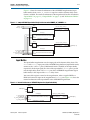
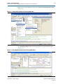
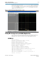
3–4
Chapter 3: Functional Description
Design Example 1: Dynamically Changing Delay Chains in Output Buffer of Stratix III Devices
When dynamic delay chains are enabled, two key primitives are used together with
the IO_OBUF primitive (output buffer). They are the IO_CONFIG primitive and the
DELAY_CHAIN primitive. The IO_CONFIG primitive functions to control the
configuration of the necessary delay settings. The necessary delay settings are set into
the respective DELAY_CHAIN primitive that delays the data that passes through the
delay chain based on the delay settings before going through the IO_OBUF primitive
(output buffer).
The design uses the output and output enable (oe) path of the dynamic delay chain,
where both share the same IO_CONFIG settings.
Each of the output and oe delay chains is built from two cascaded output delay cells.
In this case, xxx_dyn_delay_chain1a_0, the first output delay cell’s dataout is
connected to xxx_dyn_delay_chain2a_0, the second output delay cell’s datain, where
xxx represents either the output path or oe path. This is because the parameters
chosen during the megafunction creation are use_out_dynamic_delay_chain1 and
use_out_dynamic_delay_chain2). Note the cascaded nature of the delays.
xxx_dyn_delay_chain1a_0, the first output delay cell’s delayctrlin inputs are 4 bits.
This actually signifies the possible delay settings (taps value) available for this
DELAY_CHAIN primitive, which are 0 to 15 taps. Each taps represents 50 ps of delay.
This allows a total delay value between 50 ps (1 * 50) to 750 ps (15 * 50).
For xxx_dyn_delay_chain2a_0, the second output delay cell’s delayctrlin inputs are
4 bits, but the MSB is tied to 0. This signifies the possible delay settings (taps value)
available for this DELAY_CHAIN primitive, which are 0 to 7 taps. Each taps represents 50
ps of delay. This allows a total delay value between 50 ps (1 * 50) to 350 ps (7 * 50).
Because of the cascaded nature of the two delay chains, the effective delay is the sum
of both DELAY_CHAIN primitives. This is reflected more clearly in the simulation results
later in this chapter.
For xxx_dyn_delay_chain2a_0, the second output delay cell’s dataout, is connected to
the obufa_0 output buffer’s input port for the output path and to the obufa_0 output
buffer’s oe port for the oe path. Note that the output path and the oe path have their
own cascaded delay chains.
Functional Results—Analyzing the Functional Behavior of the Design in
ModelSim-Altera Software
This user guide assumes that you are familiar with using the ModelSim-Altera
software before trying out the design example. If you are unfamiliar with the
ModelSim-Altera software, refer to
www.altera.com/support/software/products/modelsim/mod-modelsim.html.
There are links to topics such as installation, usage, and troubleshooting.
To set up the ModelSim-Altera software, follow these steps:
1. Unzip the ALTIOBUF_ex1_msim.zip file to any working directory on your PC.
2. Start ModelSim-Altera software.
3. On the File menu, click Change Directory.
4. Select the folder in which you unzipped the files.
5. Click OK.
I/O Buffer (ALTIOBUF) Megafunction
User Guide
February 2012 Altera Corporation
Chapter 3: Functional Description
Design Example 1: Dynamically Changing Delay Chains in Output Buffer of Stratix III Devices
3–5
6. On the Tools menu, point to TCL, and click Execute Macro. The Execute Do File
dialog box appears.
7. Select the ALTIOBUF_ex1_msim.do file and click Open. This is a script file for
ModelSim that automates all the necessary settings for the simulation.
8. Verify the results by looking at the Waveform Viewer window.
You can rearrange signals, remove signals, add signals, and change the radix by
modifying the script in ALTIOBUF_ex1_msim.do.
The first part of the simulation, at time before 502288 ps, out_datain and out_dataout
do not have any delays, but at 502288 ps (Cursor 8) to 1054392 ps (Cursor 9),
out_io_config_clkena is asserted for approximately 11 clock cycles.
Because there is a 11-bit shift register in the IO_CONFIG primitive, io_config_clkena is
asserted for 11 clock cycles. When fully loaded, the shift register has its bits arranged
to correspond with the datain’s values:
■
datain values set during the first four clock cycles (this is "b0000"). In this case, is
not relevant because the output buffer does not have an input delay cell.
■
datain values set during the next three clock cycles (this is "b000") for the second
output delay cell (xxx_dyn_delay_chain2a_0); therefore, the total delay is 0 ps ( 0 *
50).
■
datain values set during the last four clock cycles (this is "b0001") for the first
output delay cell (xxx_dyn_delay_chain1a_0); therefore, the total delay is 50 ps
(1*50).
The total effective delay is the sum of both delay chains because the delay chains are
cascaded (0 + 50 = 50 ps).
February 2012
Altera Corporation
I/O Buffer (ALTIOBUF) Megafunction
User Guide
3–6
Chapter 3: Functional Description
Design Example 1: Dynamically Changing Delay Chains in Output Buffer of Stratix III Devices
The delay only takes effect when the out_io_config_update signal is asserted for one
clock cycle at 1101716 ps (Cursor 10). After the signal is de-asserted, the delay from
out_datain at 1250000 ps (Cursor 4) to out_dataout at 1250050 ps (Cursor 7) should
be noticeable, which is 50 ps. This is shown in Figure 3–3.
Figure 3–3. Dynamically Changing the Delay Chain Value to 50 ps
The second part of the simulation, at 1,651,448 ps (cursor 11) to 2,200,393 ps
(cursor 12), out_io_config_clkena is asserted for approximately 11 clock cycles.
Because there is an 11-bit shift register in IO_CONFIG primitive, io_config_clkena is
asserted for 11 clock cycles. When fully loaded, the shift register has its bits arranged
to correspond with the datain’s values:
■
datain values set during the first four clock cycles (this is "b0000"). This is not
relevant in this case because the output buffer does not have an input delay cell.
■
datain values set during the next three clock cycles (this is "b000") for the second
output delay cell (xxx_dyn_delay_chain2a_0); therefore, total delay is 0 ps (0 * 50).
■
datain values set during the last four clock cycles (this is "b1111") for the first
output delay cell (xxx_dyn_delay_chain1a_0); therefore, total delay is 750 ps
(15 * 50).
The total effective delay is the sum of both delay chains, because the delay chains are
cascaded (0 + 750 = 750 ps).
I/O Buffer (ALTIOBUF) Megafunction
User Guide
February 2012 Altera Corporation
Chapter 3: Functional Description
Design Example 1: Dynamically Changing Delay Chains in Output Buffer of Stratix III Devices
3–7
The delay only takes effect when the out_io_config_update signal is asserted for one
clock cycle at 2,249,686 ps (cursor 13). After the signal is de-asserted, the delay from
out_datain at 2,450,000 ps (cursor 14) to out_dataout at 2,450,750 ps (cursor 15) is
750 ps. This is shown in Figure 3–4.
Figure 3–4. Dynamically Changing the Delay Chain Value to 750 ps
The third part of the simulation, at 2,950,173 ps (cursor 16) to 3,499,919 ps (cursor 17),
out_io_config_clkena is asserted for approximately 11 clock cycles.
Because there is an 11-bit shift register in IO_CONFIG primitive, io_config_clkena is
asserted for 11 clock cycles. When fully loaded, the shift register has its bits arranged
to correspond with the datain’s values:
■
datain values set during the first four clock cycles (this is "b0000"). In this case,
this is not relevant because output buffer does not have input delay cells.
■
datain values set during the next three clock cycles (this is "b001") for the second
output delay cell (xxx_dyn_delay_chain2a_0); therefore, total delay is 50 ps
(1 * 50).
■
datain values set during the last four clock cycles (this is "b1111") for the first
output delay cell (xxx_dyn_delay_chain1a_0 ); therefore, total delay is 750 ps
(15* 50).
The total effective delay is the sum of both delay chains, because the delay chains are
cascaded (50 + 750 = 800 ps).
February 2012
Altera Corporation
I/O Buffer (ALTIOBUF) Megafunction
User Guide
3–8
Chapter 3: Functional Description
Design Example 1: Dynamically Changing Delay Chains in Output Buffer of Stratix III Devices
The delay only takes effect when the out_io_config_update signal is asserted for one
clock cycle at 3,549,609 ps (cursor 18). After the signal is deasserted, the delay from
out_datain at 3,750,000 ps (cursor 19) to out_dataout at 3,750,800 ps (cursor 20) is
800 ps. This is shown in Figure 3–5.
Figure 3–5. Dynamically Changing the Delay Chain Value to 800 ps
For the final part of the simulation, at 4,302,377 ps (cursor 21) to 4,851,327 ps (Cursor
22), out_io_config_clkena is asserted for approximately 11 clock cycles.
io_config_clkena is asserted for 11 clock cycles because there is an 11-bit shift register
in IO_CONFIG primitive. When fully loaded, the shift register has its bits arranged to
correspond with the datain’s values:
■
datain values set during the first four clock cycles (this is "b0000"). In this case,
this not relevant because the output buffer does not have an input delay cell.
■
datain values set during the next three clock cycles (this is "b111") for the second
output delay cell (xxx_dyn_delay_chain2a_0); therefore, total delay is 350 ps
(7 * 50).
■
datain values set during the last four clock cycles (this is "b1111") for the first
output delay cell (xxx_dyn_delay_chain1a_0); therefore, total delay is 750 ps
(15 * 50).
The total effective delay is the sum of both delay chains because the delay chains are
cascaded (350 + 750 = 1,100 ps).
I/O Buffer (ALTIOBUF) Megafunction
User Guide
February 2012 Altera Corporation
Chapter 3: Functional Description
Verilog HDL Prototype for the ALTIOBUF Megafunction
3–9
The delay only takes effect when the out_io_config_update signal is asserted for one
clock cycle at 4,901,805 ps (cursor 23). After the signal is deasserted, the delay from
out_datain at 5,150,000 ps (cursor 24) to out_dataout at 5,151,100 ps (Cursor 25) is
1,100 ps. This is shown in Figure 3–6.
Figure 3–6. Dynamically Changing the Delay Chain Value to 1,100 ps
Verilog HDL Prototype for the ALTIOBUF Megafunction
You can locate the following Verilog HDL prototypes in the Verilog Design File (.v)
altera_mf.v in the <Quartus II installation directory>\eda\synthesis directory.
ALTIOBUF_IN
module altiobuf_in
#(parameter intended_device_family = "unused",
parameter enable_bus_hold = "FALSE",
parameter number_of_channels = 1,
parameter use_differential_mode = "FALSE",
parameter use_dynamic_termination_control = "FALSE",
parameter use_in_dynamic_delay_chain = "FALSE",
parameter lpm_type = "altiobuf_in",
parameter lpm_hint = "unused")
(input wire [number_of_channels-1:0]datain,
input wire [number_of_channels-1:0] datain_b,
output wire [number_of_channels-1:0] dataout,
input wire [number_of_channels-1:0]dynamicterminationcontrol,
input wire io_config_clk,
input wire [number_of_channels-1:0] io_config_clkena,
input wire io_config_datain,
input wire io_config_update)/* synthesis syn_black_box=1 */;
endmodule //altiobuf_in
February 2012
Altera Corporation
I/O Buffer (ALTIOBUF) Megafunction
User Guide
3–10
Chapter 3: Functional Description
Verilog HDL Prototype for the ALTIOBUF Megafunction
ALTIOBUF_OUT
module altiobuf_out
#(parameter intended_device_family = "unused",
parameter enable_bus_hold = "FALSE",
parameter left_shift_series_termination_control = "FALSE",
parameter number_of_channels = 1,
parameter open_drain_output = "FALSE",
parameter pseudo_differential_mode = "FALSE",
parameter use_differential_mode = "FALSE",
parameter use_oe = "FALSE",
parameter use_out_dynamic_delay_chain1 = "FALSE",
parameter use_out_dynamic_delay_chain2 = "FALSE",
parameter use_termination_control = "FALSE",
parameter width_ptc = 14,
parameter width_stc = 14,
parameter lpm_type = "altiobuf_out",
parameter lpm_hint = "unused")
(input wire[number_of_channels-1:0]datain,
output wire[number_of_channels-1:0]dataout,
output wire[number_of_channels-1:0]dataout_b,
input wireio_config_clk,
input wire[number_of_channels-1:0]io_config_clkena,
input wireio_config_datain,
input wireio_config_update,
input wire[number_of_channels-1:0]oe,
input wire[number_of_channels-1:0]oe_b,
input wire[width_ptc * number_of_channels1:0]parallelterminationcontrol,
input wire[width_ptc * number_of_channels1:0]parallelterminationcontrol_b,
input wire[width_stc * number_of_channels1:0]seriesterminationcontrol,
input wire[width_stc * number_of_channels1:0]seriesterminationcontrol_b)/* synthesis syn_black_box=1 */;
endmodule //altiobuf_out
ALTIOBUF_BIDIR
module altiobuf_bidir
#(parameter intended_device_family = "unused",
parameter enable_bus_hold = "FALSE",
parameter
parameter
parameter
parameter
parameter
parameter
parameter
parameter
I/O Buffer (ALTIOBUF) Megafunction
User Guide
number_of_channels = 1,
open_drain_output = "FALSE",
use_differential_mode = "FALSE",
use_dynamic_termination_control = "FALSE",
use_in_dynamic_delay_chain = "FALSE",
use_out_dynamic_delay_chain1 = "FALSE",
use_out_dynamic_delay_chain2 = "FALSE",
use_termination_control = "FALSE",
February 2012 Altera Corporation
Chapter 3: Functional Description
VHDL Component Declaration for the ALTIOBUF Megafunction
3–11
parameter width_ptc = 14,
parameter width_stc = 14,
parameter lpm_type = "altiobuf_bidir",
parameter lpm_hint = "unused")
(input wire[number_of_channels-1:0]datain,
inout wire[number_of_channels-1:0]dataio,
inout wire[number_of_channels-1:0]dataio_b,
output wire[number_of_channels-1:0]dataout,
input wire[number_of_channels-1:0]dynamicterminationcontrol,
input wire[number_of_channels-1:0]dynamicterminationcontrol_b,
input wire io_config_clk,
input wire[number_of_channels-1:0]io_config_clkena,
input wire io_config_datain,
input wire io_config_update,
input wire[number_of_channels-1:0]oe,
input wire[number_of_channels-1:0]oe_b,
input wire[width_ptc * number_of_channels1:0]parallelterminationcontrol,
input wire[width_ptc * number_of_channels1:0]parallelterminationcontrol_b,
input wire[width_stc * number_of_channels1:0]seriesterminationcontrol,
input wire[width_stc * number_of_channels1:0]seriesterminationcontrol_b)/* synthesis syn_black_box=1 */;
endmodule //altiobuf_bidir
VHDL Component Declaration for the ALTIOBUF Megafunction
You can locate the following VHDL Design File (.vhd) altera_mf.vhd in the
<Quartus II installation directory>\libraries\vhdl\altera_mf directory.
ALTIOBUF_IN
component altiobuf_in
generic (
intended_device_family
:string := "unused";
enable_bus_hold:string := "FALSE";
number_of_channels:natural;
use_differential_mode:string := "FALSE";
use_dynamic_termination_control:string := "FALSE";
use_in_dynamic_delay_chain:string := "FALSE";
lpm_hint:string := "UNUSED";
lpm_type:string := "altiobuf_in");
port(datain:in std_logic_vector(number_of_channels-1 downto 0);
datain_b:in std_logic_vector(number_of_channels-1 downto 0) := (others
=> '0');
February 2012
Altera Corporation
I/O Buffer (ALTIOBUF) Megafunction
User Guide
3–12
Chapter 3: Functional Description
VHDL Component Declaration for the ALTIOBUF Megafunction
dataout:out std_logic_vector(number_of_channels-1 downto 0);
dynamicterminationcontrol:in std_logic_vector(number_of_channels-1
downto 0) := (others => '0');
io_config_clk:in std_logic := '0';
io_config_clkena:in std_logic_vector(number_of_channels-1 downto 0) :=
(others => '0');
io_config_datain:in std_logic := '0';
io_config_update:in std_logic := '0');
end component;
ALTIOBUF_OUT
component altiobuf_out
generic(intended_device_family:string := "unused";
enable_bus_hold:string := "FALSE";
left_shift_series_termination_control:string := "FALSE";
number_of_channels:natural;
open_drain_output:string := "FALSE";
pseudo_differential_mode:string := "FALSE";
use_differential_mode:string := "FALSE";
use_oe:string := "FALSE";
use_out_dynamic_delay_chain1:string := "FALSE";
use_out_dynamic_delay_chain2:string := "FALSE";
use_termination_control:string := "FALSE";
width_ptc:natural := 14;
width_stc:natural := 14;
lpm_hint:string := "UNUSED";
lpm_type:string := "altiobuf_out");
port(datain:in std_logic_vector(number_of_channels-1 downto 0);
dataout:out std_logic_vector(number_of_channels-1 downto 0)
dataout_b:out std_logic_vector(number_of_channels-1 downto 0);
io_config_clk:in std_logic := '0';
io_config_clkena:in std_logic_vector(number_of_channels-1 downto 0) :=
(others => '0');
io_config_datain:in std_logic := '0';
io_config_update:in std_logic := '0'
oe:in std_logic_vector(number_of_channels-1 downto 0) := (others =>
'1');
oe_b:in std_logic_vector(number_of_channels-1 downto 0) := (others =>
'1');
parallelterminationcontrol:in std_logic_vector(width_ptc *
number_of_channels-1 downto 0) := (others => '0');
parallelterminationcontrol_b:in std_logic_vector(width_ptc *
number_of_channels-1 downto 0) := (others => '0');
I/O Buffer (ALTIOBUF) Megafunction
User Guide
February 2012 Altera Corporation
Chapter 3: Functional Description
VHDL Component Declaration for the ALTIOBUF Megafunction
3–13
seriesterminationcontrol:in std_logic_vector(width_stc *
number_of_channels-1 downto 0) := (others => '0');
seriesterminationcontrol_b:in std_logic_vector(width_stc *
number_of_channels-1 downto 0) := (others => '0'));
end component;
ALTIOBUF_BIDIR
component altiobuf_bidir
generic(intended_device_family:string := "unused";
enable_bus_hold:string := "FALSE";
left_shift_series_termination_control:string := "FALSE";
number_of_channels:natural;
open_drain_output:string := "FALSE";
use_differential_mode:string := "FALSE";
use_dynamic_termination_control:string := "FALSE";
use_in_dynamic_delay_chain1:string := "FALSE";
use_in_dynamic_delay_chain2:string := "FALSE";
use_termination_control:string := "FALSE";
width_ptc:natural := 14;
width_stc:natural := 14;
lpm_hint:string := "UNUSED";
lpm_type:string := "altiobuf_out");
port(
datain:in std_logic_vector(number_of_channels-1 downto 0);
dataio:inout std_logic_vector(number_of_channels-1 downto 0);
dataio_b:inout std_logic_vector(number_of_channels-1 downto 0);
dataout:out std_logic_vector(number_of_channels-1 downto 0);
dynamicterminationcontrol:in std_logic_vector(number_of_channels-1
downto 0) := (others => '0');
dynamicterminationcontrol_b:in std_logic_vector(number_of_channels-1
downto 0) := (others => '0');
io_config_clk:in std_logic_vector(number_of_channels-1 downto 0) :=
(others => '0');
io_config_clkena:in std_logic_vector(number_of_channels-1 downto 0) :=
(others => '0');
io_config_datain:in std_logic := '0';
io_config_update:in std_logic := '0'
oe:in std_logic_vector(number_of_channels-1 downto 0);
oe_b:in std_logic_vector(number_of_channels-1 downto 0) := (others =>
'1');
parallelterminationcontrol:in std_logic_vector(width_ptc *
number_of_channels-1 downto 0) := (others => '0');
parallelterminationcontrol_b:in std_logic_vector(width_ptc *
number_of_channels-1 downto 0) := (others => '0');
February 2012
Altera Corporation
I/O Buffer (ALTIOBUF) Megafunction
User Guide
3–14
Chapter 3: Functional Description
Ports and Parameters
seriesterminationcontrol:in std_logic_vector(width_stc *
number_of_channels-1 downto 0) := (others => '0');
seriesterminationcontrol_b:in std_logic_vector(width_stc *
number_of_channels-1 downto 0) := (others => '0');
);
end component;
VHDL LIBRARY-USE Declaration
The VHDL LIBRARY-USE declaration is not required if you use the VHDL
component declaration.
LIBRARY altera_mf;
USE altera_mf.altera_mf_components.all;
Ports and Parameters
The parameter details are only relevant if you bypass the parameter editor and use the
megafunction as a directly parameterized instantiation in your design. The details of
these parameters are hidden from MegaWizard Plug-In Manager interface users. The
options listed in this section describe all of the ports and parameters that are available
to customize the ALTIOBUF megafunction according to your application.
Table 3–3 lists the input ports for the ALTIOBUF megafunction (as input buffer).
Table 3–3. ALTIOBUF Megafunction (As Input Buffer) Input Ports (Part 1 of 2)
Port Name
Required
Description
The input buffer normal data input port.
datain[]
Yes
Input port [NUMBER_OF_CHANNELS - 1..0] wide. The input signal to the I/O output
buffer element. For differential signals, this port acquires the positive signal input.
The negative signal input of a differential signal to the I/O input buffer element.
datain_b[]
No
Input port [NUMBER_OF_CHANNELS - 1..0] wide. When connected, the datain_b port
is always fed by a pad/port atom. This port is used only if the USE_DIFFERENTIAL_MODE
parameter value is TRUE.
Input port that feeds the datain port of IO_CONFIG for user-driven dynamic delay chain.
io_config_
No
datain
Input port used to feed input data to the serial load shift register. The value is a 1-bit wire
shared among all I/O instances. This port is available only if the
USE_IN_DYNAMIC_DELAY_CHAIN parameter value is TRUE.
Input clock port that feeds the IO_CONFIG for user-driven dynamic delay chain.
io_config_
clk
io_config_
clkena[]
Take note that the maximum frequency for this clock is 30 MHz.
No
Input port used as the clock signal of shift register block. The value is a 1-bit wire shared
among all I/O instances. This port is available only if the USE_IN_DYNAMIC_DELAY_CHAIN
parameter value is TRUE.
Input clock-enable that feeds the ena port of IO_CONFIG for user-driven dynamic delay
chain.
No
I/O Buffer (ALTIOBUF) Megafunction
User Guide
Input port [NUMBER_OF_CHANNELS - 1..0] wide. Input port used as the clock enable
signal of the shift register block. This port is available only if the
USE_IN_DYNAMIC_DELAY_CHAIN parameter value is TRUE.
February 2012 Altera Corporation
Chapter 3: Functional Description
Ports and Parameters
3–15
Table 3–3. ALTIOBUF Megafunction (As Input Buffer) Input Ports (Part 2 of 2)
Port Name
Required
Description
Input port that feeds the IO_CONFIG update port for user-driven dynamic delay chain.
io_config_
When asserted, the serial load shift register bits feed the parallel load register. The value is
a 1-bit wire shared among all I/O instances. This port is available only if the
USE_IN_DYNAMIC_DELAY_CHAIN parameter value is TRUE.
No
update
Input signal for bidirectional I/Os.
dynamicterminat
ion
Input port [NUMBER_OF_CHANNELS - 1..0] wide. When specified, this port selects from
the core either Rs code, when the input value is LOW; or Rt code, when the input value is
HIGH. Enable Rt only when the bidirectional I/O is receiving input. When the bidirectional
I/O is not receiving input, disable this port for optimal output performance and power
dissipation.
No
control[]
Value
Rs Code
Rt Code
0
1
0
1
0
1
Table 3–4 shows the output ports for the ALTIOBUF megafunction (as input buffer).
Table 3–4. ALTIOBUF Megafunction (As Input Buffer) Output Ports
Port Name
Required
Description
Input buffer output port.
Yes
dataout[]
Input port [NUMBER_OF_CHANNELS - 1..0] wide. The I/O input buffer element
output.
Table 3–5 shows the parameters for the ALTIOBUF megafunction (as input buffer).
Table 3–5. ALTIOBUF Megafunction (As Input Buffer) Parameters
Port Name
ENABLE_BUS_HOLD
Required
No
Type
String
Comments
Specifies whether the bus hold circuitry is enabled. Values are
TRUE and FALSE. When set to TRUE, bus hold circuitry is
enabled and the previous value, instead of high impedance, is
assigned to the output port when there is no valid input. If
omitted, the default is FALSE.
Note: Currently, ENABLE_BUS_HOLD and
USE_DIFFERENTIAL_MODE cannot be used simultaneously.
USE_DIFFERENTIAL_MODE
No
String
Specifies whether the input buffer is differential. Values are TRUE
and FALSE. When set to TRUE, the output is the difference
between the datain and datain_b ports. If omitted, the default
is FALSE.
Note: Currently, ENABLE_BUS_HOLD and
USE_DIFFERENTIAL_MODE cannot be used simultaneously.
USE_IN_DYNAMIC_
DELAY_CHAIN
February 2012
Altera Corporation
No
String
Specifies whether the input buffer incorporates the user-driven
dynamic delay chain in the megafunction, specifically,
IO_CONFIG and an input delay cell. Values are TRUE and FALSE.
If omitted, the default is FALSE.
I/O Buffer (ALTIOBUF) Megafunction
User Guide
3–16
Chapter 3: Functional Description
Ports and Parameters
Table 3–5. ALTIOBUF Megafunction (As Input Buffer) Parameters
Port Name
Required
NUMBER_OF_
CHANNELS
USE_DYNAMIC_TERMINATI
ON_CONTROL
Type
Comments
Yes
Integer
Specifies the number of I/O buffers that must be instantiated.
Value must be greater than or equal to 1. A value of 1 indicates
that the buffer is a 1-bit port and accommodates wires; a value
greater than 1 indicates that the port can be connected to a bus
of width NUMBER_OF_CHANNELS.
No
String
Specifies dynamic termination control. Values are True and
False. If omitted, the default is False.
Table 3–6 shows the input ports for the ALTIOBUF megafunction (as output buffer).
Table 3–6. ALTIOBUF Megafunction (As Output Buffer) Input Ports (Part 1 of 2)
Port Name
Required
Description
The output buffer input port.
datain[]
Yes
Input port [NUMBER_OF_CHANNELS - 1..0] wide. For differential signals,
this port supplies the positive signal input. Inputs are fed to the I/O output
buffer element.
Input port that feeds the datain port of IO_CONFIG for user-driven dynamic
delay chain.
io_config_datain
No
Input port used to feed input data to the serial load shift register. The value is
a 1-bit wire shared among all I/O instances. This port is available when the:
USE_OUT_DYNAMIC_DELAY_CHAIN1 or USE_OUT_DYNAMIC_DELAY_CHAIN2
parameter value is TRUE.
Input clock port that feeds the IO_CONFIG for user-driven dynamic delay
chain.
Note that the maximum frequency for this clock is 30 MHz.
io_config_clk
No
Input port used as the clock signal of shift register block. The value is a 1-bit
wire shared among all I/O instances. This port is available only if the
USE_OUT_DYNAMIC_DELAY_CHAIN1, or
USE_OUT_DYNAMIC_DELAY_CHAIN2 parameter value is TRUE.
Input clock-enable that feeds the ena port of IO_CONFIG for user-driven
dynamic delay chain.
io_config_clkena[]
No
Input port [NUMBER_OF_CHANNELS - 1..0] wide. Input port used as the
clock signal of shift register block. This port is available only if the
USE_OUT_DYNAMIC_DELAY_CHAIN1 or
USE_OUT_DYNAMIC_DELAY_CHAIN2 parameter value is TRUE.
Input port that feeds the IO_CONFIG update port for user-driven dynamic
delay chain.
io_config_update
No
When asserted, the serial load shift register bits feed the parallel load
register. The value is a 1-bit wire shared among all I/O instances. This port is
available only if the USE_OUT_DYNAMIC_DELAY_CHAIN1 or
USE_OUT_DYNAMIC_DELAY_CHAIN2 parameter value is TRUE.
The output-enable source to the tri-state buffer.
oe[]
I/O Buffer (ALTIOBUF) Megafunction
User Guide
No
Input port [NUMBER_OF_CHANNELS - 1..0] wide. When the oe port is
asserted, dataout and dataout_b are enabled. When oe is de-asserted,
both dataout and dataout_b are disabled. This port is used only when the
USE_OE parameter value is TRUE. If omitted, the default is VCC..
February 2012 Altera Corporation
Chapter 3: Functional Description
Ports and Parameters
3–17
Table 3–6. ALTIOBUF Megafunction (As Output Buffer) Input Ports (Part 2 of 2)
Port Name
Required
Description
The output-enable source to the tri-state buffer.
No
oe_b
Input port [NUMBER_OF_CHANNELS - 1..0] wide. When the oe port is
asserted, dataout and dataout_b are enabled. When oe is de-asserted,
both dataout and dataout_b are disabled. This port is used only when the
USE_DIFFERENTIAL_MODE parameter value is TRUE. If omitted, the default
is VCC..
Receives the current state of the pull up and pull down Rs control buses
from a termination logic block.
seriestermination
No
control[]
Input port [WIDTH_STC * NUMBER_OF_CHANNELS - 1..0] wide. Port is
available only when the USE_TERMINATION_CONTROL parameter value is
TRUE.
Receives the current state of the pull up and pull down Rs control buses
from a termination logic block.
seriestermination
No
control_b
Input port [WIDTH_STC * NUMBER_OF_CHANNELS - 1..0] wide. Port is
available only when the USE_DIFFERENTIAL_MODE parameter value is
TRUE.
Receives the current state of the pull up and pull down Rt control buses
from a termination logic block.
parallelterminationcont
rol[]
No
Input port [WIDTH_PTC * NUMBER_OF_CHANNELS - 1..0] wide. Port is
available only when the USE_TERMINATION_CONTROL parameter value is
TRUE. The port is available for Stratix III device families only. Supported in
Stratix® series only.
Receives the current state of the pull up and pull down Rt control buses
from a termination logic block.
parallelterminationcont
rol_b
No
Input port [WIDTH_PTC * NUMBER_OF_CHANNELS - 1..0] wide. Port is
available only when the USE_DIFFERENTIAL_MODE parameter value is
TRUE. The port is available for Stratix III device families only. Supported in
Stratix series only.
Table 3–7 shows the output ports for the ALTIOBUF megafunction (as output buffer).
Table 3–7. ALTIOBUF Megafunction (As Output Buffer) Output Ports
Port Name
Required
Description
Output buffer output port.
Yes
dataout[]
Output port [NUMBER_OF_CHANNELS - 1..0] wide. The I/O output buffer element
output.
Differential output buffer-negative output.
dataout_b[]
February 2012
No
Altera Corporation
Output port [NUMBER_OF_CHANNELS - 1..0] wide. The I/O output buffer negative
output. Port is applicable only when the USE_DIFFERENTIAL_MODE parameter value is
TRUE.
I/O Buffer (ALTIOBUF) Megafunction
User Guide
3–18
Chapter 3: Functional Description
Ports and Parameters
Table 3–8 shows the parameters for the ALTIOBUF megafunction (as output buffer).
Table 3–8. ALTIOBUF Megafunction (As Output Buffer) Parameter (Part 1 of 2)
Port Name
ENABLE_BUS_HOLD
Required
No
Type
String
Description
Specifies whether the bus hold circuitry is enabled. Values are
TRUE and FALSE. When set to TRUE, bus hold circuitry is
enabled, and the previous value, instead of high impedance, is
assigned to the output port when there is no valid input. If
omitted, the default is FALSE.
Note: Currently, ENABLE_BUS_HOLD and
USE_DIFFERENTIAL_MODE cannot be used simultaneously.
USE_DIFFERENTIAL_MOD
E
OPEN_DRAIN_
OUTPUT
USE_TERMINATION_
CONTROL
USE_OUT_DYNAMIC_
DELAY_CHAIN1
USE_OUT_DYNAMIC_
DELAY_CHAIN2
No
String
Specifies whether the output buffer mode is differential. Values
are TRUE and FALSE. When set to TRUE, both the dataout and
dataout_b ports are used. If omitted, the default is FALSE.
Note: Currently, ENABLE_BUS_HOLD and
USE_DIFFERENTIAL_MODE cannot be used simultaneously.
No
No
No
No
String
Open drain mode. Values are TRUE and FALSE. If omitted, the
default is FALSE.
Note: Currently, OPEN_DRAIN_OUTPUT and
USE_DIFFERENTIAL_MODE cannot be used simultaneously.
String
Specifies series termination control and parallel termination
control. Values are TRUE and FALSE. If omitted, the default is
FALSE. When this parameter is used for Arria II GX devices and
the Cyclone series, only series termination control is available.
Stratix series support both.
String
Specifies whether the output buffer incorporates a user-driven
dynamic delay chain in the megafunction, specifically,
IO_CONFIG and the first output delay cell. Additional input ports
are io_config_clk, io_config_clkena, io_config_update,
and io_config_datain. Values are TRUE and FALSE. If
omitted, the default is FALSE.
String
Specifies whether the output buffer incorporates a user-driven
dynamic delay chain in the megafunction, specifically,
IO_CONFIG and the second output delay cell. Additional input
ports are io_config_clk, io_config_clkena,
io_config_update, and io_config_datain. Values are TRUE
and FALSE. If omitted, the default is FALSE.
NUMBER_OF_
CHANNELS
Yes
Integer
Specifies the number of I/O buffers that must be instantiated.
Value must be greater than or equal to 1. A value of 1 indicates
that the buffer is a 1-bit port and accommodates wires. A value
greater than 1 indicates that the port can be connected to a bus of
width NUMBER_OF_CHANNELS.
WIDTH_STC
No
Integer
Specifies the width setting for the series termination control bus.
WIDTH_PTC
No
Integer
Specifies the width setting for the parallel termination control
bus.
USE_OE
No
String
Specifies whether the oe port is used.
I/O Buffer (ALTIOBUF) Megafunction
User Guide
February 2012 Altera Corporation
Chapter 3: Functional Description
Ports and Parameters
3–19
Table 3–8. ALTIOBUF Megafunction (As Output Buffer) Parameter (Part 2 of 2)
Port Name
Required
Type
Description
LEFT_SHIFT_SERIES_TE
RMINATION_CONTROL
No
String
Values are True and False. If omitted, the default is False.
Available for all supported devices except Cyclone series device
family.
PSEUDO_DIFFERENTIAL_
MODE
No
String
Specifies the pseudo differential mode. Values are True and
False. If omitted, the default is False. Available only when the
USE_DIFFERENTIAL_MODE parameter value is TRUE.
Table 3–9 shows the input ports for the ALTIOBUF megafunction (as bidirectional
buffer), Table 3–10 shows the output ports for ALTIOBUF megafunction (as
bidirectional buffer), Table 3–11 shows the bidirectional ports for ALTIOBUF
megafunction (as bidirectional buffer), and Table 3–12 shows the parameters for
ALTIOBUF megafunction (as bidirectional buffer).
Table 3–9. ALTIOBUF Megafunction (As Bidirectional Buffer) Input Ports (Part 1 of 2)
Port Name
Required
Description
The input buffer input port.
Yes
datain[]
Input port [NUMBER_OF_CHANNELS - 1..0] wide. The input signal to the
I/O output buffer element.
Input port that feeds the datain port of IO_CONFIG for user-driven dynamic
delay chain.
io_config_datain
No
Input port used to feed input data to the serial load shift register. The value is
a 1-bit wire shared among all I/O instances. This port is available only if the
USE_IN_DYNAMIC_DELAY_CHAIN, USE_OUT_DYNAMIC_DELAY_CHAIN1, or
USE_OUT_DYNAMIC_DELAY_CHAIN2 parameter value is TRUE.
Input clock port that feeds the IO_CONFIG for user-driven dynamic delay
chain.
Note that the maximum frequency for this clock is 30 MHz.
io_config_clk
No
Input port used as the clock signal of shift register block. The value is a 1-bit
wire shared among all I/O instances. This port is available only if the
USE_IN_DYNAMIC_DELAY_CHAIN, USE_OUT_DYNAMIC_DELAY_CHAIN1, or
USE_OUT_DYNAMIC_DELAY_CHAIN2 parameter value is TRUE.
Input clock-enable that feeds the ena port of IO_CONFIG for user-driven
dynamic delay chain.
io_config_clkena[]
No
Input port [NUMBER_OF_CHANNELS - 1..0] wide. Input port used as the
clock signal of the shift register block. This port is available only if the
USE_IN_DYNAMIC_DELAY_CHAIN, USE_OUT_DYNAMIC_DELAY_CHAIN1, or
USE_OUT_DYNAMIC_DELAY_CHAIN2 parameter value is TRUE.
Input port that feeds the IO_CONFIG update port for user-driven dynamic
delay chain.
io_config_update
No
oe[]
Yes
When asserted, the serial load shift register bits feed the parallel load
register. The value is a 1-bit wire shared among all I/O instances. This port is
available only if the USE_IN_DYNAMIC_DELAY_CHAIN,
USE_OUT_DYNAMIC_DELAY_CHAIN1, or
USE_OUT_DYNAMIC_DELAY_CHAIN2 parameter value is TRUE.
The output-enable source to the tri-state buffer.
February 2012
Altera Corporation
Input port [NUMBER_OF_CHANNELS - 1..0] wide. If omitted, the default is
VCC.
I/O Buffer (ALTIOBUF) Megafunction
User Guide
3–20
Chapter 3: Functional Description
Ports and Parameters
Table 3–9. ALTIOBUF Megafunction (As Bidirectional Buffer) Input Ports (Part 2 of 2)
Port Name
Required
Description
The output-enable source to the tri-state buffer.
oe_b
No
Input port [NUMBER_OF_CHANNELS - 1..0] wide. If omitted, the default is
VCC. Port is available only when the USE_DIFFERENTIAL_MODE parameter
value is TRUE.
Input signal for bidirectional I/Os.
dynamictermination
control[]
No
Input port [NUMBER_OF_CHANNELS - 1..0] wide. When specified, this
port selects from the core either Rs code, when the input value is LOW; or
Rt code, when the input value is HIGH. Enable Rt only when the bidirectional
I/O is receiving input. When the bidirectional I/O is not receiving input,
disable this port for optimal output performance and power dissipation.
Value
Rs Code
Rt Code
0
1
0
1
0
1
Input signal for bidirectional I/Os.
dynamictermination
control_b
seriestermination
control[]
seriestermination
control_b
parallelterminationcont
rol[]
No
No
No
Input port [NUMBER_OF_CHANNELS - 1..0] wide. When specified, this
port selects from the core either Rs code, when the input value is LOW; or
Rt code, when the input value is HIGH. Enable Rt only when the bidirectional
I/O is receiving input. When the bidirectional I/O is not receiving input,
disable this port for optimal output performance and power dissipation. Port
is available only when the USE_DIFFERENTIAL_MODE parameter value is
TRUE.
Value
Rs Code
Rt Code
0
1
0
1
0
1
Receives the current state of the pull up and pull down Rs control buses
from a termination logic block.
[WIDTH_STC * NUMBER_OF_CHANNELS - 1..0] wide. Port is applicable
only when the USE_TERMINATION_CONTROL parameter value is TRUE.
Receives the current state of the pull up and pull down Rs control buses
from a termination logic block.
[WIDTH_STC * NUMBER_OF_CHANNELS - 1..0] wide. Port is applicable
only when the USE_TERMINATION_CONTROL parameter value is TRUE.
Receives the current state of the pull up and pull down Rt control buses
from a termination logic block.
No
Input port [((WIDTH_PTC * NUMBER_OF_CHANNELS) - 1)..0] wide.
Port is applicable only when the USE_TERMINATION_CONTROL parameter
value is TRUE.
Receives the current state of the pull up and pull down Rt control buses
from a termination logic block.
parallelterminationcont
rol_b
I/O Buffer (ALTIOBUF) Megafunction
User Guide
No
Input port [((WIDTH_PTC * NUMBER_OF_CHANNELS) - 1)..0] wide.
Port is applicable only when the USE_TERMINATION_CONTROL parameter
value is TRUE.
February 2012 Altera Corporation
Chapter 3: Functional Description
Ports and Parameters
3–21
Table 3–10. ALTIOBUF Megafunction (As Bidirectional Buffer) Output Ports
Port Name
Required
Description
Buffer output port.
Yes
dataout[]
Output port [NUMBER_OF_CHANNELS - 1..0] wide. The I/O output buffer element
output.
Table 3–11. ALTIOBUF Megafunction (As Bidirectional Buffer) Bidirectional Ports
Port Name
Required
Yes
dataio[]
Description
Bidirectional port that directly feeds a bidirectional pin in the top-level design.
Bidirectional port [(NUMBER_OF_CHANNELS - 1)..0] wide.
Bidirectional DDR port that directly feeds a bidirectional pin in the top-level design.
No
dataio_b[]
Bidirectional port [(NUMBER_OF_CHANNELS - 1)..0] wide. The negative signal
input/output to/from the I/O buffer. This port is used only if the
use_differential_mode_parameter is set to TRUE.
Table 3–12. ALTIOBUF Megafunction(As Bidirectional Buffer) Parameter (Part 1 of 2)
Port Name
ENABLE_BUS_HOLD
Required
No
Type
String
Description
Specifies whether the bus hold circuitry is enabled. Values are
TRUE and FALSE. When set to TRUE, bus hold circuitry is
enabled, and the previous value, instead of high impedance, is
assigned to the output port when there is no valid input. If
omitted, the default is FALSE.
Note: Currently, ENABLE_BUS_HOLD and
USE_DIFFERENTIAL_MODE cannot be used simultaneously.
USE_
DIFFERENTIAL_
MODE
OPEN_DRAIN_ OUTPUT
USE_TERMINATION_CONTROL
USE_DYNAMIC_
TERMINATION_
CONTROL
February 2012
Altera Corporation
No
String
Specifies whether the bidirectional buffer is differential. Values
are TRUE and FALSE. When set to TRUE, the output is the
difference between the dataio and dataio_b ports. If omitted,
the default is FALSE.
Note: Currently, ENABLE_BUS_HOLD and
USE_DIFFERENTIAL_MODE cannot be used simultaneously.
No
No
String
String
Open drain mode. Values are TRUE and FALSE. If omitted, the
default is FALSE.
OPEN_DRAIN_OUTPUT and USE_DIFFERENTIAL_MODE cannot be
used simultaneously.
Specifies series termination control and parallel termination
control. Values are TRUE and FALSE. If omitted, the default is
FALSE. When this parameter is used for Arria II GX devices and
Cyclone series, only series termination control is available. Stratix
series supports both.
Specifies dynamic termination control. Values are TRUE and
FALSE. If omitted, the default is FALSE.
No
String
An error is issued if parallel termination (Rt) is on and dynamic
termination control is not connected on a bidir pin. An error is
issued if Rt is off and dynamic termination control is connected
on an input or bidirectional pin.
I/O Buffer (ALTIOBUF) Megafunction
User Guide
3–22
Chapter 3: Functional Description
Ports and Parameters
Table 3–12. ALTIOBUF Megafunction(As Bidirectional Buffer) Parameter (Part 2 of 2)
Port Name
USE_IN_DYNAMIC_DELAY_CH
AIN
USE_OUT_DYNAMIC_DELAY_C
HAIN1
USE_OUT_DYNAMIC_DELAY_C
HAIN2
Required
No
No
No
Type
Description
String
Specifies whether the input buffer incorporates the user-driven
dynamic delay chain in the megafunction, specifically,
IO_CONFIG and an input delay cell. Additional input ports are
io_config_clk, io_config_clkena, io_config_update,
and io_config_datain. Values are TRUE and FALSE. If
omitted, the default is FALSE.
String
Specifies whether the output buffer incorporates a user-driven
dynamic delay chain in the megafunction, specifically,
IO_CONFIG and the first output delay cell. Additional input ports
are io_config_clk, io_config_clkena, io_config_update,
and io_config_datain. Values are TRUE and FALSE. If
omitted, the default is FALSE.
String
Specifies whether the output buffer incorporates a user-driven
dynamic delay chain in the megafunction, specifically,
IO_CONFIG and the second output delay cell. Additional input
ports are io_config_clk, io_config_clkena,
io_config_update, and io_config_datain. Values are TRUE
and FALSE. If omitted, the default is FALSE.
NUMBER_OF_
CHANNELS
Yes
Integer
Specifies the number of I/O buffers that must be instantiated.
Value must be greater than or equal to 1. A value of 1 indicates
that the buffer is a 1-bit port and accommodates wires. A value
greater than 1 indicates that the port can be connected to a bus of
width NUMBER_OF_CHANNELS.
WIDTH_STC
No
Integer
Specifies the width setting for the series termination control bus.
WIDTH_PTC
No
Integer
Specifies the width setting for the parallel termination control
bus.
I/O Buffer (ALTIOBUF) Megafunction
User Guide
February 2012 Altera Corporation
Additional Information
This chapter provides additional information about the document and Altera.
Document Revision History
The following table lists the revision history for this user guide.
Date
Version
February 2012
November 2010
December 2008
November 2007
3.0
2.1
2.0
1.0
Changes
■
Updated device support
■
Added references to device handbook for delay chain values
■
Updated to new template
■
Updated ports and parameters
■
Added prototypes and component declarations
■
Added sentence to I/O Buffer and Dynamic Delay Integration
■
Added two last paragraph to Common Applications
■
Added extra note to Table 3–5
■
Remove figures
Initial Release.
How to Contact Altera
To locate the most up-to-date information about Altera products, refer to the
following table.
Contact (1)
Technical support
Technical training
Product literature
Contact Method
Address
Website
www.altera.com/support
Website
www.altera.com/training
Email
Website
[email protected]
www.altera.com/literature
Nontechnical support (general)
Email
[email protected]
(software licensing)
Email
[email protected]
Note to Table:
(1) You can also contact your local Altera sales office or sales representative.
February 2012
Altera Corporation
I/O Buffer (ALTIOBUF) Megafunction
User Guide
Info–2
Additional Information
Typographic Conventions
The following table shows the typographic conventions this document uses.
Visual Cue
Meaning
Bold Type with Initial Capital
Letters
Indicate command names, dialog box titles, dialog box options, and other GUI
labels. For example, Save As dialog box. For GUI elements, capitalization matches
the GUI.
bold type
Indicates directory names, project names, disk drive names, file names, file name
extensions, software utility names, and GUI labels. For example, \qdesigns
directory, D: drive, and chiptrip.gdf file.
Italic Type with Initial Capital Letters
Indicate document titles. For example, Stratix IV Design Guidelines.
Indicates variables. For example, n + 1.
italic type
Variable names are enclosed in angle brackets (< >). For example, <file name> and
<project name>.pof file.
Initial Capital Letters
Indicate keyboard keys and menu names. For example, the Delete key and the
Options menu.
“Subheading Title”
Quotation marks indicate references to sections in a document and titles of
Quartus II Help topics. For example, “Typographic Conventions.”
Indicates signal, port, register, bit, block, and primitive names. For example, data1,
tdi, and input. The suffix n denotes an active-low signal. For example, resetn.
Courier type
Indicates command line commands and anything that must be typed exactly as it
appears. For example, c:\qdesigns\tutorial\chiptrip.gdf.
Also indicates sections of an actual file, such as a Report File, references to parts of
files (for example, the AHDL keyword SUBDESIGN), and logic function names (for
example, TRI).
r
An angled arrow instructs you to press the Enter key.
1., 2., 3., and
a., b., c., and so on
Numbered steps indicate a list of items when the sequence of the items is important,
such as the steps listed in a procedure.
■ ■
Bullets indicate a list of items when the sequence of the items is not important.
■
1
The hand points to information that requires special attention.
h
The question mark directs you to a software help system with related information.
f
The feet direct you to another document or website with related information.
?
The multimedia icon directs you to a related multimedia presentation.
c
A caution calls attention to a condition or possible situation that can damage or
destroy the product or your work.
w
A warning calls attention to a condition or possible situation that can cause you
injury.
The envelope links to the Email Subscription Management Center page of the Altera
website, where you can sign up to receive update notifications for Altera documents.
I/O Buffer (ALTIOBUF) Megafunction
User Guide
February 2012 Altera Corporation