1
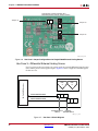
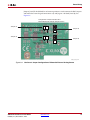
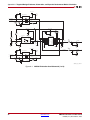
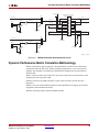
AMS101 Evaluation
Card
User Guide
UG886 (v1.3) November 6, 2013
DISCLAIMER
The information disclosed to you hereunder (the “Materials”) is provided solely for the selection and use of Xilinx products. To the maximum
extent permitted by applicable law: (1) Materials are made available "AS IS" and with all faults, Xilinx hereby DISCLAIMS ALL
WARRANTIES AND CONDITIONS, EXPRESS, IMPLIED, OR STATUTORY, INCLUDING BUT NOT LIMITED TO WARRANTIES OF
MERCHANTABILITY, NON-INFRINGEMENT, OR FITNESS FOR ANY PARTICULAR PURPOSE; and (2) Xilinx shall not be liable (whether
in contract or tort, including negligence, or under any other theory of liability) for any loss or damage of any kind or nature related to, arising
under, or in connection with, the Materials (including your use of the Materials), including for any direct, indirect, special, incidental, or
consequential loss or damage (including loss of data, profits, goodwill, or any type of loss or damage suffered as a result of any action
brought by a third party) even if such damage or loss was reasonably foreseeable or Xilinx had been advised of the possibility of the same.
Xilinx assumes no obligation to correct any errors contained in the Materials or to notify you of updates to the Materials or to product
specifications. You may not reproduce, modify, distribute, or publicly display the Materials without prior written consent. Certain products are
subject to the terms and conditions of Xilinx’s limited warranty, please refer to Xilinx’s Terms of Sale which can be viewed at
http://www.xilinx.com/legal.htm#tos; IP cores may be subject to warranty and support terms contained in a license issued to you by Xilinx.
Xilinx products are not designed or intended to be fail-safe or for use in any application requiring fail-safe performance; you assume sole risk
and liability for use of Xilinx products in such critical applications, please refer to Xilinx’s Terms of Sale which can be viewed at
http://www.xilinx.com/legal.htm#tos.
Automotive Applications Disclaimer
XILINX PRODUCTS ARE NOT DESIGNED OR INTENDED TO BE FAIL-SAFE, OR FOR USE IN ANY APPLICATION REQUIRING
FAIL-SAFE PERFORMANCE, SUCH AS APPLICATIONS RELATED TO: (I) THE DEPLOYMENT OF AIRBAGS, (II) CONTROL OF A
VEHICLE, UNLESS THERE IS A FAIL-SAFE OR REDUNDANCY FEATURE (WHICH DOES NOT INCLUDE USE OF SOFTWARE IN THE
XILINX DEVICE TO IMPLEMENT THE REDUNDANCY) AND A WARNING SIGNAL UPON FAILURE TO THE OPERATOR, OR (III) USES
THAT COULD LEAD TO DEATH OR PERSONAL INJURY. CUSTOMER ASSUMES THE SOLE RISK AND LIABILITY OF ANY USE OF
XILINX PRODUCTS IN SUCH APPLICATIONS.
© Copyright 2012–2013 Xilinx, Inc. Xilinx, the Xilinx logo, Artix, ISE, Kintex, Spartan, Virtex, Vivado, Zynq, and other designated brands
included herein are trademarks of Xilinx in the United States and other countries. All other trademarks are the property of their respective
owners.
Revision History
The following table shows the revision history for this document.
Date
Version
Revision
07/16/2012
1.0
Initial Xilinx release.
10/19/2012
1.1
Section AMS101 Evaluation Card Overview, page 7 explains that reference designs are
now supplied for the ZC702, KC705, and VC707 base boards, and how to download
the designs. Cable terminology changed to Standard-A plug to Mini-B plug USB cable
and Standard-A plug to Micro-B plug USB cable, and these two cables are added to the
kit. Board drawings and photographs in Figure 1-2 and Figure 1-2 were updated.
Procedures in Hardware and Software Setup, page 12 were updated. Figure 2-4,
Figure 2-5, and Figure 2-9 were updated. The AMS102 characterization card was
removed. In Analyze Internal Voltage and Temperature Sensors, page 24, Open is
replaced with Select. Figure 3-4 and Figure 3-6 were replaced. In Appendix B,
Required Jumper Settings for Base Boards, a note was added that the triangle
represents pin 1. Jumper J65 on the ZC702 board changed to In place. Some references
in the book and in Appendix C, Additional Resources changed. Appendix D, Regulatory
and Compliance Information now includes a link to the Declaration of Conformity and
markings for waste electrical and electronic equipment (WEEE), restriction of hazardous
substances (RoHS), and CE compliance.
AMS101 Evaluation Card User Guide
www.xilinx.com
UG886 (v1.3) November 6, 2013
Date
Version
02/14/2013
1.2
Revision
Chapter 1, AMS101 Evaluation Card Overview: Instances of AMS101 evaluator tool
were corrected to AMS evaluator tool. Added part HW-AMS101-G. Reference design
files are now downloaded from
www.xilinx.com/support/documentation/ams101_evaluation_card.htm. The AC701
board is now supported. The bullet with “AMS evaluator tool graphical user
interface” was removed from section AMS101 Evaluation Card, page 7. Download
information for the AMS evaluator tool graphical user interface is listed in the last
bullet on page 7 and the bullet about “FPGA programming files...” was removed.
Chapter 2, AMS101 Evaluation Card Quick Start: The onboard signal source is from a
16-bit dual DAC, page 11. In step 1, page 12, download information changed. In
step 7, page 16, the AC701 kit and kit documentation references were added.
Various changes were added to step 9, page 18. Added section Power Monitoring
with XADC on AC701, page 24.
Chapter 4, AMS Evaluator Tool: Decimation information and Table 4-2 were added on
page 44.
Appendix A, Targeted Design Platforms, Schematics, and Dynamic Performance Metric
Calculation Methodology: AC701 was added to the Supported Targeted Design
Platforms section.
Appendix B, Required Jumper Settings for Base Boards: Added Jumper Settings for the
AC701 Board, page 52.
11/06/2013
1.3
UG886 (v1.3) November 6, 2013
Updated for Vivado® Design Suite 2013.3. Procedures in step 7, page 16 were revised for
the Vivado tool and the KC705 ZIP file name changed. Support for Zynq®-7000 ZC706
AP SoC was added in Jumper Settings for the ZC706 Board, page 52. Updated
Appendix C, Additional Resources links. The link to the Declaration of Conformity,
page 55 was updated.
www.xilinx.com
AMS101 Evaluation Card User Guide
AMS101 Evaluation Card User Guide
www.xilinx.com
UG886 (v1.3) November 6, 2013
Table of Contents
Revision History . . . . . . . . . . . . . . . . . . . . . . . . . . . . . . . . . . . . . . . . . . . . . . . . . . . . . . . . . . . . . 2
Chapter 1: AMS101 Evaluation Card Overview
Overview . . . . . . . . . . . . . . . . . . . . . . . . . . . . . . . . . . . . . . . . . . . . . . . . . . . . . . . . . . . . . . . . . . . . 7
Chapter 2: AMS101 Evaluation Card Quick Start
Quick Start . . . . . . . . . . . . . . . . . . . . . . . . . . . . . . . . . . . . . . . . . . . . . . . . . . . . . . . . . . . . . . . . .
Run Key Performance Tests . . . . . . . . . . . . . . . . . . . . . . . . . . . . . . . . . . . . . . . . . . . . . . . . .
Analyze Internal Voltage and Temperature Sensors . . . . . . . . . . . . . . . . . . . . . . . . . .
Power Monitoring with XADC on AC701 . . . . . . . . . . . . . . . . . . . . . . . . . . . . . . . . . . . .
12
21
24
24
Chapter 3: AMS101 Evaluation Hardware
Interfacing to the FPGA Base Board . . . . . . . . . . . . . . . . . . . . . . . . . . . . . . . . . . . . . . . . . 30
Board Setup . . . . . . . . . . . . . . . . . . . . . . . . . . . . . . . . . . . . . . . . . . . . . . . . . . . . . . . . . . . . . . . . . 31
Chapter 4: AMS Evaluator Tool
XADC Configuration . . . . . . . . . . . . . . . . . . . . . . . . . . . . . . . . . . . . . . . . . . . . . . . . . . . . . . . . 38
XADC Performance Tests . . . . . . . . . . . . . . . . . . . . . . . . . . . . . . . . . . . . . . . . . . . . . . . . . . . 41
AMS Demonstration . . . . . . . . . . . . . . . . . . . . . . . . . . . . . . . . . . . . . . . . . . . . . . . . . . . . . . . . 44
Appendix A: Targeted Design Platforms, Schematics, and Dynamic
Performance Metric Calculation Methodology
Supported Targeted Design Platforms . . . . . . . . . . . . . . . . . . . . . . . . . . . . . . . . . . . . . . . 47
Schematics . . . . . . . . . . . . . . . . . . . . . . . . . . . . . . . . . . . . . . . . . . . . . . . . . . . . . . . . . . . . . . . . . . 47
Dynamic Performance Metric Calculation Methodology . . . . . . . . . . . . . . . . . . . . . 49
Appendix B: Required Jumper Settings for Base Boards
Jumper Settings for the KC705 Board . . . . . . . . . . . . . . . . . . . . . . . . . . . . . . . . . . . . . . . .
Jumper Settings for the VC707 Board . . . . . . . . . . . . . . . . . . . . . . . . . . . . . . . . . . . . . . . .
Jumper Settings for the ZC702 Board . . . . . . . . . . . . . . . . . . . . . . . . . . . . . . . . . . . . . . . .
Jumper Settings for the ZC706 Board . . . . . . . . . . . . . . . . . . . . . . . . . . . . . . . . . . . . . . . .
Jumper Settings for the AC701 Board . . . . . . . . . . . . . . . . . . . . . . . . . . . . . . . . . . . . . . . .
51
51
51
52
52
Appendix C: Additional Resources
Xilinx Resources . . . . . . . . . . . . . . . . . . . . . . . . . . . . . . . . . . . . . . . . . . . . . . . . . . . . . . . . . . . . 53
Solution Centers . . . . . . . . . . . . . . . . . . . . . . . . . . . . . . . . . . . . . . . . . . . . . . . . . . . . . . . . . . . . 53
References . . . . . . . . . . . . . . . . . . . . . . . . . . . . . . . . . . . . . . . . . . . . . . . . . . . . . . . . . . . . . . . . . . 53
AMS101 Evaluation Card User Guide
UG886 (v1.3) November 6, 2013
www.xilinx.com
5
Appendix D: Regulatory and Compliance Information
Declaration of Conformity . . . . . . . . . . . . . . . . . . . . . . . . . . . . . . . . . . . . . . . . . . . . . . . . . .
Directives . . . . . . . . . . . . . . . . . . . . . . . . . . . . . . . . . . . . . . . . . . . . . . . . . . . . . . . . . . . . . . . . . . .
Standards . . . . . . . . . . . . . . . . . . . . . . . . . . . . . . . . . . . . . . . . . . . . . . . . . . . . . . . . . . . . . . . . . . .
Markings . . . . . . . . . . . . . . . . . . . . . . . . . . . . . . . . . . . . . . . . . . . . . . . . . . . . . . . . . . . . . . . . . . .
6
www.xilinx.com
55
55
55
56
AMS101 Evaluation Card User Guide
UG886 (v1.3) November 6, 2013
Chapter 1
AMS101 Evaluation Card Overview
Overview
AMS101 Evaluation Card
The Xilinx 7 series FPGAs and Zynq-7000® All Programmable System on a Chip (AP SoC)
each feature two 1 Mega-sample per second (MSPS), 12-bit, Xilinx analog-to-digital
converters (XADCs) built into the device (FPGA or SoC). The Analog Mixed Signal (AMS)
technology combines the XADC analog measurement with the device’s logic for simple
system monitoring to more signal processing-intensive tasks like linearization, calibration,
oversampling, and filtering. The AMS101 evaluation card (part number HW-AMS101-G)
provides an analog source to verify the XADC and AMS performance. The AMS101
evaluation card plugs into all Xilinx 7 series FPGA and Zynq-7000 AP SoC base boards.
Reference designs are supplied for the ZC702, KC705, AC701, and VC707 base boards.
Download these files from either the individual kit support pages or the AMS101
Evaluation Card website. For convenience, the KC705 FPGA base board is used as the
example in this document (see Figure 1-1). The KC705 evaluation kit includes hardware
and soft content required to evaluate XADC and to determine how it can be useful in the
end system.
To evaluate the Xilinx Analog Mixed Signal (AMS) capability, these items from the kit are
needed:
•
Access to the XADC header (see Figure 1-1)
•
AMS101 evaluation card (see Figure 1-2 and Table 1-1 for a description of features)
•
Two USB cables (1x Standard-A plug to Mini-B plug USB cable and 1x Standard-A
plug to Micro-B plug USB cable for download and debug
•
USB-UART drivers
•
Download AMS reference design files from the AMS101 Evaluation Card website.
•
Download AMS evaluator tool graphical user interface (7 Series FPGA and Zynq-7000
AP SoC AMS Evaluator Installer for AMS Targeted Reference Design—see Figure 1-3).
AMS101 Evaluation Card User Guide
UG886 (v1.3) November 6, 2013
www.xilinx.com
7
Chapter 1: AMS101 Evaluation Card Overview
X-Ref Target - Figure 1-1
AMS101 Evaluation Card
XADC Header (Under AMS101 Card)
UG886_c1_01_091012
Figure 1-1:
KC705 Evaluation Board with the AMS101 Evaluation Card Installed
X-Ref Target - Figure 1-2
1
2
6
5
3
4
UG886_c1_02_020113
Figure 1-2:
8
AMS101 Evaluation Card Features
www.xilinx.com
AMS101 Evaluation Card User Guide
UG886 (v1.3) November 6, 2013
Overview
Table 1-1:
AMS101 Evaluation Card Features
Callout
Component Description
1
Jumpers to select DAC or external signal source.
2
20-pin connector to the XADC header on the FPGA or AP SoC base board.
3
Pins allow for external analog input signals.
4
Digital I/O level translators.
5
16-bit DAC sets analog test voltage.
6
Reference buffer for DAC.
X-Ref Target - Figure 1-3
UG886_c1_03_092512
Figure 1-3:
AMS101 Evaluation Card User Guide
UG886 (v1.3) November 6, 2013
AMS Evaluator Tool GUI
www.xilinx.com
9
Chapter 1: AMS101 Evaluation Card Overview
10
www.xilinx.com
AMS101 Evaluation Card User Guide
UG886 (v1.3) November 6, 2013
Chapter 2
AMS101 Evaluation Card Quick Start
To facilitate easy evaluation of key performance metrics of the XADC and AMS
technology, Xilinx developed the AMS evaluation platform for all 7 series FPGA and
Zynq-7000 AP SoC base boards. The AMS evaluation platform (Figure 2-1) enables key
ADC performance metrics to be observed and evaluated. The remainder of this document
describes in detail the hardware and software that comprise the AMS evaluation platform.
X-Ref Target - Figure 2-1
XADC Header
AMS101
Evaluation
Card
JTAG
UART
USB
FMC (HPC)
KX325TFFG900
1 Gb/s
Ethernet
PHY
PC
KC705 Base Board
PCI Express
Figure 2-1:
FMC (LPC)
UG886_c2_01_101812
AMS Evaluation Platform
AMS Evaluation Platform Features
The AMS evaluation platform provides:
•
A complete XADC and AMS evaluation solution
•
An onboard signal source from a 16-bit dual DAC
•
Configurable analog inputs
•
An interactive GUI
•
Interfaces for all the latest Xilinx FPGA or AP SoC base boards, including the KC705
Kintex-7 FPGA base board, as detailed in this document. (See the full list of supported
base boards in Appendix A).
AMS101 Evaluation Card User Guide
UG886 (v1.3) November 6, 2013
www.xilinx.com
11
Chapter 2: AMS101 Evaluation Card Quick Start
Each base board kit contains:
•
One AMS101 evaluation card
•
USB-UART drivers
•
A base board Getting Started Guide
Quick Start
Eight steps are needed to get the AMS evaluation platform up and running. This chapter
covers how to perform these steps as well as how to run key ADC performance tests after
setup.
Hardware and Software Setup
1.
Install the AMS Evaluator tool GUI.
Download the AMS Evaluator installer files (7 Series FPGA and Zynq-7000 AP SoC AMS
Evaluator Installer for AMS Targeted Reference Design) from the AMS101 Evaluation Card
Support Page. Click the setup.exe file to install the National Instruments LabVIEW
RunTime Engine needed to host the AMS Evaluator tool.
The GUI itself has been built using National Instruments LabVIEW 2011 software. To
enable use of the GUI without the need for a LabVIEW license, Xilinx has bundled the
LabVIEW run-time engine with the GUI installer. During the installation process, the
run time engine is installed on the PC.
2.
Connect the FPGA base board.
Ensure that the FPGA base board power switch (e.g., SW15 on the KC705 base board)
is in the OFF position. Figure 2-2 shows the position of the power switch on the board.
3.
12
Connect the host PC to the UART port with the Standard-A plug to Mini-B plug USB
cable. Also connect the Standard-A plug to Micro-B plug USB cable to the JTAG port.
See the corresponding photo in the Getting Started Guide for each particular base board.
www.xilinx.com
AMS101 Evaluation Card User Guide
UG886 (v1.3) November 6, 2013
Quick Start
X-Ref Target - Figure 2-2
Ensure switch is in OFF position
UG886_c2_02_062712
Figure 2-2:
Power Switch on the FPGA Base Board
Three connections are required for the FPGA base board: power, the USB-UART
connection to the PC, and the JTAG Standard-A plug to Micro-B plug USB
programming cable. Figure 2-3 shows how to connect these on the KC705 base board.
Caution! Do not turn on the power switch until step 6, page 16.
AMS101 Evaluation Card User Guide
UG886 (v1.3) November 6, 2013
www.xilinx.com
13
Chapter 2: AMS101 Evaluation Card Quick Start
X-Ref Target - Figure 2-3
AMS101 Evaluation Card
Board Power
Switch SW12
USB Cable
Standard-A Plug
to Mini-B Plug
To J17
(UART)
Host
Computer
To J18
To JTAG
USB Cable
Standard-A Plug
to Micro-B pPug
Figure 2-3:
Power Supply
100 VAC–240 VAC Input
12 VDC 5.0A Output
UG886_c2_03_091012
FPGA Base Board Connectivity
4.
Configure the FPGA base board jumper settings as listed in Appendix B, Required
Jumper Settings for Base Boards.
5.
Connect the AMS101 evaluation card to the XADC header on the base board.
The AMS101 evaluation card connects to the FPGA base board by plugging the card
into the XADC header on the base board. The AMS101 evaluation card connector and
XADC header socket are keyed to align properly. Pin 1 on the XADC header needs to
connect to pin 1 of the 20-pin connector on the AMS101 evaluation card. Figure 2-4
shows this connection.
X-Ref Target - Figure 2-4
XADC Header
AMS101 Evaluation Card
Installed on XADC Header
UG886_c2_04_101812
Figure 2-4:
14
AMS101 Evaluation Card Installed on the Base Board XADC Header
www.xilinx.com
AMS101 Evaluation Card User Guide
UG886 (v1.3) November 6, 2013
Quick Start
Ensure that all the jumper settings are correct on the AMS101 evaluation card. Figure 2-5
shows an example of jumpers J3 and J5 (DACs enabled). Table 2-1 explains additional
jumpers.
Note: The image in Figure 2-5 is for reference only and might not reflect the current revision of the
board.
X-Ref Target - Figure 2-5
1
2
3
7
6
5
2
4
UG886_c2_05_092612
Figure 2-5:
Table 2-1:
AMS101 Evaluation Card Jumper Configuration
AMS101 Evaluation Card Jumper Configuration Notes
Callout
Reference
Designator
Component
Description
1
J2
Jumper
External signal source to VP positive analog input.
Figure A-2, page 49
2
J3
Jumper
1–2 selects DAC signal source.
2–3 selects external input source on J2.
Figure A-2, page 49
20-pin connector to XADC header on FPGA base board.
Figure A-2, page 49
3
Connector
Notes
Schematics
4
J5
Jumper
1–2 selects DAC signal source.
2–3 selects external input source on J6.
Figure A-2, page 49
5
J6
Jumper
External signal source to VN negative analog input.
Figure A-2, page 49
16-bit DAC sets analog test voltage.
Figure A-1, page 48
Reference buffer for DAC.
Figure A-1, page 48
6
DAC
7
Amplifier
AMS101 Evaluation Card User Guide
UG886 (v1.3) November 6, 2013
www.xilinx.com
15
Chapter 2: AMS101 Evaluation Card Quick Start
6.
Power up the FPGA base board.
The power switch can now be put in the ON position (switch toward the power plug).
Figure 2-6 shows the location of the power switch. It also shows the LEDs illuminated
on the FPGA base board. This should occur directly after the FPGA base board switch
is flipped into the ON position. A few seconds after power-up, the DONE LED should
illuminate. At this stage, hardware connection is complete.
X-Ref Target - Figure 2-6
Power Switch
UG886_c2_06_071012
Figure 2-6:
7.
Turning On the FPGA Base Board Power
Download the design to the FPGA. See the individual kit (AC701, ZC702, KC705, or
VC707) Getting Started Guides or the 7 Series FPGA AMS Targeted Reference Design User
Guide (UG960) [Ref 1], for more specific instructions on downloading the design.
For the AMS101 evaluation card to function, the FPGA needs to be programmed with
the appropriate design. To do this, download the design to the FPGA:
a.
Open the Vivado ® Design Suite. Here is one example path for Vivado tools:
Start menu/Xilinx Design Tools/Vivado 2013.3/Vivado 2013.3
b.
Create a Vivado Project.
c.
Open a Hardware Session.
d. Open a new Hardware Target and run through the wizard.
e.
16
Open AMS_KC705_bitstream.bit from the
rdf0280-ams101-kc705-trd-2013-3.zip file.
www.xilinx.com
AMS101 Evaluation Card User Guide
UG886 (v1.3) November 6, 2013
Quick Start
The LEDs on the FPGA base board should light up as the design is downloading.
Figure 2-7 shows an example of the LEDs lit up after the KC705 board is programmed.
X-Ref Target - Figure 2-7
UG886_c2_07_071012
Figure 2-7:
8.
LEDs after Programming the FPGA with the Design
Run the AMS101 evaluator LabVIEW GUI executable file.
If the AMS Evaluator tool GUI was successfully installed, an icon should be displayed
on the desktop and in the Windows start menu (see Figure 2-8). To open the AMS
Evaluator tool GUI, click the red Xilinx X icon. The GUI shown in Figure 2-9 should
appear.
Note: Do not press anything on the GUI until step 9 is performed.
X-Ref Target - Figure 2-8
UG886_c2_08_091012
Figure 2-8:
AMS101 Evaluation Card User Guide
UG886 (v1.3) November 6, 2013
www.xilinx.com
AMS Icon
17
Chapter 2: AMS101 Evaluation Card Quick Start
X-Ref Target - Figure 2-9
Select COM Port Here
UG886_c2_09_092512
Figure 2-9:
9.
AMS Evaluator Tool on Start-Up
Connect to the UART port as detailed in the appropriate FPGA/processor base board
Getting Started Guide:
•
Kintex-7 FPGA KC705 Evaluation Kit Getting Started Guide (UG883) [Ref 2]
•
Getting Started with the Virtex-7 FPGA VC707 Evaluation Kit (UG848) [Ref 3]
•
Zynq-7000 All Programmable SoC: ZC702 Evaluation Kit and Video and Imaging Kit
Getting Started Guide (UG926) [Ref 4]
•
Artix-7 FPGA AC701 Evaluation Kit Getting Started Guide (UG967) [Ref 5]
Set the USB-UART connection to a known port in the Device Manager as follows:
18
•
Right-click My Computer and select Properties.
•
Select the Hardware tab. Click the Device Manager button.
•
Find and right-click the Silicon Labs device in the list. Then select Properties.
•
Click the Port Settings tab and the Advanced... button.
•
Select the COM port that corresponds to Silicon Labs CP210x USB to
UART Bridge (see Figure 2-10).
www.xilinx.com
AMS101 Evaluation Card User Guide
UG886 (v1.3) November 6, 2013
Quick Start
X-Ref Target - Figure 2-10
UG886_c2_10_092512
Figure 2-10:
AMS101 Evaluation Card User Guide
UG886 (v1.3) November 6, 2013
UART-USB Port in Device Manager
www.xilinx.com
19
Chapter 2: AMS101 Evaluation Card Quick Start
Select the appropriate COM port from the pull-down menu on the GUI as show in
Figure 2-11. Then click the Connect button. After the AMS Evaluator tool is connected, the
kit name is displayed below the green Connected circle. If the AMS Evaluator tool is
unable to connect, be sure the correct COM port is selected and click refresh.
X-Ref Target - Figure 2-11
Select COM Port Here
UG886_c2_11_092512
Figure 2-11:
20
AMS Evaluator Tool COM Port Selection
www.xilinx.com
AMS101 Evaluation Card User Guide
UG886 (v1.3) November 6, 2013
Run Key Performance Tests
Run Key Performance Tests
All of the software and hardware should be configured and running. The AMS101
evaluation card can now be used to perform measurement tests on the XADC.
Collect Time Domain Data
To collect time domain data, press the Collect Data button shown in Figure 2-12. A sine
wave should display on the screen. This sine wave has been generated by the
digital-to-analog converter (DAC) on the AMS101 evaluation card and passed through to
the XADC inputs where it was digitized.
X-Ref Target - Figure 2-12
Collect Data Button
UG886_c2_12_092512
Figure 2-12:
AMS101 Evaluation Card User Guide
UG886 (v1.3) November 6, 2013
Run-Time Domain Data Capture
www.xilinx.com
21
Chapter 2: AMS101 Evaluation Card Quick Start
Perform Fast Fourier Transform Analysis
To analyze the performance of the XADC in the frequency domain, select the Frequency
Domain tab (see Figure 2-13). When selected, a Fast Fourier Transform (FFT) is performed
on the XADC data just viewed in the time domain. The signal-to-noise ratio, total
harmonic distortion, effective number of bits (ENOB), and other AC parameters are
calculated and displayed in the data panel below the FFT plot as shown in Figure 2-13. A
new data capture from the XADC can be collected by pressing the Collect Data button.
X-Ref Target - Figure 2-13
Select Frequency Pressing the Collect Data button collects 4,096 XADC data points
Domain tab here and performs an FFT on it.7
FFT AC Data Analyisis
Figure 2-13:
22
UG886_c2_13_092512
Frequency Domain Analysis and Data Capture
www.xilinx.com
AMS101 Evaluation Card User Guide
UG886 (v1.3) November 6, 2013
Run Key Performance Tests
Perform a Linearity Test
To analyze the linearity of the XADC, select the Linearity tab and click the Collect Data
button. After a short wait, both the integral and differential non-linearity data is displayed
on two separate plots along with the minimum and maximum values at the bottom of the
screen as shown in Figure 2-14.
X-Ref Target - Figure 2-14
Perform Linearity Test and Initiate Analog Ramp Output at DAC
UG886_c2_14_092512
Figure 2-14:
AMS101 Evaluation Card User Guide
UG886 (v1.3) November 6, 2013
Linearity Error Data Capture and Analysis
www.xilinx.com
23
Chapter 2: AMS101 Evaluation Card Quick Start
Analyze Internal Voltage and Temperature Sensors
The XADC also has several internal sensors that it digitizes. These include a temperature
sensor and FPGA voltage supply sensors. Select the Sensor Data tab to view the data
corresponding to the four sensors, as shown in Figure 2-15.
X-Ref Target - Figure 2-15
UG886_c2_15_092512
Figure 2-15: Sensor Data Capture
Power Monitoring with XADC on AC701
The AC701 evaluation board and AMS Evaluator tool offer a complete system monitoring
solution. The AC701 uses the XADC to measure voltage and load current on nine of the
onboard power supplies. Voltage is measured using remote sensing. Current is measured
across a sense resistor with individual current sense op amps. Power is then calculated for
each of the nine rails by multiplying voltage x current. An external multiplexer is also used
24
www.xilinx.com
AMS101 Evaluation Card User Guide
UG886 (v1.3) November 6, 2013
Power Monitoring with XADC on AC701
to switch all 18 measurements into the XADC. Table 2-2 details the power rails monitored
on the AC701.
Table 2-2:
AC701 Voltage Rails Measured with AMS Targeted Reference Design
Rail Name
Voltage
Current
(1)
No
Yes
VCCAUX(1)
No
Yes
VCCBRAM(1)
No
Yes
1.5V Supply
Yes
Yes
VCCO_ADJ
Yes
Yes
1.8V Supply
Yes
Yes
3.3V Supply
Yes
Yes
MGTAVCC
Yes
Yes
MGTAVTT
Yes
Yes
VCCINT
Notes:
1. VCCINT, VCCAUX, and VCCBRAM voltage levels are measured by XADC onboard sensors and
displayed in both the Sensor Data tab and the Power Monitor tab.
The current sense values of VCCINT, VCCAUX, VCCBRAM, 1.5V supply, and VCCO_ADJ along
with voltage levels of 1.5V supply, VCCO_ADJ, and 1.8V supply are available on the AC701
board's onboard MUX positioned at U13. The differential output of the MUX is connected
to auxiliary pin 1 (VAUXP/N 1) of XADC and each channel is sampled once per second by
the MicroBlaze™ processor program running as part of the AC701 AMS Targeted
Reference Design.
The current sense values of 1.8V supply, 3.3V supply, MGTAVCC, and MGTAVTT along
with voltage levels of 3.3V supply, MGTAVCC, and MGTAVTT are available on the AC701
board's onboard MUX positioned at U14. The differential output of the MUX is connected
to auxiliary pin 9 (VAUXP/N 9) of XADC.
AMS101 Evaluation Card User Guide
UG886 (v1.3) November 6, 2013
www.xilinx.com
25
Chapter 2: AMS101 Evaluation Card Quick Start
The voltage, current, and power calculation of each rail is displayed in the Power
Monitor tab on the AMS Evaluator GUI as shown in Figure 2-16. The Power Monitor
tab is designed specifically for the AC701 board and is not available on the other AMS
Targeted Reference Designs (ZC702, KC705, or VC707).
X-Ref Target - Figure 2-16
UG886_c2_16_011513
Figure 2-16:
26
AC701 Power Monitor Design Measuring VCCINT, VCCAUX, VCCBRAM, and the 1.5V Supply
www.xilinx.com
AMS101 Evaluation Card User Guide
UG886 (v1.3) November 6, 2013
Power Monitoring with XADC on AC701
Four voltage rails can be selected at a time. To select more voltage rails, de-select one or
more of the existing voltage rails and select the desired new rails. Figure 2-17 and
Figure 2-18 show voltage, current, and power measurements of the remaining five rails
(VCCO_ADJ, the 1.8V supply, the 3.3V supply, MGTAVCC, and MGTAVTT).
X-Ref Target - Figure 2-17
UG886_c2_17_011513
Figure 2-17:
AC701 Power Monitor Design Measuring VCCO_ADJ, the 1.8V Supply,
the 3.3V Supply, and MGTAVCC
AMS101 Evaluation Card User Guide
UG886 (v1.3) November 6, 2013
www.xilinx.com
27
Chapter 2: AMS101 Evaluation Card Quick Start
X-Ref Target - Figure 2-18
UG886_c2_18_020113
Figure 2-18:
28
AC701 Power Monitor Design Measuring MGTAVCC and MGTAVTT
www.xilinx.com
AMS101 Evaluation Card User Guide
UG886 (v1.3) November 6, 2013
Chapter 3
AMS101 Evaluation Hardware
The AMS evaluation card enables you to evaluate the performance of the XADC in many
of the operating modes described in 7 Series FPGAs and Zynq-7000 All Programmable SoC
XADC Dual 12-Bit 1 MSPS Analog-to-Digital Converter User Guide (UG480) [Ref 6]. This
evaluation can be done using either an external signal source or the DAC that is present on
the card. Figure 3-1 shows the block diagram of the card.
X-Ref Target - Figure 3-1
I/O Level
Translator
DAC I/O
Control
I/O Level
Translator
Ref erence
Voltage
AD5065
16-Bit
DAC
16-Bit
DAC
20-Pin XADC Header
AD8033
Amp
5V Power
Ground
VP/VAUX0P/VAUX8P
VN/VAUX0N/VAUX8N
3-way
jumpers
Positive External
Source
Negative
External Source
UG886_c3_01_062712
Figure 3-1:
AMS101 Evaluation Card User Guide
UG886 (v1.3) November 6, 2013
AMS101 Evaluation Card Block Diagram
www.xilinx.com
29
Chapter 3: AMS101 Evaluation Hardware
The block diagram includes these six sub-blocks:
•
20-pin XADC header for interfacing to an FPGA base board
•
16-bit DAC analog signal source (Analog Devices DAC AD5065)
•
I/O level translators for the serial peripheral interface (SPI) to the DAC
(SN74LVC2T45DCT)
•
DAC reference amplifier buffer (AD8033)
•
Connector pins to bring in external positive and negative sources
•
3-way jumper pins to select DAC source or external source going to XADC header
Interfacing to the FPGA Base Board
The AMS101 evaluation card has a 20-pin header that allows it to be plugged into the
XADC header, which is now available on all Xilinx 7 series FPGA and Zynq-7000 SoC base
boards. The XADC header provides a means to connect the analog inputs of the XADC to
the AMS101 evaluation card circuitry as well as providing a reference, power, and DAC
control signals. Figure 3-2 shows the pinout and signal names for the XADC header on the
FPGA base board.
As mentioned, the XADC header on the FPGA base board and the 20-pin header on the
AMS101 evaluation card are both keyed. To ensure correct connectivity, the keys must be
properly aligned between the AMS101 evaluation card and the XADC header. Pin 1 on the
XADC header on the FPGA base board needs to connect to Pin 1 of the 20-pin header on
the AMS101 evaluation card.
DIO
DIO
DIO
DIO
DIO
DIO
DGND
VCC_2V5
DIO
DIO
AV_5V
DGND
VCC_2V5
AVDD
DXN
AGND
AVDD
AV_5V
VREF
VREF
DXP
DXP
DXN
VAUX0N
VAUX8P
AGND
VAUX8N
AGND
VAUX8N
VP
VN
VAUX0P
VAUX8P
AGND
VAUX0P
VAUX0N
AGND
VN
VP
AGND
X-Ref Target - Figure 3-2
UG886_c3_02_071012
Figure 3-2:
30
www.xilinx.com
XADC Header Pinout
AMS101 Evaluation Card User Guide
UG886 (v1.3) November 6, 2013
Board Setup
Onboard Signal Source
The AMS101 card contains the Analog Devices AD5065 part, which is a dual 16-bit DAC.
This DAC can be used for one of three functions:
•
Provide a ramp for linearity testing
•
Generate a sine wave for a quick dynamic performance test
•
Provide DC levels for common mode shifts or to provide a DC level for code
transition noise tests
The DAC can be interfaced with the GUI. See Signal Source Configuration, page 40 for
more details.
Signal Conditioning Circuitry
The signal conditioning function of the AMS101 evaluation card consists of an AD8033,
which functions as a gain of 2 amplifier, supplying 2.5V to the reference voltage to the
DAC.
Power Supplies
The circuitry on the AMS101 evaluation card receives 5V power through the FPGA base
board across the XADC header.
Board Setup
Because of the level of flexibility of the XADC, there are a three operating modes supported
by the AMS101 evaluation card. Table 3-1 details these operating modes:
Table 3-1:
•
Onboard DAC signal source (for AC or DC measurements)
•
External single-ended source
•
Fully differential signal source
AMS101 Evaluation Card Use Cases
Use Case
DAC
Onboard
Signal
Source
External
Analog
Source
Test
—
—
1
x
2
x
Simul Sampled
Uni-polar
Bi-polar
FFT
INL
FFT
INL
FFT
INL
x
x
x
x
x
x
x
x
x
Use Case 1—On-Board DAC (Default)
This is the most common use case and the default factory configuration of the board. In this
mode, each output of the DAC is presented to the three input channels available on the
analog header. Figure 3-3 illustrates the high level circuit diagram for this use case.
AMS101 Evaluation Card User Guide
UG886 (v1.3) November 6, 2013
www.xilinx.com
31
Chapter 3: AMS101 Evaluation Hardware
X-Ref Target - Figure 3-3
20-Pin XADC Header
DAC
A
DAC
B
VP/VAUX0P/VAUX8P
VN/VAUX0N/VAUX8N
UG886_c3_03_092512
Figure 3-3:
Use Case 1 Block Diagram
To enable this use case, connect jumpers J3 and J5 between pins 1 and 2 as shown in
Figure 3-4. Only these two jumpers need to be populated. DAC A always supplies the
output to the positive XADC inputs (VP, VAUX0P, and VAUX8P). DAC B always supplies the
output to the negative XADC inputs (VN, VAUX0N, and VAUX8N).
X-Ref Target - Figure 3-4
Triangle Near Jumpers Indicates Pin 1
Black Filled Boxes Indicate Jumper Position
3
2
Jumper J3
1
3
2
Jumper J5
1
UG886_c3_04_081612
Figure 3-4:
32
Use Case 1: Jumper Configurations for Onboard DAC
www.xilinx.com
AMS101 Evaluation Card User Guide
UG886 (v1.3) November 6, 2013
Board Setup
Use Case 1 enables all tests and all modes. To operate the AMS101 evaluation card in any
one of those modes, see XADC Configuration, page 38. If the optimum dynamic
performance is required, use an external signal source. Select an appropriate Use Case (2 or
3) for the desired operating conditions based on Table 3-1.
The AMS Evaluator tool GUI allows you a good amount of control and flexibility over the
two DAC outputs in the AD5065. See Figure 4-5, page 41 for more details. Check the
Generate Sinewave Using DAC box to output a sine wave on DAC A and DC bias voltage
on DAC B. Uncheck the Generate Sinewave Using DAC box and both DACs output the
DC voltages as written in the VP offset and VN offset boxes. DAC A (VP offset) always
supplies the analog voltage to the positive XADC inputs (VP, VAUXP0, and VAUXP8) and
DAC B (VN offset) always supplies the analog voltage to the negative XADC inputs (VN,
VAUXN0, and VAUXN8).
For simplicity, on the AMS101 evaluation card, all three positive XADC inputs (VP,
VAUXP0 , and VAUXP8) have been shorted together and all three negative XADC inputs (VN,
VAUXN0, and VAUXN8) have been shorted together.
Use Case 2—Single-Ended External Analog Source
Use Case 2 allows an external analog voltage source on the positive input to the XADC (VP,
VAUXP0, and VAUXP8). The negative analog input (VN, VAUXN0, and VAUXN8) is supplied by
DAC B. See Figure 3-5. This allows the common-mode voltage on the negative input to
range between 0V and 1V. This DAC voltage is configurable in the AMS Evaluator tool
GUI.
For Use Case 2, connect jumper J3 between pins 2 and 3 and connect the external analog
signal to pin 1 of jumper J2. Connect jumper J5 between pins 1 and 2 to supply the DAC B
voltage as set by the VN offset box in the AMS Evaluator tool. See Figure 3-6.
20-Pin XADC Header
X-Ref Target - Figure 3-5
DAC
A
DAC
B
VP/VAUX0P/VAUX8P
VN/VAUX0N/VAUX8N
Positive external
source
Figure 3-5:
AMS101 Evaluation Card User Guide
UG886 (v1.3) November 6, 2013
UG886_c3_05_092512
Use Case 2 Block Diagram
www.xilinx.com
33
Chapter 3: AMS101 Evaluation Hardware
X-Ref Target - Figure 3-6
Triangle Near Jumpers Indicates Pin 1
Black Filled Boxes Indicate Jumper Position
Jumper J2
2
3
1
2
Ground
Jumper J3
1
Apply Positive Analog
Input Signal to Pin 1
3
2
Jumper J5
1
Apply Negative Analog
Input Voltage with “Vn
Offset” Window in AMS
Evaluator
UG886_c3_06_081612
Figure 3-6:
Use Case 2 Jumper Configurations for Single-Ended External Analog Source
Use Case 3—Differential External Analog Source
Use Case 3 covers the case where you want to apply an external differential signal source
to the XADC positive and negative inputs. Figure 3-7 shows a high level circuit diagram
for this use case.
20-Pin XADC Header
X-Ref Target - Figure 3-7
DAC
A
DAC
B
VP/VAUX0P/VAUX8P
VN/VAUX0N/VAUX8N
Positive External
Negative
Source
External Source
UG886_c3_07_092512
Figure 3-7:
34
Use Case 3 Circuit Diagram
www.xilinx.com
AMS101 Evaluation Card User Guide
UG886 (v1.3) November 6, 2013
Board Setup
Jumpers J3 and J5 should both be set between positions 2-3 to disconnect the DAC outputs
and enable the external signal connections at J2 and J6 (pins 1 for both J2 and J6). See
Figure 3-8.
X-Ref Target - Figure 3-8
Triangle Near Jumpers Indicates Pin 1
Black Filled Boxes Indicate Jumper Position
Jumper J2
2
1
3
2
Ground
Apply Positive Analog
Input Signal to Pin 1
Jumper J6
2
Jumper J3
1
1
3
2
Ground
Apply Negative Analog
Input Signal to Pin 1
Jumper J5
1
UG886_c3_08_081612
Figure 3-8:
Use Case 3 Jumper Configurations: Differential External Analog Source
AMS101 Evaluation Card User Guide
UG886 (v1.3) November 6, 2013
www.xilinx.com
35
Chapter 3: AMS101 Evaluation Hardware
36
www.xilinx.com
AMS101 Evaluation Card User Guide
UG886 (v1.3) November 6, 2013
Chapter 4
AMS Evaluator Tool
The AMS Evaluator tool GUI uses the National Instruments LabVIEW environment. The
GUI can be used to:
•
Configure the XADC.
•
Configure the signal source on the AMS101 evaluation card.
•
Initiate an XADC data capture.
•
Perform frequency and time domain analysis on XADC data.
•
Perform a linearity test and display the results.
•
Monitor the internal supply voltage and temperature sensors.
•
Export measurement results to a CSV file.
•
Leverage the FPGA to improve the performance of the XADC using Xilinx Analog
Mixed Signal (AMS) technology.
The AMS Evaluator tool allows selection of various measurements by choosing various
tabs across the top of the GUI as shown in Figure 4-1. The configuration of the XADC and
signal source is controlled by the panels on the right side of the tool.
X-Ref Target - Figure 4-1
Tabs to View XADC Data
Signal Source
Generation
Decimation
via AMS
XADC Control
UG886_c4_01_110413
Figure 4-1:
AMS101 Evaluation Card User Guide
UG886 (v1.3) November 6, 2013
AMS Evaluator Tool GUI on Start-Up
www.xilinx.com
37
Chapter 4: AMS Evaluator Tool
XADC Configuration
The XADC control panel highlighted in Figure 4-2 allows changes to several internal
XADC configuration registers. These panels specify the XADC sampling rate, the input
signal type (unipolar or bipolar), and either single channel mode or simultaneous channel
mode. Changing any of the items on the XADC Control panel writes the appropriate data
to the XADC register automatically.
The XADC sample rate can be set between 100 kilo-samples per second (kSPS) and
1 MSPS. Unipolar inputs force the negative analog input to ground and the positive input
can swing between 0 and 1V. Bipolar inputs allow both analog inputs to swing +/-500 mV,
with a common-mode range between 0 and 1V. Single channel mode measures data on the
VP/VN channels. Simultaneous sampling mode sends the same analog signals onto both
DACs over channels VAUXP0/VAUXN0 and VAUXP8/VAUXN8.
The default mode of operation is single channel, bipolar, and sampling at 961.4 kSPS.
X-Ref Target - Figure 4-2
XADC Configuration
Control
UG886_c4_02_062512
Figure 4-2: XADC Configuration Control Panel
Channel Options—Single Channel/Simultaneous Sampling
To select between the two modes of operation, single channel mode and simultaneous
sampling mode, select the desired option from the Channel Options pull-down menu
located in the XADC control panel (see Figure 4-2). After the Channel Options pull-down
menu changes, the appropriate data is written to the XADC registers.
38
www.xilinx.com
AMS101 Evaluation Card User Guide
UG886 (v1.3) November 6, 2013
XADC Configuration
In this mode, the data for VP/VN is captured, processed, and displayed every time you
press the Collect Data button. If you choose the simultaneous sampling option, then the
GUI changes to a dual display where XADC data for channel VAUX0 and VAUX8 display
side by side as shown in Figure 4-3. To revert to the single channel data display, change the
Display Options pull-down menu highlighted in Figure 4-3.
X-Ref Target - Figure 4-3
Display Options
When the Simul Sampled
option is selected, VAUX0 is
displayed on the left and
VAUX8 is displayed on the
right.
UG886_c4_03_092512
Figure 4-3:
Data Display for Simultaneous Sampling Mode
Clocking—XADC Sample Rate
The XADC is a dual 12-bit ADC running at speeds of up to 1 MSPS. The speed of the ADC
is dictated by the frequency of the clock, which is the divided-down version of the clock it
receives at the block level. The clock divider register of the XADC defines the division
factor. The GUI gives direct access to it (see Figure 4-4). A clock divide ratio can be input
directly, or a desired ADC sample rate can be specified, and the GUI in this instance
calculates the most appropriate clock divider. By default, the clock divide register is set so
that the XADC sample rate is 1 MSPS. The XADC clock is 100 MHz and a clock divide ratio
of four gives a sample rate of 961.54 kSPS. See 7 Series FPGAs and Zynq-7000 All
Programmable SoC XADC Dual 12-Bit 1 MSPS Analog-to-Digital Converter User Guide
(UG480) [Ref 6] for more details on the clocking of the XADC.
AMS101 Evaluation Card User Guide
UG886 (v1.3) November 6, 2013
www.xilinx.com
39
Chapter 4: AMS Evaluator Tool
X-Ref Target - Figure 4-4
XADC Sample
Rate Modification
UG886_c4_04_062512
Figure 4-4:
XADC Sample Rate Changes
Signal Source Configuration
The AMS101 evaluation card uses an AD5065 dual 16-bit DAC as a signal source to the
XADC. When either the Time Domain or Frequency Domain tabs are selected, the GUI
provides access to the control of the DAC through the DAC control panel on the GUI, as
shown in Figure 4-5. The VP and VN offset fields can be used to define the DC level of each
output of the DAC. VP corresponds to DACB and VN corresponds to DACA. By selecting
the Generate Sinewave Using DAC tick box, a sine wave with a common mode defined
by the VN offset field is output on DACA, which then drives the positive input of all three
available channels.
40
www.xilinx.com
AMS101 Evaluation Card User Guide
UG886 (v1.3) November 6, 2013
XADC Performance Tests
X-Ref Target - Figure 4-5
Uncheck this
box for DAC
DC outputs
Vn offset sets
DAC A (negative)
output voltage
Vp offset sets
DAC B (positive)
output voltage
UG886_c4_05_062712
Figure 4-5:
DAC Control Panel Options
When various modes of operation are selected, appropriate values are written to the Vp
and Vn offset fields. A change to the Input Type field or a change to Generate Sinewave
Using DAC causes such actions. Table 4-1 shows the default values set when the mode is
changed.
Table 4-1:
AMS Evaluator Tool DAC Voltage Defaults
DAC B
(VP Offset)
DAC A
(VN Offset)
0.5V
0V
Unipolar mode (external source).
0.25V
0V
Bipolar mode (DAC sine wave generation).
0.5V
0.5V
Bipolar mode (external source).
0.25V
0.5V
Configuration
Unipolar mode (DAC sine wave generation).
Default power-up mode.
XADC Performance Tests
A selection of tabs is located across the top of the AMS Evaluator tool under the Xilinx
logo. Time Domain, Frequency Domain, Linearity, and Sensor Data tabs are associated
with XADC performance tests.
Time Domain
The Time Domain tab gives access to XADC data without any post processing. In single
channel mode, when the Collect Data button is clicked, 4,096 sequential XADC results are
taken from the VP/VN result register stored in memory. When all 4,096 samples are in
AMS101 Evaluation Card User Guide
UG886 (v1.3) November 6, 2013
www.xilinx.com
41
Chapter 4: AMS Evaluator Tool
memory, the data is transferred to the AMS Evaluator tool through the USB-UART
connection. The AMS Evaluator tool then does a mean, minimum, maximum, and
standard deviation calculation on the data before displaying it. In the case of simultaneous
sampling mode, 8,192 XADC results are taken, 4,096 for VAUX0 and 4,096 for VAUX8. The
AMS Evaluator tool receives all 8,192 pieces of data in one array and splits it appropriately.
The tool then does a mean, minimum, maximum, and standard deviation calculation
separately on VAUX0 and VAUX8 data. The VAUX0 and VAUX8 data is then displayed side by
side in a dual display. The mean, minimum, maximum, and standard deviation calculation
results are shown below the graph of the XADC samples.
Frequency Domain
The Frequency Domain tab enables an FFT on the XADC data. Similar to the time domain
data collection, 4,096 sequential XADC results for VP/VN are taken when in single channel
mode and 4,096 XADC results of VAUX0 and 4,096 XADC results of VAUX8 are taken in
simultaneous sampling mode. An FFT is then performed on this data and key ADC
dynamic performance metrics are calculated and displayed. These metrics include signal
to noise ratio (SNR), total harmonic distortion (THD), signal to noise and distortion
(SINAD), spurious free dynamic range (SFDR), and effective number of bits (ENOB).
If the signal source is not the DAC on the evaluation card, then windowing is carried out
on the XADC data before the FFT is performed. This is because the external source might
or might not be a coherent source. The windowing method can be changed by adjusting
the pull-down menu shown in Figure 4-6. By default, it is set to a fourth order
Blackman-Harris window, and five bins on either side of the fundamental are discarded in
the SNR calculation.
X-Ref Target - Figure 4-6
Windowing Method Number of Bins Ignored in
Employed
SNR Calculation
UG886_c4_06_092512
Figure 4-6:
42
Windowing Options
www.xilinx.com
AMS101 Evaluation Card User Guide
UG886 (v1.3) November 6, 2013
XADC Performance Tests
Linearity
Select the Linearity tab to perform a linearity test on the XADC. During this test, the signal
source is used as a map source to the XADC.
When the Collect Data button is clicked in the GUI, the DAC begins to ramp up and the
XADC results are collected into a histogram. This histogram data is then transferred to the
GUI through the USB-UART connection and a differential non-linearity (DNL) and
integral non-linearity (INL) calculation are performed. This data then displays.
Sensor Data
The XADC block contains four integrated sensors within the FPGA. The first is a
temperature sensor and the other three monitor the FPGA voltage supplies: VCCAUX,
VCCINT, and VCCBRAM. These sensors are all digitized by the XADC when the XADC is in
default mode or when they are enabled as part of the channel sequence of the XADC.
When the Sensor Data tab is selected, all of the XADC settings are stored in memory in the
GUI. The part is then forced into Default mode. See 7 Series FPGAs and Zynq-7000 All
Programmable SoC XADC Dual 12-Bit 1 MSPS Analog-to-Digital Converter User Guide
(UG480) [Ref 6]. The digitized representation for the XADC then displays.
The Power Control panel highlighted in Figure 4-7 can be used to modify physical
voltages being applied to the three supplies in question: VCCAUX, VCCINT, and VCCBRAM.
After changing the voltages and clicking the Update UCD9248 button, the corresponding
plot should change, showing the actual voltage now being applied to the part within the
part itself.
X-Ref Target - Figure 4-7
Change the actual voltages being applied to the FPGA
with the Texas Instruments UCD9248 power controller.
Figure 4-7:
AMS101 Evaluation Card User Guide
UG886 (v1.3) November 6, 2013
UG886_c4_07_110413
Sensor Data Tab and Power Control Panel
www.xilinx.com
43
Chapter 4: AMS Evaluator Tool
AMS Demonstration
The Analog Mixed Signal (AMS) technology leverages the digital signal processing
capabilities of Xilinx FPGA interconnect logic to enhance the performance and
functionality of the local XADC block. The AMS101 evaluation card offers a very limited
glimpse into the possibilities of the AMS concept by enabling efficient decimation.
Decimation
The AMS Evaluator tool enables decimation of the XADC data by a certain factor,
effectively trading off input bandwidth for higher SNR performance. This factor is defined
by the field shown on Figure 4-8. Select between a decimation rate of 1, 2, 4, 8, or 16. A
decimation of 1 indicates that the XADC data is passed directly to the AMS Evaluator tool
without any filtering or decimation. The decimation function is carried out in the FPGA
using very little resources. The core building block is a decimate by 2 block. It first passes
the XADC data through a half-band filter and then decimates by a factor of 2, as shown in
Figure 4-9.
X-Ref Target - Figure 4-8
X-Ref Target - Figure 4-8
Change
Decimation
between
1, 2, 4, 8, or 16
UG886_c4_08_062512
Figure 4-8:
Decimation Rate Selection
Decimating by 2 cuts the input bandwidth in half. The frequency graph in the Frequency
Domain tab reflects this as the input bandwidth goes from 500 kHz with a decimation of 1
to 250 kHz with a decimation of 2.
To achieve a decimate by 4, the FPGA passes the XADC data through the decimate by 2
block and feeds back its output to the block’s input so that it can be band-limited and
decimated by 2 again, giving an overall decimation rate of 4. For a decimation rate of 8, the
data is looped back through the decimate by 2 block a second time.
44
www.xilinx.com
AMS101 Evaluation Card User Guide
UG886 (v1.3) November 6, 2013
AMS Demonstration
Decimation is a powerful way of improving the SNR, SINAD, and ENOB. Figure 4-2
details a sample of typical results with the AMS101 evaluation card connected to various
base boards.
Table 4-2:
AMS101 Evaluation Card Typical Results with Multiple Base Boards
Effective Number of Bits (ENOB)
Signal to Noise Ratio (SNR, dB)
Base Board
Decimation = 1 Decimation = 16 Decimation = 1 Decimation = 16
ZC706
10.6
12.3
65.8
76.6
AC701
10.4
11.9
64.8
75.1
VC707
10.4
11.5
65.3
74.5
ZedBoard
10.4
11.5
65.1
74.4
KC705
10.3
11.3
64.6
73.3
ZC702
10.4
11.2
65.1
71.7
X-Ref Target - Figure 4-9
Decimate = 1
Half-Band
FIR Filter
Decimate
by 2
XADC
Data
Loop Back to Get a Further Decimate by 2
UG886_c4_09_062512
Figure 4-9:
AMS101 Evaluation Card User Guide
UG886 (v1.3) November 6, 2013
Decimation Block Diagram
www.xilinx.com
45
Chapter 4: AMS Evaluator Tool
46
www.xilinx.com
AMS101 Evaluation Card User Guide
UG886 (v1.3) November 6, 2013
Appendix A
Targeted Design Platforms, Schematics,
and Dynamic Performance Metric
Calculation Methodology
Supported Targeted Design Platforms
Supported targeted design platforms include the AC701, KC705, VC707, and ZC702
targeted design platforms.
Supported demonstration design platforms include the ZC706 and ZedBoard. See the
AMS101 Evaluation Card website for the ZC706 and ZedBoard AMS demo designs.
Schematics
Schematics for the AMS101 evaluation card are shown in Figure A-1 and Figure A-2.
AMS101 Evaluation Card User Guide
UG886 (v1.3) November 6, 2013
www.xilinx.com
47
Appendix A: Targeted Design Platforms, Schematics, and Dynamic Performance Metric Calculation
X-Ref Target - Figure A-1
VADJ
1
C1
2
0.1UF
25V
X5R
XADC_VCC5V0
SN74LVC2T45DCT
1
VCCA
VCCB
GND
XADC_GPIO_2
1
DNP
1/10W
5%
2
DNP
1/10W
5%
2
7
SYNC_B
3
A2
B2
6
DIN
0.1UF
25V
X5R
VADJ
4
GND
DIR
U1
2
R2
B1
1
1
A1
R3
R1
2
5.1K
1/10W
1%
3
C2
2
GND
XADC_GPIO_3
3
1
8
5
dct8-14x70
GND
XADC_VCC5V0
XADC_VCC5V0
1
C3
2
0.1UF
25V
X5R
C4
1
1
C5
0.1UF
25V
X5R
2
2
10UF
10V
X5R
XADC_AGND
R4
2
1.00K
1/16W
1%
NC 1
NC1
NC3
IN_N
VS_P
8
NC
1
2
2
3
IN_P
7
3
U3_VREF
6
VOUT
4
5
1
C6
2
0.1UF
25V
X5R
4
1
R8
2
1.00K
1/16W
1%
VS_N
5
NC2
C7
1
0.1UF
25V
X5R
2
NC
SO8-25X75_200L
U2
1 1
R7
2 2
5.1K
1/10W
1%
XADC_AGND
AD5065BRUZ
AD8033ARZ
1
R6
5.1K
1/10W
1%
6
NC
7
LDAC_B
SCLK
SYNC_B
DIN
PDL_B
VDD
VREFA
GND
VOUTA
VOUTB
POR
VREFB
SDO
U3
CLR_B
14
13
12
11
R13
2
1.00K
1/16W
1%
5.1K
1/8W
1%
R5
2
1
1
XADC_VREF
3
DACOUTB_R
10
DACOUTB
9
8
tssop14-12x70
XADC_AGND
1
C8
2
0.1UF
25V
X5R
1
C11
2
3300PF
25V
X7R
1
R12
2
DNP
1/8W
5%
3
XADC_AGND
GND
XADC_AGND
XADC_AGND
XADC_AGND
R17
5.1K
1/8W
1%
1
2
XADC_AGND
XADC_VCC5V0
VADJ
DACOUTA
DACOUTA_R
1
C9
2
0.1UF
25V
X5R
SN74LVC2T45DCT
1
VCCA
VCCB
2
0.1UF
25V
X5R
1
C15
2
3300PF
25V
X7R
1
R16
2
DNP
1/8W
5%
3
GND
XADC_GPIO_1
2
A1
B1
7
SCLK
XADC_GPIO_0
3
A2
B2
6
LDAC_B
XADC_AGND
1
DNP
1/10W
5%
2
VADJ
4
GND
U4
DIR
dct8-14x70
5
2
R10
2
1
1
R11
R9
DNP
1/10W
5%
5.1K
1/10W
1%
3
C10
8
GND
3
1
GND
UG886_aA_01_062512
Figure A-1:
48
AMS101 Evaluation Card Schematic (1 of 2)
www.xilinx.com
AMS101 Evaluation Card User Guide
UG886 (v1.3) November 6, 2013
Dynamic Performance Metric Calculation Methodology
X-Ref Target - Figure A-2
XADC_VCC5V0
VADJ
J3
1
1
R15
2
49.9
1/10W
1%
2
2
HDR_1X2
1
1
R14
BNCINA
J2
0
1/10W
5%
2
XADC_VP
3
BNCINA_R
XADC_VN
HDR_1X3
1
C12
2
1000PF
50V
X7R
NC
2
XADC_AGND
2
XADC_AGND
2
XADC_VREF
2
4
5
6
7
8
XADC_VP
XADC_VN
9
10
11
12
NC
13
14
NC
15
16
17
18
XADC_GPIO_0
XADC_GPIO_3
19
20
XADC_GPIO_2
1
R19
2
49.9
1/10W
1%
1
2
R18
2
0
1/10W
5%
1
BNCINB_R
3
2
2
1
XADC_AGND
2
BNCINB
3
J1
1
J6
HDR_1X2
2
3
XADC_GPIO_1
J5
DACOUTA
1
3
L1
DACOUTB
FERRITE-600
2
KEYED_RECEPT_2X10_SMT
SSW-110-22-G-D-VS-N
2
HDR_1X3
1
C16
2
1000PF
50V
X7R
XADC_AGND
GND
XADC_AGND
XADC_AGND
UG886_aA_02_062512
Figure A-2:
AMS101 Evaluation Card Schematic (2 of 2)
Dynamic Performance Metric Calculation Methodology
SNR is calculated by removing the DC, the fundamental, and the first five harmonics
components from the FFT data. All the remaining components are root sum squared
together. This number is divided by the fundamental component and converted into
decibels (dB).
THD is a measure of the ratio of the root sum square of the first seven harmonics to the
fundamental, also expressed in dB.
SINAD is similar to the SNR calculation except it does not throw out the first five
harmonics.
SFDR is a measure of the difference between the magnitude of the largest spur and the
magnitude of the fundamental in dB.
ENOB is calculated directly from the SINAD number.
AMS101 Evaluation Card User Guide
UG886 (v1.3) November 6, 2013
www.xilinx.com
49
Appendix A: Targeted Design Platforms, Schematics, and Dynamic Performance Metric Calculation
50
www.xilinx.com
AMS101 Evaluation Card User Guide
UG886 (v1.3) November 6, 2013
Appendix B
Required Jumper Settings for Base
Boards
Jumper Settings for the KC705 Board
Note: The triangle indicates pin 1 for jumper settings on all Xilinx base boards.
To enable AMS evaluation, ensure the KC705 board has the following jumper settings:
•
J43: In place
•
J68: In place
•
J48: In place between pins 2 and 3
•
J69: In place between pins 1 and 2
•
J47: In place between pins 1 and 2
•
J42: Not in place
See KC705 Evaluation Board for the Kintex-7 FPGA User Guide (UG810) [Ref 7].
Jumper Settings for the VC707 Board
To enable AMS evaluation, ensure the VC707 board has the following jumper settings:
•
J10: In place
•
J53: In place
•
J43: In place between pins 2 and 3
•
J54: In place between pins 1 and 2
•
J42: In place between pins 1 and 2
•
J9: Not in place
See VC707 Evaluation Board for the Virtex-7 FPGA User Guide (UG885) [Ref 8].
Jumper Settings for the ZC702 Board
To enable AMS evaluation, ensure the ZC702 board has the following jumper settings:
•
J8: Not in place
•
J9: In place
•
J65: In place
•
J37: In place between pins 1 and 2
•
J38: In place between pins 2 and 3
AMS101 Evaluation Card User Guide
UG886 (v1.3) November 6, 2013
www.xilinx.com
51
Appendix B: Required Jumper Settings for Base Boards
•
J70: In place between pins 2 and 3
See ZC702 Evaluation Board for the Zynq-7000 XC7Z020 All Programmable SoC User Guide
(UG850) [Ref 9].
Jumper Settings for the ZC706 Board
To enable AMS evaluation, ensure the ZC706 board has the following jumper settings:
•
J12: Not in place (XADC GND Bypass)
•
J13: In place (XADC GND)
•
J14: In place (XADC VCC5V0)
•
J52: In place between pins 1 and 2 (XADC VREP Sel)
•
J53: In place between pins 2 and 3 (XADC VCC Sel)
•
J54: In place between pins 2 and 3
See Zynq-7000 All Programmable SoC ZC706 Evaluation Kit Getting Started Guide (ISE Design
Suite and Vivado Design Suite) (UG961) [Ref 10].
Jumper Settings for the AC701 Board
To enable AMS evaluation, ensure the AC701 board has the following jumper settings:
•
J11: In place
•
J53: In place
•
J9: In place
•
J10: In place
•
J43: In place between pins 2 and 3
•
J54: In place between pins 2 and 3
•
J42: In place between pins 1 and 2
See AC701 Evaluation Board for the Artix-7 FPGA User Guide (UG952) [Ref 11].
52
www.xilinx.com
AMS101 Evaluation Card User Guide
UG886 (v1.3) November 6, 2013
Appendix C
Additional Resources
Xilinx Resources
For support resources such as Answers, Documentation, Downloads, and Forums, see the
Xilinx Support website.
For continual updates, add the Answer Record to your myAlerts.
For definitions and terms, see the Xilinx Glossary.
Solution Centers
See the Xilinx Solution Centers for support on devices, software tools, and intellectual
property at all stages of the design cycle. Topics include design assistance, advisories, and
troubleshooting tips
References
The most up to date information related to the AMS101 Evaluation Card and its
documentation is available on these websites:
AMS101 Evaluation Card
AMS101 Evaluation Card documentation
AMS101 Evaluation Card Master Answer Record (AR 52165)
Analog Mixed Signal
AMS101 Instructor-led Training and Online Training
These Xilinx documents and sites provide supplemental material useful with this guide:
1.
7 Series FPGA AMS Targeted Reference Design User Guide (UG960)
2.
Kintex-7 FPGA KC705 Evaluation Kit Getting Started Guide (UG883)
3.
Getting Started with the Virtex-7 FPGA VC707 Evaluation Kit (UG848)
4.
Zynq-7000 All Programmable SoC: ZC702 Evaluation Kit and Video and Imaging Kit Getting
Started Guide (UG926)
5.
Artix-7 FPGA AC701 Evaluation Kit Getting Started Guide (UG967)
6.
7 Series FPGAs and Zynq-7000 All Programmable SoC XADC Dual 12-Bit 1 MSPS
Analog-to-Digital Converter User Guide (UG480)
7.
KC705 Evaluation Board for the Kintex-7 FPGA User Guide (UG810)
8.
VC707 Evaluation Board for the Virtex-7 FPGA User Guide (UG885)
AMS101 Evaluation Card User Guide
UG886 (v1.3) November 6, 2013
www.xilinx.com
53
Appendix C: Additional Resources
9.
ZC702 Evaluation Board for the Zynq-7000 XC7Z020 All Programmable SoC User Guide
(UG850)
10. Zynq-7000 All Programmable SoC ZC706 Evaluation Kit Getting Started Guide (ISE Design Suite
and Vivado Design Suite) (UG961)
11. AC701 Evaluation Board for the Artix-7 FPGA User Guide (UG952)
54
www.xilinx.com
AMS101 Evaluation Card User Guide
UG886 (v1.3) November 6, 2013
Appendix D
Regulatory and Compliance
Information
This product is designed and tested to conform to the European Union directives and
standards described in this section.
Declaration of Conformity
See the AMS101 Evaluation Card CE Declaration of Conformity.
Directives
2006/95/EC, Low Voltage Directive (LVD)
2004/108/EC, Electromagnetic Compatibility (EMC) Directive
Standards
EN standards are maintained by the European Committee for Electrotechnical
Standardization (CENELEC). IEC standards are maintained by the International
Electrotechnical Commission (IEC).
Electromagnetic Compatibility
EN 55022:2010, Information Technology Equipment Radio Disturbance Characteristics – Limits
and Methods of Measurement
EN 55024:2010, Information Technology Equipment Immunity Characteristics – Limits and
Methods of Measurement
This is a Class A product. In a domestic environment, this product can cause radio
interference, in which case the user might be required to take adequate measures.
Safety
IEC 60950-1:2005, Information technology equipment – Safety, Part 1: General requirements
EN 60950-1:2006, Information technology equipment – Safety, Part 1: General requirements
AMS101 Evaluation Card User Guide
UG886 (v1.3) November 6, 2013
www.xilinx.com
55
Appendix D: Regulatory and Compliance Information
Markings
This product complies with Directive 2002/96/EC on waste electrical and electronic
equipment (WEEE). The affixed product label indicates that the user must not discard this
electrical or electronic product in domestic household waste.
This product complies with Directive 2002/95/EC on the restriction of hazardous substances
(RoHS) in electrical and electronic equipment.
This product complies with CE Directives 2006/95/EC, Low Voltage Directive (LVD) and
2004/108/EC, Electromagnetic Compatibility (EMC) Directive.
56
www.xilinx.com
AMS101 Evaluation Card User Guide
UG886 (v1.3) November 6, 2013