1
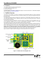
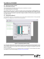
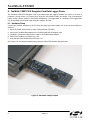
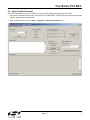
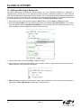
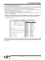
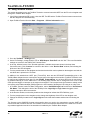
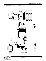
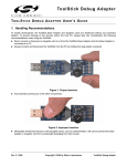
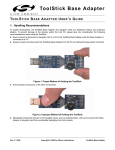
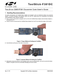
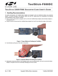
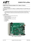
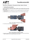
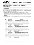
To o l Sti c k - F 9 1 2 D C TO O L S T I C K C 8 0 5 1 F 9 1 2 D A U G H T E R C A R D U S E R ’ S G U I DE 1. Handling Recommendations To enable development, the ToolStick Base Adapter and daughter cards are distributed without any protective plastics. To prevent damage to the devices and/or the host PC, please take into consideration the following recommendations when using the ToolStick: Never connect or disconnect a daughter card to or from the ToolStick Base Adapter while the Base Adapter is connected to a PC. Always connect and disconnect the ToolStick Base Adapter from the PC by holding the edges of the boards. Figure 1. Proper Method of Holding the ToolStick Avoid directly touching any of the other components. Figure 2. Improper Method of Holding the ToolStick Manipulate mechanical devices on the daughter cards, such as potentiometers, with care to prevent the Base Adapter or daughter card from accidentally dislodging from their sockets. Rev. 0.1 7/09 Copyright © 2009 by Silicon Laboratories ToolStick-C8051F912DC ToolStic k- F 912DC 2. Contents The ToolStick-F912DC kit contains the following items: ToolStick C8051F912 Daughter Card One extra A76 battery A ToolStick daughter card requires a ToolStick Base Adapter to communicate with the PC. ToolStick Base Adapters can be purchased at www.silabs.com/toolstick. 3. ToolStick Overview The purpose of the ToolStick is to provide a development and demonstration platform for Silicon Laboratories microcontrollers and to demonstrate the Silicon Laboratories software tools, including the Integrated Development Environment (IDE). The ToolStick development platform consists of two components: the ToolStick Base Adapter and a daughter card. The ToolStick Base Adapter provides a USB debug interface and data communications path between a Windows PC and a target microcontroller. The target microcontroller and application circuitry are located on the daughter card. Some daughter cards, such as the C8051F912 Daughter Card, are used as general-purpose development platforms for the target microcontrollers and some are used to demonstrate a specific feature or application. The C8051F912 Daughter Card includes a pair of GPIO controlled LEDs, a potentiometer, a switch connected to a GPIO, a capacitive touch sense switch, and a small prototyping area which provides access to all of the pins of the device. This prototyping area can be used to connect additional hardware to the microcontroller and use the daughter card as a development platform. The C8051F912 Daughter Card also includes an A76 1.5 V alkaline battery which can be used to power the board when not connected to the Toolstick Base Adapter. The C8051F912 will continue to operate from the single “button cell” battery until the supply voltage drops below 0.9 V. Figure 3 shows the ToolStick C8051F912 Daughter Card and identifies the various components. P1.6 P1.5 Red LED Yellow LED Full Pin Access ToolStick Power Available Red LED Power Source Indicator Yellow LED Power Source Selector Switch C8051F912 P0.3 Capacitive P0.2 Push Touch Sense Button Switch (S2) Switch P0.6 Potentiometer Figure 3. ToolStick C8051F912 Daughter Card 2 Rev. 0.1 ToolStick-F912DC 4. Getting Started The necessary software to download, debug and communicate with the target microcontroller must be downloaded from www.silabs.com/toolstick. The following software is necessary to build a project, download code to, and communicate with the target microcontroller: Silicon Laboratories Integrated Development Environment (IDE) Keil Demonstration Tools ToolStick Terminal application The Keil Demo Tools include a compiler, assembler, and linker. The limitation of the demo version is the resulting object code is limited to 2 kBytes. ToolStick Terminal communicates with the target microcontroller's UART through the ToolStick Base Adapter. It can also read/write the two GPIO pins available on the ToolStick Base Adapter. Other useful software that is provided on the Silicon Labs Downloads (www.silabs.com/mcudownloads) website includes the following: Configuration Wizard 2 Keil µVision2 and µVision3 Drivers All of the above software is described in more detail in Section “5. Software Overview”. The software described above is provided in several download packages. The ToolStick Download package includes example code, documentation including user’s guides and data sheets, and the ToolStick Terminal application. The IDE, Keil Demonstration Tools, Configuration Wizard 2, and the Keil µVision Drivers are available as separate downloads. After downloading and installing these packages, see the following sections for information regarding the software and running one of the demo applications. 5. Software Overview 5.1. Silicon Laboratories IDE The Silicon Laboratories IDE integrates a source-code editor, source-level debugger, and an in-system Flash programmer. See Section “7. ToolStick C8051F912 Daughter Card Features Demo” for detailed information on how to use the IDE. The Keil Demonstration Toolset includes a compiler, linker, and assembler and easily integrates into the IDE. The use of third-party compilers and assemblers is also supported. 5.1.1. IDE System Requirements The Silicon Laboratories IDE requirements: Pentium-class host PC running Microsoft Windows 2000 or Windows XP. One available USB port. 64 MB RAM and 40 MB free HD space recommended. 5.1.2. 3rd Party Toolsets The Silicon Laboratories IDE has native support for many 8051 compilers. The full list of natively supported tools is as follows: Keil IAR Raisonance Tasking Hi-Tech SDCC The demo applications for the C8051F912 Daughter Card are written for the Keil and SDCC toolsets. Rev. 0.1 3 ToolStic k- F 912DC 5.2. Keil Demonstration Toolset 5.2.1. Keil Assembler and Linker The Keil demonstration toolset assembler and linker place no restrictions on code size. 5.2.2. Keil Demonstration C51 C Compiler The evaluation version of the C51 compiler is the same as the full version with the following limitations: (1) Maximum 4 kB code generation, (2) There is no floating point library included. When initially installed, the C51 compiler is limited to a code size of 2 kB, and programs start at code address 0x0800. Refer to “AN104: Integrating Keil Tools into the Silicon Labs IDE" for instructions to change the limitation to 4 kB and have the programs start at code address 0x0000. 5.3. Configuration Wizard 2 The Configuration Wizard 2 is a code generation tool for all of the Silicon Laboratories devices. Code is generated through the use of dialog boxes for each of the device's peripherals. Figure 4. Configuration Wizard 2 Utility The Configuration Wizard 2 utility helps accelerate development by automatically generating initialization source code to configure and enable the on-chip resources needed by most design projects. In just a few steps, the wizard creates complete startup code for a specific Silicon Laboratories MCU. The program is configurable to provide the output in C or assembly. For more information, please refer to the Configuration Wizard 2 documentation. The documentation and software are available from the Downloads webpage (www.silabs.com/mcudownloads). 4 Rev. 0.1 ToolStick-F912DC 5.4. Keil µVision2 and µVision3 Silicon Laboratories Drivers As an alternative to the Silicon Laboratories IDE, the uVision debug driver allows the Keil µVision2 and µVision3 IDEs to communicate with Silicon Laboratories on-chip debug logic. In-system Flash memory programming integrated into the driver allows for rapidly updating target code. The µVision2 and µVision3 IDEs can be used to start and stop program execution, set breakpoints, check variables, inspect and modify memory contents, and single-step through programs running on the actual target hardware. For more information, please refer to the µVision driver documentation. The documentation and software are available from the Downloads webpage (www.silabs.com/mcudownloads). 5.5. ToolStick Terminal The ToolStick Terminal program provides the standard terminal interface to the target microcontroller's UART. However, instead of requiring the usual RS-232 and COM port connection, ToolStick Terminal uses the USB interface of the ToolStick Base Adapter to provide the same functionality. In addition to the standard terminal functions (send file, receive file, change baud rate), two GPIO pins on the target microcontroller can be controlled using the Terminal for either RTS/CTS handshaking or software-configurable purposes (see the demo software for an example). See Section "7.8. Using ToolStick Terminal‚" on page 16 for more information. The software is available on the ToolStick webpage (www.silabs.com/toolstick). Rev. 0.1 5 ToolStic k- F 912DC 6. ToolStick C8051F912 Daughter Card Data Logger Demo The ToolStick C8051F912 Daughter Card is pre-loaded with data logging firmware and turned on at time of production. During transit, it is powered by a single-cell A76 alkaline battery and keeps a log of temperature, battery voltage, and the number of hours since manufacture. The logged data, or a summary of the logged data, may be extracted from the data logger using the ToolStick Terminal. 6.1. Hardware Setup Connect the ToolStick hardware to the PC using the steps below while taking note of the recommendations in Section 1: 1. Set the S1 Power Select Switch to select ToolStick Power (TS PWR). 2. Connect the ToolStick Base Adapter to the ToolStick C8051F912 Daughter Card. 3. If available, connect the USB extension cable to the ToolStick Base Adapter. 4. Connect the ToolStick to a USB port on a PC. 5. Verify that the Yellow Power Select LED (D2) is on. See Figure 5 for an example hardware setup using the C8051F330 ToolStick Daughter Card. Figure 5. Hardware Setup Example 6 Rev. 0.1 ToolStick-F912DC 6.2. Using ToolStick Terminal This section describes how to use ToolStick Terminal to view the logged data and other information. 1. If the Silicon Laboratories IDE is open, close the IDE. The IDE and the ToolStick Terminal cannot communicate with the daughter card simultaneously. 2. Open ToolStick Terminal from the Start Programs Silicon Laboratories menu. Rev. 0.1 7 ToolStic k- F 912DC 3. Click on the Connect button. A Log Summary should appear as shown below. 8 Rev. 0.1 ToolStick-F912DC 4. Press the S2 switch on the C8051F912 Daughter Card. This will place the system in Interactive mode. In this mode, the ToolStick Terminal is continuously refreshed with information about the number of seconds remaining until the next Log entry, the current potentiometer ratio (%), the oscillation period of the Capacitive Touch Sense Switch (SYSCLKs), and the current temperature (degrees C). Press the S2 switch again to return to the log summary. 5. Type the letter “P” into the Transfer Data text entry field and press the “Send Data” button to print the entire log to the ToolStick Terminal. Note: This step may take a few minutes depending on the log size. 6.3. Data Logger Modes and Indicator LEDs The data logger has three modes of operation shown in Table 1: Table 1. Data Logger Modes Mode Power Source Reset Source Blinking Indicator LED(s) Logging Only Battery POR or other Yellow Only Logging + UART Battery /RST Pin Red Only ToolStick Base Adapter Don’t Care Red and Yellow Interactive The Logging Only mode is the lowest power mode and is the mode in which the data logger spends most of its operating life. The primary goal of this mode is to prolong battery life and keep the data log up to date. The system enters this mode when it is powered from the battery and the last reset was a power on reset or other reset not caused by the reset pin. In this mode, the Yellow LED will blink when the S2 switch is pressed to indicate that the system is in its lowest power mode. The Logging + UART mode is entered when powered from the battery and a pin reset occurs. A pin reset is generated on the C8051F912 Daughter Card when the ToolStick Terminal is connected. In this mode, the device prints a log summary to the screen and blinks the Red LED when the S2 switch is pressed. This mode preserves battery life, but it requires the MCU to stay in active mode while transmitting information over UART. When the power source is set to ToolStick Power, the data logger will enter Interactive Mode. Since the MCU is powered from the ToolStick Base Adapter, it runs at full speed without entering a low power mode. It constantly monitors the potentiometer ratio, the capacitive touch sense switch oscillation period, and the current temperature. Since the battery is disconnected when being powered from the ToolStick Base Adapter, the MCU cannot measure the battery voltage. When S2 is pressed, the system toggles between displaying a log summary and interactive content in addition to blinking both the Yellow and Red LEDs. Rev. 0.1 9 ToolStic k- F 912DC 7. ToolStick C8051F912 Daughter Card Features Demo The ToolStick kit includes a few simple code examples. The example described in this section is titled F912DC_FeaturesDemo. The purpose of this example is to guide a new user through the features and capabilities of the IDE and demonstrate the microcontroller’s on-chip debug capabilities. The F912DC_FeaturesDemo example code uses the potentiometer on the daughter card to vary the blinking rate of the LED. The first part of this demo shows how to use the IDE to connect and download the firmware, view and modify registers, use watch windows, use breakpoints, and single step through code. The second part of the demo shows how to use ToolStick Terminal to receive UART data from the daughter card and how to use the GPIO pins. 7.1. Hardware Setup Connect the ToolStick hardware to the PC using the steps below while taking note of the recommendations in Section 1: 1. Connect the ToolStick Base Adapter to the ToolStick C8051F912 Daughter Card. 2. If available, connect the USB extension cable to the ToolStick Base Adapter. 3. Connect the ToolStick to a USB port on a PC. See Figure 6 for an example hardware setup using the C8051F330 ToolStick Daughter Card. Figure 6. Hardware Setup Example 10 Rev. 0.1 ToolStick-F912DC 7.2. Connecting to the Device and Downloading Firmware This section describes how to open the IDE, open and build a project, connect to a device and download the firmware. 1. Open the Silicon Laboratories IDE from the Start Programs Silicon Laboratories menu. 2. In the IDE, go to Project Open Project. 3. Browse to the default installation location C:\SiLabs\MCU\ToolStick\F912DC\Firmware\. 4. Select F912DC_FeaturesDemo.wsp and click OK. 5. In the IDE, select Project Rebuild Project. 6. Go to Options Connection Options. 7. Select “USB Debug Adapter” for the Serial Adapter and “C2” for the Debug Interface, and then click “OK”. 8. Go to Debug Connect. 9. Download the code using the download button on the menu bar or use alt-D. Once these steps are completed, the firmware is built into an object file (step 5) and downloaded to the device (step 9). The device is now ready to begin executing code. If all of these steps were followed successfully, the “Go” option is enabled in the Debug menu. A green circle icon in the IDE toolbar also indicates that the device is ready to run. If one of the steps leads to an error, make sure that the ToolStick is properly inserted in a USB port and start again with step 6. 7.3. Running and Stopping Code Execution Once the IDE is connected to the device and the firmware is loaded, the IDE can start and stop the code execution. The following steps can be performed using the buttons on the toolbar or using the options in the Debug menu. 1. To start code execution, click the green “Go” button on the toolbar or use the Debug Go menu option. The green LED on the daughter card will start to flash. The debug commands in the IDE (single-step, multiple-step, set breakpoint, and others) are disabled when the device is running. While the firmware is running, the potentiometer on the daughter card can be turned to alter the blinking speed of the LED. The button labeled P2.4 can also be pressed to toggle the ADC on and off. When the ADC is off, the blink rate or brightness of the LED will not change. 2. To stop code execution, click the red “Stop” button on the toolbar or use the Debug Stop menu option. The device will halt code execution and all of the registers and pins on the device will hold their state. All debug windows and watch windows are refreshed when the device is stopped. If any of the values in these windows have changed since the last time the device was halted, the new value is shown in red text instead of black text. Rev. 0.1 11 ToolStic k- F 912DC 7.4. Viewing and Modifying Registers All registers on the device can be viewed and modified when the device is in a halted state. The registers are grouped together according to which peripheral or part of hardware they belong. As an example, this guide shows how to open the ADC0 Debug Window and disable the ADC0 directly from the IDE. 1. Open the ADC0 Debug Window from the View Debug Windows SFR’s ADC0 menu option. The ADC0 Debug Window appears on the right-hand side of the IDE. In this window, the ADC0CN register is shown. This register is used to enable and configure the on-chip ADC. When the firmware is running, the ADC0CN register reads as 0x82 indicating that the ADC is running. 2. In the debug window, change the value of ADC0CN from 0x82 to 0x02. This value turns off the ADC on the target microcontroller. 3. To write this new value to the device, select Refresh from the Debug Menu or click the Refresh button in the toolbar. 4. Click “Go” to resume running the device with the new ADC0CN value. 5. Turn the potentiometer on the daughter card and notice that it has no effect on the blinking rate of the LED. 6. Re-enable the ADC by writing 0x82 to the ADC0CN and clicking the Refresh button. 12 Rev. 0.1 ToolStick-F912DC Changing the values of registers does not require recompiling the code and redownloading the firmware. At any time, the device can be halted and the values of the registers can be changed. After selecting “Go”, the firmware will continue execution using the new values. This capability greatly speeds up the debugging process. See the data sheet for the C8051F91x-C8051F90x device family for the definitions and usage for all registers. The debug windows for other sets of registers are found in the View Debug Windows SFR’s menu. 7.5. Enabling and Using Watch Windows The Debug Windows in the View menu are used to view and modify hardware registers. To view and modify variables in code, the IDE provides Watch Windows. Just as with register debug windows, variables in the watch windows are updated each time the device is halted. This section of the User’s Guide explains how to add a variable to the watch window and modify the variable. In the F912DC_FeaturesDemo example code, the variable Num_LED_Flashes is a counter that stores the number of times the LED blinks. 1. If the device is running, stop execution using the “Stop” button or use the Debug Stop menu option. 2. In the File View on the left-hand side of the IDE, double-click on F912DC_FeaturesDemo.c to open the source file. 3. Scroll to the Timer3_ISR function (line 684) and right-click on the variable “Num_LED_Flashes”. In the context menu that appears, select “Add Num_LED_Flashes to Watch” and then choose “Default.” On the right-hand portion of the IDE, the watch window appears and the variable is added. The current value of the variable is shown to the right of the name. 4. Start and stop the device a few times. See that the value of the Num_LED_Flashes is incremented each time the LED blinks. 5. When the device is halted, click on the value field in the watch window and change the value to 0. Then click the Refresh button or select Debug Refresh to write the new value to the device. 6. Start and stop the device a few times to watch the variable increment starting at 0. Changing the values of variables does not require recompiling the code and redownloading the firmware. At any time, the device can be halted and the values of the variables can be changed. The firmware will continue execution using the new values. Rev. 0.1 13 ToolStic k- F 912DC 7.6. Setting and Running to Breakpoints The Silicon Laboratories microcontroller devices support up to four hardware breakpoints. A breakpoint is associated with a specific line of code. When the processor reaches a hardware breakpoint, the code execution stops, and the IDE refreshes all debug and watch windows. The on-chip debug hardware allows for breakpoints to be placed on any line of executable code, including code in Interrupt Service Routines. This section provides steps to set a breakpoint on the line of source code that increments the Num_LED_Flashes variable. 1. If the device is running, stop execution using the “Stop” button or use the Debug Stop menu option. 2. Scroll to the Timer3_ISR function (line 684) and right-click on the variable “Num_LED_Flashes”. In the context menu that appears, select “Insert/Remove Breakpoint.” On the left side of the line in the editor window, a red circle is added to indicate a breakpoint is placed on the source line. 3. Click the “Go” button or select the Debug Go menu option. 4. After a short time, the IDE will show that the device is halted. A blue line will be placed in the editor window to indicate where the code execution has stopped. 5. Start and stop the processor a few more times. Notice that the LED blinks once for every time the processor is started and the Num_LED_Flashes variable also increments by one. 14 Rev. 0.1 ToolStick-F912DC 7.7. Single-Stepping Through Firmware The IDE supports the ability to single-step through firmware one assembly instruction at a time. The IDE reads the Flash from the device, converts the instructions to assembly and displays them in a disassembly window. The following steps show how to open the disassembly window and single step through firmware. 1. If there is already not a breakpoint set on line of code that increments the Num_LED_Flashes variable, set the breakpoint using the steps described in Section 7.6. 2. Start the processor using the “Go” button and wait till it stops on the breakpoint. 3. Select View Debug Windows Disassembly. The disassembly window will appear on the right-hand side of the IDE, if it is not already open. 4. To execute one assembly instruction at a time, click the “Step” button on the toolbar or select the Debug Step menu option. The highlighted line in the disassembly window indicates the next instruction to be executed. The blue line marker in the editor window will stay on the same .C source line until all of the assembly instructions are completed. The disassembly window has three columns. The left column is the address of the instruction in Flash. The middle column is the instruction in hex. The right column is the disassembled instruction. The Disassembly debug window and the capability to single-step through firmware allows a developer to see exactly what instructions are executed and their output. Rev. 0.1 15 ToolStic k- F 912DC 7.8. Using ToolStick Terminal This section describes how to use ToolStick Terminal to communicate with UART from the PC to the daughter card through the ToolStick Base Adapter. 1. If the Silicon Laboratories IDE is open, close the IDE. The IDE and the ToolStick Terminal cannot communicate with the daughter card simultaneously. 2. Open ToolStick Terminal from the Start Programs Silicon Laboratories menu. 3. Go to the ToolStick Settings menu. 4. Under “Pin Settings”, change GPIO0 / RTS to “GPIO Output - Push Pull” and click “OK.” The rest of the default settings are correct for the C8051F912 Features Demo. 5. In the top, left-hand corner of the Terminal application, available devices are shown in the drop-down Connection menu. Click “Connect” to connect to the device. In the “Receive Data” window, text indicating the blink rate of the LED will appear. 6. Turn the potentiometer on the daughter card and see that the blink rate is updated on the daughter card and the new blink rate is printed to the Terminal. In addition to the standard two UART pins (TX and RX), there are two GPIO/UART handshaking pins on the ToolStick Base Adapter that are connected to two port pins on the target microcontroller. ToolStick Terminal is used to configure and read/write these pins. For the F912DC_FeaturesDemo, one of these GPIO pins is connected to an external interrupt pin on the C8051F912. The following steps describe how to change the level of one of the GPIO pins and trigger an interrupt on the target microcontroller. The interrupt forces the firmware to switch modes and send a pulse-width modulated (PWM) signal to the LED instead of blinking the LED using an on-chip Timer. 1. In ToolStick Terminal, under Pin State Configuration, select “Set GPIO0 Logic Low” and click on “Set Selected Pin States.” This changes the level of the GPIO0 pin from Logic High to Logic Low and triggers a levelsensitive interrupt on the microcontroller. 2. In the Receive window, see that the printed text has changed to indicate the LED PWM duty cycle. 3. Turn the potentiometer on the daughter card to change the brightness of the LED on the daughter card. 4. Change the GPIO0 pin state back to Logic High and notice that the firmware switches back to blinking the LED. The firmware on the C8051F912 target microcontroller does not need to be customized to use the UART and communicate with ToolStick Terminal. The firmware on the microcontroller should write to the UART as it would in any standard application and all of the translation is handled by the ToolStick Base Adapter. 16 Rev. 0.1 ToolStick-F912DC 8. Additional Demo Examples In addition to the F912DC_FeaturesDemo example firmware, the ToolStick download package also includes demo projects named F912DC_CapTouchSense_Tune and F912DC_CapTouchSense_Switch. The instructions for running these demos can be found at the top of the source file. The project and source files for these C:\SiLabs\MCU\ToolStick\F912DC\Firmware\ folder. demos can be found by default in the 9. Using the C8051F912 Daughter Card as a Development Platform The prototyping area on the ToolStick C8051F912 Daughter Card makes it easy to interface to external hardware. All of the digital I/O pins are available so it possible to create a complete system. 9.1. C8051F912 Pin Connections It is important to note that if external hardware is being added, some of the existing components on the board can interfere with the signaling. The following is a list of port pins on the C8051F912 that are connected to other components: P0.2—This pin is connected to the P0.2 switch. The switch and R10 can be safely removed from the daughter card if they are not needed. P0.3—This pin is connected to a capacitive touch sense switch. The 0 resistor R15 can be safely removed from the daughter card if the capacitive touch sense switch is not needed. P0.4, P0.5—These pins are connected directly to the ToolStick Base Adapter for UART communication. P0.6—This pin is connected to the output of the potentiometer. The 0 resistor R11 can be removed to disconnect the potentiometer from the pin. P1.0, P1.1—These pins are connected directly to the ToolStick Base Adapter’s GPIO pins. By default, these GPIO pins on the Base Adapter are high-impedance pins so they will not affect any signaling. Configuring these pins on the Base Adapter to output pin or handshaking pins could affect signaling. P1.3—This pin is connected to the power source detect signal. P1.4—This pin is connected to the potentiometer enable signal. This allows the potentiometer to be disabled by software when not in use. The 0 resistor R11 can be safely removed from the daughter card to disconnect the potentiometer enable from the pin. P1.5—This pin is connected to the cathode (-) of the red LED on the daughter card. The LED or R4 resistor can be removed to disconnect the LED from the pin. P1.6—This pin is connected to the cathode (-) of the yellow LED on the daughter card. The LED or R5 resistor can be removed to disconnect the LED from the pin. See the daughter card schematic in Section 11 for more information. 9.2. VREF Capacitor On the C8051F912 devices, if VREF is generated using the High-Speed Internal Reference, no output capacitor is required. If using the on-chip Precision Voltage Reference, it is highly recommended to place a capacitor on the VREF output pin. On the ToolStick C8051F912 Daughter Card, there are pads on the board (C5) to populate a 0603 surface mount capacitor. There are also pads on the board (R14) to facilitate shorting P0.1 to the ground plane for use as an analog ground reference (AGND). The firmware examples for the daughter card use the HighSpeed Internal Reference as VREF and the GND pin as a ground reference, so no external capacitor on P0.0 is necessary for proper operation. Also, P0.1 may be used for general purpose I/O. 9.3. C2 Pin Sharing On the C8051F912, the debug pins, C2CK, and C2D, are shared with the pins /RST and P2.7 respectively. The daughter card includes the resistors necessary to enable pin sharing which allow the /RST and P2.7 pins to be used normally while simultaneously debugging the device. See Application Note “AN124: Pin Sharing Techniques for the C2 Interface” at www.silabs.com for more information regarding pin sharing. Rev. 0.1 17 ToolStic k- F 912DC 10. Information Locations Example source code is installed by default in the “C:\SiLabs\MCU\ToolStick\F912DC\Firmware” directory during the ToolStick installation. Documentation for the ToolStick kit, including this User’s Guide, can be found by default in the C:\SiLabs\MCU\ToolStick\Documentation and the C:\SiLabs\MCU\ToolStick\F912DC\Documentation directories. The installer for the ToolStick software is available at www.silabs.com/toolstick. 18 Rev. 0.1 PWR R1 4k7 VBUS_OUT Rev. 0.1 TCK_C2D 6 TDO_C2CKPS 8 GND C2 X7R 1.0UF VDD NEG POS RF2 RUBBER FOOT 2 1 FI1 FIDUCIAL TP4 R2 0.0 TP5 1K 680nH L1 P1.3 SUSPEND C3 X7R 4.7UF D2 1.8V YELLOW TP25 I measure R16 R3 1.2K DC+ VDD Power Source P0.4 P1.1 C2D DC+ FI2 FIDUCIAL DC+ 6 3 4 5 S1 2 1 VPPCTL(OUT) 14 TSTERMINAL_RX 10 GPIO1_CTS 12 BAT2 NEG_BATTERY_CONTACT GND RF1 RUBBER FOOT D1 1.8V RED 3 2 1 1.5V 11.6mm POS NEG POS Button Cell BAT1 13 SUSPEND(OUT) 9 TSTERMINAL_TX 11 GPIO0_RTS SUSPEND 5 TDI_C2CK 7 TDO_C2DPS P0.5 P1.0 2 4 TOP SIDE J1 EDGE-MEC1-108-02-F-D-EM2 1 GND VDD(3.3V) 3 VBUS(5V) VIO(IN) C2CK P2.7 GND VBUS_OUT CARD EDGE CONNECTOR BOTTOM SIDE 3 VBAT DCEN GND/DC- VDD/DC+ 2 GND 25 DAP 5 4 C4 X7R 1.0UF 1 DC+ P0.0/VREF 8 9 16 15 14 13 12 11 10 23 22 21 20 19 18 17 24 6 RST/C2CK 7 P2.7/C2D XTAL4 XTAL3 P1.0 P1.1 P1.2 P1.3 P1.4 P1.5 P1.6 P0.1/AGND P0.2/XTAL1 P0.3/XTAL2 P0.4/TX P0.5/RX P0.6/CNVSTR P0.7/IREF0 U1 C8051F912 C5 X7R P0.1 C2CK C2D TP26 TP1 NO POP R14 Y1 32.768KHZ P1.0 P1.1 P1.2 P1.3 P1.4 P1.5 P1.6 P0.4 P0.5 P0.6 P0.2 NO POP TP3 DC+ R13 NO POP NO POP C6 R12 NO POP DC+ NO POP C7 P1.5 P1.6 P0.3 TP13 TP12 TP11 TP10 TP9 TP8 TP7 TP6 P0.7 P0.3 P0.2 P1.4 P0.6 C2D C2CK DRAWN BY: PART NUMBER: TITLE: P0.7 (IREF0/GPIO) TP22 10K R8 D4 1.8V RED P2.7 (C2D/GPIO) P1.6 (Orange LED) P1.5 (Red LED) P1.4 (Potentiometer Bias) P1.3 (Power Source) P1.2 (GPIO) P1.1 (GPIO1_CTS/GPIO) P1.0 (GPIO0_RTS/GPIO) P1/P2 D3 R5 1.2K SILICON LABS TP21 TP20 TP19 TP18 TP17 TP16 TP15 TP14 GND C2CK C2D R4 1.2K DC+ 1.8V YELLOW DC+ TP24 TP23 ENGINEER: - SA-TS077PCB-000 TOOLSTICK F912 DC AnGa R P0.6 (CNVSTR/Potentiometer) P0.5 (RX) P0.4 (TX) P0.3 (XTAL2/TouchSense/GPIO) S3 S2 C2D P2.7 C2CK DEBUG CIRCUIT P0.2 (XTAL1/Switch/GPIO) P0.1 (AGND/GPIO) P0.0 (VREF/GPIO) P0 TOUCH SENSE SWITCH R15 0.0 R10 1K R11 0.0 R9 1K 1K R7 R6 1K DC+ ToolStick-F912DC 11. C8051F912 Daughter Card Schematic 19 P0.0 ToolStic k- F 912DC CONTACT INFORMATION Silicon Laboratories Inc. 400 West Cesar Chavez Austin, TX 78701 Tel: 1+(512) 416-8500 Fax: 1+(512) 416-9669 Toll Free: 1+(877) 444-3032 Please visit the Silicon Labs Technical Support web page: https://www.silabs.com/support/pages/contacttechnicalsupport.aspx and register to submit a technical support request. The information in this document is believed to be accurate in all respects at the time of publication but is subject to change without notice. Silicon Laboratories assumes no responsibility for errors and omissions, and disclaims responsibility for any consequences resulting from the use of information included herein. Additionally, Silicon Laboratories assumes no responsibility for the functioning of undescribed features or parameters. Silicon Laboratories reserves the right to make changes without further notice. Silicon Laboratories makes no warranty, representation or guarantee regarding the suitability of its products for any particular purpose, nor does Silicon Laboratories assume any liability arising out of the application or use of any product or circuit, and specifically disclaims any and all liability, including without limitation consequential or incidental damages. Silicon Laboratories products are not designed, intended, or authorized for use in applications intended to support or sustain life, or for any other application in which the failure of the Silicon Laboratories product could create a situation where personal injury or death may occur. Should Buyer purchase or use Silicon Laboratories products for any such unintended or unauthorized application, Buyer shall indemnify and hold Silicon Laboratories harmless against all claims and damages. Silicon Laboratories and Silicon Labs are trademarks of Silicon Laboratories Inc. Other products or brandnames mentioned herein are trademarks or registered trademarks of their respective holders. 20 Rev. 0.1