1
Chapter 6: Functional Description—High-Performance Controller II
Example Top-Level File
6–21
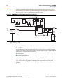
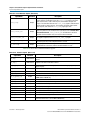
Both the memory models display similar behaviors and have the same calibration
time.
1
The memory model, <variation name>_test_component.v/vhd, used in SOPC Builder
designs, is actually a variation of the full-array memory model. To ensure your
simulation works in SOPC Builder, use memory model with less than 512-Mbit
capacity.
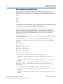
Example Driver
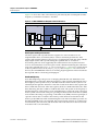
The example driver is a self-checking test pattern generator for the memory interface.
It uses a state machine to write and read from the memory to verify that the interface
is operating correctly.
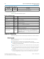
The example driver performs the following tests and loops back the tests indefinitely:
■
Sequential addressing writes and reads
The state machine writes pseudo-random data generated by a linear feedback shift
register (LFSR) to a set of incrementing row, bank, and column addresses. The
state machine then resets the LFSR, reads back the same set of addresses, and
compares the data it receives against the expected data. You can adjust the length
and pattern of the bursts that are written by changing the MAX_ROW, MAX_BANK, and
MAX_COL constants in the example driver source code, and the entire memory space
can be tested by adjusting these values. You can skip this test by setting the
test_seq_addr_on signal to logic zero.
■
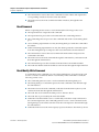
Incomplete write operation
The state machine issues a series of write requests that are less than the maximum
burst size supported by your controller variation. The addresses are then read
back to ensure that the controller has issued the correct signals to the memory. This
test is only applicable in full-rate mode, when the local burst size is two. You can
skip this test by setting the test_incomplete_writes_on signal to logic zero.
■
Byte enable/data mask pin operation
The state machine issues two sets of write commands, the first of which clears a
range of addresses. The second set of write commands has only one byte enable bit
asserted. The state machine then issues a read request to the same addresses and
the data is verified. This test checks if the data mask pins are operating correctly.
You can skip this test by setting the test_dm_pin_on signal to logic zero.
■
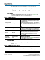
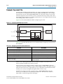
Address pin operation
The example driver generates a series of write and read requests starting with an
all-zeros pattern, a walking-one pattern, a walking-zero pattern, and ending with
an all-zeros pattern. This test checks to make sure that all the individual address
bits are operating correctly. You can skip this test by setting the test_addr_pin_on
signal to logic zero.
June 2011
Altera Corporation
External Memory Interface Handbook Volume 3
Section II. DDR3 SDRAM Controller with ALTMEMPHY IP User Guide