1
SOPC Builder User Guide
SOPC Builder
User Guide
101 Innovation Drive
San Jose, CA 95134
www.altera.com
UG-01096-1.0
Subscribe
© 2010 Altera Corporation. All rights reserved. ALTERA, ARRIA, CYCLONE, HARDCOPY, MAX, MEGACORE, NIOS, QUARTUS and STRATIX are Reg. U.S. Pat.
& Tm. Off. and/or trademarks of Altera Corporation in the U.S. and other countries. All other trademarks and service marks are the property of their respective
holders as described at www.altera.com/common/legal.html. Altera warrants performance of its semiconductor products to current specifications in accordance
with Altera’s standard warranty, but reserves the right to make changes to any products and services at any time without notice. Altera assumes no responsibility or
liability arising out of the application or use of any information, product, or service described herein except as expressly agreed to in writing by Altera. Altera
customers are advised to obtain the latest version of device specifications before relying on any published information and before placing orders for products or
services.
SOPC Builder User Guide
December 2010 Altera Corporation
Contents
Chapter 1. Introduction to SOPC Builder
Architecture of SOPC Builder Systems . . . . . . . . . . . . . . . . . . . . . . . . . . . . . . . . . . . . . . . . . . . . . . . . . . . . . 1–1
SOPC Builder Modules . . . . . . . . . . . . . . . . . . . . . . . . . . . . . . . . . . . . . . . . . . . . . . . . . . . . . . . . . . . . . . . . 1–2
Functions of SOPC Builder . . . . . . . . . . . . . . . . . . . . . . . . . . . . . . . . . . . . . . . . . . . . . . . . . . . . . . . . . . . . . . . 1–5
Defining and Generating the System Hardware . . . . . . . . . . . . . . . . . . . . . . . . . . . . . . . . . . . . . . . . . . . 1–5
Creating a Memory Map for Software Development . . . . . . . . . . . . . . . . . . . . . . . . . . . . . . . . . . . . . . . 1–6
Creating a Simulation Model and Test Bench . . . . . . . . . . . . . . . . . . . . . . . . . . . . . . . . . . . . . . . . . . . . . 1–6
SOPC Builder Design Flow . . . . . . . . . . . . . . . . . . . . . . . . . . . . . . . . . . . . . . . . . . . . . . . . . . . . . . . . . . . . . . . 1–6
Visualization of SOPC Builder Systems . . . . . . . . . . . . . . . . . . . . . . . . . . . . . . . . . . . . . . . . . . . . . . . . . . . . . 1–8
Operating System Support . . . . . . . . . . . . . . . . . . . . . . . . . . . . . . . . . . . . . . . . . . . . . . . . . . . . . . . . . . . . . . . . 1–8
Talkback Support . . . . . . . . . . . . . . . . . . . . . . . . . . . . . . . . . . . . . . . . . . . . . . . . . . . . . . . . . . . . . . . . . . . . . . . 1–8
Chapter 2. System Interconnect Fabric for Memory-Mapped Interfaces
High-Level Description . . . . . . . . . . . . . . . . . . . . . . . . . . . . . . . . . . . . . . . . . . . . . . . . . . . . . . . . . . . . . . . . . . 2–1
Fundamentals of Implementation . . . . . . . . . . . . . . . . . . . . . . . . . . . . . . . . . . . . . . . . . . . . . . . . . . . . . . . . . . 2–3
Functions of System Interconnect Fabric . . . . . . . . . . . . . . . . . . . . . . . . . . . . . . . . . . . . . . . . . . . . . . . . . . . . 2–3
Address Decoding . . . . . . . . . . . . . . . . . . . . . . . . . . . . . . . . . . . . . . . . . . . . . . . . . . . . . . . . . . . . . . . . . . . . . . . 2–3
Datapath Multiplexing . . . . . . . . . . . . . . . . . . . . . . . . . . . . . . . . . . . . . . . . . . . . . . . . . . . . . . . . . . . . . . . . . . . 2–4
Wait State Insertion . . . . . . . . . . . . . . . . . . . . . . . . . . . . . . . . . . . . . . . . . . . . . . . . . . . . . . . . . . . . . . . . . . . . . . 2–5
Pipelined Read Transfers . . . . . . . . . . . . . . . . . . . . . . . . . . . . . . . . . . . . . . . . . . . . . . . . . . . . . . . . . . . . . . . . . 2–6
Dynamic Bus Sizing and Native Address Alignment . . . . . . . . . . . . . . . . . . . . . . . . . . . . . . . . . . . . . . . . . 2–6
Dynamic Bus Sizing . . . . . . . . . . . . . . . . . . . . . . . . . . . . . . . . . . . . . . . . . . . . . . . . . . . . . . . . . . . . . . . . . . . 2–7
Native Address Alignment . . . . . . . . . . . . . . . . . . . . . . . . . . . . . . . . . . . . . . . . . . . . . . . . . . . . . . . . . . . . . 2–8
Arbitration for Multimaster Systems . . . . . . . . . . . . . . . . . . . . . . . . . . . . . . . . . . . . . . . . . . . . . . . . . . . . . . . 2–9
Traditional Shared Bus Architectures . . . . . . . . . . . . . . . . . . . . . . . . . . . . . . . . . . . . . . . . . . . . . . . . . . . . 2–9
Slave-Side Arbitration . . . . . . . . . . . . . . . . . . . . . . . . . . . . . . . . . . . . . . . . . . . . . . . . . . . . . . . . . . . . . . . . 2–10
Arbiter Details . . . . . . . . . . . . . . . . . . . . . . . . . . . . . . . . . . . . . . . . . . . . . . . . . . . . . . . . . . . . . . . . . . . . . . . 2–11
Arbitration Rules . . . . . . . . . . . . . . . . . . . . . . . . . . . . . . . . . . . . . . . . . . . . . . . . . . . . . . . . . . . . . . . . . . . . 2–12
Burst Adapters . . . . . . . . . . . . . . . . . . . . . . . . . . . . . . . . . . . . . . . . . . . . . . . . . . . . . . . . . . . . . . . . . . . . . . . . . 2–14
Interrupts . . . . . . . . . . . . . . . . . . . . . . . . . . . . . . . . . . . . . . . . . . . . . . . . . . . . . . . . . . . . . . . . . . . . . . . . . . . . . 2–15
Individual Requests IRQ Scheme . . . . . . . . . . . . . . . . . . . . . . . . . . . . . . . . . . . . . . . . . . . . . . . . . . . . . . . 2–15
Priority Encoded Interrupt Scheme . . . . . . . . . . . . . . . . . . . . . . . . . . . . . . . . . . . . . . . . . . . . . . . . . . . . . 2–15
Assigning IRQs in SOPC Builder . . . . . . . . . . . . . . . . . . . . . . . . . . . . . . . . . . . . . . . . . . . . . . . . . . . . . . . 2–16
Reset Distribution . . . . . . . . . . . . . . . . . . . . . . . . . . . . . . . . . . . . . . . . . . . . . . . . . . . . . . . . . . . . . . . . . . . . . . 2–16
Chapter 3. System Interconnect Fabric for Streaming Interfaces
High-Level Description . . . . . . . . . . . . . . . . . . . . . . . . . . . . . . . . . . . . . . . . . . . . . . . . . . . . . . . . . . . . . . . . . . 3–1
Avalon Streaming and Avalon Memory-Mapped Interfaces . . . . . . . . . . . . . . . . . . . . . . . . . . . . . . . . . . . 3–2
Adapters . . . . . . . . . . . . . . . . . . . . . . . . . . . . . . . . . . . . . . . . . . . . . . . . . . . . . . . . . . . . . . . . . . . . . . . . . . . . . . . 3–3
Data Format Adapter . . . . . . . . . . . . . . . . . . . . . . . . . . . . . . . . . . . . . . . . . . . . . . . . . . . . . . . . . . . . . . . . . . 3–4
Timing Adapter . . . . . . . . . . . . . . . . . . . . . . . . . . . . . . . . . . . . . . . . . . . . . . . . . . . . . . . . . . . . . . . . . . . . . . 3–4
Channel Adapter . . . . . . . . . . . . . . . . . . . . . . . . . . . . . . . . . . . . . . . . . . . . . . . . . . . . . . . . . . . . . . . . . . . . . 3–5
Error Adapter . . . . . . . . . . . . . . . . . . . . . . . . . . . . . . . . . . . . . . . . . . . . . . . . . . . . . . . . . . . . . . . . . . . . . . . . 3–5
Multiplexer Examples . . . . . . . . . . . . . . . . . . . . . . . . . . . . . . . . . . . . . . . . . . . . . . . . . . . . . . . . . . . . . . . . . . . . 3–5
Example to Double Clock Frequency . . . . . . . . . . . . . . . . . . . . . . . . . . . . . . . . . . . . . . . . . . . . . . . . . . . . 3–6
Example to Double Data Width and Maintain Frequency . . . . . . . . . . . . . . . . . . . . . . . . . . . . . . . . . . . 3–6
Example to Boost the Frequency . . . . . . . . . . . . . . . . . . . . . . . . . . . . . . . . . . . . . . . . . . . . . . . . . . . . . . . . 3–6
December 2010
Altera Corporation
SOPC Builder User Guide
ii
Contents
Chapter 4. SOPC Builder Components
Component Providers . . . . . . . . . . . . . . . . . . . . . . . . . . . . . . . . . . . . . . . . . . . . . . . . . . . . . . . . . . . . . . . . . . . . 4–1
Component Hardware Structure . . . . . . . . . . . . . . . . . . . . . . . . . . . . . . . . . . . . . . . . . . . . . . . . . . . . . . . . . . 4–2
Component Instances Inside the SOPC Builder System . . . . . . . . . . . . . . . . . . . . . . . . . . . . . . . . . . . . . 4–2
Components Outside the SOPC Builder System . . . . . . . . . . . . . . . . . . . . . . . . . . . . . . . . . . . . . . . . . . . 4–3
Exported Connection Points—Conduit Interfaces . . . . . . . . . . . . . . . . . . . . . . . . . . . . . . . . . . . . . . . . . . . . 4–3
SOPC Builder Component Search Path . . . . . . . . . . . . . . . . . . . . . . . . . . . . . . . . . . . . . . . . . . . . . . . . . . . . . 4–4
Installing Additional Components . . . . . . . . . . . . . . . . . . . . . . . . . . . . . . . . . . . . . . . . . . . . . . . . . . . . . . . . . 4–4
Copy to the IP Root Directory . . . . . . . . . . . . . . . . . . . . . . . . . . . . . . . . . . . . . . . . . . . . . . . . . . . . . . . . . . 4–5
Reference Components in an .ipx File . . . . . . . . . . . . . . . . . . . . . . . . . . . . . . . . . . . . . . . . . . . . . . . . . . . . 4–6
Understanding IPX File Syntax . . . . . . . . . . . . . . . . . . . . . . . . . . . . . . . . . . . . . . . . . . . . . . . . . . . . . . . . . 4–7
Upgrading from Earlier Versions . . . . . . . . . . . . . . . . . . . . . . . . . . . . . . . . . . . . . . . . . . . . . . . . . . . . . . . . 4–8
Component Structure . . . . . . . . . . . . . . . . . . . . . . . . . . . . . . . . . . . . . . . . . . . . . . . . . . . . . . . . . . . . . . . . . . . . 4–8
Component Description File (_hw.tcl) . . . . . . . . . . . . . . . . . . . . . . . . . . . . . . . . . . . . . . . . . . . . . . . . . . . 4–9
Component File Organization . . . . . . . . . . . . . . . . . . . . . . . . . . . . . . . . . . . . . . . . . . . . . . . . . . . . . . . . . . 4–9
Component Versioning . . . . . . . . . . . . . . . . . . . . . . . . . . . . . . . . . . . . . . . . . . . . . . . . . . . . . . . . . . . . . . . . 4–9
Classic Components in SOPC Builder . . . . . . . . . . . . . . . . . . . . . . . . . . . . . . . . . . . . . . . . . . . . . . . . . . . . . 4–10
Chapter 5. Using SOPC Builder with the Quartus II Software
Quartus II IP File . . . . . . . . . . . . . . . . . . . . . . . . . . . . . . . . . . . . . . . . . . . . . . . . . . . . . . . . . . . . . . . . . . . . . . . . 5–1
Quartus II Incremental Compilation . . . . . . . . . . . . . . . . . . . . . . . . . . . . . . . . . . . . . . . . . . . . . . . . . . . . . . . 5–1
TimeQuest Timing Analyzer . . . . . . . . . . . . . . . . . . . . . . . . . . . . . . . . . . . . . . . . . . . . . . . . . . . . . . . . . . . . . . 5–2
Analyzing PLLs . . . . . . . . . . . . . . . . . . . . . . . . . . . . . . . . . . . . . . . . . . . . . . . . . . . . . . . . . . . . . . . . . . . . . . . 5–2
Analyzing Slow Asynchronous I/O Paths . . . . . . . . . . . . . . . . . . . . . . . . . . . . . . . . . . . . . . . . . . . . . . . . 5–3
Analyzing Single Data Rate SDRAM and SSRAM . . . . . . . . . . . . . . . . . . . . . . . . . . . . . . . . . . . . . . . . . 5–4
Analyzing Tristate Bridges and Asynchronous Devices . . . . . . . . . . . . . . . . . . . . . . . . . . . . . . . . . . . . 5–6
Analyzing DDR and DDR2 Memories . . . . . . . . . . . . . . . . . . . . . . . . . . . . . . . . . . . . . . . . . . . . . . . . . . . 5–7
Chapter 6. Component Editor
Component Hardware Structure . . . . . . . . . . . . . . . . . . . . . . . . . . . . . . . . . . . . . . . . . . . . . . . . . . . . . . . . . . 6–1
Starting the Component Editor . . . . . . . . . . . . . . . . . . . . . . . . . . . . . . . . . . . . . . . . . . . . . . . . . . . . . . . . . . . . 6–2
HDL Files Tab . . . . . . . . . . . . . . . . . . . . . . . . . . . . . . . . . . . . . . . . . . . . . . . . . . . . . . . . . . . . . . . . . . . . . . . . . . 6–2
Bottom-Up Design . . . . . . . . . . . . . . . . . . . . . . . . . . . . . . . . . . . . . . . . . . . . . . . . . . . . . . . . . . . . . . . . . . . . 6–2
Top-Down Design . . . . . . . . . . . . . . . . . . . . . . . . . . . . . . . . . . . . . . . . . . . . . . . . . . . . . . . . . . . . . . . . . . . . 6–3
Signals Tab . . . . . . . . . . . . . . . . . . . . . . . . . . . . . . . . . . . . . . . . . . . . . . . . . . . . . . . . . . . . . . . . . . . . . . . . . . . . . 6–3
Naming Signals for Automatic Type and Interface Recognition . . . . . . . . . . . . . . . . . . . . . . . . . . . . . 6–4
Templates for Interfaces to External Logic . . . . . . . . . . . . . . . . . . . . . . . . . . . . . . . . . . . . . . . . . . . . . . . . 6–5
Interfaces Tab . . . . . . . . . . . . . . . . . . . . . . . . . . . . . . . . . . . . . . . . . . . . . . . . . . . . . . . . . . . . . . . . . . . . . . . . . . . 6–6
HDL Parameters Tab . . . . . . . . . . . . . . . . . . . . . . . . . . . . . . . . . . . . . . . . . . . . . . . . . . . . . . . . . . . . . . . . . . . . 6–6
Library Info . . . . . . . . . . . . . . . . . . . . . . . . . . . . . . . . . . . . . . . . . . . . . . . . . . . . . . . . . . . . . . . . . . . . . . . . . . 6–7
Saving a Component . . . . . . . . . . . . . . . . . . . . . . . . . . . . . . . . . . . . . . . . . . . . . . . . . . . . . . . . . . . . . . . . . . . . . 6–7
Editing a Component . . . . . . . . . . . . . . . . . . . . . . . . . . . . . . . . . . . . . . . . . . . . . . . . . . . . . . . . . . . . . . . . . . . . 6–8
Software Assignments . . . . . . . . . . . . . . . . . . . . . . . . . . . . . . . . . . . . . . . . . . . . . . . . . . . . . . . . . . . . . . . . . . . 6–8
Component Parameterization . . . . . . . . . . . . . . . . . . . . . . . . . . . . . . . . . . . . . . . . . . . . . . . . . . . . . . . . . . . . . 6–8
Chapter 7. Component Interface Tcl Reference
Information in a Hardware Component Description File . . . . . . . . . . . . . . . . . . . . . . . . . . . . . . . . . . . . . . 7–1
Component Phases . . . . . . . . . . . . . . . . . . . . . . . . . . . . . . . . . . . . . . . . . . . . . . . . . . . . . . . . . . . . . . . . . . . . . . 7–2
Writing a Hardware Component Description File . . . . . . . . . . . . . . . . . . . . . . . . . . . . . . . . . . . . . . . . . . . . 7–2
Providing Basic Information . . . . . . . . . . . . . . . . . . . . . . . . . . . . . . . . . . . . . . . . . . . . . . . . . . . . . . . . . . . . 7–3
Declaring Parameters . . . . . . . . . . . . . . . . . . . . . . . . . . . . . . . . . . . . . . . . . . . . . . . . . . . . . . . . . . . . . . . . . . 7–3
Declaring Interfaces . . . . . . . . . . . . . . . . . . . . . . . . . . . . . . . . . . . . . . . . . . . . . . . . . . . . . . . . . . . . . . . . . . . 7–5
Adding Files and Guiding Generation . . . . . . . . . . . . . . . . . . . . . . . . . . . . . . . . . . . . . . . . . . . . . . . . . . . 7–5
SOPC Builder User Guide
December 2010 Altera Corporation
Contents
iii
Default Behaviors . . . . . . . . . . . . . . . . . . . . . . . . . . . . . . . . . . . . . . . . . . . . . . . . . . . . . . . . . . . . . . . . . . . . . . . 7–6
Validation Phase Behavior . . . . . . . . . . . . . . . . . . . . . . . . . . . . . . . . . . . . . . . . . . . . . . . . . . . . . . . . . . . . . 7–6
Elaboration Phase Behavior . . . . . . . . . . . . . . . . . . . . . . . . . . . . . . . . . . . . . . . . . . . . . . . . . . . . . . . . . . . . 7–6
Generation Phase Behavior . . . . . . . . . . . . . . . . . . . . . . . . . . . . . . . . . . . . . . . . . . . . . . . . . . . . . . . . . . . . . 7–7
Edit Phase Behavior . . . . . . . . . . . . . . . . . . . . . . . . . . . . . . . . . . . . . . . . . . . . . . . . . . . . . . . . . . . . . . . . . . . 7–7
Overriding Default Behaviors . . . . . . . . . . . . . . . . . . . . . . . . . . . . . . . . . . . . . . . . . . . . . . . . . . . . . . . . . . . . . 7–8
Validation Callback . . . . . . . . . . . . . . . . . . . . . . . . . . . . . . . . . . . . . . . . . . . . . . . . . . . . . . . . . . . . . . . . . . . 7–9
Elaboration Callback . . . . . . . . . . . . . . . . . . . . . . . . . . . . . . . . . . . . . . . . . . . . . . . . . . . . . . . . . . . . . . . . . . 7–9
Generation Callback . . . . . . . . . . . . . . . . . . . . . . . . . . . . . . . . . . . . . . . . . . . . . . . . . . . . . . . . . . . . . . . . . . 7–10
Editor Callback . . . . . . . . . . . . . . . . . . . . . . . . . . . . . . . . . . . . . . . . . . . . . . . . . . . . . . . . . . . . . . . . . . . . . . 7–11
Hardware Tcl Command Reference . . . . . . . . . . . . . . . . . . . . . . . . . . . . . . . . . . . . . . . . . . . . . . . . . . . . . . . 7–12
Module Definition . . . . . . . . . . . . . . . . . . . . . . . . . . . . . . . . . . . . . . . . . . . . . . . . . . . . . . . . . . . . . . . . . . . 7–14
Parameters . . . . . . . . . . . . . . . . . . . . . . . . . . . . . . . . . . . . . . . . . . . . . . . . . . . . . . . . . . . . . . . . . . . . . . . . . . 7–21
Display Items . . . . . . . . . . . . . . . . . . . . . . . . . . . . . . . . . . . . . . . . . . . . . . . . . . . . . . . . . . . . . . . . . . . . . . . . 7–29
Interfaces and Ports . . . . . . . . . . . . . . . . . . . . . . . . . . . . . . . . . . . . . . . . . . . . . . . . . . . . . . . . . . . . . . . . . . 7–32
Generation . . . . . . . . . . . . . . . . . . . . . . . . . . . . . . . . . . . . . . . . . . . . . . . . . . . . . . . . . . . . . . . . . . . . . . . . . . 7–38
Deprecated Commands and Properties . . . . . . . . . . . . . . . . . . . . . . . . . . . . . . . . . . . . . . . . . . . . . . . . . . . . 7–40
Chapter 8. Archiving SOPC Builder Projects
Limitations . . . . . . . . . . . . . . . . . . . . . . . . . . . . . . . . . . . . . . . . . . . . . . . . . . . . . . . . . . . . . . . . . . . . . . . . . . . . . 8–1
Required Files . . . . . . . . . . . . . . . . . . . . . . . . . . . . . . . . . . . . . . . . . . . . . . . . . . . . . . . . . . . . . . . . . . . . . . . . . . 8–2
Chapter 9. SOPC Builder Memory Subsystem Development Walkthrough
Example Design . . . . . . . . . . . . . . . . . . . . . . . . . . . . . . . . . . . . . . . . . . . . . . . . . . . . . . . . . . . . . . . . . . . . . . . . 9–1
Example Design Starting Point . . . . . . . . . . . . . . . . . . . . . . . . . . . . . . . . . . . . . . . . . . . . . . . . . . . . . . . . . . 9–3
Hardware and Software Requirements . . . . . . . . . . . . . . . . . . . . . . . . . . . . . . . . . . . . . . . . . . . . . . . . . . . . . 9–3
Design Flow . . . . . . . . . . . . . . . . . . . . . . . . . . . . . . . . . . . . . . . . . . . . . . . . . . . . . . . . . . . . . . . . . . . . . . . . . . . . 9–4
Component-Level Design in SOPC Builder . . . . . . . . . . . . . . . . . . . . . . . . . . . . . . . . . . . . . . . . . . . . . . . 9–4
SOPC Builder System-Level Design . . . . . . . . . . . . . . . . . . . . . . . . . . . . . . . . . . . . . . . . . . . . . . . . . . . . . 9–4
Simulation . . . . . . . . . . . . . . . . . . . . . . . . . . . . . . . . . . . . . . . . . . . . . . . . . . . . . . . . . . . . . . . . . . . . . . . . . . . 9–5
Quartus II Project-Level Design . . . . . . . . . . . . . . . . . . . . . . . . . . . . . . . . . . . . . . . . . . . . . . . . . . . . . . . . . 9–5
Board-Level Design . . . . . . . . . . . . . . . . . . . . . . . . . . . . . . . . . . . . . . . . . . . . . . . . . . . . . . . . . . . . . . . . . . . 9–5
Simulation Considerations . . . . . . . . . . . . . . . . . . . . . . . . . . . . . . . . . . . . . . . . . . . . . . . . . . . . . . . . . . . . . 9–5
On-Chip RAM and ROM . . . . . . . . . . . . . . . . . . . . . . . . . . . . . . . . . . . . . . . . . . . . . . . . . . . . . . . . . . . . . . . . 9–6
Component-Level Design for On-Chip Memory . . . . . . . . . . . . . . . . . . . . . . . . . . . . . . . . . . . . . . . . . . 9–6
SOPC Builder System-Level Design for On-Chip Memory . . . . . . . . . . . . . . . . . . . . . . . . . . . . . . . . . . 9–8
Simulation for On-Chip Memory . . . . . . . . . . . . . . . . . . . . . . . . . . . . . . . . . . . . . . . . . . . . . . . . . . . . . . . . 9–8
Quartus II Project-Level Design for On-Chip Memory . . . . . . . . . . . . . . . . . . . . . . . . . . . . . . . . . . . . . 9–8
Board-Level Design for On-Chip Memory . . . . . . . . . . . . . . . . . . . . . . . . . . . . . . . . . . . . . . . . . . . . . . . . 9–8
Example Design with On-Chip Memory . . . . . . . . . . . . . . . . . . . . . . . . . . . . . . . . . . . . . . . . . . . . . . . . . 9–8
EPCS Serial Configuration Device . . . . . . . . . . . . . . . . . . . . . . . . . . . . . . . . . . . . . . . . . . . . . . . . . . . . . . . . . 9–9
Component-Level Design for an EPCS Device . . . . . . . . . . . . . . . . . . . . . . . . . . . . . . . . . . . . . . . . . . . . 9–9
SOPC Builder System-Level Design for an EPCS Device . . . . . . . . . . . . . . . . . . . . . . . . . . . . . . . . . . . . 9–9
Simulation for an EPCS Device . . . . . . . . . . . . . . . . . . . . . . . . . . . . . . . . . . . . . . . . . . . . . . . . . . . . . . . . . 9–9
Quartus II Project-Level Design for an EPCS Device . . . . . . . . . . . . . . . . . . . . . . . . . . . . . . . . . . . . . . 9–10
Board-Level Design for an EPCS Device . . . . . . . . . . . . . . . . . . . . . . . . . . . . . . . . . . . . . . . . . . . . . . . . . 9–10
Example Design with an EPCS Device . . . . . . . . . . . . . . . . . . . . . . . . . . . . . . . . . . . . . . . . . . . . . . . . . . 9–10
SDR SDRAM . . . . . . . . . . . . . . . . . . . . . . . . . . . . . . . . . . . . . . . . . . . . . . . . . . . . . . . . . . . . . . . . . . . . . . . . . . 9–11
Component-Level Design for SDRAM . . . . . . . . . . . . . . . . . . . . . . . . . . . . . . . . . . . . . . . . . . . . . . . . . . 9–11
SOPC Builder System-Level Design for SDRAM . . . . . . . . . . . . . . . . . . . . . . . . . . . . . . . . . . . . . . . . . 9–11
Simulation for SDRAM . . . . . . . . . . . . . . . . . . . . . . . . . . . . . . . . . . . . . . . . . . . . . . . . . . . . . . . . . . . . . . . 9–11
Quartus II Project-Level Design for SDRAM . . . . . . . . . . . . . . . . . . . . . . . . . . . . . . . . . . . . . . . . . . . . . 9–12
Board-Level Design for SDRAM . . . . . . . . . . . . . . . . . . . . . . . . . . . . . . . . . . . . . . . . . . . . . . . . . . . . . . . 9–12
December 2010
Altera Corporation
SOPC Builder User Guide
iv
Contents
Example Design with SDR SDRAM . . . . . . . . . . . . . . . . . . . . . . . . . . . . . . . . . . . . . . . . . . . . . . . . . . . . 9–12
DDR SDRAM . . . . . . . . . . . . . . . . . . . . . . . . . . . . . . . . . . . . . . . . . . . . . . . . . . . . . . . . . . . . . . . . . . . . . . . . . . 9–14
DDR2 SDRAM . . . . . . . . . . . . . . . . . . . . . . . . . . . . . . . . . . . . . . . . . . . . . . . . . . . . . . . . . . . . . . . . . . . . . . . . . 9–14
Off-Chip SRAM and Flash Memory . . . . . . . . . . . . . . . . . . . . . . . . . . . . . . . . . . . . . . . . . . . . . . . . . . . . . . . 9–15
Component-Level Design for SRAM and Flash Memory . . . . . . . . . . . . . . . . . . . . . . . . . . . . . . . . . . 9–15
SOPC Builder System-Level Design for SRAM and Flash Memory . . . . . . . . . . . . . . . . . . . . . . . . . . 9–17
Simulation for SRAM and Flash Memory . . . . . . . . . . . . . . . . . . . . . . . . . . . . . . . . . . . . . . . . . . . . . . . . 9–17
Quartus II Project-Level Design for SRAM and Flash Memory . . . . . . . . . . . . . . . . . . . . . . . . . . . . . 9–18
Board-Level Design for SRAM and Flash Memory . . . . . . . . . . . . . . . . . . . . . . . . . . . . . . . . . . . . . . . . 9–18
Example Design with SRAM and Flash Memory . . . . . . . . . . . . . . . . . . . . . . . . . . . . . . . . . . . . . . . . . 9–20
Chapter 10. SOPC Builder Component Development Walkthrough
SOPC Builder Components and the Component Editor . . . . . . . . . . . . . . . . . . . . . . . . . . . . . . . . . . . . . . 10–1
Prerequisites . . . . . . . . . . . . . . . . . . . . . . . . . . . . . . . . . . . . . . . . . . . . . . . . . . . . . . . . . . . . . . . . . . . . . . . . . . . 10–1
Hardware and Software Requirements . . . . . . . . . . . . . . . . . . . . . . . . . . . . . . . . . . . . . . . . . . . . . . . . . . . . 10–2
Component Development Flow . . . . . . . . . . . . . . . . . . . . . . . . . . . . . . . . . . . . . . . . . . . . . . . . . . . . . . . . . . 10–2
Typical Design Steps . . . . . . . . . . . . . . . . . . . . . . . . . . . . . . . . . . . . . . . . . . . . . . . . . . . . . . . . . . . . . . . . . 10–2
Hardware Design . . . . . . . . . . . . . . . . . . . . . . . . . . . . . . . . . . . . . . . . . . . . . . . . . . . . . . . . . . . . . . . . . . . . 10–3
Design Example: Checksum Hardware Accelerator . . . . . . . . . . . . . . . . . . . . . . . . . . . . . . . . . . . . . . . . . 10–4
Software Design . . . . . . . . . . . . . . . . . . . . . . . . . . . . . . . . . . . . . . . . . . . . . . . . . . . . . . . . . . . . . . . . . . . . . 10–6
Verifying the Component . . . . . . . . . . . . . . . . . . . . . . . . . . . . . . . . . . . . . . . . . . . . . . . . . . . . . . . . . . . . . 10–6
Sharing Components . . . . . . . . . . . . . . . . . . . . . . . . . . . . . . . . . . . . . . . . . . . . . . . . . . . . . . . . . . . . . . . . . . . 10–7
System Information Files (.sopcinfo) . . . . . . . . . . . . . . . . . . . . . . . . . . . . . . . . . . . . . . . . . . . . . . . . . . . . . . 10–7
Chapter 11. Avalon Memory-Mapped Bridges
Structure of a Bridge . . . . . . . . . . . . . . . . . . . . . . . . . . . . . . . . . . . . . . . . . . . . . . . . . . . . . . . . . . . . . . . . . . . . 11–2
Reasons for Using a Bridge . . . . . . . . . . . . . . . . . . . . . . . . . . . . . . . . . . . . . . . . . . . . . . . . . . . . . . . . . . . . 11–2
Address Mapping for Systems with Avalon-MM Bridges . . . . . . . . . . . . . . . . . . . . . . . . . . . . . . . . . . 11–6
Avalon-MM Pipeline Bridge . . . . . . . . . . . . . . . . . . . . . . . . . . . . . . . . . . . . . . . . . . . . . . . . . . . . . . . . . . . . . 11–8
Component Overview . . . . . . . . . . . . . . . . . . . . . . . . . . . . . . . . . . . . . . . . . . . . . . . . . . . . . . . . . . . . . . . . 11–9
Functional Description . . . . . . . . . . . . . . . . . . . . . . . . . . . . . . . . . . . . . . . . . . . . . . . . . . . . . . . . . . . . . . . 11–10
Clock Crossing Bridge . . . . . . . . . . . . . . . . . . . . . . . . . . . . . . . . . . . . . . . . . . . . . . . . . . . . . . . . . . . . . . . . . 11–12
Choosing Clock Crossing Methodology . . . . . . . . . . . . . . . . . . . . . . . . . . . . . . . . . . . . . . . . . . . . . . . . 11–13
Functional Description . . . . . . . . . . . . . . . . . . . . . . . . . . . . . . . . . . . . . . . . . . . . . . . . . . . . . . . . . . . . . . . 11–13
Instantiating the Avalon-MM Clock-Crossing Bridge in SOPC Builder . . . . . . . . . . . . . . . . . . . . . 11–17
Clock Domain Crossing Logic . . . . . . . . . . . . . . . . . . . . . . . . . . . . . . . . . . . . . . . . . . . . . . . . . . . . . . . . . . . 11–17
Description of Clock Domain Adapter . . . . . . . . . . . . . . . . . . . . . . . . . . . . . . . . . . . . . . . . . . . . . . . . . 11–18
Location of Clock Domain Adapter . . . . . . . . . . . . . . . . . . . . . . . . . . . . . . . . . . . . . . . . . . . . . . . . . . . . 11–19
Duration of Transfers Crossing Clock Domains . . . . . . . . . . . . . . . . . . . . . . . . . . . . . . . . . . . . . . . . . 11–19
Implementing Multiple Clock Domains in SOPC Builder . . . . . . . . . . . . . . . . . . . . . . . . . . . . . . . . . 11–20
Avalon-MM DDR Memory Half-Rate Bridge . . . . . . . . . . . . . . . . . . . . . . . . . . . . . . . . . . . . . . . . . . . . . . 11–20
Resource Usage and Performance . . . . . . . . . . . . . . . . . . . . . . . . . . . . . . . . . . . . . . . . . . . . . . . . . . . . . 11–21
Functional Description . . . . . . . . . . . . . . . . . . . . . . . . . . . . . . . . . . . . . . . . . . . . . . . . . . . . . . . . . . . . . . . 11–22
Instantiating the Core in SOPC Builder . . . . . . . . . . . . . . . . . . . . . . . . . . . . . . . . . . . . . . . . . . . . . . . . 11–23
Example System . . . . . . . . . . . . . . . . . . . . . . . . . . . . . . . . . . . . . . . . . . . . . . . . . . . . . . . . . . . . . . . . . . . . 11–24
Device Support . . . . . . . . . . . . . . . . . . . . . . . . . . . . . . . . . . . . . . . . . . . . . . . . . . . . . . . . . . . . . . . . . . . . . . . 11–25
Hardware Simulation Considerations . . . . . . . . . . . . . . . . . . . . . . . . . . . . . . . . . . . . . . . . . . . . . . . . . . . . 11–25
Software Programming Model . . . . . . . . . . . . . . . . . . . . . . . . . . . . . . . . . . . . . . . . . . . . . . . . . . . . . . . . . . 11–25
Chapter 12. Avalon Streaming Interconnect Components
Interconnect Component Usage . . . . . . . . . . . . . . . . . . . . . . . . . . . . . . . . . . . . . . . . . . . . . . . . . . . . . . . . . . 12–1
Address Mapping . . . . . . . . . . . . . . . . . . . . . . . . . . . . . . . . . . . . . . . . . . . . . . . . . . . . . . . . . . . . . . . . . . . . . . 12–2
Timing Adapter . . . . . . . . . . . . . . . . . . . . . . . . . . . . . . . . . . . . . . . . . . . . . . . . . . . . . . . . . . . . . . . . . . . . . . . . 12–2
SOPC Builder User Guide
December 2010 Altera Corporation
Contents
v
Resource Usage and Performance . . . . . . . . . . . . . . . . . . . . . . . . . . . . . . . . . . . . . . . . . . . . . . . . . . . . . . 12–4
Instantiating the Timing Adapter in SOPC Builder . . . . . . . . . . . . . . . . . . . . . . . . . . . . . . . . . . . . . . . 12–4
Data Format Adapter . . . . . . . . . . . . . . . . . . . . . . . . . . . . . . . . . . . . . . . . . . . . . . . . . . . . . . . . . . . . . . . . . . . 12–5
Resource Usage and Performance . . . . . . . . . . . . . . . . . . . . . . . . . . . . . . . . . . . . . . . . . . . . . . . . . . . . . . 12–6
Instantiating the Data Format Adapter in SOPC Builder . . . . . . . . . . . . . . . . . . . . . . . . . . . . . . . . . . . 12–6
Channel Adapter . . . . . . . . . . . . . . . . . . . . . . . . . . . . . . . . . . . . . . . . . . . . . . . . . . . . . . . . . . . . . . . . . . . . . . . 12–7
Resource Usage and Performance . . . . . . . . . . . . . . . . . . . . . . . . . . . . . . . . . . . . . . . . . . . . . . . . . . . . . . 12–8
Instantiating the Channel Adapter in SOPC Builder . . . . . . . . . . . . . . . . . . . . . . . . . . . . . . . . . . . . . . 12–8
Error Adapter . . . . . . . . . . . . . . . . . . . . . . . . . . . . . . . . . . . . . . . . . . . . . . . . . . . . . . . . . . . . . . . . . . . . . . . . . . 12–9
Instantiating the Error Adapter in SOPC Builder . . . . . . . . . . . . . . . . . . . . . . . . . . . . . . . . . . . . . . . . . 12–9
Installation and Licensing . . . . . . . . . . . . . . . . . . . . . . . . . . . . . . . . . . . . . . . . . . . . . . . . . . . . . . . . . . . . . . 12–10
Hardware Simulation Considerations . . . . . . . . . . . . . . . . . . . . . . . . . . . . . . . . . . . . . . . . . . . . . . . . . . . . 12–10
Software Programming Model . . . . . . . . . . . . . . . . . . . . . . . . . . . . . . . . . . . . . . . . . . . . . . . . . . . . . . . . . . 12–10
Additional Information
Document Revision History . . . . . . . . . . . . . . . . . . . . . . . . . . . . . . . . . . . . . . . . . . . . . . . . . . . . . . . . . . Info–1
How to Contact Altera . . . . . . . . . . . . . . . . . . . . . . . . . . . . . . . . . . . . . . . . . . . . . . . . . . . . . . . . . . . . . . . Info–1
Typographic Conventions . . . . . . . . . . . . . . . . . . . . . . . . . . . . . . . . . . . . . . . . . . . . . . . . . . . . . . . . . . . . Info–1
December 2010
Altera Corporation
SOPC Builder User Guide
vi
SOPC Builder User Guide
Contents
December 2010 Altera Corporation
1. Introduction to SOPC Builder
SOPC Builder is a powerful system development tool. SOPC Builder enables you to
define and generate a complete system-on-a-programmable-chip (SOPC) in much less
time than using traditional, manual integration methods. SOPC Builder is included as
part of the Quartus II software. For a quick introduction on how to use SOPC Builder,
follow these general steps:
■
Install the Quartus® II software, which includes SOPC Builder. This is available at
www.altera.com.
■
Take advantage of the one-hour online course, Using SOPC Builder.
■
Download and run the checksum sample design described in Chapter 9, SOPC
Builder Memory Subsystem Development Walkthrough.
You may have used SOPC Builder to create systems based on the Nios® II processor.
However, SOPC Builder is more than a Nios II system builder; it is a general-purpose
tool for creating systems that may or may not contain a processor and may include a
soft processor other than the Nios II processor.
SOPC Builder automates the task of integrating hardware components. Using
traditional design methods, you must manually write HDL modules to wire together
the pieces of the system. Using SOPC Builder, you specify the system components in a
GUI and SOPC Builder generates the interconnect logic automatically. SOPC Builder
generates HDL files that define all components of the system, and a top-level HDL file
that connects all the components together. SOPC Builder generates either Verilog
HDL or VHDL equally.
In addition to its role as a system generation tool, SOPC Builder provides features to
ease writing software and to accelerate system simulation. This chapter includes the
following sections:
■
“Architecture of SOPC Builder Systems” on page 1–1
■
“Functions of SOPC Builder” on page 1–5
■
“Operating System Support” on page 1–8
■
“Talkback Support” on page 1–8
Architecture of SOPC Builder Systems
An SOPC Builder component is a design module that SOPC Builder recognizes and
can automatically integrate into a system. You can also define and add custom
components or select from a list of provided components. SOPC Builder connects
multiple modules together to create a top-level HDL file called the SOPC Builder
system. SOPC Builder generates system interconnect fabric that contains logic to
manage the connectivity of all modules in the system.
December 2010
Altera Corporation
SOPC Builder User Guide
1–2
Chapter 1: Introduction to SOPC Builder
Architecture of SOPC Builder Systems
SOPC Builder Modules
1
This document refers to components as the class definition for a module, for example a
Nios® II processor. An instance is a parameterization of a component that's been added
to a system, for example cpu_0.
SOPC Builder modules are the building blocks for creating an SOPC Builder system.
SOPC Builder modules use Avalon® interfaces, such as memory-mapped, streaming,
and IRQ, for the physical connection of components. You can use SOPC Builder to
connect any logical device (either on-chip or off-chip) that has an Avalon interface.
There are different types of Avalon interfaces, as described in the Avalon Interface
Specifications.
f For details on the Avalon-MM interface refer to Chapter 2, System Interconnect Fabric
for Memory-Mapped Interfaces. For details on the Avalon-ST interface, refer to
Chapter 3, System Interconnect Fabric for Streaming Interfaces. For details about the
Avalon-ST interface protocol, refer to Avalon Interface Specifications.
SOPC Builder User Guide
December 2010 Altera Corporation
Chapter 1: Introduction to SOPC Builder
Architecture of SOPC Builder Systems
1–3
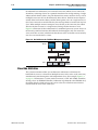
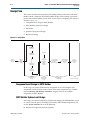
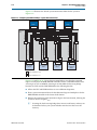
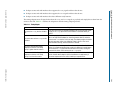
Example System
Figure 1–1 shows an FPGA design that includes an SOPC Builder system and custom
logic modules. You can integrate custom logic inside or outside the SOPC Builder
system. In this example, the custom component inside the SOPC Builder system
communicates with other modules through an Avalon-MM master interface. The
custom logic outside of the SOPC Builder system is connected to the SOPC Builder
system through a PIO interface. The SOPC Builder system includes two SOPC Builder
components with Avalon-ST source and sink interfaces. The system interconnect
fabric connects all of the SOPC Builder components using the Avalon-MM or
Avalon-ST system interconnect as appropriate.
Figure 1–1. Example of an FPGA with a SOPC Builder System Generated by SOPC Builder
Printed Circuit Board
FPGA
System Module
Custom
Logic
Bus Bridge
December 2010
Altera Corporation
DDR2
Memory
Custom
Component
Processor
(32-bit
Master)
Streaming
Data
Sink
M
M
SNK
System Interconnect Fabric
S
S
SRC
PIO
(8-bit
slave)
DDR2
Memory
Controller
Streaming
Data
Source
Co-Processor
DDR2
2
Memory
M
Avalon-MM Master Port
S
Avalon-MM Slave Port
SRC
Avalon-ST Source Port
SNK
Avalon-ST Sink Port
SOPC Builder User Guide
1–4
Chapter 1: Introduction to SOPC Builder
Architecture of SOPC Builder Systems
A component can be a logical device that is entirely contained within the SOPC
Builder system, such as the processor component shown in Figure 1–1. Alternately, a
component can act as an interface to an off-chip device, such as the DDR2 interface
component in Figure 1–1. In addition to the Avalon interface, a component can have
other signals that connect to logic outside the SOPC Builder system. Non-Avalon
signals can provide a special-purpose interface to the SOPC Builder system, such as
the PIO in Figure 1–1. These non-Avalon signals are described in Conduit Interface
chapter in the Avalon Interface Specifications.
Available Components
Altera and third-party developers provide ready-to-use SOPC Builder components,
including:
■
Microprocessors, such as the Nios II processor
■
Microcontroller peripherals, such as a Scatter-Gather DMA Controller and timer
■
Serial communication interfaces, such as a UART and a serial peripheral interface
(SPI)
■
General purpose I/O
■
Communications peripherals, such as a 10/100/1000 Ethernet MAC
■
Interfaces to off-chip devices
Custom Components
You can import HDL modules and entities that you write using Verilog HDL or
VHDL into SOPC builder as custom components. You use the following design flow
to integrate custom logic into an SOPC Builder system:
1. Determine the interfaces used to interact with your custom component.
2. Create the component logic using either Verilog HDL or VHDL.
3. Use the SOPC Builder component editor to create an SOPC Builder component
with your HDL files.
4. Instantiate your component in the system.
Once you have created an SOPC Builder component, you can use the component in
other SOPC Builder systems, and share the component with other design teams.
f For instructions on developing a custom SOPC Builder component, the details about
the file structure of a component, or the component editor, refer to Chapter 4, SOPC
Builder Components.
f For details on the Avalon-MM interface refer to Chapter 2, System Interconnect Fabric
for Memory-Mapped Interfaces. For details on the Avalon-ST interface, refer to
Chapter 3, System Interconnect Fabric for Streaming Interfaces.
SOPC Builder User Guide
December 2010 Altera Corporation
Chapter 1: Introduction to SOPC Builder
Functions of SOPC Builder
1–5
Third-Party Components
You can also use SOPC-ready components that were developed by third-parties.
Altera awards the SOPC Builder Ready certification to IP functions that are ready to
integrate with the Nios II embedded processor or the system interconnect fabric via
SOPC Builder. These cores support the Avalon-MM interface or the Avalon Streaming
(Avalon-ST) interface and may include constraints, software drivers, simulation
models, and reference designs when applicable.
To find SOPC Builder Ready third-party components that you can purchase and use
in SOPC Builder systems, complete the following steps:
1. On the Tools menu in SOPC Builder, click Download Components.
2. On the Intellectual Property Solutions web page, type SOPC Builder ready r in
the box labeled Search for IP, Development Kits and Reference Designs.
Functions of SOPC Builder
This section describes the functions of SOPC Builder.
Defining and Generating the System Hardware
SOPC Builder allows you to design the structure of a hardware system. The GUI
allows you to add components to a system, configure the components, and specify
connectivity.
After you add and parameterize components, SOPC Builder generates the system
interconnect fabric, and outputs HDL files to your project directory. During system
generation, SOPC Builder creates the following items:
■
An HDL file for the top-level SOPC Builder system and for each component in the
system. The top-level HDL file is named <system_name>.v for Verilog HDL designs
and <system_name>.vhd for VHDL designs.
■
Synopsis Design Constraints file (.sdc) for timing analysis.
■
A Block Symbol File (.bsf) representation of the top-level SOPC Builder system for
use in Quartus II Block Diagram Files (.bdf).
■
An example of an instance of the top-level HDL file, <SOPC_project_name_inst>.v
or <SOPC_project_name_inst>.vhd, which demonstrates how to instantiate the
top-level HDL file in your code.
■
A data sheet called <system_name>.html that provides a system overview
including the following information:
■
December 2010
■
All external connections for the system
■
A memory map showing the address of each Avalon-MM slave with respect to
each Avalon-MM master to which it is connected
■
All parameter assignments for each component
A functional test bench for the SOPC Builder system and ModelSim® simulation
project files
Altera Corporation
SOPC Builder User Guide
1–6
Chapter 1: Introduction to SOPC Builder
SOPC Builder Design Flow
■
SOPC information file (.sopcinfo) that describes all of the components and
connections in your system. This file is a complete system description, and is used
by downstream tools such as the Nios II tool chain. It also describes the
parameterization of each component in the system; consequently, you can parse its
contents to get requirements when developing software drivers for SOPC Builder
components.
■
A Quartus II IP File (.qip) that provides the Quartus II software with all required
information about your SOPC Builder system. The .qip file includes references to
the following information:
■
HDL files used in the SOPC Builder system
■
TimeQuest Timing Analyzer Synopsys Design Constraint (.sdc) files
■
Component definition files for archiving purposes
After you generate the SOPC Builder system, you can compile it with the Quartus II
software, or you can instantiate it in a larger FPGA design.
Creating a Memory Map for Software Development
When your SOPC Builder system includes a Nios II processor, SOPC Builder
generates a header file, cpu.h, that provides the base address of each Avalon-MM
slave component. In addition, each slave component can provide software drivers
and other software functions and libraries for the processor. You can create C header
files for your system using the sopc-create-header-files utility.
f For details type sopc-create-header-files --help in a Nios II Command shell.
f For more details about how to provide Nios II software drivers for components, refer
to the Developing Device Drivers for the Hardware Abstraction Layer chapter of the Nios II
Software Developer’s Handbook. The Nios II EDS is separate from SOPC Builder, but it
uses the output of SOPC Builder as the foundation for software development.
Creating a Simulation Model and Test Bench
You can simulate your system after generating it with SOPC Builder. During system
generation, SOPC Builder outputs a simulation test bench and a ModelSim setup
script that eases the system simulation effort. The test bench does the following:
■
Instantiates the SOPC Builder system
■
Drives all clocks and resets
■
Instantiates simulation models for off-chip devices when available
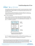
SOPC Builder Design Flow
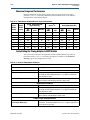
Figure 1–2 illustrates an example bottom-up design flow in SOPC Builder which
starts with component design. As this flow diagram illustrates, the typical design flow
includes the following high-level steps:
1. Package your component for SOPC Builder using the Component Editor.
SOPC Builder User Guide
December 2010 Altera Corporation
Chapter 1: Introduction to SOPC Builder
SOPC Builder Design Flow
1–7
2. Simulate at the unit-level, possibly incorporating Avalon BFMs to verify the
system.
3. Complete the SOPC Builder design by adding other components, specifying
interrupts, clocks, resets, and addresses.
4. Generate the SOPC Builder system.
5. Perform system level simulation.
6. Constrain and compile the design.
7. Download the design to an Altera device.
8. Test in hardware.
Figure 1–2. Complete Qsys Design Flow
1
2
Package Component
Using Component Editor
Simulation at Unit-Level,
Possibly Using Avalon BFMs
Does
Simulation Give
Expected Results?
Yes
No
3
4
5
6
Debug Design
Complete System, Adding
Components, IRQs, Addrs
Generate SOPC BuilderFid
System
Perform System-Level
Simulation
Yes
8
9
No
December 2010
Debug Design
Altera Corporation
Download .sof to PCB
with Altera FPGA
Does
HW Testing Give
Expected Results?
Does
Simulation Give
Expected Results?
7
Constraint, Compile
in Quartus II Generating .sof
Yes
SOPC Builder
System Complete
No
10
Modify Design or
Constraints
SOPC Builder User Guide
1–8
Chapter 1: Introduction to SOPC Builder
Visualization of SOPC Builder Systems
1
In the alternative top-down valid design flow, you begin by designing the SOPC
Builder system and then define and instantiate custom SOPC Buildder component.
This approach clarifies the system requirements earlier in the design process.
Designs targeting HardCopy devices are require specific design constraints.
Consequently, if you are targeting a HardCopy series device, you must verify you
design for the HardCopy companion device.
Follow these guidelines to verify your design for both devices:
1. In the Quartus II Device dialog box, select both the FPGA and the appropriate
HardCopy companion device.
2. In Step 8 of the design flow shown in Figure 1–2, compile for both the FPGA and
HardCopy device.
3. After Step 10 of the design flow shown in Figure 1–2, if FPGA passes all functional
simulation and hardware verification tests, generate the HardCopy handoff
archive and send this archive to the HardCopy Design Center for the backend flow
and tapeout.
Visualization of SOPC Builder Systems
You can use the Filters dialog box to customize the display of your system in the
connections panel. You can filter the display of your system by interface type, instance
name, interface type, or using custom tags. For example, you can use filtering to view
only instances that include an Avalon-MM interface or instances that are connected to
a particular Nios II processor. For more information, refer to Quartus II online Help.
Operating System Support
SOPC Builder supports all of the operating systems that the Quartus II software
supports.
f For details on installation and licensing, refer to the Altera Software Installation and
Licensing Manual.
Talkback Support
Talkback is a Quartus II software feature that provides feedback to Altera on tool and
IP feature usage. Altera uses the data to help guide future product planning efforts.
Talkback sends Altera information on the Altera components you use, including:
interface types, interface properties, parameter names and values, clocking, and
software assignments. For components from Altera, Talkback sends the component
parameter values to help understand what features of the component are being used.
For non-Altera components, Talkback collects information about how interfaces such
as Avalon-MM are being used. Connectivity between components is not sent. The
Talkback file does not include information about system connectivity, interrupts, or
the memory map seen by each master in the system. Talkback collects the same very
general information about your proprietary components.
The Talkback feature is enabled by default. You can disable Talkback from within the
Quartus II software if you do not wish to share your usage data with Altera.
SOPC Builder User Guide
December 2010 Altera Corporation
2. System Interconnect Fabric for
Memory-Mapped Interfaces
The system interconnect fabric for memory-mapped interfaces is a high-bandwidth
interconnect structure for connecting components that use the Avalon®
Memory-Mapped (Avalon-MM) interface. The system interconnect fabric consumes
less logic, provides greater flexibility, and higher throughput than a typical shared
system bus. It is a cross-connect fabric and not a tristated or time domain multiplexed
bus. This chapter describes the functions of system interconnect fabric for
memory-mapped interfaces and the implementation of those functions.
High-Level Description
The system interconnect fabric is the collection of interconnect and logic resources
that connects Avalon-MM master and slaves on components in a system. SOPC
Builder generates the system interconnect fabric to match the needs of the
components in a system. The system interconnect fabric implements the connection
details of a system. It guarantees that signals are routed correctly between master and
slaves, as long as the ports adhere to the rules of the Avalon Interface Specifications. This
chapter provides information on the following topics:
■
“Address Decoding” on page 2–3
■
“Datapath Multiplexing” on page 2–4
■
“Wait State Insertion” on page 2–5
■
“Pipelined Read Transfers” on page 2–6
■
“Dynamic Bus Sizing and Native Address Alignment” on page 2–6
■
“Arbitration for Multimaster Systems” on page 2–9
■
“Burst Adapters” on page 2–14
■
“Interrupts” on page 2–15
■
“Reset Distribution” on page 2–16
f For details about the Avalon-MM interface, refer to the Avalon Interface Specifications.
System interconnect fabric for memory-mapped interfaces supports the following
items:
December 2010
■
Any number of master and slave components. The master-to-slave relationship
can be one-to-one, one-to-many, many-to-one, or many-to-many.
■
On-chip components.
■
Interfaces to off-chip devices.
■
Master and slaves of different data widths.
■
Components operating in different clock domains.
■
Components using multiple Avalon-MM ports.
Altera Corporation
SOPC Builder User Guide
2–2
Chapter 2: System Interconnect Fabric for Memory-Mapped Interfaces
High-Level Description
Figure 2–1 shows a simplified diagram of the system interconnect fabric in an
example memory-mapped system with multiple masters.
1
All figures in this chapter are simplified to show only the particular function being
discussed. In a complete system, the system interconnect fabric might alter the
address, data, and control paths beyond what is shown in any one particular figure.
Figure 2–1. System Interconnect Fabric—Example System
S
Control
Processor
Instruction
M
DMA Controller
Data
M
Read
M
Write
M
MUX
System
Interconnect
Fabric
Arbiter
Arbiter
Tri-State Bridge
S
S
S
Instruction
Memory
Data
Memory
SDRAM
Controller
S
S
Ethernet
MAC/PHY
Chip
Flash
Memory
Chip
SDRAM Chip
Write Data & Control Signals
M
Avalon-MM Master Port
S
Avalon-MM Slave Port
Read Data
Interface to Off-Chip Device
SOPC Builder supports components with multiple Avalon-MM interfaces, such as the
processor component shown in Figure 2–1. Because SOPC Builder can create system
interconnect fabric to connect components with multiple interfaces, you can create
complex interfaces that provide more functionality than a single Avalon-MM
interface. For example, you can create a component with two different Avalon-MM
slaves, each with an associated interrupt interface.
System interconnect fabric can connect any combination of components, as long as
each interface conforms to the Avalon Interface Specifications. It can, for example,
connect a system comprised of only two components with unidirectional dataflow
between them. Avalon-MM interfaces are suitable for random address transactions,
such as to memories or embedded peripherals.
SOPC Builder User Guide
December 2010 Altera Corporation
Chapter 2: System Interconnect Fabric for Memory-Mapped Interfaces
Fundamentals of Implementation
2–3
Generating system interconnect fabric is SOPC Builder’s primary purpose. In most
cases, you are not required to modify the generated HDL; however, a basic
understanding of how HDL works can help you optimize your system. For example,
knowledge of the arbitration algorithm can help designers of multimaster systems
minimize the impact of arbitration on the system throughput.
Fundamentals of Implementation
System interconnect fabric for memory-mapped interfaces implements a partial
crossbar interconnect structure that provides concurrent paths between master and
slaves. System interconnect fabric consists of synchronous logic and routing resources
inside the FPGA.
For each component interface, system interconnect fabric manages Avalon-MM
transfers, interacting with signals on the connected component. Master and slave
interfaces can contain different signals and the system interconnect fabric handle any
adaptation necessary between them. In the path between master and slaves, the
system interconnect fabric might introduce registers for timing synchronization, finite
state machines for event sequencing, or nothing at all, depending on the services
required by the specific interfaces.
f For more information, refer to the Avalon Memory-Mapped Design Optimizations
chapter in the Embedded Design Handbook.
Functions of System Interconnect Fabric
System interconnect fabric logic provides the following functions:
■
“Address Decoding” on page 2–3
■
“Datapath Multiplexing” on page 2–4
■
“Wait State Insertion” on page 2–5
■
“Pipelined Read Transfers” on page 2–6
■
“Arbitration for Multimaster Systems” on page 2–9
■
“Burst Adapters” on page 2–14
■
“Interrupts” on page 2–15
■
“Reset Distribution” on page 2–16
The behavior of these functions in a specific SOPC Builder system depends on the
design of the components in the system and the settings made in SOPC Builder. The
remaining sections of this chapter describe how SOPC Builder implements each
function.
Address Decoding
Address decoding logic in the system interconnect fabric forwards appropriate
addresses to each slave. Address decoding logic simplifies component design in the
following ways:
December 2010
Altera Corporation
SOPC Builder User Guide
2–4
Chapter 2: System Interconnect Fabric for Memory-Mapped Interfaces
Datapath Multiplexing
■
The system interconnect fabric selects a slave whenever it is being addressed by a
master. Slave components do not need to decode the address to determine when
they are selected.
■
Slave addresses are properly aligned to the slave interface.
■
Changing the system memory map does not involve manually editing HDL.
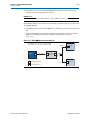
Figure 2–2 shows a block diagram of the address-decoding logic for one master and
two slaves. Separate address-decoding logic is generated for every master in a system.
As Figure 2–2 shows, the address decoding logic handles the difference between the
master address width (<M>) and the individual slave address widths (<S> and <T>).
It also maps only the necessary master address bits to access words in each slave’s
address space.
Figure 2–2. Block Diagram of Address Decoding Logic
address [M..0]
Master
Port
Address
Decoding
Logic
read/write
address [S..0]
Slave
Port 1
(8-bit)
read/write
Slave
Port 2
(32-bit)
address [T..2]
In SOPC Builder, the user-configurable aspects of address decoding logic are
controlled by the Base setting in the list of active components on the System Contents
tab, as shown in Figure 2–3.
Figure 2–3. Base Settings in SOPC Builder Control Address Decoding
Datapath Multiplexing
Datapath multiplexing logic in the system interconnect fabric drives the writedata
signal from the granted master to the selected slave, and the readdata signal from the
selected slave back to the requesting master.
SOPC Builder User Guide
December 2010 Altera Corporation
Chapter 2: System Interconnect Fabric for Memory-Mapped Interfaces
Wait State Insertion
2–5
Figure 2–4 shows a block diagram of the datapath multiplexing logic for one master
and two slaves. SOPC Builder generates separate datapath multiplexing logic for
every master in the system.
Figure 2–4. Block Diagram of Datapath Multiplexing Logic
readdata1
Slave
Port 1
address
Data
Path
Multiplexer
readdata
Master
Port
writedata
control
Slave
Port 2
readdata2
In SOPC Builder, the generation of datapath multiplexing logic is specified using the
connections panel on the System Contents tab.
Wait State Insertion
Wait states extend the duration of a transfer by one or more cycles. Wait state insertion
logic accommodates the timing needs of each slave, and causes the master to wait
until the slave can proceed. System interconnect fabric inserts wait states into a
transfer when the target slave cannot respond in a single clock cycle. System
interconnect fabric also inserts wait states in cases when slave read_enable and
write_enable signals have setup or hold time requirements.
Wait state insertion logic is a small finite-state machine that translates control signal
sequencing between the slave side and the master side. Figure 2–5 shows a block
diagram of the wait state insertion logic between one master and one slave.
Figure 2–5. Block Diagram of Wait State Insertion Logic
read/write
Wait-State
Insertion
Logic
read/write
wait request
Master
Port
address
Slave
Port
data
System interconnect fabric can force a master to wait for several reasons in addition to
the wait state needs of a slave. For example, arbitration logic in a multimaster system
can force a master to wait until it is granted access to a slave.
December 2010
Altera Corporation
SOPC Builder User Guide
2–6
Chapter 2: System Interconnect Fabric for Memory-Mapped Interfaces
Pipelined Read Transfers
SOPC Builder generates wait state insertion logic based on the properties of all slaves
in the system.
Pipelined Read Transfers
The Avalon-MM interface supports pipelined read transfers, allowing a pipelined
master to start multiple read transfers in succession without waiting for the prior
transfers to complete. Pipelined transfers allow master-slave pairs to achieve higher
throughput, even though the slave requires one or more cycles of latency to return
data for each transfer.
SOPC Builder generates system interconnect fabric with pipeline management logic
to take advantage of pipelined components wherever possible, based on the pipeline
properties of each master-slave pair in the system. Regardless of the pipeline latency
of a target slave, SOPC Builder guarantees that read data arrives at each master in the
order requested. Because master and slaves often have mismatched pipeline latency,
system interconnect fabric often contains logic to reconcile the differences. Many cases
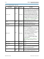
of pipeline latency are possible, as shown in Table 2–1.
Table 2–1. Various Cases of Pipeline Latency in a Master-Slave Pair
Master
Slave
Pipeline Management Logic Structure
No pipeline
The system interconnect fabric does not instantiate logic to handle pipeline
latency.
No pipeline
Pipelined with fixed
or variable latency
The system interconnect fabric forces the master to wait through any slave-side
latency cycles. This master-slave pair gains no benefits of pipelining, because
the master waits for each transfer to complete before beginning a new transfer.
However, while the master is waiting, the slave can accept transfers from a
different master.
Pipelined
No pipeline
The system interconnect fabric carries out the transfer as if neither master nor
slave were pipelined, causing the master to wait until the slave returns data.
Pipelined
Pipelined with fixed
latency
The system interconnect fabric allows the master to capture data at the exact
clock cycle when data from the slave is valid. This process enables the
master-slave pair to achieve maximum throughput performance.
Pipelined
Pipelined with
variable latency
This is the simplest pipelined case, in which the slave asserts a signal when its
readdata is valid, and the master captures the data. This case enables this
master-slave pair to achieve maximum throughput.
No pipeline
SOPC Builder generates logic to handle pipeline latency based on the properties of the
master and slaves in the system. When configuring a system in SOPC Builder, there
are no settings that directly control the pipeline management logic in the system
interconnect fabric.
Dynamic Bus Sizing and Native Address Alignment
SOPC Builder generates system interconnect fabric to accommodate master and
slaves with unmatched data widths. Address alignment affects how slave data is
aligned in a master's address space, in the case that the master and slave data widths
are different. Address alignment is a property of each slave, and can be different for
each slave in a system. A slave can declare itself to use one of the following:
■
SOPC Builder User Guide
Dynamic bus sizing
December 2010 Altera Corporation
Chapter 2: System Interconnect Fabric for Memory-Mapped Interfaces
Dynamic Bus Sizing and Native Address Alignment
■
2–7
Native address alignment
The following sections explain the implications of the address alignment property
slave devices.
Dynamic Bus Sizing
Dynamic bus sizing hides the details of interfacing a narrow component device to a
wider master, and vice versa. When an <N>-bit master accesses a slave with dynamic
bus sizing, the master operates exclusively on full <N>-bit words of data, without
awareness of the slave data width.
1
When using dynamic bus sizing, the slave data width in units of bytes must be a
power of two.
Dynamic bus sizing provides the following benefits:
■
Eliminates the need to create address-alignment hardware manually.
■
Reduces design complexity of the master component.
■
Enables any master to access any memory device, regardless of the data width.
In the case of dynamic bus sizing, the system interconnect fabric includes a small
finite state machine that reconciles the difference between master and slave data
widths. The behavior is different depending on whether the master data width is
wider or narrower than the slave.
Wider Master
In the case of a wider master, the dynamic bus-sizing logic accepts a single, wide
transfer on the master side, and then performs multiple narrow transfers on the slave
side. For a data-width ratio of <N>:1, the dynamic bus-sizing logic generates up to
<N> slave transfers for each master transfer. The master waits while multiple
slave-side transfers complete; the master transfer ends when all slave-side transfers
end.
Dynamic bus-sizing logic uses the master-side byte-enable signals to generate
appropriate slave transfers. The dynamic bus-sizing logic performs as many
slave-side transfers as necessary to write or read the specified byte lanes.
Narrower Master
In the case of a narrower master, one transfer on the master side generates one
transfer on the slave side. In this case, multiple master word addresses map to a single
offset in the slave memory space. The dynamic bus-sizing logic maps each master
address to a subset of byte lanes in the appropriate slave offset. All bytes of the slave
memory are accessible in the master address space.
December 2010
Altera Corporation
SOPC Builder User Guide
2–8
Chapter 2: System Interconnect Fabric for Memory-Mapped Interfaces
Dynamic Bus Sizing and Native Address Alignment
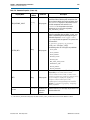
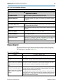
Table 2–2 demonstrates the case of a 32-bit master accessing a 64-bit slave with
dynamic bus sizing. In the table, offset refers to the offset into the slave memory
space.
Table 2–2. 32-Bit Master View of 64-Bit Slave with Dynamic Bus Sizing
32-bit Address
Data
0×00000000 (word 0)
OFFSET[0]31..0
0×00000004 (word 1)
OFFSET[0]63..32
0×00000008 (word 2)
OFFSET[1]31..0
0×0000000C (word 3)
OFFSET[1]63..32
In the case of a read transfer, the dynamic bus-sizing logic multiplexes the appropriate
byte lanes of the slave data to the narrow master. In the case of a write transfer, the
dynamic bus-sizing logic uses slave-side byte-enable signals to write only to the
appropriate byte lanes.
1
Altera recommends that you select dynamic bus sizing whenever possible. Dynamic
bus sizing offers more flexibility when the master and slave components in your
system have different widths.
Native Address Alignment
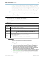
Table 2–3 demonstrates native address alignment and dynamic bus sizing for a 32-bit
master connected to a 16-bit slave (a 2:1 ratio). In this example, the slave is mapped to
base address <BASE> in the master’s address space. In Table 2–3, OFFSET refers to the
offset into the 16-bit slave address space.
Table 2–3. 32-Bit Master View of 16-Bit Slave Data
32-bit Master Address
Data with Native Alignment
Data with Dynamic Bus Sizing
BASE + 0x0 (word 0)
0×0000:OFFSET[0]
OFFSET[1]:OFFSET[0]
BASE + 0x4 (word 1)
0×0000:OFFSET[1]
OFFSET[3]:OFFSET[2]
BASE + 0x8 (word 2)
0×0000:OFFSET[2]
OFFSET[5]:OFFSET[4]
BASE + 0xC (word 3)
0×0000:OFFSET[3]
OFFSET[7]:OFFSET[6]
...
...
...
BASE + 4N (word N)
0×0000:OFFSET[N]
OFFSET[2N+1]:OFFSET[2N]
When connecting a wide master to a narrow slave port that uses native addressing,
the following addressing formula should be used to determine what address to
present to the system interconnect fabric:
<master address> = <slave base address> + (<slave word offset> *
<master data width in bytes>)
For example, a 64-bit master needs to write to the second word of a 32-bit slave that
uses native addressing the formula would reduce to:
<master address> = <slave base address> + (1 * 8)
SOPC Builder User Guide
December 2010 Altera Corporation
Chapter 2: System Interconnect Fabric for Memory-Mapped Interfaces
Arbitration for Multimaster Systems
2–9
SOPC Builder generates appropriate address-alignment logic based on the properties
of the master and slaves in the system. When configuring a system in SOPC Builder,
there are no settings that directly control the address alignment in the system
interconnect fabric.
Arbitration for Multimaster Systems
System interconnect fabric supports systems with multiple master components. In a
system with multiple masters, such as the system pictured in Figure 2–1 on page 2–2,
the system interconnect fabric provides shared access to slaves using a technique
called slave-side arbitration. Slave-side arbitration moves the arbitration logic close to
the slave, such that the algorithm that determines which master gains access to a
specific slave in the event that multiple masters attempt to access the same slave at the
same time.
The multimaster architecture used by system interconnect fabric offers the following
benefits:
■
Eliminates having to create arbitration hardware manually.
■
Allows multiple masters to transfer data simultaneously. Unlike traditional
host-side arbitration architectures where each master must wait until it is granted
access to the shared bus, multiple Avalon-MM masters can simultaneously
perform transfers with independent slaves. Arbitration logic stalls a master only
when multiple masters attempt to access the same slave during the same cycle.
■
Eliminates unnecessary master-slave connections. The connection between a
master and a slave exists only if it is specified in SOPC Builder. If a master never
initiates transfers to a specific slave, no connection is necessary, and therefore
SOPC Builder does not waste logic resources to connect the two ports.
■
Provides configurable arbitration settings, and arbitration for each slave is
specified independently. For example, you can grant one master more arbitration
shares than others, allowing it to gain more access cycles to the slave. The
arbitration share settings are defined for each slave independently.
■
Simplifies master component design. The details of arbitration are encapsulated
inside the system interconnect fabric. Each Avalon-MM master connects to the
system interconnect fabric as if it is the only master in the system. As a result, you
can reuse a component in single-master and multimaster systems without
requiring design changes to the component.
Traditional Shared Bus Architectures
This section discusses the architecture of the system interconnect fabric generated by
SOPC Builder for multimaster systems. As a frame of reference for the discussion of
multiple masters and arbitration, this section describes traditional bus architectures.
December 2010
Altera Corporation
SOPC Builder User Guide
2–10
Chapter 2: System Interconnect Fabric for Memory-Mapped Interfaces
Arbitration for Multimaster Systems
In traditional bus architectures, one or more bus masters and bus slaves connect to a
shared bus, consisting of wires on a printed circuit board or on-chip routing. A single
arbiter controls the bus (that is, the path between bus masters and bus slaves), so that
multiple bus masters do not simultaneously drive the bus. Each bus master requests
control of the bus from the arbiter, and the arbiter grants access to a single master at a
time. Once a master has control of the bus, the master performs transfers with any bus
slave. When multiple masters attempt to access the bus at the same time, the arbiter
allocates the bus resources to a single master, forcing all other masters to wait.
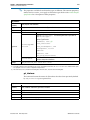
Figure 2–6 illustrates the bus architecture for a traditional processor system. Access to
the shared system bus becomes the bottleneck for throughput: only one master has
access to the bus at a time, which means that other masters are forced to wait and only
one slave can transfer data at a time.
Figure 2–6. Bus Architecture in a Traditional Microprocessor System
Masters
Master 2
DMA
Controller
Master 1
System CPU
Arbiter
Bottleneck
System Bus
Slaves
UART
PIO
Program
Memory
Data
Memory
Slave-Side Arbitration
The system interconnect fabric uses multimaster architecture to eliminate the
bottleneck for access to a shared bus. Multiple masters can be active at the same time,
simultaneously transferring data with independent slaves. For example, Figure 2–1
on page 2–2 demonstrates a system with two masters (a CPU and a DMA controller)
sharing a slave (an SDRAM controller). Arbitration is performed at the SDRAM slave;
the arbiter dictates which master gains access to the slave if both masters initiate a
transfer with the slave in the same cycle.
SOPC Builder User Guide
December 2010 Altera Corporation
Chapter 2: System Interconnect Fabric for Memory-Mapped Interfaces
Arbitration for Multimaster Systems
2–11
Figure 2–7 focuses on the two masters and the shared slave and shows additional
detail of the data, address, and control paths. The arbiter logic multiplexes all address,
data, and control signals from a master to a shared slave.
Figure 2–7. Detailed View of Multimaster Connections
M1 Address
Request Control
M2 Address
Address
Arbiter
Master 1
M1 Write Data
Write Data
Slave
Control
M2 Write Data
Request Control
Master 2
Slave Read Data
Arbiter Details
SOPC Builder generates an arbiter for every slave, based on arbitration parameters
specified in SOPC Builder. The arbiter logic performs the following functions for its
slave:
December 2010
■
Evaluates the address and control signals from each master and determines which
master, if any, gains access to the slave next.
■
Grants access to the chosen master and forces all other requesting masters to wait.
■
Uses multiplexers to connect address, control, and datapaths between the multiple
masters and the slave.
Altera Corporation
SOPC Builder User Guide
2–12
Chapter 2: System Interconnect Fabric for Memory-Mapped Interfaces
Arbitration for Multimaster Systems
Figure 2–8 shows the arbiter logic in an example multimaster system with two
masters, each connected to two slaves.
Figure 2–8. Block Diagram of Arbiter Logic
S1 Read Data & Control
Data-Path
Multiplexing
Logic
Master 1
(M1)
M1 wait
M2 wait
Slave 1
Arbiter Master Select
M1 Address, Write
Data & Control
Slave 1
(S1)
M2 Address, Write
Data & Control
Slave 2
(S2)
Data-Path
Multiplexing
Logic
Master 2
(M2)
Slave 2
Arbiter
M1 wait
M2 wait
Master Select
S2 Read Data & Control
Arbitration Rules
This section describes the rules by which the arbiter grants access to masters when
they contend.
Setting Arbitration Parameters in SOPC Builder
You specify the arbitration shares for each master using the connection panel on the
System Contents tab of SOPC Builder, as shown in Figure 2–9.
Figure 2–9. Arbitration Settings on the System Contents Tab
The arbitration settings are hidden by default. To see them, on the View menu, click
Show Arbitration.
SOPC Builder User Guide
December 2010 Altera Corporation
Chapter 2: System Interconnect Fabric for Memory-Mapped Interfaces
Arbitration for Multimaster Systems
2–13
Fairness-Based Shares
Arbiter logic uses a fairness-based arbitration scheme. In a fairness-based arbitration
scheme, each master pair has an integer value of transfer shares with respect to a slave.
One share represents permission to perform one transfer.
For example, assume that two masters continuously attempt to perform back-to-back
transfers to a slave. Master 1 is assigned three shares and Master 2 is assigned four
shares. In this case, the arbiter grants Master 1 access for three transfers, then Master 2
for four transfers. This cycle repeats indefinitely. Figure 2–10 demonstrates this case,
showing each master’s transfer request output, wait request input (which is driven by
the arbiter logic), and the current master with control of the slave.
Figure 2–10. Arbitration of Continuous Transfer Requests from Two Masters
clk
M1_transfer_request
M1_waitrequest
M2_transfer_request
M2_waitrequest
Current_Master
Master 1
Master 2
Master 1
Master 2
Master 1
If a master stops requesting transfers before it exhausts its shares, it forfeits all its
remaining shares, and the arbiter grants access to another requesting master. Refer to
Figure 2–11. After completing one transfer, Master 2 stops requesting for one clock
cycle. As a result, the arbiter grants access back to Master 1, which gets a replenished
supply of shares.
Figure 2–11. Arbitration of Two Masters with a Gap in Transfer Requests
clk
M1_transfer_request
M1_waitrequest
M2_transfer_request
M2_waitrequest
Current_Master
Master 1
Master 2
Master 1
Master 2
Master 1
Master 2
Round-Robin Scheduling
When multiple masters contend for access to a slave, the arbiter grants shares in
round-robin order. Round-robin scheduling drives a request interface according to
space available and data available credit interfaces. At every slave transfer, only
requesting masters are included in the arbitration.
December 2010
Altera Corporation
SOPC Builder User Guide
2–14
Chapter 2: System Interconnect Fabric for Memory-Mapped Interfaces
Burst Adapters
Burst Transfers
Avalon-MM burst transfers grant a master uninterrupted access to a slave for a
specified number of transfers. The master specifies the number of transfers when it
initiates the burst. Once a burst begins between a master-slave pair, arbiter logic does
not allow any other master to access the slave until the burst completes. For burst
masters, the size of the burst determines the number of cycles that the master has
access to the slave, and the selected arbitration shares have no effect.
Burst Adapters
System interconnect fabric provides burst adaptation logic to accommodate the burst
capabilities of each port in the system, including ports that do not support burst
transfers. Burst adaptation logic consists of a finite state machine that translates the
sequencing of address and control signals between the slave side and the master side.
The maximum burst length for each port is determined by the component design and
is independent of other ports in the system. Therefore, a particular master might be
capable of initiating a burst longer than a slave’s maximum supported burst length. In
this case, the burst management logic translates the master burst into smaller slave
bursts, or into individual slave transfers if the slave does not support bursts. Until the
master completes the burst, the arbiter logic prevents other masters from accessing
the target slave.
For example, if a master initiates a burst of 16 transfers to a slave with maximum burst
length of 8, the burst adapter logic initiates two bursts of length 8 to the slave. If the
master initiates a burst of 14, the burst adapter logic segments the burst transfer into a
burst of 8 words followed by a burst of 6 words, because the slave can only handle a
maximum burst length of 8. If a master initiates a burst of 16 transfers to a slave that
does not support bursts, the burst management logic initiates 16 separate transfers to
the slave.
1
The burst adapter inserts one idle cycle at the start of each burst. System throughput is
maximized when burst sizes are as large as possible.
In the case of a non-linewrap burst master connected to a slave with the
linewrapBursts property set to TRUE, it is not always possible to issue the maximumsized burst to the slave. In these cases the burst adapter is not capable of adapting the
master and slave pairing. An adapter is generated; however, if the master performs a
burst transaction to the slave that crosses the slave burst boundary data corruption
can occur. To avoid a functional failure, you should ensure the master posts bursts of
length one until the master burst boundary has been reached. The master burst
boundary has an alignment of <master_data_width> ×
<master_maximum_burst_length>.
Any burst transaction that begins on a master burst boundary is guaranteed to not
cross the burst boundary of the slave port regardless of the slave port's maximum
burst length. Typically the only Avalon-MM interfaces that support burst wrapping
are burst capable SDRAM controllers.
f For more information about the linewrapBursts property, refer to the Avalon MemoryMapped Slave Interfaces chapter in the Avalon Interface Specifications.
SOPC Builder User Guide
December 2010 Altera Corporation
Chapter 2: System Interconnect Fabric for Memory-Mapped Interfaces
Interrupts
2–15
Interrupts
In systems where components have interrupt request (IRQ) sender interfaces, the
system interconnect fabric includes interrupt controller logic. A separate interrupt
controller is generated for each interrupt receiver. The interrupt controller aggregates
IRQ signals from all interrupt senders, and maps them to user-specified values on the
receiver inputs.
f For further information, refer to the Interrupt Interfaces chapter in the Avalon Interface
Specifications.
Individual Requests IRQ Scheme
In the individual requests IRQ scheme, the system interconnect fabric passes IRQs
directly from the sender to the receiver, without making any assumptions about IRQ
priority. In the event that multiple senders assert their IRQs simultaneously, the
receiver logic (presumably under software control) determines which IRQ has highest
priority, then responds appropriately.
Using individual requests, the interrupt controller can handle up to 32 IRQ inputs.
The interrupt controller generates a 32-bit signal irq[31:0] to the receiver, and simply
maps slave IRQ signals to the bits of irq[31:0]. Any unassigned bits of irq[31:0] are
disabled. Figure 2–12 shows an example of the interrupt controller mapping the IRQs
on four senders to irq[31:0] on a receiver.
Figure 2–12. IRQ Mapping Using Software Priority
Sender
1
irq
Interrupt
Controller
Sender
2
irq
Sender
3
irq
irq0
irq1
irq2
irq3
irq4
irq5
irq6
Receiver
irq31
Sender
4
irq
Priority Encoded Interrupt Scheme
In the priority encoded interrupt scheme, in the event that multiple slaves assert their
IRQs simultaneously, the system interconnect fabric provides the interrupt receiver
with a 1-bit interrupt signal, and the number of the highest priority active interrupt.
An IRQ of lesser priority is undetectable until all IRQs of higher priority have been
serviced.
December 2010
Altera Corporation
SOPC Builder User Guide
2–16
Chapter 2: System Interconnect Fabric for Memory-Mapped Interfaces
Reset Distribution
Using priority encoded interrupts, the interrupt controller can handle up to 64 slave
IRQ signals. The interrupt controller generates a 1-bit irq signal to the receiver,
signifying that one or more senders have generated an IRQ. The controller also
generates a 6-bit irqnumber signal, which outputs the encoded value of the highest
pending IRQ. See Figure 2–13.
Figure 2–13. IRQ Mapping Using Hardware Priority
Sender
1
irq
Sender
2
irq
Sender
3
irq
Interrupt
Controller
irq
Receiver
Sender
4
irq
irq0
irq1
irq2
irq3
irq4
irq5
irq6
irqnumber [5..0]
Priority
Encoder
irq63
Assigning IRQs in SOPC Builder
You specify IRQ settings on the System Contents tab of SOPC Builder. After adding
all components to the system, you make IRQ settings for all interrupt senders, with
respect to each interrupt receiver. For each slave, you can either specify an IRQ
number, or specify not to connect the IRQ.
Reset Distribution
SOPC Builder generates the logic used in the system interconnect fabric, which drives
the reset pulse to all the logic. The system interconnect fabric distributes the reset
signal conditioned for each clock domain. The duration of the reset signal is at least
one clock period.
The system interconnect fabric asserts the system-wide reset in the following
conditions:
■
The global reset input to the SOPC Builder system is asserted.
■
Any component asserts its resetrequest signal.
The global reset and reset requests are ORed together. This signal is then synchronized
to each clock domain associated to an Avalon-MM port, which causes the
asynchronous resets to be de-asserted synchronously.
SOPC Builder User Guide
December 2010 Altera Corporation
3. System Interconnect Fabric for
Streaming Interfaces
The interconnect fabric for Avalon® Streaming connects high-bandwidth, low latency
components that use the Avalon Streaming (Avalon-ST) interface. This interconnect
fabric creates datapaths for unidirectional traffic including multichannel streams,
packets, and DSP data. This chapter describes the Avalon-ST interconnect fabric and
its use in connecting components with Avalon-ST interfaces. Descriptions of specific
adapters and their use in streaming systems can be found in the following sections:
■
“Adapters” on page 3–3
■
“Multiplexer Examples” on page 3–5
High-Level Description
Avalon-ST interconnect fabric is logic generated by SOPC Builder. Using SOPC
Builder, you specify how Avalon-ST source and sink ports connect. SOPC Builder
then creates a high performance point-to-point interconnect between the two
components. The Avalon-ST interconnect is flexible and can be used to implement
on-chip interfaces for industry standard telecommunications and data
communications cores, such as Ethernet IEEE 802.3 MAC and SPI 4.2. In all cases, bus
widths, packets, and error conditions are custom-defined.
Figure 3–1 illustrates the simplest system example that generates an interconnect
between the source and sink. This source-sink pair includes only the data and valid
signals.
Figure 3–1. Interconnect for a Simple Avalon Streaming Source-Sink Pair
Data
Source
valid
data
Data
Sink
Figure 3–2 illustrates a more extensive interface that includes signals indicating the
start and end of packets, channel numbers, error conditions, and back pressure.
Figure 3–2. Avalon Streaming Interface for Packet Data
Data
Source
December 2010
Altera Corporation
ready
valid
channel
startofpacket
endofpacket
empty
error
data
Data
Sink
SOPC Builder User Guide
3–2
Chapter 3: System Interconnect Fabric for Streaming Interfaces
Avalon Streaming and Avalon Memory-Mapped Interfaces
All data transfers using Avalon-ST interconnect occur synchronously to the rising
edge of the associated clock interface. All outputs from the source interface, including
the data, channel, and error signals, must be registered on the rising edge of the clock.
Registers are not required for inputs at the sink interface. Registering signals only at
the source provides for high frequency operation while eliminating back-to-back
registration with no intervening logic. There is no inherent maximum performance of
the interconnect. Throughput for a system depends on the components and how they
are connected.
f For details about the Avalon-ST interface protocol, refer to the Avalon Interface
Specifications.
Avalon Streaming and Avalon Memory-Mapped Interfaces
The Avalon-ST and Avalon Memory-Mapped (Avalon-MM) interfaces are
complementary. High bandwidth components with streaming data typically use
Avalon-ST interfaces for the high throughput datapath. These components can also
use Avalon-MM connection interfaces to provide an access point for control. In
contrast to the Avalon-MM interconnect, which can be used to create a wide variety of
topologies, the Avalon-ST interconnect fabric always creates a point-to-point between
a single data source and data sink, as Figure 3–3 illustrates. There are two connection
pairs in this figure:
SOPC Builder User Guide
■
The data source in the Rx Interface transfers data to the data sink in the FIFO.
■
The data source in the FIFO transfers data to the Tx Interface data sink.
December 2010 Altera Corporation
Chapter 3: System Interconnect Fabric for Streaming Interfaces
Adapters
3–3
In Figure 3–3, the Avalon-MM interface allows a processor to access the data source,
FIFO or data sink to provide system control.
Figure 3–3. Use of the Avalon Memory-Mapped and Streaming Interfaces
Control Plane Avalon
:
Memory Mapped Inteface
Processor
RAM
UART
Timer
Control
Slave
Control
Slave
Control
Slave
Data Source
(Rx Interface)
FIFO
Data Sink
(Tx Interface)
Data
Data
Source
Source
ready
valid
channel
Data
Sink
data
Data
Source
ready
valid
channel
data
Data
Sink
Data Plane Avalon
:
Streaming Interface
Adapters
Adapters are configurable SOPC Builder components that are part of the streaming
interconnect fabric. They are used to connect source and sink interfaces that are not
exactly the same without affecting the semantics of the data. SOPC Builder includes
the following four adapters:
■
Data Format Adapter
■
Timing Adapter
■
Channel Adapter
■
Error Adapter
You can add Avalon-ST adapters between two components with mismatched
interfaces. The adapter allows you to connect a data source to a data sink of differing
byte sizes. If you connect mismatched Avalon-ST sources and sinks in SOPC Builder
without inserting adapters, SOPC Builder generates error messages. Inserting
adapters into the system does not change the types of components that SOPC Builder
allows you to connect. The Insert Avalon-ST Adapters command on the System
menu attempts to correct these errors automatically, if possible, by inserting the
appropriate adapter types.
December 2010
Altera Corporation
SOPC Builder User Guide
3–4
Chapter 3: System Interconnect Fabric for Streaming Interfaces
Adapters
f For complete information about these adapters, refer to Chapter 12, Avalon Streaming
Interconnect Components.
The following sections provide an overview of these adapters.
Data Format Adapter
The data format adapter allows you to connect interfaces that have different values
for the parameters defining the data signal. One of the most common uses of this
adapter is to convert data streams of different widths. Figure 3–4 shows an adapter
that allows a connection between a 128-bit input data stream and three 32-bit output
data streams.
Figure 3–4. Avalon Streaming Interconnect Fabric with Data Format Adapter
128 bits
128-bit RX 128 bits
Interface
128 bits
Data
Format
Adapter
32 bits
32-bit TX
Interface
Data
Format
Adapter
32 bits
32-bit TX
Interface
Data
Format
Adapter
32 bits
32-bit TX
Interface
Timing Adapter
The timing adapter allows you to connect component interfaces that require a
different number of cycles before driving or receiving data. This adapter inserts a
FIFO between the source and sink to buffer data or pipeline stages to delay the back
pressure signals. The timing adapter can also be used to connect interfaces that
support the ready signal and those that do not.
SOPC Builder User Guide
December 2010 Altera Corporation
Chapter 3: System Interconnect Fabric for Streaming Interfaces
Multiplexer Examples
3–5
Channel Adapter
The channel adapter provides adaptations between interfaces that have different
support for the channel signal or channel-related parameters. For example, if the
source channel is narrower than the sink channel, you can use this adapter to connect
them. The high-order bits of the sink channel are connected to zero. You can also use
this adapter to connect a source with a wider channel to a sink with a narrower
channel. If the source provides data for a channel that the sink cannot receive, the data
is not transferred.
Error Adapter
The error adapter ensures that per-bit error information provided by the source
interface is correctly connected to the sink interface’s input error signal. Matching
error conditions handled by the source and sink are connected. If the source has an
error condition that is not supported by the sink, the signal is left unconnected; the
adapter provides a simulation error message and an error indication if this error is
ever asserted. If the sink has an error condition that is not supported by the source, the
sink’s input is tied to zero.
Multiplexer Examples
You can combine these adapters with streaming components to create datapaths
whose input and output streams have different properties. The following sections
provide examples of datapaths constructed using SOPC Builder in which the output
stream is higher performance than the input stream:
December 2010
■
The first example shows an output with double the throughput of each interface
with a corresponding doubling of the clock frequency.
■
The second example doubles the data width.
■
The third example boosts the frequency of a stream by 10% by multiplexing input
data from two sources.
Altera Corporation
SOPC Builder User Guide
3–6
Chapter 3: System Interconnect Fabric for Streaming Interfaces
Multiplexer Examples
Example to Double Clock Frequency
Figure 3–5 illustrates a datapath that uses the dual clock version of the on-chip FIFO
memory and Avalon-ST channel multiplexer to merge the 100 MHz input from two
streaming data sources into a single 200 MHz streaming output. As Figure 3–5
illustrates, this example increases throughput by increasing the frequency and
combining inputs.
Figure 3–5. Datapath that Doubles the Clock Frequency
On-Chip FIFO
Memory – Dual Clk
Data Source
input
src
100 MHz
src 200 MHz
sink
sink
src
On-Chip FIFO
Memory – Dual Clk
Data Source
input
src 100 MHz
sink
sink
src 200 MHz
output
200 MHz
sink
Example to Double Data Width and Maintain Frequency
Figure 3–6 illustrates a datapath that uses the data format adapter and Avalon-ST
channel multiplexer to convert two, 8-bit inputs running at 100 MHz to a single 16-bit
output at 100 MHz.
Figure 3–6. Datapath to Double Data Width and Maintain Original Frequency
Data Source
input
src
Data Format
8 bits
sink
Adapter
@100 MHz
src
16 bits
sink
@100 MHz
src
16 bits
@100 MHz
Data Source
input
src
Data Format
8 bits
sink
Adapter
sink
@100 MHz
src
16 bits
@100 MHz sink
Example to Boost the Frequency
Figure 3–7 illustrates a datapath that uses the dual clock version of the on-chip FIFO
memory to boost the frequency of input data from 100 MHz to 110 MHz by sampling
two input streams at differential rates. In this example, the on-chip FIFO memory has
an input clock frequency of 100 MHz and an output clock frequency of 110 MHz. The
channel multiplexer runs at 110 MHz and samples one input stream 27.3 percent of
the time and the second 72.7 percent of the time.
SOPC Builder User Guide
December 2010 Altera Corporation
Chapter 3: System Interconnect Fabric for Streaming Interfaces
Multiplexer Examples
3–7
You do not need to know what the typical and maximum input channel utilizations
are before attempting this. For example, if the first channel hits 50% utilization, the
output stream exceeds 100% utilization.
Figure 3–7. Datapath to Boost the Clock Frequency
On-Chip FIFO
30%
27.3%
Memory – Dual Clk
channel utilization
sample rate
8 bits
src
sink
src 110 MHz
@100 MHz
Data Source
input
100%
channel
utilization
sink
src
Data Source
input
December 2010
src
Altera Corporation
On-Chip FIFO
Memory – Dual Clk
8 bits
sink
@100 MHz
80%
channel utilization
sink
72.7%
sample rate
src 110 MHz
output
110 MHz
sink
SOPC Builder User Guide
3–8
SOPC Builder User Guide
Chapter 3: System Interconnect Fabric for Streaming Interfaces
Multiplexer Examples
December 2010 Altera Corporation
4. SOPC Builder Components
An SOPC Builder component is a hardware design block available within SOPC
Builder that can be instantiated in an SOPC Builder system. This chapter defines
SOPC Builder components, with emphasis on the structure of custom components.
A component includes the following:
■
The HDL description of the component’s hardware.
■
A description of the interface to the component hardware, such as the names and
types of I/O signals.
■
A description of the parameters that determine the operation of the component.
■
A GUI for parameterizing an instance of the component in SOPC Builder.
■
Scripts and other information SOPC Builder requires to generate the HDL files for
the component and integrate the component instance into the SOPC Builder
system.
■
Other component-related information, such as reference to software drivers,
necessary for development steps downstream of SOPC Builder.
This chapter discusses the design flow for new and classic custom-defined SOPC
Builder components, in the following sections:
■
“Component Providers”
■
“Component Hardware Structure” on page 4–2
■
“Exported Connection Points—Conduit Interfaces” on page 4–3
■
“SOPC Builder Component Search Path” on page 4–4
■
“Component Structure” on page 4–8
■
“Classic Components in SOPC Builder” on page 4–10
Component Providers
SOPC Builder components can be obtained from many providers, including the
following:
■
The components automatically installed with the Quartus® II software.
■
Third-party IP developers can provide IP blocks as SOPC Builder-ready
components, including software drivers and documentation. A list of third-party
components can be found in SOPC Builder by clicking IP MegaStore on the Tools
menu.
■
Altera development kits, such as the Nios® II Development Kit, can provide SOPC
Builder components as features.
■
You can use the SOPC Builder component editor to convert your own HDL files
into custom components.
f For more information about the _hw.tcl file, refer to Chapter 6, Component Editor.
December 2010
Altera Corporation
SOPC Builder User Guide
4–2
Chapter 4: SOPC Builder Components
Component Hardware Structure
Component Hardware Structure
There are the following types of components in an SOPC Builder system, based on
where the associated component logic resides:
■
Components that include their associated logic inside the SOPC Builder system
■
Components that interface to logic outside the SOPC Builder system
Figure 4–1 shows an example of both types of components.
Figure 4–1. Component Logic Inside and Outside the SOPC Builder System
Avalon Interface
(Automatically Connected
by SOPC Builder)
Conduit-Ports
(or Interface) for
Exporting Signals
System
Interconnect
Fabric
System Module
Component
Logic
(HDL Files)
Exported Signals
from Component
System
Interconnect
Fabric
Rest of
the System
External
Logic
or
Off-Chip
Device
Signals
Unrelated
to SOPC
Builder
Avalon Interface
(Manually Connected
by System Designer)
Component Instances Inside the SOPC Builder System
For components that are instantiated inside the SOPC Builder system, the component
defines its logic in an associated HDL file. During system generation, SOPC Builder
instantiates the component and connects it to the rest of the system. The component
can include exported signals in conduit interfaces. Conduit interfaces become ports
on the system, so they can be connected to logic outside the SOPC Builder system in
the board-level schematic.
f For more information about conduit interfaces, refer to the Conduit Interfaces chapter
in the Avalon Interface Specifications.
In general, components connect to the system interconnect fabric using the Avalon®
Memory-Mapped (Avalon-MM) interface or the Avalon Streaming (Avalon-ST)
interface. A single component can provide more than one Avalon port. For example, a
component might provide an Avalon-ST source port for high-throughput data, in
addition to an Avalon-MM slave for control.
SOPC Builder User Guide
December 2010 Altera Corporation
Chapter 4: SOPC Builder Components
Exported Connection Points—Conduit Interfaces
4–3
Static HDL Components
You can define SOPC Builder components that accept Verilog HDL parameters or
VHDL generics. Examples of parameters that can be expressed as Verilog HDL
parameters or VHDL generics are address and data widths and FIFO depths. These
components have HDL files that are not generated as a function of the
parameterization, and are referred to as static HDL components. SOPC Builder
automatically generates the top-level HDL wrapper file to apply parameter values for
static components.
Generated HDL Components
Alternatively, you can also define a component whose HDL is generated based on the
value of its declared parameters. These components use a custom generation callback
to generate the HDL for each use of the component, instead of having SOPC Builder
create an HDL wrapper that specifies these values. An example of a parameter that
requires generated HDL is a parameter that controls the number of interfaces.
Composed HDL Components
Composed components are constructed from combinations of other components.You
can use a compose callback to connect and parameterize a composed component;
however, a custom compose callback may not be necessary for very simple composed
components.
f For more information about defining your own generation or compose callback
procedure, refer to the Generation Callback and Compose Callback sections in Chapter 7,
Component Interface Tcl Reference.
Components Outside the SOPC Builder System
For components that interface to external logic or off-chip devices with
Avalon-compatible signals outside the SOPC Builder system, the component files
describe only the interface to the external logic. During system generation, SOPC
Builder exports an interface for the component in the top-level SOPC Builder system.
You must manually connect the signals at the top-level of SOPC Builder to pins or
logic defined outside the system that already has Avalon-compatible signals.
1
This type of component is deprecated and will not be available in future versions of
the Quartus II software.
Exported Connection Points—Conduit Interfaces
Conduit interfaces are brought to the top level of the system as additional ports.
Exported signals are usually either application-specific signals or the Avalon interface
signals.
Application-specific signals are exported to the top level of the system by the conduit
interface(s) defined in the _hw.tcl file. These are I/O signals in a component’s HDL
logic that are not part of any Avalon interfaces and connect to an external device, for
example DDR SDRAM memory, or logic defined outside of the SOPC Builder system.
You use conduit interfaces to connect application-specific signals of the external
device and the SOPC Builder system.
December 2010
Altera Corporation
SOPC Builder User Guide
4–4
Chapter 4: SOPC Builder Components
SOPC Builder Component Search Path
You can also export the Avalon interfaces to manually connect them to external
devices or logic defined outside a system with Avalon-compatible signals. This
method allows a direct connection to the Avalon interface from any device that has
Avalon-compatible signals. You can also export the Avalon interface in either an HDL
file using conduit interfaces, or in the _hw.tcl file without an HDL file.
You export the Avalon interface signals as an HDL file with simple wire connections
in the HDL description. The Avalon interface port signals are directly connected to
external I/O signals in the HDL description. The conduit interface in the _hw.tcl file
exports the external I/O signals to the top level of the system.
In the _hw.tcl file, no HDL files are specified and only the Avalon signals and
interface ports are declared in the file.
SOPC Builder Component Search Path
Each time SOPC Builder starts, it searches for component files. The components that
SOPC Builder finds are displayed in the list of available components on the SOPC
Builder System Contents tab. When you launch SOPC Builder the directories in the IP
search path are searched for two kinds of files:
■
_hw.tcl files. Each _hw.tcl file defines a single component.
■
IP Index (.ipx) files. Each file indexes a collection of available components.
In general, .ipx files facilitate faster startup for SOPC Builder and other tools because
fewer files need to be read and analyzed.
Some directories are searched recursively; others only to a specific depth. In the
following list of search locations, a recursive descent is annotated by **. The * signifies
any file. When a directory is recursively searched, the search stops at any directory
containing a _hw.tcl or .ipx file; subdirectories are not searched.
■
$$PROJECT_DIR/*
■
$$PROJECT_DIR/ip/**/*
■
$QUARTUS_INSTALLDIR/../ip/**/*
In SOPC Builder, you can extend the default search path by including additional
directories by clicking Options, then clicking IP Search Path and Add. These
additional paths apply to all projects; that is, the paths are global to the current
version of SOPC Builder. The search path is ultimately defined by the file,
<$QUARTUS_INSTALLDIR>/sopc_builder/bin/root_components.ipx.
Installing Additional Components
There are a few different ways to make your components available to SOPC Builder
projects. The following sections describe some of these methods.
SOPC Builder User Guide
December 2010 Altera Corporation
Chapter 4: SOPC Builder Components
Installing Additional Components
4–5
Copy to the IP Root Directory
The simplest strategy is to copy your components into the standard IP directory
provided by Altera. Figure 4–2 illustrates this approach.
Figure 4–2. User Library Included In Subdirectory of $IP_ROOTDIR
<install_dir>
quartus
ip
altera
1
library.ipx
<components>
.
user_components
2
component1
component1_hw.tcl
component1.v
3
component2
component2_hw.tcl
component2.v
In Figure 4–2, the circled numbers identify three steps of the algorithm that SOPC
follows during initialization. These steps are explained in the following paragraphs.
1. SOPC Builder recursively searches the <install_dir>/ip/ directory by default. It
finds the file in the altera subdirectory, which tells it about all of the Altera
components. library.ipx includes listings for all components found in its
subdirectories. The recursive search stops when SOPC Builder finds this .ipx file.
2. As part of its recursive search, SOPC Builder also looks in the adjacent
user_components directory. One level down SOPC Builder finds the component1
directory, which contains component1_hw.tcl. When SOPC Builder finds that
component, the recursive descent stops so that no components in subdirectories of
component1 are found.
3. SOPC Builder then searches in the adjacent component2 directory, which includes
component2_hw.tcl. If SOPC Builder finds that component, the recursive descent
stops.
1
December 2010
If you save your _hw.tcl file in the <install_dir>/ip/ directory, SOPC Builder finds your
_hw.tcl file and stops. SOPC Builder does not conduct the search just described.
Altera Corporation
SOPC Builder User Guide
4–6
Chapter 4: SOPC Builder Components
Installing Additional Components
Reference Components in an .ipx File
A second approach is to specify your IP directory in a user_components.ipx file
under <install_dir>/ip path. Figure 4–3 illustrates this approach.
Figure 4–3. Specifying A User .ipx directory
<install_dir>
quartus
ip
altera
library.ipx
<components>
user_components
user_components.ipx
The user_components.ipx file includes a single line of code redirecting SOPC Builder
to the location of the user library. Example 4–1 shows the code for this redirection.
Example 4–1. Redirect to User Library
<library>
<path path="c:/<user_install_dir>/user_ip/**/*" />
/<library>
1
For both of these approaches, if you install a new version of the Quartus II software,
you must also update the installation to include your libraries.
You can verify that components are available and also decrease the time it takes to
launch SOPC Builder by using two utilities, ip-catalog and ip-make-ipx. The
following sections describe these utilities.
ip–catalog
Shows the a catalog of components in either plain text or XML format.
Usage
ip-catalog --project-dir[=<directory>] --name[=<value>]
--verbose[=<true|false>] --xml[=<true|false>] --help
SOPC Builder User Guide
December 2010 Altera Corporation
Chapter 4: SOPC Builder Components
Installing Additional Components
4–7
Options
■
--project-dir[=<directory>]. Optional. Components can be found in
certain locations relative to the project, if any. By default, the current directory,
‘.’ is used. To exclude any project directory, use “.
■
--name[=<value>]. Optional. This argument provides a pattern to filter the
names of the components found. To show all components, use a * or ‘ ‘. By
default, all components are shown. The argument is not case sensitive.
■
--verbose[=<true|false>]. Optional. When true, reports the progress of the
command.
■
--xml[=<true|false>]. Optional. When true, prints the output in XML
format instead of a line- and colon-delimited format.
■
--help. Shows help for the ip-catalog command.
ip-make-ipx
This command creates an index file for the directory specified. It returns a 0 for
successful completion and a non-zero value for failure.
Usage
ip-make-ipx --source-directory[=<directory>] --output[=<file>]
--relative-vars[=<value>] --thorough-descent
--message-before[=<value>] --message-after[=<value>] --help
Options
■
--source-directory=<directory>. Optional. The directory to index. The
default directory is “.”. You can also provide a comma separated list of
directories.
■
--output[=<file>]. Optional. The name of the file to generate. The default
name is ./components.ipx.
■
--relative-vars[=<value>]. Optional. Causes the output file to include
references relative to the specified variable or variables where possible. You
can specify multiple variables as a comma-separated list.
■
--thorough-descent[=<true|false>]. Optional. If set, a component or .ipx
file in a directory does not prevent subdirectories from being searched.
■
--message-before[=<value>]. Optional. A message to print to stdout when
indexing begins
■
--message-after[=<value>]. Optional. A message to print to stdout when
indexing completes
■
--help. Show help for this command
Understanding IPX File Syntax
An .ipx file is an XML file whose top-level element is <library> with a <path>
subelements are <path> and <component>.
December 2010
Altera Corporation
SOPC Builder User Guide
4–8
Chapter 4: SOPC Builder Components
Component Structure
A <path> element contains a single attribute, also called path and may reference a
directory with a wildcard, (*), or reference a single file. Two asterisks designate any
number of subdirectories. A single asterisk designates a match to a single file or
directory. In searching down the designated path, the following three types of files are
identified:
■
.ipx—additional index files
■
_hw.tcl—SOPC Builder component definitions
■
_sw.tcl—Nios II board support package (BSP) software component definitions
A <component> element contains several attributes to define a component. If you
provide all the required details for each component in an .ipx file, the start-up time for
SOPC Builder is less than if SOPC Builder must discover the files in a directory.
Example 4–2 shows two <component> elements. Note that the paths for file names are
specified relative to the .ipx file.
Example 4–2. Component Elements
<library>
<component
name="An SOPC Component"
displayName="SOPC Component"
version="2.1"
file="./components/sopc_component/sc_hw.tcl"
/>
<component
name="legacy_component"
displayName="Legacy Component (Classic Edition!)"
version="0.9"
file="./components/legacy/old_component/class.ptf"
/>
</library>
Upgrading from Earlier Versions
If you specified a custom search path in SOPC Builder prior to v8.1 using the IP
Search Path option, or by adding it to the $SOPC_BUILDER_PATH, SOPC Builder
automatically adds those directories to the user_components.ipx file in your home
directory. This file is saved in
<home_dir>/altera.quartus/ip/8.1/ip_search_path/user_components.ipx. Go to the IP
Search Path option in the Options dialog box to see the directories listed here.
Component Structure
Most components are defined with a _hw.tcl file, a text file written in the Tcl scripting
language that describes the components in to SOPC Builder. You can add a
component to SOPC Builder by either writing a Tcl description or you can use the
component editor to generate an automatic Tcl description of it. This section describes
the structure of Tcl components and how they are stored.
f For details about the SOPC Builder component editor, refer to Chapter 6, Component
Editor. For details about the SOPC Builder Tcl commands, refer to Chapter 7,
Component Interface Tcl Reference.
SOPC Builder User Guide
December 2010 Altera Corporation
Chapter 4: SOPC Builder Components
Component Structure
4–9
Component Description File (_hw.tcl)
A Tcl component consists of:
■
A component description file, which is a Tcl file with file name of the form <entity
name>_hw.tcl.
■
Verilog HDL or VHDL files that define the top-level module of the custom
component (optional).
The _hw.tcl file defines everything that SOPC Builder requires about the name and
location of component design files.
The SOPC Builder component editor saves components in the _hw.tcl format. You can
use these Tcl files as a template for editing components by hand. When you edit a
previously saved _hw.tcl file, SOPC Builder automatically saves the earlier version as
_hw.tcl~.
For more information about the information that you can include in the _hw.tcl file,
refer to the Chapter 7, Component Interface Tcl Reference.
Component File Organization
A typical component uses the following directory structure. The precise names of the
directories are not significant.
■
<component_directory>/
■
<hdl>/— a directory that contains the component HDL design files and the
_hw.tcl file
■
<component name>_hw.tcl—the component description file
■
<component name>.v or .vhd—the HDL file that contains the top-level module
■
<component_name>_sw.tcl—the software driver configuration file. This file
specifies the paths for the .c and .h files associated with the component.
■
<software>/—a directory that contains software drivers or libraries related to
the component, if any. Altera recommends that the software directory be
subdirectory of the directory that contains the _hw.tcl file.
f For information on writing a device driver or software package suitable for
use with the Nios® II IDE design flow, refer to the Hardware Abstraction
Layer section of the Nios II Software Developer’s Handbook. The Nios II Software
Build Tool Reference chapter of the Nios II Software Developer’s Handbook
describes the commands you can use in the Tcl script.
Component Versioning
You can create and maintain multiple versions of the same component using one of
the following options:
■
Define the module property version in your _hw.tcl file.
f For more information, refer to the Chapter 7, Component Interface Tcl
Reference.
December 2010
Altera Corporation
SOPC Builder User Guide
4–10
Chapter 4: SOPC Builder Components
Classic Components in SOPC Builder
■
If multiple versions of the component are defined in your component libraries,
you can add a different the version of a component by right-clicking on the
component and selecting Add version <version_number>.
■
You can create an .ipx file in the same directory as your SOPC Builder project to
control the search path for your project.
Classic Components in SOPC Builder
If you use classic components created with an version 7.2 of SOPC Builder or earlier,
read through this section to familiarize yourself with the differences. This document
uses the term classic components to refer to class.ptf-based components created with a
previous version of the Quartus II software. If you do not use classic components, skip
this section.
Classic components are compatible with newer versions of SOPC Builder, but be
aware of the following caveats:
SOPC Builder User Guide
■
Classic components configured with the More Options tab in SOPC Builder, such
as complex IP components provided by third-party IP developers, are not
supported in the Quartus II software in version 7.1 and beyond. If your
component has a bind program, you cannot use the component without recreating
it with the component editor or with Tcl scripting.
■
To make changes to a classic component with the component editor, you must first
upgrade the component by editing the classic component and saving it in the
_hw.tcl component format in the component editor.
December 2010 Altera Corporation
5. Using SOPC Builder with the Quartus II
Software
This chapter describes the Quartus® II software features that are used with SOPC
Builder, including the following:
■
“Quartus II IP File”
■
“Quartus II Incremental Compilation”
■
“TimeQuest Timing Analyzer” on page 5–2
Quartus II IP File
The Quartus II IP File (.qip) generated by SOPC Builder provides the Quartus II
software with all required information about your SOPC Builder system. SOPC
Builder creates the .qip during system generation and adds a reference to it in the
Quartus II Settings File (.qsf).
The .qip file includes references to the following information:
■
HDL files used in the SOPC Builder system
■
TimeQuest Timing Analyzer Synopsys Design Constraint (.sdc) files
■
Component definition files for archiving purposes
The .qip file is based on Tcl scripting syntax and is similar to the .qsf file. The
information required to process most components is included in the system's single
.qip file. Some complex components provide their own .qip file, in which case the
system's .qip file references the component .qip file.
1
The .qip file is normally added to your project automatically by SOPC Builder. If it
does not get added automatically you can add the file in the same way that you add
other source files to your project. You can also have a .qip file for each component in
your design. When you generate a design, each .qip is pulled into the main .qip file
for your system by reference.
Quartus II Incremental Compilation
SOPC Builder supports the Quartus II incremental compilation feature, which allows
you to separately compile isolated portions, or partitions, of a design. From within the
Quartus II software, you can designate an entire SOPC Builder system as a design
partition, or you can designate individual SOPC Builder components as design
partitions.
1
December 2010
Changing the parameters of a component and regenerating your system only prompts
other partitions within the same system to recompile if the HDL in that partition
depends on the changed parameters. The HDL you generate for the Nios® II processor
is optimized as related to components to which the Nios II processor is connected.
Altera Corporation
SOPC Builder User Guide
5–2
Chapter 5: Using SOPC Builder with the Quartus II Software
TimeQuest Timing Analyzer
f For more information about incremental compilation, refer to the Quartus II
Incremental Compilation for Hierarchical and Team-Based Design chapter in volume 1 of
the Quartus II Handbook.
TimeQuest Timing Analyzer
Altera recommends the TimeQuest Timing Analyzer in the Quartus II software for
analysis of all new designs. SOPC Builder automatically generates a TimeQuest .sdc
constraints file for SOPC Builder systems and components. In most cases, you use the
TimeQuest constraints to declare false paths for signals that cross clock domains
within a component, so that the TimeQuest Timing Analyzer does not perform
normal setup and hold analysis for them. You can add .sdc files for custom
components, using Add Files command on HDL Files tab in the Component Editor.
Turn on the Synth option and turn off the Synth option.
The Classic Timing Analyzer was primary in earlier versions of the Quartus II
software. However, Altera now recommends that you constrain designs before
compilation, because the TimeQuest Timing Analyzer reports any unconstrained
paths by default during the compilation process.
f Refer to the Quartus II TimeQuest Timing Analyzer chapter in volume 3 of the Quartus II
Handbook for further description of the TimeQuest Timing Analyzer. Refer to the
Switching to the Quartus II TimeQuest Timing Analyzer chapter in volume 3 of the
Quartus II Handbook for a description of the benefits of using the TimeQuest Timing
Analyzer rather than the Classic Timing Analyzer. Refer to TimeQuest Example: Basic
SDC Example on www.altera.com for a working example of using the TimeQuest
Timing Analyzer. Refer to TimeQuest Design Examples on www.altera.com for further
details about how to constrain different types of circuits for the TimeQuest Timing
Analyzer.
Analyzing PLLs
You must constrain PLL clocks for proper analysis by the TimeQuest Timing
Analyzer. You can define clocks generated by PLLs using one of the following
methods:
■
Use the derive_pll_clocks command to derive clocks for all PLL outputs in the
design. This is the best method.
■
Use the create_generated_clock command to designate each clock output.
■
Use the -create_base_clocks option of the derive_pll_clock assignments to
designate the base clock feeding the PLL.
The following example focuses on the use of the derive_pll_clocks assignment,
because this method automatically defines clock frequencies and phase shifts.
1
SOPC Builder User Guide
derive_pll_clocks generates clocks for all PLLs in the Quartus II hardware project,
not just for the PLLs in the SOPC Builder system.
December 2010 Altera Corporation
Chapter 5: Using SOPC Builder with the Quartus II Software
TimeQuest Timing Analyzer
5–3
The SOPC system shown in Figure 5–1 illustrates the use of the derive_pll_clocks
assignment in the case of a single clock input and one PLL using a single output.
Figure 5–1. Example SOPC System
After running the following commands in the TimeQuest Timing Analyzer, two clocks
are generated:
create_clock -name master_clk -period 20 [get_ports {clk}]
derive_pll_clocks
The TimeQuest Timing Analyzer analyzes and reports performance of the constrained
clocks in the Clocks Summary report. This displays a report as shown in Figure 5–2.
Figure 5–2. Clocks Summary Report
master_clk is defined by the create_clock command, and the_my_pll clock is
derived from the derive_pll_clocks command.
Analyzing Slow Asynchronous I/O Paths
If you use slow asynchronous I/O in an SOPC Builder system, such as PIO and UART
peripherals, you do not have to analyze these paths because they are asynchronous to
the clock that is used to capture or output data. In this case you must designate false
paths to produce an accurate analysis.
For outputs, set a false path between the launch clock and the output. For inputs, a
false path should be set between the input and the latching clock. For bidirectional
signals, set a false path from the launching clock to the bidirectional pin and also from
the bidirectional pin to the latching clock. Launch and latch clocks are typically the
clocks associated with the SOPC Builder module that includes the I/O.
December 2010
Altera Corporation
SOPC Builder User Guide
5–4
Chapter 5: Using SOPC Builder with the Quartus II Software
TimeQuest Timing Analyzer
For the system described in the PLL section, the following command sets false paths
for the PLL outputs:
set_false_path -to [get_ports {*_pio[*]}]
Because design contains a 4-bit PIO, filter *_pio[*] includes the following I/O
pins.
■
out_port_from_the_pio[0]
■
out_port_from_the_pio[1]
■
out_port_from_the_pio[2]
■
out_port_from_the_pio[3]
Analyzing Single Data Rate SDRAM and SSRAM
Single data SDRAM interfaces in SOPC Builder typically use the type of circuit shown
in Figure 5–3. You can use a PLL to fine tune the phase shift to the external memory to
meet I/O timing requirements.
Figure 5–3. Typical Single Data Rate SDRAM Circuit
FPGA
Exernal
Clock
PLL
SDRAM clk
SDRAM
Addr & Ctrl
SDRAM
Controller
Data
To constrain this interface, you must create a clock that is recognized by the external
SDRAM; then you must set the I/O timing relative to that clock.
Example 5–1 shows how to constrain a PLL output clock and set a Tcl variable for that
clock.
Example 5–1. Constraining PLL Output Clock
create_clock -period 20.000 -name ext_clk [get_ports {clk}]
derive_pll_clocks
set sdram_clk\my_pll_inst|altpll_component|auto_generated|pll1|clk[0]
You can then use the create_generated_clock command to define a clock as
recognized by the external memory. This generated clock automatically adds delays
associated with routing to the clock output pin and the delay of the pin itself. You
must also account for some board delay due to the PCB trace between the FPGA and
SDRAM by using the offset option.
The following command shows the creation of the sdram_clk_pin generated clock
derived from the output pin sdram_clk clock. A 0.5 ns offset accounts for PCB routing
delay.
SOPC Builder User Guide
December 2010 Altera Corporation
Chapter 5: Using SOPC Builder with the Quartus II Software
TimeQuest Timing Analyzer
5–5
create_generated_clock -name sdram_clk_pin -source $sdram_clk \
-offset 0.5 [get_ports {sdram_clk}]
There may be some uncertainty associated with the PCB delay not accounted for in
this command. The uncertainty can be included in the I/O constraints that are specific
to input or output and minimum or maximum delays.
The I/O constraints must be defined in relation to the data sheet for the external
memory. Figure 5–4 shows part of a data sheet for an SDRAM device with the worst
case input and output timing highlighted for a CAS latency of 3.
Figure 5–4. AC Characteristics from SDRAM Device Data sheet
The mapping of external memory timing to FPGA I/O delays is shown in Table 5–1.
This table also shows whether the minimum or maximum PCB routing delay should
be used, which must be added to the FPGA delay constraints.
Table 5–1. External Memory Timing
Memory Timing
FPGA Timing
PCB Routing
Max clock to out
Max input delay
Max
Min clock to out
Min input delay
Min
Min setup
Max output delay
Max
Min hold
Min output delay (-ve)
Min
Note to Table 5–1:
(1) The constraint for minimum output delay is actually 0 – Min hold.
December 2010
Altera Corporation
SOPC Builder User Guide
5–6
Chapter 5: Using SOPC Builder with the Quartus II Software
TimeQuest Timing Analyzer
You can use the set_input_delay and set_output_delay commands to set the I/O
constraints. In the following examples, a common PCB routing delay of 0.5ns ± 0.1 ns
is used, which adds a 0.4 ns or 0.6 ns delay to the paths. Example 5–2 illustrates the
use of these commands.
Example 5–2. set_input_delay and set_output_delay commands
set_input_delay -clock sdram_clk_pin -max [expr 5.5 + 0.6] <ports>
set_input_delay -clock sdram_clk_pin -min [expr 2.5 + 0.4] <ports>
set_output_delay -clock sdram_clk_pin -max [expr 2.0 + 0.6] <ports>
set_output_delay -clock sdram_clk_pin -min [expr -1 + 0.4)]<ports>
In this example, <ports> represent a list of I/O ports for the relevant constraints as
shown in Example 5–3.
Example 5–3. <ports>
set_output_delay -clock sdram_clk_pin -max [expr 2.0 + 1.2] \
[get_ports {cas_n ras_n cs_n we_n addr[*]}]
You can use multiple set_input_delay and set_output_delay commands to set
different delays for different I/O.
Analyzing Tristate Bridges and Asynchronous Devices
This section discusses the timing constraints associated with the Avalon tristate
bridge and asynchronous external devices, such as the CFI Flash and user tristate
components. These components typically have slower performance requirements
compared with the FPGA, and SOPC Builder generates logic within the interface to
control timing across multiple clock cycles. You define the tristate component’s timing
parameters by entering data for setup, wait, and hold times.
For the interface types previously discussed, the timing is controlled by a state
machine that is generated based on setup, wait, and hold settings you specify in the
component editor. Because data sheet values for the FPGA are used in calculating the
timing, the constraints simply ensure the data sheet timing is met. Adding these
constraints ensures that issues associated with data sheet misinterpretation and fitting
problems that affect I/O timing are captured.
The TimeQuest Timing Analyzer uses constraints that are based upon the timing of
the external device.
f For further information on how to convert older FPGA-centric constraints into
system-centric constraints, refer to Switching to the Quartus II TimeQuest Timing
Analyzer chapter in volume 3 of the Quartus II Handbook.
SOPC Builder User Guide
December 2010 Altera Corporation
Chapter 5: Using SOPC Builder with the Quartus II Software
TimeQuest Timing Analyzer
5–7
Analyzing DDR and DDR2 Memories
When using DDR, DDR2, or DDR3 memory with Cyclone® III, Stratix® III, and
Stratix IV families, you must use the corresponding High-Performance Controller
MegaCore® function. You can use the MegaWizardTM Plug-In Manager interface to
parameterize these functions and generate timing constraints in the form of .sdc files.
You must ensure that the constraints file associated with the MegaCore function is
included in the project for timing analysis. You can add an .sdc file to the project by
clicking Add/Remove Files in Project on the Project menu in the Quartus II software.
1
As these MegaCore functions make use of the derive_pll_clocks command, conflicts
may occur if your .sdc file also uses these constraints.
f For more design examples, refer to TimeQuest Design Examples on www.altera.com.
Also, AN: 433 Constraining and Analyzing Source-Synchronous Interfaces describes
source synchronous constraints for the TimeQuest Timing Analyzer.
December 2010
Altera Corporation
SOPC Builder User Guide
5–8
SOPC Builder User Guide
Chapter 5: Using SOPC Builder with the Quartus II Software
TimeQuest Timing Analyzer
December 2010 Altera Corporation
6. Component Editor
The SOPC Builder component editor provides a GUI to support the creation and
editing of the Hardware Component Description File (_hw.tcl) file that describes a
component to SOPC Builder. You use the component editor to do the following:
■
Specify the Verilog HDL or VHDL files that describe the modules in your
component hardware.
■
Conversely, create an HDL template for a component by first defining its interface
using the HDL Files tab of the component editor.
■
Specify the signals for each of the component’s interfaces, and define the behavior
of each interface signal.
■
Specify relationships between interfaces, such as determining which clock
interface is used by a slave interface.
■
Declare any parameters that alter the component structure or functionality, and
define a user interface to let users parameterize instances of the component.
f For information about using the component editor in a development flow, refer to the
following pages on the Altera® website: SOPC Builder Component Development Flow
Using the Component Editor Overview. For information about Avalon® component
interfaces, refer to Avalon Component Interfaces Supported in the Component Editor
Version 7.2 and Later. For examples of changes to typical Avalon interfaces, refer to
Examples of Changes to Typical Avalon Interfaces for the Component Editor Version 7.2 and
Later. For information about upgrading components, refer to Upgrading Your
Component with SOPC Builder Component Editor Version 7.2 and Later.
For information about the use of the component editor, see the following sections:
■
“Starting the Component Editor” on page 6–2.
■
“HDL Files Tab” on page 6–2.
■
“Signals Tab” on page 6–3.
■
“Interfaces Tab” on page 6–6.
■
“HDL Parameters Tab” on page 6–6.
■
“Saving a Component” on page 6–7.
■
“Editing a Component” on page 6–8.
■
“Component Parameterization” on page 6–8.
f For more information about components, refer to Chapter 7, Component Interface Tcl
Reference. For more information about the Avalon-MM interface, refer to the Avalon
Interface Specifications.
Component Hardware Structure
The component editor creates components with the following characteristics:
December 2010
Altera Corporation
SOPC Builder User Guide
6–2
Chapter 6: Component Editor
Starting the Component Editor
■
A component has one or more interfaces. Typically, an interface means an Avalon®
Memory-Mapped (Avalon-MM) master or slave or an Avalon Streaming
(Avalon-ST) source or sink. You can also specify exported component signals that
appear at the top-level of the SOPC Builder system, which can be connected to
logic outside the SOPC Builder system. The component editor lets you build a
component with any combination of Avalon interfaces, which include:
■
Avalon-MM master and slave
■
Avalon-ST source and sink
■
Avalon-MM tristate slave
■
Interrupt sender and receiver
■
Clock input and output
■
Nios II custom instruction master and slave interfaces
■
Conduit (for exporting signals to the top level)
■
Each interface is comprised of one or more signals.
■
The component can represent logic that is instantiated inside the SOPC Builder
system, or can represent logic outside the system with an interface to it on the
generated system.
Starting the Component Editor
To start the component editor in SOPC Builder, on the File menu, click New
Component. When the component editor starts, the Introduction tab displays, which
describes how to use the component editor.
The component editor presents several tabs that group related settings. A message
window at the bottom of the component editor displays warning and error messages.
1
Each tab in the component editor provides on-screen information that describes how
to use the tab. Click the triangle labeled About at the top-left of each tab to view these
instructions. You can also refer to Quartus® II online Help for additional information
about the component editor.
You navigate through the tabs from left to right as you progress through the
component creation process.
HDL Files Tab
The HDL Files tab allows you to create an SOPC Builder component from existing
Verilog HDL or VHDL files, or to create an HDL template in either Verilog HDL or
VHDL for a SOPC Builder component by first specifying its interfaces. The following
sections describe both the bottom-up and top-down approaches to component design.
Bottom-Up Design
You can use the HDL Files tab to specify Verilog HDL or VHDL files that describe the
component logic. Files are provided to downstream tools such as the Quartus II
software and ModelSim® in the same order as they appear in the table.
SOPC Builder User Guide
December 2010 Altera Corporation
Chapter 6: Component Editor
Signals Tab
6–3
You can also use the component editor to define the interface to components outside
the SOPC Builder system. In this case, you do not provide HDL files. Instead, you use
the component editor to interactively define the hardware interface.
After you specify an HDL file, the component editor analyzes the file by invoking the
Quartus II Analysis and Elaboration module. The component editor analyzes signals
and parameters declared for all modules in the top-level file. If the file is successfully
analyzed, the component editor’s Signals tab lists all design modules in the Top
Level Module list. If your HDL contains more than one module, you must select the
appropriate top-level module from the Top Level Module list.
All files are managed in a single table, with options for Synth and Sim. You can select
the Top option to select the top-level file for synthesis. When the top-level module is
changed, the component editor performs best-effort signal matching against the
existing port definitions. If a port is absent from the module, it is removed from the
port list. You can use the up and down arrows to specify the HDL file analysis order.
By default, all files are added with both Synth and Sim options turned on. To add a
simulation-only file, turn off the Synth option for that file. Files that turn on the Sim
option are passed to ModelSim® for simulation. To add a synthesis-only file, turn off
the Sim file option. Only files that you mark for Synth are added to the Quartus II IP
File (.qip) for your project.
c The component editor determines the signals on the component when only the
top-level module or entity is added to the table, but all of the files required for the
component must be added for the component to compile in Quartus II software or
work in simulation.
Top-Down Design
The Create HDL Template button on the HDL Files tab allows you to create an HDL
template for a component if you have not provided a HDL description for it. Clicking
the Create HDL Template button shows you the component HDL and lets you choose
between Verilog HDL and VHDL. Altera recommends that you define your signals,
interfaces, parameters and basic component information, including the component
name, before creating the HDL template by clicking Save. The component editor
writes <component_name>.v or <component_name>.vhd to your project directory.
After you have component the component’s HDL code, you can add other files that
are required to define your component, including the _hw.tcl file, and synthesis and
simulation files using the Add button on the HDL Files tab.
Signals Tab
You use the Signals tab to specify the purpose of each signal on the top-level
component module. If you specified a file on the HDL Files tab, the signals on the
top-level module appear on the Signals tab.
The Interface list also allows creation of a new interface so that you can assign a signal
to a different interface without first switching to the Interfaces tab. Each signal must
belong to an interface and be assigned a legal signal type for that interface. In addition
to Avalon Memory-Mapped and Streaming interfaces, components typically have
clock interfaces, interrupt interfaces, and perhaps a conduit interface for exported
signals.
December 2010
Altera Corporation
SOPC Builder User Guide
6–4
Chapter 6: Component Editor
Signals Tab
Naming Signals for Automatic Type and Interface Recognition
The component editor recognizes signal types and interfaces based on the names of
signals in the source HDL file, if they conform to the following naming conventions:
Signal associated with a specific interface—<interface type>_<interface name>_<signal
type>[_n]
For any value of <interface_name> the component editor automatically creates an
interface by that name, if necessary, and assigns the signal to it. The <signal_type>
must match one of the valid signal types for the type of interface. Refer to the Avalon
Interface Specifications for the signal types available for each interface type. You can
append _n to indicate an active-low signal. Table 6–1 lists the valid values for
<interface_type>.
Table 6–1. Valid Values for <Interface Type>
Value
SOPC Builder User Guide
Meaning
avs
Avalon-MM slave
avm
Avalon-MM master
ats
Avalon-MM tristate slave
aso
Avalon-ST source
asi
Avalon-ST sink
cso
Clock output
csi
Clock input
coe
Conduit
inr
Interrupt receiver
ins
Interrupt sender
ncm
Nios II custom instruction master
ncs
Nios II custom instruction slave
December 2010 Altera Corporation
Chapter 6: Component Editor
Signals Tab
6–5
Example 6–1 shows a Verilog HDL module declaration with signal names that infer
two Avalon-MM slaves.
Example 6–1. Verilog HDL Module With Automatically Recognized Signal Names
module my_slave_irq_component (
// Signals for Avalon-MM slave port “s1” with irq
csi_clockreset_clk; //clockreset clock interface
csi_clockreset_reset_n;//clockreset clock interface
avs_s1_address;//s1 slave interface
avs_s1_read; //s1 slave interface
avs_s1_write; //s1 slave interface
avs_s1_writedata; //s1 slave interface
avs_s1_readdata; //s1 slave interface
ins_irq0_irq; //irq0 interrupt sender interface
);
input csi_clockreset_clk;
input csi_clockreset_reset_n;
input [7:0]avs_s1_address;
input avs_s1_read;
input avs_s1_write;
input [31:0]avs_s1_writedata;
output [31:0]avs_s1_readdata;
output ins_irq0_irq;
/* Insert your logic here */
endmodule
Templates for Interfaces to External Logic
You can use the Create HDL Template to generate an HDL template for the
component. Then, you connect these signals outside of the SOPC Builder system. If
your component uses an Avalon interface to interface outside of SOPC Builder, you
can use the Templates menu in the component editor to add typical interface signals
to your signal list. There are templates for the following interfaces:
■
Avalon-MM Slave
■
Avalon-MM Slave with Interrupt
■
Avalon-MM Master
■
Avalon-MM Master with Interrupt
■
Avalon-ST Source
■
Avalon-ST Sink
After adding a typical Avalon interface using a template, you can add or delete
signals to customize the interface.
December 2010
Altera Corporation
SOPC Builder User Guide
6–6
Chapter 6: Component Editor
Interfaces Tab
Interfaces Tab
The Interfaces tab allows you to configure the interfaces on your component and
specify a name for each interface. The interface name identifies the interface and
appears in the SOPC Builder connection panel. The interface name is also used to
uniquely identify any signals that are ports on the top-level SOPC Builder system.
The Interfaces tab allows you to configure the type and properties of each interface.
For example, an Avalon-MM slave interface has timing parameters that you must set
appropriately. The Interfaces tab displays waveforms that illustrate the timing that
you specified. If you update the timing parameters, the waveforms automatically
update to illustrate the new timing. The waveforms are available for the following
interface types:
■
Avalon Memory-Mapped
■
Avalon Memory-Mapped tristate
■
Avalon Streaming
■
Interrupts
If you convert a component from a class.ptf to a _hw.tcl file, you may require three
interfaces: a clock input, the Avalon slave, and an interrupt sender. A parameter in the
interrupt sender must be set to reference the Avalon slave.
HDL Parameters Tab
You specify the parameters that users of your component can set to configure your
component on the HDL Parameters tab. The Parameters table included on this tab
displays Verilog HDL parameters or VHDL generics that you declared in the top-level
HDL module. Using the Parameters table, you can specify the following information
about each parameter:
■
Default value
■
Whether or not it is user-editable
■
Type
■
Group
■
Tool tip
Click Preview the Wizard at any time to see how the component GUI appears.
The following rules apply to HDL parameters exposed via the component GUI:
■
Editable parameters cannot contain computed expressions.
■
If a parameter <N> defines the width of a signal, the signal width must be of the
form <N-1>:0.
■
When a VHDL component is used in a Verilog HDL SOPC Builder system, or vice
versa, numeric parameters must be 32-bit decimal integers. When passing other
numeric parameter types, unpredictable results occur.
f Refer to Chapter 7, Component Interface Tcl Reference for detailed information about
creating and displaying parameters using Tcl scripts.
SOPC Builder User Guide
December 2010 Altera Corporation
Chapter 6: Component Editor
Saving a Component
6–7
Library Info
The Library Info tab allows you to specify the following information about your
component:
■
Display Name—Specifies the user-visible name for this component in SOPC
Builder.
■
Version—Specifies the version number of the component.
■
Group—Specifies which group in SOPC Builder displays your component in the
list of available components. If you enter a previously unused group name, SOPC
Builder creates a new group by that name.
■
Description—Allows you to describe the component.
■
Created By—Allows you to specify the author of the component.
■
Icon—Allows you to place an image in the title bar of your component, in place of
the MegaCore logo. The icon can be a .jpg, .gif, or .png file. The directory for the
icon is relative to the directory that contains the _hw.tcl file.
■
Documentation—Allows you to specify multiple documents that pertain to your
component. You can use this property to specify a file on the internet or in your
company’s file system. The specified file can be in either .html or .pdf format. To
specify an internet file, begin your path with http://, for example:
http://mydomain.com/datasheets/my_memory_controller.html. To specify a file
in your company’s file system, you begin you path with file:/// for Linux and
file://// for Windows, for example: file:////company_server/datasheets/
my_memory_controller.pdf. For handwritten _hw.tcl files, you can specify
documentation using the add_documentation_link Tcl command.
f For more information refer to the add_documentation_link command in
Chapter 7, Component Interface Tcl Reference.
Saving a Component
You can save the component by clicking Finish on any of the tabs, or by clicking Save
on the File menu. Based on the settings you specify in the component editor, the
component editor creates a component description file with the file name
<class-name>_hw.tcl. The component editor saves the file in the same directory as the
HDL file that describes the component’s hardware interface. If you did not specify an
HDL file, you can save the component description file to any location you choose.
You can relocate component files later. For example, you could move component files
into a subdirectory and store it in a central network location so that other users can
instantiate the component in their systems. The _hw.tcl file contains relative paths to
the other files, so if you move the _hw.tcl file you should move all the HDL and other
files associated with it.
1
December 2010
Altera recommends that you store _hw.tcl files for a project is in the
ip/<class-name> directory for the project. You should store the HDL and other files in
the same directory as the _hw.tcl file.
Altera Corporation
SOPC Builder User Guide
6–8
Chapter 6: Component Editor
Editing a Component
Editing a Component
After you save a component and exit the component editor, you can edit it in SOPC
Builder. To edit a component, right-click it in the list of available components on the
System Contents tab and click Edit Component.
1
You cannot edit components that were created outside of the component editor, such
as Altera-provided components.
If you edit the HDL for a component and change the interface to the top-level module,
you need to edit the component to reflect the changes you made to the HDL.
Software Assignments
You can use Tcl commands to create software assignments.You can register any
software assignment that you want, as arbitrary key-value pairs. Example 6–2 shows
a typical Tcl API script:
Example 6–2. Typical Software Assignment with Tcl API Scripting
set_module_assignment name value
set_interface_assignment name value
The assignments are added to the SOPC information file (.sopcinfo), available for use
for downstream components.
Component Parameterization
To edit component instance parameters, select a component in the System Contents
tab of the SOPC Builder window and click Edit.
SOPC Builder User Guide
December 2010 Altera Corporation
7. Component Interface Tcl Reference
You define SOPC Builder components by declaring their properties and behaviors in a
Hardware Component Description File (_hw.tcl). Each _hw.tcl file represents one
component instance which you can add to an SOPC Builder system. You can also
share the components that you design with other designers. For your component to
have maximum flexibility, you should consider what aspects of its behavior can be
parameterized so that other users can change the default parameterization to address
different design requirements.
An SOPC Builder component is usually composed of the following four types of files:
■
_hw.tcl file—describes the SOPC Builder related characteristics, such as interface
behaviors. This file is required.
■
HDL files—define the component’s functionality as hardware. These files are
optional.
■
_sw.tcl—used by the software build tools to compile the component driver code.
This file is optional.
■
Component driver files—defines the component register map and driver software
to allow software to control the component. These files are optional.
This chapter discusses the following topics:
■
“Information in a Hardware Component Description File”
■
“Component Phases” on page 7–2
■
“Writing a Hardware Component Description File” on page 7–2
■
“Overriding Default Behaviors” on page 7–8
■
“Hardware Tcl Command Reference” on page 7–12
Information in a Hardware Component Description File
A typical _hw.tcl file contains the following information:
December 2010
■
Basic component information—includes the component’s name, version, and
description, a link to its documentation, and pointers to HDL implementation files
for synthesis and simulation.
■
Parameter Declarations—Parameters are values that the user of your component
can set that affect how the component is implemented, such as the size of a
memory. Properties of each parameter include the parameter’s name, whether or
not it is visible, and, if visible, the text to display when describing it. When the
SOPC Builder system is generated, the parameters can be applied to the
component as Verilog HDL parameters or VHDL generics.
■
Interface Properties—The interfaces of a component define how to connect it to the
rest of the system and determine how other components in the system interact
with it. When you add interfaces to a component, you declare which signals make
up each interface. You also define interface properties, such as wait states for an
Avalon® Memory-Mapped (Avalon-MM) interface.
Altera Corporation
SOPC Builder User Guide
7–2
Chapter 7: Component Interface Tcl Reference
Component Phases
Depending on your component design, your _hw.tcl file may be one of the following
two types:
■
Static—A static _hw.tcl file defines the top-level HDL file and associated
component files. The HDL that describes a static component is created by the
component author and is not changed by users of the component. HDL
parameters are available when instantiating the component.
■
Generated—A generated _hw.tcl file provides a user-defined program to generate
the component’s HDL. The HDL can be different for different parameterizations of
the component.
Component Phases
The following section describes the distinct phases in the development of an SOPC
Builder component.
■
Main Program—SOPC Builder first discovers a component and adds it to the
component library. The _hw.tcl file is executed and the Tcl statements provide
non-instance-specific information to SOPC Builder. During this phase, some
component interfaces may be incompletely described and ports may have a width
of 0 or -1 to indicate that they are variable.
■
Validation—Validation allows the component to generate error, warning, or
informational messages. Validation occurs when an instance of a component is
created, when its parameters are changed, or when some other property of the
system is changed.
■
Elaboration—Elaboration occurs as SOPC Builder queries a component for its
interface information. Elaboration typically occurs immediately after validation
and before generation. Interfaces defined in the main program can be enabled or
disabled during elaboration. Depending on the validation callback code,
elaboration and validation may alternate a few times. Elaboration and validation
always occur before generation. Once elaboration is complete, the component
must be completely described. For example, all port widths must have positive
values.
■
Generation—Generation creates all the information that the Quartus® II software
and HDL simulator require. The required files typically include VHDL or Verilog
HDL files, simulation models, timing constraints, and other information.
■
Editor—After an instance of your component has been added to an SOPC Builder
system, allows the user of your component to edit the GUI that displays the
parameterization. You can change the appearance of the default editor to make it
easier to use.
Writing a Hardware Component Description File
This section provides detailed information about _hw.tcl files and describes the
default behavior of a component in all phases. The following example uses a simple
UART with some simple parameterization.
SOPC Builder User Guide
December 2010 Altera Corporation
Chapter 7: Component Interface Tcl Reference
Writing a Hardware Component Description File
7–3
Providing Basic Information
A typical _hw.tcl file first declares basic information such as the name, location, and
the files it includes. The first command in a _hw.tcl file should specify the version of
the _hw.tcl API to use, with the following Tcl command:
package require –exact sopc <version>
The version number is a Quartus II release version such as 10.0. SOPC builder
guarantees that a valid _hw.tcl file that requests a particular sopc package behaves
identically in future versions of the tool. Because of differences between versions of
the Quartus II software, you cannot assume that an HDL file that works with one sopc
package automatically works with other versions of the package.
1
This chapter describes the behavior of components that request the sopc 10.0
package. For earlier releases, refer to the documentation for that release.
f An excellent source of information about Tcl syntax is the Tcl Developer Xchange
website.
Example 7–1. Basic Information for _hw.tcl File
# The package command must be the first command in the file
package require -exact sopc 10.0
# The name and VERSION of the component
set_module_property NAME example_uart
set_module_property VERSION 1.0
# The name of the component to display in the library
set_module_property DISPLAY_NAME "Example Component"
# The component’s description.
set_module_property DESCRIPTION "An Example Component"
# The component library group that component belongs to
set_module_property GROUP Examples
Declaring Parameters
By including configuration parameters in your _hw.tcl file, you allow users of your
component to parameterize it in different ways. Each parameter has a number of
properties such as its name, type, display name, and default value that can be used to
control how the parameter is displayed and used. Example 7–2 illustrates the use of
parameters that can be configured by users of your component.
Example 7–2. Declaring Parameters
# Declare Baud Rate parameter as an integer with a default value of 9600.
add_parameter BAUD_RATE int 9600
# Display this parameter as "Baud Rate" in the Parameter Editor.
set_parameter_property BAUD_RATE DISPLAY_NAME "Baud Rate (bps)"
# We only support three baud rates
set_parameter_property BAUD_RATE ALLOWED_RANGES {9600 19200 38400}
December 2010
Altera Corporation
SOPC Builder User Guide
7–4
Chapter 7: Component Interface Tcl Reference
Writing a Hardware Component Description File
Parameters can be divided into three types: user parameters, system information
parameters and derived parameters. The following sections describe these parameter
types.
User Parameters
User parameters are parameters that users have control over and that are exposed in
the component GUI.
Derived Parameters
Derived parameters are parameters that are inferred by the component itself from
user parameters or other derived parameters. For example, a clock period parameter
can be derived from a data rate parameter.
SYSTEM_INFO Parameters
You can use SYSTEM_INFO parameter to request that certain parameter values are
populated with information about the system. For example, you might want to know
the frequency of the clock that ends up being connected to your clock input. When
you declare SYSTEM_INFO properties, you provide an <info-type> and further
arguments. The <info-type> is the type of information you want, such as clock_rate,
and you use the additional arguments to specify things, such as which clock input
interface you require. Example 7–3 illustrates the use of the SYSTEM_INFO parameter.
For more information about the SYSTEM_INFO parameter properties refer to Table 7–5
on page 7–26
Example 7–3. Syntax of Tcl Command using the SYSTEM_INFO Parameter
set_parameter_property my_parameter SYSTEM_INFO {<info-type> [<arg>]}
SOPC Builder User Guide
December 2010 Altera Corporation
Chapter 7: Component Interface Tcl Reference
Writing a Hardware Component Description File
7–5
Declaring Interfaces
To declare an interface, use the add_interface command. Then use the
set_interface_property and add_interface_port commands to set its properties and
indicate which signals belong to it. The interface declaration statement includes the
name of the interface, the interface direction, and the clock interface with which it is
associated. For interfaces that are not associated with clocks (such as clock interfaces
themselves), omit the associated clock interface, or use the word asynchronous.
Example 7–4 illustrates interface declaration.
Example 7–4. Declare Interfaces
# Declare the clock sink interface, "clock_sink", type=clock, direction=sink
add_interface clock_sink clock sink
# The clock interface has two signals, named "clk" and "reset_n" of types "clk" "reset_n"
add_interface_port clock_sink clk clk input 1
add_interface_port clock_sink reset_n reset_n input 1
# Declare the Avalon slave interface, name=avalon_slave_0, type=avalon,
# directon=slave, associated with the clock_sink clock interface.
add_interface avalon_slave_0 avalon slave clock_sink
# Set a number of properties about the Avalon Slave interface
set_interface_property avalon_slave_0 writeWaitTime 0
set_interface_property avalon_slave_0 addressAlignment DYNAMIC
set_interface_property avalon_slave_0 readWaitTime 1
set_interface_property avalon_slave_0 readLatency 0
# Declare all the signals that belong to my Avalon Slave interface
add_interface_port avalon_slave_0 my_readdata readdata output 8
add_interface_port avalon_slave_0 my_read read input 1
add_interface_port avalon_slave_0 my_write write input 1
add_interface_port avalon_slave_0 my_waitrequest waitrequest output 1
add_interface_port avalon_slave_0 my_address address input 24
add_interface_port avalon_slave_0 my_writedata writedata input 8
Adding Files and Guiding Generation
Component description files typically provide all of the information required for
generation and downstream tools. You also identify which of the added files is the
top-level HDL file and specify which Verilog module or VHDL entity within that file
is the top-level module for the component. Example 7–5 illustrates the files that are
typically required for generation and downstream tools.
Example 7–5. Add Files
# Add the HDL file to the component,to be used for synthesis and simulation.
add_file simple_uart.v {SYNTHESIS SIMULATION}
# Indicate which of the added HDL files holds the top-level module/entity
# that describes the component, name of the top-level module/entity
set_module_property TOP_LEVEL_HDL_FILE simple_uart.v
set_module_property TOP_LEVEL_HDL_MODULE simple_uart
December 2010
Altera Corporation
SOPC Builder User Guide
7–6
Chapter 7: Component Interface Tcl Reference
Default Behaviors
Default Behaviors
The _hw.tcl file described in the previous section has default behaviors during the
editor, validation, elaboration, and generation phases. These default behaviors apply
to instances of a component. This section describes the default SOPC Builder
behaviors for each of these phases. To override these default behaviors, refer to
“Overriding Default Behaviors” on page 7–8.
Validation Phase Behavior
SOPC Builder’s default validation checks each parameter value against its
ALLOWED_RANGES property. If the values specified are outside the allowed ranges, an
error message is displayed.
The ALLOWED_RANGES property of each parameter is a list of ranges that the parameter
can take on, where each range is a single value, or a range of values defined by a start
and end value separated by a colon. Table 7–1 shows some examples of values the
ALLOWED_RANGES property can take.
Table 7–1. ALLOWED_RANGES Property
ALLOWED_RANGES
Meaning
{a b c}
a or b or c
{1 2 4 8 16}
1, 2, 4, 8, or 16.
1:3
1 through 3, inclusive
{1 2 3 7:10}
1, 2, 3, or 7 through 10 inclusive
Elaboration Phase Behavior
If the main program does not explicitly define the widths of all ports to constant
values or to an expression, then SOPC Builder’s default elaboration process calls
quartus_map to determine the correct port widths. If you define all port widths in the
main program, quartus_map is not called.
Automatic Port Widths
When port widths are not specified, or have a value of '-1', quartus_map is used to
determine port widths as a function of the parameter set. While this process makes
authoring a component easier, SOPC Builder can end up spending a lot of time calling
quartus_map. When using automatic port widths, you can indicate that a certain
parameter does not affect any port widths or interfaces by setting that parameter's
affects_elaboration property to false, meaning that quartus_map is not called when
the parameter's value is changed by your user. Be careful with this— indicating that a
parameter does not affect elaboration when it really does can lead to problems that are
mysterious and difficult to debug.
As an alternative to the automatic port widths, you can set port widths to simple HDL
expressions using the width_expr property. width_expr is a string that holds an
expression describing the port width. By using the width_expr property, you can
define port widths as an expression that is evaluated without needing to analyze the
HDL file or set them in an elaboration callback. The syntax for width expressions is
the same as the HDL language that you use; however, only the addition, subtraction,
SOPC Builder User Guide
December 2010 Altera Corporation
Chapter 7: Component Interface Tcl Reference
Default Behaviors
7–7
multiplication, and division operators are allowed. For more complex port widths, the
width of the port can be set as an arbitrary function of the component’s parameters in
an elaboration callback. The width expression is the last argument to the
add_interface_port command. Example 7–6 illustrates the use of mathematical
operators and the width_expr property.
Example 7–6. Defining Port Widths Using Simple Mathematical Operators
add_interface_port din din_data data input {WIDTH * SYMBOLS}
set_port_property din_data width_expr WIDTH
Parameterized Parameter Widths
For VHDL users, SOPC Builder allows a std_logic_vector parameter to have a width
that is defined by another parameter. When adding a parameter of type
std_logic_vector you can also specify its width as a parameter property. The width
can be a constant or the name of another parameter. The commands below add a
std_logic_vector parameter called myParameter whose width is set by another
parameter, called dataWidth.
add_parameter myParameter STD_LOGIC_VECTOR
set_parameter_property myParameter WIDTH dataWidth
Generation Phase Behavior
SOPC Builder’s default generation does one of the following:
■
If the component defines the TOP_LEVEL_HDL_MODULE property, SOPC Builder creates
a Verilog HDL or VHDL wrapper module to instantiate the top-level module and
applies the parameters as selected by the user of your component. SOPC Builder
does not apply parameters in the wrapper if they are not declared in the
underlying HDL file.
or
■
If the component does not define the TOP_LEVEL_HDL_MODULE property, but instead
sets the INSTANTIATE_IN_SYSTEM_MODULE module property to false, the module is
not instantiated inside the SOPC Builder system and a wrapper file is not created.
Rather, the interface to the module is exported to the top-level of the SOPC Builder
system, and the module must be connected outside the system.
Edit Phase Behavior
SOPC Builder’s default editor phase behavior is to use all of the parameter definitions
to display the parameter editor. The properties of the parameters guide SOPC Builder
when it builds the default GUI. Table 7–4 on page 7–23 lists the properties of
parameters.
December 2010
Altera Corporation
SOPC Builder User Guide
7–8
Chapter 7: Component Interface Tcl Reference
Overriding Default Behaviors
You can place parameters in logical groups and provide images and text to create a
custom GUI for your component. Example 7–7 defines four parameters and illustrates
the use of the add_display_item command and the DISPLAY_HINT and ALLOWED_RANGES
parameters.
Example 7–7. Defining and Customizing GUI Parameters
# provide an icon for the sound group
add_display_item icon Speaker speaker-image speaker.png
add_parameter sound string 0 0
add_parameter volume_control boolean 0 0
add_parameter separate_control string 0 0
# Setup display_names for the parameters
set_parameter_property sound DISPLAY_NAME Audio
set_parameter_property volume_control DISPLAY_NAME "Include Volume Control Interface"
set_parameter_property separate_control DISPLAY_NAME "Treble/Bass Controls"
# Display all parameters
add_display_item Speaker
add_display_item Speaker
add_display_item Speaker
in the Speaker group
sound parameter
volume_control parameter
separate_control parameter
# There are 4 choices for the sound parameter.
# Strings with internal spaces require double quotes
set_parameter_property sound ALLOWED_RANGES {"0:No Audio" 1:Monophonic 2:Stereo
4:Quadraphonic}
set_parameter_property separate_control ALLOWED_RANGES {"No Control" "Single Control" "Dual
Controls"}
#Specify how parameters should be displayed
set_parameter_property volume_control DISPLAY_HINT boolean
set_parameter_property separate_control DISPLAY_HINT radio
Figure 7–1 shows the GUI that the Tcl commands in Example 7–13 produces.
Figure 7–1. Parameter GUI for Audio Component
Overriding Default Behaviors
You can override each of the default behaviors by using callbacks. This section
explains how to write callback procedures for each phase of component development.
SOPC Builder User Guide
December 2010 Altera Corporation
Chapter 7: Component Interface Tcl Reference
Overriding Default Behaviors
7–9
Validation Callback
You can use the validation callback to provide validation that extends beyond the
default range checking. A validation callback is defined by setting the
VALIDATION_CALLBACK module property to be the name of the validation callback
procedure, as shown in Example 7–8. This validation procedure displays an error if
you select a baud rate of 38400 and odd parity.
You can also use the validation callback to set the value of derived parameters.
Derived parameters are parameters that are derived from other parameters; their
values are not editable and are not saved in the SOPC Builder design file (.sopc). You
indicate that a parameter is derived by setting the parameter's DERIVED property to
true. In Example 7–8 BAUDRATE_PRESCALE is a derived parameter whose value is 1/16
of the value of the BAUDRATE parameter.
Example 7–8. Custom Validation Callback Function
# Declare the validation callback.
set_module_property VALIDATION_CALLBACK my_validation_callback
# Add the BAUDRATE_PRESCALE parameter, and indicate that it’s derived
add_parameter BAUDRATE_PRESCALE int 600
set_parameter_property BAUDRATE_PRESCALE DERIVED true
# Add the PARITY parameter
add_parameter PARITY string ODD
set_parameter_property PARITY ALLOWED_RANGES {EVEN ODD}
# The validation callback
proc my_validation_callback {} {
# Get the current value of parameters we care about
set br [get_parameter_value BAUD_RATE]
set p [get_parameter_value PARITY]
# Display an error for invalid combinations.
if {($br==38400) && ($p=="ODD")} {
send_message warning "Odd parity at 38400 bps is not supported."
}
# Set the value of our DERIVED parameter
set bp [expr $br / 16]
set_parameter_value BAUDRATE_PRESCALE $bp
}
Elaboration Callback
You can use an elaboration callback to change interface properties or add new
interfaces as a function of parameter values. You define an elaboration callback by
setting the ELABORATION_CALLBACK module property to the name of the elaboration
callback function, as shown in Example 7–9. You can enable and disable interfaces
from the elaboration callback if they are only needed for some parameterizations of
the component. Example 7–9 shows how an Avalon-MM slave interface can be
included in an instance of the component, based on the USE_STATUS_INTERFACE
parameter. All of the functionality available in the validation callback can also be used
in the elaboration callback; separate callbacks for validation and elaboration are not
required.
December 2010
Altera Corporation
SOPC Builder User Guide
7–10
Chapter 7: Component Interface Tcl Reference
Overriding Default Behaviors
1
The elaboration callback will not be called when parameters with
AFFECTS_ELABORATION=false are changed by the user of the component.
Example 7–9. Elaboration Callback
# Declare the callback.
set_module_property ELABORATION_CALLBACK my_elaboration_callback
# Add the USE_STATUS_INTERFACE parameter
add_parameter USE_STATUS_INTERFACE boolean
# Declare the status slave interface
add_interface status_slave avalon slave clock_sink
set_interface_property status_slave ENABLED false
# The elaboration callback
# Declare signals
add_interface_port status_slave
add_interface_port status_slave
add_interface_port status_slave
add_interface_port status_slave
add_interface_port status_slave
add_interface_port status_slave
st_readdata readdata output 16
st_read read input 1
st_write write input 1
st_waitrequest waitrequest output 1
st_address address input 24
st_writedata writedata input 16
# The elaboration callback
proc my_elaboration_callback {} {
# Get the current value of parameters we care about
set use_status [get_parameter_value USE_STATUS_INTERFACE]
# Optionally add the status interface
if { $use_status } {
set_interface_property status_slave ENABLED true
}
}
Generation Callback
If you define a generation callback, SOPC Builder does not generate an HDL wrapper
file to apply parameter values to your component. Instead, it calls the generation
callback you defined during the generation phase, allowing the component to
programmatically generate its HDL. A generation callback is defined by setting the
GENERATION_CALLBACK module property to be the name of the generation callback
function, as Example 7–10 illustrates.
Generation callbacks typically retrieve the current value of the component’s
parameters and the generation properties that guide the generation process, and then
generate the HDL files and supporting files in Tcl or by calling an external program.
The callback procedure also reports the required files to SOPC Builder with the
add_file command. Any files added in the generation callback are in addition to the
files added in the main body of the _hw.tcl file.
The generation callback must write <output_name.v or .sv> for Verilog or
<output_name.vhd> for VHDL to the specified <output_directory>. This file is a
parameterized instance of the component. Other supporting files, such as .hex files to
initialize memory, may be written to <output_directory>. These file names must begin
with <output_name>. If the supporting files are the same for all parameterizations of
the component, you add them from the main program rather than the generation
SOPC Builder User Guide
December 2010 Altera Corporation
Chapter 7: Component Interface Tcl Reference
Overriding Default Behaviors
7–11
callback. If your system includes multiple instantiations of a component with
different parameterizations, you must add the supporting files from the main
program to prevent failures. If a static supporting file is only needed in some
parameterizations of the component, you should add it from the main program and
turn it on or off by setting its SYNTHESIS and SIMULATION properties appropriately from
the elaboration callback.
Example 7–10. Generation Callback Example
set_module_property GENERATION_CALLBACK my_generate
# My generation method
proc my_generate {} {
send_message info "Starting Generation"
# get generation settings
set language [get_generation_property HDL_LANGUAGE]
set outdir [get_generation_property OUTPUT_DIRECTORY ]
set outputname [get_generation_property OUTPUT_NAME ]
# get parameter values
set p1 [get_parameter_value PARAMETER_ONE]
set csr [get_parameter_value CSR_ENABLED]
# Your callback needs to write $outdir$outputname.v here,
# perhaps by using exec to call an external program.
# add_file creates files relative to the _hw.tcl directory; therefore specify $outdir
# for synthesis and simulation files
exec perl my_generate.pl lang=$language dir=$outdir name=$outputname p1=$p1 csr=$csr
add_file ${outdir}${outputname}.v SYNTHESIS
add_file ${outdir}${outputname}_sim.v SIMULATION
}
Editor Callback
You can use the editor callback procedure to replace the parameterization GUI. An
editor callback is defined by setting the EDITOR_CALLBACK module property to the name
of your editor callback procedure, as shown in the Example 7–11. If the editor callback
is defined, SOPC Builder calls the editor callback instead of displaying the
parameterization GUI, typically when the component is added to a system or updated
after it is in the system.
To display your custom GUI, the editor callback must call another program. Typically,
an editor callback provides the current parameter values to your program via the
command line and collects the new parameter values via stdout. The editor callback
then uses the set_parameter_value command to update SOPC Builder with the new
parameter values.
The editor callback returns one of the following three values:
■
OK—indicates that the results of the edit should be applied.
■
CANCEL—indicates that the system should revert to the state it was in before the
editor callback was called.
■
ERROR—indicates that the GUI was unable to launch. An appropriate error message
should be displayed.
December 2010
Altera Corporation
SOPC Builder User Guide
7–12
Chapter 7: Component Interface Tcl Reference
Hardware Tcl Command Reference
If no value is returned, OK is assumed.
Example 7–11. Editor Callback
set_module_property EDITOR_CALLBACK my_editor
# Define Module parameters.
add_parameter PARAMETER_ONE integer 32 "A parameter"
add_parameter CSR_ENABLED boolean true "Enable CSR interface"
# My editor method
proc my_editor {} {
# get parameter values
set p1 [ get_parameter_value PARAMETER_ONE ]
set csr [ get_parameter_value CSR_ENABLED ]
# Display UI, populated with current parameter values.
# The stdout returned by the UI program includes the new paramter values.
set result [exec my_component_ui.exe p1=$p1 csr=$csr]
# Use the fictional "parse_for_new_value" procedure to parse the returned text for the
# new parameter values.
set p1 [parse_for_new_value $result p1]
set csr [parse_for_new_value $result csr]
# Return the new parameter values to SOPC Builder
set_parameter_value PARAMETER_ONE $p1
set_parameter_value CSR_ENABLED $csr
return OK
}
Hardware Tcl Command Reference
This section provides a reference for all hardware Tcl commands, as follows:
■
“Module Definition” on page 7–14
■
“Parameters” on page 7–21
■
“Display Items” on page 7–29
■
“Interfaces and Ports” on page 7–32
■
“Generation” on page 7–38
The description of each command indicates during which phases it is available: in the
main body of the program (main), or during the validation, elaboration, generation,
and editor callback phases, or any combination. Table 7–2 summarizes the commands
and provides a reference to the full description.
SOPC Builder User Guide
December 2010 Altera Corporation
Chapter 7: Component Interface Tcl Reference
Hardware Tcl Command Reference
1
7–13
Starting with Quartus II software version 9.1, all Tcl commands that you can use in the
validation callback are also available in the elaboration callback. With this change,
you may be able to omit the custom validation callback by including some validation
commands in your elaboration callback.
Table 7–2. Command Summary (Note 1) (Part 1 of 2)
Command
Full Description
Module Definition
package <require> -exact sopc <version>
page 7–14
get_module_properties
page 7–15
get_module_property <propertyName>
page 7–16
set_module_property <propertyName> <propertyValue>
page 7–17
get_module_ports
page 7–17
get_module_assignments
page 7–17
get_module_assignment <moduleName>
page 7–18
set_module_assignment <moduleName> [value]
page 7–18
get_files
page 7–18
add_file filename [<fileProperties> . . . ]
page 7–19
add_documentation_link <docType> <title> <fileOrUrl>
page 7–19
get_file_properties
page 7–20
get_file_property <filename> <propertyName>
page 7–20
set_file_property <filename> <propertyName> <propertyValue>
page 7–20
send_message <messageLevel> <messageText>
page 7–21
Parameters
add_parameter <parameterName> <parameterType> [<defaultValue> <description>]
page 7–22
get_parameters
page 7–22
get_parameter_properties
page 7–23
get_parameter_property <parameterName> <propertyName>
page 7–27
set_parameter_property <parameterName> <propertyName> <value>
page 7–27
get_parameter_value <parameterName>
page 7–28
set_parameter_value <parameterName> <value>
page 7–28
decode_address_map <address_map_XML_string>
page 7–28
Display Items
add_display_item <groupName> <id> <type> [<additionalInfo>]
page 7–29
GET_DISPLAY_ITEMS
page 7–31
GET_DISPLAY_ITEM_properties
page 7–31
GET_DISPLAY_ITEM_PROPERTY <itemName> <propertyName>
page 7–31
set_display_item_PROPERTY <itemName> <propertyName> <value>
page 7–31
Interfaces and Ports
add_interface <interfaceName> <interfaceType> <direction>
[<associatedClock>]
December 2010
Altera Corporation
page 7–33
SOPC Builder User Guide
7–14
Chapter 7: Component Interface Tcl Reference
Hardware Tcl Command Reference
Table 7–2. Command Summary (Note 1) (Part 2 of 2)
Command
Full Description
get_interfaces <interfaceName>
page 7–33
get_interface_property <interfaceName> <propertyName>
page 7–34
set_interface_property <interfaceName> <propertyName> <value>
page 7–35
add_interface_port <interfaceName> <portName> <portRole> [<direction> <width_expr>]
page 7–35
get_interface_ports [<interfaceName>]
page 7–36
get_port_properties
page 7–36
get_port_property <portName> <propertyName>
page 7–37
set_port_property <portName> <propertyName> [<value>]
page 7–37
get_interface_assignments
page 7–38
get_interface_assignment <interfaceName> <name>
page 7–38
set_interface_assignmet <interfaceName> <name> [<value>]
page 7–38
Generation
get_generation_property <propertyName>
page 7–39
get_generation_properties
page 7–39
Note to Table 7–2:
(1) Arguments enclosed in []’s are optional
Module Definition
This section provides information about the commands that you use to define and
query a module.
package
The package command allows you to specify a particular version of the SOPC Builder
software to avoid software compatibility issues. You should use the package command
at the beginning of your _hw.tcl file. When used, the component files behave as if they
are interpreted by the version of the SOPC Builder software that you specify. When
the package command is not used, version 9.0 of the SOPC Builder software is
assumed. For components designed before 9.0, you can set the required package to
9.0. This document describes the behavior of component which start with
package require -exact sopc 10.0 For earlier releases, refer to the documentation for
that release.
f package is a standard Tcl command. For more information on this command refer to
the following web page: http://www.tcl.tk/man/tcl8.0/TclCmd/package.htm
package
Callback
availability
Main (before any other commands in the file)
Usage
package require -exact sopc <version>
Returns
None
SOPC Builder User Guide
December 2010 Altera Corporation
Chapter 7: Component Interface Tcl Reference
Hardware Tcl Command Reference
7–15
package
Arguments
version
The version of SOPC Builder that you require, specified as decimal number
Example
package require -exact sopc 10.0
get_module_properties
This command returns the names of all the available module properties as a list of
strings. You can use the get_module_property and set_module_property commands to
get and set values of individual properties. The value returned by this command is
always the same for a particular version of SOPC Builder.
get_module_properties
Callback
availability
Main, validation, elaboration, generation, and editor
Usage
get_module_properties
Returns
List of strings
Arguments
None
Example
get_module_properties
Table 7–3 lists the available module properties, their use, and the phases in which they
can be set.
Table 7–3. Module Properties (Part 1 of 2)
Property Name
Property
Type
Can Be Set
Description
AUTHOR
String
Main program
The module’s author.
DESCRIPTION
String
Main program
The description of the module, such as
“Example SOPC Builder Module.”
DISPLAY_NAME
String
Main program
The name to display when referencing the
module, such as “My SOPC Component.”
EDITABLE
Boolean
Main program
Indicates if the component is editable in the
component editor.
EDITOR_CALLBACK
String
Main program
The name of the editor callback. The default
parameterization UI is displayed if this property
is not set.
ELABORATION_CALLBACK
String
Main program
The name of the elaboration callback. For static
and generated components, the default
elaborations used if this property is not set.
GENERATION_CALLBACK
String
Main program
The name of the generation callback.
GROUP
String
Main program
The component group that the module belongs
to, such as “Example Components.”
ICON_PATH
String
Main program
A path to an icon to display in the module’s
parameter editor.
December 2010
Altera Corporation
SOPC Builder User Guide
7–16
Chapter 7: Component Interface Tcl Reference
Hardware Tcl Command Reference
Table 7–3. Module Properties (Part 2 of 2)
Property Name
INSTANTIATE_IN_SYSTEM_MODULE
Property
Type
Boolean
Can Be Set
Description
Main program
When false the instances of the module are
not included in the generated system
interconnect fabric. Instead, interfaces to the
module are exported out of the top-level of the
SOPC Builder system.
MODULE_DIRECTORY
String
Can only be
read, not set
The directory containing the _hw.tcl file. All
relative file names within the Tcl file are
resolved relative to this directory. This
directory is set as the current directory when
running the main program or a callback.
MODULE_TCL_FILE
String
Can only be
read, not set
The path to the _hw.tcl file.
NAME
String
Main program
The name of the module, such as
my_sopc_component.
TOP_LEVEL_HDL_FILE
String
Main program
Indicates which of the files added by the
add_file command contains the module’s
top-level HDL.
TOP_LEVEL_HDL_MODULE
String
Main program
Indicates the name of the top-level module
which must be defined in the module’s
top-level HDL file.
VALIDATION_CALLBACK
String
Main program
The name of the validation callback. This
callback is run in addition to the default
validation.
VERSION
String
Main program
The module’s version, such as 8.1.
1
The INSTANTIATE_IN_SYSTEM_MODULE, TOP_LEVEL_HDL_MODULE and GENERATION_CALLBACK
commands are used to select the type of generation used by the component. You must
set only one of these in the main program of your file.
get_module_property
This command returns the value of a single module property.
get_module_property
Callback
availability
Main, validation, elaboration, generation, and editor
Usage
get_module_property <propertyName>
Returns
String, boolean, or file
Arguments
propertyName
Example
set my_name [get_module_property NAME]
SOPC Builder User Guide
One of the properties listed in Table 7–3 on page 7–15
December 2010 Altera Corporation
Chapter 7: Component Interface Tcl Reference
Hardware Tcl Command Reference
7–17
set_module_property
This command allows you to set the values for module properties.
set_module_property
Callback
availability
Main program
Usage
set_module_property <propertyName> <propertyValue>
Returns
None
Arguments
Example
propertyName
One of the properties listed in Table 7–3 on page 7–15
propertyValue
The new value of the property
set_module_property VERSION 10.0
get_module_ports
This command returns a list of the names of all the ports which are currently defined.
get_module_ports
Callback
availability
Main, validation, elaboration, generation, and editor
Usage
get_module_ports
Returns
String
Arguments
None
Example
get_module_ports
get_module_assignments
This command returns names of the module assignment variables.
get_module_assignments
Callback
availability
Main, validation, elaboration, and compose
Usage
get_module_assignments
Returns
String
Arguments
None
Example
get_module_assignments
December 2010
Altera Corporation
SOPC Builder User Guide
7–18
Chapter 7: Component Interface Tcl Reference
Hardware Tcl Command Reference
get_module_assignment
This command returns the value of the specified argument. You can use the
get_module_assignment and set_module_assignment and the get_interface_assignment
and set_interface_assignment commands to transfer information about hardware
components to embedded software tools and applications.
get_module_assignment
Callback
availability
Main, validation, elaboration, and compose
Usage
get_module_assignment <name>
Returns
String
Arguments
name
Example
get_module_assignment embedded.sw.CMacro.colorSpace
The name whose value is being retrieved
set_module_assignment
This command sets the value of the specified argument.
set_module_assignment
Callback
availability
Main, validation, elaboration, and compose
Usage
set_module_assignment <name> [<value>]
Returns
None
Arguments
Example
name
The name whose value is being set
value
The value of the <name> argument
set_module_assignment embedded.sw.CMacro.colorSpace CMYK
get_files
This command returns a list of all the files that have been added to the module.
get_files
Callback
availability
Main, validation, elaboration, generation, and editor
Usage
get_files
Returns
List of strings
Arguments
None
Example
set list_of_files [get_files]
SOPC Builder User Guide
December 2010 Altera Corporation
Chapter 7: Component Interface Tcl Reference
Hardware Tcl Command Reference
7–19
add_file
This command adds a synthesis, simulation, or TimeQuest constraints file to the
module. Files added in the main program cannot be removed. Adding files in the
generation callback allows the included files to be a function of the parameter set or to
be a result of generation. Files added in callbacks are in addition to any files added in
the main program.
add_file
Callback
availability
Main and generation
Usage
add_file filename [<fileProperties> . . . ]
Returns
String
filename
The file name to be added, relative to the directory containing the _hw.tcl file
Files support the following 3 properties:
Arguments
Example
fileProperties
■
SIMULATION—File for simulation
■
SYNTHESIS—File for synthesis
■
SDC—TimeQuest constraints (SDC behaves like a synthesis file)
add_file my_component.v {SIMULATION SYNTHESIS}
add_documentation_link
This command allows you to add multiple documentation links for a single
component.
add_documentation_link
Callback
availability
Main
Usage
add_documentation_link filename <docType> <title> <fileOrUrl>
Returns
None
Arguments
Example
December 2010
docType
One of the following document types: USER_GUIDE, RELEASE_NOTES, WEBLINK,
ERRATA, DATASHEET, REFERENCE_MANUAL, WAVEFORM, SCHEMATICS. TUTORIAL,
OTHER
title
The title of the document for use on menus and buttons.
fileOrUrl
A path to the component documentation, using a syntax that provides the entire
URL, not a relative path. For example: http://www.mydomain.com/my_
memory_controller.html or file:///datasheet.txt.
add_documentation_link USER_GUIDE "Avalon Verification IP Suite User Guide"
http://www.altera.com/literature/ug/ug_avalon_verification_ip.pdf
Altera Corporation
SOPC Builder User Guide
7–20
Chapter 7: Component Interface Tcl Reference
Hardware Tcl Command Reference
get_file_properties
This command returns the list of all properties that have been defined for a file.
get_file_properties
Callback
availability
Main, validation, elaboration, generation, and editor
Usage
get_file_properties
Returns
List of strings
Arguments
None
Example
get_file_properties
get_file_property
This command returns the value of a single file property. The file name passed as an
argument may be a partial as long as it is unique. For example, if the full file name is
/components/my_file.v, my_file.v is sufficient.
get_file_property
Callback
availability
Main, validation, elaboration, generation, and editor
Usage
get_file_property <filename> <propertyName>
Returns
Boolean
Arguments
Example
filename
The file name whose properties are being retrieved
propertyName
The file name property whose value is being retrieved
set forSynthesis [get_file_property my_file.v SYNTHESIS]
set_file_property
This command sets the value of a single file property. The file name passed to the
function can be a partial file name as long as it is unique. For example, if the full file
name is /components/my_file.v, my_file.v is sufficient. The available properties are
described in the add_files command.
set_file_property
Callback
availability
Main, elaboration, and generation
Usage
set_file_property <filename> <propertyName> <propertyValue>
Returns
Boolean
Arguments
Example
filename
The file name whose properties are being retrieved
propertyName
Name of the file property whose value is being retrieved
propertyValue
Value to set for the file property
set_file_property my_file.v SYNTHESIS true
SOPC Builder User Guide
December 2010 Altera Corporation
Chapter 7: Component Interface Tcl Reference
Hardware Tcl Command Reference
7–21
send_message
This command sends a message to the user of the component. The message text is
normally interpreted as HTML. The <b> element can be used to provide emphasis. If
you do not want the message text to be interpreted as HTML then pass a list like {
info text } as the message level.
send_message
Callback
availability
Main, validation, elaboration, generation, and editor
Usage
send_message <messageLevel> <messageText>
Returns
None
The following 4 message levels are supported:
Arguments
messageLevel
messageText
Example
■
Error—provides an error message. The SOPC Builder system cannot be
generated while there are error messages.
■
Warning—provides a warning message.
■
Info—provides an informational message.
■
Debug—provides messages when debug mode is enabled.
The text of the message
send_message Error "<b>param1</b> must be greater than param2."
Parameters
Parameters allow users of your component to affect its operation in the same manner
as Verilog HDL parameters or VHDL generics.
add_parameter
This command adds a parameter to your component. Most of the parameter types are
self-explanatory because they are used in the C programming language or HDL.
However, the string_list and integer_list parameters that are used to create tables
in GUIs require some explanation.
■
December 2010
When you use the add_parameter command with a string_list or integer_list
parameter type, the parameter you define is displayed in a variable-sized table
that includes add and remove buttons.
Altera Corporation
SOPC Builder User Guide
7–22
Chapter 7: Component Interface Tcl Reference
Hardware Tcl Command Reference
■
If you define multiple parameters of type string_list or integer_list, you can
also use the add_display_item command to specify that parameters should each be
displayed as a column in a table, each parameter of type string_list or
integer_list becomes a column in the table. Example 7–12 illustrates the use of
the integer_list parameter types to create a multi-column table.
Example 7–12. Creating Tables Using the string_list and integer_list Parameter Types
add_parameter bitsWide INTEGER
add_parameter divider INTEGER
add_parameter coefficients INTEGER_LIST
add_parameter positions INTEGER_LIST
add_display_item myTable coefficients TABLE
add_display_item myTable positions TABLE
add_parameter
Callback
availability
Main program
Usage
add_parameter <parameterName> <parameterType> [<defaultValue> <description>]
Returns
String
Arguments
Example
parameterName
A name that you, the component author, choose for your parameter
parameterType
The following types are supported: Integer, Natural, Positive,
Boolean, Std_logic, Std_logic_vector, String, String_list, and
Integer_list.
defaultValue
The default length of the parameter is derived from its range.
description
Explains the use of the parameter
add_parameter seed integer 17 "The seed to use for data generation."
get_parameters
This command returns the names of all parameters that have been previously defined
by add_parameter as a space separated list.
get_parameters
Callback
availability
Main, validation, elaboration, generation, and editor
Usage
get_parameters
Returns
List of strings
Arguments
None
Example
set parameter_summary [get_parameters]
SOPC Builder User Guide
December 2010 Altera Corporation
Chapter 7: Component Interface Tcl Reference
Hardware Tcl Command Reference
7–23
get_parameter_properties
This command returns a list of all the available parameter properties as a list of
strings. The get_parameter_property and set_parameter_property commands are used
to get and set the values of these properties, respectively.
get_parameter_properties
Callback
availability
Main, validation, elaboration, generation, and editor
Usage
get_parameter_properties
Returns
List of strings
Arguments
None
Example
set property_summary [get_parameter_properties]
Table 7–4 describes the properties available to describe the behaviors of each of the
parameters you can specify, their use, and when they can be set.
Table 7–4. Parameter Properties (Part 1 of 3)
Property Name
Type/
Default
Can Be Set
Description
Main program
Set AFFECTS_ELABORATION to false for parameters
that do not affect the external interface of the module.
An example of a parameter that does not affect the
external interface is isNonVolatileStorage. An
example of a parameter that does affect the external
interface is width. When the value of a parameter
changes, if that parameter has set
AFFECTS_ELABORATION=false, the elaboration phase
(calling the callback or hardware analysis) is not
repeated, improving performance. Because the default
value of AFFECTS_ELABORATION is true, the provided
HDL file is normally re-analyzed to determine the new
port widths and configuration every time a parameter
changes.
Main program
The default value of AFFECTS_GENERATION is false if
you provide a top-level HDL module, it is true if you
provide a custom generation callback. Set
AFFECTS_GENERATION to false if the value of a
parameter does not change the results of system
generation.
Boolean,
AFFECTS_ELABORATION (1)
refer to
description
AFFECTS_GENERATION
Boolean,
refer to
DESCRIPTION
December 2010
Altera Corporation
SOPC Builder User Guide
7–24
Chapter 7: Component Interface Tcl Reference
Hardware Tcl Command Reference
Table 7–4. Parameter Properties (Part 2 of 3)
Property Name
ALLOWED_RANGES
Type/
Default
String,
""
Can Be Set
Description
Main program
Indicates the range or ranges that the parameter value
can have. For integers, The ALLOWED_RANGES property
is a list of ranges that the parameter can take on, where
each range is a single value, or a range of values
defined by a start and end value separated by a colon,
such as 11:15. This property can also specify legal
values and display strings for integers, such as {0:None
1:Monophonic 2:Stereo 4:Quadrophonic} meaning
0,1,2,4 are the legal values. You can also assign longer
strings to be displayed in the GUI to string variables.
For example, ALLOWED_RANGES {"dev1:Cyclone IV
GX" "dev2:Stratix V GT"}Refer to Example 7–7 on
page 7–8 and Figure 7–1 on page 7–8 for additional
examples illustrating the use of this property.
DERIVED
Boolean/
false
Main program
When true, indicates that the parameter value does not
need to be stored, typically because it is set from the
validation callback. The default value is false.
DESCRIPTION
String,
""
Main program
A user-visible description of the parameter.
Provides a hint about how to display a property. The
following values are possible:
DISPLAY_HINT
String,
""
■
boolean—for integer parameters whose value can
be 0 or 1. The parameter displays as a checkbox.
■
radio—displays a parameter with a list of values as
radio buttons instead of a drop-down list.
■
hexadecimal—for integer parameters, display and
interpret the value as a hexadecimal number, for
example: 0x00000010 instead of 16.
■
fixed_size—for string_list and
integer_list parameters, the fixed_size
DISPLAY_HINT eliminates the add and remove
buttons from tables.
Main program
Refer to Example 7–7 on page 7–8 and Figure 7–1 on
page 7–8 for examples illustrating the use of this
property.
DISPLAY_NAME
String,
""
Main program
This is the GUI label that appears to the left of the
parameter.
DISPLAY_UNITS
String,
""
Main program
This is the GUI label that appears to the right of the
parameter.
ENABLED
Main program,
Boolean,tr validation, and
ue
elaboration,
callbacks
When false, the parameter is disabled, meaning that it
is displayed, but greyed out, indicating that it is not
editable on the parameterization GUI.
Boolean,
false
When true, the parameter must be passed to the HDL
component description. The default value is false.
HDL_PARAMETER
SOPC Builder User Guide
Main program
December 2010 Altera Corporation
Chapter 7: Component Interface Tcl Reference
Hardware Tcl Command Reference
7–25
Table 7–4. Parameter Properties (Part 3 of 3)
Type/
Default
Property Name
NEW_INSTANCE_VALUE
String,
""
Can Be Set
Description
Main program
This property allows you to change the default value of
a parameter without affecting older components that
have assigned a default value to this parameter using
the defaultValue argument. The practical result is
that older components will continue to use
defaultValue for the parameter and newer
components can use the value assigned by
NEW_INSTANCE_VALUE.
Allows you to assign information about the instantiating
system to a parameter that you define. SYSTEM_INFO
requires a keyword argument specifying the type of
information requested, <info-type>. <infotype> may also take an argument. The syntax of the
Tcl command is:
set_parameter_property my_parameter
SYSTEM_INFO <info-type> [<arg>]
The following values for <info-type> are predefined:
SYSTEM_INFO
String,
""
Main program
■
CLOCK_RATE
■
CLOCK_DOMAIN
■
RESET_DOMAIN
■
ADDRESS_WIDTH
■
ADDRESS_MAP
■
MAX_SLAVE_DATA_WIDTH
■
INTERRUPTS_USED
■
DEVICE_FAMILY
■
DEVICE_FEATURES
UNITS
String,
""
Main program
Sets the units of the parameter. The following values
are possible: picoseconds, nanoseconds,
microseconds, milliseconds, seconds, hertz,
kilohertz, megahertz, gigahertz, address, bits,
bytes, kilobytes, megabytes, gigabytes,
bitspersecond, kilobitspersecond,
megabitspersecond, gigabitspersecond. For
example, set_parameter_property frequency
UNITS gigahertz
VISIBLE
Main program,
Boolean,tr validation, and
ue
elaboration,
callbacks
Indicates whether or not to display the parameter in the
parameterization GUI.
Note to Table 7–4:
(1) The AFFECTS_ELABORATION property was called AFFECTS_PORT_WIDTHS before version 9.0 of the Quartus II software.
December 2010
Altera Corporation
SOPC Builder User Guide
7–26
Chapter 7: Component Interface Tcl Reference
Hardware Tcl Command Reference
Table 7–5 lists the properties that you can use with the system_info parameter
property.
Table 7–5. SYSTEM_INFO Properties (Part 1 of 2)
Property
Type
ADDRESS_MAP
String
Description
Assigns an XML formatted string describing the address map to the
parameter you specify.
set_parameter_property <my_parameter> SYSTEM_INFO
{ADDRESS_MAP <my_avalon-mm_master>}
ADDRESS_WIDTH
Integer
Assigns an integer to the parameter that you specify that is the number of
bits an Avalon-MM master must drive to address all of its slaves, using
byte addresses.
set_parameter_property <my_parameter> SYSTEM_INFO
{ADDRESS_WIDTH <my_avalon-mm_master>}
CLOCK_DOMAIN
Integer
Assigns an integer representing the clock domain to the parameter you
specify. You can use this command to determine whether multiple
interfaces in your module are on the same clock domain. The absolute
value of the integer value is arbitrary, but if two interfaces are on the same
clock domain, the CLOCK_DOMAIN value is guaranteed to be the same and
greater than zero.
set_parameter_property <my_parameter> SYSTEM_INFO
{CLOCK_DOMAIN <my_clk>}
CLOCK_RATE
Integer or
String
DEVICE_FAMILY
String
Assigns a positive number which is the clock frequency in Hz to the clock
input interface you specify. Assigns 0 if the clock rate is not known.
set_parameter_property <my_parameter> SYSTEM_INFO
{CLOCK_RATE <my_clk>}
Assigns the family name (not the specific device part number) of the
currently selected device to the parameter you specify.
set_parameter_property <my_parameter> SYSTEM_INFO
{DEVICE_FAMILY}
DEVICE_FEATURES
String
Creates a list of key/value pairs delineated by spaces indicating whether a
particular device feature is available in the currently selected device family.
The format of the list is suitable for passing to the Tcl array set
command. This list is assigned to the parameter you specify. The following
features are supported: M512_MEMORY, M4K_MEMORY, M9K_MEMORY,
M144K_MEMORY, MRAM_MEMORY, MLAB_MEMORY, ESB, DSP, and EMUL.
set_parameter_property <my_parameter> SYSTEM_INFO
{DEVICE_FEATURES}
INTERRUPTS_USED
Integer or
string
Creates a mask indicating which bits of the interrupt receiver vector are
connected to an interrupt sender. This mask is assigned to the parameter
you specify. You can use this interrupt mask to optimize logic that handles
interrupts.
set_parameter_property <my_parameter> SYSTEM_INFO
(INTERRUPTS_USED <my_interrupt_receiver>}
SOPC Builder User Guide
December 2010 Altera Corporation
Chapter 7: Component Interface Tcl Reference
Hardware Tcl Command Reference
7–27
Table 7–5. SYSTEM_INFO Properties (Part 2 of 2)
Property
Type
Description
Assigns an integer to the parameter you specify that is the data width of the
widest slave connected to the specified Avalon-MM master.
MAX_SLAVE_DATA_WIDTH
Integer
set_parameter_property <my_parameter> SYSTEM_INFO
{MAX_SLAVE_DATA_WIDTH <my_avalon_mm_master>}
RESET_DOMAIN
Integer
Assigns an integer representing the reset domain to the parameter you
specify. You can use this command to determine whether multiple
interfaces in your module are on the same reset domain. The absolute
value of the integer value is arbitrary, but if two interfaces are on the same
reset domain, the RESET_DOMAIN value is guaranteed to be the same and
greater than zero.
set_parameter_property <my_parameter> SYSTEM_INFO
{RESET_DOMAIN <my_reset>}
get_parameter_property
This command returns a single parameter property.
get_parameter_property
Callback
availability
Main, validation, elaboration, generation, and editor
Usage
get_parameter_property <parameterName> <propertyName>
Returns
string, boolean, or units depending on property refer to Table 7–4 on page 7–23
Arguments
Example
parameterName
The name of the parameter whose property value is being retrieved
propertyName
One of the properties listed in Table 7–4 on page 7–23
get_parameter_property parameter1 GROUP
set_parameter_property
This command sets a single parameter property.
set_parameter_property
Callback
availability
Main, validation, and elaboration
Usage
set_parameter_property <parameterName> <propertyName> <value>
Returns
string, boolean, or units depending on property
Arguments
Example
December 2010
parameterName
Specifies the parameter that is being set
propertyName
Specifies the property of parameterName that is being set, refer to Table 7–4 on
page 7–23 for a list of properties
value
Provides the values
set_parameter_property BAUD_RATE ALLOWED_RANGES {9600 19200 38400}
Altera Corporation
SOPC Builder User Guide
7–28
Chapter 7: Component Interface Tcl Reference
Hardware Tcl Command Reference
get_parameter_value
This command returns the current value of a parameter defined previously with the
add_parameter command.
get_parameter_value
Callback
availability
Validation, elaboration (1), compose. generation, and editor
Usage
get_parameter_value <parameterName>
Returns
String
Arguments
parameterName
Example
set fifo_width [get_parameter_value fifo_width]
Specifies the parameter that is being retrieved
Note:
(1) If AFFECTS_ELABORATION=false for a given parameter, get_parameter_value is not available for that parameter from the
elaboration callback. If affects_generation=false then it is not available from the generation callback.
set_parameter_value
This command sets a parameter value. The values of derived parameters can be set
from the validation and elaboration callbacks. The values of parameters which are not
marked as derived or system_info can be set from the editor callback.
set_parameter_value
Callback
availability
Validation, elaboration, and editor
Usage
set_parameter_value <parameterName> <value>
Returns
None
Arguments
Example
parameterName
Specifies the parameter that is being set
value
Specifies the value of parameterName
set_parameter_value BAUD_RATE 19200
decode_address_map
This is a utility function to convert an XML–formatted address map into a list of Tcl
lists. Each inner list is in the correct format for conversion to an array. The XML code
describing each slave includes: its name, start address, and end address + l. Figure 7–2
shows a portion of an SOPC Builder system with three Avalon-MM slave devices.
Figure 7–2. SOPC Builder System with Three Avalon-MM Slaves
SOPC Builder User Guide
December 2010 Altera Corporation
Chapter 7: Component Interface Tcl Reference
Hardware Tcl Command Reference
7–29
Example 7–13 shows the XML that describes the address map for the Avalon-MM
master that accesses these slaves. The format of the XML string provided may differ
from that described here, it may have different white space between the elements and
could include additional attributes or elements. Using decode_address_map command
to decode the XML representing an Avalon-MM master’s address map is easier and
ensures that your code will work with future versions of the XML address map.
1
Altera recommends that you use the code provided in the description of
Example 7–13 to enumerate over the components within an address map, rather than
writing your own parser.
Example 7–13. Address Map for an Avalon-MM Master
<address-map>
<slave name='ext_ssram' start='0x01000000' end='0x01200000' />
<slave name='sys_clk_timer' start='0x02120800' end='0x02120820' />
<slave name='sysid' start='0x021208B8' end='0x021208C0' />
</address-map>
decode_address_map
Callback
availability
Validation, compose. elaboration, and generation
Usage
decode_address_map <address_map_XML_string>
Returns
List of Tcl lists, each one suitable for passing to array set
Arguments
address_map_
XML_string
Example
set address_map_xml [get_parameter_value my_map_param]
set address_map_dec [decode_address_map $address_map_xml]
foreach i $address_map_dec {
array set info $i
send_message info "Connected to slave $info(name)"
}
An XML string describing the address map of an Avalon-MM master.
Display Items
You specify your component GUI using the display commands.
add_display_item
You can use this command to specify the following aspects of component display:
December 2010
■
You can create logical groups for a component’s parameters. For example, you
might want to create separate groups for the component’s timing, size, and
simulation parameters. A component displays the groups and parameters in the
order that you specify the display items for them in the _hw.tcl file.
■
You can create multi-column tables to present a component’s parameters. Refer to
Example 7–12 on page 7–22 for an example that illustrates multi-column tables.
■
You can specify an image to provide a pictorial representation of a parameter or
parameter group.
Altera Corporation
SOPC Builder User Guide
7–30
Chapter 7: Component Interface Tcl Reference
Hardware Tcl Command Reference
■
You can create a button by adding a display item of type action. The display item
includes the name of the callback to run when the action is performed.
You create a display group by adding display items to it.
add_display_item
Callback
availability
Main program
Usage
add_display_item <groupName> <id> <type> [<additionalInfo>]
Returns
String
groupName
Specifies the group to which a display item belongs.
id
Specifies the parameter or icon to be displayed in a group. Each display item
associated with a component must have a different ID.
Specifies the category of the display item. The following types are defined:
type
■
icon–a .gif, .jpg, or .png file
■
parameter–a parameter in the instance
■
text–a block of text
■
group–a group. if the groupName is also defined, the new group is a child of
the groupName group. if groupName is an empty string, the group is toplevel.
■
action–an action defined by a callback procedure when you click the button
labeled by actionName.
Provides extra information required for display items. The following examples
illustrate how you use the additionalInfo argument for the various types:
Arguments
■
add_display_item groupName id icon
path-to-image-file
■
add_display_item groupName parameterName parameter
(additionalInfo not required)
■
add_display_item groupName id text "your-text"
The your-text argument is a block of text that is displayed in the GUI. Some
simple HTML formatting is allowed, such as <b> and <i>, if the text starts
with "html>".
■
add_display_item parentGroupName childGroupName group
[tab]
The tab is an optional parameter. If present, the group appears in separate
tab in the GUI for the instance.
■
add_display_item parentGroupName actionName action
buttonClickCallbackProc
additionalInfo
Examples
add_display_item timing read_latency parameter
add_display_item sound speaker icon speaker.jpg
SOPC Builder User Guide
December 2010 Altera Corporation
Chapter 7: Component Interface Tcl Reference
Hardware Tcl Command Reference
7–31
GET_DISPLAY_ITEMS
This command returns a list of all items to be displayed as part of the
parameterization GUI.
get_display_items
Callback
availability
Main, elaboration, generation, and editor
Usage
get_display_items
Returns
List of strings
Arguments
None
Example
get_display_items
GET_DISPLAY_ITEM_properties
This command returns a list of names of the properties of display items that are part
of the parameterization GUI.
get_display_item_properties
Callback
availability
Main
Usage
get_display_item_properties
Returns
List of strings
Arguments
None
Example
get_display_item_properties
GET_DISPLAY_ITEm_property
This command returns the value of specific property of a display item that is part of
the parameterization GUI.
get_display_item_property
Callback
availability
Main
Usage
get_display_item_property <itemName> <propertyName>
Returns
String
Arguments
Example
December 2010
itemName
The item whose property value is being retrieved
propertyName
The property whose value is being retrieved
set my_label [ get_display_item_property my_action DISPLAY_NAME ]
Altera Corporation
SOPC Builder User Guide
7–32
Chapter 7: Component Interface Tcl Reference
Hardware Tcl Command Reference
sET_DISPLAY_ITEm_property
This command sets the value of specific property of a display item that is part of the
parameterization GUI.
set_display_item_property
Callback
availability
Main
Usage
set_display_item_property <itemName> <propertyName> <value>
Returns
String
itemName
Arguments
The item whose property value is being set
propertyName
The property whose value is being set
value
The value to set
set_display_item_property my_action DISPLAY_NAME “Click Me”
Example
set_display_item_property my_action DESCRIPTION “clicking this button runs the
click_me_callback proc in the hw.tcl file”
Interfaces and Ports
You can use the interface and port commands to define interfaces and ports and
retrieve their properties.
add_interface
This command adds an interface to your module. As the component author, you
choose the name of the interface. By default, interfaces are enabled. You can set the
interface property ENABLED to false, to disable a component interface. If an interface is
disabled, it is hidden and its ports are automatically terminated to their default
values. Signals that you designate as active low by appending a _n are terminated to
1. All other signals are terminated to 0.
SOPC Builder User Guide
December 2010 Altera Corporation
Chapter 7: Component Interface Tcl Reference
Hardware Tcl Command Reference
7–33
f The properties available for each interface type are different. The common properties,
ENABLED and ASSOCIATED_CLOCK apply to all interface types. Refer to the Avalon Interface
Specifications for a description of other properties.
add_interface
Callback
availability
Main program, and elaboration
Usage
add_interface <interfaceName> <interfaceType> <direction> [<associatedClock>] (1)
Returns
String
interfaceName
A name that you choose to identify an interface.
There are 7 interfaceTypes. The following directions are possible for
these interfaceTypes:
Interface TypeDirection
avalonmaster, slave (2)
interfaceType and
direction
Arguments
avalon_tristateslave
avalon_streamingsource, sink
interruptsender, receiver
conduitend
clocksource, sink
nios_custom_instructionslave
associatedClock
Example
This defines the clock associated with the interface. It is required for all
interfaces except clock interfaces.
add_interface mm_slave avalon slave clock0
Notes:
(1) For interfaces that are not associated with clocks, such as clock interfaces themselves, the associatedClock is omitted. Another option
is to specify the associatedClock argument as asynchronous.
(2) The terms master, source, and start are interchangeable. The terms slave, sink, and end are interchangeable.
get_interfaces
This command returns the names of all interfaces that have been previously defined
by add_interface as a space separated list.
get_interfaces
Callback
availability
Main, validation, elaboration, generation, and editor
Usage
get_interfaces
Returns
List of strings
Arguments
None
Example
set all_interfaces [get_interfaces]
December 2010
Altera Corporation
SOPC Builder User Guide
7–34
Chapter 7: Component Interface Tcl Reference
Hardware Tcl Command Reference
get_interface_properties
This command returns the names of all the available interface properties for the
specified interface as a space separated list.
get_interface_properties
Callback
availability
Main program, validation, elaborations, and editor
Usage
get_interface_properties <interfaceName>
Returns
List of strings
Arguments
interfaceName
Example
get_interface_properties mm_slave
The name of an interface that you defined
f The properties available for each interface type are different. Refer to the Avalon
Interface Specifications for more information about interface properties.
The interface properties that are common to all interface types are listed below in
Table 7–6.
Table 7–6. Interface Properties Common to All Interface Types
Property
Type
Description
ASSOCIATED_CLOCK
String
The name of the clock interface that this interface is synchronous to.
ENABLED
Boolean
Specifies whether or not interface is enabled.
get_interface_property
This command returns the value of a single interface property from the specified
interface.
get_interface_property
Callback
availability
Main program, and elaboration
Usage
get_interface_property <interfaceName> <propertyName>
Returns
string, boolean, or units depending on property Refer to the Avalon Interface Specifications for
more information about interface properties
Arguments
Example
interfaceName
The name of an interface from which you want to retrieve information
propertyName
The name of the property whose value you want to retrieve. This property is
either ENABLED or ASSOCIATED_CLOCK or a property name defined by the
interface.
get_interface_property mm_slave readWaitTime
SOPC Builder User Guide
December 2010 Altera Corporation
Chapter 7: Component Interface Tcl Reference
Hardware Tcl Command Reference
7–35
set_interface_property
This command sets a single interface property for an interface.
set_interface_property
Callback
availability
Main and elaboration
Usage
set_interface_property <interfaceName> <propertyName> <value>
Returns
String
Arguments
Example
interfaceName
The name of an interface that includes this property
propertyName
The name of the property whose value you want to set, which is ENABLED or
ASSOCIATED_CLK or a name from the Avalon Interface Specifications.
value
The value to set for the specified property
set_interface_property mm_slave linewrapBursts false
add_interface_port
This command adds a port to an interface on your module. As the component author,
you determine the name of the port. The port width and direction must be set by the
end of the elaboration phase. The port width can be set with one of the following
mechanisms:
1
■
A constant width or a width expression can be set in the main program
■
A constant width can be set in the elaboration callback
Without an elaboration callback, for static components quartus_map determines the
port width from the HDL
add_interface_port
Callback
availability
Main program and elaboration
Usage
add_interface_port <interfaceName> <portName> <portRole> [<direction> <width_expr>]
Returns
String
Arguments
Example
December 2010
interfaceName
The name of the interface to which the port belongs.
portName
The name of the port that you, the component author, have chosen.
portRole
The role of this port within the interfaces. Port roles are referred to as signal
types in the Avalon Interface Specification. Refer to the Avalon Interface
Specifications for the signal types available for each interface type.
direction
The direction can be input, output, or bidir
width_expr
The port's width expression. In simple cases, this is just the width of the port in
bits.
add_interface_port mm_slave s0_rdata readdata output 32
Altera Corporation
SOPC Builder User Guide
7–36
Chapter 7: Component Interface Tcl Reference
Hardware Tcl Command Reference
get_interface_ports
This command returns the names of all of the ports that have been added to a given
interface. If the interface name is omitted, all ports for all interfaces are returned.
get_interface_ports
Callback
availability
Main, validation, elaboration, generation, and editor
Usage
get_interface_ports [<interfaceName>]
Returns
String
Arguments
interfaceName
Example
get_interface_ports mm_slave
The name of the interface whose ports you want to list. (Optional)
get_port_properties
This command returns a list of all available port properties.
get_port_properties
Callback
availability
Main, validation, elaboration, generation, and editor
Usage
get_port_properties <portName>
Returns
String, boolean, or units depending on property refer to Table 7–4 on page 7–23
The name of the port whose properties are required. The following 7 port properties are
supported:
Arguments
portName
■
direction
■
termination
■
termination_value
■
vhdl_type
■
width
■
width_expr
Refer to Table 7–7 for a description of these properties.
Example
get_port_properties mm_slave
Table 7–7 describes the available port properties
Table 7–7. Port Properties (Part 1 of 2)
Name
Type
Description
input, output,
bidir
The direction of the port from the component’s perspective.
termination
boolean
When true, instead of connecting the port to the SOPC Builder
system, it is left unconnected for OUTPUT and BIDIR or set to a fixed
value for INPUT. Has no effect for components that implement a
generation callback instead of using the default wrapper generation.
termination_value
integer
The constant value to drive an input port.
direction
SOPC Builder User Guide
December 2010 Altera Corporation
Chapter 7: Component Interface Tcl Reference
Hardware Tcl Command Reference
7–37
Table 7–7. Port Properties (Part 2 of 2)
Name
Type
Description
vhdl_type
std_logic
std_logic_vector
auto
indicates the type of a VHDL port. The default value, auto, selects
std_logic if the width is fixed at 1, and std_logic_vector
otherwise.
width
integer
The width of the port in bits.
string
The width expression of a port. Setting the width and width_expr
properties have the same effect; they both update the effective width
expression. The width/width_expr properties can be set to an
integer at any time. They can only be set to arithmetic expressions
in the main program.
width_expr
The values of the width and width_expr properties behave
differently when get_port_property is used. width always
returns the current integer width of the port. width_expr always
returns the unevaluated width expression.
get_port_property
This command returns the value of single port property for the specified port.
get_port_property
Callback
availability
Main, validation, elaboration, generation, and editor
Usage
get_port_property <portName> <propertyName>
Returns
Depends on the type of the property
Arguments
Example
portName
The name of the port
propertyName
One of the supported properties described in Table 7–7.
get_port_property rdata WIDTH
set_port_property
This command sets a single port property.
set_port_property
Callback
availability
Main program, elaboration, and generation
Usage
set_port_property <portName> <propertyName> [<value>]
Returns
String, boolean, or units depending on property refer to Table 7–4 on page 7–23
Arguments
Example
December 2010
portName
The name of the port
propertyName
One of the supported properties described in Table 7–7.
value
The value to set
set_port_property rdata WIDTH 32
Altera Corporation
SOPC Builder User Guide
7–38
Chapter 7: Component Interface Tcl Reference
Hardware Tcl Command Reference
get_interface_assignments
This command returns the value of all interface assignments for the specified
interface.
get_interface_assignments
Callback
availability
Main, validation, and elaboration
Usage
get_interface_assignments <interfaceName>
Returns
String
Arguments
interfaceName
Example
get_interface_assignments s1
The name of the Avalon interface whose assignment is being retrieved
get_interface_assignment
This command returns the value of the specified name for the specified interface.
get_interface_assignment
Callback
availability
Main, validation, and elaboration
Usage
get_interface_assignments <interfaceName> <name>
Returns
String
Arguments
Example
interfaceName
The name of the Avalon interface whose assignment is being retrieved
name
The assignment whose value is being retrieved
get_interface_assignment s1 embeddedsw.configuration.isFlash
set_interface_assignment
This command sets the value of the specified assignment for the specified interface.
set_interface_assignment
Callback
availability
Main, validation, and elaboration
Usage
set_interface_assignment <interfaceName> <name> [<value>]
Returns
None
Arguments
Example
interfaceName
The name of the Avalon interface whose assignment is being set
name
The assignment whose value is being set
value
The value to assign
set_interface_assignment s1 embeddedsw.configuration.isFlash 1
Generation
This section covers the commands that get generation properties.
SOPC Builder User Guide
December 2010 Altera Corporation
Chapter 7: Component Interface Tcl Reference
Hardware Tcl Command Reference
7–39
get_generation_properties
This command returns the names of all the available generation properties as a space
separated list. These properties cannot be changed by the module. Generation
properties are provided to the generation callback to support per-instance HDL
generation.
get_generation_properties
Callback
availability
Main, validation, elaboration, generation, and editor
Usage
get_generation_properties
String. The following generation properties are supported:
Returns
■
hdl_language
■
output_directory
■
output_name
Refer to Table 7–8 for a description of the generation properties.
Arguments
None
Example
get_generation_properties
Table 7–8 describes the generation properties.
Table 7–8. Generation Properties
Name
Type
Description
hdl_language
enum
The HDL language to generate. Is either verilog or vhdl (lowercase). If
the module cannot generate the specified language, generating in the other
language is acceptable.
output_directory
file
The location in which files must be generated. The filename components in
the directory name are separated with forward slashes.
output_name
string
OUTPUT_NAME is module_0 and the HDL_LANGUAGE is verilog, the file
module_0.v or module_O.sv _must be generated and must contain the
module, module_0.
get_generation_property
This command returns the value of a single generation property.
get_generation_property
Callback
availability
Generation
Usage
get_generation_property <propertyName>
Returns
String, boolean, or units depending on property refer to Table 7–4 on page 7–23
One of the 3 generation properties:
Arguments
Example
December 2010
propertyName
■
HDL_LANGUAGE
■
OUTPUT_DIRECTORY
■
OUTPUT_NAME
get_generation_property OUTPUT_DIRECTORY
Altera Corporation
SOPC Builder User Guide
7–40
Chapter 7: Component Interface Tcl Reference
Deprecated Commands and Properties
Deprecated Commands and Properties
Table 7–9 lists commands and properties that were available in previous versions of
the Quartus II software and the command that have replaced them.
Table 7–9. Deprecated Commands and Properties
Deprecated Command
Replacement
add_clock_interface <name>
add_interface <name> clock input
add_port_to_clock_interface <name> <role>
<interface>
add_interface_port <interface> <name> <role> 1
add_port_to_interface <interface> <name> <role>
add_interface_port <interface> <name> <role> <input> 1
get_generation_setting <property>
get_generation_property <property>
get_list_of_ports <direction>
get_interface_ports
set_module <name>
set_module_property name <name>
set_module_description <description>
set_module_property description <description>
set_port_direction_and_width <name>
<direction> <width>
set_port_property <name> direction <direction>;
set_port_property <name> width <width>
set_source_file <file>
set_module_property top_level_hdl_file <file>
To determine device family, use the following commands: In the
main program:
add_parameter DEVICE_FAMILY string "unknown"
get_project_property
set_parameter_property DEVICE_FAMILY
SYSTEM_INFO device_family
In the validation, generation callback read it using the following
command:
get_parameter_value DEVICE_FAMILY
Deprecated Module Properties
datasheet_url
use: add_documentation_link command.
libraries
Unnecessary
class_name
name
module_file_name
top_level_hdl_file
preview_<n>_callback
<n>_callback
Deprecated Parameter Properties
affects_port_widths
affects_elaboration
GROUP
Use add_display_item instead
Deprecated Generation Properties
language
SOPC Builder User Guide
hdl_language
December 2010 Altera Corporation
8. Archiving SOPC Builder Projects
This chapter identifies the files you must include when archiving an SOPC Builder
project. With this information, you can archive the SOPC Builder system. You may
want to archive your SOPC Builder system for one of the following reasons:
■
To place an SOPC Builder design under source control
■
To create a backup
■
To bundle a design for transfer to another location
To use this information, you must decide what source control or archiving tool to use,
and you must know how to use it. This chapter describes how to find and identify the
files that you must include in an archived SOPC Builder design. Refer to “Required
Files” on page 8–2.
Limitations
This chapter provides information about archiving SOPC Builder systems, including
Nios® II software applications, if any. If your SOPC Builder system does not contain a
Nios II processor, you can disregard information about archiving Nios II software
applications.
This chapter does not cover archiving SOPC Builder components, for two reasons:
■
SOPC Builder components can be recovered, if necessary, from the original
Quartus® II and Nios II installations.
■
If your SOPC Builder system was developed with an earlier version of the
Quartus II software and Nios II Embedded Design Suite (EDS), when you restore
it for use with the current version, you normally use the current, installed
components.
If your SOPC Builder system was developed with an earlier version of the Quartus II
Complete Design Suite and you restore it for use with the current version, the
regenerated system is functionally identical to the original system. However, there
might be differences in details such as timing performance, component
implementation, or HAL implementation.
f For details of version changes, refer to the Quartus II Reference Documentation.
To ensure that you can regenerate your exact original design, maintain a record of the
tool and IP version(s) originally used to develop the design. Retain the original
installation files or media in a safe place.
The archival process addressed by this chapter is different than Quartus II project
archiving. A Quartus II project archive contains the complete Quartus II project,
including the SOPC Builder module. The Quartus II software adds all HDL files to the
archive, including HDL files generated by SOPC Builder, although these files are not
strictly necessary, if you regenerate the design files afterwards. A Quartus II project
archive also archives the Quartus II IP (.qip) file.
December 2010
Altera Corporation
SOPC Builder User Guide
8–2
Chapter 8: Archiving SOPC Builder Projects
Required Files
This chapter is only concerned with archiving the SOPC Builder system, without the
generated HDL files.
f For more details about archiving Quartus II projects, refer to the Managing Quartus II
Projects chapter in volume 2 of the Quartus II Handbook.
Required Files
This section describes the files required to archive an SOPC Builder system and its
associated Nios II software projects (if any). This is the minimum set of files needed to
completely recompile an archived system, both the SRAM Object File (.sof) and the
executable software (.elf).
1
If you have Nios II software projects, archive them together with the SOPC Builder
system on which they are based. For more details about archiving Nios II designs,
refer to the Using the Nios II Software Build Tools chapter of the Nios II Software
Developer’s Handbook.
The files listed in Table 8–1 are located in the Quartus II project directory.
Table 8–1. Files Required for an SOPC Builder System
File Description
SOPC Builder design file (.sopc)
File Name
<sopc_builder_system>.sopc
Write Permission Required?
(1)
Yes
SOPC Builder classic system description for
<sopc_builder_system>.ptf
generation, a peripheral template file (.ptf) (1)
Yes
SOPC Builder report file, an SOPC information
file (.sopcinfo)
<sopc_builder_system>.sopcinfo
Yes
All non-generated HDL source files (2)
for example: top_level_schematic.bdf,
customlogic.v
No
Quartus II project file (.qpf)
<project_name>.qpf
No
Quartus II settings file (.qsf)
<project_name>.qsf
Yes
Notes to Table 8–1:
(1) The <sopc_builder_system>.ptf file is only required if you intend to edit or view the system in a version of SOPC Builder prior to version 7.1
and must also be writable to generate a system.
(2) Include all HDL source files not generated by SOPC Builder, including HDL source files you create or copy from elsewhere. To identify a file
generated by SOPC Builder, open the file and look for the following header: Legal Notice: (C)<year> Altera Corporation. All
rights reserved.
Many source control tools mark local files read-only by default. In this case, you must
override this behavior. You do not have to check the files out of source control unless
you are modifying the SOPC Builder design or Nios II software project.
SOPC Builder User Guide
December 2010 Altera Corporation
9. SOPC Builder Memory Subsystem
Development Walkthrough
Most systems generated with SOPC Builder require memory. For example, embedded
processor systems require memory for software, while digital signal processing (DSP)
systems require memory for data buffers. Many systems use multiple types of
memories. For example, a processor-based DSP system can use off-chip SDRAM to
store software, and on-chip RAM for fast access to data buffers. You can use SOPC
Builder to integrate almost any type of memory into your system.
This chapter uses design examples to describe how to build a memory subsystem as
part of a larger system created with SOPC Builder. This chapter focuses on the
following kinds of memory most commonly used in SOPC Builder systems:
■
“On-Chip RAM and ROM” on page 9–6
■
“EPCS Serial Configuration Device” on page 9–9
■
“SDR SDRAM” on page 9–11
■
“DDR SDRAM” on page 9–14
■
“DDR2 SDRAM” on page 9–14
■
“Off-Chip SRAM and Flash Memory” on page 9–15
This chapter assumes that you are familiar with the following task and concepts:
■
Creating FPGA designs and making pin assignments with the Quartus® II
software. For details, refer to the Introduction to the Quartus II Software manual.
■
Building simple systems with SOPC Builder. For details, refer to Chapter 1,
Introduction to SOPC Builder.
■
SOPC Builder components. For details, refer to Chapter 4, SOPC Builder
Components.
■
Basic concepts of the Avalon® interfaces. You do not need extensive knowledge of
the Avalon interfaces, such as transfer types or signal timing. However, to create
your own custom memory subsystem with external memories, you need to
understand the Avalon Memory-Mapped (Avalon-MM) interface. For details, refer
to Chapter 2, System Interconnect Fabric for Memory-Mapped Interfaces and the
Avalon Interface Specifications.
f Refer to the Memory System Design chapter in the Embedded Design Handbook for
additional information on the efficient use of memories in SOPC Builder systems.
Example Design
This chapter demonstrates the process for building a system that contains one of each
type of memory as shown in Figure 9–1. Each section of the chapter builds on
previous sections, culminating in a complete system.
December 2010
Altera Corporation
SOPC Builder User Guide
9–2
Chapter 9: SOPC Builder Memory Subsystem Development Walkthrough
Example Design
By following the example design in this chapter, you learn how to create a complete
customized memory subsystem for your system or design. The memory components
in the example design are independent. For a custom system, you only need to
instantiate the memories you need. You can also create multiple instantiations of the
same type of memory, limited only by on-chip memory resources or FPGA pins to
interface with off-chip memory devices.
Example Design Structure
Figure 9–1 shows a block diagram of the example system.
Figure 9–1. Example Design Block Diagram
JTAG Interface
Altera FPGA
JTAG
Controller
Nios II
Processor
Data
Instr.
M
M
JTAG Debug
Module
SOPC Builder System
JTAG
UART
S
System Interconnect Fabric
S
S
Avalon-MM
Tristate Bridge
SDRAM
Controller
M
SDRAM
Interface
SOPC Builder User Guide
S
S
8M x 8 bit
CFI
Flash
Memory Chip
256K x 32 bit
SRAM
Memory
Chip
M
Avalon-MM Master Port
S
Avalon-MM Slave Port
4M x 32 bit
SDRAM
Memory Chip
S
S
1K x 32 bit
On-chip
RAM
EPCS
Device
Controller
Core
EPCS
Interface
EPCS
Serial
Configuration
Device
December 2010 Altera Corporation
Chapter 9: SOPC Builder Memory Subsystem Development Walkthrough
Hardware and Software Requirements
9–3
In Figure 9–1, all blocks shown below the system interconnect fabric comprise the
memory subsystem. For demonstration purposes, this system uses a Nios® II
processor core to master the memory devices, and a JTAG UART core to communicate
with the host PC. However, the memory subsystem could be connected to any master
component, located either on-chip or off-chip.
Example Design Starting Point
The example design consists of the following elements:
■
A Quartus II project named quartus2_project. A Block Design File (.bdf) named
toplevel_design. toplevel_design is the top-level design file for quartus2_project.
toplevel_design instantiates the SOPC Builder system, as well as other pins and
modules required to complete the design.
■
An SOPC Builder system named sopc_memory_system. sopc_memory_system is
a subdesign of toplevel_design. sopc_memory_system instantiates the memory
components and other SOPC Builder components required for a functioning SOPC
Builder system.
This discussion assumes that the quartus2_project already exists,
sopc_memory_system has been started in SOPC Builder, and the Nios II core and the
JTAG UART core are already instantiated. This example design uses the default
settings for the Nios II core and the JTAG UART core; these settings do not affect the
rest of the memory subsystem.
Hardware and Software Requirements
To build a memory subsystem similar to the example design in this chapter, you need
the following tools:
1
■
Quartus II software version 5.0 or higher—Both Quartus II Web Edition and the
fully licensed version support this design flow.
■
Nios II Embedded Design Suite (EDS) version 5.0 or higher—Both the evaluation
edition and the fully licensed version support this design flow. The Nios II EDS
provides the SOPC Builder memory components described in this chapter. It also
provides several complete example designs which demonstrate a variety of
memory components instantiated in working systems.
The Quartus II Web Edition software and the Nios II EDS, Evaluation Edition are
available free for download from the Altera® website. Visit
www.altera.com/download. Also, for further reference, see the Design Examples.
This chapter does not describe downloading and verifying a working system in
hardware. Therefore, there are no hardware requirements for the completion of this
chapter. However, the example memory subsystem has been tested in hardware.
December 2010
Altera Corporation
SOPC Builder User Guide
9–4
Chapter 9: SOPC Builder Memory Subsystem Development Walkthrough
Design Flow
Design Flow
This section describes the design flow for building memory subsystems with SOPC
Builder, which is similar to other SOPC Builder designs. After starting a Quartus II
project and an SOPC Builder system, there are five steps to completing the system, as
shown in Figure 9–2:
1. Component-level design in SOPC Builder
2. SOPC Builder system-level design
3. Simulation
4. Quartus II project-level design
5. Board-level design
Figure 9–2. Design Flow
Add memory
component 1
Simulation
Add memory
component 2
Start a
Quartus II
project
Start an
SOPC
Builder
system
Add memory
component N
Connect
components
&
generate
SOPC
Builder
system
Connect SOPC
Builder system
module to
Quartus II project
Assign FPGA
pins & compile
Quartus II
project
Connect
FPGA pins
to memory
chips
Add other
components
Component-Level
Design
SOPC Builder
system-level
design
Quartus II Project
Level Design
Board-Level Design
Component-Level Design in SOPC Builder
In this step, you specify which memory components to use and configure each
component to meet the needs of the system. All memory components are available
from the Memory and Memory Controllers category in the list of available
components in SOPC Builder.
SOPC Builder System-Level Design
In this step, you connect components together and configure the SOPC Builder system
as a whole. Like the process of adding non-memory SOPC Builder components, you
use the System Contents tab to do the following:
■
SOPC Builder User Guide
Rename the component instance (optional).
December 2010 Altera Corporation
Chapter 9: SOPC Builder Memory Subsystem Development Walkthrough
Design Flow
9–5
■
Connect the memory component to masters in the system. Each memory
component must be connected to at least one master.
■
Assign a base address.
■
Assign a clock domain. A memory component can operate on the same or
different clock domain as the master(s) that access it.
Simulation
In this step, you verify the functionality of the SOPC Builder system. For systems with
memories, this step depends on simulation models for each of the memory
components, in addition to the system testbench generated by SOPC Builder. Refer to
“Simulation Considerations” for more information.
Quartus II Project-Level Design
In this step, you integrate the SOPC Builder system with the rest of the Quartus II
project, which includes connecting the SOPC Builder system to FPGA pins,
connecting wiring the SOPC Builder system to other design blocks (such as other
HDL modules) in the Quartus II project.
1
In the example design in this chapter, the SOPC Builder system comprises the entire
FPGA design. There are no other design blocks in the Quartus II project.
Board-Level Design
In this step, you connect the physical FPGA pins to memory devices on the board. If
the SOPC Builder system interfaces with off-chip memory devices, you must make
board-level design choices.
Simulation Considerations
SOPC Builder can automatically generate a testbench for RTL simulation of the
system using ModelSim®. This testbench instantiates the SOPC Builder system and
can also instantiate memory models for external memory components. The testbench
is plain text HDL, located at the bottom of the top-level SOPC Builder system HDL
design file. To explore the contents of the auto-generated testbench, open the top-level
HDL file and search on keyword test_bench.
1
Beginning in ModelSim SE 6.2, design optimization is on by default. Optimization
may eliminate design nodes which are referenced in your wave display file. In this
case, the you cannot display the waveforms. You can ignore this failure if you want to
run an optimized simulation. However, if you want to see the simulation signals, you
can disable the optimized compile by setting VoptFlow = 0 in your modelsim.ini file.
The modelsim.ini is stored in the top-level directory of the ModelSim installation.
Generic Memory Models
The memory components described in this chapter, except for the SRAM, provide
generic simulation models. Therefore, it is very easy to simulate an SOPC Builder
system with memory components immediately after generating the system.
December 2010
Altera Corporation
SOPC Builder User Guide
9–6
Chapter 9: SOPC Builder Memory Subsystem Development Walkthrough
On-Chip RAM and ROM
The generic memory models store memory initialization files, such as Data (.dat) and
Hexadecimal (.hex) files, in a directory named <Quartus II project directory>/<SOPC
Builder system name>_sim. When generating a new system, SOPC Builder creates
empty initialization files. You can manually edit these files to provide custom memory
initialization contents for simulation.
Vendor-Specific Memory Models
You can also manually connect vendor-specific memory models to the SOPC Builder
system. In this case, you must manually edit the testbench and connect the vendor
memory model. You might also need to edit the vendor memory model slightly for
time delays. The SOPC Builder testbench assumes zero delay.
On-Chip RAM and ROM
Altera FPGAs include on-chip memory blocks that can be used as RAM or ROM in
SOPC Builder systems. On-chip memory has the following benefits for SOPC Builder
systems:
■
On-chip memory has fast access time, compared to off-chip memory.
■
SOPC Builder automatically instantiates on-chip memory inside the SOPC Builder
system, so you do not have to make any manual connections.
■
Certain memory blocks can have initialized contents when the FPGA powers up.
This feature is useful, for example, for storing data constants or processor boot
code.
■
On-chip memories support dual port accesses, allowing two master to access the
same memory concurrently.
Component-Level Design for On-Chip Memory
In SOPC Builder you instantiate on-chip memory by clicking On-chip Memory (RAM
or ROM) from the list of available components. The configuration wizard for the
On-chip Memory (RAM or ROM) component has the following options: Memory
type, Size, and Read latency.
Memory Type
The Memory type options define the structure of the on-chip memory:
■
RAM (writable)—This setting creates a readable and writable memory.
■
ROM (read only)—This setting creates a read-only memory.
■
Dual-port access—This setting creates a memory component with two slaves,
which allows two masters to access the memory simultaneously.
c
■
SOPC Builder User Guide
If two masters access the same address simultaneously in a dual-port
memory undefined results will occur. (Concurrent accesses are only a
problem for two writes. A read and write to the same location will read out
the old data and store the new data.)
Block type—This setting directs the Quartus II software to use a specific type of
memory block when fitting the on-chip memory in the FPGA.
December 2010 Altera Corporation
Chapter 9: SOPC Builder Memory Subsystem Development Walkthrough
On-Chip RAM and ROM
c
9–7
The MRAM blocks do not allow the contents to be initialized during power
up. The M512s memory type does not support dual-port mode where both
ports support both reads and writes.
Because of the constraints on some memory types, it is frequently best to use the
Auto setting. Auto allows the Quartus II software to choose a type and the other
settings direct the Quartus II software to select a particular type.
Size
The Size options define the size and width of the memory.
■
Data width—This setting determines the data width of the memory. The available
choices are 8, 16, 32, 64, 128, 256, 512, or 1024 bits. Assign Data width to match the
width of the master that accesses this memory the most frequently or has the most
critical throughput requirements. For example, if you are connecting the on-chip
memory to the data master of a Nios II processor, you should set the data width of
the on-chip memory to 32 bits, the same as the data-width of the Nios II data
master. Otherwise, the access latency could be longer than one cycle because the
Avalon interconnect fabric performs width translation.
■
Total memory size—This setting determines the total size of the on-chip memory
block. The total memory size must be less than the available memory in the target
FPGA.
■
Minimize memory block usage (may impact fmax)—Minimize memory block
usage (may impact fmax)—This option is only available for devices that include
M4K memory blocks. If selected, the Quartus II software divides the memory by
depth rather than width, so that fewer memory blocks are used. This change may
decrease fmax.
Read Latency
On-chip memory components use synchronous, pipelined Avalon-MM slaves.
Pipelined access improves fMAX performance, but also adds latency cycles when
reading the memory. The Read latency option allows you to specify either one or two
cycles of read latency required to access data. If the Dual-port access setting is turned
on, you can specify a different read latency for each slave. When you have dual-port
memory in your system you can specify different clock frequencies for the ports. You
specify this on the System Contents tab in SOPC Builder.
Non-Default Memory Initialization
For ROM memories, you can specify your own initialization file by selecting Enable
non-default initialization file. This option allows the file you specify to be used to
initialize the ROM in place of the default initialization file created by SOPC Builder.
Enable In-System Memory Content Editor Feature
Enables a JTAG interface used to read and write to the RAM while it is operating. You
can use this interface to update or read the contents of the memory from your host PC.
f For more information refer to In-System Updating of Memory and Constants in volume 3
of the Quartus II Handbook.
December 2010
Altera Corporation
SOPC Builder User Guide
9–8
Chapter 9: SOPC Builder Memory Subsystem Development Walkthrough
On-Chip RAM and ROM
SOPC Builder System-Level Design for On-Chip Memory
There are few SOPC Builder system-level design considerations for on-chip
memories. See “SOPC Builder System-Level Design” on page 9–4.
When generating a new system, SOPC Builder creates a blank initialization file in the
Quartus II project directory for each on-chip memory that can power up with
initialized contents. The name of this file is <name of memory component>.hex.
Simulation for On-Chip Memory
At system generation time, SOPC Builder generates a simulation model for the
on-chip memory. This model is embedded inside the SOPC Builder system, and there
are no user-configurable options for the simulation testbench.
You can provide memory initialization contents for simulation in the file <Quartus II
project directory>/<SOPC Builder system name>_sim/<Memory component name>.dat.
Quartus II Project-Level Design for On-Chip Memory
The on-chip memory is embedded inside the SOPC Builder system, and there are no
signals to connect to the Quartus II project.
To provide memory initialization contents, you must fill in the file <name of memory
component>.hex. The Quartus II software recognizes this file during design
compilation and incorporates the contents into the configuration files for the FPGA.
1
For the memory to be initialized, you then must compile the hardware in the Quartus
II software for the SRAM Object File (.sof) to pick up the memory initialization files.
All memory types with the exception of MRAMs support this feature.
Board-Level Design for On-Chip Memory
The on-chip memory is embedded inside the SOPC Builder system, and there is
nothing to connect at the board level.
Example Design with On-Chip Memory
This section demonstrates adding a 4 KByte on-chip RAM to the example design. This
memory uses a single slave interface with a read latency of one cycle.
For demonstration purposes, Figure 9–3 shows the result of generating the SOPC
Builder system at this stage. (In a normal design flow, you generate the system only
after adding all system components.)
Figure 9–3. SOPC Builder System with On-Chip Memory
SOPC Builder User Guide
December 2010 Altera Corporation
Chapter 9: SOPC Builder Memory Subsystem Development Walkthrough
EPCS Serial Configuration Device
9–9
Because the on-chip memory is contained entirely within the SOPC Builder system,
sopc_memory_system has no I/O signals associated with onchip_ram. Therefore,
you do not need to make any Quartus II project connections or assignments for the
on-chip RAM, and there are no board-level considerations.
EPCS Serial Configuration Device
Many systems use an Altera EPCS serial configuration device to configure the FPGA.
Altera provides the EPCS device controller core, which allows SOPC Builder systems
to access the memory contents of the EPCS device.
This feature provides flexible design options:
■
The FPGA design can reprogram its own configuration memory, providing a
mechanism for remote upgrades.
■
The FPGA design can use leftover space in the EPCS as nonvolatile storage.
Physically, the EPCS device is a serial flash memory device, which has slow access
time. Altera provides software drivers to control the EPCS core for the Nios II
processor only.
f For further details about the features and usage of the EPCS device controller core,
refer to the EPCS Device Controller Core chapter in the Embedded Peripherals IP User
Guide.
Component-Level Design for an EPCS Device
In SOPC Builder you instantiate an EPCS controller core by adding an EPCS Serial
Flash Controller component. There are no settings for this component.
f For details, refer to the Nios II Flash Programmer User Guide.
SOPC Builder System-Level Design for an EPCS Device
There are two SOPC Builder system-level design considerations for EPCS devices:
■
Assign a base address.
■
Set the IRQ connection to NC (no connect). The EPCS controller hardware is
capable of generating an IRQ. However, the Nios II driver software does not use
this IRQ, and therefore you can leave the IRQ signal disconnected.
There can only be one EPCS controller core per FPGA, and the instance of the core is
always named epcs_controller.
If you want to store Nios II code in the EPCS memory, point the Nios II reset address
at the EPCS controller. Inside the EPCS controller is a bootloader, which Nios II runs
after it leaves reset, that copies the code from the EPCS flash into main memory.
Simulation for an EPCS Device
The EPCS controller core provides a limited simulation model:
■
December 2010
Functional simulation does not include the FPGA configuration process, and
therefore the EPCS controller does not model the configuration features.
Altera Corporation
SOPC Builder User Guide
9–10
Chapter 9: SOPC Builder Memory Subsystem Development Walkthrough
EPCS Serial Configuration Device
■
The simulation model does not support read and write operations to the flash
region of the EPCS device.
■
A Nios II processor can boot from the EPCS device in simulation. However, the
boot loader code is different during simulation. The EPCS controller boot loader
code assumes that all other memory simulation models are initialized, and
therefore the boot load process is unnecessary. During simulation, the boot loader
simply forces the Nios II processor to jump to start, skipping the boot load process.
Verification in the hardware is the best way to test features related to the EPCS device.
Quartus II Project-Level Design for an EPCS Device
If you use a device from Cyclone III, Stratix III, or Stratix IV families, you must
connect the EPCS pins manually.
For earlier device families, however, the Quartus II software automatically connects
the EPCS controller core in the SOPC Builder system to the dedicated configuration
pins on the FPGA. This connection is invisible to you. Therefore, there are no
EPCS-related signals to connect in the Quartus II project.
Board-Level Design for an EPCS Device
You must connect the EPCS device to the FPGA as described in the Altera
Configuration Handbook. No other connections are necessary.
Example Design with an EPCS Device
This section demonstrates adding an EPCS device controller core to the example
design.
For demonstration purposes only, Figure 9–4 shows the result of generating the SOPC
Builder system at this stage.
Figure 9–4. SOPC Builder System with EPCS Device
Because the Quartus II software automatically connects the EPCS controller core to
the FPGA pins, the SOPC Builder system has no I/O signals associated with
epcs_controller. Therefore, you do not need to make any connections or assignments
between the Quartus II project and the EPCS controller core.
f This chapter does not cover the details of configuration using the EPCS device. For
further information, refer to the Altera Configuration Handbook.
SOPC Builder User Guide
December 2010 Altera Corporation
Chapter 9: SOPC Builder Memory Subsystem Development Walkthrough
SDR SDRAM
9–11
SDR SDRAM
Altera provides a free SDR SDRAM controller core, which allows you to use
inexpensive SDRAM as bulk RAM in your FPGA designs. The SDR SDRAM
controller core is necessary, because Avalon-MM signals cannot describe the complex
interface on an SDRAM device. The SDR SDRAM controller acts as a bridge between
the system interconnect fabric and the pins on an SDRAM device. The SDR SDRAM
controller can operate in excess of 100 MHz.
SDR SDRAM is a single data rate SDR SDRAM. Synchronous design allows precise
cycle control. With the use of system clock, I/O transactions are possible on every
clock cycle. Operating over a range of frequencies, programmable latencies allow the
same device to be useful for a variety of high bandwidth, high performance memory
system applications.
f For further details about the features and usage of the SDR SDRAM controller core,
refer to the SDR-SDRAM Controller Core with Avalon Interface chapter in the Embedded
Peripherals IP User Guide.
Component-Level Design for SDRAM
The choice of SDRAM device(s) and the configuration of the device(s) on the board
heavily influence the component-level design for the SDRAM controller. Typically, the
component-level design task involves parameterizing the SDRAM controller core to
match the SDRAM device(s) on the board. You must specify the structure (address
width, data width, number of devices, number of banks, and so on) and the timing
specifications of the device(s) on the board.
f For complete details about configuration options for the SDRAM controller core, refer
to the SDRAM Controller Core chapter in the Embedded Peripherals IP User Guide.
SOPC Builder System-Level Design for SDRAM
You can select the SDRAM controller in the SOPC Builder System Contents tab. Like
the on-chip memory, there are few SOPC Builder system-level design considerations
for SDRAM. Refer to “SOPC Builder System-Level Design” on page 9–4.
Simulation for SDRAM
At system generation time, SOPC Builder can generate a generic SDRAM simulation
model and include the model in the system testbench. To use the generic SDRAM
simulation model, you must turn on a setting in the SDRAM controller configuration
wizard. You can provide memory initialization contents for simulation in the file
<Quartus II project directory>/<SOPC Builder system name>_sim/<Memory component
name>.dat.
Alternatively, you can provide a specific vendor memory model for the SDRAM. In
this case, you must manually wire up the vendor memory model in the system
testbench.
f For further details, refer to “Simulation Considerations” on page 9–5 and the SDRAM
Controller Core chapter in the Embedded Peripherals IP User Guide.
December 2010
Altera Corporation
SOPC Builder User Guide
9–12
Chapter 9: SOPC Builder Memory Subsystem Development Walkthrough
SDR SDRAM
Quartus II Project-Level Design for SDRAM
SOPC Builder generates a SOPC Builder system with top-level I/O signals associated
with the SDRAM controller. In the Quartus II project, you must connect these I/O
signals to FPGA pins, which connect to the SDRAM device on the board. In addition,
you might have to accommodate clock skew issues.
Connecting and Assigning the SDRAM-Related Pins
After generating the system with SOPC Builder, you can find the names and
directions of the I/O signals in the top-level HDL file for the SOPC Builder system.
The file has the name
<Quartus II project directory>/<SOPC Builder system name>.v or <Quartus II project
directory>/<SOPC Builder system name>.vhd. You must connect these signals in the
top-level Quartus II design file.
You must assign a pin location for each I/O signal in the top-level Quartus II design to
match the target board. Depending on the performance requirements for the design,
you might have to assign FPGA pins carefully to achieve the required performance.
Accommodating Clock Skew
As SDRAM frequency increases, so does the possibility that you must accommodate
skew between the SDRAM clock and I/O signals. This issue affects all synchronous
memory devices, including SDRAM. To accommodate clock skew, you can instantiate
an ALTPLL megafunction in the top-level Quartus II design to create a phase-locked
loop (PLL) clock output. You use a phase-shifted PLL output to drive the SDRAM
clock and reduce clock-skew issues. The exact settings for the ALTPLL megafunction
depend on your target hardware. You must experiment to tune the phase shift to
match the board.
f For details, refer to the ALTPLL Megafunction User Guide.
Board-Level Design for SDRAM
Memory requirements largely dictate the board-level configuration of the SDRAM
device or devices. The SDRAM controller core can accommodate various
configurations of SDRAM on the board, including multiple banks and multiple
devices.
Example Design with SDR SDRAM
This section demonstrates adding a 16-Mbyte SDRAM device to the example design,
using the SDRAM Controller configuration wizard. This SDRAM is a single device
with 32-bit data.
SOPC Builder User Guide
December 2010 Altera Corporation
Chapter 9: SOPC Builder Memory Subsystem Development Walkthrough
SDR SDRAM
9–13
For demonstration purposes, Figure 9–5 shows the result of generating the SOPC
Builder system at this stage, and connecting it in toplevel_design.bdf.
Figure 9–5. toplevel_design.bdf with SDRAM
After generating the system, the top-level SOPC Builder system file
sopc_memory_system.v contains the list of SDRAM-related I/O signals that must be
connected to FPGA pins. Example 9–1 shows these pins.
Example 9–1. I/O Signals Connected to FPGA Pins
output
output
output
output
output
inout
output
output
output
[ 11: 0] zs_addr_from_the_sdram;
[ 1: 0] zs_ba_from_the_sdram;
zs_cas_n_from_the_sdram;
zs_cke_from_the_sdram;
zs_cs_n_from_the_sdram;
[ 31: 0] zs_dq_to_and_from_the_sdram;
[ 3: 0] zs_dqm_from_the_sdram;
zs_ras_n_from_the_sdram;
zs_we_n_from_the_sdram;
As shown in Figure 9–5, toplevel_design.bdf uses an instance of sdram_pll to phase
shift the SDRAM clock by –63 degrees. (Degrees are relative to clock frequency. If you
change the clock speed you must change the phase shift. You should parameterize the
PLL with -3.5 ns, because the compensation is for the round-trip delays and clock to
I/O delays.)
toplevel_design.bdf also uses a subdesign delay_reset_block to insert a delay on the
reset_n signal for the SOPC Builder system. This delay is necessary to allow the PLL
output to stabilize before the SOPC Builder system begins operating.
December 2010
Altera Corporation
SOPC Builder User Guide
9–14
Chapter 9: SOPC Builder Memory Subsystem Development Walkthrough
DDR SDRAM
Figure 9–6 shows pin assignments in the Quartus II Assignment Editor for some of
the SDRAM pins. The correct pin assignments depend on the target board.
Figure 9–6. Pin Assignments for SDRAM
DDR SDRAM
You can use double-data rate (DDR) SDRAM devices for a broad range of
applications, such as embedded processor systems, image processing, storage,
communications, and networking. In addition, the universal adoption of DDR
SDRAM in PCs makes DDR SDRAM memory a solution for high-bandwidth
applications. DDR SDRAM is a <2n> prefetch architecture where the internal data bus
is twice the width of the external data bus and data transfers occur on both clock
edges. It uses a strobe, DQS, which is associated with a group of data pins (DQ) for read
and write operations. Both the DQS and DQ ports are bidirectional. Address ports are
shared for write and read operations.
DDR2 SDRAM
Double-data rate DDR2 SDRAM is the second generation of double-data rate DDR
SDRAM technology, with features such as lower power consumption, higher data
bandwidth, enhanced signal quality, and on-die termination. DDR2 SDRAM brings
higher memory performance to a broad range of applications, such as PCs, embedded
processor systems, image processing, storage, communications, and networking. It is
a <4n> pre-fetch architecture with two data transfers per clock cycle. The memory
uses a strobe (DQS) associated with a group of data pins (DQ) for read and write
operations. Both the DQ and DQS ports are bidirectional. Address ports are shared for
write and read operations.
f For more information refer to Literature: External Memory Interfaces page of the
Altera website.
SOPC Builder User Guide
December 2010 Altera Corporation
Chapter 9: SOPC Builder Memory Subsystem Development Walkthrough
Off-Chip SRAM and Flash Memory
9–15
Off-Chip SRAM and Flash Memory
SOPC Builder systems can directly access many off-chip RAM and ROM devices,
without a controller core to drive the off-chip memory. Avalon-MM signals can
describe the interfaces on many standard memories, such as SRAM and flash
memory. I/O signals on the SOPC Builder system can connect directly to the memory
device.
While off-chip memory usually has slower access time than on-chip memory, off-chip
memory provides the following benefits:
■
Off-chip memory cost-per-bit is less expensive than on-chip memory resources.
■
The size of off-chip memory is bounded only by the 32-bit Avalon-MM address
space.
■
Off-chip ROM, such as flash memory, can be used for bulk storage of nonvolatile
data.
■
Multiple off-chip RAM and ROM memories can share address and data pins to
conserve FPGA I/O resources at the expense of throughput.
Adding off-chip memories to an SOPC Builder system also requires the Avalon-MM
Tristate Bridge component.
Component-Level Design for SRAM and Flash Memory
There are several ways to instantiate an interface to an off-chip memory device:
■
For common flash interface (CFI) flash memory devices, add the Flash Memory
(Common Flash Interface) component in SOPC Builder.
■
For Altera development boards, Altera provides SOPC Builder components that
interface to the specific devices on each development board. For example, the
Nios II EDS includes the components Cypress CY7C1380C SSRAM and
IDT71V416 SRAM, which appear on Nios II development boards.
f For further details about the features and usage of the SSRAM controller core, refer to
the Nios Development Board Cyclone II Edition Reference Manual or Nios Development
Board Stratix II Edition.
f For further details about the features and usage of the SDRAM controller core, refer to
Chapter 9, SOPC Builder Memory Subsystem Development Walkthrough.
These components make it easy for you to create memory systems targeting Altera
development boards. However, these components target only the specific memory
device on the board; they do not work for different devices.
■
For general memory devices, RAM or ROM, you can create a custom interface to
the device with the SOPC Builder component editor. Using the component editor,
you define the I/O pins on the memory device and the timing requirements of the
pins.
In all cases, you must also instantiate the Avalon-MM Tristate Bridge component.
Multiple off-chip memories can connect to a single tristate bridge, in order to share
pins such as the off-chip address bus.
December 2010
Altera Corporation
SOPC Builder User Guide
9–16
Chapter 9: SOPC Builder Memory Subsystem Development Walkthrough
Off-Chip SRAM and Flash Memory
Avalon-MM Tristate Bridge
A tristate bridge connects off-chip devices to the system interconnect fabric. The
tristate bridge creates I/O signals for the SOPC Builder system, which you must
connect to FPGA pins in the top-level Quartus II project.
The tristate bridge creates address and data pins that can be shared by multiple
off-chip devices. This feature lets you conserve FPGA pins when connecting the
FPGA to multiple devices with mutually exclusive access.
You must use a tristate bridge in either of the following cases:
■
The off-chip device has bidirectional data pins.
■
Multiple off-chip devices share the address, data, or both address and data buses.
In SOPC Builder, you instantiate a tristate bridge by instantiating the Avalon-MM
Tristate Bridge component. The Avalon-MM Tristate Bridge configuration wizard has
a single option: To register incoming (to the FPGA) signals or not.
■
Registered—This setting adds registers to all FPGA input pins associated with the
tristate bridge (outputs from the memory device).
■
Not Registered—This setting does not add registers between the memory device
output pins and the system interconnect fabric.
The Avalon-MM tristate bridge automatically adds registers to output signals from
the tristate bridge to off-chip devices.
Registering the input and output signals shortens the register-to-register delay from
the memory device to the FPGA, resulting in higher system fMAX performance.
However, the registers add one additional cycle of latency for Avalon-MM masters
accessing memory connected to the tristate bridge in each direction. The registers do
not affect the timing (setup, hold, and wait) of the transfers from the perspective of the
memory device.
f For details about the Avalon-MM tristate interface, refer to the Avalon Interface
Specifications.
Flash Memory
In SOPC Builder, you instantiate an interface to CFI flash memory by adding a Flash
Memory (Common Flash Interface) component. If the flash memory is not CFI
compliant, you must create a custom interface to the device with the SOPC Builder
component editor.
The choice of flash devices and the configuration of the devices on the board help
determine the component-level design for the flash memory configuration wizard.
Typically, the component-level design task involves parameterizing the flash memory
interface to match the devices on the board. Using the Flash Memory (Common Flash
Interface) configuration wizard, you must specify the structure (address width and
data width) and the timing specifications of the flash memory devices.
f For details about features and usage, refer to the Common Flash Interface Controller Core
chapter in the Embedded Peripherals IP User Guide.
SOPC Builder User Guide
December 2010 Altera Corporation
Chapter 9: SOPC Builder Memory Subsystem Development Walkthrough
Off-Chip SRAM and Flash Memory
9–17
For an example of instantiating the Flash Memory (Common Flash Interface)
component in an SOPC Builder system, see “Example Design with SRAM and Flash
Memory” on page 9–20.
SRAM
To instantiate an interface to off-chip SRAM:
1. Create a new component with the SOPC Builder component editor that defines the
interface.
2. Instantiate the new interface component in the SOPC Builder system.
The choice of RAM devices and the configuration of the devices on the board
determine how you create the interface component. The component-level design task
involves entering parameters into the component editor to match the devices on the
board.
f For details about using the component editor, refer to Chapter 6, Component Editor.
SOPC Builder System-Level Design for SRAM and Flash Memory
In the SOPC Builder System Contents tab, the Avalon-MM tristate bridge has two
ports:
■
Avalon-MM slave—This port faces the on-chip logic in the SOPC Builder system.
You connect this slave to on-chip masters in the system.
■
Avalon-MM tristate master—This port faces the off-chip memory devices. You
connect this master to the Avalon-MM tristate slaves on the interface components
for off-chip memories.
You assign a clock to the Avalon-MM tristate bridge that determines the Avalon-MM
clock cycle time for off-chip devices connected to the tristate bridge.
You must assign base addresses to each off-chip memory. The Avalon-MM tristate
bridge does not have an address; it passes unmodified addresses from on-chip
masters to off-chip slaves.
Simulation for SRAM and Flash Memory
The SOPC Builder output for simulation depends on the type of memory components
in the system:
December 2010
■
Flash Memory (Common Flash Interface) component—This component provides
a generic simulation model. You can provide memory initialization contents for
simulation in the file <Quartus II project directory>/<SOPC Builder system
name>_sim/<Flash memory component name>.dat.
■
Custom memory interface created with the component editor—In this case, you
must manually connect the vendor simulation model to the system testbench.
SOPC Builder does not automatically connect simulation models for custom
memory components to the SOPC Builder system.
Altera Corporation
SOPC Builder User Guide
9–18
Chapter 9: SOPC Builder Memory Subsystem Development Walkthrough
Off-Chip SRAM and Flash Memory
■
Altera-provided interfaces to memory devices—Altera provides simulation
models for these interface components. You can provide memory initialization
contents for simulation in the file <Quartus II project directory>/<SOPC Builder
system name>_sim/<Memory component name>.dat. Alternately, you can provide a
specific vendor simulation model for the memory. In this case, you must manually
wire up the vendor memory model in the system testbench.
For further details, see “Simulation Considerations” on page 9–5.
Quartus II Project-Level Design for SRAM and Flash Memory
SOPC Builder generates an SOPC Builder system with top-level I/O signals
associated with the tristate bridge and the memory interface components. In the
Quartus II project, you must connect the I/O signals to FPGA pins, which connect to
the memory devices on the board.
After generating the system with SOPC Builder, you can find the names and
directions of the I/O signals in the top-level HDL file for the SOPC Builder system.
The file has the name <Quartus II project directory>/<SOPC Builder system name>.v or
<Quartus II project directory>/<SOPC Builder system name>.vhd. You must connect
these signals in the top-level Quartus II design file.
You must assign a pin location for each I/O signal in the top-level Quartus II design to
match the target board. Depending on the performance requirements for the design,
you might have to assign FPGA pins carefully to achieve timing.
SOPC Builder inserts synthesis directives in the top-level SOPC Builder system HDL
to assist the Quartus II fitter with signals that interface with off-chip devices.
Example 9–2 illustrates a directive. Using FAST_OUTPUT_REGISTER=ON places the
output register in the IO block, reducing the off-chip delay.
f For more information about improving IO timing refer to the I/O Specifications
section in The Quartus II TimeQuest Timing Analyzer chapter in volume 3 of the
Quartus II Handbook and the Assignment Editor chapter in volume 2 of the Quartus II
Handbook.
Example 9–2. Synthesis Directive
reg [ 22: 0] tri_state_bridge_address /* synthesis
ALTERA_ATTRIBUTE = "FAST_OUTPUT_REGISTER=ON" */;
Board-Level Design for SRAM and Flash Memory
Memory requirements determine the board-level configuration of the SRAM and
flash memory device or devices. You can lay out memory devices in any
configuration, as long as the resulting interface can be described with Avalon-MM
signals.
c Special consideration is required when connecting the Avalon-MM address signal to
the address pins on the memory devices.
The SOPC Builder system presents the smallest number of address lines required to
access the largest off-chip memory, which is usually less than 32 address bits. Not all
memory devices connect to all address lines.
SOPC Builder User Guide
December 2010 Altera Corporation
Chapter 9: SOPC Builder Memory Subsystem Development Walkthrough
Off-Chip SRAM and Flash Memory
9–19
Aligning the Least-Significant Address Bits
The Avalon-MM tristate address signal always presents a byte address. Each address
location in many memory devices contains more than one byte of data. In this case,
the memory device must ignore one or more of the least-significant Avalon-MM
address lines. For example, a 16-bit memory device must ignore Avalon-MM
address[0] (which is a byte address), and connect Avalon-MM address[1] to the
least-significant address line.
Table 9–1 shows the relationship between Avalon-MM address lines and off-chip
address pins for all possible Avalon-MM data widths.
Table 9–1. Connecting the Least-Significant Avalon-MM Address Line
Address Line Connecting to Memory Device
Avalon-MM Address Line
8-bit Memory
16-bit Memory
32-bit Memory
64-bit Memory
128-bit Memory
address[0]
A0
No connect
No connect
No connect
No connect
address[1]
A1
A0
No connect
No connect
No connect
address[2]
A2
A1
A0
No connect
No connect
address[3]
A3
A2
A1
A0
No connect
address[4]
A4
A3
A2
A1
A0
address[5]
A5
A4
A3
A2
A1
address[6]
A6
A5
A4
A3
A2
address[7]
A7
A6
A5
A4
A3
address[8]
A8
A7
A6
A5
A4
address[9]
A9
A8
A7
A6
A5
address[10]
A10
A9
A8
A7
A6
...
...
...
...
...
...
c You must ensure that the address bits are properly assigned when mixed width
components are connecting to the tristate bridge. Failing to ensure that the
components are properly aligned may result in a board respin.
December 2010
Altera Corporation
SOPC Builder User Guide
9–20
Chapter 9: SOPC Builder Memory Subsystem Development Walkthrough
Off-Chip SRAM and Flash Memory
Aligning the Most-Significant Address Bits
The Avalon-MM address signal contains enough address lines for the largest memory
connected to the tristate bridge. Smaller off-chip memories might not use all of the
most-significant address lines as Figure 9–7 illustrates.
Figure 9–7. Connecting a Tristate Bridge to Components with Different Address Widths and Word Sizes
PCB
FPGA
Nios II Processor
Parallel Flash
(8-bit word)
addr[19:0]
A[31:0]
data [7:0]
D[31:0]
CEn
D[7:0]
CEn
Ethernet
(16-bit word)
Tristate Bridge
addr[20:1]
A[26:0]
data [15:0]
D[31:0]
CEn
DMA Controller
A[26:0]
A[19:0]
A[19:0]
D[15:0]
CEn
SSRAM
(32-bit word)
addr[26:2]
D[31:0]
data [31:0]
CEn
A[24:0]
D[31:0]
CEn
Example Design with SRAM and Flash Memory
This section demonstrates adding a 1-MByte SRAM and an 8-MByte flash memory to
the example design. These memory devices connect to the system interconnect fabric
through an Avalon-MM tristate bridge.
Adding the Avalon-MM Tristate Bridge
In the Avalon-MM Tristate Bridge configuration wizard, turn on the Registered
inputs and outputs option to maximize system fMAX, which increases the read latency
by two for both the SRAM and flash memory.
SOPC Builder User Guide
December 2010 Altera Corporation
Chapter 9: SOPC Builder Memory Subsystem Development Walkthrough
Off-Chip SRAM and Flash Memory
9–21
Adding the Flash Memory Interface
The flash memory is 8M × 8-bit, which requires 23 address bits and 8 data bits.
Table 9–2 gives the Flash Memory (Common Flash Interface) settings for the example
design.
Table 9–2. Flash Memory Interface (CFI)
Parameter
Value
Attributes
Presets
AMD29LV065D12R
Address Width (bits)
23
Data Width (bits)
8
Timing
—
Setup
40
Wait
160
Hold
40
Units
ns
Adding the SRAM Interface
The SRAM device is 256K × 32-bit, which requires 18 word address bits and 32 data
bits. The example design uses a custom memory interface created with the SOPC
Builder component editor.
SOPC Builder System Contents Tab
Figure 9–8 shows the SOPC Builder system after adding the Tristate bridge and
memory interface components, and configuring them appropriately on the System
Contents tab. Figure 9–8 represents the complete example design in SOPC Builder.
Figure 9–8. SOPC Builder System with SRAM and Flash Memory
December 2010
Altera Corporation
SOPC Builder User Guide
9–22
Chapter 9: SOPC Builder Memory Subsystem Development Walkthrough
Off-Chip SRAM and Flash Memory
After generating the system, the top-level SOPC Builder system file
sopc_memory_system.v contains the list of I/O signals for SRAM and flash memory
that must be connected to FPGA pins, as shown in Example 9–3.
Example 9–3. I/O Signals for SRAM and Flash Memory
output
output
output
output
output
output
output
output
bidirectional
output
address_to_the_ext_flash[ 23..0];
address to_the_ext_ram[ 19..0];
be_n_to_the_ext_ram[ 3..0];
read_n_to_the_ext_flash;
read_n_to_the_ext_ram;
read_n_to_the_ext_ram;
select_n_to_the_ext_flash;
select_n_to_the_ext_ram;
tristate_bridge_data [ 31..0]
write_n_to_the_ext_flash;
output
write_n_to_the_ext_ram;
The Avalon-MM tristate bridge signals that can be shared are named after the instance
of the tristate bridge component, such as tri_state_bridge_data[31:0].
Connecting and Assigning Pins in the Quartus II Project
Figure 9–9 shows the result of generating the SOPC Builder system for the complete
example design.
Figure 9–9. Top Level System with SRAM and Flash Memory
SOPC Builder User Guide
December 2010 Altera Corporation
Chapter 9: SOPC Builder Memory Subsystem Development Walkthrough
Off-Chip SRAM and Flash Memory
9–23
Figure 9–10 shows the pin assignments in the Quartus II Assignment Editor for some
of the SRAM and flash memory pins. The correct pin assignments depend on the
target board.
Figure 9–10. Pin Assignments for SRAM and Flash Memory
Connecting FPGA Pins to Devices on the Board
Table 9–3 shows the mapping between the Avalon-MM address lines and the address
pins on the SRAM and flash memory devices.
Table 9–3. FPGA Connections to SRAM and Flash Memory
Flash Address
(8M × 8-bit Data)
SRAM Address
(256K × 32-bit data)
tri_state_bridge_address[0]
A0
No connect
tri_state_bridge_address[1]
A1
No connect
tri_state_bridge_address[2]
A2
A0
tri_state_bridge_address[3]
A3
A1
tri_state_bridge_address[4]
A4
A2
tri_state_bridge_address[5]
A5
A3
tri_state_bridge_address[6]
A6
A4
tri_state_bridge_address[7]
A7
A5
tri_state_bridge_address[8]
A8
A6
tri_state_bridge_address[9]
A9
A7
tri_state_bridge_address[10]
A10
A8
tri_state_bridge_address[11]
A11
A9
tri_state_bridge_address[12]
A12
A10
tri_state_bridge_address[13]
A13
A11
tri_state_bridge_address[14]
A14
A12
tri_state_bridge_address[15]
A15
A13
tri_state_bridge_address[16]
A16
A16
tri_state_bridge_address[17]
A17
A15
tri_state_bridge_address[18]
A18
A16
tri_state_bridge_address[19]
A19
A17
tri_state_bridge_address[20]
A20
No connect
tri_state_bridge_address[21]
A21
No connect
tri_state_bridge_address[22]
A22
No connect
Avalon-MM Address Line
December 2010
Altera Corporation
SOPC Builder User Guide
9–24
SOPC Builder User Guide
Chapter 9: SOPC Builder Memory Subsystem Development Walkthrough
Off-Chip SRAM and Flash Memory
December 2010 Altera Corporation
10. SOPC Builder Component
Development Walkthrough
This chapter describes the parts of a custom SOPC Builder component and guides you
through the process of creating an example custom component, integrating it into a
system, and testing it in hardware.
This chapter is divided into the following sections:
■
“Component Development Flow” on page 10–2.
■
“Design Example: Checksum Hardware Accelerator” on page 10–4. This design
example shows you how to develop a component with both Avalon®
Memory-Mapped (Avalon-MM) master and slaves.
■
“Sharing Components” on page 10–7. This section shows you how to use
components in other systems, or share them with other designers.
■
“System Information Files (.sopcinfo)” on page 10–7.
SOPC Builder Components and the Component Editor
An SOPC Builder component is usually composed of the following four types of files:
■
HDL files—define the component’s functionality as hardware.
■
Hardware Component Description File (_hw.tcl) —describes the SOPC Builder
related characteristics, such as interface behaviors. This file is created by the
component editor.
■
C-language files—define the component register map and driver software to allow
programs to control the component.
■
Software Component Description File (_sw.tcl) file—used by the software build
tools to use and compile the component driver code.
The component editor guides you through the creation of your component. You can
then instantiate the component in an SOPC Builder system and make connections in
the same manner as other SOPC Builder components. You can also share your
component with other designers.
For information about creating the _sw.tcl file, see the Developing Device Drivers for the
Hardware Abstraction Layer chapter in the Nios II Software Developer’s Handbook.
Prerequisites
This chapter assumes that you are familiar with the following:
December 2010
■
Building systems with SOPC Builder. For details, refer to Chapter 1, Introduction
to SOPC Builder.
■
SOPC Builder components. For details, refer to Chapter 4, SOPC Builder
Components.
■
Basic concepts of the Avalon-MM interface.
Altera Corporation
SOPC Builder User Guide
10–2
Chapter 10: SOPC Builder Component Development Walkthrough
Hardware and Software Requirements
Hardware and Software Requirements
To use the design example in this chapter, in addition to the current version of the
Quartus II software and Nios II Embedded Design Suite, you must have the
following:
■
Design files for the example design—A hyperlink to the design files appears next
to this user guide, on the SOPC Builder literature page.
■
Nios development board and an Altera® USB-BlasterTM download cable—You can
use either of the following Nios development boards:
■
Stratix® II Edition, RoHS compliant version
■
Cyclone® II Edition
If you do not have a development board, you can follow the hardware development
steps. You cannot download the complete system without a working board, but you
can simulate the system.
f You can download the Quartus II Web Edition software and the Nios II EDS,
Evaluation Edition for free from the Altera Download Center at www.altera.com.
Component Development Flow
This section provides an overview of the development process for SOPC Builder
components.
Typical Design Steps
A typical development sequence for an SOPC Builder component includes the
following items:
1. Specification and definition.
a. Define the functionality of the component.
b. Determine component interfaces, such as Avalon Memory-Mapped
(Avalon-MM), Avalon Streaming (Avalon-ST), interrupt, or other interfaces.
c. Determine the component clocking requirements; what interfaces are
synchronous to what clock inputs.
d. If you want a microprocessor to control the component, determine the interface
to software, such as the register map.
2. Implement the component in VHDL or Verilog HDL.
SOPC Builder User Guide
December 2010 Altera Corporation
Chapter 10: SOPC Builder Component Development Walkthrough
Component Development Flow
10–3
3. Import the component into SOPC Builder.
a. Use the component editor to create a _hw.tcl file that describes the component.
b. Instantiate the component into an SOPC Builder system.
When importing an HDL file using the component editor, any parameter
definitions that are dependent upon other defined parameters cause an error.
Example 10–1 illustrates the declaration of a DEPTH parameter which is legal
Verilog HDL syntax in the Quartus II software, but causes an error in the
component editor syntax checker.
Example 10–1. DEPTH Parameter
parameter WIDTH = 32;
parameter DEPTH = ((WIDTH == 32) ? 8 : 16);
To avoid this error, use a localparam for the dependent parameter instead, as
shown in Example 10–2.
Example 10–2. localparam Parameter
parameter WIDTH = 32;
localparam DEPTH = ((WIDTH == 32)?8:16);
1
SOPC Builder only supports the VHDL port types std_logic and
std_logic_vector.
4. Develop the software driver, which can occur in parallel with the hardware
implementation. Create the component’s driver, including a C header file that
defines the hardware-level register map for software.
f For further details, see the Nios II Software Developer's Handbook.
5. Perform in-system testing, such as the following:
a. Test register-level accesses to the component in hardware or simulation using a
microprocessor, such as the Nios II processor.
b. Performance benchmarking.
Hardware Design
As with any logic design process, the development of SOPC Builder component
hardware begins after the specification phase. Creating the HDL design is often an
iterative process, as you write and verify the HDL logic against the specification.
The architecture of a typical component consists of the following functional blocks:
■
Task logic—Implements the component's fundamental function. The task logic is
design dependent.
■
Interface logic—Provides a standard way of providing data to or getting data from
the components and of controlling the functioning of the components.
f For further details, refer to the Avalon Interface Specifications.
December 2010
Altera Corporation
SOPC Builder User Guide
10–4
Chapter 10: SOPC Builder Component Development Walkthrough
Design Example: Checksum Hardware Accelerator
Figure 10–1 shows the top-level blocks of a checksum component, which includes
both Avalon-MM master and slaves.
f The work flow for developing SOPC Builder hardware, including how to decide upon
and implement the register map, is described in the Using the Nios II Software Build
Tools chapter in the Nios II Software Developer’s Handbook. Also, guidelines for
developing device drivers is described in the Developing Device Drivers for the
Hardware Abstraction Layer chapter of the Nios II Software Developer’s Handbook.
Design Example: Checksum Hardware Accelerator
Altera has provided a checksum hardware accelerator design example to demonstrate
the steps to create a component and instantiate it in a system. This design example is
available for download from the Altera literature website. Included in the compressed
download file is a readme.pdf that describes how to create and compile the hardware
design, and describes how to use the checksum hardware accelerator in your design.
You can use the checksum algorithm in network applications where data integrity
must be inspected by the receiving device. The checksum algorithm accumulates data
with end-round-carry summation, which means that the carry bit from the
accumulator is added to the least significant bit of the next input. After the data is
accumulated, you can use the result to verify the data integrity of the data buffer.
Because the checksum algorithm operates over a data buffer, you can implement it
more efficiently with a pipelined read master. A pipelined read master continuously
posts read transactions minimizing the effects of the memory read latency. The
checksum accelerator can read data and calculate the checksum result every clock
cycle, which you cannot do with a general purpose processor.
The checksum hardware accelerator requires information from a host processor such
as the buffer base address, buffer length, and various control signals. As a result, the
hardware accelerator exposes an Avalon-MM slave interface so that a host processor
can control the read master operation. The host processor also accesses the checksum
result from the slave interface. Each piece of information sent or read by the host
processor is accessed separately in the register file implemented with the slave
interface. For example, the status and control signals are implemented as separate
registers because they contain information used for different purposes and have
different access capabilities.
SOPC Builder User Guide
December 2010 Altera Corporation
Chapter 10: SOPC Builder Component Development Walkthrough
Design Example: Checksum Hardware Accelerator
10–5
Hardware accelerators can operate in parallel with a host processor; consequently,
adding an interrupt sender interface to the hardware accelerator increases system
performance. While the accelerator is operating on a buffer, the host processor can
perform other tasks such as preparing another buffer for transmission. The interrupt
is asserted after the buffer checksum is calculated. The host processor can be
interrupted by the hardware accelerator to notify it that a checksum result has been
calculated. The host processor can then read the checksum value and clear the
interrupt by writing to the status register via the accelerator slave interface.
Figure 10–1. Checksum Component with Avalon-MM Master and Slaves
clk
clk
Clock Input
Interface
reset
reset
master_address[31..0]
master_readdata[31..0]
transform_readdata[31..0]
Avalon-MM
Master
Interface
transform_read
master_read
master_byteenable[3..0]
master_waitrequest
transform_data_available
System Interconnect Fabric
Checksum
Transform
master_readdatavalid
read_length[31..0]
read_address[31..0]
go_strobe
transform_byte_lanes
slave_address[2..0]
slave_writedata[31..0]
slave_write
checksum_result[15..0]
Avalon-MM
Slave
Interface
checksum_invert
slave_readdata[31..0]
slave_read
checksum_clear
control_irq
slave_byteenable[3..0]
Checksum Accelerator
December 2010
Altera Corporation
Interrupt
Slave
Interface
irq
SOPC Builder User Guide
10–6
Chapter 10: SOPC Builder Component Development Walkthrough
Design Example: Checksum Hardware Accelerator
Software Design
If you want a microprocessor to control your component, you must provide software
files that define the software view of the component. At a minimum, you must define
the register map for each Avalon-MM slave that is accessible to a processor.
1
In the example checksum project, you can view an example of a software driver in the
directory <projectdir>/ip/checksum_accelerator, which is the top level folder of the
hardware and software for the custom checksum block.
Software drivers abstract hardware details of the component so that software can
access the component at a high level. The driver functions provide the software an
API to access the hardware. The software requirements vary according to the needs of
the component. The most common types of routines initialize the hardware, read
data, and write data.
When developing software drivers, you should review the software files provided for
other ready-made components. The IP installer provides many components you can
use as reference. You can also view the <Nios II EDS install path>/components/
directory for examples.
f For details about writing drivers for the Nios II hardware abstraction layer (HAL),
refer to the Developing Device Drivers for the Hardware Abstraction Layer chapter of the
Nios II Software Developer’s Handbook.
Verifying the Component
You can verify the component in incremental stages, as you complete more of the
design. You should first verify the hardware logic as a unit (which might consist of
multiple smaller stages of verification) and later verify the component in a system.
System Console
The system console is an interactive Tcl console available from within SOPC Builder
that provides you with read and write access to the debugging capabilities that are
available in your FPGA logic. You can use the system console to control and query the
state of the Nios II processor, issue Avalon transactions, board bring-up, and access
either JTAG UARTs or system level debug (SLD) nodes.
f For further details, refer to the System Console User Guide.
System-Level Verification
After you package a _hw.tcl file with the component editor, you can instantiate the
component in a system and verify the functionality of the overall SOPC Builder
system.
SOPC Builder provides support for system-level verification for HDL simulators such
as ModelSim®. SOPC Builder automatically produces a test bench for system-level
verification.
SOPC Builder User Guide
December 2010 Altera Corporation
Chapter 10: SOPC Builder Component Development Walkthrough
Sharing Components
1
10–7
You can include a Nios II processor in your system to enhance simulation capabilities
during the verification phase. Even if your component has no relationship to the
Nios II processor, the auto-generated ModelSim simulation environment provides an
easy-to-use starting point.
Sharing Components
When you create a component, component editor saves the _hw.tcl file in the same
directory as the top-level HDL file. Where appropriate, files referenced by the _hw.tcl
file are specified relative to the _hw.tcl file itself, so the files can easily be moved and
copied. To share a component, include it in your IP library.
For more information about including components in an IP library refer to Finding
Components in SOPC Builder in Chapter 4, SOPC Builder Components.
System Information Files (.sopcinfo)
Every time SOPC Builder generates a system, a <mysystem>.sopcinfo is also
generated, which contains the following information:
■
■
■
1
December 2010
SOPC Builder project, including:
■
Name and tool version
■
HDL language
Each module instantiated in the system, including:
■
Name and version
■
Where interface information was found on the disk, such as signal names and
types, interface properties, and clock domain mapping
■
Parameter names and values
Each connection, including:
■
Component and interface connections
■
Base address, Avalon-MM interfaces, IRQ number interfaces
■
Memory map as seen by each master in the system
The .sopcinfo file is a report file only, and cannot be edited with SOPC Builder.
Altera Corporation
SOPC Builder User Guide
10–8
SOPC Builder User Guide
Chapter 10: SOPC Builder Component Development Walkthrough
System Information Files (.sopcinfo)
December 2010 Altera Corporation
11. Avalon Memory-Mapped Bridges
You use bridges to control the topology of the generated SOPC Builder system.
Bridges are not end-points for data, but rather affect the way data is transported
between components. By inserting Avalon-MM bridges between masters and slaves,
you control system topology, which in turn affects the interconnect that SOPC Builder
generates. You can also use bridges to separate components in different clock domains
and to implement clock domain crossing logic. Manual control of the interconnect can
result in higher performance or lower logic utilization or both. Altera provides the
following Avalon-MM bridges:
■
“Avalon-MM Pipeline Bridge” on page 11–8
■
“Clock Crossing Bridge” on page 11–12
■
“Avalon-MM DDR Memory Half-Rate Bridge” on page 11–20
f For additional information on using bridges to optimize and control the topology of
SOPC Builder systems, refer to Avalon Memory-Mapped Design Optimizations in the
Embedded Design Handbook.
December 2010
Altera Corporation
SOPC Builder User Guide
11–2
Chapter 11: Avalon Memory-Mapped Bridges
Structure of a Bridge
Structure of a Bridge
A bridge has one Avalon-MM slave and one Avalon-MM master, as shown in
Figure 11–1. In an SOPC Builder system, one or more masters connect to the bridge
slave; in turn, the Avalon-MM bridge master connects to one or more slaves. In
Figure 11–1, all three masters have logical connections to all three slaves, although
physically each master only connects to the bridge.
Figure 11–1. Example of an Avalon-MM Bridge in an SOPC Builder System
M1
M2
M3
M
M
M
Arbiter & Write Data Control
Signal Multiplexing
S
Avalon-MM Bridge
M
ChipSelect & Read Data
Multiplexing
S
S
S
S1
S2
S3
M
Avalon-MM Master
S
Avalon-MM Slave
Transfers initiated to the bridge’s slave propagate to the master in the same order in
which they are initiated on the slave.
f For details on the Avalon-MM interface, refer to the Avalon Interface Specifications.
Reasons for Using a Bridge
When you have no bridges between master-slave pairs, SOPC Builder generates a
system interconnect fabric with maximum parallelism, such that all masters can drive
transactions to all slaves concurrently, as long as each master accesses a different
slave. For systems that do not require a large degree of concurrency, the default
behavior might not provide optimal performance. With knowledge of the system and
application, you can optimize the system interconnect fabric by inserting bridges to
control the system topology.
SOPC Builder User Guide
December 2010 Altera Corporation
Chapter 11: Avalon Memory-Mapped Bridges
Structure of a Bridge
11–3
Figure 11–2 and Figure 11–3 show an SOPC system without bridges. This system
includes three CPUs, a DDR SDRAM controller, a message buffer RAM, a message
buffer mutex, and a tristate bridge to an external SRAM.
Figure 11–2. Example System Without Bridges—SOPC Builder View
December 2010
Altera Corporation
SOPC Builder User Guide
11–4
Chapter 11: Avalon Memory-Mapped Bridges
Structure of a Bridge
Figure 11–3 illustrates the default system interconnect fabric for the system in
Figure 11–2.
Figure 11–3. Example System without Bridges—System Interconnect View
CPU1
CPU2
CPU3
M
M
M
rddata_cpu1
rddata_cpu2
rddata_cpu3
CPU_Select_Mux4
CPU1 Addr, Data, BurstReq
CPU2 Addr, Data, BurstReq
CPU3 Addr, Data, BurstReq
CPU1 Addr, Data, BurstReq
CPU2 Addr, Data, BurstReq
CPU3 Addr, Data, BurstReq
rddata_cpu1
rddata_cpu2
rddata_cpu3
CPU_Select_Mux3
CPU_Select_Mux2
CPU1 Addr, Data, BurstReq
CPU2 Addr, Data, BurstReq
CPU3 Addr, Data, BurstReq
CPU3 Addr, Data, BurstReq
CPU1 Addr, Data, BurstReq
CPU2 Addr, Data, BurstReq
CPU_Select_Mux1
rddata_cpu1
rddata_cpu2
rddata_cpu3
rddata_cpu1
rddata_cpu2
rddata_cpu3
System
Interconnect
Fabric
S
S
S
S
DDR SDRAM
Controller
Message Buffer
RAM
Message Buffer
Mutex
Tristate Bridge
to External
SRAM
M
Avalon-MM Master Port
S
Avalon-MM Slave Port
Figure 11–4 and Figure 11–5 show how inserting bridges can affect the generated
logic. For example, if the DDR SDRAM controller can run at 166 MHz and the CPUs
accessing it can run at 120 MHz, inserting an Avalon-MM clock-crossing bridge
between the CPUs and the DDR SDRAM has the following benefits:
■
Allows the CPU and DDR interfaces to run at different frequencies.
■
Places system interconnect fabric for the arbitration logic and multiplexer for the
DDR SDRAM controller in the slower clock domain.
■
Reduces the complexity of the interconnect logic in the faster domain, allowing the
system to achieve a higher fMAX.
1
SOPC Builder User Guide
Inserting the clock-crossing bridge does increase read latency and may not
be beneficial unless your system includes more devices that access the
memory.
December 2010 Altera Corporation
Chapter 11: Avalon Memory-Mapped Bridges
Structure of a Bridge
11–5
In the system illustrated in Figure 11–4, the message buffer RAM and message buffer
mutex must respond quickly to the CPUs, but each response includes only a small
amount of data. Placing an Avalon-MM pipeline bridge between the CPUs and the
message buffers results in the following benefits:
■
Eliminates separate arbiter logic for the message buffer RAM and message buffer
mutex, which reduces logic utilization and propagation delay, thus increasing the
fMAX.
■
Reduces the overall size and complexity of the system interconnect fabric.
Figure 11–4. Example SOPC System with Bridges—SOPC Builder View
1
December 2010
If an orange triangle appears next to an address in Figure 11–4, it indicates that the
address is an offset value and is not the true value of the address in the address map.
Altera Corporation
SOPC Builder User Guide
11–6
Chapter 11: Avalon Memory-Mapped Bridges
Structure of a Bridge
Figure 11–5 shows the system interconnect fabric that SOPC Builder creates for the
system in Figure 11–4. Figure 11–5 is the same system that is pictured in Figure 11–3
with bridges to control system topology.
Figure 11–5. Example System with a Bridge
CPU1
CPU2
CPU3
M
M
M
S
S
Avalon-MM
Clock Crossing
Bridge
Avalon-MM
Pipeline
Bridge
M
M
CPU3 Addr, Data, BurstReq
CPU2 Addr, Data, BurstReq
CPU1 Addr, Data, BurstReq
rddata_cpu3
rddata_cpu2
rddata_cpu1
CPU3 Addr, Data, BurstReq
CPU2 Addr, Data, BurstReq
CPU1 Addr, Data, BurstReq
CPU3 Addr, Data, BurstReq
CPU2 Addr, Data, BurstReq
CPU1 Addr, Data, BurstReq
System
Interconnect
Fabric
S4
Tristate Bridge
to External
SRAM
System Interconnect Fabric
S1
S2
S3
S4
S5
S6
DDR
SDRAM
Cntl
Message
Buffer
RAM
Message
Buffer
Mutex
JTAG
Debug
CPU1
JTAG
Debug
CPU2
JTAG
Debug
CPU3
M
Avalon-MM Master Port
S
Avalon-MM Slave Port
Address Mapping for Systems with Avalon-MM Bridges
An Avalon-MM bridge has an address span and range that are defined as follows:
■
SOPC Builder User Guide
The address span of an Avalon-MM bridge is the smallest power-of-two size that
encompasses all of its slave’s ranges.
December 2010 Altera Corporation
Chapter 11: Avalon Memory-Mapped Bridges
Structure of a Bridge
■
11–7
The address range of an Avalon-MM bridge is a numerical range from its base
address to its base address plus its (span -1).
Equation 11–1.
range = [base_address .. (base_address + (span - 1)];
SOPC Builder follows several rules in constructing an address map for a system with
Avalon-MM bridges:
1. The address span of each Avalon-MM slave is rounded up to the nearest power of
two.
2. Each Avalon-MM slave connected to a bridge has an address relative to the base
address of the bridge. This address must be a multiple of its span. (See
Figure 11–6.)
Figure 11–6. Avalon-MM Master and Slave Addresses
Avalon-MM Master1 sees Slave1 at Addr = 0x1100
Avalon-MM Master1 sees Slave2 at Addr = 0x1400
Master1
M
M
Addr = 0x1000
S
Avalon-MM
Bridge
Addr = 0x400
December 2010
Altera Corporation
Slave2
S
Slave1
M
Avalon-MM Master Port
Addr = 0x100
S
S
Avalon-MM Slave Port
SOPC Builder User Guide
11–8
Chapter 11: Avalon Memory-Mapped Bridges
Avalon-MM Pipeline Bridge
3. In the example shown in Figure 11–6, if the address span of Slave 1 is 0x100 and
the address span of Slave 2 is 0x200, Figure 11–7 illustrates the address span of the
Avalon-MM bridge.
Figure 11–7. The Address Span of an Avalon-MM Bridge
Master Address Space
Avalon-MM Bridge Address Translation
span = 0x800
= 0x1000 .. (0x1000 + 0x7FF)
= 0x1000 .. 0x17FF
Slave Addr Space
0x7FF
Slave2
0x1400
0x5FF
span = 0x200
range = 0x400 - 0x5FF
Slave2
0x400
Slave1
0x1000
Slave1
0x000
x1FF
0x100
span = 0x100
range = 0x100 - 0x1FF
0x000
Tools for Visualizing the Address Map
The Base Address column of the System Contents tab displays the base address offset
of the Avalon-MM slave relative to the base address of the Avalon-MM bridge to
which it is connected. You can see the absolute address map for each master in the
system by clicking Address Map on the System Contents tab.
Differences between Avalon-MM Bridges and Avalon-MM Tristate Bridges
You use Avalon-MM bridges to control topology and separate clock domains for
on-chip components. You use tristate bridges to connect to off-chip components and
to share pins, decreasing the overall pin count of the device. Tristate bridges are
transparent, meaning that they do not affect the addresses of the components to which
they connect.
f For more information about the Avalon-MM tristate bridge, refer to Chapter 9, SOPC
Builder Memory Subsystem Development Walkthrough.
Avalon-MM Pipeline Bridge
This section describes the hardware structure and functionality of the Avalon-MM
pipeline bridge component.
SOPC Builder User Guide
December 2010 Altera Corporation
Chapter 11: Avalon Memory-Mapped Bridges
Avalon-MM Pipeline Bridge
11–9
Component Overview
The Avalon-MM pipeline bridge inserts registers in the path between its master and
slaves. In a given SOPC Builder system, if the critical register-to-register delay occurs
in the system interconnect fabric, the pipeline bridge can help reduce this delay and
improve system fMAX.
The bridge allows you to independently pipeline different groups of signals that can
create a critical timing path in the interconnect:
1
■
Master-to-slave signals, such as address, write data, and control signals
■
Slave-to-master signals, such as read data
■
The waitrequest signal to the master
You can also use the Avalon-MM pipeline bridge to control topology without adding
a pipeline stage. To instantiate a bridge that does not add any pipeline stages, simply
do not select any of the Pipeline Options on the parameter page. For the system
illustrated in Figure 11–5, a pipeline bridge that does not add a pipeline register stage
is optimal because the CPUs benefit from minimal delay from the message buffer
mutex and message buffer RAM.
c A pipeline bridge with no latency cannot be used with slaves that support pipelined
reads. If a slave does not have read latency, you cannot connect it to a bridge with no
pipeline stages, because the pipeline bridge slave port has a readdatavalid signal.
Pipelined read components cannot have zero read latency. Some examples of 0 latency
components available in SOPC Builder include the UART, Timer and SPI core. You are
connecting a pipeline bridge to one of these components, increase the read latency
from 0 to 1.
The Avalon-MM pipeline bridge component integrates easily into any SOPC Builder
system.
December 2010
Altera Corporation
SOPC Builder User Guide
11–10
Chapter 11: Avalon Memory-Mapped Bridges
Avalon-MM Pipeline Bridge
Functional Description
Figure 11–8 shows a block diagram of the Avalon-MM pipeline bridge component.
Figure 11–8. Avalon-MM Pipeline Bridge Block Diagram
Avalon-MM Pipeline Bridge
Master-to-Slave
Pipeline
D
Master-to-Slave
Signals
D
Q
ENA
Master
I/F
Slave
I/F
Connects to an
Avalon-MM
Slave
Interface
Master-to-Slave
Signals
Q
waitrequest
Pipeline
Wait Request
Logic
waitrequest
Slave-to-Master
Signals
waitrequest
Q
D
Connects to an
Avalon-MM
Master
Interface
Slave-to-Master
Signals
Slave-to-Master
Pipeline
The following sections describe the component’s hardware functionality.
Interfaces
The bridge interface is composed of an Avalon-MM slave and an Avalon-MM master.
The data width of the ports is configurable, which can affect how SOPC Builder
generates dynamic bus sizing logic in the system interconnect fabric. Both ports
support Avalon-MM pipelined transfers with variable latency. Both ports optionally
support bursts of lengths that you can configure.
Pipeline Stages and Effects on Latency
The bridge provides three optional register stages to pipeline the following groups of
signals.
■
SOPC Builder User Guide
Master-to-slave signals, including:
■
address
■
writedata
■
write
■
read
■
byteenable
■
chipselect
■
burstcount (optional)
December 2010 Altera Corporation
Chapter 11: Avalon Memory-Mapped Bridges
Avalon-MM Pipeline Bridge
■
■
11–11
Slave-to-master signals, including:
■
readdata
■
readdatavalid
The waitrequest signal to the master
When you include a register stage, it affects the timing and latency of transfers
through the bridge, as follows:
■
The latency increases by one cycle in each direction.
■
Write transfers on the master side of the bridge are decoupled from write transfers
on the slave side of the bridge because Avalon-MM write transfers do not require
an acknowledge signal from the slave.
■
Including the waitrequest register stage increases the latency of master-to-slave
signals by one additional cycle when the waitrequest signal is asserted.
Burst Support
The bridge can support bursts with configurable maximum burst length. When
configured to support bursts, the bridge propagates bursts between master-slave
pairs, up to the maximum burst length. Not having burst support is equivalent to a
maximum burst length of one. In this case, the system interconnect fabric
automatically decomposes master-to-bridge bursts into a sequence of individual
transfers.
December 2010
Altera Corporation
SOPC Builder User Guide
11–12
Chapter 11: Avalon Memory-Mapped Bridges
Clock Crossing Bridge
Example System with Avalon-MM Pipeline Bridges
Figure 11–9 illustrates a system in which seven Avalon-MM masters are accessing a
single DDR2 memory controller. By inserting two Avalon-MM pipeline bridges, you
can limit the complexity of the multiplexer that would be required.
Figure 11–9. Seven Avalon-MM Masters Accessing One Avalon-MM Slave
CPU1
CPU2
CPU3
DMA Read
DMA Write
External
Processor
External
Processor
M
M
M
M
M
M
M
S
S
Avalon-MM
Pipeline
Bridge
Avalon-MM
Pipeline
Bridge
M
M
M
Avalon-MM Master Port
S
Avalon-MM Slave Port
S
DDR2 Memory
Controller
Clock Crossing Bridge
The Avalon-MM clock-crossing bridge allows you to connect Avalon-MM master and
slaves that operate in different clock domains. Without a bridge, SOPC Builder
automatically includes generic clock domain crossing (CDC) logic in the system
interconnect fabric, but it does not provide optimal performance for high-throughput
applications. Because the clock-crossing bridge includes a buffering mechanism, you
can pipeline multiple read and write transfers. After an initial penalty for the first
read or write, there is no additional latency penalty for pending reads and writes,
increasing throughput at the expense primarily of on-chip memory. The
clock-crossing bridge has parameterizeable FIFOs for master-to-slave and
slave-to-master signals, and allows burst transfers across clock domains.
The Avalon-MM clock-crossing bridge component is SOPC Builder-ready and
integrates easily into any SOPC Builder-generated system.
SOPC Builder User Guide
December 2010 Altera Corporation
Chapter 11: Avalon Memory-Mapped Bridges
Clock Crossing Bridge
11–13
Choosing Clock Crossing Methodology
When determining clock frequencies for your components, you should also consider
the impact on the latency that transferring data across clock domains can cause.
Whether you use a clock-crossing bridge or rely on the clock domain adapter created
automatically by SOPC Builder, additional latency occurs. You should also consider
the resource usage and throughput capabilities of each solution.
If you rely on the automatically generated clock crossing adapter to connect master
and slave ports driven by separate clock inputs, there is a fixed latency penalty
associated to each transfer. Each transfer becomes blocking, meaning that while one
transfer is underway another cannot begin until the first completes. For this reason,
you should not connect high-speed, pipelined components such as SDRAM memory
to a master on a different clock domain without using a clock-crossing bridge between
them. The clock crossing bridge, on the other hand, can queue multiple transfers, so
that even though the latency increases, the throughput does not decrease.
Because a clock crossing adapter is generated for every master and slave pair, you
should use a clock crossing bridge if your design contains multiple master and slave
pairs operating in different clock domains. Alternatively, if your design uses a large
amount of on-chip memory, you may need to use a clock domain adapter, because the
clock-crossing bridge uses on-chip memory resources for buffering.
Functional Description
Figure 11–10 shows a block diagram of the Avalon-MM clock-crossing bridge
component. The following sections describe the component’s hardware functionality.
Figure 11–10. Avalon-MM Clock-Crossing Bridge Block Diagram
Avalon-MM Clock-Crossing Bridge
Master-to-Slave
Signals
in
Master-to-Slave
FIFO
Slave
I/F
Connects to
Avalon-MM
Master
Interface
Slave-to-Master
Signals
waitrequest
slave_clk
December 2010
Altera Corporation
Master-to-Slave
Signals
out
Master
I/F
out
Slave-to-Master
FIFO
Wait
Request
Logic
in
Slave-to-Master
Signals
Connects to
Avalon-MM
Slave
Interface
waitrequest
master_clk
SOPC Builder User Guide
11–14
Chapter 11: Avalon Memory-Mapped Bridges
Clock Crossing Bridge
Interfaces
The bridge interface comprises an Avalon-MM slave and an Avalon-MM master. The
data width of the ports is configurable, which affects the size of the bridge hardware
and how SOPC Builder generates dynamic bus sizing logic in the system interconnect
fabric. Both ports support Avalon-MM pipelined transfers with variable latency. Both
ports optionally support bursts of user-configurable length. Ideally, the settings for
one port match the other, such that there are no mixed data widths or bursting
capabilities.
Clock Crossing Bridge and FIFOs
Two FIFOs in the bridge transport address, data, and control signals across the clock
domains. One FIFO captures data and controls traveling in the master-to-slave
direction, and the other FIFO captures data in the slave-to-master direction. Clock
crossing logic surrounding the FIFOs coordinates the details of passing data across the
clock-domain boundaries and ensures that the FIFOs do not overflow or underflow.
The signals that pass through the master-to-slave FIFO include:
■
writedata
■
address
■
read
■
write
■
byteenable
■
burstcount, when bursting is enabled
The signals that pass through the slave-to-master FIFO include:
■
readdata
■
readdatavalid
You can configure the depth of each FIFO. Because there are more signals traveling in
the master-to-slave direction, changing the depth of the master-to-slave FIFO has a
greater impact on the memory utilization of the bridge.
For read transfers across the bridge, the FIFOs in both directions incur latency for data
to return from the slave. To avoid paying a latency penalty for each transfer, the
master can issue multiple reads that are queued in the FIFO. The slave of the bridge
asserts readdatavalid when it drives valid data and asserts waitrequest when it is
not ready to accept more reads.
For write transfers, the master-to-slave FIFO causes a delay between the
master-to-bridge transfers and the corresponding bridge-to-slave transfers. Because
Avalon-MM write transfers do not require an acknowledge from the slave, multiple
write transfers from master-to-bridge might complete by the time the bridge initiates
the corresponding bridge-to-slave transfers.
SOPC Builder User Guide
December 2010 Altera Corporation
Chapter 11: Avalon Memory-Mapped Bridges
Clock Crossing Bridge
11–15
Burst Support
The bridge optionally supports bursts with configurable maximum burst length.
When configured to support bursts, the bridge propagates bursts between
master-slave pairs, up to the maximum burst length. Not having burst support is
equivalent to a maximum burst length of one. In this case, the system interconnect
fabric automatically breaks master-to-bridge bursts into a sequence of individual
transfers.
When you configure the bridge to support bursts, you must configure the
slave-to-master FIFO depth deeply enough to capture all burst read data without
overflowing. The masters connected to the bridge could potentially fill the
master-to-slave FIFO with read burst requests; therefore, the minimum
slave-to-master FIFO depth is described by equation given in Example 11–1.
Example 11–1. Minimum Slave-To-Master FIFO Depth
= ((master-to-slave FIFO depth) * (max burst length)) + max slave latency/pending reads
December 2010
Altera Corporation
SOPC Builder User Guide
11–16
Chapter 11: Avalon Memory-Mapped Bridges
Clock Crossing Bridge
Example System with Avalon-MM Clock-Crossing Bridges
Figure 11–11 uses Avalon-MM clocking crossing bridges to separate slave components
into two groups. The low-performance slave components are placed behind a single
bridge and clocked at a low speed. The high performance components are placed
behind a second bridge and clocked at a higher speed. By inserting clock-crossing
bridges in the system, you optimize the interconnect fabric and allow the Quartus® II
fitter to expend effort optimizing paths that require minimal propagation delay.
Figure 11–11. One Avalon-MM Master with Two Groups of Avalon-MM Slaves
CPU
M
S
S
Avalon-MM
Clock-Crossing
Bridge
Avalon-MM
Clock-Crossing
Bridge
M
M
S
S
S
S
S
S
Avalon
Tristate
Bridge
JTAG Debug
Module
UART
System ID
Seven Segment
PIO
LCD
Display
M
S
Flash
Memory
S
DDR
SDRAM
S
Avalon
Tristate
Bridge
M
M
Avalon-MM Master Port
S
Avalon-MM Slave Port
SOPC Builder User Guide
S
External
SRAM
December 2010 Altera Corporation
Chapter 11: Avalon Memory-Mapped Bridges
Clock Domain Crossing Logic
11–17
Instantiating the Avalon-MM Clock-Crossing Bridge in SOPC Builder
Table 11–1 describes the options available on the Parameter Settings page of the .
Table 11–1. Avalon-MM Clock Crossing Bridge Parameters
Master-to-slave FIFO
Parameter
Value
FIFO depth
Construct FIFO with registers
instead of memory blocks
Description
8, 16, 32
Determines the depth of the FIFO.
On/Off
When you turn on this option, the FIFO uses registers as
storage instead of embedded memory blocks. This can
considerably increase the size of the bridge hardware and
lower the fMAX.
Slave-to-master FIFO
FIFO depth
Construct FIFO with registers
instead of memory blocks
8, 16, 32, 64, 128,
256, 512, 1024
Determines the depth of the FIFO.
On/Off
When you turn on this option, the FIFO uses registers as
storage instead of embedded memory blocks. This can
considerably increase the size of the bridge hardware and
lower the fMAX.
Common options
Data width
Slave domain synchronizer
length
Master domain synchronizer
length
8, 16, 32, 64, 128,
256,512, 1024
Determines the data width of the interfaces on the bridge, and
affects the size of both FIFOs. For the highest bandwidth, set Data
width to be as wide as the widest master connected to the bridge.
2–8
The number of pipeline stages in the clock crossing logic in the
issuing master to target slave direction. Increasing this value leads
to a larger meantime between failures (MTBF). You can determine
the MTBF for a given design can be determined by running a
TimeQuest timing analysis.
2–8
The number of pipeline stages in the clock crossing logic in the
issuing master to target slave direction. Increasing this value leads
to a larger meantime between failures (MTBF). You can determine
the MTBF for a given design can be determined by running a
TimeQuest timing analysis.
Burst settings
Includes logic for the bridge’s master and slaves to support
bursts. You can use this option to restrict the minimum depth for
the slave-to-master FIFO.
Allow bursts
On/Off
Maximum burst size
2, 4, 8, 16, 32, 64, Determines the maximum length of bursts for the bridge to
128, 256, 512, 1024 support, when you turn on Allow bursts.
Clock Domain Crossing Logic
SOPC Builder generates CDC logic that hides the details of interfacing components
operating in different clock domains. The system interconnect fabric upholds the
Avalon-MM protocol with each port independently, and therefore masters do not
need to incorporate clock adapters in order to interface to slaves on a different
domain. The system interconnect fabric logic propagates transfers across clock
domain boundaries automatically.
December 2010
Altera Corporation
SOPC Builder User Guide
11–18
Chapter 11: Avalon Memory-Mapped Bridges
Clock Domain Crossing Logic
The clock-domain adapters in the system interconnect fabric provide the following
benefits that simplify system design efforts:
■
Allow component interfaces to operate at different clock frequencies.
■
Eliminate the need to design CDC hardware.
■
Allow each Avalon-MM port to operate in only one clock domain, which reduces
design complexity of components.
■
Enable masters to access any slave without communication with the slave clock
domain.
■
Allow you to focus performance optimization efforts only on components that
require fast clock speed.
Description of Clock Domain Adapter
The clock domain adapter consists of two finite state machines (FSM), one in each
clock domain, that use a simple hand-shaking protocol to propagate transfer control
signals (read_request, write_request, and the master waitrequest signals) across
the clock boundary. Figure 11–12 shows a block diagram of the clock domain adapter
between one master and one slave.
Figure 11–12. Block Diagram of Clock Crossing Adapter
Receiver Clock Domain
Sender Clock Domain
CDC Logic
control
waitrequest
Receiver
Port
Receiver
Handshake
FSM
transfer
request
Synchronizer
Synchronizer
acknowledge
control
Sender
Handshake
FSM
waitrequest
Sender
Port
address
readdata
readdata
writedata & byte enable
The synchronizer blocks in Figure 11–12 use multiple stages of flipflops to eliminate
the propagation of metastable events on the control signals that enter the handshake
FSMs.
The CDC logic works with any clock ratio. Altera tests the CDC logic extensively on a
variety of system architectures, both in simulation and in hardware, to ensure that the
logic functions correctly.
The typical sequence of events for a transfer across the CDC logic is described as
follows:
SOPC Builder User Guide
December 2010 Altera Corporation
Chapter 11: Avalon Memory-Mapped Bridges
Clock Domain Crossing Logic
11–19
1. Master asserts address, data, and control signals.
2. The master handshake FSM captures the control signals, and immediately forces
the master to wait.
1
The FSM uses only the control signals, not address and data. For example,
the master simply holds the address signal constant until the slave side has
safely captured it.
3. Master handshake FSM initiates a transfer request to the slave handshake FSM.
4. The transfer request is synchronized to the slave clock domain.
5. The slave handshake FSM processes the request, performing the requested
transfer with the slave.
6. When the slave transfer completes, the slave handshake FSM sends an
acknowledge back to the master handshake FSM.
7. The acknowledge is synchronized back to the master clock domain.
8. The master handshake FSM completes the transaction by releasing the master
from the wait condition.
Transfers proceed as normal on the slave and the master side, without a special
protocol to handle crossing clock domains. From the perspective of a slave, there is
nothing different about a transfer initiated by a master in a different clock domain.
From the perspective of a master, a transfer across clock domains simply requires
extra clock cycles. Similar to other transfer delay cases (for example, arbitration delay
or wait states on the slave side), the system interconnect fabric simply forces the
master to wait until the transfer terminates. As a result, pipeline master ports do not
benefit from pipelining when performing transfers to a different clock domain.
Location of Clock Domain Adapter
You can use the clock crossing bridge described in the following paragraphs for
higher throughput clock crossing, at the expense of memory resources.
SOPC Builder automatically determines where to insert the CDC logic, based on the
system contents and the connections between components. SOPC Builder places CDC
logic to maintain the highest transfer rate for all components. SOPC Builder evaluates
the need for CDC logic for each master and slave pair independently, and generates
CDC logic wherever necessary.
Duration of Transfers Crossing Clock Domains
CDC logic extends the duration of master transfers across clock domain boundaries.
In the worst case which is for reads, each transfer is extended by five master clock
cycles and five slave clock cycles. Assuming the default value of 2 for the Master
domain synchronizer length and the Slave domain synchronizer length, the
components of this delay are the following:
December 2010
■
Four additional master clock cycles, due to the master-side clock synchronizer
■
Four additional slave clock cycles, due to the slave-side clock synchronizer
Altera Corporation
SOPC Builder User Guide
11–20
Chapter 11: Avalon Memory-Mapped Bridges
Avalon-MM DDR Memory Half-Rate Bridge
■
1
One additional clock in each direction, due to potential metastable events as the
control signals cross clock domains
Systems that require a higher performance clock should use the Avalon-MM clock
crossing bridge instead of the automatically inserted CDC logic. The clock crossing
bridge includes a buffering mechanism, so that multiple reads and writes can be
pipelined. After paying the initial penalty for the first read or write, there is no
additional latency penalty for pending reads and writes, increasing throughput by up
to four times, at the expense of added logic resources.
f For more information, refer to Chapter 3, System Interconnect Fabric for Streaming
Interfaces and Avalon Memory-Mapped Design Optimizations in the Embedded Design
Handbook.
Implementing Multiple Clock Domains in SOPC Builder
You specify the clock domains used by your system on the System Contents tab of
SOPC Builder. You define the input clocks to the system with the Clock Settings table.
Clock sources can be driven by external input signals to the SOPC Builder system or
by PLLs inside the SOPC Builder system. Clock domains are differentiated based on
the name of the clock. You may create multiple asynchronous clocks with the same
frequency.
To specify which clock drives which components you must display the Clock column
in the System Contents tab. By default, clock names are not displayed. To display
clock names in the Module Name column and the clocks in the Clock column in the
System Contents tab, right-click in the Module Name column and click Show All. To
connect a clock to follow these steps.
1. Click in the Clock column next to the clock port. A list of available clock signals
appears.
2. Select the appropriate signal from the list of available clocks. Figure 11–13
illustrates this step.
Figure 11–13. Assigning Clocks to Components
Avalon-MM DDR Memory Half-Rate Bridge
The Avalon Memory-Mapped (MM) Half-Rate Bridge core is a special-purpose
clock-crossing bridge intended for CPUs that require low-latency access to high-speed
memory. The core works under the assumption that the memory clock is twice the
frequency of the CPU clock, with zero phase shift between the two. It allows high
speed memory to run at full rate while providing low-latency interface for a CPU to
SOPC Builder User Guide
December 2010 Altera Corporation
Chapter 11: Avalon Memory-Mapped Bridges
Avalon-MM DDR Memory Half-Rate Bridge
11–21
access it by using lightweight logic that translates one single-word request into a
two-word burst to a memory running at twice the clock frequency and half the width.
For systems with a 8-bit DDR interface, using the Half-Rate DDR Bridge in
conjunction with a DDR SDRAM high-performance memory controller creates a
datapath that matches the throughput of the DDR memory to the CPU. This half-rate
bridge provides the same functionality as the clock crossing bridge, but with
significantly lower latency—2 cycles instead of 12.
The core’s master interface is designed to be connected to a high-speed DDR SDRAM
controller and thus only supports bursting. Because the slave interface is designed to
receive single-word requests, it does not support bursting. Figure 11–14 shows a
system including an 8-bit DDR memory, a high-performance memory controller, the
Half-Rate DDR Bridge, and a CPU.
Figure 11–14. SOPC Builder Memory System Using a DDR Memory Half-Rate Bridge
PCB
FPGA
8
DDRn
DDR Clk
burst count = 4
DDR2/3 High
Performance
Controller
(full rate)
<----------->
S
16
M
Controller Clk
burst count = 2
Half-Rate
Bridge
<----------->
S
32
M
CPU
Controller Clk/2
burst count = 1
The Avalon-MM DDR Memory Half-Rate Bridge core has the following features and
requirements:
■
SOPC Builder ready with TimeQuest Timing Analyzer constraints
■
Requires master clock and slave clock to be synchronous
■
Handles different bus sizes between CPU and memory
■
Requires the frequency of the master clock to be double of the slave clock
■
Has configurable address and data port widths in the master interface
Resource Usage and Performance
This section lists the resource usage and performance data for supported devices
when operating the Half-Rate Bridge with a full-rate DDR SDRAM high-performance
memory controller.
December 2010
Altera Corporation
SOPC Builder User Guide
11–22
Chapter 11: Avalon Memory-Mapped Bridges
Avalon-MM DDR Memory Half-Rate Bridge
Using the Half-Rate Bridge with a full-rate DDR SDRAM high-performance memory
controller results an average of 48% performance improvement over a system using a
half-rate DDR SDRAM high-performance memory controller in a series of embedded
applications. The performance improvement is 62.2% based on the Dhrystone
benchmark, and 87.7% when accessing memory bypassing the cache. For memory
systems that use the Half-Rate bridge in conjunction with DDR2/3 High Performance
Controller, the data throughput is the same on the Half-Rate Bridge master and slave
interfaces. The decrease in memory latency on the Half-Rate Bridge slave interface
results in higher performance for the processor.
Table 11–2 shows the resource usage for Stratix® II and Stratix III devices in version
9.1 of the Quartus II software with a data width of 16 bits, an address span of 24 bits.
Table 11–2. Resource Utilization Data for Stratix II and Stratix III Devices
Combinational
ALUTs
Device Family
ALMs
Embedded
Memory
Logic Register
Stratix II
61
134
153
0
Stratix III
60
138
153
0
Table 11–3 lists the resource usage for a Cyclone® III device.
Table 11–3. Resource Utilization Data for Cyclone III Devices
Logic Cells
(LC)
233
Logic
Register
152
LUT-only LC
33
Register-only
LC
LUT/Register
LCs
84
121
Embedded
Memory
0
Functional Description
The Avalon MM DDR Memory Half Rate Bridge works under two constraints:
■
Its memory-side master has a clock frequency that is synchronous (zero phase
shift) to, and twice the frequency of, the CPU-side slave.
■
Its memory-side master is half as wide as its CPU-side slave.
The bridge leverages these two constraints to provide lightweight, low-latency
clock-crossing logic between the CPU and the memory. These constraints are in
contrast with the Avalon-MM Clock-Crossing Bridge, which makes no assumptions
about the frequency/phase relationship between the master- and slave-side clocks,
and provides higher-latency logic that fully-synchronizes all signals that pass
between the two domains.
The Avalon MM DDR Memory Half-Rate Bridge has an Avalon-MM slave interface
that accepts single-word (non-bursting) transactions. When the slave interface
receives a transaction from a connected CPU, it issues a two-word burst transaction
on its master interface (which is half as wide and twice as fast). If the transaction is a
read request, the bridge's master interface waits for the slave’s two-word response,
concatenates the two words, and presents them as a single readdata word on its slave
interface to the CPU. Every time the data width is halved, the clock rate is doubled. As
a result, the data throughput is matched between the CPU and the off-chip memory
device.
SOPC Builder User Guide
December 2010 Altera Corporation
Chapter 11: Avalon Memory-Mapped Bridges
Avalon-MM DDR Memory Half-Rate Bridge
11–23
Figure 11–15 shows the latency in the Avalon-MM Half-Rate Bridge core. The core
adds two cycles of latency in the slave clock domain for read transactions. The first
cycle is introduced during the command phase of the transaction and the second
cycle, during the response phase of the transaction. The total latency is 2+<x>, where
<x> refers to the latency of the DDR SDRAM high-performance memory controller.
Using the clock crossing bridge for this same purpose would impose approximately
12 cycles of additional latency.
Figure 11–15. Avalon-MM DDR Memory Half-Rate Bridge Block Diagram
Half-Rate Bridge
DDR2/3 High
Performance
Controller
(full rate)
DDR2/3
Memory
Cmd +1
Q
S
D
M
CPU
S
Rsp +1
D
Q
Instantiating the Core in SOPC Builder
Use the MegaWizard Plug-In Manager for the Avalon-MM Half-Rate Bridge core in
SOPC Builder to specify the core’s configuration. Table 11–4 describes the parameters
that can be configured for the Avalon-MM Half-Rate Bridge core.
Table 11–4. Configurable Parameters for Avalon-MM DDR Memory Half-Rate Bridge Core
Parameters
Value
Description
Data Width
8, 16, 32, 64,
128, 256, 512
The width of the data signal in the master interface.
Address Width
1 - 32
The width of the address signal in the master interface.
Table 11–5 describes the parameters that are derived based on the Data Width and
Address Width settings for the Avalon-MM Half-Rate Bridge core.
Table 11–5. Derived Parameters for Avalon-MM DDR Memory Half-Rate Bridge Core
December 2010
Parameter
Description
Master interface’s Byte Enable
Width
The width of the byte-enable signal in the master interface.
Slave interface’s Data Width
The width of the data signal in the slave interface.
Slave interface’s Address Width
The width of the address signal in the slave interface.
Slave interface’s Byte Enable
Width
The width of the byte-enable signal in the slave interface.
Altera Corporation
SOPC Builder User Guide
11–24
Chapter 11: Avalon Memory-Mapped Bridges
Avalon-MM DDR Memory Half-Rate Bridge
Example System
The following example provides high-level steps showing how the Avalon-MM DDR
Memory Half-Rate Bridge core is connected in a system. This example assumes that
you are familiar with the SOPC Builder GUI.
f For a quick introduction to this tool, read of the one-hour online course, Using SOPC
Builder.
1. Add a Nios II Processor to the system.
2. Add a DDR2 SDRAM High-Performance Controller and configure it to full-rate
mode.
3. Add Avalon-MM DDR Memory Half-Rate Bridge to the system.
4. Configure the parameters of the Avalon-MM DDR Memory Half-Rate Bridge
based on the memory controller. For example, for a 32 MByte DDR memory
controller in full rate mode with 8 DQ pins (see Figure 11–14), the parameters
should be set as the following:
■
Data Width = 16
For a memory controller that has 8 DQ pins, its local interface width is 16 bits.
The local interface width and the data width must be the same, therefore data
width is set to 16 bits.
■
Address Width = 25
For a memory capacity of 32 MBytes, the byte address is 25 bits. Because the
master address of the bridge is byte aligned, the address width is set to 25 bits.
5. Connect altmemddr_auxhalf to the slave clock interface (clk_s1) of the Half-Rate
Bridge.
6. Connect altmemddr_sysclk to the master clock interface (clk_m1) of the Half-Rate
Bridge.
7. Remove all connections between Nios II processor and the memory controller, if
there are any.
8. Connect the master interface (m1) of the Avalon-MM DDR Memory Half-Rate
Bridge to the memory controller slave interface.
9. Connect the slave interface (s1) of the Avalon-MM DDR Memory Half-Rate Bridge
to the Nios II processor data_master interface.
10. Connect altmemddr_auxhalf to Nios II processor clock interface.
SOPC Builder User Guide
December 2010 Altera Corporation
Chapter 11: Avalon Memory-Mapped Bridges
Device Support
11–25
Device Support
Altera device support for the bridge components is listed in Table 11–6.
Table 11–6. Device Family Support
Avalon-MM Pipeline
Bridge Support
Avalon-MM ClockCrossing Bridge
Support
Avalon-MM Half-Rate
Bridge
Arria® GX
Full
Full
Full
Arria II GX
Full
Full
Full
Stratix®
Full
Full
Full
Device Family
Stratix II
Full
Full
Full
Stratix II GX
Full
Full
Full
Stratix III
Full
Full
Full
Stratix IV
Full
Full
Full
Stratix V
Full
Full
Full
Stratix IV
Full
Full
Full
Cyclone II
Full
Full
Full
Cyclone III
Full
Full
Full
Cyclone IV
Full
Full
Full
Hardcopy®
Full
Full
Full
HardCopy II
Full
Full
Full
HardCopy III
Full
Full
Full
HardCopy IV
Full
Full
Full
MAX®
Full
No support
No support
MAX II
Full
No support
No support
Hardware Simulation Considerations
The bridge components do not provide a simulation testbench for simulating a
stand-alone instance of the component. However, you can use the standard SOPC
Builder simulation flow to simulate the component design files inside an SOPC
Builder system.
Software Programming Model
The bridge components do not have any user-visible control or status registers.
Therefore, software cannot control or configure any aspect of the bridges during
run-time. The bridges cannot generate interrupts.
December 2010
Altera Corporation
SOPC Builder User Guide
11–26
SOPC Builder User Guide
Chapter 11: Avalon Memory-Mapped Bridges
Software Programming Model
December 2010 Altera Corporation
12. Avalon Streaming Interconnect
Components
Avalon® Streaming (Avalon-ST) interconnect components facilitate the design of
high-speed, low-latency datapaths for the system-on-a-programmable-chip (SOPC)
environment. Interconnect components in SOPC Builder act as a part of the system
interconnect fabric. They are not end points, but adapters that allow you to connect
different, but compatible, streaming interfaces. You use Avalon-ST interconnect
components to connect cores that send and receive high-bandwidth data, including
multiplexed streams, packets, cells, time-division multiplexed (TDM) frames, and
digital signal processor (DSP) data.
The interconnect components that you add to an SOPC Builder system insert logic
between a source and sink interface, enabling that interface to operate correctly. This
chapter describes four Avalon-ST interconnect components, also called adapters:
■
“Timing Adapter” on page 12–2—adapts between sinks and sources that have
different characteristics, such as ready latencies.
■
“Data Format Adapter” on page 12–5—adapts source and sink interfaces that have
different data widths.
■
“Channel Adapter” on page 12–7—adapts source and sink interfaces that have
different settings for the channel signal.
■
“Error Adapter” on page 12–9—ensures that per-bit error information recorded at
the source is correctly transferred to the sink
All of these interconnect components adapt initially incompatible Avalon-ST source
and sink interfaces so that they function correctly, facilitating the development of
high-speed, low-latency datapaths.
Interconnect Component Usage
Interconnect components can adapt the data or control signals of the Avalon-ST
interface. Typical adaptations to control signals include:
■
Adding pipeline stages to adjust the timing of the ready signal
■
Tying signals that are not used by either the source or sink to 0 or 1
Typical adaptations to data signals include:
December 2010
■
Changing the number of symbols (words) that are driven per cycle
■
Changing the number of channels driven
Altera Corporation
SOPC Builder User Guide
12–2
Chapter 12: Avalon Streaming Interconnect Components
Address Mapping
When the interconnect component adapts the data interface, it has one Avalon-ST sink
interface and one Avalon-ST source interface, as shown in Figure 12–1. You configure
the adapter components manually, using SOPC Builder. In contrast to the Avalon-MM
interface, which allows you to create various topologies with a number of different
master and slave components, you always use the Avalon-ST interconnect
components to adapt point-to-point connections between streaming cores.
Figure 12–1. Example of an Avalon-ST Interconnect Component in an SOPC Builder System
streaming
input
data
sink
Avalon-ST
src
component
sink
Avalon-ST
src
adapter
sink
Avalon-ST
src
component
streaming
output
data
f For details about the system interconnect fabric, refer to Chapter 12, Avalon
Streaming Interconnect Components. For details about the Avalon-ST interface
protocol, refer to the Avalon Interface Specifications.
Figure 12–2 illustrates a datapath that connects a Triple Speed Ethernet MegaCore
function to a Scatter-Gather DMA controller core using a timing adapter, data format
adapter, and channel adapter so that the cores can interoperate.
Address Mapping
Figure 12–2. Avalon-ST Datapath Constructed Using Avalon Streaming Interconnect Components
sink
Timing
Adapter
src
sink
Data Format
src
Adapter
sink
...
Triple
Speed
src
Ethernet
Core
Triple
Speed
src
Ethernet
Core
sink
Timing
Adapter
src
sink
Data Format
src
Adapter
src
ch 0 .. 3
S
channel
D
adapter
ch 0 .. 255
sink
src
s
sink
Avalon Streaming Interconnect Components
Avalon Streaming Core
The control and status signals for the components containing source or sink interfaces
can be mapped to a slave interface which is then accessible in the global Avalon
address space.
Timing Adapter
The timing adapter has two functions:
SOPC Builder User Guide
December 2010 Altera Corporation
It adapts source and sink interfaces that support the ready signal and those that do not.
■
It adapts source and sink interfaces that support the valid signal and those that do not.
■
It adapts source and sink interfaces that have different ready latencies.
Altera Corporation
The timing adapter treats all signals other than the ready and valid signals as payload, and simply drives them from the
source to the sink. Table 12–1 outlines the adaptations that the timing adapter provides.
Table 12–1. Timing Adapter
Condition
Adaptation
The source has ready, but the sink does
not.
In this case, the source can respond to backpressure, but the sink never needs
to apply it. The ready input to the source interface is connected directly to
logical 1.
The source does not have ready, but the
sink does.
The sink may apply backpressure, but the source is unable to respond to it.
There is no logic that the adapter can insert that prevents data loss when the
source asserts valid but the sink is not ready. The adapter provides simulation
time error messages and an error indication if data is ever lost. The user is
presented with a warning, and the connection is allowed.
The source and sink both support
backpressure, but the sink’s ready
latency is greater than the source's.
The source responds to ready assertion or deassertion faster than the sink
requires it. A number of pipeline stages equal to the difference in ready latency
are inserted in the ready path from the sink back to the source, causing the
source and the sink to see the same cycles as ready cycles.
The source and sink both support
backpressure, but the sink’s ready
latency is less than the source's.
The source cannot respond to ready assertion or deassertion in time to satisfy
the sink. A buffer whose depth is equal to the difference in ready latency is
inserted to compensate for the source’s inability to respond in time.
Chapter 12: Avalon Streaming Interconnect Components
Timing Adapter
December 2010
■
12–3
SOPC Builder User Guide
12–4
Chapter 12: Avalon Streaming Interconnect Components
Timing Adapter
Resource Usage and Performance
Resource utilization for the timing adapter depends upon the function that it
performs. Table 12–2 provides estimated resource utilization for seven different
configurations of the timing adapter
.
Table 12–2. Timing Adapter Estimated Resource Usage and Performance
Input
Ready
Latency
Output
Ready
Latency
1
1
Stratix® II and Stratix II GX
(Approximate LEs)
Cyclone® II
Stratix (Approximate LEs)
fMAX
(MHz)
ALM
Count
Mem Bits
fMAX
(MHz)
Logic
Cells
fMAX
(MHz)
Logic
Cells
Mem Bits
2
500
2
0
420
2
422
1
0
3
500
2
0
420
3
422
2
0
1
4
500
4
0
420
4
422
3
0
1
0
500
21
80
420
183
422
20
80
2
1
456
21
80
401
188
317
21
80
3
1
456
21
80
401
188
317
21
80
4
1
456
21
80
401
188
317
21
80
Instantiating the Timing Adapter in SOPC Builder
You can use the Avalon-ST configuration wizard in SOPC Builder to specify the
hardware features. Table 12–3 describes the options available on the Parameter
Settings page of the configuration wizard
.
Table 12–3. Avalon-ST Timing Adapter Parameters
Input Interface Parameters
Parameter
Description
Support Backpressure with the ready signal
Turn on this option to add the backpressure functionality to the interface.
Ready Latency
When the ready signal is used, the value for ready_latency indicates
the number of cycles between when the ready signal is asserted and
when valid data is driven.
Include valid signal
Turn this option on if the interface includes the valid signal. Turning this
option off means that data being received is always valid.
Output Interface Parameters
Support Backpressure with the ready signal
Turn on this option to add the backpressure functionality to the interface.
Ready Latency
When the ready signal is used, the value for ready_latency indicates
the number of cycles between when the ready signal is asserted and
when valid data is driven.
Include valid signal
Turn this option on if the interface includes the valid signal. Turning this
option off means that data driven is always valid.
Common to Input and Output Interfaces
Channel Signal Width (bits)
SOPC Builder User Guide
Type the width of the channel signal. A channel width of 4 allows up to
16 channels. The maximum width of the channel signal is eight bits. Set
to 0 if channels are not used.
December 2010 Altera Corporation
Chapter 12: Avalon Streaming Interconnect Components
Data Format Adapter
12–5
Table 12–3. Avalon-ST Timing Adapter Parameters
Input Interface Parameters
Parameter
Description
Max Channel
Type the maximum number of channels that the interface supports. Valid
values are 0–255.
Data Bits Per Symbol
Type the number of bits per symbol.
Data Symbols Per Beat
Type the number of symbols per active transfer.
Include Packet Support
Turn this option on if the interfaces supports a packet protocol, including
the startofpacket, endofpacket and empty signals.
Include Empty Signal
You can use this signal to specify the number of empty symbols in the
cycle that includes the endofpacket signal. This signal is not necessary
if the number of symbols per beat is 1.
Error Signal Width (Bits)
Type the width of the error signal. Valid values are 0–31 bits. Type 0 if
the error signal is not used.
Error Signal Description
Type the description for each of the error bits. Separate the description
fields by commas. For a connection to be made, the description of the
error bits in the source and sink must match. Refer to “Error Adapter” on
page 12–9 for the adaptations that can be made when the bits do not
match.
Data Format Adapter
The data format adapter handles interfaces that have different definitions for the data
signal. One of the more common adaptations that this component performs is data
width adaptation, such as converting a data interface that drives two, 8-bit symbols
per beat to an interface that drives four, 8-bit symbols per beat. The available data
format adaptations are listed in Table 12–4.
Table 12–4. Data Format Adapter
Condition
The source and sink’s bits per symbol
are different.
Description of Adapter Logic
The connection cannot be made.
The adapter converts from the source's width to the sink’s width.
The source and sink have a different
number of symbols per beat.
If the adaptation is from a wider to a narrower interface, a beat of data at the input
corresponds to multiple beats of data at the output. If the input error signal is
asserted for a single beat, it is asserted on output for multiple beats.
If the adaptation is from a narrow to a wider interface, multiple input beats are
required to fill a single output beat, and the output error is the logical OR of the
input error signal.
December 2010
Altera Corporation
SOPC Builder User Guide
12–6
Chapter 12: Avalon Streaming Interconnect Components
Data Format Adapter
Resource Usage and Performance
Resource utilization for the data format adapter depends upon the function that it
performs. Table 12–5 provides estimated resource utilization for numerous
configurations of the data format adapter.
Table 12–5. Data Format Adapter Estimated Resource Usage and Performance, 8 Bits per Symbol
Input Output Number
Packet
Symbol Symbol
of
Suppor
s per
s per Channel
t
Beat
Beat
s
Stratix II and
Stratix II GX
(Approximate LEs)
Stratix
(Approximate LEs)
Cyclone II
fMAX
(MHz)
ALM
Count
Memor
y Bits
fMAX
(MHz)
Logic
Cells
Memor
y Bits
fMAX
(MHz)
Logic
Cells
Memor
y Bits
1
2
1
y
500
96
0
391
93
0
375
105
0
4
1
1
y
459
106
0
311
97
0
306
76
0
4
2
1
y
500
118
0
343
107
0
326
85
0
4
8
1
y
437
326
0
346
370
0
303
330
0
4
16
1
y
357
930
0
264
1005
0
231
806
0
1
2
188
y
321
110
15
187
137
15
209
153
15
4
1
105
y
244
125
2
148
183
2
150
137
2
4
2
105
y
277
101
2
172
134
2
173
108
2
4
8
130
y
322
255
41
175
279
41
187
262
41
4
16
30
y
268
341
106
166
563
106
153
471
106
4
1
105
n
269
107
2
177
185
2
167
99
2
4
2
54
n
290
109
1
193
203
1
176
91
1
4
3
10
n
249
149
18
189
251
16
159
217
18
4
5
222
n
281
300
40
199
381
40
182
316
40
4
6
30
n
312
184
40
201
385
40
198
241
40
4
7
139
n
253
285
56
159
416
56
161
427
56
4
8
198
n
311
281
40
190
247
40
198
257
40
4
15
160
n
259
370
121
165
733
121
149
697
121
4
16
36
n
227
255
105
391
93
0
146
491
105
Instantiating the Data Format Adapter in SOPC Builder
You can use the Avalon-ST configuration wizard in SOPC Builder to specify the
hardware features. Table 12–6 describes the options available on the Parameter
Settings page of the configuration wizard.
Table 12–6. Data Format Adapter Parameters
Input Interface Parameters
Parameter
Description
Data Symbols Per Beat
Type the number of symbols transferred per active cycle.
Include the empty signal
Turn this option on if the cycle that includes the endofpacket signal can
include empty symbols. This signal is not necessary if the number of symbols
per beat is 1.
SOPC Builder User Guide
December 2010 Altera Corporation
Chapter 12: Avalon Streaming Interconnect Components
Channel Adapter
12–7
Table 12–6. Data Format Adapter Parameters
Input Interface Parameters
Parameter
Description
Output Interface Parameters
Data Symbols Per Beat
Type the number of symbols transferred per active cycle.
Include the empty signal
Turn this option on if the cycle that includes the endofpacket signal can
include empty symbols. This signal is not necessary if the number of symbols
per beat is 1.
Common to Input & Output
Channel Signal Width (bits)
Type the width of the channel signal. A channel width of 4 allows up to 16
channels. The maximum width of the channel signal is 8 bits. Type 0 if you do
not need to send channel numbers.
Max Channel
Type the maximum number of channels that the interface supports. Valid values
are 0–255.
Include Packet Support
Turn this option on if the interface supports a packet protocol, including the
startofpacket, endofpacket, and empty signals.
Error Signal Width (Bits)
Type the width of the error signal. Valid values are 0–31 bits. Type 0 if the
error signal is not used.
Error Signal Description
Type the description for each of the error bits. Separate the description fields by
semicolons. For a connection to be made, the description of the error bits in the
source and sink must match. Refer to “Error Adapter” on page 12–9 for the
adaptations that can be made when the bits do not match.
Data Bits Per Symbol
Type the number of bits per symbol.
Channel Adapter
The channel adapter provides adaptations between interfaces that have different
support for the channel signal or for the maximum number of channels supported.
The adaptations are described in Table 12–7.
Table 12–7. Channel Adapter
Condition
Description of Adapter Logic
The source uses channels, but the
sink does not.
You are given a warning at generation time. The adapter provides a simulation error
and signals an error for data for any channel from the source other than 0.
The sink has channel, but the source
does not.
You are given a warning, and the channel inputs to the sink are all tied to a logical 0.
The source and sink both support
channels, and the source's maximum
number of channels is less than the
sink's.
The source's channel is connected to the sink's channel unchanged. If the sink's
channel signal has more bits, the higher bits are tied to a logical 0.
The source and sink both support
channels, but the source's maximum
number of channels is greater than
the sink's.
December 2010
Altera Corporation
The source’s channel is connected to the sink’s channel unchanged. If the source’s
channel signal has more bits, the higher bits are left unconnected. You are given a
warning that channel information may be lost.
An adapter provides a simulation error message and an error indication if the value
of channel from the source is greater than the sink's maximum number of channels.
In addition, the valid signal to the sink is deasserted so that the sink never sees
data for channels that are out of range.
SOPC Builder User Guide
12–8
Chapter 12: Avalon Streaming Interconnect Components
Channel Adapter
Resource Usage and Performance
The channel adapter typically uses fewer than 30 LEs. Its frequency is limited by the
maximum frequency of the device you choose.
Instantiating the Channel Adapter in SOPC Builder
You can use the Avalon-ST configuration wizard in SOPC Builder to specify the
hardware features. Table 12–8 describes the options available on the Parameter
Settings page of the configuration wizard.
.
Table 12–8. Avalon-ST Channel Adapter Parameters
Parameter
Description
Input Interface Parameters
Type the width of the channel signal. A channel width of 4 allows up to
16 channels. The maximum width of the channel signal is eight bits. Set
to 0 if channels are not used.
Channel Signal Width (bits)
Max Channel
Type the maximum number of channels that the interface supports. Valid
values are 0–255.
Output Interface Parameters
Type the width of the channel signal. A channel width of 4 allows up to
16 channels. The maximum width of the channel signal is eight bits. Set
to 0 if channels are not used.
Channel Signal Width (bits)
Max Channel
Type the maximum number of channels that the interface supports. Valid
values are 0–255.
Common to Input and Output Interfaces
Support Backpressure with the ready signal
Ready Latency
Turn on this option to add the backpressure functionality to the interface.
When the ready signal is used, the value for ready_latency indicates
the number of cycles between when the ready signal is asserted and
when valid data is driven.
Data Bits Per Symbol
Type the number of bits per symbol.
Data Symbols Per Beat
Type the number of symbols per active transfer.
Include Packet Support
Turn this option on if the interfaces supports a packet protocol, including
the startofpacket, endofpacket and empty signals.
Include Empty Signal
You can use this signal to specify the number of empty symbols in the
cycle that includes the endofpacket signal. This signal is not necessary
if the number of symbols per beat is 1.
Error Signal Width (bits)
Type the width of the error signal. Valid values are 0–31 bits. Type 0 if
you do not need to send error values.
Error Signal Description
Type the description for each of the error bits. Separate the description
fields by semicolons. For a connection to be made, the description of the
error bits in the source and sink must match. Refer to “Error Adapter” on
page 12–9 for the adaptations that can be made when the bits do not
match.
SOPC Builder User Guide
December 2010 Altera Corporation
Chapter 12: Avalon Streaming Interconnect Components
Error Adapter
12–9
Error Adapter
The error adapter ensures that per-bit error information provided by source interfaces
is correctly connected to the sink interface's input error signal. The adaptations are
described in Table 12–9:
Instantiating the Error Adapter in SOPC Builder
You can use the Avalon-ST configuration wizard in SOPC Builder to specify the
hardware features. Table 12–9 describes the options available on the Parameter
Settings page of the configuration wizard.
.
Table 12–9. Avalon-ST Error Adapter Parameters
Parameter
Description
Input Interface Parameters
Error Signal Width (bits)
Type the width of the error signal. Valid values are 0–31 bits. Type 0 if
the error signal is not used.
Error Signal Description
Type the description for each of the error bits. Separate the description
fields by commas. For a connection to be made, the description of the
error bits in the source and sink must match. Refer to “Error Adapter” on
page 12–9 for the adaptations that can be made when the bits do not
match.
Output Interface Parameters
Error Signal Width (bits)
Type the width of the error signal. Valid values are 0–31 bits. Type 0 if
you do not need to send error values.
Error Signal Description
Type the description for each of the error bits. Separate the description
fields by semicolons. For a connection to be made, the description of the
error bits in the source and sink must match. Refer to “Error Adapter” on
page 12–9 for the adaptations that can be made when the bits do not
match.
Common to Input and Output Interfaces
Support Backpressure with the ready signal
Ready Latency
Channel Signal Width (bits)
Max Channel
Turn on this option to add the backpressure functionality to the interface.
When the ready signal is used, the value for ready_latency indicates
the number of cycles between when the ready signal is asserted and when
valid data is driven.
Type the width of the channel signal. A channel width of 4 allows up to
16 channels. The maximum width of the channel signal is eight bits. Set
to 0 if channels are not used.
Type the maximum number of channels that the interface supports. Valid
values are 0–255.
Data Bits Per Symbol
Type the number of bits per symbol.
Data Symbols Per Beat
Type the number of symbols per active transfer.
Include Packet Support
Turn this option on if the interfaces supports a packet protocol, including
the startofpacket, endofpacket and empty signals.
Include Empty Signal
Turn this option on if the cycle that includes the endofpacket signal can
include empty symbols. This signal is not necessary if the number of
symbols per beat is 1.
December 2010
Altera Corporation
SOPC Builder User Guide
12–10
Chapter 12: Avalon Streaming Interconnect Components
Installation and Licensing
Installation and Licensing
The Avalon-ST interconnect components are included in the Altera MegaCore® IP
Library, which is part of the Quartus II software installation. After you install the
MegaCore IP Library, SOPC Builder recognizes these components and can instantiate
them into a system.
You can use the Avalon-ST components without a license in any design that targets an
Altera device.
Hardware Simulation Considerations
The Avalon-ST interconnect components do not provide a simulation testbench for
simulating a stand-alone instance of the component. However, you can use the
standard SOPC Builder simulation flow to simulate the component design files inside
an SOPC Builder system.
Software Programming Model
The Avalon-ST interconnect components do not have any control or status registers
that you can see. Therefore, software cannot control or configure any aspect of the
interconnect components at run-time. These components cannot generate interrupts.
SOPC Builder User Guide
December 2010 Altera Corporation
Additional Information
Document Revision History
The following table shows the revision history for this document.
Date
Version
December 2010
1.0
Changes
First release in user guide document format. Refer to the Quartus II Development Software
Literature Archive website for previous revision history as Quartus II Handbook, Volume 4:
SOPC Builder.
How to Contact Altera
To locate the most up-to-date information about Altera products, refer to the
following table.
Contact (1)
Technical support
Technical training
Product literature
Contact Method
Address
Website
www.altera.com/support
Website
www.altera.com/training
Email
[email protected]
Website
www.altera.com/literature
Non-technical support (General)
Email
[email protected]
(Software Licensing)
Email
[email protected]
Note to Table:
(1) You can also contact your local Altera sales office or sales representative.
Typographic Conventions
The following table shows the typographic conventions this document uses.
Visual Cue
Meaning
Bold Type with Initial Capital
Letters
Indicate command names, dialog box titles, dialog box options, and other GUI
labels. For example, Save As dialog box. For GUI elements, capitalization matches
the GUI.
bold type
Indicates directory names, project names, disk drive names, file names, file name
extensions, software utility names, and GUI labels. For example, \qdesigns
directory, D: drive, and chiptrip.gdf file.
Italic Type with Initial Capital Letters
Indicate document titles. For example, Stratix IV Design Guidelines.
Indicates variables. For example, n + 1.
italic type
Variable names are enclosed in angle brackets (< >). For example, <file name> and
<project name>.pof file.
Initial Capital Letters
December 2010
Altera Corporation
Indicate keyboard keys and menu names. For example, the Delete key and the
Options menu.
SOPC Builder User Guide
Info–2
Additional InformationAdditional Information
Typographic Conventions
Visual Cue
“Subheading Title”
Meaning
Quotation marks indicate references to sections within a document and titles of
Quartus II Help topics. For example, “Typographic Conventions.”
Indicates signal, port, register, bit, block, and primitive names. For example, data1,
tdi, and input. The suffix n denotes an active-low signal. For example, resetn.
Courier type
Indicates command line commands and anything that must be typed exactly as it
appears. For example, c:\qdesigns\tutorial\chiptrip.gdf.
Also indicates sections of an actual file, such as a Report File, references to parts of
files (for example, the AHDL keyword SUBDESIGN), and logic function names (for
example, TRI).
r
An angled arrow instructs you to press the Enter key.
1., 2., 3., and
a., b., c., and so on
Numbered steps indicate a list of items when the sequence of the items is important,
such as the steps listed in a procedure.
■ ■
Bullets indicate a list of items when the sequence of the items is not important.
■
1
The hand points to information that requires special attention.
h
A question mark directs you to a software help system with related information.
f
The feet direct you to another document or website with related information.
c
A caution calls attention to a condition or possible situation that can damage or
destroy the product or your work.
w
A warning calls attention to a condition or possible situation that can cause you
injury.
The envelope links to the Email Subscription Management Center page of the Altera
website, where you can sign up to receive update notifications for Altera documents.
SOPC Builder User Guide
December 2010 Altera Corporation