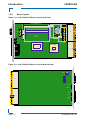
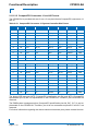
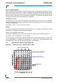
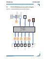
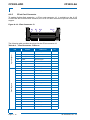
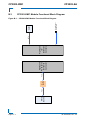
1
CP3003-SA/CP3003-V 3U CompactPCI Processor Board based on the 3rd Generation Intel® Core™ i7 Processor with the Intel® QM77 Chipset Doc. ID: 1052-6929, Rev. 2.0 July 29, 2013 If it’s embedded, it’s Kontron. DRAFT — FOR INTERNAL USE ONLY » User Guide « Preface CP3003-SA/CP3003-V Revision History DRAFT — FOR INTERNAL USE ONLY Publication Title: CP3003-SA/CP3003-V: 3U CompactPCI Processor Board based on the 3 rd Generation Intel® Core™ i7 Processor with the Intel® QM77 Chipset Doc. ID: 1052-6929 Rev. Brief Description of Changes Date of Issue 1.0 Initial issue 14-Nov-2012 2.0 Added description for the CP3003-V 29-Jul-2013 Imprint Kontron Europe GmbH may be contacted via the following: MAILING ADDRESS TELEPHONE AND E-MAIL Kontron Europe GmbH +49 (0) 800-SALESKONTRON Sudetenstraße 7 [email protected] D - 87600 Kaufbeuren Germany For further information about other Kontron products, please visit our Internet web site: www.kontron.com. Disclaimer Copyright © 2013 Kontron AG. All rights reserved. All data is for information purposes only and not guaranteed for legal purposes. Information has been carefully checked and is believed to be accurate; however, no responsibility is assumed for inaccuracies. Kontron and the Kontron logo and all other trademarks or registered trademarks are the property of their respective owners and are recognized. Specifications are subject to change without notice. Page ii ID 1052-6929, Rev. 2.0 CP3003-SA Preface Revision History .........................................................................................................ii Imprint ........................................................................................................................ii Disclaimer ..................................................................................................................ii Table of Contents ...................................................................................................... iii List of Tables .............................................................................................................ix List of Figures ......................................................................................................... xiii Proprietary Note .......................................................................................................xv Trademarks ..............................................................................................................xv Environmental Protection Statement ........................................................................xv Explanation of Symbols .......................................................................................... xvi For Your Safety ...................................................................................................... xvii High Voltage Safety Instructions ........................................................................ xvii Special Handling and Unpacking Instructions ................................................... xvii General Instructions on Usage ............................................................................. xviii Two Year Warranty .................................................................................................. xix 1. Introduction ............................................................................. 1 - 3 1.1 Board Overview ....................................................................................... 1 - 3 1.2 Board-Specific Information ...................................................................... 1 - 3 1.3 System Expansion Capabilities ............................................................... 1 - 5 1.3.1 CP3003-HDD Module (8 HP and 12 HP) ........................................ 1 - 5 1.3.2 CP3003-XMC Module (8 HP) ......................................................... 1 - 5 1.3.3 CP-RIO3-04 Rear I/O Module ......................................................... 1 - 5 1.3.4 SATA Flash Module ........................................................................ 1 - 5 1.3.5 Smart Extension Module ................................................................. 1 - 5 1.4 Board Diagrams ...................................................................................... 1 - 5 1.4.1 Functional Block Diagram ............................................................... 1 - 6 1.4.2 Front Panel ..................................................................................... 1 - 7 1.4.3 Board Layout .................................................................................. 1 - 8 1.5 Technical Specification ............................................................................ 1 - 9 1.6 Standards .............................................................................................. 1 - 14 1.7 Related Publications ............................................................................. 1 - 15 ID 1052-6929, Rev. 2.0 Page iii DRAFT — FOR INTERNAL USE ONLY Table of Contents Preface 2. CP3003-SA Functional Description ............................................................ 2 - 3 2.1 Processor .................................................................................................2 - 3 DRAFT — FOR INTERNAL USE ONLY 2.2 Memory ....................................................................................................2 - 4 2.3 Intel® QM77 Express Chipset .................................................................2 - 5 2.4 Timer ........................................................................................................2 - 5 2.5 Watchdog Timer ......................................................................................2 - 5 2.6 Battery .....................................................................................................2 - 6 2.7 Reset .......................................................................................................2 - 6 2.8 Flash Memory ..........................................................................................2 - 6 2.8.1 SPI Boot Flash for uEFI BIOS .........................................................2 - 6 2.8.2 SATA Flash Module (Optional) ........................................................2 - 7 2.9 8 HP Extension Module ...........................................................................2 - 7 2.10 Trusted Platform Module 1.2 ....................................................................2 - 7 2.11 Board Interfaces ......................................................................................2 - 8 2.11.1 Front Panel LEDs ............................................................................2 - 8 2.11.1.1 Watchdog and Temperature Status LEDs ...............................2 - 8 2.11.1.2 General Purpose LEDs ...........................................................2 - 9 2.11.2 DIP Switch SW1 ............................................................................2 - 10 2.11.3 USB Interfaces ..............................................................................2 - 10 2.11.3.1 Front Panel USB Connectors J5 and J6 ............................... 2 - 11 2.11.4 Integrated Processor Graphics Controller ..................................... 2 - 11 2.11.4.1 Graphics Memory Usage ......................................................2 - 12 2.11.4.2 VGA Analog Interface and Connector J4 ..............................2 - 12 2.11.5 Serial Ports ....................................................................................2 - 12 2.11.6 Gigabit Ethernet ............................................................................2 - 13 2.11.7 SATA Interfaces .............................................................................2 - 14 2.11.7.1 SATA Connector J3 ..............................................................2 - 14 2.11.8 Debug Interface .............................................................................2 - 15 2.11.9 CompactPCI Interface ...................................................................2 - 15 Page iv 2.11.9.1 Board Functionality when Installed in System Controller Slot 2 - 15 2.11.9.2 Board Functionality when Installed in Peripheral Slot ...........2 - 15 2.11.9.3 Front/Rear I/O Configuration ................................................2 - 15 2.11.9.4 Board Insertion/Replacement under Power .........................2 - 16 2.11.9.5 Power Ramping ....................................................................2 - 16 ID 1052-6929, Rev. 2.0 CP3003-SA 2.11.9.6 Preface ENUM# Interrupt .................................................................. 2 - 16 2.11.10 CompactPCI Connectors J1 and J2 ............................................. 2 - 17 2.11.10.2 CompactPCI Connectors J1 and J2 Pinouts ........................ 2 - 18 2.11.10.3 Optional Rear I/O Interface .................................................. 2 - 21 2.11.10.4 Rear I/O Pin Description ...................................................... 2 - 24 3. Installation ............................................................................... 3 - 3 3.1 Safety Requirements ............................................................................... 3 - 3 3.2 Initial Installation Procedures .................................................................. 3 - 4 3.3 Standard Removal Procedures ............................................................... 3 - 5 3.4 Insertion/Removal under Power ............................................................. 3 - 6 3.4.1 Replacement under Power in Peripheral Slot ................................. 3 - 6 3.5 Installation of CP3003-SA Peripheral Devices ........................................ 3 - 8 3.5.1 USB Device Installation ................................................................ 3 - 11 3.5.2 Installation of External SATA Devices ........................................... 3 - 11 3.5.3 SATA Flash Module Installation .................................................... 3 - 11 3.5.4 Smart Extension Module Installation ............................................ 3 - 12 3.5.5 2.5” HDD/SSD Installation ............................................................ 3 - 12 3.5.6 XMC Module Installation ............................................................... 3 - 12 3.5.7 CFast Card Installation ................................................................. 3 - 16 3.5.8 Rear I/O Device Installation .......................................................... 3 - 16 3.5.9 Battery Replacement .................................................................... 3 - 16 3.6 Software Installation .............................................................................. 3 - 17 4. Configuration ........................................................................... 4 - 3 4.1 DIP Switch Configuration ........................................................................ 4 - 3 4.1.1 I/O Address Map ............................................................................. 4 - 4 4.2 CP3003-SA-Specific Registers ............................................................... 4 - 5 4.2.1 Status Register 0 (STAT0) .............................................................. 4 - 5 4.2.2 Status Register 1 (STAT1) .............................................................. 4 - 6 4.2.3 Control Register 0 (CTRL0) ............................................................ 4 - 6 4.2.4 Control Register 1 (CTRL1) ............................................................ 4 - 7 ID 1052-6929, Rev. 2.0 Page v DRAFT — FOR INTERNAL USE ONLY 2.11.10.1 CompactPCI Connector Keying ........................................... 2 - 17 DRAFT — FOR INTERNAL USE ONLY Preface CP3003-SA 4.2.5 Device Protection Register (DPROT) ..............................................4 - 8 4.2.6 Reset Status Register (RSTAT) .......................................................4 - 9 4.2.7 Board Interrupt Configuration Register (BICFG) ...........................4 - 10 4.2.8 Status Register 2 (STAT2) ............................................................. 4 - 11 4.2.9 Board ID High Byte Register (BIDH) ............................................. 4 - 11 4.2.10 Board and PLD Revision Register (BREV) ...................................4 - 12 4.2.11 Geographic Addressing Register (GEOAD) ..................................4 - 12 4.2.12 Board ID Low Byte Register (BIDL) ..............................................4 - 12 4.2.13 Watchdog Timer Control Register (WTIM) ....................................4 - 13 4.2.14 LED Configuration Register (LCFG) .............................................4 - 15 4.2.15 LED Control Register (LCTRL) .....................................................4 - 16 4.2.16 General Purpose Output Register (GPOUT) .................................4 - 17 4.2.17 General Purpose Input Register (GPIN) .......................................4 - 18 5. Power Considerations ............................................................. 5 - 3 5.1 System Power ..........................................................................................5 - 3 5.1.1 CP3003-SA Baseboard ...................................................................5 - 3 5.1.2 Backplane .......................................................................................5 - 4 5.1.3 Power Supply Units .........................................................................5 - 4 5.1.3.1 Start-Up Requirement .............................................................5 - 4 5.1.3.2 Power-Up Sequence ...............................................................5 - 4 5.1.3.3 Tolerance ................................................................................5 - 5 5.1.3.4 Regulation ...............................................................................5 - 5 5.2 Power Consumption ................................................................................5 - 6 5.3 Power Consumption of CP3003-SA Accessories ....................................5 - 8 5.4 Maximum Power Consumption of XMC Modules ....................................5 - 8 6. Thermal Considerations ......................................................... 6 - 3 6.1 Board Internal Thermal Monitoring ..........................................................6 - 3 6.2 Processor Thermal Monitoring .................................................................6 - 3 6.2.1 Digital Thermal Sensor (DTS) .........................................................6 - 3 6.2.2 Adaptive Thermal Monitor ...............................................................6 - 3 6.2.2.1 Page vi Frequency/sVID Control .........................................................6 - 4 ID 1052-6929, Rev. 2.0 CP3003-SA 6.2.2.2 6.2.3 Preface Clock Modulation .................................................................... 6 - 4 Catastrophic Cooling Failure Sensor ............................................. 6 - 4 6.4 External Thermal Regulation ................................................................... 6 - 5 A. 6.4.1 Operational Limits for the CP3003-SA .................................................6 - 6 6.4.2 Peripherals ...................................................................................... 6 - 8 CP3003-HDD Module ...............................................................A - 3 A.1 Overview .................................................................................................A - 3 A.2 Technical Specifications ..........................................................................A - 3 A.3 CP3003-HDD Module Functional Block Diagram ...................................A - 5 A.4 Front Panel of the CP3003-SA with CP3003-HDD Module ....................A - 6 A.5 CP3003-HDD Module Layout ..................................................................A - 7 A.6 Module Interfaces (Front Panel and Onboard) ........................................A - 9 B. A.6.1 DisplayPort Interfaces .....................................................................A - 9 A.6.2 Gigabit Ethernet Interface .............................................................A - 10 A.6.3 USB Interface ............................................................................... A - 11 A.6.4 Serial Port ..................................................................................... A - 11 A.6.5 CFast Card Connector ..................................................................A - 12 A.6.6 SATA Interface ..............................................................................A - 13 A.6.7 Battery ..........................................................................................A - 14 CP3003-XMC Module ...............................................................B - 3 B.1 Overview .................................................................................................B - 3 B.2 Technical Specifications ..........................................................................B - 3 B.3 CP3003-XMC Module Functional Block Diagram ...................................B - 4 B.4 Front Panel of the 8 HP CP3003-SA with CP3003-XMC Module ...........B - 5 B.5 CP3003-XMC Module Layout .................................................................B - 6 B.6 Module Interfaces (Onboard) ..................................................................B - 7 B.6.1 CFast Card Connector ....................................................................B - 7 B.6.2 XMC Connector ..............................................................................B - 8 ID 1052-6929, Rev. 2.0 Page vii DRAFT — FOR INTERNAL USE ONLY 6.3 Chipset Thermal Monitor Feature ............................................................ 6 - 5 Preface C. CP3003-SA CP-RIO3-04 Rear I/O Module ................................................. C - 3 C.1 Overview ................................................................................................. C - 3 DRAFT — FOR INTERNAL USE ONLY C.2 Technical Specifications ......................................................................... C - 3 C.3 Front Panels ........................................................................................... C - 4 C.4 Module Layout: 4 HP and 8 HP Versions ............................................... C - 5 C.5 Module Interfaces ................................................................................... C - 6 D. C.5.1 USB Interfaces ............................................................................... C - 6 C.5.2 VGA Interface ................................................................................. C - 6 C.5.3 Gigabit Ethernet Interface .............................................................. C - 7 C.5.4 COM Interface ................................................................................ C - 8 C.5.5 Peripheral Control Interface ........................................................... C - 9 C.5.6 SATA Interfaces ............................................................................ C - 10 C.5.7 Rear I/O Interface on CompactPCI Connector rJ2 ....................... C - 11 SATA Flash Module ................................................................ D - 3 D.1 Technical Specifications ......................................................................... D - 3 D.2 SATA Flash Module Layout .................................................................... D - 4 E. Smart Extension Module .........................................................E - 3 E.1 Technical Specifications ......................................................................... E - 3 E.2 Smart Extension Module Layout ............................................................. E - 4 E.3 Module Interfaces ................................................................................... E - 5 F. E.3.1 USB Interface ................................................................................. E - 5 E.3.2 SATA Interface ............................................................................... E - 6 CP3003-V ..................................................................................F - 3 F.1 Overview ................................................................................................. F - 3 F.2 CP3003-SA vs. CP3003-V ...................................................................... F - 4 F.3 Processor ................................................................................................ F - 5 F.3.1 Integrated Processor Graphics Controller ...................................... F - 5 F.4 Functional Block Diagram ....................................................................... F - 6 F.5 Front Panel of the CP3003-V .................................................................. F - 7 F.6 Power Consumption ............................................................................... F - 8 F.7 Operational Limits for the CP3003-V .......................................................... F - 10 Page viii ID 1052-6929, Rev. 2.0 CP3003-SA Preface 1-1 CP3003-SA Main Specifications ................................................................ 1 - 9 1-2 Standards ................................................................................................ 1 - 14 1-3 Additional Standards for Boards Ordered with Ruggedized Service ....... 1 - 15 1-4 Related Publications ................................................................................ 1 - 15 2-1 Features of the Processors Supported on the CP3003-SA ....................... 2 - 4 2-2 Watchdog and Temperature Status LEDs Function ................................... 2 - 8 2-3 General Purpose LEDs Function ............................................................... 2 - 9 2-4 POST Code Sequence ............................................................................ 2 - 10 2-5 POST Code Example .............................................................................. 2 - 10 2-6 DIP Switch SW1 Function ....................................................................... 2 - 10 2-7 USB Connectors J5 and J6 Pinout .......................................................... 2 - 11 2-8 Maximum Resolution in 3-Display Configurations ................................... 2 - 11 2-9 D-Sub VGA Connector J4 Pinout ............................................................ 2 - 12 2-10 Pinout of Dual GbE Connector J7A/B ...................................................... 2 - 13 2-11 SATA Connector J3 Pinout ...................................................................... 2 - 14 2-12 CompactPCI Connector J1 System Controller Slot Pinout ...................... 2 - 18 2-13 CompactPCI Connector J1 Peripheral Slot Pinout .................................. 2 - 19 2-14 64-bit CompactPCI Connector J2 Pinout (CP3003-SA Front I/O Vers.) .. 2 - 20 2-15 Rear I/O CompactPCI Connector J2 Pinout (CP3003-SA Rear I/O Vers.) 2 - 22 2-16 Rear I/O Signal Description ..................................................................... 2 - 23 2-17 GPIO Signal Description .......................................................................... 2 - 23 2-18 COMA and COMB Signal Description ..................................................... 2 - 24 2-19 GPIO Signal Description .......................................................................... 2 - 25 2-20 VGA Signal Description ........................................................................... 2 - 25 2-21 Gigabit Ethernet Signal Description ......................................................... 2 - 26 2-22 SATA Signal Description .......................................................................... 2 - 27 2-23 USB Signal Description ........................................................................... 2 - 27 2-24 Power Supply and Power Management Signal Description .................... 2 - 28 4-1 DIP Switch SW1 Functionality ................................................................... 4 - 3 4-2 I/O Address Map ........................................................................................ 4 - 4 4-3 Status Register 0 (STAT0) ......................................................................... 4 - 5 4-4 Status Register 1 (STAT1) ......................................................................... 4 - 6 4-5 Control Register 0 (CTRL0) ....................................................................... 4 - 6 ID 1052-6929, Rev. 2.0 Page ix DRAFT — FOR INTERNAL USE ONLY List of Tables DRAFT — FOR INTERNAL USE ONLY Preface CP3003-SA 4-6 Control Register 1 (CTRL1) ....................................................................... 4 - 7 4-7 Device Protection Register (DPROT) ......................................................... 4 - 8 4-8 Reset Status Register (RSTAT) .................................................................. 4 - 9 4-9 Board Interrupt Configuration Register (BICFG) ...................................... 4 - 10 4-10 Status Register 2 (STAT2) ........................................................................ 4 - 11 4-11 Board ID High Byte Register (BIDH) ........................................................ 4 - 11 4-12 Board and PLD Revision Register (BREV) .............................................. 4 - 12 4-13 Geographic Addressing Register (GEOAD) ............................................. 4 - 12 4-14 Board ID Low Byte Register (BIDL) ......................................................... 4 - 12 4-15 Watchdog Timer Control Register (WTIM) ............................................... 4 - 14 4-16 LED Configuration Register (LCFG) ........................................................ 4 - 15 4-17 LED Control Register (LCTRL) ................................................................ 4 - 16 4-18 General Purpose Output Register (GPOUT) ............................................ 4 - 17 4-19 General Purpose Input Register (GPIN) .................................................. 4 - 18 5-1 Maximum Input Power Voltage Limits ........................................................ 5 - 3 5-2 DC Operational Input Voltage Ranges ....................................................... 5 - 3 5-3 Input Voltage Characteristics ..................................................................... 5 - 5 5-4 CP3003-SA in EFI Shell ............................................................................. 5 - 7 5-5 CP3003-SA with Win. 7 and Processor and Graphics in Idle State ........... 5 - 7 5-6 CP3003-SA with Win. 7 and Max. Proc. Workload and Basic Graph. Oper. 5 - 7 5-7 CP3003-SA with Win. 7 and Max. Processor and Graphics Workload ...... 5 - 7 5-8 Power Consumption of CP3003-SA Accessories ...................................... 5 - 8 5-9 XMC Module Current ................................................................................. 5 - 8 A-1 CP3003-HDD Module Specifications ........................................................ A - 3 A-2 DisplayPort Connectors J1 and J2 Pinout ................................................. A - 9 A-3 Gigabit Ethernet Connector J5 Pinout ..................................................... A - 10 A-4 USB Connector J7 Pinout ........................................................................ A - 11 A-5 Serial Port Connector J8 Pinout ............................................................... A - 11 A-6 CFast Connector J3 Pinout ..................................................................... A - 12 A-7 SATA Connector J6/J2 Pinout ................................................................. A - 13 B-1 CP3003-XMC Module Specifications ........................................................ B - 3 B-2 CFast Connector J2 Pinout ....................................................................... B - 7 B-3 XMC Connector J1 Pinout ......................................................................... B - 8 C-1 CP-RIO3-04 Rear I/O Module Main Specifications ................................... C - 3 Page x ID 1052-6929, Rev. 2.0 CP3003-SA Preface C-2 USB Con. J11 and J12 Pinout ................................................................... C - 6 C-3 D-Sub VGA Connector J7 Pinout .............................................................. C - 6 C-5 COM Connectors J2a (COMA) and J3a (COMB) Pinout ........................... C - 8 C-6 Serial Port Con. J2 (COMA) and J3 (COMB) Pinout ................................. C - 9 C-7 Peripheral Connector J13 Pinout ............................................................... C - 9 C-8 SATA Connectors J5 and J6 Pinout ......................................................... C - 10 C-9 Rear I/O CompactPCI Connector rJ2 Pinout ........................................... C - 12 C-10 Rear I/O Signal Description ..................................................................... C - 13 D-1 SATA Flash Module Specifications ............................................................ D - 3 E-1 Smart Extension Module Specifications .................................................... E - 3 E-2 USB Connector J2 Pinout .......................................................................... E - 5 E-3 SATA Connector J1 Pinout ........................................................................ E - 6 F-1 CP3003-SA vs. CP3003-V ........................................................................ F - 4 F-2 Features of the Intel® Celeron® 807UE Processor ................................... F - 5 F-3 Maximum Resolution in 3-Display Configurations ..................................... F - 5 F-4 CP3003-V in EFI Shell ............................................................................... F - 9 F-5 CP3003-V with Win. 7 and Processor and Graphics in Idle State ............. F - 9 F-6 CP3003-V with Win. 7 and Max. Proc. Workload and Basic Graph. Oper. F - 9 F-7 CP3003-V with Win. 7 and Max. Processor and Graphics Workload ........ F - 9 ID 1052-6929, Rev. 2.0 Page xi DRAFT — FOR INTERNAL USE ONLY C-4 Dual Gigabit Ethernet Connector J10A/B Pinout ....................................... C - 7 DRAFT — FOR INTERNAL USE ONLY Preface CP3003-SA This page has been intentionally left blank. Page xii ID 1052-6929, Rev. 2.0 CP3003-SA Preface 1-1 CP3003-SA Functional Block Diagram .................................................... 1 - 6 1-2 4 HP CP3003-SA Front Panel ................................................................. 1 - 7 1-3 4 HP CP3003-SA Board Layout (Top View) ............................................. 1 - 8 1-4 4 HP CP3003-SA Board Layout (Bottom View) ....................................... 1 - 8 2-1 USB Connectors J5 and J6 .................................................................... 2 - 11 2-2 D-Sub VGA Connector J4 ...................................................................... 2 - 12 2-3 Dual Gigabit Ethernet Connector J7A/B ................................................ 2 - 13 2-4 SATA Connector J3 ................................................................................ 2 - 14 2-5 CPCI Connectors J1/J2 ......................................................................... 2 - 17 3-1 4 HP CP3003-SA with SATA Flash Module ............................................. 3 - 8 3-2 4 HP CP3003-SA with Smart Extension Module ..................................... 3 - 9 3-3 8 HP CP3003-SA with CP3003-HDD Module .......................................... 3 - 9 3-4 12 HP CP3003-SA with CP3003-HDD Module and SATA Adapter Mod. 3 - 10 3-5 8 HP CP3003-SA with CP3003-XMC Module ........................................ 3 - 10 3-6 Screws Securing the Front Panel and the CP3003-XMC to the CP3003-SA . 3 - 13 3-7 Screws Securing the XMC Module to the CP3003-XMC Ext. Module ... 3 - 13 3-8 CP3003-SA Board with CP3003-XMC Ext. Module and XMC Module .. 3 - 14 3-9 CP3003-SA with Front Panel, CP3003-XMC Ext. Module and XMC Mod. ... 3 - 14 4-1 DIP Switch SW1 ....................................................................................... 4 - 3 6-1 CP3003-SA with i7-3612QE (SV), 2.1 GHz ............................................. 6 - 6 6-2 CP3003-SA with i7-3555LE (LV), 2.5 GHz .............................................. 6 - 7 6-3 CP3003-SA with i7-3517UE (ULV), 1.7 GHz ........................................... 6 - 7 A-1 CP3003-HDD Module Functional Block Diagram .................................... A - 5 A-2 Front Panel of the 8 HP and 12 HP CP3003-SA with CP3003-HDD Mod. A - 6 A-3 CP3003-HDD Module Layout for 8 HP Board Version (Top View) ........... A - 7 A-4 CP3003-HDD Module Layout for 12 HP Board Version (Top View) ......... A - 7 A-5 SATA Adapter for 2.5" SATA HDD/SSD (Top View) ................................. A - 8 A-6 DisplayPort Connectors J1 and J2 ........................................................... A - 9 A-7 Gigabit Ethernet Connector J5 ............................................................... A - 10 A-8 USB Connector J7 ................................................................................. A - 11 A-9 Serial Port Connector J8 ........................................................................ A - 11 A-10 CFast Connector J3 ............................................................................... A - 12 A-11 SATA Connector J6/J2 ........................................................................... A - 13 ID 1052-6929, Rev. 2.0 Page xiii DRAFT — FOR INTERNAL USE ONLY List of Figures DRAFT — FOR INTERNAL USE ONLY Preface CP3003-SA B-1 CP3003-XMC Module Functional Block Diagram ................................... B - 4 B-2 Front Panel of the 8 HP CP3003-SA with CP3003-XMC Module ........... B - 5 B-3 CP3003-XMC Module Layout (Top View) ................................................ B - 6 B-4 CP3003-XMC Module Layout (Bottom View) .......................................... B - 6 B-5 CFast Connector J6 ................................................................................ B - 7 B-6 XMC Connector J1 .................................................................................. B - 8 C-1 CP-RIO3-04 Front Panels, 4 HP and 8 HP Versions .............................. C - 4 C-2 CP-RIO3-04 Rear I/O Module Layout, 4 HP Version .............................. C - 5 C-3 CP-RIO3-04 Rear I/O Module Layout, 8 HP Version ............................. C - 5 C-4 USB Connectors J11/J12 ........................................................................ C - 6 C-5 D-Sub VGA Connector J7 ....................................................................... C - 6 C-6 Dual Gigabit Ethernet Connector J10A/B ................................................ C - 7 C-7 COM Connectors J2a (COMA) and J3a (COMB) .................................... C - 8 C-8 Serial Port Connectors J2 (COMA) and J3 (COMB) ............................... C - 9 C-9 Peripheral Connector J13 ........................................................................ C - 9 C-10 SATA Connectors J5 and J6 .................................................................. C - 10 C-11 Rear I/O CompactPCI Connector rJ2 .................................................... C - 11 D-1 SATA Flash Module Layout (Top View) ................................................... D - 4 D-2 SATA Flash Module Layout (Bottom View) .............................................. D - 4 E-1 Smart Extension Module Layout (Top View) ........................................... E - 4 E-2 Smart Extension Module Layout (Bottom View) ...................................... E - 4 E-3 USB Connector J2 ................................................................................... E - 5 E-4 SATA Connector J1 ................................................................................. E - 6 F-1 CP3003-V Functional Block Diagram ...................................................... F - 6 F-2 Front Panel of the CP3003-V .................................................................. F - 7 F-3 CP3003-V with Celeron® 807UE, 1.0 GHz ........................................... F - 10 Page xiv ID 1052-6929, Rev. 2.0 CP3003-SA Preface This document contains information proprietary to Kontron. It may not be copied or transmitted by any means, disclosed to others, or stored in any retrieval system or media without the prior written consent of Kontron or one of its authorized agents. The information contained in this document is, to the best of our knowledge, entirely correct. However, Kontron cannot accept liability for any inaccuracies or the consequences thereof, or for any liability arising from the use or application of any circuit, product, or example shown in this document. Kontron reserves the right to change, modify, or improve this document or the product described herein, as seen fit by Kontron without further notice. Trademarks Kontron, the PEP logo and, if occurring in this manual, “CXM” are trademarks owned by Kontron, Kaufbeuren (Germany). In addition, this document may include names, company logos and trademarks, which are registered trademarks and, therefore, proprietary to their respective owners. Environmental Protection Statement This product has been manufactured to satisfy environmental protection requirements where possible. Many of the components used (structural parts, printed circuit boards, connectors, batteries, etc.) are capable of being recycled. Final disposition of this product after its service life must be accomplished in accordance with applicable country, state, or local laws or regulations. ID 1052-6929, Rev. 2.0 Page xv DRAFT — FOR INTERNAL USE ONLY Proprietary Note Preface CP3003-SA Explanation of Symbols Caution, Electric Shock! DRAFT — FOR INTERNAL USE ONLY This symbol and title warn of hazards due to electrical shocks (> 60V) when touching products or parts of them. Failure to observe the precautions indicated and/or prescribed by the law may endanger your life/health and/or result in damage to your material. Please refer also to the section “High Voltage Safety Instructions” on the following page. Warning, ESD Sensitive Device! This symbol and title inform that electronic boards and their components are sensitive to static electricity. Therefore, care must be taken during all handling operations and inspections of this product, in order to ensure product integrity at all times. Please read also the section “Special Handling and Unpacking Instructions” on the following page. Warning! This symbol and title emphasize points which, if not fully understood and taken into consideration by the reader, may endanger your health and/or result in damage to your material. Note ... This symbol and title emphasize aspects the reader should read through carefully for his or her own advantage. Page xvi ID 1052-6929, Rev. 2.0 CP3003-SA Preface Your new Kontron product was developed and tested carefully to provide all features necessary to ensure its compliance with electrical safety requirements. It was also designed for a long fault-free life. However, the life expectancy of your product can be drastically reduced by improper treatment during unpacking and installation. Therefore, in the interest of your own safety and of the correct operation of your new Kontron product, you are requested to conform with the following guidelines. High Voltage Safety Instructions Warning! All operations on this device must be carried out by sufficiently skilled personnel only. Caution, Electric Shock! Before installing a not hot-swappable Kontron product into a system always ensure that your mains power is switched off. This applies also to the installation of piggybacks. Serious electrical shock hazards can exist during all installation, repair and maintenance operations with this product. Therefore, always unplug the power cable and any other cables which provide external voltages before performing work. Special Handling and Unpacking Instructions ESD Sensitive Device! Electronic boards and their components are sensitive to static electricity. Therefore, care must be taken during all handling operations and inspections of this product, in order to ensure product integrity at all times. Do not handle this product out of its protective enclosure while it is not used for operational purposes unless it is otherwise protected. Whenever possible, unpack or pack this product only at EOS/ESD safe work stations. Where a safe work station is not guaranteed, it is important for the user to be electrically discharged before touching the product with his/her hands or tools. This is most easily done by touching a metal part of your system housing. It is particularly important to observe standard anti-static precautions when changing piggybacks, ROM devices, jumper settings etc. If the product contains batteries for RTC or memory backup, ensure that the board is not placed on conductive surfaces, including anti-static plastics or sponges. They can cause short circuits and damage the batteries or conductive circuits on the board. ID 1052-6929, Rev. 2.0 Page xvii DRAFT — FOR INTERNAL USE ONLY For Your Safety Preface CP3003-SA DRAFT — FOR INTERNAL USE ONLY General Instructions on Usage In order to maintain Kontron’s product warranty, this product must not be altered or modified in any way. Changes or modifications to the device, which are not explicitly approved by Kontron and described in this manual or received from Kontron’s Technical Support as a special handling instruction, will void your warranty. This device should only be installed in or connected to systems that fulfill all necessary technical and specific environmental requirements. This applies also to the operational temperature range of the specific board version, which must not be exceeded. If batteries are present, their temperature restrictions must be taken into account. In performing all necessary installation and application operations, please follow only the instructions supplied by the present manual. Keep all the original packaging material for future storage or warranty shipments. If it is necessary to store or ship the board, please re-pack it as nearly as possible in the manner in which it was delivered. Special care is necessary when handling or unpacking the product. Please consult the special handling and unpacking instruction on the previous page of this manual. Page xviii ID 1052-6929, Rev. 2.0 CP3003-SA Preface Kontron grants the original purchaser of Kontron’s products a TWO YEAR LIMITED HARDWARE WARRANTY as described in the following. However, no other warranties that may be granted or implied by anyone on behalf of Kontron are valid unless the consumer has the express written consent of Kontron. Kontron warrants their own products, excluding software, to be free from manufacturing and material defects for a period of 24 consecutive months from the date of purchase. This warranty is not transferable nor extendible to cover any other users or long-term storage of the product. It does not cover products which have been modified, altered or repaired by any other party than Kontron or their authorized agents. Furthermore, any product which has been, or is suspected of being damaged as a result of negligence, improper use, incorrect handling, servicing or maintenance, or which has been damaged as a result of excessive current/voltage or temperature, or which has had its serial number(s), any other markings or parts thereof altered, defaced or removed will also be excluded from this warranty. If the customer’s eligibility for warranty has not been voided, in the event of any claim, he may return the product at the earliest possible convenience to the original place of purchase, together with a copy of the original document of purchase, a full description of the application the product is used on and a description of the defect. Pack the product in such a way as to ensure safe transportation (see our safety instructions). Kontron provides for repair or replacement of any part, assembly or sub-assembly at their own discretion, or to refund the original cost of purchase, if appropriate. In the event of repair, refunding or replacement of any part, the ownership of the removed or replaced parts reverts to Kontron, and the remaining part of the original guarantee, or any new guarantee to cover the repaired or replaced items, will be transferred to cover the new or repaired items. Any extensions to the original guarantee are considered gestures of goodwill, and will be defined in the “Repair Report” issued by Kontron with the repaired or replaced item. Kontron will not accept liability for any further claims resulting directly or indirectly from any warranty claim, other than the above specified repair, replacement or refunding. In particular, all claims for damage to any system or process in which the product was employed, or any loss incurred as a result of the product not functioning at any given time, are excluded. The extent of Kontron liability to the customer shall not exceed the original purchase price of the item for which the claim exists. Kontron issues no warranty or representation, either explicit or implicit, with respect to its products’ reliability, fitness, quality, marketability or ability to fulfil any particular application or purpose. As a result, the products are sold “as is,” and the responsibility to ensure their suitability for any given task remains that of the purchaser. In no event will Kontron be liable for direct, indirect or consequential damages resulting from the use of our hardware or software products, or documentation, even if Kontron were advised of the possibility of such claims prior to the purchase of the product or during any period since the date of its purchase. Please remember that no Kontron employee, dealer or agent is authorized to make any modification or addition to the above specified terms, either verbally or in any other form, written or electronically transmitted, without the company’s consent. ID 1052-6929, Rev. 2.0 Page xix DRAFT — FOR INTERNAL USE ONLY Two Year Warranty DRAFT — FOR INTERNAL USE ONLY Preface CP3003-SA This page has been intentionally left blank. Page xx ID 1052-6929, Rev. 2.0 Introduction Chapter 1 Introduction ID 1052-6929, Rev. 2.0 Page 1 - 1 DRAFT — FOR INTERNAL USE ONLY CP3003-SA DRAFT — FOR INTERNAL USE ONLY Introduction CP3003-SA This page has been intentionally left blank. Page 1 - 2 ID 1052-6929, Rev. 2.0 1. Introduction 1.1 Board Overview Introduction The CP3003-SA is a highly integrated 3U, 4 HP CompactPCI system controller board optionally expandable to 8 HP and available either as a front I/O version or as a rear I/O version. It has been designed to support the multi-chip package, 3rd generation Intel® Core™ i7 processor combined with the mobile Intel® QM77 Express Chipset. The board supports the Intel® Core™ i7-3612QE quad-core processor with 2.1 GHz frequency, the Intel® Core™ i7-3555LE dual-core processor with 2.5 GHz frequency and the Intel® Core™ i7-3517UE dual-core processor with 1.7 GHz frequency. All processors are built on 22nm technology and provided in a BGA package. The processor is soldered on the CP3003-SA, which results in a higher Mean Time Between Failures (MTBF) and a significant improvement in cooling. Two SODIMM sockets are available on the CP3003-SA to provide up to 16 GB dual-channel, DDR3 memory with Error Checking and Correction (ECC) running at 1600 MHz. The graphics controller and the memory controller are integrated in the processor. Furthermore, an external HDD/SSD and either a SATA Flash module with up to 32 GB SLC NAND flash memory or a Smart Extension Module (a SATA/USB 2.0 adapter) can be integrated onto the CP3003-SA. The CP3003-SA comes with three Gigabit Ethernet ports, one VGA interface, two COM ports, six SATA interfaces, four USB 2.0 ports, one USB 3.0 port, two DisplayPort interfaces, and one x8 PCI Express 2.0 XMC interface. The CP3003-SA provides support for one 8 HP I/O extension module such as the CP3003-HDD or the CP3003-XMC as well as one rear I/O module such as the CP-RIO3-04. The board supports a configurable 32-bit/ 33 MHz (66 MHz on request) PCI/PCI-X hot swap CompactPCI interface. When installed in the system slot, the interface is enabled, and when installed in a peripheral slot, the CP3003-SA is isolated from the CompactPCI bus. The CP3003-SA further provides safety and security features via a Trusted Platform Module (TPM) 1.2. The board fits into all applications situated in industrial environments, including I/O intensive applications where only one slot is available for the CPU, making it a perfect core technology for long-life applications. Components which have high temperature tolerance have been selected from embedded technology programs, and therefore offer long-term availability. The board is offered with various Board Support Packages including Windows, VxWorks and Linux operating systems. For further information concerning the operating systems available for the CP3003-SA, please contact Kontron. 1.2 Board-Specific Information The CP3003-SA is a CompactPCI single-board computer based on the 3rd generation Intel® Core™ i7 processor and specifically designed for use in highly integrated platforms with solid mechanical interfacing for a wide range of industrial environment applications. ID 1052-6929, Rev. 2.0 Page 1 - 3 DRAFT — FOR INTERNAL USE ONLY CP3003-SA DRAFT — FOR INTERNAL USE ONLY Introduction CP3003-SA Some of the CP3003-SA's outstanding features include: • Support for the following 3rd generation processors: • Intel® Core™ i7-3612QE (SV) quad-core processor, 2.1 GHz, 6 MB L3 cache • Intel® Core™ i7-3555LE (LV) dual-core processor, 2.5 GHz, 4 MB L3 cache • Intel® Core™ i7-3517UE (ULV) dual-core processor, 1.7 GHz, 4 MB L3 cache • Intel® QM77 Express Chipset • Up to 16 GB, dual-channel, DDR3 SDRAM memory with ECC running at 1600 MHz on two SODIMM sockets • Integrated 3D high-performance processor graphics controller with up to three high-resolution graphics interfaces (1x VGA and 2 x DP) • Digital display support for resolutions up to 2560 x 1600 pixels @ 60 Hz • Analog display support for resolutions up to 2048 x 1536 pixels @ 75 Hz • Three Gigabit Ethernet interfaces based on three Intel® 82574L controllers: • Two interfaces switchable between front I/O and rear I/O (with Wake-on-LAN support) • One interface available on the CP3003-HDD extension module (8HP) • Six SATA interfaces with SATA RAID 0/1/5/10 support: • One SATA 6 Gb/s interface for one external, standard HDD/SSD • One SATA 3 Gb/s interface for up to 32 GB SLC NAND flash memory via an optional SATA Flash module • One SATA 3 Gb/s interface for one CFast memory card (8 HP with CP3003-HDD/ CP3003-XMC) or one SATA 2.5" HDD/SSD (12 HP) • One SATA 6 Gb/s interface for one SATA 2.5" HDD/SSD (8 HP with CP3003-HDD) • Two SATA 3 Gb/s interfaces for rear I/O • Five USB ports: • Two USB 2.0 ports on front I/O • Two USB 2.0 ports on rear I/O • One USB 3.0 port on the 120-pin onboard high-speed I/O extension connector • Two DisplayPort interfaces available on the CP3003-HDD extension module • One x8 PCI Express 2.0 XMC interface available on the CP3003-XMC ex. module • 32-bit/ 33 MHz PCI/PCI-X hot swap CompactPCI interface (PICMG 2.0); 66 MHz on request • Compatible with CompactPCI Specification PICMG 2.0 Rev. 3.0 and usable in the system controller slot as well as in a peripheral slot (the PCI interface is isolated in peripheral slot) • TCG 1.2-compliant Trusted Platform Module (TPM) • Two SPI boot flashes for two separate uEFI BIOS images: • One standard SPI boot flash • One recovery SPI boot flash • Watchdog timer • Battery-backed real-time clock (RTC) • One onboard DIP switch for board configuration • Two COM ports: • COMA (RS-232) either on the 8 HP extension module or on the rear I/O • COMB (RS-232) on the rear I/O • Peripheral extension connectors: • 120-pin high-speed I/O extension connector for 8 HP extension • 60-pin high-speed PCI Express extension connector for 8 HP extension • SPI extension connector • Rear I/O on the CompactPCI connector J2 • 4 HP or 8 HP, 3U CompactPCI (12 HP on request) • Several rear I/O configurations • Power-up sequencing and in-rush current optimized design • Passive heat sink solution for forced airflow cooling • AMI Aptio®, a uEFI-compliant platform firmware Page 1 - 4 ID 1052-6929, Rev. 2.0 1.3 System Expansion Capabilities 1.3.1 CP3003-HDD Module (8 HP and 12 HP) Introduction The CP3003-HDD module for the 8 HP CP3003-SA version provides various I/O ports. On the front panel, it includes two DisplayPort connectors, one Gigabit Ethernet port, one USB 3.0 port, and one RS-232 COM port. Onboard ports include one SATA connector for SATA 2.5” HDD or SSD devices as well as a CFast card socket. As a further extension capability of the CP3003-SA to 12 HP, a SATA adapter module is available for use in conjunction with the CP3003-HDD module to provide an additional SATA connector for a 2.5" SATA HDD/SSD device. The 12 HP CP3003-SA does not provide a CFast card socket. For further information concerning the CP3003-HDD module, refer to Appendix A. 1.3.2 CP3003-XMC Module (8 HP) The CP3003-XMC module for the 8 HP CP3003-SA version provides one XMC mezzanine interface for support of one x8, x4 or x1 PCI Express 2.0 XMC module. In addition, the CP3003XMC module provides a socket for CFast memory cards. For further information concerning the CP3003-XMC module, refer to Appendix B. 1.3.3 CP-RIO3-04 Rear I/O Module The CP-RIO3-04 rear I/O module has been designed for use with the CP3003-SA board from Kontron and provides comprehensive rear I/O functionality. For further information concerning the CP-RIO3-04 rear I/O module, refer to Appendix C. 1.3.4 SATA Flash Module The 4 HP CP3003-SA provides support for up to 32 GB of SLC NAND flash memory in combination with an optional SATA Flash module, which is connected to an onboard connector. For further information concerning the SATA Flash module, refer to Appendix D. 1.3.5 Smart Extension Module The Smart Extension Module expands the onboard I/O capability and provides one additional SATA cable connector as well as one USB 2.0 connector thereby facilitating the connection to system-internal USB and SATA devices. For further information concerning the SATA Flash module, refer to Appendix E. 1.4 Board Diagrams The following diagrams provide additional information concerning board functionality and component layout. ID 1052-6929, Rev. 2.0 Page 1 - 5 DRAFT — FOR INTERNAL USE ONLY CP3003-SA Page 1 - 6 USB 2.0 Type A USB 2.0 Type A USB USB Watchdog / Thermal LEDs POST Code / Debug / Gen. Purpose LEDs DSUB 15-pin RJ-45 GbE VGA CRT RJ-45 LPC COMA+B XBUS COMA To Rear I/O CPLD VGA Mux GbE Contr. GbE Switch Rear I/O Eth GbE Contr. GbE Switch Rear I/O Eth Dual UART PCIe x8 Debug TPM HighSpeed I/O Extension Connector VGA CRT 2x USB 2.0 PCIe x1 PCIe x1 HighSpeed PCIe Extension Connector SFF XDP Intel® QM77 FDI FDI SPI Boot Flashes (standard/ recovery) LPC SPI EEPROM SMBus SATA, PCIe, HDA, USB 3.0 DP DMI DMI Bat. SATA RTC USB SATA PCIe DDR3 PCIe x1 USB Power (optional) SATA 6 Gb/s PCI Power Management COMA + COMB or COMA + GPIO SATA Flash Module SATA 7-pin Connector VGA CRT 2x USB 2.0 2x SATA 3 Gb/s PCI Bridge Rear I/O Eth Rear I/O Eth Onboard Power Supplies DC/DC etc. 2x SATA DDR3 / DDR3L w ECC Bank B SODIMM 3rd gen. Intel® Core™ i7 VGA CRT USB PCIe PCIe PCIe DDR3 DDR3 / DDR3L w ECC Bank A SODIMM 3.3V and 5V PM COMA & COMB (TTL) 2x USB Power VGA 2x USB 2.0 2x SATA 3 Gb/s PCI 32-bit / 33MHz 3.3V / 5V VIO GbE GbE CompactPCI Connector 1.4.1 GbE Front Panel DRAFT — FOR INTERNAL USE ONLY Introduction CP3003-SA Functional Block Diagram Figure 1-1: CP3003-SA Functional Block Diagram ID 1052-6929, Rev. 2.0 CP3003-SA 1.4.2 Introduction Front Panel Watchdog and Overtemperature Status LEDs CP3003 WD (green): TH (red/green): Watchdog Status Overtemperature Status Integral Ethernet LEDs ACT (green): SPEED (green/orange/off): Ethernet Link/Activity Ethernet Speed General Purpose LEDs LED0..3 (red/green/red+green): General Purpose/POST Code Note ... USB 2.0 If the General Purpose LEDs 0..3 are lit red during boot-up, a failure is indicated before the uEFI BIOS has started. GbE A GbE B Note ... For information regarding the front panel of the 8 HP or 12 HP CP3003-SA with a CP3003-HDD module, refer to Appendix A, CP3003-HDD Module. For information regarding the front panel of the 8 HP CP3003-SA with a CP3003-XMC module, refer to Appendix B, CP3003-XMC Module. ID 1052-6929, Rev. 2.0 Page 1 - 7 DRAFT — FOR INTERNAL USE ONLY Figure 1-2: 4 HP CP3003-SA Front Panel Introduction 1.4.3 CP3003-SA Board Layout DRAFT — FOR INTERNAL USE ONLY Figure 1-3: 4 HP CP3003-SA Board Layout (Top View) DDR3 SODIMM Sockets Ch. A 1 2 J11 9 10 1 J3 Ch. B J4 VGA J2 J8 J14 J12 Memory Modules 1 2 1 2 SATA Flash Module J5 USB J6 USB 17 18 13 14 J13 Smart Extension Module Intel® Core™i7 Intel® QM77 J7A GbE A Processor J7B GbE B J1 Chipset Figure 1-4: 4 HP CP3003-SA Board Layout (Bottom View) SW1 ON J2 J15 TH LED WD LED LED 0 LED 1 J1 LED 2 LED 3 Page 1 - 8 ID 1052-6929, Rev. 2.0 CP3003-SA Technical Specification Table 1-1: CP3003-SA Main Specifications FEATURES The CP3003-SA supports the following 3 rd generation microprocessors: • Quad-core Intel® Core™ i7-3612QE (SV), 2.1 GHz, 6 MB L3 cache • Dual-core Intel® Core™ i7-3555LE (LV), 2.5 GHz, 4 MB L3 cache • Dual-core Intel® Core™ i7-3517UE (ULV), 1.7 GHz, 4 MB L3 cache Further processor features used on the CP3003-SA: • Up to four execution cores • Intel® Hyper-Threading Technology (Intel® HT Technology) • Intel® 64 Architecture • Intel® Advanced Vector Extensions (AVX) floating point • Intel® Turbo Boost Technology • System memory interface with optimized support for dual-channel DDR3 SDRAM memory at 1600 MHz with ECC • Integrated 2D and 3D Graphics Engines • DMI 2.0 with 5 GT/s and FDI interfaces to the Intel® QM77 Chipset • One x8 PCI Express 2.0 port operating at 5 GT/s Please contact Kontron for further information concerning the suitability of other Intel processors for use with the CP3003-SA. Memory Main Memory: • Up to 16 GB, dual-channel DDR3 SDRAM memory with ECC running at 1600 MHz on two SODIMM sockets Cache Structure: • 64 kB L1 cache for each core • 32 kB instruction cache • 32 kB data cache • 256 kB L2 shared instruction/data cache for each core • Up to 6 MB L3 shared instruction/data cache shared between all cores Flash Memory: • Two SPI boot flash chips (2 x 8 MB) for two separate uEFI BIOS images • Up to 32 GB SLC NAND flash via an onboard SATA Flash module (SSD) Serial EEPROM with 64 kbit Intel® QM77 Mobile Intel® QM77 Express Chipset features used on the CP3003-SA: • Four x1 PCI Express 2.0 ports operating at 5 GT/s • SATA host controller with six ports and RAID 0/1/5/10 support • Two SATA 6 Gb/s ports • Four SATA 3 Gb/s ports • Four USB 2.0 host interfaces and up to two USB 3.0 host interfaces • Integrated Ethernet controller • SPI flash interface support • Low Pin Count (LPC) interface • Power management logic support • Enhanced DMA controller, interrupt controller, and timer functions • System Management Bus (SMBus) compatible with most I²C™ devices • DMI 2.0 with 5 GT/s and FDI interfaces to the processor • Analog display port • Two digital display ports • High Definition Audio interface • Integrated RTC Chipset Processor and Memory CPU SPECIFICATIONS ID 1052-6929, Rev. 2.0 Page 1 - 9 DRAFT — FOR INTERNAL USE ONLY 1.5 Introduction Introduction Table 1-1: CP3003-SA CP3003-SA Main Specifications (Continued) SPECIFICATIONS High-performance 3D graphics controller integrated in the processor: • Dynamic Video Memory Technology (DVMT) • Supports digital displays with resolutions up to 2560 x 1600 pixels @ 60 Hz through DisplayPort or up to 1920x1200 pixels @ 60Hz using HDMI/DVI. HDMI/DVI displays are supported via an appropriate adapter. Refer to Chapter 2.11.4, Table 2-8 for further information on the display configuration options. • Supports analog display with resolutions up to 2048 x 1536 pixels @ 75 Hz for VGA displays CompactPCI Compliant with CompactPCI Specification PICMG® 2.0 R 3.0: Integrated Controller Graphics Controller • • • • System master operation 32-bit / 33 MHz master interface (66 MHz on request) 3.3 V or 5 V (universal PCI interface) Support for up to seven peripheral slots (7x REQ/GNT signals) When installed in a peripheral slot, the CP3003-SA is isolated from the CompactPCI bus. It receives power from the backplane and supports rear I/O. CP3003-SA removal under power: When installed in a peripheral slot, the CP3003-SA supports hot plugging on the power interface through a dedicated power controller, but not on the PCI interface. Hot swapping of peripheral boards controlled by the CP3003-SA: Interfaces DRAFT — FOR INTERNAL USE ONLY FEATURES When installed in the system controller slot, the CP3003-SA supports the hot swapping of other boards. Individual clocks for each slot and Enum signal handling are in compliance with the PICMG 2.1 Hot Swap Specification. The CP3003-SA itself, however, is not hot swappable. When installed in the system controller slot, the system must be powered down in order to replace the board. Rear I/O The following interfaces are routed to the rear I/O connector J2: • COMA and COMB, or COMA and GPIO (all ports have 3.3V LVTTL sig• • • • • • • Page 1 - 10 naling) 2 x USB 2.0 VGA (analog) 2x Gigabit Ethernet 2x SATA 3Gb/s System management signals Input for 5V standby power General purpose signals ID 1052-6929, Rev. 2.0 CP3003-SA CP3003-SA Main Specifications (Continued) FEATURES Gigabit Ethernet SPECIFICATIONS Three 10 Base-T/100 Base-TX/1000 Base-T Gigabit Ethernet interfaces based on three Intel® 82574L Ethernet PCI Express bus controllers, two interfaces individually switchable to front I/O or rear I/O, one interface available on the CP3003-HDD module: • • • • USB Dual RJ-45 connector on the front panel Automatic mode recognition (Auto-Negotiation) Automatic cabling configuration recognition (Auto-MDI/X) Wake-on-LAN support available only on the two interfaces switchable to front I/O or rear I/O Five USB ports: • Two USB 2.0 ports on the front I/O • Two USB 2.0 ports on the rear I/O interface • One USB 3.0 port on the 120-pin onboard high-speed I/O extension connector Serial SATA Two 16C550-compatible UARTs: • COMA available on the 8 HP extension module or on rear I/O • COMB or GPIO available on rear I/O only • Six SATA ports, two onboard, two on rear I/O, and two on the 8 HP ex- Interfaces tension module • Data transfer rates up to 600 MB/s • High-performance RAID 0/1/5/10 functionality on all SATA ports I/O Expansion Interfaces I/O expansion to 8 HP board version via the CP3003-HDD module: • SATA 6 Gb/s • CFast (SATA 3 Gb/s) • USB 3.0 • 2x DP (DisplayPort) • COMA • Reset button and HDD/SSD activity LED • Gigabit Ethernet I/O expansion to 12 HP board version via the CP3003-HDD module and the 2.5" SATA adapter module: • 2x SATA (SATA 3 Gb/s and SATA 6 Gb/s) • USB 3.0 • 2x DP (DisplayPort) • COMA • Reset button and HDD/SSD activity LED • Gigabit Ethernet I/O expansion to 8 HP board version via the CP3003-XMC module: • PCI Express x8, x4 or x1 • CFast (SATA 3 Gb/s) I/O expansion of CP3003-SA via the Smart Extension Module (exceeds 4 HP): • SATA 3 Gb/s • USB 2.0 ID 1052-6929, Rev. 2.0 Page 1 - 11 DRAFT — FOR INTERNAL USE ONLY Table 1-1: Introduction Introduction Table 1-1: CP3003-SA CP3003-SA Main Specifications (Continued) Front Panel Connectors • VGA: 15-pin D-Sub connector, J4 • USB: two 4-pin, type A connectors, J5 and J6 • Ethernet: dual RJ-45 connector, J7A/B Onboard Connectors • • • • • • • • • Sockets Switch SPECIFICATIONS 7-pin, L-form standard SATA connector, J3 120-pin, high-speed I/O extension connector, J14 60-pin, high-speed PCI Express extension connector, J8 SPI extension connector, J11 18-pin extension connector for the SATA Flash module (SSD), J12 JTAG connector, J13 XDP-SFF (debug) connector, J15 CompactPCI connectors J1 and J2 Two 204-pin DDR3 SODIMM sockets DIP Switch One DIP switch, SW1, for board configuration LEDs Watchdog and Overtemperature Status LEDs: • WD (green): • TH (red/green): Watchdog Status Overtemperature Status LEDs General Purpose LEDs: • LED0..3 (red/green/red+green): General Purpose / POST Code Ethernet LEDs: • ACT (green): • SPEED (green/orange): Watchdog Timer Network / Link Activity Network Speed • Software-configurable, two-stage Watchdog with programmable timeout ranging from 125 ms to 4096 s in 16 steps Timer • Serves for generating IRQ or hardware reset System Timer • The Intel® QM77 Chipset contains three 8254-style counters which have fixed uses • In addition to the three 8254-style counters, the Intel® QM77 Chipset in- Sys. Management cludes eight individual high-precision event timers that may be used by the operating system. They are implemented as a single counter each with its own comparator and value register. Security DRAFT — FOR INTERNAL USE ONLY FEATURES Thermal Management CPU and board overtemperature protection is provided by: • Up to four Digital Thermal Sensors (DTS), one for each core • One Digital Thermal Sensor (DTS) for the processor graphics controller • One temperature sensor integrated in the Intel® QM77 Chipset for monitoring the chipset • Specially designed heat sinks TPM Trusted Platform Module (TPM) 1.2 for enhanced hardware- and softwarebased data and system security Page 1 - 12 ID 1052-6929, Rev. 2.0 CP3003-SA CP3003-SA Main Specifications (Continued) FEATURES SPECIFICATIONS AMI Aptio®, AMI’s next-generation BIOS firmware based on the uEFI Specification and the Intel Platform Innovation Framework for EFI. • LAN boot capability for diskless systems (standard PXE) • Redundant image; fail-safe recovery in case of a damaged image • Non-volatile storage of setting in the SPI boot flash (battery only required for the RTC) • Compatibility Support Module (CSM) providing legacy BIOS compatibility based on AMIBIOS8 • Command shell for diagnostics and configuration • EFI shell commands executable from mass storage device in a Pre-OS environment (open interface) Operating Systems There are various operating systems available for the CP3003-SA. For detailed information, please contact Kontron. Mechanical 3U, 4 HP, CompactPCI-compliant form factor Power Consumption See Chapter 5 for details. Temperature Range Operational: Software uEFI BIOS 0°C to +60°C -40°C to +85°C Storage: -40°C to +85°C Standard (depending on processor version and airflow in the system) Extended (with Intel® Core™ i7-3517UE, 1.7 GHz ULV processor only) Without hard disk and without battery Note ... When a battery is installed, refer to the operational specifications of the battery as this determines the storage temperature of the CP3003-SA (See "Battery" below). General Note ... When additional components are installed, refer to their operational specifications as this will influence the operational and storage temperature of the CP3003-SA. Battery 3.0V lithium battery for RTC with battery socket. Battery type: UL-approved CR2025 Temperature ranges: Operational (load): -20°C to +70°C typical (refer to the battery manufacturer’s specifications for exact range) Storage (no load): -55°C to +70°C typical (no discharge) Climatic Humidity 93% RH at 40 °C, non-condensing (acc. to IEC 60068-2-78) Dimensions 100 mm x 160 mm Note ... If a Smart Extension Module is installed on the CP3003-SA, the board exceeds 4 HP. Board Weight 313 grams (4 HP CP3003-SA with heat sink, front panel, two 2 GB SODIMM memory modules, and battery but without SATA Flash module or without Smart Extension Module respectively) Note ... For a description of the additional 8 HP version interfaces, refer to Appendix A, CP3003-HDD Module and Appendix B, CP3003-XMC Module. ID 1052-6929, Rev. 2.0 Page 1 - 13 DRAFT — FOR INTERNAL USE ONLY Table 1-1: Introduction Introduction 1.6 CP3003-SA Standards This product complies with the requirements of the following standards. DRAFT — FOR INTERNAL USE ONLY Table 1-2: Standards TYPE CE ASPECT STANDARD Emission EN55022 EN61000-6-3 Immission EN55024 EN61000-6-2 Electrical Safety EN60950-1 Mechanical Mechanical Dimensions IEEE 1101.10 Environmental Climatic Humidity IEC60068-2-78 (see note below) WEEE Directive 2002/96/EC Waste electrical and electronic equipment RoHS 2 Directive 2011/65/EU Restriction of the use of certain hazardous substances in electrical and electronic equipment Note ... Kontron performs comprehensive environmental testing of its products in accordance with applicable standards. Customers desiring to perform further environmental testing of Kontron products must contact Kontron for assistance prior to performing any such testing. This is necessary, as it is possible that environmental testing can be destructive when not performed in accordance with the applicable specifications. In particular, for example, boards without conformal coating must not be exposed to a change of temperature exceeding 1K/minute, averaged over a period of not more than five minutes. Otherwise, condensation may cause irreversible damage, especially when the board is powered up again. Kontron does not accept any responsibility for damage to products resulting from destructive environmental testing. Page 1 - 14 ID 1052-6929, Rev. 2.0 CP3003-SA Introduction In addition, boards ordered with the ruggedized service comply with the following standards as well. Additional Standards for Boards Ordered with Ruggedized Service TYPE ASPECT Environmental 1.7 STANDARD REMARKS Vibration (Sinusoidal) IEC60068-2-6 Ruggedized version test parameters: • 10-300 (Hz) frequency range • 5 (g) acceleration • 1 (oct/min) sweep rate • 10 cycles/axis • 3 axis Single Shock IEC60068-2-27 Ruggedized version test parameters: • 30 (g) acceleration • 9 (ms) shock duration half sine • 3 number of shocks per direction (total: 18) • 6 directions • 5 (s) recovery time Permanent Shock IEC60068-2-29 Ruggedized version test parameters: • 15 (g) acceleration • 11 (ms) shock duration half sine • 500 number of shocks per direction • 6 directions • 5 (s) recovery time Related Publications The following publications contain information relating to this product. Table 1-4: Related Publications PRODUCT PUBLICATION CompactPCI Systems CompactPCI Specification PICMG 2.0, Rev. 3.0 CompactPCI Hot Swap Specification PICMG 2.1 Rev. 2.0 SATA Serial ATA 1.0a Specification CFast CFast Specification Revision 1.0 XMC ANSI/VITA 42.0-200x XMC Switched Mezzanine Card Auxiliary Standard ANSI/VITA 42.3-2006 XMC PCI Express Protocol Layer Standard DisplayPort VESA DisplayPort Standard Version 1.1a Platform Firmware Unified Extensible Firmware Interface (uEFI) specification, version 2.1 All Kontron products Product Safety and Implementation Guide, ID 1021-9142 ID 1052-6929, Rev. 2.0 Page 1 - 15 DRAFT — FOR INTERNAL USE ONLY Table 1-3: DRAFT — FOR INTERNAL USE ONLY Introduction CP3003-SA This page has been intentionally left blank. Page 1 - 16 ID 1052-6929, Rev. 2.0 Functional Description Chapter 21 Functional Description ID 1052-6929, Rev. 2.0 Page 2 - 1 DRAFT — FOR INTERNAL USE ONLY CP3003-SA DRAFT — FOR INTERNAL USE ONLY Functional Description CP3003-SA This page has been intentionally left blank. Page 2 - 2 ID 1052-6929, Rev. 2.0 2. Functional Description 2.1 Processor Functional Description The CP3003-SA supports the 3rd generation Intel® Core™ i7-3612QE quad-core processor with 2.1 GHz frequency, the 3rd generation Intel® Core™ i7-3555LE dual-core processor with 2.5 GHz frequency and the 3rd generation Intel® Core™ i7-3517UE dual-core processor with 1.7 GHz frequency. The 3rd generation Intel® Core™ i7 processors used on the CP3003-SA include an integrated high-performance processor graphics controller and a DDR3 dual-channel memory controller with ECC support as well as one x8 PCI Express interface operating at 5.0 GT/s. They support various technologies, such as: • Intel® Hyper-Threading Technology • Intel® Turbo Boost Technology 2.0 • Intel® Enhanced SpeedStep® Technology • Intel® Streaming SIMD Extensions 4.1 • Intel® Streaming SIMD Extensions 4.2 • Intel® 64 Architecture • Execute Disable Bit • Intel® Advanced Vector Extensions (Intel® AVX) • Intel® Trusted Execution Technology (Intel® TXT) • Intel® Virtualization Technology for Directed I/O (Intel® VT-d) • Intel® Virtualization Technology (Intel® VT-x) • Advanced Encryption Standard New Instructions (AES-NI) The Intel® Hyper-Threading Technology allows one execution core to function as two logical processors. When this feature is enabled in the uEFI BIOS, four processor cores are present to the operating system. This results in higher processing throughput and improved performance on the multithreaded software. The Intel® Turbo Boost Technology and the Intel® Intelligent Power Sharing technology allow the processor and the integrated graphics controller to opportunistically and automatically run faster than its rated operating clock frequency if it is operating below power, temperature, and current limits. The Intel® Enhanced SpeedStep® technology enables real-time dynamic switching of the voltage and frequency between several modes. This is achieved by switching the bus ratios, the core operating voltage, and the core processor speeds without resetting the system. The Intel® Core™ i7 processors used on the CP3003-SA have the following multi-level cache structure: • 64 kB L1 cache for each core • 32 kB instruction cache • 32 kB data cache • 256 kB L2 instruction/data cache for each core • Up to 6 MB L3 shared instruction/data cache shared between both cores ID 1052-6929, Rev. 2.0 Page 2 - 3 DRAFT — FOR INTERNAL USE ONLY CP3003-SA Functional Description Table 2-1: Features of the Processors Supported on the CP3003-SA Core™ i7-3612QE (SV) 2.1 GHz Core™ i7-3555LE (LV) Core™ i7-3517UE (ULV) 2.5 GHz 1.7 GHz four two two Processor Base Frequency 2.1 GHz 2.5 GHz 1.7 GHz Maximum Turbo Frequency 3.3 GHz 3.2 GHz 2.8 GHz L1 cache per core 64 kB 64 kB 64 kB L2 cache per core 256 kB 256 kB 256 kB L3 cache 6 MB 4 MB 4 MB DDR3 Memory up to 16 GB / 1600 MHz up to 16 GB / 1600 MHz up to 16 GB / 1600 MHz Graphics Base Frequency 650 MHz 550 MHz 350 MHz Graphics Max. Dynamic Frequency 1.0 GHz 950 MHz 950 MHz Thermal Design Power 35 W 25 W 17 W FEATURE DRAFT — FOR INTERNAL USE ONLY CP3003-SA Processor Cores 2.2 Memory The CP3003-SA supports a dual-channel (72-bit) DDR3 memory with Error Checking and Correcting (ECC) running at 1600 MHz. It provides two 204-pin sockets for two DDR3 ECC SODIMM modules that support up to 16 GB system memory. The maximum memory size per channel is 8 GB. The available memory module configuration can be either 4 GB, 8 GB or 16 GB. However, when the internal processor graphics controller is enabled, the amount of memory available to applications is less than the total physical memory in the system. For example, the chipset’s Dynamic Video Memory Technology dynamically allocates the proper amount of system memory required by the operating system and the application. Note ... Only qualified DDR3 ECC SODIMM modules from Kontron are authorized for use with the CP3003-SA. Replacement of the SODIMM modules by the customer without authorization from Kontron will void the warranty. Page 2 - 4 ID 1052-6929, Rev. 2.0 CP3003-SA 2.3 Functional Description Intel® QM77 Express Chipset • Four x1 PCI Express 2.0 ports • SATA host controller with six ports; two with 6 Gbit/s and four with 3 Gbit/s data transfer rate and RAID 0/1/5/10 support • USB 2.0 host interface with four USB 2.0 ports • USB 3.0 host interface with up to two USB 3.0 ports • SPI interface support • Low Pin Count (LPC) interface • Power management logic support • Enhanced DMA controller, interrupt controller, and timer functions • System Management Bus (SMBus) compatible with most I²C™ devices • DMI and FDI interfaces to the processor • Analog display port • Two digital display ports • High Definition Audio interface • Integrated RTC 2.4 Timer The CP3003-SA is equipped with the following timers: • Real-Time Clock The Intel® QM77 Express Chipset integrates a Motorola MC146818B-compatible realtime clock with 256 Byte CMOS RAM. All CMOS RAM data remain stored in an additional EEPROM device to prevent data loss. • Counter/Timer Three 8254-style counter/timers are included on the CP3003-SA as defined for the PC/AT. • The Intel® QM77 Express Chipset integrates eight high-precision event timers. 2.5 Watchdog Timer The CP3003-SA provides a Watchdog timer that is programmable for a timeout period ranging from 125 ms to 4096 s in 16 steps. Failure to trigger the Watchdog timer in time results in a system reset or an interrupt. In dual-stage mode, a combination of both interrupt and reset if the Watchdog is not serviced. A hardware status flag will be provided to determine if the Watchdog timer generated the reset. ID 1052-6929, Rev. 2.0 Page 2 - 5 DRAFT — FOR INTERNAL USE ONLY The CP3003-SA is equipped with the mobile Intel® QM77 Express Chipset, a highly integrated platform controller hub (PCH). The following chipset features are available on the CP3003-SA: Functional Description 2.6 CP3003-SA Battery DRAFT — FOR INTERNAL USE ONLY The CP3003-SA is provided with a 3.0 V “coin cell” lithium battery for the RTC. For further information concerning the battery and its replacement, refer to Chapter 3.5.9, Battery Replacement. Note ... If an 8 HP extension module is used on the CP3003-SA, either the CP3003SA or the 8 HP extension module may be equipped with a battery. Using one battery on the CP3003-SA and one on the 8 HP extension module simultaneously may result in premature discharge of the batteries. 2.7 Reset The CP3003-SA is automatically reset by a precision voltage monitoring circuit that detects a drop in voltage below the acceptable operating limit of 3.1 V for the 3.3 V line, or in the event of a power failure of the DC/DC converters. Other reset sources include the Watchdog timer and the push-button switch on the 8 HP front panel. The CP3003-SA responds to any of these sources by initializing local peripherals. A reset will be generated if one the following events occurs: • +3.3 V supply falls below 3.1 V typical; level-sensitive • Power failure of at least one onboard DC/DC converter; level-sensitive • Push-button "RESET" pressed (only on CP3003-HDD/CP3003-XMC); edge-sensitive • Watchdog expired; edge-sensitive • CompactPCI backplane PRST# input (CompactPCI connector J2, pin C17); edge-sensitive • CompactPCI backplane RST# input (software configurable when the board is in peripheral mode); edge-sensitive 2.8 Flash Memory The CP3003-SA provides flash interfaces for the uEFI BIOS and the SATA Flash module. 2.8.1 SPI Boot Flash for uEFI BIOS The CP3003-SA provides two 8 MB SPI boot flashes for two separate uEFI BIOS images, a standard SPI boot flash and a recovery SPI boot flash. The fail-over mechanism for the uEFI BIOS recovery can be controlled via the DIP switch SW1, switch 2. The SPI boot flash includes a hardware write protection option, which can be configured via the uEFI BIOS. If write protection is enabled, the SPI boot flash cannot be written to. Note ... The uEFI BIOS code and settings are stored in the SPI boot flashes. Changes made to the uEFI BIOS settings are available only in the currently selected SPI boot flash. Thus, switching over to the other SPI boot flash may result in operation with different uEFI BIOS code and settings. Page 2 - 6 ID 1052-6929, Rev. 2.0 CP3003-SA SATA Flash Module (Optional) The 4 HP CP3003-SA supports up to 32 GB flash memory in combination with an optional SATA Flash module, which is connected to the onboard connector J12. The SATA Flash module cannot be used in conjunction with the Smart Extension Module, the CP3003-HDD module or the CP3003-XMC module. The SATA Flash module is an SLC-based SATA NAND flash drive with a built-in full hard-disk emulation and a high data transfer rate (sustained read rate with up to 60 MB/s and sustained write rate with up to 55 MB/s). It is optimized for embedded systems providing high performance, reliability and security. Note ... Write protection is available for the SATA Flash module. Please contact Kontron for further assistance if write protection is required. 2.9 8 HP Extension Module The CP3003-SA can accommodate an optional 8 HP extension module, the CP3003-HDD or the CP3003-XMC module. Support for the CP3003-HDD is provided via the 120-pin high-speed I/O extension connector J14. Support for the CP3003-XMC is provided via the 60-pin high-speed PCI Express extension connector J8. These modules cannot be used in conjunction with the SATA Flash module or the Smart Extension Module. For further information regarding the CP3003-HDD module, refer to Appendix A. For further information regarding the CP3003-XMC module, refer to Appendix B. 2.10 Trusted Platform Module 1.2 The CP3003-SA has been designed to support the Trusted Platform Module (TPM) 1.2, a security chip specifically designed to provide enhanced hardware- and software-based data and system security. TPM 1.2 stores sensitive data such as encryption and signature keys, certificates and passwords, and is able to withstand software attacks to protect the stored information. Hardware features of the TPM 1.2: • TCG 1.2 compliant Trusted Platform Module (TPM) • Security architecture based on the Atmel AT97SC3204 security controller • EEPROM for TCG firmware enhancements and for user data and keys • Advanced Crypto Engine (ACE) with RSA support up to 2048-bit key length • Hardware accelerator for SHA-1 hash algorithm • True Random Number Generator (TRNG) • Tick counter with tamper detection • Protection against Dictionary Attack • Intel® Trusted Execution Technology Support • Full personalization with Endorsement Key (EK) and EK certificate ID 1052-6929, Rev. 2.0 Page 2 - 7 DRAFT — FOR INTERNAL USE ONLY 2.8.2 Functional Description DRAFT — FOR INTERNAL USE ONLY Functional Description 2.11 Board Interfaces 2.11.1 Front Panel LEDs CP3003-SA The CP3003-SA is equipped with one Watchdog Status LED (WD LED), one Temperature Status LED (TH LED), and four General Purpose/POST code LEDs (LED0..3). Their functionality is described in the following chapters and reflected in the registers mentioned in Chapter 4, Configuration. 2.11.1.1 Watchdog and Temperature Status LEDs The CP3003-SA provides one Watchdog Status LED (WD LED) and one Temperature Status LED (TH LED). Note ... If the TH LED flashes red at regular intervals, it indicates that the processor junction temperature has reached a level beyond which permanent silicon damage may occur. Upon assertion of THERMTRIP#, the processor will shut off its internal clocks (thus halting program execution) in an attempt to reduce the processor junction temperature. Once activated, THERMTRIP# remains latched until a cold restart of the CP3003-SA is undertaken (all power off and then on again). Table 2-2: LED WD LED TH LED Page 2 - 8 Watchdog and Temperature Status LEDs Function COLOR FUNCTION DURING BOOT-UP FUNCTION AFTER BOOT-UP red / green The WD LED is not lit during boot-up. Watchdog Status red / green The TH LED is lit green during bootup. Temperature Status The WD LED states are: • Off: Watchdog inactive • Green: Watchdog active, waiting to be triggered • Red: Watchdog expired The TH LED states are: • Off: Power failure • Green: If the CPU temperature is below 105°C • Red: In case of overtemperature of the CPU, i.e. the CPU has reached a temperature above 105°C • Red blinks: If the CPU has been shut off, i.e. the CPU has reached a temperature above 125°C. In this event, all General Purpose LEDs (LED3..LED0) are blinking red as well. ID 1052-6929, Rev. 2.0 CP3003-SA 2.11.1.2 Functional Description General Purpose LEDs If the LED0..3 are lit red during boot-up, a failure is indicated before the uEFI BIOS has started. In this case, check the power supply. If the power supply appears to be functional and the LEDs are still red, please contact Kontron. The POST code is indicated during the boot-up phase. After boot-up, the LEDs indicate General Purpose or Port 80 signals, depending on the uEFI BIOS settings. The default setting after boot-up is General Purpose. Table 2-3: LED LED3 General Purpose LEDs Function FUNCTION DURING BOOT-UP COLOR When lit up during boot-up, it indi- -cates a power failure. green -- green -- uEFI BIOS POST bit 2 and bit 6 General Purpose or Port 80 Default: General Purpose General Purpose or Port 80 Default: General Purpose -- red When lit up during boot-up, it indi- -cates a hardware reset. green -- uEFI BIOS POST bit 1 and bit 5 General Purpose or Port 80 Default: General Purpose -- red When lit up during boot-up, it indi- -cates a uEFI BIOS boot failure. green -- red+green -- FUNCTION AFTER BOOT-UP -- When lit up during boot-up, it indi- -cates a CPU catastrophic error. red+green -LED0 uEFI BIOS POST bit 3 and bit 7 red red+green -LED1 (if POST code config. is enabled) red red+green -LED2 FUNCTION DURING uEFI BIOS POST uEFI BIOS POST bit 0 and bit 4 General Purpose or Port 80 Default: General Purpose -- For further information regarding the configuration of the General Purpose LEDs, refer to Chapter 4.2.14, LED Configuration Register, and Chapter 4.2.15, LED Control Register. Note ... The bit allocation for Port 80 is the same as for the POST code. ID 1052-6929, Rev. 2.0 Page 2 - 9 DRAFT — FOR INTERNAL USE ONLY The CP3003-SA provides four General Purpose LEDs (LED0..3) on the front panel. They are designed to indicate the boot-up POST code after which they are available to the application. Functional Description CP3003-SA How to Read the 8-Bit POST Code Due to the fact that only 4 bits are available and 8 bits must be displayed, the POST code output is multiplexed on the General Purpose LEDs. DRAFT — FOR INTERNAL USE ONLY Table 2-4: POST Code Sequence STATE GENERAL PURPOSE LEDs 0 All LEDs are OFF; start of POST sequence 1 High nibble 2 Low nibble; state 2 is followed by state 0 The following is an example of the General Purpose LEDs’ operation if the POST configuration is enabled (see also Table 2-3, “General Purpose LED Function”). Table 2-5: POST Code Example LED3 LED2 LED1 LED0 RESULT HIGH NIBBLE off (0) on (1) off (0) off (0) 0x4 LOW NIBBLE off (0) off (0) off (0) on (1) 0x1 0x41 POST CODE Note ... Under normal operating conditions, the General Purpose LEDs should not remain lit during boot-up. They are intended to be used only for debugging purposes. In the event that a General Purpose LED lights up during boot-up and the CP3003-SA does not boot, please contact Kontron for further assistance. 2.11.2 DIP Switch SW1 The CP3003-SA is equipped with one 4-bit DIP switch, SW1, used for board configuration. Table 2-6: DIP Switch SW1 Function SWITCH FUNCTION 1 POST code indication on LED0..3 2 SPI boot flash selection 3 Reset configuration 4 Clear uEFI BIOS settings 2.11.3 USB Interfaces The CP3003-SA supports four USB 2.0 ports, two on front I/O and two on the rear I/O CompactPCI connector J2, as well as one USB 3.0 port on the high-speed I/O extension connector J14. The four USB 2.0 ports are high-speed, full-speed, and low-speed capable. The two USB 3.0 port is super-speed capable. One USB peripheral may be connected to each port. For connecting more USB devices to the CP3003-SA than there are available ports, an external USB hub is required. Page 2 - 10 ID 1052-6929, Rev. 2.0 CP3003-SA Functional Description Note ... 2.11.3.1 Front Panel USB Connectors J5 and J6 The CP3003-SA has two USB 2.0 interfaces that are implemented as two 4-pin, type A USB connectors on the front panel, J5 and J6, with the following pinout: Figure 2-1: USB Connectors J5 and J6 J5 4 3 2 1 J6 4 3 2 1 Table 2-7: PIN USB Connectors J5 and J6 Pinout SIGNAL FUNCTION I/O 1 VBUS USB power O 2 D- USB 2.0 differential pair data - I/O 3 D+ USB 2.0 differential pair data + I/O 4 GND Ground for power return -- Note ... The CP3003-SA host interfaces can be used with maximum 500 mA continuous load current as specified in the Universal Serial Bus Specification, Revision 2.0. Short-circuit protection is provided. All the signal lines are EMI-filtered. 2.11.4 Integrated Processor Graphics Controller The 3rd gen. Intel® Core™ i7 processor includes a highly integrated processor graphics controller delivering high-performance 3D, 2D graphics capabilities. The integrated processor graphics controller has three independent display pipes allowing for support of multiple display configurations. Integrated processor graphics controller features: • Intel® Dynamic Video Memory Technology • Intel® Smart 3D/2D Display Technology • DirectX Video Acceleration (DXVA) support for accelerating video processing (Full AVC/VC1/MPEG2 HW Decode) • DirectX11, DirectX10.1, DirectX10 and DirectX9 support • OpenGL 3.0 support • Two digital ports capable of driving resolutions up to 2560 x 1600 pixels @ 60 Hz through DisplayPort and up to 1920x1200 pixels @ 60Hz using HDMI/DVI • One analog port (VGA) capable of driving resolutions up to 2048 x 1536 pixels with 32bit color @ 75 Hz Table 2-8: Maximum Resolution in 3-Display Configurations DIGITAL PORT DIGITAL PORT ANALOG PORT DisplayPort DisplayPort VGA Port 2560x1600 pixels @ 60Hz 1920x1200 pixels @ 60Hz 1920x1200 pixels @ 60Hz HDMI/DVI HDMI/DVI VGA Port 2560x1600 pixels @ 60Hz via a cable adapter 1920x1200 pixels @ 60Hz via a cable adapter 1920x1200 pixels @ 60Hz ID 1052-6929, Rev. 2.0 Page 2 - 11 DRAFT — FOR INTERNAL USE ONLY When connecting peripheral devices to USB ports, always ensure that appropriate cables are used. Functional Description DRAFT — FOR INTERNAL USE ONLY 2.11.4.1 CP3003-SA Graphics Memory Usage The Intel® Core™ i7 processor supports the Dynamic Video Memory Technology (Intel® DVMT) with up to 512 MB memory. This technology ensures the most efficient use of all available memory for maximum 3D graphics performance. DVMT dynamically responds to application requirements allocating display and texturing memory resources as required. 2.11.4.2 VGA Analog Interface and Connector J4 The 15-pin female connector J4 is used to connect a VGA analog monitor to the CP3003-SA. Figure 2-2: D-Sub VGA Con. J4 Table 2-9: PIN 10 5 15 11 6 1 D-Sub VGA Connector J4 Pinout SIGNAL FUNCTION I/O 1 Red Red video signal output O 2 Green Green video signal output O 3 Blue Blue video signal output O 10* VGA_DETECT Monitor detection signal I 13 Hsync Horizontal sync. TTL Out 14 Vsync Vertical sync. TTL Out 12 Sdata I ²C data I/O 15 Sclk I ²C clock I/O 9 VCC Power +5V, 1.5 A fuse protection O 5,6,7,8 GND Ground signal -- NC -- -- 4,11 * Pin 10 is normally defined as Ground but is used on the CP3003-SA as detection signal of a connected monitor if the uEFI BIOS setting for the CP3003-SA is “AUTO” (the uEFI BIOS default setting is “FRONT”). Note ... If the automatic VGA detection mechanism on the CP3003-SA is used, the user must ensure that the VGA cable and the connected monitor have a GND signal on pin 10. Otherwise the interface is not operable. Note ... The VGA interface can be used either on the front panel or on the rear I/O. The VGA signals are switched to front or rear I/O, depending on the uEFI BIOS setting. 2.11.5 Serial Ports The CP3003-SA provides two serial ports, COMA (3.3V LVTTL) available either on the 8 HP board version with a CP3003-HDD extension module or on the rear I/O, and COMB (3.3V LVTTL) available on the rear I/O. COMA and COMB are fully compatible with the 16C550 controller and include a complete set of handshaking and modem control signals. The COMA and COMB ports provide maskable interrupt generation. The data transfer on the COM ports is up to 115.2 kbit/s. Page 2 - 12 ID 1052-6929, Rev. 2.0 CP3003-SA Gigabit Ethernet The CP3003-SA board includes three 10Base-T/100Base-TX/1000Base-T Ethernet ports based on three Intel® 82574L Gigabit Ethernet controllers, which are connected to the x1 PCI Express interfaces of the Intel® QM77 Express Chipset. Two Gigabit Ethernet interfaces are switchable between front I/O and rear I/O. The third Gigabit Ethernet interface is available on the CP3003HDD extension module (8 HP). The Intel® 82574L Gigabit Ethernet Controller’s architecture is optimized to deliver high performance with the lowest power consumption. The controller's architecture includes independent transmit and receive queues and a PCI Express interface that maximizes the use of bursts for efficient bus usage. The Boot-from-LAN is supported on all three Ethernet interfaces. Wake-on-LAN is supported on the two Ethernet interfaces that are switchable between front I/O and rear I/O. After an operating system shutdown, a 1000Base-T Gigabit connection is automatically reduced to 100 Mbit or 10 Mbit operation and the Ethernet controller waits to receive a broadcast or unicast packet with an explicit data pattern to assert a signal or a PME message to wake up the system. If the main power is switched off after an OS shutdown, a 5V standby supply must be provided over the J2 rear I/O CompactPCI connector to continue powering the Wake-on-LAN relevant devices. Note ... The Ethernet transmission can operate effectively using a CAT5 cable with a maximum length of 100 m. The dual Gigabit Ethernet connector J7A/B is comprised of two RJ-45 connectors with integrated magnetics and supplies the 10Base-T, 100Base-TX and 1000Base-T interfaces to the Ethernet controller. Figure 2-3: Dual Gigabit Ethernet Connector J7A/B Table 2-10: Pinout of Dual GbE Con. J7A/B MDI / STANDARD ETHERNET CABLE PIN J7A GbE A J7B GbE B 8 1 8 1 10BASE-T 100BASE-TX 1000BASE-T I/O SIGNAL I/O SIGNAL I/O SIGNAL 1 O TX+ O TX+ I/O BI_DA+ 2 O TX- O TX- I/O BI_DA- 3 I RX+ I RX+ I/O BI_DB+ 4 - - - - I/O BI_DC+ 5 - - - - I/O BI_DC- 6 I RX- I RX- I/O BI_DB- 7 - - - - I/O BI_DD+ 8 - - - - I/O BI_DD- Ethernet LED Status ACT (green): This LED monitors network connection and activity. The LED lights up when a valid link (cable connection) has been established. The LED goes temporarily off if network packets are being sent or received through the RJ-45 port. When this LED remains off, a valid link has not been established due to a missing or a faulty cable connection. ID 1052-6929, Rev. 2.0 Page 2 - 13 DRAFT — FOR INTERNAL USE ONLY 2.11.6 Functional Description Functional Description CP3003-SA DRAFT — FOR INTERNAL USE ONLY SPEED (green/orange/off): This LED lights up to indicate a successful 100Base-TX or 1000BASE-T connection. When green it indicates a 100Base-TX connection and when orange it indicates a 1000Base-T connection. When not lit and the ACT-LED is active, the connection is operating at 10Base-T. 2.11.7 SATA Interfaces The CP3003-SA provides six SATA interfaces, one SATA 3 Gb/s interface for the SATA Flash module, one SATA 6 Gb/s interface for the onboard SATA connector J3, one SATA 3 Gb/s interface for the CFast memory card on the CP3003-HDD/CP3003-XMC extension module (8 HP), one SATA 6 Gb/s interface for the SATA 2.5" HDD/SSD on the CP3003-HDD extension module (8 HP), and two SATA 3 Gb/s interfaces for rear I/O. All six SATA interfaces provide high-performance RAID 0/1/5/10 functionality. For further information on the SATA Flash module, refer to Appendix D. For further information on the SATA interface on the CP3003-HDD extension module, refer to Appendix A. 2.11.7.1 SATA Connector J3 The CP3003-SA is equipped with one standard SATA connector, J3, which is used to connect a standard HDD/SSD or another SATA device to the CP3003-SA. Figure 2-4: SATA Con. J3 Table 2-11: SATA Connector J3 Pinout PIN 7 1 SIGNAL FUNCTION I/O 1 GND Ground signal -- 2 SATA_TX+ Differential Transmit + O 3 SATA_TX- Differential Transmit - O 4 GND Ground signal -- 5 SATA_RX- Differential Receive - I 6 SATA_RX+ Differential Receive + I 7 GND Ground signal -- Note ... If the onboard SATA connector will be used, due to the big SATA connector and the stiff SATA cable, the CP3003-SA may exceed the thickness of 4 HP. Note ... To ensure secure connectivity, the SATA connector supports the use of SATA 3 Gb/s cables (SATA cables with locking latch). Page 2 - 14 ID 1052-6929, Rev. 2.0 CP3003-SA 2.11.8 Functional Description Debug Interface • Four bicolor general purpose LEDs (LED0..3), which indicate hardware failures, uEFI BIOS POST codes and user-configurable outputs • One JTAG connector, J13, for programming the onboard logic • One XDP-SFF, processor JTAG connector, J15, for facilitating the debug and uEFI BIOS software development 2.11.9 CompactPCI Interface The CP3003-SA supports a flexible CompactPCI interface with a hot plug power interface (no PCI hot swap). In the system controller slot the PCI interface is in transparent mode, and in the peripheral slot the CompactPCI interface is isolated so that it cannot communicate with the CompactPCI bus. This mode is known as "passive mode". 2.11.9.1 Board Functionality when Installed in System Controller Slot In a system controller slot, the CompactPCI interface is provided as 32-bit/33 MHz (66 MHz on request) PCI interface. The CP3003-SA supports up to seven peripheral slots through a CompactPCI backplane. Note ... The CP3003-SA supports universal PCI V(I/O) signaling voltages with one common resistor configuration. For both 5V and 3.3 V PCI signaling voltages, 2.7 k pull-up resistors are used. 2.11.9.2 Board Functionality when Installed in Peripheral Slot (Passive Mode) In a peripheral slot, the board receives power but does not communicate on the CompactPCI bus; all CompactPCI signals are isolated. 2.11.9.3 Front/Rear I/O Configuration The CP3003-SA is available in two versions: • CP3003-SA front I/O version • CP3003-SA rear I/O version Please ensure that the correct version is stated on the order. If the CP3003-SA is ordered with rear I/O configuration, various I/O interfaces and signals are available via the CompactPCI connector J2, such as USB, SATA, GbE, VGA, and COM, as well as power and management signals. If the CP3003-SA is ordered with front I/O configuration, the I/O interfaces and signals mentioned above are isolated from the CompactPCI connector J2. Note ... The CP3003-SA with front I/O configuration does not provide a 64-bit termination to the backplane via the CompactPCI connector J2. This is different than on previous boards such as CP307 or CP308 where 64-bit termination is provided. ID 1052-6929, Rev. 2.0 Page 2 - 15 DRAFT — FOR INTERNAL USE ONLY The CP3003-SA provides several onboard options for hardware and software debugging, such as: Functional Description 2.11.9.4 CP3003-SA Board Insertion/Replacement under Power The following features are implemented on the CP3003-SA: DRAFT — FOR INTERNAL USE ONLY • Power ramping • ENUM signal handling (hot swapping of peripheral boards) Power ramping on the CP3003-SA provides the hot plug functionality on the power interface. The PCI signal interface does not provide hot swap functionality. No microswitch, no blue LED and no signal precharge are provided on the CP3003-SA. The ENUM signal on the CP3003-SA allows for hot swapping of peripheral boards with hot swap capability when the CP3003-SA is installed in the system controller slot. Note ... The CP3003-SA itself is not hot swappable when inserted in a system controller slot. When inserted in a peripheral slot, the CP3003-SA is hot pluggable. 2.11.9.5 Power Ramping On the CP3003-SA a special power controller is used to ramp up the onboard supply voltages. This is done to avoid transients on the +3.3V and +5V power supplies from the system. When the power supply is stable, the power controller generates an onboard reset to put the board into a defined state. 2.11.9.6 ENUM# Interrupt If the board is operated in the system controller slot, the ENUM signal is an input. Page 2 - 16 ID 1052-6929, Rev. 2.0 2.11.10 CompactPCI Connectors J1 and J2 The CP3003-SA provides two CompactPCI connectors, J1 and J2, with the following functionality: Functional Description Figure 2-5: CPCI Connectors J1/J2 • J1: 32-bit CompactPCI interface with PCI bus signals, arbitration, clock and power • J2: arbitration, clock and optionally rear I/O interface functionality The CP3003-SA is designed for a CompactPCI bus architecture and the board is capable of driving up to seven CompactPCI slots with individual arbitration and clock signals. 22 J2 The CompactPCI standard is electrically identical to the PCI local bus. However, these systems are enhanced to operate in rugged industrial environments and to support multiple slots. 1 2.11.10.1 CompactPCI Connector Keying 25 CompactPCI backplane connectors support guide lugs to ensure a correct polarized mating (3.3 V or 5 V V(I/O) coding). The CP3003-SA supports universal (3.3 V and 5 V) PCI V(I/O) signaling voltages with one common termination resistor configuration. Therefore, the CP3003-SA can be inserted in both, 3.3 V and 5 V CompactPCI systems and provides itself no guide lug. J1 Note: Pinrow F: GND Pinrow Z: NC 1 ED C B A F ID 1052-6929, Rev. 2.0 Z Page 2 - 17 DRAFT — FOR INTERNAL USE ONLY CP3003-SA Functional Description CP3003-SA 2.11.10.2 CompactPCI Connectors J1 and J2 Pinouts The CP3003-SA is provided with two 2 mm x 2 mm pitch female CompactPCI connectors, J1 and J2. DRAFT — FOR INTERNAL USE ONLY Table 2-12: CompactPCI Connector J1 System Controller Slot Pinout PIN ROW Z ROW A ROW B 25 NC 5V REQ64# ENUM# 3.3V 5V GND 24 NC AD[1] 5V V(I/O) AD[0] ACK64# GND 23 NC 3.3V AD[4] AD[3] 5V AD[2] GND 22 NC AD[7] GND 3.3V AD[6] AD[5] GND 21 NC 3.3V AD[9] AD[8] M66EN C/BE[0]# GND 20 NC AD[12] GND V(I/O) AD[11] AD[10] GND 19 NC 3.3V AD[15] AD[14] GND AD[13] GND 18 NC SERR# GND 3.3V PAR C/BE[1]# GND 17 NC 3.3V RSV RSV GND PERR# GND 16 NC DEVSEL# PCIXCAP V(I/O) STOP# LOCK# GND 15 NC 3.3V FRAME# IRDY# BDSEL# TRDY# GND 12-14 ROW C ROW D ROW E ROW F Key Area 11 NC AD[18] AD[17] AD[16] GND C/BE[2]# GND 10 NC AD[21] GND 3.3V AD[20] AD[19] GND 9 NC C/BE[3]# NC AD[23] GND AD[22] GND 8 NC AD[26] GND V(I/O) AD[25] AD[24] GND 7 NC AD[30] AD[29] AD[28] GND AD[27] GND 6 NC REQ0# CPCI_PRESENT# 3.3V CLK0 AD[31] GND 5 NC NC NC RST# GND GNT0# GND 4 NC NC HEALTHY# V(I/O) RSV RSV GND 3 NC INTA# INTB# INTC# 5V INTD# GND 2 NC TCK 5V TMS NC TDI GND 1 NC 5V NC TRST# NC 5V GND The legacy IDE interrupts INTP (CompactPCI specification pin D4) and INTS (CompactPCI specification pin E4) are not implemented on the CP3003-SA. Therefore, pins D4 and E4 are reserved. The IPMB system management bus (CompactPCI specification pins A4, B17, C17) is not implemented on the CP3003-SA. Therefore, pin A4 is not connected and pins B17 and C17 are reserved. For further information regarding the above-mentioned reserved pins, please contact Kontron. Page 2 - 18 ID 1052-6929, Rev. 2.0 CP3003-SA Functional Description Table 2-13: CompactPCI Connector J1 Peripheral Slot Pinout ROW Z ROW A ROW B 25 NC 5V * * 3.3V 5V GND 24 NC * 5V V(I/O) * * GND 23 NC 3.3V * * 5V * GND 22 NC * GND 3.3V * * GND 21 NC 3.3V * * * * GND 20 NC * GND V(I/O) * * GND 19 NC 3.3V * * GND * GND 18 NC * GND 3.3V * * GND 17 NC 3.3V RSV RSV GND * GND 16 NC * * V(I/O) * * GND 15 NC 3.3V * * BDSEL# * GND 14-12 ROW C ROW D ROW E ROW F Key Area 11 NC * * * GND * GND 10 NC * GND 3.3V * * GND 9 NC * NC * GND * GND 8 NC * GND V(I/O) * * GND 7 NC * * * GND * GND 6 NC * CPCI_PRESENT# 3.3V * * GND 5 NC NC NC RST#** GND * GND 4 NC NC HEALTHY# V(I/O) RSV RSV GND 3 NC * * * 5V * GND 2 NC TCK 5V TMS NC TDI GND 1 NC 5V NC TRST# NC 5V GND Note ... A * indicates that the signal normally present at this pin is disconnected from the CompactPCI bus when the CP3003-SA is inserted in a peripheral slot. ** When the CP3003-SA is inserted in a peripheral slot, the function of the RST# signal can be enabled or disabled. ID 1052-6929, Rev. 2.0 Page 2 - 19 DRAFT — FOR INTERNAL USE ONLY PIN Functional Description CP3003-SA DRAFT — FOR INTERNAL USE ONLY Table 2-14: 64-bit CompactPCI Connector J2 Pinout (CP3003-SA Front I/O Vers.) PIN ROW Z ROW A ROW B ROW C ROW D ROW E ROW F 22 NC GA4 GA3 GA2 GA1 GA0 GND 21 NC CLK6 GND RSV RSV RSV GND 20 NC CLK5 GND RSV RSV RSV GND 19 NC GND GND RSV RSV RSV GND 18 NC RSV RSV RSV RSV RSV GND 17 NC RSV RSV PRST# REQ6# GNT6# GND 16 NC RSV RSV DEG# RSV RSV GND 15 NC RSV RSV FAL# REQ5# GNT5# GND 14 NC RSV RSV RSV RSV RSV GND 13 NC RSV RSV RSV RSV RSV GND 12 NC RSV RSV RSV RSV RSV GND 11 NC RSV RSV RSV RSV RSV GND 10 NC RSV RSV RSV RSV RSV GND 9 NC RSV GND RSV RSV RSV GND 8 NC RSV RSV RSV GND RSV GND 7 NC RSV RSV RSV RSV RSV GND 6 NC RSV RSV RSV GND RSV GND 5 NC RSV GND RSV RSV RSV GND 4 NC V(I/O) RSV RSV RSV RSV GND 3 NC CLK4 GND GNT3# REQ4# GNT4# GND 2 NC CLK2 CLK3 SYSEN# GNT2# REQ3# GND 1 NC CLK1 GND REQ1# GNT1# REQ2# GND Note ... The 64-bit CompactPCI signals are not used on the board and the 64-bit control and address signals are not terminated to V(I/O). Page 2 - 20 ID 1052-6929, Rev. 2.0 CP3003-SA Functional Description 2.11.10.3 Optional Rear I/O Interface The CP3003-SA with rear I/O is compatible with all standard 3U CompactPCI passive backplanes with rear I/O support. Warning! To support the rear I/O feature, a 3U CompactPCI backplane with rear I/O support is required. Do not plug a rear I/O configured board in a backplane without rear I/O support. Failure to comply with the above will result in damage to your board. The CP3003-SA rear I/O provides the following interfaces (all signals are available on J2 only if the board is ordered with rear I/O functionality): • • • • • • • • Two USB 2.0 ports Two Gigabit Ethernet ports without LED signals Two SATA ports Two COM ports (3.3 V LVTTL level) VGA analog port Management and control signals Input for +5V standby power Geographic addressing (GA[4..0]) Note ... The pinout of the rear I/O CompactPCI connector on the CP3003-SA is compatible with that of the CP305, CP307, CP308, and CP3002. Thus, rear I/O modules designed for these boards can also be used with the CP3003-SA. ID 1052-6929, Rev. 2.0 Page 2 - 21 DRAFT — FOR INTERNAL USE ONLY The CP3003-SA board provides optional rear I/O connectivity for peripherals. When the rear I/ O module is used, the signals of some of the main board/front panel connectors are routed to the rear I/O module interface. Functional Description CP3003-SA DRAFT — FOR INTERNAL USE ONLY Table 2-15: Rear I/O CompactPCI Connector J2 Pinout (CP3003-SA Rear I/O Vers.) PIN ROW Z ROW A ROW B ROW C 22 NC GA4 GA3 GA2 GA1 GA0 GND 21 NC CLK6 GND USBA+ USBB+ USBA_PWR_5V GND 20 NC CLK5 GND USBA- USBB- USBB_PWR_5V GND 19 NC GND GND PWR_BTN# PWR_SLPS3# RIO_3.3V GND 18 NC COMA_RXD COMA_DCD# COMA_DTR# GPI1/ COMB_CTS# COMA_CTS# GND 17 NC COMA_TXD GPI0/ COMB_RXD REQ6# GNT6# GND 16 NC COMA_DSR# COMA_RTS# DEG# GND COMA_RI# GND 15 NC PWR_5VSTD RSV BY FAL# REQ5# GNT5# GND 14 NC lPA_DA+ lPA_DA- GPO1/ COMB_RTS# lPA_DC+ lPA_DC- GND 13 NC lPA_DB+ lPA_DB- GPI4/COMB_RI# lPA_DD+ lPA_DD- GND 12 NC lPB_DA+ lPB_DA- RIO_1V9 lPB_DC+ lPB_DC- GND 11 NC lPB_DB+ lPB_DB- GPI3/ COMB_DCD# lPB_DD+ lPB_DD- GND 10 NC NC GPO0/ COMB_TXD VGA_RED GPO2/ COMB_DTR# NC GND 9 NC SATAATX+ GND VGA_HSYNC NC SATABTX+ GND 8 NC SATAATX- NC VGA_BLUE GND SATABTX- GND 7 NC NC GPI2/ VGA_DDC_DATA COMB_DSR# RSV NC GND 6 NC SATAARX+ NC VGA_GREEN GND SATABRX+ GND 5 NC SATAARX- GND VGA_VSYNC NC SATABRX- GND 4 NC VI/O RIO_5V VGA_DDC_CLK GPIO_CFG0 NC GND 3 NC CLK4 GND GNT3# REQ4# GNT4# GND 2 NC CLK2 CLK3 SYSEN# GNT2# REQ3# GND 1 NC CLK1 GND REQ1# GNT1# REQ2# GND PRST# ROW D ROW E ROW F Warning! The RIO_XXX signals are power supply OUTPUTS to supply the rear I/O module with power. These pins MUST NOT be connected to any other power source, either within the backplane itself or within a rear I/O module. Failure to comply with the above will result in damage to your board. Page 2 - 22 ID 1052-6929, Rev. 2.0 CP3003-SA Functional Description Table 2-16: Rear I/O Signal Description DESCRIPTION COMAx COMA port LVTTL (3.3V) COMBx COMB port LVTTL (3.3V) GPI/GPO General purpose input / general purpose output signal GPIO_CFG0 GPIO or COMB configuration lPx Gigabit Ethernet copper port SATAx SATA port USBx USB interface and power VGAx VGA signal RIOx/VI/O Power supply signal PWRx Power management signal RSV Reserved GND Ground signal NC Not connected With the GPIO_CFG0 signal on the rear I/O module an active COMB or GPIO interface can be selected. Table 2-17: GPIO Signal Description GPIO SIGNAL GPIO_CFG0 DESCRIPTION 0 = GPIO 1 = COMB Note ... The default value is 1 if pin D4 is not connected (pull-up resistor to 3.3V on CP3003-SA). If the pin is connected, the default value depends on the rear I/O module. If the pin is driven by the rear I/O module, it must be considered that the CP3003-SA tolerates only 3.3 V signaling on this input. ID 1052-6929, Rev. 2.0 Page 2 - 23 DRAFT — FOR INTERNAL USE ONLY SIGNAL Functional Description CP3003-SA 2.11.10.4 Rear I/O Pin Description Serial Ports DRAFT — FOR INTERNAL USE ONLY The CP3003-SA provides two serial ports, COMA and COMB, both available on the rear I/O CompactPCI connector J2. Table 2-18: COMA and COMB Signal Description PIN on J2 SIGNAL FUNCTION A17 COMA_TXD TXD serial port (COMA) A18 COMA_RXD RXD serial port (COMA) E18 COMA_CTS# CTS signal serial port (COMA) Rear I/O module LVTTL (3.3V) B16 COMA_RTS# RTS signal serial port (COMA) A16 COMA_DSR# DSR signal serial port (COMA) Rear I/O module LVTTL (3.3V) B18 COMA_DCD# DCD signal serial port (COMA) Rear I/O module LVTTL (3.3V) C18 COMA_DTR# DTR signal serial port (COMA) E16 COMA_RI# RI signal serial port (COMA) B10 COMB_TXD TXD serial port (COMB) B17 COMB_RXD RXD serial port (COMB) D18 COMB_CTS# CTS signal serial port (COMB) Rear I/O module LVTTL (3.3V) C14 COMB_RTS# RTS signal serial port (COMB) B7 COMB_DSR# DSR signal serial port (COMB) Rear I/O module LVTTL (3.3V) C11 COMB_DCD# DCD signal serial port (COMB) Rear I/O module LVTTL (3.3V) D10 COMB_DTR# DTR signal serial port (COMB) C13 COMB_RI# RI signal serial port (COMB) DRIVEN BY CP3003-SA SIGNALING VOLTAGE LVTTL (3.3V) Rear I/O module LVTTL (3.3V) CP3003-SA CP3003-SA LVTTL (3.3V) LVTTL (3.3V) Rear I/O module LVTTL (3.3V) CP3003-SA LVTTL (3.3V) Rear I/O module LVTTL (3.3V) CP3003-SA CP3003-SA LVTTL (3.3V) LVTTL (3.3V) Rear I/O module LVTTL (3.3V) Note ... The pins for the interfaces COMA and COMB (pins A18, A17, A16, B18, B17, B16, B10, B7, C18, C14, C13, C11, D18, D10, E18, and E16) tolerate only 3.3V signaling and their inputs (driven by the rear I/O module) have internal pull-up resistors. Page 2 - 24 ID 1052-6929, Rev. 2.0 CP3003-SA Functional Description General Purpose Inputs/Outputs Alternatively, the following GPIO signals are available instead of the COMB signals if pin D4 on the rear I/O connector J2 (GPIO_CFG0) is set to 0. PIN on J2 SIGNAL FUNCTION DRIVEN BY B10 GPO0 General purpose output 0 B17 GPI0 General purpose input 0 Rear I/O module LVTTL (3.3V) D18 GPI1 General purpose input 1 Rear I/O module LVTTL (3.3V) C14 GPO1 General purpose output 1 B7 GPI2 General purpose input 2 Rear I/O module LVTTL (3.3V) C11 GPI3 General purpose input 3 Rear I/O module LVTTL (3.3V) D10 GPO2 General purpose output 2 C13 GPI4 General purpose input 4 CP3003-SA CP3003-SA CP3003-SA SIGNALING VOLTAGE LVTTL (3.3V) LVTTL (3.3V) LVTTL (3.3V) Rear I/O module LVTTL (3.3V) Note ... The pins for the GPIO interface (pins B17, B10, B7, C14, C13, C11, D18, and D10) tolerate only 3.3 V signaling and their inputs (driven by the rear I/O module) have internal pull-up resistors. VGA Interface VGA signals are available either on the front VGA connector, J6, or on the rear I/O interface due to the implemented switch on the CP3003-SA. Switching over from front to rear I/O or vice versa is effected using the uEFI BIOS or the board-specific Control Register 0 (0x282), bit 7-6 (default: front I/O). Table 2-20: VGA Signal Description PIN on J2 SIGNAL C10 VGA_RED C6 FUNCTION DRIVEN BY SIGNALING VOLTAGE VGA analog red signal CP3003-SA Analog VGA_GREEN VGA analog green signal CP3003-SA Analog C8 VGA_BLUE VGA analog blue signal CP3003-SA Analog C9 VGA_HSYNC VGA horizontal synchronization signal CP3003-SA LVTTL (3.3 V) C5 VGA_VSYNC VGA vertical synchronization signal CP3003-SA LVTTL (3.3 V) C4 VGA_DDC_CLK Monitor control clock signal CP3003-SA TTL (5 V) C7 VGA_DDC_DATA Monitor control data signal Bidirectional TTL (5 V) Note ... On the rear I/O, the CP3003-SA provides 150 termination resistors for the red, green and blue VGA signals. Thus, further 150 termination resistors are necessary on the rear I/O module to reach the required 75 termination for the VGA connection. ID 1052-6929, Rev. 2.0 Page 2 - 25 DRAFT — FOR INTERNAL USE ONLY Table 2-19: GPIO Signal Description Functional Description CP3003-SA DRAFT — FOR INTERNAL USE ONLY Ethernet Interfaces Gigabit Ethernet signals are available either on the front RJ-45 connector or on the rear I/O interface due to the implemented switches on the CP3003-SA. Both Gigabit Ethernet channels are individually switchable to front or rear I/O. Switching over from front to rear I/O or vice versa is effected using the uEFI BIOS settings (default: front I/O). Table 2-21: Gigabit Ethernet Signal Description PIN on J2 SIGNAL A14 IPA_DA+ B14 FUNCTION DRIVEN BY SIGNALING VOLTAGE Media-dependent interface port A Bidirectional Analog IPA_DA- Media-dependent interface port A Bidirectional Analog A13 IPA_DB+ Media-dependent interface port A Bidirectional Analog B13 IPA_DB- Media-dependent interface port A Bidirectional Analog D14 IPA_DC+ Media-dependent interface port A Bidirectional Analog E14 IPA_DC- Media-dependent interface port A Bidirectional Analog D13 IPA_DD+ Media-dependent interface port A Bidirectional Analog E13 IPA_DD- Media-dependent interface port A Bidirectional Analog A12 IPB_DA+ Media-dependent interface port B Bidirectional Analog B12 IPB_DA- Media-dependent interface port B Bidirectional Analog A11 IPB_DB+ Media-dependent interface port B Bidirectional Analog B11 IPB_DB- Media-dependent interface port B Bidirectional Analog D12 IPB_DC+ Media-dependent interface port B Bidirectional Analog E12 IPB_DC- Media-dependent interface port B Bidirectional Analog D11 IPB_DD+ Media-dependent interface port B Bidirectional Analog E11 IPB_DD- Media-dependent interface port B Bidirectional Analog C12 RIO_1V9 Power supply for magnetics center tap CP3003-SA 1.9V Note ... The Ethernet magnetics must be placed on the rear I/O module. The Ethernet magnetics center tap must be connected to the dedicated 1.9 V power supply provided by the CP3003-SA (pin C12 on J2). Warning! Pin C12 is a power supply OUTPUT. This pin MUST NOT be connected to any other power source, either within the backplane itself or within a rear I/O module. Failure to comply with the above will result in damage to your board. Page 2 - 26 ID 1052-6929, Rev. 2.0 CP3003-SA Functional Description SATA Interfaces The CP3003-SA provides two SATA interfaces on the rear I/O CompactPCI connector J2. PIN on J2 SIGNAL FUNCTION DRIVEN BY SIGNALING VOLTAGE A6 SATAARX+ Positive input port A Rear I/O module Differential A5 SATAARX- Negative input port A Rear I/O module Differential A9 SATAATX+ Positive output port A CP3003-SA Differential A8 SATAATX- Negative output port A CP3003-SA Differential E6 SATABRX+ Positive input port B Rear I/O module Differential E5 SATABRX- Negative input port B Rear I/O module Differential E9 SATABTX+ Positive output port B CP3003-SA Differential E8 SATABTX- Negative output port B CP3003-SA Differential USB Interfaces Two USB 2.0 ports are available on the rear I/O CompactPCI connector J2. Table 2-23: USB Signal Description PIN on J2 SIGNAL C21 USBA+ C20 USBA- E21 USBA_PWR_5V D21 DRIVEN BY SIGNALING VOLTAGE Positive USB port A Bidirectional Differential Negative USB port A Bidirectional Differential USB power supply 5 V port A CP3003-SA 5V USBB+ Positive USB port B Bidirectional Differential D20 USBB- Negative USB port B Bidirectional Differential E20 USBB_PWR_5V USB power supply 5 V port B CP3003-SA 5V ID 1052-6929, Rev. 2.0 FUNCTION Page 2 - 27 DRAFT — FOR INTERNAL USE ONLY Table 2-22: SATA Signal Description Functional Description CP3003-SA Power Supply and Power Management Signals The CP3003-SA provides the following power supply and power management signals to the rear I/O module. DRAFT — FOR INTERNAL USE ONLY Table 2-24: Power Supply and Power Management Signal Description PIN on J2 SIGNAL B4 RIO_5V E19 FUNCTION DRIVEN BY SIGNALING VOLTAGE Power supply 5 V CP3003-SA 5V RIO_3.3V Power supply 3.3 V CP3003-SA 3.3 V A4 VI/O Power supply VI/O Backplane 5 V or 3.3 V A15 PWR_5V_STDBY C19 PWR_BTN# D19 PWR_SLPS3# B15, D7 RSV Power supply 5 V standby Rear I/O module 5 V Power button signal Rear I/O module Open drain (pull-up resistor on the CP3003-SA) or LVTTL (3.3 V) Sleep S3 signal Reserved CP3003-SA -- LVTTL (3.3 V) -- Warning! Pins B15 and D7 MUST NOT be connected to any signal, either within the backplane itself or within a rear I/O module. Failure to comply with the above will result in damage to your board. Warning! Pins B4 and E19 are power supply OUTPUTS to supply the rear I/O module with power. These pins MUST NOT be connected to any other power source, either within the backplane itself or within a rear I/O module. Failure to comply with the above will result in damage to your board. For further information regarding the rear I/O signals, please contact Kontron. Page 2 - 28 ID 1052-6929, Rev. 2.0 Installation Chapter 31 Installation ID 1052-6929, Rev. 2.0 Page 3 - 1 DRAFT — FOR INTERNAL USE ONLY CP3003-SA DRAFT — FOR INTERNAL USE ONLY Installation CP3003-SA This page has been intentionally left blank. Page 3 - 2 ID 1052-6929, Rev. 2.0 CP3003-SA Installation The CP3003-SA has been designed for easy installation. However, the following standard precautions, installation procedures, and general information must be observed to ensure proper installation and to preclude damage to the board, other system components, or injury to personnel. 3.1 Safety Requirements The following safety precautions must be observed when installing or operating the CP3003SA. Kontron assumes no responsibility for any damage resulting from failure to comply with these requirements. Warning! Due care should be exercised when handling the board due to the fact that the heat sink can get very hot. Do not touch the heat sink when installing or removing the board. In addition, the board should not be placed on any surface or in any form of storage container until such time as the board and heat sink have cooled down to room temperature. Caution! If your board type is not specifically qualified as being hot swap capable, switch off the CompactPCI system power before installing the board in a free CompactPCI slot. Failure to do so could endanger your life or health and may damage your board or system. Note ... Certain CompactPCI boards require bus master and/or rear I/O capability. If you are in doubt whether such features are required for the board you intend to install, please check your specific board and/or system documentation to make sure that your system is provided with an appropriate free slot in which to insert the board. ESD Equipment! This CompactPCI board contains electrostatically sensitive devices. Please observe the necessary precautions to avoid damage to your board: • Discharge your clothing before touching the assembly. Tools must be discharged before use. • Do not touch components, connector-pins or traces. • If working at an anti-static workbench with professional discharging equipment, please do not omit to use it. ID 1052-6929, Rev. 2.0 Page 3 - 3 DRAFT — FOR INTERNAL USE ONLY 3. Installation Installation 3.2 CP3003-SA Initial Installation Procedures DRAFT — FOR INTERNAL USE ONLY The following procedures are applicable only for the initial installation of the CP3003-SA in a system. Procedures for standard removal and insertion/removal under power are found in their respective chapters. To perform an initial installation of the CP3003-SA in a system proceed as follows: 1. Ensure that the safety requirements indicated in Chapter 3.1 are observed. Warning! Failure to comply with the instruction below may cause damage to the board or result in improper system operation. 2. Ensure that the board is properly configured for operation in accordance with application requirements before installing. For information regarding the configuration of the CP3003-SA refer to Chapter 4. For the installation of CP3003-SA-specific peripheral devices and rear I/O devices refer to the appropriate sections in Chapter 3. Warning! Care must be taken when applying the procedures below to ensure that neither the CP3003-SA nor other system boards are physically damaged by the application of these procedures. 3. To install the CP3003-SA perform the following: 1. Ensure that no power is applied to the system before proceeding. Warning! Even though power may be removed from the system, the CP3003-SA front panel cables and, when installed, the RIO transition module front panel cables may have power applied which comes from an external source. In addition, these cables may be connected to devices that can be damaged by electrostatic discharging or short-circuiting of pins. It is the responsibility of the system designer or integrator to ensure that appropriate measures are taken to preclude damage to the system or injury to personnel which may arise from the handling of these cables (connecting or disconnecting). Kontron disclaims all liability for damages or injuries resulting from failure to comply with the above. Warning! When performing the next step, DO NOT push the board into the backplane connectors. Use the ejector handle to seat the board into the backplane connectors. 2. Carefully insert the board into the slot designated by the application requirements for the board until it makes contact with the backplane connectors. Page 3 - 4 ID 1052-6929, Rev. 2.0 CP3003-SA Installation The CP3003-SA is now ready for initial operation. Except for the uEFI BIOS, at this point there is no other software installed. For software installation and further operation of the CP3003-SA, refer to appropriate CP3003-SA software (uEFI BIOS, BSP, OS), application, and system documentation. 3.3 Standard Removal Procedures To remove the board proceed as follows: 1. Ensure that the safety requirements indicated in Chapter 3.1 are observed. Particular attention must be paid to the warning regarding the heat sink! Warning! Care must be taken when applying the procedures below to ensure that neither the CP3003-SA nor system boards are physically damaged by the application of these procedures. 2. Ensure that no power is applied to the system before proceeding. Warning! Even though power may be removed from the system, the CP3003-SA front panel cables and, when installed, the RIO transition module front panel cables may have power applied which comes from an external source. In addition, these cables may be connected to devices that can be damaged by electrostatic discharging or short-circuiting of pins. It is the responsibility of the system designer or integrator to ensure that appropriate measures are taken to preclude damage to the system or injury to personnel which may arise from the handling of these cables (connecting or disconnecting). Kontron disclaims all liability for damages or injuries resulting from failure to comply with the above. 3. Disconnect any interfacing cables that may be connected to the board. 4. Unscrew the front panel retaining screws. 5. Disengage the board from the backplane by first unlocking the board ejection handle and then by pressing the handle as required until the board is disengaged. 6. After disengaging the board from the backplane, pull the board out of the slot. Warning! Due care should be exercised when handling the board due to the fact that the heat sink can get very hot. Do not touch the heat sink when changing the board. 7. Dispose of the board as required. ID 1052-6929, Rev. 2.0 Page 3 - 5 DRAFT — FOR INTERNAL USE ONLY 3. Using the ejector handle, engage the board with the backplane. When the ejector handle is locked, the board is engaged. 4. Fasten the front panel retaining screws. 5. Connect all external interfacing cables to the board as required. 6. Ensure that the board and all required interfacing cables are properly secured. Installation 3.4 CP3003-SA Insertion/Removal under Power DRAFT — FOR INTERNAL USE ONLY The CP3003-SA is designed for use either as a CompactPCI system controller or as an autonomous CPU board in a CompactPCI peripheral slot. When installed in the system controller slot, the CP3003-SA provides all required functions for supporting the hot swapping of peripheral boards which are capable of being hot swapped. In this configuration the CP3003-SA itself is not hot-swappable. When installed in a CompactPCI peripheral slot, the CP3003-SA operates autonomously, meaning that it only draws power from the CompactPCI backplane. There is no interfacing with the CompactPCI bus, clocks or other control signals. In this configuration, the CP3003-SA supports hot plugging. This simply means that the board can be installed or removed from the system while under power. Warning! Always ensure that all functions in progress are properly terminated or put into a safe state prior to hot plugging the CP3003-SA. Failure to comply with the above may result in improper operation or damage to other system components, e.g. operating system failure, data loss, uncontrolled processing, etc. Note ... In order to use the hot plug function of the CP3003-SA, a hot swap-capable backplane is required. 3.4.1 Replacement under Power in Peripheral Slot This procedure assumes that the system supports hot plugging, and that the replacement for the board to be hot plugged is configured hardware- and software-wise for operation in the application. To replace the CP3003-SA proceed as follows: 1. Ensure that the safety requirements indicated in Chapter 3.1 are observed. Particular attention must be paid to the warning regarding the heat sink! Warning! Care must be taken when applying the procedures below to ensure that neither the CP3003-SA nor other system boards are physically damaged by the application of these procedures. 2. Ensure that the board may be removed from the system. Note ... The performance of this step is a function of the application. Consult the application description/procedure for determining when the CP3003-SA board may be removed from the system. Page 3 - 6 ID 1052-6929, Rev. 2.0 CP3003-SA Installation 3. Disconnect any interfacing cables that may be connected to the board. The CP3003-SA front panel cables and, when installed, the RIO transition module front panel cables may have power applied which comes from an external source. In addition, these cables may be connected to devices that can be damaged by electrostatic discharging or short-circuiting of pins. It is the responsibility of the system designer or integrator to ensure that appropriate measures are taken to preclude damage to the system or injury to personnel which may arise from the handling of these cables (connecting or disconnecting). Kontron disclaims all liability for damages or injuries resulting from failure to comply with the above. 4. Unscrew the front panel retaining screws. 5. Unlock the ejector handle. 6. Using the ejector handle, disengage the board from the backplane and carefully remove it from the system. Warning! Due care should be exercised when handling the board due to the fact that the heat sink can get very hot. Do not touch the heat sink when changing the board. 7. Dispose of the “old” board as required observing the safety requirements indicated in Chapter 3.1. 8. Obtain the replacement CP3003-SA board. Warning! When performing the next step, DO NOT push the board into the backplane connectors. Use the ejector handle to seat the board into the backplane connectors. 9. Carefully insert the “new” board into the “old” board slot until it makes contact with the backplane connectors. 10. Using the ejector handle, engage the board with the backplane. When the ejector handle is locked, the board is engaged. 11. Fasten the front panel retaining screws. ID 1052-6929, Rev. 2.0 Page 3 - 7 DRAFT — FOR INTERNAL USE ONLY Warning! Installation CP3003-SA 12. Connect all required interfacing cables to the board. DRAFT — FOR INTERNAL USE ONLY Warning! The CP3003-SA front panel cables and, when installed, the RIO transition module front panel cables may have power applied which comes from an external source. In addition, these cables may be connected to devices that can be damaged by electrostatic discharging or short-circuiting of pins. It is the responsibility of the system designer or integrator to ensure that appropriate measures are taken to preclude damage to the system or injury to personnel which may arise from the handling of these cables (connecting or disconnecting). Kontron disclaims all liability for damages or injuries resulting from failure to comply with the above. Replacement of the CP3003-SA under power is now complete. 3.5 Installation of CP3003-SA Peripheral Devices The CP3003-SA is designed to accommodate various peripheral devices, such as USB devices, SATA devices, a CFast card, etc. The following figures show the placement of modules and peripheral devices on the CP3003-SA. Figure 3-1: 4 HP CP3003-SA with SATA Flash Module 7-pin SATA Cable Connector SATA Flash Module Page 3 - 8 ID 1052-6929, Rev. 2.0 CP3003-SA 4 HP CP3003-SA with Smart Extension Module 7-pin SATA Cable Connector Figure 3-3: Smart Extension Module DRAFT — FOR INTERNAL USE ONLY Figure 3-2: Installation 8 HP CP3003-SA with CP3003-HDD Module 2.5” SATA HDD/SSD CP3003-HDD Module CFast Card 7-pin SATA Cable Connector ID 1052-6929, Rev. 2.0 Page 3 - 9 Installation Figure 3-4: CP3003-SA 12 HP CP3003-SA with CP3003-HDD Module and SATA Adapter Module DRAFT — FOR INTERNAL USE ONLY 7-pin SATA Cable Connector 2 x 2.5” SATA HDD/SSD SATA Adapter Module CP3003-HDD Module Figure 3-5: 8 HP CP3003-SA with CP3003-XMC Module XMC Module (optional) CFast Card XMC Con. CP3003-XMC Module The following chapters provide information regarding installation aspects of peripheral devices. Page 3 - 10 ID 1052-6929, Rev. 2.0 CP3003-SA 3.5.1 Installation USB Device Installation The CP3003-SA supports all USB Plug and Play computer peripherals (e.g. keyboard, mouse, printer, etc.). All USB devices may be connected or removed while the host or other peripherals are powered up. 3.5.2 Installation of External SATA Devices The following information pertains to external SATA devices which may be connected to the CP3003-SA via normal cabling. Some symptoms of incorrectly installed SATA devices are: • Device on a SATA channel does not spin up: check power cables and cabling. May also result from a bad power supply or SATA device. The SATA connector on the CP3003-SA provides only a data connection. The power for this device must be supplied by a separate connector. For further information, refer to the respective documentation of the device. • SATA device fail message at boot-up: may be a bad cable or lack of power going to the drive. 3.5.3 SATA Flash Module Installation A SATA Flash module may be connected to the 4 HP CP3003-SA via the onboard connector J12. This optionally available module must be physically installed on the CP3003-SA prior to installation of the CP3003-SA in a system. During installation it is necessary to ensure that the SATA Flash module is properly seated in the onboard connector J12, i.e. the pins are aligned correctly and not bent, prior to fixing the SATA Flash module with the respective screw. Note ... Only qualified SATA Flash modules from Kontron are authorized for use with the CP3003-SA. Failure to comply with the above will void the warranty and may result in damage to the board or the system. Note ... The SATA Flash module cannot be used in conjunction with the Smart Extension Module, the CP3003-HDD module, and the CP3003-XMC module. ID 1052-6929, Rev. 2.0 Page 3 - 11 DRAFT — FOR INTERNAL USE ONLY Note ... Installation 3.5.4 CP3003-SA Smart Extension Module Installation DRAFT — FOR INTERNAL USE ONLY A Smart Extension Module may be connected to the 4 HP CP3003-SA via the onboard connector J14. This optionally available module must be physically installed on the CP3003-SA prior to installation of the CP3003-SA in a system. During installation it is necessary to ensure that the Smart Extension Module is properly seated in the onboard connector J14, i.e. the pins are aligned correctly and not bent, prior to fixing the Smart Extension Module with the respective screw. Note ... The Smart Extension Module module cannot be used in conjunction with the SATA Flash module, the CP3003-HDD module, and the CP3003-XMC module. 3.5.5 2.5” HDD/SSD Installation Up to two 2.5” SATA HDDs/SSDs may be connected to the CP3003-SA. One HDD/SSD may be connected to the 8 HP CP3003-SA board version equipped with an CP3003-HDD extension module via the SATA connector J6 located on the extension module. An additional HDD/SSD may be connected to the 12 HP CP3003-SA board version equipped with an CP3003-HDD extension module and a SATA adapter module. The second HDD/SSD is connected to the SATA connector J2 located on the SATA adapter module. Please refer to Figure 3-4 or Appendix A for further information on the installation of the 2.5” HDDs/SSDs. 3.5.6 XMC Module Installation The 8 HP CP3003-SA equipped with the CP3003-XMC module provides an XMC connector, J1, for connection to an XMC module such as the Kontron XMC 401, XMC402, etc. The XMC module must be installed on the CP3003-XMC prior to installation of the CP3003-SA with CP3003-XMC in a system. Before installing an XMC module on the CP3003-SA equipped with an CP3003-XMC extension module, ensure that the safety requirements indicated in Chapter 3.1 are observed. Warning! Failure to comply with the instruction below may cause damage to the board or result in improper system operation. To install an XMC module on the CP3003-SA equipped with an CP3003-XMC extension module, refer to the figures shown below and proceed as follows: Page 3 - 12 ID 1052-6929, Rev. 2.0 CP3003-SA Figure 3-6: Installation Screws Securing the Front Panel and the CP3003-XMC to the CP3003-SA (h) (i) (g) (j) (c) (a) (b) (d) (e) (f) Figure 3-7: Screws Securing the XMC Module to the CP3003-XMC Extension Module (m) (n) (k) (l) ID 1052-6929, Rev. 2.0 Page 3 - 13 DRAFT — FOR INTERNAL USE ONLY J1 Installation DRAFT — FOR INTERNAL USE ONLY Figure 3-8: CP3003-SA CP3003-SA Board with CP3003-XMC Extension Module and XMC Module CP3003-XMC Extension Module XMC Module CP3003-SA Board Figure 3-9: Page 3 - 14 CP3003-SA with Front Panel, CP3003-XMC Extension Module and XMC Module ID 1052-6929, Rev. 2.0 CP3003-SA Installation Even though power may be removed from the system, the CP3003-SA front panel cables and, when installed, the RIO transition module front panel cables may have power applied which comes from an external source. In addition, these cables may be connected to devices that can be damaged by electrostatic discharging or short-circuiting of pins. It is the responsibility of the system designer or integrator to ensure that appropriate measures are taken to preclude damage to the system or injury to personnel which may arise from the handling of these cables (connecting or disconnecting). Kontron disclaims all liability for damages or injuries resulting from failure to comply with the above. 2. Remove the front panel by unscrewing the following screws that are retaining the front panel to the CP3003-SA board: • (a) and (b) near the VGA connector on the front panel • (c) and (d) near the XMC slot on the front panel • (e) and (f) on the board’s solder side near the front panel Please refer to Figure 3-6 for the location of the above-mentioned screws. 3. Remove the CP3003-XMC from the CP3003-SA by unscrewing the (g), (h), (i) and (j) screws shown in Figure 3-6. 4. Turn the XMC module component-side down, align its XMC connector with the CP3003XMC’s XMC connector, J1, and gently press down. 5. Secure the XMC module to the CP3003-XMC by inserting the four screws (k), (l), (m), and (n) supplied with the XMC module through the CP3003-XMC’s mounting holes into the XMC module’s standoffs and tightening them. Please refer to Figure 3-7 for the location of the above-mentioned mounting holes. 6. Align the board-to-board connectors, J5 and J6, on the CP3003-XMC with the board-toboard connectors, J8 and J14, on the CP3003-SA and gently press down. Please refer to Figure 3-8 for further information on this instruction. 7. Secure the CP3003-XMC equipped with the XMC module to the CP3003-SA by inserting the screws (g), (h), (i) and (j) removed in step 3 into the respective mounting holes and tightening them. Please refer to Figure 3-8 for further information on this instruction. 8. Remove the XMC slot cover plate from the XMC bezel cutout of the CP3003-SA front panel, if mounted. 9. Attach the front panel to the board assembly and secure it with the screws (a), (b), (c), (d), (e), and (f) removed in step 2. If the XMC module is provided with a rubber seal at the bezel, ensure that the rubber seal is properly seated between the bezel and the front panel cutout when attaching the front panel. The 8 HP CP3003-SA equipped with the CP3003-XMC extension module and the XMC module is now ready for operation (see Figure 3-9). For the operation of the XMC module, refer to appropriate documentation provided with the XMC module. ID 1052-6929, Rev. 2.0 Page 3 - 15 DRAFT — FOR INTERNAL USE ONLY 1. Ensure that no power is applied to the CP3003-SA and disconnect any interfacing cables that may be connected to the board before proceeding. Warning! Installation 3.5.7 CP3003-SA CFast Card Installation DRAFT — FOR INTERNAL USE ONLY The 8 HP CP3003-SA provides a CFast card socket via the CP3003-HDD or the CP3003-XMC extension module. For further information regarding the CP3003-HDD module, refer to Appendix A. For further information regarding the CP3003-XMC module, refer to Appendix B. Note ... The CP3003-HDD does not support removal and reinsertion of the CFast storage card while the board is in a powered-up state. Connecting the CFast card while the power is on, which is known as "hot plugging", may damage your system. 3.5.8 Rear I/O Device Installation For physical installation of rear I/O devices, refer to the documentation provided with the device itself. Note ... VGA and Ethernet can be used either on the front panel or on the rear I/O. COMA can be used either on the 8 HP extension module or on the rear I/O. It is not possible to use any of the above-mentioned interfaces on the front or the 8 HP extension and on the rear I/O simultaneously. 3.5.9 Battery Replacement The CP3003-SA is provided with a 3.0 V “coin cell” lithium battery for the RTC. The lithium battery must be replaced with an identical battery or a battery type recommended by the manufacturer. A suitable battery type is CR2025. To replace the battery, proceed as follows: • • • • Turn off power. Remove the battery. Place the new battery in the socket. Make sure that you insert the battery the right way round. The plus pole must be on the top! Note ... The user must be aware that the battery’s operational temperature range is less than the CP3003-SA’s storage temperature range. For exact range information, refer to the battery manufacturer’s specifications. Note ... Care must be taken to ensure that the battery is correctly replaced. The battery should be replaced only with an identical or equivalent type recommended by the manufacturer. Dispose of used batteries according to the manufacturer’s instructions. The typical life expectancy of a 170 mAh battery (CR2025) is 5 - 6 years with an average on-time of 8 hours per working day at an operating temperature of 30°C. However, this typical value varies considerably because the life expectancy is dependent on the operating temperature and the standby time (shutdown time) of the system in which it operates. To ensure that the lifetime of the battery has not been exceeded it is recommended to exchange the battery after 4 - 5 years. Page 3 - 16 ID 1052-6929, Rev. 2.0 CP3003-SA 3.6 Installation Software Installation Installation of an operating system is a function of the OS software and is not addressed in this manual. Please refer to the appropriate OS software documentation for installation. Note ... Users working with pre-configured operating system installation images for Plug and Play compliant operating systems, for example Windows®, must take into consideration that the stepping and revision ID of the chipset and/or other onboard PCI devices may change. Thus, a re-configuration of the operating system installation image deployed for a previous chipset stepping or revision ID is in most cases required. The corresponding operating system will detect new devices according to the Plug and Play configuration rules. ID 1052-6929, Rev. 2.0 Page 3 - 17 DRAFT — FOR INTERNAL USE ONLY The installation of the Ethernet and all other onboard peripheral drivers is described in detail in the relevant Driver Kit files. DRAFT — FOR INTERNAL USE ONLY Installation CP3003-SA This page has been intentionally left blank. Page 3 - 18 ID 1052-6929, Rev. 2.0 Configuration Chapter 41 Configuration ID 1052-6929, Rev. 2.0 Page 4 - 1 DRAFT — FOR INTERNAL USE ONLY CP3003-SA DRAFT — FOR INTERNAL USE ONLY Configuration CP3003-SA This page has been intentionally left blank. Page 4 - 2 ID 1052-6929, Rev. 2.0 Configuration 4. Configuration 4.1 DIP Switch Configuration The DIP switch consists of four switches for board configuration: switch 1 for POST code indication on LED0..3, switch 2 for the SPI boot flash selection, switch 3 for reset configuration, and switch 4 for the uEFI BIOS configuration. Figure 4-1: DIP Switch SW1 O N 1 2 3 4 The following table indicates the functionality of the four switches integrated in the DIP switch. Table 4-1: DIP Switch SW1 Functionality SWITCH 1 2 3 4 SETTING FUNCTIONALITY OFF Boot-up with POST code indication on LED0..3 ON Boot-up with no POST code indication on LED0..3 OFF Boot from the standard SPI boot flash ON Boot from the recovery SPI boot flash OFF Edge-sensitive reset configuration (QM77 reset implementation) ON Level-sensitive reset configuration (FPGA PGOOD logic to QM77) OFF Boot using the currently saved uEFI BIOS settings ON Clear the uEFI BIOS settings and use the default values The default setting is indicated by using italic bold. To clear the uEFI BIOS settings and the passwords, proceed as follows: 1. Set DIP switch SW1, switch 4, to the ON position. 2. Apply power to the system. 3. Wait 30 seconds and then remove power from the system. During this time period no messages are displayed. 4. Set DIP switch SW1, switch 4, to the OFF position. ID 1052-6929, Rev. 2.0 Page 4 - 3 DRAFT — FOR INTERNAL USE ONLY CP3003-SA Configuration 4.1.1 CP3003-SA I/O Address Map DRAFT — FOR INTERNAL USE ONLY The following table indicates the CP3003-SA-specific registers. Table 4-2: I/O Address Map ADDRESS 0x080 0x081 DEVICE uEFI BIOS POST Code Low Byte Register (POSTL) uEFI BIOS POST Code High Byte Register (POSTH) 0x082 - 0x083 0x084 0x085 0x280 0x281 0x282 0x283 0x284 0x285 Reserved Debug Low Byte Register (DBGL) Debug High Byte Register (DBGH) Status Register 0 (STAT0) Status Register 1 (STAT1) Control Register 0 (CTRL0) Control Register 1 (CTRL1) Device Protection Register (DPROT) Reset Status Register (RSTAT) 0x286 0x287 0x288 0x289 0x28A 0x28B 0x28C 0x28D 0x28E - 0x28F 0x290 0x291 0x292 0x293 0x294 - 0x29F Board Interrupt Configuration Register (BICFG) Status Register 2 (STAT2) Board ID High Byte Register (BIDH) Board and PLD Revision Register (BREV) Geographic Addressing Register (GEOAD) Reserved Watchdog Timer Control Register (WTIM) Board ID Low Byte Register (BIDL) Reserved LED Configuration Register (LCFG) LED Control Register (LCTRL) General Purpose Output Register (GPOUT) General Purpose Input Register (GPIN) Reserved Page 4 - 4 ID 1052-6929, Rev. 2.0 CP3003-SA 4.2 Configuration CP3003-SA-Specific Registers Normally, only the system uEFI BIOS uses these registers, but they are documented here for application use as required. Note ... Take care when modifying the contents of these registers as the system uEFI BIOS may be relying on the state of the bits under its control. 4.2.1 Status Register 0 (STAT0) The Status Register 0 holds general/common status information. Table 4-3: Status Register 0 (STAT0) REGISTER NAME STATUS REGISTER 0 (STAT0) ADDRESS 0x280 BIT NAME 7 Res. 6 BBEI RESET VALUE ACCESS Reserved 0 R uEFI BIOS boot end indication: 0 R N/A R N/A R N/A R N/A R N/A R DESCRIPTION 0 = uEFI BIOS is booting 1 = uEFI BIOS boot is finished 5-4 BFSS SPI boot flash selection status: 00 = Standard SPI boot flash active 01 = Recovery SPI boot flash active 10 = External SPI boot flash active 11 = Reserved 3 DIP4 DIP switch SW1, switch 4 (clear the uEFI BIOS settings): 0 = Switch on (boot using the currently saved uEFI BIOS settings) 1 = Switch off (clear the uEFI BIOS settings) 2 DIP3 DIP switch SW1, switch 3 (reset configuration): 0 = Switch on (level-sensitive reset configuration) 1 = Switch off (edge-sensitive reset configuration) 1 DIP1 DIP switch SW1, switch 2 (select SPI flash): 0 = Switch on (boot from standard SPI boot flash) 1 = Switch off (boot from recovery SPI boot flash) 0 DIP0 DIP switch SW1, switch 1 (POST code indication on LED0..3): 0 = Switch on (boot-up with POST code indication on LED0..3) 1 = Switch off (boot-up with no POST code indication on LED0..3) ID 1052-6929, Rev. 2.0 Page 4 - 5 DRAFT — FOR INTERNAL USE ONLY The following registers are special registers which the CP3003-SA uses to watch the onboard hardware special features and a number of CompactPCI control signals. Configuration 4.2.2 CP3003-SA Status Register 1 (STAT1) The Status Register 1 holds board-specific status information. DRAFT — FOR INTERNAL USE ONLY Table 4-4: Status Register 1 (STAT1) REGISTER NAME STATUS REGISTER 1 (STAT1) ADDRESS 0x281 BIT NAME 7 C66EN DESCRIPTION CPCI PCI speed (M66EN signal): RESET VALUE ACCESS N/A R 0 = 33 MHz 1 = 66 MHz 6-4 Res. Reserved 000 R 3 CSYS CPCI system slot identification (SYSEN signal): N/A R N/A R N/A R N/A R 0 = Installed in a system slot 1 = Installed in a peripheral slot 2 CENUM CPCI system enumeration (ENUM signal): 0 = Indicates the insertion or removal of a hot swap peripheral board when the CP3003-SA operates as the system controller board 1 = No hot swap event 1 CFAL CPCI power supply status (FAL signal): 0 = Power supply failure 1 = Power in normal state 0 CDEG CPCI power supply status (DEG signal): 0 = Power derating 1 = Power in normal state 4.2.3 Control Register 0 (CTRL0) The Control Register 0 holds a series of bits defining general/common configuration functions. Table 4-5: Control Register 0 (CTRL0) REGISTER NAME CONTROL REGISTER 0 (CTRL0) ADDRESS 0x282 BIT NAME 7-6 VGAM DESCRIPTION VGA mode configuration: RESET VALUE ACCESS 01 R/W 0 R/W 00000 R 00 = Automatic VGA front detection 01 = Front VGA (uEFI BIOS default) 10 = Rear VGA 11 = VGA disabled 5 BFUS SPI boot flash selection: 0 = Select the standard SPI boot flash for update 1 = Select the recovery SPI boot flash for update 4-0 Page 4 - 6 Res. Reserved ID 1052-6929, Rev. 2.0 CP3003-SA 4.2.4 Configuration Control Register 1 (CTRL1) The Control Register 1 holds board-specific control information. Control Register 1 (CTRL1) REGISTER NAME CONTROL REGISTER 1 (CTRL1) ADDRESS 0x283 BIT NAME 7 SRST DESCRIPTION SATA Flash module configuration: RESET VALUE ACCESS 1 R/W 1 R 1 R/W 0 R/W 0 R N/A R/W 0 = Reset of SATA Flash module 1 = SATA Flash module running 6 VRST Integrated processor graphics controller configuration: 0 = Processor graphics controller disabled 1 = Processor graphics controller enabled 5 TRST Trusted Platform Module (TPM) configuration: 0 = TPM disabled 1 = TPM enabled 4 CRST CPCI reset in peripheral slot: 0 = Disable CPCI reset to board 1 = Enable CPCI reset to board 3 Res. 2 SCOMA Reserved COMA routing selection: 0 = Rear I/O 1 = 8 HP extension module 1-0 Res. Reserved (see note below) 00 R Note ... The reset value of the SCOMA bit depends on the board version ordered. If the CP3003-SA is ordered as a rear I/O version, the reset value is 0. If the CP3003SA is ordered as a front I/O version, an automatic switch over to the 8 HP extension module is processed per default. ID 1052-6929, Rev. 2.0 Page 4 - 7 DRAFT — FOR INTERNAL USE ONLY Table 4-6: Configuration 4.2.5 CP3003-SA Device Protection Register (DPROT) The Device Protection Register holds the write protect signals for flash devices. DRAFT — FOR INTERNAL USE ONLY Table 4-7: Device Protection Register (DPROT) REGISTER NAME DEVICE PROTECTION REGISTER (DPROT) ADDRESS 0x284 BIT NAME 7 SWP DESCRIPTION System write protection: RESET VALUE ACCESS 0 R 0000 R 0 R/W 0 R/W 0 R/W 0 = Onboard non-volatile memory devices not write protected 1 = Onboard non-volatile memory devices write protected This bit reflects the state of the system hardware write protection signal SYS_WP#. 6-3 Res. 2 SFWP Reserved SATA Flash module write protection: 0 = SATA Flash module not write protected 1 = SATA Flash module write protected Writing a ’1’ to this bit sets the bit. If this bit is set, it cannot be cleared. 1 EEWP EEPROM write protection: 0 = EEPROM not write protected 1 = EEPROM write protected Writing a ’1’ to this bit sets the bit. If this bit is set, it cannot be cleared. 0 BFWP SPI boot flash write protection: 0 = SPI boot flash not write protected 1 = SPI boot flash write protected Writing a ’1’ to this bit sets the bit. If this bit is set, it cannot be cleared. Page 4 - 8 ID 1052-6929, Rev. 2.0 CP3003-SA 4.2.6 Configuration Reset Status Register (RSTAT) The Reset Status Register is used to determine the host’s reset source. Reset Status Register (RSTAT) REGISTER NAME RESET STATUS REGISTER (RSTAT) ADDRESS 0x285 BIT NAME 7 PORS DESCRIPTION Power-on reset status: RESET VALUE ACCESS N/A R/W 0000 R 0 R/W 0 R/W 0 R/W 0 = System reset generated by software (warm reset) 1 = System reset generated by power-on (cold reset) Writing a ’1’ to this bit clears the bit. 6-3 Res. Reserved 2 FPRS Front panel push button reset status (CP3003-HDD / CP3003-XMC): 0 = System reset not generated by front panel reset 1 = System reset generated by front panel reset Writing a ’1’ to this bit clears the bit. 1 CPRS CompactPCI reset status (PRST signal): 0 = System reset not generated by CPCI reset input 1 = System reset generated by CPCI reset input Writing a ’1’ to this bit clears the bit. 0 WTRS Watchdog timer reset status: 0 = System reset not generated by Watchdog timer 1 = System reset generated by Watchdog timer Writing a ’1’ to this bit clears the bit. Note ... The Reset Status Register is set to the default values by power-on reset, not by a warm reset. ID 1052-6929, Rev. 2.0 Page 4 - 9 DRAFT — FOR INTERNAL USE ONLY Table 4-8: Configuration 4.2.7 CP3003-SA Board Interrupt Configuration Register (BICFG) The Board Interrupt Configuration Register holds a series of bits defining the interrupt routing. DRAFT — FOR INTERNAL USE ONLY Table 4-9: Board Interrupt Configuration Register (BICFG) REGISTER NAME BOARD INTERRUPT CONFIGURATION REGISTER (BICFG) ADDRESS 0x286 BIT NAME 7 UICF DESCRIPTION UART IRQ3 and IRQ4 interrupt configuration: RESET VALUE ACCESS 1 R/W 0 R/W 0 R/W 0 R/W 0 = IRQ3 and IRQ4 interrupt disabled 1 = IRQ3 and IRQ4 interrupt enabled 6 CFICF CPCI fail signal interrupt configuration (FAL signal): 0 = IRQ5 disabled 1 = IRQ5 enabled 5 CEICF CPCI enumeration signal interrupt configuration (ENUM signal): 0 = IRQ5 disabled 1 = IRQ5 enabled 4 CDICF CPCI derate signal interrupt configuration (DEG signal): 0 = IRQ5 disabled 1 = IRQ5 enabled 3-2 Res. Reserved 00 R 1-0 WICF Watchdog interrupt configuration: 00 R/W 00 = Disabled 01 = IRQ5 10 = Reserved 11 = Reserved Page 4 - 10 ID 1052-6929, Rev. 2.0 CP3003-SA 4.2.8 Configuration Status Register 2 (STAT2) The Status Register 2 holds status information related to the rear I/O configuration. REGISTER NAME STATUS REGISTER 2 (STAT2) ADDRESS 0x287 BIT NAME 7-6 Res. 5-4 RCFG RESET VALUE ACCESS Reserved 00 R Rear I/O configuration: N/A R 0000 R DESCRIPTION 00 = Rear I/O disabled (CP3003-SA front I/O version) 01 = COMA, GPIO 10 = Reserved 11 = COMA, COMB The default value depends on the CP3003-SA version ordered (front I/O or rear I/O) and the rear I/O module used. 3-0 4.2.9 Res. Reserved Board ID High Byte Register (BIDH) Each Kontron board is provided with a unique 16-bit board-type identifier in the form of a hexadecimal number. Table 4-11: Board ID High Byte Register (BIDH) REGISTER NAME BOARD ID HIGH BYTE REGISTER (BIDH) ADDRESS 0x288 BIT NAME 7-0 BIDH DESCRIPTION Board identification: RESET VALUE ACCESS 0xB3 R CP3003-SA: 0xB3E0 Note ... The Board ID Low Byte Register is located in the address 0x28D. ID 1052-6929, Rev. 2.0 Page 4 - 11 DRAFT — FOR INTERNAL USE ONLY Table 4-10: Status Register 2 (STAT2) Configuration DRAFT — FOR INTERNAL USE ONLY 4.2.10 CP3003-SA Board and PLD Revision Register (BREV) The Board and PLD Revision Register signals to the software when differences in the board and the Programmable Logic Device (PLD) require different handling by the software. It starts with the value 0x00 and will be incremented with each change in hardware as development continues. Table 4-12: Board and PLD Revision Register (BREV) REGISTER NAME BOARD AND PLD REVISION REGISTER (BREV) ADDRESS 0x289 BIT NAME 7-4 BREV 3-0 PREV 4.2.11 RESET VALUE ACCESS Board revision N/A R PLD revision N/A R RESET VALUE ACCESS DESCRIPTION Geographic Addressing Register (GEOAD) This register holds the CompactPCI geographic address. Table 4-13: Geographic Addressing Register (GEOAD) REGISTER NAME GEOGRAPHIC ADDRESSING REGISTER (GEOAD) ADDRESS 0x28A BIT NAME 7-5 Res. Reserved 000 R 4-0 GA Geographic address N/A R 4.2.12 DESCRIPTION Board ID Low Byte Register (BIDL) Each Kontron board is provided with a unique 16-bit board-type identifier in the form of a hexadecimal number. The following register indicates the low byte value of the board ID. Table 4-14: Board ID Low Byte Register (BIDL) REGISTER NAME BOARD ID LOW BYTE REGISTER (BIDL) ADDRESS 0x28D BIT NAME 7-0 BIDL DESCRIPTION Board identification: RESET VALUE ACCESS 0xE0 R CP3003-SA: 0xB3E0 Note ... The Board ID High Byte Register is located in the address 0x288. Page 4 - 12 ID 1052-6929, Rev. 2.0 CP3003-SA Watchdog Timer Control Register (WTIM) The CP3003-SA has one Watchdog timer provided with a programmable timeout ranging from 125 msec to 4096 sec. Failure to strobe the Watchdog timer within a set time period results in a system reset or an interrupt. The interrupt mode can be configured via the Board Interrupt Configuration Register (0x286). There are four possible modes of operation involving the Watchdog timer: • • • • Timer only mode Reset mode Interrupt mode Dual stage mode At power on the Watchdog is not enabled. If not required, it is not necessary to enable it. If required, the bits of the Watchdog Timer Control Register must be set according to the application requirements. To operate the Watchdog, the mode and time period required must first be set and then the Watchdog enabled. Once enabled, the Watchdog can only be disabled or the mode changed by powering down and then up again. To prevent a Watchdog timeout, the Watchdog must be retriggered before timing out. This is done by writing a ’1’ to the WTR bit. In the event a Watchdog timeout does occur, the WTE bit is set to ’1’. What transpires after this depends on the mode selected. The four operational Watchdog timer modes can be configured by the WMD[1:0] bits, and are described as follows: Timer only mode - In this mode the Watchdog is enabled using the required timeout period. Normally, the Watchdog is retriggered by writing a ’1’ to the WTR bit. In the event a timeout occurs, the WTE bit is set to ’1’. This bit can then be polled by the application and handled accordingly. To continue using the Watchdog, write a ’1’ to the WTE bit, and then retrigger the Watchdog using WTR. The WTE bit retains its setting as long as no power down-up is done. Therefore, this bit may be used to verify the status of the Watchdog. Reset mode - This mode is used to force a hard reset in the event of a Watchdog timeout. In addition, the WTE bit is not reset by the hard reset, which makes it available if necessary to determine the status of the Watchdog prior to the reset. Interrupt mode - This mode causes the generation of an interrupt in the event of a Watchdog timeout. The interrupt handling is a function of the application. If required, the WTE bit can be used to determine if a Watchdog timeout has occurred. Dual stage mode - This is a complex mode where in the event of a timeout two things occur: 1) an interrupt is generated, and 2) the Watchdog is retriggered automatically. In the event a second timeout occurs immediately following the first timeout, a hard reset will be generated. If the Watchdog is retriggered normally, operation continues. The interrupt generated at the first timeout is available to the application to handle the first timeout if required. As with all of the other modes, the WTE bit is available for application use. ID 1052-6929, Rev. 2.0 Page 4 - 13 DRAFT — FOR INTERNAL USE ONLY 4.2.13 Configuration Configuration CP3003-SA DRAFT — FOR INTERNAL USE ONLY Table 4-15: Watchdog Timer Control Register (WTIM) REGISTER NAME WATCHDOG TIMER CONTROL REGISTER (WTIM) ADDRESS 0x28C BIT NAME 7 WTE DESCRIPTION Watchdog timer expired status bit RESET VALUE ACCESS 0 R/W 00 R/W 0 R/W 0000 R/W 0 = Watchdog timer has not expired 1 = Watchdog timer has expired. Writing a ’1’ to this bit resets it to 0. 6-5 WMD Watchdog mode 00 = Timer only mode 01 = Reset mode 10 = Interrupt mode 11 = Cascaded mode (dual-stage mode) 4 WEN/WTR Watchdog enable / Watchdog trigger control bit: 0 = Watchdog timer not enabled Prior to the Watchdog being enabled, this bit is known as WEN. After the Watchdog is enabled, it is known as WTR. Once the Watchdog timer has been enabled, this bit cannot be reset to 0. As long as the Watchdog timer is enabled, it will indicate a ’1’. 1 = Watchdog timer enabled Writing a ’1’ to this bit causes the Watchdog to be retriggered to the timer value indicated by bits WTM[3:0]. 3-0 WTM Watchdog timeout settings: 0000 = 0.125 s 0001 = 0.25 s 0010 = 0.5 s 0011 = 1 s 0100 = 2 s 0101 = 4 s 0110 = 8 s 0111 = 16 s 1000 = 32 s 1001 = 64 s 1010 = 128 s 1011 = 256 s 1100 = 512 s 1101 = 1024 s 1110 = 2048 s 1111 = 4096 s Page 4 - 14 ID 1052-6929, Rev. 2.0 CP3003-SA 4.2.14 Configuration LED Configuration Register (LCFG) The LED Configuration Register holds a series of bits defining the onboard configuration for the front panel General Purpose LEDs. REGISTER NAME LED CONFIGURATION REGISTER (LCFG) ADDRESS 0x290 BIT NAME DESCRIPTION 7-4 Res. Reserved 3-0 LCON LED0..3 configuration: RESET VALUE ACCESS 0000 R 0000 R/W 1) 0000 = POST 0001 = General Purpose Mode 2) 0010 - 1111 = Reserved 1) In uEFI BIOS POST mode, the LED0..3 build a binary vector to display uEFI BIOS POST code during the pre-boot phase. In doing so, the higher 4-bit nibble of the 8-bit uEFI BIOS POST code is displayed followed by the lower nibble followed by a pause. uEFI BIOS POST code is displayed in general in green color. LED3: LED2: LED1: LED0: POST bit 3 and bit 7 (green) POST bit 2 and bit 6 (green) POST bit 1 and bit 5 (green) POST bit 0 and bit 4 (green) For further information reading the 8-bit uEFI BIOS POST Code, refer to Chapter 2.11.1.2, “General Purpose LEDs”. 2) Configured for General Purpose Mode, the LEDs are dedicated to functions as follows: LED3: LED2: LED1: LED0: LED3 controlled by HOST (red/green/red+green) LED2 controlled by HOST (red/green/red+green) LED1 controlled by HOST (red/green/red+green) LED0 controlled by HOST (red/green/red+green) Beside the configurable functions described above, the LED0..3 fulfill also a basic debug function during the power-up phase as long as the first access to Port 80 is processed. If an LED lights red and stays red, than a basic error is present on the board. The following debug functions are defined and displayed during this initialization phase. LED3: LED2: LED1: LED0: Power good status not reached (red) Processor catastrophic error (red) Hardware reset active/not deactivated (red) uEFI BIOS boot failure (red) ID 1052-6929, Rev. 2.0 Page 4 - 15 DRAFT — FOR INTERNAL USE ONLY Table 4-16: LED Configuration Register (LCFG) Configuration 4.2.15 CP3003-SA LED Control Register (LCTRL) The LED Control Register enables the user to switch on and off the front panel General Purpose LEDs. DRAFT — FOR INTERNAL USE ONLY Table 4-17: LED Control Register (LCTRL) REGISTER NAME LED CONTROL REGISTER (LCTRL) ADDRESS 0x291 BIT NAME 7-4 LCMD DESCRIPTION LED command: RESET VALUE ACCESS 0000 R/W 0000 R/W 0000 = Get LED0 0001 = Get LED1 0010 = Get LED2 0011 = Get LED3 0100 - 0111 = Reserved 1000 = Set LED0 1001 = Set LED1 1010 = Set LED2 1011 = Set LED3 1100 - 1111 = Reserved 3-0 LCOL LED color: 0000 = Off 0001 = Green 0010 = Red 0011 = Red+Green 0100 - 1111 = Reserved Note ... This register can only be used if the General Purpose LEDs indicated in the “LED Configuration Register” (Table 4-16) are configured in General Purpose Mode. Page 4 - 16 ID 1052-6929, Rev. 2.0 CP3003-SA General Purpose Output Register (GPOUT) The General Purpose Output Register holds the general purpose output signals of the rear I/O CompactPCI connector J2. This register can be used only if the CP3003-SA is ordered as a rear I/O version and the rear I/O GPIO operation is configured through the dedicated rear I/O module configuration signal on the CompactPCI J2 connector. Table 4-18: General Purpose Output Register (GPOUT) REGISTER NAME GENERAL PURPOSE OUTPUT REGISTER (GPOUT) ADDRESS 0x292 BIT NAME DESCRIPTION 7-3 Res. Reserved 2 GPO2 General purpose output 2 signal (3.3V LVTTL): RESET VALUE ACCESS 00000 R 0 R/W 0 R/W 0 R/W 0 = Output low 1 = Output high 1 GPO1 General purpose output 1 signal (3.3V LVTTL): 0 = Output low 1 = Output high 0 GPO0 General purpose output 0 signal (3.3V LVTTL): 0 = Output low 1 = Output high ID 1052-6929, Rev. 2.0 Page 4 - 17 DRAFT — FOR INTERNAL USE ONLY 4.2.16 Configuration Configuration DRAFT — FOR INTERNAL USE ONLY 4.2.17 CP3003-SA General Purpose Input Register (GPIN) The General Purpose Input Register holds the general purpose input signals of the rear I/O CompactPCI connector J2. This register can be used only if the CP3003-SA is ordered as a rear I/O version and the rear I/O GPIO operation is configured through the dedicated rear I/O module configuration signal on the CompactPCI J2 connector. Table 4-19: General Purpose Input Register (GPIN) REGISTER NAME GENERAL PURPOSE INPUT REGISTER (GPIN) ADDRESS 0x293 BIT NAME 7-5 Res. 4 GPI4 DESCRIPTION Reserved General purpose input 4 signal (3.3V LVTTL): RESET VALUE ACCESS 000 R 1 R 1 R 1 R 1 R 1 R 0 = Input low 1 = Input high 3 GPI3 General purpose input 3 signal (3.3V LVTTL): 0 = Input low 1 = Input high 2 GPI2 General purpose input 2 signal (3.3V LVTTL): 0 = Input low 1 = Input high 1 GPI1 General purpose input 1 signal (3.3V LVTTL): 0 = Input low 1 = Input high 0 GPI0 General purpose input 0 signal (3.3V LVTTL): 0 = Input low 1 = Input high Note ... The CP3003-SA provides pull-up resistors on the rear I/O signal pins GPI[4:0], which leads to the default setting “input high” if the inputs are not connected. The general purpose inputs support 3.3 V LVTTL signaling only (not 5V friendly). Page 4 - 18 ID 1052-6929, Rev. 2.0 Power Considerations Chapter 51 Power Considerations ID 1052-6929, Rev. 2.0 Page 5 - 1 DRAFT — FOR INTERNAL USE ONLY CP3003-SA DRAFT — FOR INTERNAL USE ONLY Power Considerations CP3003-SA This page has been intentionally left blank. Page 5 - 2 ID 1052-6929, Rev. 2.0 Power Considerations 5. Power Considerations 5.1 System Power The considerations presented in the ensuing chapters must be taken into account by system integrators when specifying the CP3003-SA system environment. 5.1.1 CP3003-SA Baseboard The CP3003-SA baseboard itself has been designed for optimal power input and distribution. Still it is necessary to observe certain criteria essential for application stability and reliability. The table below indicates the absolute maximum input voltage ratings that must not be exceeded. Power supplies to be used with the CP3003-SA should be carefully tested to ensure compliance with these ratings. Table 5-1: Maximum Input Power Voltage Limits SUPPLY VOLTAGE MAXIMUM PERMITTED VOLTAGE +3.3 V +3.6 V +5 V +5.5 V +5 V STDBY (optional) +5.5 V Warning! The maximum permitted voltages indicated in the table above must not be exceeded. Failure to comply with the above may result in damage to your board. The following table specifies the ranges for the different input power voltages within which the board is functional. The CP3003-SA is not guaranteed to function if the board is operated beyond the prescribed limits. Table 5-2: DC Operational Input Voltage Ranges INPUT SUPPLY VOLTAGE ABSOLUTE RANGE RECOMMENDED RANGE +3.3 V 3.2 V min. to 3.47 V max. 3.3 V min. to 3.47 V max. +5 V 4.85 V min. to 5.25 V max. 5.0 V min. to 5.25 V max. +5 V STDBY (optional) 4.85 V min. to 5.25 V max. 5.0 V min. to 5.25 V max. ID 1052-6929, Rev. 2.0 Page 5 - 3 DRAFT — FOR INTERNAL USE ONLY CP3003-SA Power Considerations 5.1.2 CP3003-SA Backplane DRAFT — FOR INTERNAL USE ONLY Backplanes to be used with the CP3003-SA must be adequately specified. The backplane must provide optimal power distribution for the +3.3 V and +5 V power inputs. Input power connections to the backplane itself should be carefully specified to ensure a minimum of power loss and to guarantee operational stability. Long input lines, under dimensioned cabling or bridges, high resistance connections, etc. must be avoided. It is recommended to use POSITRONIC or M-type connector backplanes and power supplies where possible. 5.1.3 Power Supply Units Power supplies for the CP3003-SA must be specified with enough reserve for the remaining system consumption. In order to guarantee a stable functionality of the system, it is recommended to provide more power than the system requires. An industrial power supply unit should be able to provide at least twice as much power as the entire system requires. An ATX power supply unit should be able to provide at least three times as much power as the entire system requires. As the design of the CP3003-SA has been optimized for minimal power consumption, the power supply unit must be stable even without minimum load. Where possible, power supplies which support voltage sensing should be used. Depending on the system configuration this may require an appropriate backplane. The power supply should be sufficient to allow for backplane input line resistance variations due to temperature changes, etc. Note ... Non-industrial ATX PSUs may require a greater minimum load than a single CP3003-SA is capable of creating. When a PSU of this type is used, it will not power up correctly and the CP3003-SA may hang up. The solution is to use an industrial PSU or to add more load to the system. 5.1.3.1 Start-Up Requirement Power supplies must comply with the following guidelines, in order to be used with the CP3003SA. • Beginning at 10% of the nominal output voltage, the voltage must rise within > 0.1 ms to < 20 ms to the specified regulation range of the voltage. Typically: > 5 ms to < 15 ms. • There must be a smooth and continuous ramp of each DC output voltage from 10% to 90% of the regulation band. • The slope of the turn-on waveform shall be a positive, almost linear voltage increase and have a value from 0 V to nominal Vout. 5.1.3.2 Power-Up Sequence The +5 VDC output level must always be equal to or higher than the +3.3 VDC output during power-up and normal operation. Both voltages must reach their minimum in-regulation level not later than 20 ms after the output power ramp start. Page 5 - 4 ID 1052-6929, Rev. 2.0 CP3003-SA 5.1.3.3 Power Considerations Tolerance The following table provides information regarding the required characteristics for each board input voltage. Table 5-3: Input Voltage Characteristics VOLTAGE NOMINAL VALUE TOLERANCE MAX. RIPPLE (p-p) REMARKS +5 V +5.0 VDC +5%/-3% 50 mV Main voltage +3.3 V +3.3 VDC +5%/-3% 50 mV Main voltage +12 V +12 VDC +5%/-5% 240 mV Not required -12 V -12 VDC +5%/-5% 240 mV Not required V I/O (PCI) signalling voltage +3.3 VDC or +5 VDC +5%/-3% 50 mV -- +5 V STDBY +5.0 VDC +5%/-3% 50 mV Optional voltage over J2 con. GND Ground, not directly connected to potential earth (PE) The output voltage overshoot generated during the application (load changes) or during the removal of the input voltage must be less than 5% of the nominal value. No voltage of reverse polarity may be present on any output during turn-on or turn-off. 5.1.3.4 Regulation The power supply shall be unconditionally stable under line, load, unload and transient load conditions including capacitive loads. The operation of the power supply must be consistent even without the minimum load on all output lines. Warning! All of the input voltages must be functionally coupled to each other so that if one input voltage fails, all other input voltages must be regulated proportionately to the failed voltage. For example, if the +5V begins to decrease, all other input voltages must decrease accordingly. This is required in order to preclude cross currents within the CP3003-SA. Failure to comply with above may result in damage to the board or improper system operation. Note ... If the main power input is switched off, the supply voltages will not go to 0V instantly. It will take a couple of seconds until the capacitors are discharged. If the voltage rises again before it has gone below a certain level, the circuits may enter a latch-up state where even a hard RESET will not help any more. The system must be switched off for at least 3 seconds before it may be switched on again. If problems still occur, turn off the main power for 30 seconds before turning it on again. ID 1052-6929, Rev. 2.0 Page 5 - 5 DRAFT — FOR INTERNAL USE ONLY The tolerance of the voltage lines is described in the CPCI specification (PICMG 2.0 R3.0).The recommended measurement point for the voltage is the CPCI connector on the CPU board. Power Considerations 5.2 CP3003-SA Power Consumption DRAFT — FOR INTERNAL USE ONLY The goal of this description is to provide a method to calculate the power consumption for the CP3003-SA baseboard and for additional configurations. The processor and the memory dissipates the majority of the thermal power. The power consumption measurements were carried out using the following testing parameters: • board installed in an 8-slot passive CompactPCI backplane with two power supplies, one for the CPU, and the other for the hard disk • board installed in the system slot • Ethernet ports not connected • 3.3 V and 5 V supply voltage • 2.5 m/s airflow The operating systems used were uEFI shell and Windows® 7, 64-bit. All measurements were conducted at a temperature of 25°C. The measured values varied because the power consumption was dependent on the processor activity. Note ... The power consumption values indicated in the tables below can vary depending on the ambient temperature or the system performance. This can result in deviations of the power consumption values of up to 15%. The payload power consumption was measured using the following 3rd generation processors: • Intel® Core™ i7-3612QE (SV) quad-core processor, 2.1 GHz, 6 MB L3 cache • Intel® Core™ i7-3555LE (LV) dual-core processor, 2.5 GHz, 4 MB L3 cache • Intel® Core™ i7-3517UE (ULV) dual-core processor, 1.7 GHz, 4 MB L3 cache with the following firmware and under the following testing conditions: • CP3003-SA in uEFI shell mode For this measurement the processor cores were active (no power management enabled), the processor graphics controller was in idle state (no application running) and Intel® Turbo Boost Technology was enabled. • CP3003-SA with Windows® 7, 64-bit, processor and graphics controller in idle state For this measurement all processor cores and the processor graphics controller were in idle state (no application running), and Intel® Turbo Boost Technology and the processor C3 and C6 states were disabled. • CP3003-SA with Windows® 7, 64-bit, maximum processor workload with basic graphics operation For this measurement all processor cores were operating at maximum workload and the processor graphics controller was performing basic operation (e.g. dual screen output configuration with no 3D graphics application running) while Intel® Turbo Boost Technology was disabled. These values represent the power dissipation reached under realistic, OS-controlled applications with the processor operating at maximum performance. • CP3003-SA with Win.® 7, 64-bit, maximum processor and graphics controller workload These values represent the maximum power dissipation achieved through the use of specific tools to heat up the processor and the integrated graphics controller. For this measurement Intel® Turbo Boost Technology was enabled. These values are unlikely to be reached in real applications. Page 5 - 6 ID 1052-6929, Rev. 2.0 CP3003-SA Power Considerations The following tables indicate the typical power consumption of the CP3003-SA with 4 GB DDR3 SDRAM in dual-channel mode. The measurements were made with the CP3003-SA in uEFI shell mode as well as with the Windows® 7 operating system, 64-bit. NOMINAL VOLTAGE CP3003-SA in EFI Shell Core™ i7-3612QE (SV) 2.1 GHz Core™ i7-3555LE (LV) 2.5 GHz Intel® Core™ i7-3517UE (ULV) 1.7 GHz 5V 6.5 W 6.5 W 5.0 W 3.3 V 10.0 W 9.5 W 9.0 W Total 16.5 W 16.0 W 14.0 W Table 5-5: NOMINAL VOLTAGE CP3003-SA with Win. 7 and Processor and Graphics in Idle State Core™ i7-3612QE (SV) 2.1 GHz Core™ i7-3555LE (LV) 2.5 GHz Intel® Core™ i7-3517UE (ULV) 1.7 GHz 5V 3.5 W 3.5 W 3.5 W 3.3 V 8.5 W 8.5 W 8.5 W Total 12.0 W 12.0 W 12.0 W Table 5-6: NOMINAL VOLTAGE CP3003-SA with Win. 7 and Max. Proc. Workload and Basic Graphics Operation Core™ i7-3612QE (SV) 2.1 GHz Core™ i7-3555LE (LV) 2.5 GHz Intel® Core™ i7-3517UE (ULV) 1.7 GHz 5V 21.0 W 13.0 W 8.5 W 3.3 V 9.0 W 8.0 W 7.5 W Total 30.0 W 21.0 W 16.0 W Table 5-7: NOMINAL VOLTAGE CP3003-SA with Win. 7 and Max. Processor and Graphics Workload Core™ i7-3612QE (SV) 2.1 GHz Core™ i7-3555LE (LV) 2.5 GHz Intel® Core™ i7-3517UE (ULV) 1.7 GHz 5V 34.0 W 25.0 W 17.0 W 3.3 V 15.0 W 15.0 W 14.0 W Total 49.0 W 40.0 W 31.0 W Note ... The Intel® Core™ i7-3517UE (ULV) 1.7 GHz processor provides a softwareconfigurable Thermal Design Power (TDP) that allows for reduction of the power consumption by up to 3.0 W at a nominal voltage of 5 V. For information on this feature, refer to the CP3003-SA uEFI BIOS User Guide, “kboardconfig” uEFI Shell command. ID 1052-6929, Rev. 2.0 Page 5 - 7 DRAFT — FOR INTERNAL USE ONLY Table 5-4: Power Considerations 5.3 CP3003-SA Power Consumption of CP3003-SA Accessories The following table indicates the power consumption of the CP3003-SA accessories. DRAFT — FOR INTERNAL USE ONLY Table 5-8: Power Consumption of CP3003-SA Accessories MODULE POWER 3.3 V DDR3 SDRAM update from 4 GB to 8 GB approx. 1.0 W DDR3 SDRAM update from 4 GB to 16 GB approx. 2.0 W SATA Flash module approx. 0.5 W Gigabit Ethernet (per interface) approx. 0.5 W 5.4 Maximum Power Consumption of XMC Modules A maximum power of 15 W is available on the XMC slot (located on the CP3003-XMC module) and it can be arbitrarily divided on the 3.3 V and 5 V (VPWR) voltage lines. XMC modules are based on 3.3 V power along with variable power (VPWR) defined as either 5 V or 12 V in the ANSI/VITA 42.0-200x XMC Switched Mezzanine Card Auxiliary Standard specification. On the CP3003-SA, the VPWR is configured to 5 V. The following table indicates the current of a XMC module. Table 5-9: XMC Module Current VOLTAGE CONTINUOUS CURRENT PEAK CURRENT 3.3 V 0.75 A 1.0 A 5 V (VPWR) 2.5 A 3.0 A +12 V 0.6 A 0.8 A -12 V 0.4 A 0.4 A Note ... XMC integrators should carefully review the power ratings, cooling capacity and airflow requirements in the application prior to installation of an XMC module on the 8 HP CP3003-SA with CP3003-XMC extension module. Page 5 - 8 ID 1052-6929, Rev. 2.0 Thermal Considerations Chapter 61 Thermal Considerations ID 1052-6929, Rev. 2.0 Page 6 - 1 DRAFT — FOR INTERNAL USE ONLY CP3003-SA DRAFT — FOR INTERNAL USE ONLY Thermal Considerations CP3003-SA This page has been intentionally left blank. Page 6 - 2 ID 1052-6929, Rev. 2.0 CP3003-SA 6. Thermal Considerations Thermal Considerations 6.1 Board Internal Thermal Monitoring To ensure optimal operation and long-term reliability of the CP3003-SA, all onboard components must remain within the maximum temperature specifications. The most critical components on the CP3003-SA are the processor and the chipset. Operating the CP3003-SA above the maximum operating limits will result in permanent damage to the board. The CP3003-SA includes several temperature sensors to measure the onboard temperature values: • Thermal sensors integrated in the processor • Thermal sensor integrated in the chipset 6.2 Processor Thermal Monitoring To allow optimal operation and long-term reliability of the CP3003-SA, the 3rd generation Intel® Core™ i7 processor must remain within the maximum die temperature specifications. The maximum operating temperature for the processor die is 105°C. The 3rd generation Intel® Core™ i7 processor uses the Adaptive Thermal Monitor feature to protect the processor from overheating and includes the following on-die temperature sensors: • • • • One Digital Thermal Sensor (DTS) for monitoring each processor core One Digital Thermal Sensor (DTS) for monitoring the graphics core One Digital Thermal Sensor (DTS) for monitoring the die temperature Catastrophic Cooling Failure Sensor (THERMTRIP#) These sensors are integrated in the processor and work without any interoperability of the uEFI BIOS or the software application. Thermal Control Circuit in the uEFI BIOS allows the processor to maintain a safe operating temperature without the need for special software drivers or interrupt handling routines. 6.2.1 Digital Thermal Sensor (DTS) The 3rd generation Intel® Core™ i7 processor includes up to six on-die Digital Thermal Sensors (DTS), up to four for the processor cores, one for the graphics core and one for the package die. They can be read via an internal register of the processor. The temperature returned by the Digital Thermal Sensor will always be at or below the maximum operating temperature (105°C). Via the Digital Thermal Sensors, the uEFI BIOS or the application software can measure the processor die temperature. 6.2.2 Adaptive Thermal Monitor The Adaptive Thermal Monitor feature reduces the processor power consumption and the temperature when the processor silicon exceeds its maximum operating temperature until the processor operates at or below its maximum operating temperature. The processor core power reduction is achieved by: • Frequency/sVID Control (by reducing of processor core voltage) • Clock Modulation (by turning the internal processor core clocks off and on) ID 1052-6929, Rev. 2.0 Page 6 - 3 DRAFT — FOR INTERNAL USE ONLY The following chapters provide system integrators with the necessary information to satisfy thermal and airflow requirements when implementing CP3003-SA applications. Thermal Considerations CP3003-SA DRAFT — FOR INTERNAL USE ONLY Adaptive Thermal Monitor dynamically selects the appropriate method. uEFI BIOS is not required to select a specific method as with previous-generation processors supporting Intel® Thermal Monitor 1 (TM1) and Intel® Thermal Monitor 2 (TM2). The Adaptive Thermal Monitor does not require any additional hardware, software drivers, or interrupt handling routines. 6.2.2.1 Frequency/sVID Control Frequency/sVID Control reduces the processor’s operating frequency (using the core ratio multiplier) and the input voltage (using serial VID signals). This combination of lower frequency and VID results in a reduction of the processor power consumption. Running the processor at the lower frequency and voltage will reduce power consumption and should allow the processor to cool off. If the processor temperature does not drop below its maximum operating temperature, a second frequency and voltage transition will take place. This sequence of temperature checking and Frequency/sVID reduction will continue until either the minimum frequency has been reached or the processor temperature has dropped below its maximum operating temperature. If the processor temperature remains above its maximum operating temperature even after the minimum frequency has been reached, then Clock Modulation at that minimum frequency will be initiated. Note ... When the TH LED on the front panel is lit red after boot-up, it indicates that the processor die temperature is above 105°C. 6.2.2.2 Clock Modulation Clock Modulation reduces power consumption by rapidly turning the internal processor core clocks off and on at a duty cycle that should reduce power dissipation (typically a 30-50% duty cycle). Once the temperature has dropped below the maximum operating temperature, the TCC goes inactive and clock modulation ceases. Note ... When the TH LED on the front panel is lit red after boot-up, it indicates that the processor die temperature is above 105°C. 6.2.3 Catastrophic Cooling Failure Sensor The Catastrophic Cooling Failure Sensor protects the processor from catastrophic overheating. The Catastrophic Cooling Failure Sensor threshold is set well above the normal operating temperature to ensure that there are no false trips. The processor will stop all executions when the junction temperature exceeds approximately 125°C. Once activated, the event remains latched until the CP3003-SA undergoes a power-on restart (all power off and then on again). This function cannot be enabled or disabled in the uEFI BIOS. It is always enabled to ensure that the processor is protected in any event. Note ... When the TH LED on the front panel is blinking red, it indicates that the processor temperature is above 125°C. Page 6 - 4 ID 1052-6929, Rev. 2.0 CP3003-SA 6.3 Thermal Considerations Chipset Thermal Monitor Feature The maximum Intel® QM77 Chipset junction temperature is 108°C. 6.4 External Thermal Regulation To ensure the best possible basis for operational stability and long-term reliability, the CP3003SA is equipped with a heat sink. Coupled together with system chassis, which provides variable configurations for forced airflow, controlled active thermal energy dissipation is guaranteed. The physical size, shape, and construction of the heat sink and ensures the lowest possible thermal resistance. In addition, the CP3003-SA has been specifically designed to efficiently support forced airflow as found in modern CompactPCI systems. Thermal Characteristic Graphs The thermal characteristic graphs shown in the following sections illustrate the maximum ambient air temperature as a function of the volumetric airflow rate for the power consumption indicated. The diagrams are intended to serve as guidance for reconciling board and system with the required computing power considering the thermal aspect. One diagram per CPU version is provided. There are up to two curves representing upper level working points based on different levels of average CPU utilization. When operating below the corresponding curve, the CPU runs steadily without any intervention of thermal supervision. When operated above the corresponding curve, various thermal protection mechanisms may take effect resulting in temporarily reduced CPU performance or finally in an emergency stop in order to protect the CPU and the chipset from thermal destruction. In real applications this means that the board can be operated temporarily at a higher ambient temperature or at a reduced flow rate and still provide some margin for temporarily requested peak performance before thermal protection will be activated. An airflow of 2.0 m/s to 3.0 m/s is a typical value for a standard Kontron ASM rack. For other racks or housings the available airflow will differ. The maximum ambient operating temperature must be recalculated and/or measured for such environments. For the calculation of the maximum ambient operating temperature, the processor and chipset junction temperature must never exceed the specified limit for the involved processor and chipset. Thermal characteristic curves • Thermal characteristic curve of the CP3003-SA with maximum processor workload and basic graphics operation This load complies with the values indicated in Chapter 5.2, “Power Consumption of the CP3003-SA”, Table 5-6. • Thermal characteristic curve of the CP3003-SA with maximum processor and graphics controller workload This load complies with the values indicated in Chapter 5.2, “Power Consumption of the CP3003-SA”, Table 5-7. ID 1052-6929, Rev. 2.0 Page 6 - 5 DRAFT — FOR INTERNAL USE ONLY The Intel® QM77 Chipset includes one on-die Thermal Diode Sensor to measure the chipset die temperature. Thermal Considerations CP3003-SA DRAFT — FOR INTERNAL USE ONLY How to read the diagram Select a specific CPU and choose a specific working point. For a given flow rate there is a maximum airflow input temperature (= ambient temperature) provided. Below this operating point, thermal supervision will not be activated. Above this operating point, thermal supervision will become active protecting the CPU from thermal destruction. The minimum airflow rate provided must be more than the value specified in the diagram. Volumetric flow rate The volumetric flow rate refers to an airflow through a fixed cross-sectional area (i.e. slot width x depth. The volumetric flow rate is specified in m³/h (cubic-meter-per-hour) or cfm (cubic-feetper-minute) respectively. Conversion: 1 cfm = 1.7 m³/h; 1 m³/h = 0.59 cfm Airflow At a given cross-sectional area and a required flow rate, an average, homogeneous airflow speed can be calculated using the following formula: Airflow = Volumetric flow rate / area. The airflow is specified in m/s (meter-per-second) or in fps (feet-per-second) respectively. Conversion: 1 fps = 0.3048 m/s; 1 m/s = 3.28 fps The following figures illustrate the operational limits of the CP3003-SA taking into consideration power consumption vs. ambient air temperature vs. airflow rate. The measurements were made based on a 4HP slot and with both processor cores enabled. 6.4.1 Figure 6-1: Operational Limits for the CP3003-SA CP3003-SA with i7-3612QE (SV), 2.1 GHz Volumetric Flow Rate (CFM) maximum processor workload and basic graphics operation maximum processor and graphics controller workload recommended operating range Volumetric Flow Rate (m3/h) Airflow (m/s) Page 6 - 6 ID 1052-6929, Rev. 2.0 CP3003-SA Figure 6-2: Thermal Considerations CP3003-SA with i7-3555LE (LV), 2.5 GHz DRAFT — FOR INTERNAL USE ONLY Volumetric Flow Rate (CFM) maximum processor workload and basic graphics operation maximum processor and graphics controller workload recommended operating range Volumetric Flow Rate (m3/h) Airflow (m/s) Figure 6-3: CP3003-SA with i7-3517UE (ULV), 1.7 GHz Volumetric Flow Rate (CFM) maximum processor workload and basic graphics operation maximum processor and graphics controller workload recommended operating range Volumetric Flow Rate (m3/h) Airflow (m/s) ID 1052-6929, Rev. 2.0 Page 6 - 7 Thermal Considerations DRAFT — FOR INTERNAL USE ONLY 6.4.2 CP3003-SA Peripherals When determining the thermal requirements for a given application, peripherals to be used with the CP3003-SA must also be considered. Devices such as SATA Flash modules which are directly attached to the CP3003-SA must also be capable of being operated at the temperatures foreseen for the application. It may very well be necessary to revise system requirements to comply with operational environment conditions. In most cases, this will lead to a reduction in the maximum allowable ambient operating temperature or even require active cooling of the operating environment. Warning! As Kontron assumes no responsibility for any damage to the CP3003-SA or other equipment resulting from overheating of the CPU, it is highly recommended that system integrators as well as end users confirm that the operational environment of the CP3003-SA complies with the thermal considerations set forth in this document. Page 6 - 8 ID 1052-6929, Rev. 2.0 CP3003-HDD Chapter 1 A CP3003-HDD ID 1052-6929, Rev. 2.0 Page A - 1 DRAFT — FOR INTERNAL USE ONLY CP3003-SA DRAFT — FOR INTERNAL USE ONLY CP3003-HDD CP3003-SA This page has been intentionally left blank. Page A - 2 ID 1052-6929, Rev. 2.0 CP3003-HDD A. CP3003-HDD Module A.1 Overview The CP3003-HDD module has been designed to include various ports on the front panel such as two DisplayPort connectors, one Gigabit Ethernet port, one USB 3.0 port, and one COM port as well as onboard interfaces such as one onboard SATA interface, one CFast card socket, and a battery socket. The battery socket on the CP3003-HDD module has the same function as the battery socket on the CP3003-SA. Note ... If a CP3003-HDD module is used on the CP3003-SA, either the CP3003-SA or the CP3003-HDD module may be equipped with a battery. Using one battery on the CP3003-SA and one on the CP3003-HDD module simultaneously may result in premature discharge of the batteries. The CP3003-HDD module expands the CP3003-SA board from 4 HP to 8 HP. As a further extension capability of the CP3003-SA to 12 HP, a SATA adapter module is available for use in conjunction with the CP3003-HDD module to provide an additional SATA connector for a 2.5" SATA HDD/SSD device. The 12 HP CP3003-SA does not provide a CFast card socket. The CP3003-HDD connects to the CP3003-SA via the high-speed I/O extension connector J9 and to the SATA adapter module via the high-speed I/O extension connector J4. Note ... If the CP3003-HDD module is mounted on the CP3003-SA, the SATA Flash module/Smart Extension Module cannot be used with the CP3003-SA. A.2 Technical Specifications Table A-1: CP3003-HDD Module Specifications CP3003-HDD SPECIFICATIONS Two 20-pin DisplayPort connectors, J1 and J2, for connecting two monitors with a DisplayPort interface (DVI / HDMI-capable through passive cable adapter) Gigabit Ethernet One 10 Base-T/100 Base-TX/1000 Base-T Gigabit Ethernet interface based on the Intel® 82574L Ethernet PCI Express bus controller: Front Panel Interfaces DisplayPort • RJ-45 connector, J5 (GbE C) • Automatic mode recognition (Auto-Negotiation) • Automatic cabling configuration recognition (Auto-MDI/X) USB One USB 3.0, type A connector, J7 Serial Port One 16C550-compatible serial port (COMA), RJ-45 connector; J8 ID 1052-6929, Rev. 2.0 Page A - 3 DRAFT — FOR INTERNAL USE ONLY CP3003-SA CP3003-HDD CP3003-SA Table A-1: CP3003-HDD Module Specifications (Continued) CP3003-HDD Up to two SATA connectors: • One SATA connector, J6, for connecting a SATA 2.5” HDD/SSD (8 HP) • One SATA connector, J3, for connecting an additional SATA 2.5” HDD/SSD Onboard Interfaces (12 HP) CFast One CFast card socket, J3 (available on 8 HP version only) Board-to-Board Two board-to-board connectors: • One 60-pin, high-speed I/O extension connectors, J4, for connecting the CP3003-HDD to the SATA adapter module (12 HP) • One 120-pin, high-speed I/O extension connector for connecting the Indicators/ Switches CP3003-HDD to the CP3003-SA (8 HP) HDD LED One LED (green) monitors SATA HDD/SSD activity Front Panel Switch Reset button, guarded Power Consumption Power consumption without hard disk, CFast card and peripheral devices connected: 200 mA at 3.3 V Temperature Range Operational: 0°C to +60°C -40°C to +85°C Storage: -40°C to +85°C -40°C to +65°C Note ... Standard Extended (with CP3003-SA and Intel® Core™ i7-3517UE, 1.7 GHz ULV processor only) Without hard disk and without battery With hard disk When a battery is installed, refer to the operational specifications of the battery as this determines the storage temperature of the CP3003-HDD module (See "Battery" below). General DRAFT — FOR INTERNAL USE ONLY SATA SPECIFICATIONS Climatic Humidity 93% RH at 40°C, non-condensing (acc. to IEC 60068-2-78) Dimensions 100 mm x 158 mm Board Weight 8 HP: 451 grams (CP3003-SA with CP3003-HDD, heat sink, front panel, two 2 GB SODIMM memory modules and battery, but without CFast card and without 2.5” HDD/ SSD) 12 HP: 511 grams (CP3003-SA with CP3003-HDD, heat sink, front panel, two 2 GB SODIMM memory modules, battery, SATA adapter, but without CFast card and without 2.5” HDD/SSD) Battery 3.0V lithium battery for RTC with battery socket. Battery type: UL-approved CR2025 Temperature ranges: Operational (load): -20°C to +70°C typical (refer to the battery manufacturer’s specifications for exact range) Storage (no load): -55°C to +70°C typical (no discharge) Page A - 4 ID 1052-6929, Rev. 2.0 ID 1052-6929, Rev. 2.0 USB type-A RJ-45 USB 2.0 / 3.0 COMA RS-232 USB TTL to RS-232 USB3.0 ReDriver GbE Contr. DP ReDriver DP GbE DP ReDriver DP COMA USB 2.0 / 3.0 PCIE x1 DisplayPort DisplayPort High-Speed I/O Extension Connector (120-pin) 5V & 3V3 SATA 6Gb/s SATA 3Gb/s Onboard Power Supplies Battery SATA ReDriver SATA Con. for onb. 2.5" HDD/SSD CFast Socket Board-to-Board High-Speed Connector Populated only on 8HP version Populated only on 12HP version DRAFT — FOR INTERNAL USE ONLY Reset Button + SATA LED RJ-45 DP DisplayPort GbE DP 12HP A.3 DisplayPort Front Panel SATA Adapter Mod. for 2.5" HDD/SSD CP3003-SA CP3003-HDD CP3003-HDD Module Functional Block Diagram Figure A-1: CP3003-HDD Module Functional Block Diagram Page A - 5 CP3003-HDD A.4 CP3003-SA Front Panel of the CP3003-SA with CP3003-HDD Module DRAFT — FOR INTERNAL USE ONLY Figure A-2: Front Panel of the 8 HP and 12 HP CP3003-SA with CP3003-HDD Module CP3003 CP3003 GbE C GbE C GbE A GbE A GbE B GbE B 8 HP 12 HP Watchdog and Overtemperature Status LEDs WD (green): TH (red/green): Watchdog Status Overtemperature Status Integral Ethernet LEDs ACT (green): SPEED (green/orange/off): Ethernet Link/Activity Ethernet Speed General Purpose LEDs LED0..3 (red/green/red+green): General Purpose/POST Code Note ... If the General Purpose LEDs 0..3 are lit red during boot-up, a failure is indicated before the uEFI BIOS has started. Page A - 6 ID 1052-6929, Rev. 2.0 CP3003-SA A.5 CP3003-HDD CP3003-HDD Module Layout Figure A-3: CP3003-HDD Module Layout for 8 HP Board Version (Top View) HDD LED & Reset Button DRAFT — FOR INTERNAL USE ONLY D1 J1 DP CFast J2 S1 DP S7 PC1 PC17 J4 J5 J3 GbE C J6 J7 USB 2.5” SATA HDD/SSD J8 COM Figure A-4: CP3003-HDD Module Layout for 12 HP Board Version (Top View) D1 HDD LED & Reset Button J1 SATA Adapter DP J2 DP J4 J5 J6 GbE C J7 USB 2 x 2.5” SATA HDD/SSD J8 COM ID 1052-6929, Rev. 2.0 Page A - 7 CP3003-HDD CP3003-SA DRAFT — FOR INTERNAL USE ONLY Figure A-5: SATA Adapter for 2.5" SATA HDD/SSD (Top View) J1 J2 Page A - 8 ID 1052-6929, Rev. 2.0 CP3003-HDD A.6 Module Interfaces (Front Panel and Onboard) A.6.1 DisplayPort Interfaces The CP3003-HDD provides two DisplayPort interfaces (digital audio/video display interfaces) implemented as two 20-pin DisplayPort connectors on the front panel for connection to monitors with DisplayPort interfaces. Additionally, the Intel® QM77 Express Chipset provides a DisplayPort interoperability support for DVI/HDMI displays through a cable adapter. Monitors with an analog VGA interface can also be connected to the DisplayPort connectors via an appropriate active adapter. The following figure illustrates the DisplayPort connectors J1 and J2. Figure A-6: DisplayPort Connectors J1 and J2 20 19 J1 2 1 20 19 J2 2 1 The following table indicates the pinout of the DisplayPort connectors J1 and J2. Table A-2: DisplayPort Connectors J1 and J2 Pinout I/O FUNCTION SIGNAL PIN SIGNAL FUNCTION I/O -- Power 3.3 V, 0.5 A fuse protection PWR 20 19 RETURN Return for power -- I Hot Plug Detect HP_DET 18 17 AUX_CH- Auxiliary Channel- I/O -- Signal ground GND 16 15 AUX_CH+ Auxiliary Channel+ I/O -- Signal ground GND 14 13 HDMI_SEL DP/HDMI/DVI Select I -- Signal ground GND 12 11 ML(3)- Data Lane3- O O Data Lane3+ ML(3)+ 10 9 GND Signal ground -- O Data Lane2- ML(2)- 8 7 ML(2)+ Data Lane2+ O -- Signal ground GND 6 5 ML(1)- Data Lane1- O O Data Lane1+ ML(1)+ 4 3 ML(0)- Data Lane0- O -- Signal ground GND 2 1 ML(0)+ Data Lane0+ O ID 1052-6929, Rev. 2.0 Page A - 9 DRAFT — FOR INTERNAL USE ONLY CP3003-SA CP3003-HDD A.6.2 CP3003-SA Gigabit Ethernet Interface DRAFT — FOR INTERNAL USE ONLY The CP3003-HDD extension module includes one 10Base-T/100Base-TX/1000Base-T Ethernet port based on one Intel® 82574L Gigabit Ethernet controller, which is connected to the x1 PCI Express interfaces of the CP3003-SA’s Intel® QM77 Express Chipset. The Intel® 82574L Gigabit Ethernet Controller’s architecture is optimized to deliver high performance with the lowest power consumption. The controller's architecture includes independent transmit and receive queues and a PCI Express interface that maximizes the use of bursts for efficient bus usage. The Boot-from-LAN is supported. After an operating system shutdown, a 1000Base-T Gigabit connection is automatically reduced to 100 Mbit or 10 Mbit operation and the Ethernet controller waits to receive a broadcast or unicast packet with an explicit data pattern to assert a signal or a PME message to wake up the system. Note ... The Ethernet transmission can operate effectively using a CAT5 cable with a maximum length of 100 m. The Gigabit Ethernet interface is implemented as an RJ-45 connector, J5 (GbE C), with integrated magnetics and supplies the 10Base-T, 100Base-TX and 1000Base-T interfaces to the Ethernet controller. Figure A-7: Gigabit Ethernet Connector J5 Table A-3: Gigabit Ethernet Connector J5 Pinout MDI / STANDARD ETHERNET CABLE PIN 8 1 10BASE-T 100BASE-TX 1000BASE-T I/O SIGNAL I/O SIGNAL I/O SIGNAL 1 O TX+ O TX+ I/O BI_DA+ 2 O TX- O TX- I/O BI_DA- 3 I RX+ I RX+ I/O BI_DB+ 4 - - - - I/O BI_DC+ 5 - - - - I/O BI_DC- 6 I RX- I RX- I/O BI_DB- 7 - - - - I/O BI_DD+ 8 - - - - I/O BI_DD- Ethernet LED Status ACT (green): This LED monitors network connection and activity. The LED lights up when a valid link (cable connection) has been established. The LED goes temporarily off if network packets are being sent or received through the RJ-45 port. When this LED remains off, a valid link has not been established due to a missing or a faulty cable connection. SPEED (green/orange/off): This LED lights up to indicate a successful 100Base-TX or 1000BASE-T connection. When green it indicates a 100Base-TX connection and when orange it indicates a 1000Base-T connection. When not lit and the ACT-LED is active, the connection is operating at 10Base-T. Page A - 10 ID 1052-6929, Rev. 2.0 CP3003-SA A.6.3 CP3003-HDD USB Interface One USB peripheral may be connected to each port. To connect more USB devices than there are available ports, an external hub is required. Figure A-8: USB Connector J7 Table A-4: USB Connector J7 Pinout PIN 9 1 4 5 SIGNAL FUNCTION I/O 1 VBUS USB power O 2 D- USB 2.0 differential pair data - I/O 3 D+ USB 2.0 differential pair data + I/O 4 GND Ground for power return -- 5 SSRX- USB3.0 receiver differential pair data - I/O 6 SSRX+ USB3.0 receiver differential pair data + I/O 7 GND Ground for signal return -- 8 SSTX- USB3.0 transmitter differential pair data - I/O 9 SSTX+ USB3.0 transmitter differential pair data + I/O Note ... The CP3003-HDD host interfaces can be used with maximum 900 mA continuous load current as specified in the Universal Serial Bus Specification, Revision 3.0. Short-circuit protection is provided. All the signal lines are EMI-filtered. A.6.4 Serial Port One PC-compatible, serial RS-232 port (COMA) is available, which is fully compatible with the 16C550 controller. This port includes a complete set of handshaking and modem control signals. Data transfer rates up to 115.2 kB/s are supported. The serial port is implemented as a 8-pin RJ-45 connector, J8. Figure A-9: Serial Port Connector J8 1 8 ID 1052-6929, Rev. 2.0 Table A-5: Serial Port Connector J8 Pinout PIN SIGNAL DESCRIPTION I/O 1 RTS Request to send O 2 DTR Data terminal ready O 3 TXD Transmit data O 4 GND Signal ground -- 5 GND Signal ground -- 6 RXD Receive data I 7 DSR Data send request I 8 CTS Clear to send I Page A - 11 DRAFT — FOR INTERNAL USE ONLY The CP3003-HDD provides one standard USB 3.0 port on J7. The USB 3.0 port is superspeed, high-speed, full-speed, and low-speed capable. USB 3.0 allows data transfers of up to 5 Gb/s. CP3003-HDD A.6.5 CP3003-SA CFast Card Connector Figure A-10: CFast Connector J3 S1 S7 PC1 PC17 The following table provides the pinout for the CFast connector J3. Table A-6: CFast Connector J3 Pinout Signal Segment PIN Power Segment DRAFT — FOR INTERNAL USE ONLY To enable flexible flash expansion, a CFast card connector, J3, is available on the 8 HP CP3003-SA with CP3003-HDD. However, the 12 HP CP3003-SA does not provide CFast card support. Page A - 12 SIGNAL FUNCTION I/O S1 GND Ground signal -- S2 SATA_TX+ Differential Transmit+ O S3 SATA_TX- Differential Transmit- O S4 GND Ground signal -- S5 SATA_RX- Differential Receive- I S6 SATA_RX+ Differential Receive+ I S7 GND Ground signal -- PC1 RSV Reserved -- PC2 GND Ground signal -- PC3 NC Not connected -- PC4 NC Not connected -- PC5 NC Not connected -- PC6 NC Not connected -- PC7 GND Ground signal -- PC8 RSV Reserved -- PC9 RSV Reserved -- PC10 NC Not connected -- PC11 NC Not connected -- PC12 NC Not connected -- PC13 3.3V 3.3V power -- PC14 3.3V 3.3V power -- PC15 GND Ground signal -- PC16 GND Ground signal -- PC17 RSV Reserved -- ID 1052-6929, Rev. 2.0 CP3003-SA SATA Interface The CP3003-HDD extension module provides a SATA connector, J6, for connecting a 2.5” SATA HDD/SSD to the CP3003-HDD module and is divided into three segments: a primary signal segment, a secondary signal segment, and a power segment. An additional SATA connector, J2, for connecting a second 2.5” SATA HDD/SSD is available on the SATA adapter module, which expands the CP3003-SA to 12 HP. Figure A-11: SATA Connector J6/J2 Table A-7: SATA Connector J6/J2 Pinout Primary Signal Segment PIN S1 Primary Signal Segment S8 Secondary Signal Segment S14 P1 Power Segment Secondary Signal Segment S7 Power Segment P15 ID 1052-6929, Rev. 2.0 SIGNAL FUNCTION I/O S1 GND Ground signal -- S2 SATA_TX+ Differential Transmit+ O S3 SATA_TX- Differential Transmit- O S4 GND Ground signal -- S5 SATA_RX- Differential Receive- I S6 SATA_RX+ Differential Receive+ I S7 GND Ground signal -- S8 GND Ground signal -- S9 NC Not connected -- S10 NC Not connected -- S11 GND Ground signal -- S12 NC Not connected -- S13 NC Not connected -- S14 GND Ground signal -- P1 3.3V 3.3V power -- P2 3.3V 3.3V power -- P3 3.3V 3.3V power -- P4 GND Ground signal -- P5 GND Ground signal -- P6 GND Ground signal -- P7 5V 5V power -- P8 5V 5V power -- P9 5V 5V power -- P10 GND Ground signal -- P11 RES Reserved -- P12 GND Ground signal -- P13 NC (12V) Not connected -- P14 NC (12V) Not connected -- P15 NC (12V) Not connected -- Page A - 13 DRAFT — FOR INTERNAL USE ONLY A.6.6 CP3003-HDD CP3003-HDD A.6.7 CP3003-SA Battery The CP3003-HDD may be equipped with a 3.0 V “coin cell” lithium battery for the RTC on the CP3003-SA. DRAFT — FOR INTERNAL USE ONLY Note ... If an CP3003-HDD module is used on the CP3003-SA, either the CP3003-SA or the CP3003-HDD module may be equipped with a battery. Using one battery on the CP3003-SA and one on the CP3003-HDD module simultaneously may result in premature discharge of the batteries. To replace the battery, proceed as follows: • • • • Turn off power Remove the battery Place the new battery in the socket. Make sure that you insert the battery the right way round. The plus pole must be on the top! The lithium battery must be replaced with an identical battery or a battery type recommended by the manufacturer. A suitable battery type is CR2025. Note ... The user must be aware that the battery’s operational temperature range is less than the CP3003-HDD’s storage temperature range. For exact range information, refer to the battery manufacturer’s specifications. Note ... Care must be taken to ensure that the battery is correctly replaced. The battery should be replaced only with an identical or equivalent type recommended by the manufacturer. Dispose of used batteries according to the manufacturer’s instructions. The typical life expectancy of a 170 mAh battery (CR2025) is 5 - 6 years with an average on-time of 8 hours per working day at an operating temperature of 30°C. However, this typical value varies considerably because the life expectancy is dependent on the operating temperature and the standby time (shutdown time) of the system in which it operates. To ensure that the lifetime of the battery has not been exceeded, it is recommended to exchange the battery after 4 - 5 years. Page A - 14 ID 1052-6929, Rev. 2.0 CP3003-XMC Chapter 1 B CP3003-XMC ID 1052-6929, Rev. 2.0 Page B - 1 DRAFT — FOR INTERNAL USE ONLY CP3003-SA DRAFT — FOR INTERNAL USE ONLY CP3003-XMC CP3003-SA This page has been intentionally left blank. Page B - 2 ID 1052-6929, Rev. 2.0 CP3003-XMC B. CP3003-XMC Module B.1 Overview The CP3003-XMC module provides an XMC mezzanine interface for support of one x8, x4 or x1 PCI Express 2.0 XMC module. In addition, the CP3003-XMC module provides a socket for CFast memory cards. The CP3003-XMC module expands the CP3003-SA board from 4 HP to 8 HP. Note ... XMC modules providing support for one x8 PCI Express 2.0 interface with up to 5.0 GT/s, compliant with the ANSI/VITA 42.0 and ANSI/VITA 42.3 specifications, and with a power consumption of up to 15 W can be used on the CP3003XMC module. Note ... If the CP3003-XMC module is mounted on the CP3003-SA, the SATA Flash module/Smart Extension Module cannot be used with the CP3003-SA. B.2 Technical Specifications Table B-1: CP3003-XMC Module Specifications Indicators/ Switches Onboard Interfaces CP3003-XMC SPECIFICATIONS XMC XMC connector, J1, for connecting an XMC module to the CP3003-XMC module CFast One CFast card socket, J2 Board-to-Board Two board-to-board connectors for connecting the CP3003-XMC module to the CP3003-SA: • One 60-pin, high-speed PCI Express extension connector, J5 • One 120-pin, high-speed I/O extension connector, J6 HDD LED One LED (green) for monitoring SATA HDD/SSD activity Front Panel Switch Reset button, guarded Power Consumption Power consumption without hard disk, CFast card and peripheral devices connected: 50 mA at 3.3 V 50 mA at 5 V General Temperature Range Operational: 0°C to +60°C -40°C to +85°C Standard Extended (with CP3003-SA and Intel® Core™ i7-3517UE, 1.7 GHz ULV processor only) Storage: -40°C to +85°C -40°C to +65°C Climatic Humidity 93% RH at 40°C, non-condensing (acc. to IEC 60068-2-78) Dimensions Dimensions: 100 mm x 158 mm Board Weight 426 grams (8 HP CP3003-SA with CP3003-XMC, heat sink, front panel, two 2 GB SODIMM memory modules and battery, but without CFast card) ID 1052-6929, Rev. 2.0 Page B - 3 DRAFT — FOR INTERNAL USE ONLY CP3003-SA XMC Socket PCIe PCIe x8 Redriver PCIe High-Speed PCI Express Extension Connector High-Speed I/O Extension Connector SATA B.3 Page B - 4 Reset Button + SATA LED CFast Socket DRAFT — FOR INTERNAL USE ONLY CP3003-XMC CP3003-SA CP3003-XMC Module Functional Block Diagram Figure B-1: CP3003-XMC Module Functional Block Diagram ID 1052-6929, Rev. 2.0 CP3003-SA B.4 CP3003-XMC Front Panel of the 8 HP CP3003-SA with CP3003-XMC Module Watchdog and Overtemperature Status LEDs CP3003 WD (green): TH (red/green): Watchdog Status Overtemperature Status Integral Ethernet LEDs ACT (green): SPEED (green/orange/off): Ethernet Link/Activity Ethernet Speed General Purpose LEDs LED0..3 (red/green/red+green): General Purpose/POST Code Note ... GbE A If the General Purpose LEDs 0..3 are lit red during boot-up, a failure is indicated before the uEFI BIOS has started. GbE B ID 1052-6929, Rev. 2.0 Page B - 5 DRAFT — FOR INTERNAL USE ONLY Figure B-2: Front Panel of the 8 HP CP3003-SA with CP3003-XMC Module CP3003-XMC B.5 CP3003-SA CP3003-XMC Module Layout Figure B-3: CP3003-XMC Module Layout (Top View) DRAFT — FOR INTERNAL USE ONLY D1 HDD LED & Reset Button A1 F1 CFast J1 S1 S7 PC1 PC17 A19 F19 J2 Figure B-4: CP3003-XMC Module Layout (Bottom View) J5 J6 Page B - 6 ID 1052-6929, Rev. 2.0 CP3003-SA CP3003-XMC B.6 Module Interfaces (Onboard) B.6.1 CFast Card Connector DRAFT — FOR INTERNAL USE ONLY To enable flexible flash expansion, a CFast card connector, J2, is available on the CP3003-XMC. Figure B-5: CFast Connector J6 S1 S7 PC1 PC17 The following table provides the pinout for the CFast connector J2. Table B-2: CFast Connector J2 Pinout Power Segment Signal Segment PIN SIGNAL FUNCTION I/O S1 GND Ground signal -- S2 SATA_TX+ Differential Transmit+ O S3 SATA_TX- Differential Transmit- O S4 GND Ground signal -- S5 SATA_RX- Differential Receive- I S6 SATA_RX+ Differential Receive+ I S7 GND Ground signal -- PC1 RSV Reserved -- PC2 GND Ground signal -- PC3 NC Not connected -- PC4 NC Not connected -- PC5 NC Not connected -- PC6 NC Not connected -- PC7 GND Ground signal -- PC8 RSV Reserved -- PC9 RSV Reserved -- PC10 NC Not connected -- PC11 NC Not connected -- PC12 NC Not connected -- PC13 3.3V 3.3V power -- PC14 3.3V 3.3V power -- PC15 GND Ground signal -- PC16 GND Ground signal -- PC17 RSV Reserved -- ID 1052-6929, Rev. 2.0 Page B - 7 CP3003-XMC DRAFT — FOR INTERNAL USE ONLY B.6.2 CP3003-SA XMC Connector The CP3003-XMC uses one x8 PCI Express 2.0 interface operating at up to 5.0 GT/s and compliant with the ANSI/VITA 42.0 and ANSI/VITA 42.3 specifications. It provides one XMC connector, J1, for connection to an XMC module. The CP3003-XMC supports XMC modules with a maximum power consumption of 15 W. Note ... Only XMC modules with one board-to-board connector (P15) can be used with the CP3003-XMC extension module. Figure B-6: XMC Con. J1 A1 F1 Table B-3: XMC Connector J1 Pinout PIN ROW A ROW B ROW C ROW D ROW E ROW F 1 PET0p0 PET0n0 3.3V PET0p1 PET0n1 VPWR 2 GND GND TRST# GND GND MRSTI# 3 PET0p2 PET0n2 3.3V PET0p3 PET0n3 VPWR 4 GND GND TCK GND GND MRSTO# 5 PET0p4 PET0n4 3.3V PET0p5 PET0n5 VPWR 6 GND GND TMS GND GND +12V 7 PET0p6 PET0n6 3.3V PET0p7 PET0n7 VPWR 8 GND GND TDI GND GND -12V 9 A19 F19 RFU (NC) RFU (NC) RFU (NC) RFU (NC) RFU (NC) VPWR 10 GND GND TDO GND GND GA0 (high) 11 PER0p0 PER0n0 MBIST# PER0p1 PER0n1 VPWR 12 GND GND GA1 (low) GND GND MPRESENT# 13 PER0p2 PER0n2 3.3V AUX PER0p3 PER0n3 VPWR 14 GND GND GA2 (low) GND GND MSDA 15 PER0p4 PER0n4 RFU (NC) PER0p5 PER0n5 VPWR 16 GND GND MVMRO (NC) GND GND MSCL 17 PER0p6 PER0n6 RFU (NC) PER0p7 PER0n7 RFU (NC) 18 GND GND RFU (NC) GND GND RFU (NC) 19 CLK+0 CLK-0 RFU (NC) WAKE# ROOT0# RFU (NC) Legend: RFU VPWR Page B - 8 Reserved for future use 5V power supply for the XMC module ID 1052-6929, Rev. 2.0 CP-RIO3-04 Rear I/O Appendix 1 C CP-RIO3-04 ID 1052-6929, Rev. 2.0 Page C - 1 DRAFT — FOR INTERNAL USE ONLY CP3003-SA DRAFT — FOR INTERNAL USE ONLY CP-RIO3-04 Rear I/O CP3003-SA This page has been intentionally left blank. Page C - 2 ID 1052-6929, Rev. 2.0 CP-RIO3-04 Rear I/O C. CP-RIO3-04 Rear I/O Module C.1 Overview The CP3003-SA provides optional rear I/O connectivity for peripherals, a feature which may be particularly useful in specialized CompactPCI systems. Some standard PC interfaces are implemented and assigned to the front panel and to the rear I/O connector J2 on the CP3003-SA. When the CP-RIO3-04 rear I/O module is used, the signals of some of the main board/front panel connectors are routed to the module interface. To support the rear I/O feature, a 3U CompactPCI backplane with rear I/O support is required. The CP3003-SA with rear I/O is compatible with all standard CompactPCI passive backplanes with rear I/O support. The CP-RIO3-04 rear I/O module provides the following interfaces. • CompactPCI rear I/O • Two USB 2.0 ports • Two Gigabit Ethernet ports without LED signals • Two COM ports • VGA analog port • Two SATA ports • Power supply management C.2 Technical Specifications Table C-1: CP-RIO3-04 Rear I/O Module Main Specifications CP-RIO3-04 SPECIFICATIONS One VGA interface; 15-pin D-Sub connector Ethernet Two Gigabit Ethernet interfaces implemented as dual RJ-45 connector without LEDs COM Two onboard, RS-232 serial ports with full modem support, COMA (COM1) and COMB (COM2) External Interfaces Two USB 2.0 interfaces; two 4-pin connectors VGA Internal Interfaces USB SATA Two SATA interfaces implemented as two 7-pin, L-form standard SATA connectors Peripheral Control One 10-pin, 2.54 mm onboard connector for power supply management Compact PCI CompactPCI connector for connecting rear I/O to the backplane On the 8 HP version, the serial ports are routed to the front panel and implemented as two 9-pin D-Sub connectors. COM Two COM ports implemented as two 10-pin, 2.54 mm onboard connectors (4 HP only) full modem support General Temperature Range Operational: 0°C to +60°C Storage: -55°C to +85°C Climatic Humidity 93% RH at 40°C, non-condensing (acc. to IEC 60068-2-78) Dimensions 100 mm x 80 mm Board Weight 4 HP: 120 grams 8 HP: 150 grams ID 1052-6929, Rev. 2.0 Page C - 3 DRAFT — FOR INTERNAL USE ONLY CP3003-SA CP-RIO3-04 Rear I/O C.3 CP3003-SA Front Panels DRAFT — FOR INTERNAL USE ONLY Figure C-1: CP-RIO3-04 Front Panels, 4 HP and 8 HP Versions Page C - 4 CP-RIO3-04 CP-RIO3-04 4 HP 8 HP ID 1052-6929, Rev. 2.0 CP3003-SA C.4 CP-RIO3-04 Rear I/O Module Layout: 4 HP and 8 HP Versions rJ2 CPCI USB J12 USB J11 Dual Gigabit Ethernet J10 J13 Peripheral Control J2 COMA (COM1) J3 COMB (COM2) J5 VGA DRAFT — FOR INTERNAL USE ONLY Figure C-2: CP-RIO3-04 Rear I/O Module Layout, 4 HP Version J7 J6 Figure C-3: CP-RIO3-04 Rear I/O Module Layout, 8 HP Version USB rJ2 CPCI J13 Peripheral Control ribbon cable J2 COMA (COM1) Dual Gigabit Ethernet ribbon cable J3 COMB (COM2) J5 ID 1052-6929, Rev. 2.0 J2a COM1 J12 J11 J10 J3a COM2 VGA J7 J6 Page C - 5 DRAFT — FOR INTERNAL USE ONLY CP-RIO3-04 Rear I/O C.5 Module Interfaces C.5.1 USB Interfaces CP3003-SA There are two identical USB interfaces on the CP-RIO3-04 rear I/O module, each with a maximum transfer rate of 480 Mb/s provided for connecting USB devices. One USB peripheral may be connected to each port. To connect more USB devices than there are available ports, an external hub is required. Figure C-4: USB Con. J11/J12 Table C-2: USB Con. J11 and J12 Pinout PIN J12 1 2 3 4 J11 1 2 3 4 SIGNAL DESCRIPTION I/O 1 VCC VCC signal O 2 USB- Differential USB- I/O 3 USB+ Differential USB+ I/O 4 GND GND signal -- Note ... The USB host interfaces on the CP-RIO3-04 rear I/O module can be used with maximum 500 mA continuous load current as specified in the Universal Serial Bus Specification, Revision 2.0. Short-circuit protection is provided. All the signal lines are EMI-filtered. Note ... The rear I/O interface supports the USB 1.1 and USB 2.0 standards. For USB 2.0 it is strongly recommended to use a cable length not exceeding 3 meters. C.5.2 VGA Interface The 15-pin connector J7 is used to connect a VGA monitor to the CP-RIO3-04 rear I/O module. Figure C-5: D-Sub VGA Connector J7 Table C-3: D-Sub VGA Connector J7 Pinout PIN 6 1 11 15 5 SIGNAL I/O 1 Red Red video signal output O 2 Green Green video signal output O 3 Blue Blue video signal output O 13 Hsync Horizontal sync. TTL Out 14 Vsync Vertical sync. TTL Out 12 Sdata I ²C data I/O 15 Sclk I ²C clock O 9 VCC Power +5V, 140 mA fuse protection O Ground signal -- -- -- 10 5,6,7,8, 10 GND 4,11 Page C - 6 FUNCTION NC ID 1052-6929, Rev. 2.0 CP3003-SA Gigabit Ethernet Interface The Ethernet connectors are realized as RJ-45 connectors. The interface provides automatic detection and switching between 10Base-T, 100Base-TX and 1000Base-T data transmission (Auto-Negotiation). Auto-wire switching for crossed cables is also supported (Auto-MDI/X). Figure C-6: Dual Gigabit Ethernet Connector J10A/B 1 J10A 8 RJ-45 Connector J10A/B Pinout 1 J10B The J10A/B connector supplies the 10Base-T, 100Base-TX and 1000Base-T interfaces to the Ethernet controller. 8 Table C-4: Dual Gigabit Ethernet Connector J10A/B Pinout MDI / STANDARD ETHERNET CABLE PIN 10BASE-T 100BASE-TX 1000BASE-T I/O SIGNAL I/O SIGNAL I/O SIGNAL 1 O TX+ O TX+ I/O BI_DA+ 2 O TX- O TX- I/O BI_DA- 3 I RX+ I RX+ I/O BI_DB+ 4 - - - - I/O BI_DC+ 5 - - - - I/O BI_DC- 6 I RX- I RX- I/O BI_DB- 7 - - - - I/O BI_DD+ 8 - - - - I/O BI_DD- Note ... The Ethernet transmission can operate effectively with structured cable that meets CAT5 cable or higher specifications. ID 1052-6929, Rev. 2.0 Page C - 7 DRAFT — FOR INTERNAL USE ONLY C.5.3 CP-RIO3-04 Rear I/O CP-RIO3-04 Rear I/O C.5.4 CP3003-SA COM Interface DRAFT — FOR INTERNAL USE ONLY The CP-RIO3-04 rear I/O module provides two identical COM ports for connecting RS-232 devices to the CP-RIO3-04 rear I/O module. On the 8 HP version, the onboard 10-pin COM connectors J2 and J3 are routed to the 9-pin D-Sub COM connectors J2a and J3a located on the front panel. On the 4 HP version, the COM signals are available only on the onboard 10-pin COM connectors J2 and J3. The following figure and table provide pinout information for the 9-pin D-Sub COM connectors J2a and J3a located on the front panel of the 8 HP version. Figure C-7: COM Connectors J2a (COMA) Table C-5: COM Connectors J2a (COMA) and J3a (COMB) and J3a (COMB) Pinout 5 9 J2a 1 5 6 9 J3a 1 6 PIN SIGNAL DESCRIPTION I/O 1 DCD Data carrier detect I 2 RXD Receive data I 3 TXD Transmit data O 4 DTR Data terminal ready O 5 GND Signal ground -- 6 DSR Data send request I 7 RTS Request to send O 8 CTS Clear to send I 9 RI Ring indicator I The following figure and table provide pinout information for the onboard serial port connectors J2 and J3. Page C - 8 ID 1052-6929, Rev. 2.0 CP3003-SA CP-RIO3-04 Rear I/O Table C-6: Serial Port Con. J2 (COMA) and J3 (COMB) Pinout 9 10 J2 2 1 9 10 J3 2 C.5.5 1 PIN SIGNAL DESCRIPTION I/O 1 DCD Data carrier detect I 2 DSR Data send request I 3 RXD Receive data I 4 RTS Request to send O 5 TXD Transmit data O 6 CTS Clear to send I 7 DTR Data terminal ready O 8 RI Ring indicator I 9 GND Signal ground -- 10 NC Not connected -- Peripheral Control Interface A power supply with power management can be connected to the CP-RIO3-04 via the peripheral control connector J13. The following figure and table provide pinout information for connector J13. Figure C-9: Peripheral Con. J13 Table C-7: Peripheral Connector J13 Pinout PIN SIGNAL 1 GND 2 9 10 1 2 I/O Signal ground -- PWR_5VSTDBY +5V standby power (optional) I 3 RSV Reserved -- 4 VCC5V Power +5V O 5 RSV Reserved -- 6 VCC3V3 Power +3.3V O 7 ID 1052-6929, Rev. 2.0 DESCRIPTION PWR_SLPS3# Power supply sleep mode 8 GND 9 PWR_BTN# 10 GND O Signal ground -- Wake-up / sleep input I Signal ground -- Page C - 9 DRAFT — FOR INTERNAL USE ONLY Figure C-8: Serial Port Connectors J2 (COMA) and J3 (COMB) CP-RIO3-04 Rear I/O C.5.6 CP3003-SA SATA Interfaces The onboard SATA connectors J5 and J6 allow the connection of standard HDDs/SSDs and other SATA devices to the CP-RIO3-04 rear I/O module. DRAFT — FOR INTERNAL USE ONLY The following figure and table provide pinout information for the SATA connectors J5 and J6. Figure C-10: SATA Con. J5 and J6 Table C-8: SATA Connectors J5 and J6 Pinout PIN 7 1 J5 7 1 J6 SIGNAL DESCRIPTION I/O 1 GND Ground signal -- 2 SATA_TX+ Differential Transmit + O 3 SATA_TX- Differential Transmit - O 4 GND Ground signal -- 5 SATA_RX- Differential Receive - I 6 SATA_RX+ Differential Receive + I 7 GND Ground signal -- Note ... When using a SATA cable, it is recommended to use a special right-angled SATA cable due to possible space limitations within the system. For further information, please contact Kontron. Page C - 10 ID 1052-6929, Rev. 2.0 CP3003-SA C.5.7 CP-RIO3-04 Rear I/O Rear I/O Interface on CompactPCI Connector rJ2 Warning! To support the rear I/O feature, a 3U CompactPCI backplane with rear I/O support is required. Do not plug a rear I/O configured board in a backplane without rear I/O support. Failure to comply with the above will result in damage to your board. Figure C-11: Rear I/O CompactPCI Connector rJ2 22 rJ2 1 Note: Pinrow F: GND Pinrow Z: NC ID 1052-6929, Rev. 2.0 ABCDE Z F Page C - 11 DRAFT — FOR INTERNAL USE ONLY The CP-RIO3-04 rear I/O module conducts a wide range of I/O signals through the rear I/O connector rJ2. CP-RIO3-04 Rear I/O CP3003-SA Table C-9: Rear I/O CompactPCI Connector rJ2 Pinout DRAFT — FOR INTERNAL USE ONLY PIN ROW Z ROW A ROW B ROW C ROW D ROW E ROW F 22 NC NC NC NC NC NC GND 21 NC NC GND USBA+ / bi USBB+ / bi USBA_PWR_5V / in GND 20 NC NC GND USBA- / bi USBB- / bi USBB_PWR_5V / in GND 19 NC GND GND PWR_BTN# / out PWR_SLPS3# RIO_3.3V / in / in 18 NC COMA_RXD / out COMA_DCD# / COMA_DTR# / in COMB_CTS# out / out COMA_CTS# / out GND 17 NC COMA_TXD / in COMB_RXD / out NC NC GND 16 NC COMA_DSR# / out COMA_RTS# / NC in RSV COMA_RI# / out GND 15 NC PWR_5VSTDBY RSV / out NC NC NC GND 14 NC lPA_DA+ / bi lPA_DA- / bi COMB_RTS# / in lPA_DC+ / bi lPA_DC- / bi GND 13 NC lPA_DB+ / bi lPA_DB- / bi COMB_RI# / out lPA_DD+ / bi lPA_DD- / bi GND 12 NC lPB_DA+ / bi lPB_DA- / bi RIO_1V9 / in lPB_DC+ / bi lPB_DC- / bi GND 11 NC lPB_DB+ / bi lPB_DB- / bi COMB_DCD# / out lPB_DD+ / bi lPB_DD- / bi GND 10 NC GND COMB_TXD / in VGA_RED / in COMB_DTR# / in GND GND 9 NC SATAATX+ / in GND VGA_HSYNC / in GND SATABTX+ / in GND 8 NC SATAATX- / in GND VGA_BLUE / in SATABTX- / in GND 7 NC GND COMB_DSR# / VGA_DDC_DATA RSV out / bi GND GND 6 NC SATAARX+ / out GND VGA_GREEN / in GND SATABRX+ / out GND 5 NC SATAARX- / out GND VGA_VSYNC / in GND SATABRX- / out GND 4 NC NC RIO_5V / in VGA_DDC_CLK / GPIO_CFG0 / GND in out GND 3 NC NC GND NC NC NC GND 2 NC NC NC NC NC NC GND 1 NC NC NC NC NC NC GND NC GND GND Warning! The RIO_XXX signals are power supply INPUTS to supply the rear I/O module with power. These pins MUST NOT be connected to any other power source, either within the backplane itself or within a rear I/O module. Failure to comply with the above will result in damage to your board. Page C - 12 ID 1052-6929, Rev. 2.0 CP3003-SA CP-RIO3-04 Rear I/O Table C-10: Rear I/O Signal Description DESCRIPTION COMAx COMA port LVTTL (3.3V) COMBx COMB port LVTTL (3.3V) GPIO_CFG0 COMB configuration lPx Gigabit Ethernet copper port SATAx SATA port USBx USB interface and power VGAx VGA signal RIOx Power supply signal PWRx Power management signal RSV Reserved GND Ground signal NC Not connected ID 1052-6929, Rev. 2.0 DRAFT — FOR INTERNAL USE ONLY SIGNAL Page C - 13 DRAFT — FOR INTERNAL USE ONLY CP-RIO3-04 Rear I/O CP3003-SA This page has been intentionally left blank. Page C - 14 ID 1052-6929, Rev. 2.0 SATA Flash Module Appendix 1 D SATA Flash Module ID 1052-6929, Rev. 2.0 Page D - 1 DRAFT — FOR INTERNAL USE ONLY CP3003-SA DRAFT — FOR INTERNAL USE ONLY SATA Flash Module CP3003-SA This page has been intentionally left blank. Page D - 2 ID 1052-6929, Rev. 2.0 CP3003-SA SATA Flash Module The 4 HP CP3003-SA provides an optional SATA Flash module with up to 32 GB NAND flash memory. The SATA Flash module is connected to the CP3003-SA via the J12 connector located on the CP3003-SA and the J1 connector located on the SATA Flash module. The SATA Flash module has been optimized for embedded systems providing high performance, reliability and security. Note ... Write protection is available for this module. Please contact Kontron for further assistance if write protection is required. Note ... If the SATA Flash module is mounted on the CP3003-SA, the Smart Extension Module, the CP3003-HDD module or the CP3003-XMC module cannot be used with the CP3003-SA. D.1 Technical Specifications Table D-1: SATA Flash Module Specifications Memory Interface SATA FLASH MODULE SPECIFICATIONS Board-to-Board Connector One 18-pin, female, board-to-board connector, J1 Memory Up to 32 GB SLC-based NAND flash memory • Built-in full hard disk emulation • Up to 60 MB/s read rate • Up to 55 MB/s write rate Power Consumption typ. 0.5 W 3.3 V supply General Temperature Range Operational: Storage: 0°C to +60°C Standard -40°C to +85°C Extended -40°C to +85°C Climatic Humidity 93% RH at 40°C, non-condensing (acc. to IEC 60068-2-78) Dimensions 38 mm x 27 mm Board Weight ca. 6 grams ID 1052-6929, Rev. 2.0 Page D - 3 DRAFT — FOR INTERNAL USE ONLY D. SATA Flash Module SATA Flash Module D.2 CP3003-SA SATA Flash Module Layout DRAFT — FOR INTERNAL USE ONLY The SATA Flash module includes one board-to-board connector, J1, for connection to the CP3003-SA. Figure D-1: SATA Flash Module Layout (Top View) NAND Flash NAND Flash Figure D-2: SATA Flash Module Layout (Bottom View) SATA NAND Flash Controller J1 1 2 Page D - 4 17 18 ID 1052-6929, Rev. 2.0 Smart Extension Module Appendix 1 E Smart Extension Module ID 1052-6929, Rev. 2.0 Page E - 1 DRAFT — FOR INTERNAL USE ONLY CP3003-SA DRAFT — FOR INTERNAL USE ONLY Smart Extension Module CP3003-SA This page has been intentionally left blank. Page E - 2 ID 1052-6929, Rev. 2.0 CP3003-SA E. Smart Extension Module Smart Extension Module The Smart Extension Module is connected to the CP3003-SA via the board-to-board connector J14 located on the CP3003-SA and the J1 extension connector located on the Smart Extension Module. Note ... If the Smart Extension Module is mounted on the CP3003-SA, the SATA Flash module, the CP3003-HDD module or the CP3003-XMC module cannot be used with the CP3003-SA. E.1 Technical Specifications Table E-1: Smart Extension Module Specifications Interface SMART EXTENSION MODULE SPECIFICATIONS Board-to-Board Connector One 60-pin, female, boar-to-board connector, J3, for connection to the CP3003-SA USB Connector One 4-pin, type A, USB 2.0 connector, J2 SATA Connector One 7-pin, L-form standard SATA connector, J1 Temperature Range Operational: General Storage: 0°C to +60°C Standard -40°C to +85°C Extended -40°C to +85°C Climatic Humidity 93% RH at 40°C, non-condensing (acc. to IEC 60068-2-78) Dimensions 48 mm x 33 mm Note ... If a Smart Extension Module is installed on the CP3003-SA, the board exceeds 4 HP. Board Weight ID 1052-6929, Rev. 2.0 ca. 11 grams Page E - 3 DRAFT — FOR INTERNAL USE ONLY The 4 HP CP3003-SA provides an optional Smart Extension Module for facilitating the connection to system-internal USB and SATA devices. The Smart Extension Module includes one SATA cable connector as well as one USB 2.0 connector. Smart Extension Module E.2 CP3003-SA Smart Extension Module Layout DRAFT — FOR INTERNAL USE ONLY Figure E-1: Smart Extension Module Layout (Top View) J2 USB J1 SATA Figure E-2: Smart Extension Module Layout (Bottom View) J3 Page E - 4 ID 1052-6929, Rev. 2.0 E.3 Module Interfaces E.3.1 USB Interface Smart Extension Module The Smart Extension Module provides one high-speed, full-speed, and low-speed capable USB 2.0 port. One USB peripheral may be connected to this port. For connecting more USB devices to the CP3003-SA than there are available ports, an external USB hub is required. Note ... When connecting peripheral devices to USB ports, always ensure that appropriate cables are used. The USB 2.0 port on the Smart Extension Module is implemented as one 4-pin, type A USB connector, J2, with the following pinout. Figure E-3: USB Connector J2 Table E-2: USB Connector J2 Pinout PIN 1 2 3 4 SIGNAL FUNCTION I/O 1 VBUS USB power O 2 D- USB 2.0 differential pair data - I/O 3 D+ USB 2.0 differential pair data + I/O 4 GND Ground for power return -- Note ... The CP3003-SA host interfaces can be used with maximum 500 mA continuous load current as specified in the Universal Serial Bus Specification, Revision 2.0. Short-circuit protection is provided. All the signal lines are EMI-filtered. ID 1052-6929, Rev. 2.0 Page E - 5 DRAFT — FOR INTERNAL USE ONLY CP3003-SA Smart Extension Module DRAFT — FOR INTERNAL USE ONLY E.3.2 CP3003-SA SATA Interface The Smart Extension Module provides one high-performance SATA 3 Gb/s interface with RAID 0/1/5/10 functionality. The SATA interface is implemented as one standard SATA cable connector, J1, which is used to connect a standard HDD/SSD or another SATA device to the CP3003-SA via the Smart Extension Module. Figure E-4: SATA Con. J1 Table E-3: SATA Connector J1 Pinout PIN 7 1 SIGNAL FUNCTION I/O 1 GND Ground signal -- 2 SATA_TX+ Differential Transmit + O 3 SATA_TX- Differential Transmit - O 4 GND Ground signal -- 5 SATA_RX- Differential Receive - I 6 SATA_RX+ Differential Receive + I 7 GND Ground signal -- Note ... To ensure secure connectivity, the SATA connector supports the use of SATA 3 Gb/s cables (SATA cables with locking latch). Page E - 6 ID 1052-6929, Rev. 2.0 CP3003-V Chapter 1 F CP3003-V ID 1052-6929, Rev. 2.0 Page F - 1 DRAFT — FOR INTERNAL USE ONLY CP3003-SA DRAFT — FOR INTERNAL USE ONLY CP3003-V CP3003-SA This page has been intentionally left blank. Page F - 2 ID 1052-6929, Rev. 2.0 F. CP3003-V F.1 Overview CP3003-V Optimized for reduced costs delivering maximum value, the CP3003-V combines the capabilities of an all-in-one industrial PC with the advantages of a robust 3U CompactPCI® design. The board is based on the CP3003-SA and offers customers an all-round package of up-to-date communication interfaces combined with solid graphics and processing performance all at a competitive price level. This combination makes the CP3003-V a perfect fit for industrial automation applications such as visualization, machine control or inspection where the price is often the crucial criterion. The CP3003-V features the Intel® Celeron® 807UE processor (2nd Generation Celeron® technology) combined with the Mobile Intel® QM77 Express PCH. The 807UE Celeron® CPU offers a good performance level at an extremely low power consumption plus a superior graphics performance through the Intel® HD graphics core. On top of that, the QM77 PCH provides the latest I/O interfaces such as USB3.0 or SATA 6Gb/s. The CPU board offers up to 4GB 1333 MHz DDR3 SDRAM with Error Checking and Correction (ECC). On the system side, the CP3003-V supports a PCI 32-bit/33MHz CompactPCI® interface enabling the passive mode feature. When installed in a system master slot, the CompactPCI® interface is enabled, whereas the CompactPCI® interface will be isolated when installed in a peripheral slot. The CP3003-V is an 8 HP CompactPCI® board equipped with an CP3003-HDD module and comes as compact all-in-one solution that offers a comprehensive set of interfaces. At the front panel a variety of communication interfaces such as one VGA, two DisplayPort, one USB 3.0, two USB 2.0, three Gigabit Ethernet ports and a Serial port (RS-232) are available. Two SATA 6Gb/s interfaces and a CFAST socket, all realized as onboard connectors, complete the boards I/O capabilities. ID 1052-6929, Rev. 2.0 Page F - 3 DRAFT — FOR INTERNAL USE ONLY CP3003-SA CP3003-V F.2 CP3003-SA CP3003-SA vs. CP3003-V The following table shows the differences between the CP3003-SA and the CP3003-V. DRAFT — FOR INTERNAL USE ONLY Table F-1: CP3003-SA vs. CP3003-V FEATURE Processor CP3003-SA CP3003-V Intel® Core™ i7-3612QE Intel® Celeron® 807UE Intel® Core™ i7-3555LE Intel® Core™ i7-3517UE Memory Up to 16 GB, dual-channel, DDR3 Up to 4 GB, single-channel, DDR3 SDRAM memory with ECC running at SDRAM memory with ECC running at 1600 MHz on two SODIMM sockets 1333 MHz on one SODIMM socket PCI Express interface for 8 HP extension via J8 connector -- TPM available -- CP3003-HDD Module available available CP3003-XMC Module available -- CP-RIO3-04 Module available available SATA Flash Module available -- Smart Extension Module available -- As the CP3003-V is based on the CP3003-SA, all interfaces available on the CP3003-V are identical with the interfaces on the CP3003-SA. Refer to the respective chapters in this manual for further information on board interfaces. Page F - 4 ID 1052-6929, Rev. 2.0 CP3003-SA Processor The 2nd generation Intel® Celeron® 807UE processor used on the CP3003-V includes an integrated Intel® HD Graphics controller and a DDR3 single-channel memory controller with ECC support. It supports various technologies, such as: • Intel® Enhanced SpeedStep® Technology • Intel® Streaming SIMD Extensions 4.1 • Intel® Streaming SIMD Extensions 4.2 • Intel® 64 Architecture • Execute Disable Bit • Idle States • Intel® Virtualization Technology (Intel® VT-x) • Thermal Monitoring Technologies • Intel® Fast Memory Access • Intel® Flex Memory Access Table F-2: Features of the Intel® Celeron® 807UE Processor Intel® Celeron® 807UE 1.0 GHz FEATURE Processor Cores one Processor Base Frequency 1.0 GHz Intel® Smart Cache (L3) 1 MB DDR3 Memory up to 4 GB / 1333 MHz Graphics Base Frequency 350 MHz Graphics Max. Dynamic Frequency 800 MHz Thermal Design Power 10 W F.3.1 Integrated Processor Graphics Controller The 2nd generation Intel® Celeron® 807UE processor includes a highly integrated processor graphics controller delivering high-performance 2D graphics capabilities. The integrated processor graphics controller has three independent display pipes allowing for support of multiple display configurations. The CP3003-V provides digital display support for resolutions up to 2560 x 1600 pixels @ 60 Hz (up to 2560 x 1600 pixels @ 60 Hz through DisplayPort and up to 1920x1200 pixels @ 60Hz using HDMI/DVI). In addition, the CP3003-V provides analog display support for resolutions up to 2048 x 1536 pixels with 32-bit color @ 75 Hz. Table F-3: Maximum Resolution in 3-Display Configurations DIGITAL PORT DIGITAL PORT ANALOG PORT DisplayPort DisplayPort VGA Port 2560x1600 pixels @ 60Hz 1920x1200 pixels @ 60Hz 1920x1200 pixels @ 60Hz HDMI/DVI HDMI/DVI VGA Port 2560x1600 pixels @ 60Hz via a cable adapter 1920x1200 pixels @ 60Hz via a cable adapter 1920x1200 pixels @ 60Hz ID 1052-6929, Rev. 2.0 Page F - 5 DRAFT — FOR INTERNAL USE ONLY F.3 CP3003-V Page F - 6 USB 2.0 USB 2.0 USB 2.0 type-A USB 2.0 type-A RS-232 COM RJ-45 Watchdog / Thermal LEDs 4x POST Code / Debug / Gen. Purpose LEDs CTRL LEDs LED/RST USB 3.0 USB 3.0 type-A SATA LED/ Reset Button GbE C DP DP Gigabit ETH RJ-45 DP DP VGA GbE B Gigabit ETH RJ-45 2.5" HDD/SSD CFast Socket RS-232 Trans. GbE Contr. GbE Contr. GbE Contr. SATA SATA COM A (TTL) PCIe x1 PCIe x1 PCIe x1 COM A HighSpeed Extension Connector SFF-XDP Debug LPC Logic LPC DMI Intel® QM77 COM A XBUS SPI Boot Flashes (standard/ recovery) SPI FDI FDI EEPROM SMBus SATA, PCIe, HDA, USB DP VGA USB PCIe PCIe DMI Intel® Celeron® 807UE 1.0GHz DDR3 1333 MHz Dual UART Bat. RTC SATA PCIe PCI 32-bit Power Management SATA Cable Conn. CPCI Bridge Onboard Power Supplies DC/DC etc. SATA 6Gb/s PCIe x1 3.3V and 5V PM PCI 32-bit / 33MHz 3.3V / 5V / VIO CompactPCI Connector Figure F-1: VGA 15-pin DSUB GbE A DDR3 with ECC Bank A SODIMM F.4 Gigabit ETH RJ-45 8HP Front Panel DRAFT — FOR INTERNAL USE ONLY CP3003-V CP3003-SA Functional Block Diagram CP3003-V Functional Block Diagram ID 1052-6929, Rev. 2.0 CP3003-SA Front Panel of the CP3003-V Figure F-2: Front Panel of the CP3003-V DRAFT — FOR INTERNAL USE ONLY F.5 CP3003-V CP3003-V GbE C GbE A GbE B 8 HP ID 1052-6929, Rev. 2.0 Page F - 7 CP3003-V F.6 CP3003-SA Power Consumption DRAFT — FOR INTERNAL USE ONLY The goal of this description is to provide a method to calculate the power consumption for the CP3003-V baseboard and for additional configurations. The processor and the memory dissipates the majority of the thermal power. The power consumption measurements were carried out using the following testing parameters: • board installed in an 8-slot passive CompactPCI backplane with two power supplies, one for the CPU, and the other for the hard disk • board installed in the system slot • Ethernet ports not connected • 3.3 V and 5 V supply voltage • 2.5 m/s airflow The operating systems used were uEFI shell and Windows® 7, 64-bit. All measurements were conducted at a temperature of 25°C. The measured values varied because the power consumption was dependent on the processor activity. Note ... The power consumption values indicated in the tables below can vary depending on the ambient temperature or the system performance. This can result in deviations of the power consumption values of up to 15%. The payload power consumption was measured using the following 2nd generation processor: • Intel® Celeron® 807UE single-core processor, 1.0 GHz, 1 MB L3 cache with the following firmware and under the following testing conditions: • CP3003-V in uEFI shell mode For this measurement the processor core was active (no power management enabled), the processor graphics controller was in idle state (no application running). • CP3003-V with Windows® 7, 64-bit, processor and graphics controller in idle state For this measurement the processor core and the processor graphics controller were in idle state (no application running), and the processor C3 and C6 states were disabled. • CP3003-V with Windows® 7, 64-bit, maximum processor workload with basic graphics operation For this measurement the processor core was operating at maximum workload and the processor graphics controller was performing basic operation (e.g. dual screen output configuration). These values represent the power dissipation reached under realistic, OS-controlled applications with the processor operating at maximum performance. • CP3003-V with Win.® 7, 64-bit, maximum processor and graphics controller workload These values represent the maximum power dissipation achieved through the use of specific tools to heat up the processor and the integrated graphics controller. These values are unlikely to be reached in real applications. Page F - 8 ID 1052-6929, Rev. 2.0 CP3003-SA CP3003-V The following tables indicate the typical power consumption of the CP3003-V with 2 GB DDR3 SDRAM in single-channel mode. The measurements were made with the CP3003-V in uEFI shell mode as well as with the Windows® 7 operating system, 64-bit. CP3003-V in EFI Shell NOMINAL VOLTAGE Table F-5: 5V 7.3 W 3.3 V 3.7 W Total 11.0 W CP3003-V with Win. 7 and Processor and Graphics in Idle State NOMINAL VOLTAGE Table F-6: Intel® Celeron® 807UE, 1.0 GHz 5V 7.5 W 3.3 V 1.8 W Total 9.3 W CP3003-V with Win. 7 and Max. Proc. Workload and Basic Graph. Operation NOMINAL VOLTAGE Table F-7: Intel® Celeron® 807UE, 1.0 GHz Intel® Celeron® 807UE, 1.0 GHz 5V 7.5 W 3.3 V 3.8 W Total 11.3 W CP3003-V with Win. 7 and Max. Processor and Graphics Workload NOMINAL VOLTAGE Intel® Celeron® 807UE, 1.0 GHz 5V 10.0 W 3.3 V 8.0 W Total 18.0 W ID 1052-6929, Rev. 2.0 Page F - 9 DRAFT — FOR INTERNAL USE ONLY Table F-4: CP3003-V F.7 CP3003-SA Operational Limits for the CP3003-V Figure F-3: CP3003-V with Celeron® 807UE, 1.0 GHz DRAFT — FOR INTERNAL USE ONLY Volumetric Flow Rate (CFM) maximum processor and graphics controller workload (complies with Table F-5) recommended operating range Volumetric Flow Rate (m3/h) Airflow (m/s) Page F - 10 ID 1052-6929, Rev. 2.0