1
Application Note TP5532 leaving behind only the offset voltage errors caused by
the TP5532 input offset current (IOS). The ISENSE to VOUT
DC transfer function is given by Equation 1:
V
I
R
V
%F. S. Error
0.038%
.
(EQ.6)
Using the Evaluation Board
[EQ.1]
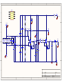
The evaluation board has separate connections for the
amplifier power supply, an output zero reference (VREF),
where: R11 = R14 and R6 + R8 = R7 + R9
On the evaluation board, the R12, R9 resistor ratio is
100:1 (499kΩ: 4.9kΩ), and RSENSE is 0.1Ω for a trans
impedance gain given by Equation 2:
and
the
current
sense
terminals.
The
correct
inter-connection between the ISENSE terminals and the
VREF terminals are needed to implement the different
types of current sense configurations.
10
[EQ.2]
The I-SENSE+ and I-SENSE- connections to the
measured circuit determine the polarity of the amplifier
Input Range and Offset Error
Analysis
output voltage. Establishing a current flow from the
I-SENSE + to I-SENSE - causes the output voltage to
The TP5532 output swings from rail-to-rail, and the
evaluation board has a bi-directional output range of VREF
±2.5V when operated from a +5V supply and VREF is set
to
VS/2.
The
evaluation
board
contains
a
jumper-selectable, internal VS/2 reference or an external
reference (VREF pin). With VREF set to +2.5, the full scale
output range is 0 ±0.25A. The very low offset voltage
(2μV +25°C max) and offset current (±100 pA +25°C max)
of the TP5532 enable the use of very high values
resistors for low current consumption while maintaining
excellent precision in battery operated circuits. The total
offset voltage contribution of the TP5532 is the sum of the
input offset voltage (VOS) and the offset voltage produced
by the input offset current (IOS) through the gain resistors
and using the evaluation board resistor values and the
data sheet maximum +25°C VOS gives the total input
I
V I-SENSE current flow reverses the output polarity.
The voltage applied to the VREF pin defines the amplifier
output zero current level, and must be between 0V and
+5V. For bi-directional current sensing, a reference
midway between the ground and the supply voltage will
maximize the output span. For example, a VREF = +2.5V
would be the best choice for +5V power supply. The
jumper selectable internal voltage divider is provided for
this internal reference. The +2.5V will establish an output
current scale setting 0A = +2.5V, but the accuracy is
determined by the voltage divider accuracy (0.1%
resistors on the evaluation board). Connecting the jumper
to the external reference position enables an external
reference source to be used. The TP5532 maintains
precision performance from rail-to-rail making precision
ground-side sensing possible.
offset voltage as shown in Equations 3, 4 and 5:
V
increase in proportion to the input current. Reversing the
(EQ.3)
Additional Feature
The TP5532 EVB can be also used for testing noise. The
V
3e
10
V
3e
10
8μV
(EQ.4)
R18, R17 resistor ratio is 100:1 (499kΩ: 4.9kΩ), The
evaluation board contains a jumper-selectable (jumper 1
4950
8μV
9.5μV
(EQ.5)
Multiplying the TP5532 input offset voltage by the
amplifier gain allows the input offset error to be expressed
as a percent of full scale output voltage.
2 REV0.0
and jumper 2) for choosing either inverting amplifier or
non-inverting
amplifier.
Resistor
R19
(4.3kΩ)
and
capacitor C22(2.2μF) work as a low pass filter which
allows the signal frequency below 16.8Hz to pass.
www.3peakic.com