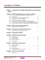
1
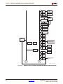
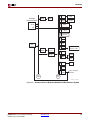
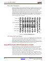
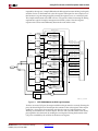
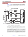
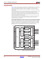
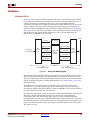
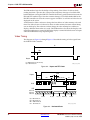
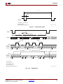
R
Chapter 5: Using IPIF to Build IP
The GPIO registers support byte enables during writes to the 32-bit registers. A set of
simple AND gates is all that is required to generate a clock enable to the registers. Four
3-input AND gates are used to drive the four bytes of the three-state control register, and
four more 3-input AND gates are used to drive the four bytes of output-pin data.
The IPIF uses a set of user-specified parameters that allow common things, such as the base
address of the IP, to be established. These parameters are specified before the system is
implemented in order to minimize the logic area and maximize the performance of the
system. Note that in the GPIO example, additional decoding is used externally to specify
two different memory locations. One location is used for reading from or writing to the
I/O pins (read register and write register share the same address), and one location is used
for 3-state control, reading and writing to the bit that controls the T of the I/O pins.
Using IPIF to Connect a Pre-Existent Peripheral to the Bus
Often, some legacy IP needs to be brought into a modern system. Many of these legacy IPs
use some form of an 8-bit microprocessor bus. Typically, this might consist of a few address
lines, an 8-bit data bus, a read and write signal, a chip enable, a clock, a reset, and perhaps
an interrupt pin. In most instances, this kind of IP can be almost directly connected to the
IPIF SRAM module. This particular IPIF module was actually designed to serve this very
purpose.
To connect a legacy IP, simply connect the address, data, chip enable, clock, reset, and
interrupt pins to their corresponding versions in the IPIF SRAM module. Some small
amount of logic might be needed to generate a properly timed read or write signal. The
IPIF SRAM module provides separate Req/Ack pairs for read and write, because many
older peripherals require different timing for reads and writes. For read or write, the logic
between the IP and the IPIF must accomplish two things:
•
Provide the proper response time to the IPIF so the peripheral’s register can be read or
written
•
Provide the proper relationship of the read or write signal on the IP relative to the
address and data
Consider the following example: The IP might expect its write signal to be valid one clock
after address and data is valid and be held for four clock cycles to properly write the data.
After write goes invalid, the address and data must be held for one additional cycle. To
accommodate this kind of pattern, a six-stage shift register (SR) can be implemented. The D
input to the SR is tied to the Bus2IP_WrReq pin, and the Q output of the SR is tied to the
IP2Bus_WrAck pin of the IPIF. This provides the proper timing for the length of time the
cycle must be held on the bus. By using the first, second, third, and fourth taps of the SR,
and feeding them into an OR gate, a write strobe can be generated for the IP. If this write
strobe must be glitch-free, taps 0, 1, 2, and 3 could be used, OR’ed, and fed into a
synchronizing register. Xilinx FPGAs are abundantly equipped with flip-flops, so the
amount of logic is not an issue.
50
www.xilinx.com
ML40x EDK Processor Reference Design
UG082 (v5.0) June 30, 2006