1
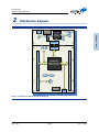
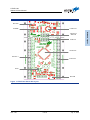
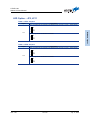
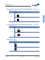
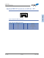
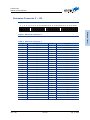
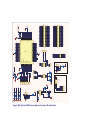
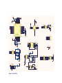
HT32F1765
Starter Kit User Manual
Revision: V1.00
Date: �������������
July 17, 2015
HT32F1765
Starter Kit User Manual
Table of Contents
1 Introduction.............................................................................................................. 5
Features.................................................................................................................................. 6
2 Hardware Layout...................................................................................................... 7
VBAT Option – JP9.................................................................................................................... 9
LED Option – JP2, JP11....................................................................................................... 10
High Speed External Crystal Oscillator (HSE) Option - JP1, JP5......................................... 11
Low Speed External Crystal Oscillator (LSE) Option – JP3, JP4......................................... 11
USB Option – JP10............................................................................................................... 11
SWD-10P Connector – JP26................................................................................................ 12
Adjustment SWD-10P Connector (for e-Link32 Lite) – JP27................................................ 13
Extension Connector 1 – J31................................................................................................ 14
Extension Connector 2 – J32................................................................................................ 15
Mini USB Type B Connector – U3........................................................................................ 16
3 Schematics............................................................................................................. 17
Rev. 1.00
2 of 20
July 17, 2015
Table of Contents
Boot Option – JP7, JP6.......................................................................................................... 9
HT32F1765
Starter Kit User Manual
List of Figures
Rev. 1.00
3 of 20
July 17, 2015
List of Figures
Figure 1. HT32F1765 Starter Kit................................................................................................................. 5
Figure 2. HT32F1765 Starter Kit Block Diagram........................................................................................ 7
Figure 3. HT32F1765 Starter Kit Layout..................................................................................................... 8
Figure 4. SWD-10P Connector................................................................................................................. 12
Figure 5. Adjustment SWD-10P Connector.............................................................................................. 13
Figure 6. Extension Connector 1.............................................................................................................. 14
Figure 7. Extension Connector 2.............................................................................................................. 15
Figure 8. Mini USB Type B Connector...................................................................................................... 16
Figure 9. MCU, Boot Pins, SWD Connector, Extension Connector, LED and the Power......................... 18
Figure 10. e-Link32 Lite............................................................................................................................ 19
HT32F1765
Starter Kit User Manual
List of Tables
Rev. 1.00
4 of 20
July 17, 2015
List of Tables
Table 1. Boot Jumpers................................................................................................................................ 9
Table 2. VBAT Jumpers................................................................................................................................. 9
Table 3. LED1 Jumpers............................................................................................................................ 10
Table 4. LED2 Jumpers............................................................................................................................ 10
Table 5. HSE Jumpers...............................................................................................................................11
Table 6. LSE Jumpers................................................................................................................................11
Table 7. USB Jumpers...............................................................................................................................11
Table 8. SWD-10P Connector................................................................................................................... 12
Table 9. Adjustment SWD-10P Connector................................................................................................ 13
Table 10. Extension Connector 1.............................................................................................................. 14
Table 11. Extension Connector 2.............................................................................................................. 15
Table 12. Mini USB Type B Connector..................................................................................................... 16
HT32F1765
Starter Kit User Manual
1
Introduction
The HT32F1765 Starter Kit is based around the 32-bit ARM CortexTM-M3 high performance
microcontroller and is designed to assist users to get up and running with this device as quickly as
possible. It provides a complete solution from evaluation, programming to production.
This development platform is composed of a Target Board and Serial-Wire Debugger (e-Link32
Lite) and as such requires no external debugging equipment. It can use the Target Board external
power supply or be powered by the Debugger.
The Starter Kit provides a standard C language program development environment for Keil μVision
and IAR EWARM. With this basis, Holtek also provides a complete function library to avoid
complicated lower level function development in order to allow development designers to focus
on the needs of their application development. Using a simple USB cable connection, users only
have to connect their PC to the integrated hardware debug interface (Serial-Wire Debugger), to
automatically download the programs and immediately commence debug operations.
Figure 1. HT32F1765 Starter Kit
Rev. 1.00
5 of 20
July 17, 2015
Introduction
The Starter Kit is based on the Cortex™-M3 high speed microcontroller, the operating frequency
is up to 72MHz. It provides 128 KB of embedded Flash memory, 64 KB of embedded SRAM
memory, multiple Timers, dual I2C interfaces, dual SPI interfaces, dual USART interfaces, 12-bit
A/D converter, 80 programmable general purpose I/O pins and a USB function which can be used
to interface to a wide range of external devices.
HT32F1765
Starter Kit User Manual
Features
▀ Comprises Target Board and Serial-Wire Debugger
▀ Can be used for the testing and development of many external devices
▀ Can use the Target Board external power supply or be powered by the Debugger
Rev. 1.00
6 of 20
July 17, 2015
Introduction
▀ Using HT32F1765 high performance microcontroller
● Up to 72 MHz operating frequency
● 128 KB Flash, 64 KB SRAM
● Integrated multiple Timers, dual I2C functions, dual SPI functions, dual USART functions,
single 12-bit A/D converter and USB function
● LQFP100 package
● 8 MHz external crystal clock
● 80 programmable general purpose I/O pins
HT32F1765
Starter Kit User Manual
2
Hardware Layout
MiniUSB
�V-to-3.3V
Reg��ator
USB LED
Err
Hardware Layout
12 MHz
HT45B0K
e-Link3�
Microcontro��er
B�s�
Adj�stment
SWD-10P
SWD-10P
LED1 LED�
3�.�68 kHz
I/O Extension-�4P
I/O Extension-�4P
HT32F1765
ARM Cortex-M3
Microcontro��er
8 MHz
RES
ET
�V-to-3.3V
Reg��ator
MiniUSB
Figure 2. HT32F1765 Starter Kit Block Diagram
Rev. 1.00
7 of 20
July 17, 2015
HT32F1765
Starter Kit User Manual
Mini USB
HT3�F1��3
HT4�B0K
SWD-10P
HT3�F1�6�
Extension 1
Extension �
Reset
Mini USB
Figure 3. HT32F1765 Starter Kit Layout
Rev. 1.00
8 of 20
July 17, 2015
Hardware Layout
Adj�stment
SWD-10P
HT32F1765
Starter Kit User Manual
Boot Option – JP7, JP6
Table 1. Boot Jumpers
Jumper
Description
Boot loader mode
C9 C8
0
Hardware Layout
1
Boot from the embedded boot loader.
SRAM mode
C9 C8
0
C8 & C9
1
Boot from the embedded SRAM.
Main flash mode – default setting
C9 C8
0
1
Boot from the embedded main flash. BOOT0 (C8) don’t care and BOOT1 (C9) = 1
VBAT Option – JP9
Table 2. VBAT Jumpers
Jumper
Description
VBAT pin is connected to 3.3V power - default setting
EXT
VBAT
VDD33
VBAT
VBAT pin is connected to 3V CR1220 battery.
EXT
VBAT
VDD33
Rev. 1.00
9 of 20
July 17, 2015
HT32F1765
Starter Kit User Manual
LED Option – JP2, JP11
Table 3. LED1 Jumpers
Jumper
Description
LED1 connected with the extension I/O header and I/O port A pin 14 (A14) – default setting
I/O
A14
LED1
Hardware Layout
A14
A14 can only connect to extension I/O header.
I/O
A14
LED1
Table 4. LED2 Jumpers
Jumper
Description
LED2 connected with the extension I/O header and I/O port A pin 15 (A15) – default setting
I/O
A15
LED2
A15
A15 can only connect to extension I/O header.
I/O
A15
LED2
Rev. 1.00
10 of 20
July 17, 2015
HT32F1765
Starter Kit User Manual
High Speed External Crystal Oscillator (HSE) Option - JP1, JP5
Table 5. HSE Jumpers
Jumper
Description
HSE mode – default setting
B11 B12
I/O
I/O
Hardware Layout
OSCOUT
OSCIN
B11 & B12
I/O mode of I/O port B pin 11 (B11) and I/O port B pin 12 (B12).
B11 B12
I/O
I/O
OSCOUT
OSCIN
Low Speed External Crystal Oscillator (LSE) Option – JP3, JP4
Table 6. LSE Jumpers
Jumper
Description
LSE mode – default setting
B4
B5
I/O
I/O
OSC32IN
B4 & B5
OSC32OUT
I/O mode of I/O port B pin 4 (B4) and I/O port B pin 5 (B5).
B4
I/O
OSC32IN
B5
I/O
OSC32OUT
USB Option – JP10
Table 7. USB Jumpers
Jumper
Description
USB detect pin connected with the extension I/O header and I/O port A pin 13 (A13) – default
setting
I/O
A13
A13
USBDP
A13 can only connect to extension I/O header.
I/O
A13
USBDP
Rev. 1.00
11 of 20
July 17, 2015
HT32F1765
Starter Kit User Manual
SWD-10P Connector – JP26
� 4 6 8 10
Hardware Layout
1 3 � � 9
Figure 4. SWD-10P Connector
Table 8. SWD-10P Connector
Rev. 1.00
Pin#
Description
Pin#
Description
1
3.3V
2
SWDIO (PE13)
3
GND
4
SWCLK (PE12)
5
GND
6
TRACESWO (PE11)
7
5V
8
NC
9
GND
10
Reset#
12 of 20
July 17, 2015
HT32F1765
Starter Kit User Manual
Adjustment SWD-10P Connector (for e-Link32 Lite) – JP27
1 3 � � 9
Hardware Layout
� 4 6 8 10
Figure 5. Adjustment SWD-10P Connector
Table 9. Adjustment SWD-10P Connector
Rev. 1.00
Pin#
Description
Pin#
Description
1
3.3V
2
SWDIO (PE13)
3
GND
4
SWCLK (PE12)
5
GND
6
TRACESWO (PE11)
7
5V
8
NC
9
GND
10
Reset#
13 of 20
July 17, 2015
HT32F1765
Starter Kit User Manual
Extension Connector 1 – J31
� 4 6 8 10 1� 14 16 18 �0 �� �4 �6 �8 30 3� 34 36 38 40 4� 44 46 48 �0 �� �4
3 � �
9 11 13 1� 1� 19 �1 �3 �� �� �9 31 33 3� 3� 39 41 43 4� 4� 49 �1 �3
Figure 6. Extension Connector 1
Table 10. Extension Connector 1
Pin#
Rev. 1.00
Description
Pin#
Description
1
A0
2
A1
3
A2
4
A3
5
A4
6
A5
7
A6
8
A7
9
A8
10
A9
11
A10
12
A11
13
A12
14
A13 (USB Option)
15
A14 (LED1 Option)
16
A15 (LED2 Option)
17
B0
18
B1
19
B2
20
B3
21
B4 (LSE Option)
22
B5 (LSE Option)
23
B6
24
B7
25
B8
26
B9
27
B10
28
B11 (HSE Option)
29
B12 (HSE Option)
30
B13
31
B14
32
B15
33
C0
34
C1
35
C2
36
C3
37
C4
38
C5
39
C6
40
C7
41
Reset#
42
VBAT (VBAT Option)
43
3.3V
44
3.3V
45
3.3V
46
3.3V
47
GND
48
GND
49
GND
50
GND
51
NC
52
NC
53
NC
54
NC
14 of 20
July 17, 2015
Hardware Layout
1
HT32F1765
Starter Kit User Manual
Extension Connector 2 – J32
� 4 6 8 10 1� 14 16 18 �0 �� �4 �6 �8 30 3� 34 36 38 40 4� 44 46 48 �0 �� �4
3 � �
9 11 13 1� 1� 19 �1 �3 �� �� �9 31 33 3� 3� 39 41 43 4� 4� 49 �1 �3
Figure 7. Extension Connector 2
Table 11. Extension Connector 2
Pin#
Rev. 1.00
Description
Pin#
Description
1
E14
2
E15
3
E12 (SWCLK)
4
E13 (SWDIO)
5
E10
6
E11 (TRACESWO)
7
E8
8
E9
9
E6
10
E7
11
E4
12
E5
13
E2
14
E3
15
E0
16
E1
17
D14
18
D15
19
D12
20
D13
21
D10
22
D11
23
D8
24
D9
25
D6
26
D7
27
D4
28
D5
29
D2
30
D3
31
D0
32
D1
33
C14
34
C15
35
C12
36
C13
37
C10
38
C11
39
C8 (Boot Option)
40
C9 (Boot Option)
41
3.3V
42
3.3V
43
3.3V
44
3.3V
45
GND
46
GND
47
GND
48
GND
49
GND
50
GND
51
5V
52
5V
53
5V
54
5V
15 of 20
July 17, 2015
Hardware Layout
1
HT32F1765
Starter Kit User Manual
Mini USB Type B Connector – U3
1
�
3
4
�
Hardware Layout
Figure 8. Mini USB Type B Connector
Table 12. Mini USB Type B Connector
Rev. 1.00
Pin#
Description
Pin#
Description
1
USB_5V
2
D-
3
D+
4
NC
5
GND
16 of 20
July 17, 2015
HT32F1765
Starter Kit User Manual
3
Schematics
This section shows the complete circuit of the HT32F1765 Starter kit:
▀ Figure 9 Includes the MCU, Boot Pins, SWD Connector, LED Display, Extension Connector and
the Power.
Rev. 1.00
17 of 20
Schematics
▀ Figure 10 Includes the e-Link32 Lite.
July 17, 2015
F_PA0
F_PA2
F_PA4
F_PA6
F_PA8
F_PA10
F_PA12
F_PA14_T
F_PB0
F_PB2
F_PB4
F_PB6
F_PB8
F_PB10
F_PB12
F_PB14
F_PC0
F_PC2
F_PC4
F_PC6
F_NRST
VDD3V3
VDD3V3
GND
GND
VIN
VIN
C37
R8
Res1
100K F_NRST
JP2
JP1
Header 3
R31
R1A
R2A
R3A
R4A
R1B
R2B
R3B
R4B
JP10
8
7
6
5
1
2
3
F_PA13_T
1
2
3
4
VDD3V3
Header 3
R37
R1A
R2A
R3A
R4A
R1B
R2B
R3B
R4B
VDD5V
1
C13
10UF
SS-12W,SS-13W,SS-14W
C42
10UF
5V_t
LED
D2
R1
R8P4R_1K
R1A
R2A
R3A
R4A
3
2
1
JP5
Header 3
VDD5V
Res1 1M
2
1
2
C3
10UF
XTAL
XTAL32
C12
Cap
7pF
Y2
VDD5V
C6
Cap
7pF
C5
Cap
10pF
C4
Cap
10pF
6
7
8
9
VDD3V3
D7
1
2
3
4
Y3
OSCOUT
OSCIN
OSC32OUT
OSC32IN
Res1 10M
D10
5V_t
LED
D4
8
7
6
5
R8P4R_330
Header 3
U2
HT7333
R2
VDD3V3
GND
GND
VDD5V
GND
U11
LM1117
VIN
1
2
3
4
1
2
3
4
VIN
GND
F_PB9
F_PB8
D12
R7
2
4
6
8
10
1
2
3
4
JP4
Header 3
3
2
1
3
2
1
3
2
1
3
2
1
JP3
Header 3
1
3
5
7
9
F_NRST
LED
JP9
Header 3
JP26
SWDIO
SWCLK
JTDO
D6
F_PA15_T
F_PA15_T
3
2
1
F_PB12
OSCOUT
OSCOUT
F_PB11
OSCIN
OSCIN
F_PB5
OSC32OUT
OSC32OUT
Cap
0.1uF
F_PB4
OSC32IN
OSC32IN
C7
SW-PB
JP11
F_PE15
SWDIO
JTDO
F_PE9
F_PE7
F_PE5
F_PE3
F_PE1
F_PD15
F_PD13
F_PD11
F_PD9
F_PD7
F_PD5
F_PD3
F_PD1
F_PC15
F_PC13
F_PC11
F_PC9
VDD3V3
VDD3V3
GND
GND
GND
VDD5V
VDD5V
2
4
6
8
10
12
14
16
18
20
22
24
26
28
30
32
34
36
38
40
42
44
46
48
50
52
54
Header 3
F_PA14_T
F_PA14_T
Header 3
C38
Cap
0.1uF
2
4
6
8
10
12
14
16
18
20
22
24
26
28
30
32
34
36
38
40
42
44
46
48
50
52
54
Header 5X2
F_PC9
F_PC8
F_DP
3
2
1
Cap
0.1uF
B1
Cap
0.1uF
1
3
5
7
9
11
13
15
17
19
21
23
25
27
29
31
33
35
37
39
41
43
45
47
49
51
53
Header 27x2
R8P4R_1.5K
C35
VBAT
VDD3V3
VDD3V3
C28
0.1UF
Header 3
C40
J32
JP7
8
7
6
5
Cap
2.2uF
1
3
5
7
9
11
13
15
17
19
21
23
25
27
29
31
33
35
37
39
41
43
45
47
49
51
53
Header 27x2
JP6
U8
VDD3V3
GND
F_PB13
F_PB14
F_PB15
F_PC0
F_PC1
F_PC2
F_PC3
F_PC4
F_PC5
F_PB6
F_PB7
F_PB8
F_PB9
F_PB10
VDD3V3
GND
F_NRST
VDD3V3
C10
F_PE14
SWCLK
F_PE10
F_PE8
F_PE6
F_PE4
F_PE2
F_PE0
F_PD14
F_PD12
F_PD10
F_PD8
F_PD6
F_PD4
F_PD2
F_PD0
F_PC14
F_PC12
F_PC10
F_PC8
VDD3V3
VDD3V3
GND
GND
GND
VDD5V
VDD5V
R1B
R2B
R3B
R4B
HT32F1765
F_PD7
F_PD6
F_PD5
F_PD4
F_PD3
F_PD2
F_PD1
F_PD0
F_PC15
F_PC14
F_PC13
F_PC12
F_PC11
GND
VDD3V3
F_PE15
F_PE14
SWDIO
SWCLK
JTDO
F_PC10
F_PC9
F_PC8
F_PC7
F_PC6
75
74
73
72
71
70
69
68
67
66
65
64
63
62
61
60
59
58
57
56
55
54
53
52
51
PD7
PD6
PD5
PD4
PD3
PD2
PD1
PD0
PC15
PC14
PC13
PC12
PC11
VSS33_4
VDD33_3
PE15
PE14
PE13
PE12
PE11
PC10
PC9
PC8
PC7
PC6
26
27
28
29
30
31
32
33
34
35
36
37
38
39
40
41
42
43
44
45
46
47
48
49
50
Cap
0.1uF
PA0
PA1
PA2
PA3
PA4
PA5
PA6
PA7
PA8
PA9
PA10
PA11
PA12
VDD33_1
VSS33_1
USBDP
USBDM
PA13
PA14
PA15
PB0
PB1
PB2
PB3
NC
VLDOOUT
VLDOIN
VSSLDO
nRST
VBAT
PB4/OSC32IN
PB5/OSC32OUT
PB6/RTCOUT
PB7
PB8
PB9
PB10
OSCIN
OSCOUT
VDD33_2
VSS33_2
PB13
PB14
PB15
PC0
PC1
PC2
PC3
PC4
PC5
C36
1
2
3
4
5
6
7
8
9
10
11
12
13
14
15
16
17
18
19
20
21
22
23
24
25
GND
VDD3V3
VDD3V3
F_PA0
F_PA1
F_PA2
F_PA3
F_PA4
F_PA5
F_PA6
F_PA7
F_PA8
F_PA9
F_PA10
F_PA11
F_PA12
VDD3V3
GND
F_DP
F_DM
F_PA13_T
F_PA14_T
F_PA15_T
F_PB0
F_PB1
F_PB2
F_PB3
VSSA
VREFVREF+
VDDA
PE10
PE9
PE8
PE7
PE6
PE5
PE4
PE3
PE2
PE1
VSS33_4
VDD33_4
PE0
PD15
PD14
PD13
PD12
PD11
PD10
PD9
PD8
100
99
98
97
96
95
94
93
92
91
90
89
88
87
86
85
84
83
82
81
80
79
78
77
76
Inductor
10mH
F_PA1
F_PA3
F_PA5
F_PA7
F_PA9
F_PA11
F_PA13_T
F_PA15_T
F_PB1
F_PB3
F_PB5
F_PB7
F_PB9
F_PB11
F_PB13
F_PB15
F_PC1
F_PC3
F_PC5
F_PC7
VBAT
VDD3V3
VDD3V3
GND
GND
VIN
VIN
2
4
6
8
10
12
14
16
18
20
22
24
26
28
30
32
34
36
38
40
42
44
46
48
50
52
54
2
4
6
8
10
12
14
16
18
20
22
24
26
28
30
32
34
36
38
40
42
44
46
48
50
52
54
1
2
3
C9
Cap
0.1uF
L2
1
3
5
7
9
11
13
15
17
19
21
23
25
27
29
31
33
35
37
39
41
43
45
47
49
51
53
VDD3V3
C11
Cap
2.2uF
F_PE10
F_PE9
F_PE8
F_PE7
F_PE6
F_PE5
F_PE4
F_PE3
F_PE2
F_PE1
GND
VDD3V3
F_PE0
F_PD15
F_PD14
F_PD13
F_PD12
F_PD11
F_PD10
F_PD9
F_PD8
Cap
0.1uF
J31
GND
L1
Inductor
10mH
1
3
5
7
9
11
13
15
17
19
21
23
25
27
29
31
33
35
37
39
41
43
45
47
49
51
53
1
2
3
VDD3V3
U3
GND VDD
GNDUSBDGNDUSBD+
GND VSS
SHELL
SS-12W,SS-13W,SS-14W
1
2
3
4
5
USB_CONNECTOR
SS-12W,SS-13W,SS-14W
C8
10UF
C18
0.1uF
R4
F_DM
R13 33
F_DP
F_PB7
J4
1
2
3
4
5
6
HEADER 6
33
C32
47p
C1
47p
R11
Res1
1M
Title
Size
A2
Figure 9. MCU, Boot Pins, SWD Connector, Extension Connector, LED and the Power
Number
Revision
C21
Cap
0.1uF
VDD3V3
C27
Cap
2.2uF
C22
Cap
0.1uF
VDD3V3
VDD3V3
PA14/SWCLK
PA13/SWDIO
1
2
3
4
R36
R1A
R2A
R3A
R4A
R1B
R2B
R3B
R4B
LED
8
7
6
5
PA9/UR_TX
1
2
PA7/SPI_SEL 3
PA5/SPI_MISO4
5
PA3
PA2
6
7
8
VDD3V3
Res1
100K
U10
SDI
NC
SCK
SCS
CLKI
INT
VSS
NC
SDO
NC
V33O
UDP
UDN
VDD
VDD
VSS
PA8/UR_RX
16
15
14
13
12
11
10
9
3
C
E
U7
MMBT3904_SOT23
JP8
1
2
3
4
5
PB0/OSCI
PB1/OSCO
Y1
1
2
3
CRYSTAL
VDD5V
D5
6
7
8
9
SS-12W,SS-13W,SS-14W
U5
GND VDD
GNDUSBDGNDUSBD+
GND VSS
SHELL
VDD3V3
R12
1
2
3
4
5
R5
33
VDD3V3
GND
GND
VDD5V
GND
33
C2
47p
C31
47p
JP27
1
3
5
7
9
SWDIO
SWCLK
JTDO
PB2
F_NRST
2
4
6
8
10
Header 5X2
R33
R1A
R2A
R3A
R4A
R1B
R2B
R3B
R4B
8
7
6
5
R8P4R_10K
R1A
R2A
R3A
R4A
R1B
R2B
R3B
R4B
R8P4R_1.5K
8
7
6
5
E
R34
3
1
2
3
4
2
PA6/SPI_SCK
C
D9
SS-12W,SS-13W,SS-14W
1
2
3
4
R10
Res1
1M
B
C17
0.1uF
1
VDD3V3
1
2
3
4
R8P4R_10K
VDD3V3
USB_CONNECTOR
C34
10UF
GND
VDD3V3
LED
C14
10UF
8
7
6
5
C39
Cap
0.1uF
HT45B0K
LED
D8
VDD5V
R1B
R2B
R3B
R4B
Header 5
LED
D3
U4
HT7333
R1A
R2A
R3A
R4A
B
SWDIO
SWCLK
GND
5
4
3
F_NRST
R32
2
7
6
B1
B2
GND
1
2
3
4
VDD3V3
GND
PA14/SWCLK
PA13/SWDIO
NRST
D11
R8P4R_330
A1
A2
DIR1
C26
Cap
0.1uF
D1
VDD3V3
PB7
PB6
PB5
8
9
10
VDD3V3
PB12
GND
PA11/I2C_SCL
1
VDD3V3
U9
SN74AVC2T245
VCCA
VCCB
R6
Res1
470 PB14
PB13
PB2
1
2
PB1/OSCO
PB0/OSCI
PB15
PB14
PB13
PB12
PB12
GND
36
35
34
33
32
31
30
29
28
27
26
25
Cap
0.1uF
HT1253_LQFP48
R9
C16
0.1UF
PB15
VSSA_1
VDDA
VSS33_1
VDD33_1
PB7
PB6
PB5
PB4
PB3
PB2
N.C.
VDD18
PB1/OSCO
PB0/OSCI
PB15
PB14
PB13
PB12
VSS33_3
VSS33_2
VDD33_2
PA15
PA14
PA13
VLDOOUT
N.C.
VLDOIN
VSSLDO
nRST
VBAT
PB8/OSC32I
PB9/OSC32O
PB10
PB11
PA11
PA12
VSSA_2
PA0
PA1
PA2
PA3
PA4
PA5
PA6
PA7
PA8
PA9
PA10
U1
13
14
15
16
17
NRST
VDD3V3
18
19
20
21
22
PA11/I2C_SCL 23
JTDO
24
1
2
3
4
PA2
PA3
5
6
PA5/SPI_MISO7
PA6/SPI_SCK 8
PA7/SPI_SEL 9
PA8/UR_RX 10
PA9/UR_TX 11
12
C41
DIR2
OE
48
47
46
45
44
43
42
41
40
39
38
37
C23
Cap
0.1uF
PB2
PB7
PB6
PB5
VDD3V3
U6
MMBT3906_SOT23
Title
VDD3V3
Size
Number
Revision
A4
Date:
Figure 10. e-Link32 Lite
2015/6/18
Sheet of
HT32F1765
Starter Kit User Manual

Copyright© 2015 by HOLTEK SEMICONDUCTOR INC.
The information appearing in this Data Sheet is believed to be accurate at the time
of publication. However, Holtek assumes no responsibility arising from the use of
the specifications described. The applications mentioned herein are used solely
for the purpose of illustration and Holtek makes no warranty or representation that
such applications will be suitable without further modification, nor recommends
the use of its products for application that may present a risk to human life due to
malfunction or otherwise. Holtek's products are not authorized for use as critical
components in life support devices or systems. Holtek reserves the right to alter
its products without prior notification. For the most up-to-date information, please
visit our web site at http://www.holtek.com.tw.
Rev. 1.00
20 of 20
July 17, 2015